
Colloidal Nanoparticle Inks for Printing Functional Devices
80
Colloidal Nanoparticle Inks for Printing Functional Devices: Emerging Trends and Future Prospects Journal: Journal of Materials Chemistry A Manuscript ID TA-REV-07-2019-007552.R1 Article Type: Review Article Date Submitted by the Author: 16-Sep-2019 Complete List of Authors: Zeng, Minxiang; University of Notre Dame, Department of Aerospace and Mechanical Engineering Notre Dame Zhang, Yanliang; University of Notre dame, Department of Aerospace and Mechanical Engineering Journal of Materials Chemistry A
-
Upload
khangminh22 -
Category
Documents
-
view
3 -
download
0
Transcript of Colloidal Nanoparticle Inks for Printing Functional Devices

Colloidal Nanoparticle Inks for Printing Functional Devices: Emerging Trends and Future Prospects
Journal: Journal of Materials Chemistry A
Manuscript ID TA-REV-07-2019-007552.R1
Article Type: Review Article
Date Submitted by the Author: 16-Sep-2019
Complete List of Authors: Zeng, Minxiang; University of Notre Dame, Department of Aerospace and Mechanical Engineering Notre DameZhang, Yanliang; University of Notre dame, Department of Aerospace and Mechanical Engineering
Journal of Materials Chemistry A

1
Colloidal Nanoparticle Inks for Printing Functional Devices: Emerging
Trends and Future Prospects
Minxiang Zeng, Yanliang Zhang*
Department of Aerospace and Mechanical Engineering, University of Notre Dame, Notre Dame, IN, USA
*Corresponding Author: [email protected]
ABSTRACT
Colloidal nanoparticles have been widely studied and proven to have unique and superior
properties compared to their bulk form, which are attractive building blocks for diverse
technologies, including energy conversion and storage, sensing, electronics, etc. However,
transforming colloidal nanoparticles into functional devices while translating their unique
properties from nanoscale to macroscale remains a major challenge. The development of
advanced manufacturing methodologies that can convert functional nanomaterials into high-
performance devices in a scalable, controllable and affordable manner presents great research
opportunities and challenges for the next several decades. One promising approach to fabricate
functional devices from nanoscale building blocks is additive manufacturing, such as 2D and 3D
printing, owing to their capability of fast prototyping and versatile fabrication. Here, we review
recent progresses and methodologies on additive printing of functional devices using colloidal
nanoparticles inks with an emphasis on 2D nanomaterial-based inks. This review provides a
comprehensive overview on four important and interconnected topics, including nanoparticle
synthesis, ink formulation, printing methods, and device applications. New research opportunities
as well as future directions are also discussed.
KEYWORDS: colloidal nanoparticles, ink printing, functional devices
Page 1 of 79 Journal of Materials Chemistry A

2
Table of Content
1. Introduction .........................................................................................................................32. Synthesis of 2D nanomaterials............................................................................................6
2.1. Bottom-up synthesis .....................................................................................................72.2. Top-down synthesis ....................................................................................................10
3. Ink formulation..................................................................................................................163.1. The colloidal stability of 2D nanomaterials................................................................173.2. Ink rheology of 2D nanomaterials ..............................................................................253.3. Ink drying and particle assembly ................................................................................27
4. Printing strategies..............................................................................................................304.1. 2D printing ..................................................................................................................314.2. 3D printing ..................................................................................................................354.3. 4D printing ..................................................................................................................39
5. Device applications of printed 2D nanomaterials ...........................................................435.1. Energy conversion and storage ...................................................................................435.2. Sensing........................................................................................................................51
6. Conclusion and Future Perspectives................................................................................60
Page 2 of 79Journal of Materials Chemistry A

3
1. Introduction
Colloidal nanoparticles are attractive building blocks for a wide range of emerging
technologies, including electronics, optoelectronics, sensors, energy devices, etc. In the past
several decades, various device fabrication technologies, such as photolithography, electroless
plating, and physical/chemical vapor deposition, have been extensively investigated.1, 2 However,
these technologies rely on expensive equipment and/or multi-stage processes, which are not only
difficult for fast prototyping and low-cost manufacturing, but also not compatible/sophisticated
enough for building functional devices with colloidal nanoparticles. An alternative method to
fabricate flexible/functional devices is additive manufacturing, such as three-dimensional (3D)
printing.3, 4 In the past several decades, significant development of printing technologies has been
witnessed for converting printable nanoparticle inks into complex device architectures.5-7 A wide
range of functional nanomaterials from zero-dimension (0D) quantum dots, to one-dimensional
(1D) nanowires/nanofibers, and two-dimensional (2D) nanosheets, have been adopted as printable
colloidal inks (Figure 1). All these progresses have created almost infinite possibilities for rapid
prototyping and scalable and low-cost manufacturing of functional devices.8
Figure 1. Additive manufacturing enables rapid transformation from nanoscale building blocks
into macroscale functional devices. Adapted and reprinted by permission from Springer Nature.9,
10 Copyright 2017&2018 Nature Publishing Group. Reproduced with permission
from reference.11 Copyright 2013 American Chemical Society.
Page 3 of 79 Journal of Materials Chemistry A

4
Among various types of nanomaterials, 2D nanomaterials (2DM) are ultrathin
nanostructures with unique optical, electrical, chemical, thermal and mechanical properties.12, 13
Since the rise of graphene family, a great variety of 2D nanomaterials have been synthesized and
developed by bottom-up strategy from molecular precursors or top‐down approach from their
layered crystals.14 As shown in Figure 2, common 2D nanomaterials include graphene/graphene
oxide/reduced graphene oxide (Gr/GO/rGO), transition metal dichalcogenides (TMDs), transition
metal carbides/carbonitrides/nitrides (MXenes), black phosphorus (BP), hexagonal boron nitride
(h‐BN), graphitic carbon nitride (g‐C3N4), layered double hydroxides (LDHs), transitional metals/
metal oxides (TMOs/MOs), and other novel 2D nanostructures.12 Graphene is a monolayer
graphite with every carbon atom bonded to adjacent ones by σ bond, forming hexagonal 2D
network with a thickness around 3.4 Å. TMDs also have a hexagonal surface structure similar to
graphene, with the in‐plane anion atoms in each layer split into two identical layers. MXenes are
of general formula Mn+1XnTx (n = 1–3), where M is transition metal (e.g., Ti or V), X is C and/or
N, and T is surface anion (O, OH, F). For natural occurring 2DMs, clay minerals are 2D sandwich
structures with octahedral metal hydroxide layers and tetrahedral silicate layers.15 LDHs, also
known as anionic clays or hydrotalcite‐like compounds, are often described by the general
formula, [M2+1−xM3+
x(OH)2]x+An−x/n.yH2O, where M is metal ion and A represents an interlayer
anion.16, 17
Page 4 of 79Journal of Materials Chemistry A

5
Figure 2. 2D nanomaterials and their structures. Reproduced with permission from reference.18
Copyright 2018 Wiley-VCH.
The extreme chemical diversity of 2D nanomaterials provides many opportunities, but
also poses challenges for comprehensive assessments of specialized roles of 2DMs in device
fabrication processes, such as printing-based manufacturing. In addition, high-performance 2D
nanomaterials are not necessarily translated into high-quality inks for printing processes. The
collective behaviour of 2D nanoparticles in colloidal inks can be influenced by many factors, such
as particle size and surface chemistry, tendency of aggregation, ionic strength of the dispersion.
Although several articles have made great effort on reviewing printing technologies of
nanomaterials,3, 4, 7, 19-22 a comprehensive review that covers nanoscale building blocks (e.g.,
synthesis and surface engineering), mesoscopic colloidal interaction (e.g., aggregation and
sedimentation), and macroscopic printing processes (e.g., 2D, 3D, and 4D printing) and device
applications is missing. This review therefore proposes a framework for seeking a systematic
understanding on fundamental correlations of materials chemistry and physics of 2DMs, ink
Page 5 of 79 Journal of Materials Chemistry A

6
properties, printing processes, and corresponding device applications. With this in mind, the
framework thus considers four key interactive aspects: 2D nanomaterial synthesis, ink
formulation, printing processes, and device applications. Our vision is to undertake a meticulous
examination of current research trends over the last decade with a focus on 2DMs compatible
with printing processes. The review closes with a conclusion and outlook, suggesting future
directions to inform researchers potentially disruptive printing technologies and applications of
2DMs.
2. Synthesis of 2D nanomaterials
Since the discovery of graphene, significant efforts have been invested on the synthesis
of 2D materials, including liquid phase exfoliation, hydrothermal synthesis, etc. In this section,
we mainly focus on solution-processable 2D nanomaterials such that some synthetic methods
such as chemical vapor deposition will not be discussed. The synthetic strategies of 2D
nanomaterials typically can be categorized into two kinds: bottom-up synthesis and top-down
synthesis. Despite some exceptions, Table 1 aims to summarize the common preparation methods
for 2D nanomaterials. Despite that not all of these synthetic methods have been explored for ink
preparation, significant research opportunities still exist for synthesizing novel printable 2D
nanostructures and establishing next-generation material library for printing technology as well
as for developing new printing methodologies for a broad range of device applications.
Table 1: Overview of various 2D nanomaterials with their common preparation methods.
Bottom-up Top-down
Hydrothermal/Solvothermal
Ligand/Template attachment
Self-assembly
Micro-mechanical cleavage
Liquid exfoliation
Selective etching
Gr/GO/rGO +23, 24 +25, 26 +27, 28
TMDs +29 +30 +31 +32 +33, 34
h‐BN +35, 36 +37 +38
Black phosphorus
+39 +40
Page 6 of 79Journal of Materials Chemistry A

7
Metal oxides
+41 +42, 43 +44 +45
MXene +46 +47
Clays +48 +49
Comments Facile and applicable to large-scale production.
Provide good control on particle size and morphology.
Versatile but low structural robustness due to non-covalent bonding.
Good quality while often low yield.
High scalability and relatively low cost.
Strongly corrosive agents are often required.
2.1. Bottom-up synthesis
2.1.1 Hydrothermal/Solvothermal synthesis
As a representative wet-chemical synthesis approach, the hydrothermal/solvothermal
synthesis involves water or other solvents in a sealed vessel, where reaction temperature can be
higher than the boiling point of the solvent in order to generate high pressure to assist the reaction
kinetics and increase the quality of crystal phase of as-prepared 2D nanomaterials.12 Remarkably,
the solvent and additives, such as ligands or surfactants, are crucial factors in determining the
synthesis, morphology, and properties of 2D nanosheets. For example, ultrathin cobalt nanosheets
with tunable oxide state can be prepared by using hydrothermal condition of butylamine and
dimethylformamide (Figure 3a).50 Single-layer noble metal nanosheets with lateral sizes of few
hundred nanometers can be prepared using polyvinylpyrrolidone (PVP) as surfactants. Besides
metal nanosheets, metal oxides and TMDs nanosheets have also been produced by
hydrothermal/solvothermal techniques.
Page 7 of 79 Journal of Materials Chemistry A

8
Figure 3. Examples of bottom-up synthesis of 2D nanomaterials. (a) Hydrothermal synthesis of
cobalt nanosheets. Reprinted by permission from Springer Nature.50 Copyright 2016 Nature
Publishing Group. (b) Colloidal synthesis of WS2 from small molecules. The formation of 1T-
WS2 and 2H-WS2 can be actively controlled by adjusting reaction conditions. Reprinted by
permission from reference.51 Copyright 2014 The Royal Society of Chemistry. (c) The bottom‐up
synthesis of Al2O3 nanosheets based on the 2D templates of GO reacting with basic aluminum
sulfate (BAS). Reproduced with permission from reference.30 Copyright 2016 Wiley-VCH. (d)
Evaporation-induced bottom-up self-assembly approach for fabricating 2D porous carbon
nanosheets. Reprinted by permission from reference.52 Copyright 2019 The Royal Society of
Chemistry.
Page 8 of 79Journal of Materials Chemistry A

9
Although the hydrothermal/solvothermal synthesis is a facile and possibly scalable
technique for producing 2DMs, it is difficult to fully understand the mechanisms in every single
reaction as all the reaction kinetics occurs in a sealed system, which make it challenging to apply
the same experimental condition to other 2DMs systems. Noteworthy, the hydrothermal synthesis
is relatively sensitive to the experimental settings, which increase the challenge of precisely
controlling the resulting 2D nanomaterials in different batches or different laboratories.
2.1.2 Ligand/template attachment method
Compared with traditional hydrothermal mechanism, the ligand attachment method
demonstrates an unusual growth progression and realizes nanostructures with well-defined
shapes.53 During this process, neighboring nanocrystals or precursors are accumulated, attached,
and fused with each other, forming single-crystalline 2D sheets to reduce high interfacial energy
facets.12 For example, taking advantage of the strong bonding of oleic acid on [100] facet, small
PbS nanocrystals can grow into single-crystalline 2D PbS sheets. Studies also showed that other
reagents, such as chlorine-containing reactants, can assist activating the oriented attachment
progression. In general, the growth mechanism is typically based on oriented attachment of small
crystals, after which epitaxial recrystallization into large 2D nanostructures occurs. Similar to
hydrothermal mechanism, surfactants are critical for determining the size, shape, and
nanostructures of 2DMs in ligand attachment method. As shown in Figure 3b, Mahler et al.
demonstrated that the formation of either 2H-WS2 or 1T-WS2 highly depends on the ligand
choice.51 Introducing small amount of hexamethyldisilazane (HMDS) into reaction system can
lead to the formation of semiconducting 2H-WS2 rather than the metallic 1T-WS2.
Similar to the ligand attachment method, other templated strategies have been
investigated for growing anisotropic nanostructures. As shown in Figure 3c, 2D GO nanosheets
were used as 2D template to direct the growth of inorganic Al2O3 sheets.30 During the synthesis,
a thin layer of hydroxide of aluminum was first deposited on the GO sheets which was then
removed using calcination treatment at 800 oC, leading to the transformation of aluminum
Page 9 of 79 Journal of Materials Chemistry A

10
hydroxide to the Al2O3 nanosheets. As another 2D-templated example, the hexagonal close-
packed (hcp) gold nanosheets can be prepared by using the GO as a starting template.54 In addition,
CuO nanoplates were also reported for templated synthesis of α-Fe2O3 nanosheets, in which the
CuO template was etched away during the nanosheet growth.55 Numerous 2D semiconductor
nanosheets, including CuInS2, CuInxGa1–xS2, and Cu2ZnSnS4, have also been fabricated by 2D-
templated synthesis processes.56
2.1.3 Self-assembly of building blocks
Driven by the improvement of nanocrystal production, self-assembly of small building
blocks has been developed to breed architectures with nanocrystal building blocks in an
orientationally/positionally ordered manner, where pre-synthesized building blocks instinctively
assemble with each other by physical/chemical interactions including electrostatic interactions,
van der Waals interactions, hydrogen bonds, etc.57 Both nanoparticles and nanowires were shown
to self-assemble into 2D materials, such as polycrystalline 2D CdTe nanosheet or assembled Au
nanosheets.31, 58 For example, the self-assembly of PbS nanowires has been demonstrated to
produce anisotropic PbS nanosheet.59 To better control the assembly process, interface-based self-
assembly has been proposed to fabricated functional 2D nanomaterials.52 As shown in Figure 3d,
spherical polystyrene-functionalized SiO2 nanoparticles can self-assemble at the interface of the
saturated NaCl solution and air. The 2D intermediate was then dispersed in sulfuric acid to
preserve its nanosheet morphology followed by Co treatment to dope Co element in 2D sheets.
After a simple carbonization and etching process, functional Co-modified carbon nanosheets were
obtained.52
In addition to nanocrystals, organic molecules can also be used as building blocks for
self-assembly into 2D materials by electrostatic interactions, van der Waals interactions, and
hydrogen bonds. Well-organized photonic nanosheets were demonstrated by self-assembly of
nonionic surfactant hexadecylglyceryl maleate.60 It is reasonable to expect that more novel 2D
materials would be developed via self-assembly of building blocks strategy.
Page 10 of 79Journal of Materials Chemistry A

11
2.2. Top-down synthesis
2.2.1 Micromechanical cleavage
The ability to synthesize 2D materials with desired chemical composition, dimensions,
crystalline phase, and surface properties is of particular significance. The micromechanical
cleavage technique was used to prepare 2D nanosheets by exfoliating layered crystals. For
example, using mechanical forces with Scotch tape, single/few layers of nanosheets can be
achieved as the interlayered van der Waals forces have been overcome in bulk crystals. In 2004,
Geim and co-workers first reported the micromechanical cleavage of graphite, where the bulk
graphite can be attached to Scotch tapes followed by peeling into thin platelets with another
adhesive surface.61-64 By repeating such process several times, the desired thin flakes can be
obtained. After attaching freshly cleaved thin films to a flat substrate and removing scope tapes,
single- or few-layers of graphene can be acquired.
This micromechanical cleavage technique can be extended to exfoliate other layered
materials, including MoS2, NbSe2, and h-BN.63 Recently, the micromechanical cleavage
technique has been employed to synthesize several ultrathin 2D nanomaterials ranging from
TMDs,65 to topological insulator,66 and antimonene.67 As a general method capable of fabricating
all categories of nanosheets of which bulk crystals are layered structures, additional novel
ultrathin 2D crystals are expected to be synthesized by this method. This methodology can be
considered as a nondestructive process as no chemical reactions were required during the
manufacturing process. Consequently, the exfoliated nanosheets retained the pristine crystal
quality of their layered counterparts. The dimensions of the formed 2D structures can reach
micrometer levels, which enable the mechanically cleaved nanosheet to become an ideal
candidate to investigate the intrinsic mechanical, optical, and electronic properties of 2D
nanomaterials.
Despite several advantages of the micromechanical cleavage method, disadvantages still
remain: 1) the fabrication yield of this method is relatively low, and impurities such as thick flakes
Page 11 of 79 Journal of Materials Chemistry A

12
always coexist with the single- or few-layer flakes; 2) The manufacturing speed is not competitive
to other methods such as solution-based approaches. The low yield together with the slow
manufacturing rate make it problematic to meet the requirements for many printing applications,
especially for large-scale additive manufacturing; 3) the dimensions of the prepared 2D materials
are hard to be regulated as the exfoliation route lacks the exactness, controllability, or repeatability;
4) Additional substrates are prerequisites to hold the formed 2D crystals during exfoliation,
making it challenging for fabricating freestanding 2DM-based devices. Recent efforts have been
made to improve micromechanical cleavage method, showing that using oxygen plasma treatment
with additional heating during the exfoliation substantially improved the uniformity of interface
contact and thus increased the production yield of 2D nanosheets.68
2.2.2 Mechanical liquid exfoliation
Sonication has been commonly used as sources of mechanical forces for exfoliating
layered bulk materials, which are generally dispersed in a particular solvent. As the liquid
cavitation is induced by sonication, the waves of mechanical vibrations through the layered
crystals produce an intensive tensile stress, resulting in the exfoliation of starting materials into
thin sheets.69 The 2D nanosheets can be separated from the suspension using centrifugation. To
maximize the efficiency of liquid phase exfoliation, matching the interfacial energy between
solvent and 2D materials can be an important factor. As it is relatively simple and effective
without any complicated equipment, this sonication technique offers a low-cost approach for
high-yield fabrication of 2D nanosheets. For example, a fairly high concentration of graphene
nanosheets suspension was achieved by sonicating bulk graphite in isopropanol and chloroform.70,
71 In addition to graphene, other 2D nanomaterials, including NbSe2, Bi2Te3, and h-BN have also
been prepared by this technique.72 The solvent systems play significant roles in the production of
exfoliated nanosheets. It is noteworthy that although pure H2O was constantly thought to be
unsatisfactory for efficiently exfoliating layered bulk materials, a recent study showed that direct
exfoliation and dispersion of 2D nanomaterials in pure H2O can be achieved at elevated
Page 12 of 79Journal of Materials Chemistry A

13
temperatures.73 The exfoliated nanosheets can be stabilized due to the presence of colloidal
surface charges brought by edge functionalization or high polarity, leading to enhanced colloidal
stability of 2D nanosheets. Such approach of exfoliating bulk materials in pure water makes this
process promising for practical applications due to environmentally friendly and low-cost feature.
It is challenging to find an appropriate solvent for each layered bulk material, as the
surface energy differs in different bulk crystals. Instead, the addition of polymers or surfactants
provided another promising pathway for exfoliating 2D layered materials. The surface energy of
the aqueous dispersion can be simply adjusted by introducing suitable surfactants, thus reducing
the interfacial energy between layered bulk crystals and solvent and realizing effective exfoliation
of layered constituents. For instance, pyrene derivatives are commonly used as dispersants for
manufacturing graphene dispersions owing to their ability to form π-π stacking interaction with
graphene sheets.74, 75 Through introducing repulsive electrostatic forces on graphene surface,
pyrene derivatives can prevent sheet aggregation and consequently stabilize graphene in water.76-
78 In addition to pyrene derivatives, other species have been employed for dispersing 2D
nanosheets in inks: polystyrene (PS), polyvinyl chloride (PVC), ethyl cellulose (EC),
polyvinylpyrrolidone, poly(isoprene-b-acrylic acid) (PI-b-PAA), poly[styrene-b-(2-
vinylpyridine)] (PS-b-P2VP), P-123-polyoxyethylenes orbitanmonooleate, polyoxyethylene
sorbitantrioleate, polyoxyethylene dodecyl ether, polyoxyethylene octadecylether,
polyoxyethyleneoctyl phenyl ether, bovine serum albumin (BSA), Pluronic P-123, n-dodecyl β-
d-maltoside (DBDM), and Arabic gum from acacia tree.79-82
Although the sonication-assisted exfoliation method can be applicable for a wide range
of 2D materials with higher fabrication rate than that of micromechanical cleavage processes, the
fabrication rate remains relatively low to meet the requirement for industrial scale. In order to
scale up the process, shear force-assisted method was proposed. Using a high-shear rotor-stator
mixer, high shear rates in suspension can trigger the exfoliation process and produce exfoliated
nanosheets in a much more efficient manner.83 The shear-force device contains a mixing head
Page 13 of 79 Journal of Materials Chemistry A

14
consisting of a rotor with a stator. Such technique was also used for exfoliating BP crystal into
few-layer platelets. Additionally, the synthesis of exfoliated WS2, MoS2, and h-BN nanosheets
were reported by using a kitchen blender.84 Such results suggest that it is possible to use industrial
stirring tank reactors for large-scale 2D materials production.
2.2.3 Intercalation-assisted liquid exfoliation
As a typical top-down approach, the ion intercalation strategy has been widely adopted
to fabricate ultrathin 2D nanosheets. Small molecules and ionic species, including Li+, Na+, K+,
can intercalate into the spaces between neighboring layers in layered bulk crystals, leading to the
formation of intercalated compounds (Figure 4).33, 34 Consequently, the ion intercalation can
considerably enlarge the interlayer distance of unexfoliated bulk crystals, facilitating the
exfoliation process with shorter time. High yield of mono- to few-layer nanosheets can be
achieved using a separation step to eliminate unexfoliated flakes by methods such as high-speed
centrifugation. For example, the layered materials were treated with n-butyl lithium to yield a Li-
intercalated structure in refluxed hexane solution for several days, and subsequently the nanosheet
dispersion can be readily formed under sonication in water.
In spite of the accelerated exfoliation facilitated by ion intercalation, the intercalation
process itself requires extended reaction time (for example, several days) and elevated
temperature (for instance, 100 °C) for some compounds. The lateral dimensions, quantity of
deficiencies, sheet concentration, and number of layers can be approximately adjusted by
changing the tentative settings, including starting size of layered crystals, exfoliation time,
exfoliation agents, and reaction temperature. During ion-intercalation, phase alteration sometimes
occurs from semiconducting hexagonal (2H) and metallic octahedral (1T) phase for MoS2 and
WS2, presenting a potent method for the phase engineering of TMDs.85 Despite that some ions
are able to intercalate into layered metal telluride or selenide, the use of ion intercalation strategy
for exfoliating metal telluride or selenide remains challenging, as the intercalated metal telluride
Page 14 of 79Journal of Materials Chemistry A

15
or selenide are commonly unstable, leading to the decomposition of metal telluride/selenide
during sonication.12
Figure 4. Examples of top-down synthesis of 2D nanomaterials. (a) The intercalation and (b) the
exfoliation of MoS2 using hydrazine and naphthalenide. (c) Unexfoliated MoS2 crystal. (d)
Intercalated MoS2 (e) Exfoliated MoS2 in dispersion. Reprinted by permission from Springer
Nature.34 Copyright 2014 Nature Publishing Group.
The ion intercalation route, such as the use of butyl lithium, is difficult to regulate
precisely, making it challenging to circumvent inadequate or over ion-intercalation. Recently,
safer salt choices including NaCl and CuCl2 were proposed as intercalates for the exfoliation of
graphite powder into graphene. Upon heating at 100 °C to vaporize the water, the Cu2+ or Na+ can
be intercalated into interlayer spacing of graphite.86 After sonicating in DMF or NMP for a short
time, up to 65% (1–5 layers) yield of graphene sheets can be produced with large lateral sizes up
to tens of micrometers.
2.2.4 Oxidation-assisted Liquid Exfoliation
In oxidation-assisted exfoliation of graphite, commonly known as the Hummers’ method,
strong oxidizing agents, such as potassium permanganate or sodium persulfate, were applied to
Page 15 of 79 Journal of Materials Chemistry A

16
oxidize graphite, and the oxidation of graphite produces hydrophilic functional groups on each
graphene layer, resulting in enlarged d-spacing of bulk graphite.87, 88 With increased treatment
time and temperature, the expanded graphite oxides bulk materials were exfoliated into 2D
graphene oxide monolayers, or possibly transformed into small-sized 2D graphene quantum dots.
This technique enables large-scale synthesis of single-layer GO nanosheets in aqueous solution.
It is noteworthy that the oxygen-containing functional groups of GO can be partially eliminated
using reduction strategy to form reduced GO nanosheets. Up to now, electrochemical reduction,
thermal annealing, photochemical reduction, and chemical reduction were reported to remove
GO’s oxygen-containing groups.89 Since the residual groups may still exist, the conductivity of
reduced GO commonly cannot compete with graphene nanosheets produced from CVD method
or mechanical exfoliation.
2.2.5 Selective etching
The selective etching method can prepare 2D nanosheets of MXenes, a type of metal
carbides or carbonitrides.90, 91 MAX phases have a common formula of Mn+1AXn (n = 1, 2, or 3),
where M, A, and X represent early transition metal, element of group IIIA or IVA, and C and/or
N, respectively.92-94 A clear difference between MAX phase materials and conventional van der
Waals layered crystals lies in the metallic bonds between Mn+1Xn layers which shows much more
robust interaction than weak forces of TMDs, graphite, and BP. Consequently, an elective etching
technique based on acidic HF solution is often required to remove the “A” layers without
destroying the bonds in Mn+1Xn layers. The resulting etched materials with loosely packed layers
can be readily exfoliated into 2D nanosheets under sonication. Up to now, this technique has been
magnificently useful for synthesizing many different types of MXenes including Al3C3, Ta4C3,
Mo2TiC2, Nb2C, Ti4N3, Mo2Ti2C3, Ti3CN, Mo2CTx, Cr2TiC2, Ti2C, V2C, (Ti0.5,Nb0.5)2C, and
(V0.5,Cr0.5)3C2. However, several limitations still exist in this technique as it is difficult to apply
this process to prepare other ultrathin 2D nanosheets, such as TMDs.
3. Ink formulation
Page 16 of 79Journal of Materials Chemistry A

17
While 2D materials show intriguing properties at the nanoscale, these particles cannot be
directly used until being processed and formulated into printable inks for device fabrication. One
important goal of ink formulation is to convert or integrate nanoscale building blocks into a stable
colloidal dispersion. The use of 2DM-based inks for printing has received increasing research
interests in recent years, likely due to: (i) significant advances in solution-processable 2DMs and
2DM derivatives on which the surface chemistry and nanostructure can be on-demand controlled,
and (ii) fast development of printing technologies that provides a variety of processing options.
Herein, major principles of colloidal ink systems and recent developments in 2DM-based inks are
discussed.
3.1. The colloidal stability of 2D nanomaterials
For most nanoparticle-based inks, the colloidal stability of the ink particles is one of the
most essential elements in preparation of high-quality inks. In a liquid medium, the colloidal
behavior of 2D nanomaterials can be estimated through the Derjaguin-Landau-Verwey-Overbeek
(DLVO) theory, which predicts the aggregation trend of nanoparticles quantitatively. As shown
in Figure 5a, DLVO theory combines the potential energy of the van der Waals attraction (PA,
red) and the electrostatic repulsion (PR, blue) because of the electric double layers. Figure 5a also
presents a typical total energy profile (Ptotal, green) along with the separation distance of particles:
the primary minimum and secondary minimum represent the aggregation state and colloidally
stable state, respectively. For 2D particles, the DLVO theory can be represented in Equation (1)-
(4):95
(1)𝑃𝐴 = ―𝐴
12𝜋{ 1𝑑2 +
1(𝑑 + 2𝛿)2 ―
2(𝑑 + 𝛿)2}
(2) 𝑃𝑅 =64𝑘𝐵𝑇𝐼𝑁𝐴
𝜅 {tanh ( 𝑒𝜓0
4𝑘𝐵𝑇)}2𝑒 ―𝜅𝑑
(3)𝜅 ―1 =𝑘𝐵𝑇𝜀0𝜀𝑟
2𝑁𝐴𝑒2𝐼
Page 17 of 79 Journal of Materials Chemistry A

18
(4)𝑃𝑡𝑜𝑡𝑎𝑙 = 𝑃𝐴 + 𝑃𝑅 = ―𝐴
12𝜋{ 1𝑑2 +
1(𝑑 + 2𝛿)2 ―
2(𝑑 + 𝛿)2} +
64𝑘𝐵𝑇𝐼𝑁𝐴
𝜅 {tanh ( 𝑒𝜓0
4𝑘𝐵𝑇)}2𝑒 ―𝜅𝑑
Where δ is the thickness of 2D materials, A is the Hamaker constant of materials, d is the
average distance of 2D materials, κ-1 is the Debye screening length, NA is 6.02 × 10²³ mol−1
(Avogadro constant), ɛ0 is the vacuum permittivity, ɛr is the relative permittivity of water, kB is
the Boltzmann constant, ψ0 is the surface potential of 2D materials, I is the concentration of
free ions.
Despite being a simplified model of colloidal particle interaction, DLVO theory provides
some important insights to understand the aggregation of 2D nanoparticles. A small Debye length
κ-1 (the thickness of the diffuse electric double layer) often leads to a reduced repulsive potential
energy which is likely to form aggregation. For example, Chowdhury et al. observed that GO
nanosheets tend to aggregate at high salt concentration due to electrical double layer
compression.96 It is also intuitive that the aggregation occurs when 2D particles are processed in
a high volume concentration (a small average distance d), as shown in Figure 5a. However, there
are studies showing that DLVO theory is not effective in describing colloidal nanosystems in
dilute dispersions with low salt concentrations.97, 98
Page 18 of 79Journal of Materials Chemistry A

19
Figure 5. (a) DLVO theory of colloidal particles in dispersion. (b) Dimensionless sedimentation
speed of 2D particles. Reproduced with permission from reference.99 Copyright 2010 American
Physical Society. (c) Ultracentrifuge separation of monodispersed graphene using density
gradient. Reproduced with permission from reference.100 Copyright 2010 American Chemical
Society. (d) The colloidal stability of graphene oxide in different solvents. From left to right, the
solvents are water, acetone, methanol, ethanol, 1-propanol, ethylene glycol, dimethyl sulfoxide,
dimethylformamide, N-methyl-2-pyrrolidone, pyridine, tetrahydrofuran, dichloromethane,
xylene, and hexane. Reproduced with permission from reference.101 Copyright 2008 American
Chemical Society.
In addition to the tendency to aggregate, gravitational sedimentation can also play an
important role in the colloidal stability of ink system. According to Stokes' law, the terminal
sedimentation velocity of an individual spherical particle in a fluid is a function of the particle
size, the force of gravity, the viscosity of the fluid and the density difference between the particle
and the fluid, as shown in Equation (5):102
𝑈0 =𝐷2 ⋅ 𝛥𝜌 ⋅ 𝑔
18𝜇
(5)
Where D is the diameter of the sphere, Δρ is the density difference between the particle
and the solvent, g is the gravity constant, and μ is the solvent viscosity.
According to Stokes' Law, reducing particle size and increasing solution viscosity can
promote particle dispersibility, in prevent of rapid sedimentation due to the gravity. Indeed, these
sedimentation parameters have been used to develop methods for preparation and separation of
monodispersed 2D materials (Figure 5c). For example, Sun et al. reported a density-gradient
ultracentrifuge separation method to separate chemically modified graphene by sheet size and
surface chemistry.100 By optimizing the parameters, including the density gradient and
centrifugation speed/time, graphene nanosheets with reduced polydispersity were obtained.
Page 19 of 79 Journal of Materials Chemistry A

20
In addition to the particle size, the particle shape and volume fraction (ϕ) can also strongly
affect the sedimentation speed. Compared with spherical nanoparticles, He et al.99 found that
anisotropic 2D nanosheets showed a higher resistance to the sedimentation owing to a stronger
backflow of particles, as shown in Figure 5b. There is clear decreasing trend of dimensionless
sedimentation rate upon increasing the particle volume fraction ϕ. For batch sedimentation,
backflow moves opposite to the sedimentation direction to compensate the volume flux of settling
colloidal particles. Such hydrodynamic force from the backflow can retard the sedimentation of
colloidal particles. Thus, increasing ϕ can decrease the dimensionless sedimentation speed
U/U0. These results indicated the unique advantages of 2D nanomaterials in preparing high-
quality nanoinks.
Appropriate solvents are often critical to promote the colloidal stability of 2DMs. The
desirable features of solvents include suitable viscosity, matched surface tension, and optimal
Hansen/Hildebrand solubility parameters.103, 104 Having been used in industries such as paints and
coatings, Hansen distance (Ra, often refer as Hansen solubility parameter) can be expressed as
follows:
(6)𝑅𝑎 = (𝛿𝐷, 𝐴 ― 𝛿𝐷, 𝐵)2 + (𝛿𝑃, 𝐴 ― 𝛿𝑃, 𝐵)2 + (𝛿𝐻, 𝐴 ― 𝛿𝐻, 𝐵)2
Where δD is the energy from dispersion forces of molecules A and B, δP is the energy
from dipolar intermolecular force between molecules A and B, and δH is the energy from hydrogen
bonds between molecules A and B.
The two molecules are likely to dissolve if Ra is a small value. Hernandez et al.105
evaluated the dispersibility of graphene in 40 solvents and obtained Hansen solubility parameters
of graphene sheets. It was found that some high boiling point organic solvents showed optimal
Hansen solubility parameters for graphene, such as dimethylformamide and N-methyl-2-
pyrrolidone. The dispersion stability of GO in various solvent systems have been shown in Figure
5d.101 Due to the hydrophilic nature of GO, several hydrophobic solvents, including
dichloromethane and hexane, showed poor solubility for dispersing GO. The boiling point of
Page 20 of 79Journal of Materials Chemistry A

21
solvents is another important factor. For example, screen printing prefers solvents of relatively
slow evaporation rates to circumvent possible clogging of the screen mesh related to rapid drying.
On the other hand, more volatile solvents, such as isopropanol (IPA), are required for high-speed
processes such as gravure and flexographic printing. In the aspect of environment, the
development of good green solvents can be highly beneficial for large-scale application of
printing processes.106 It is worth mentioning that using mixtures of solvent can allow additional
control on the boiling point, surface tension and solubility parameters.107, 108
Alternatively, surfactants can be employed for electrostatic and/or steric stabilisation.77,
109, 110 As shown in Figure 6a, surfactants are amphiphilic species that have hydrophobic groups
as well as hydrophilic groups. These molecules can strongly adsorb on the surface of 2D materials
to further reduce the interfacial tension between particles and solvents, facilitating colloidal
stability of inks. The addition of surfactants commonly allows higher concentrations of 2DMs for
printing applications. It has been demonstrated that ionic surfactants, such as
cetyltrimethylammonium bromide (CTAB) and sodium dodecyl sulfate (SDS), can be used to
prepare monolayer MoS2 nanosheets in water.111 The dispersions are stabilized by electrostatic
repulsive force between MoS2 nanosheets, and interestingly the sign of surface charge on
nanosheets, either positive or negative, can be controlled by the choice of surfactants (Figure 6b).
A recent study also suggested that the surfactant sodium dodecyl benzene sulfonic acid sodium
salt (SDBS) can not only enhance the colloidal stability of nanoparticles (e.g., carbon nanotube
(CNT)), but also improved the film adhesion through an ink aging process.112
Page 21 of 79 Journal of Materials Chemistry A

22
Figure 6. (a) Schematic illustration of examples of hydrophilic and hydrophobic groups of
surfactants. (b) Electrostatic stabilization of MoS2 in water by cationic (cetyltrimethylammonium
bromide, CTAB) or anionic surfactants (sodium dodecyl sulfate, SDS). Reproduced with
permission from reference.111 Copyright 2015 American Chemical Society. (c) The dispersed
particle concentration C increases monotonically with the concentration of surfactant sodium
cholate (Csc), initial concentration of unexfoliated bulk materials (CI), and sonication time (tSonic).
Reproduced with permission from reference.113 Copyright 2011 Wiley-VCH. (d) The surface
tension of sodium cholate (SC) and sodium deoxycholate (SDC) solutions decreases with
surfactant concentration until reaching the critical micelle concentration (CMC). Reproduced
with permission from reference.114 Copyright 2016 Wiley-VCH.
Among various types of surfactants, facial amphiphiles with a quasi-flat molecular
structure (e.g. sodium cholate (SC) and sodium deoxycholate (SDC)) are particularly effective for
dispersing 2D materials.115 When SC surfactants and 2D materials interact in water, the surfactant
molecules are adsorbed onto the surface of the 2D flakes, leading to the formation of temporary
charge. This can balance the aggregation forces (e.g., van der Waals force), and hence facilitate
Page 22 of 79Journal of Materials Chemistry A

23
the dispersing or exfoliating processes.115 The induced charge of exfoliated 2D sheets can enhance
electrostatic repulsion which further prevents reaggregation.116 Smith et al. systematically
investigated the SC in stabilizing aqueous dispersions of WS2, MoTe2, MoSe2, NbSe2, TaSe2, and
h-BN nanosheets.113 As shown in Figure 6c, it was found that the dispersed concentration
increased monotonically with surfactant concentration (Csc), initial concentration of unexfoliated
bulk materials (CI), and sonication time (CSonic). It is worth mentioning that if surfactant
concentration is above critical micelle concentration (CMC), the excess addition of surfactant
would not continuously improve the concentration of 2DMs as the surfactant molecules will
spontaneously arrange into micelles. The CMC values of surfactants can be easily determined by
measuring interfacial tension with surfactant concentration (Figure 6d).114 Below CMC, further
addition of the surfactant causes a considerable decrease in the surface tension as the surfactant
molecules assemble at the solution-particle or solution–air interface. It is also worth noting that
the addition of co-surfactant, such as tetrahydrofuran and pentanol, may increase the CMC such
that surfactant needs to reach higher concentration to form micelles.117 This co-solvent strategy
could be valuable for preparing highly concentrated 2DM dispersion, though a systematic study
on co-solvent effect and corresponding mechanism for printing processes has not been conducted
so far.
In addition to surfactants, other additives (normally <5 wt%) may be used to modify or
tailor specific properties of ink systems. Examples of 2D nanomaterials with corresponding ink
formulations were shown in Table 2. A recent work also demonstrated that the use of ionic liquid
electrolyte can reduce the overall fabrication cost of solar cells by avoiding one extra cell sealing
step in the conventional solar cell sealing process.118 In addition, various types of polymers have
been added during ink formulation, such as sodium carboxymethylcellulose (Na-CMC),
polyvinylpyrrolidone, and ethyl cellulose.119, 120 The polymers can attach onto or encapsulate the
2D material flakes, and hence provide a physical separation between the flakes to allow enhanced
exfoliation and stabilization.121 Liang et al. demonstrated the addition of ethyl cellulose in ethanol
Page 23 of 79 Journal of Materials Chemistry A

24
for exfoliation and stabilization of graphene flakes using this strategy.122 The authors suggested
that the ethyl cellulose worked as a colloidal stabilizer and prevented the graphene flakes from
aggregation.122 Additives may also be selected to modify certain functionalities. For instance,
defoaming agents (e.g. short-chain alcohols) may be used to suppress undesired bubble formation
during the printing of aqueous inks. Alkalis can be added into inks to carefully adjust pH value to
improve the solubility of polymer binders (e.g., ethyl cellulose). In fact, the binders can be either
polymers (e.g., cellulose and its derivatives) or inorganic precursors (e.g.,
chalcogenidometallate).21, 123 Binders can form an integral part of formulated inks, connecting the
nanomaterials to each other and/or to the substrate. Such binding process can occur by simply
drying and solidifying during solvent evaporation, while sometimes curing processes
(e.g. thermal annealing or exposure to UV light) are required in order to form cross-linked
structures. The appropriate choice of binders can improve certain property and performance of
the printed devices, such as mechanical strength or stability/durability against hazard conditions.
For example, hydrophobic polymers can promote the resistance of printed composite to
moisture.21
Table 2: Examples of 2D nanomaterials with corresponding ink formulations and printed device
applications. *The ink formulation includes the main solvents and applicable additives in
parentheses.
Synthesis Ink formulation* Printed device applications
MoS2
Liquid exfoliation
Terpineol/ethanol (Ethyl
cellulose)
Inkjet inks for FETs124
WS2
Liquid exfoliation
Propylene glycol/water (Triton
X-100)
Inkjet inks for photodetectors125
SnS2
Liquid exfoliation
Ethanol Inkjet inks for gas sensors126
Black phosphorus
Liquid exfoliation
Acetonitrile Inkjet inks for humidity sensors127
MXene Selective etching
Water Direct ink writing for supercapacitors128
Bi2Te
2.8Se
0.2Solvothermal Terpineol (Disperbyk-110) Screen-printing inks for
thermoelectrics129
Bi2Te
2.7Se
0.3Solvothermal Ethanol/glycol/glycerol Aerosol jet inks for thermoelectrics130
Page 24 of 79Journal of Materials Chemistry A

25
h‐Boron nitride Liquid exfoliation
Water (Na-CMC) Inkjet inks for dielectrics131
Gr Liquid exfoliation
IPA (PVP) Inkjet inks for humidity sensors132
Gr Commercial Gr133
Water/IPA (Na-CMC) Flexographic inks for solar cells133
Gr Liquid exfoliation
Terpineol/ethanol (Ethyl
cellulose)
Gravure inks for conductive devices134
Gr Commercial Gr135
Ethanol (PANI) Screen printing inks for supercapacitors135
GO Hummers’ method
Water Direct ink writing for batteries136
rGO Hummers’ method, NaBH
4
Water/Ethanol Gravure printing inks for functional substrates137
3.2. Ink rheology of 2D nanomaterials
The rheological properties of the nanomaterial-based inks (e.g. viscosity and elasticity)
can significantly affect the printing consistency and performance. The viscosity of inks describes
the resistance to flow at a certain shear due to internal friction, and is defined as the ratio of the
shear stress to shear rate:138 Ink viscosity is a crucial factor for most printing techniques. For
example, inkjet printing generally requires low viscosity of 2D material dispersion, whereas
viscous yet fluent inks are preferred for screen printing. Figure 7a shows the common range of
viscosities for 2D and 3D printing of 2DMs. A higher viscosity means that the fluid is more
difficult to flow and is more resistant to stress. A typical fluid can be categorized into Newtonian
fluids or non-Newtonian fluids. A Newtonian fluid is a fluid with a linear shear stress/shear rate
relationship, i.e. a constant viscosity. However, the dispersion of 2D materials commonly shows
reduced shear stress under increased shear rate, which is known as shear thinning. Yang et al.139
investigated the shear-induced properties of aqueous dispersions of GO nanosheets. As shown in
Figure 7b, the authors found strong shear-thinning behaviour of GO which showed a yield stress
for all concentrations. Holmqvist et al. reported that 2D gibbsite suspensions showed the same
shear-thinning behavior.140 Such effect of 2D materials is caused by the alignment of ordered
structures along the shear direction. These shear-thinning fluids were also termed as pseudoplastic
fluids, enabling the ink to flow with less resistance force at higher shear rates. The pseudoplastic
Page 25 of 79 Journal of Materials Chemistry A

26
behaviour is important for ink formulation, as in this case the ink particles are more readily
dispersed under stress due to better shear-driven mixing. For example, the pseudoplastic nature
allows the ink to smoothly flow during the printing process by transferring from component to
component and from roll to roll (high shear rate), but is prevented from overspreading once being
printed onto the substrates (low shear rate).141 For 3D printing of polymers, shear thinning limits
the entanglement of polymer chains, allowing smooth extrusion of viscous inks, such as biological
hydrogels, through the nozzle. Owing to these benefits, many researchers have tried to enhance
the shear thinning properties of bioinks.142
As opposed to pseudoplastic fluid, a dilatant fluid shows increased viscosity under shear.
A dilatant fluid is usually highly concentrated suspensions in a colloidal form. On the other hand,
Bingham fluids exhibit yield stress, such that the fluids need to overcome this finite stress to flow.
A Bingham fluid may behave as Bingham plastic of which the viscosity is constant upon stress,
or Bingham pseudoplastic of which the viscosity decreases under stress. The rheology behaviors
of these non- Newtonian fluids were summarized in Figure 7c.
Page 26 of 79Journal of Materials Chemistry A

27
Figure 7. (a) Typical viscosity range of function inks for different printing technologies. (b) Shear
thinning behaviour of GO nanosheets. Reproduced with permission from reference.139 Copyright
2013 American Chemical Society. (c) Newtonian and non-Newtonian fluids with shear stress as
a function of shear rate.
3.3. Ink drying and particle assembly
The interaction of ink droplets on the substrate after deposition is another essential step
during printing. Depending on the droplet velocity and material properties, the droplet may splash
or keep its shape after deposition. The spreading of ink over a solid surface is determined by the
wettability of substrates toward inks.143 In general, a good wetting of ink on substrate results in a
small contact angle (≪90°), while a large contact angle (≫90°) indicates a poor wetting (Figure
Page 27 of 79 Journal of Materials Chemistry A

28
8a). For instance, contact angle of 0° indicates superwetting and spreading, while 180° shows a
perfect non-wetting case. A good wetting means that the ink is capable of spreading over and
maintaining contact with the solid surface for a continuous feature, in which the interfacial tension
between substrate and inks is much smaller than that of substrate and air or that of ink and air.
Therefore, for aqueous inks, hydrophilic substrates (e.g. glass) with low interfacial energies for
water are easy to wet, while hydrophobic polymers (e.g. polytetrafluoroethylene) are relatively
difficult to wet. 22, 144 In the case of poor wetting, the printed ink tends to retract and bead up due
to the high interfacial tension, leading to a discontinuous material deposition. To change the
wetting of substrates, several strategies including surface modification, polymer coating, and
plasma etching have been developed.22, 28, 145-147 For example, to address the poor wetting of
PDMS, Trantidou et al. proposed a two-step method of the deposition of polyvinyl alcohol after
the plasma treatment.148 The PDMS with a hydrophilic surface was achieved and remained stable
in air for 9 days (Figure 8b).
Figure 8. (a) The ink-substrate interaction showing poor wetting (left), good wetting (middle),
and spreading behaviour (right). Reproduced with permission from reference.21 Copyright 2018
Royal Society of Chemistry. (b) An example of surface modification of PDMS. The plasma
etching followed by PVA treatment allows for hydrophilic coating of PDMS for a long period of
time. Reprinted by permission from Springer Nature.148 Copyright 2017 Nature Publishing Group.
Page 28 of 79Journal of Materials Chemistry A

29
(c) Coffee ring effect (left) and suppressed coffee-ring effect (right) by Marangoni flow.
Reprinted by permission from Springer Nature.149 Copyright 2017 Nature Publishing Group.
Although the good wetting and spreading can improve the continuity of printed film, the over
spreading of inks on substrates tends to increase drop size, which limits the printing resolution
for most nozzle-based printing processes.150, 151 To overcome this challenge, several strategies
based on surface modification of substrates have been developed. For example, Sirringhaus et al.
demonstrated that the surface patterning of substrates can greatly improve the printing resolution
of inkjet-printed polymer transistors.152 Alteration of the surface charge can enhance the printing
resolution.153 The surface alteration can be used for printing dots or lines on 2D substrates. Also,
correct amount of drop overlap is beneficial and interaction between the droplets can be important
factors for precisely printing micro-lines of different sizes. For inkjet printing of biomaterials
(such as tissue), the interfacial energy is vital for drop interactions, and printed bio-inks should
be stable enough to keep their shape prior to solidification.154 For nozzle-based 3D printing,
surface modification methods may not be feasible as ink droplets are collected on top of each
other, making interactions between drops even more significant than generating 2D structures
with droplet overlap.151, 155
During ink drying, the coffee ring effect is a common and unwanted phenomenon.156 Such
effect can be attributed to a non-uniform solvent evaporation across the droplet during the ink
drying process. Figure 8c shows a droplet deposited onto a substrate, where the evaporation of
the solvent occurs.149 During drying processes, the solvent evaporation speed is typically highest
at the edge of printed drops due to the highest surface area to volume ratio. Such uneven
evaporation of the solvent results in an outward convection flow that moves from the droplet
centre to the edges to replenish the evaporated solvents.156 During the outward flow, the dispersed
nanomaterials are carried and deposited at the droplet edges, leaving little to no material at the
droplet centre. To mitigate the coffee-ring effect, significant efforts have been made. For example,
Song’s group reported a kinetics-controlled deposition mechanism to overcome coffee-ring
Page 29 of 79 Journal of Materials Chemistry A

30
effect.157 It was found that higher temperature enabled surface capture effect and thus uniform
particle deposition. In addition to elevated temperature, introducing co-solvent with different
boiling point can also help reduce coffee-ring effect. In preparation of BP-based inks, Hu et al.
included 10 vol% 2-butanol (boiling point 100 °C) to induce a recirculating Marangoni flow that
compensates the strong capillary outflow.149 Therefore, reduced coffee-ring effect was observed
and an improved printing resolution was achieved.
Overall, considering the rapid development of printing processes and vast chemical diversity
of 2D materials, much more research will be needed to realize molecular-level understanding and
control of colloidal behavior of 2DMs in inks that would benefit the design of printing processes.
4. Printing strategies
The use of printing originates from ancient China where replaceable/moveable wooden or
ceramic letterpress was used for letter reproduction. Nowadays, the ability of printing for efficient
conversion of materials into devices has been considered as one of the most promising solutions
for rapid prototyping and advanced manufacturing. In the past decades, a large number of new
printing strategies based on nanomaterials, including metals, semiconductors, and insulators, have
emerged for a wide variety of applications.20, 158 Based on the dimensionality of printing processes,
additive printing of nanomaterials can be mainly categorised into three types: 2D printing, 3D
printing, and 4D printing. Several factors, such as printing mechanisms, dispensing pressure,
printing speed, nozzle diameter, stage temperature, are crucial for successful printing of 2D
materials. In this section, we will discuss the printing strategies of colloidal nanomaterials
(particularly 2DMs) and critically evaluate their performances in these three kinds of printing
processes. Some common examples of 2D printing, 3D printing, and 4D printing methods and
their features and applications were shown in Table 3.
Page 30 of 79Journal of Materials Chemistry A

31
Table 3: Common examples of colloidal ink printing methods, their printing dimensionality,
capabilities and features, and application examples. *The viscosity data are collected from
references [20-22] and [158-171]. **The viscosity of ink filament for fused deposition modelling
(FDM) is highly dependent on the fusing temperature and the nature of filament polymers.159
***The direct ink writing (DIW) method also includes the microextrusion-based bioprinting, with
higher-viscosity inks for constructing structural materials and lower-viscosity inks to provide a
suitable environment for maintaining cell viability and function.158
Printing methods
Dimensionality Capabilities & Features
Ink viscosity* (mPa·s)
Application examples
Screen 2D Tolerate high viscosity, high particle load
1000–10000 Flexible electronics,160 Electrocatalysis161
Flexographic 2D Good uniformity and low production cost
1000-2000 Solar cells133
Gravure 2D High throughput, thickness control
100–1000 Acetone sensor,162 conductive pattern.134
Aerosol jet 2D/3D High resolution, expanded material types
1-1000 Thermoelectrics;163 Stretchable interconnects164
Inkjet 2D/3D/4D High accuracy andUniformity; good spatial resolution
1-50 FETs,165 photodetector,125 strain probe;166 All-solid-state supercapacitor;167 Shape-changing soft actuators.168
FDM 3D/4D Good for polymer-particle composite
105-107** Flexible circuits;169 Shape memory composite170
DIW 3D/4D Easy to print, low cost 30-107*** Lithium ion batteries;136 Soft robotics171
4.1. 2D printing
Template-based and nozzle-based printing are probably two most studied methodologies for
2D printing of 2DMs. As examples of nozzle-based printing, inkjet printing and aerosol jet
printing are non-contact, high-resolution, mask-less patterning technology, while common
template-based printing including gravure printing, flexographic printing, and screen printing is
particularly advantageous in low-cost and large-scale manufacturing.
Page 31 of 79 Journal of Materials Chemistry A

32
Inkjet printing techniques are regarded as a versatile manufacturing tool via pushing the ink
to form discrete droplets from a nozzle. As shown in Figure 9a, a thermal inkjet printer uses a
thin-film heater to heat a thin layer of fluid, producing a vapor bubble in a few microseconds,
which ejects a liquid drop.172 During printing, the initial actuation pressure of thermal inkjet
printer is close to the saturated vapor pressure of the solvent at the superheat limit.173 Piezoelectric
inkjet printing process is another popular type of inkjet printing, which is based on the mechanical
force of piezoelectric units to create pulses for droplet formation.174 Nozzles of inkjet printing are
typically in the size of 10–30 μm in diameter, while droplet volume is normally in the range of
1–20 pL.
Figure 9. (a) Schematic illustration of various nozzle-based printing technologies. Reproduced
with permission from reference.172 Copyright 2019 The Royal Society of Chemistry. (b)
Schematic illustration of screen-printing of inks on substrates. (c) Schematic figure showing
working principles of gravure printing. Reproduced with permission from reference.21 Copyright
2018 The Royal Society of Chemistry. (d) Photo of commercial gravure printer for printing
electrodes on plastic foils. Reproduced with permission from IEEE.175 Copyright 2010 IEEE.
Page 32 of 79Journal of Materials Chemistry A

33
To ensure smooth inkjet printing of colloidal nanoparticles, the size of 2DMs should be no
more than 2% of the nozzle diameter to avoid nozzle clogging.176 For example, small-sized
WS2 and h-BN particles can be directly used for inkjet printing in a low-cost and scalable
manner.165 In addition to particle size, inkjet printing requires relatively low ink viscosity
(normally <50 mPa·s), which limits the types of polymer additives for ink formulation.177, 178 One
common option is ethyl cellulose which can behave as colloidal stabilizer for 2D sheets.177. The
polymeric binders may be removed by thermal sintering or photonic sintering.177, 179 These post-
printing treatments, although very effective, may lead to additional cost, and more importantly,
can limit the choices of substrates due to the temperature intolerance.
The aerosol jet printing uses the aerodynamic focusing of aerosolized droplets to reliably
transfer inks to surfaces.180 This approach starts with aerosolizing inks using sonication force or
shear pressure, forming aerosolized droplets with size of 2–5 microns (Figure 9a). Then, nitrogen
was used as carrier gas to transport aerosol cloud to a printhead, where a co-flowing sheath gas
focuses the droplets to a 10–100 μm-diameter jet with a velocity of ∼80 m/s. One striking
advantage of aerosol jet printing lies on its flexibility, as it can tolerate wide viscosity range from
1 mPa·s to around 1000 mPa·s, far beyond the range of conventional inkjet printing systems (5–
50 mPa·s). Aerosol jet printing techniques have emerged as a powerful tool in electronics
manufacturing.181 Up to date, a variety of materials, including nanoparticles, polymers, and
biomaterials, are printable by aerosol jet printing onto various substrates such as glass, polyimide,
silicon, and PDMS.181-185 It is worth noting that the aerosol jet print head can work relatively far
from the substrates such that aerosol jet printing is capable of printing on a curved surface. With
appropriate design of printing model and precise modulation of printing parameters, the
conformal printing of nanomaterials on 3D curved substrates can be readily achieved with reliable
quality.
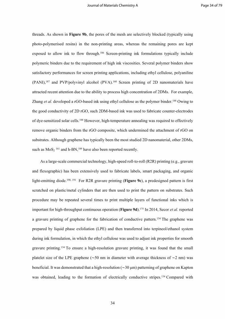
Screen printing is a template-based process whereby ink is transferred onto the substrate
through a stencil screen made of a fine, porous mesh of fabric, silk, synthetic fibres or metal
Page 33 of 79 Journal of Materials Chemistry A
34
threads. As shown in Figure 9b, the pores of the mesh are selectively blocked (typically using
photo-polymerised resins) in the non-printing areas, whereas the remaining pores are kept
exposed to allow ink to flow through.186 Screen-printing ink formulations typically include
polymeric binders due to the requirement of high ink viscosities. Several polymer binders show
satisfactory performances for screen printing applications, including ethyl cellulose, polyaniline
(PANI),187 and PVP/polyvinyl alcohol (PVA).160 Screen printing of 2D nanomaterials have
attracted recent attention due to the ability to process high concentration of 2DMs. For example,
Zhang et al. developed a rGO-based ink using ethyl cellulose as the polymer binder.188 Owing to
the good conductivity of 2D rGO, such 2DM-based ink was used to fabricate counter-electrodes
of dye-sensitized solar cells.188 However, high-temperature annealing was required to effectively
remove organic binders from the rGO composite, which undermined the attachment of rGO on
substrates. Although graphene has typically been the most studied 2D nanomaterial, other 2DMs,
such as MoS2 161 and h-BN,189 have also been reported recently.
As a large‐scale commercial technology, high-speed roll-to-roll (R2R) printing (e.g., gravure
and flexographic) has been extensively used to fabricate labels, smart packaging, and organic
light-emitting diode.190, 191 For R2R gravure printing (Figure 9c), a predesigned pattern is first
scratched on plastic/metal cylinders that are then used to print the pattern on substrates. Such
procedure may be repeated several times to print multiple layers of functional inks which is
important for high‐throughput continuous operation (Figure 9d).175 In 2014, Secor et al. reported
a gravure printing of graphene for the fabrication of conductive pattern.134 The graphene was
prepared by liquid phase exfoliation (LPE) and then transferred into terpineol/ethanol system
during ink formulation, in which the ethyl cellulose was used to adjust ink properties for smooth
gravure printing.134 To ensure a high-resolution gravure printing, it was found that the small
platelet size of the LPE graphene (∼50 nm in diameter with average thickness of ∼2 nm) was
beneficial. It was demonstrated that a high-resolution (∼30 μm) patterning of graphene on Kapton
was obtained, leading to the formation of electrically conductive stripes.134 Compared with
Page 34 of 79Journal of Materials Chemistry A

35
gravure printing, flexographic printing takes a slightly more complex ink transfer process. To
form graphic patterns, soft and flexible relief printing plates are mounted onto a plate cylinder.
Ink is first applied to the surface of a screened anilox roller, which is rolled through an ink trough
to fill the cells with ink. Unlike gravure printing, the cells of anilox roller are not the graphic-
forming part and are used primarily for metering the amount of ink to ensure continuous patterns.
Baker et al. demonstrated the flexographic printing of graphene in 2014.133 A graphene/sodium
carboxymethylcellulose ink was first formulated in water/IPA solutions, and then printed on
indium tin oxide (ITO) glasses to prepare counter-electrodes for photovoltaics. The
graphene/polymer binder ratio was controlled to suit flexographic printing.133
The various types of 2D printing techniques offer a straightforward, flexible, and cost-
effective solution for the fast fabrication of functional devices with satisfactory resolution. Owing
to the continuous operation and high printing efficiency, 2D flexographic printing and gravure
printing have shown tremendous potential for large-scale manufacturing of electronic circuits and
sensors. However, the printing of bulk 3D devices using conventional 2D printing techniques
remains a challenge.
4.2. 3D printing
Since its conception from 1980s, three-dimensional printing has gained unprecedented levels
of interests from academic community as well as industry, leading to inestimable possibilities for
fast prototyping. The 3D printing begins with the formation of a virtual model, followed by the
deposition/polymerization of starting materials, and post-treatment of the printed objects. 3D-
printing technologies are commonly grouped into following major categories:4 (1) material jetting
(e.g. inkjet printing), (2) extrusion/micro-extrusion (e.g. direct ink writing), (3)
photopolymerization, (4) powder-bed fusion, and (5) lamination. Herein, we will only discuss
mostly used methods for additive 3D printing of colloidal 2D materials, which are (1) and (2).
Comprehensive review of 3D printing can be found in other recent literatures.7, 151
Page 35 of 79 Journal of Materials Chemistry A

36
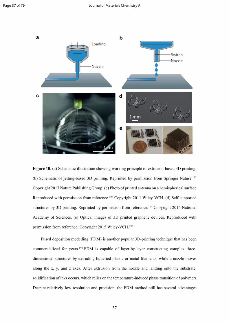
Direct ink writing (DIW) and inkjet printing are arguably two most prevalent strategies for
3D printing of colloidal nanoparticles because of its straightforward procedure, cost effectiveness,
flexible choice of materials, and ability to construct highly sophisticated 3D structures without
additional masking requirements.5 After being extruded under an external pressure (Figure 10a)
or ejected in form of droplets by nozzles (Figure 10b), the inks solidify to form 3D objects either
through gelation, phase transition, or simply solvent evaporation.20 The printing resolution of the
direct ink writing is normally determined by the size of printing nozzles, and various predesigned
substrates may be used during DIW, such as hemispherical antennas (Figure 10c), suggesting
broad utility in electronics and optoelectronics.192, 193 One striking feature of DIW is the flexibility
of printable ink options that include not only shear-thinning nanoparticle dispersions, but also
exceedingly viscous hydrogels. Such advantage of DIW allows for an unrivalled freedom of
material choices and preparation of suitable inks.158, 194, 195 The viscoelastic properties of certain
inks have enabled self-supporting structures, such as 3D butterfly design (Figure 10d).194 As
early as 2015, García‐Tuñon et al.196 formulated GO inks that possessed good elastic shear
modulus to construct self‐supporting 3D structures via DIW (Figure 10e). After drying and
thermal reduction, an ultra‐light graphene device was obtained with elastomeric behavior and
decent conductivity.
Page 36 of 79Journal of Materials Chemistry A
37
Figure 10. (a) Schematic illustration showing working principle of extrusion-based 3D printing.
(b) Schematic of jetting-based 3D printing. Reprinted by permission from Springer Nature.197
Copyright 2017 Nature Publishing Group. (c) Photo of printed antenna on a hemispherical surface.
Reproduced with permission from reference.193 Copyright 2011 Wiley-VCH. (d) Self-supported
structures by 3D printing. Reprinted by permission from reference.194 Copyright 2016 National
Academy of Sciences. (e) Optical images of 3D printed graphene devices. Reproduced with
permission from reference. Copyright 2015 Wiley-VCH.196
Fused deposition modelling (FDM) is another popular 3D-printing technique that has been
commercialized for years.198 FDM is capable of layer-by-layer constructing complex three-
dimensional structures by extruding liquefied plastic or metal filaments, while a nozzle moves
along the x, y, and z axes. After extrusion from the nozzle and landing onto the substrate,
solidification of inks occurs, which relies on the temperature-induced phase transition of polymers.
Despite relatively low resolution and precision, the FDM method still has several advantages
Page 37 of 79 Journal of Materials Chemistry A

38
including easy operation and low operating costs.199 Among various types of polymer filaments,
poly(lactic acid) (PLA) and acrylonitrile-butadiene-styrene (ABS) are the two popular choices for
FDM. To date, FDM printing of nanocomposites including ABS/graphene,200 PLA/graphene,201
and PLA/LFP/carbon202 was reported. In preparation of filaments of PLA/graphene, rGO and
polylactic acid were blended at elevated temperature to form composite powders.169 After the
FDM printing, the obtained 2D and 3D flexible circuits showed good mechanical performance.
However, it is worth noting that high content of PLA (94 wt%) may lower the electrical
conductivity (476 S/m), whereas increasing the concentration of rGO or post-treatment (such as
thermal sintering) may mitigate this issue.
As discussed previously, inkjet and aerosol-jet printing are non-contact fabrication
techniques that were originally developed for 2D printing. However, these two printing
techniques can be redesigned for 3D printing purposes. Owing to their drop-on-demand
characteristics, inkjet printing and aerosol jet printing are promising solutions toward rapid and
economical deposition of inks on various substrates according to predesigned patterns.203 In 2017,
Panat’s group demonstrated highly intricate microscale 3D networks based on aerosol jet printing
techniques.164 Without using any supporting materials, sophisticated nanoarchitectures with
nearly fully dense truss elements, including microscaffolds as well as microlattices, were realized.
In the past decade, inkjet printing of 3D graphene aerogels or hydrogels has attracted enormous
interest and achieved some progresses.204 For instance, Chi et al. reported an inkjet
printable graphene/polyaniline (Gr-PANI) composite ink that was prepared by ball milling and
ultrasonication.167 Such 2DM-based ink was printed on freestanding graphene paper to form a
three-dimensional hybrid electrode. With good mechanical flexibility, the printed Gr-PANI and
gel electrolyte created an all-solid-state symmetric supercapacitor that showed a decent energy
density as well as high cycling durability.
Although various types of 2D nanomaterials have been successfully printed in the past
decade, the 3D printing of 2DMs has mainly focused on extrusion-based processes (e.g. direct ink
Page 38 of 79Journal of Materials Chemistry A

39
writing and fused deposition modelling). Innovative printing approaches are highly desirable to
expand the scope of printable 3D devices and to make full use of 2DMs functionalities, which
may lead to the development of intelligent structures that are multifunctional, adaptive, and
programmable.
4.3. 4D printing
The ability of some 3D fabricated materials to evolve in a predefined shape, pattern, and
structures over time has given rise to a new term called “4D printing”.205 However, not all 3D
printing technologies that generate active components such as printed flexible hinges are regarded
as 4D printing as they do not exhibit ‘smart’ behaviour such as self-folding, self-actuating and
shape changing.206 It has been suggested that some of the distinguishing features of 4D printing
involve fabricating a physical object using suitable additive manufacturing techniques, and laying
down successive layers of stimuli-responsive materials with varying properties.207 After printing
process, the object responses to stimuli from the natural environment or through human
intervention, leading to a physical/chemical change of state over time. The 4D printing with
shape-morphing features has been considered as a powerful paradigm for designing and
fabricating multi-functional hierarchical structures.208
Page 39 of 79 Journal of Materials Chemistry A

40
Figure 11. (a) Schematic showing working principle of 4D printing of hydrogel. Upon swelling,
the shape of printed hydrogel tends to deform to enable additional control of the final structure.
(b) Two hydrogel patterns with flower geometries and different petal patterns. Reprinted by
permission from Springer Nature.197, 209 Copyright 2016&2017 Nature Publishing Group. (c-e)
Dynamic expansion and contraction of MoS2 electrode. Reprinted by permission from Springer
Nature.210 Scale bar is 1 cm. Copyright 2017 Nature Publishing Group. (f) Photos of MoS2
composite hydrogels showing shape deformation and self-wrapping motions under remote control
of light or heat. Scale bar is 1 cm. Reprinted by permission from reference.211 Copyright 2016 The
Royal Society of Chemistry.
Page 40 of 79Journal of Materials Chemistry A

41
In the past few years, several research fields have emerged, including shape memory alloys
(SMAs),212 self-evolving structures,213 soft actuators/robotics,168, 214 active origami, and controlled
sequential folding.215 For example, 4D printing of hydrogel was demonstrated based on the
swelling ability of composite ink coupled with anisotropic design of printing patterns (Figure
11a).197, 209 Anisotropic swelling properties of different filament layers induced a controlled
deformation and curvature of printed hydrogels. Reversible changes in 3D shapes are feasible
with deswelling using external stimuli, such as heat. As shown in Figure 11b, several key factors
including printed patterns, the swelling ratios, and elastic moduli can be used to tailor the final
structural and properties of 4D-printed products. Theoretical mechanics models that expand the
classical Timoshenko theory can be useful guidelines for predicting and developing new 4D-
printed devices.216 In addition, hydrogels are able to be laminated against passive materials for
producing a self-evolving joint capable of twisting, curling, and folding upon swelling. 205, 213
Owing to the atomically thin structure and ultralow bending stiffness of 2D materials, many
of these 2DMs have huge potential for fabricating stimuli-responsive materials, which are the key
components for successful 4D printing.217 Acerce et al. showed that the dynamic expansion and
contraction of electrode films prepared by restacking exfoliated metallic MoS2 nanosheets can
produce considerable mechanical forces (Figure 11c-e).210 MoS2 electrode films can lift masses
that are more than 150 times that of the electrode in the scale of ~cm. Such actuation of MoS2 film
can be attributed to the suitable elastic modulus and good conductivity of the metallic 1T phase.
In addition to voltage response, Lei et al. reported a MoS2 composite hydrogel that showed
anisotropic actuation with thermo- and photo-responses. In this composite hydrogel, MoS2
worked as a photothermal transduction component, allowing for remote control of hydrogel
actuators (Figure 11f).211 The structural deformation and self-wrapping actions of the hydrogels
were demonstrated using light or heat as external stimuli.
Page 41 of 79 Journal of Materials Chemistry A
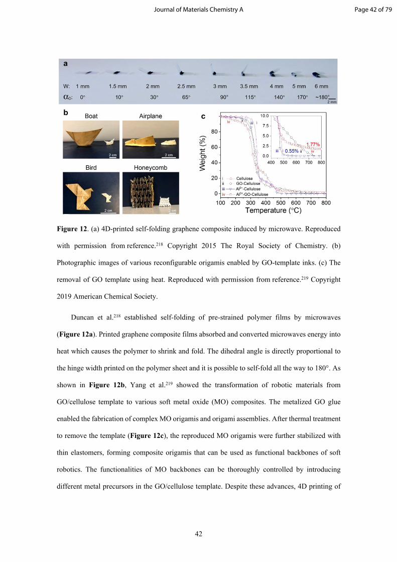
42
Figure 12. (a) 4D-printed self-folding graphene composite induced by microwave. Reproduced
with permission from reference.218 Copyright 2015 The Royal Society of Chemistry. (b)
Photographic images of various reconfigurable origamis enabled by GO-template inks. (c) The
removal of GO template using heat. Reproduced with permission from reference.219 Copyright
2019 American Chemical Society.
Duncan et al.218 established self-folding of pre-strained polymer films by microwaves
(Figure 12a). Printed graphene composite films absorbed and converted microwaves energy into
heat which causes the polymer to shrink and fold. The dihedral angle is directly proportional to
the hinge width printed on the polymer sheet and it is possible to self-fold all the way to 180°. As
shown in Figure 12b, Yang et al.219 showed the transformation of robotic materials from
GO/cellulose template to various soft metal oxide (MO) composites. The metalized GO glue
enabled the fabrication of complex MO origamis and origami assemblies. After thermal treatment
to remove the template (Figure 12c), the reproduced MO origamis were further stabilized with
thin elastomers, forming composite origamis that can be used as functional backbones of soft
robotics. The functionalities of MO backbones can be thoroughly controlled by introducing
different metal precursors in the GO/cellulose template. Despite these advances, 4D printing of
Page 42 of 79Journal of Materials Chemistry A

43
2D nanomaterials remains an underexplored avenue for the fabrication of multifunctional,
programmable, and smart structures/devices.
5. Device applications of printed 2D nanomaterials
Although significant development of 2DM-based devices has been seen in the past decade,
device applications based on additive manufacturing of 2D nanomaterials are only beginning to
emerge. This section provides a snapshot of some representative device applications based on
2DM printing, with an emphasis on energy and sensing devices.
5.1. Energy conversion and storage
The generation/storage of electric energy from sustainable sources, such as waste heat,
wind and sun light, is one of the pressing challenges for modern society in 21st century.220, 221 A
great number of energy technologies are emerging as possible solutions for bridging the gaps
between global energy supply and demand. Here, thermoelectrics, supercapacitors, batteries, and
solar cells are used as a few representative examples to illustrate potential energy applications of
additive printing using 2DMs.
5.1.1. Thermoelectrics
When it comes to global energy consumption and supply, sustainable energy is one of the
most crucial sources for securing long-term electricity supply. Thermoelectric (TE) materials
have gained huge attentions due to the ability to convert waste heat to electric energy.222-226
Printing techniques that rapidly transform thermoelectric inks into TE devices with predesigned
shapes have great potentials to accelerate practical applications of TE technology.227, 228 Up to
now, a great variety of TE materials ranging from inorganic nanoparticles (such as Bi2Te3, Sb2Te3,
Bi0.5Sb1.5Te3, Bi2Te2.7Se0.3, PbTe, Ca3Co4O9, etc.) to organic polymers (such as poly(3,4-
ethylenedioxythiophene) polystyrene sulfonate) have been successfully integrated in printing
techniques.130, 229-232 As printable 2D nanomaterials, few-layer graphene has been reported in
inkjet printing processes for fabricating flexible thermoelectric thin films (Figure 13a-c).233 The
Page 43 of 79 Journal of Materials Chemistry A

44
printed graphene films exhibit electrical transport akin to that of few‐layer graphene, and glassy
thermal transport originated from disordered nanostructures. The thermoelectric power factor of
the printed films is determined to be 18.7 ± 3.3 µW m−1 K−2. Such inkjet‐printed thermoelectric
devices confirmed the feasibility of low‐cost thermoelectric applications, allowing for the harvest
of electric energy from body heat in wearable applications.
Figure 13. Printable 2D materials for thermoelectric (TE) applications. (a) Schematic
demonstration of a thermoelectric device for power generation. Reproduced with permission
from reference.226 Copyright 2009 The Royal Society of Chemistry. (b) Printed flexible TE
devices. (c) Voltage output of Ag/graphene devices as a function of temperature gradient.
Page 44 of 79Journal of Materials Chemistry A

45
Reproduced with permission from reference.233 Copyright 2018 Wiley-VCH. (d) Screening
printing process of flexible TE films using Bi2Te2.8Se0.2 nanoplate ink. Reprinted by permission
from Springer Nature.129 Copyright 2016 Nature Publishing Group. (e) Photos of the printed TE
materials with different shapes. (f) Images of the printed conformal TE devices. (g) Output
voltage and power of the printed TE devices. Reprinted by permission from Springer Nature.123
Copyright 2018 Nature Publishing Group.
In addition to graphene, additive printing of other 2D nanomaterials have been reported.
For example, Zhang’s group demonstrated high-performance flexible films and devices by screen
printing bismuth telluride based nanoplate inks synthesized using a microwave-stimulated wet-
chemical method (Figure 13d).129 The films showed an unprecedented peak ZT of 0.43 at 175 °C
and superior flexibility with negligible changes of electrical conductivity after 150 bending cycles.
A flexible thermoelectric device fabricated using the printed films produces a high-power density
of 4.1 mW/cm2 under a temperature difference of 60 °C. A high-performance PbTe based flexible
film was also demonstrated by Zhang’s group by scalable and low-cost printing, with conservative
estimate of ZT above 1 at 350 °C.234 These high-performance and flexible thermoelectric devices
present an important step to make thermoelectrics a viable technology for a broad range of
applications.
Although significant efforts have been made in printable TE materials, the large-scale
applications of printed TE devices remain a challenge due to two main reasons: 1) The electrical
conductivity of the printed TE materials is often lower than their single-crystalline bulk
counterparts, leading to unsatisfactory output power and low figure-of-merit ZT values; 2)
conformal printing of TE devices on different shapes that can fit the geometries of heat sources,
such as hot pipelines, remains difficult. To address these issues, Kim et al. proposed a extrusion-
based 3D-printing approach to fabricate thermoelectric materials with geometries suitable for heat
sources.123 Bi2Te3-based TE materials were integrated with inorganic binders using Sb2Te3
chalcogenidometallate during ink formulation. After printing and sintering, various shapes of TE
Page 45 of 79 Journal of Materials Chemistry A

46
devices were obtained and readily integrated onto pipeline systems (Figure 13e-f). Homogenous
thermoelectric performance was observed in 3D-printed materials, of which the ZT values of 0.9
for p-type and 0.6 for n-type were comparable to their bulk counterparts. The TE devices showed
a maximum output voltage of 27.0 mV and maximum power of 1.62 mW at a temperature
difference of 39 °C (Figure 13g). In addition to extrusion-based 3D-printing methods, a 3D
conformal aerosol jet printing was demonstrated to deposit solution-processed Bi2Te2.7Se0.3
nanoplate inks onto both 2D planar and 3D curved substrates.235 Within seconds of photonic
sintering process, the electrical conductivity of the printed film was dramatically improved from
non-conductive to 2.7×10⁴ S/m. A power factor of 730 Wm-1K-2 was achieved for the printed
flexible films with good stability after 500 bending cycles.
5.1.2. Supercapacitors
Based on the double-layer effect, supercapacitors enable rapid charging and discharging
through the storage and release of electrical energy in a short period of time.236, 237 Owing to their
large specific surface area, 2D materials have emerged as encouraging candidates for developing
high-performance supercapacitors/ultracapacitors.14, 238, 239 For example, Pumera’s group and
Banks’ group have applied graphene/PLA into functional electrodes for supercapacitors through
fused deposition modelling printing.240, 241 In another example, the micro-extrusion 3D printing
method was effectively used for the fabrication of rGO-based micro-supercapacitors.242 The
printed GO films were first treated with hydrogen iodide (HI), followed by the deposition of
PVA–H2SO4 gel as the electrolyte. A capacitance of 41.8 F·cm−3 at 0.06 A·cm−3 was obtained for
the printed micro-supercapacitor. To further improve the capacity of supercapacitors, Jiang et al.
fabricated graphene aerogel microlattices with rich hierarchical pores and high electrical
conductivity.243 During the printing process, a facile ion‐induced gelation method was
demonstrated to directly print aerogel microlattices from GO-based ink (Figure 14a-c). Using
Ca2+ as ionic gelators, aqueous GO solution was transformed into printable gel ink, leading to the
Page 46 of 79Journal of Materials Chemistry A

47
formation of free‐standing 3D structures with programmable microlattices at ambient
conditions. The gravimetric capacitance (Cs) of supercapacitors is 213 F·g−1 at 0.5 A·g−1 and 183
F·g−1 at 100 A·g−1, and retains over 90% after 50000 cycles.
Figure 14. Printable 2D materials for supercapacitors. (a) 3D printing of graphene oxide into
supercapacitors. (b) Photographic image of a printed supercapacitor with microscopic porous
morphology (c) SEM image of a printed graphene supercapacitor. Scale bars of (b) and (c) are 5
mm and 500 µm, respectively. Reproduced with permission from reference.243 Copyright 2018
Wiley-VCH. (d) The fabrication of MXene-based supercapacitors by 3D printing and ink
transferring using stamps. (e) Photos of several MXene-based supercapacitors. Reproduced with
permission from reference.244 Copyright 2018 Wiley-VCH.
Page 47 of 79 Journal of Materials Chemistry A

48
In addition to graphene, other conductive 2D materials have also been investigated for
fabricating supercapacitors. Recently, Zhang et al. developed a stamping strategy to transform 2D
titanium carbide or carbonitride inks into supercapacitors.244 As shown in Figure 14d, this process
started with stamp fabrication by FDM method using PLA filaments. Next, the 3D-printed stamp
was covered with MXene inks (Ti3C2Tx or Ti3CNTx), and hard-pressed onto flexible substrates to
generate all-MXene supercapacitors. Several MXene-based micro-supercapacitors were rapidly
manufactured with a wide variety of designs (Figure 14e), which showed good cycle life (>10000
cycles) and excellent capability (capacitance retention of 82% at 800 μA·cm−2).
5.1.3. Batteries
Supercapacitors are ideal when a rapid charging is desirable to fill a short-term power
demand, while batteries are required to supply long-term electric energy. Thanks to the rapid
development of printing technologies, direct print of 2D nanomaterials has been increasingly
investigated for applications including Li–O2 batteries,245 Li–S batteries,246 and Na-ion
batteries.247 For example, graphene/PLA composites have been used in the rapid manufacturing
of 3D printed freestanding anodes for lithium-ion batteries.240, 248 In 2016, Hu’s group developed
a fully 3D‐printed lithium‐ion battery by additive printing of GO‐based inks as well as gel
polymer electrolyte (Figure 15).136 Lithium titanium oxide (Li4Ti5O12, LTO) and lithium iron
phosphate (LiFePO4, LFP) were added into anode and cathode materials, respectively. The
3D‐printed LTO anode and LFP cathode showed stable cycling performance with specific
capacities of ≈170 mA g−1 and ≈160 mA·h·g−1, respectively. A fully 3D‐printed cell presented a
high electrode mass loading of 18 mg·cm−2 when normalized to the overall area of the battery.
The full cell delivered initial charge and discharge capacities of 117 and 91 mA·h·g−1. In 2018,
the same group described the use of holey graphene oxide (hGO) for 3D printing of lithium–
oxygen battery without the use of additives or binders.245 The 3D printed hGO meshes exhibited
hierarchical porosity: nanoscale (4–25 nm holes on hGO), microscale (~10 µm pores introduced
by lyophilization), and macroscale (<500 µm square pores of the mesh). The 3D printed mesh's
Page 48 of 79Journal of Materials Chemistry A

49
multi-level porosities improved active‐site utilization as well as mass/ionic transport, leading to
enhanced performance of Li–O2 battery performance in comparison with vacuum filtration
method. In order to explore the role of hierarchical porosity, specifically nanoporosity, on
electrochemical performance, GO nanosheets without nanoholes were prepared and compared
with regards to their performance in battery. The mesh cathodes of hGO outperformed that of
conventional GO under the full discharge condition, and showed better cycling depth and stability.
Figure 15. Printable 2D materials for batteries. (a) Schematic illustration of the 3D‐printed battery
electrodes as well as the electrolyte. (b) Photos of LFP/GO and LTO/GO inks. (c) Digital image
displaying the printing process. (d) Optical images of 3D‐printed interdigitated electrodes.
Reproduced with permission from reference.136 Copyright 2016 Wiley-VCH.
5.1.4. Solar cells
Owing to the extraordinary optical and electrical properties, several colloidal
nanoparticles (e.g. graphene) have been widely used in various solar cell systems including
heterojunction solar cells (HSCs),249 organic solar cells (OSC),250 dye/QDs sensitized solar cells
(DSSCs),251, 252 and perovskite solar cells (PSCs).253-256 For example, Hashmi et al . developed
inkjet infiltrated carbon-based printed perovskite solar cells with high stability and
reproducibility.257 As shown in Figure 16a-e, the authors demonstrated that the perovskite
Page 49 of 79 Journal of Materials Chemistry A

50
precursor ink is highly stable, printable, and controllable, and can directly be used to fabricate
porous triple layered printed PSCs with a high overall conversion efficiency of 9.53% without the
need of hole transporting materials. Owing to its high conductivity, 2D MXene nanosheets were
used in silicon solar cells to form an Ohmic junction with n+‐Si (Figure 16f).258 The metallic
feature enabled MXene to effectively extract the photogenerated electrons from the active layer,
leading to a decrease in device contact resistance and the suppression of charge carrier
recombination. An improved open‐circuit voltage and a high short‐circuit current density were
observed with a maximum power conversion efficiency of 11.5%. Despite that spin/drop coating
was used for the majority of the photovoltaic works published in the literature to date, printing
techniques have emerged as a promising approach for fast prototyping and scalable manufacturing
of solar cells.259, 260 A wide range of materials including graphite,257 carbon nanotubes,261 and dye
molecules262 have been incorporated in the printing of solar cells. In particular, the printing of 2D
nanomaterials has been increasingly investigated in the past few years. For example, Hasan group
demonstrated the use of graphene ink for fabricating dye-sensitized solar cells.263 In the
fabrication of counter electrodes (CE), graphene ink showed good uniformity and consistency, as
shown in Figure 16g. The authors also investigated the use of different dyes including natural
dye extracts from Pennisetum glaucum, Hibiscus sabdariffa and Caesalpinia pulcherrima as well
as the synthetic ruthenium-based dye N719, showing a maximum performance of ∼3.0%
conversion efficiency (Figure 16h). The inkjet-printed graphene electrode provided a cost-
effective alternative, which has a material cost of only ∼2.7% of the equivalent solution processed
Pt-based electrodes. As another example of printed solar cells, MXene/CuSe nanosheets were
screen-printed onto graphite sheet to form a counter electrode in quantum dot-sensitized solar
cells.264 The authors combined the high electrical conductivity of MXene (Ti3C2) and rich active
sites of CuSe for polysulfide electrolyte reduction.264 Therefore, such 2D composite CE enabled
the photovoltaic device with an improved efficiency of 5.12%, which is higher than that of pristine
CuSe CE (3.47%) or pristine Ti3C2 CE (2.04%).
Page 50 of 79Journal of Materials Chemistry A

51
Figure 16. Printable colloidal nanomaterials for solar cells. (a-c) Demonstrations of inkjet-
printed patterns using stable perovskite precursor ink, including (a) logos, (b) quick response (QR)
code, (c) digital image. (d-e) The short circuit current density (Jsc) and efficiency (η) of PSCs by
adjusting the volume of printing perovskite precursor ink, leading to the precise tuning of
photovoltaic performance. Reproduced with permission from reference.257 Copyright 2011
Wiley-VCH. (f) Schematic illustration of MXene-based silicon solar cells. Reproduced with
permission from reference.258 Copyright 2019 Wiley-VCH. (g) Image of printed graphene
electrodes showing good printing consistency. (h) Current–Voltage characteristic curves of
graphene-based solar cells sensitized with different dyes (Natural tropical dye: extracts
from Pennisetum glaucum, Hibiscus sabdariffa and Caesalpinia pulcherrima. Synthetic dye:
N719). Reproduced with permission from reference.263 Copyright 2016 Elsevier B.V.
The printing of 2DM-based inks provides a versatile platform for the design and
development of a broad range of devices for energy conversion and storage. With suitable printing
methods, these energy devices can be printed on a wide variety of substrates, such as flexible and
Page 51 of 79 Journal of Materials Chemistry A

52
transparent films, adjusting the conventional stereotypes of energy conversion and storage using
rigid structures. More importantly, the printing technologies enable the energy devices with low
dimension, high resolution and short fabrication time, which would serve as power supplies for
the development of next-generation wearable electronics and sensors.
5.2. Sensing
The ability of 2DMs to respond to the environment with ultra-high surface sensitivity has
been demonstrated as key characteristics for sensing applications. Moreover, 2DMs’ exceptional
optical/electrical properties, combined with the structural robustness and flexibility, enable these
materials to be desired candidates for manufacturing next-generation sensors. Combined with
printing technologies, we will highlight recent advances in functional devices for sensing physical,
chemical, and biological stimuli/inputs.
5.2.1. Optoelectronic sensor
The fast-expanding market of optoelectronic devices, including photodetectors and UV
sensors, calls for innovative production of nanostructures from optoelectronic materials in a low-
cost, high-throughput, and large-scale fashion.19, 265 Printing is a versatile technology for
deposition of ink materials and an emerging tool toward fast prototyping and manufacturing of
optoelectronic sensors. As many optoelectronic sensors involve charge transfer or energy transfer
processes, the electronic structure of the 2DMs plays an essential role in developing functional
optoelectronics based on desired donor–acceptor pair. In particular, the versatility in the band
gaps of 2D materials provides enormous opportunities in the field of optoelectronics (Figure 17a).
Page 52 of 79Journal of Materials Chemistry A

53
Figure 17. Optoelectronic sensors based on printable 2D nanomaterials. (a) The electromagnetic
wave spectrum and the band gap ranges of different 2D nanomaterials. Reproduced with
permission from reference.266 Copyright 2017 National Academy of Sciences. (b-d) MoS2 based
phototransistors. Reproduced with permission from reference.267 Copyright 2017 American
Chemical Society. (e) In2Se3 thin‐film photodetectors with thickness of 41 nm. Reproduced with
permission from reference.40 Copyright 2018 Wiley-VCH. (f) Schematic illustration of printed
black phosphorus (BP) photodetector. (g) The BP/Graphene/Si heterostructure showing high
photoresponsivity to 1550 nm light. Reprinted by permission from Springer Nature.149 Copyright
2017 Nature Publishing Group.
Semiconducting TMDs and BP have attracted lots of attentions because of their tunable
band gaps as well as atomically thin structures. For example, Kim et al. reported a highly
transparent MoS2 phototransistor arrays on flexible polymer substrates by a drop-on-demand
inkjet-printing technique.267 To fabricate the phototransistor arrays, the MoS2 monolayers were
selectively patterned using reactive ion etching system with O2 plasma (Figure 17 b-c), followed
Page 53 of 79 Journal of Materials Chemistry A

54
by inkjet printing of electrodes and dielectric layers. As shown in Figure 17d, the
printed phototransistors showed good responsivity and detectivity in the range of 400 to 800 nm
wavelength. In addition to MoS2, solution-processable indium selenide (InSe) flakes were used
to fabricate photodetector with high photo responsivities (≈5 × 10⁷A W−1) that surpass previously
reported solution‐processed monolithic semiconductor photodetectors by three orders of
magnitude (Figure 17 e).40 The pristine InSe flakes were prepared by liquid-phase exfoliation in
surfactant‐free, dexoygenated co-solvent mixtures and the fabricated field-effect transistors by
vacuum filtration and electron‐beam lithography. Such solution‐based process possesses huge
potential for the scalable synthesis of InSe and its thin films, which showed excellent responsivity
for film-based photodetectors.
Recently, two-dimensional black phosphorus has drawn significant research attentions
owing to its unique structural and electrical properties.266 An inkjet-printable BP ink was
developed for fabricating hybrid photodetector.149 As shown in Figure 17f, printed BP was
combined with graphene/Si Schottky junction to fabricate optoelectronic devices. To avoid
possible oxidation or degradation in air, a layer of parylene-C was used to encapsulate the hybrid
structure. Under 450 nm light source, a photoresponsivity of up to 164 mA W−1 was observed.
Interestingly, owing to the layer-dependent bandgap of BP (0.3–2.0 eV), the device can also
respond to 1550 nm light (1.8 mA W−1 photoresponsivity), as showed in Figure 17g.
For graphene, MXene and other low band-gap 2DMs, they have also been extensively
studied as an electrical contact or a photoactive layer in optoelectronics. In addition, the good
solution processability of GO allows the fully inkjet printing for graphene-based photodetectors.
Manga et al. formulated an ionic solution ink by combining GO nanosheets with titanium
bis(ammonium lactate) dihydroxide (TBA), and printed the ink on coplanar graphene-based
electrodes, producing a fully inkjet-printed photodetector.268 Heterostructure
graphene/WS2/graphene junction was also utilized for photodetection.125 This heterostructure
device exhibited a photoresponsivity >1 mA W−1 (at 514 nm).
Page 54 of 79Journal of Materials Chemistry A

55
5.2.2. Chemical sensor
Recently, graphene, rGO, TMDs, and other 2D nanomaterials are emerging as active
constituents for electrochemical sensing due to their superior electrical conductivity, excellent
electrochemical properties, and large surface to volume ratios compared to traditional metal
oxides and conducting polymers.269-272 Printed 2DM chemical sensor was first reported in
2010, where inkjet printing of rGO platelets was achieved using aqueous surfactant‐supported
dispersions of rGO powder.273 Despite relatively low electrical conductivity (σ ≈15 S cm−1), the
rGO‐based chemical sensor was able to detect chemically aggressive vapours at the parts per
billion level using an air sample at room temperature. An increase in electrical conductivity was
observed when the rGO sensor was exposed to highly oxidizing vapours, while there was an
increase in resistance when it was exposed to organic vapours and reducing species, including
hexanes, CH3OH, and NH3. In addition to 2D printed sensors, 3D printing of reduced graphene
oxide nanowires was realized to detect the CO2 concentrations between 0.25% an 5% (Figure
18a-b).274 By accurately tuning the printing parameters, the authors fabricated 3D printed rGO
wires with complex features, demonstrating controlled deposition direction as well as deposition
positions. The 3D printing of 2DM-based nanowires show enormous potential to fabricate
components of electrochemical sensing devices such as flexible sensing transducers.274
Page 55 of 79 Journal of Materials Chemistry A

56
Figure 18. Printable 2D materials for chemical sensors. (a) 3D printing of reduced GO-based
wires. (b) rGO nanowires for CO2 sensing. Reproduced with permission from reference.274
Copyright 2015 Wiley-VCH. (c) Chemical sensors based on microprinted graphene–PS–graphene
microparticles. (d) Surface conductance of graphene–PS–graphene microparticle on detecting
gold nanoparticles and Zn2+. (e) Raman shift of graphene–PS–graphene microparticle on detecting
gold nanoparticles and Zn2+. Reprinted by permission from Springer Nature.275 Copyright 2018
Nature Publishing Group.
Recently, Strano group integrated micro-printing technique with CVD-grown 2D
materials to develop an “auto-perforation” technique that provides a means of spontaneous
assembly for surfaces composed of two-dimensional molecular scaffolds.275 This innovative
approach was based on controlled crack propagation in CVD-grown 2DM thin films, creating
microparticles with a pair of enveloping 2D layers. In their work, the authors showcased a
graphene–polystyrene–graphene (G-PS-G) microparticle which was used as a platform to detect
Page 56 of 79Journal of Materials Chemistry A

57
and monitor environmental stimuli. Such G-PS-G microparticles with amine groups can form
interaction with gold nanoparticles (Figure 18c), and those with nitrilotriacetic acid (NTA)
ligands can probe Zn2+ ions. Therefore, amine-modified devices revealed a significant increase in
the surface conductivity for sensing gold nanoparticles, whereas a huge reduction was witnessed
for the NTA-modified particles on Zn2+ exposure (Figure 18d). Raman shift of printed
microsensor was also observed upon these chemical stimuli (Figure 18e).
In addition, there is an increasing emphasis on two areas in chemical sensing: 1) real-time
monitoring; 2) ultrahigh-sensitivity detection.276 The real-time monitoring commonly relies on
non-covalent interactions of 2D nanomaterials that enable a quick response and a fast recovery
rate. Such non-covalent interactions, dependent on the type of analytes, include electrostatic force,
hydrogen bonding, π-π interaction, and etc. To detect the trace amount of pollutants, strategies
based on covalent linkages between analytes and 2D nanomaterials sometimes can be more
suitable. As it allows analytes immobilize on the surface and to be stable during the assay,
covalent linkages overcome the weakness of the supramolecular forces, particularly for
biomolecule systems. The careful engineering of surface chemistry of 2D materials and novel
designs enabled by printing techniques would be desirable to realize the next-generation high-
performance chemical sensors.
5.2.3. Biosensor
2D materials appear to be a promising carrier platform for biological recognition elements
owing to their high surface sensitivity and exceptional electronic property.277-279 To monitor
glucose levels in the interstitial fluid, Lipani et al.9 developed a path-selective, non-invasive,
transdermal glucose monitoring system by screen printing of graphene film, as shown in Figure
19a. It was suggested that glucose reacted with glucose oxidase to produce hydrogen peroxide,
which was detected by the electrochemical sensor. With an increased density of graphene-
decorating Pt nanoparticles, the limit of detection was improved to about 0.76 μM. The authors
also performed in vivo testing in which the glucose levels of healthy volunteers were monitored
Page 57 of 79 Journal of Materials Chemistry A

58
by two of the array’s pixel devices, during which lunch and a snack were ingested (Figure 19b).
The results showed well-matched readout values that provided further confidence in the
performance of the array.
Figure 19. Printable 2D materials for biosensors. (a) Schematic demonstration of glucose sensing
devices. A 3D electrochemical cell is formed by contacting the gel with Ag/AgCl (reference) and
Pt (counter) electrodes. (b) The in vivo testing in which the glucose levels of healthy volunteers
were monitored. Reprinted by permission from Springer Nature.9 Copyright 2018 Nature
Publishing Group. (c-d) MoS2-based biosensor on detecting the chikungunya virus DNA under
the pH effect (c) and temperature effect (d). Reprinted by permission from Springer Nature.280
In addition to graphene, other 2D materials have been extensively investigated for
printable biosensors, particularly MoS2.281-283 Recently, Singhal et al. developed a biosensor based
on MoS2 nanosheets for the selective detection of chikungunya virus.280 Owing to MoS2’s
exceptional biocompatibility, good electrochemical activity, and high specific surface, the
biosensor exhibited a wide linear range of 0.1 nM to 100 µM towards the chikungunya virus DNA.
Page 58 of 79Journal of Materials Chemistry A

59
The biosensor also showed low limit of detection with 3.4 nM in a 3σ rule. As shown in Figure
19c-d, the pH response and temperature effect of the biosensor were studied, showing highest
current response at 7.8 pH and 35 °C.
5.2.4. Other sensors
The rapid development of printing technology has enabled many other sensing and
monitoring systems, such as temperature sensors, pressure gauges, and humidity detectors. Based
on solution-processable colloidal nanoparticles, several printed temperature sensors have been
demonstrated, showing strong potential in various research and industrial processes.284-286 Due to
the excellent electrical, mechanical, and thermal properties, graphene and its derivatives have
been widely used in developing sensors for temperature probing and monitoring.287-289 For
example, a flexible resistive temperature sensor was inkjet-printed using graphene/PEDOT:PSS
ink.290 The sensing device showed a negative temperature dependence of resistance with 0.06%
per degree Celsius sensitivity. Very recently, Zhao et al. developed a printed tandem line-type
temperature sensors based on reduced graphene oxide.289 The authors also used DIW printing
method to fabricate MXenes/CNTs positive electrode and rGO/CNTs negative electrode, which
were used as a supercapacitor to power the temperature sensors. The authors found that the
temperature sensitivity of the printed integrated electronic device can reach 1.2% per degree
Celsius in resistance.
Owing to 2D nanomaterials’ exceptional mechanical properties and ultrathin thicknesses,
they are emerging as attractive platform for strain sensors.291-294 In a typical printed strain sensor,
a conductive pattern can respond to geometric deformation that changes one or several key
parameters of the sensor, such as resistance or capacitance.295-297 Casiraghi et al. reported inkjet
printed strain gauges based on liquid-exfoliated graphene (Figure 20 a-c).166 By adjusting several
key printing parameters such as number of printing passes (Figure 20 d-e), gauge factor up to
125 was obtained, which led to high sensitivity (>20%) under small strains (0.3%). In another
recent study, 2D MXene has been used to develop a flexible pressure sensor with interdigital
Page 59 of 79 Journal of Materials Chemistry A

60
electrodes based on their change in d-spacing upon external pressure.10 An in situ transmission
electron microscopy study directly illustrated a decrease in interlayer distances under pressure
(Figure 20 f), providing a qualitative understanding of the working mechanism of MXene-based
sensor. A great range of pressure can be detected using the MXene-based piezoresistive sensor
with a decent gauge factor (GF ~ 180), good mechanical reversibility (over 4,000 times), and short
response time (<30 ms). The authors also demonstrated a MXene-based sensor pixel array (4 × 4)
for mapping the pressure distribution, as shown in Figure 20g-i. When an object (e.g. a watch)
was positioned on the sensor arrays, the corresponding output at each pixel was recorded and
measured, allowing for mapping local pressure distribution quantitatively.
Figure 20. (a) Schematic of the simple circuit for graphene strain sensor. (b-c) Graphene sensing
system under (b) tensile and (c) compressive strain. (d) Resistance as a function of the inverse of
the bending radius and under different layer thicknesses. (e) Sensitivity as a function of 1/r under
different layers. Reproduced with permission from reference.166 Copyright 2018 Elsevier. (f) The
in situ dynamic monitoring of MXene under an external pressure, showing the change of
interlayer distance (scale bar is 40 nm). (g) 4 × 4 MXene-based sensor pixel arrays for sensing
pressure distribution (scale bar is 5 mm). (h) A watch was positioned on the arrays. (i) The
Page 60 of 79Journal of Materials Chemistry A

61
corresponding resistance change was evaluated at each pixel. Reprinted by permission from
Springer Nature.10 Copyright 2017 Nature Publishing Group.
Due to the ability to attract or interact with water molecules, numerous hydrophilic
nanomaterials have recently attracted research interest in humidity sensing279, 298 and water-level
monitoring.299, 300 Owing to the strong hydrophilic feature enabled by surface functional groups,
2DMs such as graphene oxides and MXene have been used in developing flexible/wearable
humidity sensors.301-304 For example, Yuan’s group developed a flexible humidity sensor based
on poly(3,4-ethylenedioxythiophene)/reduced graphene oxide/Au nanoparticles.298 Using inkjet
printing techniques, the thin-film humidity sensor showed high conductivity and sensitivity
with superior stability after 200 bending cycles. The sensor can respond to a wide range
of humidity (11%–98% relative humidity), while producing a wide resistance change of 7%–52%.
For some 2DMs (e.g., black phosphorus) of which the intrinsic conductivity is sensitive to
ambient water, humidity sensors can also be developed through rational device design.305-307 For
example, a thick-film black-phosphorus humidity sensor was fabricated with a high response to
humidity change.305 Such humidity-response property showed decent stability after 3-month
exposure to ambient condition with 25 % relative humidity. Compared with conventional thin-
film sensor, the authors suggested that a thick film of BP nanosheets can be more robust for long-
term humidity sensing in moderate humidity conditions.
6. Conclusion and Future Perspectives
In the past decade, colloidal nanoparticles have been extensively employed in a variety of
printing processes because of their unique properties. In this review, we summarized and
evaluated state-of-the-art progresses on colloidal nanoparticle synthesis, ink formulation and
printing and device applications, and suggested high-priority areas for future research. As a
perspective on possible future directions, we listed some emerging technologies and research
Page 61 of 79 Journal of Materials Chemistry A

62
topics that could be potentially leveraged in the development of next-generation printed functional
devices (Table 4).
Table 4: Examples of emerging trends of printing-related technologies and their applications in
functional devices.
Emerging fields Capabilities & Features Example Applications
Reference
Ink formulation
Orientation engineering
Ink particles can self-assemble or be direct-assembled into functional structures with high orientational ordering
Ordered/aligned devices
[320,321]
Nanosurfactant QD nanosurfactants stabilize graphene in water with high colloidal stability
Photonic materials
[28]
Semiconductor binder/solder
Connecting semiconductor particles under mild conditions
Thermoelectrics, FETs
[123,308]
Green solvent Providing a low hazard, and highly scalable method
Transistor [106]
Printing methodology
High throughput printing
A bar-coating technique (speed of 6 m min−1) enables large-area polymer circuits
Large-area electronics
[314]
Volumetric printing
Printing entire complex objects on a time scale of seconds
Custom objects [315,316]
Embedded printing Fabricating devices within extensible elastomeric matrices
Strain sensors [319]
Multi-material printing
Direct printing and mixing of multiple, high-quality materials by one printing process
Shape memory circuit
[317,318]
Substrate Surface coating Improve the printability of substrates
Microfluidics [148]
Prepatterned Providing a customizable platform for generating 1D/2D patterns
Microcontact printing
[22,144]
Smart substrate Thermo-responsive polymers were used as reversible shape changing substrates
Soft actuators [169]
Sintering/Annealing
Microwave annealing
Reduce GO into pristine graphene using 1- to 2-second pulses of microwaves
Hydrogen evolution
[325]
Photonic sintering Sintering of printed films on polymer substrates within seconds
Thermoelectrics [130]
Page 62 of 79Journal of Materials Chemistry A

63
The properties of 2D materials vary significantly, as expected from their diversity in
chemical/electronic structures, from zero/small band gaps for some materials (e.g. graphene,
MXene) to large band gaps for others (e.g. MoS2, h-BN). The rich diversity of 2D materials in
chemistry/physics offers numerous opportunities for formulating high-performance inks and
printing functional devices, but also presents challenges for comprehensive understanding of
specialized roles of 2DMs in printing process. The review considered four key aspects: 2D
material synthesis, ink formulation, printing processes, and device applications.
In the section of 2D material synthesis, the rapid development of nanoparticle synthesis
has accelerated progresses in preparing advanced 2D nanomaterials with controlled
nanostructures. By using bottom-up or top-down approaches, ultrathin 2D nanomaterials have
been synthesized with high yield and fast production speed. However, the commercial production
(e.g. 1~100 kg level) of high-performance 2D nanomaterials remains a major challenge. For
example, many LPE-based monolayer syntheses rely on ultrasonication for hours and even days,
which makes it challenging for large-scale manufacturing of 2DMs. Methods that can consistently
produce high-quality 2DMs with low cost and industrial scale are yet to be developed.
For processing inks, the ingredients (e.g. solvents, surfactants, and binders) play
significant roles in determining the quality of inks, and thus innovations in ink additives can
further improve the performance of printed devices. For example, the development of
composition-matched molecular “solders” has demonstrated considerable improvement in device
carrier mobility.308 In addition, surfactants can greatly reduce the interfacial tension and form
steric and/or provide electrostatic stabilization for 2D nanomaterials in inks. However, the residue
surfactant in printed devices often limits the overall functionalities of the 2D materials, which
requires post-treatments to remove the surfactant. Therefore, one practical need to the large-scale
applications of 2DM-based inks is the development of compatible ink additives such that they
wouldn’t compromise the performance of printed devices. A possible solution is to develop
semiconducting/conducting nano-surfactants that do not undermine or even improve the device
Page 63 of 79 Journal of Materials Chemistry A

64
functionalities of 2D materials. For instances, recent advances in colloidal nano-surfactants or so-
called Pickering surfactants have shown that quantum dots,28 graphene,309 MoS2,310 and 2D
clays311-313 can reduce surface tension and show “surfactancy” upon appropriate surface
functionalization of nanoparticles. This could be a promising approach for preparing organic-free
functional inks, and more works need to be done on this aspect.
In the past decade, the emergence of 2D/3D/4D printing has enabled rapid prototyping of
macroscale functional devices from nanoscale building blocks.314-320 Despite considerable
progresses, there is still much to be done on comprehensive understanding and further
optimization of ink rheological properties, drying process, and substrate-ink interactions. In
addition, the fundamental understanding of the effect of 2D structure and chemical characteristics
of 2DMs on above processes is critically important. As mentioned in Section 3.1, the colloidal
stability of 2D particles in fluids is fundamentally different from spherical nanoparticle, such as
the electrostatic repulsion energy and sedimentation rate. However, the impact of the unique
dimensionality of 2DMs on printing technology remains poorly understood. Another possible
direction to improve the overall performance of printed 2DMs is to design and develop novel
printing processes. For example, multi-materials printing that integrates two or more 2D
functional materials in situ during printing may enable fast prototyping and high-throughput
discovery of novel heterostructures or nanocomposites. Successful examples of heterogeneous
nanocompositing have been witnessed in the field of sensing. For instance, SnS2, WS2, MoS2, and
Ni3S2 have been adopted to enhance the performance of graphene/CNT based electrochemical
sensors.269-272
On the other hand, although significant efforts have been made in printing functional
devices, the electrical performance of printed 2D materials is often if not always lower than their
single-crystalline counterparts. In order to further improve the charge/energy carrier transport of
printed 2DM devices, methods that can align 2D materials with minimal defects are highly
desirable. To achieve high alignment, the liquid-crystalline assembly of 2D nanoparticles into
Page 64 of 79Journal of Materials Chemistry A
65
ordered structures seems to be a promising approach. As 2D materials are intrinsically anisotropic,
the dispersions of 2D particles have shown a fascinating diversity of liquid crystal phases, i.e.
forming orientationally or positionally ordered structures.321, 322 This approach, combined with
directed assembly tools, has been reported to significantly improve the device performance in
terms of thermal conductivity and electrical capacity,323, 324 and could be applicable to additive
printing processes. Innovative approaches of post-treatment (e.g. photonic sintering130 or
microwave treatment325) have also demonstrated great potential in improving the performance of
solution-processed nanoparticle films.
For device design and development, a wider selection of 2D materials should be included.
Newly-discovered 2D materials, including newly discovered tellurene and hematene,326, 327 have
not been fully characterized and may enable translational applications. These and other
undiscovered materials may have unprecedented properties that could hold the keys to new
research breakthroughs. To push forward the development of a new generation of printable
structures of 2D materials, it is of utmost importance to establish a fundamental structure-
processing-property relationship by innovative theoretical efforts, such as machine learning
method. For example, Rajan et al. developed machine-learning models to predict the band gap of
MXene using kernel ridge (KRR), support vector (SVR), Gaussian process (GPR), and bootstrap
aggregating regression algorithms.328 Theoretical/simulation works will be beneficial for better
understanding the ink behavior of 2D nanomaterials that governs their utility in device
applications.
Overall, unprecedented opportunities and challenges exist in printing colloidal
nanoparticles for functional systems and transforming vast number of nanomaterials into
next‐generation technologies in a scalable and economic fashion.
Page 65 of 79 Journal of Materials Chemistry A

66
AUTHOR INFORMATION
Corresponding Author
* Email: [email protected] (Y. Z.).
ACKNOWLEDGEMENTS
We acknowledge funding support from the National Science Foundation under award CMMI-
1747685, DARPA under DARPA HR00111820030, and U.S. Department of Energy under
awards DE-NE0008712 and DE-NE0008701.
Page 66 of 79Journal of Materials Chemistry A

67
References1. W. Zeng, L. Shu, Q. Li, S. Chen, F. Wang and X.-M. Tao, Adv Mater, 2014, 26, 5310-
5336.2. X. Wang, X. Lu, B. Liu, D. Chen, Y. Tong and G. Shen, Adv Mater, 2014, 26, 4763-
4782.3. K. Chen, W. Gao, S. Emaminejad, D. Kiriya, H. Ota, H. Y. Y. Nyein, K. Takei and A.
Javey, Adv Mater, 2016, 28, 4397-4414.4. A. Ambrosi and M. Pumera, Chem Soc Rev, 2016, 45, 2740-2755.5. K. Fu, Y. Yao, J. Dai and L. Hu, Adv Mater, 2017, 29.6. Z. Zhan, J. An, Y. Wei, V. T. Tran and H. Du, Nanoscale, 2017, 9, 965-993.7. A. Kamyshny and S. Magdassi, Chem Soc Rev, 2019, 48, 1712-1740.8. Z. Cui, Printed electronics: materials, technologies and applications, John Wiley &
Sons, 2016.9. L. Lipani, B. G. R. Dupont, F. Doungmene, F. Marken, R. M. Tyrrell, R. H. Guy and A.
Ilie, Nat Nanotechnol, 2018, 13, 504-511.10. Y. Ma, N. Liu, L. Li, X. Hu, Z. Zou, J. Wang, S. Luo and Y. Gao, Nature communications,
2017, 8, 1207.11. S. Borini, R. White, D. Wei, M. Astley, S. Haque, E. Spigone, N. Harris, J. Kivioja and
T. Ryhänen, ACS Nano, 2013, 7, 11166-11173.12. C. Tan, X. Cao, X.-J. Wu, Q. He, J. Yang, X. Zhang, J. Chen, W. Zhao, S. Han, G.-H.
Nam, M. Sindoro and H. Zhang, Chem Rev, 2017, 117, 6225-6331.13. Y. Liu, N. O. Weiss, X. Duan, H.-C. Cheng, Y. Huang and X. Duan, Nature Reviews
Materials, 2016, 1, 16042.14. V. Nicolosi, M. Chhowalla, M. G. Kanatzidis, M. S. Strano and J. N. Coleman, Science,
2013, 340, 1226419.15. L. Fu, H. Yang, A. Tang and Y. Hu, Nano Research, 2017, 10, 2782-2799.16. A. I. Khan and D. O’Hare, J Mater Chem, 2002, 12, 3191-3198.17. H. T. Li, R. H. Liu, W. Q. Kong, J. Liu, Y. Liu, L. Zhou, X. Zhang, S. T. Lee and Z. H.
Kang, Nanoscale, 2014, 6, 867-873.18. D. Chimene, D. L. Alge and A. K. Gaharwar, Adv Mater, 2015, 27, 7261-7284.19. M. Singh, H. M. Haverinen, P. Dhagat and G. E. Jabbour, Adv Mater, 2010, 22, 673-685.20. P. Chang, H. Mei, S. Zhou, K. G. Dassios and L. Cheng, Journal of Materials Chemistry
A, 2019, 7, 4230-4258.21. G. Hu, J. Kang, L. W. T. Ng, X. Zhu, R. C. T. Howe, C. G. Jones, M. C. Hersam and T.
Hasan, Chem Soc Rev, 2018, 47, 3265-3300.22. D. Tian, Y. Song and L. Jiang, Chem Soc Rev, 2013, 42, 5184-5209.23. Y. Q. Dong, J. W. Shao, C. Q. Chen, H. Li, R. X. Wang, Y. W. Chi, X. M. Lin and G. N.
Chen, Carbon, 2012, 50, 4738-4743.24. K. Hu, X. Xie, T. Szkopek and M. Cerruti, Chemistry of Materials, 2016, 28, 1756-1768.25. K. S. Novoselov, A. K. Geim, S. V. Morozov, D. Jiang, Y. Zhang, S. V. Dubonos, I. V.
Grigorieva and A. A. Firsov, Science, 2004, 306, 666-669.26. A. Geim and K. Novoselov, Nat Mater, 2007, 6, 183-191.27. D. C. Marcano, D. V. Kosynkin, J. M. Berlin, A. Sinitskii, Z. Z. Sun, A. Slesarev, L. B.
Alemany, W. Lu and J. M. Tour, ACS Nano, 2010, 4, 4806-4814.28. M. Zeng, S. A. Shah, D. Huang, D. Parviz, Y.-H. Yu, X. Wang, M. J. Green and Z. Cheng,
ACS applied materials & interfaces, 2017, 9, 30797-30804.29. Y. Peng, Z. Meng, C. Zhong, J. Lu, W. Yu, Z. Yang and Y. Qian, Journal of Solid State
Chemistry, 2001, 159, 170-173.30. Z. Huang, A. Zhou, J. Wu, Y. Chen, X. Lan, H. Bai and L. Li, Adv Mater, 2016, 28, 1703-
1708.31. Z. Tang, Z. Zhang, Y. Wang, S. C. Glotzer and N. A. Kotov, Science, 2006, 314, 274-
278.
Page 67 of 79 Journal of Materials Chemistry A

68
32. D. J. Late, B. Liu, H. S. S. R. Matte, C. N. R. Rao and V. P. Dravid, Advanced Functional Materials, 2012, 22, 1894-1905.
33. Z. Lin, Y. Liu, U. Halim, M. Ding, Y. Liu, Y. Wang, C. Jia, P. Chen, X. Duan, C. Wang, F. Song, M. Li, C. Wan, Y. Huang and X. Duan, Nature, 2018, 562, 254-258.
34. J. Zheng, H. Zhang, S. Dong, Y. Liu, C. Tai Nai, H. Suk Shin, H. Young Jeong, B. Liu and K. Ping Loh, Nature communications, 2014, 5, 2995.
35. B. Huo, B. Liu, T. Chen, L. Cui, G. Xu, M. Liu and J. Liu, Langmuir, 2017, 33, 10673-10678.
36. Y. Kubota, K. Watanabe, O. Tsuda and T. Taniguchi, Science, 2007, 317, 932-934.37. C. Lee, Q. Li, W. Kalb, X.-Z. Liu, H. Berger, R. W. Carpick and J. Hone, Science, 2010,
328, 76-80.38. Y. Lin, T. V. Williams, T.-B. Xu, W. Cao, H. E. Elsayed-Ali and J. W. Connell, The
Journal of Physical Chemistry C, 2011, 115, 2679-2685.39. J. D. Wood, S. A. Wells, D. Jariwala, K.-S. Chen, E. Cho, V. K. Sangwan, X. Liu, L. J.
Lauhon, T. J. Marks and M. C. Hersam, Nano letters, 2014, 14, 6964-6970.40. J. Kang, S. A. Wells, V. K. Sangwan, D. Lam, X. Liu, J. Luxa, Z. Sofer and M. C. Hersam,
Adv Mater, 2018, 30, 1802990.41. X. Zhang, P. Yu, H. Zhang, D. Zhang, X. Sun and Y. Ma, Electrochimica Acta, 2013, 89,
523-529.42. M. Liu, P.-Y. Chen and R. H. Hurt, Adv Mater, 2018, 30, 1705080.43. A. A. AbdelHamid, J. H. Soh, Y. Yu and J. Y. Ying, Nano Energy, 2018, 44, 399-410.44. R. Cai, D. Yang, K.-T. Lin, Y. Lyu, B. Zhu, Z. He, L. Zhang, Y. Kitamura, L. Qiu, X.
Chen, Y. Zhao, Z. Chen and W. Tan, J Am Chem Soc, 2019, 141, 1725-1734.45. X. Rui, Z. Lu, H. Yu, D. Yang, H. H. Hng, T. M. Lim and Q. Yan, Nanoscale, 2013, 5,
556-560.46. X. Xiao, H. Yu, H. Jin, M. Wu, Y. Fang, J. Sun, Z. Hu, T. Li, J. Wu, L. Huang, Y. Gogotsi
and J. Zhou, ACS Nano, 2017, 11, 2180-2186.47. M. Naguib, O. Mashtalir, J. Carle, V. Presser, J. Lu, L. Hultman, Y. Gogotsi and M. W.
Barsoum, ACS Nano, 2012, 6, 1322-1331.48. Z. P. Xu and G. Q. Lu, Chemistry of Materials, 2005, 17, 1055-1062.49. Y. Kuroda, K. Ito, K. Itabashi and K. Kuroda, Langmuir, 2011, 27, 2028-2035.50. S. Gao, Y. Lin, X. Jiao, Y. Sun, Q. Luo, W. Zhang, D. Li, J. Yang and Y. Xie, Nature,
2016, 529, 68.51. B. Mahler, V. Hoepfner, K. Liao and G. A. Ozin, J Am Chem Soc, 2014, 136, 14121-
14127.52. W. Mai, Y. Zuo, X. Zhang, K. Leng, R. Liu, L. Chen, X. Lin, Y. Lin, R. Fu and D. Wu,
Chem Commun, 2019, 55, 10241-10244.53. T. Yu, B. Lim and Y. N. Xia, Angew. Chem., Int. Ed., 2010, 49, 4484.54. X. Huang, S. Li, Y. Huang, S. Wu, X. Zhou, S. Li, C. L. Gan, F. Boey, C. A. Mirkin and
H. Zhang, Nature Communications, 2011, 2, 292.55. W. Cheng, J. He, T. Yao, Z. Sun, Y. Jiang, Q. Liu, S. Jiang, F. Hu, Z. Xie, B. He, W. Yan
and S. Wei, J Am Chem Soc, 2014, 136, 10393-10398.56. X.-J. Wu, X. Huang, X. Qi, H. Li, B. Li and H. Zhang, Angewandte Chemie International
Edition, 2014, 53, 8929-8933.57. P. Simon, L. Bahrig, I. A. Baburin, P. Formanek, F. Roder, J. Sickmann, S. G. Hickey,
A. Eychmuller, H. Lichte, R. Kniep and E. Rosseeva, Adv. Mater., 2014, 26, 3042.58. Z. Wu, J. Liu, Y. Li, Z. Cheng, T. Li, H. Zhang, Z. Lu and B. Yang, ACS Nano, 2015, 9,
6315-6323.59. S. Acharya, B. Das, U. Thupakula, K. Ariga, D. D. Sarma, J. Israelachvili and Y. Golan,
Nano letters, 2013, 13, 409-415.60. J. Niu, D. Wang, H. Qin, X. Xiong, P. Tan, Y. Li, R. Liu, X. Lu, J. Wu and T. Zhang,
Nature Communications, 2014, 5, 3313.
Page 68 of 79Journal of Materials Chemistry A

69
61. K. S. Novoselov, A. K. Geim, S. V. Morozov, D. Jiang, Y. Zhang, S. V. Dubonos, I. V. Grigorieva and A. A. Firsov, Science, 2004, 306, 666.
62. K. S. Novoselov, A. K. Geim, S. V. Morozov, D. Jiang, M. I. Katsnelson, I. V. Grigorieva, S. V. Dubonos and A. A. Firsov, Nature, 2005, 438, 197.
63. K. S. Novoselov, D. Jiang, F. Schedin, T. J. Booth, V. V. Khotkevich, S. V. Morozov and A. K. Geim, Proc. Natl. Acad. Sci. U. S. A., 2005, 102, 10451.
64. A. K. Geim and K. S. Novoselov, Nat. Mater., 2007, 6, 183.65. H. Li, J. Wu, Z. Yin and H. Zhang, Accounts Chem Res, 2014, 47, 1067-1075.66. V. Goyal, D. Teweldebrhan and A. A. Balandin, Appl Phys Lett, 2010, 97, 133117.67. P. Ares, F. Aguilar-Galindo, D. Rodríguez-San-Miguel, D. A. Aldave, S. Díaz-Tendero,
M. Alcamí, F. Martín, J. Gómez-Herrero and F. Zamora, Adv Mater, 2016, 28, 6332-6336.
68. Y. Huang, E. Sutter, N. N. Shi, J. Zheng, T. Yang, D. Englund, H. J. Gao and P. Sutter, ACS Nano, 2015, 9, 10612.
69. Y. Hernandez, V. Nicolosi, M. Lotya, F. M. Blighe, Z. Sun, S. De, I. T. McGovern, B. Holland, M. Byrne and Y. K. Gun’Ko, Nat. Nanotechnol., 2008, 3, 563.
70. L. X. Xu, J. W. McGraw, F. Gao, M. Grundy, Z. B. Ye, Z. Y. Gu and J. L. Shepherd, J. Phys. Chem. C, 2013, 117, 10730.
71. A. O’neill, U. Khan, P. N. Nirmalraj, J. Boland and J. N. Coleman, J. Phys. Chem. C, 2011, 115, 5422.
72. J. N. Coleman, M. Lotya, A. O’Neill, S. D. Bergin, P. J. King, U. Khan, K. Young, A. Gaucher, S. De and R. J. Smith, Science, 2011, 331, 568.
73. J. Kim, S. Kwon, D.-H. Cho, B. Kang, H. Kwon, Y. Kim, S. O. Park, G. Y. Jung, E. Shin, W.-G. Kim, H. Lee, G. H. Ryu, M. Choi, T. H. Kim, J. Oh, S. Park, S. K. Kwak, S. W. Yoon, D. Byun, Z. Lee and C. Lee, Nature communications, 2015, 6, 8294.
74. X. Dong, Y. Shi, Y. Zhao, D. Chen, J. Ye, Y. Yao, F. Gao, Z. Ni, T. Yu, Z. Shen, Y. Huang, P. Chen and L.-J. Li, Physical Review Letters, 2009, 102, 135501.
75. M. Zhang, R. R. Parajuli, D. Mastrogiovanni, B. Dai, P. Lo, W. Cheung, R. Brukh, P. L. Chiu, T. Zhou and Z. Liu, Small, 2010, 6, 1100-1107.
76. D. Parviz, S. Das, H. S. T. Ahmed, F. Irin, S. Bhattacharia and M. J. Green, ACS Nano, 2012, 6, 8857-8867.
77. A. Ciesielski and P. Samorì, Chem Soc Rev, 2014, 43, 381-398.78. S. Eigler and A. Hirsch, Angewandte Chemie International Edition, 2014, 53, 7720-7738.79. Y. T. Liang and M. C. Hersam, J. Am. Chem. Soc., 2010, 132, 17661.80. R. J. Smith, P. J. King, M. Lotya, C. Wirtz, U. Khan, S. De, A. O’Neill, G. S. Duesberg,
J. C. Grunlan and G. Moriarty, Adv. Mater., 2011, 23, 3944.81. G. Guan, S. Zhang, S. Liu, Y. Cai, M. Low, C. P. Teng, I. Y. Phang, Y. Cheng, K. L.
Duei and B. M. Srinivasan, J. Am. Chem. Soc., 2015, 137, 6152.82. P. May, U. Khan, J. M. Hughes and J. N. Coleman, J. Phys. Chem. C, 2012, 116, 11393.83. K. R. Paton, E. Varrla, C. Backes, R. J. Smith, U. Khan, A. O’Neill, C. Boland, M. Lotya,
O. M. Istrate and P. King, Nat. Mater., 2014, 13, 624.84. E. Varrla, C. Backes, K. R. Paton, A. Harvey, Z. Gholamvand, J. McCauley and J. N.
Coleman, Chemistry of Materials, 2015, 27, 1129-1139.85. D. Voiry, A. Mohite and M. Chhowalla, Chem Soc Rev, 2015, 44, 2702-2712.86. L. Niu, M. Li, X. Tao, Z. Xie, X. Zhou, A. P. A. Raju, R. J. Young and Z. Zheng,
Nanoscale, 2013, 5, 7202-7208.87. X. Fan, W. Peng, Y. Li, X. Li, S. Wang, G. Zhang and F. Zhang, Adv. Mater., 2008, 20,
4490.88. K. Erickson, R. Erni, Z. Lee, N. Alem, W. Gannett and A. Zettl, Adv. Mater., 2010, 22,
4467.89. X. Huang, X. Qi, F. Boey and H. Zhang, Chem Soc Rev, 2012, 41, 666-686.90. M. Naguib, V. N. Mochalin, M. W. Barsoum and Y. Gogotsi, Adv. Mater., 2014, 26, 992.
Page 69 of 79 Journal of Materials Chemistry A

70
91. X. Wang, S. Kajiyama, H. Iinuma, E. Hosono, S. Oro, I. Moriguchi, M. Okubo and A. Yamada, Nat. Commun., 2015, 6, 6544.
92. J. Halim, S. Kota, M. R. Lukatskaya, M. Naguib, M. Q. Zhao, E. J. Moon, J. Pitock, J. Nanda, S. J. May, Y. Gogotsi and M. W. Barsou, Adv. Funct. Mater., 2016, 26, 3118.
93. P. Urbankowski, B. Anasori, T. Makaryan, D. Er, S. Kota, P. L. Walsh, M. Zhao, V. B. Shenoy, M. W. Barsouma and Y. Gogotsi, Nanoscale, 2016, 8, 11385.
94. B. Anasori, Y. Xie, M. Beidaghi, J. Lu, B. Hosler, L. Hultman, P. Kent, Y. Gogotsi and M. W. Barsoum, ACS Nano, 2015, 9, 9507.
95. K. Sano, Y. S. Kim, Y. Ishida, Y. Ebina, T. Sasaki, T. Hikima and T. Aida, Nature Communications, 2016, 7, 12559.
96. I. Chowdhury, M. C. Duch, N. D. Mansukhani, M. C. Hersam and D. Bouchard, Environmental Science & Technology, 2013, 47, 6288-6296.
97. G. R. Wiese and T. W. Healy, Transactions of the Faraday Society, 1970, 66, 490-499.98. T. Missana and A. Adell, J Colloid Interf Sci, 2000, 230, 150-156.99. P. He, A. F. Mejia, Z. D. Cheng, D. Z. Sun, H. J. Sue, D. S. Dinair and M. Marquez, Phys
Rev E, 2010, 81.100. X. Sun, D. Luo, J. Liu and D. G. Evans, ACS Nano, 2010, 4, 3381-3389.101. J. I. Paredes, S. Villar-Rodil, A. Martínez-Alonso and J. M. D. Tascón, Langmuir, 2008,
24, 10560-10564.102. M. Bystrzejewski, A. Huczko and H. Lange, Materials Chemistry and Physics, 2008,
107, 322-327.103. J. N. Coleman, M. Lotya, A. O’Neill, S. D. Bergin, P. J. King, U. Khan, K. Young, A.
Gaucher, S. De, R. J. Smith, I. V. Shvets, S. K. Arora, G. Stanton, H.-Y. Kim, K. Lee, G. T. Kim, G. S. Duesberg, T. Hallam, J. J. Boland, J. J. Wang, J. F. Donegan, J. C. Grunlan, G. Moriarty, A. Shmeliov, R. J. Nicholls, J. M. Perkins, E. M. Grieveson, K. Theuwissen, D. W. McComb, P. D. Nellist and V. Nicolosi, Science, 2011, 331, 568-571.
104. G. Cunningham, M. Lotya, C. S. Cucinotta, S. Sanvito, S. D. Bergin, R. Menzel, M. S. P. Shaffer and J. N. Coleman, ACS Nano, 2012, 6, 3468-3480.
105. Y. Hernandez, M. Lotya, D. Rickard, S. D. Bergin and J. N. Coleman, Langmuir, 2010, 26, 3208-3213.
106. B. Schmatz, A. W. Lang and J. R. Reynolds, Advanced Functional Materials, 2019, DOI: 10.1002/adfm.201905266.
107. K.-G. Zhou, N.-N. Mao, H.-X. Wang, Y. Peng and H.-L. Zhang, Angewandte Chemie International Edition, 2011, 50, 10839-10842.
108. M. Yi, Z. Shen, S. Ma and X. Zhang, Journal of Nanoparticle Research, 2012, 14, 1003.109. X. Li, Y. Qin, C. Liu, S. Jiang, L. Xiong and Q. Sun, Food Chem, 2016, 199, 356-363.110. J. K. Lim, S. A. Majetich and R. D. Tilton, Langmuir, 2009, 25, 13384-13393.111. A. Gupta, V. Arunachalam and S. Vasudevan, The Journal of Physical Chemistry Letters,
2015, 6, 739-744.112. S. G. Hashmi, T. Moehl, J. Halme, Y. Ma, T. Saukkonen, A. Yella, F. Giordano, J. D.
Decoppet, S. M. Zakeeruddin, P. Lund and M. Grätzel, Journal of Materials Chemistry A, 2014, 2, 19609-19615.
113. R. J. Smith, P. J. King, M. Lotya, C. Wirtz, U. Khan, S. De, A. O'Neill, G. S. Duesberg, J. C. Grunlan, G. Moriarty, J. Chen, J. Wang, A. I. Minett, V. Nicolosi and J. N. Coleman, Adv Mater, 2011, 23, 3944-3948.
114. R. C. T. Howe, R. I. Woodward, G. Hu, Z. Yang, E. J. R. Kelleher and T. Hasan, Phys. Status Solidi B, 2016, 253, 911-917.
115. J. N. Coleman, Adv Funct Mater, 2009, 19, 3680-3695.116. T. Hasan, F. Torrisi, Z. Sun, D. Popa, V. Nicolosi, G. Privitera, F. Bonaccorso and A. C.
Ferrari, physica status solidi (b), 2010, 247, 2953-2957.117. P. K. Misra, B. K. Mishra and G. B. Behera, Colloids and Surfaces, 1991, 57, 1-10.118. S. G. Hashmi, M. Ozkan, J. Halme, K. D. Misic, S. M. Zakeeruddin, J. Paltakari, M.
Grätzel and P. D. Lund, Nano Energy, 2015, 17, 206-215.
Page 70 of 79Journal of Materials Chemistry A
71
119. T. Hasan, Z. Sun, F. Wang, F. Bonaccorso, P. H. Tan, A. G. Rozhin and A. C. Ferrari, Adv Mater, 2009, 21, 3874-3899.
120. L. Guardia, M. J. Fernández-Merino, J. I. Paredes, P. Solís-Fernández, S. Villar-Rodil, A. Martínez-Alonso and J. M. D. Tascón, Carbon, 2011, 49, 1653-1662.
121. A. Ciesielski, S. Haar, M. El Gemayel, H. Yang, J. Clough, G. Melinte, M. Gobbi, E. Orgiu, M. V. Nardi, G. Ligorio, V. Palermo, N. Koch, O. Ersen, C. Casiraghi and P. Samorì, Angewandte Chemie International Edition, 2014, 53, 10355-10361.
122. Y. T. Liang and M. C. Hersam, J Am Chem Soc, 2010, 132, 17661-17663.123. F. Kim, B. Kwon, Y. Eom, J. E. Lee, S. Park, S. Jo, S. H. Park, B.-S. Kim, H. J. Im, M.
H. Lee, T. S. Min, K. T. Kim, H. G. Chae, W. P. King and J. S. Son, Nature Energy, 2018, 3, 301-309.
124. J. Li, M. M. Naiini, S. Vaziri, M. C. Lemme and M. Östling, Advanced Functional Materials, 2014, 24, 6524-6531.
125. D. McManus, S. Vranic, F. Withers, V. Sanchez-Romaguera, M. Macucci, H. Yang, R. Sorrentino, K. Parvez, S.-K. Son, G. Iannaccone, K. Kostarelos, G. Fiori and C. Casiraghi, Nat Nanotechnol, 2017, 12, 343.
126. X. Ma, Z. Xie, Z. Yang, G. Zeng, M. Xue and X. Zhang, Materials Research Express, 2018, 6, 015025.
127. P. He, J. R. Brent, H. Ding, J. Yang, D. J. Lewis, P. O'Brien and B. Derby, Nanoscale, 2018, 10, 5599-5606.
128. W. Yang, J. Yang, J. J. Byun, F. P. Moissinac, J. Xu, S. J. Haigh, M. Domingos, M. A. Bissett, R. A. W. Dryfe and S. Barg, Adv Mater, 2019, 0, 1902725.
129. T. Varghese, C. Hollar, J. Richardson, N. Kempf, C. Han, P. Gamarachchi, D. Estrada, R. J. Mehta and Y. Zhang, Scientific Reports, 2016, 6, 33135.
130. M. Saeidi-Javash, W. Kuang, C. Dun and Y. Zhang, Advanced Functional Materials, 2019, 29, 1901930.
131. T. Carey, S. Cacovich, G. Divitini, J. Ren, A. Mansouri, J. M. Kim, C. Wang, C. Ducati, R. Sordan and F. Torrisi, Nature Communications, 2017, 8, 1202.
132. S. Santra, G. Hu, R. C. T. Howe, A. De Luca, S. Z. Ali, F. Udrea, J. W. Gardner, S. K. Ray, P. K. Guha and T. Hasan, Scientific Reports, 2015, 5, 17374.
133. J. Baker, D. Deganello, D. T. Gethin and T. M. Watson, Materials Research Innovations, 2014, 18, 86-90.
134. E. B. Secor, S. Lim, H. Zhang, C. D. Frisbie, L. F. Francis and M. C. Hersam, Adv Mater, 2014, 26, 4533-4538.
135. Y. Xu, M. G. Schwab, A. J. Strudwick, I. Hennig, X. Feng, Z. Wu and K. Müllen, Advanced Energy Materials, 2013, 3, 1035-1040.
136. K. Fu, Y. Wang, C. Yan, Y. Yao, Y. Chen, J. Dai, S. Lacey, Y. Wang, J. Wan, T. Li, Z. Wang, Y. Xu and L. Hu, Adv Mater, 2016, 28, 2587-2594.
137. G. Xiao, Y. Li, W. Shi, L. Shen, Q. Chen and L. Huang, Applied Surface Science, 2017, 404, 334-341.
138. G. Pangalos, J. M. Dealy and M. B. Lyne, Journal of Rheology, 1985, 29, 471-491.139. X. Yang, C. Guo, L. Ji, Y. Li and Y. Tu, Langmuir, 2013, 29, 8103-8107.140. D. Kleshchanok, M. Heinen, G. Nägele and P. Holmqvist, Soft Matter, 2012, 8, 1584-
1592.141. A. Goldschmidt and H.-J. Streitberger, BASF handbook on basics of coating technology,
William Andrew, 2003.142. C. B. Highley, C. B. Rodell and J. A. Burdick, Adv Mater, 2015, 27, 5075-5079.143. W. A. Zisman, in Contact Angle, Wettability, and Adhesion, American Chemical Society,
1964, vol. 43, ch. 1, pp. 1-51.144. G. Pariani, R. Castagna, L. Oggioni, L. Colella, A. Nardi, S. Anzani, C. Bertarelli and A.
Bianco, Advanced Materials Technologies, 2018, 3, 1700325.145. B. Xin and J. Hao, Chem Soc Rev, 2010, 39, 769-782.
Page 71 of 79 Journal of Materials Chemistry A

72
146. W.-K. Lee, W.-B. Jung, D. Rhee, J. Hu, Y.-A. L. Lee, C. Jacobson, H.-T. Jung and T. W. Odom, Adv Mater, 2018, 30, 1706657.
147. M. Zeng, P. Wang, J. Luo, B. Peng, B. Ding, L. Zhang, L. Wang, D. Huang, I. Echols, E. Abo Deeb, E. Bordovsky, C.-H. Choi, C. Ybanez, P. Meras, E. Situ, M. S. Mannan and Z. Cheng, ACS applied materials & interfaces, 2018, 10, 22793-22800.
148. T. Trantidou, Y. Elani, E. Parsons and O. Ces, Microsystems & Nanoengineering, 2017, 3, 16091.
149. G. Hu, T. Albrow-Owen, X. Jin, A. Ali, Y. Hu, R. C. T. Howe, K. Shehzad, Z. Yang, X. Zhu, R. I. Woodward, T.-C. Wu, H. Jussila, J.-B. Wu, P. Peng, P.-H. Tan, Z. Sun, E. J. R. Kelleher, M. Zhang, Y. Xu and T. Hasan, Nature communications, 2017, 8, 278.
150. P. G. Campbell, E. D. Miller, G. W. Fisher, L. M. Walker and L. E. Weiss, Biomaterials, 2005, 26, 6762-6770.
151. T. Jungst, W. Smolan, K. Schacht, T. Scheibel and J. Groll, Chem Rev, 2016, 116, 1496-1539.
152. H. Sirringhaus, T. Kawase, R. H. Friend, T. Shimoda, M. Inbasekaran, W. Wu and E. P. Woo, Science, 2000, 290, 2123-2126.
153. R. Cobas, S. Muñoz-Pérez, S. Cadogan, M. C. Ridgway and X. Obradors, Advanced Functional Materials, 2015, 25, 768-775.
154. R. E. Saunders and B. Derby, International Materials Reviews, 2014, 59, 430-448.155. D. Soltman and V. Subramanian, Langmuir, 2008, 24, 2224-2231.156. R. D. Deegan, O. Bakajin, T. F. Dupont, G. Huber, S. R. Nagel and T. A. Witten, Nature,
1997, 389, 827-829.157. Y. Li, Q. Yang, M. Li and Y. Song, Scientific Reports, 2016, 6, 24628.158. S. V. Murphy and A. Atala, Nature Biotechnology, 2014, 32, 773.159. T. J. Coogan and D. O. Kazmer, Journal of Rheology, 2019, 63, 141-155.160. K. Arapov, E. Rubingh, R. Abbel, J. Laven, G. de With and H. Friedrich, Adv Funct
Mater, 2016, 26, 586-593.161. S. J. Rowley-Neale, G. C. Smith and C. E. Banks, ACS applied materials & interfaces,
2017, 9, 22539-22548.162. L. Chen, L. Huang, Y. Lin, L. Sai, Q. Chang, W. Shi and Q. Chen, Sensors and Actuators
B: Chemical, 2018, 255, 1482-1490.163. C. Dun, W. Kuang, N. Kempf, M. Saeidi-Javash, D. J. Singh and Y. Zhang, Advanced
Science, 2019, 0.164. M. S. Saleh, C. Hu and R. Panat, Science Advances, 2017, 3, e1601986.165. F. Withers, H. Yang, L. Britnell, A. P. Rooney, E. Lewis, A. Felten, C. R. Woods, V.
Sanchez Romaguera, T. Georgiou, A. Eckmann, Y. J. Kim, S. G. Yeates, S. J. Haigh, A. K. Geim, K. S. Novoselov and C. Casiraghi, Nano letters, 2014, 14, 3987-3992.
166. C. Casiraghi, M. Macucci, K. Parvez, R. Worsley, Y. Shin, F. Bronte, C. Borri, M. Paggi and G. Fiori, Carbon, 2018, 129, 462-467.
167. K. Chi, Z. Zhang, J. Xi, Y. Huang, F. Xiao, S. Wang and Y. Liu, ACS applied materials & interfaces, 2014, 6, 16312-16319.
168. C. Yuan, D. J. Roach, C. K. Dunn, Q. Mu, X. Kuang, C. M. Yakacki, T. J. Wang, K. Yu and H. J. Qi, Soft Matter, 2017, 13, 5558-5568.
169. D. Zhang, B. Chi, B. Li, Z. Gao, Y. Du, J. Guo and J. Wei, Synthetic Metals, 2016, 217, 79-86.
170. Y. Liu, W. Zhang, F. Zhang, J. Leng, S. Pei, L. Wang, X. Jia, C. Cotton, B. Sun and T.-W. Chou, Composites Science and Technology, 2019, 181, 107692.
171. Y. Kim, H. Yuk, R. Zhao, S. A. Chester and X. Zhao, Nature, 2018, 558, 274-279.172. Y. Huang, H. Wu, L. Xiao, Y. Duan, H. Zhu, J. Bian, D. Ye and Z. Yin, Materials
Horizons, 2019, 6, 642-683.173. Z. Yin, Y. Huang, N. Bu, X. Wang and Y. Xiong, Chinese Science Bulletin, 2010, 55,
3383-3407.
Page 72 of 79Journal of Materials Chemistry A

73
174. B.-J. de Gans and U. S. Schubert, Macromolecular Rapid Communications, 2003, 24, 659-666.
175. J. Noh, D. Yeom, C. Lim, H. Cha, J. Han, J. Kim, Y. Park, V. Subramanian and G. Cho, IEEE Transactions on Electronics Packaging Manufacturing, 2010, 33, 275-283.
176. F. Torrisi, T. Hasan, W. Wu, Z. Sun, A. Lombardo, T. S. Kulmala, G.-W. Hsieh, S. Jung, F. Bonaccorso, P. J. Paul, D. Chu and A. C. Ferrari, ACS Nano, 2012, 6, 2992-3006.
177. E. B. Secor, P. L. Prabhumirashi, K. Puntambekar, M. L. Geier and M. C. Hersam, The Journal of Physical Chemistry Letters, 2013, 4, 1347-1351.
178. J. Li, F. Ye, S. Vaziri, M. Muhammed, M. C. Lemme and M. Östling, Adv Mater, 2013, 25, 3985-3992.
179. R. Danaei, T. Varghese, M. Ahmadzadeh, J. McCloy, C. Hollar, M. Sadeq Saleh, J. Park, Y. Zhang and R. Panat, Advanced Engineering Materials, 2019, 21, 1800800.
180. J. A. Paulsen, M. Renn, K. Christenson and R. Plourde, 2012.181. D. Zhao, T. Liu, J. G. Park, M. Zhang, J.-M. Chen and B. Wang, Microelectronic
Engineering, 2012, 96, 71-75.182. C. Cao, J. B. Andrews and A. D. Franklin, Advanced Electronic Materials, 2017, 3,
1700057.183. K. Wang, Y.-H. Chang, C. Zhang and B. Wang, Carbon, 2016, 98, 397-403.184. W. Xie, X. Zhang, C. Leighton and C. D. Frisbie, Advanced Electronic Materials, 2017,
3, 1600369.185. Y. Xiao, Georgia Institute of Technology, 2019.186. R. Leach, The printing ink manual, Springer Science & Business Media, 2012.187. C. Xu, B. Xu, Y. Gu, Z. Xiong, J. Sun and X. S. Zhao, Energ Environ Sci, 2013, 6, 1388-
1414.188. D. W. Zhang, X. D. Li, H. B. Li, S. Chen, Z. Sun, X. J. Yin and S. M. Huang, Carbon,
2011, 49, 5382-5388.189. A. M. Joseph, B. Nagendra, E. Bhoje Gowd and K. P. Surendran, ACS Omega, 2016, 1,
1220-1228.190. M. Jung, J. Kim, H. Koo, W. Lee, V. Subramanian and G. Cho, Journal of nanoscience
and nanotechnology, 2014, 14, 1303-1317.191. J. Hast, M. Tuomikoski, R. Suhonen, K.-L. Väisänen, M. Välimäki, T. Maaninen, P.
Apilo, A. Alastalo and A. Maanineny, SID Symposium Digest of Technical Papers, 2013, 44, 192-195.
192. B. Y. Ahn, E. B. Duoss, M. J. Motala, X. Guo, S.-I. Park, Y. Xiong, J. Yoon, R. G. Nuzzo, J. A. Rogers and J. A. Lewis, Science, 2009, 323, 1590-1593.
193. J. J. Adams, E. B. Duoss, T. F. Malkowski, M. J. Motala, B. Y. Ahn, R. G. Nuzzo, J. T. Bernhard and J. A. Lewis, Adv Mater, 2011, 23, 1335-1340.
194. M. A. Skylar-Scott, S. Gunasekaran and J. A. Lewis, Proceedings of the National Academy of Sciences, 2016, 113, 6137-6142.
195. J. A. Lewis, J. E. Smay, J. Stuecker and J. Cesarano, Journal of the American Ceramic Society, 2006, 89, 3599-3609.
196. E. García-Tuñon, S. Barg, J. Franco, R. Bell, S. Eslava, E. D'Elia, R. C. Maher, F. Guitian and E. Saiz, Adv Mater, 2015, 27, 1688-1693.
197. Y. Zhang, F. Zhang, Z. Yan, Q. Ma, X. Li, Y. Huang and J. A. Rogers, Nature Reviews Materials, 2017, 2, 17019.
198. P. C. Sherrell and C. Mattevi, Materials Today, 2016, 19, 428-436.199. Y. Lin, Y. Gao, F. Fang and Z. Fan, Nano Research, 2018, 11, 3065-3087.200. X. Wei, D. Li, W. Jiang, Z. Gu, X. Wang, Z. Zhang and Z. Sun, Scientific Reports, 2015,
5, 11181.201. S. S. K. Mallineni, Y. Dong, H. Behlow, A. M. Rao and R. Podila, Advanced Energy
Materials, 2018, 8, 1702736.202. H. Ragones, S. Menkin, Y. Kamir, A. Gladkikh, T. Mukra, G. Kosa and D. Golodnitsky,
Sustainable Energy & Fuels, 2018, 2, 1542-1549.
Page 73 of 79 Journal of Materials Chemistry A

74
203. N. Singh, C. Galande, A. Miranda, A. Mathkar, W. Gao, A. L. M. Reddy, A. Vlad and P. M. Ajayan, Scientific Reports, 2012, 2, 481.
204. Q. Zhang, F. Zhang, S. P. Medarametla, H. Li, C. Zhou and D. Lin, Small, 2016, 12, 1702-1708.
205. S. Tibbits, Architectural Design, 2014, 84, 116-121.206. R. Bogue, Assembly Automation, 2014, 34, 16-22.207. E. Pei, Assembly Automation, 2014, 34, 310-314.208. G. Liu, Y. Zhao, G. Wu and J. Lu, Science Advances, 2018, 4, eaat0641.209. A. Sydney Gladman, E. A. Matsumoto, R. G. Nuzzo, L. Mahadevan and J. A. Lewis, Nat
Mater, 2016, 15, 413.210. M. Acerce, E. K. Akdoğan and M. Chhowalla, Nature, 2017, 549, 370.211. Z. Lei, W. Zhu, S. Sun and P. Wu, Nanoscale, 2016, 8, 18800-18807.212. S. Dadbakhsh, M. Speirs, J.-P. Kruth, J. Schrooten, J. Luyten and J. Van Humbeeck,
Advanced Engineering Materials, 2014, 16, 1140-1146.213. D. Raviv, W. Zhao, C. McKnelly, A. Papadopoulou, A. Kadambi, B. Shi, S. Hirsch, D.
Dikovsky, M. Zyracki, C. Olguin, R. Raskar and S. Tibbits, Sci Rep-Uk, 2014, 4, 7422.214. A. Kotikian, R. L. Truby, J. W. Boley, T. J. White and J. A. Lewis, Adv Mater, 2018, 30,
1706164.215. Q. Ge, H. J. Qi and M. L. Dunn, Appl Phys Lett, 2013, 103, 131901.216. X.-Y. Tsai and L.-W. Chen, Composite Structures, 2002, 56, 235-241.217. W. Xu and D. H. Gracias, ACS Nano, 2019, 13, 4883-4892.218. D. Davis, R. Mailen, J. Genzer and M. D. Dickey, RSC Adv, 2015, 5, 89254-89261.219. H. Yang, B. S. Yeow, T.-H. Chang, K. Li, F. Fu, H. Ren and P.-Y. Chen, ACS Nano,
2019, 13, 5410-5420.220. K. J. Stevenson, V. Ozoliņš and B. Dunn, Accounts Chem Res, 2013, 46, 1051-1052.221. Z. Yang, J. Zhang, M. C. W. Kintner-Meyer, X. Lu, D. Choi, J. P. Lemmon and J. Liu,
Chem Rev, 2011, 111, 3577-3613.222. L. E. Bell, Science, 2008, 321, 1457-1461.223. G. J. Snyder and E. S. Toberer, Nat Mater, 2008, 7, 105.224. C. Dun, C. A. Hewitt, Q. Li, Y. Guo, Q. Jiang, J. Xu, G. Marcus, D. C. Schall and D. L.
Carroll, Adv Mater, 2017, 29, 1702968.225. C. Dun, C. A. Hewitt, Q. Li, J. Xu, D. C. Schall, H. Lee, Q. Jiang and D. L. Carroll, Adv
Mater, 2017, 29, 1700070.226. A. J. Minnich, M. S. Dresselhaus, Z. F. Ren and G. Chen, Energ Environ Sci, 2009, 2,
466-479.227. J. H. We, S. J. Kim and B. J. Cho, Energy, 2014, 73, 506-512.228. S. J. Kim, H. Choi, Y. Kim, J. H. We, J. S. Shin, H. E. Lee, M.-W. Oh, K. J. Lee and B.
J. Cho, Nano Energy, 2017, 31, 258-263.229. Z. Lu, M. Layani, X. Zhao, L. P. Tan, T. Sun, S. Fan, Q. Yan, S. Magdassi and H. H.
Hng, Small, 2014, 10, 3551-3554.230. L. Yang, Z.-G. Chen, M. S. Dargusch and J. Zou, Advanced Energy Materials, 2018, 8,
1701797.231. M. Orrill and S. LeBlanc, Journal of Applied Polymer Science, 2017, 134.232. B. Zhang, J. Sun, H. E. Katz, F. Fang and R. L. Opila, ACS applied materials & interfaces,
2010, 2, 3170-3178.233. T. Juntunen, H. Jussila, M. Ruoho, S. Liu, G. Hu, T. Albrow-Owen, L. W. T. Ng, R. C.
T. Howe, T. Hasan, Z. Sun and I. Tittonen, Advanced Functional Materials, 2018, 28, 1800480.
234. C. Han, G. Tan, T. Varghese, M. G. Kanatzidis and Y. Zhang, ACS Energy Letters, 2018, 3, 818-822.
235. M. Saeidijavash, W. Kuang, C. Dun and Y. Zhang, Adv Funct Mater, 2019, 0.236. Y. Shao, M. F. El-Kady, L. J. Wang, Q. Zhang, Y. Li, H. Wang, M. F. Mousavi and R.
B. Kaner, Chem Soc Rev, 2015, 44, 3639-3665.
Page 74 of 79Journal of Materials Chemistry A

75
237. P. Simon and Y. Gogotsi, Nat Mater, 2008, 7, 845.238. R. Raccichini, A. Varzi, S. Passerini and B. Scrosati, Nat Mater, 2014, 14, 271.239. M. Xu, T. Liang, M. Shi and H. Chen, Chem Rev, 2013, 113, 3766-3798.240. C. W. Foster, M. P. Down, Y. Zhang, X. Ji, S. J. Rowley-Neale, G. C. Smith, P. J. Kelly
and C. E. Banks, Scientific Reports, 2017, 7, 42233.241. R. Gusmão, M. P. Browne, Z. Sofer and M. Pumera, Electrochemistry Communications,
2019, 102, 83-88.242. G. Sun, J. An, C. K. Chua, H. Pang, J. Zhang and P. Chen, Electrochemistry
Communications, 2015, 51, 33-36.243. Y. Jiang, Z. Xu, T. Huang, Y. Liu, F. Guo, J. Xi, W. Gao and C. Gao, Adv Funct Mater,
2018, 28, 1707024.244. C. Zhang, M. P. Kremer, A. Seral‐Ascaso, S. H. Park, N. McEvoy, B. Anasori, Y.
Gogotsi and V. Nicolosi, Advanced Functional Materials, 2018, 28.245. S. D. Lacey, D. J. Kirsch, Y. Li, J. T. Morgenstern, B. C. Zarket, Y. Yao, J. Dai, L. Q.
Garcia, B. Liu, T. Gao, S. Xu, S. R. Raghavan, J. W. Connell, Y. Lin and L. Hu, Adv Mater, 2018, 30, 1705651.
246. K. Shen, H. Mei, B. Li, J. Ding and S. Yang, Advanced Energy Materials, 2018, 8, 1701527.
247. J. Ding, K. Shen, Z. Du, B. Li and S. Yang, ACS Appl Mater Inter, 2017, 9, 41871-41877.248. C. W. Foster, G.-Q. Zou, Y. Jiang, M. P. Down, C. M. Liauw, A. Garcia-Miranda Ferrari,
X. Ji, G. C. Smith, P. J. Kelly and C. E. Banks, Batteries & Supercaps, 2019, 2, 448-453.249. M. Shanmugam, C. A. Durcan, R. Jacobs-Gedrim and B. Yu, Nano Energy, 2013, 2, 419-
424.250. J.-M. Yun, Y.-J. Noh, C.-H. Lee, S.-I. Na, S. Lee, S. M. Jo, H.-I. Joh and D.-Y. Kim,
Small, 2014, 10, 2319-2324.251. J.-Y. Lin, C.-Y. Chan and S.-W. Chou, Chem Commun, 2013, 49, 1440-1442.252. D. Barpuzary, A. Banik, G. Gogoi and M. Qureshi, Journal of Materials Chemistry A,
2015, 3, 14378-14388.253. A. Agresti, S. Pescetelli, A. L. Palma, A. E. Del Rio Castillo, D. Konios, G. Kakavelakis,
S. Razza, L. Cinà, E. Kymakis, F. Bonaccorso and A. Di Carlo, ACS Energy Letters, 2017, 2, 279-287.
254. X. Meng, X. Cui, M. Rager, S. Zhang, Z. Wang, J. Yu, Y. W. Harn, Z. Kang, B. K. Wagner, Y. Liu, C. Yu, J. Qiu and Z. Lin, Nano Energy, 2018, 52, 123-133.
255. J. Yoon, H. Sung, G. Lee, W. Cho, N. Ahn, H. S. Jung and M. Choi, Energ Environ Sci, 2017, 10, 337-345.
256. C.-C. Chung, S. Narra, E. Jokar, H.-P. Wu and E. Wei-Guang Diau, Journal of Materials Chemistry A, 2017, 5, 13957-13965.
257. S. G. Hashmi, D. Martineau, X. Li, M. Ozkan, A. Tiihonen, M. I. Dar, T. Sarikka, S. M. Zakeeruddin, J. Paltakari, P. D. Lund and M. Grätzel, Advanced Materials Technologies, 2017, 2, 1600183.
258. H.-C. Fu, V. Ramalingam, H. Kim, C.-H. Lin, X. Fang, H. N. Alshareef and J.-H. He, Advanced Energy Materials, 2019, 9, 1900180.
259. X. Cao, C. Tan, X. Zhang, W. Zhao and H. Zhang, Adv Mater, 2016, 28, 6167-6196.260. F. Brunetti, A. Operamolla, S. Castro-Hermosa, G. Lucarelli, V. Manca, G. M. Farinola
and T. M. Brown, Adv Funct Mater, 2019, 29, 1806798.261. S. G. Hashmi, J. Halme, Y. Ma, T. Saukkonen and P. Lund, Advanced Materials
Interfaces, 2014, 1, 1300055.262. S. G. Hashmi, M. Özkan, J. Halme, S. M. Zakeeruddin, J. Paltakari, M. Grätzel and P. D.
Lund, Energ Environ Sci, 2016, 9, 2453-2462.263. D. Dodoo-Arhin, R. C. T. Howe, G. Hu, Y. Zhang, P. Hiralal, A. Bello, G. Amaratunga
and T. Hasan, Carbon, 2016, 105, 33-41.264. Y. Chen, D. Wang, Y. Lin, X. Zou and T. Xie, Electrochimica Acta, 2019, 316, 248-256.
Page 75 of 79 Journal of Materials Chemistry A

76
265. D. S. Hecht, L. Hu and G. Irvin, Adv Mater, 2011, 23, 1482-1513.266. X. Ling, H. Wang, S. Huang, F. Xia and M. S. Dresselhaus, Proceedings of the National
Academy of Sciences, 2015, 112, 4523-4530.267. T.-Y. Kim, J. Ha, K. Cho, J. Pak, J. Seo, J. Park, J.-K. Kim, S. Chung, Y. Hong and T.
Lee, ACS Nano, 2017, 11, 10273-10280.268. K. K. Manga, S. Wang, M. Jaiswal, Q. Bao and K. P. Loh, Adv Mater, 2010, 22, 5265-
5270.269. S. Wu, Z. Zeng, Q. He, Z. Wang, S. J. Wang, Y. Du, Z. Yin, X. Sun, W. Chen and H.
Zhang, Small, 2012, 8, 2264-2270.270. K.-J. Huang, L. Wang, Y.-J. Liu, T. Gan, Y.-M. Liu, L.-L. Wang and Y. Fan,
Electrochimica Acta, 2013, 107, 379-387.271. J. Li, Z. Yang, Y. Tang, Y. Zhang and X. Hu, Biosensors and Bioelectronics, 2013, 41,
698-703.272. T.-W. Lin, C.-J. Liu and C.-S. Dai, Applied Catalysis B: Environmental, 2014, 154-155,
213-220.273. V. Dua, S. P. Surwade, S. Ammu, S. R. Agnihotra, S. Jain, K. E. Roberts, S. Park, R. S.
Ruoff and S. K. Manohar, Angewandte Chemie International Edition, 2010, 49, 2154-2157.
274. J. H. Kim, W. S. Chang, D. Kim, J. R. Yang, J. T. Han, G.-W. Lee, J. T. Kim and S. K. Seol, Adv Mater, 2015, 27, 157-161.
275. P. Liu, A. T. Liu, D. Kozawa, J. Dong, J. F. Yang, V. B. Koman, M. Saccone, S. Wang, Y. Son, M. H. Wong and M. S. Strano, Nat Mater, 2018, 17, 1005-1012.
276. C. Anichini, W. Czepa, D. Pakulski, A. Aliprandi, A. Ciesielski and P. Samorì, Chem Soc Rev, 2018, 47, 4860-4908.
277. Y. Yuan, R. Li and Z. Liu, Analytical Chemistry, 2014, 86, 3610-3615.278. C.-H. Lu, H.-H. Yang, C.-L. Zhu, X. Chen and G.-N. Chen, Angewandte Chemie
International Edition, 2009, 48, 4785-4787.279. S. Mao, J. Chang, H. Pu, G. Lu, Q. He, H. Zhang and J. Chen, Chem Soc Rev, 2017, 46,
6872-6904.280. C. Singhal, M. Khanuja, N. Chaudhary, C. S. Pundir and J. Narang, Sci Rep-Uk, 2018, 8,
7734.281. X. Gan, H. Zhao and X. Quan, Biosensors and Bioelectronics, 2017, 89, 56-71.282. B. Ryu, H. Nam, B.-R. Oh, Y. Song, P. Chen, Y. Park, W. Wan, K. Kurabayashi and X.
Liang, ACS Sensors, 2017, 2, 274-281.283. M. Kukkar, A. Sharma, P. Kumar, K.-H. Kim and A. Deep, Analytica Chimica Acta,
2016, 939, 101-107.284. D. Katerinopoulou, P. Zalar, J. Sweelssen, G. Kiriakidis, C. Rentrop, P. Groen, G. H.
Gelinck, J. van den Brand and E. C. P. Smits, Advanced Electronic Materials, 2019, 5, 1800605.
285. C. Bali, A. Brandlmaier, A. Ganster, O. Raab, J. Zapf and A. Hübler, Materials Today: Proceedings, 2016, 3, 739-745.
286. J. Zikulnig, C. Hirschl, L. Rauter, M. Krivec, H. Lammer, F. Riemelmoser and A. Roshanghias, Flexible and Printed Electronics, 2019, 4, 015008.
287. D. Kong, L. T. Le, Y. Li, J. L. Zunino and W. Lee, Langmuir, 2012, 28, 13467-13472.288. S. Afroj, N. Karim, Z. Wang, S. Tan, P. He, M. Holwill, D. Ghazaryan, A. Fernando and
K. S. Novoselov, ACS Nano, 2019, 13, 3847-3857.289. J. Zhao, Y. Zhang, Y. Huang, X. Zhao, Y. Shi, J. Qu, C. Yang, J. Xie, J. Wang, L. Li, Q.
Yan, S. Hou, C. Lu, X. Xu and Y. Yao, Journal of Materials Chemistry A, 2019, 7, 972-978.
290. T. Vuorinen, J. Niittynen, T. Kankkunen, T. M. Kraft and M. Mäntysalo, Sci Rep-Uk, 2016, 6, 35289.
291. T.-H. Chang, K. Li, H. Yang and P.-Y. Chen, Adv Mater, 2018, 30, 1802418.
Page 76 of 79Journal of Materials Chemistry A

77
292. X. Shi, S. Liu, Y. Sun, J. Liang and Y. Chen, Advanced Functional Materials, 2018, 28, 1800850.
293. H. Song, I. Karakurt, M. Wei, N. Liu, Y. Chu, J. Zhong and L. Lin, Nano Energy, 2018, 49, 7-13.
294. Z. Chen, Y. Hu, H. Zhuo, L. Liu, S. Jing, L. Zhong, X. Peng and R.-c. Sun, Chemistry of Materials, 2019, 31, 3301-3312.
295. G. Hassan, J. Bae, A. Hassan, S. Ali, C. H. Lee and Y. Choi, Composites Part A: Applied Science and Manufacturing, 2018, 107, 519-528.
296. J. Z. Gul, M. Sajid and K. H. Choi, J Mater Chem C, 2019, 7, 4692-4701.297. X. Fan, N. Wang, F. Yan, J. Wang, W. Song and Z. Ge, Advanced Materials
Technologies, 2018, 3, 1800030.298. R. Zhang, B. Peng and Y. Yuan, Composites Science and Technology, 2018, 168, 118-
125.299. P. Kruse, Journal of Physics D: Applied Physics, 2018, 51, 203002.300. Q. Yang, A. J. Yu, J. Simonton, G. Yang, Y. Dohrmann, Z. Kang, Y. Li, J. Mo and F.-Y.
Zhang, Journal of Materials Chemistry A, 2017, 5, 17841-17847.301. H. An, T. Habib, S. Shah, H. Gao, A. Patel, I. Echols, X. Zhao, M. Radovic, M. J. Green
and J. L. Lutkenhaus, ACS Applied Nano Materials, 2019, 2, 948-955.302. S.-J. Choi, H. Yu, J.-S. Jang, M.-H. Kim, S.-J. Kim, H. S. Jeong and I.-D. Kim, Small,
2018, 14, 1703934.303. Z. Zhen, Z. Li, X. Zhao, Y. Zhong, L. Zhang, Q. Chen, T. Yang and H. Zhu, Small, 2018,
14, 1703848.304. Z. Yang, A. Liu, C. Wang, F. Liu, J. He, S. Li, J. Wang, R. You, X. Yan, P. Sun, Y. Duan
and G. Lu, ACS Sensors, 2019, 4, 1261-1269.305. P. Yasaei, A. Behranginia, T. Foroozan, M. Asadi, K. Kim, F. Khalili-Araghi and A.
Salehi-Khojin, ACS Nano, 2015, 9, 9898-9905.306. D. J. Late, Microporous and Mesoporous Materials, 2016, 225, 494-503.307. M. B. Erande, M. S. Pawar and D. J. Late, ACS applied materials & interfaces, 2016, 8,
11548-11556.308. D. S. Dolzhnikov, H. Zhang, J. Jang, J. S. Son, M. G. Panthani, T. Shibata, S.
Chattopadhyay and D. V. Talapin, Science, 2015, 347, 425-428.309. D. Luo, F. Wang, J. Zhu, F. Cao, Y. Liu, X. Li, R. C. Willson, Z. Yang, C.-W. Chu and
Z. Ren, Proceedings of the National Academy of Sciences, 2016, 201608135.310. I. Raj, M. Qu, L. Xiao, J. Hou, Y. Li, T. Liang, T. Yang and M. Zhao, Fuel, 2019, 251,
514-522.311. J. Luo, M. Zeng, B. Peng, Y. Tang, L. Zhang, P. Wang, L. He, D. Huang, L. Wang, X.
Wang, M. Chen, S. Lei, P. Lin, Y. Chen and Z. Cheng, Angewandte Chemie International Edition, 2018, 57, 11752-11757.
312. L. Zhang, Q. Lei, J. Luo, M. Zeng, L. Wang, D. Huang, X. Wang, S. Mannan, B. Peng and Z. Cheng, Scientific Reports, 2019, 9, 163.
313. X. Wang, M. Zeng, Y.-H. Yu, H. Wang, M. S. Mannan and Z. Cheng, ACS applied materials & interfaces, 2017, 9, 7852-7858.
314. S. G. Bucella, A. Luzio, E. Gann, L. Thomsen, C. R. McNeill, G. Pace, A. Perinot, Z. Chen, A. Facchetti and M. Caironi, Nature Communications, 2015, 6, 8394.
315. M. Shusteff, A. E. M. Browar, B. E. Kelly, J. Henriksson, T. H. Weisgraber, R. M. Panas, N. X. Fang and C. M. Spadaccini, Science Advances, 2017, 3, eaao5496.
316. B. E. Kelly, I. Bhattacharya, H. Heidari, M. Shusteff, C. M. Spadaccini and H. K. Taylor, Science, 2019, 363, 1075-1079.
317. A. Reiser, M. Lindén, P. Rohner, A. Marchand, H. Galinski, A. S. Sologubenko, J. M. Wheeler, R. Zenobi, D. Poulikakos and R. Spolenak, Nature Communications, 2019, 10, 1853.
318. X. Chen, X. Liu, M. Ouyang, J. Chen, O. Taiwo, Y. Xia, P. R. N. Childs, N. P. Brandon and B. Wu, Sci Rep-Uk, 2019, 9, 3973.
Page 77 of 79 Journal of Materials Chemistry A

78
319. J. T. Muth, D. M. Vogt, R. L. Truby, Y. Mengüç, D. B. Kolesky, R. J. Wood and J. A. Lewis, Adv Mater, 2014, 26, 6307-6312.
320. H. Cui, R. Hensleigh, D. Yao, D. Maurya, P. Kumar, M. G. Kang, S. Priya and X. Zheng, Nat Mater, 2019, 18, 234-241.
321. M. Zeng, D. King, D. Huang, C. Do, L. Wang, M. Chen, S. Lei, P. Lin, Y. Chen and Z. Cheng, Proceedings of the National Academy of Sciences, 2019, DOI: 10.1073/pnas.1906511116, 201906511.
322. M. Chen, A. Shinde, L. Wang, C. Ye, M. Zeng, Q. Yan, P. Lin, Y. Chen and Z. Cheng, 2D Materials, 2019, 6, 025031.
323. G. Xin, W. Zhu, Y. Deng, J. Cheng, L. T. Zhang, A. J. Chung, S. De and J. Lian, Nature nanotechnology, 2019, 14, 168-175.
324. Y. Xia, T. S. Mathis, M.-Q. Zhao, B. Anasori, A. Dang, Z. Zhou, H. Cho, Y. Gogotsi and S. Yang, Nature, 2018, 557, 409.
325. D. Voiry, J. Yang, J. Kupferberg, R. Fullon, C. Lee, H. Y. Jeong, H. S. Shin and M. Chhowalla, Science, 2016, 353, 1413-1416.
326. Y. Wang, G. Qiu, R. Wang, S. Huang, Q. Wang, Y. Liu, Y. Du, W. A. Goddard, M. J. Kim, X. Xu, P. D. Ye and W. Wu, Nature Electronics, 2018, 1, 228-236.
327. A. Puthirath Balan, S. Radhakrishnan, C. F. Woellner, S. K. Sinha, L. Deng, C. d. l. Reyes, B. M. Rao, M. Paulose, R. Neupane, A. Apte, V. Kochat, R. Vajtai, A. R. Harutyunyan, C.-W. Chu, G. Costin, D. S. Galvao, A. A. Martí, P. A. van Aken, O. K. Varghese, C. S. Tiwary, A. Malie Madom Ramaswamy Iyer and P. M. Ajayan, Nature nanotechnology, 2018, 13, 602-609.
328. A. C. Rajan, A. Mishra, S. Satsangi, R. Vaish, H. Mizuseki, K.-R. Lee and A. K. Singh, Chemistry of Materials, 2018, 30, 4031-4038.
Page 78 of 79Journal of Materials Chemistry A

1
TOC
Emerging trends and future perspective on nanoparticle synthesis and colloidal ink formulation, additive printing processes, and functional devices are highlighted.
Page 79 of 79 Journal of Materials Chemistry A