Hybrid silicon–organic nanoparticle memory device
6
Hybrid silicon–organic nanoparticle memory device S. Kolliopoulou, P. Dimitrakis, and P. Normand Institute of Microelectronics, NCSR Demokritos, 15310 Aghia Paraskevi, Greece Hao-Li Zhang, Nicola Cant, and Stephen D. Evans Department of Physics and Astronomy, University of Leeds, Leeds LS2 9JT, United Kingdom S. Paul, C. Pearson, A. Molloy, and M. C. Petty Centre for Molecular and Nanoscale Electronics, University of Durham, Durham DH1 3LE, United Kingdom D. Tsoukalas a) Institute of Microelectronics, NCSR Demokritos, 15310 Aghia Paraskevi and Department of Applied Sciences, National Technical University of Athens, 15780 Zografou, Greece ~Received 24 January 2003; accepted 10 July 2003! We demonstrate a nonvolatile electrically erasable programmable read-only memory device using gold nanoparticles as charge storage elements deposited at room temperature by chemical processing. The nanoparticles are deposited over a thermal silicon dioxide layer that insulates them from the device silicon channel. An organic insulator deposited by the Langmuir–Blodget technique at room temperature separates the aluminum gate electrode from the nanoparticles. The device exhibits significant threshold voltage shifts after application of low-voltage pulses ( <66 V) to the gate and has nonvolatile retention time characteristics. © 2003 American Institute of Physics. @DOI: 10.1063/1.1604962# I. INTRODUCTION Memory devices are playing an increasingly important role in microelectronics technology and are generally consid- ered as technology drivers. Electronic memories cover about the 20% of the semiconductor memories market and are cur- rently divided into three major categories: volatile memories ~like static random access memory or dynamic random ac- cess memory!, nonvolatile memories @like erasable program- mable read-only memory ~EPROM! or electrically EPROM# and nonvolatile flash memories. The former are characterized by high-speed write-erase operations but their small retention time ~lower than 1 s! requires frequent refresh operations that significantly affects power consumption. In contrast, non- volatile memories have long retention times—more than 10 yr—but low input–output speed and high operation voltage. Over the past few years, electronic memory architectures, which aim to overcome some of the above limitations, have emerged. The ideal device structure should exhibit both the write–erase speed of dynamic memories and the retention characteristics of flash memories. The nanocrystal memory 1 fulfils some of these require- ments. This device which operates in a similar way to a flash nonvolatile memory makes use of nanometer size semicon- ductor or metallic crystals as charge storage elements embed- ded within the gate oxide of a metal–oxide–semiconductor field effect transistor ~MOSFET!. Charging of the nanocrys- tals occurs via a tunneling oxide from the device channel by the application of voltage pulses to the gate electrode. This, in turn, results in a threshold voltage shift of the device. Discharge is accomplished by applying opposite polarity pulses to the gate. Many techniques have been developed to provide em- bedded nanocrystals within the gate oxide or on top of a tunneling oxide. Most of the efforts reported focus on either silicon or germanium nanocrystal formation using very low- energy ion implantation and subsequent annealing, 2 aerosol deposition, 3 oxidation of SiGe layer, 4 or low pressure chemi- cal vapor deposition. 1 Formation of metallic nanoparticles has also been described. 5 All these techniques use high temperature processes to form the nanoparticles, with attention to complementary metal–oxide–semiconductor compatibility. In this work, we report the properties of a nanoparticle memory device based on silicon technology and using room temperature chemical processing for the deposition of gold nanoparticles. An organic insulator material is deposited on top of the nanoparticle film to isolate this from the gate. It should be noted that other gold nanoparticles, deposited at room temperature, have been already used on top of GaAs substrates and electronic coupling to the substrate observed. 6 Furthermore, Sato and Ahmed 7 have used colloidal gold nanoparticles between two closely spaced metal electrodes and have observed Coulomb blockade phenomena at low temperatures. Other research groups have reported the influ- ence of molecular films or molecules on the current flowing through a reversed geometry silicon FET 8 or in silicon nanowires. 9 Molecular films have been also used as insula- tors in all organic electronic devices 10 or hybrid devices. 11 In parallel, there is recently an effort to demonstrate memory properties in organic devices. 12–14 Our work combines the above ideas with that of the nanocrystal memory to demon- a! Author to whom correspondence should be addressed; electronic mail: [email protected] JOURNAL OF APPLIED PHYSICS VOLUME 94, NUMBER 8 15 OCTOBER 2003 5234 0021-8979/2003/94(8)/5234/6/$20.00 © 2003 American Institute of Physics Downloaded 17 Aug 2004 to 153.96.32.2. Redistribution subject to AIP license or copyright, see http://jap.aip.org/jap/copyright.jsp
-
Upload
independent -
Category
Documents
-
view
1 -
download
0
Transcript of Hybrid silicon–organic nanoparticle memory device

JOURNAL OF APPLIED PHYSICS VOLUME 94, NUMBER 8 15 OCTOBER 2003
Hybrid silicon–organic nanoparticle memory deviceS. Kolliopoulou, P. Dimitrakis, and P. NormandInstitute of Microelectronics, NCSR Demokritos, 15310 Aghia Paraskevi, Greece
Hao-Li Zhang, Nicola Cant, and Stephen D. EvansDepartment of Physics and Astronomy, University of Leeds, Leeds LS2 9JT, United Kingdom
S. Paul, C. Pearson, A. Molloy, and M. C. PettyCentre for Molecular and Nanoscale Electronics, University of Durham, Durham DH1 3LE,United Kingdom
D. Tsoukalasa)
Institute of Microelectronics, NCSR Demokritos, 15310 Aghia Paraskeviand Department of Applied Sciences, National Technical University of Athens, 15780 Zografou, Greece
~Received 24 January 2003; accepted 10 July 2003!
We demonstrate a nonvolatile electrically erasable programmable read-only memory device usinggold nanoparticles as charge storage elements deposited at room temperature by chemicalprocessing. The nanoparticles are deposited over a thermal silicon dioxide layer that insulates themfrom the device silicon channel. An organic insulator deposited by the Langmuir–Blodget techniqueat room temperature separates the aluminum gate electrode from the nanoparticles. The deviceexhibits significant threshold voltage shifts after application of low-voltage pulses (<66 V) to thegate and has nonvolatile retention time characteristics. ©2003 American Institute of Physics.@DOI: 10.1063/1.1604962#
nsido
cuiea
-
iztioan1
gerevthti
-asobeto-bhie
rity
m-f aer
w-
sh
ithtor
leomoldonIt
d ataAsed.
deslownflu-ng
la-
ory
on-ma
I. INTRODUCTION
Memory devices are playing an increasingly importarole in microelectronics technology and are generally conered as technology drivers. Electronic memories cover abthe 20% of the semiconductor memories market and arerently divided into three major categories: volatile memor~like static random access memory or dynamic randomcess memory!, nonvolatile memories@like erasable programmable read-only memory~EPROM! or electrically EPROM#and nonvolatile flash memories. The former are characterby high-speed write-erase operations but their small retentime ~lower than 1 s! requires frequent refresh operations thsignificantly affects power consumption. In contrast, novolatile memories have long retention times—more thanyr—but low input–output speed and high operation voltaOver the past few years, electronic memory architectuwhich aim to overcome some of the above limitations, haemerged. The ideal device structure should exhibit bothwrite–erase speed of dynamic memories and the retencharacteristics of flash memories.
The nanocrystal memory1 fulfils some of these requirements. This device which operates in a similar way to a flnonvolatile memory makes use of nanometer size semicductor or metallic crystals as charge storage elements emded within the gate oxide of a metal–oxide–semiconducfield effect transistor~MOSFET!. Charging of the nanocrystals occurs via a tunneling oxide from the device channelthe application of voltage pulses to the gate electrode. Tin turn, results in a threshold voltage shift of the devic
a!Author to whom correspondence should be addressed; [email protected]
5230021-8979/2003/94(8)/5234/6/$20.00
Downloaded 17 Aug 2004 to 153.96.32.2. Redistribution subject to AIP
t-utr-
sc-
edn
t-0.s,ee
on
hn-d-r
ys,.
Discharge is accomplished by applying opposite polapulses to the gate.
Many techniques have been developed to provide ebedded nanocrystals within the gate oxide or on top otunneling oxide. Most of the efforts reported focus on eithsilicon or germanium nanocrystal formation using very loenergy ion implantation and subsequent annealing,2 aerosoldeposition,3 oxidation of SiGe layer,4 or low pressure chemi-cal vapor deposition.1 Formation of metallic nanoparticlehas also been described.5 All these techniques use higtemperature processes to form the nanoparticles, wattention to complementary metal–oxide–semiconduccompatibility.
In this work, we report the properties of a nanoparticmemory device based on silicon technology and using rotemperature chemical processing for the deposition of gnanoparticles. An organic insulator material is depositedtop of the nanoparticle film to isolate this from the gate.should be noted that other gold nanoparticles, depositeroom temperature, have been already used on top of Gsubstrates and electronic coupling to the substrate observ6
Furthermore, Sato and Ahmed7 have used colloidal goldnanoparticles between two closely spaced metal electroand have observed Coulomb blockade phenomena attemperatures. Other research groups have reported the ience of molecular films or molecules on the current flowithrough a reversed geometry silicon FET8 or in siliconnanowires.9 Molecular films have been also used as insutors in all organic electronic devices10 or hybrid devices.11 Inparallel, there is recently an effort to demonstrate memproperties in organic devices.12–14 Our work combines theabove ideas with that of the nanocrystal memory to demil:
4 © 2003 American Institute of Physics
license or copyright, see http://jap.aip.org/jap/copyright.jsp

ria
, ians
chlmp
enmneTt
ed
anaow-
hetr-snth
intl
imckn
in-
ro-tactd tos./D
ler
at-fer-film
rstumnif-theare
arterletat
id
e oftionnotor-
tore
natere-
st-m
ck ory
5235J. Appl. Phys., Vol. 94, No. 8, 15 October 2003 Kolliopoulou et al.
strate a new hybrid device that could provide low-cost hybsilicon–organic memories or all organic memories that cbe fabricated at room temperature.
II. EXPERIMENTAL PROCEDURE
A. Device fabrication
The fabrication process of the device, shown in Fig. 1first described. The structure is very similar to that ofMOS transistor. The source, drain and channel as well athin SiO2 layer on the channel are realized using silicon tenology. A gold nanoparticle layer, an insulating organic fiand an Al gate electrode are subsequently deposited on tothis silicon infrastructure.
Fabrication began using a commercially availablep-typeseparation by implanted oxygen wafer with silicon overlaythickness of 200 nm and a buried oxide thickness of 400A thin sacrificial 10 nm thermal oxide was first formed othe wafer. Using reactive ion etching the silicon overlaywas removed except from the areas used for devices.source and drain were created by As ion implantation adose 231015cm22 and energy 60 keV through a patternphotoresist layer with width in the range 0.8–2mm. Thephotoresist-coated area was later used to create the chof the transistor. After implantation, the photoresist wstripped away and the structure again implanted with ldose boron (531012cm22, 30 keV!. The structure was annealed at high temperature~950 °C for 30 min! to recover thematerial from ion implantation damage and to form tsource–drain junctions. Subsequently, a 100 nm thick teethyl orthosilicate~TEOS! oxide was deposited and a window of 5 mm was lithographically defined from which areathe TEOS was removed with HF down to silicon. Attentiowas paid, using the pre-registered alignment marks onwafer, that the channel defined by the first mask camethe opened window of the TEOS oxide layer. Subsequenthe wafer was oxidized at 850 °C for 17 min to define a 5 nmgate oxide in the nonarsenic implanted area. The arsenicplanted area was also oxidized at the same time but a thioxide was formed there; an effect widely known in silicotechnology.15 The formation of different thickness oxidesthe channel and source–drain~S/D! areas allowed for inspec
FIG. 1. Schematic of the proposed device.SandD are the source and drainof the device, with the channel area inbetween them. The memory stamade of a 5 nm SiO2 ~bottom, numbered by 1!, gold nanoparticle layer inthe middle~2! and organic insulator on top~3!.
Downloaded 17 Aug 2004 to 153.96.32.2. Redistribution subject to AIP
dn
s
a-
of
r.
rhea
nels
a-
etoy,
-er
tion of the channel area using an optical or electron micscope; this is clearly observed in Fig. 2. Source/drain conholes were opened and Al was deposited and patterneform the S/D contacts for all devices using a liftoff procesA sintering process was then performed to get good Scontacts. Following this, the wafer was cut into smalsamples~A, B, and C!, which followed different processingpaths.
Samples A were again exposed to Al deposition and pterning to form the gate electrode; these were used as reence samples. Samples B were coated with an insulatingof cadmium arachidate using the Langmuir–Blodget~LB!technique and then metallized with Al. Samples C were ficoated with a nanoparticle gold layer, then a cadmiarachidate insulating LB film and finally an Al metallizatiolayer by e-gun evaporation. The structures of the three dferent devices are shown in Fig. 1 and more details aboutgold nanoparticle synthesis and deposition processesgiven in Sec. II B.
LB film deposition was undertaken using a MoleculPhotonics LB700 trough. The subphase was purified waobtained from a reverse osmosis, de-ionization, ultraviosterilization system; the film depositions were undertakena subphasepH of 5.860.2 and a temperature of 2062 °C.Cadmium arachidate~Cd-AA! films were obtained byspreading arachidic acid~Sigma, 99% purity! on a water sub-phase containing 2.531024 M cadmium chloride ~BDH,Analar Grade!. The deposition pressure for these fatty acsalt films was 22 mN m21. Twenty LB layers of Cd-AA weredeposited, corresponding to a 54 nm thickness. In the casboth samples B and C, care was taken during Al deposiand patterning that the temperature of the samples didexceed 75 °C; this minimized damage to the underlyingganic films. For this, a special process was developedachieve good yield of devices. This is described in modetail below.
During the Al evaporation a relatively low depositiorate was used (15 Å/s) to avoid heating the wafer. For gelectrode patterning, AZ5214 photoresist was used. Aftersist spinning a prebake step was performed atT565 °C for60 min. The photoresist was patterned followed by a pobake step at 65 °C for 90 min on a hot plate. Aluminu
isFIG. 2. Scanning electron microscope picture of the device before memstack and Al gate deposition. In the inset the channel area is shown.
license or copyright, see http://jap.aip.org/jap/copyright.jsp
2in
T
oie
altoithhecide-loroH
orcH
enfa
d
lf-ng
mam
anvetin
ciaTftt
rein
nadgth
unso
bes
i-
ro-ano-eful
5
er.o-the
ralr-
5236 J. Appl. Phys., Vol. 94, No. 8, 15 October 2003 Kolliopoulou et al.
etching was performed by dipping the samples into AZ7developer for 90 s at room temperature. Finally, the remaing resist was removed using acetone in ultrasonic bath.yield of functional devices was around 70%.
B. Synthesis and deposition of gold nanoparticles
Gold nanoparticles stabilized with 4-mercaptobenzacid ~Au:COOH! were synthesized according to the procdure developed by Brustet al.16 In this method of synthesisapproximately 20 ml of a methanol solution of the gold s(HAuCl4 , 0.39 g! was placed in a round-bottomed flask,which was added approximately 2 ml of acetic acid wstirring. The solution remained the clear yellow color of tgold salt. A methanol solution of 4-mercaptobenzoic a~0.31 g in 10 ml of methanol! was then added to the golsolution with vigorous stirring, resulting in the solution bcoming opaque, but still remaining the same yellow coThe amount of thiol added equates to a gold:thiol ratio2:5. Finally, a freshly prepared aqueous solution of NaB4
~0.38 g to give a NaBH4:HAuCl4 ratio of 10:1) was addeddrop wise to the reaction vessel while being stirred vigously. This caused the solution to rapidly take on a blaappearance, which strengthened with the amount of NaB4
added. The solution was left stirring for 3 h atroom tempera-ture to reach thermodynamic equilibrium before being ctrifuged~2 min at 2000 rpm!. This caused the precipitation oparticles and allowed the supernate, containing excess mrials, to be poured off. The particles were then redissolvemethanol.
The gate oxide functionalization process for seassembled Au layer deposition includes the followisteps.17 A 10% silane solution was prepared~1 ml3-aminopropyltriethoxysilane in 9 ml toluene! in smallsample vials that have been sonicated in methanol for 15and then dried. The solution was kept under a nitrogenbience. Then the solution was passed through a 0.2mm poly-tetrafluoroethylene filter to remove any large polymeric mterial. With the solution now in the vial; gently blew nitrogeover the surface before closing the cap. This process ganitrogen atmosphere for the solution and helped preventhe uptake of water. The substrate~gate oxide SiO2 5 nm!was placed in the above solution in a nitrogen ambienwhich was achieved by blowing the nitrogen over the vsubstrate containing substrate and then tighten the cap.cap was sealed with parafilm. The substrates were then lethe silane solution for 1 h. The substrates were washed intoluene solution and substrates were sonicated in a ftoluene solution and dichloromethane solution for 2 meach. This process was repeated twice. Now the functioized substrate was dried with nitrogen and then held unrunning ultrapure water for about 1–2 min to encouracharging of the amino groups before being exposed tonanoparticles. The nanoparticles were deposited on the ftionalized surface by simply dipping the substrate in thelution of gold nanoparticles.
As described above there is an organic interlayertween Au nanoparticles and SiO2 and therefore nanoparticlewere positioned at a distance from the SiO2 surface equal to
Downloaded 17 Aug 2004 to 153.96.32.2. Redistribution subject to AIP
6-
he
c-
t
d
.f
-k
-
te-in
in-
-
ag
e,lhein
hesh
l-ereec--
-
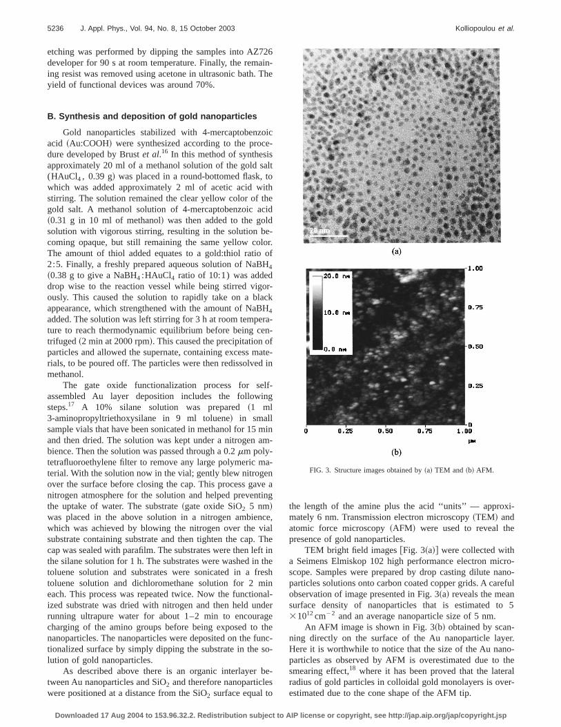
the length of the amine plus the acid ‘‘units’’ — approxmately 6 nm. Transmission electron microscopy~TEM! andatomic force microscopy~AFM! were used to reveal thepresence of gold nanoparticles.
TEM bright field images@Fig. 3~a!# were collected witha Seimens Elmiskop 102 high performance electron micscope. Samples were prepared by drop casting dilute nparticles solutions onto carbon coated copper grids. A carobservation of image presented in Fig. 3~a! reveals the meansurface density of nanoparticles that is estimated to31012cm22 and an average nanoparticle size of 5 nm.
An AFM image is shown in Fig. 3~b! obtained by scan-ning directly on the surface of the Au nanoparticle layHere it is worthwhile to notice that the size of the Au nanparticles as observed by AFM is overestimated due tosmearing effect,18 where it has been proved that the lateradius of gold particles in colloidal gold monolayers is oveestimated due to the cone shape of the AFM tip.
FIG. 3. Structure images obtained by~a! TEM and ~b! AFM.
license or copyright, see http://jap.aip.org/jap/copyright.jsp

eto
icti
r-
arao
a
p
t ibyE89
ing
ISsghithiteedexana-he
verayerasythem-top
that
-rV
sm
rs
ps.rgelm
toer-
ade
ne
cid
in-meForher-
sh
wsueep
5237J. Appl. Phys., Vol. 94, No. 8, 15 October 2003 Kolliopoulou et al.
III. ELECTRICAL CHARACTERIZATION ANDDEMONSTRATION OF MEMORY EFFECT
In Fig. 4, the transfer (I DS2VGS) characteristics in thelinear region (VDS5100 mV) are compared for the thretypes of FET device. For comparison all tested transishave a gate widthW510mm and a gate lengthL51.5mm. Thus, no short channel effects affect our devoperation and the memory characteristics are easily disguished. Threshold voltage (Vth) calculations have been peformed by adopting the constant current method:I DS(Vth)510 nA (W/L).19 It is evident from Fig. 4 that there isthreshold voltage variation as the insulator stack configution is changed, which is mainly attributed to the presencefixed charges in the organic insulator. This has been alreobserved in other LB deposited insulators and explainedtrapped charge at the interface between sequentially deited layers.20 Point defects observed by other researchersLB deposited cadmium arachidate films could also resulfixed charges.21 The subthreshold slope is also affectedthe nature of the insulating layer. The reference MOSFtransistor~device A! has a subthreshold slope equal tomV/dec, typical for long-channel devices,22 while that for theLB metal–insulator–semiconductor FET~MISFET! ~deviceB! is 523 mV/dec and that for the nanoparticle-containMISFET ~device C! is 364 mV/dec.
No hysteresis was noted in the current–voltage (I 2V)characteristics of either reference device~A or B! when thegate voltage sweep changed direction. However, the MFETs containing the Au nanoparticles possessed trancharacteristics with a hysteresis that increased as thevoltage increased. Typical behavior is shown in Fig. 5. Thysteresis is a well-known effect of charge storage ininsulator. Since neither of the reference devices exhibthis effect, we attribute the charge storage to the presencthe Au nanoparticles. It is significant that this hysteresisrection is counterclockwise, indicating that electrons aretracted from the nanoparticles for positive gate voltagesinjected into them from the gate electrode for negative gvoltages. Although the SiO2 layer used in this work is relatively thin ~5 nm!, the distance between the surface of t
FIG. 4. TransferI 2V characteristics of tested devices and their subthreold regions:~solid line! reference of 5 nm SiO2 MOSFET, ~dashed line!reference of 5 nm SiO2 plus the organic insulator layer MISFET, and~dottedline! MISFET single memory cell with Au nanoparticles. The inset shothe same curves in linear scale.
Downloaded 17 Aug 2004 to 153.96.32.2. Redistribution subject to AIP
rs
en-
-f
dyasos-inn
T
-feratesedof
i--d
te
silicon and the gold particles is effectively increased to o10 nm because of the presence of the amine capping lassociated with the Au nanoparticles. This prevents echarge transfer via tunneling from the semiconductor toAu. If we consider a simple tunnelling expression to copare the currents to the gold nanoparticles either from themetal gate electrode or from the Si channel we can write
I 5I 0exp~2kd~D!0.5!,
whereI 0 is a constant current value,k is a constant,d is theinsulator thickness, andD is the tunneling barrier of the insulator. For the Si/SiO2 system the energy barrier height foelectrons is 3.2 eV and for a fatty acid film values of 2 ehave been reported in the literature.23 Even if there is a low-ering of barrier height for the cadmium arachidate~Cd-AA!film its thickness cannot justify a direct tunneling mechanithrough it. However, it has been also reported24 that the dccurrent conductivity measured in LB deposited multilayecan be attributed to a combination of two mechanisms:~i!direct tunneling through each LB bilayer and~ii ! thermallyactivated hoping within the plane of carboxylic head grouThese mechanisms can satisfactorily explain the chatransfer to the gold nanoparticles through the fatty acid fiand not through the thermal oxide film.
In the following we fabricate simple MIS structuresget more experimental results of the dc conductivity propties of our insulators. In Fig. 6 we present results onJ2Vmeasurements of MIS structures where the insulator is mout of either a 5 nmthermal SiO2 @Fig. 6~a!#, or a deposited54 nm of the Cd-AA insulator on top of a native silicooxide layer@Fig. 6~b!#. The metal electrode is aluminum. Thsecond of these experiments@Fig. 6~b!# can be comparedwith previous measurements on the conductivity of fatty amultilayers performed either up to 0.8 V25 or up to 3 V. Wefind a good agreement of our measurements with thesevestigators. The current remains low in the sub-1 V regiand increases 2 orders of magnitude for voltages of 3 V.higher voltages the Cd-AA film of 54 nm breaks down. Tthin thermal oxide of 5 nm exhibits better insulating propeties for these voltage values@Fig. 6~a!# that can justify the
-
FIG. 5. TransferI 2V characteristics of tested MISFET with embedded Ananoparticles into the gate insulator measured with different voltage swlimits: ~open circles! 62 V, ~solid line! 64 V.
license or copyright, see http://jap.aip.org/jap/copyright.jsp

omruanct
teha
epu
Vtin
fgin
b
h
e.
athre
ckargear-
tyed
e-ntionap-
inti-4
sedityits
n–rge
tech-an-
ug
on
ces
-
5238 J. Appl. Phys., Vol. 94, No. 8, 15 October 2003 Kolliopoulou et al.
charging of the nanoparticles in our memory structure frthe top gate electrode. We remark that in the memory stture the insulation of the nanoparticles from the silicon chnel is even better because of the presence of the amineping layer between the nanoparticles and the surface ofthermal oxide.
The application of different voltage pulses to the gaelectrode may be used to elucidate the programming beior of these MISFET memory devices. In Fig. 7~a!, the effectof a symmetrical pulse sequence on the threshold voltagshown. The erase process was obtained by a saturation16 V for 1 s while for the write process a pulse26 V wasused with the same time period. If a gate voltage of 0.5was used for reading the memory, it was possible to disguish between a written~‘‘1’’ ! and the erased state~‘‘0’’ ! bythe drain current level. Figure 7~b! shows the dependence othreshold voltage shift on the height of the applied voltapulse. No change in the memory state was achieved utilizpulses well below 1 s.
The trapped charge density in the nanoparticles canestimated from the voltage shiftDVth @Fig. 7~b!# in our de-vice after a 6 V applied voltage pulse to the gate. From tvalue one comes to the trapped charge densityQ using Q5(DVth3C0), where C0 is the accumulation capacitancMeasurements giveC0 at 531028 F/cm2 from which Q iscalculated at 331027 C/cm2. The capacitance per unit areC0 was measured using a MIS capacitor structure with aoxide, amine layer, and the Cd-AA film since direct measu
FIG. 6. Current density as a function of the gate voltage flowing throthree different gate insulators of MIS capacitors:~a! 5 nm thermal SiO2 and~b! 54 nm of LB deposited Cd-AA insulator deposited on a native silicoxide layer.
Downloaded 17 Aug 2004 to 153.96.32.2. Redistribution subject to AIP
c--
ap-he
v-
islse
-
eg
e
is
in-
ments from transistor structures were difficult due to the laof substrate contact. To transfer the above estimated chfrom the gate through the organic insulator to the nanopticles in 1 s~programming time! one needs a current densiof 0.1mm/cm2 that is easily obtained as can be observfrom theJ2V measurement curve shown in Fig. 6~b!.
In order to check the nonvolatility of these memory dvices charge retention measurements of the charge retetime at room temperature have been performed throughplication of66 V gate voltage stress for 1 s with a source todrain bias at 0.1 V. The retention characteristics shownFig. 8 demonstrate that the memory window is not praccally decreased from its initial value for times as long as3104 s. This reveals a remarkable potential for the propodevice as a nonvolatile memory given not only the simplicof its fabrication technology but also the early stage ofdevelopment.
IV. CONCLUSIONS
In summary, we have demonstrated a hybrid silicoorganic memory device using gold nanoparticles as chastorage elements deposited by a chemical self-assemblynique. The nanoparticles are separated from the silicon ch
h
FIG. 7. Programming characteristics of MISFETs single memory deviwith Au nanoparticles embedded into the gate insulator stack:~a! write/erase(W/E) process obtained by applying26 and 6 V voltage pulses, respectively. The pulse period was 1 s.~b! The effect of the programming voltageon the memory window for pulse 1 s.
license or copyright, see http://jap.aip.org/jap/copyright.jsp

ea
orteimheodlrtht.
C
s, S.
an,
ron
R.
ac.
ett.
pl.
G.
c.,
uir
n
r.
5239J. Appl. Phys., Vol. 94, No. 8, 15 October 2003 Kolliopoulou et al.
nel by a 5 nmthermal SiO2 layer and from the gate electrodby an organic insulator deposited by the LB techniqueroom temperature. The device exhibits nonvolatile memcharacteristics at low operation voltages, is batch fabricaand does not show any change of its characteristics with tin normal ambient conditions. For efficient fabrication of tdevice, two very different processing technologies, silictechnology and organic thin film deposition had to be aequately integrated. This technology has also the potentiabe explored for application in organic memory devices. Moinvestigations are in progress to understand furthercharge transfer process that generates the memory effec
ACKNOWLEDGMENT
The authors acknowledge financial support from Ethrough the FET-IST project FRACTURE~Contract No.26014!.
FIG. 8. Retention characteristics of sample C after application of66 V onthe gate for 1 s.
Downloaded 17 Aug 2004 to 153.96.32.2. Redistribution subject to AIP
tyd,e
n-toee
1H. I. Hanafi. S. Tiwari, and I. Khan, IEEE Trans. Electron Devices43,1553 ~1996!.
2E. Kapetanakis, P. Normand, D. Tsoukalas, K. Beltsios, J. StoemenoZhang, and J. van den Berg, Appl. Phys. Lett.77, 3450~2000!.
3M. Ostraat, J. De Blauwe, M. Green, D. Bell, H. Atwater, and R. FlagJ. Electrochem. Soc.148, G265~2001!.
4Y.-C. King, T.-J. King, and C. Hu, IEEE Trans. Electron Devices48, 696~2001!.
5Z. Liu, C. Lee, V. Narayanan, G. Pei, and E.-C. Kan, IEEE Trans. ElectDevices49, 1614~2002!.
6J. Liu, T. Lee, D. B. Janes, B. L. Walsh, M. R. Melloch, J. M. Woodall,Reifenberger, and R. P. Andres, Appl. Phys. Lett.77, 373 ~2000!.
7T. Sato and H. Ahmed, Appl. Phys. Lett.70, 2759~1997!.8J. Yang, L. de la Garza, T. J. Thornton, M. Kozicki, and D. Gust, J. VSci. Technol. B20, 1706~2002!.
9Y. Cui, Q. Wei, H. Park, and C. M. Lieber, Science293, 1289~2001!.10J. Collet, O. Tharaud, A. Chapoton, and D. Vuillamme, Appl. Phys. L
76, 1941~2000!.11J. Collet, and D. Vuillamme, Appl. Phys. Lett.73, 2681~1998!.12H. E. Katz, X. M. Hong, A. Dodabalapur, and R. Sarpeshkar, J. Ap
Phys.91, 1572~2002!.13L. P. Ma, J. Liri, and Y. Yang, Appl. Phys. Lett.80, 2997~2002!.14G. Velu, C. Legrand, O. Tharaud, A. Chapoton, D. Remiens, and
Horowitz, Appl. Phys. Lett.79, 659 ~2001!.15C. P. Ho and J. D. Plummer, J. Electrochem. Soc.126, 1523~1979!.16M. Brust, J. Fink, D. Bethell, D. J. Schiffrin, and C. Kelly, J. Chem. So
Chem. Commun.16, 1655~1995!.17S. R. Johnson, S. D. Evans, and R. Brydson, Langmuir14, 6638~1998!.18J. Schmitt, P. Machtle, D. Eck, H. Mohwald, and C. A. Helm, Langm
15, 3256~1999!.19D. K. Schroder,Semiconductor Material and Device Characterizatio,
2nd ed.~Wiley, New York, 1998!, p. 247.20N. J. Evans, M. C. Petty, and G. G. Roberts, Thin Solid Films160, 177
~1988!.21G. Nechev, M. Hibino, and I. Hatta, Colloids Surf., A166, 1 ~2000!.22S. Wolf, Silicon Processing for the VLSI Era~Lattice, 1990!, Vol. 2, p.
311.23E. E. Polymeropoulos and J. Sagiv, J. Chem. Phys.69, 1836~1978!.24A. V. Nabok, B. Iwantono, A. K. Hassan, A. K. Ray, and T. Wilkop, Mate
Sci. Eng., C22, 355 ~2002!.25B. Mann and H. Kuhn, J. Appl. Phys.42, 4398~1971!.
license or copyright, see http://jap.aip.org/jap/copyright.jsp