Growth of Indium Oxide and Zinc‐Doped Indium Oxide Nanostructures
Upload
independentCategory
view
5download
0
Published: January 5, 2011
r 2011 American Chemical Society 1415 dx.doi.org/10.1021/jp1069237 | J. Phys. Chem. C 2011, 115, 1415–1421
ARTICLE
pubs.acs.org/JPCC
Structure and Photoluminescence of Pure and Indium-Doped ZnTeMicrostructuresWeichang Zhou,†,‡ Dongsheng Tang,† Anlian Pan,‡ Qinglin Zhang,‡ Qiang Wan,‡ and Bingsuo Zou*,§,‡
†Key Laboratory of Low-Dimensional Quantum Structures and Quantum Control of Ministry of Education, College of Physics andInformation Science, Hunan Normal University, Changsha 410081, People's Republic of China‡School of Physics and Microelectronics Science, Hunan University, Changsha 410082, People's Republic of China§School of Material Science and Engineering, Beijing Institute of Technology, Beijing 100081, People's Republic of China
ABSTRACT: High-purityand doped ZnTe micro-structures were synthe-sized with a single thermalevaporation method. Themorphology of doped ZnTemicrostructures showsmulti-layered periodical structure,which is due to the incor-poration of In elements. ThePL investigation demons-trated that the pure ZnTemicrostructures emit onlygreen light (close to thebandedge) while ZnTe doped with varied In concentrations emit red or infrared light without band-edge emission. These emissionchanges reflected that the Donor-Acceptor pair state transition can be tuned in semiconductor microstructures for futureapplications.
1. INTRODUCTION
One-dimensional (1-D) semiconductor nanostructures haveattracted much attention due to their unique electronic, optical,and optoelectronic properties and their potential novel applica-tions in nanodevices.1-4 Among these nanometer-scale semi-conductor materials, II-VI semiconductor nanostructures havebeen investigated widely and demonstrated potential applicationin lasers,5 optical waveguides,6 photodetectors,7 and field effecttransistors.8 Zinc telluride (ZnTe), as a direct semiconductorwith a band gap of 2.28 eV (∼545 nm) at room temperature, is animportant member of the II-VI family and an attractive materialfor various optoelectronic devices, such as green LEDs andphotovoltaic cells.9,10 There are many reports on the photo-luminescence of ZnTe thin film or bulk material.11,12 To date, therewere only some works available on the preparation and opto-electronic properties of 1-D ZnTe nanostructures.13-16 The lowand room temperature PL spectra of single crystalline ZnTenanowires, synthesized via the vapor phase transport method,showed near band-edge emission.16 According to the energyband theory, the emission wavelength and hence the emittedcolor is based on high-purity quality and band-edge emission.The bandgaps of its binary or typically unintentionally dopedsemiconductor nanostructures can hardly be tuned for theirdefinite components, which restricts their further application indifferent fields. This situation can be improved by doping semi-
conductor nanostructures, which maymodulate the band gaps orproduce deeptrap, thus emitting light of varied wavelengths,which sometimes simultaneously changes its phase structure.17
For example, Peng et. al18 showed that doped ZnSe nanocrystalswith different dopant concentrations can emit tunable color lightwhile still holding matrix ZnSe crystal phase structures. There-fore, intentional doping can greatly modify the electronic statesand therein emissions of II-VI semiconductor nanostructures.
To the best of our knowledge, there are no reports so far aboutthe synthesis of In doped ZnTe microstructures and their effecton the PL properties of ZnTe. In the present work, we focus onthe incorporation of Indium into ZnTe microstructures andstudy their PLs. Indium is selected as the dopant because it isrecognized as one of the most efficient elements used to improvethe opto-electrical properties of compounds.19 For comparison,we also synthesized pure ZnTe microstructures. The pure ZnTemicrostructures show a green emission, whereas doped ZnTemicrostructures show a red or infrared emission for their differentdopant concentrations. Our results indicated a modulated PLemission from green to red or infrared due to the intentionaldoping with different dopant concentrations. Such novel red or
Received: July 25, 2010Revised: November 24, 2010
1416 dx.doi.org/10.1021/jp1069237 |J. Phys. Chem. C 2011, 115, 1415–1421
The Journal of Physical Chemistry C ARTICLE
infrared light emissions are expected to have potential applica-tions in various micro/nano-optoelectronic devices in the visibleor infrared range.
2. EXPERIMENTAL METHODS
The ZnTe and In-ZnTemicrostructures were synthesized by aphysical evaporation method. Appropriate amounts of commer-cial grade ZnTe powder were placed onto a ceramic boat at thecenter of a quartz tube, which was placed into a horizontal tubefurnace. Next to the ceramic boat, several pieces of silicon slicescoated with 5 nm Au film were placed downstream of the gasflow. High-purity Ar(95%)/H2(5%) was injected into the quartztube with a constant flow rate (100 SCCM) to eliminate the O2
inside before heating. The flow rate of Ar/H2 gas was adjusted to10 SCCM after 90 min and the furnace was rapidly heated to1000 �C and maintained for about 60 min without changing anyconditions. When the furnace cooled down, pale red products aredeposited onto the surfaces of the silicon slices in the tempera-ture range of 450-550 �C. For In doped ZnTe microstructures,we used mixed Indium powder and the above ZnTe powder asthe source materials. In our present typical synthesis, the mixedpowder of ZnTe and In of 10:1 and 5:1 weight ratios, respec-tively, are used as source materials, and their related products aremarked as samples A and B, respectively. The doped ZnTemicrostructures were obtained at 1000 �C for about 30 min, withblack products deposited on the surface of the Si substrates.
After the synthesis, FE-SEM (JSM-6700F), XRD (using aD/max 5000 utilizing CuKa radiation), and TEM (JEM-3010)were used to examine the morphology and phase structures ofas-prepared microstructures. The Photoluminescence (PL) andRaman spectra were obtained by Scanning Near-field OpticalMicroscopy (SNOM, alpha 300 series, WITec GmbH, UlmGermany) using an Arþ laser with a wavelength of 488 nm asthe excitation source at room temperature.
3. RESULTS AND DISCUSSION
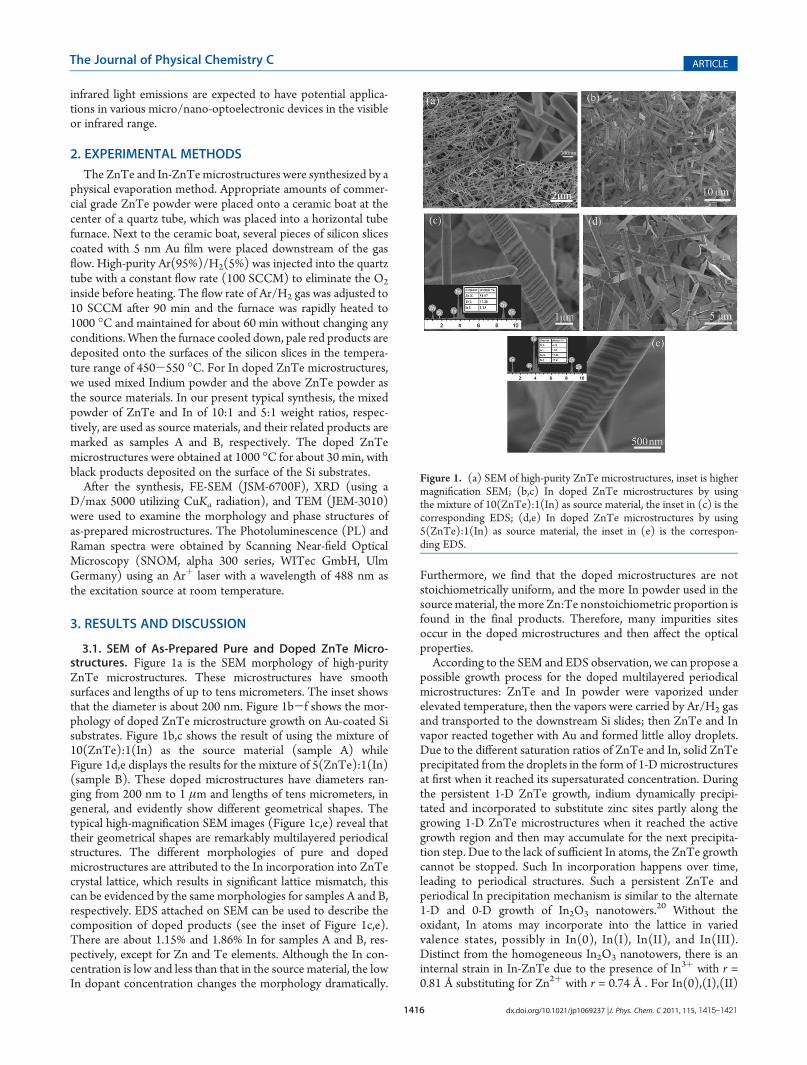
3.1. SEM of As-Prepared Pure and Doped ZnTe Micro-structures. Figure 1a is the SEM morphology of high-purityZnTe microstructures. These microstructures have smoothsurfaces and lengths of up to tens micrometers. The inset showsthat the diameter is about 200 nm. Figure 1b-f shows the mor-phology of doped ZnTe microstructure growth on Au-coated Sisubstrates. Figure 1b,c shows the result of using the mixture of10(ZnTe):1(In) as the source material (sample A) whileFigure 1d,e displays the results for the mixture of 5(ZnTe):1(In)(sample B). These doped microstructures have diameters ran-ging from 200 nm to 1 μm and lengths of tens micrometers, ingeneral, and evidently show different geometrical shapes. Thetypical high-magnification SEM images (Figure 1c,e) reveal thattheir geometrical shapes are remarkably multilayered periodicalstructures. The different morphologies of pure and dopedmicrostructures are attributed to the In incorporation into ZnTecrystal lattice, which results in significant lattice mismatch, thiscan be evidenced by the samemorphologies for samples A and B,respectively. EDS attached on SEM can be used to describe thecomposition of doped products (see the inset of Figure 1c,e).There are about 1.15% and 1.86% In for samples A and B, res-pectively, except for Zn and Te elements. Although the In con-centration is low and less than that in the source material, the lowIn dopant concentration changes the morphology dramatically.
Furthermore, we find that the doped microstructures are notstoichiometrically uniform, and the more In powder used in thesourcematerial, the more Zn:Te nonstoichiometric proportion isfound in the final products. Therefore, many impurities sitesoccur in the doped microstructures and then affect the opticalproperties.According to the SEM and EDS observation, we can propose a
possible growth process for the doped multilayered periodicalmicrostructures: ZnTe and In powder were vaporized underelevated temperature, then the vapors were carried by Ar/H2 gasand transported to the downstream Si slides; then ZnTe and Invapor reacted together with Au and formed little alloy droplets.Due to the different saturation ratios of ZnTe and In, solid ZnTeprecipitated from the droplets in the form of 1-Dmicrostructuresat first when it reached its supersaturated concentration. Duringthe persistent 1-D ZnTe growth, indium dynamically precipi-tated and incorporated to substitute zinc sites partly along thegrowing 1-D ZnTe microstructures when it reached the activegrowth region and then may accumulate for the next precipita-tion step. Due to the lack of sufficient In atoms, the ZnTe growthcannot be stopped. Such In incorporation happens over time,leading to periodical structures. Such a persistent ZnTe andperiodical In precipitation mechanism is similar to the alternate1-D and 0-D growth of In2O3 nanotowers.20 Without theoxidant, In atoms may incorporate into the lattice in variedvalence states, possibly in In(0), In(I), In(II), and In(III).Distinct from the homogeneous In2O3 nanotowers, there is aninternal strain in In-ZnTe due to the presence of In3þ with r =0.81 Å substituting for Zn2þ with r = 0.74 Å . For In(0),(I),(II)
Figure 1. (a) SEM of high-purity ZnTe microstructures, inset is highermagnification SEM; (b,c) In doped ZnTe microstructures by usingthe mixture of 10(ZnTe):1(In) as source material, the inset in (c) is thecorresponding EDS; (d,e) In doped ZnTe microstructures by using5(ZnTe):1(In) as source material, the inset in (e) is the correspon-ding EDS.

1417 dx.doi.org/10.1021/jp1069237 |J. Phys. Chem. C 2011, 115, 1415–1421
The Journal of Physical Chemistry C ARTICLE
with larger radii than that of In(III), the strain should be evenlarger. This large difference of ionic radius between Zn2þ and Inresulted in dramatic structural fluctuation, hence leading to aclear intermediate growth rate variation for ZnTe crystal growth,and a multilayered periodical structure under discontinuousfeeding of evaporation gas due to In gas intervenes. Summarily,the alternating precipitation of indium accompanied with persis-tent precipitation of ZnTe is key to changing the diameter andultimately results in the diameter-modulated feature in someregions in the present 1-D doped microstructures.3.2. XRD of As-Prepared Pure and Doped ZnTe Micro-
structures. The structures of as-grown pure and doped ZnTemicrostructures are determined by XRD (see Figure 2). All of theXRD diffraction peaks of pure ZnTe can be assigned to the cubicZnTe structure with lattice constants of a = 6.1026 Å, consistentwith the standard data. With the exception of the standard ZnTediffraction peaks, there are some diffraction patterns fromTe andIn3Te4 in the doped ZnTe microstructures. This result indicatesthat the doping growth process is complex and In has multivalentstates in the doped structure, even to In(III), some Zn may flyaway during growth and Te separate out due to the thermaldecomposition. Some ZnTe gas may be reduced to Te(g) byheating. Te(g) can oxidize the In atoms to different valence statesfor the next incorporation step. Because the oxidation power ofTe(g) is not strong, some Te may be left and deposited withelemental state. When Indium doped into ZnTe crystal, In atomsor ions may substitute for some zinc to form a minor In3Te4compound within ZnTe. Some elemental Te may detachfrom the ZnTe crystal and deposit onto the surface of theAu-coated silicon substrate. According to the EDS of a singlemicrostructure (see the inset of Figure1c,e), we find that thecontent of Te is less than that of Zn, which suggests that some Tedoes detach from the ZnTe crystal when the Zn go out. More-over, according to HRTEM (see Figure 3d), we can see that thesingle microstructure is a single-phase structure. Therefore, thedetached Te deposits separately on the Si substrate and does notattach onto the doped microstructures. These diffraction peaksof impurity suggest that there may be various local defects, suchas impurities, vacancies, or dislocations, in the doped micro-structures. Furthermore, the diffraction intensity of impurity isweaker than that of ZnTe, which indicates a low content of In, as
EDS indicates. The strongest diffraction peak is [111] in threeXRDs andmay suggest the [111] direction as the primary growthdirection in these 1-D microstructures, and that the dopant doesnot change the growth direction of ZnTe. In fact, this argument isnot determined. The [111] growth direction is well accepted tobe the most densely packed surface for fcc structure in nano-structure growth. We will further discuss their growth directionsaccording to the HRTEM observations.3.3. TEM and HRTEM of Pure and Doped ZnTe Micro-
structures. The phase, growth orientation, characteristics ofcrystal lattice, and so forth of pure and doped ZnTe microstruc-tures were further characterized with TEM and high resolutionTEM (HRTEM). Figure 3a is the low magnification TEM ofpure ZnTe microstructures with diameters of 300 nm. Thesurface of pure ZnTe microstructure is very smooth, which isconsistent with the SEM result. But its surface contains someamorphous layers, which may influence its optical properties.The reason for this phenomenon is also related to the Tedetachment. Figure 3b shows its HRTEM. The HRTEM latticeimage confirms the single-crystalline structure of as-preparedmicrostructures. Furthermore, the measured lattice stripe spa-cing in HRTEM is 0.35 nm, corresponding to the interplanardistance of (111) planes as known from bulk cubic ZnTe crystal.Therefore, the growth orientation of pure ZnTe microstructuresis assigned to be [111].We also carried out the TEM and HRTEM measurements of
doped ZnTe microstructures (1.15% In). Figure 3c is the typicalTEM image of the doped microstructure. Different from thesmooth surface of pure microstructures, the doped microstruc-ture surface shows periodical paired zigzags along the long axis.Figure 3d corresponds to the HRTEM image. A diameter-modulated feature is clearly observed. Such HRTEM imagesalso show single-crystalline structure. The measured lattice stripespacing in HRTEM is also 0.35 nm, which corresponds to the
Figure 2. Normalized XRDs of pure ZnTe and doped ZnTe micro-structures with different dopant concentration, respectively. The stron-gest diffraction peak of sample B comes from the silicon wafer substrate.
Figure 3. (a) TEM of high-purity ZnTe microstructures; (b) HRTEMof high-purity ZnTe microstructure; (c) TEM of doped ZnTe micro-structures (1.15% In); and (d) HRTEM of doped ZnTe microstructure(1.15% In).

1418 dx.doi.org/10.1021/jp1069237 |J. Phys. Chem. C 2011, 115, 1415–1421
The Journal of Physical Chemistry C ARTICLE
interplanar distance of (111) planes of doped ZnTe crystal. (Thevariation of lattice stripe spacing due to the low doped concen-tration of In is small and within the measurement error.) In thisHRTEM image, we also find another orientation region(withinlabeled cycle zone) with an angle of 60� to the [111] stripe lines,which should be that modified by In doping. Therefore, thegrowth orientation of doped ZnTe microstructures can also beassigned to [111]. The minor In doping just changes the localstructure periodically, which leads to a slight modification ofgrowth direction, but does not change the growth direction in thedoped microstructures. Since XRD patterns are mainly deter-mined by their selection rules, we cannot assign this patternprofile to the orientation of [111] through examination, althoughsome reports indicate that this argument is possible.21,22
3.4. PL Characterization of Pure ZnTe Microstructures atRoom Temperature. As is well-known, photoluminescence(PL) is a sensitive noncontact and nondestructive techniquefor the measurement of the band structure and trapped states insemiconductors and can be used to characterize defect states,such as substitutional impurities (donors and acceptors) andnative or intrinsic defects in semiconductors. Figure 4a is the PLcharacterization of high-purity ZnTe microstructures. The insetin Figure 4a is the far dark-field optical image of the ZnTemicrostructure under excitation of Arþ laser (488 nm). We canobserve by the naked eye that the green light emission of ZnTe(see the bright facula in the lower inset of Figure 4a) under lowlaser excitation power. The emission intensity increases andthe emission band becomes broader at higher excitation power,and the emission color gradually changes from green to yellow,or even white. This variation can be verified by the correspon-ding PL spectra under different excitation powers. At lowexcitation power, the emission band is located at 548 nm, whichis related to the bandedge emission of ZnTe (2.28 eV) at roomtemperature.23
The PL of semiconductor nanowire or microwire usuallyoriginates from the radiative recombination of exciton or photo-indueced carriers, both local and/or delocalized. The magnitudeof exciton binding energy is critical to the stability of exciton atthe circumstance temperature. As the exciton binding energy12.9 meV is lower than the kinetic energy (26 meV) at roomtemperature, so the free exciton cannot be present due to thermal
dissociation, hence the delocalized carriers near the band-edgecan be dominant with significant phonon scattering. The datafrom Landolt-B€ornstein III/44B24 indicate that the free excitonbinding energy of ZnTe is in the range of 11-17 meV, and manyshallow doping impurities have binding energies of less than7 meV. These binding energy values in ZnTe cannot overrun thethermal dissociation force to avoid dissociation, while pure ZnOcrystal can keep exciton and show exciton emission at roomtemperature. Therefore, the emission near the band-edge of pureZnTe is from the radiation transition between delocalizedcarriers, which is broad due to the phonon and surface scatteringin 1-d carrier transport.25
With rising excitation power, emission intensity increases formore carriers were produced, at the same time the emissionbands redshift from 548 to 582 nm and become broader. It iswell-known that the emission usually occurs near the band-edgein bulk direct semiconductors at room temperature, for mostII-VI semiconductors have exciton binding energies less than orcomparable to kT(26 meV) at room temperature, with theexception of ZnO. So the photonexcited carriers are the originof radiative recombination. More carriers at higher excitationundergo strong coulombic repulsion forces due to the band-filling effect.25,26 The population of newly produced carriers goesto a lower energy, which behaves in such a way that the apparentband-edge shrinks to a lower energy, therefore the opticaltransitions do the same. All of the shifts under varied excitationpower can be assigned to exciton-carrier and exciton-phononinteractions near the dynamic band-edge. The surface amor-phous layer, indicated by the HRTEM characterization(Figure 3), can enhance the exciton dissociation and the surfacescattering even in CdS nanowires.25 Hence the more carriers areproduced, the more redshift due to the bandgap renormalizationand plasma effect occurs.26 This character reflects the low excitonstability and possible relaxation due to surface structural imper-fections. Figure 4b shows that the emission intensity increasesrapidly with excitation power and then gradually saturates underhigh excitation power, reflecting the typical features of electron-hole plasma in semiconductors. For the lD transport, we did notsee the intensity decrease due to saturation, but rather a slowincrease instead.
Figure 4. (a) The PL of pure ZnTe microstructures under different excitation power at room temperature; Insets are the far dark-field emission imagesunder high and low excitation power, respectively. (b) Intensity and fwhm variation of bandgap or near- bandgap emission under different excitation power.

1419 dx.doi.org/10.1021/jp1069237 |J. Phys. Chem. C 2011, 115, 1415–1421
The Journal of Physical Chemistry C ARTICLE
3.5. PL Characterization of Doped ZnTe Microstructureswith Different In Concentrations. For wide band gap semi-conductors, doping often induces dramatic changes in electricaland optical properties.26,27 We have observed their changes inmorphology (see Figure 1). Figure 5 is the PL spectra of dopedZnTe microstructures with 1.15% In concentration (sample A).The left-bottom inset in Figure 5 is the dark-field image underexcitation when the laser is focused on a selected area in a repre-sentative microstructure. The sample emits red light under exci-tation. The PL spectra show that the emission band maximumlocate principally at 713 nm with a multipeak profile (this spectracan be fitted with more minibands) while the band edge emission(548 nm) cannot be detected. Furthermore, the emission peaklocation and line shape show no change at rising excitationpowers. Since the energy of this emission peak shows no shiftwith excitation power, it is considered to be bound staterecombination at local donor-acceptor (possibly In(0)-In(III)or In(0)-Zn vacancy). There are two reasons for its assignment.(1) Its location is far from the bandedge, which is usually due tothe deeptrap emission.23,28 In this system, the deeptrap maycome from the In or Zn vacancy. The latter emission is often at580-600 nm, so In deeptrap is more possible. (2) In usual cases, ifthe emission is related to the itinerant carriers, then we find that itshiftswith greater carrier population.Herewe findno shift, so its localtransition nature is definite. Because of the multivalent (multilevels)state of the In dopant, the multilevel profile can be observed, as inFigure 5.Thismultilevel energy iswithin the bandgapofZnTe, so theIn dopant can be seen as a color center in the crystal.Most of the excited carriers under excitation are trapped (less
than 1 ps) by acceptor levels or defect centers in dopedsemiconductors, making the luminescence dominant throughthe trapped state recombination. In the present PL spectra, theorigin of red emission in doped ZnTe microstructures can beattributed to excitons bound to the doped indium levels becausesingle In(I) has an excess of electrons, which may lead to comp-licated emission profiles if an In(III) or a vacancy acceptor exist.Indium atoms usually acted as deep-lying donors and the formedindium donor level lies 0.4-0.6 eV beneath the conduction bandin sulfide;29,30 however, the DX state usually shifts with rising
excitation like excitons. According to our present PL results, wecan estimate the indium donor level located less than 0.4 eVbeneath the conduction band, which is also consistent with thevalue of 0.5 eV in In-ZnS phosphors.31 Furthermore, the fwhm(about 89 nm) in doped microstructures is larger than that ofpure ZnTe microstructures, which is also a consequence of astrong exciton coupling with the lattice, as well as the presence ofdefect complexes with slightly separated energy levels. In addi-tion, different from the band edge emission of pure ZnTemicrostructures, these emission peaks of doped ZnTe show noredshift under rising excitation power, which demonstrates theirlocal trapping nature in the microstructures. Due to the In(III)(acceptor center) existence, this transition may not be from a DXstate with delocalized nature, but a possible DA pair(DAP) withlocal transition. The In(I)-In(III) pair may be one possiblechannel for the band at 713 nm located at the high excitationpower. Such red emission in the doped ZnTe microstructuresmay work as that of CdSe5 or Se-CdS17 nanostructures andsubstitute for the heavy metals in them.Figure 6a shows the PL spectra of doped microstructures with
1.86% In concentration (sample B). We observe the emissionband maximum shift to 837 nm and we observe no shift under
Figure 5. The PL of doped ZnTe microstructures with 1.15% In underdifferent excitation power at room temperature; Upper inset is the fittedPL spectrum of a representative spectrum with Gaussian function;Lower inset is the far dark-field emission image under laser excitation.
Figure 6. (a) ThePL spectra of dopedZnTemicrostructureswith 1.86% Inunder different excitation power at room temperature. (b) The correspond-ing Raman spectrum with 488 nm (Arþ laser) as the excitation source.
1420 dx.doi.org/10.1021/jp1069237 |J. Phys. Chem. C 2011, 115, 1415–1421
The Journal of Physical Chemistry C ARTICLE
rising excitation power, while we cannot observe the band-edgeemission. Compared with the emission of sample A with 1.15%In, this PL shows infrared emission and the emission colorcannot be seen by the naked eye, which is consistent with theblack color of the sample. Similar to red emission, this infraredemission can be attributed to recombination between indiumdonor and deep-lying acceptors, such as Y band, which usuallyappear in wide bandgap semiconductors.32,33 The Y band isrelated to the lattice imperfection, structure defects, and disloca-tion, and locates at about 170-270 meV above the valenceband.34-36 Here the In(III) may be the dominant acceptor. Theoptical characteristics of the Y band strongly depend on theimpurity density and growth conditions. Our doping process notonly produced the diffusion of In, but also introduced the highdensity of defect states, such as: Zn vacancy (Vzn) or aggregatedIn pairs. Therefore, the intensity of trapping states is higher whenmore In is doped into the ZnTe crystal. Careful observationshows that the infrared emissions at above 800 nm also exist insample A, which can be divided intomore emission bands, see theupper inset in Figure 5. These results reflected multi-DA pairs inthis doping sample, like the In(0)-In(III) pair, because theradiative charge transfer transition between D and A determinesthe location of the emission wavelength. When the In concen-tration increase, more In(0) and In pairs populate, so theIn(0)-In(III) pair may be dominant over the In(I)-In(III)pair, therefore producing the emission at 837 nm. The color ofthe sample becomes dark black, which also proves this tendency.Moreover, the In(0) has two electrons ready to be released, itsemission (Figure 6) should be stronger than that (Figure 5) ofIn(I) at the start. Therefore, the donor-acceptor (Y band)complex emission under higher dopant concentration reflectedan In valence state modulation in the ZnTe doping microstruc-tures, producing a redshift emission.Multiphonon often occurs in the local exciton excitation
case.37 Figure 6b is the Raman spectrum of sample B, whichwas obtained by using 488 nm as the excitation source. Severalsharp vibration modes in the Raman spectrum are detected,which are at 479, 715, 951, 1187, 1423 cm-1 and correspondingshoulder peaks locate at 533, 769, 1005, 1241, 1477 cm-1,respectively. Irwin et. al investigated the Raman scattering ofZnTe systematically and listed many vibration modes of ZnTecrystal, such as LO(Γ)-208 cm-1, TO(Γ)-178 cm-1, LO(X)-182cm-1, TO(X)-173 cm-1, LA(X)-143 cm-1, TA(X)-54 cm-1,LO(L)-172 cm-1, TO(L)-171 cm-1, LA(L)-154 cm-1, TA(L)-46 cm-1, 228 cm-1-TO(X)þTA(X), 240cm-1-LO(X)þTA(X).38
In our present results, the differences between neighboringsharp vibration modes are uniform at 236 cm-1, which isconsistent with the TA(X)þTO(X) mode. The differencebetween sharp vibration modes and their correspondingshoulder peaks is 54 cm-1, which equals TA(X). We also doRaman scattering measurement in sample A, but cannot observeany Raman peaks due to its strong emission. This is becauseits emission band is close to the Raman scattering peaks. Theweak acoustic phononmode observed in our doped ZnTemicro-structures comes from the doping effect and the resultingselection rule relaxation. Local vibration enhancement alwaysaccompanies the acoustic modes and multiphonon scattering indoped nanostructures or layer-like structures.39,40 Therefore,the acoustic mode and the optical mode combine and appeartogether in the microstructures, verifying that the impurity iondoped into the ZnTe crystal and therein induced multilayeredperiodical structures. We also see that the phonon overtone
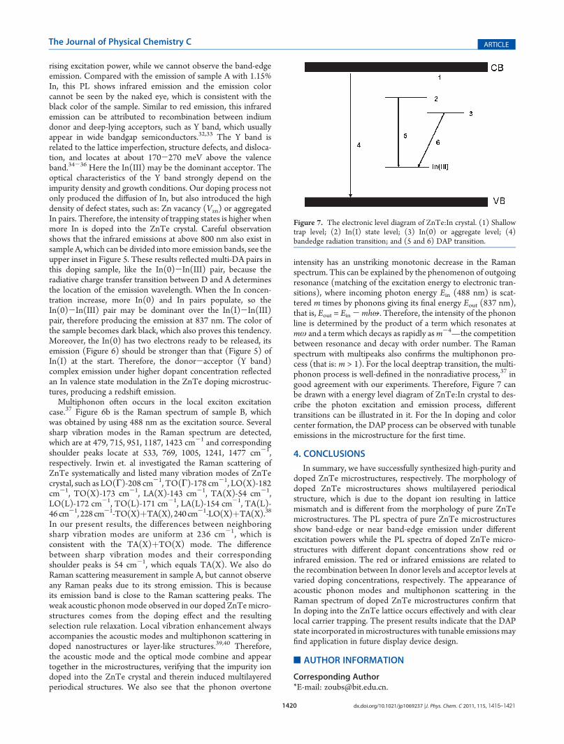
intensity has an unstriking monotonic decrease in the Ramanspectrum. This can be explained by the phenomenon of outgoingresonance (matching of the excitation energy to electronic tran-sitions), where incoming photon energy Ein (488 nm) is scat-tered m times by phonons giving its final energy Eout (837 nm),that is, Eout = Ein-mhω9. Therefore, the intensity of the phononline is determined by the product of a term which resonates atmω and a term which decays as rapidly asm-4—the competitionbetween resonance and decay with order number. The Ramanspectrum with multipeaks also confirms the multiphonon pro-cess (that is: m > 1). For the local deeptrap transition, the multi-phonon process is well-defined in the nonradiative process,37 ingood agreement with our experiments. Therefore, Figure 7 canbe drawn with a energy level diagram of ZnTe:In crystal to des-cribe the photon excitation and emission process, differenttransitions can be illustrated in it. For the In doping and colorcenter formation, the DAP process can be observed with tunableemissions in the microstructure for the first time.
4. CONCLUSIONS
In summary, we have successfully synthesized high-purity anddoped ZnTe microstructures, respectively. The morphology ofdoped ZnTe microstructures shows multilayered periodicalstructure, which is due to the dopant ion resulting in latticemismatch and is different from the morphology of pure ZnTemicrostructures. The PL spectra of pure ZnTe microstructuresshow band-edge or near band-edge emission under differentexcitation powers while the PL spectra of doped ZnTe micro-structures with different dopant concentrations show red orinfrared emission. The red or infrared emissions are related tothe recombination between In donor levels and acceptor levels atvaried doping concentrations, respectively. The appearance ofacoustic phonon modes and multiphonon scattering in theRaman spectrum of doped ZnTe microstructures confirm thatIn doping into the ZnTe lattice occurs effectively and with clearlocal carrier trapping. The present results indicate that the DAPstate incorporated inmicrostructures with tunable emissionsmayfind application in future display device design.
’AUTHOR INFORMATION
Corresponding Author*E-mail: [email protected].
Figure 7. The electronic level diagram of ZnTe:In crystal. (1) Shallowtrap level; (2) In(I) state level; (3) In(0) or aggregate level; (4)bandedge radiation transition; and (5 and 6) DAP transition.

1421 dx.doi.org/10.1021/jp1069237 |J. Phys. Chem. C 2011, 115, 1415–1421
The Journal of Physical Chemistry C ARTICLE
’ACKNOWLEDGMENT
We thank the NSF of China (Term Nos. 90606001, 20873039,90406024, 90923014, and 10974050), Hunan Provincial NaturalScience Foundation (07JJ4002 and 09JJ1009), New Century Excel-lent Talents in University (NCET-08-0182), and Science and Tech-nology InnovativeResearchTeam inHigherEducational Instituions ofHunan Province for financial support.
’REFERENCES
(1) Wang, Z. L.; Nanowires and Nanobelts, Vol. II: Nanowires andNanobelts of Functional Materials; Kluwer Academic: New York, 2006.(2) Xia, Y. N.; Yang, P. D.; Sun, Y. G.; Wu, Y. Y.; Mayers, B.; Gates,
B.; Yin, Y. D.; Kim, F.; Yan, H. Q. Adv. Mater. 2003, 15, 353.(3) Li, Y.; Qian, F.; Xiang, J.; Lieber, C. M.Mater. Today 2006, 9, 18.(4) Thelander, C.; Agarwal, P.; Brongersma, S.; Eymery, J.; L. Feiner,
F.; Forchel, A.; Scheffler, M.; Riess, W.; Ohlsson, B. J.; G€osele, U.;Samuelson, L. Mater. Today 2006, 9, 28.(5) Pan, A. L.; Liu, R. B.; Zhang, Q. L.; Wan, Q.; He, P. B.; Zacharias,
M.; Zou, B. S. J. Phys. Chem. C 2007, 111, 14253.(6) Pan, A. L.; Liu, D.; Liu, R. B.; Wang, F. F.; Zhu, X.; Zou, B. S.
Small 2005, 1, 980.(7) Singh, A.; Li, X. Y.; Protasenko, V.; Galantai, G.; Kuno, M.; Xing,
H. L.; Jena, D. Nano Lett. 2007, 7, 2999.(8) Wang, Y. G.; Zou, B. S.; Wang, T. H.; Wang, N.; Cai, Y.; Chan,
Y. F.; Zhou, S. X. Nanotechnology 2006, 17, 2420.(9) Tanaka, T.; Matsuno, Y. J.; Kume, Y.; Nishio, M.; Guo, Q. X.;
Ogawa, H. Phys. Status Solidi B 2004, 1, 1026.(10) Bozzini, B.; Baker, M. A.; Cavallotti, P. L.; Cerri, E.; Lenardi, C.
Thin Solid Films 2000, 388, 361.(11) Sato, K.; Adachi, S. J. Appl. Phys. 1993, 73, 926.(12) Chang, J. H.; Cho, M. W.; Wang, H. M.; Wenisch, H.; Hanada,
T.; Yao, T.; Sato, K.; Oda, O. Appl. Phys. Lett. 2000, 77, 1256.(13) Li, L.; Yang, Y. W.; Huang, X. H.; Li, G. H.; Zhang, L. D. J. Phys.
Chem. B 2005, 109, 12394.(14) Yong, K. T.; Sahoo, Y.; Zeng, H.; Swihart, M. T.; Minter, J. R.;
Prasad, P. N. Chem. Mater. 2007, 19, 4108.(15) Zhang, J.; Sun, K.; Kumbhar, A.; Fang, J. Y. J. Phys. Chem. C
2008, 112, 5454.(16) Huo, H. B.; Dai, L.; Xia, D. Y.; Ran, G. Z.; You, L. P.; Zhang,
B. R.; Qin, G. G. J. Nanosci. Nanotechnol. 2006, 6, 1182.(17) Pan, A. L.; Wang, X.; He, P. B.; Zhang, Q. L.; Wan, Q.;
Zacharias, M.; Zhu, X.; Zou, B. S. Nano Lett. 2007, 7, 2970.(18) Pradhan, N.; Peng, X. G. J. Am. Chem. Soc. 2007, 129, 3339.(19) Tokumoto, M. S.; Smith, A.; Santilli, C. V.; Pulcienlli, S. H.;
Elkaim, E.; Briois, V. J. Non-Cryst. Solids 2000, 273, 302.(20) Yan, Y. G.; Zhang, Y.; Zeng, H. B.; Zhang, L. D. Cryst. Growth
Des. 2007, 7, 940.(21) Xu, D.; Shi, X.; Guo, G.; Gui, L.; Tang, Y. J. Phys. Chem. B 2000,
104, 5061.(22) Lu, F; Cai, W. P.; Zhang, Y. G.; Li, Y; Sun, F. Q.; Heo, S. H.;
Cho, S. O. Appl. Phys. Lett. 2006, 89, 231928.(23) Yoshino, K.; Yoneta, M.; Arakawa, A.; Ohmori, K.; Saito, H.;
Ohisihi, M. Phys. Status Solidi 2003, (c)0(2), 631.(24) http://www.springermaterials.com/pdfs/10.1007/978-3-540-
74392-7_211.pdf(25) Puthussery, J.; Lan, A.; Kosel, T. H.; Kuno, M. ACSNano 2008,
2 (2), 357–367.(26) Haug, H.; Koch, S. W.; Quantum Theory of the Optical and
Electronic Properties of Semiconductors, 4th ed.; World Scientific: Singa-pore, 2004.(27) Cheng, B.; Han, Z.; Guo, H.; Lin, S.; Zhang, Z.; Xiao, Y.; Lei, S.
J. Appl. Phys. 2010, 108, 014309.(28) Garcia, J. A.; Remon, A.; Munoz, V; Triboulet, R. J. Cryst.
Growth 1998, 191, 685–691.(29) Nicholls, J. E.; Davies, J. J. J. Phys. C: Solid State Phys. 1980, 13,
2393.
(30) Karczewski, G.; Zakrzewski, A. K.; Dobaczewski, L.; Dobro-wolski, W.; Jaroszyfiski, J.; Wojtowicz, T.; Kossut, J. Thin Solid Films1995, 267, 79.
(31) Apple, E. F.; Williams, F. E. J. Electrochem. Soc. 1959, 106, 224.(32) Trager, C. C.; Burley, A.; Donnell, K. P. O.; Naumov, A.; Wolf,
K.; Stanzl, H. P.; Wagner, H. P.; Gebhardt, W.Microsc. Semicond. Mater.1993, 134, 683.
(33) Fern�andez, P.; Garcia, J. A.; Rem�on, A.; Piqueras, J.; Mu�noz, V.;Triboulet, R. Semicond. Sci. Technol. 1998, 13, 410.
(34) Luo, M.; Vanmil, B. L.; Tompkins, R. P.; Myers, T. H.; Giles,N. C. J. Appl. Phys. 2005, 97, 013518.
(35) Yu, Y. M.; Nam, S. G.; Lee, K. S.; Choi, Y. D.; Byungsung, O.J. Appl. Phys. 2001, 90, 807.
(36) Kvit, A. V.; Medvedev, S. A.; Klevkov, Y. V.; Zatsev, V. V.;Onishchenko, E. E.; Klokov, A. V.; Bagaev, V. S.; Tsikunov, A. V.;Perestoronin, A. V.; Yakimov, M. V. Phys. Solid State 1998, 40, 924.
(37) P€assler, R. Phys. Status Solidi B 1976, 78, 625–63510.1002/pssb.2220780222.
(38) Irwin, J. C.; Lacombe, J. J. Appl. Phys. 1970, 41, 1444.(39) Walukiewicz, W. Phys. Rev. B 1988, 37, 8530.(40) Glavin, B. A.; Kochelap, V. A.; Linnik, T. L.; Kim, K. W.;
Stoscio, M. A. Phys. Rev. B 2002, 65, 085303.
Copyright © 2022 FDOKUMEN