Structural and optical properties of high-quality ZnTe homoepitaxial layers
9
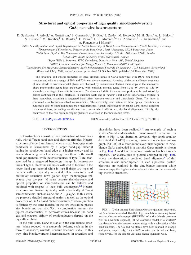
Structural and optical properties of high quality zinc-blende/wurtzite GaAs nanowire heterostructures D. Spirkoska, 1 J. Arbiol, 2 A. Gustafsson, 3 S. Conesa-Boj, 2 F. Glas, 4 I. Zardo, 1 M. Heigoldt, 1 M. H. Gass, 5 A. L. Bleloch, 5 S. Estrade, 2 M. Kaniber, 1 J. Rossler, 1 F. Peiro, 2 J. R. Morante, 2,6 G. Abstreiter, 1 L. Samuelson, 3 and A. Fontcuberta i Morral 1,7 1 Walter Schottky Institut and Physik Department, Technical University of Munich, Am Coulombwall 3, 85748 Garching, Germany 2 Departament d’Electrònica, Universitat de Barcelona, Marti i Franques, 08028 Barcelona, Spain 3 Solid State Physics, The Nanometer Consortium, Lund University, P.O. Box 118, Lund 22100, Sweden 4 CNRS-LPN, Route de Nozay, 91460 Marcoussis, France 5 SuperSTEM Laboratory, STFC Daresbury, Daresbury WA4 4AD, United Kingdom 6 IREC, Catalonia Institute for Energy Research, Barcelona 08019, CAT, Spain 7 Laboratoire des Matériaux Semiconducteurs, Ecole Polytechnique Fédérale de Lausanne, 1015 Lausanne, Switzerland Received 8 July 2009; revised manuscript received 29 October 2009; published 31 December 2009 The structural and optical properties of three different kinds of GaAs nanowires with 100% zinc-blende structure and with an average of 30% and 70% wurtzite are presented. A variety of shorter and longer segments of zinc-blende or wurtzite crystal phases are observed by transmission electron microscopy in the nanowires. Sharp photoluminescence lines are observed with emission energies tuned from 1.515 eV down to 1.43 eV when the percentage of wurtzite is increased. The downward shift of the emission peaks can be understood by carrier confinement at the interfaces, in quantum wells and in random short period superlattices existent in these nanowires, assuming a staggered band offset between wurtzite and zinc-blende GaAs. The latter is confirmed also by time-resolved measurements. The extremely local nature of these optical transitions is evidenced also by cathodoluminescence measurements. Raman spectroscopy on single wires shows different strain conditions, depending on the wurtzite content which affects also the band alignments. Finally, the occurrence of the two crystallographic phases is discussed in thermodynamic terms. DOI: 10.1103/PhysRevB.80.245325 PACS numbers: 61.46.Km, 78.55.Cr, 68.37.Og, 78.60.Hk I. INTRODUCTION Heterostructures consist of the combination of two mate- rials, with different band gaps and electron affinities. Hetero- structures of type I are formed when a small band-gap semi- conductor is surrounded by a larger band-gap material having its conduction-band edge at a higher energy and its valence-band edge at a lower energy than those in the small band-gap material while heterostructures of type II are char- acterized by a staggered band-edge lineup. In heterostruc- tures of type I, electrons and holes will tend to localize in the lower band-gap material while in type II these two types of carriers will be spatially separated. Heterostructures and multilayer structures have gained huge technological rel- evance over the past 40 years because the electronic and optical properties of semiconductors can be tailored and modified with respect to their bulk counterpart. 1,2 Hetero- structures are formed typically with chemically different semiconductors, such as GaAs and Al 1-x Ga x As. In this work, we present a detailed structural analysis as well as the optical properties of GaAs based “heterostructures,” whose junction is formed by the same material in the two crystalline phases zinc blende and wurtzite. Such a combination presents the typical characteristics of heterostructures because the band gap and electron affinity of semiconductors depend on the crystalline phase. In the bulk state, GaAs is stable in the zinc-blende struc- ture. When reduced to a nanoscale volume, such as in the form of nanowire, wurtzite structure becomes stable. In this way, zinc-blende/wurtzite heterostructures in arsenides and phosphides have been realized. 3–8 An example of such a wurtzite/zinc-blende/wurtzite quantum-well structure is given in Fig. 1. An aberration corrected high angle annular dark field HAADF scanning transmission electron micro- graph STEM of a three-monolayer-thick segment of zinc- blende GaAs embedded in a wurtzite GaAs matrix is shown in Fig. 1a. A model of the atomic positions has been super- imposed. For clarity, this is plotted enlarged in Fig. 1b, where the theoretically predicted band alignment 9 of this structure is also superimposed. In such a potential profile, electrons are confined in the zinc-blende segment while holes occupy the higher valence-band states in the surround- ing wurtzite structures. FIG. 1. Color online Zinc-blende/wurtzite quantum structures. a Aberration corrected HAADF high resolution scanning trans- mission electron micrograph HRSTEM of a zinc-blende quantum well in a wurtzite segment. b An atomistic model of a wurtzite/ zinc-blende/wurtzite heterostructure along with a schematics of the band diagram. The Ga and As atoms have been marked in orange and green, respectively, for the WZ domains, and in red and blue, respectively, for the double unit zinc-blende quantum well. PHYSICAL REVIEW B 80, 245325 2009 1098-0121/2009/8024/2453259 ©2009 The American Physical Society 245325-1
Transcript of Structural and optical properties of high-quality ZnTe homoepitaxial layers
Structural and optical properties of high quality zinc-blende/wurtziteGaAs nanowire heterostructures
D. Spirkoska,1 J. Arbiol,2 A. Gustafsson,3 S. Conesa-Boj,2 F. Glas,4 I. Zardo,1 M. Heigoldt,1 M. H. Gass,5 A. L. Bleloch,5
S. Estrade,2 M. Kaniber,1 J. Rossler,1 F. Peiro,2 J. R. Morante,2,6 G. Abstreiter,1 L. Samuelson,3 andA. Fontcuberta i Morral1,7
1Walter Schottky Institut and Physik Department, Technical University of Munich, Am Coulombwall 3, 85748 Garching, Germany2Departament d’Electrònica, Universitat de Barcelona, Marti i Franques, 08028 Barcelona, Spain
3Solid State Physics, The Nanometer Consortium, Lund University, P.O. Box 118, Lund 22100, Sweden4CNRS-LPN, Route de Nozay, 91460 Marcoussis, France
5SuperSTEM Laboratory, STFC Daresbury, Daresbury WA4 4AD, United Kingdom6IREC, Catalonia Institute for Energy Research, Barcelona 08019, CAT, Spain
7Laboratoire des Matériaux Semiconducteurs, Ecole Polytechnique Fédérale de Lausanne, 1015 Lausanne, Switzerland�Received 8 July 2009; revised manuscript received 29 October 2009; published 31 December 2009�
The structural and optical properties of three different kinds of GaAs nanowires with 100% zinc-blendestructure and with an average of 30% and 70% wurtzite are presented. A variety of shorter and longer segmentsof zinc-blende or wurtzite crystal phases are observed by transmission electron microscopy in the nanowires.Sharp photoluminescence lines are observed with emission energies tuned from 1.515 eV down to 1.43 eVwhen the percentage of wurtzite is increased. The downward shift of the emission peaks can be understood bycarrier confinement at the interfaces, in quantum wells and in random short period superlattices existent inthese nanowires, assuming a staggered band offset between wurtzite and zinc-blende GaAs. The latter isconfirmed also by time-resolved measurements. The extremely local nature of these optical transitions isevidenced also by cathodoluminescence measurements. Raman spectroscopy on single wires shows differentstrain conditions, depending on the wurtzite content which affects also the band alignments. Finally, theoccurrence of the two crystallographic phases is discussed in thermodynamic terms.
DOI: 10.1103/PhysRevB.80.245325 PACS number�s�: 61.46.Km, 78.55.Cr, 68.37.Og, 78.60.Hk
I. INTRODUCTION
Heterostructures consist of the combination of two mate-rials, with different band gaps and electron affinities. Hetero-structures of type I are formed when a small band-gap semi-conductor is surrounded by a larger band-gap materialhaving its conduction-band edge at a higher energy and itsvalence-band edge at a lower energy than those in the smallband-gap material while heterostructures of type II are char-acterized by a staggered band-edge lineup. In heterostruc-tures of type I, electrons and holes will tend to localize in thelower band-gap material while in type II these two types ofcarriers will be spatially separated. Heterostructures andmultilayer structures have gained huge technological rel-evance over the past 40 years because the electronic andoptical properties of semiconductors can be tailored andmodified with respect to their bulk counterpart.1,2 Hetero-structures are formed typically with chemically differentsemiconductors, such as GaAs and Al1−xGaxAs. In this work,we present a detailed structural analysis as well as the opticalproperties of GaAs based “heterostructures,” whose junctionis formed by the same material in the two crystalline phaseszinc blende and wurtzite. Such a combination presents thetypical characteristics of heterostructures because the bandgap and electron affinity of semiconductors depend on thecrystalline phase.
In the bulk state, GaAs is stable in the zinc-blende struc-ture. When reduced to a nanoscale volume, such as in theform of nanowire, wurtzite structure becomes stable. In thisway, zinc-blende/wurtzite heterostructures in arsenides and
phosphides have been realized.3–8 An example of such awurtzite/zinc-blende/wurtzite quantum-well structure isgiven in Fig. 1. An aberration corrected high angle annulardark field �HAADF� scanning transmission electron micro-graph �STEM� of a three-monolayer-thick segment of zinc-blende GaAs embedded in a wurtzite GaAs matrix is shownin Fig. 1�a�. A model of the atomic positions has been super-imposed. For clarity, this is plotted enlarged in Fig. 1�b�,where the theoretically predicted band alignment9 of thisstructure is also superimposed. In such a potential profile,electrons are confined in the zinc-blende segment whileholes occupy the higher valence-band states in the surround-ing wurtzite structures.
FIG. 1. �Color online� Zinc-blende/wurtzite quantum structures.�a� Aberration corrected HAADF high resolution scanning trans-mission electron micrograph �HRSTEM� of a zinc-blende quantumwell in a wurtzite segment. �b� An atomistic model of a wurtzite/zinc-blende/wurtzite heterostructure along with a schematics of theband diagram. The Ga and As atoms have been marked in orangeand green, respectively, for the WZ domains, and in red and blue,respectively, for the double unit zinc-blende quantum well.
PHYSICAL REVIEW B 80, 245325 �2009�
1098-0121/2009/80�24�/245325�9� ©2009 The American Physical Society245325-1
The most successful synthesis method of semiconductornanowires has made use of the vapor-liquid-solid mechanismin which the reactants are supplied in the vapor phase anddecomposed and/or directly incorporated in a metal seed.10
The thermodynamics of two-dimensional �2D� nucleation ofthe seeds at the interface between the catalyst droplet and thesolid nanowire determines the crystalline quality of thenanowires.11 In general, the existence of crystal imperfec-tions in semiconductors limits the expected performance ofoptoelectronic devices. Crystalline imperfections introducedduring growth of III-V semiconductor nanowires such as InPand GaAs are very common and include rotational twinsand polytypism between wurtzite and zinc-blendestructures.8,12–17 From the crystallographic point of view,zinc-blende and wurtzite structures differ only in the stackingperiodicity of the �111�ZB / �0010�WZ oriented planes.18–20
From the fundamental point of view, the occurrence of poly-typism in III-V nanowires is particularly interesting. As thewurtzite phase is not stable in the bulk form, the electricaland optical properties are not well known. Twinning orwurtzite/zinc-blende nanowire heterostructures or superlat-tices should result in a modification of the band structure,generating new forms of band offsets and electronic mini-bands in a chemically homogeneous material such asGaAs.21,22 In some cases, the existence of this crystal phaseheterostructure has been denominated as the formation ofcrystal phase quantum dots in the nanowires.23 From thetechnological point of view, achieving control of thewurtzite/zinc-blende phases in nanowires may enable thefabrication of new kinds of devices such as quantum wirecascade lasers.24
The occurrence of wurtzite structure as one of the maincrystalline phases of III-V nanowires has been discussed byseveral authors. From the thermodynamic point of view, thesurface energy of �1100� wurtzite planes might be low incomparison with �110� and �111�A /B of zinc blende, al-though detailed atomistic calculations are still lacking. As aconsequence, for small radii nanowires, the wurtzite phasewould be more stable than the zinc blende. In the case ofGaAs, the critical radius under which wurtzite is expected tobe the most stable phase lies between 5 and 25.5 nm, de-pending on the theory.25–27 Other thermodynamic consider-ations relate the formation of wurtzite nanowires with a highsupersaturation in the catalyst. As nanowires do not growunder thermodynamic equilibrium conditions, kinetic theo-ries have also been used to understand the occurrence ofwurtzite nanowires. These theories indicate that the nucle-ation of new crystalline layers in the nanowire occurs at thetriple phase line.19,28 This type of nucleation kinetically fa-vors crystalline structures exhibiting minimal surface energyfacets, again in favor of the wurtzite structure. It is importantto note that none of these works refer to nanowire grownwithout using gold. The optical properties of wurtzite/zinc-blende structures have been investigated in the past by pho-toluminescence �PL� spectroscopy. To date, relatively broadspectra have been obtained, which do not elucidate the quan-tum nature of these structures.29,30
In this work, we present structural and optical propertiesof very clean GaAs zinc-blende/wurtzite nanowires hetero-structures with different average contents of wurtzite phases
exhibiting localized and sharp emission characteristics.Thanks to the use of local spectroscopy and time-resolvedtechniques such as confocal photoluminescence and cathod-oluminescence �CL�, the quantum confined nature of theseheterostructures is elucidated. The optical characterization isaccompanied with Raman spectroscopy in order to reveal thepresence of strain. Some theoretical considerations on thegrowth mechanisms of each of the crystalline phases are alsoincluded.
II. EXPERIMENTAL DETAILS
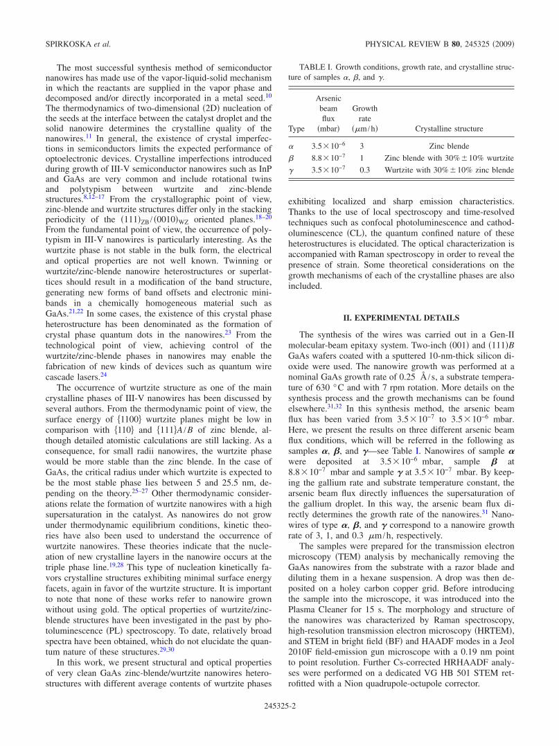
The synthesis of the wires was carried out in a Gen-IImolecular-beam epitaxy system. Two-inch �001� and �111�BGaAs wafers coated with a sputtered 10-nm-thick silicon di-oxide were used. The nanowire growth was performed at anominal GaAs growth rate of 0.25 Å /s, a substrate tempera-ture of 630 °C and with 7 rpm rotation. More details on thesynthesis process and the growth mechanisms can be foundelsewhere.31,32 In this synthesis method, the arsenic beamflux has been varied from 3.5�10−7 to 3.5�10−6 mbar.Here, we present the results on three different arsenic beamflux conditions, which will be referred in the following assamples �, �, and �—see Table I. Nanowires of sample �were deposited at 3.5�10−6 mbar, sample � at8.8�10−7 mbar and sample � at 3.5�10−7 mbar. By keep-ing the gallium rate and substrate temperature constant, thearsenic beam flux directly influences the supersaturation ofthe gallium droplet. In this way, the arsenic beam flux di-rectly determines the growth rate of the nanowires.31 Nano-wires of type �, �, and � correspond to a nanowire growthrate of 3, 1, and 0.3 �m /h, respectively.
The samples were prepared for the transmission electronmicroscopy �TEM� analysis by mechanically removing theGaAs nanowires from the substrate with a razor blade anddiluting them in a hexane suspension. A drop was then de-posited on a holey carbon copper grid. Before introducingthe sample into the microscope, it was introduced into thePlasma Cleaner for 15 s. The morphology and structure ofthe nanowires was characterized by Raman spectroscopy,high-resolution transmission electron microscopy �HRTEM�,and STEM in bright field �BF� and HAADF modes in a Jeol2010F field-emission gun microscope with a 0.19 nm pointto point resolution. Further Cs-corrected HRHAADF analy-ses were performed on a dedicated VG HB 501 STEM ret-rofitted with a Nion quadrupole-octupole corrector.
TABLE I. Growth conditions, growth rate, and crystalline struc-ture of samples �, �, and �.
Type
Arsenicbeamflux
�mbar�
Growthrate
��m /h� Crystalline structure
� 3.5�10−6 3 Zinc blende
� 8.8�10−7 1 Zinc blende with 30%�10% wurtzite
� 3.5�10−7 0.3 Wurtzite with 30%�10% zinc blende
SPIRKOSKA et al. PHYSICAL REVIEW B 80, 245325 �2009�
245325-2

The optical properties were investigated by PL and CLspectroscopy at the single nanowire level. PL spectroscopyexperiments on single nanowires were carried out by the useof a confocal microscope embedded in a He4 cryostat.33 Thesamples could be scanned below the confocal objective�NA=0.65� with piezopositioners with a spatial accuracy inthe nanometer range. The measurements were realized at atemperature of 4.2 K, using the 632.8 nm line of a He-Nelaser as an excitation source. The spot size of the laser in theconfocal microscope is about 0.8 �m. The luminescencewas detected and analyzed by the combination of a gratingspectrometer and Si charge coupled device. The spectrometerhas a resolution of 500 �eV. In order to avoid interferenceof the PL signal with the underlying GaAs substrate, thenanowires were first mechanically removed from the initialsubstrate and transferred in low densities to an oxidizedpiece of silicon. Single nanowires could be localized on thesurface by scanning reflectivity measurements over areas ofup to 30 �m. Time-resolved measurements were realized byexciting with a Ti:sapphire laser and detecting the photolu-minescence intensity as a function of time with a photomul-tiplier. The laser-pulse width and repetition rate were 100 psand 12 ns, respectively.
For CL measurements, the samples were prepared in asimilar way on a gold coated silicon substrate—gold ensuresa good extraction of the impinging electrons such that nocharging occurs. CL was realized in an adapted scanningelectron microscope. The luminescence was detected andanalyzed by the combination of a grating spectrometer and aphotomultiplier. The temperature of the sample was 10 K.The beam was focused to a small spot of 50 nm in diameterand was scanned over the sample in order to obtain a map ofthe spectral variations along the sample. More details on thetechnique can be found in Ref. 34.
Spatially resolved Raman spectroscopy was realized witha �-Raman setup in the backscattering configuration onsingle GaAs nanowires transferred on to a silicon substrate.Prior to the measurements, the nanowires were identified onthe substrate by imaging the surface with a camera. The ex-citation wavelength was the 514.5 nm line of the Ar+ laser.The used laser power of the excitation was about 200 �W�equivalent to 70 kW /cm−2�, in order to avoid heating of thenanowire.35 The scattered light was collected by an XY Ra-man Dilor triple spectrometer with a multichannel chargecouple device detector. The sample was positioned on a XYpiezostage, which allowed the scanning of the surface �andtherefore the nanowire� with a precision of 10 nm.
III. EXPERIMENTAL RESULTS
A. Crystalline structure
The crystalline structure of the samples type �, �, and �were analyzed by HRTEM and Cs-corrected HRSTEM inHAADF mode. This method has the advantage that the in-tensity maxima in the micrographs correspond to the atomicpositions. Additionally, the observed intensity is nearly pro-portional to the square of the average atomic number of theelements constituting the atomic column. We observe thatnanowires grown under conditions �—highest growth rate—
are composed of a single zinc-blende structure while nano-wires synthesized under conditions � and � have an increas-ing percentage of the wurtzite phase. Remarkably, the typicalzigzag shape of twinned zinc-blende nanowires was ob-served in none of the conditions here reported.36 A typicallow-resolution TEM measurement of a pure zinc-blendenanowire is shown in Fig. 2�a�. The lateral facets of thesenanowires are of the �110� crystallographic family.37 Somestripes of different contrast with thickness on the order of100 nm are observed. The periodicity of these zones can varyalong the nanowire and is typically higher for the initial andfinal stages of growth, as shown in Fig. 2�b�. These stripesare caused by a rotational twinning, a 180° rotation aroundthe growth axis. A high-resolution TEM analysis of one suchtwin interface is shown in Fig. 2�c�.
A quite different structure is observed for nanowires ob-tained under growth conditions � and �. For these wires, weobserve the existence of different sections with wurtzite andzinc-blende structures. Before we proceed with the statisticalanalysis of the structure, we present a precise structuralanalysis of the zinc-blende and wurtzite sections. A high-resolution TEM image of the nanowire obtained under con-ditions � is shown in Fig. 2�d�. A HAADF image of the sameregion is superimposed onto the micrograph. Figure 2�e�shows a magnified image of the boxed region in Fig. 2�d�. Adouble twinned interface between two wurtzite domains re-sults in a region composed of two zinc-blende unit cells.Twinned planes have been marked with dashed lines whileGa and As atoms have been marked in orange and green,respectively, for the wurtzite domains, and in red and blue,respectively, for the double unit zinc-blende-cell quantumwell. As can be seen clearly in the sketch, a 180° rotationaltwin in the zinc-blende structure creates the equivalent stack-ing of a single wurtzite unit in the interface. Two consecutivetwins create an atomic stacking corresponding to two wurtz-ite unit cells and so on. Following the same model, a 180°rotational twin in the wurtzite structure would lead to theformation of one GaAs unit cell of zinc blende—a rotationaltwin in wurtzite corresponds to a stacking ofABABCBCBCB. The atomic arrangement in the wurtzite/zinc-blende heterostructure shown in Figs. 2�d� and 2�e� issuperimposed in Fig. 2�e� so that the different stacking of theplanes becomes obvious.
In order to quantify the occurrence of wurtzite structure asa function of the growth conditions, a detailed statisticalanalysis of many nanowires was realized. In general, thestructural properties of the nanowires obtained under thesame conditions were very similar. The exact stacking be-tween wurtzite and zinc-blende layers was found to differ butthe average occurrence coincides. Nanowires of type � typi-cally presented four parts, with different ratios of wurtzite-zinc-blende phases. HRTEM micrographs of these four partsare shown in Fig. 3. In order to identify the two crystallinephases, we have used a color code. Red denotes wurtzitewhile blue and green refer to the two twinned orientations ofzinc blende. In Fig. 3�a� the structure of top part of the nano-wire is presented. Typically, the nanowires grown underthese conditions finish with the zinc-blende structure. Thedensity of twins is relatively high, the typical intertwin dis-tance about 10 nm. Below this zinc-blende structure that has
STRUCTURAL AND OPTICAL PROPERTIES OF HIGH… PHYSICAL REVIEW B 80, 245325 �2009�
245325-3

an extension of about 1 �m, a zone composed of an alter-nation of zinc-blende and wurtzite domains is observed �Fig.3�b��. The domains/regions have a thickness between 5 and 1nm. This section extends about 0.8 �m on the nanowire.Below this region, the wurtzite sections increase in thicknessup to 10 nm and the presence of zinc blende is graduallyreduced as it is shown in Figs. 3�c� and 3�d�. Overall, the partor the nanowire exhibiting wurtzite structure representsabout 30%�10% of wurtzite phases.
Nanowires grown under � conditions exhibit a muchhigher percentage of wurtzite structure. Typical HRTEM mi-crographs of the different sections of the nanowire are shownin Fig. 4. There, the growth of the nanowire also ends with azinc-blende structure. This time the zone with pure zinc-blende structure is only about 50 nm long. Details on thezinc-blende section are shown in Fig. 4�b�. As shown in thedetailed micrographs of Figs. 4�c�–4�e�, below this initialsection the percentage of wurtzite is very high. There areregions with a high-frequency alternation between wurtziteand zinc-blende phases forming a kind of random superlat-tice and others with extremely thin inclusions of zinc-blendelayers in wurtzite �narrow quantum wells�. We estimate thatthe proportion of wurtzite phase under these growth condi-tions is about 70%�10%.
B. Optical properties
The optical properties of the three types of nanowireswere investigated by photoluminescence and cathodolumi-
nescence spectroscopy, respectively, at 4.2 and 10 K. TypicalPL measurements realized on single nanowires are presentedin Fig. 5. For illustration purposes, the spectra have beenshifted vertically by adding an offset. PL spectrum of nano-wires type � corresponds to the top spectrum of the figure.As expected, nanowires from sample � exhibit a single PLpeak which corresponds to the free exciton luminescence ofGaAs at 1.515 eV. The PL characteristics of the other
FIG. 2. �Color� Transmission electron microscopy of GaAsnanowires presenting different crystalline structures. For illustrationpurposes, we have indicated each orientation of the zinc-blendephase domains with blue and green circles, and the wurtzite phaseregions with red circles. �a� General view of the high beam fluxnanowires �conditions �� presenting twins in the zinc-blende struc-ture. �b� Detail of the twin zinc-blende domains. �c� HRTEM analy-sis of a twin interface. �d� HRTEM detail of a nanowire synthesizedunder conditions �. Inset in �d� corresponds to an aberration cor-rected HAADF HRSTEM image of the same region. �e� MagnifiedCs-corrected HAADF HRSTEM detail of the squared region in �d�.A zinc-blende quantum well embedded between two wurtzite re-gions. Twinned planes have been marked with dashed lines. Simu-lation of the atomic positions has been superimposed on themeasurement.
FIG. 3. �Color� Transmission electron micrograph from differentsegments of a single GaAs nanowires type �. From �a� to �d�, thesections belong to different regions of the nanowire from the tip tobottom, corresponding, respectively, from the latest to initial part ofthe growth process. The red spots correspond to regions with wurtz-ite structure while the blue and green spots correspond to regionswith zinc-blend structure—with the two twin orientations.
FIG. 4. �Color� Transmission electron micrograph from GaAsnanowire grown under As BF of 3.5�10−7 mbar—type �. Thesmall insets show closer view of the structure from the selectedregions.
SPIRKOSKA et al. PHYSICAL REVIEW B 80, 245325 �2009�
245325-4

samples are quite different from sample type �—pure zincblende. A large downward shift of the photoluminescenceand an increased number of sharp peaks are observed fornanowires of samples � and �. For sample �, several well-defined peaks are present at positions between 1.51 and 1.46eV, with a full width at half maximum between 2 and 6 meVwith some peaks even much sharper. In the case of sample �,a similar number of peaks is observed but downshifted to theenergy range between 1.47 and 1.43 eV. No free exciton lineof the zinc-blende phase is observed in these wires.
PL measurements have been performed on various othernanowires corresponding to the growth conditions � and �.The spectra are in all cases very similar. Several lumines-cence peaks in the ranges 1.51–1.46 eV for sample � and1.47–1.43 eV for sample � are observed. The exact positionand intensity of each peak varies from sample to sample andon the position on the nanowire. These results are in agree-ment with the fact that the structure varies along the axis ofthe nanowires. Additionally, the exact sequence of wurtziteand zinc-blende sections varies from wire to wire. In order toillustrate this, scanning confocal photoluminescence mea-surements of one sample of each of the �, �, and � types arepresented in Figs. 6�a�–6�c�, respectively. The PL emissionof sample � is rather homogeneous along the wire, withsome variations in intensity and linewidth, but altogetherconsistent with pure zinc-blende GaAs. A single peak at1.515 eV is observed, which corresponds to the free excitonline of zinc-blende GaAs.38 Sample � exhibits many morespectral features in the energy range between 1.515 and 1.46eV. The spectral features are not homogeneous along thelength. At the top part of the scan, the luminescence isbrighter than at the bottom part. The free exciton peak at1.515 eV is present in only some regions of the nanowirewhile lower energy peaks are observed over the wholelength. The presence of the various peaks depends on theposition on the nanowire. This may be understood by the
variation in the structure along the wire as presented in Sec.III A. In the wire of type � we find that only one part of thenanowire shows luminescence peaks, with spectral featuresbetween 1.48 and 1.43 eV. Each of the peaks is located indifferent regions of the nanowire. It is interesting to note thatno PL signal is observed in the top part of the scan up to 1.55eV—the region between 1.53 and 1.55 eV not shown in thefigure.
Before going into detail of the analysis of the PL mea-surements, we present the results on cathodoluminescencespectroscopy mapping �Fig. 7�. A series of monochromaticcathodoluminescence images of several nanowires of asample of type � was recorded. These nanowires show anemission pattern at energies between 1.51 and 1.46 eV.Monochromatic images in this energy range exhibit a seriesof spatially localized bright emission spots, as illustrated inFigs. 7�b�–7�e�. These spots appear at different positionsalong the wire for different energies. By comparing the pat-terns in the monochromatic images, like in Fig. 7�e�, we
FIG. 5. �Color online� Typical photoluminescence spectra ob-served from the three types of nanowires at T=4.2 K. The spectrahave been obtained from single wires under illumination at 632.8nm with a power density of 2.5 W /cm2. The synthesis conditionsfor samples �, �, and � can be found in Table I. The emissionenergy shifts from 1.51 eV down to 1.43 eV depending on thegrowth conditions which result in different proportion of wurtziteand zinc-blende GaAs.
FIG. 6. �Color online� Spatially resolved confocal photolumi-nescence measurements along one single nanowire. The spectra cor-respond to sample type �a� �, �b� �, and �c� �.
STRUCTURAL AND OPTICAL PROPERTIES OF HIGH… PHYSICAL REVIEW B 80, 245325 �2009�
245325-5

conclude that the different emission energies originate fromdifferent locations in the nanowire. By analyzing the inten-sity profiles, we can conclude that the carrier diffusion lengthis very short, less than 100 nm. These characteristics advo-cate highly for the existence of an array of quantum hetero-structures with different quantization energies along thenanowire. The cathodoluminescence of sample � is also pro-vided for reference in Fig. 7�g�. These nanowires show emis-sion related to the free exciton of zinc-blende GaAs frommost of its length. This is in good agreement with the HR-TEM measurements and the spatially resolved photolumines-cence studies presented above.
IV. DISCUSSION
A. Evidence for staggered band offsets
The photoluminescence peaks and cathodoluminescencemaps presented in Figs. 5–7 can be interpreted based on thetheoretical band gaps and the band alignment in wurtzite/zinc-blende heterostructures.9 The energy gap of unstrainedwurtzite GaAs was predicted to be about 33 meV higher thanthat of zinc blende.9 This has been verified recently with PLmeasurements of pure wurtzite nanowires.3 Wurtzite/zinc-blende GaAs heterostructures are believed to exhibit a type IIband alignment as shown schematically in Figs. 1�b� and8�a�. Theory predicts conduction and valence-band disconti-nuities of 117 and 84 meV, respectively, where the valenceband is higher in wurtzite.9 Effects of strain and spontaneouspolarization at the wurtzite/zincblende interface are ne-glected. With this simple model it is expected that anelectron-hole pair confined to the wurtzite/zinc-blende inter-face will give rise to a spatially indirect recombination at1.431 eV neglecting also the exciton binding energy, whichis expected to be small due to the spatially indirect nature ofthe exciton. This spatially indirect recombination should be
the lowest energy observable in pure GaAs wurtzite/zinc-blende multilayer structures. Indeed we observe in wires oftype � the lowest PL line typically at 1.43 eV, in excellentagreement with our simple model. When the thickness ofwurtzite and zinc-blende regions are reduced to several na-nometers, quantum wells are formed and quantized levels ofelectrons and holes appear. Some examples of such type ofmultilayer structures are sketched in Fig. 8�a�. As a conse-quence of the type II band alignment, electrons and holes arespatially separated and stored in the zinc-blende and wurtziteregions, respectively. The thinner the quantum well, thehigher is the quantization energy and PL lines are expectedbetween 1. 515 and 1.43 eV. In the case where the wurtzitesections are long enough, one would also expect to observeluminescence from this phase at about 1.55 eV.39
We have calculated the first electron and hole confinedstates of a wurtzite or zinc-blende quantum well embeddedin a zinc-blende or wurtzite matrix, respectively. These cal-culations are indicative and have been realized by assumingthe same effective masses for the two GaAs polytypes ofelectrons and holes, respectively. The energy values are plot-
A
C
B
F G
D
E
1.0 µm
1.0 µm
1.485 eV
SEM
1.0 µm
SEM
1.515 eV1.485 eV1.459 eV
1.514 eV
1.510 eV
1.459 eV
FIG. 7. �Color� Cathodoluminescence of wurtzite/zinc-blendeheterostructures. Scanning electron microscopy and monochromaticcathodoluminescence images of nanowires synthesized under con-ditions � and �. A shows an SEM image of a nanowire of type �and �b�–�d� shows the corresponding CL images recorded at differ-ent energies, illustrating the different spatial origin of the variousemission energies. This is even clearer in the composite image of�e�. For comparison, we also show images of nanowires type �. F isan SEM image and G the corresponding 1.51 eV CL image, show-ing homogeneous emission along the length of the nanowire.
FIG. 8. �Color online� �a� The theoretical band alignment ofwurtzite and zinc-blende GaAs, along with the values ofconduction-band and valence-band discontinuities are shown. Someselected examples of quantum heterostructures which are presented,along with the first quantized level as calculated in �b�. The relativescale in energy and length has been kept. The first quantized energylevels sketched correspond to quantum wells of 7.5, 5, and 2.5 nm.Due to the type II alignment, the holes are confined in the wurtzitequantum wells while the electrons are confined in the zinc-blendequantum wells. In �b�, plot of the energy positions of the first elec-tron �E1C� and hole �E1V� levels of quantum wells as a function ofthe quantum well thickness.
SPIRKOSKA et al. PHYSICAL REVIEW B 80, 245325 �2009�
245325-6
ted in Fig. 8�b�. Due to the smaller mass of the electroncompared to the hole and the higher conduction-band discon-tinuity, the confinement energy is larger for electrons than forholes. Following these calculations, as the thickness of thequantum wells is reduced to zero, the first level of the elec-tron and hole states tends to the value of the conduction-bandand valence-band offsets. Experimentally, we observe thatwires of type � show PL lines at higher energies closer to thezinc-blende free exciton line while PL lines in the lowerenergy range are observed with increasing wurtzite content�samples ��. This cannot be explained with the simple con-finement model presented above. However, one should notethat on the nanowire sections where the wurtzite and zinc-blende regions are below �3 nm, the quantum wells are notisolated but highly frequent. We believe that in these regions,the electron and hole wave functions overlap and form mini-bands that reduce the value of the confinement energy.24,40
Such kinds of random superlattices are indeed observed inthe TEM analysis of the wires, as shown in Fig. 3�b�.
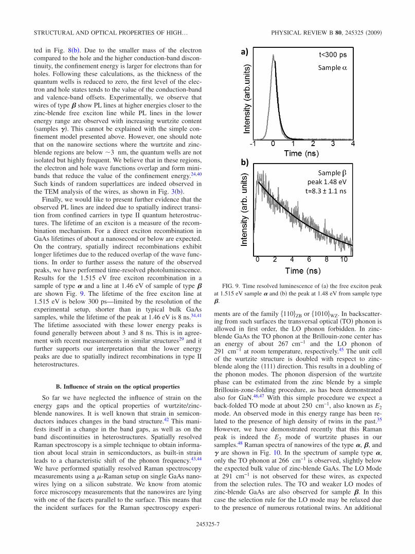
Finally, we would like to present further evidence that theobserved PL lines are indeed due to spatially indirect transi-tion from confined carriers in type II quantum heterostruc-tures. The lifetime of an exciton is a measure of the recom-bination mechanism. For a direct exciton recombination inGaAs lifetimes of about a nanosecond or below are expected.On the contrary, spatially indirect recombinations exhibitlonger lifetimes due to the reduced overlap of the wave func-tions. In order to further assess the nature of the observedpeaks, we have performed time-resolved photoluminescence.Results for the 1.515 eV free exciton recombination in asample of type � and a line at 1.46 eV of sample of type �are shown Fig. 9. The lifetime of the free exciton line at1.515 eV is below 300 ps—limited by the resolution of theexperimental setup, shorter than in typical bulk GaAssamples, while the lifetime of the peak at 1.46 eV is 8 ns.34,41
The lifetime associated with these lower energy peaks isfound generally between about 3 and 8 ns. This is in agree-ment with recent measurements in similar structures29 and itfurther supports our interpretation that the lower energypeaks are due to spatially indirect recombinations in type IIheterostructures.
B. Influence of strain on the optical properties
So far we have neglected the influence of strain on theenergy gaps and the optical properties of wurtzite/zinc-blende nanowires. It is well known that strain in semicon-ductors induces changes in the band structure.42 This mani-fests itself in a change in the band gaps, as well as on theband discontinuities in heterostructures. Spatially resolvedRaman spectroscopy is a simple technique to obtain informa-tion about local strain in semiconductors, as built-in strainleads to a characteristic shift of the phonon frequency.43,44
We have performed spatially resolved Raman spectroscopymeasurements using a �-Raman setup on single GaAs nano-wires lying on a silicon substrate. We know from atomicforce microscopy measurements that the nanowires are lyingwith one of the facets parallel to the surface. This means thatthe incident surfaces for the Raman spectroscopy experi-
ments are of the family �110�ZB or �1010�WZ. In backscatter-ing from such surfaces the transversal optical �TO� phonon isallowed in first order, the LO phonon forbidden. In zinc-blende GaAs the TO phonon at the Brillouin-zone center hasan energy of about 267 cm−1 and the LO phonon of291 cm−1 at room temperature, respectively.45 The unit cellof the wurtzite structure is doubled with respect to zinc-blende along the �111� direction. This results in a doubling ofthe phonon modes. The phonon dispersion of the wurtzitephase can be estimated from the zinc blende by a simpleBrillouin-zone-folding procedure, as has been demonstratedalso for GaN.46,47 With this simple procedure we expect aback-folded TO mode at about 250 cm−1, also known as E2mode. An observed mode in this energy range has been re-lated to the presence of high density of twins in the past.35
However, we have demonstrated recently that this Ramanpeak is indeed the E2 mode of wurtzite phases in oursamples.48 Raman spectra of nanowires of the type �, �, and� are shown in Fig. 10. In the spectrum of sample type �,only the TO phonon at 266 cm−1 is observed, slightly belowthe expected bulk value of zinc-blende GaAs. The LO Modeat 291 cm−1 is not observed for these wires, as expectedfrom the selection rules. The TO and weaker LO modes ofzinc-blende GaAs are also observed for sample �. In thiscase the selection rule for the LO mode may be relaxed dueto the presence of numerous rotational twins. An additional
FIG. 9. Time resolved luminescence of �a� the free exciton peakat 1.515 eV sample � and �b� the peak at 1.48 eV from sample type�.
STRUCTURAL AND OPTICAL PROPERTIES OF HIGH… PHYSICAL REVIEW B 80, 245325 �2009�
245325-7

peak is observed at 255 cm−1 that we attribute to the foldedTO phonon being at the zone center in the wurtzite structure,E2. This peak position is shifted slightly to higher wave num-bers than what it is expected from the back-folding model.For sample �, we also observe all three peaks. The peak ofwurtzite GaAs is stronger and it appears at the expected po-sition while the ones corresponding to zinc-blende GaAs areshifted 4 cm−1 to lower wave numbers, indicating the exis-tence of a tensile strain in the zinc-blende phase. Both theLO and TO are shifted by the same amount to lower wavenumbers, which is expected for small values of strain. Theexistence of strain in wurtzite/zinc-blende structures can beexplained by the difference in lattice constants of the twostructures.47 Therefore we expect compressive strain of thewurtzite segments in zinc-blende rich nanowires resulting ina blueshift of the E2 mode. Indeed we observe the wurtziterelated Raman mode at about 255 cm−1 in samples of type �instead of the expected 250 cm−1. On the other hand zinc-blende phases should be under more tensile strain inwurtzite-rich nanowires resulting in a redshift of the TO andLO modes, actually also observed in samples of type �. �Fig.10�. These results are strong evidence for different strainconditions in the wires of type � and �. Details of the Ra-man scattering on wurtzite/zinc-blende nanowires such as se-lection rules and polarization dependence of the phonon Ra-man modes are published elsewhere.48 It is well known thatthe band gaps decrease/increase with tensile/compressivestrain, respectively. In addition the band discontinuities varywith strain. Such effects may have non-negligible effect onthe luminescence lines observed in different energy regionsfor samples of type � and �.
C. Considerations on the occurrence of wurtziteand zinc-blende phases
Comparison of nanowires �, �, and � shows that, as theAs flux increases, the growth rate increases and the fractionof wurtzite material decreases—similarly, the decrease in thefraction of wurtzite toward the tops of nanowires � and � iscorrelated with some increase in the As flux during thegrowth of each nanowire. These findings are somewhat sur-prising since the growth rate is expected to increase with thesupersaturation—measured by the difference of chemical po-tential �� between liquid droplet and solid—and since, inAu-catalyzed GaAs nanowires, wurtzite has been demon-strated to form at high supersaturation and zinc blende atlower supersaturation.28
These seemingly contradictory observations might be rec-onciled as follows. According to the analysis of Ref. 28, thenucleation rate for each phase � is governed not only bysupersaturation but by the nucleation barrier �G���
2 /��,where �� is the effective edge energy of the 2D nucleus ofphase � that forms at the nanowire/droplet interface. Thisedge energy is expected to depend on the vapor pressure, inparticular, when nucleation happens at the triple phase line,28
where part of the edge is directly in contact with the vapor. Itmight thus happen that, as the As pressure is increased, thesupersaturation increases and the nucleation barriers �G� de-crease. As a consequence, the growth rate of the nanowireincreases, whereas the edge energies of the two phaseschange. This induces a change in �Gwz−�Gzb fromnegative-favoring wurtzite in nanowires � to positive-favoring zinc blende in nanowires �. This explanation re-mains highly speculative but the high density of phasechanges in nanowires � and � seem to indicate that thepresent conditions are indeed at the border of the zinc-blende/wurtzite transition. An alternative explanation wouldbe related to the position in which the nucleation events oc-cur. Nucleation at the triple phase line favors wurtzite whilenucleation away from the triple phase line favors zincblende. Indeed, as the supersaturation increases and the sizeof the critical nucleus decreases, the fraction of nucleationevents occurring at the triple phase line decreases at the ex-pense of those away from the triple phase line.19,28 Given thecomplexity of the system, it is clear that more extended stud-ies on the growth mechanisms need to be realized in thefuture, in order to obtain a more general theory accountingfor the existence of wurtzite and zinc-blende III-V semicon-ductors in the form of nanowires.
V. CONCLUSIONS
In conclusion, we have synthesized GaAs nanowires bymolecular-beam epitaxy under three different supersaturationconditions. We have obtained several GaAs polytypes rang-ing from pure zinc-blende to wurtzite-rich zinc-blende/wurtzite heterostructures, as demonstrated by HRTEM. Pho-toluminescence spectroscopy studies of these nanowiresshow sharp lines whose emission energy shifts from 1.515eV down to 1.43 eV when the percentage of wurtzite mate-rial in the nanowire is increased. This is interpreted as evi-dence for type II band alignment at the wurtzite/zinc-blende
FIG. 10. �Color online� Typical Raman spectra of single GaAsnanowires transferred on a silicon substrate. The spectra belong tothe three types of nanowires synthesized at an arsenic beam flux of3.4�10−6 mbar ���, 8.8�10−7 mbar ���, and 3.5�10−7 mbar���. In sample � only the TO mode is observed, which correspondsto what is typically observed in backscattering from �110� zinc-blende GaAs surfaces. The LO phonon appears weakly for sample���, along with a mode at lower frequencies which corresponds tothe wurtzite mode. In sample �, the wurtzite related mode is stron-ger and shifted due to the existence of a larger proportion of wurtz-ite in the nanowires. Note that all zinc-blende related modes appearshifted to lower wave numbers due to the adaptation of the latticeparameter closer to wurtzite, when zinc blende is minoritary in thestructure.
SPIRKOSKA et al. PHYSICAL REVIEW B 80, 245325 �2009�
245325-8

interface. The results may open the possibility for structuralband-gap engineering of other III-V nanowires and increasethe engineering possibilities with nanowires.
ACKNOWLEDGMENTS
The authors would like to kindly thank T. Garma and M.Bichler for their experimental support. This research was
supported by Marie Curie Excellence Grant “SENFED” andthe DFG excellence initiative Nanosystems Initiative Munichand SFB 631. This work was also supported in part by theSwedish Foundation for Strategic Research �SSF�, the Swed-ish Research Council �VR�, and the Knut and Alice Wallen-berg Foundation �KAW�. Authors would like to thank theTEM facilities in the Serveis Cientificotècnics in Universitatde Barcelona.
1 H. Kroemer, Proc. IEEE 51, 1782 �1963�.2 S. M. Sze, Semiconductor Devices: Physics and Technology
�John Wiley & Sons, New Jersey, 1985�.3 T. B. Hoang, A. F. Moses, H. L. Zhou, D. L. Dheeraj, B. O.
Fimland, and H. Weman, Appl. Phys. Lett. 94, 133105 �2009�.4 J. Johansson, L. S. Karlsson, K. A. Dick, J. Bolinsson, B. A.
Wacaser, K. Deppert, and L. Samuelson, Cryst. Growth Des. 9,766 �2009�.
5 T. Akiyama, K. Nakamura, and T. Ito, Phys. Rev. B 73, 235308�2006�.
6 P. Mohan, J. Motohisa, and T. Fukui, Nanotechnology 16, 2903�2005�.
7 K. Tomioka, J. Motohisa, S. Hara, and T. Fukui, Jpn. J. Appl.Phys., Part 2 46, L1102 �2007�.
8 A. Mishra et al., Appl. Phys. Lett. 91, 263104 �2007�.9 M. Murayama and T. Nakayama, Phys. Rev. B 49, 4710 �1994�.
10 R. S. Wagner and W. C. Ellis, Appl. Phys. Lett. 4, 89 �1964�.11 B. A. Wacaser, K. A. Dick, J. Johansson, M. T. Borgstroem, K.
Deppert, and L. Samuelson, Adv. Mater. �Weinheim, Ger.� 21,153 �2009�.
12 R. Banerjee, A. Bhattacharya, A. Genc, and B. M. Arora, Philos.Mag. Lett. 86, 807 �2006�.
13 R. E. Algra, M. A. Verheijen, M. T. Borgström, L. F. Feiner, G.Immink, W. J. P. van Enckevort, E. Vlieg, and E. P. A. M.Bakkers, Nature �London� 456, 369 �2008�.
14 F. Jabeen, V. Grillo, S. Rubini, and F. Martelli, Nanotechnology19, 275711 �2008�.
15 J. Noborisaka, J. Motohisa, and T. Fukui, Appl. Phys. Lett. 86,213102 �2005�.
16 Q. Xiong, J. Wang, and P. C. Eklund, Nano Lett. 6, 2736 �2006�.17 J. Arbiol et al., Nanotechnology 20, 145704 �2009�.18 F. Glas, J. Appl. Phys. 104, 093520 �2008�.19 V. G. Dubrovskii, N. V. Sibirev, J. C. Harmand, and F. Glas,
Phys. Rev. B 78, 235301 �2008�.20 A. Fontcuberta i Morral, J. Arbiol, J. D. Prades, A. Cirera, and J.
R. Morante, Adv. Mater. �Weinheim, Ger.� 19, 1347 �2007�.21 Z. Ikonic, G. P. Srivastava, and J. C. Inkson, Phys. Rev. B 52,
14078 �1995�.22 Z. Ikonić, G. P. Srivastava, and J. C. Inkson, Phys. Rev. B 48,
17181 �1993�.23 V. Zwiller �private communication�.24 J. Faist, F. Capasso, D. L. Sivico, C. Sirtori, A. L. Hutchinson,
and A. Y. Cho, Science 264, 553 �1994�.25 N. Ghaderi, M. Peressi, and N. Bingelli, Front. Fund. Comp.
Phys. 1018, 193 �2008�.26 T. Akiyama, K. Sano, K. Nakamura, and T. Ito, Jpn. J. Appl.
Phys., Part 2 45, L275 �2006�.27 V. G. Dubrovskii and N. V. Sibirev, Phys. Rev. B 77, 035414
�2008�.28 F. Glas, J. C. Harmand, and G. Patriarche, Phys. Rev. Lett. 99,
146101 �2007�.29 K. Pemasiri, M. Montazeri, R. Gass, L. M. Smith, H. E. Jackson,
J. Yarrison-Rice, S. Paiman, Q. Gao, H. H. Tan, C. Jagadish, X.Zhang, and J. Zou, Nano Lett. 9, 648 �2009�.
30 J. Bao, D. C. Bell, F. Capasso, J. B. Wagner, T. Martensson, J.Tragardh, and L. Samuelson, Nano Lett. 8, 836 �2008�.
31 A. Fontcuberta i Morral, C. Colombo, G. Abstreiter, J. Arbiol,and J. R. Morante, Appl. Phys. Lett. 92, 063112 �2008�.
32 C. Colombo, D. Spirkoska, M. Frimmer, G. Abstreiter, and A.Fontcuberta i Morral, Phys. Rev. B 77, 155326 �2008�.
33 http://www.attocube.com/nanoSCOPY/CFM/cfmI.html34 A. Gustafsson, M. E. Pistol, L. Montelius, and L. Samuelson, J.
Appl. Phys. 84, 1715 �1998�.35 D. Spirkoska, G. Abstreiter, and A. Fontcuberta i Morral, Nano-
technology 19, 435704 �2008�.36 L. S. Karlsson, K. A. Dick, J. B. Wagner, J. O. Malm, K. Dep-
pert, L. Samuelson, and L. R. Wallenberg, Nanotechnology 18,485717 �2007�.
37 A. Fontcuberta i Morral, D. Spirkoska, J. Arbiol, M. Heigoldt, J.R. Morante, and G. Abstreiter, Small, 4, 899 �2008�; M.Heigoldt, J. Arbiol, D. Spirkoska, J. M. Rebled, S. Conesa-Boj,G. Abstreiter, F. Peiró, J. R. Morante, and A. Fontcuberta i Mor-ral, J. Mater. Chem. 19, 840 �2009�.
38 E. Grilli, M. Guzzi, R. Zamboni, and L. Pavesi, Phys. Rev. B 45,1638 �1992�.
39 We would like to note here that we never observed luminescencefrom the wurtzite phase, even from sample type �. We believethat this is due to the diffusion of the exciton from the wurtzitesections to locations of the nanowire with lower energies.
40 G. Bastard, Wave Mechanics Applied to Semiconductor Hetero-structures �Wiley-Interscience, New York, 1991�.
41 V. Srinivas, J. Hryniewicz, Y. J. Chen, and C. E. C. Wood, Phys.Rev. B 46, 10193 �1992�.
42 M. Grundmann, The Physics of Semiconductors �Springer-Verlag, Berlin, 2007�.
43 R. Schorer, E. Friess, K. Eberl, and G. Abstreiter, Phys. Rev. B44, 1772 �1991�.
44 R. Loudon, Adv. Phys. 13, 423 �1964�.45 A. Mooradian and G. B. Wright, Solid State Commun. 4, 431
�1966�.46 H. Harima, J. Phys.: Condens. Matter 14, R967 �2002�.47 C.-Y. Yeh, Z. W. Lu, S. Froyen, and A. Zunger, Phys. Rev. B 46,
10086 �1992�.48 I. Zardo, S. Conesa-Boj, F. Peiro, J. R. Morante, J. Arbiol, E.
Uccelli, G. Abstreiter, and A. Fontcuberta i Morral, Phys. Rev. B80, 245324 �2009�.
STRUCTURAL AND OPTICAL PROPERTIES OF HIGH… PHYSICAL REVIEW B 80, 245325 �2009�
245325-9