Thermal Annealing Effects on the Optical and Structural Properties of (100) GaAs1−xBix Layers...
9
This article appeared in a journal published by Elsevier. The attached copy is furnished to the author for internal non-commercial research and education use, including for instruction at the authors institution and sharing with colleagues. Other uses, including reproduction and distribution, or selling or licensing copies, or posting to personal, institutional or third party websites are prohibited. In most cases authors are permitted to post their version of the article (e.g. in Word or Tex form) to their personal website or institutional repository. Authors requiring further information regarding Elsevier’s archiving and manuscript policies are encouraged to visit: http://www.elsevier.com/authorsrights
Transcript of Thermal Annealing Effects on the Optical and Structural Properties of (100) GaAs1−xBix Layers...
This article appeared in a journal published by Elsevier. The attachedcopy is furnished to the author for internal non-commercial researchand education use, including for instruction at the authors institution
and sharing with colleagues.
Other uses, including reproduction and distribution, or selling orlicensing copies, or posting to personal, institutional or third party
websites are prohibited.
In most cases authors are permitted to post their version of thearticle (e.g. in Word or Tex form) to their personal website orinstitutional repository. Authors requiring further information
regarding Elsevier’s archiving and manuscript policies areencouraged to visit:
http://www.elsevier.com/authorsrights
Author's personal copy
Thermal annealing effects on the opticaland structural properties of (100) GaAs1�xBix
layers grown by Molecular Beam Epitaxy
O.M. Lemine a,⇑, A. Alkaoud a, H.V. Avanço Galeti b, V. Orsi Gordo c,Y. Galvão Gobato c, Houcine Bouzid d, A. Hajry d, M. Henini e
a Department of Physics, College of Sciences, Al imam Mohammad Ibn Saud Islamic University (IMSIU), Riyadh, 11623 Riyadh,Saudi Arabiab Departamento de Engenharia Elétrica, UFSCar, 13565-905 São Carlos, SP, Brazilc Departamento de Física, UFSCar, 13565-905 São Carlos, SP, Brazild Promising Centre for Sensors and Electronic Devices (PCSED), Najran University, P.O. Box 1988, Najran 11001, Saudi Arabiae School of Physics and Astronomy, Nottingham Nanotechnology and Nanoscience Center, University of Nottingham, NottinghamNG7 2RD, UK
a r t i c l e i n f o
Article history:Received 20 May 2013Received in revised form 24 September 2013Accepted 7 October 2013Available online 14 October 2013
Keywords:GaAsBi alloysPLMBEXRDTEM
a b s t r a c t
The effects of long time thermal annealing at 200 �C on the opticaland structural properties of GaAs1�xBix alloys were investigated byX-ray diffraction (XRD), field emission scanning electron micros-copy (FESEM), high resolution transmission electron microscopy(HRTEM) and photoluminescence (PL). FESEM images show thatbismuth islands nucleate on the surface and their diameterincreases after annealing. It was observed a PL intensity enhance-ment and a small blue shift in PL peak energy after thermal anneal-ing at 200 �C for 3 h of GaAs1�xBix alloys which was associated tothe reduction of the density of defects. However these defects arenot completed removed by thermal annealing although an impor-tant PL intensity improvement is observed.
� 2013 Elsevier Ltd. All rights reserved.
1. Introduction
The GaAs1�xBix alloys system has attracted significant attention due to its potential applications inmany areas such as solar cells [1], spintronics [2], terahertz, and optoelectronics devices [3]. One of the
0749-6036/$ - see front matter � 2013 Elsevier Ltd. All rights reserved.http://dx.doi.org/10.1016/j.spmi.2013.10.002
⇑ Corresponding author at: Department of Physics, College of Sciences, Al imam Mohammad Ibn Saud Islamic University(IMSIU), Riyadh, 11623 Riyadh, Saudi Arabia.
E-mail address: [email protected] (O.M. Lemine).
Superlattices and Microstructures 65 (2014) 48–55
Contents lists available at ScienceDirect
Superlattices and Microstructures
j o u r n a l h o m e p a g e : w w w . e l s e v i e r . co m / l o c a t e / s u p e r l a t t i c e s
Author's personal copy
most important properties of these alloys is the possibility to reduce the band gap of GaAs by incor-porating a small amount of Bi [4]. The band gap decreases by �83 meV per percent of Bi. It was sug-gested that Bi modifies the band structure of GaAs significantly, because of the large bowingparameter �5.6 eV and the large valence band splitting. It was also reported that the thermal anneal-ing can have an effect on the band gap of GaAs1�xBix alloys and improve their optical properties. Chineet al. [5] reported that the band gap of GaAs1�xBix was red-shifted by 60 meV after annealing at 600 �C[5]. Rodrigo et al. [6] showed that the annealing of GaAs1�xBix epitaxial layers deposited by MolecularBeam Epitaxy (MBE) on (311) GaAs substrates at 200 �C for 120 min improves the optical properties.The thermal annealing usually leads to the enhancement of the PL intensity (about 120 times) andnarrowing of the optical linewidth [6]. Recently, Mohmad et al. [7] studied the effects of rapid thermalannealing at higher temperatures on the optical and structural properties of GaAs1�xBix alloys fordifferent Bi concentrations. They reported a modest improvement in PL intensity (about 3 times) whilethe PL peak wavelength remained relatively unchanged. Feng et al. [8] showed that annealingGaAs1�xBix (x = 0.032) grown by MBE at up to 800 �C did not affect the optical properties.
However, the effect annealing on GaAs1�xBix alloys are not fully understood and depends on severalparameters such as: growth method, substrate orientation and Bi concentration. In addition, moststudies in the literature were performed for samples annealed at high temperatures for short periodof time (temperatures > 600 �C and times < 30 s). Therefore, further studies is still necessary in orderto understand the effect of the post-growth annealing on this alloy.
In this paper, we present a systematic study on the effects of post-growth thermal annealing atlower temperature (200 �C) on the optical and structural properties of GaAs1�xBix layers with 3% ofBi grown by MBE on (100) GaAs substrates. We showed that annealing at lower temperatures resultsin important PL intensity improvement factor although important localized effects are still observed inthe alloy.
2. Experimental
Our sample consist of a 1 lm thick epitaxial GaAs1�xBix layer grown by a specially designed MBEreactor (see Ref. [9] for details) on semi-insulating (100) GaAs substrate. The Bi composition x wasdetermined by high resolution XRD is 3% [10]. The growth temperature was 623 K (350 �C), the Asand Bi pressure were 6 � 10�4 Pa and 1.6 � 10�5 Pa, respectively. Further details about the growthare included in Ref. [10]. Post-growth annealing was carried out at 473 K (200 �C) for 3 h in inertatmosphere.
Photoluminescence spectra have been acquired at different temperatures and laser power excita-tion. Magneto-PL measurements were performed by a Oxford Magnet with magnet field up to 14 T.The optical excitation was provided by a green solid state laser (532 nm). The luminescence signalwas dispersed by a 1/2 m Andor monochromator and detected by a cooled InGaAs array detector.
The morphology and composition of the samples have been investigated by FESEM(JEOL-JSM-7600F) equipped with Energy Dispersive Spectroscopy (EDS). TEM images were acquired in normalTEM Bright Field mode using electron microscope (FEI Titan ST 80-300).
X-ray diffraction patterns have been taken by PANalytical XpertPro diffractometer with Cu–k radi-ation (k = 1.54178 ÅA
0
).
3. Results and discussion
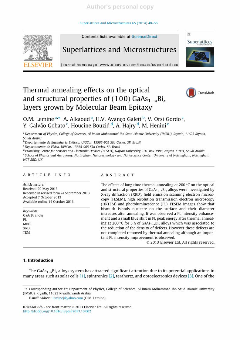
Fig. 1 shows FESEM images of substrate, GaAs1�xBix as-grown and annealed at 200 �C for 3 h. It canbe seen that the bismuth islands nucleate on the surface and these have irregular shapes (Fig. 1c).After annealing, the diameter of the island increases and their density decreases (Fig. 1e). We can con-clude that there are changes of the surface morphology of the layer due to the annealing. Similarbehavior was reported by Moussa et al. [11] for annealed GaAsBi alloys. They showed that the islandsdensity decreased with increasing the annealing temperature, and at 700 �C these islands were absent.EXDS spectra demonstrate that there is no contamination of the samples during the growth process;only Ga, As and Bi are present (Fig. 1b, d and f).
O.M. Lemine et al. / Superlattices and Microstructures 65 (2014) 48–55 49
Author's personal copy
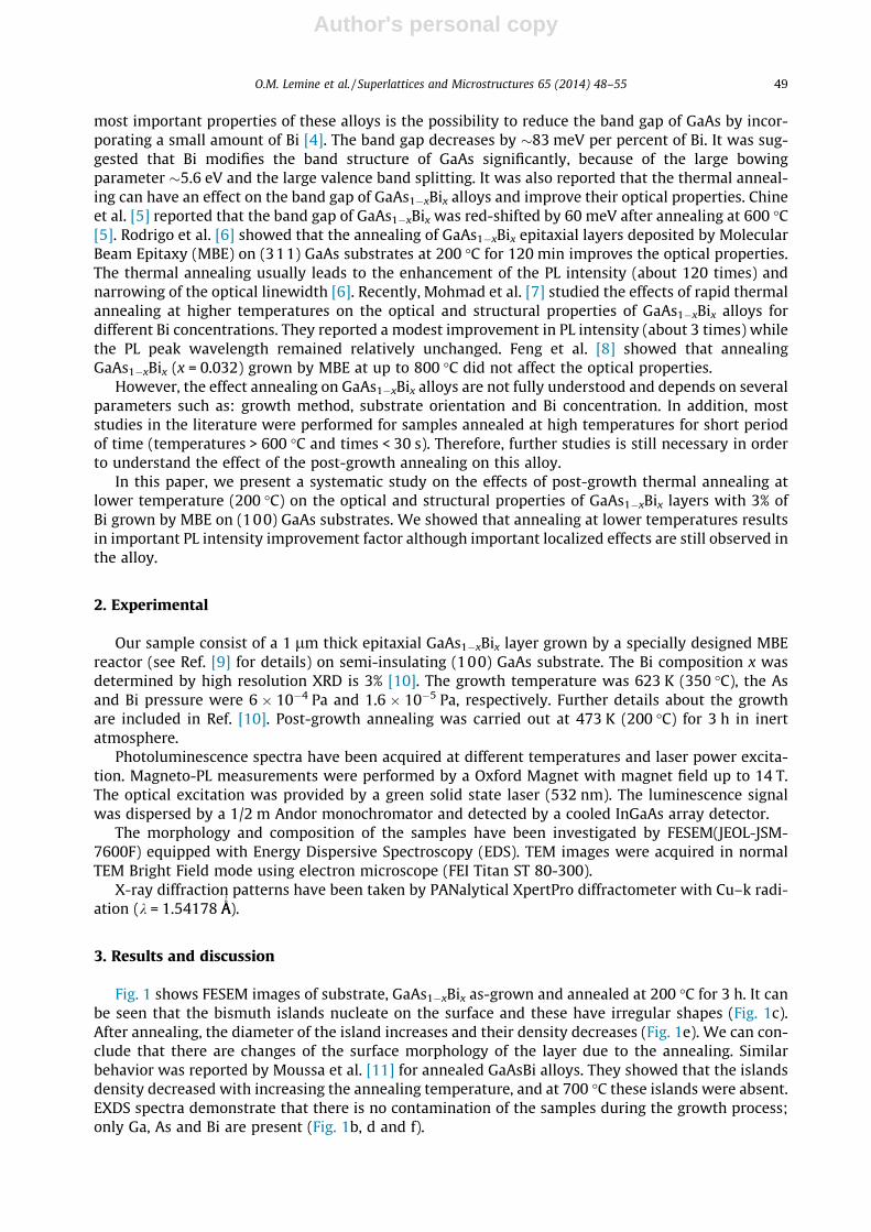
XRD patterns for the substrate, as-grown and annealed GaAs1�xBix layers at 473 K are illustrated inFig. 2. It can be seen that there are reflections peaks arising from the substrate (Fig. 2a) with GaAs CuKa1 (004) diffraction peaks, and a Cu Ka2 GaAs (004) diffraction peak and a broad peak located at thelower angles attributed to the GaAs1�xBix layers (Fig. 2b). It is also interesting to note that the reflec-tion peak intensity of the annealed sample is slightly higher than the as-grown one. Further detailsabout HRXRD measurements on these samples are included in Ref. [10].
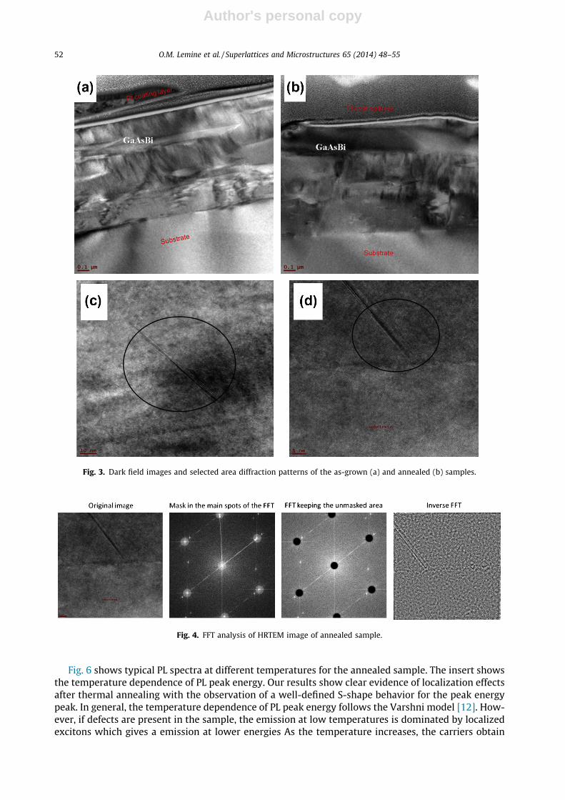
Fig. 3 shows Dark field images TEM images and selected area diffraction patterns (SAD) of theas-grown and annealed samples. It can be seen that there are several contrasts in both samples due
Fig. 1. FESEM images and EXDS spectra for substrate (a and b), as-grown GaAsBi layers (c and d) and after annealing at 473 K(e and f).
50 O.M. Lemine et al. / Superlattices and Microstructures 65 (2014) 48–55
Author's personal copy
to the structural defect and most of these defects are located in the region close to the interface be-tween GaAs and GaAsBi. For as-grown sample (Fig. 3a), the dark lines along the growth directionscould be related to threading dislocations and the different contrast in the layer could indicatechanges in the composition. We noticed also that the as-grown sample showed the presence of stack-ing fault (Fig. 3c). After annealing (Fig. 3b), there are vertical contrasts which could correspond to com-positional modulation in the layer (or ordering) or stress modulation. We can notice also that thestacking fault defects remain after annealing (Fig. 3d).
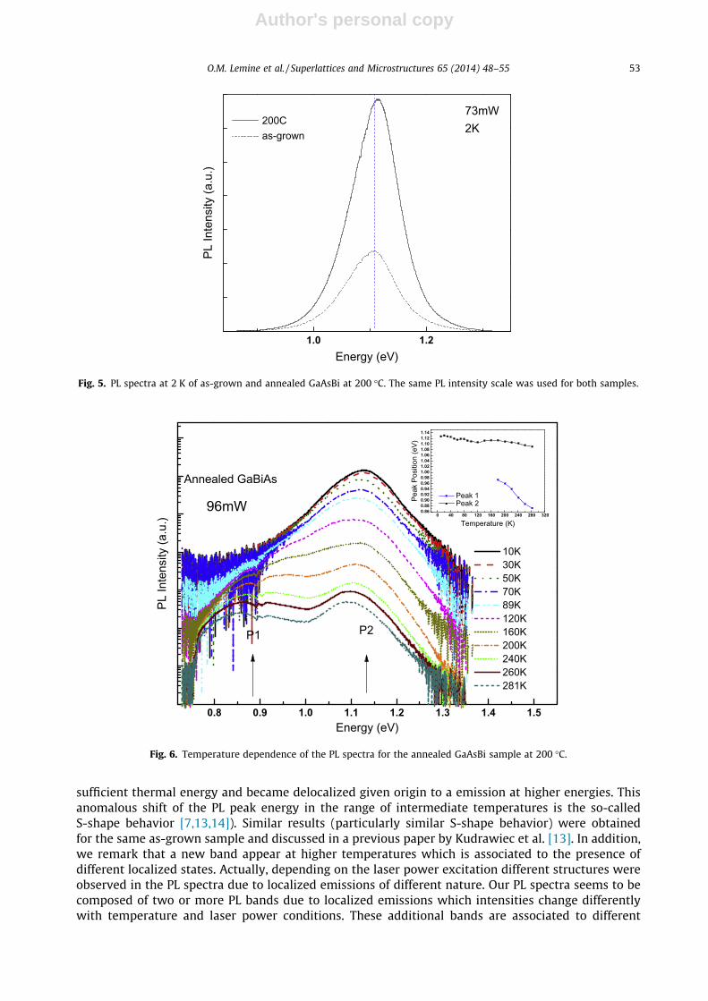
Fast fourier transform analysis (FFT) is used generally to confirm the presence of stacking fault inthe layers. An example is given in Fig. 4 for the annealed sample. By Masking the main spots of the FFTand forming the image with the unmask areas, it can be concluded that the extra spots are related tothe stacking faults in the layer.
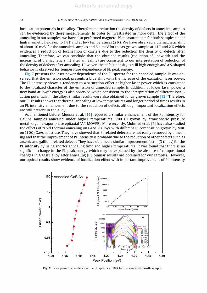
Fig. 5 shows the PL spectra at 2 K for the as-grown and annealed GaAsBi alloy at the same laserpower excitation. After annealing, the PL intensity has increased of about 2.8 times and presents asmall blue shift of about 6 meV for the PL peak energy. A small reduction of linewidth is also observedwhich indicates a slight reduction of the localized state density. Therefore the annealing at 200 �C for3 h improves the optical quality of the GaAsBi alloys with small changes of the PL peak energy. Theobserved PL intensity improvement factor is very similar to the improvement observed for GaBiAssamples that were thermal annealed at higher temperatures for low period of time such as 700 �Cand 30 s respectively [7]. In this case, the PL intensity improvement was associated to a reductionof density of defects in the alloy [7]. In order to investigate the effect of annealing in our sampleswe have also performed PL measurements as function of the temperature and laser power andmagneto-PL measurements for both samples.
Fig. 2. XRD patterns for substrate (a), and as-grown and annealed GaAs1�xBix layers at 473 K.
O.M. Lemine et al. / Superlattices and Microstructures 65 (2014) 48–55 51
Author's personal copy
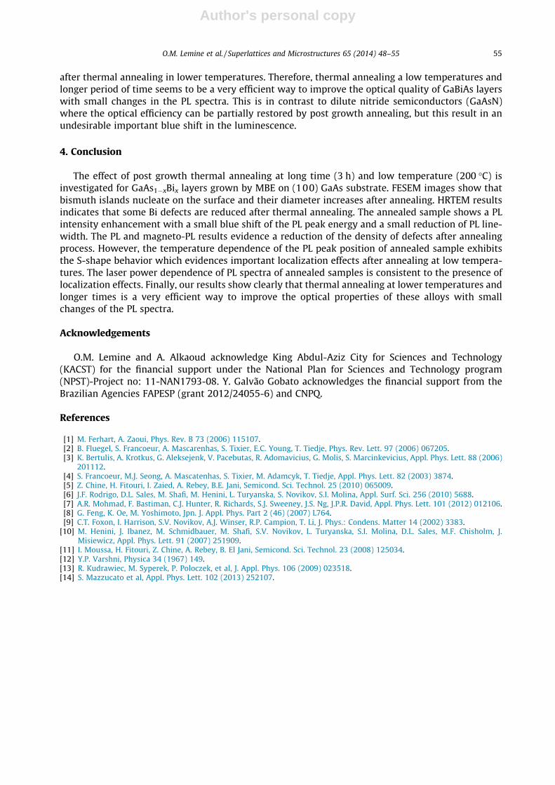
Fig. 6 shows typical PL spectra at different temperatures for the annealed sample. The insert showsthe temperature dependence of PL peak energy. Our results show clear evidence of localization effectsafter thermal annealing with the observation of a well-defined S-shape behavior for the peak energypeak. In general, the temperature dependence of PL peak energy follows the Varshni model [12]. How-ever, if defects are present in the sample, the emission at low temperatures is dominated by localizedexcitons which gives a emission at lower energies As the temperature increases, the carriers obtain
Fig. 3. Dark field images and selected area diffraction patterns of the as-grown (a) and annealed (b) samples.
Fig. 4. FFT analysis of HRTEM image of annealed sample.
52 O.M. Lemine et al. / Superlattices and Microstructures 65 (2014) 48–55
Author's personal copy
sufficient thermal energy and became delocalized given origin to a emission at higher energies. Thisanomalous shift of the PL peak energy in the range of intermediate temperatures is the so-calledS-shape behavior [7,13,14]). Similar results (particularly similar S-shape behavior) were obtainedfor the same as-grown sample and discussed in a previous paper by Kudrawiec et al. [13]. In addition,we remark that a new band appear at higher temperatures which is associated to the presence ofdifferent localized states. Actually, depending on the laser power excitation different structures wereobserved in the PL spectra due to localized emissions of different nature. Our PL spectra seems to becomposed of two or more PL bands due to localized emissions which intensities change differentlywith temperature and laser power conditions. These additional bands are associated to different
1.0 1.2
73mW2K
PL In
tens
ity (a
.u.)
Energy (eV)
200C as-grown
Fig. 5. PL spectra at 2 K of as-grown and annealed GaAsBi at 200 �C. The same PL intensity scale was used for both samples.
0.8 0.9 1.0 1.1 1.2 1.3 1.4 1.5
0 40 80 120 160 200 240 280 3200.860.880.900.920.940.960.981.001.021.041.061.081.101.121.14
Peak
Pos
ition
(eV)
Temperature (K)
Peak 1 Peak 2
10K 30K 50K 70K 89K 120K 160K 200K 240K 260K 281K
96mW
PL In
tens
ity (a
.u.)
Energy (eV)
P1 P2
Annealed GaBiAs
Fig. 6. Temperature dependence of the PL spectra for the annealed GaAsBi sample at 200 �C.
O.M. Lemine et al. / Superlattices and Microstructures 65 (2014) 48–55 53
Author's personal copy
localization potentials in the alloy. Therefore, no reduction the density of defects in annealed samplescan be evidenced by these measurements. In order to investigated in more detail the effect of theannealing in our samples, we have also performed magneto-PL measurements for both samples underhigh magnetic fields up to 14 T and at low temperatures (2 K). We have observed a diamagnetic shiftof about 10 meV for the annealed samples and 6.4 meV for the as-grown sample at 14 T and 2 K whichevidences a reduction of localization of carriers due to the reduction the density of defects afterannealing. Therefore, we can conclude that the obtained results (reduction of linewidth and theincreasing of diamagnetic shift after annealing) are consistent to our interpretation of reduction ofthe density of defects after annealing. However, the defect density is still high enough and a S-shapedbehavior is observed for temperature dependence of PL peak energy.
Fig. 7 presents the laser power dependence of the PL spectra for the annealed sample. It was ob-served that the emission peak presents a blue shift with the increase of the excitation laser power.The PL intensity shows a tendency to a saturation effect at higher laser power which is consistentto the localized character of the emission of annealed sample. In addition, at lower laser power anew band at lower energy is also observed which consistent to the interpretation of different locali-zation potentials in the alloy. Similar results were also obtained for as-grown sample [13]. Therefore,our PL results shows that thermal annealing at low temperatures and longer period of times results inan PL intensity enhancement due to the reduction of defects although important localization effectsare still present in the alloy.
As mentioned before, Moussa et al. [11] reported a similar enhancement of the PL intensity forGaBiAs samples annealed under higher temperatures (700 �C) grown by atmospheric pressuremetal–organic vapor phase epitaxial (AP-MOVPE). More recently, Mohmad et al. [7] have also studiedthe effects of rapid thermal annealing on GaAsBi alloys with different Bi composition grown by MBEon (100) GaAs substrate. They have showed that Bi related defects are not easily removed by anneal-ing and that the improvement of PL intensity is probably due to the reduction of other defects such asarsenic and gallium related defects. They have obtained a similar improvement factor (3 times) for thePL intensity by using shorter annealing time and higher temperatures. It was found that there is nosignificant change in the PL peak energy which may be explained by the absence of compositionalchanges in GaAsBi alloy after annealing [6]. Similar results are obtained for our samples. However,our optical results show evidence of localization effect with important improvement of PL intensity
1.00 1.05 1.10 1.15 1.20 1.25 1.30 1.35 1.401E-3
0.01
0.1
1
10
100
Lase
r Pow
er (m
W)
Peak Position (eV)
1
10
100
1000
10000
100000
1000000
1E7
PL In
tens
ity (a
.u.)
Energy (eV)
3.0uW 6.7uW 18.0uW 55.0uW 180.0uW 580.0uW 2.5mW 8.1mW 27.3mW 86.0mW
9K
0.8 0.9 1.0 1.1 1.2 1.3 1.4 1.5 1.6
1E-3 0.01 0.1 1 10 100
100
1000
10000
100000
1000000
Inte
grat
ed P
L In
tens
ity (a
.u.)
Laser Power (mW)
Annealed GaBiAs
Fig. 7. Laser power dependence of the PL spectra at 10 K for the annealed GaAsBi sample.
54 O.M. Lemine et al. / Superlattices and Microstructures 65 (2014) 48–55
Author's personal copy
after thermal annealing in lower temperatures. Therefore, thermal annealing a low temperatures andlonger period of time seems to be a very efficient way to improve the optical quality of GaBiAs layerswith small changes in the PL spectra. This is in contrast to dilute nitride semiconductors (GaAsN)where the optical efficiency can be partially restored by post growth annealing, but this result in anundesirable important blue shift in the luminescence.
4. Conclusion
The effect of post growth thermal annealing at long time (3 h) and low temperature (200 �C) isinvestigated for GaAs1�xBix layers grown by MBE on (100) GaAs substrate. FESEM images show thatbismuth islands nucleate on the surface and their diameter increases after annealing. HRTEM resultsindicates that some Bi defects are reduced after thermal annealing. The annealed sample shows a PLintensity enhancement with a small blue shift of the PL peak energy and a small reduction of PL line-width. The PL and magneto-PL results evidence a reduction of the density of defects after annealingprocess. However, the temperature dependence of the PL peak position of annealed sample exhibitsthe S-shape behavior which evidences important localization effects after annealing at low tempera-tures. The laser power dependence of PL spectra of annealed samples is consistent to the presence oflocalization effects. Finally, our results show clearly that thermal annealing at lower temperatures andlonger times is a very efficient way to improve the optical properties of these alloys with smallchanges of the PL spectra.
Acknowledgements
O.M. Lemine and A. Alkaoud acknowledge King Abdul-Aziz City for Sciences and Technology(KACST) for the financial support under the National Plan for Sciences and Technology program(NPST)-Project no: 11-NAN1793-08. Y. Galvão Gobato acknowledges the financial support from theBrazilian Agencies FAPESP (grant 2012/24055-6) and CNPQ.
References
[1] M. Ferhart, A. Zaoui, Phys. Rev. B 73 (2006) 115107.[2] B. Fluegel, S. Francoeur, A. Mascarenhas, S. Tixier, E.C. Young, T. Tiedje, Phys. Rev. Lett. 97 (2006) 067205.[3] K. Bertulis, A. Krotkus, G. Aleksejenk, V. Pacebutas, R. Adomavicius, G. Molis, S. Marcinkevicius, Appl. Phys. Lett. 88 (2006)
201112.[4] S. Francoeur, M.J. Seong, A. Mascatenhas, S. Tixier, M. Adamcyk, T. Tiedje, Appl. Phys. Lett. 82 (2003) 3874.[5] Z. Chine, H. Fitouri, I. Zaied, A. Rebey, B.E. Jani, Semicond. Sci. Technol. 25 (2010) 065009.[6] J.F. Rodrigo, D.L. Sales, M. Shafi, M. Henini, L. Turyanska, S. Novikov, S.I. Molina, Appl. Surf. Sci. 256 (2010) 5688.[7] A.R. Mohmad, F. Bastiman, C.J. Hunter, R. Richards, S.J. Sweeney, J.S. Ng, J.P.R. David, Appl. Phys. Lett. 101 (2012) 012106.[8] G. Feng, K. Oe, M. Yoshimoto, Jpn. J. Appl. Phys. Part 2 (46) (2007) L764.[9] C.T. Foxon, I. Harrison, S.V. Novikov, A.J. Winser, R.P. Campion, T. Li, J. Phys.: Condens. Matter 14 (2002) 3383.
[10] M. Henini, J. Ibanez, M. Schmidbauer, M. Shafi, S.V. Novikov, L. Turyanska, S.I. Molina, D.L. Sales, M.F. Chisholm, J.Misiewicz, Appl. Phys. Lett. 91 (2007) 251909.
[11] I. Moussa, H. Fitouri, Z. Chine, A. Rebey, B. El Jani, Semicond. Sci. Technol. 23 (2008) 125034.[12] Y.P. Varshni, Physica 34 (1967) 149.[13] R. Kudrawiec, M. Syperek, P. Poloczek, et al, J. Appl. Phys. 106 (2009) 023518.[14] S. Mazzucato et al, Appl. Phys. Lett. 102 (2013) 252107.
O.M. Lemine et al. / Superlattices and Microstructures 65 (2014) 48–55 55