Role of fibre properties in colour non-uniformity of dyed fabrics
Upload
independentCategory
view
5download
0
Journal of ELECTRONIC MATERIALS, Vol. 34, No. 6, 2005 Special Issue Paper
779
Lateral Uniformity in HgCdTe Layers Grown by MolecularBeam Epitaxy
BRETT Z. NOSHO,1,3 JOHN A. ROTH,1 JOHN E. JENSEN,1 and LE PHAM2
1.—HRL Laboratories, LLC, Malibu, CA 90265. 2.—Raytheon Vision Systems, Goleta, CA 93117.3.—E-mail: [email protected]
The fabrication of high-quality focal plane arrays from HgCdTe layers grownby molecular beam epitaxy (MBE) requires a high degree of lateral uniformityin material properties such as the alloy composition, doping concentration,and defect density. While it is well known that MBE source flux nonuniformitycan lead to radial compositional variation for rotating substrates, we have alsofound that composition can be affected significantly by lateral variations insubstrate temperature during growth. In diagnostic experiments, we system-atically varied the substrate temperature during MBE and quantified the dependence of HgCdTe alloy composition on substrate temperature. Based onthese results, we developed a methodology to quickly and nondestructivelycharacterize MBE-grown layers using postgrowth spatial mapping of the cut-off wavelength from the Fourier transform infrared (FTIR) transmission at300 K, and we were able to obtain a quantitative relationship between themeasured spatial variations in cutoff and the substrate temperature lateraldistribution during growth. We refined this methodology by more directly inferring the substrate temperature distribution from secondary ion massspectroscopy (SIMS) measurements of the As concentration across a wafer,using the fact that the As incorporation rate in MBE-grown p-type layers ishighly sensitive to substrate temperature. Combining this multiple-pointSIMS analysis with FTIR spatial mapping, we demonstrate how the relativecontributions from flux nonuniformity and temperature variations on the lateral composition uniformity can be separated. This capability to accuratelymap the lateral variations in the substrate temperature has been valuable inoptimizing the mounting and bonding of large substrates for MBE growth, andcan also be valuable for other aspects of MBE process development.
Key words: Molecular beam epitaxy (MBE), HgCdTe, infrared, arsenic doping
(Received October 7, 2004; accepted January 17, 2005)
INTRODUCTION
The growth of HgCdTe by molecular beam epitaxy(MBE) has emerged as a leading technology in the development of advanced infrared focal planearrays. The fabrication of high-quality focal planearrays from MBE-grown HgCdTe layers requires ahigh degree of control of material properties such asthe alloy composition, doping concentration, and defect density. Historically, the focus has been onachieving run-to-run consistency, which has largelybeen addressed by the integration of sensors and
automated feedback to monitor and regulate the composition by spectroscopic ellipsometry (SE)throughout the growth of the epilayers.1 As MBEgrowth of HgCdTe heterostructures continues tomature, it has become evident that in addition toimproving the wafer yield with higher performancespecifications, the future of MBE-grown detectorsrequires the transition toward a manufacturingtechnology that can also increase the yield of focalplane arrays per wafer by growing laterally uniformHgCdTe layers on larger substrates.
A clear requirement of this objective is achieving ahigh degree of composition uniformity to provideconsistent material properties across the entire
JEM-1324-S18 6/7/05 8:10 AM Page 779
780 Nosho, Roth, Jensen, and Pham
wafer. For solid-source MBE, it is well known that aradial variation in composition may exist even whendepositing on rotating substrates. The extent of thiscontribution depends on the design of the cell geome-try, including the level of source material depletionin the effusion cells. While MBE growth on rotatingsubstrates is generally regarded to yield epitaxiallayers with highly uniform composition, for infrareddetectors, the required uniformity is greater than formost other applications. We note that a change ofonly 0.001 in the CdTe mole fraction (x value) of aHg1–xCdxTe layer with an x value of 0.224 (i.e., achange of only 0.5%) will shift the 300 K Fouriertransform infrared (FTIR) transmission cutoff wave-length by �0.05 µm, which projects to a shift in the78 K cutoff wavelength of �0.15 µm. A second poten-tial cause of composition nonuniformity is lateralvariation in the substrate temperature during MBEgrowth. Although the exact growth mechanisms ofHgCdTe are not well understood, there have beensome attempts to address the basic thermodynamicprinciples.2–5 Generally, the discussions have beendirected toward the formation of defects, however,since substrate temperature is intimately related to the surface Hg atom density and the dissociationkinetics of Te2, it is easy to envision how substratetemperature variations would also impact the alloycomposition. Not only will variations in the sub-strate temperature affect composition, but can alsoinfluence the size and density of void defects, as wellas the incorporation of arsenic as a p-type dopant.2,3
In the following sections, we present the results ofexperiments to determine the causes of composi-tional nonuniformity during the growth of HgCdTeon large substrates up to 5 � 5 cm in size. First, wedetermine quantitatively the effect of substrate tem-perature on x value during the growth of HgCdTe,and show how the variation of As in an in situ-dopedp-type layer can be used to infer the local substratetemperature, and the corresponding local x value. By combining these two results, the component of x-value variation due to flux nonuniformities is sepa-rated from the total x-value variation across thewafer. Knowledge of the flux component then allowsthe substrate temperature variation to be quicklyand nondestructively computed for subsequent runsdirectly from a map of FTIR cutoff. This temperaturemapping capability can be very useful in under-standing the influence of different substrate mount-ing schemes on the uniformity of MBE growth onlarge substrates.
EXPERIMENT
The HgCdTe epitaxial layers in this study weregrown on commercially available CdZnTe (211)Bsubstrates in a VG Semicon (East Grinstead, WestSussex, UK) V80H MBE system equipped with com-pound CdTe and elemental Hg and Te sources, in addition to In and As dopant cells. This system wasdesigned to handle substrates up to 3 in. in diame-ter; however, we have used it mainly to grow on
rectangular and square substrates ranging in sizeup to 5 cm � 5 cm. Prior to growth, the CdZnTe sub-strates were degreased with solvents, etched in a 1% Br-methanol solution, and then rinsed withmethanol and deionized water. Following the clean-ing process, substrates were bonded onto the sub-strate mounting block using a colloidal graphitepaste and then transferred into the vacuum system.During the epitaxial growth of Hg1–xCdxTe layers,the alloy composition, or x value, was regulatedusing SE, while the substrate temperature was regu-lated using absorption edge spectroscopy (ABES) ona witness sample bonded directly to the opposite sideof the growth block.1 It should be noted that eventhough the use of SE guarantees that the x value atthe center of the wafer will be very close to the targetvalue, the x value elsewhere on the wafer is free torespond to the local substrate temperature and fluxvalues if they differ from those at the center.
Postgrowth FTIR analysis of the HgCdTe layerswas done at room temperature using a Thermo-Nicolet (Waltham, MA) FTIR spectrometer that wasmodified with an automated stage to allow for full-wafer spatial mapping. For mapping, a series of indi-vidual transmission spectra are typically recorded ata grid of points 1–3 mm apart that cover the entirewafer. For the present work, the cutoff wavelength isdefined to be the wavelength at which the transmis-sion reaches 50% of its maximum value, where thelatter is taken to be the average transmission valueover the wavelength region where the sample istransparent. All SIMS analyses were performed atCharles Evans and Associates.
RESULTS AND DISCUSSIONFor this study, we were primarily interested in
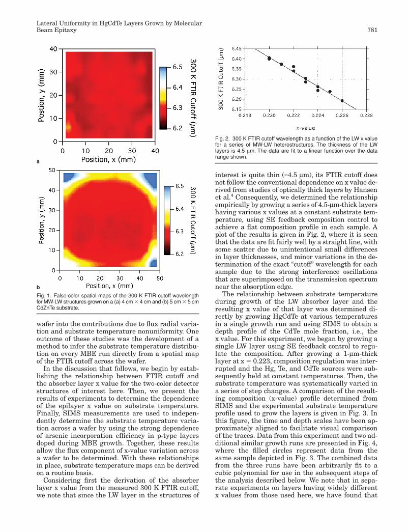
n-p-n two-color detectors grown on large CdZnTesubstrates. The two-color structure consists of a 10 µm-thick n-type mid-wave (MW) layer, with a 4 µm-thick p-type layer and a 4.5 µm-thick n-typelong-wave (LW) layer grown on top of the MW layer.Indium and arsenic are used as the n-type and p-type dopants, respectively. To illustrate the diffi-culties that can arise in achieving lateral composi-tional uniformity as the substrate size increases,false-color spatial maps of the 300 K FTIR cutoffwavelength are shown in Fig. 1 for two-color struc-tures grown on 4 cm � 4 cm and 5 cm � 5 cm sub-strates. The cutoff wavelength, and correspondinglythe HgCdTe composition, or x value is fairly uniformacross the majority of both samples. However, toward the corners and edges of the 5 cm � 5 cmsubstrate, the cutoff wavelength increases, reflect-ing a reduced x value in these regions. The maingoal of the work reported here was to determine theprinciple causes of this roll-off in x value in order todetermine if the uniformity can be improvedthrough changes in source configuration or sub-strate mounting. This issue was approachedthrough a series of experiments designed to sepa-rate the total measured variation in x value across a
JEM-1324-S18 6/7/05 8:10 AM Page 780
Lateral Uniformity in HgCdTe Layers Grown by MolecularBeam Epitaxy 781
wafer into the contributions due to flux radial varia-tion and substrate temperature nonuniformity. Oneoutcome of these studies was the development of amethod to infer the substrate temperature distribu-tion on every MBE run directly from a spatial mapof the FTIR cutoff across the wafer.
In the discussion that follows, we begin by estab-lishing the relationship between FTIR cutoff andthe absorber layer x value for the two-color detectorstructures of interest here. Then, we present the results of experiments to determine the dependenceof the epilayer x value on substrate temperature. Finally, SIMS measurements are used to indepen-dently determine the substrate temperature varia-tion across a wafer by using the strong dependenceof arsenic incorporation efficiency in p-type layersdoped during MBE growth. Together, these resultsallow the flux component of x-value variation acrossa wafer to be determined. With these relationshipsin place, substrate temperature maps can be derivedon a routine basis.
Considering first the derivation of the absorberlayer x value from the measured 300 K FTIR cutoff,we note that since the LW layer in the structures of
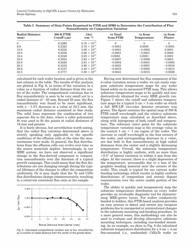
interest is quite thin (≈4.5 µm), its FTIR cutoff doesnot follow the conventional dependence on x value de-rived from studies of optically thick layers by Hansenet al.4 Consequently, we determined the relationshipempirically by growing a series of 4.5-µm-thick layershaving various x values at a constant substrate tem-perature, using SE feedback composition control toachieve a flat composition profile in each sample. Aplot of the results is given in Fig. 2, where it is seenthat the data are fit fairly well by a straight line, withsome scatter due to unintentional small differencesin layer thicknesses, and minor variations in the de-termination of the exact “cutoff” wavelength for eachsample due to the strong interference oscillationsthat are superimposed on the transmission spectrumnear the absorption edge.
The relationship between substrate temperatureduring growth of the LW absorber layer and the resulting x value of that layer was determined di-rectly by growing HgCdTe at various temperaturesin a single growth run and using SIMS to obtain adepth profile of the CdTe mole fraction, i.e., the x value. For this experiment, we began by growing asingle LW layer using SE feedback control to regu-late the composition. After growing a 1-µm-thicklayer at x � 0.223, composition regulation was inter-rupted and the Hg, Te, and CdTe sources were sub-sequently held at constant temperatures. Then, thesubstrate temperature was systematically varied ina series of step changes. A comparison of the result-ing composition (x-value) profile determined fromSIMS and the experimental substrate temperatureprofile used to grow the layers is given in Fig. 3. Inthis figure, the time and depth scales have been ap-proximately aligned to facilitate visual comparisonof the traces. Data from this experiment and two ad-ditional similar growth runs are presented in Fig. 4,where the filled circles represent data from thesame sample depicted in Fig. 3. The combined datafrom the three runs have been arbitrarily fit to acubic polynomial for use in the subsequent steps ofthe analysis described below. We note that in sepa-rate experiments on layers having widely different x values from those used here, we have found that
a
b
Fig. 1. False-color spatial maps of the 300 K FTIR cutoff wavelengthfor MW-LW structures grown on a (a) 4 cm � 4 cm and (b) 5 cm � 5 cmCdZnTe substrate.
Fig. 2. 300 K FTIR cutoff wavelength as a function of the LW x valuefor a series of MW-LW heterostructures. The thickness of the LW layers is 4.5 µm. The data are fit to a linear function over the datarange shown.
JEM-1324-S18 6/7/05 8:10 AM Page 781

782 Nosho, Roth, Jensen, and Pham
the exact relationship can vary somewhat from thatshown in Fig. 4. However, the general shape of thedependence is preserved, and a simple scale factorcan be used to generalize the results to x valuesspanning the full LW and MW composition range.
If there were no spatial variation in the incidentfluxes over the area of the substrate, the relation-ship shown in Fig. 4, together with the cutoff to x-value conversion from Fig. 2, would be sufficient toinfer the lateral variation in substrate temperaturedirectly from a spatial map of FTIR cutoff. However,on larger substrates, the flux contribution is not insignificant. In this case, one needs a means to determine the flux contribution independently. Todo this, we used the difference between the x-valuedistribution calculated from FTIR cutoff and the x-value distribution estimated from a multiple-pointSIMS analysis of the arsenic concentration in a
p-type layer, based on knowledge of the temperaturedependence of As incorporation and the previouslyderived relation between substrate temperature andx value. The residual difference between these twox-value distributions is in effect the component dueto flux nonuniformity alone. In Fig. 5, we show thedependence of As on substrate temperature deter-mined empirically by growing a p-type arsenic-doped layer and varying the substrate temperaturein steps during the growth, while holding the Assource at a constant temperature. The substratetemperature steps were known quite accurately be-cause the substrate temperature was monitored andfeedback-controlled throughout the growth usingABES. The very strong dependence of As incorpora-tion on substrate temperature allows the SIMS Asconcentration at each point on a sample to be used tocalculate the substrate temperature to better than1°, even with the �10% precision for As determina-tion by SIMS, as quoted by Charles Evans and Asso-ciates (Sunnyvale, CA). By using the relationship between substrate temperature and x value given inFig. 4, the variations in x value can then be derivedto a correspondingly high degree of precision.
The procedure just described was put into practiceby using a n-p-n two-color structure grown on a 5 � 5 cm substrate. After obtaining an FTIR map ofthe cutoff, the arsenic concentration was deter-mined by SIMS at ten locations on the wafer span-ning a range of radial distances from the center outto a radius of nearly 33 mm. The results of thisanalysis of these data are shown in Table I. For eachlocation on the wafer where SIMS was done, the dif-ference in the local FTIR cutoff relative to the valueat the center of the wafer was converted to an x-value difference by using the relationship shownin Fig. 4. Additionally, the local As concentrationwas used to calculate at each location the tempera-ture difference from the center of the wafer, usingthe relationship from Fig. 5, and the amount of x-value difference that would be caused by this temperature difference alone was computed fromthe relationship in Fig. 4. Finally, by subtracting thetemperature-derived component of the x-value difference from the total difference measured byFTIR, the net effect due to flux variation has been
Fig. 3. A comparison of (a) the logged substrate growth temperatureand (b) the x value as measured by SIMS analysis for a samplewhere the growth temperature was systematically varied to calibratehow changes in growth temperature affect the layer composition.
a
b
Fig. 4. A plot of the change in x value due to changes in substratetemperature for three different calibration samples. The filled circlesrepresent the data taken from the sample in Fig. 2. The data are fit toa cubic polynomial function.
Fig. 5. Arsenic concentration measured from SIMS as a function ofthe substrate growth temperature.
JEM-1324-S18 6/7/05 8:10 AM Page 782
Lateral Uniformity in HgCdTe Layers Grown by MolecularBeam Epitaxy 783
calculated for each wafer location and is given in thelast column in the table. The results of this analysisare plotted in Fig. 6, in terms of the variation in xvalue as a function of radial distance from the cen-ter of the wafer. The compositional variation due toflux nonuniformity is seen to be very small out to a radial distance of �25 mm. Beyond 25 mm, the fluxnonuniformity was found to be more significant,with a �1.3% decrease in x value at 32.5 mm, themaximum radial distance examined in this study.The solid lines represent the combination of twoseparate fits to the data, where a cubic polynomialfit was used to fit the points at radial distances of 18 mm and greater.
It is fairly obvious, but nevertheless worth noting,that the radial flux variation determined above isstrictly speaking only applicable to the specific conditions of the effusion cells at the time the mea-surements were made. In general, the flux distribu-tions from the effusion cells can evolve over time asthe source materials deplete. Interestingly, in ourMBE system, we have not observed a significantchange in the flux-derived component to composi-tion nonuniformity over the duration of a typicalgrowth campaign. This could mean that the flux dis-tributions are not changing enough during the typi-cal lifetimes of the charges to affect the compositionuniformity. Or it may imply that the Te and CdTeflux distributions change commensurately, resultingin a relatively consistent flux ratio at the sample.
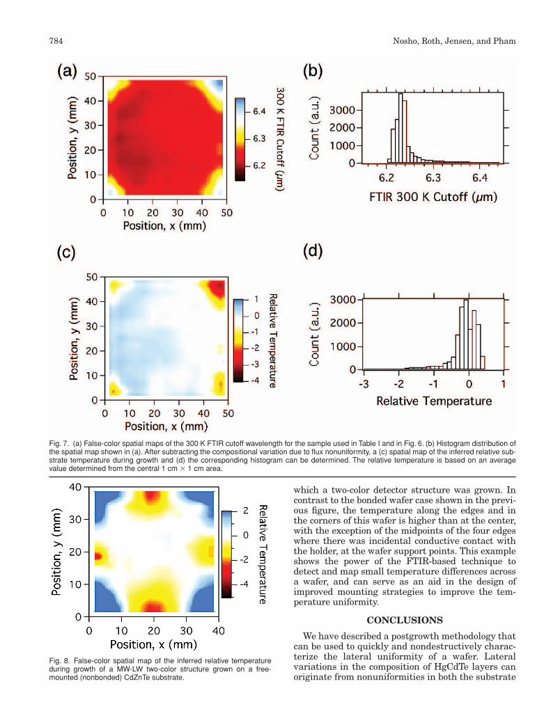
Having now determined the flux component of thex-value variation across a wafer, we can easily com-pute substrate temperature maps for any waferbased solely on its measured FTIR map. This allowssubstrate temperature maps to be quickly and non-destructively obtained for every MBE growth run.Figure 7 shows the cutoff and substrate tempera-ture maps for a typical 5 cm � 5 cm wafer on whicha full MW-LW two-color detector structure wasgrown. The figure contains the spatial map of 300 KFTIR cutoff wavelength and the relative substratetemperature map calculated as described above,along with histograms of both cutoff and tempera-ture. The reference (zero) point for the substratetemperature variation map is the average value inthe central 1 cm � 1 cm region of the wafer. The increase in cutoff wavelength in the four corners ofthe wafer, and corresponding decrease in x value,are due both to flux nonuniformity at high radialdistances from the center and a slightly decreasingtemperature. Overall, the substrate temperaturedistribution is highly uniform, with no more than�0.5° of lateral variation to within 2 mm from theedges. At the corners, there is a slight depression ofthe temperature, presumably due to a loss of thegraphite bonding material near the corners of thewafer. This result is typical for our current waferbonding technology, which results in highly uniformdistributions of composition and arsenic dopant concentration over the entire usable portion of thewafer.
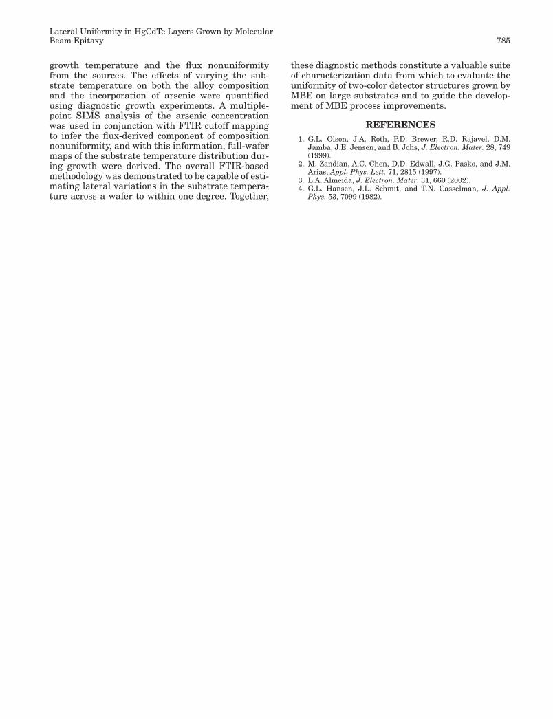
The ability to quickly and inexpensively map thesubstrate temperature distribution on every waferprovides an invaluable diagnostic tool for character-izing MBE-grown layers. For wafers conductivelybonded to holders, this FTIR-based analysis providesan easy process to detect and correct any incipientproblems due to unexpected or unintentional changesin the substrate mounting and bonding procedure. Ina more general sense, this methodology can also beused to evaluate and develop alternative substratemounting techniques, including non-bonded mount-ing. As an example, we show in Fig. 8 the calculatedsubstrate temperature distribution for a 4 cm � 4 cmfree-mounted (i.e., nonbonded) CdZnTe wafer on
Table I. Summary of Data Points Examined by FTIR and SIMS to Determine the Contribution of FluxNonuniformity on Composition Variation
Radial Distance 300 K FTIR [As] ∆x Total ∆x from ∆x from(mm) Cutoff (µm) (cm�3) from FTIR Temperature Fluxes
0 6.2290 2.70 � 1017 0 0 09.9 6.2323 2.78 � 1017 �0.0001 0.0000 �0.000113.0 6.2330 3.00 � 1017 �0.0001 �0.0002 0.000118.0 6.2336 2.86 � 1017 �0.0001 �0.0001 0.000018.4 6.2249 2.63 � 1017 0.0002 0.0001 0.000123.0 6.2504 3.82 � 1017 �0.0007 �0.0006 0.000124.0 6.2428 2.81 � 1017 �0.0004 �0.0001 �0.000328.3 6.3219 3.95 � 1017 �0.0023 �0.0007 �0.001628.6 6.3127 3.48 � 1017 �0.0018 �0.0005 �0.001332.5 6.3777 5.88 � 1017 �0.0041 �0.0015 �0.0026
Fig. 6. Calculated compositional variation due to flux nonuniformityas a function of radial distance from the center of the growth block.
JEM-1324-S18 6/7/05 8:10 AM Page 783
784 Nosho, Roth, Jensen, and Pham
which a two-color detector structure was grown. Incontrast to the bonded wafer case shown in the previ-ous figure, the temperature along the edges and inthe corners of this wafer is higher than at the center,with the exception of the midpoints of the four edgeswhere there was incidental conductive contact withthe holder, at the wafer support points. This exampleshows the power of the FTIR-based technique to detect and map small temperature differences acrossa wafer, and can serve as an aid in the design of improved mounting strategies to improve the tem-perature uniformity.
CONCLUSIONS
We have described a postgrowth methodology thatcan be used to quickly and nondestructively charac-terize the lateral uniformity of a wafer. Lateral variations in the composition of HgCdTe layers canoriginate from nonuniformities in both the substrate
Fig. 7. (a) False-color spatial maps of the 300 K FTIR cutoff wavelength for the sample used in Table I and in Fig. 6. (b) Histogram distribution ofthe spatial map shown in (a). After subtracting the compositional variation due to flux nonuniformity, a (c) spatial map of the inferred relative sub-strate temperature during growth and (d) the corresponding histogram can be determined. The relative temperature is based on an averagevalue determined from the central 1 cm � 1 cm area.
Fig. 8. False-color spatial map of the inferred relative temperatureduring growth of a MW-LW two-color structure grown on a free-mounted (nonbonded) CdZnTe substrate.
JEM-1324-S18 6/7/05 8:10 AM Page 784
Lateral Uniformity in HgCdTe Layers Grown by MolecularBeam Epitaxy 785
these diagnostic methods constitute a valuable suiteof characterization data from which to evaluate theuniformity of two-color detector structures grown byMBE on large substrates and to guide the develop-ment of MBE process improvements.
REFERENCES1. G.L. Olson, J.A. Roth, P.D. Brewer, R.D. Rajavel, D.M.
Jamba, J.E. Jensen, and B. Johs, J. Electron. Mater. 28, 749(1999).
2. M. Zandian, A.C. Chen, D.D. Edwall, J.G. Pasko, and J.M.Arias, Appl. Phys. Lett. 71, 2815 (1997).
3. L.A. Almeida, J. Electron. Mater. 31, 660 (2002).4. G.L. Hansen, J.L. Schmit, and T.N. Casselman, J. Appl.
Phys. 53, 7099 (1982).
growth temperature and the flux nonuniformityfrom the sources. The effects of varying the sub-strate temperature on both the alloy compositionand the incorporation of arsenic were quantifiedusing diagnostic growth experiments. A multiple-point SIMS analysis of the arsenic concentrationwas used in conjunction with FTIR cutoff mappingto infer the flux-derived component of compositionnonuniformity, and with this information, full-wafermaps of the substrate temperature distribution dur-ing growth were derived. The overall FTIR-basedmethodology was demonstrated to be capable of esti-mating lateral variations in the substrate tempera-ture across a wafer to within one degree. Together,
JEM-1324-S18 6/7/05 8:10 AM Page 785
Copyright © 2022 FDOKUMEN