Structural and optical characterization of SixGe1−x−ySny alloys grown by molecular beam epitaxy
12
Structural and Optical Characterization of Silicon Nanocrystals Obtained by Ion Implantation S. N. M. Mestanza 1 , G. O. Dias 1 , J. E. C. Queiroz 1 , I. Doi 1 and J. W. Swart 1 E. Rodriguez 2 , A. A. R. Neves 2 , H. Martinho 2 1 Centro de Componentes Semicondutores CCS/FEEC-UNICAMP, CP6165, 13083-970 Campinas, SP, Brazil 2 Instituto de Física Gleb Wataghin IFGW/DEQ-UNICAMP, CP6165, 13083-970 Campinas, SP, Brazil e-mail: [email protected] Abstract Photoluminescence (PL) was used to investigate the luminescence mechanism in Si nanocrystals. Si ions were implanted in SiO 2 films at 100 keV to a dose of 5x10 16 / cm 2 . An intense photoluminescence band in (1.2-1.6) eV was observed after implanted films were annealed at 1000 o C in nitrogen. Deconvolution of photoluminescence suggests that others recombination centers possibly are present into the samples. Red PL band (1.5 eV) was attributed to emission from Si nanocrystals because gaussian peak in the 1.5 eV increase continuously with annealing temperature became narrower. Raman spectra for all samples show a band approximately at 521 cm -1 , related to typical nanocrystalline silicon. From the X-ray diffraction (XRD) results the clusters are shown crystalline and with plane orientation (311). Scanning electron microscopy (SEM) and atomic force microscopy (AFM) images showed the presence of Si nanocrystals with diameter ~ 10 nm on etched annealed samples. Keywords: Clusters, silicon, ion implantation, Raman spectroscopy, silicon oxide. 1
Transcript of Structural and optical characterization of SixGe1−x−ySny alloys grown by molecular beam epitaxy

Structural and Optical Characterization of Silicon Nanocrystals
Obtained by Ion Implantation
S. N. M. Mestanza1, G. O. Dias1, J. E. C. Queiroz1, I. Doi1 and J. W. Swart1
E. Rodriguez2, A. A. R. Neves2, H. Martinho2
1Centro de Componentes Semicondutores CCS/FEEC-UNICAMP, CP6165, 13083-970 Campinas, SP, Brazil
2Instituto de Física Gleb Wataghin IFGW/DEQ-UNICAMP, CP6165, 13083-970 Campinas, SP, Brazil
e-mail: [email protected]
Abstract
Photoluminescence (PL) was used to investigate the luminescence mechanism in Si
nanocrystals. Si ions were implanted in SiO2 films at 100 keV to a dose of 5x10¹⁶ / cm2. An
intense photoluminescence band in (1.2-1.6) eV was observed after implanted films were
annealed at 1000oC in nitrogen. Deconvolution of photoluminescence suggests that others
recombination centers possibly are present into the samples. Red PL band (1.5 eV) was
attributed to emission from Si nanocrystals because gaussian peak in the 1.5 eV increase
continuously with annealing temperature became narrower. Raman spectra for all samples
show a band approximately at 521 cm-1, related to typical nanocrystalline silicon. From the
X-ray diffraction (XRD) results the clusters are shown crystalline and with plane
orientation (311). Scanning electron microscopy (SEM) and atomic force microscopy
(AFM) images showed the presence of Si nanocrystals with diameter ~ 10 nm on etched
annealed samples.
Keywords: Clusters, silicon, ion implantation, Raman spectroscopy, silicon oxide.
1

I - Introduction
In spite of high efficiency emitter devices can be obtained from III-V
semiconductor compounds; its integration in the current Si planar technology is very
complex and often ineffective. On the other hand silicon is a very poor emitter due to its
indirect band gap. However, in nanocrystal form (Si-nano), silicon properties change
drastically presenting a direct band gap with emission in the wavelength range of [600-
1000] nm, depending on the nanocrystal size distribution. Samples obtained by
implantation of silicon into silicon oxide matrix present strong PL in the range cited above
[1]. These silicon nanoclusters have been studied along several years as a promised
structure to be applicable in photonic technology. Many techniques have been used to
produce silicon nanoparticles into silicon oxide, however the most advantageous technique
is the ion implantation, because, among other advantages, presents the possibility of
controls the depth of distribution of ions.
Mechanism of optical gain into these nanocrystalline structures remains not well
explained. Some works report the decreasing of photoluminescence intensity after
annealing [2] and others report just the contrary, i.e., the increasing of determined
photoluminescence band intensities after annealing time, up to the saturation [3]. Still isn't
well understood what is the real contribution of the nanoclusters on the new observed
luminescence. Ion implantation technique itself causes defects that may be related to this
luminescence [4]. Many experiments have been carried out in order to clarify the origin of
photoluminescence bands in structures created by ion implantation of Si into SiO2 [4].
2

Silicon is a very desirable candidate for photonic technology, because it is found in
abundance in all the Earth and the technology of silicon is well known and developed,
which result in low cost processes. Indeed, as the technology related to microelectronics is,
nowadays, based in 98% on silicon, development of optoelectronics technology also based
in silicon is of great interest, because this could lead to create a bridge between
microelectronics and optoelectronics.
It is well known that photoluminescence bands in structures created by implantation
of Si into SiO2 are dependent on ion dose (concentration of ion implanted), annealing time
and annealing temperature.
Thermal silicon oxides with ~ 300 nm, were grown on (100) p-Si wafers. 28Si+
implantation was performed with energies of 100 keV. The implantation energies were
chosen from Monte Carlo simulation, using the TRIM code. Conventional PL spectra were
obtained at room temperature, showing a broad luminescence band in the red region for all
the samples. We have studied the behavior of PL emission peak and full width at half
maximum (FWHM) with the annealing time. We have estimated the size of nanocrystals by
PL and Raman spectroscopy analysis.
II – Experimental
Our samples were prepared by implantation of Si into thermal oxidized p-doped
(100) silicon wafers. The p-doped Si substrate had a thickness of 393 µm, V/I ratio of
3
Ω± )36.085.25( and the measured resistivity was 4.60 Ωcm, with a dopant concentration
of 3.0x1015 cm-3. These silicon wafers were cleaned following the standard RCA cleaning
process. After, the thermal oxidation was carried out in a conventional furnace at
temperature of 1000oC.
The thickness (measured by 632.8 nm He/Ne laser Rudolph Ellipsometer, model
AUTO EL) of grown oxide was 310 nm. The dose of implanted silicon was 5.0x1016 cm-2
at energy of 100 keV. Annealing was realized at 1000oC on these silicon-implanted samples
at times of 1h, 2h and 3h.
The PL spectra were obtained by an argon laser excitation source, with excitation
lines of 488 nm and 514 nm, at powers between mW)5100( ± , at room temperature. The
PL measurements were performed using a MG252 SPECTRAL ENERGY monochromator
with a blaze grid of 1 micra of 590 lines/mm. The detector used was a PIN Si photodiode
model 818-BB-40 of the Newport.
Raman spectroscopy was carried out to investigate the possible formation of silicon
nanocrystals into SiO2 matrix. We aim to observe emission about 521cm-1, typical of
monocrystaline silicon. The excitation light source at 488 nm was emitted from a Spectra
Physics argon laser with an incident power of around 10 mW.
For the morphological analysis we use a Field Emission Gun Microscope (FEG)
JSM 6330F Jeol. Micrographs were also obtained with a Topometrix AFM Microscope,
model DISCOVERER, by non-contact technique.
4
In order to observe the formation of clusters inside the oxide we carried out an
etching with buffer of HF to discover the clusters formed. The ratio of corrosion was nearly
1000 Å/min. We did 1.20 minutes corrosion, and after the oxide thickness was measured,
which result approximately 150 nm.
III - Analysis and Discussion
Fig. 1 shows time evolution of the photoluminescence spectra of the three annealed
samples studied (B, C, D) at 1000oC for several hours. It’s clear from the figure that the
photoluminescence intensity and annealing time are directly dependent, increasing
altogether. It’s also clear that peak energies of the luminescence spectra are independent of
the annealing time in all the samples. These results are in accordance to those reported in
literature [3]. The fact that not well defined PL peak was observed we attribute basically to
factors related with stequiometric composition of the SiO2 matrix. In one first
approximation we could say that in fig. 1 the PL peak stayed in the same position, so it is
related with the same energy band. This fact could be showing that clusters size is not
increasing with the increase of the annealing time. Indeed the clusters are always increasing
with the annealing time. However, we observe an apparently unmovable energy peak of PL
and we suppose that it is basically due to emission from a new generation of clusters,
originating from silicon dispersed in SiO2 matrix. Another curious fact is that spectra show
a broad PL band, centered between 1.4-1.5 eV, which seems a superposition of different
band contributions.
5

To better understand these results, we carried out gaussian adjusts for each PL
spectrum (fig. 2). We can observe from these adjusts that each spectrum may be very well
fit by three contributions (gaussians α, β, γ) with the following characteristics: for all
instant α, β and γ show the same energy peak; the intensity for β and γ contributions stay
constant. Only for α contribution one observe a continuous increasing in intensity, a
narrowing of bandwidth with annealing time and independence of energy peak position
(from the literature, this is a typical behavior of a nanocrystal that satisfy the quantum
confinement model). These results lead us think that β e γ emissions can be attributed to
recombination processes in cluster-Si/SiO2 interface or yet to defects in SiO2 matrix.
Concerning the theorist-experimental curves of diameter vs. Energy reported [5],
[6], [7], we have estimated the diameter of our nanocrystals utilizing for this the peak of
contribution α in fig. 2. The peak of this curve (α) is localized in approximately 1.5eV and
clusters associated with this peak would have ~ 9nm in size.
Raman spectroscopy is an efficient technique to evaluate quantitatively
measurements of stress, presence of nanocrystals and homogeneity. Si crystals have typical
characteristic of strength emission and narrow band at 521cm-1, which corresponds to
transverse acoustic mode in first order. However in the case of amorphous silicon, the lack
of order induce to modifications in the vibrational density of states and in this case the
Raman spectrum is characterized for two faint and broad bands at 150cm-1 and 480cm-1.
6

We measured the Raman spectra of sample B and C (3 and 2 hours annealing,
respectively). The results are shown in the fig.3. A few observations can be easily deduced
from these results. With respect to crystalline silicon (Wo), the relative Raman frequency
shift (Wc-Wo, Wo=521.0 cm-1) is ~ 4.2 cm-1 and ~ -4.5 cm-1 for the samples C and B
respectively. In some works [8], [9] the shifts in Si characteristic emission around 521cm-1
are utilized to estimate the size of silicon clusters. Using the equation below (I) we made an
estimative of size of our clusters, through the qualitatively model in literature (this model is
applicable more adequately to porous silicon and do not make phenomenological
considerations).
γωωω )()( 0 LaAL −=−=∆ (I)
ω(L) is the frequency of Raman phonon in a nanocrystal with size L, ω0 is the frequency of
the optical phonon at the zone center, a is the lattice constant of silicon (a=543.1x10⁻¹²m),
A=47.41cm-1 and γ=1.44 are parameters used to describe the vibrational confinement due to
the finite size in a nanocrystal and your values were assumed for spherical nanoclusters.
Then considering equation (I) we obtain ~ 3 nm for the clusters size.
In the fig. 4 we show the Glancing Angle X-ray Diffraction (GAXRD) for the sample
B (3 hours annealing). As seen in this figure, the peak in ~ 57 degrees show the presence of
crystalline features of silicon in the plane (311) inside SiO2 [10] (the spectrum of substrate
silicon (100) was considered as a baseline and was not showed in fig. 4). The distance
between planes may be easily calculated by equation (II).
2
2
2
2
2
2
1
cl
bk
ah
dhkl
++
= (II)
7
For silicon we have a=b=c=543.1x10⁻¹²m. So, we obtain dhkl=1,64Å. This plane
orientation must be related to other two not observed directly, since silicon has a fcc
symmetry. This will be confirmed by further experimental analysis.
Fig. 5 show SEM image of D sample (3h anneal.), after etching of 1.2 minutes with
HF buffer (~150nm). In this image we can observe an almost uniform distribution of Si
clusters, spanned on an area of ~ 2.5x1.9 µm2. By this image we can observe clusters of
approximately 10nm in size, this is compatible with that value found by PL estimative for
α contribution.
Fig. 6 shows the AFM micrograph of p-type sample after etching. An approximately
homogeneous, high distribution of clusters, over all 5µm x 5µm area scanned with AFM,
can be observed. The same feature can be observed from the image obtained with FEG (fig.
5). The mean clusters size observed from these images is ~ 10 nm.
The discrepancy in relation to mean clusters size obtained from Raman shift may be
explained by the fact that the values were obtained by a not phenomenological model. It has
been used to describe quantitatively the Raman spectra from porous Si [10].
IV – Conclusion
SEM, AFM and PL results confirm the existence of Si clusters into a SiO2 matrix.
Furthermore the sizes obtained by these methods are compatible. Raman and XRD results
8

confirm that these clusters are really nanocrystals of Si. Increasing annealing time the
clusters also increase in size, but we can observe, from immobility of PL energy peak
associated to clusters, that the predominant effect is the originating of new generations of
clusters. By the narrowing of PL band we are leaded to think that exist a preferential
tendency to a unique size.
V – Acknowledgements
The authors are grateful to Prof. Dr. C. Lenz from IFGW/DEQ/UNICAMP, for the
PL measurements, to Prof. Dr. L. P. Cardoso from IFQW/DFA /UNICAMP, for the XDR
measurements, and to Msc. Eng. C. Costa EESC/USP/São Carlos – SP, for AFM
measurements. This work was supported by the Fundação de Amparo à Pesquisa do Estado
de São Paulo (FAPESP). The support is gratefully acknowledged.
Reference
[1] C. J. Nicklaw, M.P. Pagey, S.T. Patelides, D.M. Fleetwood, R.D. Schrimpf, K.F.
Galloway, J.E. Wittig, B.M. Howard, E. Taw, W.H. McNeil and J.F. Conley Jr.,
“Defects and Nanocrystals Generated by Si Implantation into a-SiO2”, IEEE
Transactions on Nuclear Science 47(6), pp.2269 (2000).
[2] T. S. Iwayama, M. Ohshima, T. Niimi, S. Nakao, K. Saitoh, T. Fujita and N. Itoh,
“Visible photoluminescence related to Si precipitates in Si+-implanted SiO2”, J. Phys.
Condens. Matter, 5, pp. L375 (1993).
9

[3] T. S. Iwayama, N. Kurumado, D. E. Hole and P. D. Townsend, “Optical properties of
silicon nanoclusters fabricated by ion implantation”, J. App. Phys. 83(11), pp. 6018
(1998).
[4] Y. Kanemitsu and S. Okamoto, “Photoluminescence mechanism in surface-oxidized
silicon nanocrystals”, Phys. Rev. B 55(12), pp. R7375 (1997).
[5] K. Arai, J. Omachi, K. Nishiguchi, S. Oda, “Photoluminescence Study of Self-Limiting
Oxidation in Nanocrustalline Silicon Quantum Dots”, Mat. Res. Soc. Symp. Proc. 664,
pp.A20.6.1 (2001).
[6] S. Öğüt, J. R. Chelikowsky, “Quantum Confinement and Optical Gaps in Si
Nanocrystals”, Phys. Rev. Lett. 79 (1997).
[7] M. J. Estes and G. Moddel, “Luminescence from amorphous silicon nonostructures”,
Phys.Rev. B 54(20), pp. 14633 (1996).
[8] I. H. Campbell, P. M. Fauchet, “The Effect of Microcrystal Size and Shape on the
Phonon Raman Spectra of Crystalline Semiconductors”, Sol. Stat. Comm. 58(10), pp.
739 (1996).
[9] J. Zi, H. Büscher, C. Falter, W. Ludwig, K. Zhang, X. Xie, “Raman shifts in Si
nanocrystals”, Appl. Phys. Lett. 69(2), pp. 200 (1996).
[10] S. Kohli, R. D. Snyder, C. D. Rithner, P. K. Dorhout, “Fabrication and
characterization of silicon nanocrystals by thermal oxidation a-Si:H films ir air”, J.
Vac. Sci. Technol. B 21(2), pp. 719 (2003).
10

Figure Caption
1.- Photoluminescence spectra of 100 KeV Si+-implanted thermal oxide film grown on
crystalline p-Si wafer and implanted to a fluence of 5x10¹⁶ ions/cm2 at room
temperature and subsequent annealing at 1000 oC for (D) 1h, (C) 2h, (B) 3h and
(A) 0h reference substrate (from bottom to top).
2.- Deconvolution of PL time evolution for various annealing time.
3.- First-order Raman spectra measured at room temperature for the samples B and
C for different annealing time. For these measurements the excitation wavelength
was 488.0 nm and laser power 10mW with a spot diameter of about 50 µm.
4.- Glancing angle X-ray diffraction (GAXRD) showing typical peak for (311) silicon.
5.- SEM image of a SiO2 film containing Si clusters, after etched in HF buffer.
6.- AFM image of a SiO2 film containing Si clusters, after a 1.2 minute etched in HF
buffer. Note the many particles and few bare spots seen, despite the fact the oxide
has been fully etched.
Figure 1 Figure 2
11
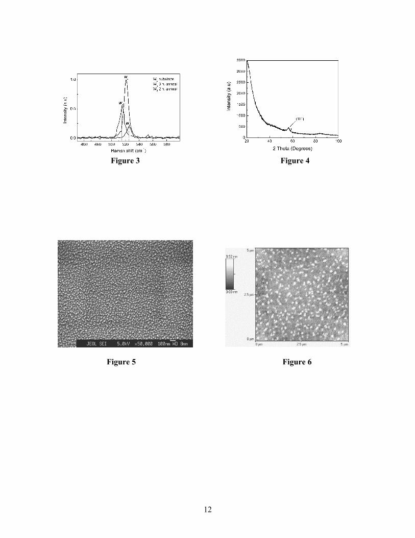
Figure 3 Figure 4
Figure 5 Figure 6
12