
ZnO epitaxial layers grown on c-sapphire substrate with MgO buffer by plasma-assisted molecular beam...
10
ZnO epitaxial layers grown on c-sapphire substrate with MgO buffer by plasma-assisted molecular beam epitaxy (P-MBE) This article has been downloaded from IOPscience. Please scroll down to see the full text article. 2005 Semicond. Sci. Technol. 20 S13 (http://iopscience.iop.org/0268-1242/20/4/002) Download details: IP Address: 142.12.73.66 The article was downloaded on 17/05/2013 at 11:57 Please note that terms and conditions apply. View the table of contents for this issue, or go to the journal homepage for more Home Search Collections Journals About Contact us My IOPscience
-
Upload
independent -
Category
Documents
-
view
4 -
download
0
Transcript of ZnO epitaxial layers grown on c-sapphire substrate with MgO buffer by plasma-assisted molecular beam...

ZnO epitaxial layers grown on c-sapphire substrate with MgO buffer by plasma-assisted
molecular beam epitaxy (P-MBE)
This article has been downloaded from IOPscience. Please scroll down to see the full text article.
2005 Semicond. Sci. Technol. 20 S13
(http://iopscience.iop.org/0268-1242/20/4/002)
Download details:
IP Address: 142.12.73.66
The article was downloaded on 17/05/2013 at 11:57
Please note that terms and conditions apply.
View the table of contents for this issue, or go to the journal homepage for more
Home Search Collections Journals About Contact us My IOPscience

INSTITUTE OF PHYSICS PUBLISHING SEMICONDUCTOR SCIENCE AND TECHNOLOGY
Semicond. Sci. Technol. 20 (2005) S13–S21 doi:10.1088/0268-1242/20/4/002
ZnO epitaxial layers grown onc-sapphire substrate with MgO buffer byplasma-assisted molecular beam epitaxy(P-MBE)M W Cho1, A Setiawan2, H J Ko3, S K Hong4 and T Yao1,5
1 Institute for Materials Research, Tohoku University, 2-1-1 Katahira, Aobaku,Sendai 980-8577, Japan2 Department of Mechanical Engineering, Indonesia University of Education,Jl. Dr Setiabudhi 207, Bandung 40154, Indonesia3 Korea Photonics Technology Institute, 459-3 Bonchon-dong, Buk-gu, Gwangju 500-210,Korea4 Department of Materials Science and Engineering, Chungnam National University,Daejeon 305-764, Korea5 Center for Interdisciplinary Research, Tohoku University Aramaki, Aoba-ku,Sendai 980-8578, Japan
E-mail: [email protected]
Received 15 September 2004Published 15 March 2005Online at stacks.iop.org/SST/20/S13
AbstractZnO films on c-sapphire with and without an MgO buffer were grown byplasma-assisted molecular beam epitaxy. ZnO with an MgO buffer was twodimensionally grown, while ZnO without an MgO buffer was grown threedimensionally, which was confirmed by in situ RHEED (reflection highenergy electron diffraction) and AFM (atomic force microscopy)observations. Morphology evolution and growth mechanism of an MgObuffer were studied by in situ RHEED observations. Mosaicity (tilt andtwist angle), type and density of dislocation were studied by both TEM(transmission electron microscopy) and HRXRD (high resolution x-raydiffraction). Based on in situ RHEED observations, MgO buffer growthinvolves three important steps including two-dimensional (2D) growth(wetting layer), 2D–3D growth transition and 3D growth. The mechanismof MgO buffer growth can be attributed to three inter-related effects. Theyare lowering surface energy through a wetting process, creating nucleationsites through a 2D–3D growth transition, and reducing the defect density byintroducing dislocation interactions. It was found that the surfacemorphology and structural properties of the ZnO layers were improved byemploying a thin MgO buffer layer grown at around 500 C followed byhigh temperature annealing at 800 C. By introducing an MgO buffer, theformation of 30 rotational domains in ZnO layers was suppressed, andscrew and edge dislocation density of ZnO layers was reduced from 6.1 ×10 8 cm−2 to 8.1 × 105 cm−2 and from 1.3 × 1010 cm−2 to 1.1 × 1010 cm−2,respectively.
0268-1242/05/040013+09$30.00 © 2005 IOP Publishing Ltd Printed in the UK S13

M W Cho et al
28"
ZnO (0002)
16.7 16.8 16.9 17.0 17.1
Inte
nsit
y (a
.u.)
From interface region
Ω (degree)
Figure 1. The 0002 rocking curve of a ZnO film grown onc-sapphire shows a long tail indicating degradation of the interfaceregion.
1. Introduction
At the current stage, the problem in extending towards ZnO-based device applications is the difficulty in achieving highcrystal quality in either bulk or thin film dimensions ofZnO. We have focused on improving the quality of ZnOfilms grown by plasma-assisted molecular beam epitaxy(P-MBE) on c-sapphire with an MgO buffer layer throughgrowth optimization and detailed structural characterization.
Because of the absence of suitable substrate materials, themain efforts for ZnO epitaxial growth have been concentratedon c-sapphire (α-Al2O3) substrate. However, the biggestobstacle to ZnO epitaxy on c-sapphire is the large latticemisfit with ZnO. The most plausible in-plane orientationrelationships between ZnO and c-sapphire are (1) [2-1-10]Al2O3//[2-1-10]ZnO, i.e., crystallography aligned, whichresults in 32% lattice misfit, and (2) [1-100] Al2O3//[2-1-10]ZnO, i.e., 30 rotated, which results in 18% lattice misfit.Hence both types of domains with an in-plane rotational angleof 30 will exist in ZnO layers grown on c-sapphire. Figure 1shows (0002) rocking curve of a P-MBE ZnO film grown onc-sapphire [1]. The line shape shows two different features,i.e., Lorenzian line shape with a full width half maximum(FWHM) of 313 (arcs), which arises from the near interfaceregion and Gaussian line shape with FWHM of 28 (arcs) fromthe ZnO overlayer. These features imply the degradation ofthe interface area caused by the presence of high defect densityat the interface.
Therefore, the growth of ZnO epitaxial films on substrateswith smaller lattice misfit is highly needed to improve thecrystal quality of ZnO films. To this end, we have studiedZnO epitaxial growth with a GaN template [2–4] and an MgObuffer layer with a low temperature (LT) ZnO buffer [5].In this paper, we review the growth and characterization ofZnO films on c-sapphire substrates with an MgO buffer usingP-MBE. In order to overcome the problems caused by thelarge mismatch between ZnO and c-sapphire, the insertionof a buffer layer material which can reduce lattice misfitbetween ZnO and c-sapphire seems to be key to obtaininghigh quality ZnO layers. The growth of double buffer layersconsisting of a low temperature (LT)-MgO buffer and a LT-ZnO buffer followed by a high temperature annealing has been
utilized with success by P-MBE [6, 7]. Here, the highlymismatched heterointerface of ZnO/α-Al2O3 (18%) is brokenup into two smaller mismatched interfaces of ZnO/MgO(9%) and MgO/α-Al2O3 (8%) by inserting an MgO layer,which eventually leads to surface adhesion and lateral epitaxialgrowth. Consequently, the growth of HT (high temperature)ZnO is dominated by layer-by-layer growth, the formationof 30-rotated domains is completely suppressed, and thedislocation density is reduced. However, the dislocationdensity still remains high, particularly in edge dislocations(higher than 5 × 109 cm−2) [8]. Therefore, the improvementof ZnO quality is one of the important issues for ZnO-baseddevice applications.
2. Growth processes
Prior to growth, the substrate was thermally cleaned at 750–800 C in the buffer chamber for 1 h. After transferringthe substrate into the growth chamber, the substrate was thentreated in oxygen plasma exposure at 700 C for 30 min toproduce an oxygen terminated c-sapphire surface. The typicalgrowth procedure was as follows. First, an MgO buffer layerwas grown on cleaned c-sapphire at 490 C with a growth rateof 0.001 nm s−1. Then, an LT-ZnO buffer layer was grown at490 C with a growth rate of around 0.002 nm s−1 followedby annealing at 750 C for 5 min. Next, an HT-ZnO layerwas grown at 700 C. The oxygen plasma flow rate was set at2.5 sccm and the plasma power at 300 W.
Figure 2 provides in situ RHEED observations duringthe growth of ZnO on c-sapphire with and without an MgObuffer layer [7]. The ZnO sample without an MgO bufferwas grown three-dimensionally as indicated by a spottyRHEED pattern at the end of the growth, while the ZnOsample with an MgO buffer was grown two-dimensionallyas indicated by a streaky RHEED pattern at the end of thegrowth (h). Furthermore, the growth of an MgO bufferinvolves three important steps including two-dimensional(2D) growth or wetting layer (b), 2D–3D growth transition(c), and 3D growth of the MgO buffer (d). The six-fold symmetry and rod spacing of the pattern (b) indicatethat rocksalt MgO grows with the [111] crystal orientationnormal to the c-sapphire plane with the following epitaxialrelationships: MgO[1-10]//α-Al2O3 [2-1-10] and MgO[-1-12]//α-Al2O3[01-10]. The 2D–3D transition naturallyresults from the 8% lattice mismatch between MgO (111) andc-sapphire. The low temperature ZnO buffer growth is startedafter a well-developed spotty pattern of the MgO buffer (d ). Aspotty pattern of ZnO (e) immediately appears, superimposingon the MgO pattern with the rod spacing about 9% smaller.After 5 min annealing at 750C, a sharp streaky RHEEDpattern of ZnO (g) appears, which marks the completion of thebuffer growth process. The growth of the ZnO layer is thenresumed at 700 C. After only a few minutes growth, an intenseRHEED specular spot appears and a (3 × 3) reconstructionpattern evolves. These features hold until the end of growth (i).According to the RHHED patterns, the epitaxial relationshipsare determined as ZnO[01-10]//MgO[1-10] and ZnO[2-1-10]//MgO[-1-12]. Here, we have shown how to achieve a flat andordered surface of ZnO layers, in which the key step is thedeposition of a thin MgO buffer.
S14

ZnO epitaxial layers grown on c-sapphire substrate with MgO buffer
ZnO/MgO/α-Al2O3
Al2O3 [1100] MgO [1110] MgO [1110] MgO [1110]
ZnO [1210] ZnO [1210] ZnO [1210] ZnO [1210]
(a) (b) (c) (d)
(e) ( f ) (g) (h)
Figure 2. Evolution of the RHEED pattern during growth of P-MBE ZnO. For ZnO/MgO/α-Al2O3. (a) Al2O3 (0001) surface afterO-plasma treatment, (b) after 2D growth MgO (wetting layer), (c) 2D–3D growth transition, (d ) 3D growth MgO, (e) after 30 s growth ofLT-ZnO, (f ) after 90 s growth of LT-ZnO, (g) after annealing and (h) after the end of the growth.
5 nm5 nmAlAl22OO33
ZnOZnO
MgOMgO bufferbuffer
Figure 3. High resolution cross-sectional TEM image of a ZnO filmgrown on c-sapphire with an MgO buffer layer. The image wasviewed along the [2-1-10]ZnO zone axis.
Figure 3 shows a cross-sectional high-resolution TEMimage of the ZnO/MgO/α-Al2O3 interface region [9]. Here,the thickness of the MgO buffer was around 3 nm. The MgObuffer is resolved into two regions. The MgO buffer layer witha thickness less than 1 nm adjacent to the α-Al2O3 substrateshows 2D morphology. Above that, the MgO buffer layer,which can be clearly distinguished from the ZnO overgrowth,displays a significant non-uniformity and a rough morphology.These two regions correspond to the 2D wetting layer and the3D island as observed by RHEED (figure 2).
As evidence of layer-by-layer growth, RHEED intensityoscillations are recorded during consecutive ZnO growth.Figure 4 shows the intensity oscillations of the RHEEDspecular spot with the incident electron beam along the ZnO[1-210] azimuth for various growth temperatures. Theobserved decrease of oscillation amplitude is due to the growthmode transition from 2D nucleation to a step-flow mode,but not due to the surface morphology degradation, sincea sharp streaky RHEED pattern with the intense specularspot becomes even clearer at higher temperatures. On thecontrary, the growth at temperatures below 400 C resultsin surface roughening. One oscillation corresponds to thedeposition of a ZnO molecular layer. The growth rate of ZnOmonotonically decreases with the substrate temperature forsubstrate temperatures from 400–800 C.
0 10 20 30 40 50 60 70 80
Tsub: substrate temperatureZn shutter open (at 10 sec)
O shutter open (at 5 sec)
Tsub = 600°C
Spec
ular
spot
inte
nsit
y (a
rb. u
nit)
Growth time (seconds)
Tsub = 550°C
Tsub = 500°C
Tsub = 450°C
Tsub = 400°C
Figure 4. The intensity oscillations of the RHEED specular spot.
Figure 5 plots the growth rate of ZnO against the Znbeam flux. The growth rate curve can be roughly divided intotwo parts. When the Zn beam flux is low, the growth rateincreases linearly with the Zn beam flux up to 0.51 nm s−1,indicating an oxygen-rich condition. While in the high Zn fluxregion, the growth rate remains constant, indicating excess Znflux. The effective oxygen flux is estimated to be equal tothe Zn beam flux at the point where the growth rate startsto saturate. The boundary between the two parts definesthe stoichiometric condition. The saturated growth rate is0.38 µm h−1. Because of the high vapour pressures of both Znand oxygen at this substrate temperature, Zn atoms only bondto oxygen atoms and vice versa on the ZnO (000-1) surface.This gives rise to the linear dependence of the growth rate onthe Zn beam flux [8, 10].
3. Surface morphology
A ZnO layer without an MgO buffer showed a spotty RHEEDpattern, indicating 3D growth mode, while a ZnO layer with
S15
M W Cho et al
0 0.1 0.2 0.3 0.4 0.5 0.6 0.7 0.8 0.9 1.00.0
0.1
0.2
0.3
0.4
0.5
0.6
Zn-rich
Stoichiometric
O-rich
Gro
wth
rat
e (µ
m/h
)
VZn (nm/s)
O-plasma: 300W, 3 sccm
Tg=700°C
Figure 5. Growth rate of ZnO layers as a function of Zn beam flux.
an MgO buffer showed a streaky RHEED pattern with adistinct specular spot, indicating 2D-growth mode. AFMimages showed that faceted crystallites with triangular shapecharacterize the morphology of ZnO layers without an MgObuffer. Such a surface should correspond to a 3D-growthmode consistent with RHEED observations. In contrast, thesurface of a ZnO layer with an MgO buffer was atomicallyflat. Hexagonal islands composed of extended terraces withbilayer steps dominate the surface, which is indicative of 2D-growth mode. The root-mean-square (rms) values of surfaceroughness at 1 µm2 scan area were 13 nm for ZnO layers grownwithout an MgO buffer and less than 1 nm for ZnO layers withan MgO buffer. Furthermore, the grain size of the ZnO layersincreased from 500 nm to 2000 nm by inserting an MgO buffer.These features indicate that the surface morphology of the ZnOlayers was greatly improved by employing a thin MgO bufferlayer.
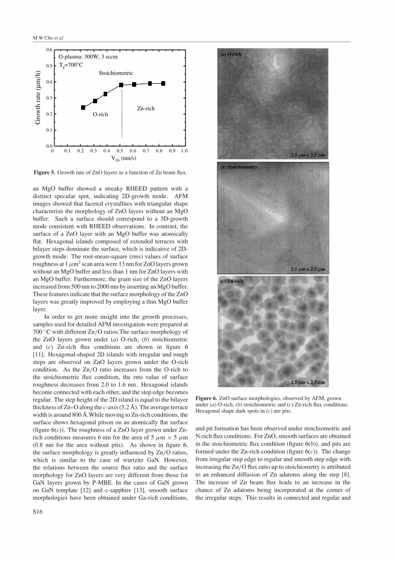
In order to get more insight into the growth processes,samples used for detailed AFM investigation were prepared at700 C with different Zn/O ratios.The surface morphology ofthe ZnO layers grown under (a) O-rich, (b) stoichiometricand (c) Zn-rich flux conditions are shown in figure 6[11]. Hexagonal-shaped 2D islands with irregular and roughsteps are observed on ZnO layers grown under the O-richcondition. As the Zn/O ratio increases from the O-rich tothe stoichiometric flux condition, the rms value of surfaceroughness decreases from 2.0 to 1.6 nm. Hexagonal islandsbecome connected with each other, and the step edge becomesregular. The step height of the 2D island is equal to the bilayerthickness of Zn–O along the c-axis (5.2 A). The average terracewidth is around 800 A.While moving to Zn-rich conditions, thesurface shows hexagonal pitson on an atomically flat surface(figure 6(c)). The roughness of a ZnO layer grown under Zn-rich conditions measures 6 nm for the area of 5 µm × 5 µm(0.8 nm for the area without pits). As shown in figure 6,the surface morphology is greatly influenced by Zn/O ratios,which is similar to the case of wurtzite GaN. However,the relations between the source flux ratio and the surfacemorphology for ZnO layers are very different from those forGaN layers grown by P-MBE. In the cases of GaN grownon GaN template [12] and c-sapphire [13], smooth surfacemorphologies have been obtained under Ga-rich conditions,
(a) O-rich
2.5 µm x 2.5 µm
2.5 µm x 2.5 µm
2.5 µm x 2.5 µm
(b) Stoichiometry
(c) Zn-rich
Figure 6. ZnO surface morphologies, observed by AFM, grownunder (a) O-rich, (b) stoichiometric and (c) Zn-rich flux conditions.Hexagonal shape dark spots in (c) are pits.
and pit formation has been observed under stoichiometric andN-rich flux conditions. For ZnO, smooth surfaces are obtainedin the stoichiometric flux condition (figure 6(b)), and pits areformed under the Zn-rich condition (figure 6(c)). The changefrom irregular step edge to regular and smooth step edge withincreasing the Zn/O flux ratio up to stoichiometry is attributedto an enhanced diffusion of Zn adatoms along the step [8].The increase of Zn beam flux leads to an increase in thechance of Zn adatoms being incorporated at the corner ofthe irregular steps. This results in connected and regular and
S16

ZnO epitaxial layers grown on c-sapphire substrate with MgO buffer
-60 0 60 120 180 240 300 360
10 2
10 4
10 6
(101-1)ZnO
Inte
nsit
y (a
rb. u
nit)
Φ scan (degree)
ZnO/MgO/c-sapphire
Figure 7. 101-1 scans of ZnO/MgO/c-sapphire. Corresponding diffraction patterns along the [0001] zone axis are given on the right side.
smooth step edges. When the Zn flux exceeds that requiredfor the stoichiometric flux condition, hexagonal pits form onthe ZnO surface. The relationship between pit formation andsource flux ratio in wurtzite ZnO and GaN seems to be relatedto the crystal polarity of the material. ZnO layers grown on c-sapphire in this work are O-polar (O-terminated) surface. Pitson O-polar ZnO surface form under Zn-rich conditions. GaNlayers grown by P-MBE on metal-organic chemical-vapourdeposition GaN templates, in which the GaN templates are Gapolar, exhibited pits under N-rich growth conditions. SurfaceZn (N) atoms have one bond to the underlying O (Ga) and threedangling bonds for the O-polar ZnO (Ga-polarGaN). The highdensity of dangling bonds reduces the mobility of O adatoms.This means that surface morphology should be determined bymobile Zn. As the growth condition is under Zn-rich on anO-polar ZnO layer, excess Zn adatoms at the step have chancesto hop onto the higher level terrace before being stabilized byoxygen. These Zn adatoms migrate to upsteps on the higherlevel terrace since the upstep is the favourable incorporationsite. This mass transport causes an initial tiny pit on the surfaceto grow up to large hexagonal pits under Zn-rich conditions onO-polar ZnO surfaces.
4. Structural characterization
4.1. Reduction of crystalline defects by an MgO buffer
In order to characterize the effects of an MgO buffer onthe quality of ZnO layers, the structural properties wereinvestigated using TEM and HRXRD. HRXRD was used toassess the crystal quality of heteroepitaxial layers includingtwins, mosaicity (tilt and twist angle) and dislocation density.Cross-sectional and plane-view TEM were used to determinetwins, type, density and distribution of dislocation. ZnO layerswere grown on c-sapphire by P-MBE either with or withoutan MgO buffer. The thickness of the ZnO layers was 450 nm.
4.1.1. Suppression of rotated domains. As is well known, thedirect growth of ZnO on c-sapphire results in the coexistenceof two types of ZnO domains which have in-plane epitaxyrelationships with c-sapphire: (1) [2-1-10]α-Al2O3//[2-1-10]ZnO, i.e., crystallography aligned, which results in 32% latticemisfit; (2) [1-100]α-Al2O3//[2-1-10] ZnO, i.e., 30 rotated,which results in 18% lattice misfit. The latter dominates theZnO layers. Figure 7 shows a typical 101-1 scan of ZnOlayers grown with an MgO buffer for 360 rotation of thesample along the surface normal. Only six peaks separated
by 60 appear, which clearly indicates that the sample hassix-fold symmetry around the c-axis. This indicates thatthere are no rotated domains in the ZnO layer with an MgObuffer. In contrast, ZnO without an MgO buffer showed smalldiffraction peaks at the mid angle between the adjacent peaksseparated by 60 in the 101-1 scan, which is due to thepresence of 30-rotated domains. In quite a few cases, twolow intensity peaks appeared between every two high intensitypeaks. The low intensity peaks were separated by 20 each,indicating the formation of 20-rotated domains. Althoughthe mechanism of the formation of 20-rotated domains is notyet well understood, this is likely caused by the large misfitbetween ZnO and c-sapphire.
4.1.2. Reduction of dislocations. The most commondislocations in ZnO films grown on c-sapphire substrates arerunning parallel to the [0001] growth direction. They showedge, screw and mixed character with Burgers vector b =1/3〈112-0〉, 〈0001〉 and 1/3〈112-3〉, respectively. In orderto address the defect structures of wurzite ZnO by HRXRD,0002 and 101-1 and rocking curves measurements wereperformed. Note that the broadening of 0002 and 101-1
rocking curves represent lattice disordering along the growthdirection (out of plane) and in-plane disordering, respectively.
Figure 8 shows a comparison of (a) 0002 and (b) 101-1 rocking curves of ZnO layers grown with and withoutan MgO buffer. The FWHM values of 0002 scan are565 and 18 (arcs) for ZnO grown without and with an MgObuffer, respectively. The FWHM values of 101-1 scan are1346 and 1076 (arcs), respectively. It should be noted herethat the FWHM of the 0002 scan was greatly reduced byemploying an MgO buffer layer. This indicates a small tilt inthe c-plane because of the extreme ordering along the growthdirection of ZnO (0001) as a consequence of well-controlledlayer-by-layer epitaxial growth. Significant broadening of the101-1 reflection as compared to the 0002 is indicative of thepresence of high edge dislocation density. Note that all typesof dislocations (edge, screw and mixed) broaden the 101-1reflection, whereas the 0002 reflection is only sensitive toscrew and mixed type dislocations. Furthermore, the FWHMvalue of the 101-11 scan of ZnO grown with an MgO bufferis smaller than that without MgO, indicating a much loweredge dislocation density.
4.1.3. Tilt and twist angle determination of ZnO. In order toevaluate the mosaic angle and dislocation density, rocking
S17

M W Cho et al
(a)
-0.4 -0.2 0.0 0.2 0.4
0.0
0.2
0.4
0.6
0.8
1.0
1.2
(0002) ZnO
ZnO/α-Al2O3 (FWHM = 565 arcsec)N
orm
aliz
ed in
tens
ity
(a.u
.)N
orm
aliz
ed in
tens
ity
(a.u
.)ZnO/MgO/α-Al2O3 (FWHM = 18 arcsec)
-2.0 -1.6 -1.2 -0.8 -0.4 0.0 0.4 0.8 1.2 1.6 2.0
0.0
0.2
0.4
0.6
0.8
1.0
1.2
Ω scan (degree)
Ω scan (degree)
ZnO/α-Al2O3 (FWHM = 1346 arcsec)ZnO/MgO/α-Al2O3 (FWHM = 1076 arcsec)
(101-1) ZnO
Figure 8. Comparison of (a) 0002 and (b) 101-1 scans of aZnO layer grown without (dotted curve) and with (solid curve) anMgO buffer.
curve scans of 0002, 0004, 0006, 10-13, 10-12, 10-11, 303-2reflections and a scan of 10-11 reflection are performed.Figure 9 shows the typical Williamson–Hall (WH) plot ofZnO samples with and without an MgO buffer. From the leastsquare fit of the WH plot for 0002, 0004, 0006 scans, where‘FWHM × sin (θ)/λ’ is plotted against ‘sin (θ)/λ’, the tiltangle can be determined [8, 14]. Here θ is the diffractionangle and λ is the wavelength of Cu Kα (0.154 056 nm).The tilt angles are estimated as 0.1541 and 0.0056 for ZnOsamples without and with an MgO buffer, respectively. Inorder to determine the twist angle, FWHMs of 0002, 101-3,101-2, 101-1, 303-2 scans were plotted as a function of theinclination angles. The twisted angles are determined to be0.4387 and 0.4108, respectively, for ZnO layers without andwith an MgO buffer.
The twist angle can be determined by using other methods.In order to do so, a 101-1 scan is performed because the scan represents the twist angle. Metzger et al have usedthe FWHM of a 101-5 scan to estimate the twist angle inGaN films on c-sapphire [15]. However, it should be notedthat the twist angle is caused by 1/3〈11-20〉 edge dislocationand hence, it might be more effectively revealed by a 101-1 scan rather than a 101-5 scan because the in-planecomponent of displacement by 1/3〈11-20〉 edge dislocationswould be pronouncedly recognized by the 10-11 scan. Thetwist angles estimated by the 10-11 scan were 0.3804 and0.3655, respectively, for ZnO films without and with an MgObuffer. Here, these values are nearly the same as twist anglesdetermined from a symmetric skew scan (0.4387 and 0.4108,respectively). Our results imply that evaluation by the 10-11 scan is reliable enough to be used as a routine evaluation
(006)
(004)
(002)
ZnO/MgO/Al2O3
0.0
4.0x10⁻⁴
8.0x10⁻⁴
1.2x10⁻³
1.6x10⁻³
2.0x10⁻³
2.4x10⁻³
FWH
Mx
sin
(θ)/λ
0.0 0.1 0.2 0.3 0.4 0.5 0.6 0.7
sin (θ)/ λ
(006)
(004)
(002)
ZnO/Al2O3
Tilt angle: 0.1541 [deg.]
Tilt angle: 0.0056 [deg.]
0.0 0.1 0.2 0.3 0.4 0.5 0.6 0.7
sin (θ)/λ
0.0
4.0x10⁻⁴
8.0x10⁻⁴
1.2x10⁻³
1.6x10⁻³
2.0x10⁻³
2.4x10⁻³
FWH
Mx
sin
(θ)/λ
(a)
(b)
Figure 9. Williamson–Hall plots for a ZnO layer on a c-sapphire(a) with and (b) without an MgO buffer.
method for twist angles with a shorter measuring time ratherthan the more complex skew scan. From the determined tiltangle, screw dislocation densities are determined as 6.1×10⁸
cm−2 and 8.1×105 cm−2 respectively, for a ZnO layer withoutand with an MgO buffer. Here, the screw dislocation densityof a ZnO layer was greatly reduced by about three orders ofmagnitude by employing an MgO buffer. From the determinedtwist angles, edge dislocation densities are determined to be1.3 × 1010 cm−2 and 1.1 × 1010 cm−2, for a ZnO layer withoutand with an MgO buffer, respectively. The edge dislocationsdensity is slightly reduced by employing an MgO buffer layer.The low screw dislocation density in a ZnO layer with an MgObuffer implies good ordering in the growth direction while thehigh edge dislocation density means high disorder in the c-plane.
4.1.4. Dislocation characterizations by TEM. The typesof dislocation in ZnO samples with and without an MgObuffer were further characterized by cross-sectional TEM withinvisibility criterion under a two-beam condition, as shown infigure 10. The samples were observed near the [21-1-0] zoneaxis with diffraction vectors g = 0006 (figures 10(a) and (c))and g = 03-30 (figures 10(b) and (d)). By the invisibilitycriterion, screw-type dislocations should be visible under g =0006 but invisible under g = 03-30. In contrast, the edge-typedislocation should be invisible under g = 0006 but visibleunder g = 03-30. While mixed-type dislocations should bevisible under both g vectors. By averaging several pictures forthe ZnO layer without an MgO buffer, threading dislocations(TDs) were roughly distributed as 31% of screw-type (Burgers
S18

ZnO epitaxial layers grown on c-sapphire substrate with MgO buffer
200 nm200 nm
g(a)
ZnO
Al2O3
200 nm200 nm
gg
ZnO
Al2O3
200 nm200 nm
g
ZnO
Al2O3
200 nm200 nm
gg
ZnO
Al2O3
ZnO/Al2O3
ZnO/Al2O3
ZnO/MgO/Al2O3
ZnO/MgO/Al2O3
(b)
(c)
(d)
Figure 10. Two-beam bright-field cross-sectional electronmicrographs of the ZnO/α-Al2O3 near the [2-1-10] zone axis withg = 0006 ((a) and (c)) and g = 03-30 ((b) and (d)).
vector b = [0001]), 61% of edge-type (Burgers vectors b =1/3 〈11-20〉) and 8% of mixed-type (Burgers vectors b =1/3 〈11-23〉) dislocations. While for the ZnO layer withMgO, the threading dislocations were distributed as 98% ofedge-type and 2% of screw-type and mixed-type dislocations.Here, the major threading dislocations running along the c-axis are edge-type dislocations with the Burgers vector of1/3〈11-20〉 in both types of samples. A comparison offigures 10(a) and (c) reveals that the screw dislocations weregreatly reduced by introducing an MgO buffer, consistentwith the XRD evaluation. Figure 10 shows anotherimportant aspect. At the interface region, a high density ofinterfacial threading dislocations was observed. Surprisingly,the dislocation density rapidly decreases above 50 nm.Furthermore, the density of these threading dislocationsdecreases faster in a ZnO layer with an MgO buffer thanwithout an MgO buffer. It can only be understood if thesethreading dislocations are not along the c-axis so that theystrongly interact with each other and annihilate quickly [5].Since favourable dislocation in MgO with fcc lattice doesnot run along the c-axis, much stronger interaction betweendislocations might be introduced when ZnO initially nucleatedonto MgO, which leads to a reduction in dislocation density.Furthermore, lattice misfit between ZnO and MgO (9%)is smaller than that between ZnO and c-sapphire (18%).Therefore, the density of interfacial defects in ZnO with anMgO buffer is smaller than that without an MgO buffer.
4.2. Effects of Zn/O flux ratio on defect generation
Examining the XRD data, figure 11 shows the FWHM valuesof (0002) and (10-10) rocking curves versus the Zn
0.0 0.1 0.2 0.3 0.4 0.5 0.6 0.7 0.8 0.9 1.0
0
200
400
600
800
1000
1200
1400
1600
1800
2000
O-plasma: 300W, 3 sccm
(0002) ZnO
(10-10) ZnO
FWH
M o
f X
RC
(ar
csec
)
VZn (nm/s)
Tg=700°C
Figure 11. The FWHM values of (0002) (solid squares) and(10-10) (solid circles) rocking curves of ZnO layers versus Znbeam flux.
beam fluxes [16]. The significant broadening of the (10-10)reflection as compared with the (0002) reflection is anindication of the presence of a high density of edge-typedislocations. Note that edge dislocations broaden the (10-10)reflection, whereas the (0002) reflection is sensitive to screwand mixed-type dislocations. The FWHM value of the (10-10) rocking curve decreases as the Zn beam flux is increasedup to 0.51 nm s−1, a stoichiometric flux condition, and thenremains nearly constant over Zn-rich flux conditions, while theFWHM value of the (0002) scan is low and nearly constantfor various Zn beam fluxes. The HRXRD data show thatstoichiometric and Zn-rich grown ZnO have better crystallinequality than O-rich grown ZnO. This feature is consistent witha previous report [17].
Dislocation features in ZnO layers grown with differentflux ratios were imaged by cross-sectional TEM under a two-beam condition with invisibility criterion, g · b = 0, as shownin figure 12. The samples were observed near the [10-10] zoneaxis with diffraction vectors g = 0004 (images (a), (c) and (e))and g = 2-1-10 (images (b), (d) and (f )). For all the samples,the threading dislocations are invisible under g = 0004 andvisible under g = 2-1-10. This feature indicates that a majorityof the TDs are edge-type dislocations running along the c-axiswith Burgers vectors of 1/3〈11-20〉. The same feature wasreported in previous papers about ZnO on c-sapphire with anMgO buffer [5]. By averaging several pictures, TD densitiesare determined to be 6.9 × 109 cm−2, 2.8 × 109 cm−2, and 2.7 ×109 cm−2, for O-rich, stoichiometric and Zn-rich grown ZnO,respectively. The dislocations density, D, was determined bythe formula D = n/lh, where n = the number of dislocations,l = foil length and h = foil thickness. The foil thickness wasdetermined by measuring the number of extinction distancefringes for two-beam, s = 0, g = 0002, images and usingthe extinction distance as a reference for the crystal thicknesschange with each fringe.We should note that both the HRXRDand TEM data show that stoichiometric and Zn-rich grownZnO have much better crystalline quality than O-rich grownZnO. Figure 12 shows other interesting features. Differentfrom the O-rich grown ZnO where the dislocations are runningalong the c-axis, several dislocations in stoichiometric and Zn-rich grown ZnO are inclined 20 –30 from the c-axis (whitearrows).
S19

M W Cho et al
200 nm
g
g
Zn-rich
g
g
200 nm
g
(a)
(b)
O-rich
Al2O3
ZnO200 nm200 nm
200 nm
g
Stoichiometric (c)
(d)
(e)
( f )
Figure 12. Cross-sectional TEM images of ZnO layers grown under different Zn/O flux ratios viewed along the [01-10] zone axis. The g =0004 imaging condition was used for (a), (c) and (e) and g = [2-1-10] imaging condition was used for (b), (d) and (f ).
-11)-11)
(b) Stoichiometricand Zn-rich
(a) O-rich
(1010)
b = [1120]
(1011)
Figure 13. Schematic illustration of the slip plane, dislocation lineand Burgers vectors for (a) O-rich grown ZnO and(b) stoichiometric and Zn-rich grown ZnO.
Figure 13 shows a schematic illustration of the slip plane,dislocation line and Burgers vectors for (a) O-rich grown ZnOand (b) stoichiometric and Zn-rich grown ZnO. Since the edgedislocation line should be perpendicular to the Burgers vector,by considering the direction of dislocation line we concludedthat the glide planes of the dislocations are close to 10-10for O-rich grown ZnO (a) and close to 10-11 for thestoichiometric and Zn-rich grown ZnO (b). Note that theBurgers vector of the edge dislocation is 1/3〈11-20〉.
Now let us discuss dislocations near the interface.Figure 14 shows the edge component of TDs near the interface.Near the interface, highly faulted regions as well as basaldislocations located on the basal plane were observed in allthe samples. However, the density rapidly decreases beyond50 nm from the interface. This can only be understood ifthese dislocations are not oriented along the c-axis so that they
g
Inclined dislocation
30o
gInterface dislocation
(a)
(b)
g
Inclined dislocation
(c)
Figure 14. Magnified images of edge components of TDs in ZnOgrown under (a) O-rich, (b) stoichiometric and (c) Zn-rich fluxconditions. The images were viewed along the [10-10] zone axiswith g = [2-1-10].
can strongly interact with each other and annihilate quickly[9]. The thickness of the basal TDs in O-rich grown ZnO(figure 14(a)) is thinner than that of stoichiometric and Zn-richgrown ZnO (figures 14(b) and (c)). Beyond 50 nm thickness,we observe the generation of TDs running along the c-axis.The TDs density is reduced in the upper ZnO layer. Basically,TDs can be reduced by the reaction with other TDs. Thetwo reduction reactions are annihilation (half-loop dislocation)
S20

ZnO epitaxial layers grown on c-sapphire substrate with MgO buffer
in which the TDs with the opposite Burgers vectors meet,and fusion (inverted ‘Y’ dislocation) in which two TDs withdifferent but suitable Burgers vectors meet each other andcombine into a single dislocation. The presence of the inclineddislocations in stoichiometric and Zn-rich ZnO layers allowsfor dislocation interaction to form single dislocations or toannihilate, leading to a reduction of dislocation density in theupper ZnO layers.
5. Conclusion
ZnO films were grown on c-sapphire with and without an MgObuffer by P-MBE (plasma-assisted molecular beam epitaxy).ZnO with an MgO buffer was two-dimensionally grown, whileZnO without an MgO buffer was grown three-dimensionallyas confirmed by RHEED and AFM. Based on in situ RHEEDobservations, the MgO buffer growth involves three importantsteps including 2D growth (wetting layer), 2D–3D growthtransition and 3D growth. The mechanism of the MgObuffer growth can be attributed to three inter-related effectswhich include: (1) lowering the surface energy through awetting process; (2) creating nucleation sites through a 2D–3D growth transition; and (3) reducing the defect density byintroducing dislocation interactions. It was found that thesurface morphology and structural properties of ZnO layerswere improved by employing a thin MgO buffer layer grownat around 500 C followed by high temperature annealing at800 C. By introducing an MgO buffer, the formation of 30
rotational domains in ZnO layers was suppressed, and thescrew and edge dislocation density of ZnO layers was reduced
from 6.1 × 108 cm−2 to 8.1 × 105 cm−2 and from 1.3 ×1010 cm−2 to 1.1 × 1010 cm−2, respectively.
References
[1] Chen Y, Bagnall D M, Ko H, Park K, Hiraga K, Zhu Z andYao T 1998 J. Appl. Phys. 84 3912
[2] Hong S K, Ko H J, Chen Y, Hanada T and Yao T 2000Appl. Surf. Sci. 159/160 441
[3] Ko H J, Chen Y, Yao T, Myazima K, Yamamoto A and Goto T2000 Appl. Phys. Lett. 77 537
[4] Hong S K, Hanada T, Ko H J, Chen Y and Yao T 2002Phys. Rev. B 65 115331
[5] Miyamoto K, Sano M, Kato H and Yao T 2004 J. Cryst.Growth 265 34
[6] Chen Y, Ko H J, Hong S K and Yao T 2000 Appl. Phys. Lett.76 559
[7] Chen Y, Ko H J, Hong S K, Yao T and Segawa Y 2000 J.Cryst. Growth 214/215 87
[8] Chen Y, Ko H J, Hong S K, Segawa Y and Yao T 2002Appl. Phys. Lett. 80 1358
[9] Chen Y, Ko H J, Hong S K, Kirshner V, Wenisch H, Yao T,Inaba K and Segawa Y 2001 Appl. Phys. Lett. 78 3352
[10] Yao T and Maekawa M 1981 J. Cryst. Growth 53 422[11] Ko H J, Chen Y f, Hong S K and Yao T 2002 J. Appl. Phys. 92
4354[12] Tarsa E J, Heying B, Wu X H, Fini P, DenBaars S P and
Speck J S 1997 J. Appl. Phys. 82 5472[13] Yu Z et al 1996 Appl. Phys., NY 69 2731[14] Williamson G K and Hall W H 1953 Acta Metall. 1 22[15] Metzger T et al 1998 Phil. Mag. A 77 1013[16] Kato H H, Sano M, Miyamoto K and Yao T 2004 Phys. Status
Solidi b 241 612[17] Ko H J, Chen Y, Hong S K and Yao T 2002 J. Appl. Phys. 92
4354
S21


![Growth model for plasma-assisted molecular beam epitaxy of N-polar and Ga-polar In[sub x]Ga[sub 1-x]N](https://static.fdokumen.com/doc/165x107/6316ef5b0f5bd76c2f02b44a/growth-model-for-plasma-assisted-molecular-beam-epitaxy-of-n-polar-and-ga-polar.jpg)