Fabrication of zinc oxide nanoparticles and films by banana ...
Upload
khangminh22Category
view
1download
0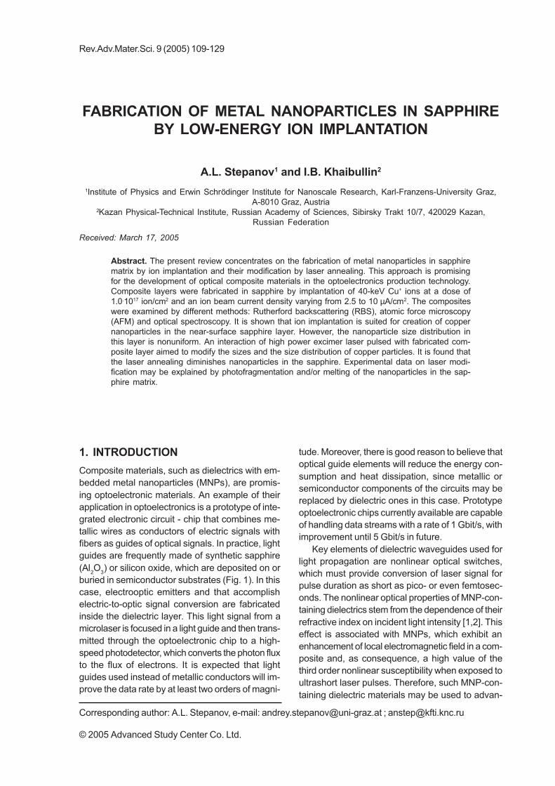
109Fabrication of metal nanoparticles in sapphire by low-energy ion implantation
Corresponding author: A.L. Stepanov, e-mail: [email protected] ; [email protected]
Rev.Adv.Mater.Sci. 9 (2005) 109-129
© 2005 Advanced Study Center Co. Ltd.
FABRICATION OF METAL NANOPARTICLES IN SAPPHIREBY LOW-ENERGY ION IMPLANTATION
A.L. Stepanov1 and I.B. Khaibullin2
1Institute of Physics and Erwin Schrödinger Institute for Nanoscale Research, Karl-Franzens-University Graz,A-8010 Graz, Austria
2Kazan Physical-Technical Institute, Russian Academy of Sciences, Sibirsky Trakt 10/7, 420029 Kazan,Russian Federation
Reñeived: March 17, 2005
Abstract. The present review concentrates on the fabrication of metal nanoparticles in sapphirematrix by ion implantation and their modification by laser annealing. This approach is promisingfor the development of optical composite materials in the optoelectronics production technology.Composite layers were fabricated in sapphire by implantation of 40-keV Cu+ ions at a dose of1.0.1017 ion/cm2 and an ion beam current density varying from 2.5 to 10 µA/cm2. The compositeswere examined by different methods: Rutherford backscattering (RBS), atomic force microscopy(AFM) and optical spectroscopy. It is shown that ion implantation is suited for creation of coppernanoparticles in the near-surface sapphire layer. However, the nanoparticle size distribution inthis layer is nonuniform. An interaction of high power excimer laser pulsed with fabricated com-posite layer aimed to modify the sizes and the size distribution of copper particles. It is found thatthe laser annealing diminishes nanoparticles in the sapphire. Experimental data on laser modi-fication may be explained by photofragmentation and/or melting of the nanoparticles in the sap-phire matrix.
1. INTRODUCTION
Composite materials, such as dielectrics with em-bedded metal nanoparticles (MNPs), are promis-ing optoelectronic materials. An example of theirapplication in optoelectronics is a prototype of inte-grated electronic circuit - chip that combines me-tallic wires as conductors of electric signals withfibers as guides of optical signals. In practice, lightguides are frequently made of synthetic sapphire(Al
2O
3) or silicon oxide, which are deposited on or
buried in semiconductor substrates (Fig. 1). In thiscase, electrooptic emitters and that accomplishelectric-to-optic signal conversion are fabricatedinside the dielectric layer. This light signal from amicrolaser is focused in a light guide and then trans-mitted through the optoelectronic chip to a high-speed photodetector, which converts the photon fluxto the flux of electrons. It is expected that lightguides used instead of metallic conductors will im-prove the data rate by at least two orders of magni-
tude. Moreover, there is good reason to believe thatoptical guide elements will reduce the energy con-sumption and heat dissipation, since metallic orsemiconductor components of the circuits may bereplaced by dielectric ones in this case. Prototypeoptoelectronic chips currently available are capableof handling data streams with a rate of 1 Gbit/s, withimprovement until 5 Gbit/s in future.
Key elements of dielectric waveguides used forlight propagation are nonlinear optical switches,which must provide conversion of laser signal forpulse duration as short as pico- or even femtosec-onds. The nonlinear optical properties of MNP-con-taining dielectrics stem from the dependence of theirrefractive index on incident light intensity [1,2]. Thiseffect is associated with MNPs, which exhibit anenhancement of local electromagnetic field in a com-posite and, as consequence, a high value of thethird order nonlinear susceptibility when exposed toultrashort laser pulses. Therefore, such MNP-con-taining dielectric materials may be used to advan-
110 A.L. Stepanov and I.B. Khaibullin
tage in integrated optoelectronic devices, for ex-ample, as shown in Fig. 1.
It is well known [1] that a local field enhance-ment in MNPs stimulates a strong linear opticalabsorption called as surface plasmon resonance(SPR). The electron transitions responsible for plas-mon absorption in MNPs cause also a generationof an optical nonlinearity of a composite in the samespectral range. As a result, the manifestation ofnonlinear optical properties is most efficient for wave-lengths near the position of a SPR maximum. Inpractice, to reach the strong linear absorption of acomposite in the SPR spectral region, attempts aremade to increase the concentration (filling factor) ofMNPs. Systems with a higher filling factor offer ahigher nonlinear susceptibility, when all other pa-rameters of composites being the same [1].
There is variety of ways to synthesis MNPs indielectrics, such as magnetron sputtering, the con-vective method, ion exchange, sol�gel deposition,etc. One of the most promising enhanced fabrica-tion methods is ion implantation (II) [3,4] because itby ion implantation allows reaching a high metalfilling factor in an irradiated matrix beyond the equi-librium limit of metal solubility and provides control-lable synthesis of MNPs at various depths underthe substrate surface. Nearly any metal�dielectriccomposition may be produced using II. This methodallows the strict control of the doping ion beam po-sition on the sample surface with implant dose as,for example, in the case of ion-beam lithography.
Today, II is widely used in industrial semicon-ductor chip fabrication. Therefore, the combination
Fig. 1. A prototype of optoelectronic chip with sapphire waveguide on silicon substrate. Ion implantation canbe applied to form selective area doped by rear metal ions (illustrated by stars) to work as micro laser andto saturate waveguide, created by He-ion irradiation with metal nanoparticles to form an optical switcher.
of MNP-containing dielectrics with semiconductorsubstrates by same technological approach as IIcould be reached quite effective. Moreover, II can beapplied for different steps in optoelectronic materialfabrication such as creation of optical waveguidesby implantation with rear gas ions (H+,He+, etc.) [3],a designing of electric-to-optic signal convectors andmicrolaser by irradiation of dialectics waveguideswith rear metal ions (Er+, Eu+, etc.) [3,5] and a syn-thesis of metal nanoparticles as discussing in thisarticle (Fig. 1).
The history of MNP synthesis in dielectrics by IIdates back to 1973, when a team of researchers J.Davenas et al. at the Lyons University (France) pio-neered this method to create particles of variousmetals (silver, sodium, calcium, etc.) in LiF and MgOionic crystals [6,7]. Later, in II practice MNPs weresuccessfully fabricated in various materials, suchas polymers, glass, artificial crystals, and miner-als. In this work, the ion synthesis of MNPs in syn-thetic sapphire (Al
2O
3) is considered, since this sub-
strate as a dielectric matrix containing MNPs hasbeen studied to a much smaller degree than standardoptical waveguide materials, e.g., silicon dioxide.
As follows from the currently available publica-tions concerning ion synthesis of MNPs in Al
2O
3
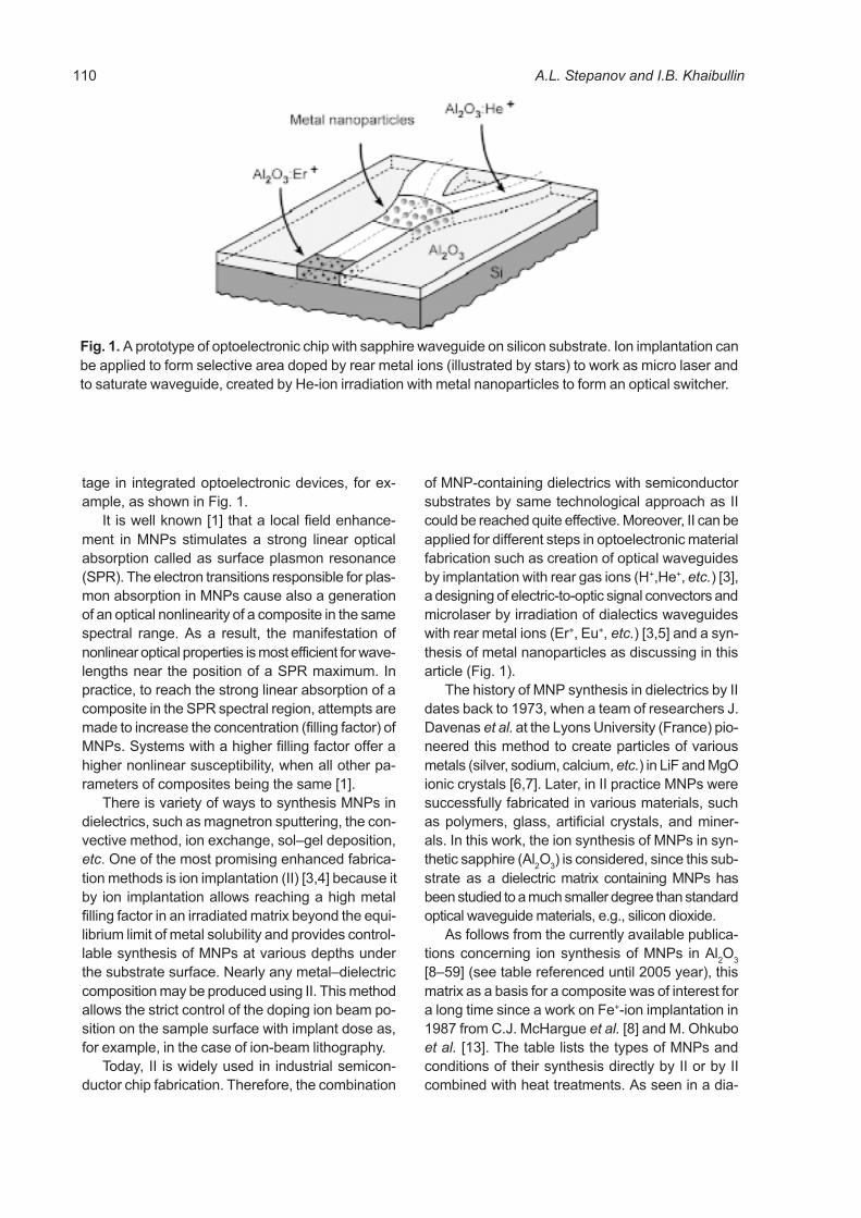
[8�59] (see table referenced until 2005 year), thismatrix as a basis for a composite was of interest fora long time since a work on Fe+-ion implantation in1987 from C.J. McHargue et al. [8] and M. Ohkuboet al. [13]. The table lists the types of MNPs andconditions of their synthesis directly by II or by IIcombined with heat treatments. As seen in a dia-
111F
abrication of metal nanoparticles in sapphire by low
-energy ion implantation
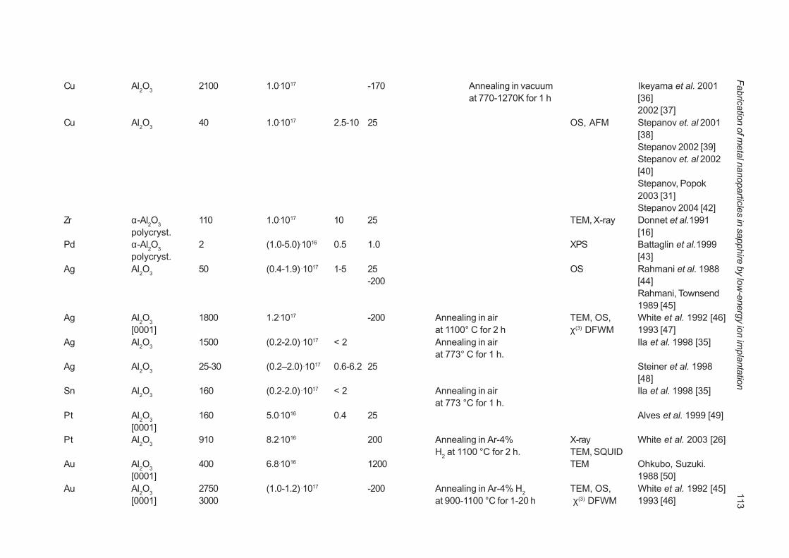
Metal of Matrix type Ion beam Ion dose Ion curent Matrix Post-implantation Methods of Authorsparticles energy, ion/cm2 density, temeperature, heat treatment particle
keV µÀ/ñì2 °Ñ indefication
α-Fe α-Al2O
3100 4.0.1016 -200 TEM, X-ray, McHargue et al.1987
[0001] 160 7.0.1016 25 CEMS [8]2.0.1017 1990 [9]
1991 [10]1996 [11]1998 [12]
α-Fe α-Al2O
3400 1.0.1017 240 Annealing in vacuum TEM, XRD Ohkubo et al.1987
[0001] at 700-1200 °C for 1 h. VSM [13]1989 [14]
α-Fe α-Al2O
3160 4.0.1016 45 Annealing in Ar-4% H
2Farlow et al.1990
[0001] at 1500 °C for 1 h. [15]α-Fe α-Al
2O
3110 1.0.1017 10 25 TEM Donnet et al.1991
polysrict. [16]α-Fe α-Al
2O
3160 1.0.1017 2 25 Sklad et al.1992 [17]
[0001]Fe α-Al
2O
360 (0.2�1.2).1017 2 Jang et al.1997 [18]
polycrist.Fe Al
2O
385 4.0.1016 10-15 25 RM Kobayashi et al 1998
[0001] 7.0.1016 [19]1.0.1017
Fe Al2O
3380 1.0.1017 2 RM Kobayashi, Terai
4.0.1017 1998 [20]1.0.1018
Table. Types of metal nanoparticles and conditions for their synthesis in Al2O
3 by ion implantation combined with post-implantation heat treatments. (Abbreviations
� TEM, transmission electron microscopy; XPS, X-ray photoelectron spectroscopy; CEMS, conversion electron Mossbauer spectroscopy; XRD, X-ray diffraction;VSM, vibrating sample magnetometry; RM, resistive measurements; GIXRD, glancing incidence X-ray diffraction; SQUID, superconducting quantum-interference-device, magnetometer; OS, optical spectroscopy; AFM, atomic-force microscopy; MR, magnetoresistance measurements; and LFRS, low frequency Raman scat-tering; χ(3) DFWM, measurements of the third-order nonlinear optical susceptibility by a degenerate four-wave mixing. The ions are listed in the order they follow in thePeriodic Table of elements).
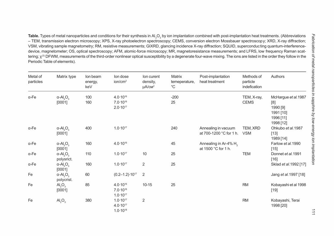
112A
.L. Stepanov and I.B
. Khaibullin
α-Fe α-Al2O
3100 (1.0-2.0).1017 2-3 25 CEMS Sakamoto et al.1999
[21]Hayashi et al. 2002[22]Wakabayashi et al.2002 [23]
Fe α-Al2O
3160 1.0.1017 25 TEM, GIXRD, Alves et al. 2002 [24]
[0001] 4.0.1017 VSM[1120]
Fe α-Al2O
3160 1.0.1017 Monteiro et al. 2002
4.0.1017 [25]Fe Al
2O
3350 1.0.1017 -200 Annealing in Ar-4% X-ray White et al. 2003
[26]25 H
2 at 1100 °C for 2 h. TEM, SQUID
α-Fe α-Al2O
3150 1.0.1017 25 TEM, CEMS McHargue et al.2004
[0001] [27]α-Fe α-Al
2O
3150 1.0.1017 25 Annealing in Ar-4% H
2TEM, CEMS McHargue et al.2004
[0001] 1000 at 1100 °C for 1 h. [27]Co α-Al
2O
320 (0.5-5.0) .1017 25 Saito et al. 1991 [28]
Co α-Al2O
3150 5.0.1017 25 SQUID, OS Marques et al. 2001
<0001> [29]<0221> 2002 [30]<1120>
Co Al2O
3140 8.0.1016 25 Annealing in Ar-4% H
2TEM, X-Ray, Meldrum et al. 2003
-100 at 1100 °C for 2 h SQUID [31]Ni α-Al
2O
3160 4.0.1016 45 Annealing in Ar-4% H
2Farlow et al.1990
[0001] at 1500 °C for 1 h. [15]Ni Al
2O
33000 1.6.1018 1 20-250 MR Kobayashi et al.1996
[1120] [32]Ni α-Al
2O
364 1.0.1017 0.5 TEM, X-ray Xiang et al.2004 [33]
2004 [34]Cu α-Al
2O
3110 1.0.1017 10 25 TEM Donnet et al.1991
polysrict. [16]Cu Al
2O
3160 (0.2-.0).1017 < 2 Annealing in air Ila et al. 1998 [35]
at 673 °C for 1 h
113F
abrication of metal nanoparticles in sapphire by low
-energy ion implantation
Cu Al2O
32100 1.0.1017 -170 Annealing in vacuum Ikeyama et al. 2001
at 770-1270K for 1 h [36]2002 [37]
Cu Al2O
340 1.0.1017 2.5-10 25 OS, AFM Stepanov et. al 2001
[38]Stepanov 2002 [39]Stepanov et. al 2002[40]Stepanov, Popok2003 [31]Stepanov 2004 [42]
Zr α-Al2O
3110 1.0.1017 10 25 TEM, X-ray Donnet et al.1991
polycryst. [16]Pd α-Al
2O
32 (1.0-5.0).1016 0.5 1.0 XPS Battaglin et al.1999
polycryst. [43]Ag Al
2O
350 (0.4-1.9) .1017 1-5 25 OS Rahmani et al. 1988
-200 [44]Rahmani, Townsend1989 [45]
Ag Al2O
31800 1.2.1017 -200 Annealing in air TEM, OS, White et al. 1992 [46]
[0001] at 1100° C for 2 h χ(3) DFWM 1993 [47]Ag Al
2O
31500 (0.2-2.0) .1017 < 2 Annealing in air Ila et al. 1998 [35]
at 773° C for 1 h.Ag Al
2O
325-30 (0.2�2.0) .1017 0.6-6.2 25 Steiner et al. 1998
[48]Sn Al
2O
3160 (0.2-2.0) .1017 < 2 Annealing in air Ila et al. 1998 [35]
at 773 °C for 1 h.Pt Al
2O
3160 5.0.1016 0.4 25 Alves et al. 1999 [49]
[0001]Pt Al
2O
3910 8.2.1016 200 Annealing in Ar-4% X-ray White et al. 2003 [26]
H2 at 1100 °C for 2 h. TEM, SQUID
Au Al2O
3400 6.8.1016 1200 TEM Ohkubo, Suzuki.
[0001] 1988 [50]Au Al
2O
32750 (1.0-1.2) .1017 -200 Annealing in Ar-4% H
2TEM, OS, White et al. 1992 [45]
[0001] 3000 at 900-1100 °C for 1-20 h χ(3) DFWM 1993 [46]
114A
.L. Stepanov and I.B
. Khaibullin
Au Al2O
32750 2.2.1016 Annealing in Ar+4%H
2Henderson et al.
[0001] at 1100 °C 1 h. 1995 [51]Au Al
2O
32000 (0.2-2.0) .1017 < 2 Annealing in air Ila et al. 1998 [36]
at 973-1323 °C for 1 h.Au Al
2O
3160 1.0.1017 OS Marques et al. 2004
[52]Au c-Al
2O
31800 (0.1�1.0) .1018 1.2 Annealing at 1000 °C OS, LFRS Dhara et al. 2004
and 1200°C for 1 h [53]Eu Al
2O
3400 1.0.1016 8 34 Annealing in air at 1200 °C Can et al. 1994 [54]
16 for 1 h 1995 [55]FeCo α-Al
2O
3100 (1.0-2.0) .1017 2-3 25 CEMS Sakamoto et al.
VSM, MR 1999 [21]Hayashi et al. 2002[22]2003 [56]
FePt α-Al2O
3Fe-350 Fe-1.0.1017 Fe� 200-550 Annealing in Ar+4% H
2SQUID, Vallet et al. 2002 [57]
Pt-910 Pt-(0.5-1.1).1017 Pt-200,500 at 1100 °C for 2 h TEM, X-ray White et al. 2002 [58]2003 [26]
CoPt α-Al2O
3Co-325 (0.5-1.0) .1017 200, 500 Annealing in Ar+4% H
2SQUID, Withrow et al. 2003
P-910 at 1100 °C for 2 h TEM, X-ray [59]

115Fabrication of metal nanoparticles in sapphire by low-energy ion implantation
Fig. 2. Attendance of papers in the literature onsynthesis of metal nanoparticles in sapphire matrixby ion implantation until 2005 year.
gram (Fig. 2), a number of publications on MNPsfabrication in Al
2O
3 by II continuously increases dur-
ing last years. This fact clearly demonstrates a wideinterest in the study of this topic; various scientificgroups are working now in this field and KazanPhysical-Technical Institute of the Russian Acad-emy of Sciences, Instituto Tecnologe Nuclear (Por-tugal), University of Tennessee-Knoxville and OakRidge National laboratory (USA), Musashi Instituteof Technology (Japan), Goteborg University andChalmers University of Technology (Sweden) shouldbe mentioned as the active participants of theseinvestigations.
As seen in the Table, while MNP synthesis inAl
2O
3 has been extensively explored, there are only
few studies [26,35,36,44-53] devoted to the forma-tion of noble metal particles, which are the mosteffective in terms of nonlinear optical properties. Fornonlinear optics, copper, which is close to noblemetals accord to the high concentration of the con-ductive electrons, is the most preferable material[1,2]. However, as follows from the Table, ion syn-thesis of copper nanoparticles in Al
2O
3 without us-
ing auxiliary post-implantation heat treatments hasnot been implemented for long time. The feasibilityof creating composites by low energy implantation(<100 keV) of copper ions into a single-crystal sap-phire substrate was recently demonstrated by A.Stepanov et al. in 2001 [38-42]. It should be notedthat the early attempts to create composites by ir-radiation of Al
2O
3 with high accelerated (~ 130 keV�
2.4 MeV) copper ions [60-64] failed (copper particlesdid not form); therefore, those works are omitted
from the table. Subsequent heat treatment of thesubstrates irradiated by high energy ions in thoseworks causes, along with the formation of coppernanoparticles, the growth of copper oxide particlesand CuAl
2O
4 spinel phase [36,37]. Of special inter-
est is the research [16], where copper nanoparticleswere synthesized in polycrystalline Al
2O
3 by mod-
erate low energy (110 keV) implantation. However,the polycrystalline state of sapphire is strongly dif-ferent from the single-crystalline one: an elevateddensity of structure defects, specifically, grain (do-main) boundaries, in the former changes radicallythe synthesis conditions of MNPs. Therefore, thoughmentioned in the table, work [16] is beyond the scopeof this review.
Thus, present review covers publications devotedto ion synthesis of copper nanoparticles of a de-sired size in a sapphire substrate. Since the linearand nonlinear optical properties of MNPs are directlyrelated to their sizes [65], one may control the opti-cal performance of a composite as a whole by con-trollably varying the MNP size and MNP size distri-bution. One way of changing the particle size distri-bution while keeping a high value of the filling factorin substrate is to anneal the composite by highpower excimer laser pulses [66�73]. Emphasis inthis work will be on modification of MNPs in Al
2O
3
synthesized by II during exposing the compositeby laser radiation.
2. EXPERIMENTAL PROCEDURE
Thin wafers of synthetic polycrystalline sapphire,which offers a high optical transparency in the spec-tral range 200�1000 nm, were used as substrates.The plane exposed to radiation was (1012). Waferswere implanted with 40 keV Cu+ ions at a dose of1.1017 ion/cm2 and an ion beam current density vary-ing from 2.5 to 12.5 mA/cm2. Experiments were car-ried out with an ILU-3 implanter under a controlledvacuum of 10�5 Torr (Fig. 3). Prior to implantation,the substrate was kept at room temperature; in thecourse of implantation, it was continuously cooledby running water.
The implanted samples were analyzed by En-ergy-Dispersive X-Ray (EDX) spectroscopy at theaccelerating voltage of 20 keV by a scanning elec-tron microscope (REMMA-202M) and by Rutherfordbackscattering (RBS) using a beam the of 4He+ ionswith energy of 2 MeV by a van de Graaf accelerator.Energy spectra from a collimated solid-state detec-tor (laboratory scattering angles of 120° and 170°)were evaluated to yield profiles of absolute concen-tration versus depth in the sample using the Data
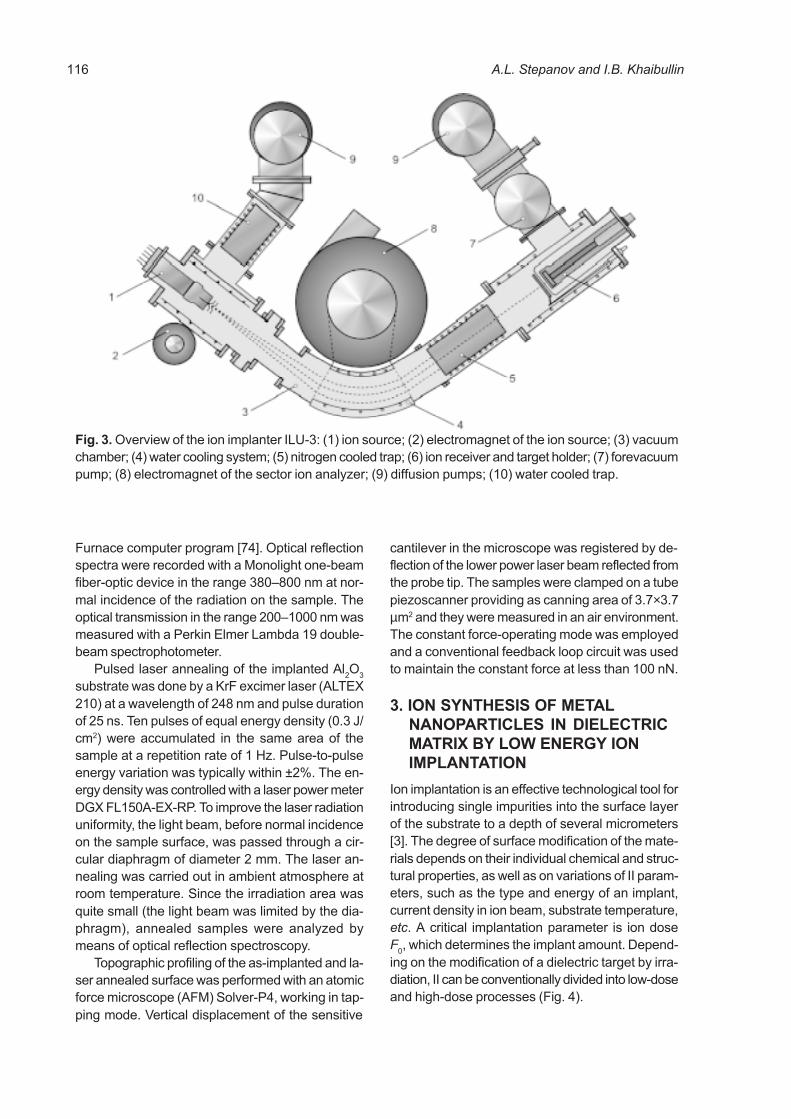
116 A.L. Stepanov and I.B. Khaibullin
Fig. 3. Overview of the ion implanter ILU-3: (1) ion source; (2) electromagnet of the ion source; (3) vacuumchamber; (4) water cooling system; (5) nitrogen cooled trap; (6) ion receiver and target holder; (7) forevacuumpump; (8) electromagnet of the sector ion analyzer; (9) diffusion pumps; (10) water cooled trap.
Furnace computer program [74]. Optical reflectionspectra were recorded with a Monolight one-beamfiber-optic device in the range 380�800 nm at nor-mal incidence of the radiation on the sample. Theoptical transmission in the range 200�1000 nm wasmeasured with a Perkin Elmer Lambda 19 double-beam spectrophotometer.
Pulsed laser annealing of the implanted Al2O
3
substrate was done by a KrF excimer laser (ALTEX210) at a wavelength of 248 nm and pulse durationof 25 ns. Ten pulses of equal energy density (0.3 J/cm2) were accumulated in the same area of thesample at a repetition rate of 1 Hz. Pulse-to-pulseenergy variation was typically within ±2%. The en-ergy density was controlled with a laser power meterDGX FL150A-EX-RP. To improve the laser radiationuniformity, the light beam, before normal incidenceon the sample surface, was passed through a cir-cular diaphragm of diameter 2 mm. The laser an-nealing was carried out in ambient atmosphere atroom temperature. Since the irradiation area wasquite small (the light beam was limited by the dia-phragm), annealed samples were analyzed bymeans of optical reflection spectroscopy.
Topographic profiling of the as-implanted and la-ser annealed surface was performed with an atomicforce microscope (AFM) Solver-P4, working in tap-ping mode. Vertical displacement of the sensitive
cantilever in the microscope was registered by de-flection of the lower power laser beam reflected fromthe probe tip. The samples were clamped on a tubepiezoscanner providing as canning area of 3.7×3.7µm2 and they were measured in an air environment.The constant force-operating mode was employedand a conventional feedback loop circuit was usedto maintain the constant force at less than 100 nN.
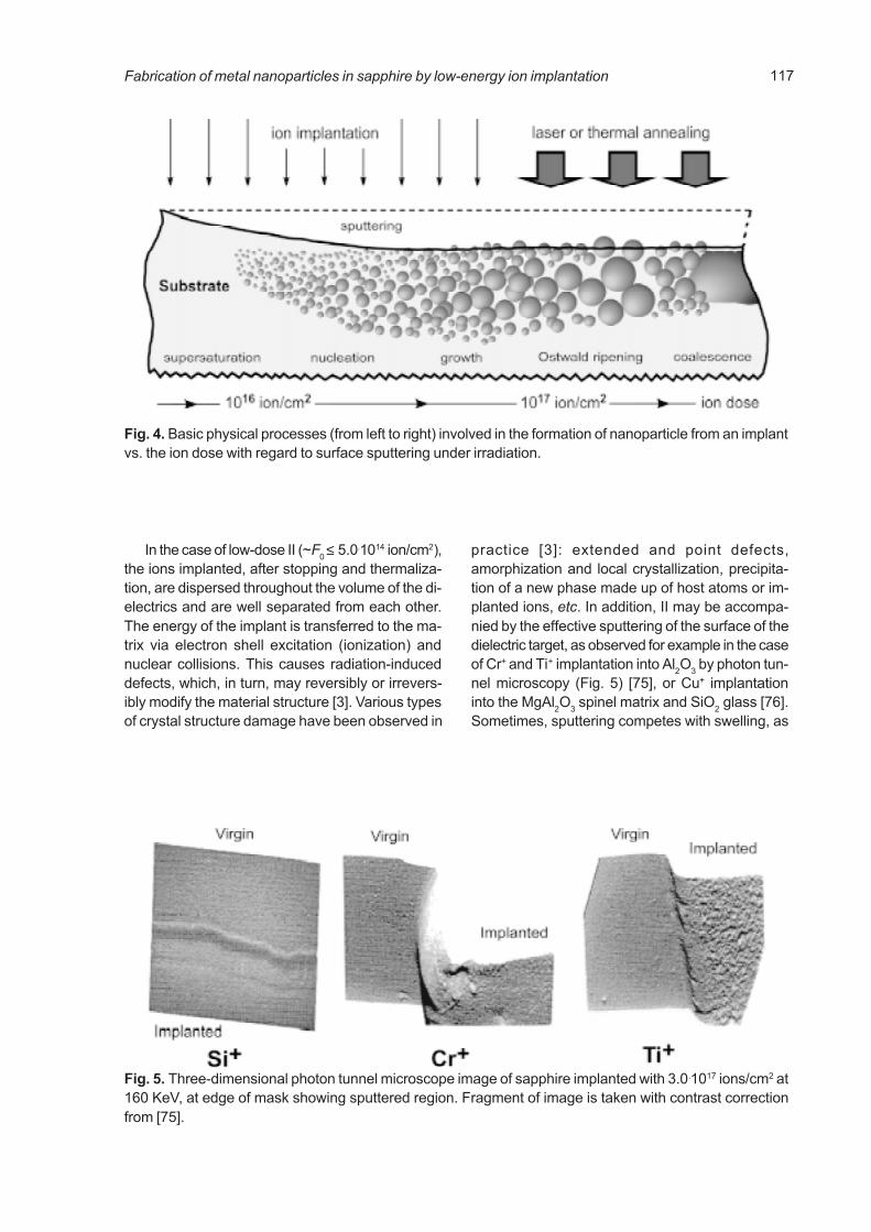
3. ION SYNTHESIS OF METALNANOPARTICLES IN DIELECTRICMATRIX BY LOW ENERGY IONIMPLANTATION
Ion implantation is an effective technological tool forintroducing single impurities into the surface layerof the substrate to a depth of several micrometers[3]. The degree of surface modification of the mate-rials depends on their individual chemical and struc-tural properties, as well as on variations of II param-eters, such as the type and energy of an implant,current density in ion beam, substrate temperature,etc. A critical implantation parameter is ion doseF
0, which determines the implant amount. Depend-
ing on the modification of a dielectric target by irra-diation, II can be conventionally divided into low-doseand high-dose processes (Fig. 4).
117Fabrication of metal nanoparticles in sapphire by low-energy ion implantation
Fig. 4. Basic physical processes (from left to right) involved in the formation of nanoparticle from an implantvs. the ion dose with regard to surface sputtering under irradiation.
Fig. 5. Three-dimensional photon tunnel microscope image of sapphire implanted with 3.0.1017 ions/cm2 at160 KeV, at edge of mask showing sputtered region. Fragment of image is taken with contrast correctionfrom [75].
In the case of low-dose II (~F0≤ 5.0.1014 ion/cm2),
the ions implanted, after stopping and thermaliza-tion, are dispersed throughout the volume of the di-electrics and are well separated from each other.The energy of the implant is transferred to the ma-trix via electron shell excitation (ionization) andnuclear collisions. This causes radiation-induceddefects, which, in turn, may reversibly or irrevers-ibly modify the material structure [3]. Various typesof crystal structure damage have been observed in
practice [3]: extended and point defects,amorphization and local crystallization, precipita-tion of a new phase made up of host atoms or im-planted ions, etc. In addition, II may be accompa-nied by the effective sputtering of the surface of thedielectric target, as observed for example in the caseof Cr+ and Ti+ implantation into Al
2O
3 by photon tun-
nel microscopy (Fig. 5) [75], or Cu+ implantationinto the MgAl
2O
3 spinel matrix and SiO
2 glass [76].
Sometimes, sputtering competes with swelling, as
118 A.L. Stepanov and I.B. Khaibullin
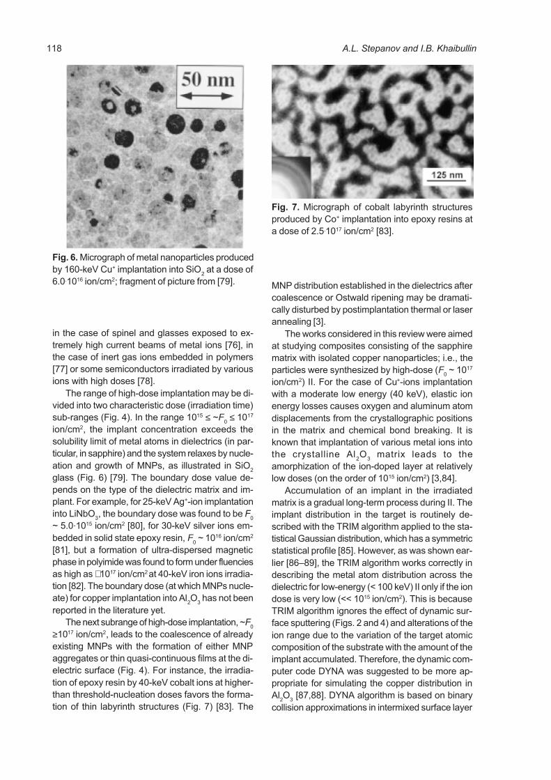
Fig. 6. Micrograph of metal nanoparticles producedby 160-keV Cu+ implantation into SiO
2 at a dose of
6.0.1016 ion/cm2; fragment of picture from [79].
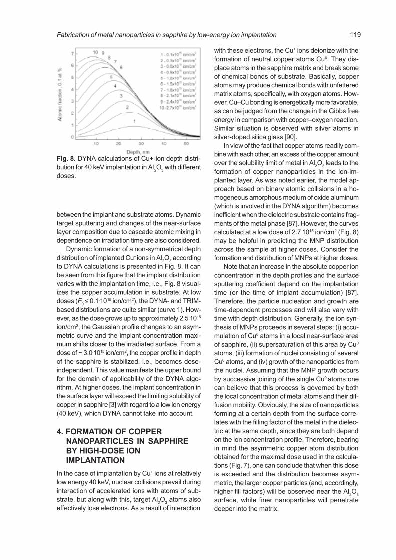
Fig. 7. Micrograph of cobalt labyrinth structuresproduced by Co+ implantation into epoxy resins ata dose of 2.5.1017 ion/cm2 [83].
in the case of spinel and glasses exposed to ex-tremely high current beams of metal ions [76], inthe case of inert gas ions embedded in polymers[77] or some semiconductors irradiated by variousions with high doses [78].
The range of high-dose implantation may be di-vided into two characteristic dose (irradiation time)sub-ranges (Fig. 4). In the range 1015 ≤ ~F
0 ≤ 1017
ion/cm2, the implant concentration exceeds thesolubility limit of metal atoms in dielectrics (in par-ticular, in sapphire) and the system relaxes by nucle-ation and growth of MNPs, as illustrated in SiO
2
glass (Fig. 6) [79]. The boundary dose value de-pends on the type of the dielectric matrix and im-plant. For example, for 25-keV Ag+-ion implantationinto LiNbO
3, the boundary dose was found to be F
0
~ 5.0.1015 ion/cm2 [80], for 30-keV silver ions em-bedded in solid state epoxy resin, F
0 ~ 1016 ion/cm2
[81], but a formation of ultra-dispersed magneticphase in polyimide was found to form under fluenciesas high as ∼1017 ion/cm2 at 40-keV iron ions irradia-tion [82]. The boundary dose (at which MNPs nucle-ate) for copper implantation into Al
2O
3 has not been
reported in the literature yet.The next subrange of high-dose implantation, ~F
0
≥1017 ion/cm2, leads to the coalescence of alreadyexisting MNPs with the formation of either MNPaggregates or thin quasi-continuous films at the di-electric surface (Fig. 4). For instance, the irradia-tion of epoxy resin by 40-keV cobalt ions at higher-than threshold-nucleation doses favors the forma-tion of thin labyrinth structures (Fig. 7) [83]. The
MNP distribution established in the dielectrics aftercoalescence or Ostwald ripening may be dramati-cally disturbed by postimplantation thermal or laserannealing [3].
The works considered in this review were aimedat studying composites consisting of the sapphirematrix with isolated copper nanoparticles; i.e., theparticles were synthesized by high-dose (F
0 ~ 1017
ion/cm2) II. For the case of Cu+-ions implantationwith a moderate low energy (40 keV), elastic ionenergy losses causes oxygen and aluminum atomdisplacements from the crystallographic positionsin the matrix and chemical bond breaking. It isknown that implantation of various metal ions intothe crystalline Al
2O
3 matrix leads to the
amorphization of the ion-doped layer at relativelylow doses (on the order of 1015 ion/cm2) [3,84].
Accumulation of an implant in the irradiatedmatrix is a gradual long-term process during II. Theimplant distribution in the target is routinely de-scribed with the TRIM algorithm applied to the sta-tistical Gaussian distribution, which has a symmetricstatistical profile [85]. However, as was shown ear-lier [86�89], the TRIM algorithm works correctly indescribing the metal atom distribution across thedielectric for low-energy (< 100 keV) II only if the iondose is very low (<< 1015 ion/cm2). This is becauseTRIM algorithm ignores the effect of dynamic sur-face sputtering (Figs. 2 and 4) and alterations of theion range due to the variation of the target atomiccomposition of the substrate with the amount of theimplant accumulated. Therefore, the dynamic com-puter code DYNA was suggested to be more ap-propriate for simulating the copper distribution inAl
2O
3 [87,88]. DYNA algorithm is based on binary
collision approximations in intermixed surface layer
119Fabrication of metal nanoparticles in sapphire by low-energy ion implantation
between the implant and substrate atoms. Dynamictarget sputtering and changes of the near-surfacelayer composition due to cascade atomic mixing independence on irradiation time are also considered.
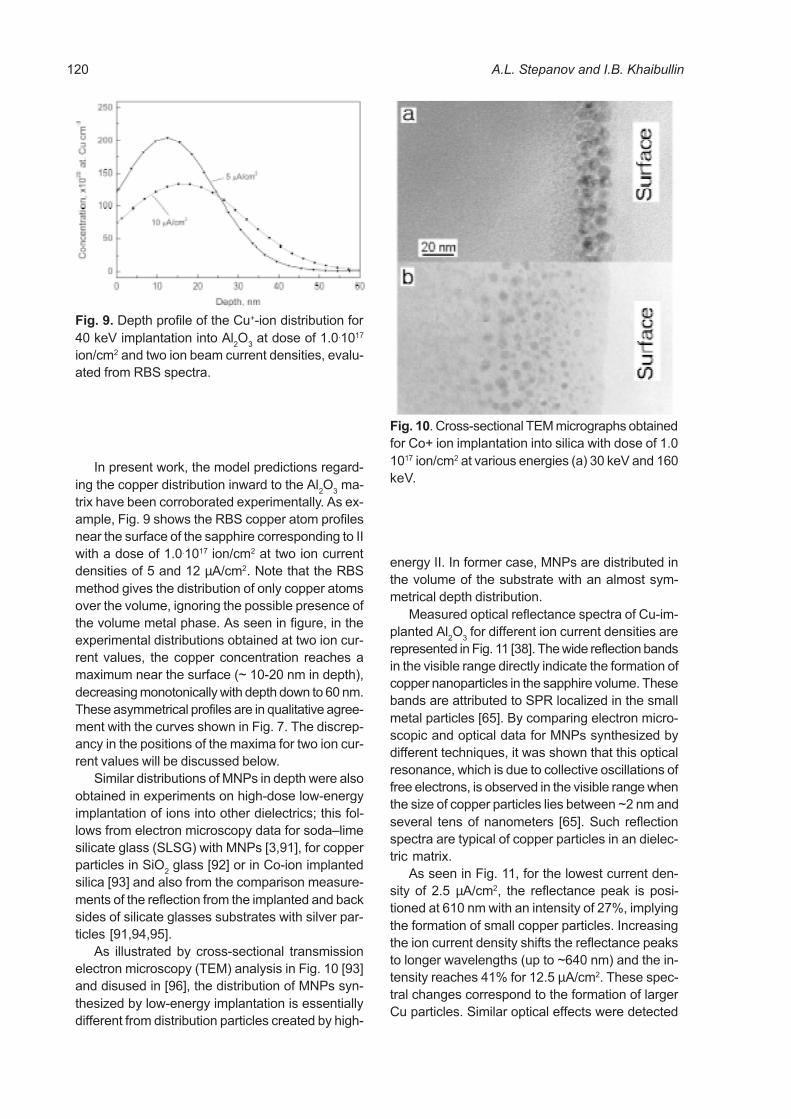
Dynamic formation of a non-symmetrical depthdistribution of implanted Cu+ ions in Al
2O
3 according
to DYNA calculations is presented in Fig. 8. It canbe seen from this figure that the implant distributionvaries with the implantation time, i.e., Fig. 8 visual-izes the copper accumulation in substrate. At lowdoses (F
0 ≤ 0.1.1015 ion/cm2), the DYNA- and TRIM-
based distributions are quite similar (curve 1). How-ever, as the dose grows up to approximately 2.5.1015
ion/cm2, the Gaussian profile changes to an asym-metric curve and the implant concentration maxi-mum shifts closer to the irradiated surface. From adose of ~ 3.0.1015 ion/cm2, the copper profile in depthof the sapphire is stabilized, i.e., becomes dose-independent. This value manifests the upper boundfor the domain of applicability of the DYNA algo-rithm. At higher doses, the implant concentration inthe surface layer will exceed the limiting solubility ofcopper in sapphire [3] with regard to a low ion energy(40 keV), which DYNA cannot take into account.
4. FORMATION OF COPPERNANOPARTICLES IN SAPPHIREBY HIGH-DOSE IONIMPLANTATION
In the case of implantation by Cu+ ions at relativelylow energy 40 keV, nuclear collisions prevail duringinteraction of accelerated ions with atoms of sub-strate, but along with this, target Al
2O
3 atoms also
effectively lose electrons. As a result of interaction
Fig. 8. DYNA calculations of Cu+-ion depth distri-bution for 40 keV implantation in Al
2O
3 with different
doses.
with these electrons, the Cu+ ions deionize with theformation of neutral copper atoms Cu0. They dis-place atoms in the sapphire matrix and break someof chemical bonds of substrate. Basically, copperatoms may produce chemical bonds with unfetteredmatrix atoms, specifically, with oxygen atoms. How-ever, Cu�Cu bonding is energetically more favorable,as can be judged from the change in the Gibbs freeenergy in comparison with copper�oxygen reaction.Similar situation is observed with silver atoms insilver-doped silica glass [90].
In view of the fact that copper atoms readily com-bine with each other, an excess of the copper amountover the solubility limit of metal in Al
2O
3 leads to the
formation of copper nanoparticles in the ion-im-planted layer. As was noted earlier, the model ap-proach based on binary atomic collisions in a ho-mogeneous amorphous medium of oxide aluminum(which is involved in the DYNA algorithm) becomesinefficient when the dielectric substrate contains frag-ments of the metal phase [87]. However, the curvescalculated at a low dose of 2.7.1015 ion/cm2 (Fig. 8)may be helpful in predicting the MNP distributionacross the sample at higher doses. Consider theformation and distribution of MNPs at higher doses.
Note that an increase in the absolute copper ionconcentration in the depth profiles and the surfacesputtering coefficient depend on the implantationtime (or the time of implant accumulation) [87].Therefore, the particle nucleation and growth aretime-dependent processes and will also vary withtime with depth distribution. Generally, the ion syn-thesis of MNPs proceeds in several steps: (i) accu-mulation of Cu0 atoms in a local near-surface areaof sapphire, (ii) supersaturation of this area by Cu0
atoms, (iii) formation of nuclei consisting of severalCu0 atoms, and (iv) growth of the nanoparticles fromthe nuclei. Assuming that the MNP growth occursby successive joining of the single Cu0 atoms onecan believe that this process is governed by boththe local concentration of metal atoms and their dif-fusion mobility. Obviously, the size of nanoparticlesforming at a certain depth from the surface corre-lates with the filling factor of the metal in the dielec-tric at the same depth, since they are both dependon the ion concentration profile. Therefore, bearingin mind the asymmetric copper atom distributionobtained for the maximal dose used in the calcula-tions (Fig. 7), one can conclude that when this doseis exceeded and the distribution becomes asym-metric, the larger copper particles (and, accordingly,higher fill factors) will be observed near the Al
2O
3
surface, while finer nanoparticles will penetratedeeper into the matrix.
120 A.L. Stepanov and I.B. Khaibullin
Fig. 9. Depth profile of the Cu+-ion distribution for40 keV implantation into Al
2O
3 at dose of 1.0.1017
ion/cm2 and two ion beam current densities, evalu-ated from RBS spectra.
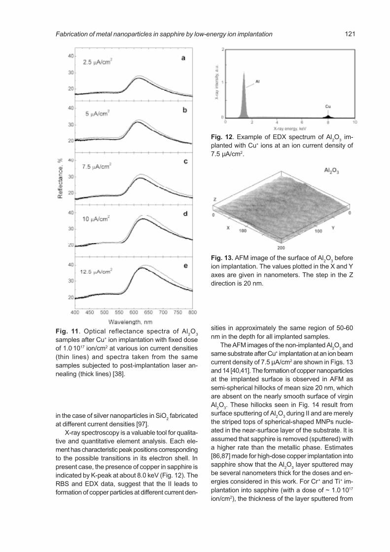
Fig. 10. Cross-sectional TEM micrographs obtainedfor Co+ ion implantation into silica with dose of 1.01017 ion/cm2 at various energies (a) 30 keV and 160keV.
In present work, the model predictions regard-ing the copper distribution inward to the Al
2O
3 ma-
trix have been corroborated experimentally. As ex-ample, Fig. 9 shows the RBS copper atom profilesnear the surface of the sapphire corresponding to IIwith a dose of 1.0.1017 ion/cm2 at two ion currentdensities of 5 and 12 µA/cm2. Note that the RBSmethod gives the distribution of only copper atomsover the volume, ignoring the possible presence ofthe volume metal phase. As seen in figure, in theexperimental distributions obtained at two ion cur-rent values, the copper concentration reaches amaximum near the surface (~ 10-20 nm in depth),decreasing monotonically with depth down to 60 nm.These asymmetrical profiles are in qualitative agree-ment with the curves shown in Fig. 7. The discrep-ancy in the positions of the maxima for two ion cur-rent values will be discussed below.
Similar distributions of MNPs in depth were alsoobtained in experiments on high-dose low-energyimplantation of ions into other dielectrics; this fol-lows from electron microscopy data for soda�limesilicate glass (SLSG) with MNPs [3,91], for copperparticles in SiO
2 glass [92] or in Co-ion implanted
silica [93] and also from the comparison measure-ments of the reflection from the implanted and backsides of silicate glasses substrates with silver par-ticles [91,94,95].
As illustrated by cross-sectional transmissionelectron microscopy (TEM) analysis in Fig. 10 [93]and disused in [96], the distribution of MNPs syn-thesized by low-energy implantation is essentiallydifferent from distribution particles created by high-
energy II. In former case, MNPs are distributed inthe volume of the substrate with an almost sym-metrical depth distribution.
Measured optical reflectance spectra of Cu-im-planted Al
2O
3 for different ion current densities are
represented in Fig. 11 [38]. The wide reflection bandsin the visible range directly indicate the formation ofcopper nanoparticles in the sapphire volume. Thesebands are attributed to SPR localized in the smallmetal particles [65]. By comparing electron micro-scopic and optical data for MNPs synthesized bydifferent techniques, it was shown that this opticalresonance, which is due to collective oscillations offree electrons, is observed in the visible range whenthe size of copper particles lies between ~2 nm andseveral tens of nanometers [65]. Such reflectionspectra are typical of copper particles in an dielec-tric matrix.
As seen in Fig. 11, for the lowest current den-sity of 2.5 µA/cm2, the reflectance peak is posi-tioned at 610 nm with an intensity of 27%, implyingthe formation of small copper particles. Increasingthe ion current density shifts the reflectance peaksto longer wavelengths (up to ~640 nm) and the in-tensity reaches 41% for 12.5 µA/cm2. These spec-tral changes correspond to the formation of largerCu particles. Similar optical effects were detected
121Fabrication of metal nanoparticles in sapphire by low-energy ion implantation
Fig. 11. Optical reflectance spectra of Al2O
3
samples after Cu+ ion implantation with fixed doseof 1.0.1017 ion/cm2 at various ion current densities(thin lines) and spectra taken from the samesamples subjected to post-implantation laser an-nealing (thick lines) [38].
in the case of silver nanoparticles in SiO2 fabricated
at different current densities [97].X-ray spectroscopy is a valuable tool for qualita-
tive and quantitative element analysis. Each ele-ment has characteristic peak positions correspondingto the possible transitions in its electron shell. Inpresent case, the presence of copper in sapphire isindicated by K-peak at about 8.0 keV (Fig. 12). TheRBS and EDX data, suggest that the II leads toformation of copper particles at different current den-
Fig. 12. Example of EDX spectrum of Al2O
3 im-
planted with Cu+ ions at an ion current density of7.5 µA/cm2.
Fig. 13. AFM image of the surface of Al2O
3 before
ion implantation. The values plotted in the X and Yaxes are given in nanometers. The step in the Zdirection is 20 nm.
sities in approximately the same region of 50-60nm in the depth for all implanted samples.
The AFM images of the non-implanted Al2O
3 and
same substrate after Cu+ implantation at an ion beamcurrent density of 7.5 µA/cm2 are shown in Figs. 13and 14 [40,41]. The formation of copper nanoparticlesat the implanted surface is observed in AFM assemi-spherical hillocks of mean size 20 nm, whichare absent on the nearly smooth surface of virginAl
2O
3. These hillocks seen in Fig. 14 result from
surface sputtering of Al2O
3 during II and are merely
the striped tops of spherical-shaped MNPs nucle-ated in the near-surface layer of the substrate. It isassumed that sapphire is removed (sputtered) witha higher rate than the metallic phase. Estimates[86,87] made for high-dose copper implantation intosapphire show that the Al
2O
3 layer sputtered may
be several nanometers thick for the doses and en-ergies considered in this work. For Cr+ and Ti+ im-plantation into sapphire (with a dose of ~ 1.0.1017
ion/cm2), the thickness of the layer sputtered from
122 A.L. Stepanov and I.B. Khaibullin
Fig. 14. AFM image of a fragment of the surface of Al2O
3 implanted with Cu+ ions at an ion current density
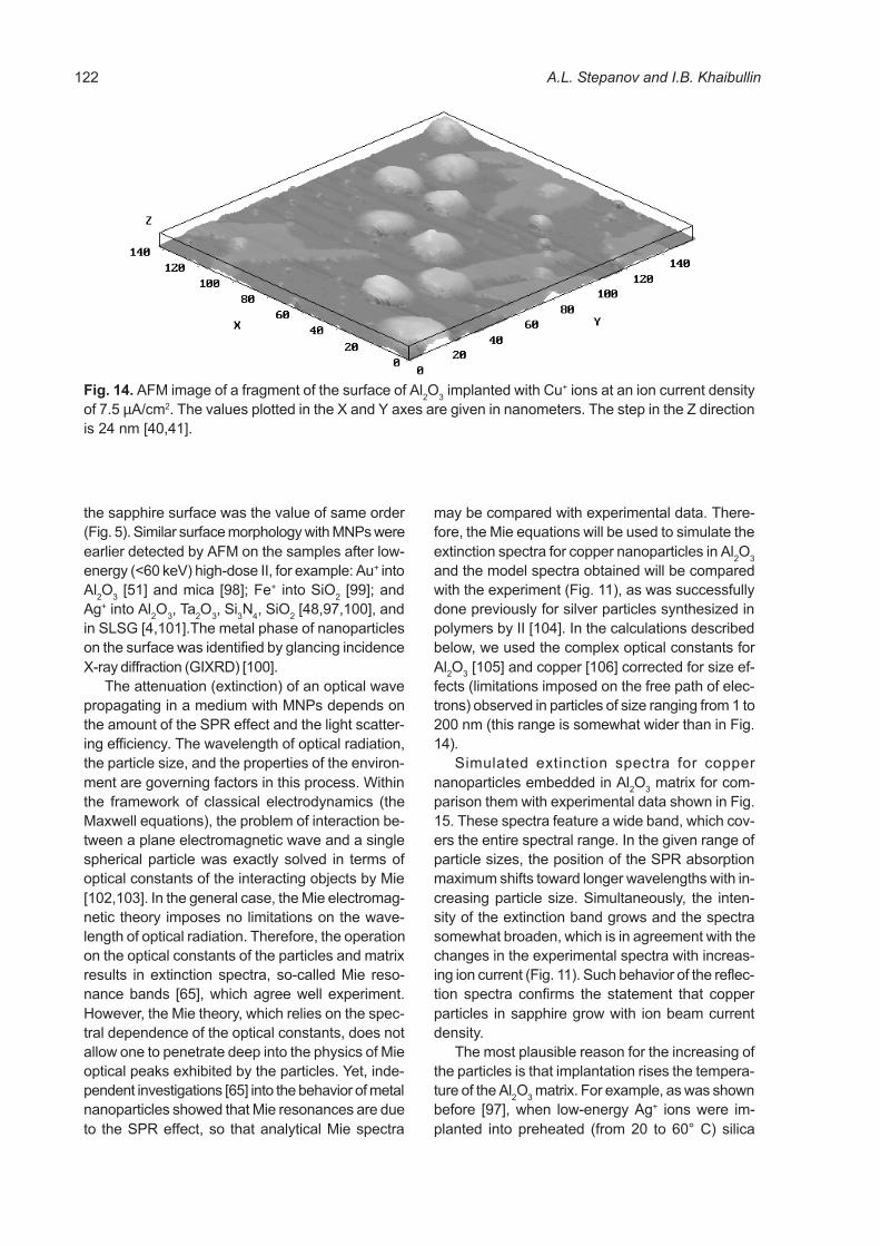
of 7.5 µA/cm2. The values plotted in the X and Y axes are given in nanometers. The step in the Z directionis 24 nm [40,41].
the sapphire surface was the value of same order(Fig. 5). Similar surface morphology with MNPs wereearlier detected by AFM on the samples after low-energy (<60 keV) high-dose II, for example: Au+ intoAl
2O
3 [51] and mica [98]; Fe+ into SiO
2 [99]; and
Ag+ into Al2O
3, Ta
2O
3, Si
3N
4, SiO
2 [48,97,100], and
in SLSG [4,101].The metal phase of nanoparticleson the surface was identified by glancing incidenceX-ray diffraction (GIXRD) [100].
The attenuation (extinction) of an optical wavepropagating in a medium with MNPs depends onthe amount of the SPR effect and the light scatter-ing efficiency. The wavelength of optical radiation,the particle size, and the properties of the environ-ment are governing factors in this process. Withinthe framework of classical electrodynamics (theMaxwell equations), the problem of interaction be-tween a plane electromagnetic wave and a singlespherical particle was exactly solved in terms ofoptical constants of the interacting objects by Mie[102,103]. In the general case, the Mie electromag-netic theory imposes no limitations on the wave-length of optical radiation. Therefore, the operationon the optical constants of the particles and matrixresults in extinction spectra, so-called Mie reso-nance bands [65], which agree well experiment.However, the Mie theory, which relies on the spec-tral dependence of the optical constants, does notallow one to penetrate deep into the physics of Mieoptical peaks exhibited by the particles. Yet, inde-pendent investigations [65] into the behavior of metalnanoparticles showed that Mie resonances are dueto the SPR effect, so that analytical Mie spectra
may be compared with experimental data. There-fore, the Mie equations will be used to simulate theextinction spectra for copper nanoparticles in Al
2O
3
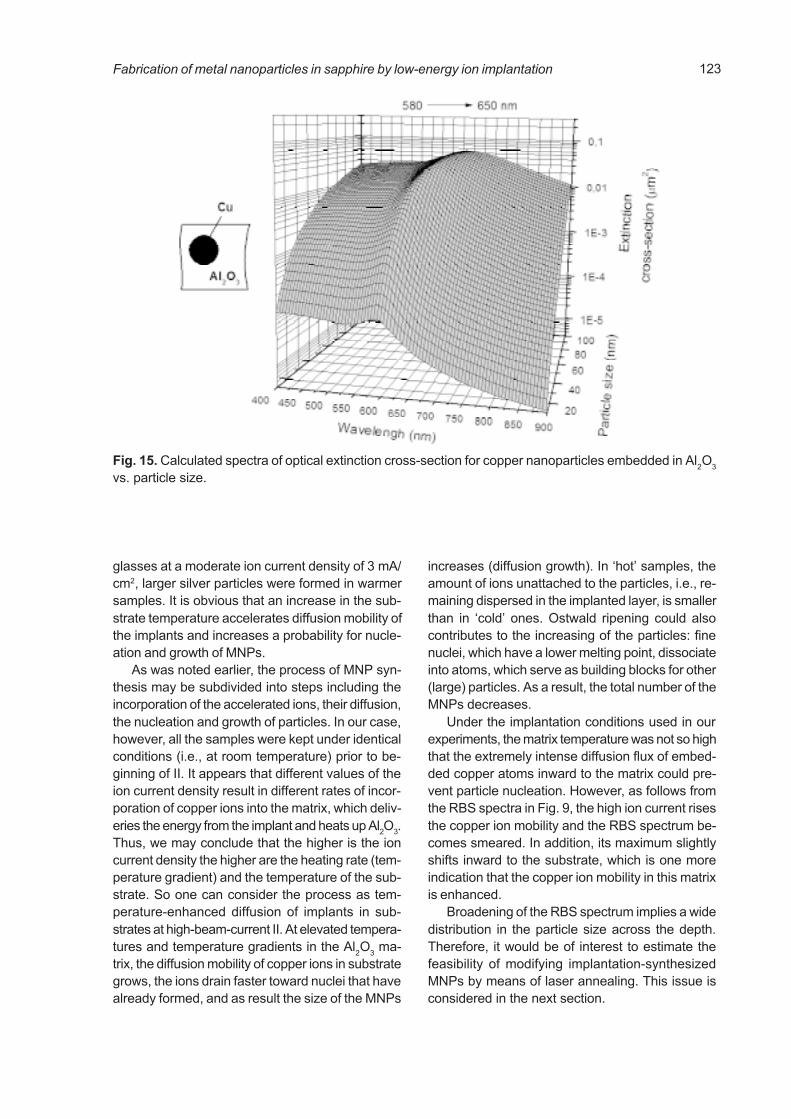
and the model spectra obtained will be comparedwith the experiment (Fig. 11), as was successfullydone previously for silver particles synthesized inpolymers by II [104]. In the calculations describedbelow, we used the complex optical constants forAl2O3 [105] and copper [106] corrected for size ef-fects (limitations imposed on the free path of elec-trons) observed in particles of size ranging from 1 to200 nm (this range is somewhat wider than in Fig.14).
Simulated extinction spectra for coppernanoparticles embedded in Al2O3 matrix for com-parison them with experimental data shown in Fig.15. These spectra feature a wide band, which cov-ers the entire spectral range. In the given range ofparticle sizes, the position of the SPR absorptionmaximum shifts toward longer wavelengths with in-creasing particle size. Simultaneously, the inten-sity of the extinction band grows and the spectrasomewhat broaden, which is in agreement with thechanges in the experimental spectra with increas-ing ion current (Fig. 11). Such behavior of the reflec-tion spectra confirms the statement that copperparticles in sapphire grow with ion beam currentdensity.
The most plausible reason for the increasing ofthe particles is that implantation rises the tempera-ture of the Al
2O
3 matrix. For example, as was shown
before [97], when low-energy Ag+ ions were im-planted into preheated (from 20 to 60° C) silica
123Fabrication of metal nanoparticles in sapphire by low-energy ion implantation
Fig. 15. Calculated spectra of optical extinction cross-section for copper nanoparticles embedded in Al2O
3
vs. particle size.
glasses at a moderate ion current density of 3 mA/cm2, larger silver particles were formed in warmersamples. It is obvious that an increase in the sub-strate temperature accelerates diffusion mobility ofthe implants and increases a probability for nucle-ation and growth of MNPs.
As was noted earlier, the process of MNP syn-thesis may be subdivided into steps including theincorporation of the accelerated ions, their diffusion,the nucleation and growth of particles. In our case,however, all the samples were kept under identicalconditions (i.e., at room temperature) prior to be-ginning of II. It appears that different values of theion current density result in different rates of incor-poration of copper ions into the matrix, which deliv-eries the energy from the implant and heats up Al2O3.Thus, we may conclude that the higher is the ioncurrent density the higher are the heating rate (tem-perature gradient) and the temperature of the sub-strate. So one can consider the process as tem-perature-enhanced diffusion of implants in sub-strates at high-beam-current II. At elevated tempera-tures and temperature gradients in the Al
2O
3 ma-
trix, the diffusion mobility of copper ions in substrategrows, the ions drain faster toward nuclei that havealready formed, and as result the size of the MNPs
increases (diffusion growth). In �hot� samples, theamount of ions unattached to the particles, i.e., re-maining dispersed in the implanted layer, is smallerthan in �cold� ones. Ostwald ripening could alsocontributes to the increasing of the particles: finenuclei, which have a lower melting point, dissociateinto atoms, which serve as building blocks for other(large) particles. As a result, the total number of theMNPs decreases.
Under the implantation conditions used in ourexperiments, the matrix temperature was not so highthat the extremely intense diffusion flux of embed-ded copper atoms inward to the matrix could pre-vent particle nucleation. However, as follows fromthe RBS spectra in Fig. 9, the high ion current risesthe copper ion mobility and the RBS spectrum be-comes smeared. In addition, its maximum slightlyshifts inward to the substrate, which is one moreindication that the copper ion mobility in this matrixis enhanced.
Broadening of the RBS spectrum implies a widedistribution in the particle size across the depth.Therefore, it would be of interest to estimate thefeasibility of modifying implantation-synthesizedMNPs by means of laser annealing. This issue isconsidered in the next section.
124 A.L. Stepanov and I.B. Khaibullin
5. MODIFICATION OF METALNANOPARTICLES IN SAPPHIREBY LASER ANNEALING
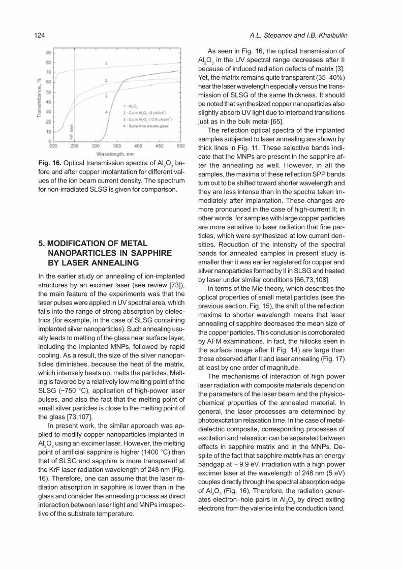
In the earlier study on annealing of ion-implantedstructures by an excimer laser (see review [73]),the main feature of the experiments was that thelaser pulses were applied in UV spectral area, whichfalls into the range of strong absorption by dielec-trics (for example, in the case of SLSG containingimplanted silver nanoparticles). Such annealing usu-ally leads to melting of the glass near surface layer,including the implanted MNPs, followed by rapidcooling. As a result, the size of the silver nanopar-ticles diminishes, because the heat of the matrix,which intensely heats up, melts the particles. Melt-ing is favored by a relatively low melting point of theSLSG (~750 °C), application of high-power laserpulses, and also the fact that the melting point ofsmall silver particles is close to the melting point ofthe glass [73,107].
In present work, the similar approach was ap-plied to modify copper nanoparticles implanted inAl2O3 using an excimer laser. However, the meltingpoint of artificial sapphire is higher (1400 °C) thanthat of SLSG and sapphire is more transparent atthe KrF laser radiation wavelength of 248 nm (Fig.16). Therefore, one can assume that the laser ra-diation absorption in sapphire is lower than in theglass and consider the annealing process as directinteraction between laser light and MNPs irrespec-tive of the substrate temperature.
Fig. 16. Optical transmission spectra of Al2O
3 be-
fore and after copper implantation for different val-ues of the ion beam current density. The spectrumfor non-irradiated SLSG is given for comparison.
As seen in Fig. 16, the optical transmission ofAl
2O
3 in the UV spectral range decreases after II
because of induced radiation defects of matrix [3].Yet, the matrix remains quite transparent (35�40%)near the laser wavelength especially versus the trans-mission of SLSG of the same thickness. It shouldbe noted that synthesized copper nanoparticles alsoslightly absorb UV light due to interband transitionsjust as in the bulk metal [65].
The reflection optical spectra of the implantedsamples subjected to laser annealing are shown bythick lines in Fig. 11. These selective bands indi-cate that the MNPs are present in the sapphire af-ter the annealing as well. However, in all thesamples, the maxima of these reflection SPP bandsturn out to be shifted toward shorter wavelength andthey are less intense than in the spectra taken im-mediately after implantation. These changes aremore pronounced in the case of high-current II; inother words, for samples with large copper particlesare more sensitive to laser radiation that fine par-ticles, which were synthesized at low current den-sities. Reduction of the intensity of the spectralbands for annealed samples in present study issmaller than it was earlier registered for copper andsilver nanoparticles formed by II in SLSG and treatedby laser under similar conditions [66,73,108].
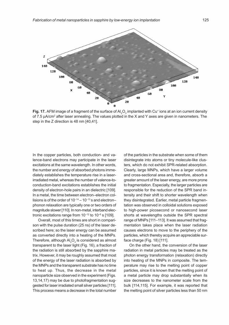
In terms of the Mie theory, which describes theoptical properties of small metal particles (see theprevious section, Fig. 15), the shift of the reflectionmaxima to shorter wavelength means that laserannealing of sapphire decreases the mean size ofthe copper particles. This conclusion is corroboratedby AFM examinations. In fact, the hillocks seen inthe surface image after II Fig. 14) are large thanthose observed after II and laser annealing (Fig. 17)at least by one order of magnitude.
The mechanisms of interaction of high powerlaser radiation with composite materials depend onthe parameters of the laser beam and the physico-chemical properties of the annealed material. Ingeneral, the laser processes are determined byphotoexcitation relaxation time. In the case of metal-dielectric composite, corresponding processes ofexcitation and relaxation can be separated betweeneffects in sapphire matrix and in the MNPs. De-spite of the fact that sapphire matrix has an energybandgap at ~ 9.9 eV, irradiation with a high powerexcimer laser at the wavelength of 248 nm (5 eV)couples directly through the spectral absorption edgeof Al
2O
3 (Fig. 16), Therefore, the radiation gener-
ates electron�hole pairs in Al2O
3 by direct exiting
electrons from the valence into the conduction band.
125Fabrication of metal nanoparticles in sapphire by low-energy ion implantation
In the copper particles, both conduction- and va-lence-band electrons may participate in the laserexcitations at the same wavelength. In other words,the number and energy of absorbed photons imme-diately establishes the temperature rise in a laser-irradiated metal, whereas the number of valence-to-conduction-band excitations establishes the initialdensity of electron-hole pairs in an dielectric [109].In a metal, the time between electron�electron col-lisions is of the order of 10�14 � 10�13 s and electron�phonon relaxation are typically one or two orders ofmagnitude slower [110]. In non-metal, interband elec-tronic excitations range from 10�12 to 10�6 s [109].
Overall, most of this times are short in compari-son with the pulse duration (25 ns) of the laser de-scribed here; so the laser energy can be assumedas converted directly into a heating of the MNPs.Therefore, although Al
2O
3 is considered as almost
transparent to the laser light (Fig. 16), a fraction ofthe radiation is still absorbed by the sapphire ma-trix. However, it may be roughly assumed that mostof the energy of the laser radiation is absorbed bythe MNPs and the transparent substrate has no timeto heat up. Thus, the decrease in the metalnanoparticle size observed in the experiment (Figs.13,14,17) may be due to photofragmentation sug-gested for laser irradiated small silver particles [111].This process means a decrease in the total number
Fig. 17. AFM image of a fragment of the surface of Al2O
3 implanted with Cu+ ions at an ion current density
of 7.5 µA/cm2 after laser annealing. The values plotted in the X and Y axes are given in nanometers. Thestep in the Z direction is 48 nm [40,41].
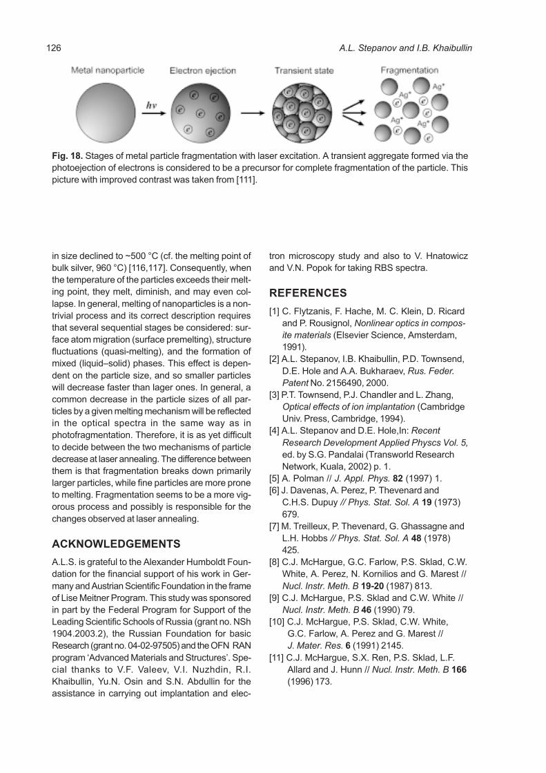
of the particles in the substrate when some of themdisintegrate into atoms or tiny molecule-like clus-ters, which do not exhibit SPR-related absorption.Clearly, large MNPs, which have a larger volumeand cross-sectional area and, therefore, absorb agreater amount of the laser energy, are more proneto fragmentation. Especially, the larger particles areresponsible for the reduction of the SPR band in-tensity and their shift to shorter wavelength whenthey disintegrated. Earlier, metal particle fragmen-tation was observed in colloidal solutions exposedto high-power picosecond or nanosecond lasershorts at wavelengths outside the SPR spectralrange of MNPs [111�113]. It was assumed that frag-mentation takes place when the laser radiationcauses electrons to move to the periphery of theparticles, which thereby acquire an appreciable sur-face charge (Fig. 18) [111].
On the other hand, the conversion of the laserradiation in metal particles may be treated as thephoton energy transformation (relaxation) directlyinto heating of the MNPs in composite. The tem-perature may rise to the melting point of copperparticles, since it is known that the melting point ofa metal particle may drop substantially when itssize decreases to the nanometer scale from thebulk [114,115]. For example, it was reported thatthe melting point of silver particles less than 50 nm
126 A.L. Stepanov and I.B. Khaibullin
in size declined to ~500 °C (cf. the melting point ofbulk silver, 960 °C) [116,117]. Consequently, whenthe temperature of the particles exceeds their melt-ing point, they melt, diminish, and may even col-lapse. In general, melting of nanoparticles is a non-trivial process and its correct description requiresthat several sequential stages be considered: sur-face atom migration (surface premelting), structurefluctuations (quasi-melting), and the formation ofmixed (liquid�solid) phases. This effect is depen-dent on the particle size, and so smaller particleswill decrease faster than lager ones. In general, acommon decrease in the particle sizes of all par-ticles by a given melting mechanism will be reflectedin the optical spectra in the same way as inphotofragmentation. Therefore, it is as yet difficultto decide between the two mechanisms of particledecrease at laser annealing. The difference betweenthem is that fragmentation breaks down primarilylarger particles, while fine particles are more proneto melting. Fragmentation seems to be a more vig-orous process and possibly is responsible for thechanges observed at laser annealing.
ACKNOWLEDGEMENTS
A.L.S. is grateful to the Alexander Humboldt Foun-dation for the financial support of his work in Ger-many and Austrian Scientific Foundation in the frameof Lise Meitner Program. This study was sponsoredin part by the Federal Program for Support of theLeading Scientific Schools of Russia (grant no. NSh1904.2003.2), the Russian Foundation for basicResearch (grant no. 04-02-97505) and the OFN RANprogram �Advanced Materials and Structures�. Spe-cial thanks to V.F. Valeev, V.I. Nuzhdin, R.I.Khaibullin, Yu.N. Osin and S.N. Abdullin for theassistance in carrying out implantation and elec-
Fig. 18. Stages of metal particle fragmentation with laser excitation. A transient aggregate formed via thephotoejection of electrons is considered to be a precursor for complete fragmentation of the particle. Thispicture with improved contrast was taken from [111].
tron microscopy study and also to V. Hnatowiczand V.N. Popok for taking RBS spectra.
REFERENCES
[1] C. Flytzanis, F. Hache, M. C. Klein, D. Ricardand P. Rousignol, Nonlinear optics in compos-ite materials (Elsevier Science, Amsterdam,1991).
[2] A.L. Stepanov, I.B. Khaibullin, P.D. Townsend,D.E. Hole and A.A. Bukharaev, Rus. Feder.Patent No. 2156490, 2000.
[3] P.T. Townsend, P.J. Chandler and L. Zhang,Optical effects of ion implantation (CambridgeUniv. Press, Cambridge, 1994).
[4] A.L. Stepanov and D.E. Hole,In: RecentResearch Development Applied Physcs Vol. 5,ed. by S.G. Pandalai (Transworld ResearchNetwork, Kuala, 2002) p. 1.
[5] A. Polman // J. Appl. Phys. 82 (1997) 1.[6] J. Davenas, A. Perez, P. Thevenard and
C.H.S. Dupuy // Phys. Stat. Sol. A 19 (1973)679.
[7] M. Treilleux, P. Thevenard, G. Ghassagne andL.H. Hobbs // Phys. Stat. Sol. A 48 (1978)425.
[8] C.J. McHargue, G.C. Farlow, P.S. Sklad, C.W.White, A. Perez, N. Kornilios and G. Marest //Nucl. Instr. Meth. B 19-20 (1987) 813.
[9] C.J. McHargue, P.S. Sklad and C.W. White //Nucl. Instr. Meth. B 46 (1990) 79.
[10] C.J. McHargue, P.S. Sklad, C.W. White,G.C. Farlow, A. Perez and G. Marest //J. Mater. Res. 6 (1991) 2145.
[11] C.J. McHargue, S.X. Ren, P.S. Sklad, L.F.Allard and J. Hunn // Nucl. Instr. Meth. B 166(1996) 173.
127Fabrication of metal nanoparticles in sapphire by low-energy ion implantation
[12] C.J. McHargue, S.X. Ren and J.D. Hunn //Mat. Sci. Eng. A 253 (1998) 1.
[13] M. Ohkubo, T. Hioki and J. Kawamoto //J. Appl. Phys. 62 (1987) 3069.
[14] M. Ohkubo, T. Hioki, N. Suzuki, T. Ishiguroand J. Kawamoto // Nucl. Instr. Meth. B 39(1989) 675.
[15] G.C .Farlow, P.S. Sklad, C.W. White andC.J. McHargue // J. Mater. Res. 5 (1990)1502.
[16] C. Donnet, G. Marest, N. Moncoffre,J. Tousset, A. Rahioui and C. Esnouf // Nucl.Instr. Meth. B 59-60 (1991) 1205.
[17] P.S. Sklad, C.J. McHargue, C.W. White andG.C. Farlow // J. Mat. Sci. 27 (1992) 5895.
[18] H.-G. Jang, H.-B. Kim, J.-H. Joo, C.-N.Whang, H.-K. Kim, D.-W. Moon, J.J. Wooand S.-O. Kim // Nucl. Instr. Meth. B 124(1997) 528.
[19] T. Kobayashi and T. Terai // Nucl. Instr. Meth.B 141 (1998) 441.
[20] T. Kobayashi, A. Nakanishi, K .Fukumuraand G. Langouche // J. Appl. Phys. 83 (1998)4631.
[21] I. Sakamoto, S. Honda, H. Tanoue,N. Hayashi and H. Yamane // Nucl. Instr.Meth. B 148 (1999) 1039.
[22] N. Hayashi, T. Toriyama, H. Wakabayashi,I. Sakamoto, T. Okada and K. Kuriyama //Nucl. Instr. Meth. B 158-159 (2002) 193.
[23] H. Wakabayashi, T. Hirai, T. Toriyama,N. Hayashi and I. Sakamoto // Phys. Stat.Sol. 189 (2002) 515.
[24] E. Alves, C. MacHargue, R.C. da Silva,C. Jesus, O. Conde, M.F. da Silva and J.C.Soares // Surf. Coat.. Tech. 128-129 (2002)434.
[25] T. Monteiro, C. Boemare, M.J. Soares,E. Alves, C. Marques, C. McHargue, L.C.Ononye and L.F. Allard // Nucl. Instr. Meth. B191 (2002) 638.
[26] C.W. White, S.P. Withrow, K.D. Sorge,A. Meldrum, J.D. Budai, J.R. Thompson andL.A. Boatner // J. Appl. Phys. 93 (2003)5656.
[27] C.J. McHargue, L.C. Ononye, E. Alves,C. Marques and L.F. Allard // Nucl. Instr.Meth. B 218 (2004) 227.
[28] Y. Saito, H. Horie and S. Suganomata //Nucl. Instr. Meth. B 59-60 (1991) 1173.
[29] C. Marques, M.M. Cruz, R.C. da Silva andE. Alves // Nucl. Instr. Meth. B 175-177(2001) 500.
[30] C. Marques, M.M. Cruz, R.C. da Silva andE. Alves // Surf. Coat. Tech. 158-159 (2002)54.
[31] A. Meldrum, L.A. Boatner and K. Sorge //Nucl. Instr. Meth. B 207 (2003) 36.
[32] T. Kobayashi, T. Terai, T. Yoneoka andS. Tanaka // Nucl. Instr. Meth. B 116 (1996)187.
[33] X. Xiang, X.T. Zu, S. Zhu and L.M. Wang //Appl. Phys. Lett. 84 (2004) 52.
[34] X. Xiang, X.T. Zu, S. Zhu and L.M. Wang //Mat. Res. Soc. Symp. Proc. 792 (2004)R9.9.1.
[35] D. Ila, E.K. Williams, S. Sarkisov, D.B.Pocker, D.K. Hensley, C. Klatt andS. Kalbitzer // Mat. Res. Soc. Symp. Proc.504 (1998) 381.
[36] M. Ikeyama, S. Nakao, M. Tazawa,K. Kadono and K. Kamada // Nucl. Instr.Meth. B 175-177 (2001) 652.
[37] M. Ikeyama, S .Nakao and M. Tazawa //Surf. Coat. Tech. 158-159 (2002) 720.
[38] A.L. Stepanov, U. Kreibig, D.E. Hole, R.I.Khaibullin, I.B. Khaibullin and V.N. Popok //Nucl. Instr. Meth. B 178 (2001) 120.
[39] A.L. Stepanov // Tech. Phys. Lett. 28 (2002)864.
[40] A.L. Stepanov, V.N. Popok, D.E. Hole andI.B. Khaibullin // Appl. Phys. A 74 (2002)441.
[41] A.L. Stepanov and V.N. Popok // AIP Conf.Proc. 680 (2003) 601.
[42] A.L. Stepanov // Tech. Phys. (2005) in press.[43] G. Battaglin, R. Bertoncello, M. Casarin,
E. Cattaruzza, G. Mattei, P. Mazzoldi,F. Trivillin and M. Urbani // J. Non.-Cryst.Solids 253 (1999) 251.
[44] M. Rahmani; L.H. Abu-Hassan, P.D.Townsend, I.H. Wilson and G.L. Destefanis //Nucl. Instr. Meth. B 32 (1988) 56.
[45] M. Rahmani and P.D. Townsend // Vacuum39 (1989) 1157.
[46] C.W. White, D.K. Thomas, R.A Zuhr, J.C.McXallum, A. Pogany, R.H. haglund, R.H.Magruder III and L. Yang // Mater. Res. Soc.Proc. 258 (1992) 331.
[47] C.W. White, D.K. Thomas, D.K. Hensley,R.A. Zuhr, J.C. McCallum, A. Pogany, R.F.Haglund, R.H. Magruder and L. Yang //Nanostrust. Mat. 3 (1993) 447.
[48] G. Steiner, M.T. Pham, C. Kuhne andR. Salzer // Fresenius J. Anal. Chem. 362(1998) 9.
128 A.L. Stepanov and I.B. Khaibullin
[49] E. Alves, R.C. da Silva, O. Conde, M.F. daSilva and J.C. Soares // Nucl. Instr. Meth. B148 (1999) 1049.
[50] M. Ohkubo and N. Suzuki // Phil. Mag. Lett.57 (1988) 261.
[51] D.O. Henderson, R. Mu, M.A. George,A. Burger, S.H. Morgan, C.W. White, R.A.Zuhr and R.H. Magruder III // J. Vac. Sci.Technol. B 13 (1995) 1198.
[52] C. Marques, E. Alves, R.C. da Silva, M.R.Silva and A.L. Stepanov // Nucl. Instr. Meth.B 218 (2004) 139.
[53] S. Dhara, B. Sundaravel, T.R. Ravindrn,K.G.M. Nair, C. David, B.K. Panigrahi,P. Magudapathy and K.H. Chen // Chem.Phys. Lett. 399 (2004) 354.
[54] N. Can, P.D. Townsend and D.E. Hole //Appl. Phys. Lett. 65 (1994) 1871.
[55] N. Can, P.D. Townsend, D.E. Hole, H.V.Snelling, J.M. Ballesteros and C.N. Afonso //J. Appl. Phys. 78 (1995) 6737.
[56] N. Hayashi, I. Sakamoto, H. Wakabayashi,T. Toriyama and S. Honda // J. Appl. Phys.94 (2003) 2597.
[57] C.E. Vallet, C.W. White, S.P. Withrow, J.D.Budai, L.A. Boatner, K.D. Sorge, J.R.Thompson, K.S. Beaty and A. Meldrum //J. Appl. Phys. 92 (2002) 6200.
[58] C.W. White, S.P. Withrow, J.D. Budai, L.A.Boatner, K.D. Sorge, J.R. Thompson, K.S.Beaty and A. Meldrum // Nucl. Instr. Meth. B191 (2002) 437.
[59] S.P. Withrow, C.W. White, J.D. Budai, L.A.Boatner, K.D. Sorge, J.R. Thompson andR. Kalyanaraman // J. Mag. Mag. Mat. 260(2003) 319.
[60] G.C. Farlow, P.S. Sklad, C.W. White andC.J. McHargue // J. Mater. Res. 5 (1990)1502.
[61] T. Miyano, T. Matsumae, Y. Yoko-o,M. Kiuchi and M. Satou // Nucl. Instr. Meth.B 59-60 (1991) 1167.
[62] T. Futagami, Y. Aoki, O. Yoda and S. Nagai //Nucl. Instr. Meth. B 88 (1994) 261.
[63] J. Bigarre, S. Fayeulle, D. Treheux andN. Moncoffre // J. Appl. Phys. 82 (1997)3740.
[64] T. Kobayashi and T. Terai // Nucl. Instr. Meth.B 148 (1999) 1059.
[65] U. Kreibig and M. Vollmer, Optical propertiesof metal clusters (Springer-Verlag, Berlin,1995).
[66] R.W. Wood, P.D. Townsend, N.D. Skelland,D.E. Hole, J. Barton and C.N. Afonso //J. Appl. Phys. 74 (1993) 5754.
[67] A.L. Stepanov, D.E. Hole, A.A. Bukharaev,P.D. Townsend and N.I. Nurgazizov // Appl.Surf. Sci. 136 (1998) 298.
[68] A.L. Stepanov, D.E. Hole and P.D. Townsend// Nucl. Instr. Meth. B 149 (1999) 89.
[69] A.L. Stepanov and V.N. Popok // J. Appl.Spectr. 68 (2001) 164.
[70] A.L. Stepanov, V.N. Popok, D.E. Hole andA.A. Bukharaev // Phys. Soid. State 43(2001) 2192.
[71] A.L. Stepanov // Phil. Mag. Lett. 82 (2002)149.
[72] A.L. Stepanov // Rev. Adv. Mater. Sci. 4(2003) 123.
[73] A.L. Stepanov, In: Recent Research Develop-ment in Non-Crystlline Solids Vol. 3, ed. byS.G. Pandalai (Transworld Research Net-work, Kuala, 2003) p. 177.
[74] N.P. Barradas, C. Jeynes and R.P. Webb //Appl. Phys. Lett. 71 (1997) 291.
[75] J.D. Demaree, S.R. Kirkpatrick, A.R.Kirkpatrick and J.K. Hirvonen // Nucl. Inst.Meth. B 127-128 (1997) 603.
[76] C.G. Lee, Y. Takeda, N. Kishimoto andN. Umeda // J. Appl. Phys. 90 (2001) 2195.
[77] V.B. Odzhaev, I.P. Kozlov, V.N. Popok andD.V. Sviridov, Ion implantation into polymers(Belarusk. Gos. Univ., Minsk, 1998), inRussian.
[78] G.G. Zakirov, Khaibullin I.B. and M.M. Zaripov// Sov. Phys. Semmicond.-USSR 17 (1983)150.
[79] R.H. Magruder III, R.F. Haglund Jr., L. Yang,J.E. Wittig and R.A. Zuhr // J. Appl. Phys. 76(1994) 708.
[80] S. Deying, Y. Saito and S. Suganomata //Jpn. J. Appl. Phys. 33 (1994) L966.
[81] A.L. Stepanov, S.N. Abdullin, R.I. Khaibullin,V.F. Valeev, Yu.N. Osin, V.V. Bazarov andI.B. Khaibullin // Mater. Res. Soc. Symp.Proc. 392 (1995) 267.
[82] V.N. Popok, R.I. Khaibullin, A. Toth,V. Beshliu, V.Hnatowicz and A. Mockova //Surf. Sci. 532-535 (2003) 1034.
[83] A.L. Stepanov, R.I. Khaibullin, S.N. Abdullin,Yu.N. Osin and I.B. Khaibullin // Pros. Inst.Phys. Conf. Ser. 147 (1995) 357.
[84] J. Bigarre, S. Fayeulle, D. Treheux andN. Moncoffre // J. Appl. Phys. 82 (1997)3740.
129Fabrication of metal nanoparticles in sapphire by low-energy ion implantation
[85] J.F. Ziegel, J.P. Biersak and U. Littmark, Thestopping and range of ions in solids(Pergamon, N.Y., 1996).
[86] A.L. Stepanov, V.A. Zhikharev and I.B.Khaibullin // Phys. Solid State 43 (2001) 776.
[87] A.L. Stepanov, V.A. Zhikharev, D.E. Hole,P.D. Townsend and I.B. Khaibullin// Nucl.Inst. Meth. B 166-167 (2000) 26.
[88] V.M. Konoplev // Rad. Eff. Lett. 87 (1986)207.
[89] V.M Konoplev // Poverkhost 2 (1986) 207, inRussian.
[90] P.W. Wang // Appl. Surf. Sci. 120 (1997)291.
[91]L.C. Nistor, J. van Landuyt, J.D. Barton, D.E.Hole, N.D. Skelland and P.D. Townsend //J. Non.-Cryst. Solids 162 (1992) 217.
[92] N. Kishimoto, N. Umeda, Y. Takeda, C.G.Lee and V.T. Gritsyna // Nucl. Instr. Meth. B148 (1999) 1017.
[93] O. Cíntora-González, D. Muller,C. Estournés, M. Richard-Plouet, R. Poinsot,J.J. Grob and J. Guille // Nucl. Instr. Meth. B178 (2001) 144-147.
[94] A.L. Stepanov, D.E. Hole and P.D. Townsend// J. Non.-Cryst. Solids 244 (1999) 275.
[95] A.L. Stepanov // Optics and spectrosopy 89(2000) 408.
[96] A.L. Stepanov, In: Metal-Polymernanocomposites ed. by L. Nicolais andG. Garotenuto (John Wiley & Sons,Hoboken, 2005) p. 241.
[97] A.L. Stepanov and V.N. Popok // Surf. Sci.566-568 (2004) 1250.
[98] D.O. Henderson, R. Mu., A. Ueda, Y.S. Tung,C.W. White, R.A Zuhr and J.G. Zhu //J. Non.-Cryst. Solyds 205-207 (1996) 788.
[99] A.A. Bukharaev, V.M. Janduganov, E.A.Samarsky and N.V. Berdunov // Appl. Surf.Sci. 103 (1996) 49.
[100] M.T. Pham, W. Matz and H. Seifarth // Anal.Chim. Acta. 350 (1997) 209.
[101] A.L. Stepanov, D.E. Hole, A.A. Bukharaev,P.D. Townsend and N.I. Nurgazizov // Appl.Surf. Sci. 136 (1998) 298.
[102] G. Mie // Ann. Phys. 25 (1908) 377.[103] M. Born and E. Wolf, Principles of optics
(Cambridge Univ. Press: Cambridge 1999).[104] A.L. Stepanov, In: Recent Research Devel-
opment in Colloids and Interface Vol. 2, ed.by S.G. Pandalai (Transworld ResearchNetwork, Kuala, 2004) p. 1.
[105] E.D.Palik, Handbook of Optical Constantsof Solids (Academic Press, London, 1997).
[106] P.B. Johnson and R.W. Christy // Phys.Rev. B 6 (1972) 4370.
[107] A.L. Stepanov, D.E.Hole and P.D. Townsend// J. Non.-Cryst. Solids 260 (1999) 65.
[108] A.L. Stepanov, D.E.Hole and P.D. Townsend// Nucl. Instr. Meth. Bs 166-167 (2000) 882.
[109] D. Bauerle, Laser processing and chemistry(Springer, Berlin, 1996).
[110] J.Y. Bigot, J.C. Merle, O. Cregut andA. Daunois // Phys. Rev. Lett. 75 (1995)4702.
[111] P.V. Kamat, M. Flumian and G.V. Harland //J. Phys. Chem. B 102 (1998) 3123.
[112] S. Link., C. Burda, M.B. Mohamed,B. Nikoobakht and M.A. El-Sayed //J. Chem. Phys. B 103 (1999) 1165.
[113] S. Link and M. A. El-Sayed // Annu. Rev.Phys. Chem. 54 (2003) 331.
[114] D. Dalacu and L. Martinu // Appl. Phys. Lett.77 (2000) 4283.
[115] K. Dick, T. Dhanasekaran, Z. Zhang andD. Meisel // J. Am. Chem. Soc. 124 (2002)2312.
[116] T. Castro, R. Reifenberg, E.Cho and, R.P.Andres // Phys. Rev. B 42 (1990) 8548.
[117] J. Roiz, A. Oliver, E. Munoz, L. Rodriguez-Fernandez, J.M. Hernandez and J.C. Chang-Wong // J. Appl. Phys. 95 (2004) 1783.
Copyright © 2022 FDOKUMEN