Electrothermal modelling for EIBJ nanogap fabrication
7
Electrochimica Acta 54 (2009) 6003–6009 Contents lists available at ScienceDirect Electrochimica Acta journal homepage: www.elsevier.com/locate/electacta Electrothermal modelling for EIBJ nanogap fabrication Danilo Demarchi a,∗ , Pierluigi Civera a , Gianluca Piccinini a , Matteo Cocuzza b , Denis Perrone b a Politecnico di Torino, Lab, Electronics Department, Italy b Politecnico di Torino, Lab, Physics Department, Italy article info Article history: Received 1 November 2008 Received in revised form 18 February 2009 Accepted 20 February 2009 Available online 6 March 2009 Keywords: Nanogap Nanoelectronics Biosensor Electromigration MPTMS abstract Fabrication of electrodes with a controlled nanometric separation is strategic for many application fields as molecular electronics and biosensors. A technological process at room temperature with an high yield can be defined starting from electromigration induced break junction technique (EIBJ). A self assembly adhesion molecule (MPTMS (3-mercaptopropyl)trimethoxysilane) for gold, efficiently used in previous works, solves the problems of metallic residuals, typical of titanium and chromium. As a consequence a simple and low cost technological process to realise gold nanogaps at room temperature becomes feasible. The analysis of internal mechanisms that act on metal wire, when the density produces electromigration, together with a thermal model of the wire itself, can be used to control nanogap dimension. The design of a large set of wires, where different geometries are used to modify their thermal behaviour during electromigration, is used to verify feedback algorithms to control applied bias voltage. Some interesting experimental results seem to confirm the model proposed by the authors, opening new opportunities for future high yield nanogap fabrication. © 2009 Elsevier B.V. All rights reserved. 1. Introduction The most promising candidate to replace CMOS (Complemen- tary Metal-Oxide Semiconductor) technology beyond 10 nm node is molecular electronics [1], even if its technology is not yet ready for the production of integrated circuits with high yields and per- formances [2]. Main actual advantage of molecular electronics is reduction of costs with respect to advanced CMOS, where to face the nanoscale effects the processes present increasing complexity and cost. Moreover the conduction in a single molecule device is associated to few electrons, with a low applied voltage, and so a reduction of required energy. Self-assembly techniques can be used to realise devices in molecular electronics: molecules will place and bind themselves if the the right conditions are settled (right spac- ing, right chemical species, right bias, ...) [3,4]. The structure of the molecule determines both its electrical properties and dimen- sions [5,6]. Main goal of this work is to technologically control the distance of two electrodes, so the molecular assembly can be done simply by exposing simultaneously the whole circuit to the molecules; the molecules will tie the electrodes only where their distance has the right value. A single molecule has dimensions of ∗ Corresponding author at: Politecnico di Torino, Electronics Department, Corso Duca degli Abruzzi 24, Turin, 10129 Italy. Tel.: +39 011 5644122; fax: +39 011 5644099. E-mail addresses: [email protected] (D. Demarchi), [email protected] (P. Civera), [email protected] (G. Piccinini), [email protected] (M. Cocuzza), [email protected] (D. Perrone). few nanometers, making possible levels of integration that depend mainly on electrode technology. In such direction the development of a technology able to produce metal nanogaps with a predictable width and an high yield becomes strategic [7,8]. It will be shown in this paper how an effective control of nanogaps can be obtained when an electrothermal model is used to feedback the input volt- age waveform in a EIBJ (Electromigration Induced Break Junction) process [9–11]. Gold thin film fabrication process and respective photolitography will be described in Section 2. Electromigration mechanisms and a general mathematical model will be analysed in Section 2.1. Effects of grain dimension in the wire for electromi- gration process will be studied in Section 2.2. Section 2.3 will be instead focused on the electrothermal model developed to control nanogap formation. This model will be verified with physical simu- lations of the wires under applied waveforms in Section 3, together with the analysis of experimental results obtained during nanogap fabrication. 2. Experimental Fabricated nanogaps were obtained by inducing electromigra- tion in a gold wire, deposited on a SiO 2 layer. This deposition requires an adhesion layer to increase the binding strength of gold atoms. Currently, many processes use a thin film of chromium or titanium on silicon oxide. These metals have an higher resis- tivity than gold and are also less susceptible to electromigration. This means that, during electromigration of gold film, chromium and titanium layer become a possible current path, making more 0013-4686/$ – see front matter © 2009 Elsevier B.V. All rights reserved. doi:10.1016/j.electacta.2009.02.070
Transcript of Electrothermal modelling for EIBJ nanogap fabrication
E
Da
b
a
ARRAA
KNNBEM
1
tiffrtaartbitstdmd
Df
PM
0d
Electrochimica Acta 54 (2009) 6003–6009
Contents lists available at ScienceDirect
Electrochimica Acta
journa l homepage: www.e lsev ier .com/ locate /e lec tac ta
lectrothermal modelling for EIBJ nanogap fabrication
anilo Demarchia,∗, Pierluigi Civeraa, Gianluca Piccininia, Matteo Cocuzzab, Denis Perroneb
Politecnico di Torino, �Lab, Electronics Department, ItalyPolitecnico di Torino, �Lab, Physics Department, Italy
r t i c l e i n f o
rticle history:eceived 1 November 2008eceived in revised form 18 February 2009ccepted 20 February 2009vailable online 6 March 2009
a b s t r a c t
Fabrication of electrodes with a controlled nanometric separation is strategic for many application fieldsas molecular electronics and biosensors. A technological process at room temperature with an high yieldcan be defined starting from electromigration induced break junction technique (EIBJ). A self assemblyadhesion molecule (MPTMS (3-mercaptopropyl)trimethoxysilane) for gold, efficiently used in previousworks, solves the problems of metallic residuals, typical of titanium and chromium. As a consequence a
eywords:anogapanoelectronicsiosensorlectromigrationPTMS
simple and low cost technological process to realise gold nanogaps at room temperature becomes feasible.The analysis of internal mechanisms that act on metal wire, when the density produces electromigration,together with a thermal model of the wire itself, can be used to control nanogap dimension. The designof a large set of wires, where different geometries are used to modify their thermal behaviour duringelectromigration, is used to verify feedback algorithms to control applied bias voltage. Some interestingexperimental results seem to confirm the model proposed by the authors, opening new opportunities for
fabr
future high yield nanogap. Introduction
The most promising candidate to replace CMOS (Complemen-ary Metal-Oxide Semiconductor) technology beyond 10 nm nodes molecular electronics [1], even if its technology is not yet readyor the production of integrated circuits with high yields and per-ormances [2]. Main actual advantage of molecular electronics iseduction of costs with respect to advanced CMOS, where to facehe nanoscale effects the processes present increasing complexitynd cost. Moreover the conduction in a single molecule device isssociated to few electrons, with a low applied voltage, and so aeduction of required energy. Self-assembly techniques can be usedo realise devices in molecular electronics: molecules will place andind themselves if the the right conditions are settled (right spac-
ng, right chemical species, right bias, . . .) [3,4]. The structure ofhe molecule determines both its electrical properties and dimen-ions [5,6]. Main goal of this work is to technologically control
he distance of two electrodes, so the molecular assembly can beone simply by exposing simultaneously the whole circuit to theolecules; the molecules will tie the electrodes only where theiristance has the right value. A single molecule has dimensions of
∗ Corresponding author at: Politecnico di Torino, Electronics Department, Corsouca degli Abruzzi 24, Turin, 10129 Italy. Tel.: +39 011 5644122;
ax: +39 011 5644099.E-mail addresses: [email protected] (D. Demarchi),
[email protected] (P. Civera), [email protected] (G. Piccinini),[email protected] (M. Cocuzza), [email protected] (D. Perrone).
013-4686/$ – see front matter © 2009 Elsevier B.V. All rights reserved.oi:10.1016/j.electacta.2009.02.070
ication.© 2009 Elsevier B.V. All rights reserved.
few nanometers, making possible levels of integration that dependmainly on electrode technology. In such direction the developmentof a technology able to produce metal nanogaps with a predictablewidth and an high yield becomes strategic [7,8]. It will be shownin this paper how an effective control of nanogaps can be obtainedwhen an electrothermal model is used to feedback the input volt-age waveform in a EIBJ (Electromigration Induced Break Junction)process [9–11]. Gold thin film fabrication process and respectivephotolitography will be described in Section 2. Electromigrationmechanisms and a general mathematical model will be analysedin Section 2.1. Effects of grain dimension in the wire for electromi-gration process will be studied in Section 2.2. Section 2.3 will beinstead focused on the electrothermal model developed to controlnanogap formation. This model will be verified with physical simu-lations of the wires under applied waveforms in Section 3, togetherwith the analysis of experimental results obtained during nanogapfabrication.
2. Experimental
Fabricated nanogaps were obtained by inducing electromigra-tion in a gold wire, deposited on a SiO2 layer. This depositionrequires an adhesion layer to increase the binding strength of gold
atoms. Currently, many processes use a thin film of chromiumor titanium on silicon oxide. These metals have an higher resis-tivity than gold and are also less susceptible to electromigration.This means that, during electromigration of gold film, chromiumand titanium layer become a possible current path, making more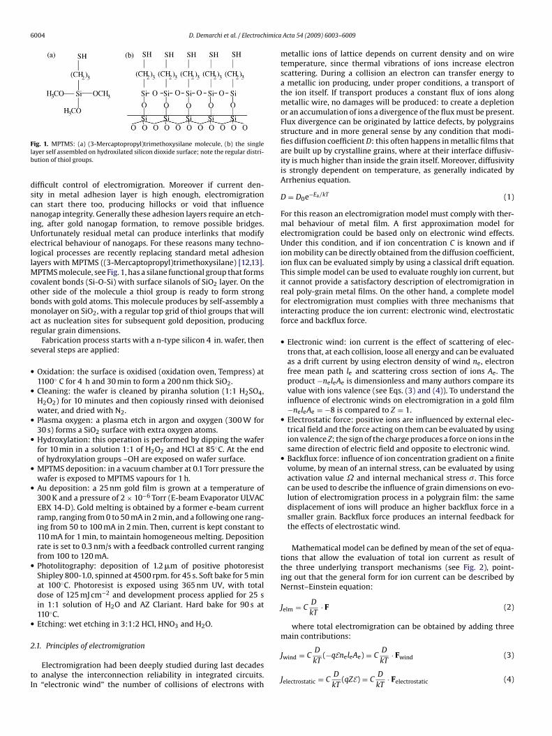
6004 D. Demarchi et al. / Electrochimica
Flb
dscniUellMcobmar
s
•
•
•
•
•
•
•
•
2
tI
ig. 1. MPTMS: (a) (3-Mercaptopropyl)trimethoxysilane molecule, (b) the singleayer self assembled on hydroxilated silicon dioxide surface; note the regular distri-ution of thiol groups.
ifficult control of electromigration. Moreover if current den-ity in metal adhesion layer is high enough, electromigrationan start there too, producing hillocks or void that influenceanogap integrity. Generally these adhesion layers require an etch-
ng, after gold nanogap formation, to remove possible bridges.nfortunately residual metal can produce interlinks that modifylectrical behaviour of nanogaps. For these reasons many techno-ogical processes are recently replacing standard metal adhesionayers with MPTMS ((3-Mercaptopropyl)trimethoxysilane) [12,13].
PTMS molecule, see Fig. 1, has a silane functional group that formsovalent bonds (Si-O-Si) with surface silanols of SiO2 layer. On thether side of the molecule a thiol group is ready to form strongonds with gold atoms. This molecule produces by self-assembly aonolayer on SiO2, with a regular top grid of thiol groups that will
ct as nucleation sites for subsequent gold deposition, producingegular grain dimensions.
Fabrication process starts with a n-type silicon 4 in. wafer, theneveral steps are applied:
Oxidation: the surface is oxidised (oxidation oven, Tempress) at1100◦ C for 4 h and 30 min to form a 200 nm thick SiO2.Cleaning: the wafer is cleaned by piranha solution (1:1 H2SO4,H2O2) for 10 minutes and then copiously rinsed with deionisedwater, and dried with N2.Plasma oxygen: a plasma etch in argon and oxygen (300 W for30 s) forms a SiO2 surface with extra oxygen atoms.Hydroxylation: this operation is performed by dipping the waferfor 10 min in a solution 1:1 of H2O2 and HCl at 85◦C. At the endof hydroxylation groups –OH are exposed on wafer surface.MPTMS deposition: in a vacuum chamber at 0.1 Torr pressure thewafer is exposed to MPTMS vapours for 1 h.Au deposition: a 25 nm gold film is grown at a temperature of300 K and a pressure of 2 × 10⁻⁶ Torr (E-beam Evaporator ULVACEBX 14-D). Gold melting is obtained by a former e-beam currentramp, ranging from 0 to 50 mA in 2 min, and a following one rang-ing from 50 to 100 mA in 2 min. Then, current is kept constant to110 mA for 1 min, to maintain homogeneous melting. Depositionrate is set to 0.3 nm/s with a feedback controlled current rangingfrom 100 to 120 mA.Photolitography: deposition of 1.2 �m of positive photoresistShipley 800-1.0, spinned at 4500 rpm. for 45 s. Soft bake for 5 minat 100◦C. Photoresist is exposed using 365 nm UV, with totaldose of 125 mJ cm−2 and development process applied for 25 sin 1:1 solution of H2O and AZ Clariant. Hard bake for 90 s at110◦C.Etching: wet etching in 3:1:2 HCl, HNO3 and H2O.
.1. Principles of electromigration
Electromigration had been deeply studied during last decadeso analyse the interconnection reliability in integrated circuits.n “electronic wind” the number of collisions of electrons with
Acta 54 (2009) 6003–6009
metallic ions of lattice depends on current density and on wiretemperature, since thermal vibrations of ions increase electronscattering. During a collision an electron can transfer energy toa metallic ion producing, under proper conditions, a transport ofthe ion itself. If transport produces a constant flux of ions alongmetallic wire, no damages will be produced: to create a depletionor an accumulation of ions a divergence of the flux must be present.Flux divergence can be originated by lattice defects, by polygrainsstructure and in more general sense by any condition that modi-fies diffusion coefficient D: this often happens in metallic films thatare built up by crystalline grains, where at their interface diffusiv-ity is much higher than inside the grain itself. Moreover, diffusivityis strongly dependent on temperature, as generally indicated byArrhenius equation.
D = D0e−Ea/kT (1)
For this reason an electromigration model must comply with ther-mal behaviour of metal film. A first approximation model forelectromigration could be based only on electronic wind effects.Under this condition, and if ion concentration C is known and ifion mobility can be directly obtained from the diffusion coefficient,ion flux can be evaluated simply by using a classical drift equation.This simple model can be used to evaluate roughly ion current, butit cannot provide a satisfactory description of electromigration inreal poly-grain metal films. On the other hand, a complete modelfor electromigration must complies with three mechanisms thatinteracting produce the ion current: electronic wind, electrostaticforce and backflux force.
• Electronic wind: ion current is the effect of scattering of elec-trons that, at each collision, loose all energy and can be evaluatedas a drift current by using electron density of wind ne, electronfree mean path le and scattering cross section of ions Ae. Theproduct −neleAe is dimensionless and many authors compare itsvalue with ions valence (see Eqs. (3) and (4)). To understand theinfluence of electronic winds on electromigration in a gold film−neleAe = −8 is compared to Z = 1.
• Electrostatic force: positive ions are influenced by external elec-trical field and the force acting on them can be evaluated by usingion valence Z; the sign of the charge produces a force on ions in thesame direction of electric field and opposite to electronic wind.
• Backflux force: influence of ion concentration gradient on a finitevolume, by mean of an internal stress, can be evaluated by usingactivation value ˝ and internal mechanical stress �. This forcecan be used to describe the influence of grain dimensions on evo-lution of electromigration process in a polygrain film: the samedisplacement of ions will produce an higher backflux force in asmaller grain. Backflux force produces an internal feedback forthe effects of electrostatic wind.
Mathematical model can be defined by mean of the set of equa-tions that allow the evaluation of total ion current as result ofthe three underlying transport mechanisms (see Fig. 2), point-ing out that the general form for ion current can be described byNernst–Einstein equation:
Jelm = CD
kT· F (2)
where total electromigration can be obtained by adding threemain contributions:
Jwind = CD
kT(−qEneleAe) = C
D
kT· Fwind (3)
Jelectrostatic = CD
kT(qZE) = C
D
kT· Felectrostatic (4)
D. Demarchi et al. / Electrochimica Acta 54 (2009) 6003–6009 6005
Fd
J
mzf
staerfi
2
oaagmsdmehnitciglf
ts
itbi
a lower voltage since the current is focused in the section weakenedby gaps and depleted grains. The abrupt temperature increase pro-duces a stronger electromigration with larger gap formation, againthe voltage bias must be removed to reduce the risks of modifyingagain the grain where the nanogap was produced. If this procedure
ig. 2. Forces acting on the metal ion dipped in the electron flow: the electronensity ne is considered constant and the ions density C decreases from left to right
backflux = −D∂C
∂x= −DC�
∂�
∂x= C
D
kT(−qVT �
∂�
∂x) = C
D
kT· Fbackflux
(5)
Ion current can produce regions of depletion (void) and of accu-ulation (hillhock), only if the divergence of ion flux becomes non
ero. A monodimensional continuity equation can be expressed asunction of total ion current:
∂C
∂t= −∂Jelm
∂x(6)
Recently some authors by using a mean value for grain dimen-ions and for the diffusivity rewrote the continuity equation inerms of ion vacancies instead of metal ions, and they found somenalytical solutions showing as the current coefficient in the Black’squations can be derived from the model. Unfortunately theseesults cannot be used to study the specific behaviour of the metallm during break formation.
.2. Grain dimensions influence on nanogaps formation
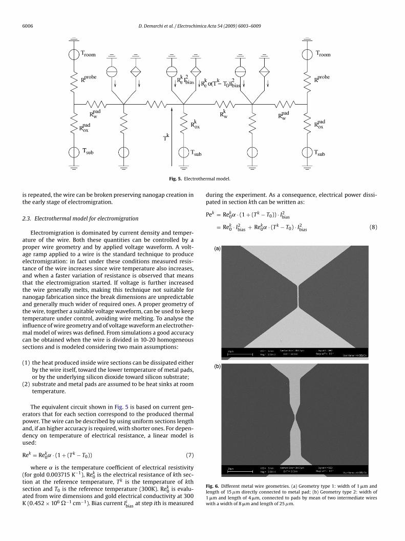
In a deposited metal film grain dimensions depend on densityf surface nucleation sites, on temperature and on used materi-ls. Grain dimensions can vary from few nanometers to microns. Ingold thin film evaporated at low temperature grain structure is
enerally columnar and in our realisation the line width of 1 �m isuch larger than average grain size, as shown in FESEM (Field Emis-
ion Scanning Electron Microscopy) image in Fig. 3. The geometry ofesigned wires and current density in polygrain structure originateainly a grain boundary diffusion ion current. Since we are inter-
sted to control nanogap dimension, it is important to understandow the different electromigration mechanisms interact duringanogap formation. In first phase, grain boundary diffusion dom-
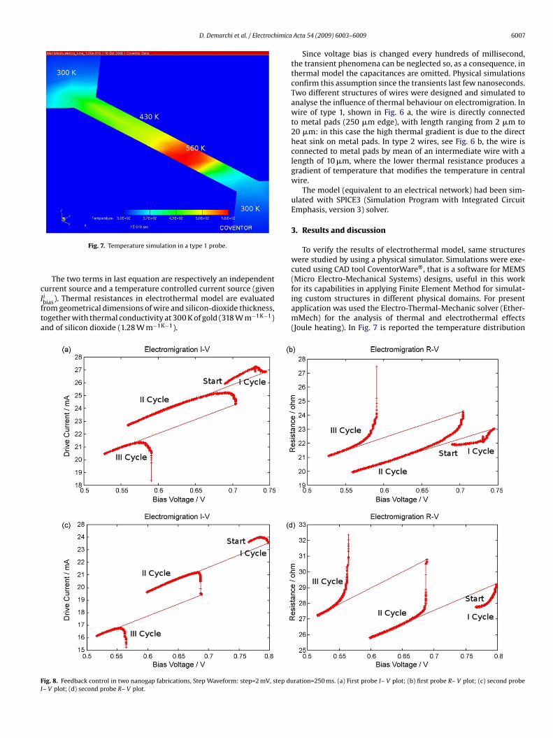
nates electromigration process: total ion current is distributed onhe boundary of all possible grains and the presence of triple pointan produce depletion and accumulation regions. In fact, as shownn Fig. 4, the sum of ion fluxes in a triple point can be less orreater than zero, by producing respectively depleted or accumu-ated regions. If grain size is smaller, there are more opportunitiesor multiple triple points.
In this regime backflux effect is limited on single grain, wherehe effect of metal atoms displacement is an increasing internaltress that limits a further movement of atoms inside the grain.
Since backflux force is higher in smaller grains, the equilibriums reached before in small grains and a net ion flux will continue onhe boundary of larger grain, where a greater amount of ions muste transported to create a balanced backflux current. If bias voltage
s constant an equilibrium condition is reached without a substan-
Fig. 3. Grains dimension in the gold film.
tial increasing of wire resistance: apparently, in the wire cannot beobserved any void or hillock but larger grains are weakened due todepletion regions. When bias voltage is further increased, it is quiteclear that this internal feedback mechanism can produce a newequilibrium condition with additional ions transport. This meansthat this regime can create voids at the border of larger grains,ensuring a smooth process most favourable to nanogaps formationduring early stage of break creation. The such formed gaps increasewire resistance and consequently current density and temperatureof the middle region of the wire, so it is fundamental to remove, assoon as possible, the voltage bias, to avoid an uncontrolled electro-migration or melting.
After few seconds the wire is again at room temperature and, ifit is applied a lower voltage bias, the current density in the wire sec-tion with higher resistance is approximately at the initial level andtherefore too low to produce electromigration. Then bias voltage isincreased as during previous cycle and electromigration will start at
Fig. 4. Depletion and accumulation produced by triple points on a grain.
6006 D. Demarchi et al. / Electrochimica Acta 54 (2009) 6003–6009
rother
it
2
apaetattnattimcs
(
(
epadu
R
(tsaK
pated in section kth can be written as:
Pek = Rek0˛ · (1 + (Tk − T0)) · I2
bias
= Rek0 · I2
bias + Rek0˛ · (Tk − T0) · I2
bias (8)
Fig. 5. Elect
s repeated, the wire can be broken preserving nanogap creation inhe early stage of electromigration.
.3. Electrothermal model for electromigration
Electromigration is dominated by current density and temper-ture of the wire. Both these quantities can be controlled by aroper wire geometry and by applied voltage waveform. A volt-ge ramp applied to a wire is the standard technique to producelectromigration: in fact under these conditions measured resis-ance of the wire increases since wire temperature also increases,nd when a faster variation of resistance is observed that meanshat the electromigration started. If voltage is further increasedhe wire generally melts, making this technique not suitable foranogap fabrication since the break dimensions are unpredictablend generally much wider of required ones. A proper geometry ofhe wire, together a suitable voltage waveform, can be used to keepemperature under control, avoiding wire melting. To analyse thenfluence of wire geometry and of voltage waveform an electrother-
al model of wires was defined. From simulations a good accuracyan be obtained when the wire is divided in 10-20 homogeneousections and is modeled considering two main assumptions:
1) the heat produced inside wire sections can be dissipated eitherby the wire itself, toward the lower temperature of metal pads,or by the underlying silicon dioxide toward silicon substrate;
2) substrate and metal pads are assumed to be heat sinks at roomtemperature.
The equivalent circuit shown in Fig. 5 is based on current gen-rators that for each section correspond to the produced thermalower. The wire can be described by using uniform sections lengthnd, if an higher accuracy is required, with shorter ones. For depen-ency on temperature of electrical resistance, a linear model issed:
ek = Rek0˛ · (1 + (Tk − T0)) (7)
where ˛ is the temperature coefficient of electrical resistivity
for gold 0.003715 K−1), Rek0 is the electrical resistance of kth sec-ion at the reference temperature, Tk is the temperature of kthection and T0 is the reference temperature (300K). Rek
0 is evalu-ted from wire dimensions and gold electrical conductivity at 300(0.452 × 10⁶ �−1 cm−1). Bias current Ii
bias at step ith is measured
mal model.
during the experiment. As a consequence, electrical power dissi-
Fig. 6. Different metal wire geometries. (a) Geometry type 1: width of 1 �m andlength of 15 �m directly connected to metal pad; (b) Geometry type 2: width of1 �m and length of 4 �m, connected to pads by mean of two intermediate wireswith a width of 8 �m and length of 25 �m.
D. Demarchi et al. / Electrochimica
cIfta
FI
Fig. 7. Temperature simulation in a type 1 probe.
The two terms in last equation are respectively an independent
urrent source and a temperature controlled current source (givenibias). Thermal resistances in electrothermal model are evaluatedrom geometrical dimensions of wire and silicon-dioxide thickness,ogether with thermal conductivity at 300 K of gold (318 W m−1K−1)nd of silicon dioxide (1.28 W m−1K−1).ig. 8. Feedback control in two nanogap fabrications, Step Waveform: step=2 mV, step du– V plot; (d) second probe R– V plot.
Acta 54 (2009) 6003–6009 6007
Since voltage bias is changed every hundreds of millisecond,the transient phenomena can be neglected so, as a consequence, inthermal model the capacitances are omitted. Physical simulationsconfirm this assumption since the transients last few nanoseconds.Two different structures of wires were designed and simulated toanalyse the influence of thermal behaviour on electromigration. Inwire of type 1, shown in Fig. 6 a, the wire is directly connectedto metal pads (250 �m edge), with length ranging from 2 �m to20 �m: in this case the high thermal gradient is due to the directheat sink on metal pads. In type 2 wires, see Fig. 6 b, the wire isconnected to metal pads by mean of an intermediate wire with alength of 10 �m, where the lower thermal resistance produces agradient of temperature that modifies the temperature in centralwire.
The model (equivalent to an electrical network) had been sim-ulated with SPICE3 (Simulation Program with Integrated CircuitEmphasis, version 3) solver.
3. Results and discussion
To verify the results of electrothermal model, same structureswere studied by using a physical simulator. Simulations were exe-cuted using CAD tool CoventorWare®, that is a software for MEMS(Micro Electro-Mechanical Systems) designs, useful in this work
for its capabilities in applying Finite Element Method for simulat-ing custom structures in different physical domains. For presentapplication was used the Electro-Thermal-Mechanic solver (Ether-mMech) for the analysis of thermal and electrothermal effects(Joule heating). In Fig. 7 is reported the temperature distributionration=250 ms. (a) First probe I– V plot; (b) first probe R– V plot; (c) second probe
6 imica Acta 54 (2009) 6003–6009
fdsawa
pff
pcsworttsrd
radpoftdn
maawmov
wfiatitdrttetvbp
sadtthow
008 D. Demarchi et al. / Electroch
or a type 1 structure, similar to the one showed in Fig. 6. Theimensions of the probe are the same as the ones used in realisedtructures, with a 1�m width for the thinner wire in the centre,length of 15 �m and a gold thickness of 25 nm. These resultsere used to validate the electrothermal model and showed a good
ccordance to the values obtained from SPICE simulations.As can be clearly seen in Fig. 7, injected current produces a tem-
erature that is higher in thinner section of the probe, proving theact that where the nanogap is created the effect of temperature isundamental.
The setup at �Lab laboratory is based on the use of two micro-robes that are placed on metal pads for obtaining the electricalontact with the probe. It was then implemented a data acquisitionystem that includes a front-end circuit, realised to drive the microire with a controlled bias voltage supplying a maximum current
f hundreds of mA. The front-end must also be able to measure theeal time current flowing in the wire to evaluate resistance varia-ion: it is able to measure currents ranging from hundreds of mAo some nA with a good resolution. In such a way, when nanogapeparation does not overcome few nanometers, the tunnelling cur-ent can be measured, even if this measure was experimentallyifficult.
In EIBJ technique we applied a software controlled voltage step-amp to the wire, monitoring the real-time resistance to implementn effective feedback algorithm according to the phenomenaescribed in Section 2.2. Control algorithm uses the informationrovided by the electrothermal model to control the temperaturef the micro wire and to keep the conditions favourable to nanogapormation. A first relevant result is related to control algorithm: ifhe feedback in the control is not used, generally thermal runawayestroys the wire and any calibration of the input waveform doesot improve results.
Nanogap fabrication begins with a low voltage DC measure-ent, used to estimate the total resistance of the wire. Since probe
nd access pad resistances are well known, an initial bias volt-ge is evaluated to force a defined initial current density in theire: in our case the standard cross section of wires is approxi-ately 0.025 �m2and a current of 25 mA produces a current density
f 108 A cm−2. This current density can be considered a thresholdalue for electromigration process.
If a constant bias voltage is applied, self heating of the wireill increase the resistance, reducing the current: on the other side
rom the simulated electrothermal model a steady state conditions reached in few microseconds, with a constant temperature andconstant measured bias current. At each step of the input voltage
he temperature, and consequently the resistance of the wire, willncrease, even if electromigration does still not modify wire sec-ion. Implemented algorithm must distinguish resistance variationue to the temperature increasing from a higher variation rate of theesistance that is related to electromigration process. For this reasonhe algorithm will continue to increase bias voltage until the resis-ance has an increase of more than a predefined percentage (5% forach measured value) with respect to the last measured result. Athat time, to avoid a thermal runaway, the algorithm removes biasoltage for ten seconds and restarts the procedure from a reducedias voltage, to keep the estimated maximum current density to theredefined value.
The effects of this algorithm are evident in Fig. 8 where arehown the current vs. bias voltage and the resistance vs. bias volt-ge respectively, for two different experiments. In each plot theifferent branches are labelled with the cycle number, to show
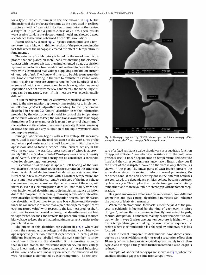
he different phases of the algorithm. It is interesting to noticehat in each branch the resistance dependency on bias voltageas a linear region as direct consequence of thermal behaviourf the wire and a non linear region where the variation of theire resistance is dominated by electromigration. The tempera-Fig. 9. Nanogaps captured by FESEM Microscope, (a) 8.1 nm nanogap, 600k×magnification; (b) 5.5 nm nanogap, 500k ×magnification.
ture of a fixed resistance value should vary as a quadratic functionof applied voltage. Since electrical resistance of the gold wirepresents itself a linear dependence on temperature, temperatureitself and the corresponding resistance have a linear behaviour ifthe effect of the dissipated power on the wire is only thermal, asshown in the plots. The linear parts of each branch present thesame slope, since it is related to electrothermal parameters. Onthe other hand, if the non linear regions in the different branchesare compared, the dependency on bias voltage becomes strongercycle after cycle. This implies that the electromigration is initially“smoother” and more favourable to create gap with nanometer sep-aration.
Designed microwires were used to understand how differentgeometries and bias control algorithm parameters can influencethe quality of fabricated nanogaps.
When the electrothermal feedback is used the yield of the pro-cess is evidently influenced by the kind of geometry. In wiresof type 1, where the micro-wire is directly connected to pads,thermal dissipation is enhanced making easier temperature con-trol, while in type 2 wires average temperature is higher, with alower temperature gradient along the wire: as a consequence theregion where electromigration is enhanced by temperature is lessfocused.
These different temperature distributions have direct conse-quence on process yield: considering good a separation of less than
10 nm, type 1 wires have an higher yield (approximately twice) thantype 2, and for type 1 the yield is further increased if wire length isreduced.Examples of fabricated nanogaps are shown in Fig. 9, where thesmallest obtained gap is 5.5 nm, from a type 1 wire.
imica
4
cAadofiaovbtiTdida
[
[11] Z.M. Wu, M. Steinacher, R. Huber, M. Calame, S. van der Molen, C. Schnenbergera,
D. Demarchi et al. / Electroch
. Conclusions
A room temperature technological process for nanogap fabri-ation based on EIBJ technique had been realised and optimised.
reliable process for gold thin film, based on a monolayer selfssembly adhesion layer, was used by authors as starting point toefine an electrothermal model able to control the temperaturef the microwire during electromigration. This model was veri-ed for different geometries and used to control voltage waveformspplied to gold microwire. The influence of gold grain nucleationn the nanogap development was studied and experimentallyerified. These information was collected and used to tune a feed-ack algorithm. Obtained results show a good accordance betweenhe foreseen effects of temperature on internal mechanisms act-ng during nanogap formation and the final nanogap dimensions.
he smallest produced nanogap has a width of 5.5 nm. A furtherevelopment of the mathematical model for electromigration, tak-ng into account internal temperature distribution, will be furthereveloped for improving the yield of the process and for obtaininggood control in nanogap dimensions and characteristics.
[
[
Acta 54 (2009) 6003–6009 6009
References
[1] J.M. Tour, Account Of Chemical Research 33 (11) (2000) 791.[2] M.D. Ventra, S.T. Pantelides, N.D. Lang, Applied Physics Letters 76 (23) (2000)
3448.[3] H. Shiigi, S. Tokonami, H. Yakabe, T. Nagaoka, Journal of American Chemical
Society (JACS) 127 (2005) 3280.[4] S.M. Dirk, S.W. Howell, S. Zmuda, K. Childs, M. Blain, R.J. Simonson, D.R. Wheeler,
Nanotechnology 16 (2005) 1983.[5] M. Yi, K.-H. Jeong, L.P. Lee, Biosensors and Bioelectronics 20 (2005) 1320.[6] J. Baker-Jarvis, C. Jones, B. Riddle, Technical report, 1998.[7] S. Oh, J.S. Lee, K.-H. Jeong, L.P. Lee, Micro Electro Mechanical Systems MEMS-03,
2003, p. 52.[8] A.F. Morpurgo, C.M. Marcusa, D.B. Robinson, Applied Physics Letters 74 (14)
(1999) 2084.[9] H. Park, A.K.L. Lim, A.P. Alivisatos, Applied Physics Letters 75 (2) (1999)
301.10] V.C.-Y. Shih, S. Zheng, A. Chang, Y.-C. Tai, 12th International Conference on Solid
State Sensors Actuators and Microsystems, 2003.
Applied Physics Letter 91 (2007) 053118.12] A.K. Mahapatro, S. Ghosh, D.B. Janes, IEEE Transactions on Nanotechnology 5
(3) (2006) 232.13] A.K. Mahapatro, A. Scott, A. Manning, D.B. Janesa, Applied Physics Letters 88
(2006) 151917.