stratified fiber-resonator: fabrication, characterization and
160
STRATIFIED FIBER-RESONATOR: FABRICATION, CHARACTERIZATION AND POTENTIAL APPLICATIONS by Zeba Naqvi A dissertation submitted to the faculty of The University of North Carolina at Charlotte in partial fulfillment of the requirements for the degree of Doctor of Philosophy in Optical Science and Engineering Charlotte 2017 Approved by: ______________________________ Dr. Tsing-Hua Her ______________________________ Dr. Faramarz Farahi ______________________________ Dr. Greg J. Gbur ______________________________ Dr. Shunji Egusa _____________________________ Dr. Stuart T. Smith
-
Upload
khangminh22 -
Category
Documents
-
view
0 -
download
0
Transcript of stratified fiber-resonator: fabrication, characterization and

STRATIFIED FIBER-RESONATOR: FABRICATION, CHARACTERIZATION AND
POTENTIAL APPLICATIONS
by
Zeba Naqvi
A dissertation submitted to the faculty of
The University of North Carolina at Charlotte
in partial fulfillment of the requirements
for the degree of Doctor of Philosophy in
Optical Science and Engineering
Charlotte
2017
Approved by:
______________________________
Dr. Tsing-Hua Her
______________________________
Dr. Faramarz Farahi
______________________________
Dr. Greg J. Gbur
______________________________
Dr. Shunji Egusa
_____________________________
Dr. Stuart T. Smith

ii
©2017
Zeba Naqvi
ALL RIGHTS RESERVED

iii
ABSTRACT
ZEBA NAQVI. Stratified Fiber-Resonator: Fabrication, Characterization and Potential
Applications. (Under the direction of DR. TSING-HUA HER)
Whispering Gallery Mode Resonators (WGMR) are compact, monolithic
resonators used for photonic applications. Controlling the properties of WGM while
keeping the geometry simple is desired to improve their performance, especially for
sensing and non-linear interactions. One way to achieve this is by coating the WGMR with
a layer of certain refractive index profile, which has been shown to modify the effective
optical potential thus allowing control of the WGM field. This dissertation focusses on
coating of an optical fiber with single or multiple thin films with precise control of
thickness and refractive index. Transfer matrix method is applied to study the effect of
coated films on the mode structures and field profiles of fiber WGM. For small layer
thickness the mode shifts to the periphery while for large thicknesses waveguide modes
are found and coupling is observed for multiple layers. Fibers are coated uniformly in a
commercial PECVD instrument modified to enable continuous rotation of fibers. Mie
scattering of coated fibers is utilized to extract refractive index and thickness of coated thin
films, which is otherwise challenging due to non-flat topology and small size of the fibers.
It is found that rotation leads to higher deposition rate and refractive index of films,
compared to those deposited on a static wafer. These differences are demonstrated to
depend on the rotation speed, opening interesting dynamic tuning capabilities. Further,
fibers with Bragg layers are fabricated and their scattering analyzed. It is found that
judicious choice of film thickness can drastically modify scattering signatures of Bragg

iv
fibers. A ray model taking into account photonic bandgap of Bragg layers is proposed to
successfully explain these anomalous features.

v
DEDICATION
To my parents

vi
ACKNOWLEDGEMENTS
My long pending gratitude to my PhD supervisor Dr. Tsing-Hua Her. Five years
with him transformed me positively at several levels. The freedom he gave me to argue
with him based on evidence awakened some dormant energies in me. I might miss that
environment where logic reigns supreme. I will also miss the Chinese peanuts he offered
to calm me down in our heated discussions. He valued me for who I am and accepted my
idiosyncrasies as much as I did his. Thanks for teaching me several soft and hard skills
patiently despite occasional locking of horns of true Taurean bulls that we both are.
Complementary to the energetic and ecstatic personality of Dr. Her, were the gentle
souls like Dr. Farahi, Dr. Fiddy and Dr. Smith. Witnessing Dr. Fiddy’s unmatched people
skills, generosity and ultra-efficient management first hand was an enriching experience in
itself apart from his insights in the field of scattering. Dr. Farahi’s support in my rough
times saved me a lot of trouble. His faith in my abilities toned down my imposter syndrome.
Speaking of support, Dr. Angela Davies deserves the credit for my finishing PhD in time.
Hats off to her for giving me her precious time amidst a heap of responsibilities only she
can handle. Big thanks to Dr. Smith who always had our back for electronics and
mechanical engineering problems. Thanks to Dr. Egusa for sharing his most up-to-date
knowledge on all sorts of multilayered fibers. I would also like to thank Dr. Gbur for his
openness to discuss ideas on scattering even outside this project.
One great acquaintance I fortunately made was Dr. Lisa Russell Pinson who taught
me that PhD is just the beginning. This realization reset my mind which was lost in striving
for unattainable perfection. She supported me behind the scenes for nearly two years
selflessly. While on the foreground were my lab mates - Mark Green and Yuanye Liu,

vii
always there for technical and non-technical discussions sweeping a breadth of physical
and metaphysical topics. Joseph Peller deserves a special mention for being a true friend-
in-need throughout my 5 years at UNC Charlotte. Frances, Jonathan, Ali, Nasim, Farzaneh,
Elisa, Patrick, Hossein and many more made my stay here memorable. Thanks to Dr.
Asmaa Getan of Math department for her love and free food.
People from my past, Dr. Vasant Natarajan from Indian Institute of Science and Dr.
Hema Ramachandran from Raman Research Institute, Bangalore deserve a special mention.
These were the scientists who took a chance and let an IT major do experimental atomic
physics in their labs. On the other hand discussions with Dr. R. Srikanth on theoretical
concepts happened at a higher level of existence, devoid of ego and driven by pure spirit
of enquiry. He reassured my faith in physics as a means to reach the truth. Of course he
struggles for funding in a world that has forgotten the importance of curiosity that leads to
great theories and serendipities. I also thank my friends RK, UT and ET for being
supportive from my high school days.
Special thanks to my nephews and nieces Haider, Zahra, Zainab, Naaz and little
Naqi spread across the globe. Their innocence and sweet voices are like a healing potion
to a stressed mind. Thanks to my brothers-in-law and sisters for encouraging me to take
risks I am fond of. Lastly, gratitude to my parents is best unsaid. Expressing it in words
will belittle their magnanimous position in my life. This dissertation and every good thing
I will ever do is dedicated to them.

viii
TABLE OF CONTENTS
LIST OF TABLES ............................................................................................................. xi
LIST OF FIGURES .......................................................................................................... xii
LIST OF SYMBOLS/ABBREVIATIONS .................................................................... xviii
INTRODUCTION ........................................................................................ 1
1.1 Motivation ............................................................................................................ 1
1.2 Outline .................................................................................................................. 7
WHISPERING-GALLERY MODE RESONANCE IN COATED FIBERS 8
2.1 Introduction .......................................................................................................... 8
2.2 Transfer Matrix Method for Multilayered Fibers ................................................. 8
2.3 Results ................................................................................................................ 11
2.3.1 Uncoated vs Coated Fiber WGMR ............................................................. 11
2.3.2 Fundamental Mode as a Function of Layer Thickness ............................... 12
2.3.3 Higher Order Mode Profiles ....................................................................... 14
2.3.4 Effect of Layer Thickness on Fundamental Mode Resonant Wavelength . 15
2.3.5 WGM in Three Layer Structure .................................................................. 17
FABRICATION OF COATED FIBERS.................................................... 19
3.1 Introduction ........................................................................................................ 19
3.1.1 Overview of Vapor Deposition Methods Used for Multilayered Fibers .... 19
3.1.2 PECVD for wafers: General Principle and Chemical reactions ................. 21
3.2 Experiment ......................................................................................................... 23
3.2.1 PECVD Adapted for Coating Optical Fibers .............................................. 23
3.2.2 Fabrication Procedure ................................................................................. 25
3.3 Results ................................................................................................................ 26
3.3.1 Single-Layered Optical Fibers .................................................................... 26
3.3.2 Multilayered Optical Fibers ........................................................................ 30
3.3.3 Uniformity of Layers .................................................................................. 33
3.3.4 Coated NIST’s Microrod Resonator ........................................................... 35
CHARACTERIZATION OF THIN FILMS ON OPTICAL FIBERS ....... 39
4.1 Introduction ........................................................................................................ 39
4.2 Theory of Scattering from Layered Fibers ......................................................... 40

ix
4.3 Experiment ......................................................................................................... 45
4.4 Scattering Data for Single Layered Fiber ........................................................... 48
4.5 Data Analysis ..................................................................................................... 54
4.5.1 Algorithm for Characterization of Fibers ................................................... 54
4.5.2 Results ......................................................................................................... 56
4.5.3 Challenges using Backscattering ................................................................ 69
4.5.4 Alternatives ................................................................................................. 71
MIE SCATTERING OF BRAGG FIBERS ............................................... 80
5.1 Introduction ........................................................................................................ 80
5.2 Experimental Data .............................................................................................. 80
5.3 Theory and Comparison to Experimental Data .................................................. 83
5.4 Scattering Angle Diagram .................................................................................. 85
5.4.1 Augmented Scattering Angle Diagram for Bare Fiber ............................... 88
5.4.2 Augmented Scattering Angle Diagram for Bragg Fiber ............................. 89
CONCLUSION AND FUTURE WORK ................................................... 94
REFERENCES ................................................................................................................. 98
APPENDIX A Matlab Code for WGM in Bragg Fibers ............................................ 103
A.1 Program Structure ................................................................................................ 103
A.2 Instructions to Run the GUI ................................................................................. 104
A.3 Dispersion Map Calculation ................................................................................. 105
A.3.1 BraggResonator.m ......................................................................................... 105
A.3.2 disperion_1point.m ....................................................................................... 108
A.3.3 dispersion_1point_ ........................................................................................ 109
A.3.4 BraggResonator_NRM.m ............................................................................. 111
A.4 Algorithm for Quick Root Search ........................................................................ 112
A.4.1 Newton Raphson Method in 2D.................................................................... 112
A.5 The GUI Code Explained ..................................................................................... 114
APPENDIX B PECVD Operation for Fiber Coating ................................................ 123
B.1 Operating Instructions for Fabrication of Coated Fiber ....................................... 123
B.2 Software Interface ................................................................................................ 126
B.2.1 Recipes for Silicon Nitride and Silica ........................................................... 127
APPENDIX C SEM of Films Deposited by PECVD ................................................ 130

x
C.1 Calibration of Deposition Rate by SEM .............................................................. 130
C.1.1 Single Fiber with Multiple Layers ................................................................ 130
C.1.2 Multiple Fibers with Single Layer Deposition .............................................. 138
APPENDIX D SPEED DEPENDENT REFRACTIVE INDEX ............................... 139
D.1 Experiment and Results ....................................................................................... 139
D.2 Discussion ............................................................................................................ 141

xi
LIST OF TABLES
Table 1: Calibration of Bare FT200EMT using backscattering. ....................................... 57
Table 2: Calibration of Bare SMF28 using backscattering ............................................... 58
Table 3: Result for SiNx Root Search using backscattering .............................................. 60
Table 4: Result for SiO2 Root Search using backscattering. ............................................. 61
Table 5: Root search result for error bar calculation on ZN9 ........................................... 66
Table 6: Scattering vs SEM results for SiNx ..................................................................... 68
Table 7: Thickness characterization by scattering for SiO2 .............................................. 68
Table 8: Root (2r1, n2, t) for 3D search using scattering data 10⁰ – 175⁰. ........................ 77
Table 9: Root (2r1, n2, t) for 3D search using scattering data 10⁰ – 175⁰. ........................ 79
Table 10: Layer sequence for multilayered fiber for growth rate calibration. ................ 131
Table 11: Thicknesses obtained from SEM images of layers for the 3 points around the
cross section. ................................................................................................................... 137
Table 12: Thickness obtained from SEM of 4 single layered fibers. .............................. 138
Table 13: Roots search result .......................................................................................... 140

xii
LIST OF FIGURES
Figure 1.1: Potential function for a 100 µm dielectric cylinder coated with high
index dielectric layer. Blue line marks the total energy. ................................. 2
Figure 1.2: Radial function of WGM field in a microsphere coated with layer of
n=1.6 and total radius 100 µm. Thickness t is indicated along each
curve. Reproduced from [5]. ............................................................................ 3
Figure 1.3: Effect of refractive index profile on the spacing of frequency comb teeth.
......................................................................................................................... 5
Figure 2.1: WGM mode in uncoated and coated fibers. The coating modifies the
radial distribution of the field. High index coating pulls the mode
toward the layer. .............................................................................................. 8
Figure 2.2: Schematic of N layered cylinder cross section showing coefficients of
outgoing (A) and incoming (B) cylindrical waves in each region of
constant refractive index. For N layers there are N+1 interfaces and
N+2 regions. .................................................................................................. 10
Figure 2.3: Normalized radial profile of WGM in uncoated (red) and coated (black)
fiber. WGM gravitates towards the coated layer (60 nm) and is also
narrower. Azimuthal order is 400. ................................................................. 12
Figure 2.4: Effect of layer thickness on radial field profile of the lowest order WGM.
nlayer = 2.4, nfiber = 1.447. Total radius is held at 62.5 µm. m = 400. ............. 13
Figure 2.5: Normalized radial E field profile of TM polarized WGM modes of
orders v=0 to 3 in an SMF fiber coated with a 100 nm layer of refractive
index 2.4. Corresponding resonant wavelengths are:
1.486,1.368,1.335,1.309res m respectively. .................................................... 14
Figure 2.6: Radial E field profile of TM polarized WGM modes of first three modes
in a fiber (n=1.447) coated with a layer of thickness 2 µm and refractive
index 2.4. The corresponding resonant wavelengths are 1.4586, 1.374,
1.342 µm respectively. m = 400. ................................................................... 15
Figure 2.7: Resonant wavelength as a function of layer thickness. Black and red
curves are for SMF coated with n=2.4 while blue and bluish green have
n=nco=1.447. Two curves for each case are for v=0 and v=1. Fiber RI
nco=1.447. The orange curve is for n=nco=2.4 which has higher resonant
wavelength, plotted on the Y axis on the right. ............................................. 16
Figure 2.8: WGM mode in 3 layer structure as a function of thickness of separation
layer T. Radial E field profile for TM polarized WGM modes in SMF
fiber (n=1.45) coated with 3 layers of high (n=1.7) low (n=1.44) high
index (n=1.7). Radius of fiber = 62.5 µm, thicknesses of high index
layers are 0.4 µm each while that of separation layer varies from 1 µm
to 10 µm. Coupling is observed between modes of the thin layers for 2
µm and beyond but the energy shifts to inner thin layer with increasing

xiii
separation. Modes correspond to lowest order i.e. longest resonant
wavelength. Azimuthal order m = 400. ......................................................... 18
Figure 3.1: Schematic of PECVD chamber ...................................................................... 22
Figure 3.2: (a) Stationary fiber has non-uniform deposition due to high flux at the
top. (b) Rotating the fiber equalizes the flux exposure creating uniform
film ................................................................................................................. 23
Figure 3.3: (a) Schematic of PECVD chamber modified for deposition on fiber. (b)
Outside view of the rotary feedthrough with a stepper motor attached
overhead. (c) Inside view of the chamber showing the circular base
platen with glass holder on the extreme end and Brass fiber chuck
diametrically opposite. Faintly visible fiber is held by the chuck and the
glass holder. View from the circular viewport on the side of holder can
be seen in (d) showing the pink plasma between the platen and
showerhead. ................................................................................................... 24
Figure 3.4: Bright field images of Thorlabs fiber FT200EMT coated with SiNx for
progressively increasing deposition times. .................................................... 28
Figure 3.5: Bright field images of Corning SMF28 coated with SiNx with increasing
deposition times. ............................................................................................ 29
Figure 3.6: Dark field image of Corning SMF28e+ coated with SiO2 for 5 mins at
30 rpm (top) and uncoated SMF28e+ (middle and bottom). ......................... 30
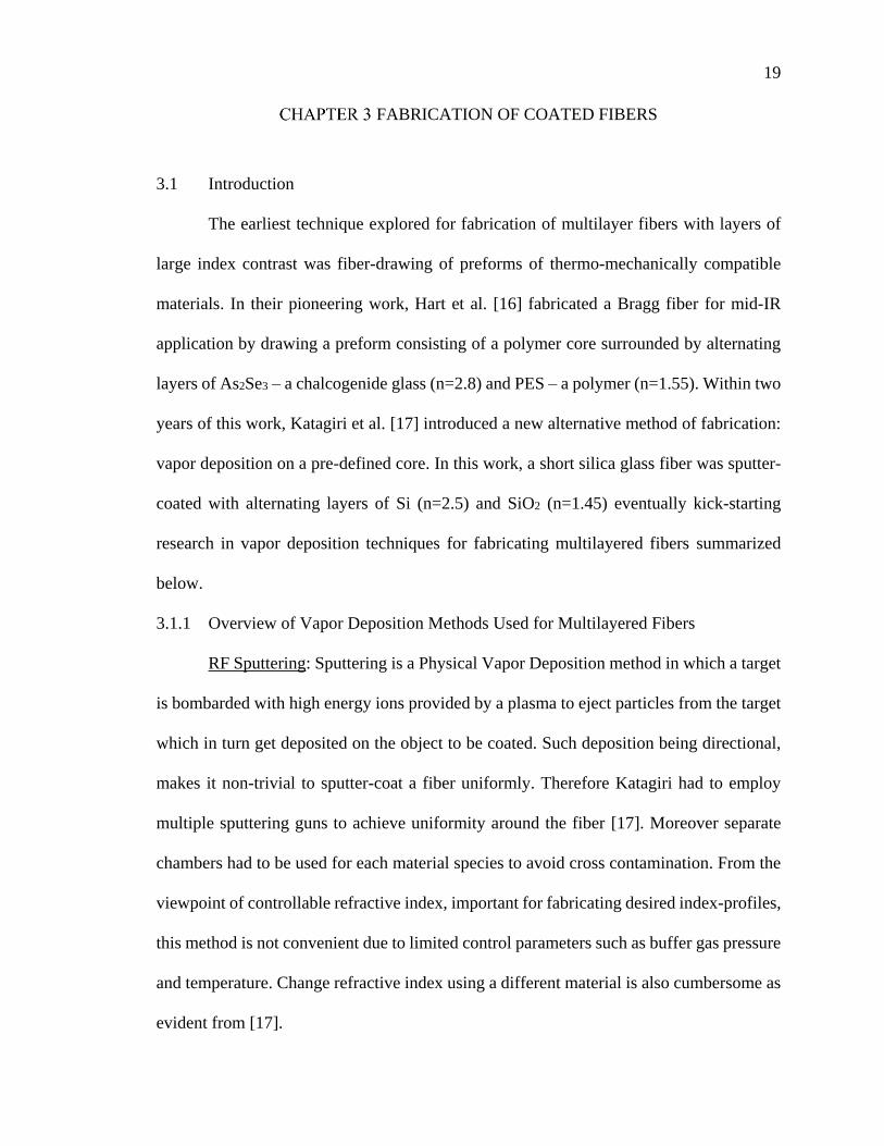
Figure 3.7: Bright field images of Bragg Fibers fabricated in PECVD. (a) ZN4 has
12 pairs of SiNx and SiO2 terminated with thick layer of SiO2 deposited
for 5 mins. (b) ZN5 also has 12 pairs of SiNx and SiO2 but with different
deposition time, and terminated in a 5 min SiO2 layer. (c) ZN27 has 4
such pairs with deposition time of 10 mins for SiNx and 36 sec for SiO2.
(Deposition Time format - mm:ss.ss) ............................................................ 31
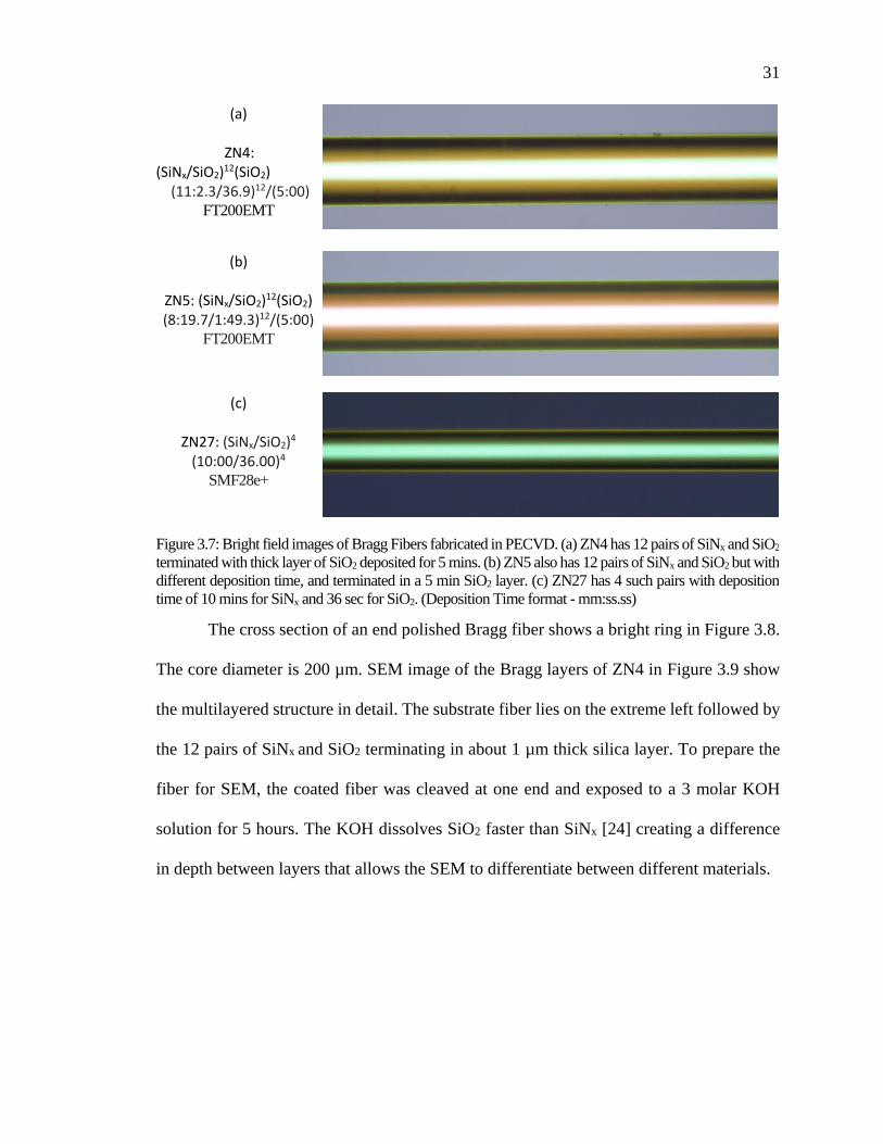
Figure 3.8: Optical microscope image of cross section of Bragg fiber with 200 µm
core. Outer bright ring consists of the Bragg layers terminated by thick
SiO2 layer. ...................................................................................................... 32
Figure 3.9: SEM image of Bragg layers of ZN4. Left to right: Substrate fiber, 12
pairs of SiNx/SiO2, terminal layer of SiO2. .................................................... 32
Figure 3.10: Non-uniform deposition near the fiber end .................................................. 33
Figure 3.11: Optical images of ZN9 taken along fiber axis. ............................................. 33
Figure 3.12: Crack in thickest layer coated (~ 3 um): ZN13. Thick layers are prone
to crack on frequent handling. ....................................................................... 34
Figure 3.13: Comparison of iridescence of Bragg fiber fabricated by rotation (ZN4)
(a) and without rotation (b). ........................................................................... 35
Figure 3.14: A comparison of thickness variation azimuthally for stationary (black
squares connected by straight line as eye guide) and rotated (blue
triangles) case. Blue dashed marks the mean value of thickness. ................. 35

xiv
Figure 3.15: The short resonator rod attached to a long 2mm diameter glass rod
with a ceramic sleeve. Metal shim was used to fill the gap between
sleeve and the 2 glass rods. ............................................................................ 36
Figure 3.16: Microrod resonators received from NIST have a milky appearance (a). When
coated without cleaning, the milky appearance turns into white debris (b)
while the resonator region remains clean. But if the resonator is cleaned (c),
the milky appearance vanishes and the coated resonator is free of any debris
(d). .................................................................................................................. 37
Figure 3.17: Resonance dip in the transmission spectrum of coated microrod
resonator has a linewidth of 90 MHz and Q-factor 2.2x10⁶ (red). The
dip for uncoated resonator (black) is shown for comparison. It has about
1 MHz linewidth. (Image credit: Pascal Del’Haye at NIST Boulder,
now at NPL - UK) .......................................................................................... 38
Figure 4.1: Schematic of experimental set-up. BS: Beam Splitter, PDA: Photodiode
Amplifier, DAQ: Data Acquisition card. Computer controls the
rotation stage and scattering signal is read through the DAQ. ...................... 46
Figure 4.2: Scatterometer for fiber characterization. ........................................................ 47
Figure 4.3: Scattering of polarized HeNe (E || fiber) from a fiber on a circular screen
with an entry hole for beam. Portion of the fiber hit by beam is marked
as fiber. Backscattering pattern can be seen with beam entry hole at the
center. ............................................................................................................. 48
Figure 4.4: Normalized backscattering patterns of FT200EMT coated with ~50 nm
layer [ZN7], taken at 90⁰ azimuthal intervals. Two patterns (red and
black) in each plot are data about symmetry axis i.e. incident beam. ........... 49
Figure 4.5: Normalized backscattering patterns of FT200EMT coated with ~100
nm layer [ZN8], taken at 90⁰ azimuthal intervals. Two patterns (red and
black) in each plot are data about symmetry axis i.e. incident beam. ........... 49
Figure 4.6: Normalized backscattering patterns of FT200EMT coated with ~250
nm layer [ZN9], taken at 90⁰ azimuthal intervals. Two patterns (red and
black) in each plot are data about symmetry axis i.e. incident beam. ........... 50
Figure 4.7: Normalized backscattering patterns of FT200EMT coated with ~500
nm layer [ZN10], taken at 90⁰ azimuthal intervals. Two patterns (red
and black) in each plot are data about symmetry axis i.e. incident beam.
....................................................................................................................... 51
Figure 4.8: Normalized backscattering patterns of SMF28 coated with silicon
nitride for 10-40 mins (Fiber ID’s are ZN19, ZN17, ZN20, ZN21
respectively). .................................................................................................. 52
Figure 4.9: LHS-RHS overlap of backscattering of ZN19 prepared using Corning
SMF28e+. ...................................................................................................... 53
Figure 4.10: Normalized backscattering patterns of SMF28 coated with silica for 3-
6 mins. (Fiber ID’s are ZN25, ZN26, ZN18, ZN24 respectively) ................. 54

xv
Figure 4.11: Difference between theoretical scattering patterns generated with the
core and without the core. .............................................................................. 58
Figure 4.12: Normalized backscattering patterns of Thorlabs FT200EMT (red) and
Corning SMF28e+ (blue). .............................................................................. 59
Figure 4.13: LSE vs Fiber Diameter for SiNx coated fibers. ............................................ 60
Figure 4.14: LSE vs Fiber Diameter for SiO2 coated fibers. ............................................. 61
Figure 4.15: Experimental data and corresponding theoretical fit for backscattering
patterns of coated fibers. Fiber ID’s top to bottom: SiNx- ZN19, ZN17,
ZN20, ZN21 with deposition times 10, 21, 30 and 40 mins respectively;
SiO2- ZN25, ZN26, ZN18, ZN24 (deposition times: 3, 4, 5, and 6 mins
respectively). .................................................................................................. 62
Figure 4.16: Refractive index and thickness as a function of deposition time
retrieved from scattering pattern of the coated fibers. Blue line is the
line of best fit while black line is located at the mean value of refractive
index. ............................................................................................................. 64
Figure 4.17: Silicon nitride growth rate curve on stationary fiber (a-b). Reproduced
from [22]. ....................................................................................................... 65
Figure 4.18: Growth rate obtained using Scattering compared to that obtained from
SEM. Left: SiNx; Right: SiO2. ....................................................................... 67
Figure 4.19: Apparent degeneracy in backscattering patterns of SMF28. (a) and (b)
are for two orthogonal orientations of the fiber. ............................................ 71
Figure 4.20: Error plot for different scattering regions. Top: 150⁰ – 180⁰, Middle:
5⁰ – 20⁰, Bottom: 0⁰ – 180⁰. .......................................................................... 72
Figure 4.21: 2D error plot for coated fiber for forward and backscattering regions. ....... 73
Figure 4.22: Full Scattering Data for coated fibers. See Figure 3.5 for complete
fiber recipes. .................................................................................................. 75
Figure 4.23: Least Square Error vs Fiber diameter plot for scattering range 10⁰ –
175⁰. ............................................................................................................... 77
Figure 4.24: 2D error plots of (t x n2) for each local minimum along the 3rd
dimension of fiber diameter. .......................................................................... 78
Figure 5.1: Polar scattering plots for Bragg Fibers. .......................................................... 82
Figure 5.2: Scattering data for TM (left) and TE (right) polarizations for bare (green)
and Bragg Fiber ZN5 (blue). ......................................................................... 84
Figure 5.3: Effect of terminal layer on scattering of TM polarized HeNe from Bragg
fiber assuming 12 pairs of SiNx and SiO2 with thicknesses 165 nm and
375 nm respectively while indexes assumed to be 2.49 and 1.6
respectively. ................................................................................................... 84
Figure 5.4: Experiment (blue) vs theoretical fit (red) for ZN5. (Left) TM; (Right)
TE. ................................................................................................................. 85

xvi
Figure 5.5: Ray diagram through fiber cross section showing only reflected and
transmitted rays. ............................................................................................. 86
Figure 5.6: Scattering angle can exceed 180⁰ for high refractive index. .......................... 87
Figure 5.7: Ray diagram and corresponding scattering angle diagram. ........................... 88
Figure 5.8: Augmented scattering angle diagrams of bare fiber for TM (left) and
TE (right) polarizations. Red curve thickness has been scaled 4 times
for visibility. .................................................................................................. 89
Figure 5.9: Scattering Angle Diagrams to explain Photonic Bandgap effect in Bragg
Fiber ZN5. (a) TM, (b) TE. ............................................................................ 91
Figure 5.10: Polar scattering patterns for several Bragg fiber designs. ............................ 92
Figure 5.11: Scattering angle diagram for ZN4. Scattering data is for TM
polarization. Parameters of Bragg layers are: nSiN=2.49, nSiO=1.6,
tSiN=236 nm, tSiO=109 nm. Again, red curve has been scaled by a
factor of 4 for visibility. ................................................................................. 93
Figure B.1: Side view of rotary feedthrough with stepper motor attached. .................... 123
Figure B.2: PECVD chamber lid opened for loading substrates directly into the
chamber instead of through loading dock. Here, the chuck with the fiber
is mounted into the rotary shaft and place the glass holder with long
groove. ......................................................................................................... 124
Figure B.3: Inside view of the chamber showing glass holder placed on the platen
and fiber chuck holding the fiber inside rotary shaft. .................................. 125
Figure B.4: Process Module interface. ............................................................................ 126
Figure B.5: Recipe selection panel. ................................................................................ 127
Figure B.6: Menu of recipes. ‘Pump to Base’ necessary before and after each
deposition of a material. .............................................................................. 128
Figure B.7: Tabs to define a recipe for material deposition. Appear on clicking
‘HFSiN’ ....................................................................................................... 128
Figure B.8: Settings for Pressure, Gase Flow rate (sccm), Generator and matching
unit for Silicon Nitride (left) and Silica (right). ........................................... 129
Figure C.1: SEM micrograph of a multilayered fiber coating. Substrate fiber
(FT200EMT), not shown in the image lies on the left side followed by
6 pairs of bilayers of SiNx and SiO2 layers making the 24 layers in the
image. The 6 deposition times for SiNx are 10, 14, 18, 22, 26 and 30
minutes, while those for SiO2 are 10, 20, 30, 40, 50 and 60 seconds.
The last layer is terminated by a thick layer of SiO2 deposited for 360
sec. ............................................................................................................... 130
Figure C.2: Zoomed-in SEM images of alternating layers of SiNx and SiO2 used to
extract thicknesses of the layers. The information bar has been cropped

xvii
out to convert the image to grayscale. Layers 1-8, 8-12, 12-16, 16-20,
20-23. ........................................................................................................... 132
Figure C.3: SEM image intensity summed top to bottom. Layers 1-6, 6-10, 10-14,
14-16, 16-20, 20-23 ..................................................................................... 133
Figure C.4: Growth Rate curve from three points around the fiber cross section. ......... 135
Figure C.5: Growth Rate curve obtained from single layers deposited on different
fibers. ........................................................................................................... 138
Figure D.1: Experimental Data vs best-fit scattering pattern for fibers fabricated at
different rotation speed. ............................................................................... 140
Figure D.2: Refractive index of SiNx films as a function of RPM determined from
scattering of the coated fibers. Four fibers were coated at 3, 15, 30 and
42 RPM respectively. ................................................................................... 141
Figure D.3: Comparison of deposition conditions for stationary, slow and fast
rotating fiber. ............................................................................................... 141

xviii
LIST OF SYMBOLS/ABBREVIATIONS
WGM
WGMR
GRIN
PECVD
SMF
RI
SEM
LSE
PBG
ZNx
Whispering Gallery Mode
WGM Resonator
Graded Index
Plasma Enhanced Chemical Vapor Deposition
Single Mode Fiber
Refractive Index
Scanning Electron Microscope
Least Square Error
Photonic Bandgap
Fiber ID#

1
INTRODUCTION
1.1 Motivation
Microresonators with whispering gallery modes (WGM) are compact, monolithic,
mirrorless resonators with high Q-factors, storing light in a small volume near the periphery
of the resonator, guided by total internal reflection. Since a WGM is concentrated near the
periphery of the resonator, coating the surface of WGM resonator (WGMR) with a radial
designer RI (refractive index) profile, graded or step index, offers a way to tune the shape
of effective optical potential [1, 2] hence control the properties of modes of the resonator
[3]. This can be understood by drawing an analogy between Schroedinger’s equation and
wave equation in optics, as in [4], where the optical potential for TM polarization in a
cylinder (E || axis) with refractive index profile n(r) as a function of radius was derived to
be:
2
2 2
2
4 11
4TM
mV k n r
r
(1.1)
Here k is the vacuum wavevector, r is the radial coordinate and m is the order of
Bessel function. The effective optical potential in a cylinder of radius 100 µm, refractive
index 1.45 shown in black in the Figure 1.1 develops a deep well when peripheral RI is
increased (n=1.7). The width, depth and shape of the potential well can be controlled by
RI profile n(r) which in turn affects the shape of the mode.

2
Figure 1.1: Potential function for a 100 µm dielectric cylinder coated with high index dielectric layer.
Blue line marks the total energy.
Even though the WGM travels near the surface of the resonator, only a small
evanescent tail protrudes outside demanding very high Q-factors. To enhance the
sensitivity of a WGM sensor, the tail needs to be either elongated for larger interaction area
with the analyte i.e. slower decay or stronger in intensity. The stronger field will induce
larger polarization in the analyte thus increasing the sensitivity. Arnold et.al [5] showed
that a microsphere coated with a high index subwavelength layer, has WGM field shifted
to the periphery and exposed more to the surroundings. Their result is reproduced in Figure
1.2. The field for uncoated case corresponds to t=0. As the thickness of the high index layer
increases (keeping the total radius of microsphere constant), the field shifts to the periphery
and is compressed exposing a stronger evanescent field. Their result triggered interest in
coated WGMRs mainly for sensing applications.
E
Uncoated

3
Figure 1.2: Radial function of WGM field in a microsphere coated with layer of n=1.6 and total radius
100 µm. Thickness t is indicated along each curve. Reproduced from [5].
A layer of graded index (GRIN) provides further freedom in tailoring the WGM
field distribution and ease of coupling more importantly. Unlike a layer of homogeneous
RI, GRIN layer can be designed to smooth out the potential barrier between external
medium and the resonator allowing efficient light coupling. Using this principle, [6]
showed that radially decreasing GRIN cladding of a Liquid Core Optical Ring Resonator
can enhance penetration depth of field coupled from outside since the mode will gravitate
toward the center where index is higher. A similar radially decreasing profile was
suggested by [7] but in solid core WGMR. In this case the field will withdraw away from
the outside into the solid core i.e. negligible evanescent tail. From sensing perspective this
is of no use. However, the mode situated deeper inside will be more immune to external
disturbances such as presence of the coupling device and hence useful for contact coupling.
The coupler can be put in direct contact with the WGMR making the coupler-resonator
system more robust. Correct index profile can therefore avoid the problem of maintaining
critical gap between the WGMR and coupler. Such a mode being less exposed to the
surface experiences lower losses due to surface roughness.

4
From the perspective of non-linear optics, GRIN is advantageous for tuning phase
matching between different radial modes – an advantage not available with single layer of
constant index. A radially decreasing index profile has been proposed for dispersion
compensation in WGMRs for broadband frequency comb generation [7]. WGMRs with
3D confinement such as microspheres are known to suffer with geometrical dispersion.
Higher frequencies travel at larger radial distance i.e. closer to the periphery thus
experiencing longer optical path lengths leading to phase mismatch between modes of
different frequencies. For applications requiring phase matching such as non-linear
phenomena, this dispersion can be mitigated by having refractive index decrease in radial
direction so that optical path of different modes is identical allowing exchange of energy.
As illustrated in Figure 1.3, constant index WGMR has typically non-equidistant mode
spectrum due to poor phase matching between modes of different frequencies traveling at
different radii. A GRIN WGMR on the other hand allows a broadband frequency comb by
creating equidistant modes. However, these ideas have not been implemented successfully
as fabricating graded index profile is challenging due to factors such as coating uniformity,
limited range of RI available, optical losses, surface roughness, poor control over RI and
thickness.

5
Figure 1.3: Effect of refractive index profile on the spacing of frequency comb teeth.
Apart from such monotonic RI profiles, multilayered step-index profiles have their
several unique applications. For example, [8] showed theoretically that WGMs
individually sustained in two concentric layers separated by a thick low index layer in a
microsphere, can couple together. A system of multiple layers with coupled WGM, would
be functionally similar to CROW [9] with multiple coupled resonators. Since splitting of
the dispersion curve due to coupling creates regions of flatter dispersion or reduced group
velocity, CROWs are used to make sensitive compact gyros [10]. However, it demands
identical resonators which is not easy to fabricate. In addition, keeping all the resonators
aligned is also difficult. In contrast, a system of radially coupled WGMs would be
alignment free, easier to fabricate and lot more compact.
Another important prospective application of multilayered step-index profile on a
WGMR would be a Bragg Surface WGMR for sensing. It is known that surface waves,
with significant fraction of energy protruding out, exist in all-dielectric finite planar Bragg

6
layers [11, 12], which make them exciting alternatives to surface Plasmon counterpart. If
such a stack of layers is deposited on a WGMR, it may sustain a surface wave with a large
evanescent tail making a highly sensitive sensor. Being all dielectric, it will be lossless
provided the surface is smooth enough. Such a resonator can be realized by depositing
Bragg layers onto a WGMR such as a fiber.
To experimentally realize these applications, it is essential to develop fabrication
methods for coating WGMRs with layers of controlled thickness and refractive index of
wide range. Any related experimental works have been limited to mostly polymers by dip-
coat or sol-gel methods which do not provide good control over these parameters. Despite
enough theoretical work, there is a lack of experimental realization of the coated WGMRs.
Ristic et al. [13] used LPCVD to coat a microsphere with silicon and study the WGM
sensor sensitivity as a function of layer thickness. LPCVD, however, requires high
processing temperature around 600⁰ Celsius and above, depending on film species and
precursors, which limits itself to materials that can sustain very high temperature.
In this dissertation, PECVD is adapted to coat optical fiber with silicon Nitride and
silica aiming fabrication of a coated WGMR for future work. The use of plasma opens the
possibility to incorporate temperature sensitive materials such as chalcogenide and
phosphate glass, both of which are important classes of optical materials. Moreover,
PECVD allows faster deposition rates of materials with a wide range of refractive index
ranging from that of silica to silicon-rich silicon nitride via silicon oxy-nitride. PECVD
films have low film stress and precisely controlled thickness, and is a suitable choice for
designer step-index or quasi-graded index profiles as already demonstrated on flat wafers
[14].

7
Optical fiber is chosen as the substrate for coated WGMR for its simplicity. All-
dielectric fibers such as SMF have been used as WGMRs [3], owing to the inherent
monolithic geometry with sub-mm diameter and required surface smoothness. Despite
lacking axial confinement, cylinders can sustain strongly localized WGMs with high Q-
factors as proved theoretically by Sumetsky [4], making fibers a handy non-trivial
candidate for WGMR compared to complicated geometries. Shaping the fibers axially by
CO2 laser machining [1] or splicing [5] can further improve the confinement. With this
motivation, this dissertation focuses on fabrication of coated fibers and characterization of
the coatings and also explores potential of the coated fiber as a WGMR.
1.2 Outline
The chapters are organized as follows. In CHAPTER 2, transfer matrix method is
applied to calculate the radial profile of WGM modes and effect of coating is numerically
investigated. This is followed by fabrication of coated fibers in PECVD in CHAPTER 3.
CHAPTER 4 deals with non-invasive characterization of the coated layers by Mie
scattering, which forms the major part of the dissertation. Lastly, in CHAPTER 5, Mie
scattering of the fabricated Bragg fibers is demonstrated and explanation of the anomalous
scattering pattern is developed. Conclusion and ideas for future work are provided in
CHAPTER 6.

8
WHISPERING-GALLERY MODE RESONANCE IN COATED FIBERS
2.1 Introduction
The focus of this chapter is to demonstrate the potential of coated fibers for
tweaking the WGM resonances. Modification of resonant field distribution resulting in
narrower modes with modified evanescent field and stronger dispersion in coated fiber-
resonator are demonstrated numerically.
The chapter is organized as follows. In Section 2.2, transfer matrix method is
applied to determine the modes in a Bragg fiber with a defect layer. In Section 2.3 results
for WGM in fibers coated with single and multiple layers are shown. Among results for
single layer, attraction of WGM field toward a thin film exhibiting a stronger evanescent
field than uncoated fiber is shown. This is followed by effect of film thickness on the modes,
dispersion with film thickness, confinement of the mode in a layer thicker than the
wavelength, and field profiles of 0th to higher order radial modes for a given azimuthal
order. Further modes in a three layer structure consisting of two layers separated by a spacer
layer are studied as a function of spacer layer thickness.
Figure 2.1: WGM mode in uncoated and coated fibers. The coating modifies the radial distribution of the field. High
index coating pulls the mode toward the layer.
2.2 Transfer Matrix Method for Multilayered Fibers
This section derives the numerical expression for TM modes in a Bragg fiber. For

9
TM mode electric field , ,zE r z exists only in the z direction and therefore Helmholtz
equation reads,
2 2 (r, , z) 0zk E (2.1)
which in cylindrical coordinates is
2 2
2
2 2 2
1 1(r, , z) 0zr k E
r r r r z
. (2.2)
Substituting (r, ,z) E (r)E ( )E (z)z z z zE into 2.2, we get the well-known solution,
( ) imz mE A e
(z) ei zzE
2 2 2 2(r) AJ BYz m mE r k r k . (2.3)
Here β is the component of propagation constant along z . For WGM – a mode
restricted to the cross-section of the fiber 0 . Therefore the radial part is of the form
z mE r AZ kr , where mZ is any Bessel function ( mJ or mY ) of order m. To represent
cylindrical waves, we will use Hankel functions of first and second kinds for outgoing and
incoming waves. Therefore 2.3 can be written as
1 2(r)z m mE AH kr BH kr (2.4)
Figure 2.2 shows schematic of cross-section of the multilayered cylinder with N
layers creating N+1 interfaces separating N+2 domains of constant refractive index. The
coefficients of outgoing and incoming cylindrical waves are marked by iA and iB
respectively in the ith domain of refractive index in . Coefficients inside the core 1A and 1B
are written as coA and coB while those in the N+2 domain i.e. outside the cylinder are
represented by outA and outB .

10
Figure 2.2: Schematic of N layered cylinder cross section showing coefficients of outgoing (A) and incoming (B)
cylindrical waves in each region of constant refractive index. For N layers there are N+1 interfaces and N+2 regions.
Since mY blows up at the origin, for a mode to exist co coA B leaving only mJ inside
the core. Outside the multilayered cylinder, only outgoing wave exists, hence 0outB . Thus
electric field for TM mode as a function of radial coordinate is given by
0 1
1 20 0 1 1
10 1
2 ,
, and
,
co m co
z i m i i m i N
out m out N
A J n k r r r
E r A H n k r B H n k r r r r r
A H n k r r r
. (2.5)
Here 0k is the free space wavenumber. Being TM mode, the H field transverse to
E has components rH and H . The boundary conditions require that E|| ( zE ) and H|| ( H )
be continuous. FromB
Et
, continuity of H|| translates to continuity of zE
r
. Applying
the two boundary conditions at interface i gives the following pair of equations:
1 2 1 21 1 1 1i m i i i m i i i m i i i m i iA H k r B H k r A H k r B H k r (2.6)
1 2 1 21 1 1 1 1' ' ' 'i i m i i i m i i i i m i i i m i in A H k r B H k r n A H k r B H k r . (2.7)
Here 0i ik n k and derivatives are denoted by prime. Writing the above equations in
matrix form we get,
1
1
co
co
A A
B B
2
2
A
B
3
3
A
B
N
N
A
B
1
1
N
N
A
B
2
2
N out
N out
A A
B B
1r2r
3r
Nr
1Nr

11
1 2 1 21 1 1
1 2 1 211 1 1 1' ' ' '
i i
m i i m i i m i i m i ii i
i ii m i i i m i i i m i i i m i i
M N
H k r H k r H k r H k rA A
B Bn H k r n H k r n H k r n H k r
(2.8)
Coefficients in adjacent domains are therefore related as follows.
11
1
i ii i
i i
A AN M
B B
. (2.9)
Hence coefficients in core and surrounding are related as
1 1 11 1 1 1
co outN N N N
co out
A AN M N M N M
B B
(2.10)
Setting 1outA and 0outB all the coefficients can be determined. The mode
condition is co coA B . To determine the resonant wavelength, approach similar to Prkna et
al. is adopted [15] and the lossy nature of the WGM modes is encompassed by the complex
wavelength. In a search space of complex wavelength r i , we look for the
satisfying the mode condition co coA B . The resonant wavelength res r due to small
imaginary part. The code implementing these equations is given in APPENDIX A. The
electric field zE r is obtained by setting 1co coA B and determining coefficients of
Hankel functions in each layer. Therefore the obtained field is not absolute.
2.3 Results
2.3.1 Uncoated vs Coated Fiber WGMR
Effect of coating a thin layer of high index on the electric field zE r (Equation 2.5)
was investigated. Note that total radius of fiber has been kept constant in all the cases unless
specified otherwise. WGM mode of 0th radial order (ν = 0) in a fiber of refractive index nco
= 1.447 and diameter 125 µm coated with a 60 nm layer of n = nco and n = 2.4 are compared
in Figure 2.3. For layer index same as fiber’s (n = nco = 1.447) WGM field is concentrated
well within the fiber with peak occurring at r~61.5 µm, whereas for n higher than nco, the

12
WGM gravitates toward the high index layer with asymmetric profile reminiscent of a
surface wave. This indicates that the high index layer acts like a lower potential well
attracting the photonic field.
Figure 2.3: Normalized radial profile of WGM in uncoated (red) and coated (black) fiber. WGM gravitates
towards the coated layer (60 nm) and is also narrower. Azimuthal order is 400.
2.3.2 Fundamental Mode as a Function of Layer Thickness
This fundamental WGM field as a function of layer thickness is plotted in Figure
2.4. For thickness below 60 nm, mode is concentrated in the low index core (nco = 1.447).
As the film thickness increases from 10 nm to 100 nm, the mode field becomes narrower
and concentrates closer to the periphery. As thickness increases further, the single peaked
mode so far, splits into multiple nodes progressively and shifts into the layer completely
becoming a guided mode.
55.0 57.5 60.0 62.5 65.00.0
0.5
1.0
No
rma
lize
d E
z(r
)
Radius (m)
nLayer
=2.4
nLayer
=nco
=1.447

13
Figure 2.4: Effect of layer thickness on radial field profile of the lowest order WGM. nlayer = 2.4, nfiber =
1.447. Total radius is held at 62.5 µm. m = 400.
56 58 60 62 640.0
0.5
1.0
No
rma
lize
d E
z(r
)
Radius (m)
10 nm
30 nm
60 nm
80 nm
100 nm
56 58 60 62 64 66 68
56 58 60 62 64 66 68
A.U
Radius (m)
0.1 um
A.U
.
0.5 um
A.U
.
1 um
A.U
.
5 um

14
2.3.3 Higher Order Mode Profiles
2.3.3.1 Subwavelength Layer
First we consider layer thickness less than one wavelength. In Figure 2.5, radial
field profiles of higher order modes of SMF coated with 100 nm layer of n = 2.4 are plotted
along with fundamental at the bottom. Azimuthal mode order m = 400. The field is
squeezed narrowly at the location of the high index layer for all orders. For fundamental
mode (v=0), the field is concentrated close to the layer whereas peak of higher order modes
gradually recedes away from the periphery. As a result, resonant wavelength is shorter with
increasing mode order.
Figure 2.5: Normalized radial E field profile of TM polarized WGM modes of orders v=0 to 3 in an SMF
fiber coated with a 100 nm layer of refractive index 2.4. Corresponding resonant wavelengths are:
1.486,1.368,1.335,1.309res m respectively.
56 58 60 62 64
56 58 60 62 64
A.U
.
Radius (m)
v=0
A.U
.
v=1
A.U
.
v=2
A.U
.
v=3

15
2.3.3.2 Layer thicker than wavelength
For layer thickness greater than wavelength, the higher order modes profiles look
as in Figure 2.6. The fundamental mode is contained within the thick layer as also seen in
Figure 2.4, while the higher order modes have energy concentrated in the core instead of
the layer. The layer supports only a weak oscillatory field with oscillations increasing with
mode order.
Figure 2.6: Radial E field profile of TM polarized WGM modes of first three modes in a fiber (n=1.447)
coated with a layer of thickness 2 µm and refractive index 2.4. The corresponding resonant wavelengths
are 1.4586, 1.374, 1.342 µm respectively. m = 400.
2.3.4 Effect of Layer Thickness on Fundamental Mode Resonant Wavelength
Next, the effect of layer thickness (n = 2.4) is studied on the resonant wavelength
(λres) of fundamental whispering gallery mode existing in the fiber (nco = 1.447). As seen
in Figure 2.7, dispersion is stronger when the resonator is coated with high index layer
50 55 60 65 70
-1
0
1
-1
0
1
-1
0
1
50 55 60 65 70
A.U
.
Radius (m)
m A.U
.
=m
A.U
.
m

16
(black and red) compared to the uncoated case i.e. when layer index is same as fiber’s (n =
nco = 1.447) shown with blue and bluish green markers. Within the coated case,
fundamental mode (black) is more dispersive than higher order mode (red). Note that for
coated 1st order mode, dispersion is strong for thinner high index layers and gradually tends
to flatten out with increasing thickness, unlike the case of fundamental (black). For the
uncoated case, dispersion is almost flat throughout in contrast. That this increase is indeed
due to the structure of the resonator and not solely due to high index is verified by the curve
in orange, plotting fundamental resonant wavelength for entire cylinder made of material
with n=2.4. This curve is also almost flat indicating the dispersiveness arises due to the
coating of high index.
Figure 2.7: Resonant wavelength as a function of layer thickness. Black and red curves are for SMF coated
with n=2.4 while blue and bluish green have n=nco=1.447. Two curves for each case are for v=0 and v=1.
Fiber RI nco=1.447. The orange curve is for n=nco=2.4 which has higher resonant wavelength, plotted on
the Y axis on the right.
0 20 40 60 80 100 1201.34
1.36
1.38
1.40
1.42
1.44
1.46
1.48
1.50
Re
so
na
nt
Wa
ve
len
gth
(m
)
Thickness (nm)
:n
core=1.447; n
layer=2.4
:n
core=1.447; n
layer=2.4
:n
core=1.447; n
layer=n
core
:n
core=1.447; n
layer=n
core
2.0
2.1
2.2
2.3
2.4
2.5
n
core=n
layer=2.4

17
2.3.5 WGM in Three Layer Structure
Finally, WGM modes in a three layer structure are explored. Defect layer is added
in the calculation of Section 2.2. Figure 2.8 shows the WGM field in a 3 layer structure as
a function of thickness of middle layer separating the sub-micron films. These are TM
polarized modes in a fiber-resonator (n=1.45) coated with 3 layers of high (n=1.7) low
(n=1.44) high index (n=1.7). Radius of fiber is 62.5 µm, thicknesses of high index layers
(t1 and t2) are 0.4 µm each while that of separation layer (T) varies from 1 to 10 µm. For
smaller separation the mode with single peak of an uncoated fiber is split into two with
each centered at the thin layers as if supported by the individual layers. For spacer layer
thicker than 5 µm, the mode is confined to the inner layer thus sitting deep inside the
cylinder while retaining its sharp radial profile centered at the inner layer. The spacer layer
could be used to maintain a fixed coupling gap between fiber-resonator and coupler making
it robust in environmental disturbances.

18
Figure 2.8: WGM mode in 3 layer structure as a function of thickness of separation layer T. Radial E field
profile for TM polarized WGM modes in SMF fiber (n=1.45) coated with 3 layers of high (n=1.7) low
(n=1.44) high index (n=1.7). Radius of fiber = 62.5 µm, thicknesses of high index layers are 0.4 µm each
while that of separation layer varies from 1 µm to 10 µm. Coupling is observed between modes of the thin
layers for 2 µm and beyond but the energy shifts to inner thin layer with increasing separation. Modes
correspond to lowest order i.e. longest resonant wavelength. Azimuthal order m = 400.
T1t 2t
0r
50 55 60 65 70 75 800.9
1.0
1.1
1.2
1.3
1.4
1.5
1.6
1.7
1.8
n
r (m)
T
0 20 40 60 80-0.006-0.004-0.0020.0000.0020.004-0.0015
-0.0010-0.00050.00000.00050.0010-0.0002
0.0000
0.0002
0.0004
0.0000
0.0002
0.0004
0.0000
0.0002
0.0004
0.0000
0.0002
0.0004
0.0000
0.0002
0.0004
0 20 40 60 80
B
Radius (m)
1 um
D 1.5 um
F
2 um
H
2.5 um
J
3 um
L
5 um
N
10 um
19
FABRICATION OF COATED FIBERS
3.1 Introduction
The earliest technique explored for fabrication of multilayer fibers with layers of
large index contrast was fiber-drawing of preforms of thermo-mechanically compatible
materials. In their pioneering work, Hart et al. [16] fabricated a Bragg fiber for mid-IR
application by drawing a preform consisting of a polymer core surrounded by alternating
layers of As2Se3 – a chalcogenide glass (n=2.8) and PES – a polymer (n=1.55). Within two
years of this work, Katagiri et al. [17] introduced a new alternative method of fabrication:
vapor deposition on a pre-defined core. In this work, a short silica glass fiber was sputter-
coated with alternating layers of Si (n=2.5) and SiO2 (n=1.45) eventually kick-starting
research in vapor deposition techniques for fabricating multilayered fibers summarized
below.
3.1.1 Overview of Vapor Deposition Methods Used for Multilayered Fibers
RF Sputtering: Sputtering is a Physical Vapor Deposition method in which a target
is bombarded with high energy ions provided by a plasma to eject particles from the target
which in turn get deposited on the object to be coated. Such deposition being directional,
makes it non-trivial to sputter-coat a fiber uniformly. Therefore Katagiri had to employ
multiple sputtering guns to achieve uniformity around the fiber [17]. Moreover separate
chambers had to be used for each material species to avoid cross contamination. From the
viewpoint of controllable refractive index, important for fabricating desired index-profiles,
this method is not convenient due to limited control parameters such as buffer gas pressure
and temperature. Change refractive index using a different material is also cumbersome as
evident from [17].

20
LPCVD: Low Pressure Chemical Vapor Deposition [18] or LPCVD is based on
chemical reactions between radicals produced thermally in the deposition chamber held at
low pressure. The low pressure is necessary to prevent unwanted gas-phase reactions which
is also responsible for extremely slow growth of the films (few tens of Angstrom per min).
Thin films with ideal stoichiometry can be deposited from proper mixture of precursor
molecules and can achieve good conformal coverage. This process, however, requires high
processing temperature around 600⁰ Celsius and above, depending on film species and
precursors, which limits itself to materials that can sustain very high temperature. An
attempt in this direction was made by Hadley et al. [19] who fabricated wafer scale Bragg
fiber using Si and SiO2 while their similar work on Si/Si3N4 Bragg Fiber remained
unpublished. In another work [18], multilayers of isotropic and anisotropic Boron Nitride
were deposited on a silicon Carbide fiber passing through an LPCVD system utilizing
temperature gradient in the chamber.
HPCVD: High Pressure CVD uses gas pressures on the order of 10s of MPa
increasing the rate of chemical reactions. Chaudhuri et al. [20] reported fabrication of
hollow core Bragg fibers by depositing alternate layers of Crystalline Si (n=3.48 at λ=1.55
µm) and SiO2 (n=1.44 at λ=1.55 µm) in a hollow core fiber. Crystalline Si was achieved
by annealing of amorphous Si layer deposited at 480⁰ C. SiO2 layers were produced by
partial oxidation of Si layer at 850⁰ C.
The other popular thin-film deposition method – plasma-enhanced chemical vapor
deposition (PECVD) – employs plasma to significantly reduce process temperature and
increased deposition rates. For instance, thin films of silicon nitride can be deposited at
temperatures as low as 250⁰ Celsius. This opens up possibilities to fabricate multilayer

21
fibers that incorporate temperature sensitive materials such as chalcogenide and phosphate
glass, both of which are important classes of optical materials. This dissertation work is
dedicated to adapting PECVD for fabricating multilayered fibers.
3.1.2 PECVD for wafers: General Principle and Chemical reactions
Principle: As opposed to CVD, which relies on thermal energy to initiate chemical
reactions, PECVD relies on high energy electrons in the plasma to rip off the bonds to
create radicals. Electrons being much lighter than ions have much higher temperature while
ions in the bulk remain at low temp due to poor energy transfer from e- to ion by collision.
The reactions that need high temperature, can now occur at lower temperature as the plasma
provides part of the required energy. The deposition rate is also high owing to the plasma,
compared to LPCVD. Hence the name Plasma Enhanced CVD.
Mechanism: In PECVD, the plasma is generated between a pair of electrodes in the
popular parallel plate reactor design used in this work. The general schematic of the
chamber is given in Figure 3.1. High frequency RF (13.56 MHz) generator is connected to
the top electrode, designed as a showerhead for uniform gas distribution, while the bottom
one (base platen) is grounded and held at 350⁰ C. The top electrode is about 60⁰ colder
creating a temperature gradient between the electrodes. The substrate wafer is placed on
the hot base platen. A rotary pump connected to the chamber, creates a vacuum of about
1mTorr and reacting gases are introduced into the chamber. The RF generator creates the
plasma from the gases. There is thin region of potential drop between plasma and objects
it is in contact with. Being at higher potential than the substrate, the ions get accelerated
downward and adsorbed onto the substrate. The plasma facilitates in creating more reacting
species on the hot surface of the substrate and the ions migrate on the surface to form

22
clusters which build up with time into a non-stoichiometric solid film. Volatile by-products
formed during the surface reactions get desorbed and pumped out of the chamber.
Figure 3.1: Schematic of PECVD chamber
Uniformity of reactant flux dictates the deposition uniformity on the substrate,
which in turn depends on electric field distribution in the chamber. Due to concentration
of ions on the edges of substrate, the E field varies near the edges leading to non-uniform
deposition on peripheries.
Chemical reactions: The materials used for fabricating Bragg layers in this work
are silicon nitride and silica. The gas used as the source of silicon is 2% silane (SiH4)
diluted in nitrogen - an inert carrier gas. Dilution in inert gases allows to increase power
density of plasma (hence high deposition rate) without SiHx powder formation that happens
with pure silane [21]. For deposition of silica, N2O gas was employed which releases N2
and H2 as byproducts.
SiHx + N2O → SiOx + N2↑ + H2↑
For the deposition of silicon nitride, NH3 is used as the source of N, releasing H2
and leaving a solid film of non-stoichiometric silicon sitride (SiNx) with some hydrogen
content.
SiHx + NHx → SiNx + H2↑

23
Even though N2 can also be used in place of NH3 for less H content, but the high
bond energy of N2 leads to silicon rich films. From the point of view of optical losses, one
may argue in support of Ammonia free recipe for SiNx. For consistency with previous work
[22], the recipes used in this dissertation were the same as those provided by the PECVD
tool manufacturer and no changes to any parameter were made.
3.2 Experiment
3.2.1 PECVD Adapted for Coating Optical Fibers
The challenge with PECVD for coating optical fibers is the directional deposition
unsuitable for azimuthally uniform coatings, as experienced by Michalak et al. [23] and Dr.
Her’s group [22] before this work. The deposited layer around the fiber is thicker at the top
due to high reactant flux and gradually thins down at the bottom (Figure 3.2). To overcome
this challenge, the fiber was rotated continuously during deposition.
Figure 3.2: (a) Stationary fiber has non-uniform deposition due to high flux at the top. (b)
Rotating the fiber equalizes the flux exposure creating uniform film
To enable rotation of the fiber about its axis, we adapted the commercial RF-
PECVD unit (STS Multiplex Pro CVD MP0565) available in the cleanroom. Figure 3.3 (a)

24
shows the schematic of the deposition chamber with the modifications. A rotary
feedthrough driven by a stepper motor controlled via Arduino UNO is attached to a view
port on the chamber wall (b). The rotation speed of the feedthrough is set at 30 rpm with a
potentiometer in the motor driver circuit. The rotary shaft holds a fiber chuck parallel
to the base platen (c), which holds the fiber approximately 4 mm above the platen. The
other end of the fiber rests in a holder sitting diametrically opposite to keep long fibers
from sagging. Precursor gases entering the chamber from the top are pre-mixed and a
purple-pink plasma is created. The reacting species are directed downward onto the fiber.
Figure 3.3: (a) Schematic of PECVD chamber modified for deposition on fiber. (b) Outside view
of the rotary feedthrough with a stepper motor attached overhead. (c) Inside view of the chamber
showing the circular base platen with glass holder on the extreme end and Brass fiber chuck
diametrically opposite. Faintly visible fiber is held by the chuck and the glass holder. View from
the circular viewport on the side of holder can be seen in (d) showing the pink plasma between the
platen and showerhead.

25
Note that the fiber is not in contact with the base platen and hence is at a temperature less
than 350⁰ C which is expected to alter the growth kinetics.
3.2.2 Fabrication Procedure
Substrate Preparation: We used two types of fibers as substrate for deposition:
one is Corning SMF28 (jacket stripped, outer diameter = 125 µm) and the other is Thorlabs
FT200EMT (cladding stripped, core diameter = 200 µm). Since the chamber is small, we
use a 9-10 inch long segment of the fiber. To prepare Thorlabs fiber, its jacket is stripped
and the thin polymer cladding wiped away by hand to expose the 200 µm multimode fiber
core, while to coat SMF28, only jacket is stripped and fiber is wiped to obtain 125 µm
cladding with small embedded core. The stripped fiber is slid into a in a tube of <5 mm
inner diameter. The tube is filled with cleaning agent, sealed at both ends and placed in a
sonicator. Acetone is used for initial thorough cleaning of any oily deposits and remaining
polymer, followed by gentler IPA and then DI water, for 2 mins each. The fiber is allowed
to dry to load into the chamber.
Loading: The cleaned fiber is slid all the way into a fiber chuck to provide enough
friction between fiber and chuck. A metal sleeve for the chuck is secured tightly in the slit
making sure it is in contact with the fiber to prevent fiber from slipping out or not rotate in
sync with motor during deposition. For SMF28, it is necessary to insert an additional metal
shim to secure the fiber well enough for the rough conditions in the chamber. Remember
the fiber will shake during deposition.
Before opening the chamber vented to atmosphere, the port in the side wall of the
chamber is opened to install the rotary feedthrough just above the base platen, to minimize
contamination by prolonged exposure. The chamber lid is opened and fiber holder is placed

26
on the platen. Then the chuck loaded with fiber is slipped into the rotary shaft while the
other end of fiber sits in the holder. Vacuum grease can be applied on the portion of chuck
inside the shaft once between several runs for a good grip. Thickness of the glass holder is
chosen according to the height of the fiber in the chamber which is about 4 mm. Another
glass piece is placed over this holder to secure the fiber in the groove. For thicker fibers a
simple support may also work. About an inch long groove is sufficient to prevent the
SMF28 from sagging across the 8” diameter of platen, whereas a simple metal sheet with
a slot cut in it worked for Thorlabs FT200EMT. The chamber is closed and pumped down.
Speed setting: Speed of the rotary shaft is adjusted to the desired value with a
potentiometer on the motor driver board.
Deposition: The desired deposition recipe is started. The gas flow rates for SiNx
growth are 1980 and 55 sccm for SiH4 and NH3 respectively, while for silica growth, flow
rates are 400 and 1420 sccm respectively for SiH4 and N2O. These numbers and all other
process parameters such as RF power etc. were provided by STS. Desired sequence of
layers are deposited, as the fiber rotates about its axis continuously until the recipe is over.
Unloading: The chamber is vented to atmosphere and the lid of the chamber is
opened to unload the coated fiber. The deposition on the chuck is cleaned after every use
to prevent contamination of the PECVD system during purge.
For details on PECVD operating instructions, see APPENDIX B.
3.3 Results
3.3.1 Single-Layered Optical Fibers
Single layers of silicon nitride were coated on FT200EMT (core diameter = 200
µm) with increasing deposition times given in Figure 3.4. All fibers were coated at 30 rpm.

27
The fiber with shortest deposition time looks almost transparent whereas the rest of the
fibers have a well-defined hue going from brown to bluish green to green to yellowish
green to orangish green.
Another set of single layered fibers coated with SiNx was prepared using Corning
SMF28. Images taken under Olympus microscope are shown in Figure 3.5. Note that the
hue of the fibers changes from violet to green to yellow for increasing layer thickness as a
result of thin film interference. However this raises the question why ZN9 and ZN19 have
different color when the deposition times are almost similar. The difference between these
fibers is that fiber substrate is different, deposition time is not identical and these were
fabricated two years apart. The difference may be due to position of observation point away
from the center of chamber.
Not surprisingly, the fibers coated with SiO2 did not exhibit such colors (Figure 3.6)
due to small index contrast between the fiber and PECVD deposited SiO2 film.

28
ZN7
SiNx on
FT200EMT
Time=3:17.56
30 rpm
ZN8
SiNx on
FT200EMT
Time=5:10.37
30 rpm
ZN9
SiNx on
FT200EMT
Time=10:48.80
30 rpm
ZN10
SiNx on
FT200EMT
Time=20:12.83
30 rpm
ZN12
SiNx on
FT200EMT
Time=39:091
30 rpm
ZN13
SiNx on
FT200EMT
Time=112:48.42
30 rpm
Figure 3.4: Bright field images of Thorlabs fiber FT200EMT coated with SiNx for progressively increasing
deposition times.

29
ZN19
SiNx on
SMF28e+
Time=10:00
30 rpm
ZN17
SiNx on
SMF28
Time=21:00
30 rpm
ZN20
SiNx on
SMF28e+
Time=30:00
30 rpm
ZN21
SiNx on
SMF28e+
Time=40:00
30 rpm
Figure 3.5: Bright field images of Corning SMF28 coated with SiNx with increasing deposition
times.

30
ZN18: SiO2 on SMF28e+ | Deposition Time=5:00 | 30 rpm
Dark Field: Uncoated SMF28e+
Bright Field: Uncoated SMF28e+
Figure 3.6: Dark field image of Corning SMF28e+ coated with SiO2 for 5 mins at 30 rpm (top)
and uncoated SMF28e+ (middle and bottom).
3.3.2 Multilayered Optical Fibers
Alternate layers of SiNx and SiO2 were deposited to form Bragg fibers ZN4, ZN5
and ZN27. ZN4 and ZN5 were made by depositing 12 pairs of SiNx and SiO2 on
FT200EMT terminating the stack in a thick layer of SiO2 deposited for 5 minutes. While
ZN27 was made with SMF28e+ with only 4 pairs and no thick terminal layer. Optical
microscope images of these fibers along with the deposition times can be seen in Figure
3.7. ZN4 and ZN5 have yellowish and orangish brown hue respectively unlike ZN27 which
is green.
31
(a)
ZN4: (SiNx/SiO2)12(SiO2)
(11:2.3/36.9)12/(5:00) FT200EMT
(b)
ZN5: (SiNx/SiO2)12(SiO2) (8:19.7/1:49.3)12/(5:00)
FT200EMT
(c)
ZN27: (SiNx/SiO2)4
(10:00/36.00)4 SMF28e+
Figure 3.7: Bright field images of Bragg Fibers fabricated in PECVD. (a) ZN4 has 12 pairs of SiNx and SiO2
terminated with thick layer of SiO2 deposited for 5 mins. (b) ZN5 also has 12 pairs of SiNx and SiO2 but with
different deposition time, and terminated in a 5 min SiO2 layer. (c) ZN27 has 4 such pairs with deposition
time of 10 mins for SiNx and 36 sec for SiO2. (Deposition Time format - mm:ss.ss)
The cross section of an end polished Bragg fiber shows a bright ring in Figure 3.8.
The core diameter is 200 µm. SEM image of the Bragg layers of ZN4 in Figure 3.9 show
the multilayered structure in detail. The substrate fiber lies on the extreme left followed by
the 12 pairs of SiNx and SiO2 terminating in about 1 µm thick silica layer. To prepare the
fiber for SEM, the coated fiber was cleaved at one end and exposed to a 3 molar KOH
solution for 5 hours. The KOH dissolves SiO2 faster than SiNx [24] creating a difference
in depth between layers that allows the SEM to differentiate between different materials.

32
Figure 3.9: SEM image of Bragg layers of ZN4. Left to right: Substrate fiber, 12 pairs of SiNx/SiO2,
terminal layer of SiO2.
SiO2 SiO2
SiNx
Figure 3.8: Optical microscope image of cross section of Bragg fiber with 200 µm core. Outer
bright ring consists of the Bragg layers terminated by thick SiO2 layer.
Bragg layer

33
3.3.3 Uniformity of Layers
Axial Uniformity: The fibers coated with SiNx show rapidly changing color on fiber
ends (Figure 3.10) due to edge effects suggesting a gradient in thickness. The color
becomes constant over the fiber region located at the center of the chamber during
deposition. This can be seen in Figure 3.11 showing images of ZN9 taken along its axis.
Rapidly changing color near the fiber end (a) transitions to purple-pink (b) which
transitions to bluish green (c) and remains so over a long length near the center finally
becoming yellowish green (d). Depositing too thick of a film such as 3 µm, develops cracks
on frequent handling (Figure 3.12). Therefore it is important to check for cracks in Bragg
fibers before examining them. Submicron films are easier to handle and have been used for
characterization of films in Chapter 4.
Figure 3.10: Non-uniform deposition near the fiber end
(a) (b) (c) (d)
Figure 3.11: Optical images of ZN9 taken along fiber axis.
(a) (b) (c) (d)

34
Figure 3.12: Crack in thickest layer coated (~ 3 um): ZN13. Thick layers are prone to crack on
frequent handling.
Azimuthal Uniformity: To assess the azimuthal uniformity qualitatively, ZN4 was
imaged in steps of 45 degrees under microscope (Figure 3.13). The hue of the fiber remains
the same over 360 degrees indicating good azimuthal uniformity of layers. For a
comparison, images of a Bragg fiber prepared without rotation in previous work [25] are
also shown. The coating thickness varies dramatically around the fiber when kept
stationary during deposition. For quantitative comparison between stationary and rotated
case, SEM was performed by first treating the layers with KOH to distinguish between the
SiNx and SiO2 layers. The measured thicknesses plotted with respect to azimuthal angle in
Figure 3.14 show 9% variation about the mean thickness for stationary case in contrast to
flat curve of rotated fiber.

35
Figure 3.13: Comparison of iridescence of Bragg fiber fabricated by rotation (ZN4) (a) and
without rotation (b).
Figure 3.14: A comparison of thickness variation azimuthally for stationary (black squares
connected by straight line as eye guide) and rotated (blue triangles) case. Blue dashed marks the
mean value of thickness.
3.3.4 Coated NIST’s Microrod Resonator
Other than fibers, microrod resonator [26] carved on a fused silica rod 2 mm in
diameter by CO2 laser machining at NIST, was also coated in the modified PECVD tool.
We received about a cm long rod with the resonator carved at the center. To coat this in
0 90 180 270 360200
225
250
275
300
325
350
Th
ickn
ess (
nm
)
Angle (degrees)
SiN, Stationary
SiN, Rotated
Rotated SiN Average

36
PECVD chamber, the resonator rod was attached to a long glass rod (Figure 3.15) so that
the resonator is located at the center of the chamber during deposition.
Figure 3.15: The short resonator rod attached to a long 2mm diameter glass rod with a ceramic
sleeve. Metal shim was used to fill the gap between sleeve and the 2 glass rods.
The samples received from NIST seemed to have particles from ablation left on the
sides of the small ablated region that forms the resonator, giving a hazy appearance (Figure
3.16 (a)) falling off away from the ablated areas. When subjected to conditions in a PECVD
chamber for deposition of SiNx, these particles agglomerated into a white powder (b). The
resonator was free from such whiteness as it was annealed during machining, which would
mean no such dust left over. However, while handling this sample with flaky powder, some
flakes could fall on the resonator. Therefore we tried cleaning it before deposition. The
sample #3 was cleaned using Acetone/Isopropanol/DI water (c) before coating. As
expected, there was no whiteness on this cleaned resonator (d). This confirms the existence
of very fine SiO2 particles on the pedestal region. We hypothesize that this is caused by
rapid cooling of evaporated SiO2 when it expands into cooler air during CO2 machining.
The coated microresonator was shipped back to NIST. The collaborators measured
a Q factor of 2.2x10⁶ for λ=1.55 µm indicating a good film quality.

37
(a) Resonator as received
(b) Coated without precleaning
(c) Cleaned with Acetone IPA, DI water
(d) Coated with SiNx
Figure 3.16: Microrod resonators received from NIST have a milky appearance (a). When coated without
cleaning, the milky appearance turns into white debris (b) while the resonator region remains clean. But if
the resonator is cleaned (c), the milky appearance vanishes and the coated resonator is free of any debris (d).
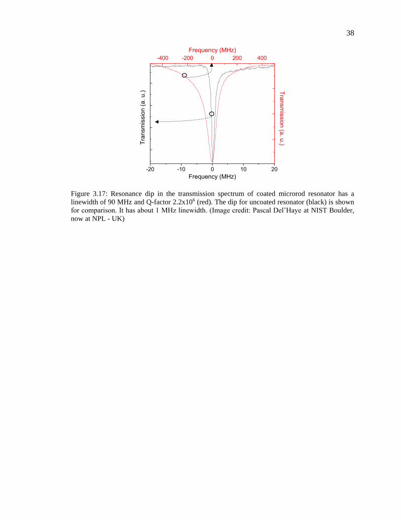
38
Figure 3.17: Resonance dip in the transmission spectrum of coated microrod resonator has a
linewidth of 90 MHz and Q-factor 2.2x10⁶ (red). The dip for uncoated resonator (black) is shown
for comparison. It has about 1 MHz linewidth. (Image credit: Pascal Del’Haye at NIST Boulder,
now at NPL - UK)
-20 -10 0 10 20
Tra
nsm
issio
n (
a.
u.)
Frequency (MHz)
-400 -200 0 200 400
Tra
nsm
issio
n (a
. u.)
Frequency (MHz)

39
CHARACTERIZATION OF THIN FILMS ON OPTICAL FIBERS
4.1 Introduction
The standard method to characterize thickness and refractive index of thin films is
ellipsometry. But performing ellipsometry on highly curved surfaces such as an optical
fiber with good resolution is challenging with conventional ellipsometers. Devices with
high lateral resolution about 10 µm and high accuracy of measurement have been reported
in literature. However most of them are "state-of-the-art" rather than commercial devices.
Micro-ellipsometers designed to examine samples with flat surface could be used for
curved surfaces, if the lateral resolution is high enough allowing a part of the cylindrical
surface to be considered as planar. Some micro-ellipsometers are developed to measure
optical parameters of rough or curved surfaces but the output optical signal is difficult to
interpret. Moreover it would need correct model to perform ellipsometric measurement
even if an appropriate ellipsometric device is at our disposal. Imaging ellipsometers, on the
other hand, have a higher resolution (1 - 10 um)[27, 28]. The highest lateral resolution of
1 µm available in a commercial device [27], may suffice for measuring film thickness on
an optical fiber but the light reflected from the bottom side of the fiber could pose a
challenge. Efforts are still ongoing to make an imaging ellipsometer for curved surfaces
[29] and several problems have been acknowledged in interpreting the measurement data.
In this chapter, another technique is explored for measurement of film RI and
thickness. The coated fiber is treated as a scatterer and its scattering signature is analyzed
at a given wavelength to extract the thin film properties. The motivation comes from the
fact that Mie scattering of a particle is sensitive to its geometrical and optical properties
and has been used extensively for decades to characterize various scatterers, spinning off

40
several applications including characterization of optical fibers. Presby in his pioneering
work [30] applied scattering from a fiber to determine its diameter and refractive index.
His work was followed by some others related to core-shell systems such as polymer coated
fibers, tapered fibers [31]. However none of these shells can be considered as a thin film.
In this chapter, scattering signatures of the coated fibers presented in Chapter 3 are used to
determine refractive index and thickness of the films. Section 4.2 is an overview of the
theory of light scattering from concentric cylinders, followed by experiment and data
presented in Section 4.3 and 4.4. Data analysis along with results are presented in Section
4.5 where the encountered challenges and alternatives have been presented.
4.2 Theory of Scattering from Layered Fibers
The theory of light scattering from multilayered cylinders was first proposed by
Kerker [32]. A concise review of the theory starting from wave equation up to the scattering
intensity is presented in this section. We begin by identifying the orthonormal set of vector
functions that are solutions to the vector wave equation. These are generated by a scalar
function that satisfies scalar wave equation and a pilot unit vector. Any solution to the
vector wave equation can be expressed as a linear combination of these vector functions.
Thus �⃗� and �⃗⃗� are expressed as a combination this basis set in cylindrical coordinates,
which satisfy Maxwell’s equations. Next, the boundary conditions are derived. To derive
the scattering intensity, all we need is to construct the scalar function in each layer that
generates the field. We begin with the vector wave equation,
2 2 2 0A n k A . (4.1)
It is easy to verify that if is a solution of the scalar wave equation 2 2 2 0n k ,
and a is a constant unit vector, then the following three vector functions satisfy Equation

41
4.1:
L
M a
MN
nk
(4.2)
Below is a quick proof that M satisfies Equation 4.1. Substituting �⃗⃗� into Equation
4.1, we get
2 2 2 2 2 2M n k M a n k a
. (4.3)
Using the identity 2 2A A , RHS of Equation 4.3 becomes
2 2 2a n k a . (4.4)
Taking the curl operator out, we get
2 2 2 0n k a
(4.5)
Since ψ is the solution of scalar wave equation. Hence M (and therefore N )
satisfies vector wave equation.
Note that curl L = 0 and hence cannot satisfy Maxwell’s equations for time
harmonic fields. Therefore, from here we use only M and N .
An important point to note is that all 3 are orthonormal functions and form a basis
set. Any solution to the vector wave equation can be represented as a linear combination
of these vector functions. We will attempt to construct �⃗� and �⃗⃗� from these such that they
satisfy Maxwell’s equations:
E ikH (4.6)
2H ikn E (4.7)
It can be shown that the following combinations of M and N forming �⃗� and �⃗⃗�
satisfy Equations 4.6 and 4.7:

42
v uE M iN (4.8)
u vH n M iN (4.9)
Here subscripts v and u are scalar functions creating the vector solution M or N .
All we need to find is the scalar functions v and u and obtain �⃗� and �⃗⃗� using Equations 4.8
and 4.9. It is easy to verify and also intuitive, that the pilot vector a for a cylinder is z i.e.
unit vector pointing along the cylinder axis. Thus vectors M and N for a cylinder are as
follows.
M z (4.10)
1
M rr r
(4.11)
2
2
1 1 1 1N r r z
nk z r r z r r r r
. (4.12)
Since m , the solution of the scalar wave equation in cylindrical coordinates is of
the form 2 2 2rim i z i tme Z n k e , where m is the azimuthal order, Zm is Bessel function
of any kind, r is radial coordinate, β is propagation constant and ω is angular frequency,
M and N can be further written as,
im
M rr r
(4.13)
2
2
1 1m m m m m
i mN r r z
nk r nkr nkr r r r
. (4.14)
But since satisfies scalar wave equation in cylindrical coordinates which is,
2 2
2 2
2 2 2
1 10r n k
r r r r z
(4.15)
the last term of Equation 4.14 can be simplified. Thus
2 2 2m m m
i mN r n k z
nk r nkr
(4.16)

43
The final expression for �⃗� and �⃗⃗� fields is
im v
E v r inku zr r
(4.17)
im u
H n u r inkvzr r
. (4.18)
Here we pause for an important observation. Note that for u=0, �⃗⃗� has only z
component while E is in the transverse plane of the cylinder. This mode is called the TE
mode. While for v = 0, �⃗� has only z component while �⃗⃗� is in transverse plane which is the
TM mode. This is the consequence of β being 0. For non-zero β, the modes cannot be
separated. This dissertation is all about normal incidence to the fiber or β=0. Now for
concentric cylinder case, we construct u and v and use that to obtain coefficients an and bn
for multilayered cylinder and obtain intensity at infinity. Before doing that we need
boundary conditions simplified in terms of u and v.
Boundary Conditions: For dielectric cylinder such as a fiber, tangential components
(z and φ) of �⃗� and �⃗⃗� fields will be continuous. Therefore the boundary conditions
following from Equations 4.17 and 4.18 are:
1 1
1
2 21 1
11
i i i i
i i
i i i i
i ii i
n u n u
v v
r r
n v n v
u un n
r r
(4.19)
The expression for u for a single layered cylinder with core radius a and cladding
radius b can be written as follows, as derived in [32].

44
00 0
1 11 1
22
,
,
.
m m m m
m
m m m m m
m
m m m
m
r b u F J n kr b H n kr
b r a u F B J n kr b H n kr
r a u F B J n kr
(4.20)
Here 1m im i t
mF e and 0n , 1n and 2n are refractive indexes of outer medium,
layer and core respectively. The 4 boundary conditions applied each interface yield 4
equations relating coefficients of adjacent regions. Applying crammers rule yields the
scattering coefficient:
' ' '1 1 2 1 1 2 2 2 2
1 2 1 2 2 2
' ' '1 1 1 1 1 1 0 0 1
1 ! 1 1 0 10
' ' '1 1 2 1 1 2 2 2 2
1 2 1 2 2 2
' ' '1 1 1 1 1 1 0 0 1
1 ! 1 1 0 1
0
0
0
0
0
0
0
0
m m m
m m m
m m m
m m m
m
m m m
m m m
m m m
m m m
n H n n J n n J n
H n J n J n
n H n n J n n J n
H n J n J nb
n H n n J n n J n
H n J n J n
n H n n J n n H n
H n J n H n
(4.21)
Here 2 ka and 1 kb . This is similar in form to equation 5.1.28 in Kerker’s book
[33] for multilayered sphere, though not apparent at first look. On replacing Hankel
function in the first column by J+iY, and splitting the determinant into two - D1, D2, first 2
columns of D1 become identical thus vanishing D1, while D2 takes the form of 5.1.28 except
that spherical functions , and are replaced by cylindrical functions J, Y and H
respectively. This similarity is not surprising because, for normal incidence, cross section
of a cylinder is similar to equatorial plane of a sphere.
The calculation of scattering coefficients in already implemented in MatScat code
[34] and used in this dissertation with only minor adaptations.
Next section presents experimental details to obtain the scattering pattern to which

45
best-fit theoretical patterns will be found using MatScat.
4.3 Experiment
To determine the film thickness and refractive index of SiNx and SiO2, four strands
of Corning SMF28 were coated with single layer of SiNx and four others with SiO2. SMF
was chosen for its better axial uniformity compared multimode fibers from Thorlabs.
Deposition times for SiNx are 10, 21, 30 and 40 mins while 3, 4, 5 and 6 mins for SiO2
which grows faster.
A simple scatterometer was set up to obtain scattering pattern of the coated fibers
to determine layer thickness and refractive index from the pattern. The set up schematic
shown in Figure 4.1 consists of a HeNe laser (<1 mW), polarizer, beam splitter, Newport
rotation stage, computer controlled stage controller, detector with pinhole mounted on a
rigid metal arm 9-10 inch long while the arm is attached to the rotation stage. Optical limit
switch of the stage was disabled to allow 360 degree rotation. At the center of the stage,
the fiber is placed perpendicular to the beam and the stage. Fiber is secured in a chuck held
in a holder screwed to a kinematic mount glued to lab jack (Figure 4.2). Kinematic mount
is necessary to align the fiber perpendicular to the beam and rotation stage while lab jack
is used to adjust the height of the fiber to probe different regions. The mounted fiber is
placed at the center of the stage. Rotation stage is held at an elevation such that beam
height and detector coincide.

46
Figure 4.1: Schematic of experimental set-up. BS: Beam Splitter, PDA: Photodiode Amplifier, DAQ: Data
Acquisition card. Computer controls the rotation stage and scattering signal is read through the DAQ.

47
Figure 4.2: Scatterometer for fiber characterization.
The normally incident HeNe beam polarized parallel (TM) or perpendicular (TE)
to the fiber axis is scattered off the fiber generating a pattern and the detector collects the
scattering signal. A generated pattern for SMF28 can be seen in Figure 4.3 showing
photograph of scattering of TM polarized HeNe on a circular screen with an entry hole for
beam. Portion of the long fiber hit by beam is marked as fiber. Almost symmetric
backscattering with a sharp cut-off can be seen on either side of the beam entry hole. Axial
uniformity of the fiber can be gauged from the straightness of the fringes in the pattern. If
uniform, the fringes will be aligned with the fiber axis like in this picture of SMF. Thorlabs
fibers forms curved or tilted fringes generally and necessitates using a pinhole, while for
SMF, a simple slit can be attached to the detector head for appropriate resolution.
When sweeping across backscattering, the detector (~1.5” wide) blocks the beam
Detector
Arm
Rotation Stage Fiber
Chuck
Fiber Mounting mechanics

48
clipping data between scattering angles 175 – 180 degrees (measured from incident
wavevector �⃗� ) which makes sense as the detector arm is about 9” long.
Figure 4.3: Scattering of polarized HeNe (E || fiber) from a fiber on a circular screen with an entry
hole for beam. Portion of the fiber hit by beam is marked as fiber. Backscattering pattern can be
seen with beam entry hole at the center.
4.4 Scattering Data for Single Layered Fiber
FT200EMT: Data for FT200EMT were collected with a pinhole mounted on the
detector. Backscattering patterns of ZN7, ZN8, ZN9, and ZN10 coated with SiNx with
increasing deposition times (see Figure 3.4 for optical images) are given in Figure 4.4 -
Figure 4.7. For each fiber, data was collected at 90 degree intervals around the fiber giving
4 patterns. Since the pattern is theoretically symmetric about the incident wavevector, it
has been overlapped about the symmetry line in these figures. A good overlap is indicative
of symmetry of the coated fiber. Any deviations are due to non-uniformity of core fiber,
coated film or both. Out of these 4 fibers, overlap of ZN8 (Figure 4.5) is the best.
Fiber
Circular screen
k

49
Figure 4.4: Normalized backscattering patterns of FT200EMT coated with ~50 nm layer [ZN7],
taken at 90⁰ azimuthal intervals. Two patterns (red and black) in each plot are data about
symmetry axis i.e. incident beam.
Figure 4.5: Normalized backscattering patterns of FT200EMT coated with ~100 nm layer [ZN8],
taken at 90⁰ azimuthal intervals. Two patterns (red and black) in each plot are data about
symmetry axis i.e. incident beam.
150 155 160 165 170 175
0
1
150 155 160 165 170 175
0
1
150 155 160 165 170 175
0
1
150 155 160 165 170 175
0
1
150 155 160 165 170 175
0
1
150 155 160 165 170 175
0
1
150 155 160 165 170 175
0
1
150 155 160 165 170 175
0
1
Scattering Angle [deg]
150 155 160 165 170 175
0
1
150 155 160 165 170 175
0
1
150 155 160 165 170 175
0
1
150 155 160 165 170 175
0
1
Scattering Angle [deg]

50
Figure 4.6: Normalized backscattering patterns of FT200EMT coated with ~250 nm layer
[ZN9], taken at 90⁰ azimuthal intervals. Two patterns (red and black) in each plot are data
about symmetry axis i.e. incident beam.
150 155 160 165 170 175
0
1
150 155 160 165 170 175
0
1
150 155 160 165 170 175
0
1
150 155 160 165 170 175
0
1
Scattering Angle [deg]

51
Figure 4.7: Normalized backscattering patterns of FT200EMT coated with ~500 nm layer
[ZN10], taken at 90⁰ azimuthal intervals. Two patterns (red and black) in each plot are data
about symmetry axis i.e. incident beam.
Corning SMF28: Scattering patterns of ZN19, ZN17, ZN20, ZN21 coated with
SiNx (see Figure 3.5 for their optical image) are shown in Figure 4.8. Compared to the
patterns of FT200EMT, these patterns are more spread out with broader fringes. This is
due to smaller diameter to wavelength ratio that provides shorter optical path length
compared to FT200EMT almost double the size of SMF.
Note that the pattern for fiber with deposition time 21 minutes is very different from
other three. This is because ZN19, ZN20 and ZN21 with deposition times 10,30,40 mins
were prepared with Corning SMF28e+ supplied by Fiber Instrument Sales Inc. while ZN17
with deposition time 21 mins was made with fiber from an old spool of SMF. Samples of
bare fiber from this spool when characterized had a slightly higher RI than expected for
silica.
150 155 160 165 170 175
0
1
150 155 160 165 170 175
0
1
150 155 160 165 170 175
0
1
150 155 160 165 170 175
0
1
Scattering Angle [deg]

52
Figure 4.8: Normalized backscattering patterns of SMF28 coated with silicon nitride for 10-40
mins (Fiber ID’s are ZN19, ZN17, ZN20, ZN21 respectively).
Due to high uniformity of the bare SMF28e+, LHS and RHS patterns overlap much
better for coated fibers than those of Thorlabs (Figure 4.4 - Figure 4.7). An example of
spectacular overlap of a coated SMF28e+ can be seen in Figure 4.9.
0
1
150 155 160 165 170 175
0
1
0
1
0
1
10min
Scattering Angle [deg]
40min
21min
30min

53
Figure 4.9: LHS-RHS overlap of backscattering of ZN19 prepared using Corning SMF28e+.
Another set of fibers (Fiber ID: ZN25, ZN26, ZN18, ZN24) was coated with silica
for 3, 4, 5 and 6 minutes respectively. As mentioned earlier, these fibers do not exhibit
iridescent colors due to low index contrast between fiber (fused silica) and film (PECVD
silica). See Figure 3.6 for a representative optical image of silica coated fiber. Normalized
backscattering patterns for these 4 fibers are shown in Figure 4.10. The fringe contrast is
lower than that for SiNx coated fibers.
150 155 160 165 170 175
0.0
0.2
0.4
0.6
0.8
1.0
No
rma
lize
d In
ten
sity
Scattering Angle (deg)
LHS
RHS

54
Figure 4.10: Normalized backscattering patterns of SMF28 coated with silica for 3-6 mins.
(Fiber ID’s are ZN25, ZN26, ZN18, ZN24 respectively)
4.5 Data Analysis
4.5.1 Algorithm for Characterization of Fibers
The Matlab code – MatScat [34] implementing the theory of light scattering from
concentric cylinders was adapted to determine the unknown refractive index and thickness
of the coated fibers. The program takes in a set of radii 1 2, , , Nr r r and refractive
indexes 1 2, , , Nn n n for N concentric cylinders and calculates the scattering pattern in
far field for any polarization and wavelength. In this work, a brute-force search was used
to characterize the coated fibers, a system of concentric cylinders essentially. The search
time can be reduced by predetermining the refractive index of the core fiber on which layer
is coated. The procedure to characterize the index and thickness of layers and bare fiber
refractive index and diameter is explained below.
150 155 160 165 170 175
0
1
150 155 160 165 170 175
0
1
150 155 160 165 170 175
0
1
150 155 160 165 170 175
0
1
3 min
4 min
5 min
Scattering Angle [deg]
6 min

55
Bare Fiber: For a bare or uncoated fiber, N = 1 and only unknowns to be determined
are r1 - the radius of the fiber and n1 - its refractive index. To find r1 and n1, a 2 dimensional
search space of radius and index is created. The search space for fiber radius and index
consists of Mr and Mn odd elements respectively. If tolerance specification of the fiber is
10r r , then the search space Sr for radius consisting of Mr elements is
10 10 10 10, , 2 , ,r r rS r r r r r r r r where2
1r
r
r
M
. Similarly search space Sn
is 10 10 10 10,n ,n 2 , ,n n nS n n n n n n where2
1n
n
n
M
. Theoretical
backscattering pattern is generated for each pair {Sr(i), Sn(j)} where i and j are element
index in each set. The peak of generated theoretical pattern is normalized to 1 (denoted as
,i j ) and compared to similarly normalized experimental data by summing the
squares of the differences between theory and experimental data ( 2
, ,i j i j ).
This gives a 2D map of .The value , min ,I J i j is the Least Square Error (LSE)
and { ,r nS I S J } are the radius and refractive index of the bare fiber. This procedure can
be applied to data taken from different segments of fiber from the spool to confirm the
value of refractive index (nco) of the fiber.
Coated Fiber: A coated fiber has 2 concentric cylinders consisting of the core and
the film. Here N = 2 and hence it is a 4 dimensional search space. But using nco from bare
fiber characterization, it reduces to 3D space of 1 2r n tM M M elements. Search range for
fiber radius is still 10r r , while that of film index and thickness is 20 2n n and 0t t
respectively. Here 0t is the guessed thickness guided by SEM (see APPENDIX C) and t
is chosen within 5-10% of 0t . Choice of 20n was made based on the observation that

56
transmission spectrum of Bragg fibers fabricated assuming unchanged had shifted to that
corresponding to higher refractive index.
Error is calculated in the 3 dimensional space of r1, n2 and t. Finding the global LSE
gives the root { 1 2, ,r n tS I S J S K } where K is the index of thickness value corresponding
to LSE. Thus the fiber diameter, film refractive index and thickness are determined at the
location of beam on the fiber. The execution time of the code depends on the granularity
of the search space which should be chosen wisely.
4.5.2 Results
4.5.2.1 Bare Fiber
Before moving onto characterization of films, it is helpful to first characterize the
bare (uncoated) fiber to pre-determine the refractive index of its material. Once the material
index is known, it can be assumed to be constant throughout the spool with only the
diameter varying within the tolerance specification. Both FT200EMT and SMF28 were
characterized by light scattering using the algorithm in Section 4.5.1. Scattering data were
collected at 3 different times without disturbing the fiber to ensure the repeatability
simultaneously.
LSE method was used to find refractive index and diameter using backscattering
signal (150⁰ -175⁰) on either side of the beam. Retrieved n1 and r1 from the two sides were
averaged. Table 1 shows the results for FT200EMT performing this procedure 3 times
separated by about 5 minutes.

57
Table 1: Calibration of Bare FT200EMT using backscattering.
Time 1 Time 2 Time 3
Left Right Right Left Left Right
n 1.4575 1.4569 1.4569 1.4573 1.4575 1.4569
D [µm] 201.35 201.85 201.85 201.60 201.35 201.85
Mean n=1.4572,
D=201.60
n=1.4571,
D=201.72
n=1.4572,
D=201.60
Note that n and t retrieved from one side (left or right) are quite consistent with time. The
mean value of refractive index at each time is very close to that provided by Thorlabs
technical support (n= 1.457173023) and the diameter is also within the specification of
core diameter - 200 ± 5 µm [35].
Corning SMF28 was characterized similarly. However it is not a single cylinder
like FT200EMT. Geometrically speaking, it is a set of 2 concentric cylinder – an outer
cladding of diameter 125 µm and an 8 µm core embedded at the center. First the effect of
the core on the scattering pattern was investigated theoretically. Figure 4.11 shows the
difference between patterns with and without core exhibiting negligible difference except
in the range 0⁰ – 10⁰ and 175⁰ – 180⁰. Therefore core is neglected altogether for SMF28
in all subsequent work and any data in this range was truncated for analysis.

58
Figure 4.11: Difference between theoretical scattering patterns generated with the core and
without the core.
This analysis simplified the model for SMF28 to a single rod of diameter 125 µm.
Now its refractive index was found by the same method as for FT200EMT. Table 2
summarizes the results for SMF28 characterization.
Table 2: Calibration of Bare SMF28 using backscattering
Time 1 Time 2 Time 3
Left Right Right Left Left Right
n 1.4572 1.4567 1.4565 1.4574 1.4572 1.4567
D [µm] 125.098 125.119 125.133 125.077 125.098 125.119
Mean n=1.4570,
D=125.108
n=1.4570,
D=125.105
n=1.4570,
D=125.108

59
The mean refractive index of the cladding was consistently 1.457 despite neglecting the
core while the diameter is also with the specifications provided by Corning. This result
further validates the fact that effect of core on backscattering is limited only within 175⁰ -
180⁰. Representative backscattering patterns of bare FT200EMT and SMF28e+ can be
seen in Figure 4.12 with denser fringes for FT200EMT as noted earlier.
Figure 4.12: Normalized backscattering patterns of Thorlabs FT200EMT (red) and Corning SMF28e+
(blue).
4.5.2.2 Coated Fiber
Method described in Section 4.5.1 was followed to find the film RI, film thickness
and fiber diameter from the best-fit pattern. Table 3 tabulates the resultant film parameters
for SiNx coated fibers along with the search window limits and LSE. LSE variation with
150 155 160 165 170 175
0.0
0.2
0.4
0.6
0.8
1.0
Bare SMF
No
rma
lize
d In
ten
sity
Scattering Angle (deg)
150 155 160 165 170 175
0.0
0.2
0.4
0.6
0.8
1.0
Bare TL
No
rma
lize
d In
ten
sity
Scattering Angle (deg)

60
diameter axis is plotted in Figure 4.13.
Table 3: Result for SiNx Root Search using backscattering
Fiber ID Search Range Root
n t [nm] d [µm] n t
[nm]
d [µm] LSE
ZN19 2.1 – 2.7 200 – 300 124.4 – 125.6 2.492 224 125.07 0.98
ZN17 2.3 – 2.8 475 – 525 124.3 – 125.7 2.482 502 124.99 0.65
ZN20 2.1 – 2.7 702 – 858 124.5 – 125.5 2.457 788 124.74 1.86
ZN21 2.2 – 2.8 1045 – 1155 124.3 – 125.7 2.497 1056 125.17 8.35
Figure 4.13: LSE vs Fiber Diameter for SiNx coated fibers.
Some of the six valleys present in these graphs have competing LSEs, something
to be wary of. The impact of such periodic LSE has been investigated in Section 4.5.3.
Similar results for SiO2 coated fibers are present in Table 4 and Figure 4.14.
124.4 124.6 124.8 125.0 125.2 125.4 125.6
10
15
20
25
30
35
124.4 124.6 124.8 125.0 125.2 125.4 125.6
1
2
3
4
5
124.4 124.6 124.8 125.0 125.2 125.4 125.6
012345678
LS
E
ZN21 LSE
LS
E
ZN19 LSE
LS
E
Diameter (um)
ZN17 LSE

61
Table 4: Result for SiO2 Root Search using backscattering.
Fiber ID Search Range Root
n t [nm] d [µm] n t
[nm]
d [µm] LSE
ZN25 1.2 – 1.8 798 – 882 124.3 – 125.7 1.479 874 124.6 0.22
ZN26 1.3 – 1.7 1045 – 1155 124.3 – 125.7 1.464 1095 124.5 0.42
ZN18 1.4 – 1.6 1330 – 1470 124.4 – 125.6 1.462 1386 124.5 0.71
ZN24 1.3 – 1.7 1615 – 1785 124.3 – 125.7 1.476 1742 124.6 0.40
Figure 4.14: LSE vs Fiber Diameter for SiO2 coated fibers.
The step-like LSE vs Diameter plot is significantly different from that of SiNx
which was periodic. Additionally the error is smaller than for SiNx most likely due to
similarity in the film RI and fiber RI. This is evident from Figure 4.15 showing the best fit
patterns (red) superimposed on corresponding experimental scattering data (black).
124.4 124.6 124.8 125.0 125.2 125.4 125.6
0.0
0.4
0.8
1.2
1.6
124.4 124.6 124.8 125.0 125.2 125.4 125.6
0.0
0.4
0.8
1.2
1.6
124.4 124.6 124.8 125.0 125.2 125.4 125.6
0.0
0.4
0.8
1.2
1.6
LS
E
ZN25
LS
E
ZN26
LS
E
Diameter (um)
ZN24
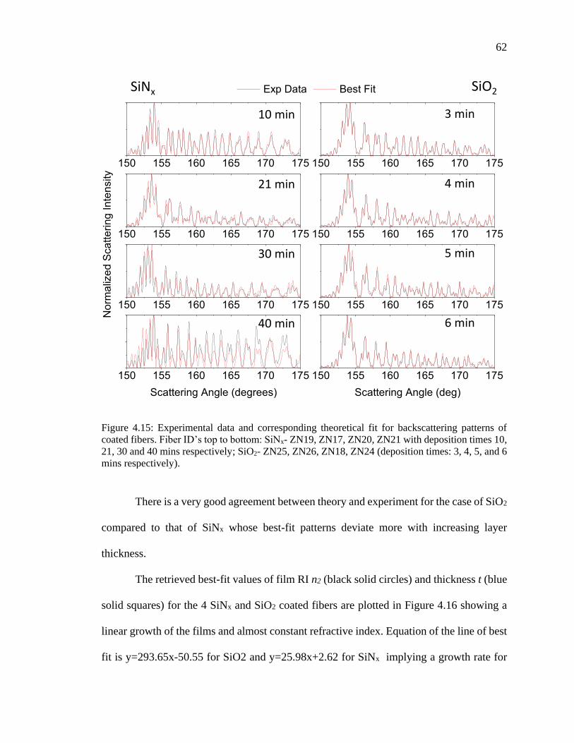
62
Figure 4.15: Experimental data and corresponding theoretical fit for backscattering patterns of
coated fibers. Fiber ID’s top to bottom: SiNx- ZN19, ZN17, ZN20, ZN21 with deposition times 10,
21, 30 and 40 mins respectively; SiO2- ZN25, ZN26, ZN18, ZN24 (deposition times: 3, 4, 5, and 6
mins respectively).
There is a very good agreement between theory and experiment for the case of SiO2
compared to that of SiNx whose best-fit patterns deviate more with increasing layer
thickness.
The retrieved best-fit values of film RI n2 (black solid circles) and thickness t (blue
solid squares) for the 4 SiNx and SiO2 coated fibers are plotted in Figure 4.16 showing a
linear growth of the films and almost constant refractive index. Equation of the line of best
fit is y=293.65x-50.55 for SiO2 and y=25.98x+2.62 for SiNx implying a growth rate for
150 155 160 165 170 175
150 155 160 165 170 175
150 155 160 165 170 175
150 155 160 165 170 175
150 155 160 165 170 175
150 155 160 165 170 175
150 155 160 165 170 175
150 155 160 165 170 175
Exp Data Best Fit
Scattering Angle (deg)
No
rma
lize
d S
ca
tte
rin
g In
ten
sity
Scattering Angle (degrees)
SiNx SiO2
10 min
21 min
30 min
40 min
3 min
4 min
5 min
6 min

63
SiO2 an order of magnitude greater than for SiNx. These growth rates are higher than those
obtained previously for stationary fiber on the platen [22] (Figure 4.17).
The refractive index of SiNx (n=2.49) is also significantly higher than that on flat
wafer. These observations are qualitatively in agreement with [24] as the fiber is at an
elevation from the base where the wafer is placed in conventional usage of PECVD. In
addition to elevation, rotation and geometry of our substrate also contribute to deviation
from film growth characteristics on wafers. Note that these results were obtained under the
assumption of perfect circular geometry, while in practice, the following factors are
potential sources of error: 1) ellipticity of the fibers [25] 2) eccentricity of the 8 µm core,
3) surface roughness of film, film cracks/gaps if present, 4) any eccentricity of fiber and
detector system.
10 15 20 25 30 35 40
1.0
1.5
2.0
2.5
3.0
SiNx Refractive Index
SiNx Thickness
Deposition Time (min)
Re
fra
ctive
In
de
x
200
400
600
800
1000
1200
1400
1600
1800
Th
ickn
ess (n
m)

64
Figure 4.16: Refractive index and thickness as a function of deposition time retrieved from
scattering pattern of the coated fibers. Blue line is the line of best fit while black line is located at
the mean value of refractive index.
3 4 5 6
1.0
1.5
2.0
2.5
3.0
SiO2 Refractive Index
SiO2 Thickness
Deposition Time (min)
Re
fra
ctive
In
de
x
200
400
600
800
1000
1200
1400
1600
1800T
hic
kn
ess (n
m)

65
Figure 4.17: Silicon nitride growth rate curve on stationary fiber (a-b). Reproduced from [22].
A representative error bar was calculated using ZN9 (~11 min deposition of SiNx).
Scattering data at 90 degree intervals around the fiber were used to find the root at each
orientation (Table 5). The mean refractive index is 2.49 and standard deviation is 0.0076
while the mean thickness is 259 nm and standard deviation is 2.4 nm. However with
increasing thickness, the as we saw in Figure 4.15, the pattern starts to become more
asymmetrical indicating increased non-uniformity which would mean higher error for
thicker layers.
metal ring holderbare laser rod
silicon wafer(a) (b)
5 10 15 20 25 30
100
200
300
400
500
Thic
kness (
nm
)
Time (min)
Thickness
Linear Fit of Thickness
Equation y = a + b*x
Weight No Weighting
Residual Sum of Squares
68.64286
Adj. R-Square
0.99845
Value Standard Error
ThicknessIntercept -34.5 10.14713
Slope 19.70408
0.54789
Silicon Nitride

66
Table 5: Root search result for error bar calculation on ZN9
Orientation Angle [deg] n2 t [nm]
0 2.49 260
90 2.48 256
180 2.50 257
270 2.49 261
<n2> = 2.49, SD = 0.0076 <t> = 258.6, SD = 2.4283
For validation of the results, thicknesses retrieved by scattering were compared to
those obtained from SEM of coated fibers (Figure 4.18) fabricated using FT200EMT
(APPENDIX C) [25].
In Figure 4.18 (a), SiNx thicknesses retrieved by Mie scattering and SEM are plotted
together. Fibers used for SEM are ZN9, ZN11, ZN12 and ZN13. The deposition time and
measured thickness is tabulated in Table 6. These were made 2 years before the 4 fibers
used for scattering based characterization. The values obtained from scattering are located
close to the SEM calibration line in red. In fact, there is a small positive offset in the
thicknesses obtained by scattering from the calibration line. This could be due to either
different growth on FT200EMT (used for SEM) than on SMF28 or some other change in
the calibration of the PECVD tool itself over the years which was stood unused for a long
time.

67
Figure 4.18: Growth rate obtained using Scattering compared to that obtained from SEM. Left:
SiNx; Right: SiO2.
0.0
0.5
1.0
1.5
2.0
2.5
3.0
0 20 40 60 80 100 120
SEM
Linear Fit of SEM
Thic
kn
ess (m
)
Adj. R-Square0.99983
Value Standard Error
ThicknessIntercept -50.16 12.19
Slope 26.54 0.20
Mie
Deposition Time (min)
3 4 5 6
1.0
1.5
2.0
2.5
3.0
SiO2 Refractive Index
SiO2 Thickness
Deposition Time (min)
Re
fra
ctive
In
de
x
200
400
600
800
1000
1200
1400
1600
1800
Th
ickn
ess (
nm
)

68
Table 6: Scattering vs SEM results for SiNx
Deposition
Time [min]
(on SMF)
Thickness
[nm]
Scattering
Deposition Time
[min]
(on FT200EMT)
Thickness
[nm]
SEM
10
[ZN19]
291 10.82
[ZN9]
251
10.82
[ZN9]
260 29
[ZN11]
704
20.14
[ZN10]
515 39
[ZN12]
984
21.1
[ZN17]
502 112.81
[ZN13]
2947
30
[ZN20]
788
40
[ZN21]
1056
Table 7: Thickness
characterization by scattering
for SiO2
Deposition
Time [min]
Thickness
[nm]
Scattering
3
[ZN25]
861
4
[ZN26]
1094
5
[ZN18]
1386
6
[ZN24]
1742
As a sanity check, the fiber with deposition time 10.82 mins (ZN9) was also
characterized by Mie scattering. The thickness obtained is 260 nm, deviating 4% from
growth rate curve (red) obtained by SEM (APPENDIX C).
A similar comparison between SEM and scattering results for SiO2 coated fibers is
shown in Figure 4.18 (b). The SEM calibration line was obtained from a single
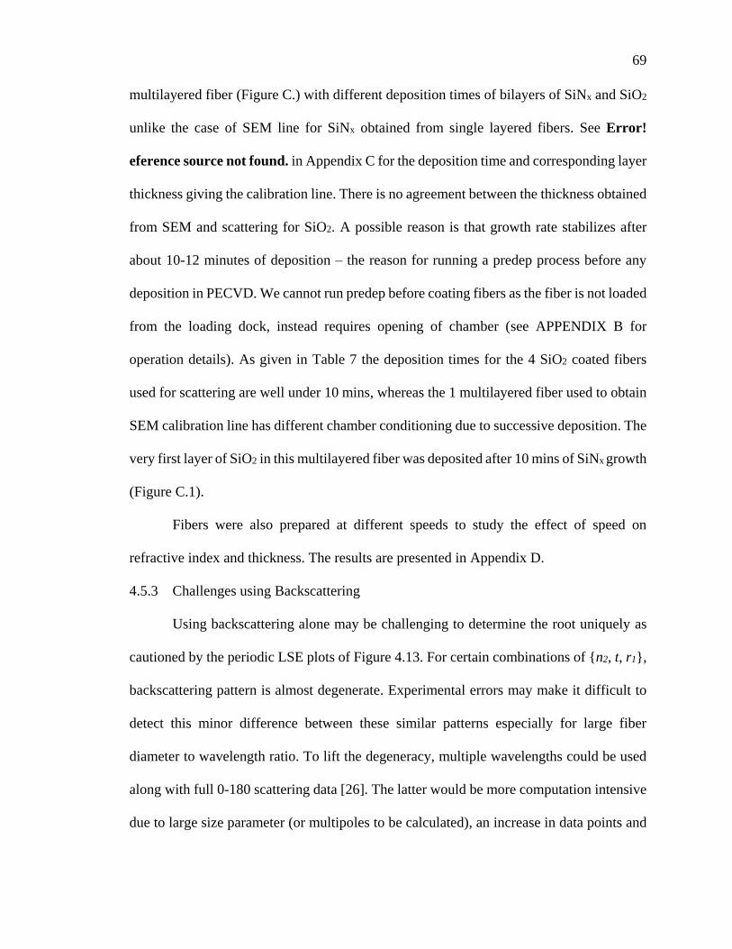
69
multilayered fiber (Figure C.) with different deposition times of bilayers of SiNx and SiO2
unlike the case of SEM line for SiNx obtained from single layered fibers. See Error!
eference source not found. in Appendix C for the deposition time and corresponding layer
thickness giving the calibration line. There is no agreement between the thickness obtained
from SEM and scattering for SiO2. A possible reason is that growth rate stabilizes after
about 10-12 minutes of deposition – the reason for running a predep process before any
deposition in PECVD. We cannot run predep before coating fibers as the fiber is not loaded
from the loading dock, instead requires opening of chamber (see APPENDIX B for
operation details). As given in Table 7 the deposition times for the 4 SiO2 coated fibers
used for scattering are well under 10 mins, whereas the 1 multilayered fiber used to obtain
SEM calibration line has different chamber conditioning due to successive deposition. The
very first layer of SiO2 in this multilayered fiber was deposited after 10 mins of SiNx growth
(Figure C.1).
Fibers were also prepared at different speeds to study the effect of speed on
refractive index and thickness. The results are presented in Appendix D.
4.5.3 Challenges using Backscattering
Using backscattering alone may be challenging to determine the root uniquely as
cautioned by the periodic LSE plots of Figure 4.13. For certain combinations of {n2, t, r1},
backscattering pattern is almost degenerate. Experimental errors may make it difficult to
detect this minor difference between these similar patterns especially for large fiber
diameter to wavelength ratio. To lift the degeneracy, multiple wavelengths could be used
along with full 0-180 scattering data [26]. The latter would be more computation intensive
due to large size parameter (or multipoles to be calculated), an increase in data points and

70
normalization of data to theory. In this section, degeneracy of backscattering patterns for
bare fibers in investigated by displaying scattering patterns for first two diameter values
that best fit the experimental data.
Methods & Parameters: Refractive index of bare fiber was fixed to 1.457 and search
range for core diameter is chosen between 124.3 - 125.7 µm. First two local minima (1st-
red, 2nd-black) are circled in Figure 4.19. Scattering patterns corresponding to these
diameters are shown in the lower 2 subplots. These graphs are corresponding to data taken
for two orthogonal orientations of the fiber. It is difficult to tell which diameter gives a
closer fit to the experimental data. LSE is not a reliable indicator of similarity for such a
close match. Even though the difference between these diameters is less than a micron, it
matters when the fiber is coated with thin film. A diameter off by few hundred nanometers
can lead to error in best fit film parameters.

71
Figure 4.19: Apparent degeneracy in backscattering patterns of SMF28. (a) and (b) are for two
orthogonal orientations of the fiber.
4.5.4 Alternatives
Due to the apparent degeneracy in the backscattering patterns, uniqueness of root
using other scattering regions was investigated numerically. The simplest case of bare fiber
was studied. Theoretical pattern for bare fiber with 2r1 = 125 µm and n1 = 1.457 was
124.4 124.6 124.8 125.2 125.4 125.6 125.8124.2
150 155 160 165 170 175
150 155 160 165 170 175
0
0
6
12
0
1
1
D=124.68
D=125.13
Scattering Angle [deg]
Best FitExperiment
Diameter D [um]
No
rmal
ized
Sca
tter
ing
Inte
nsi
tyEr
ror
125.0
124.4 124.6 124.8 125.2 125.4 125.6 125.8124.2
150 155 160 165 170 175
150 155 160 165 170 175
0
0
5
10
0
1
1
15
D=125.54
D=125.10
Scattering Angle [deg]
Best FitExperiment
Diameter D [um]
No
rmal
ized
Sca
tter
ing
Inte
nsi
tyEr
ror
125.0
(a)

72
assumed to be experimental data for which best fit parameters are to be found. Patterns for
2r1 in the range 125 ± 0.7 µm were compared to this. Error was plotted against 2r1 for 3
scattering regions: 1) backscattering (150⁰ – 180⁰), 2) forward scattering (5⁰ – 20⁰) and 3)
entire pattern (0⁰ – 180⁰). As shown in the top plot of Figure 4.20, the error plot is periodic
for backscattering with 7 valleys, while that of forward scattering (middle) has an
unambiguous unique root though gives an impression of increased period of about 1.2 µm.
In contrast, the bottom graph using entire scattering has no nuance of periodicity and also
has a unique root.
Diameter [µm]
Figure 4.20: Error plot for different scattering regions. Top: 150⁰ – 180⁰, Middle: 5⁰ – 20⁰, Bottom:
0⁰ – 180⁰.

73
Figure 4.21: 2D error plot for coated fiber for forward and backscattering regions.
Similar analysis for coated fibers is shown in the form of 2D plots in Figure 4.21.
It shows theoretical 2D error plot for a hypothetical coated fiber with diameter 125 µm,
film RI = 2.4 and film thickness = 500 nm. Every point on the film thickness vs film RI
plot is error between pattern of this hypothetical fiber and pattern of a fiber with same
diameter but film parameters defined by that point. Lowest error is indicated by red dot
which obviously occurs at RI = 2.4 and thickness = 500 nm. The error plot for
backscattering (150⁰ – 175⁰) on the right has 3 long blue bands or valleys of minima within
the search window. Also the central band containing the root is not as confined compared
to 2D error plot of forward scattering (5⁰ – 20⁰) which has only one blue valley with a well
confined root in the same search window.
The above analysis indicates that in order to obtain a unique root unambiguously,
portion of forward scattering (e.g. 5⁰ – 20⁰) or entire scattering could be used. Next section
presents full scattering data from 10⁰ – 175⁰ for fibers coated with SiNx followed by 3D
root search for one of them to see if that helps.
4.5.4.1 Full Scattering Data
The data presented in the previous sections so far were limited to backscattering
26
5⁰ - 20⁰ 150⁰ - 175⁰
Film Refractive Index n2
Thic
kn
ess
(µm
)
Film Refractive Index n2
Thic
kn
ess
(µm
)

74
region i.e. from 150⁰ – 175⁰. In this section, a collection of scattering data ranging from
10⁰ – 175⁰ for both TM and TE polarizations are presented (Figure 4.22).
Immediately noticeable feature in these patterns is the symmetry. Corning
SMF28e+ is far more symmetric than Thorlabs FT200EMT. Second is the difference in the
backscattering tail. Pattern with TM polarization has a sharp tail while that for TE is more
rounded off in accordance with observation by Marcuse and Presby [36] for bare fibers. In
addition, coated fibers exhibit a larger backward to forward scattering ratio than the bare
fiber counterparts. The fiber with thickest coating – ZN21 (see Figure 3.5 for image), has
the most asymmetric and distorted pattern. It may be due to mechanical flaw in the thick
coating.
TM (E || Fiber) TE (E Fiber)
Uncoated FT200EMT
Uncoated SMF28e+
0
30
60
90
120
150
180
210
240
270
300
3300
30
60
90
120
150
180
210
240
270
300
330
0
30
60
90
120
150
180
210
240
270
300
330
0
30
60
90
120
150
180
210
240
270
300
330

75
Figure 4.22, continued
ZN19
ZN17
ZN20
ZN21
Figure 4.22: Full Scattering Data for coated fibers. See Figure
3.5 for complete fiber recipes.
4.5.4.2 Data Analysis
In this section, results for 3D root search using full scattering data of ZN20 for TM
0
30
60
90
120
150
180
210
240
270
300
330
0
30
60
90
120
150
180
210
240
270
300
330
0
30
60
90
120
150
180
210
240
270
300
330
0
30
60
90
120
150
180
210
240
270
300
330
0
30
60
90
120
150
180
210
240
270
300
330
0
30
60
90
120
150
180
210
240
270
300
330
0
30
60
90
120
150
180
210
240
270
300
330

76
polarization are presented. Ideally full scattering data should be available from 0⁰ - 180⁰.
But due to very strong intensity close to 0⁰ (|| incident beam) and blocking of ∓5⁰ of
backscattering (anti || incident beam), we restrict the data to 10⁰ - 175⁰. This is also the
region where 8 µm core has negligible effect on the pattern. Therefore theoretical scattering
pattern {Iith} considered is also restricted to 10⁰ – 175⁰. The scale of the experimental and
theoretical patterns is equalized by area normalization. Area of experiment/theory
scattering pattern (Ae or At) = sum (Iiexp(th) (θ ϵ [10⁰, 175⁰]))*Δθ. Theoretical pattern was
calculated for same {θi} as experimental. Hence Δθ is equal for both. Before calculating
Least Square Error (LSE), the area of the theoretical pattern (At) is normalized to the area
of experimental data (Ae): Normalized_Iith = Iith/(At/Ae). A 3D root-search is conducted in
the search space of parameters {nlayer,tlayer,dcore} where n is refractive index, t is thickness
and d is diameter. The search range {tlayer} is dictated by SEM growth rate obtained from
calibration fiber, while {dcore} is given by tolerance spec of the fiber. Since RI has increased
[37], we search in a range higher than n expected for flat wafer (n = 2 @ λ=632.8 nm).
Parameters:
Fiber used: ZN20
n0=2.5; %guess layer index d0=125; %guess for variable core diameter (um) t0=0.75; %guess coating thickness (um)
%search range for each dimension dd=0.7; %core diameter variation = +- dd um dn=0.3; %delta index SiN dt=10/100 * t0; %SiN coating thickness variation = +- tt um
%resolution Nd=201; % core dia Nn=31; % layer index Nt=51; % layer thickness
Results:
LSE vs diameter plot obtained from the 3D search: Each point on the graph is the

77
LSE of the 2D n vs t plot at a given diameter.
Figure 4.23: Least Square Error vs Fiber diameter plot for scattering range 10⁰ – 175⁰.
Though not apparent immediately, the average difference between successive local
minima is ~ 0.2 um in Figure 4.23, similar to that for bare fiber using backscattering (Figure
4.13). The local root (n2, t) at each of these minima along diameter axis is given in Table 8
along with corresponding LSE.
Table 8: Root (2r1, n2, t) for 3D search using scattering data 10⁰ – 175⁰.
2r1
Core Diameter
[µm]
n2
(Film RI)
t [µm]
(Film
Thickness)
LSE
124.55 2.28 0.675 2743
124.73 2.42 0.774 2971
124.99 2.24 0.825 3816
125.23 2.78 0.675 4838
125.43 2.28 0.675 2936
125.63 2.52 0.741 4440
124.4 124.6 124.8 125.0 125.2 125.4 125.6
2500
3000
3500
4000
4500
5000
5500
6000
LS
E
Diameter (m)

78
If guided solely by the LSE, the root should be (n2, t) = (2.28, 0.675 µm). However
675 nm is at the edge of the search window t x n2 while according to SEM based calibration,
we expect a thickness around 750 nm. For a more detailed analysis, 2D t x n2 error plots
for the 6 local minima are shown in Figure 4.24. Each plot has a red dot located at the LSE
for that particular plot.
Figure 4.24: 2D error plots of (t x n2) for each local minimum along the 3rd dimension of fiber diameter.
Of all the 6 plots, those with the red dot located at any edge of 2D search space can
be discarded immediately. Thus roots with LSE = {2971, 4440} are the possible candidates.
Out of these, 4440 can be rejected for 2 reasons: (a) LSE is significantly higher (b) lies at
the edge of 3rd dimension – fiber diameter (close to 125.7 µm). Therefore the root (2r1, n2,
t) = (124.73 µm, 2.42, 774 nm). Table 9 summarizes this analysis.

79
Table 9: Root (2r1, n2, t) for 3D search using scattering data 10⁰ – 175⁰.
2r1
Core
Diameter
[µm]
n2
(Film RI)
t [µm]
(Film
Thickness)
LSE Accept/Reject Reason
124.55 2.28 0.675 2743 Reject t at lower
edge
124.73 2.42 0.774 2971 Accept
124.99 2.24 0.825 3816 Reject t at upper
edge
125.23 2.78 0.675 4838 Reject t at lower
edge
125.43 2.28 0.675 2936 Reject t at lower
edge
125.63 2.52 0.741 4440 Reject 2r1 at higher
edge
In conclusion, using scattering pattern from 10⁰ – 175⁰ is also not an independent
method and needs information on thickness. Additionally, one cannot use global minimum.
Valleys of minima occur along the diameter axis (period ~ 200 nm) as well as in n x t plots
using entire scattering and area normalization. Pattern is too intricate to match well given
imperfections deviating scattering from ideal theory for perfectly circular/concentric fiber.

80
MIE SCATTERING OF BRAGG FIBERS
5.1 Introduction
Analysis of scattering of multilayered particles is of great interest for both military
and civil applications. Scattering manipulation by designer particles for invisibility through
scattering suppression [38] and mimicking that of another scatterer, is being studied
extensively. Some theoretical efforts to improve our understanding of scattering from
multilayered spheres include work of Liang et al. [39, 40], in which Mie scattering of Bragg
onion resonators was investigated and Whispering Gallery Modes of the resonator were
mapped to a peculiar scattering behavior. In another theoretical work on scattering of Bragg
spheres [41], enhancement in backward to forward scattering ratio for large core spheres
was reported. In this chapter, its cylindrical counterpart, a Bragg fiber, traditionally used
for transmission, is studied as a scatterer both theoretically and experimentally. Scattering
patterns were obtained for the Bragg fibers fabricated in PECVD. Peculiar features very
different from that of bare fiber scattering were observed and a model was developed to
explain these features.
Section 5.2 presents the experimental scattering data of Bragg fibers ZN4 and ZN5
followed by a model based on ray-tracing and scattering intensity in Section 5.3. A new
scattering angle diagram based on this is presented in Section 5.4. Scattering pattern of
bare fiber and Bragg fibers for both TE and TM polarizations is explained qualitatively
with the help of these diagram.
5.2 Experimental Data
Scattering data collected for Bragg fibers ZN4 and ZN5 are shown in polar plots of
Figure 5.1. Black plots are for TM polarization while blue for TE. Note that the pattern of

81
ZN4 (b) resembles that of bare fiber in Figure 4.22, reproduced in (a) for reference, with a
dominant forward scattering lobe and tail like backscattering. However the forward
scattering lobe is periodically spiky unlike the smooth lobe of bare fiber. The spikes are
shallower for TE polarization. In contrast to the pattern of ZN4, ZN5 (c) exhibits drastic
difference with scattering in the otherwise dead zone of the bare fiber and suppression in
some regions of forward scattering. Pattern from a different point along the fiber axis of
ZN5 (d) in the vicinity of that used for (c) is modified slightly while that taken from far
away point (e) on the fiber that was closer to the chuck holding the fiber during deposition,
is more like bare fiber though with apparent differences. The same spot probed with 532
nm laser instead of HeNe, shows quite a significant difference between the two
polarizations (f). In the following sections, a model is developed to investigate origin of
these difference.
TM TE
(a) SMF28e+ | λ = 632.8 nm
(b) ZN4 | λ = 632.8 nm
0
30
60
90
120
150
180
210
240
270
300
330
0
30
60
90
120
150
180
210
240
270
300
330
0
30
60
90
120
150
180
210
240
270
300
330
0
30
60
90
120
150
180
210
240
270
300
330

82
Figure 5.1, continued
(c) ZN5 | λ = 632.8 nm
(d) ZN5 | λ = 632.8 nm | TM
(e) ZN5 | λ = 632.8 nm | Close to chuck
(f) ZN5 | λ = 532 nm | Close to chuck
Figure 5.1: Polar scattering plots for Bragg Fibers.
0
30
60
90
120
150
180
210
240
270
300
330
0
30
60
90
120
150
180
210
240
270
300
330
0
30
60
90
120
150
180
210
240
270
300
330
0
30
60
90
120
150
180
210
240
270
300
330
0
30
60
90
120
150
180
210
240
270
300
330
0
30
60
90
120
150
180
210
240
270
300
330
0
30
60
90
120
150
180
210
240
270
300
330

83
5.3 Theory and Comparison to Experimental Data
The scattering patterns at first glance seem complicated with high frequency fringes.
However the broader profile of the pattern is simpler to analyze and contains significant
information. To facilitate analysis, scattering data spread out in an XY graph format are
shown in Figure 5.2 for a bare and Bragg fiber. The left and right columns correspond to
TM (E || to fiber axis) and TE (E⊥to fiber axis) polarizations respectively. The intensity
on Y axis has been truncated to make the intricate pattern visible.
Bare fiber patterns (Figure 5.2 (a) and (b)) exhibit well-defined regions of forward
and backscattering separated by a wide dark zone of negligible scattering intensity. The
forward scattering decreases monotonically with scattering angle, while backscattering
appears as a sudden increase in intensity after the dark zone. Patterns for the two
polarizations differ in the sharpness of transition from dark zone to backscattering. TM is
sharper than TE. Origin of these differences will be explained later.
In contrast to the bare fiber, data of the Bragg Fiber ZN5 (Figure 5.2 (c) and (d)) is
apparently chaotic with no distinct forward and backscattering regions. The main
distinctive features in these patterns are: 1) notches followed by drastic suppression in
forward scattering in the band of 0⁰ – 40⁰, 2) enhanced scattering in the otherwise dark
zone of bare fiber, 3) a bump between 130⁰-150⁰ 4) modified backscattering and 5) narrow
dip in scattering around 130⁰.
To explain the origin of these features in Bragg Fiber scattering as well as the
difference between patterns of the two polarizations, we first characterized the film
properties by fitting method like in CHAPTER 4. However due to high number of
concentric cylinders, best-fit pattern was found manually as the unique pattern of Bragg

84
Fiber made the search easier.
Figure 5.2: Scattering data for TM (left) and TE (right) polarizations for bare (green) and Bragg Fiber
ZN5 (blue).
For Bragg fibers, the theoretical scattering pattern is not very sensitive to variation
in core diameter and terminal layer thickness (Figure 5.3) except for minor differences.
Therefore to reduce the search parameters, core diameter was fixed at 200 µm and terminal
layer thickness to 1 µm, respectively, during the fitting.
Figure 5.3: Effect of terminal layer on scattering of TM polarized HeNe from Bragg fiber assuming 12
pairs of SiNx and SiO2 with thicknesses 165 nm and 375 nm respectively while indexes assumed to be
2.49 and 1.6 respectively.

85
The best fit patterns obtainable by manual search shown in Figure 5.4 (b) and (d),
match with the overall profile of experimental data in Figure 5.4 (a) and (c) reasonably
well. The best-fitted layer thicknesses for SiNx and SiO2 are 166 nm and 375 nm,
respectively, which are within the error bar of SEM based growth rate calibration curve
[25]. The best fit refractive index values for SiNx and SiO2 are 2.495 and 1.608,
respectively. These values will be used for theoretical investigation of the origin of these
scattering patterns.
Figure 5.4: Experiment (blue) vs theoretical fit (red) for ZN5. (Left) TM; (Right) TE.
5.4 Scattering Angle Diagram
Now we develop a scattering angle ( sc ) vs incidence angle ( in ) diagram using ray
tracing. Consider the partial ray diagram for the circular cross section in Figure 5.5. A
pencil of rays is incident on the cross section normal to the fiber axis and reflects (blue)
and transmits (green) through the circle obeying laws of reflection and refraction. Incidence
angle of each ray depends on the lateral location from the central axis (black). The ray
incident head on has in = 0 while that displaced from the center by radius has in = 90⁰.
Thus incidence angle of any ray in the bundle lies in the range [0⁰,90⁰] with respect to local
normal at the air-fiber interface.
0 20 40 60 80 100 120 140 160 180 0 20 40 60 80 100 120 140 160 180
Scattering Angle (sc
)
Scattering Angle (sc
)
(a)
(b) (d)
(c)

86
Figure 5.5: Ray diagram through fiber cross section showing only reflected and transmitted rays.
Out of the infinite scattered rays generated by a given incident ray, only the first
three (Figure 5.7 (a)), marked as ray 1, 2, 3 at 1st, 2nd and 3rd interface respectively are
considered. Scattering angle ( )isc of ray i is measured from the incidence direction and is
given by
1180 2sc in , (5.1)
22sc in r , (5.2)
3180 2 4sc in r (5.3)
for each ray. Here r is the refraction angle. The scattering angle diagram for the 3 rays as
a function of incidence angle is plotted in Figure 5.7 (b). From this diagram it is easy to
read out the rays contributing at a given scattering angle. Region of scattering angle 0⁰ –
100⁰ receives rays 1 with in between ~50⁰ – 90⁰ and rays 2 with in from 0⁰ – 90⁰, while
sc ϵ (100⁰ – 150⁰) receives only rays 1 with in roughly between 17⁰ – 40⁰. Backscattering
range 150⁰ – 180⁰ is formed by superposition of rays 1 and rays 3. Rays 3 with at least two
incidence angles contribute at a given scattering angle, a point missed by Presby [30] but
later corrected by Marcuse [42], elucidating the utility of these plots. Note the wrapping of

87
the curve of ray 3 beyond in ~ 85⁰ where sc reaches 180⁰. This cross-over incidence angle
is inversely proportional to RI of fiber. Ray diagram in Figure 5.6 elucidates the cases
where scattering angles is less or greater than 180⁰.
Low Index High Index
Figure 5.6: Scattering angle can exceed 180⁰ for high refractive index.
This diagram is independent of radius of the fiber but depends on the refractive
index. The curve of rays 3 as well as rays 2 depends on the index. The minimum sc for rays
3 also called the cut-off angle, was used to characterize fiber index by Presby. The
information about the fiber diameter is contained in interference between these rays. The
separation between fringes was used to find the diameter of the fiber in [43]. However the
matter at hand is scattering intensity distribution as a function of scattering angle.
Neglecting interference, we simply include the information of intensity of each ray. We
know from Fresnel reflection coefficients, that intensity I of the rays depends on in and
the number of interfaces on their trajectory. If af inR is the angular reflectance of air-
fiber interface, the scattering intensity of the three types of rays is as follows:
1
2
3
,
1 1 ,
1 1 .
af in
af in fa r
af in fa r fa r
I R
I R R
I R R R
(5.4)
Here the subscript af and fa mean air-fiber and fiber-air respectively. Due to reciprocity of
the system, af faR R R and equations 5.4 reduce to the following:

88
1
2
2
2
3
,
1 ,
1 .
in
in
in in
I R
I R
I R R
(5.5)
We will augment the scattering angle diagram in Figure 5.7 (b) with the intensity
information by making line thicknesses of rays 1 – 3 proportional to I1, I2 and I3
respectively resulting in augmented scattering angle diagrams discussed in next sections
for bare and Bragg fibers.
Figure 5.7: Ray diagram and corresponding scattering angle diagram.
5.4.1 Augmented Scattering Angle Diagram for Bare Fiber
We first consider diagram for bare fiber. Figure 5.8 shows augmented scattering
angle diagram for a bare fiber for TM polarization on the left with reflectance inR
plotted below in axis and scattering signature of the bare fiber beside the sc axis. From
the line thicknesses of sc vs in diagram the origin of characteristics of forward-scattering,
back-scattering and dead-zone become evident. For sc ϵ (0,100), strongly scattered rays 1
at grazing incidence interfere with strong near-normally incident rays 2 that monotonically
(a) (b)
rr
r Ray2
Ray1
Ray3 0 20 40 60 800
20
40
60
80
100
120
140
160
180
sc
in
0 20 40 60 800
20
40
60
80
100
120
140
160
180
sc
in
Ray3
(b)

89
decrease in intensity (width of green line i.e. ray 2 is decreasing with incidence angle). This
band forms the dominant forward scattering of bare fiber that reduces in intensity with
scattering angle. For sc ϵ (100, 150) – the dead zone, only contribution is from the weakly
scattered rays 1. Lastly, sc ϵ (150, 180) is the well-known backscattering region where
only weak ray1 and ray3 contribute. Since the rays 3 are weakest due to 3 bounces, the line
thickness has been scaled up 4 times relative to other 2 curves. Note that the minimum of
ray3 curve at about sc = 150 agrees well with the backscattering cutoff angle of the
experimental data along the Y axis. A similar plot for TE polarization shown on the right,
visualizes the effect of Brewster’s angle clarifying the reason for difference in
backscattering cut off.
TM Polarization TE Polarization
Figure 5.8: Augmented scattering angle diagrams of bare fiber for TM (left) and TE (right)
polarizations. Red curve thickness has been scaled 4 times for visibility.
5.4.2 Augmented Scattering Angle Diagram for Bragg Fiber
Now we are ready to create augmented scattering angle diagram for Bragg fiber
and understand its bizarre pattern. Two assumptions are made in this analysis for Bragg
0
20
40
60
80
100
120
140
160
180
0 10 20 30 40 50 60 70 80 900
1
0 10 20 30 40 50 60 70 80 900
10
20
40
60
80
100
120
140
160
180
0 10 20 30 40 50 60 70 80 900.0
0.5
1.01.0 0.5 0.0
0
20
40
60
80
100
120
140
160
180
0 10 20 30 40 50 60 70 80 900.0
0.5
1.0
RR
R
Angle of incidence (in)
R
Angle of incidence (in)
4x 4x

90
fiber. Firstly, since the thickness of the Bragg layer is much smaller than the core radius,
we neglect its thickness for ray tracing and therefore the skeleton of the diagram remains
the same as in Figure 5.7 and assume that the presence of the Bragg layer modifies only
the local reflectance/transmittance at the air-fiber interface. Secondly, since the ratio of
fiber diameter and wavelength (200/0.633) is very large, the Bragg layers can be assumed
to be locally planar. The reflectance from the layers for the two polarizations can be
calculated using best fit values obtained resulting in diagrams in Figure 5.9.
The presence of the wide stopband in reflectance curve, immediately explains the
bizarre signature of the Bragg fiber. Stopband blocks corresponding incident rays from
entering the fiber stripping a portion of forward scattering. These rays reflected with R=1
appear in otherwise dead zone of bare fiber. To facilitate understanding, dashed lines are
drawn on the figure as eye guides while shaded bands have been drawn on the in and sc
axes to trace the effect of stopband (hatched) and first reflectance peak (gray). Note the
suppression of green (rays 2) leads to suppressed forward scattering while enhancement of
blue (rays 1) curve leads to complementary enhancement of scattering, both marked with
hatched shading and are due to complete stopband. Similar pair of suppression and
enhancement can be observed arising from first reflectance peak highlighted traced by gray
shading which is narrower and has R<1. Being narrower, it suppresses/enhances only
narrow portions of scattering as depicted by gray shaded area on the sc axis. The dip in
reflectance curve lying between 20 – 30 degrees traces to spike around sc = 19⁰ and dip at
130⁰. Note that even though red curve (rays 3) is suppressed due to stopband, there is no
significant effect of this on scattering intensity because it is not a monotonic curve.
Therefore scattering arising from rays with incidence angles outside stopband, make up for

91
the suppression.
Figure 5.9: Scattering Angle Diagrams to explain Photonic Bandgap effect in Bragg Fiber ZN5. (a) TM,
(b) TE.
This analysis shows that scattering can be manipulated by controlling stopband
width and location. Enhancement and suppression of scattering at various angular ranges
can be achieved thus. This is illustrated for several Bragg fibers in Figure 5.10. In particular,
a wide stopband starting from zero degree can lead to enhanced backscattering as shown
in first polar plot of Figure 5.10.
0
20
40
60
80
100
120
140
160
180
0 10 20 30 40 50 60 70 80 900
1
0 10 20 30 40 50 60 70 80 900
10
20
40
60
80
100
120
140
160
180
0
20
40
60
80
100
120
140
160
180
0 10 20 30 40 50 60 70 80 900
10
20
40
60
80
100
120
140
160
180
0 10 20 30 40 50 60 70 80 900
1
RR
R
Angle of incidence (in)
R
Angle of incidence (in)
(a) (b)
TM TE
4x 4x

92
Figure 5.10: Polar scattering patterns for several Bragg fiber designs.
No stopband in the reflectance leads to pattern similar to bare fiber with a forward
and backscattering region separated by dead zone. Such is the case for ZN4 as seen in
Figure 5.11. The reflectance curve is similar qualitatively to that of air-glass interface,
however with some ripples and hence the pattern is similar to bare fiber except with some
spikes which occur due to interference in the Bragg layer in passband.

93
Figure 5.11: Scattering angle diagram for ZN4. Scattering data is for TM polarization. Parameters of
Bragg layers are: nSiN=2.49, nSiO=1.6, tSiN=236 nm, tSiO=109 nm. Again, red curve has been scaled
by a factor of 4 for visibility.
More accurate analysis can be done by including the phase of the rays in the model.
Shift in the ray trajectories due to thickness of the coated Bragg layers, neglected in this
study can further improve the accuracy.
94
CONCLUSION AND FUTURE WORK
This work lays the foundation for coating the surface of axis-symmetric WGMRs
in PECVD with layers with a wide range of refractive index, potentially expanding the
capabilities of the current WGMRs in sensing, mode shaping, spectral and dispersion
engineering. The fabrication method is applicable to resonators shaped out of fibers such
as bottle microresonator [44] and SNAP [45] and other cylindrically symmetric geometries
such as NIST’s microrod resonator as demonstrated experimentally in Section 3.3.4.
Microsphere at the tip of a short large-core fiber may also be coated. The Q-factors of
resultant stratified WGMRs can be further improved by lowering H content of SiNx due to
NH3 as suggested in [46] or operating away from the absorption peaks of different bonds
or using N2 instead of NH3.
The focus of this thesis is the simplified case of axis-symmetric WGMR – an optical
fiber. Fibers were coated uniformly in PECVD chamber by rotating them about axis during
deposition. Single layers were deposited for characterization of the films and multiple
layers for fabricating Bragg fibers – the simplest photonic bandgap fibers.
Mie scattering of single layered fibers was used to determine the refractive index
and thickness of the thin films. It is concluded that characterizing thin films on fibers by
scattering alone is challenging due to experimentally indistinguishable patterns
periodically recurring for various combinations of film refractive index and physical
dimensions of the coated fiber. Moreover, scattering is very sensitive to deviation from
ideal circular geometry. Practically fibers can be elliptical, non-concentric if SMF, axially
non-uniform in diameter or all factors present together. Layer coated on such a fiber adds
to the challenge.

95
Most of the work in this dissertation employs backscattering as used in the
pioneering work of Presby. However, regardless of which scattering region one uses –
backscatter, forward or entire pattern, above factors add complexity to finding best fit
pattern. The problem is that different angular regions of the scattering pattern may match
well for different set of fiber parameters yielding same least square error. This makes it
difficult to uniquely characterize the film unless additional information is available to lift
the apparent degeneracy. Therefore prior knowledge of thickness from SEM was used as a
ball-park to guide the root-search for film parameters in this work.
Refractive index obtained thus from scattering of fibers coated with single layer of
silicon nitride with different deposition times was 2.49 for λ = 632.8nm. The experimental
pattern had a remarkable correlation with theoretical pattern for n=2.49, thickness in
agreement with SEM and fiber diameter within tolerance specification. Silicon nitride
deposited by PECVD (a-SiNx:H) using SiH4/NH3 mixture can have refractive index
exceeding 2 – the typical value for stoichiometric Si3N4 at the same wavelength, depending
on NH3 concentration in the mixture. A 20% Ammonia concentration in NH3/SiH4 mixture
has been reported to have RI exceeding 2.5 at 1550 nm [14]. Even though this work uses
gas ratios for regular silicon nitride, other factors such as substrate temperature, fiber
cycling in the chamber, affect the composition and morphology of the films changing RI
as a result. The dynamic substrate cycling through the gradient of temperature can affect
the sticking coefficient of the heavier Si containing radicals. If Si is retained in the film
more than N compared to the case of stationary wafer, the refractive index will be high.
Whether Si content has increased, can be verified by techniques such as micro-Raman or
X-ray photoelectron spectroscopy.

96
The growth rate of silicon nitride were found higher than that on flat wafers using
same recipe. This could be due to changed growth kinetics at the fiber substrate due to
rotation and sample elevation.
For pure scattering based characterization, pattern should be obtained at multiple
close-by wavelengths. The root will be the one with same thickness and fiber diameter at
all wavelengths and approximately the same refractive index. Theoretically Mie scattering
pattern of a coated fiber may be unique for a tuple of [nCore, nLayer, Core diameter, Layer
thickness], however experimental errors make it non-trivial. It will be interesting to study
theoretically if two coated cylinders with different values for any subset of this tuple have
same scattering signature.
Further, scattering of fabricated Bragg fibers was studied and compared to that of
bare fiber. Pattern is dependent on Bragg layer design. The designs with no stopband for
the wavelength have pattern similar to that of bare fiber while those with a wide stopband
have a radically different pattern. The location of the stopband can be used to steer the
scattering suppression in different directions. With tunable PBG, the visibility at an angle may
be controlled.
To use these coated fibers as WGM resonators requires axial confinement despite
theoretical proofs of high Q factors in a cylinder [47]. Sustaining a WGM of high Q factor
in coated fiber without axial confinement is made difficult by the intrinsic non-uniformity
in commercial optical fibers which already reduces the Q factor to a few thousands.
Additional trace of non-uniformity of coated layer will make it more difficult to have a
WGM with respectable Q factor. Therefore, it is imperative to shape the fiber by either
CO2 laser [45] or splicer [44]or some other means before coating it, a subject of future

97
work.
In summary, PECVD tool was adapted for the first time to coat optical fibers
uniformly to make single layered and Bragg fibers. The deposited films were characterized
non-invasively using Mie scattering of films coated on fibers. Additionally, first
experimental data on Mie scattering of Bragg fibers has been reported, only relevant work
on Bragg coatings being [39] on spheres but limited to theory. Furthermore, anomalous
scattering suppression and enhancement from Bragg fiber has been demonstrated and
explained, which can be controlled by the design of the Bragg layers. A change in the PBG
of the Bragg layers would change the scattering pattern. Backward to forward scattering
ratio can also be drastically increased for wide stopband designs as predicted by numerical
results. Further, a method for depositing films with speed-dependent refractive index has
been introduced. It would be interesting to investigate the chemical composition of the film
as a function of rotation speed of the fiber in PECVD to better understand the modified
growth kinetics.

98
REFERENCES
[1] L. G. Guimaraes and H. M. Nussenzveig, "THEORY OF MIE RESONANCES
AND RIPPLE FLUCTUATIONS," Optics Communications, vol. 89, pp. 363-369,
May 1992.
[2] B. R. Johnson, "Theory of morphology-dependent resonances: shape resonances
and width formulas," Journal of the Optical Society of America A, vol. 10, pp.
343-352, 1993/02/01 1993.
[3] Practical Applications of Microresonators in Optics and Photonics vol. 146. Boca
Raton: Crc Press-Taylor & Francis Group, 2009.
[4] R. Yang, A. Yun, Y. Zhang, and X. Pu, "Quantum theory of whispering gallery
modes in a cylindrical optical microcavity," Optik - International Journal for
Light and Electron Optics, vol. 122, pp. 900-909, 2011/05/01/ 2011.
[5] I. Teraoka and S. Arnold, "Enhancing the sensitivity of a whispering-gallery
mode microsphere sensor by a high-refractive-index surface layer," Journal of the
Optical Society of America B, vol. 23, pp. 1434-1441, 2006/07/01 2006.
[6] D. Zhu, Y. Zhou, X. Yu, P. Shum, and F. Luan, "Radially graded index
whispering gallery mode resonator for penetration enhancement," Optics Express,
vol. 20, pp. 26285-26291, 2012/11/19 2012.
[7] V. S. Ilchenko, A. A. Savchenkov, A. B. Matsko, and L. Maleki, "Dispersion
compensation in whispering-gallery modes," Journal of the Optical Society of
America A, vol. 20, pp. 157-162, 2003/01/01 2003.
[8] I. Teraoka and S. Arnold, "Coupled whispering gallery modes in a multilayer-
coated microsphere," Optics Letters, vol. 32, pp. 1147-1149, 2007/05/01 2007.
[9] A. Yariv, Y. Xu, R. K. Lee, and A. Scherer, "Coupled-resonator optical
waveguide:?a proposal and analysis," Optics Letters, vol. 24, pp. 711-713,
1999/06/01 1999.
[10] J. Scheuer and A. Yariv, "Sagnac Effect in Coupled-Resonator Slow-Light
Waveguide Structures," Physical Review Letters, vol. 96, p. 053901, 02/06/ 2006.

99
[11] E. Guillermain, V. Lysenko, R. Orobtchouk, T. Benyattou, S. Roux, A. Pillonnet,
et al., "Bragg surface wave device based on porous silicon and its application for
sensing," Applied Physics Letters, vol. 90, p. 241116, 2007.
[12] P. Yeh, A. Yariv, and A. Y. Cho, "Optical surface waves in periodic layered
media," Applied Physics Letters, vol. 32, pp. 104-105, 1978.
[13] D. Ristić, A. Chiappini, M. Mazzola, D. Farnesi, G. Nunzi-Conti, G. C. Righini,
et al., "Whispering gallery mode profiles in a coated microsphere," The European
Physical Journal Special Topics, vol. 223, pp. 1959-1969, 2014/09/01 2014.
[14] W. Qiu, Y. M. Kang, and L. L. Goddard, "Quasicontinuous refractive index
tailoring of SiNx and SiOxNy for broadband antireflective coatings," Applied
Physics Letters, vol. 96, p. 141116, 2010.
[15] L. Prkna, J. Čtyroký, and M. Hubálek, "Ring microresonator as a photonic
structure with complex eigenfrequency," Optical and Quantum Electronics, vol.
36, pp. 259-269, 2004// 2004.
[16] S. D. Hart, G. R. Maskaly, B. Temelkuran, P. H. Prideaux, J. D. Joannopoulos,
and Y. Fink, "External Reflection from Omnidirectional Dielectric Mirror Fibers,"
Science, vol. 296, p. 510, 2002.
[17] T. Katagiri, Y. Matsuura, and M. Miyagi, "Photonic bandgap fiber with a silica
core and multilayer dielectric cladding," Optics Letters, vol. 29, pp. 557-559,
2004/03/15 2004.
[18] S. Jacques, H. Vincent, C. Vincent, A. Lopez-Marure, and J. Bouix, "Multilayered
BN Coatings Processed by a Continuous LPCVD Treatment onto Hi-Nicalon
Fibers," Journal of Solid State Chemistry, vol. 162, pp. 358-363, 2001/12/01
2001.
[19] G. R. Hadley, J. G. Fleming, and S.-Y. Lin, "Bragg fiber design for linear
polarization," Optics Letters, vol. 29, pp. 809-811, 2004/04/15 2004.
[20] S. Chaudhuri, J. Sparks, R. He, and J. Badding, "Hollow Core Silicon-Silica
Bragg Fiber," in CLEO: 2015, San Jose, California, 2015, p. STu1N.5.

100
[21] J. C. Knights, R. A. Lujan, M. P. Rosenblum, R. A. Street, D. K. Bieglesen, and J.
A. Reimer, "Effects of inert gas dilution of silane on plasma‐deposited a‐Si:H
films," Applied Physics Letters, vol. 38, pp. 331-333, 1981/03/01 1981.
[22] L. Zhao, 2011.
[23] B. Michalak, M. Koba, and M. Smietana, "Silicon Nitride Overlays Deposited on
Optical Fibers with RF PECVD Method for Sensing Applications: Overlay
Uniformity Aspects," Acta Physica Polonica A, vol. 127, pp. 1587-1590, Jun
2015.
[24] K. R. Williams, K. Gupta, and M. Wasilik, "Etch Rates for Micromachining
ProcessingPart II," Journal of Microelectromechanical Systems, vol. 12, 2003.
[25] M. Green, Z. Naqvi, K. Smith, and T. H. Her, "Fabrication and characterization of
uniform conformal thin films of SiO<inf>2</inf> and SiN<inf>x</inf> on optical
fibers," in 2014 11th Annual High Capacity Optical Networks and
Emerging/Enabling Technologies (Photonics for Energy), 2014, pp. 229-233.
[26] Del, apos, P. Haye, S. A. Diddams, and S. B. Papp, "Laser-machined ultra-high-Q
microrod resonators for nonlinear optics," Applied Physics Letters, vol. 102, p.
221119, 2013.
[27] Accurion, "The next generation in imaging ellipsometry: nanofilm_ep4," 2017.
[28] S. Munteanu, N. Garraud, J. P. Roger, F. Amiot, J. Shi, Y. Chen, et al., "In Situ,
Real Time Monitoring of Surface Transformation: Ellipsometric Microscopy
Imaging of Electrografting at Microstructured Gold Surfaces," Analytical
Chemistry, vol. 85, pp. 1965-1971, 2013/02/19 2013.
[29] Christian Negara, "Thickness Measurement of Thin Films on Curved Surfaces
with Ellipsometry," 2014.
[30] H. M. Presby, "Refractive index and diameter measurements of unclad optical
fibers," Journal of the Optical Society of America, vol. 64, pp. 280-284,
1974/03/01 1974.
[31] F. Tajima, Y. Nishiyama, N. Hiroi, and Y. Hashimoto, "Standard optical coaxial
double fiber diameter and refractive index measurement, accuracy, and precision

101
using light scattering at normal incidence," Journal of the Optical Society of
America A, vol. 27, pp. 1-5, 2010/01/01 2010.
[32] M. Kerker and E. Matijević, "Scattering of Electromagnetic Waves from
Concentric Infinite Cylinders*," Journal of the Optical Society of America, vol.
51, pp. 506-508, 1961/05/01 1961.
[33] M. Kerker, "The Scattering Light and Other Electrmagnetic Radiation," 1969.
[34] J.-P. Schaefer, "Implementierung und Anwendung analytischer und numerischer
Verfahren zur Lösung der Maxwellgleichungen für die Untersuchung der
Lichtausbreitung in biologischem Gewebe. Open Access Repositorium der
Universität Ulm. Dissertation. ," PhD, Ulm, 2011.
[35] Thorlabs, "Step-Index, Multimode Fiber."
[36] D. Marcuse and H. M. Presby, "Light scattering from optical fibers with arbitrary
refractive-index distributions," Journal of the Optical Society of America, vol. 65,
pp. 367-375, 1975/04/01 1975.
[37] Z. Naqvi, M. Green, C. Wang, and T.-H. Her, "Characterization of Bragg Fibers
by Mie scattering," in Conference on Lasers and Electro-Optics, San Jose,
California, 2016, p. JTu5A.112.
[38] A. Mirzaei, A. E. Miroshnichenko, I. V. Shadrivov, and Y. S. Kivshar, "All-
Dielectric Multilayer Cylindrical Structures for Invisibility Cloaking," Scientific
Reports, vol. 5, p. 9574, 04/10
[39] W. Liang, Y. Xu, Y. Huang, A. Yariv, J. G. Fleming, and S.-Y. Lin, "Mie
scattering analysis of spherical Bragg “onion” resonators," Optics Express, vol.
12, pp. 657-669, 2004/02/23 2004.
[40] Y. Xu, W. Liang, A. Yariv, J. G. Fleming, and S.-Y. Lin, "Modal analysis of
Bragg onion resonators," Optics Letters, vol. 29, pp. 424-426, 2004/03/01 2004.
[41] D. D. Smith and K. A. Fuller, "Photonic bandgaps in Mie scattering by
concentrically stratified spheres," Journal of the Optical Society of America B,
vol. 19, pp. 2449-2455, 2002/10/01 2002.

102
[42] D. Marcuse, "Light scattering from unclad fibers: ray theory," Applied Optics,
vol. 14, pp. 1528-1532, 1975/07/01 1975.
[43] H. M. Presby and D. Marcuse, "Refractive Index and Diameter Determinations of
Step Index Optical Fibers and Preforms," Applied Optics, vol. 13, pp. 2882-2885,
1974/12/01 1974.
[44] G. S. Murugan, J. S. Wilkinson, and M. N. Zervas, "Selective excitation of
whispering gallery modes in a novel bottle microresonator," Optics Express, vol.
17, pp. 11916-11925, 2009/07/06 2009.
[45] M. Sumetsky and J. M. Fini, "Surface nanoscale axial photonics," Optics Express,
vol. 19, pp. 26470-26485, 2011/12/19 2011.
[46] H. Albers, L. T. N. Hilderink, E. Szilagyi, F. Paszti, P. V. Lambeck, and T. J. A.
Popma, "Reduction of hydrogen induced losses in PECVD-
SiO<sub>x</sub>N<sub>y</sub> optical waveguides in the near infrared," in
Lasers and Electro-Optics Society Annual Meeting, 1995. 8th Annual Meeting
Conference Proceedings, Volume 1., IEEE, 1995, pp. 88-89 vol.2.
[47] M. Sumetsky, "Mode localization and the Q-factor of a cylindrical
microresonator," Optics Letters, vol. 35, pp. 2385-2387, 2010/07/15 2010.
[48] T. Karabacak, Y. P. Zhao, G. C. Wang, and T. M. Lu, "Growth front roughening
in silicon nitride films by plasma-enhanced chemical vapor deposition," Physical
Review B, vol. 66, p. 075329, 08/22/ 2002.
[49] M. Copel, P. R. Varekamp, D. W. Kisker, F. R. McFeely, K. E. Litz, and M. M.
Banaszak Holl, "Nucleation of chemical vapor deposited silicon nitride on silicon
dioxide," Applied Physics Letters, vol. 74, pp. 1830-1832, 1999/03/29 1999.
[50] M. J. K. Junqing Lu, "Control of uniformity in capacitively coupled plasmas
considering edge effects," 2004.
[51] H. Dun, P. Pan, F. R. White, and R. W. Douse, "Mechanisms of Plasma‐Enhanced Silicon Nitride Deposition Using SiH4 / N 2 Mixture," Journal of The
Electrochemical Society, vol. 128, pp. 1555-1563, July 1, 1981 1981.

103
APPENDIX A Matlab Code for WGM in Bragg Fibers
This GUI code is to find the resonant frequencies of cylindrical Bragg resonator using
transfer matrix method. The approach used is that of complex frequency instead of complex
azimuthal index. See Prkna’s paper for details. Propagation constant can be made complex
with complex refractive index (which makes azimuthal index complex) or complex
frequency. Here we use frequency approach in accordance with Prkna. However instead
of frequency, we use complex valued wavelength avoiding dealing with very large numbers.
If complex frequency is written as ' "i , " models the temporal decay since
( )i t i i t i t te e e e . Note that this is different from the way loss was incorporated
in dispersion relation for waveguide with transverse component of wavevector becoming
imaginary.
A.1 Program Structure
The basic program structure is as follows. Only necessary functions are shown.

104
A.2 Instructions to Run the GUI
Start parallelpool with as many cores as possible as the code uses parfor. Use
command “Matlabpool open local 2” for 2 cores. To run the GUI, run Bragg_Resonator1.m
and not the figure file. This will display the Matlab GUI. Provide the values in all the fields
in the left input panel and press Root Search to get the dispersion map. Zoom into the
desired root making sure there is preferably only 1 root at the center of the map. To get the
precise value and field due to the wavelength at the root, press FineSearch(NRM) button.
This gives field plots at the bottom of GUI panel, effective index and peak location. To get
the initial map back, press Recall. In order to save a map at any instant, provide filename
in the ‘filename’ field and press the Save button. To load a saved map, use Load button.
For very cases, if FineSearch(NRM) gives NaN, use FineSearch instead which will take
longer to execute. The necessary functions that execute on interacting with the GUI buttons
are explained in the next section.
Bragg_Resonator1
BraggResonator
Plot Field
BraggResonator_NRM
Dispersion_1point
Save Map Load Recall

105
A.3 Dispersion Map Calculation
To calculate the dispersion map for the cylinder parameters provided on the input
panel, click ‘Root Search’ button. This calls the function BraggResonator.m given below.
A.3.1 BraggResonator.m
Variable Purpose
Lambda_res Resonant wavelength (real part of lambda at root)
Neff Effective refractive index. (from 2*m*PI=k0*neff*2*PI*R)
N #layers
m Azimuthal order
n Vector containing indexes all layers
k Wavevector at the minimum of dispersion value
r Vector containing radii
mode TM or TE
NR #points on real lambda axis
NI #points on imag lambda axis
Disk and multilayer have been treated separately. Disk uses the analytical
expression while TMM has been used for multilayer.
function
[lambda_res,neff,Real_lambda0,Imag_lambda0,dif1,N,m,n,k,r,mode]=BraggRe
sonator(R,Nco,d1,n1,d2,n2,Ncl,N,m,Real_lambda0_low,Real_lambda0_high,Im
ag_lambda0_low,Imag_lambda0_high,precisionNum,mode,NR,NI,handles) digits(precisionNum);
Real_lambda0=linspace(Real_lambda0_low,Real_lambda0_high,NR); % search
wavelength range (real part) Imag_lambda0=linspace(Imag_lambda0_low,Imag_lambda0_high,NI); % search
wavelength range (imag part)

106
Minv1 = @(M) [M(2,2) -M(1,2);-M(2,1) M(1,1)]; lambda0=zeros(NR,NI);k0=zeros(NR,NI);dif1=zeros(NR,NI); if N~=0 % for Bragg Resonator, I seperate disk with Bragg r=zeros(2*N+1,1); % radius of each interface n=zeros(2*N+2,1); % refractive index of each layer r(1)=R;n(1)=Nco;n(2*N+2)=Ncl; for jj=1:N r(2*jj)=R+(jj-1)*(d1+d2)+d1; r(2*jj+1)=R+jj*(d1+d2); n(2*jj)=n1;n(2*jj+1)=n2; end r(2*N+2)=r(2*N+1)+50*(d1+d2);
for mm=1:NR parfor nn=1:NI lambda0(mm,nn)=Real_lambda0(mm)+1i*Imag_lambda0(nn); k0(mm,nn)=2*pi./lambda0(mm,nn); T=[1;0]; if mode==1 %TM for jj=(2*N+1):-1:1 M1=[besselh(m,1,k0(mm,nn)*n(jj)*r(jj))
besselh(m,2,k0(mm,nn)*n(jj)*r(jj));n(jj)/2*(besselh(m-
1,1,k0(mm,nn)*n(jj)*r(jj))-besselh(m+1,1,k0(mm,nn)*n(jj)*r(jj)))
n(jj)/2*(besselh(m-1,2,k0(mm,nn)*n(jj)*r(jj))-
besselh(m+1,2,k0(mm,nn)*n(jj)*r(jj)))]; M2=[besselh(m,1,k0(mm,nn)*n(jj+1)*r(jj))
besselh(m,2,k0(mm,nn)*n(jj+1)*r(jj));n(jj+1)/2*(besselh(m-
1,1,k0(mm,nn)*n(jj+1)*r(jj))-besselh(m+1,1,k0(mm,nn)*n(jj+1)*r(jj)))
n(jj+1)/2*(besselh(m-1,2,k0(mm,nn)*n(jj+1)*r(jj))-
besselh(m+1,2,k0(mm,nn)*n(jj+1)*r(jj)))];
if isequal(M1,M2)%M1==M2 MM=[1 0;0 1]; else MM=vpa(Minv1(M1)*M2); end T=vpa(MM)*T; end else %TE for jj=(2*N+1):-1:1 M1=[besselh(m,1,k0(mm,nn)*n(jj)*r(jj))
besselh(m,2,k0(mm,nn)*n(jj)*r(jj));1/n(jj)/2*(besselh(m-
1,1,k0(mm,nn)*n(jj)*r(jj))-besselh(m+1,1,k0(mm,nn)*n(jj)*r(jj)))
1/n(jj)/2*(besselh(m-1,2,k0(mm,nn)*n(jj)*r(jj))-
besselh(m+1,2,k0(mm,nn)*n(jj)*r(jj)))]; M2=[besselh(m,1,k0(mm,nn)*n(jj+1)*r(jj))
besselh(m,2,k0(mm,nn)*n(jj+1)*r(jj));1/n(jj+1)/2*(besselh(m-
1,1,k0(mm,nn)*n(jj+1)*r(jj))-besselh(m+1,1,k0(mm,nn)*n(jj+1)*r(jj)))
1/n(jj+1)/2*(besselh(m-1,2,k0(mm,nn)*n(jj+1)*r(jj))-
besselh(m+1,2,k0(mm,nn)*n(jj+1)*r(jj)))]; if isequal(M1,M2)%M1==M2 MM=[1 0;0 1]; else MM=vpa(Minv1(M1)*M2); end

107
T=vpa(MM)*T; end end
dif1(mm,nn)=abs(T(2)/T(1)-1); end end %dif1=eval(dif1); [i1,j1]=find(min(min(dif1))==dif1); lambda_res=2*pi./real(k0(i1(1),j1(1))); % resonant wavelength neff=m/R./k0(i1(1),j1(1)); % effective index k=k0(i1(1),j1(1)); [X,Y]=meshgrid(Real_lambda0,Imag_lambda0); % root plot axes(handles.axes1) pcolor(X,Y,-dif1') shading interp colorbar set(handles.edit23,'string',num2str(lambda_res,10)) set(handles.edit24,'string',num2str(neff,10))
else % for disk resonator n(1)=Nco;n(2)=Ncl;r(1)=R; if mode==1 % TM for mm=1:NR for nn=1:NI lambda0(mm,nn)=Real_lambda0(mm)+1i*Imag_lambda0(nn); k0(mm,nn)=2*pi./lambda0(mm,nn); M1=Nco/2*(besselj(m-1,k0(mm,nn)*Nco*R)-
besselj(m+1,k0(mm,nn)*Nco*R))/besselj(m,k0(mm,nn)*Nco*R); M2=Ncl/2*(besselh(m-1,1,k0(mm,nn)*Ncl*R)-
besselh(m+1,1,k0(mm,nn)*Ncl*R))/besselh(m,1,k0(mm,nn)*Ncl*R); dif1(mm,nn)=abs(M1/M2-1); end end else % TE for mm=1:NR for nn=1:NI lambda0(mm,nn)=Real_lambda0(mm)+1i*Imag_lambda0(nn); k0(mm,nn)=2*pi./lambda0(mm,nn); M1=Ncl/2*(besselj(m-1,k0(mm,nn)*Nco*R)-
besselj(m+1,k0(mm,nn)*Nco*R))/besselj(m,k0(mm,nn)*Nco*R); M2=Nco/2*(besselh(m-1,1,k0(mm,nn)*Ncl*R)-
besselh(m+1,1,k0(mm,nn)*Ncl*R))/besselh(m,1,k0(mm,nn)*Ncl*R); dif1(mm,nn)=abs(M1/M2-1); end
end end
% No need for finding minimum when doing first dispersion map with
multiple roots. Needed only during Fine search. That fine search
doesn’t zoom into the map and recalculate. [i1,j1]=find(min(min(dif1))==dif1); lambda_res=2*pi./real(k0(i1(1),j1(1))); neff=m/R./k0(i1(1),j1(1)); k=k0(i1(1),j1(1)); [X,Y]=meshgrid(Real_lambda0,Imag_lambda0); axes(handles.axes1) pcolor(X,Y,-dif1')%-dif1')

108
shading interp colorbar %caxis([0 1]) set(handles.edit23,'string',num2str(lambda_res,10)) set(handles.edit24,'string',num2str(neff,10)) end
To check for mode condition for particular value of complex lambda.
A.3.2 disperion_1point.m
Variable Description
d Dispersion value (complex)
Lr,Li Real and imag parts of wavelength
Minv Technically an inline function, not a variable for finding inverse skipping divsion by
determinant which could be too small
k0 Wavevector at the that lambda
This function is to check for mode condition at only one point instead of entire map as in
BraggResonator.m. In that way this code is no different, just a reduction of BraggResonator.
Note that it doesn’t use analytical expression for N=0 case. If you want, use
dispersion_1point_ .m given next. However result was the same with both probably for
the precision we specified. Play with it to see if there is any significant difference.
function [ d ] = dispersion_1point( Lr,Li,mode,r,n,N,m,precisionNum,~ ) %"dispersion_1point" calculates dispersion at a given point on the map
ie %for given real and imaginary parts of lambda % Detailed explanation goes here digits(precisionNum); Minv = @(matr) [matr(2,2) -matr(1,2);-matr(2,1) matr(1,1)];%earlier
matr=M. changed just because since I added Minv, an error occurs
saying besselh is not defined for symbolic variables. may be itis
expecting m to be sym k0=2*pi/(Lr+1i*Li); T=[1;0]; if mode==1 %TM for jj=(2*N+1):-1:1 M1=[besselh(m,1,k0*n(jj)*r(jj))
besselh(m,2,k0*n(jj)*r(jj));n(jj)/2*(besselh(m-1,1,k0*n(jj)*r(jj))-
besselh(m+1,1,k0*n(jj)*r(jj))) n(jj)/2*(besselh(m-1,2,k0*n(jj)*r(jj))-
besselh(m+1,2,k0*n(jj)*r(jj)))]; M2=[besselh(m,1,k0*n(jj+1)*r(jj))
besselh(m,2,k0*n(jj+1)*r(jj));n(jj+1)/2*(besselh(m-
1,1,k0*n(jj+1)*r(jj))-besselh(m+1,1,k0*n(jj+1)*r(jj)))

109
n(jj+1)/2*(besselh(m-1,2,k0*n(jj+1)*r(jj))-
besselh(m+1,2,k0*n(jj+1)*r(jj)))];
if isequal(M1,M2)%M1==M2 MM=[1 0;0 1]; else MM=(Minv(M1)*M2);%MM=vpa(M1\M2); end T=(MM)*T;%T=vpa(MM)*T; end else %TE for jj=(2*N+1):-1:1 M1=[besselh(m,1,k0*n(jj)*r(jj))
besselh(m,2,k0*n(jj)*r(jj));1/n(jj)/2*(besselh(m-1,1,k0*n(jj)*r(jj))-
besselh(m+1,1,k0*n(jj)*r(jj))) 1/n(jj)/2*(besselh(m-
1,2,k0*n(jj)*r(jj))-besselh(m+1,2,k0*n(jj)*r(jj)))]; M2=[besselh(m,1,k0*n(jj+1)*r(jj))
besselh(m,2,k0*n(jj+1)*r(jj));1/n(jj+1)/2*(besselh(m-
1,1,k0*n(jj+1)*r(jj))-besselh(m+1,1,k0*n(jj+1)*r(jj)))
1/n(jj+1)/2*(besselh(m-1,2,k0*n(jj+1)*r(jj))-
besselh(m+1,2,k0*n(jj+1)*r(jj)))]; if isequal(M1,M2)%M1==M2 MM=[1 0;0 1]; else MM=Minv(M1)*M2;%MM=vpa(M1\M2); end T=(MM)*T;%T=vpa(MM)*T; end end
d=(T(2)/T(1)-1);%dispersion end
A.3.3 dispersion_1point_
function [ d ] = dispersion_1point( Lr,Li,mode,r,n,N,m,precisionNum,~ ) %"dispersion_1point" calculates dispersion at a given point on the map
ie %for given real and imaginary parts of lambda % Detailed explanation goes here digits(precisionNum); Minv = @(matr) [matr(2,2) -matr(1,2);-matr(2,1) matr(1,1)];%earlier
matr=M. changed just because since I added Minv, an error occurs
saying besselh is not defined for symbolic variables. may be itis
expecting m to be sym k0=2*pi/(Lr+1i*Li); T=[1;0]; if N~=0 if mode==1 %TM for jj=(2*N+1):-1:1 M1=[besselh(m,1,k0*n(jj)*r(jj))
besselh(m,2,k0*n(jj)*r(jj));n(jj)/2*(besselh(m-1,1,k0*n(jj)*r(jj))-
besselh(m+1,1,k0*n(jj)*r(jj))) n(jj)/2*(besselh(m-1,2,k0*n(jj)*r(jj))-
besselh(m+1,2,k0*n(jj)*r(jj)))];

110
M2=[besselh(m,1,k0*n(jj+1)*r(jj))
besselh(m,2,k0*n(jj+1)*r(jj));n(jj+1)/2*(besselh(m-
1,1,k0*n(jj+1)*r(jj))-besselh(m+1,1,k0*n(jj+1)*r(jj)))
n(jj+1)/2*(besselh(m-1,2,k0*n(jj+1)*r(jj))-
besselh(m+1,2,k0*n(jj+1)*r(jj)))];
if isequal(M1,M2)%M1==M2 MM=[1 0;0 1]; else MM=(Minv(M1)*M2);%MM=vpa(M1\M2); end T=(MM)*T;%T=vpa(MM)*T; end else %TE for jj=(2*N+1):-1:1 M1=[besselh(m,1,k0*n(jj)*r(jj))
besselh(m,2,k0*n(jj)*r(jj));1/n(jj)/2*(besselh(m-1,1,k0*n(jj)*r(jj))-
besselh(m+1,1,k0*n(jj)*r(jj))) 1/n(jj)/2*(besselh(m-
1,2,k0*n(jj)*r(jj))-besselh(m+1,2,k0*n(jj)*r(jj)))]; M2=[besselh(m,1,k0*n(jj+1)*r(jj))
besselh(m,2,k0*n(jj+1)*r(jj));1/n(jj+1)/2*(besselh(m-
1,1,k0*n(jj+1)*r(jj))-besselh(m+1,1,k0*n(jj+1)*r(jj)))
1/n(jj+1)/2*(besselh(m-1,2,k0*n(jj+1)*r(jj))-
besselh(m+1,2,k0*n(jj+1)*r(jj)))]; if isequal(M1,M2)%M1==M2 MM=[1 0;0 1]; else MM=Minv(M1)*M2;%MM=vpa(M1\M2); end T=(MM)*T;%T=vpa(MM)*T; end end
d=(T(2)/T(1)-1);%dispersion else Nco=n(1);Ncl=n(2);R=r(1); if mode==1 % TM
%lambda0(mm,nn)=Real_lambda0(mm)+1i*Imag_lambda0(nn); %k0(mm,nn)=2*pi./lambda0(mm,nn); M1=Nco/2*(besselj(m-1,k0*Nco*R)-
besselj(m+1,k0*Nco*R))/besselj(m,k0*Nco*R); M2=Ncl/2*(besselh(m-1,1,k0*Ncl*R)-
besselh(m+1,1,k0*Ncl*R))/besselh(m,1,k0*Ncl*R);
d=(M1/M2-1);
else % TE %lambda0(mm,nn)=Real_lambda0(mm)+1i*Imag_lambda0(nn); %k0(mm,nn)=2*pi./lambda0(mm,nn); M1=Ncl/2*(besselj(m-1,k0*Nco*R)-
besselj(m+1,k0*Nco*R))/besselj(m,k0*Nco*R); M2=Nco/2*(besselh(m-1,1,k0*Ncl*R)-
besselh(m+1,1,k0*Ncl*R))/besselh(m,1,k0*Ncl*R); d=(M1/M2-1);

111
end
end
A.3.4 BraggResonator_NRM.m
Variable Purpose
hx,hy Delta x and delta y for a derivative
nIter No. of max iterations, just to give additional control over breaking the loop
dx Correction vector
n0 Counter for iterations
Dx1 Partial derivative of real part of disp wrt real lambda
Dy1 Partial derivative of real part of disp wrt imag lambda
Dx2 Partial derivative of imag part of disp wrt real lambda
Dy2 Partial derivative of imag part of disp wrt imag lambda
jac Jacobian formed by these derivatives
de Determinant of jacobian
xnew Corrected location on the map closer to the root
The initial location to start with is the midpoint of the map as it is expected that the
user zoomed into the root location such that minimum is very close to the center of the
map.
function
[lambda_res,neff,k,n,r]=BraggResonator_NRM(x,y,tol,nIter,R,Nco,d1,n1,d2
,n2,Ncl,N,m,Real_lambda0_low,Real_lambda0_high,Imag_lambda0_low,Imag_la
mbda0_high,precisionNum,mode,NR,NI,handles) digits(precisionNum); format longEng
hx=1e-10; hy=1e-10;
r=zeros(2*N+1,1); % radius of each interface n=zeros(2*N+2,1); % refractive index of each layer r(1)=R;n(1)=Nco;n(2*N+2)=Ncl; %no check if N > 0. may cause error if N =0 for jj=1:N r(2*jj)=R+(jj-1)*(d1+d2)+d1; r(2*jj+1)=R+jj*(d1+d2); n(2*jj)=n1;n(2*jj+1)=n2; end r(2*N+2)=r(2*N+1)+50*(d1+d2);
%n(1)=Nco;n(2)=Ncl;r(1)=R; ntrial=nIter; dx=[1;1];n0=0; while(n0<ntrial || (dx(1)+dx(2))>tol) n0=n0+1; %partial derivative

112
Dx1=((real(dispersion_1point(x+hx,y,mode,r,n,N,m,precisionNum))-
real(dispersion_1point(x,y,mode,r,n,N,m,precisionNum)))/hx); Dy1=((real(dispersion_1point(x,y+hy,mode,r,n,N,m,precisionNum))-
real(dispersion_1point(x,y,mode,r,n,N,m,precisionNum)))/hy); Dx2=((imag(dispersion_1point(x+hx,y,mode,r,n,N,m,precisionNum))-
imag(dispersion_1point(x,y,mode,r,n,N,m,precisionNum)))/hx); Dy2=((imag(dispersion_1point(x,y+hy,mode,r,n,N,m,precisionNum))-
imag(dispersion_1point(x,y,mode,r,n,N,m,precisionNum)))/hy); jac=([Dx1,Dy1;Dx2,Dy2]) de=(det(jac)); dx=-(([Dy2 -Dy1; -Dx2
Dx1])*[real(dispersion_1point(x,y,mode,r,n,N,m,precisionNum));imag(disp
ersion_1point(x,y,mode,r,n,N,m,precisionNum))]); %dx=-jac^-
1*[real(dispersion_1point(x,y,mode,r,n,N,m,precisionNum));imag(dispersi
on_1point(x,y,mode,r,n,N,m,precisionNum))]; % xnew=[x;y]+dx; dx=(dx/de) xnew=([x;y]+dx);%changed line x=xnew(1); y=xnew(2); end lambda_res=x; k=2*pi/(x+1i*y); neff=m/R/(2*pi/(x+1i*y)); set(handles.edit23,'string',num2str(lambda_res,10)) set(handles.edit24,'string',num2str(neff,10)) end
A.4 Algorithm for Quick Root Search
A.4.1 Newton Raphson Method in 2D
To determine the root on the dispersion map to desired precision, Newton Raphson
method was employed. The basic idea of this method is to move closer to the root by a
correction factor determined by the Taylor series expansion. Or simply, as shown for the
situation in the figure below, move back by δx from the current position whose value
should be δx = F(x)/F’(x), since F(x)/ δx=F’(x). So move from the current location where
the derivative is being calculated by δx in –ve direction or x_new= x_current - δx. Repeat
the process at this new location until the error is below a lower limit you provide.

113
The generalization of this method to 2 functions, which is what we are concerned
with, is as follows. For two functions 𝐹1(𝑥1, 𝑥2) and 𝐹2(𝑥1, 𝑥2) , Taylor series expansion
in the vicinity of a point X, neglecting higher order terms , can be written as
( ) ( )j
j j i
i i
FF X X F X x
x
As the functions at X X should approach 0 simultaneously, since we are
looking for a root, equating the above to 0 for both functions can be written in matrix form
as
1 1
1 21 1 2 1
2 1 2 22 2
1 2
( , )0
( , )
F F
x xF x x x
F x x xF F
x x
Therefore the correction factor for the real and imaginary parts of lambda is given
F(x)
δx

114
by
1
1 1
1 21 1 1 2
2 2 1 22 2
1 2
( , )
( , )
F F
x xx F x x
x F x xF F
x x
This correction is then added to the current coordinates on the map, moving to a
new location closer to the root and the process is repeated.
In our case for finding the root on a 2D plot, real and imag axes of wavelength serve
as the 2 independent variables 𝑥1 and 𝑥2 while 𝐹1(𝑥1, 𝑥2) and 𝐹2(𝑥1, 𝑥2) are extracted from
the complex value of dispersion (𝑑 = 𝑎 + 𝑖 𝑏) at that complex wavelength (𝑥1 + 𝑖 𝑥2).
𝐹1 (𝑥1 , 𝑥2 ) is 𝑎 and 𝐹2 (𝑥1 , 𝑥2 ) is 𝑏 . This complex dispersion value 𝑑 is given by
dispersion_1point(). Derivatives are calculated numerically using steps of hx for derivative
wrt x and hy for y. To avoid ‘matrix close to singular’ warning, jacobian^-1 operation has
not been used. Instead elements of the matrix have been swapped and negated as done for
a 2x2 matrix inverse. You can play with the step size for calculating the derivative (hx and
hy). I have used 1e-10. Tol is the tolerance for the error. Ntrial is the upper limit on
iterations for reaching the root to a precision given by tol.
A.5 The GUI Code Explained
Bragg_Resonator1
There is a lot of redundancy you can find in this code and in many places in
BraggResonator. Remove it to have a cleaner code. To make your life easy, only useful
lines have been distilled out here. Once I had tried to rename the functions to have self-
evident names. Some error had occurred after which I dropped the idea to save time and

115
continued with edit23 etc. type of names adding just a comment to show what the function
is doing. Blocks of coherent code are to improve readability.
function varargout = Bragg_Resonator1(varargin) gui_Singleton = 1; gui_State = struct('gui_Name', mfilename, ... 'gui_Singleton', gui_Singleton, ... 'gui_OpeningFcn', @Bragg_Resonator1_OpeningFcn, ... 'gui_OutputFcn', @Bragg_Resonator1_OutputFcn, ... 'gui_LayoutFcn', [] , ... 'gui_Callback', []); if nargin && ischar(varargin{1}) gui_State.gui_Callback = str2func(varargin{1}); end
if nargout [varargout{1:nargout}] = gui_mainfcn(gui_State, varargin{:}); else gui_mainfcn(gui_State, varargin{:}); end % End initialization code - DO NOT EDIT
% --- Executes just before Bragg_Resonator1 is made visible.
function Bragg_Resonator1_OpeningFcn(hObject, eventdata, handles,
varargin) % This function has no output args, see OutputFcn. handles.output = hObject;
handles.map=zeros(10); % Update handles structure guidata(hObject, handles); function varargout = Bragg_Resonator1_OutputFcn(hObject, eventdata,
handles) % hObject handle to figure varargout{1} = handles.output;
% --- Executes on button press in pushbutton2.
%%RootSearch%gives the map function pushbutton2_Callback(hObject, eventdata, handles) R=str2num(get(handles.edit1,'String')); Nco=str2num(get(handles.edit2,'String')); d1=str2num(get(handles.edit5,'String')); n1=str2num(get(handles.edit4,'String')); d2=str2num(get(handles.edit7,'String')); n2=str2num(get(handles.edit6,'String')); Ncl=str2num(get(handles.edit3,'String')); N=str2num(get(handles.edit17,'String')); m=str2num(get(handles.edit18,'String')); Real_lambda0_low=str2num(get(handles.edit8,'String')); Real_lambda0_high=str2num(get(handles.edit9,'String')); Imag_lambda0_low=str2num(get(handles.edit10,'String')); Imag_lambda0_high=str2num(get(handles.edit11,'String')); NR=str2num(get(handles.edit19,'String'));

116
NI=str2num(get(handles.edit20,'String')); precisionNum=str2num(get(handles.edit16,'String')); mode=get(handles.radiobutton1,'Value');
[lambda_res,neff,Real_lambda0,Imag_lambda0,dif1,N,m,n,k,r,mode]=BraggRe
sonator(R,Nco,d1,n1,d2,n2,Ncl,N,m,Real_lambda0_low,Real_lambda0_high,Im
ag_lambda0_low,Imag_lambda0_high,precisionNum,mode,NR,NI,handles); handles.map=-dif1'; %xlswrite('Map',handles.map);
guidata(hObject,handles);%updates the object to include
map values
% --- Executes on button press in pushbutton3.
%%FineSearch
%not a very different function. Doesn’t zoom in. Just calculates the map again in the region you
manually zoomed into and gives the minimum.%%
function pushbutton3_Callback(hObject, eventdata, handles) R=str2num(get(handles.edit1,'String')); Nco=str2num(get(handles.edit2,'String')); d1=str2num(get(handles.edit5,'String')); n1=str2num(get(handles.edit4,'String')); d2=str2num(get(handles.edit7,'String')); n2=str2num(get(handles.edit6,'String')); Ncl=str2num(get(handles.edit3,'String')); N=str2num(get(handles.edit17,'String')); m=str2num(get(handles.edit18,'String')); x_range=get(handles.axes1,'Xlim'); y_range=get(handles.axes1,'Ylim'); Real_lambda0_low=x_range(1); Real_lambda0_high=x_range(2); Imag_lambda0_low=y_range(1); Imag_lambda0_high=y_range(2); NR=str2num(get(handles.edit19,'String')); NI=str2num(get(handles.edit20,'String')); precisionNum=str2num(get(handles.edit16,'String')); mode=get(handles.radiobutton1,'Value');
[lambda_res,neff,Real_lambda0,Imag_lambda0,dif1,N,m,n,k,r,mode]=BraggRe
sonator(R,Nco,d1,n1,d2,n2,Ncl,N,m,Real_lambda0_low,Real_lambda0_high,Im
ag_lambda0_low,Imag_lambda0_high,precisionNum,mode,NR,NI,handles); plotabs(N,m,n,k,r,mode,handles) plotreal(N,m,n,k,r,mode,handles)
% --- Executes on button press in pushbutton4.
%%FineSearch(NRM)
function pushbutton4_Callback(hObject, eventdata, handles) R=str2num(get(handles.edit1,'String')); Nco=str2num(get(handles.edit2,'String'));

117
d1=str2num(get(handles.edit5,'String')); n1=str2num(get(handles.edit4,'String')); d2=str2num(get(handles.edit7,'String')); n2=str2num(get(handles.edit6,'String')); Ncl=str2num(get(handles.edit3,'String')); N=str2num(get(handles.edit17,'String')); m=str2num(get(handles.edit18,'String')); tol=str2num(get(handles.edit21,'String')); nIter=str2num(get(handles.edit22,'String')); x_range=get(handles.axes1,'Xlim'); y_range=get(handles.axes1,'Ylim'); Real_lambda0_low=x_range(1); Real_lambda0_high=x_range(2); Imag_lambda0_low=y_range(1); Imag_lambda0_high=y_range(2); x=(Real_lambda0_low+Real_lambda0_high)/2;y=(Imag_lambda0_low+Imag_lambd
a0_high)/2; NR=str2num(get(handles.edit19,'String')); NI=str2num(get(handles.edit20,'String')); precisionNum=str2num(get(handles.edit16,'String')); mode=get(handles.radiobutton1,'Value'); [lambda_res,neff,k,n,r]=BraggResonator_NRM(x,y,tol,nIter,R,Nco,d1,n1,d2
,n2,Ncl,N,m,Real_lambda0_low,Real_lambda0_high,Imag_lambda0_low,Imag_la
mbda0_high,precisionNum,mode,NR,NI,handles); plotabs(N,m,n,k,r,mode,handles) plotreal(N,m,n,k,r,mode,handles)
function edit23_Callback(hObject, eventdata, handles) % str2double(get(hObject,'String')) returns contents of edit23
as a double % --- Executes during object creation, after setting all properties. function edit23_CreateFcn(hObject, eventdata, handles) % Hint: edit controls usually have a white background on Windows. % See ISPC and COMPUTER. if ispc && isequal(get(hObject,'BackgroundColor'),
get(0,'defaultUicontrolBackgroundColor')) set(hObject,'BackgroundColor','white'); end
function edit24_Callback(hObject, eventdata, handles) % --- Executes during object creation, after setting all properties. function edit24_CreateFcn(hObject, eventdata, handles) if ispc && isequal(get(hObject,'BackgroundColor'),
get(0,'defaultUicontrolBackgroundColor')) set(hObject,'BackgroundColor','white'); end function edit16_Callback(hObject, eventdata, handles) % --- Executes during object creation, after setting all properties. function edit16_CreateFcn(hObject, eventdata, handles) if ispc && isequal(get(hObject,'BackgroundColor'),
get(0,'defaultUicontrolBackgroundColor'))

118
set(hObject,'BackgroundColor','white'); end function edit18_Callback(hObject, eventdata, handles) function edit18_CreateFcn(hObject, eventdata, handles) if ispc && isequal(get(hObject,'BackgroundColor'),
get(0,'defaultUicontrolBackgroundColor')) set(hObject,'BackgroundColor','white'); end function edit21_Callback(hObject, eventdata, handles) function edit21_CreateFcn(hObject, eventdata, handles) if ispc && isequal(get(hObject,'BackgroundColor'),
get(0,'defaultUicontrolBackgroundColor')) set(hObject,'BackgroundColor','white'); end function edit22_Callback(hObject, eventdata, handles) function edit22_CreateFcn(hObject, eventdata, handles) if ispc && isequal(get(hObject,'BackgroundColor'),
get(0,'defaultUicontrolBackgroundColor')) set(hObject,'BackgroundColor','white'); end function radiobutton1_Callback(hObject, eventdata, handles) function edit8_Callback(hObject, eventdata, handles) function edit8_CreateFcn(hObject, eventdata, handles) if ispc && isequal(get(hObject,'BackgroundColor'),
get(0,'defaultUicontrolBackgroundColor')) set(hObject,'BackgroundColor','white'); end function edit9_Callback(hObject, eventdata, handles) function edit9_CreateFcn(hObject, eventdata, handles) if ispc && isequal(get(hObject,'BackgroundColor'),
get(0,'defaultUicontrolBackgroundColor')) set(hObject,'BackgroundColor','white'); end function edit10_Callback(hObject, eventdata, handles) function edit10_CreateFcn(hObject, eventdata, handles) if ispc && isequal(get(hObject,'BackgroundColor'),
get(0,'defaultUicontrolBackgroundColor')) set(hObject,'BackgroundColor','white'); end function edit11_Callback(hObject, eventdata, handles) function edit11_CreateFcn(hObject, eventdata, handles) if ispc && isequal(get(hObject,'BackgroundColor'),
get(0,'defaultUicontrolBackgroundColor')) set(hObject,'BackgroundColor','white'); end function edit19_Callback(hObject, eventdata, handles) function edit19_CreateFcn(hObject, eventdata, handles) if ispc && isequal(get(hObject,'BackgroundColor'),
get(0,'defaultUicontrolBackgroundColor')) set(hObject,'BackgroundColor','white'); end function edit20_Callback(hObject, eventdata, handles) function edit20_CreateFcn(hObject, eventdata, handles) if ispc && isequal(get(hObject,'BackgroundColor'),
get(0,'defaultUicontrolBackgroundColor')) set(hObject,'BackgroundColor','white'); end

119
function edit2_Callback(hObject, eventdata, handles) function edit2_CreateFcn(hObject, eventdata, handles) if ispc && isequal(get(hObject,'BackgroundColor'),
get(0,'defaultUicontrolBackgroundColor')) set(hObject,'BackgroundColor','white'); end function edit3_Callback(hObject, eventdata, handles) function edit3_CreateFcn(hObject, eventdata, handles) if ispc && isequal(get(hObject,'BackgroundColor'),
get(0,'defaultUicontrolBackgroundColor')) set(hObject,'BackgroundColor','white'); end
function edit4_Callback(hObject, eventdata, handles) function edit4_CreateFcn(hObject, eventdata, handles) if ispc && isequal(get(hObject,'BackgroundColor'),
get(0,'defaultUicontrolBackgroundColor')) set(hObject,'BackgroundColor','white'); end function edit5_Callback(hObject, eventdata, handles) function edit5_CreateFcn(hObject, eventdata, handles) if ispc && isequal(get(hObject,'BackgroundColor'),
get(0,'defaultUicontrolBackgroundColor')) set(hObject,'BackgroundColor','white'); end function edit6_Callback(hObject, eventdata, handles) function edit6_CreateFcn(hObject, eventdata, handles) if ispc && isequal(get(hObject,'BackgroundColor'),
get(0,'defaultUicontrolBackgroundColor')) set(hObject,'BackgroundColor','white'); end function edit7_Callback(hObject, eventdata, handles) function edit7_CreateFcn(hObject, eventdata, handles) if ispc && isequal(get(hObject,'BackgroundColor'),
get(0,'defaultUicontrolBackgroundColor')) set(hObject,'BackgroundColor','white'); end function edit1_Callback(hObject, eventdata, handles) function edit1_CreateFcn(hObject, eventdata, handles) if ispc && isequal(get(hObject,'BackgroundColor'),
get(0,'defaultUicontrolBackgroundColor')) set(hObject,'BackgroundColor','white'); end function edit17_Callback(hObject, eventdata, handles) function edit17_CreateFcn(hObject, eventdata, handles) if ispc && isequal(get(hObject,'BackgroundColor'),
get(0,'defaultUicontrolBackgroundColor')) set(hObject,'BackgroundColor','white'); end
%Recall
function pushbutton6_Callback(hObject, eventdata, handles) color_range=get(handles.axes1,'Clim');

120
newcolor_range=[color_range(1)*2 0]; set(handles.axes1,'Clim',newcolor_range) function pushbutton7_Callback(hObject, eventdata, handles) color_range=get(handles.axes1,'Clim'); newcolor_range=[color_range(1)/2 0]; set(handles.axes1,'Clim',newcolor_range) function pushbutton8_Callback(hObject, eventdata, handles) Real_lambda0_low=str2num(get(handles.edit8,'String')); Real_lambda0_high=str2num(get(handles.edit9,'String')); Imag_lambda0_low=str2num(get(handles.edit10,'String')); Imag_lambda0_high=str2num(get(handles.edit11,'String')); NR=str2num(get(handles.edit19,'String')); NI=str2num(get(handles.edit20,'String')); Real_lambda0=linspace(Real_lambda0_low,Real_lambda0_high,NR); % search
wavelength range (real part) Imag_lambda0=linspace(Imag_lambda0_low,Imag_lambda0_high,NI); % search
wavelength range (imag part) [X,Y]=meshgrid(Real_lambda0,Imag_lambda0); axes(handles.axes1)
x1=handles.map; pcolor(X,Y,x1) shading interp colorbar
% --- Executes on button press in pushbutton9.
% Save map
function pushbutton9_Callback(hObject, eventdata, handles) R=str2num(get(handles.edit1,'String')); Nco=str2num(get(handles.edit2,'String')); d1=str2num(get(handles.edit5,'String')); n1=str2num(get(handles.edit4,'String')); d2=str2num(get(handles.edit7,'String')); n2=str2num(get(handles.edit6,'String')); Ncl=str2num(get(handles.edit3,'String')); N=str2num(get(handles.edit17,'String')); m=str2num(get(handles.edit18,'String')); Real_lambda0_low=str2num(get(handles.edit8,'String')); Real_lambda0_high=str2num(get(handles.edit9,'String')); Imag_lambda0_low=str2num(get(handles.edit10,'String')); Imag_lambda0_high=str2num(get(handles.edit11,'String')); NR=str2num(get(handles.edit19,'String')); NI=str2num(get(handles.edit20,'String')); precisionNum=str2num(get(handles.edit16,'String')); mode=get(handles.radiobutton1,'Value'); dt={R;Nco;d1;n1;d2;n2;Ncl;N;m;Real_lambda0_low;Real_lambda0_high;Imag_l
ambda0_low;Imag_lambda0_high;NR;NI;precisionNum;mode}; nm=get(handles.edit25,'String');%edit25 is filename
xlswrite(nm,dt);
xlsappend(nm,handles.map);
function edit25_Callback(hObject, eventdata, handles)
%FileName

121
function edit25_CreateFcn(hObject, eventdata, handles) if ispc && isequal(get(hObject,'BackgroundColor'),
get(0,'defaultUicontrolBackgroundColor')) set(hObject,'BackgroundColor','white'); end
%Load
function load_button_Callback(hObject, eventdata, handles)
map_=xlsread(filename,'A18:CV117');
params_=xlsread(filename,'A1:A17'); R=params_(1); Nco=params_(2); d1=params_(3); n1=params_(4); d2=params_(5); n2=params_(6); Ncl=params_(7); N=params_(8); m=params_(9); Real_lambda0_low=params_(10); Real_lambda0_high=params_(11); Imag_lambda0_low=params_(12); Imag_lambda0_high=params_(13); NR=params_(14); NI=params_(15); precisionNum=params_(16); mode=params_(17); Real_lambda0=linspace(Real_lambda0_low,Real_lambda0_high,NR); % search
wavelength range (real part) Imag_lambda0=linspace(Imag_lambda0_low,Imag_lambda0_high,NI); % search
wavelength range (imag part) [X,Y]=meshgrid(Real_lambda0,Imag_lambda0); % root plot axes(handles.axes1) pcolor(X,Y,map_) shading interp colorbar set(handles.edit1,'string',num2str(R)) set(handles.edit2,'string',num2str(Nco)) set(handles.edit3,'string',num2str(Ncl)) set(handles.edit4,'string',num2str(n1)) set(handles.edit5,'string',num2str(d1)) set(handles.edit6,'string',num2str(n2)) set(handles.edit7,'string',num2str(d2)) set(handles.edit8,'string',num2str(Real_lambda0_low)) set(handles.edit9,'string',num2str(Real_lambda0_high)) set(handles.edit10,'string',num2str(Imag_lambda0_low)) set(handles.edit11,'string',num2str(Imag_lambda0_high)) set(handles.edit16,'string',num2str(precisionNum)) set(handles.edit17,'string',num2str(N)) set(handles.edit18,'string',num2str(m)) set(handles.edit19,'string',num2str(NR)) set(handles.edit20,'string',num2str(NI)) set(handles.radiobutton1,'Value',mode)

122
handles.map=map_; guidata(hObject,handles);
function peak_location_Callback(hObject, eventdata, handles) function peak_location_CreateFcn(hObject, eventdata, handles) if ispc && isequal(get(hObject,'BackgroundColor'),
get(0,'defaultUicontrolBackgroundColor')) set(hObject,'BackgroundColor','white'); end

123
APPENDIX B PECVD Operation for Fiber Coating
B.1 Operating Instructions for Fabrication of Coated Fiber
1- Vent the PECVD chamber to atmosphere.
2- Unscrew the 3 screws on the front port (glass window) to attach the MDC rotary
feedthrough (RFT) along with the stepper motor and then screw them back. Note:
Due to mechanical issues in the alignment of metal scaffold with the motor and
RFT, you cannot tighten the screws on the scaffold fully. Leave them a little loose
to allow room for the motor to adjust during motion. I used rubber bands to secure
the motor as in the picture. To avoid slippage between the motor wheel and RFT
and prevent wearing, slip on a rubber tubing onto the portion of RFT in contact
with the wheel. I used a bicycle tire tube, not in the picture. The glue remains can
be noticed in that region.
Figure B.1: Side view of rotary feedthrough with stepper motor attached.
3- Now open up the chamber lid on the top. It is quite heavy so be careful.

124
Figure B.2: PECVD chamber lid opened for loading substrates directly into the chamber
instead of through loading dock. Here, the chuck with the fiber is mounted into the rotary
shaft and place the glass holder with long groove.
4- Place the fiber holding groove on the platen and load the fiber chuck with fiber
preloaded into the shaft of RFT. Apply vacuum grease on the chuck if it feels
loose in the shaft. Fiber height was kept 4 mm from the platen surface. To repeat
the results, use the same height, otherwise growth conditions might change. Cover
the groove with another glass piece to secure the fiber.

125
Figure B.3: Inside view of the chamber showing glass holder placed on the platen and fiber
chuck holding the fiber inside rotary shaft.
5- Test the rotation of fiber before closing the lid to make sure fiber is not slipping.
The fiber should rotate smoothly without any jerks.
6- Now close the lid and pump to base pressure.
7- It takes about 3 hours to reach chamber leak rate of 1mTorr/min. You can perform
a Leak Check of the chamber to find the rate. You will see the APC close on the
process module tab on starting leak check. The test will take 6 minutes. Leak
Check result should be 1mTorr/min. After the test is over ‘Pump to Base’ will
start automatically. If you stop the leak check before 6 mins, you’ll have to run
‘Pump to Base’ manually.
8- Turn the motor on. Adjust the speed to the desired value with the potentiometer
inside the control box.
9- Run the recipe. Watch for the plasma to strike through one of the viewing
windows. If you don’t see the glow, there is some issue and report to the
cleanroom manager. Also watch out for alarms on the Process Module tab.

126
Sometimes the gas supply is disrupted for some reason. Report that and get it
fixed.
10- Occasionally check if all is going fine for long recipes. You don’t want to pay for
the lost time.
B.2 Software Interface
On logging into the FOM account, access to the software interface is enabled. The
main screen is shown below. Since we are not loading the sample through the loading dock,
‘Transport Module’ is irrelevant. The photo below is of the Process Module showing
schematic of the PECVD tool with gas ports, RF generators, electrodes, APC, pressure
gauges etc. When plasma is supposed to strike, it shows a pink cloud between the electrodes.
Figure B.4: Process Module interface.

127
On the right hand side in the picture, Operations tab is selected and Process Module
Operations are seen listed. Clicking an operation opens its menu. To select a recipe to
run, go to Processing tab and select the recipe and click ‘Start’.
Figure B.5: Recipe selection panel.
B.2.1 Recipes for Silicon Nitride and Silica
All stored recipes starting with ‘TH HF’ are made by THRG members. Here HF
stands for High Frequency as 13.56 MHz generator is employed in these recipes. HFSiN
and HFSiO are the stored recipes for silicon nitride and silica. The process parameters for
each can be seen in the screenshots below.

128
Figure B.6: Menu of recipes. ‘Pump to Base’ necessary before and after each deposition of a
material.
Figure B.7: Tabs to define a recipe for material deposition. Appear on clicking ‘HFSiN’

129
`
Figure B.8: Settings for Pressure, Gase Flow rate (sccm), Generator and matching unit for
Silicon Nitride (left) and Silica (right).

130
APPENDIX C SEM of Films Deposited by PECVD
C.1 Calibration of Deposition Rate by SEM
To calibrate the deposition rate of the SiNx and SiO2 films, two methods were
adopted. In the first one, a single multilayered fiber was fabricated with alternating layers
of SiNx and SiO2 with increasing deposition times. Later, several fibers were coated with
single layer of either SiNx or SiO2. SEM images of the coated films were processed to
obtain the deposition rate.
C.1.1 Single Fiber with Multiple Layers
The SEM micrograph of the multilayered fiber fabricated for calibration is shown
in Figure C.1 and layer sequence is given in Table 10. To create the calibration graph, each
material (SiNx / SiO2) was deposited for 6 increasing deposition times spaced by 4 minutes
while SiO2 deposition times were spaced by 10 seconds. To have an extra data point, each
deposition was repeated once forming a total of 24 layers. The SEM shows the 24 films
consisting of 12 the pairs of SiNx/SiO2. The thinner layers are of SiO2.
Figure C.1: SEM micrograph of a multilayered fiber coating. Substrate fiber (FT200EMT), not shown in
the image lies on the left side followed by 6 pairs of bilayers of SiNx and SiO2 layers making the 24 layers
in the image. The 6 deposition times for SiNx are 10, 14, 18, 22, 26 and 30 minutes, while those for SiO2
are 10, 20, 30, 40, 50 and 60 seconds. The last layer is terminated by a thick layer of SiO2 deposited for
360 sec.

131
Closer images were taken as seen in Figure C.2 and processed in Matlab (code
given in this section) to obtain the sum of intensity from top to bottom of the image giving
peaks (Figure C.3) at the location of interface between layers of SiNx and SiO2. The width
of the peaks gives the error bar.
Table 10: Layer sequence for multilayered fiber for growth rate calibration.
Layer # Material Deposition Time
1 SiNx 10 min
2 SiO2 10 sec
3 SiNx 10 min
4 SiO2 10 sec
5 SiNx 14 min
6 SiO2 20 sec
7 SiNx 14 min
8 SiO2 20 sec
9 SiNx 18 min
10 SiO2 30 sec
11 SiNx 18 min
12 SiO2 30 sec
13 SiNx 22 min
14 SiO2 40 sec
15 SiNx 22 min
16 SiO2 40 sec
17 SiNx 26 min
18 SiO2 50 sec
19 SiNx 26 min
20 SiO2 50 sec
21 SiNx 30 min
22 SiO2 60 sec
23 SiNx 30 min
24 SiO2 60 sec
25 SiO2 360 sec
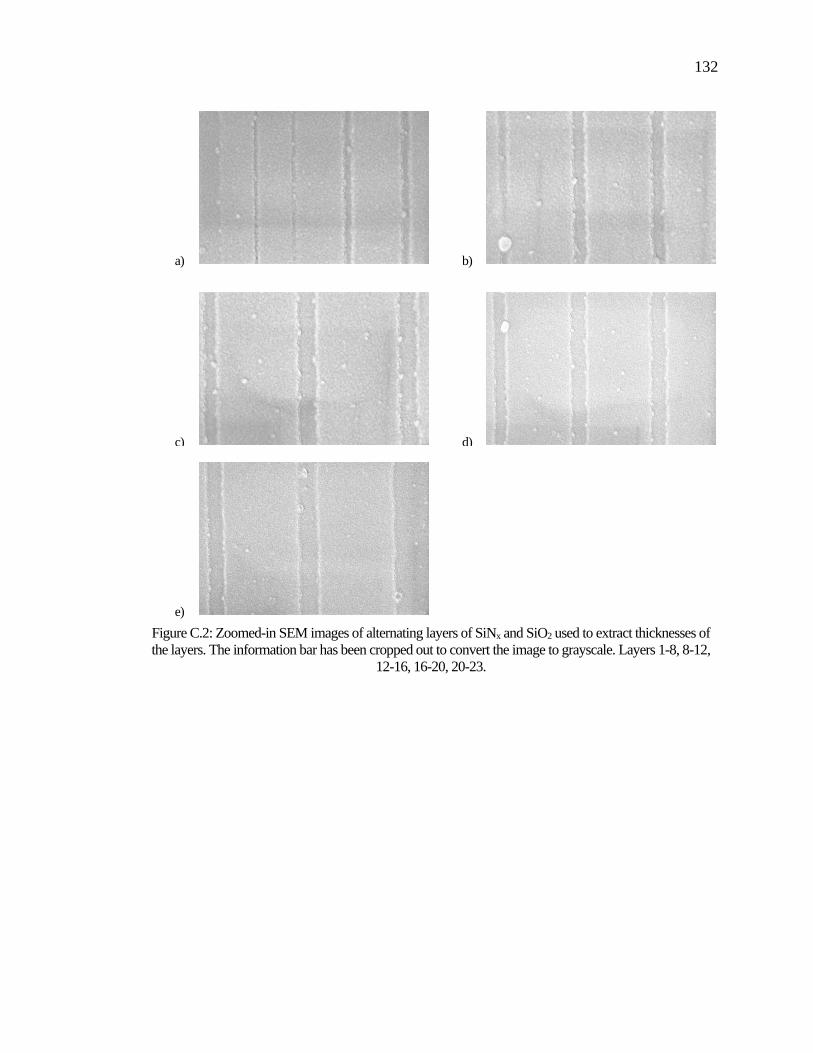
132
a) b)
c) d)
e)
Figure C.2: Zoomed-in SEM images of alternating layers of SiNx and SiO2 used to extract thicknesses of
the layers. The information bar has been cropped out to convert the image to grayscale. Layers 1-8, 8-12,
12-16, 16-20, 20-23.

133
Figure C.3: SEM image intensity summed top to bottom. Layers 1-6, 6-10, 10-14, 14-16, 16-20, 20-23
Calibration curves obtained from three such points around the fiber cross section
are given in Figure C.4 and values of thicknesses are tabulated in Table 11. The slopes of
these curves is about 26 nm/min differing only at the scale of Angstroms.
-200 0 200 400 600 800 1000 1200 1400-20
0
20
40
60
80
100
120
140
160
B
A
B
-200 0 200 400 600 800 1000120014001600
0
50
100
150
200
D
C
D
-200 0 200 400 600 800 1000120014001600-20
0
20
40
60
80
100
120
140
160
180
F
E
F
500 1000
0
70
140
H
G
H
0 500 1000 1500 2000 2500
0
50
100
150
200
250
J
I
J
0 500 1000 1500 2000 2500
0
20
40
60
80
100
120
L
K
L

134
10 15 20 25 30
200
300
400
500
600
700
800
Thic
kness 6
T (
nm
)
Deposition Time (min)
SiN
Linear Fit of Thickness 6T
Equation y = a + b*x
Weight Instrumental
Residual Sum of Squares
4.18432
Adj. R-Square
0.99791
Value Standard Error
Thickness 6T
Intercept -37.56851
8.06527
Slope 26.59403
0.5673
10 15 20 25 30100
200
300
400
500
600
700
800
Thic
kness (
nm
)
Deposition Time (min)
SiN
Linear Fit of Thickness
Equation y = a + b*x
Weight Instrumental
Residual Sum of Squares
6.13375
Adj. R-Square
0.99649
Value Standard Error
ThicknessIntercept -46.0064
710.13144
Slope 26.34737
0.60653

135
Figure C.4: Growth Rate curve from three points around the fiber cross section.
Matlab code for processing of SEM images clc;
I= imread('SEM_FileName.tif');
%If image when cropped becomes m X n X 4 instead of m X n X 3, then
include I=I(:,:,1:3)
im=rgb2gray(I);
%im=imrotate(im,0.5);
figure, imshow(im), title('original image');
im=imadjust(im);imshow(im)
% im=medfilt2(im,[3 3]);
% h = fspecial('average');
% im = imfilter(im,h);
% imshow(im), title('averaged');
im = wiener2(im,[12 12]);%wiener filter working good for 100kx images
% figure, imshow(im)
% im=im2bw(im,0.01);%could be very helping or very harmful..depends on
image.
% try removing or including it in the code to see the effect..and play
with
% param
% figure, imshow(im)
[junk threshold] = edge(im, 'sobel');
fudgeFactor = .5;
10 15 20 25 30
200
300
400
500
600
700
800
Th
ickn
ess 6
R
Deposition Time (min)
SiN
Linear Fit of Thickness 6R
Equation y = a + b*x
Weight Instrumental
Residual Sum of Squares
2.41922
Adj. R-Square 0.99937
Value Standard Error
Thickness 6RIntercept -34.00396 7.02494
Slope 26.10012 0.40486

136
BWs = edge(im,'sobel', threshold * fudgeFactor);
figure, imshow(BWs), title('binary gradient mask');
e=im2double(BWs);
e1=e(1,:);
for d=1:size(e,1)
e1=e1+e(d,:);
end
figure
subplot(2,1,1)
plot(e1)
data=[1:size(e,2) ; e1]';
xlim([0 size(e,2)]);
subplot(2,1,2)
imshow(e),title('edge detect');
axis normal
se90 = strel('line', 3, 90);
se0 = strel('line', 1, 0);
BWsdil = imdilate(BWs, [se90 se0]);
figure, imshow(BWsdil), title('dilated gradient mask');
e=im2double(BWsdil);
e1=e(1,:);
for d=1:size(e,1)
e1=e1+e(d,:);
end
figure
subplot(2,1,1)
plot(e1)
xlim([0 size(e,2)]);
subplot(2,1,2)
imshow(e),title('dilated');
axis normal
seD = strel('diamond',1);
BWfinal = imerode(BWsdil,seD);
BWfinal = imerode(BWfinal,seD);
e=im2double(BWfinal);
e1=e(1,:);
% Summing intensity
for d=1:size(e,1)
e1=e1+e(d,:);
end
figure
subplot(2,1,1)
plot(e1)
xlim([0 size(e,2)]);
subplot(2,1,2)
imshow(e),title('Eroded');
axis normal
figure, imshow(BWfinal), title('segmented image');

137
BWoutline = bwperim(BWfinal);
Segout = I;
Segout(BWoutline) = 255;
figure, imshow(Segout), title('outlined original image');
Table 11: Thicknesses obtained from SEM images of layers for the 3 points around the cross
section.
Time
(min)
Thickness1
(nm)
Error1
(nm)
Time
(min)
Thickness2
(nm)
Error2
(nm)
Time
(min)
Thickness3
(nm)
Error3
(nm)
10 225 5.5 10 228 4.5 10 204.5 8.1
10 232.5 6.5 10 234.2 6.1 10 228.9 8.8
14 324.1 7.6 14 323.4 6.9 14 318.4 12.5
14 337.8 15.9 14 335.8 12 14 323.9 19.3
18 438.3 15.8 18 440.3 12.3 14 328.9 9.5
18 437.2 11.8 18 444.2 13.2 18 429.1 13.6
22 541 12.1 18 444.6 12.3 18 448.4 30.7
22 545.3 17.7 22 548.8 14.1 18 426.1 18.8
26 645.7 17.2 22 558.7 16.7 22 541 31.1
26 639 18.5 26 655.5 18.9 22 539.3 13.2
26 639.3 26 30 759.2 25.8 26 631.7 11.7
30 745 24.9 30 761.1 29.5 26 643.6 31
30 751 25.2 30 737.1 24.7
30 747.3 12.7 30 755.4 32
30 754.9 14.2
SiO2
Time
(s)
Thickness
(nm)
Error
(nm)
10 16.8 6.8
10 17.5 5.9
20 46.4 9.7
20 42.2 16.8
20 46.1 16.1
30 76.2 14.0
30 83.5 9.8
30 82.5 12.0
40 113.4 12.4
40 118.7 10.1
40 119.4 19.3
40 124.9 23.6
50 156.9 27.8
50 154.8 25.4
50 149.1 15.7
50 148.4 18.9

138
50 154.2 12.2
60 189.4 14.6
60 191.6 26.2
360 1245 27.9
C.1.2 Multiple Fibers with Single Layer Deposition
One layer of silicon nitride with different deposition time was deposited on 4 fibers
and SEM was performed to obtain the deposition rate. SEM was taken at only one point
unlike for the multilayered fiber. The slope is in agreement with the multilayer fiber.
Table 12: Thickness obtained from SEM of 4 single layered fibers.
Fiber ID Deposition Time Thickness [nm] Error [nm]
ZN9 10:49 251 14
ZN11 29 704 5
ZN12 39:1 984 9
ZN13 112:48 2947 21
Figure C.5: Growth Rate curve obtained from single layers deposited on different fibers.
0 20 40 60 80 100 120
0
500
1000
1500
2000
2500
3000
Th
ickn
ess (
nm
)
Deposition Time (min)
Thickness
Linear Fit of Thickness
Equation y = a + b*x
Weight Instrumental
Residual Sum of Squares
22.91962
Adj. R-Square 0.99933
Value Standard Error
ThicknessIntercept -61.45934 4.37327
Slope 26.60322 0.1178

139
APPENDIX D SPEED DEPENDENT REFRACTIVE INDEX
D.1 Experiment and Results
Different growth kinetics observed for static (Figure 4.17) and dynamic deposition
method (rotation) on fibers called for an investigation of effect of rotation speed. Four
fibers were coated with silicon nitride for 21 minutes at different RPM’s. During test
rotation, the fiber rotates smooth and calm. But during deposition, as seen through the
chamber viewing port, the fiber vibrates erratically as if some extra electrostatic forces are
acting due to possible charging of the objects introduced in the otherwise relatively empty
chamber. Naturally vibrations amplify with speed. The optical images of the fabricated
fibers in Figure D.1 have a greenish-brown hue with ZN17 (30 rpm) more dominantly
green. As mentioned in Chapter 3, this difference could be due to the fact that color also
depends on the point along the axis of the fiber imaged.
The coated fibers were characterized by Mie scattering. The scattering patterns with
best-fit patterns obtained are given in Figure D.1 and characterization results in Table 13.
Note that the pattern of ZN16 is similar to ZN17 while that of ZN22 is similar to ZN23.
This is because ZN16 and ZN17 were made out of old spool of substandard SMF28 of
unknown origin while ZN22 and ZN23 out of high quality spool of SMF28e+ distributed
by Fiber Instrument Sales. Running the root search for refractive index, thickness and
diameter of the substrate fiber as in Chapter 4 gave the values in Table 13.
The refractive index (n) is increasing monotonically with speed (Figure D.2) while
thickness has an overall increasing trend with a probable outlier at 15 rpm which could be
due to axial non-uniformity of the thickness. The extent of axial non-uniformity should be
characterized by SEM to estimate the degree of thickness variation in the fiber samples.

140
Nevertheless, the increase in refractive index is certain and has not been reported elsewhere.
Note that n for 3 rpm is close to that of silicon nitride at 632.8 nm. That means rotation
speed is what is affecting the composition more than elevation of the sample.
ZN16
ZN22
ZN17
ZN23
Figure D.1: Experimental Data vs best-fit scattering pattern for fibers fabricated at different
rotation speed.
Table 13: Roots search result
Fiber ID Deposition
Time
[min]
Material RPM Root
n t
[nm]
d [µm]
ZN16 21 SiNx 3 1.95 435 124.83
ZN22 21 SiNx 15 2.19 315 124.92
ZN17 21 SiNx 30 2.49 502 124.99
ZN23 21 SiNx 42 2.59 510 124.69
150 155 160 165 170 175
0
1
150 155 160 165 170 175
0
1
150 155 160 165 170 175
0
1
150 155 160 165 170 175
0
1
3RPM Data
BestFit
15RPM Data
BestFit
No
rma
lize
d S
ca
tte
rin
g 30RPM Data
theoretical
Scattering Angle [deg]
42RPM Data
BestFit

141
Figure D.2: Refractive index of SiNx films as a function of RPM determined from scattering of the coated
fibers. Four fibers were coated at 3, 15, 30 and 42 RPM respectively.
D.2 Discussion
The dependence of film properties on rotation speed is not surprising as gradual
deposition of the amorphous material is a multistep process each happening at a rate
determined by deposition conditions. Figure D.3 lists the differences in the deposition
conditions for static, slow and fast rotating fiber.
Lower Height Higher Higher
Metal Ring – affects flow field Metal chuck Metal chuck
Temperature – Higher Lower Lower
Temperature – Constant Cycling Cycling faster
Reactant flux – Non-uniform around
the fiber
Uniform Uniform
Static Rotating calmly Rotating with vigorous occasional
vibration
Figure D.3: Comparison of deposition conditions for stationary, slow and fast rotating fiber.
0 10 20 30 40 50
1.9
2.0
2.1
2.2
2.3
2.4
2.5
2.6
2.7
Refr
active Index
RPM

142
Explanation of the apparent increase in RI in specific needs investigation as we
don’t have a conjecture as to why the density or Si-content increased with speed which are
two possible factor of increased RI. It has been acknowledged in literature that many of the
processes leading to film deposition in PECVD are not well understood [48]. Apart from
the normally occurring processes such as electron impact creating ionized species, their
transport to substrate, surface migration, chemical reactions and desorption, in this case a
substrate of small surface area – a fiber is hanging in the middle of the plasma cloud
supported by a metal chuck, unlike a wafer that is in contact with the base platen generally.
It is known that geometry and material of the objects present in the plasma affect the flow
field distribution and ion density which affect the film composition and thickness [50].
A factor affecting density is ion bombardment rate [48] which controls the
precursor mobility on the surface. Higher ion bombardment rate means denser film thus
higher index. Another factor is rooted in the nature of initial stages of growth of SiNx on
silica. SiNx/SiO2 interface is non-wettable leading to formation of ‘islands’ [49] as the ions
migrate on the surface to growth sites and react. These islands eventually coalesce with
continued deposition forming a solid continuous film while the unreacted volatile
components desorb out of the film. If there isn’t enough time and temperature for the ions
to migrate, the film composition and physical properties will differ with speed. Also, as the
fiber is cycling through the temperature gradient between the electrodes, rate of surface
migration is expected to depend on speed [51]. To understand the initial growth stages,
SEM of initial deposition would be helpful. As far as Si content is concerned, an XRD or
Micro-Raman or other techniques are required to get the film composition.