Residual and intentional n-type doping of ZnO thin films grown by metal-organic vapor phase epitaxy...
11
Residual and intentional n-type doping of ZnO thin films grown by metal-organic vapor phase epitaxy on sapphire and ZnO substrates Stéphane Brochen, Matthieu Lafossas, Ivan-Christophe Robin, Pierre Ferret, Frédérique Gemain, Julien Pernot, and Guy Feuillet Citation: Journal of Applied Physics 115, 113508 (2014); doi: 10.1063/1.4868591 View online: http://dx.doi.org/10.1063/1.4868591 View Table of Contents: http://scitation.aip.org/content/aip/journal/jap/115/11?ver=pdfcov Published by the AIP Publishing Articles you may be interested in Photoluminescence and secondary ion mass spectrometry investigation of unintentional doping in epitaxial germanium thin films grown on III-V compound by metal-organic chemical vapor deposition J. Appl. Phys. 111, 013502 (2012); 10.1063/1.3673538 High resolution photoluminescence spectroscopy of donors in undoped and In-doped ZnO grown by metalorganic vapor phase epitaxy J. Appl. Phys. 110, 083506 (2011); 10.1063/1.3652854 Influence of thermally diffused aluminum atoms from sapphire substrate on the properties of ZnO epilayers grown by metal-organic chemical vapor deposition J. Vac. Sci. Technol. A 29, 03A106 (2011); 10.1116/1.3549136 Microstructural compositional, and optical characterization of GaN grown by metal organic vapor phase epitaxy on ZnO epilayers J. Vac. Sci. Technol. B 27, 1655 (2009); 10.1116/1.3137967 Electrical and optical studies of metal organic chemical vapor deposition grown N-doped ZnO films J. Vac. Sci. Technol. B 27, 1705 (2009); 10.1116/1.3110018 [This article is copyrighted as indicated in the article. Reuse of AIP content is subject to the terms at: http://scitation.aip.org/termsconditions. Downloaded to ] IP: 132.168.108.11 On: Tue, 29 Apr 2014 16:06:24
-
Upload
independent -
Category
Documents
-
view
3 -
download
0
Transcript of Residual and intentional n-type doping of ZnO thin films grown by metal-organic vapor phase epitaxy...

Residual and intentional n-type doping of ZnO thin films grown by metal-organic vaporphase epitaxy on sapphire and ZnO substratesStéphane Brochen, Matthieu Lafossas, Ivan-Christophe Robin, Pierre Ferret, Frédérique Gemain, Julien Pernot,
and Guy Feuillet
Citation: Journal of Applied Physics 115, 113508 (2014); doi: 10.1063/1.4868591 View online: http://dx.doi.org/10.1063/1.4868591 View Table of Contents: http://scitation.aip.org/content/aip/journal/jap/115/11?ver=pdfcov Published by the AIP Publishing Articles you may be interested in Photoluminescence and secondary ion mass spectrometry investigation of unintentional doping in epitaxialgermanium thin films grown on III-V compound by metal-organic chemical vapor deposition J. Appl. Phys. 111, 013502 (2012); 10.1063/1.3673538 High resolution photoluminescence spectroscopy of donors in undoped and In-doped ZnO grown bymetalorganic vapor phase epitaxy J. Appl. Phys. 110, 083506 (2011); 10.1063/1.3652854 Influence of thermally diffused aluminum atoms from sapphire substrate on the properties of ZnO epilayersgrown by metal-organic chemical vapor deposition J. Vac. Sci. Technol. A 29, 03A106 (2011); 10.1116/1.3549136 Microstructural compositional, and optical characterization of GaN grown by metal organic vapor phase epitaxyon ZnO epilayers J. Vac. Sci. Technol. B 27, 1655 (2009); 10.1116/1.3137967 Electrical and optical studies of metal organic chemical vapor deposition grown N-doped ZnO films J. Vac. Sci. Technol. B 27, 1705 (2009); 10.1116/1.3110018
[This article is copyrighted as indicated in the article. Reuse of AIP content is subject to the terms at: http://scitation.aip.org/termsconditions. Downloaded to ] IP:
132.168.108.11 On: Tue, 29 Apr 2014 16:06:24
Residual and intentional n-type doping of ZnO thin films grown bymetal-organic vapor phase epitaxy on sapphire and ZnOsubstrates
St�ephane Brochen,1,2,3 Matthieu Lafossas,1 Ivan-Christophe Robin,1 Pierre Ferret,1
Fr�ed�erique Gemain,1 Julien Pernot,2,3,4 and Guy Feuillet11CEA-LETI, MINATEC Campus, 17 rue des Martyrs, F-38054 Grenoble Cedex 9, France2Univ. Grenoble Alpes, Inst. NEEL, F-38042 Grenoble, France3CNRS, Inst. NEEL, F-38042 Grenoble, France4Institut Universitaire de France, 103 boulevard Saint Michel, 75005 Paris, France
(Received 21 November 2013; accepted 4 March 2014; published online 20 March 2014)
ZnO epilayers usually exhibit high n-type residual doping which is one of the reasons behind the
difficulties to dope this material p-type. In this work, we aimed at determining the nature of the
involved impurities and their potential role as dopant in ZnO thin films grown by metalorganic
vapor phase epitaxy (MOVPE) on sapphire and ZnO substrates. In both cases, secondary ion mass
spectroscopy (SIMS) measurements give evidence for a strong diffusion of impurities from the
substrate to the epilayer, especially for silicon and aluminum. In the case of samples grown on
sapphire substrates, aluminum follows Fick’s diffusion law on a wide growth temperature range
(800� 1000 �C). Thus, the saturation solubility and the diffusion coefficient of aluminum in ZnO
single crystals have been determined. Furthermore, the comparison between SIMS impurity and
effective dopant concentrations determined by capacitance-voltage measurements highlights, on
one hand a substitutional mechanism for aluminum diffusion, and on the other hand that silicon
acts as a donor in ZnO and not as an amphoteric impurity. In addition, photoluminescence spectra
exhibit excitonic recombinations at the same energy for aluminum and silicon, indicating that
silicon behaves as an hydrogenic donor in ZnO. Based on these experimental observations, ZnO
thin films with a controlled n-type doping in the 1016 � 1019cm�3 range have been carried out.
These results show that MOVPE growth is fully compatible with the achievement of highly
Al-doped n-type thin films, but also with the growth of materials with low residual doping, which
is a crucial parameter to address ZnO p-type doping issues. VC 2014 AIP Publishing LLC.
[http://dx.doi.org/10.1063/1.4868591]
I. INTRODUCTION
ZnO is a widely studied II–VI semiconductor, especially
for optoelectronic applications like near ultraviolet light emit-
ters or detectors.1 Nevertheless, it is well known that the de-
velopment of an all ZnO optoelectronic device is hampered
by p-type doping difficulties.2,3 A good understanding of the
residual n-type doping appears as an important preliminary
step to try and understand the origin of these difficulties.
Metalorganic vapor phase epitaxy (MOVPE) is a widely
used method for the epitaxial growth of semiconductor thin
films, especially for large scale industrial opto-electronic
applications as light emitting diodes or laser diodes (e.g., for
nitride-related material devices). This vapor phase growth
method, which allows the achievement of ZnO thin films
with a high crystalline quality,4–8 is a relevant method for
doping studies because of a large choice of metalorganic pre-
cursors and a good control of film stoichiometry.
In this paper, we have investigated both residual and
intentional n-type doping, with aluminum impurities, of ZnO
thin films grown by MOVPE. For the sake of comparison, the
ZnO epilayers were grown on sapphire and ZnO substrates.
In this framework, we have combined capacitance-voltage
C(V) measurements and secondary ion mass spectroscopy
(SIMS) in order to investigate the role of some impurities on
the effective dopant concentration profiles. Correlatively,
photoluminescence measurements were also performed on
these samples to investigate the role of donor impurities on
the optical properties of ZnO thin films and especially on
excitonic recombinations in the ZnO near band edge region.
II. GROWTH AND EXPERIMENTAL DETAILS
The ZnO epilayers were grown by MOVPE in a 6 � 2
in. close coupled shower head Aixtron system using diethyl-
zinc (DEZn) and N2O as a source of zinc and oxygen,
respectively, and with N2 as carrier gas. The system is also
equipped with an O2 line used for annealing steps and also as
another source of oxygen for the low temperature growth re-
gime. In the case of intentionally n-doped samples, trimethyl
aluminum ðC6H18Al2Þ is used as source of aluminum. The
growth temperature is measured using an in-situ pyrometer
system at 633 nm (Laytec epicurveTT system).
The growth conditions are optimized with a VI/II molar
flow ratio of 6700 and with a reactor pressure between 50
and 200 millibars in the temperature range of 500� 1000 �C,
with several growth steps as described in Figure 1; at first
substrate annealing under O2 at 1070 �C during 300 s, then
nucleation layer growth under O2 and DEZn at 520 �C during
1840s (�450nm), followed by an annealing under O2 þ N2O
0021-8979/2014/115(11)/113508/10/$30.00 VC 2014 AIP Publishing LLC115, 113508-1
JOURNAL OF APPLIED PHYSICS 115, 113508 (2014)
[This article is copyrighted as indicated in the article. Reuse of AIP content is subject to the terms at: http://scitation.aip.org/termsconditions. Downloaded to ] IP:
132.168.108.11 On: Tue, 29 Apr 2014 16:06:24

at 965 �C during 300 s. The main growth regime under N2Oand DEZn begins at 935 �C during 1200 s (�150 nm) and
continues with a temperature and a duration noted Tg and tg,
respectively, in the following. The growth duration tg is set
in order to obtain typical thicknesses around a few lm at a
growth temperature Tg varying between 800 and 1000 �C.
The growth conditions for the different samples are given in
Table I (heteroepitaxial thin films), Table II (homoepitaxial
thin films), and Table III (intentionally aluminum doped thin
films).
The impurity concentration profiles were measured on
our sample series by SIMS both in the positive ion detection
mode with a Csþ primary ion bombardment accelerated at
14:5 keV and in the negative ion detection mode with a 02þ
primary ion bombardment accelerated at 5:5 keV (analyses
at Probion SA, France).
The effective dopant concentration profiles ND � NA are
measured by capacitance-voltage C(V) measurements using
a 720 lm diameter double Schottky mercury probe with a
20 Hz� 1 MHz Agilent LCR meter (4284 A) in parallel
mode. In the case of highly Al-doped samples, an oxygen
plasma treatment is performed in order to limit leakage cur-
rent in the Schottky diodes.9 After this treatment, a strong
increase of the rectifying behavior in the I(V) characteristics
is observed (not shown), allowing an accurate determination
of the effective dopant concentration profiles with respect to
the diode cutoff frequency, as described in Ref. 10
The PL spectra were obtained at 10 K by using a
frequency-doubled 244 nm cw Ar laser coupled with a
0:55 m monochromator equipped with a 1800 mm�1 grating.
The excitation conditions are the same for all samples.
III. RESULTS AND DISCUSSIONS
A. Identification of impurities
In a first step, the impurity concentration has been inves-
tigated by secondary ion mass spectroscopy (SIMS) in ZnO
thin films grown by MOVPE both on ZnO and sapphire sub-
strates. Typical SIMS concentration profiles of group III (B,
FIG. 1. MOVPE growth steps conditions: (1) Substrate surface annealing
under O2 at 1070 �C during 300 s; (2) Growth of the nucleation layer under
O2 and DEZn at 520 �C during 1840 s (�450 nm); (3) Annealing of the
nucleation layer under O2 þ N2O at 965 �C during 300 s; (4) Regrowth under
N2O and DEZn at 935 �C during 1200 s (�150 nm); and (5) Main growth re-
gime under N2O and DEZn at Tg and during tg.
TABLE I. Epilayer thickness, growth conditions (duration and temperature), aluminum diffusion parameters (diffusion coefficient DAl and saturation solubility
CsatAl ), and mean value of the effective dopant concentration ND � NA of undoped ZnO samples grown on sapphire substrates.
Sample Thickness (lm) Duration tg sð Þ Temperature Tgð �CÞ DAl ðcm2:s�1Þ CsatAl (cm�3) ND � NA (cm�3)
#1 3.3 13 050 800 7:9� 10�14 2:7� 1018 5:8� 1016
#2 3.4 13 050 860 4:5� 10�13 1:8� 1018 1:1� 1017
#3 2.0 6600 880 3:3� 10�13 2:2� 1018 5:8� 1016
#4 4.8 17 400 930 1:5� 10�12 2:6� 1018 2:1� 1017
#5 1.1 6000 990 7:2� 10�12 3:6� 1018 4:2� 1018
TABLE II. Epilayer thickness, growth conditions (duration and temperature), mean value of the effective dopant concentration ND � NA, and average SIMS
concentration of aluminum and silicon of undoped ZnO thin film (#6) grown on O-polar ZnO substrate (#7).
Sample Thickness lmð Þ Duration tg sð Þ Temperature Tgð �CÞ ND � NA ðcm�3Þ Al½ � ðcm�3Þ Si½ � cm�3ð Þ
#6 3.4 13 050 860 2:7� 1016 1:3� 1015 4:5� 1016
#7 500 … … 1:8� 1017 1:9� 1016 2:0� 1017
TABLE III. Kind of substrate, epilayer thickness, growth conditions (duration and temperature), mean value of the effective dopant concentration ND � NA,
and average SIMS concentration of aluminum of intentionally Al-doped ZnO samples.
Sample Substrate Thickness lmð Þ Duration tg sð Þ Temperature Tgð �CÞ ND � NA ðcm�3Þ Al½ � ðcm�3Þ
#8 Sapphire 4.8 17 000 990 4:9� 1018 8:8� 1018
#9 ZnO (O-face) 2.6 17 000 990 4:5� 1018 7:5� 1018
#10 ZnO (Zn-face) 2.3 17 000 990 2:3� 1018 6:3� 1018
113508-2 Brochen et al. J. Appl. Phys. 115, 113508 (2014)
[This article is copyrighted as indicated in the article. Reuse of AIP content is subject to the terms at: http://scitation.aip.org/termsconditions. Downloaded to ] IP:
132.168.108.11 On: Tue, 29 Apr 2014 16:06:24

Al, Ga, and In), I (H and Li) and IV (Si and C) impurities,
measured on such ZnO epilayers are plotted in Figure 2.
These impurities have been selected because they are sup-
posed to have an important role on the electrical properties
of ZnO samples. For the sake of comparison, the two ZnO
samples in Figure 2 have been grown in the same run, at
a growth temperature Tg ¼ 860 �C and a growth duration tg
¼ 13050 s corresponding to a layer thickness around 3:4 lm.
As shown in Figures 2(a) and 2(b), the concentrations of
hydrogen (H) and carbon (C) impurities appear to be rela-
tively high (>1:0� 1018cm�3) for the two samples analysed
here, both in the layer and the substrate. This could indicate
that the concentration of hydrogen and carbon may originate
from the SIMS measuring chamber and not necessarily from
the ZnO samples analyzed here. Indeed, even if hydrogen is
regarded as a cause of doping in ZnO,11,12 and carbon as an
amphoteric but electrically active impurity in ZnO,13,14 it is
difficult to determine the exact concentration of these ele-
ments in our samples, because they are abundant and diffi-
cult to remove totally from the SIMS chamber, leading to a
high detection limit in the sample.
Inversely, boron (B), indium (In), and gallium (Ga) con-
centrations are relatively low (<5:0� 1015cm�3) and close
to the SIMS detection threshold for both samples. Despite
their significant potential role on the n-type conductivity in
ZnO,15,16 these species are suspected to have a negligible
influence on the electrical properties of the ZnO epilayers
due to their relatively low concentrations.
In the case of the homo-epitaxial sample, the Figure 2(a)
reveals relatively low aluminum (Al) and lithium (Li) con-
centrations in the ZnO epilayer, lower than 5:0� 1015 and
5:0� 1016cm�3, respectively, which slightly diffuse from
the ZnO substrate into the ZnO epilayer. Similarly, the SIMS
silicon (Si) profile provides also evidence that silicon has
also diffused into the epilayer but with a maximum silicon
concentration at the substrate-layer interface larger than
3:0� 1018cm�3. Like carbon, silicon in ZnO is considered
as an amphoteric dopant which could act as a donor if on a
zinc site SiZn or as an acceptor if on an oxygen site SiO.17–19
In the case of the hetero-epitaxial samples grown on sap-
phire, the SIMS profiles shown in Figure 2(b) reveal an
extremely low lithium (Li) concentration, close to the SIMS
detection threshold both in the substrate and in the epitaxial
ZnO layer. On contrary, aluminum (Al) and silicon (Si) SIMS
profiles indicate a strong diffusion of these impurities within
the ZnO thin film, as in the previous homo-epitaxial case, with
concentrations larger than 1:0� 1018cm�3 at the sapphire-ZnO
interface for these two species. Nevertheless, the diffusion pro-
file is less extended for hetero-, than for homo-epitaxial sam-
ples and seems to originate exclusively from the substrate-layer
interface with a silicon concentration around 3:5� 1018cm�3
at the interface for this particular sample. This silicon contami-
nation may result from exposure of the substrate surface to air
and/or from chemo-mechanical polishing residues.
Unfortunately, even if silicon SIMS measurements show
typical diffusion profiles, the silicon concentration at the sub-
strate surface is intrinsically uncontrolled and did not allow
us to perform relevant quantitative analysis of these diffusion
profiles, such as the one we will implement below in the case
of aluminum.
In the case of aluminum, the SIMS concentration profile
plotted in Figure 2(b) also exhibits a typical diffusion profile
spreading over a few micrometers. Moreover, aluminum
impurities appear to come from the sapphire substrate as al-
ready observed by Tang et al.20 also in the case of ZnO thin
films grown by MOVPE on sapphire substrates. In this case,
as we will see in the following, the aluminum concentration
at the Al2O3=ZnO interface results from thermodynamic
equilibrium during MOVPE growth between the zinc oxide
thin film and an infinite reservoir of aluminum, consisting of
the sapphire substrate itself. Using Fick’s diffusion law, this
allows to determine the diffusion coefficient and the satura-
tion solubility of aluminum in ZnO.
B. Aluminum diffusion
In order to further investigate aluminum diffusion in
ZnO during MOVPE growth, the influence of the growth
FIG. 2. Typical SIMS impurity profiles, performed on ZnO layers grown by MOVPE, at the same growth temperature (860 �C), on ZnO (a) and sapphire (b)
substrates.
113508-3 Brochen et al. J. Appl. Phys. 115, 113508 (2014)
[This article is copyrighted as indicated in the article. Reuse of AIP content is subject to the terms at: http://scitation.aip.org/termsconditions. Downloaded to ] IP:
132.168.108.11 On: Tue, 29 Apr 2014 16:06:24
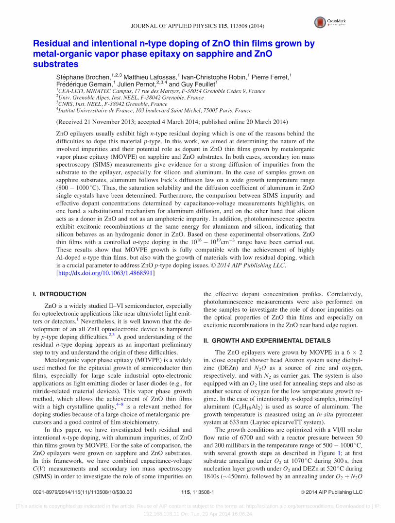
temperature has been studied in the case of thin films grown
on sapphire substrates. Figure 3 shows the aluminum concen-
tration profiles determined by SIMS on samples #1 to #5,
listed in Table I, for growth temperatures from 800 �C to
990 �C and a growth duration between 6000 s and 17400 s cor-
responding to layers thicknesses of a few micrometers. The
SIMS aluminum profiles, in the 1� 1015 � 1� 1018cm�3
concentration range, confirm that aluminum diffused from the
sapphire substrate into the ZnO epilayer for all samples.
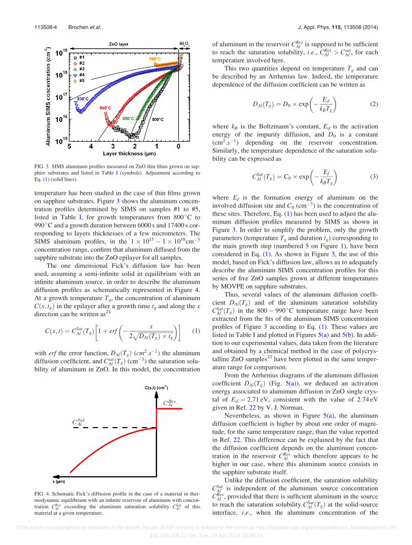
The one dimensional Fick’s diffusion law has been
used, assuming a semi-infinite solid in equilibrium with an
infinite aluminum source, in order to describe the aluminum
diffusion profiles as schematically represented in Figure 4.
At a growth temperature Tg, the concentration of aluminum
Cðx; tgÞ in the epilayer after a growth time tg and along the xdirection can be written as21
C x; tð Þ ¼ CSatAl Tgð Þ 1þ erf � x
2ffiffiffiffiffiffiffiffiffiffiffiffiffiffiffiffiffiffiffiffiffiffiffiffiffiDAl Tgð Þ � tg
p� �� �(1)
with erf the error function, DAlðTgÞ (cm2:s�1) the aluminum
diffusion coefficient, and CsatAl ðTgÞ (cm�3) the saturation solu-
bility of aluminum in ZnO. In this model, the concentration
of aluminum in the reservoir CResAl is supposed to be sufficient
to reach the saturation solubility, i.e., CResAl > Csat
Al , for each
temperature involved here.
This two quantities depend on temperature Tg and can
be described by an Arrhenius law. Indeed, the temperature
dependence of the diffusion coefficient can be written as
DAl Tgð Þ ¼ D0 � exp � Ed
kBTg
� �(2)
where kB is the Boltzmann’s constant, Ed is the activation
energy of the impurity diffusion, and D0 is a constant
(cm2:s�1) depending on the reservoir concentration.
Similarly, the temperature dependence of the saturation solu-
bility can be expressed as
CSatAl Tgð Þ ¼ C0 � exp � Ef
kBTg
� �(3)
where Ef is the formation energy of aluminum on the
involved diffusion site and C0 (cm�3) is the concentration of
these sites. Therefore, Eq. (1) has been used to adjust the alu-
minum diffusion profiles measured by SIMS as shown in
Figure 3. In order to simplify the problem, only the growth
parameters (temperature Tg and duration tg) corresponding to
the main growth step (numbered 5 on Figure 1), have been
considered in Eq. (1). As shown in Figure 3, the use of this
model, based on Fick’s diffusion law, allows us to adequately
describe the aluminum SIMS concentration profiles for this
series of five ZnO samples grown at different temperatures
by MOVPE on sapphire substrates.
Thus, several values of the aluminum diffusion coeffi-
cient DAlðTgÞ and of the aluminum saturation solubility
CSatAl ðTgÞ in the 800� 990 �C temperature range have been
extracted from the fits of the aluminum SIMS concentration
profiles of Figure 3 according to Eq. (1). These values are
listed in Table I and plotted in Figures 5(a) and 5(b). In addi-
tion to our experimental values, data taken from the literature
and obtained by a chemical method in the case of polycrys-
talline ZnO samples22 have been plotted in the same temper-
ature range for comparison.
From the Arrhenius diagrams of the aluminum diffusion
coefficient DAlðTgÞ (Fig. 5(a)), we deduced an activation
energy associated to aluminum diffusion in ZnO single crys-
tal of Ed ¼ 2:71 eV, consistent with the value of 2:74 eV
given in Ref. 22 by V. J. Norman.
Nevertheless, as shown in Figure 5(a), the aluminum
diffusion coefficient is higher by about one order of magni-
tude, for the same temperature range, than the value reported
in Ref. 22. This difference can be explained by the fact that
the diffusion coefficient depends on the aluminum concen-
tration in the reservoir CResAl which therefore appears to be
higher in our case, where this aluminum source consists in
the sapphire substrate itself.
Unlike the diffusion coefficient, the saturation solubility
CSatAl is independent of the aluminum source concentration
CResAl , provided that there is sufficient aluminum in the source
to reach the saturation solubility CSatAl ðTgÞ at the solid-source
interface, i.e., when the aluminum concentration of the
FIG. 3. SIMS aluminum profiles measured on ZnO thin films grown on sap-
phire substrates and listed in Table I (symbols). Adjustment according to
Eq. (1) (solid lines).
FIG. 4. Schematic Fick’s diffusion profile in the case of a material in ther-
modynamic equilibrium with an infinite reservoir of aluminum with concen-
tration CResAl exceeding the aluminum saturation solubility CSat
Al of this
material at a given temperature.
113508-4 Brochen et al. J. Appl. Phys. 115, 113508 (2014)
[This article is copyrighted as indicated in the article. Reuse of AIP content is subject to the terms at: http://scitation.aip.org/termsconditions. Downloaded to ] IP:
132.168.108.11 On: Tue, 29 Apr 2014 16:06:24
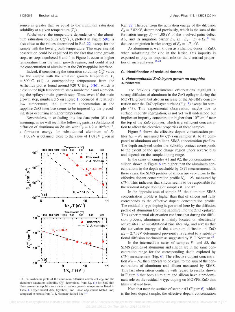
source is greater than or equal to the aluminum saturation
solubility at a given temperature (Tg).
Furthermore, the temperature dependence of the alumi-
num saturation solubility CSatAl ðTgÞ, plotted in Figure 5(b), is
also close to the values determined in Ref. 22, except for the
sample with the lower growth temperature. This experimental
observation could be explained by the fact that some growth
steps, as steps numbered 3 and 4 in Figure 1, occur at higher
temperature than the main growth regime, and could affect
the concentration of aluminum at the ZnO/sapphire interface.
Indeed, if considering the saturation solubility CSatAl value
for the sample with the smallest growth temperature Tg
¼ 800 �C (#1), a corresponding temperature from the
Arrhenius plot is found around 920 �C (Fig. 5(b)), which is
close to the high temperature steps numbered 3 and 4 preced-
ing the epilayer main growth step. Thus, even if the main
growth step, numbered 5 on Figure 1, occurred at relatively
low temperature, the aluminum concentration at the
sapphire-ZnO interface seems to be imposed by the preced-
ing steps occurring at higher temperature.
Nevertheless, in excluding this last data point (#1) and
assuming, as we will see in the following parts, a substitutional
diffusion of aluminum on Zn site with C0 ¼ 4:2� 1022cm�3,
a formation energy for substitutional aluminum of Ef
¼ 1:00 eV is obtained, close to the value of 1:08 eV given in
Ref. 22. Thereby, from the activation energy of the diffusion
Ed ¼ 2:82 eV, determined previously, which is the sum of the
formation energy Ef ¼ 1:00 eV of the involved point defect
AlZn and its migration barrier Eb, i.e., Ed ¼ Ef þ Eb,23 we
deduce a migration barrier energy of Eb ¼ 1:71 eV.
As aluminum is well known as a shallow donor in ZnO,
when substituting for zinc in the lattice, this impurity is
expected to play an important role on the electrical proper-
ties of such epilayers.16,24
C. Identification of residual donors
1. Heteroepitaxial ZnO layers grown on sapphiresubstrates
The previous experimental observations highlight a
strong diffusion of aluminum in the ZnO epilayer during the
MOVPE growth but also an increase of the Al-SIMS concen-
tration near the ZnO epilayer surface (Fig. 3) except for sam-
ple (#3). This experimental observation, maybe due to
surface impurity segregation, is not yet well understood but
implies an impurity concentration higher than 1016cm�3 near
the top of the ZnO epilayer, which is a sufficient concentra-
tion to affect the electrical properties of these samples.
Figure 6 shows the effective dopant concentration pro-
files ND � NA measured by C(V) on samples #1 to #5 com-
pared to aluminum and silicon SIMS concentration profiles.
The depth analyzed under the Schottky contact corresponds
to the extent of the space charge region under reverse bias
and depends on the sample doping range.
In the cases of samples #1 and #2, the concentrations of
silicon shown in Figure 6 are higher than the aluminum con-
centrations in the depth reachable by C(V) measurements. In
these cases, the SIMS profiles of silicon are very close to the
effective dopant concentration profile ND � NA measured by
C(V). This indicates that silicon seems to be responsible for
the residual n-type doping of samples #1 and #2.
In the opposite case of sample #3, the aluminum SIMS
concentration profile is higher than that of silicon and fully
corresponds to the effective dopant concentration profile.
The residual n-type doping is governed here by the diffusion
profile of aluminum from the sapphire into the ZnO epilayer.
This experimental observation confirms that during the diffu-
sion process, aluminum is mainly located on electrically
active sites like substitutional zinc sites AlZn and reveals that
the activation energy of the aluminum diffusion in ZnO
Ed ¼ 2:71 eV determined previously is related to a substitu-
tional diffusion mechanism as suggested by V. J. Norman.22
In the intermediate cases of samples #4 and #5, the
SIMS profiles of aluminum and silicon are in the same con-
centration range for the corresponding depth explored by
C(V) measurement (Fig. 6). The effective dopant concentra-
tion ND � NA then appears to be equal to the sum of the con-
centrations of aluminum and silicon measured by SIMS.
This last observation confirms with regard to results shown
in Figure 6 that both aluminum and silicon have a predomi-
nant role on the residual n-type doping on MOVPE ZnO thin
films analysed here.
Note that near the surface of sample #3 (Figure 6), which
is the less doped sample, the effective dopant concentration
FIG. 5. Arrhenius plots of the aluminum diffusion coefficient DAl and the
aluminum saturation solubility CSatAl determined from Eq. (1) for ZnO thin
films grown on sapphire substrates at various growth temperatures listed in
Table I. Experimental data (symbols) and linear adjustment (doted line)
compared to results from V. J. Norman (dashed line).22
113508-5 Brochen et al. J. Appl. Phys. 115, 113508 (2014)
[This article is copyrighted as indicated in the article. Reuse of AIP content is subject to the terms at: http://scitation.aip.org/termsconditions. Downloaded to ] IP:
132.168.108.11 On: Tue, 29 Apr 2014 16:06:24

profile ND � NA decreases more rapidly than the aluminum
diffusion profile, reaching a doping concentration ND � NA
< ½Al� þ ½Si�. This experimental observation could be
explained by donor compensation by an acceptor concentra-
tion NA around 2:0� 1016cm�3 and seems to indicate the ab-
sence of another donor level in this concentration range.
2. Homoepitaxial ZnO layers
In order to try and minimize impurity diffusion from the
ZnO substrate to the epilayer, a homoepitaxial ZnO thin film
has been grown at relatively low temperature (860 �C) with a
relatively large thickness (�3:5 lm), as reported in Table II.
The homoepitaxial thin film (sample #6) has been grown in a
single step on an O-polar hydrothermal ZnO single crystal
substrate (from Tokyo Denpa).
Similarly to ZnO layers grown on sapphire substrates,
SIMS concentration profiles of aluminum and silicon measured
on ZnO homoepitaxial layer (sample #6) have been compared
to the effective dopant concentration profiles (Fig. 7). In order
to compare residual n-type doping of the ZnO epilayer to the
bulk ZnO substrate, SIMS and C(V) have equally been per-
formed on the rear surface of the ZnO substrate (sample #7).
The SIMS concentration profiles of silicon are in both
cases, ZnO epilayer and substrate, higher than the aluminum
profiles and close to the effective dopant concentration pro-
files measured by C(V) as shown on the Figure 7. This obser-
vation is consistent with the results obtained in Sec. III C 1,
about heteroepitaxial ZnO thin films grown on sapphire sub-
strates, and confirms that silicon impurity acts as a donor dop-
ant in ZnO and can be responsible, at sufficient concentration,
for the residual n-type doping of ZnO samples.
Note that the donor behavior of silicon in ZnO is con-
sistent with density functional theory analysis which predicts
that Si preferentially substitute Zn in ZnO, acting as a
FIG. 6. Aluminum (circles) and silicon (stars) SIMS concentration profiles
compared to C(V) effective dopant concentration profiles ND � NA (squares)
measured on undoped ZnO thin films grown on sapphire substrates and listed in
Table I. The Schottky contact is located at the origin of the x-axis (zero depth).
FIG. 7. Aluminum (circles) and silicon (stars) SIMS concentration profiles
and C(V) effective dopant concentration profiles ND � NA (squares) measured
on undoped ZnO thin films (#6) grown on ZnO substrates (#7) and listed in
Table II. The Schottky contact is located at the origin of the x-axis (zero depth).
113508-6 Brochen et al. J. Appl. Phys. 115, 113508 (2014)
[This article is copyrighted as indicated in the article. Reuse of AIP content is subject to the terms at: http://scitation.aip.org/termsconditions. Downloaded to ] IP:
132.168.108.11 On: Tue, 29 Apr 2014 16:06:24

shallow donor.17–19 However, the most favourable associated
Si impurity form is expected to be the double donor Si2þZn
charge state. This appears to be in contradiction both with
our observations and with other experimental works involv-
ing an effective single donor behaviour of silicon in
ZnO,25–27 which may be due to a more complex form of Si-
related shallow donor levels in ZnO.
Moreover, from C(V) measurements the residual n-type
doping is about one order of magnitude less in the ZnO epi-
layer than in the ZnO hydrothermal substrate with effective
dopant concentrations about ND � NA ¼ 2:7� 1016cm�3 and
ND � NA ¼ 1:8� 1017cm�3, respectively.
Notice furthermore that the concentration of acceptor lev-
els can be estimated, in considering aluminum and silicon as
majority donors, by NA ¼ ½Al� þ ½Si� � ðND � NAÞ ¼ 1:9�1016cm�3 which is close to the previously estimated value,
of about 2:0� 1016cm�3, in the case of heteroepitaxial ZnO
thin films grown on sapphire substrates (sample #3). This
acceptor concentration NA includes all the acceptor levels
located below the Fermi level, associated for example to the
presence of intrinsic acceptor defects,23 and appears to be
lower in both homo- and hetero-epitaxial layers, than the value
estimated in a previous work on hydrothermal samples.28
Nevertheless, the same estimation in the case of the ZnO
substrate (#7) leads to an acceptor density NA ¼ 3:9�1016cm�3 which is certainly underestimated, due to the
presence of an additional donor level not linked to aluminum
and silicon impurities. Indeed, as already discussed in Ref. 28,
the coexistence of a deep and a shallow donor level with con-
centrations in the same order of magnitude as the compensa-
tion leads to a more realistic value of the acceptor density NA
in hydrothermal samples, higher than 1� 1017cm�3.
Moreover, this low compensation value in MOVPE epi-
layers is also consistent with transport measurements using
f-MEMSA analysis performed on a MOVPE homo-epitaxial
thin film, indicating a high carrier mobility channel in the
epilayer associated to a lower acceptor concentration NA in
the epilayer than in the ZnO substrate.29
D. Intentional n-type doping with aluminum
Having determined above that aluminum impurities dif-
fusing from the sapphire substrate could be responsible for
the residual n-type doping of the ZnO epilayers, we now turn
to aluminum intentional in-situ doping during the MOVPE
growth with trimethyl-aluminum ðC6H18Al2Þ used as source
of Al-dopant.
Moreover, in order to investigate the influence of the
substrate on aluminum incorporation during growth, three
ZnO thin films have been grown in the same run using three
different substrates as listed in Table III. Sample #8 has been
grown on a c-plane sapphire substrate while samples #9 and
#10 have been grown on O-polar and Zn-polar ZnO sub-
strates, respectively.
According to the results discussed previously about the
temperature dependence of the saturation solubility CSatAl (Fig.
5(b)), the n-doped ZnO thin films have been grown during
tg ¼ 17000 s at a growth temperature Tg ¼ 990 �C, as listed
in Table III, which corresponds to a concentration of alumi-
num in substitutional site estimated around 5:0� 1018cm�3.
After a preliminary study consisting in calibrating the alu-
minum incorporation by SIMS measurements as a function of
aluminum precursor flow (not shown), intentionally n-doped
ZnO thin films have been grown with a targeted aluminum
concentration around 5:0� 1018cm�3, according to the alumi-
num saturation solubility set by the growth temperature.
Figure 8 shows both the average aluminum SIMS con-
centrations (solid line) and the effective dopant concentra-
tion profiles (symbols) measured on the three intentionally
n-doped ZnO thin films (samples #8 to #10). In the three
cases, the aluminum SIMS concentration profiles reveal a
flat aluminum incorporation during the growth in the whole
epilayer thickness (not shown), but with a slight difference
of concentration as a function of the substrate used, as
reported in Table III.
The aluminum incorporation in the ZnO thin films, plot-
ted in Figure 8 and reported in Table III, appears to be higher
FIG. 8. Average aluminum SIMS con-
centration (solid lines), effective dop-
ant concentration profiles ND � NA
(symbols), and aluminum saturation
solubility (dashed lines) at a growth
temperature Tg ¼ 990 �C for intention-
ally in-situ Al doped ZnO thin films
grown by MOVPE on c-plane Al2O3
substrate (#8), on O-polar ZnO sub-
strate (#9), and on Zn-polar ZnO sub-
strate (#10) as listed in Table III. The
Schottky contact is located at the ori-
gin of the x-axis (zero depth).
113508-7 Brochen et al. J. Appl. Phys. 115, 113508 (2014)
[This article is copyrighted as indicated in the article. Reuse of AIP content is subject to the terms at: http://scitation.aip.org/termsconditions. Downloaded to ] IP:
132.168.108.11 On: Tue, 29 Apr 2014 16:06:24

in the case of sapphire substrates (sample #8) and is slightly
lower in the case of Zn-polar ZnO substrate (sample #10)
than for the oxygen polarity (sample #9), but stays in the
same doping range, a little higher than the targeted alumi-
num concentration.
Furthermore, the effective dopant concentration profiles
measured by C(V) and also plotted in Figure 8 confirm the
influence of the substrate on the doping efficiency. ZnO thin
films grown on sapphire and O-plane ZnO substrates (sam-
ples #8 and #9) exhibit an equivalent effective dopant con-
centration around 5:0� 1018 cm�3 as reported in Table III.
Sample #10 grown on Zn-polar ZnO substrate presents an
effective dopant concentration significantly smaller, around
2:0� 1018cm�3, indicating a poorer activation of aluminum
as a donor center in case of zinc polarity ZnO substrate.
These comparisons of the aluminum SIMS concentra-
tion ½Al� with the effective dopant concentrations ND � NA
lead to a doping efficiency ðND � NAÞ=½Al� about 56%, 60%,
and 37% for samples #8, #9, and #10, respectively. It is im-
portant to note here that these very high effective dopant
concentrations (ND � NA > 1� 1018cm�3) have been suc-
cessfully measured by C(V) thanks to the use of preliminary
oxygen plasma surface treatments, inducing an increase of
the rectifying behaviour of the Schottky diode.9
Taking into account the results obtained in the previous
section about aluminum diffusion from sapphire, the satura-
tion solubility of substitutional aluminum in ZnO CSatAl ðTgÞ
has also been reported in Figure 8 for a growth temperature
Tg ¼ 990 �C identical for all three samples. As shown in
Figure 8, the effective dopant concentrations in samples #8
and #9 are very close to the aluminum saturation solubility
CSatAl ð990 �CÞ unlike sample #10 in which the effective dopant
concentration is approximately twice lower.
For a SIMS aluminum concentration around 9:0�1018cm�3, as in sample #8 grown on sapphire substrate,
the temperature dependence of the substitutional aluminum
saturation solubility CSatAl ðTgÞ (Fig. 5(b)) indicates that in
order to increase the doping efficiency, the growth tempera-
ture should be higher than in this experiment, i.e., around
1070 �C rather than 990 �C. Indeed, the effective aluminum
concentration will not exceed the substitutional aluminum
concentration dictated by the growth temperature Tg.
Otherwise, beyond the saturation solubility, the excess alu-
minum atoms are not incorporated into the ZnO lattice on
zinc sites and seems to form electrically inactive centres30,31
which can furthermore induce crystal disorder.
E. Optical properties
Beyond the comparison that we carried out previously
between the concentration of aluminum and silicon impur-
ities, as determined from SIMS measurements, and the effec-
tive dopant concentration profiles ND � NA, as determined
from C(V) measurements, we undertook a comparison of the
optical and electrical properties of the different samples. For
this purpose, photoluminescence (PL) measurements have
been performed on samples with an effective donor concen-
trations ND � NA in the 1016 � 1019cm�3 doping range.
The PL spectra obtained from ZnO thin films with
increasing doping concentration are plotted in Figure 9, in
the 3.10–3:45 eV near band edge region. The spectra were
obtained with the same excitation conditions of 3Wcm�2 at a
temperature of 10 K and without normalization so that the
PL intensities of the different emissions can directly be com-
pared. In this energy range, the PL spectra are dominated by
excitonic recombinations, with free excitons (FX) or excitons
bound to neutral donors (D0X),32 followed by longitudinal
optical (LO) phonon replica with an energy separation of
72 meV.33
For all samples, the donor bound A-exciton D0XA emit-
ting at 3.361 eV, and assigned to the presence of an hydro-
genic donor as aluminum (I6)33 dominates the near band edge
emission but with intensities and widths varying with the do-
nor concentration. Note that whatever the respective concen-
tration of silicon and aluminum, the donor bound A-exciton
emission D0XA is at the same energy, indicating that both alu-
minum and silicon behave as hydrogenic donors.
Furthermore, the A-free exciton (FXA) emission at
3:375 eV is seen only for the homoepitaxial sample #6 with
FIG. 9. Photoluminescence measurements performed at 10 K on ZnO thin
films grown by MOVPE on both sapphire and ZnO substrates and containing
an increasing amount of effective dopant concentration ND � NA determined
by CðV) measurements as listed in Tables I–III. Dashed and doted lines indi-
cate the position of excitonic recombinations as described in the text.
113508-8 Brochen et al. J. Appl. Phys. 115, 113508 (2014)
[This article is copyrighted as indicated in the article. Reuse of AIP content is subject to the terms at: http://scitation.aip.org/termsconditions. Downloaded to ] IP:
132.168.108.11 On: Tue, 29 Apr 2014 16:06:24

the lowest residual doping level of 2� 1016cm�3. For this
sample, the LO phonon replica of the A-free exciton are also
clearly seen as well as the emission from the excited state of
the A-free exciton (n¼ 2) at 3:42 eV. For the other samples
with a higher donor concentration, the optical signatures of
the free exciton are no longer seen. Only the LO phonon rep-
lica of the A-free exciton (FXA � LO) are still seen for sam-
ples #1, #2, and #4 which have a donor concentration lower
than 2:0� 1017cm�3.
For the less doped samples (#6, #1, #2, and #4), with a
donor concentration lower than 2:0� 1017cm�3, the D0XA
and the D0XB emissions can be distinguished whereas this is
not the case for samples #10, #9, and #8 with a donor con-
centration higher than 2:0� 1018cm�3. For those samples
the only optical signatures seen are the D0XA emission and
its LO phonon replica.
Moreover, the full width at half maximum (FWHM) of
the D0XA photoluminescence emission (determined assum-
ing Gaussian distributions as illustrated by the dashed-doted
lines in Figure 9) on each samples analysed here and
reported in Figure 10 increases with the effective dopant
concentration measured by C(V). This bandwidth broadening
DE can be expressed as,34,35
DE ¼ DE0 þ DEI�B (4)
where DE0 is a constant associated in part to the intrinsic
linewidth at T¼ 0 and the thermal broadening at 10 K, and
DEI�B is the widening of the D0XA emission due to the impu-
rity band broadening DED with the increase of the dopant
concentration ND as36
DED �q2
e
4peNDð Þ
13 (5)
where qe is the electronic charge and e ¼ 7:8e0 is the static
dielectric constant in ZnO.33 Applying Haynes’ rule which
correlates the neutral donor-bound exciton DD0XA emission
energy with the donor ionization energy ED as DD0XA
¼ aDED, we can roughly estimate
DEI�B � aq2
e
4peNDð Þ
13: (6)
From experimental data adjustment (Fig. 9) and neglecting
the concentration of acceptors as ND � NA � ND, values of
DE0 ¼ 2:8 meV (at 10 K) and of a ¼ 0:2 are obtained. This
values of a ¼ 0:2 is consistent with Haynes’s constant values
a ¼ 0:2� 0:3 in ZnO.1 As shown in Figure 10, this simple
description allows to describe adequately the evolution of the
D0XA FWHM in this 3� 1016 � 5� 1018cm�3 doping range.
Note furthermore that for the intentionally Al-doped
samples #8, #9, and #10, the FWHM of the D0XA emission
has to be interpreted carefully because of an effective donors
concentration around 5� 1018cm�3, close to the expected
ZnO metal-insulator transition, and beyond which screening
by free electrons could affects directly the excitonic recom-
bination energy.37
Moreover, complementary X-ray diffraction measure-
ments (not shown) exclude the possible contribution of an in-
homogeneous strain on the increase of the D0XA FWHM
with the dopant concentration.
Moreover, since the donor concentration ND reported in
Figure 10 represents both the concentration of aluminum and
silicon, as demonstrated previously from the comparison of
C(V) and SIMS measurement, the broadening of the D0XA
photoluminescence bandwidth also suggests that Si behaves
like a donor in ZnO. Indeed, in the case of samples #1, #2,
and #6, where silicon is the major impurity, the D0XA recom-
bination occurs at the same energy than the one expected for
aluminum at 3:361 eV and labelled I6 in the literature.1,33
Nonetheless, this assumption would deserve to be confirmed
by other experiments, as the study of ZnO samples intention-
ally doped with silicon.
These optical results are in good agreement with what
was observed for non intentionally doped homoepitaxially
grown ZnO layers38 and confirm the doping evolution found
by C(V) and SIMS measurements as previously described.
IV. CONCLUSION
In the present study, the identification and the role of
some impurities on the electrical and optical properties of
ZnO thin films grown by metalorganic vapor phase epitaxy
(MOVPE) on both sapphire and ZnO substrates have been
investigated by employing complementary characterization
techniques, such as secondary ion mass spectroscopy
(SIMS), capacitance-voltage characteristics C(V), and photo-
luminescence (PL).
In a first step, SIMS analyses have revealed a strong im-
purity diffusion from the substrate to the epilayer during the
MOVPE growth. In the homo-epitaxial case, impurities
involved in these diffusion processes originate from residual
ZnO bulk impurities, such as lithium, aluminum, and silicon,
in addition to silicon surface contaminations. In the hetero-
epitaxial case, impurity diffusion concerns silicon, essen-
tially from surface contamination, and aluminum from the
sapphire substrate itself, resulting in typical diffusion profiles
spreading over a few micrometers.
Applying Fick’s diffusion law in the particular case of
samples grown on sapphire substrates to describe the
FIG. 10. Experimental (symbols) and simulated (solid line) photolumines-
cence bandwidth of the D0XA recombination at 10 K, according to Eq. (4)
with DE0 ¼ 2:75 meV (dashed line).
113508-9 Brochen et al. J. Appl. Phys. 115, 113508 (2014)
[This article is copyrighted as indicated in the article. Reuse of AIP content is subject to the terms at: http://scitation.aip.org/termsconditions. Downloaded to ] IP:
132.168.108.11 On: Tue, 29 Apr 2014 16:06:24

aluminum SIMS profiles for various growth temperatures,
and assuming the Al2O3 substrate as an infinite reservoir of
aluminum, the saturation solubility and the diffusion coeffi-
cient of aluminum in ZnO have been determined in the
[800 �C� 1000 �C] temperature range (Fig. 5).
In a second step, the correspondence between the effec-
tive dopant concentration profiles determined by C(V) mea-
surement and the SIMS impurity concentration shows on the
one hand that aluminum is mainly located on electrically
active donor sites in the ZnO lattice, such as AlZn. These ex-
perimental observations indicate a substitutional diffusion
mechanism for aluminum from the sapphire substrate to the
epilayer during the MOVPE growth. On the other hand, the
impurity/dopant concentration profiles comparison also
demonstrates that silicon does not behave as an amphoteric
impurity in ZnO, but only as a donor. Complementary photo-
luminescence measurements confirmed furthermore that,
similarly to aluminum, silicon acts as a shallow donor in
ZnO. Thus, these two impurities have been identified as
responsible for the background doping concentration in ZnO
epilayers.
As aluminum and silicon impurities diffuse from the
substrate and/or from its surface into the ZnO epilayer during
the MOVPE growth, low residual doping has been achieved
in decreasing the growth temperature and/or increasing the
layer thickness. Thereby, samples with an effective residual
dopant concentration ND � NA in the 2� 3� 1016 cm�3 and
5� 6� 1016cm�3 range have been reached in the case of
homo-epitaxial and hetero-epitaxial samples, respectively.
This controlled and low residual doping is a key parameter
to find the best conditions for easier p-type doping in further
studies.
Moreover, intentional in-situ aluminum doping using
trimethyl-aluminum ðC6H18Al2Þ as a source, has been
achieved up to ND � NA ¼ 5� 1018cm�3 for a growth tem-
perature of 990 �C, consistent with the aluminum saturation
solubility, as determined previously from the aluminum
Fick’s diffusion profiles. Moreover, the Arrhenius plot of
this saturation solubility indicates that an increase of the
temperature growth is needed in order to increase the substi-
tutional aluminum concentration and thereby the doping
level in the case of large aluminum precursor flow.
ACKNOWLEDGMENTS
The authors would like to thank M. Leroux for the criti-
cal reading of the manuscript. This work was supported by
the French National Research Agency (ANR) through the
ANR MATETPRO DeFiZnO Project (No. MAPR09-
442955) and through Carnot Funding.
1H. Morkoc and €U. €Ozg€ur, Zinc Oxide: Fundamentals, Materials andDevice Technology (Wiley–VCH, 2009).
2S. Z. C. H. Park and S. Wei, Phys. Rev. B 66, 073202 (2002).
3J. Fan, K. Sreekanth, Z. Xie, S. Chang, and K. Rao, Prog. Mater. Sci. 58,
874 (2013).4W. I. Park, G.-C. Yi, and H. M. Jang, Appl. Phys. Lett. 79, 2022 (2001).5K. Ogata, T. Kawanishi, K. Maejima, K. Sakurai, S. Fujita, and S. Fujita,
J. Cryst. Growth 237–239, 553 (2002).6N. T. Binh, B.-P. Zhang, C.-Y. Liu, K. Wakatsuki, Y. Segawa, N. Usami,
Y. Yamada, M. Kawasaki, and H. Koinuma, Jpn. J. Appl. Phys., Part 1 43,
4110 (2004).7T. Smith, H. McLean, D. J. Smith, and R. Davis, J. Cryst. Growth 265,
390 (2004).8G. Zhu, S. Gu, S. Zhu, S. Huang, R. Gu, J. Ye, and Y. Zheng, J. Cryst.
Growth 349, 6 (2012).9B. J. Coppa, R. F. Davis, and R. J. Nemanich, Appl. Phys. Lett. 82, 400 (2003).
10S. Brochen, J. Brault, S. Chenot, A. Dussaigne, M. Leroux, and B.
Damilano, Appl. Phys. Lett. 103, 032102 (2013).11C. G. Van de Walle, Phys. Rev. Lett. 85, 1012 (2000).12A. Janotti and C. G. Van de Walle, Nature Mater. 6, 44 (2007).13S. T. Tan, X. W. Sun, Z. G. Yu, P. Wu, G. Q. Lo, and D. L. Kwong, Appl.
Phys. Lett. 91, 072101 (2007).14K. Matsumoto, K. Kuriyama, and K. Kushida, Nucl. Instrum. Methods
267, 1568 (2009).15T. Minami, H. Sato, H. Nanto, and S. Takata, Jpn. J. Appl. Phys., Part 2
24, L781 (1985).16D. C. Look, B. Claflin, and H. E. Smith, Appl. Phys. Lett. 92, 122108
(2008).17J. L. Lyons, A. Janotti, and C. G. Van de Walle, Phys. Rev. B 80, 205113
(2009).18R. Chowdhury, P. Rees, S. Adhikari, F. Scarpa, and S. Wilks, Physica B
405, 1980 (2010).19W. K€orner and C. Els€asser, Phys. Rev. B 83, 205306 (2011).20K. Tang, S. Gu, S. Li, J. Ye, S. Zhu, H. Chen, J. Liu, R. Zhang, Y. Shi, and
Y. Zheng, J. Vac. Sci. Technol. A 29, 03A106 (2011).21M. F. Ashby and D. R. Jones, “Kinetic theory of diffusion,”
in Engineering Materials 1 (Butterworth-Heinemann, Boston, 2012),
p. 325.22V. Norman, Aust. J. Chem. 22, 325 (1969).23A. Janotti and C. G. V. de Walle, Phys. Rev. B 76, 165202 (2007).24M. Gab�as, P. Torelli, N. T. Barrett, M. Sacchi, F. Bruneval, Y. Cui, L.
Simonelli, P. D�ıaz-Carrasco, and J. R. Ramos Barrado, Phys. Rev. B 84,
153303 (2011).25T. Minami, H. Sato, H. Nanto, and S. Takata, Jpn. J. Appl. Phys., Part 2
25, L776 (1986).26A. K. Das, P. Misra, and L. M. Kukreja, J. Phys. D 42, 165405
(2009).27H. Sato, T. Minami, and S. Takata, J. Vac. Sci. Technol. A 11, 2975
(1993).28S. Brochen, C. Granier, G. Feuillet, and J. Pernot, Appl. Phys. Lett. 100,
052115 (2012).29I. Bisotto, C. Granier, S. Brochen, A. Ribeaud, P. Ferret, G. Chicot, J.
Rothman, J. Pernot, and G. Feuillet, Appl. Phys. Express 3, 095802
(2010).30R. B. H. Tahar and N. B. H. Tahar, J. Appl. Phys. 92, 4498 (2002).31Y. Liu and J. Lian, Appl. Surf. Sci. 253, 3727 (2007).32S. W. Jung, W. I. Park, H. D. Cheong, G.-C. Yi, H. M. Jang, S. Hong, and
T. Joo, Appl. Phys. Lett. 80, 1924 (2002).33B. K. Meyer, H. Alves, D. M. Hofmann, W. Kriegseis, D. Forster,
F. Bertram, J. Christen, A. Hoffmann, M. Straßburg, M. Dworzak,
U. Haboeck, and A. V. Rodina, Phys. Status Solidi B 241, 231 (2004).34E. F. Schubert, I. D. Goepfert, W. Grieshaber, and J. M. Redwing, Appl.
Phys. Lett. 71, 921 (1997).35H. C. Park, D. Byun, B. Angadi, D. Hee Park, W. K. Choi, J. W. Choi, and
Y. S. Jung, J. Appl. Phys. 102, 073114 (2007).36E. F. Schubert, Physical Foundations of Solid State and Electron Devices
(Rensselaer Polytechnic Institute, 2007).37A. Kronenberger, A. Polity, D. M. Hofmann, B. K. Meyer, A. Schleife,
and F. Bechstedt, Phys. Rev. B 86, 115334 (2012).38I. C. Robin, A. Ribeaud, S. Brochen, G. Feuillet, P. Ferret, H. Mariette, D.
Ehrentraut, and T. Fukuda, Appl. Phys. Lett. 92, 141101 (2008).
113508-10 Brochen et al. J. Appl. Phys. 115, 113508 (2014)
[This article is copyrighted as indicated in the article. Reuse of AIP content is subject to the terms at: http://scitation.aip.org/termsconditions. Downloaded to ] IP:
132.168.108.11 On: Tue, 29 Apr 2014 16:06:24