A Flexible ZnO Nanowire-Based Humidity Sensor
6
520 IEEE TRANSACTIONS ON NANOTECHNOLOGY, VOL. 11, NO. 3, MAY2012 A Flexible ZnO Nanowire-Based Humidity Sensor H. T. Hsueh, T. J. Hsueh, S. J. Chang, Senior Member, IEEE, F.Y. Hung, C. L. Hsu, B. T. Dai, K. T. Lam, andK. H. Wen Abstract—In this paper, the authors report the direct growth of ZnO nanowires (NWs) on a flexible substrate by the hydrothermal process and the fabrication of ZnO NW-based humidity sensor. It was found that average length and diameter of the ZnO NWs were 0.6 μm and 50nm, respectively. It was also found that resistance of the ZnO NWs decreased by 45% as we increased the relative humidity from 52% to 90%. Furthermore, it was found that mea- sured resistance was very stable with negligible fluctuation after 16 days continuous testing. Index Terms—Flexible substrate, humidity sensor, ZnO nanowires (NWs). I. INTRODUCTION C HEMICAL sensors have attracted much interest in the past decades due to their broad applications in air quality control and environmental protection. Humidity sensing is an important field for chemical sensors that have been used ex- tensively in our daily life. Humidity sensors can monitor the environmental moisture for human comfort. Humidity sensors can also be used in automotive, medical, construction, semicon- ductor, meteorological, and food processing industries [1]–[4]. Conventional methods to determine relative humidity (RH) are to measure changes in oscillation frequency of thin piezoelectric quartz plates or changes in the luminescence of microporous thin films [5], [6]. It is also possible to determine RH by measuring the changes in capacitance or resistance of moisture sensitive materials such as polymer and ceramic films. For these humidity Manuscript received February 7, 2011; accepted September 12, 2011. Date of publication December 23, 2011; date of current version May 9, 2012. This work was supported in part by the Center for Micro/Nano Science and Technol- ogy, National Cheng Kung University in part by the Advanced Optoelectronic Technology Center, under projects from the Ministry of Education, Taiwan and in part by the Bureau of Energy, Ministry of Economic Affairs of Taiwan, under Contract 100-D0204-6. The review of this paper was arranged by Associate Editor C. Zhou. H. T. Hsueh is with the Institute of Nanotechnology and Microsystems Engineering, National Cheng Kung University, Tainan 701, Taiwan, and also with National Nano Device Laboratories, Tainan 741, Taiwan (e-mail: [email protected]). T. J. Hsueh and B. T. Dai are with the National Nano Device Laboratories, Tainan 741, Taiwan (e-mail: [email protected]; [email protected]). S. J. Chang is with the Institute of Microelectronics and Department of Elec- trical Engineering, Center for Miscro/Nano Science and Technology, Advanced Optoelectronic Technology Center, National Cheng Kung University, Tainan 701, Taiwan (e-mail: [email protected]). F. Y. Hung is with the Institute of Nanotechnology and Microsystems Engineering, National Cheng Kung University, Tainan 701, Taiwan (e-mail: [email protected]). C. L. Hsu is with the Department of Electrical Engineering, National Univer- sity of Tainan, Tainan 700, Taiwan (e-mail: [email protected]). K. T. Lam and K. H. Wen are with the College of Physics and In- formation Engineering, Fuzhou University, Fuzhou 350002, China (e-mail: [email protected]; [email protected]). Color versions of one or more of the figures in this paper are available online at http://ieeexplore.ieee.org. Digital Object Identifier 10.1109/TNANO.2011.2168975 sensors, the changes in capacitance or resistance are originated from the chemical reaction between water vapor molecule and the sample surface. In recent years, 1-D nanowire (NW)-based devices have at- tracted considerable attention since they could provide a much larger surface-to-volume ratio, as compared to bulk- and film- based devices. With this advantage, NW-based chemical sensors normally exhibit a larger response, particularly for semiconduct- ing metal oxide sensors. For example, it has been shown that ZnO [7], [8], SnO 2 [9], TiO 2 [10], In 2 O 3 [11], and WO 3 [12] NWs can all be used as gas and/or humidity sensors. Among these oxides, ZnO is a thermally stable n-type semiconductor with a large exciton binding energy of 60 meV and a large bandgap energy of 3.37 eV at room temperature [13]. ZnO NWs can be synthesized by various methods, such as chemi- cal vapor deposition (CVD) [14], template-assisted growth [15], catalyst-driven molecular beam epitaxy [16], vapor–liquid–solid (VLS) method [17], and catalyst-free growth by thermal evap- oration [18]. However, growth temperatures for these methods are normally higher than 400 ◦ C. Nowadays, devices fabricated on a flexible substrate have also attracted much attention [19]. Compared with conventional substrates, flexible substrates are lightweight, thin, bendable, available in large size, and low cost. Flexible substrates are also mass producible through roll-to-roll process. To ensure the safety of polymer materials, however, the process temperature for a flexible substrate should be limited to 180 ◦ C. Instead of high temperatures, it has been shown that ZnO NWs can be syn- thesized at low temperatures (i.e., <100 ◦ C) by the hydrothermal process [20], [21]. Using such hydrothermal process, Cui et al. reported the first growth of ZnO NWs on a flexible plastic sub- strate [22], which could be applied in various fields [23]. A ZnO NW-based ethanol gas sensor prepared on a flexible substrate has also been demonstrated by Ahn et al. [24]. With 100 ppm ethanol concentration, it was found that the response time and recovery time of the fabricated flexible ethanol gas sensor were 4 and 5.3min, respectively. Very recently, Ali et al. also re- ported the fabrication of a potentiometric uric acid biosensor using ZnO NWs prepared on a flexible plastic substrate [25]. In this study, we report the direct growth of high-density ZnO NWs on a flexible substrate and the fabrication of a ZnO NW-based humidity sensor. Physical properties of the ZnO NWs and the electrical properties of the fabricated humidity sensor will also be discussed. II. EXPERIMENTS The substrate utilized in this study was polyethylene terephthalate (PET). Prior to the growth of ZnO NWs, a 1.5 cm ×1.5 cm PET substrate was wet cleaned by isopropanol 1536-125X/$26.00 © 2011 IEEE
-
Upload
independent -
Category
Documents
-
view
0 -
download
0
Transcript of A Flexible ZnO Nanowire-Based Humidity Sensor
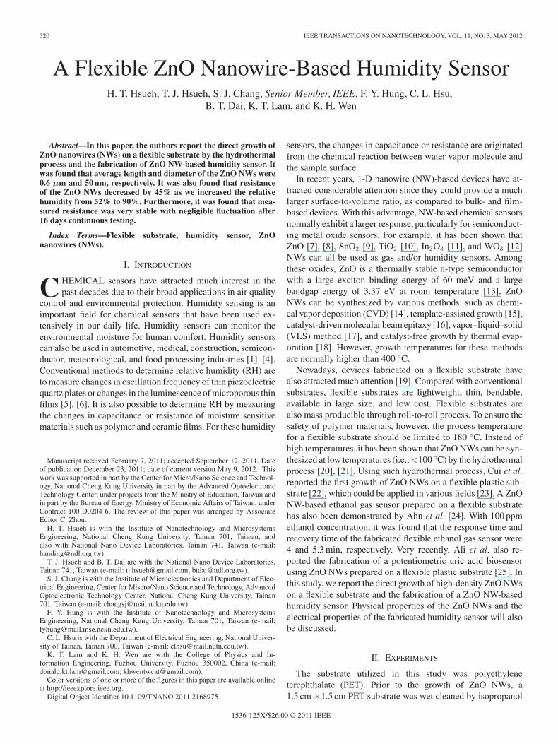
520 IEEE TRANSACTIONS ON NANOTECHNOLOGY, VOL. 11, NO. 3, MAY 2012
A Flexible ZnO Nanowire-Based Humidity SensorH. T. Hsueh, T. J. Hsueh, S. J. Chang, Senior Member, IEEE, F. Y. Hung, C. L. Hsu,
B. T. Dai, K. T. Lam, and K. H. Wen
Abstract—In this paper, the authors report the direct growth ofZnO nanowires (NWs) on a flexible substrate by the hydrothermalprocess and the fabrication of ZnO NW-based humidity sensor. Itwas found that average length and diameter of the ZnO NWs were0.6 μm and 50 nm, respectively. It was also found that resistanceof the ZnO NWs decreased by 45% as we increased the relativehumidity from 52% to 90%. Furthermore, it was found that mea-sured resistance was very stable with negligible fluctuation after16 days continuous testing.
Index Terms—Flexible substrate, humidity sensor, ZnOnanowires (NWs).
I. INTRODUCTION
CHEMICAL sensors have attracted much interest in thepast decades due to their broad applications in air quality
control and environmental protection. Humidity sensing is animportant field for chemical sensors that have been used ex-tensively in our daily life. Humidity sensors can monitor theenvironmental moisture for human comfort. Humidity sensorscan also be used in automotive, medical, construction, semicon-ductor, meteorological, and food processing industries [1]–[4].Conventional methods to determine relative humidity (RH) areto measure changes in oscillation frequency of thin piezoelectricquartz plates or changes in the luminescence of microporous thinfilms [5], [6]. It is also possible to determine RH by measuringthe changes in capacitance or resistance of moisture sensitivematerials such as polymer and ceramic films. For these humidity
Manuscript received February 7, 2011; accepted September 12, 2011. Dateof publication December 23, 2011; date of current version May 9, 2012. Thiswork was supported in part by the Center for Micro/Nano Science and Technol-ogy, National Cheng Kung University in part by the Advanced OptoelectronicTechnology Center, under projects from the Ministry of Education, Taiwan andin part by the Bureau of Energy, Ministry of Economic Affairs of Taiwan, underContract 100-D0204-6. The review of this paper was arranged by AssociateEditor C. Zhou.
H. T. Hsueh is with the Institute of Nanotechnology and MicrosystemsEngineering, National Cheng Kung University, Tainan 701, Taiwan, andalso with National Nano Device Laboratories, Tainan 741, Taiwan (e-mail:[email protected]).
T. J. Hsueh and B. T. Dai are with the National Nano Device Laboratories,Tainan 741, Taiwan (e-mail: [email protected]; [email protected]).
S. J. Chang is with the Institute of Microelectronics and Department of Elec-trical Engineering, Center for Miscro/Nano Science and Technology, AdvancedOptoelectronic Technology Center, National Cheng Kung University, Tainan701, Taiwan (e-mail: [email protected]).
F. Y. Hung is with the Institute of Nanotechnology and MicrosystemsEngineering, National Cheng Kung University, Tainan 701, Taiwan (e-mail:[email protected]).
C. L. Hsu is with the Department of Electrical Engineering, National Univer-sity of Tainan, Tainan 700, Taiwan (e-mail: [email protected]).
K. T. Lam and K. H. Wen are with the College of Physics and In-formation Engineering, Fuzhou University, Fuzhou 350002, China (e-mail:[email protected]; [email protected]).
Color versions of one or more of the figures in this paper are available onlineat http://ieeexplore.ieee.org.
Digital Object Identifier 10.1109/TNANO.2011.2168975
sensors, the changes in capacitance or resistance are originatedfrom the chemical reaction between water vapor molecule andthe sample surface.
In recent years, 1-D nanowire (NW)-based devices have at-tracted considerable attention since they could provide a muchlarger surface-to-volume ratio, as compared to bulk- and film-based devices. With this advantage, NW-based chemical sensorsnormally exhibit a larger response, particularly for semiconduct-ing metal oxide sensors. For example, it has been shown thatZnO [7], [8], SnO2 [9], TiO2 [10], In2O3 [11], and WO3 [12]NWs can all be used as gas and/or humidity sensors. Amongthese oxides, ZnO is a thermally stable n-type semiconductorwith a large exciton binding energy of 60 meV and a largebandgap energy of 3.37 eV at room temperature [13]. ZnONWs can be synthesized by various methods, such as chemi-cal vapor deposition (CVD) [14], template-assisted growth [15],catalyst-driven molecular beam epitaxy [16], vapor–liquid–solid(VLS) method [17], and catalyst-free growth by thermal evap-oration [18]. However, growth temperatures for these methodsare normally higher than 400 ◦C.
Nowadays, devices fabricated on a flexible substrate havealso attracted much attention [19]. Compared with conventionalsubstrates, flexible substrates are lightweight, thin, bendable,available in large size, and low cost. Flexible substrates arealso mass producible through roll-to-roll process. To ensure thesafety of polymer materials, however, the process temperaturefor a flexible substrate should be limited to 180 ◦C. Instead ofhigh temperatures, it has been shown that ZnO NWs can be syn-thesized at low temperatures (i.e., <100 ◦C) by the hydrothermalprocess [20], [21]. Using such hydrothermal process, Cui et al.reported the first growth of ZnO NWs on a flexible plastic sub-strate [22], which could be applied in various fields [23]. A ZnONW-based ethanol gas sensor prepared on a flexible substratehas also been demonstrated by Ahn et al. [24]. With 100 ppmethanol concentration, it was found that the response time andrecovery time of the fabricated flexible ethanol gas sensor were4 and 5.3 min, respectively. Very recently, Ali et al. also re-ported the fabrication of a potentiometric uric acid biosensorusing ZnO NWs prepared on a flexible plastic substrate [25]. Inthis study, we report the direct growth of high-density ZnO NWson a flexible substrate and the fabrication of a ZnO NW-basedhumidity sensor. Physical properties of the ZnO NWs and theelectrical properties of the fabricated humidity sensor will alsobe discussed.
II. EXPERIMENTS
The substrate utilized in this study was polyethyleneterephthalate (PET). Prior to the growth of ZnO NWs, a1.5 cm ×1.5 cm PET substrate was wet cleaned by isopropanol
1536-125X/$26.00 © 2011 IEEE
HSUEH et al.: FLEXIBLE ZnO NANOWIRE-BASED HUMIDITY SENSOR 521
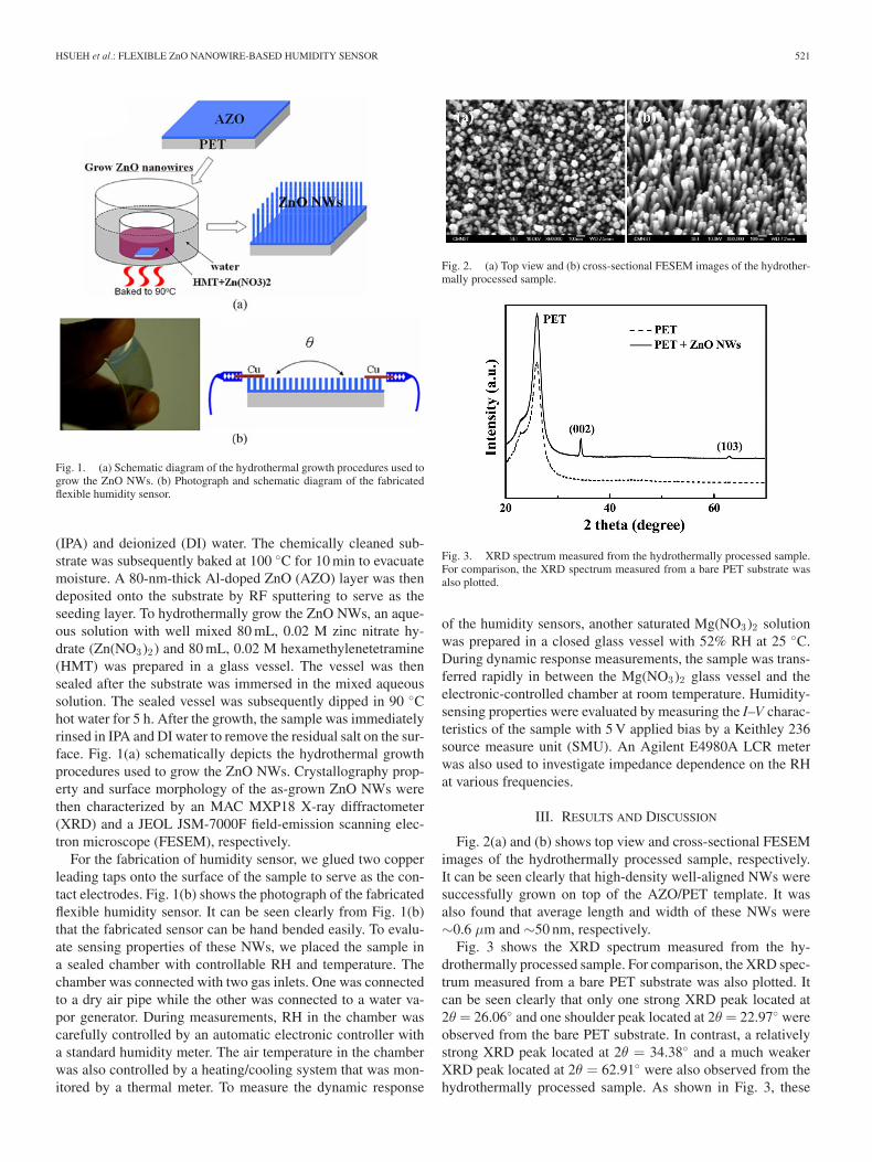
Fig. 1. (a) Schematic diagram of the hydrothermal growth procedures used togrow the ZnO NWs. (b) Photograph and schematic diagram of the fabricatedflexible humidity sensor.
(IPA) and deionized (DI) water. The chemically cleaned sub-strate was subsequently baked at 100 ◦C for 10 min to evacuatemoisture. A 80-nm-thick Al-doped ZnO (AZO) layer was thendeposited onto the substrate by RF sputtering to serve as theseeding layer. To hydrothermally grow the ZnO NWs, an aque-ous solution with well mixed 80 mL, 0.02 M zinc nitrate hy-drate (Zn(NO3)2) and 80 mL, 0.02 M hexamethylenetetramine(HMT) was prepared in a glass vessel. The vessel was thensealed after the substrate was immersed in the mixed aqueoussolution. The sealed vessel was subsequently dipped in 90 ◦Chot water for 5 h. After the growth, the sample was immediatelyrinsed in IPA and DI water to remove the residual salt on the sur-face. Fig. 1(a) schematically depicts the hydrothermal growthprocedures used to grow the ZnO NWs. Crystallography prop-erty and surface morphology of the as-grown ZnO NWs werethen characterized by an MAC MXP18 X-ray diffractometer(XRD) and a JEOL JSM-7000F field-emission scanning elec-tron microscope (FESEM), respectively.
For the fabrication of humidity sensor, we glued two copperleading taps onto the surface of the sample to serve as the con-tact electrodes. Fig. 1(b) shows the photograph of the fabricatedflexible humidity sensor. It can be seen clearly from Fig. 1(b)that the fabricated sensor can be hand bended easily. To evalu-ate sensing properties of these NWs, we placed the sample ina sealed chamber with controllable RH and temperature. Thechamber was connected with two gas inlets. One was connectedto a dry air pipe while the other was connected to a water va-por generator. During measurements, RH in the chamber wascarefully controlled by an automatic electronic controller witha standard humidity meter. The air temperature in the chamberwas also controlled by a heating/cooling system that was mon-itored by a thermal meter. To measure the dynamic response
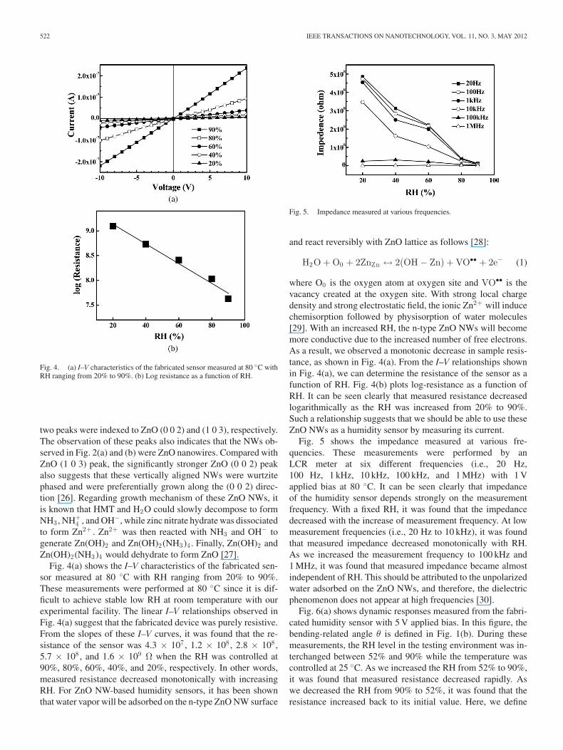
Fig. 2. (a) Top view and (b) cross-sectional FESEM images of the hydrother-mally processed sample.
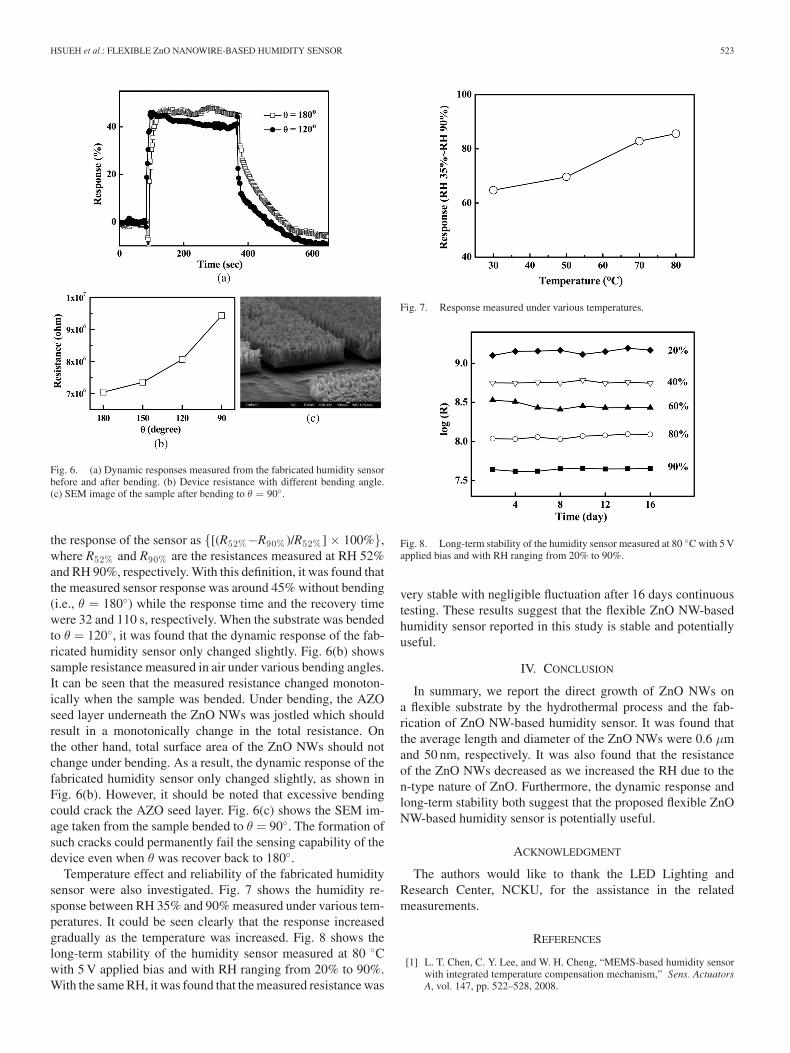
Fig. 3. XRD spectrum measured from the hydrothermally processed sample.For comparison, the XRD spectrum measured from a bare PET substrate wasalso plotted.
of the humidity sensors, another saturated Mg(NO3)2 solutionwas prepared in a closed glass vessel with 52% RH at 25 ◦C.During dynamic response measurements, the sample was trans-ferred rapidly in between the Mg(NO3)2 glass vessel and theelectronic-controlled chamber at room temperature. Humidity-sensing properties were evaluated by measuring the I–V charac-teristics of the sample with 5 V applied bias by a Keithley 236source measure unit (SMU). An Agilent E4980A LCR meterwas also used to investigate impedance dependence on the RHat various frequencies.
III. RESULTS AND DISCUSSION
Fig. 2(a) and (b) shows top view and cross-sectional FESEMimages of the hydrothermally processed sample, respectively.It can be seen clearly that high-density well-aligned NWs weresuccessfully grown on top of the AZO/PET template. It wasalso found that average length and width of these NWs were∼0.6 μm and ∼50 nm, respectively.
Fig. 3 shows the XRD spectrum measured from the hy-drothermally processed sample. For comparison, the XRD spec-trum measured from a bare PET substrate was also plotted. Itcan be seen clearly that only one strong XRD peak located at2θ = 26.06◦ and one shoulder peak located at 2θ = 22.97◦ wereobserved from the bare PET substrate. In contrast, a relativelystrong XRD peak located at 2θ = 34.38◦ and a much weakerXRD peak located at 2θ = 62.91◦ were also observed from thehydrothermally processed sample. As shown in Fig. 3, these
522 IEEE TRANSACTIONS ON NANOTECHNOLOGY, VOL. 11, NO. 3, MAY 2012
Fig. 4. (a) I–V characteristics of the fabricated sensor measured at 80 ◦C withRH ranging from 20% to 90%. (b) Log resistance as a function of RH.
two peaks were indexed to ZnO (0 0 2) and (1 0 3), respectively.The observation of these peaks also indicates that the NWs ob-served in Fig. 2(a) and (b) were ZnO nanowires. Compared withZnO (1 0 3) peak, the significantly stronger ZnO (0 0 2) peakalso suggests that these vertically aligned NWs were wurtzitephased and were preferentially grown along the (0 0 2) direc-tion [26]. Regarding growth mechanism of these ZnO NWs, itis known that HMT and H2O could slowly decompose to formNH3 , NH+
4 , and OH−, while zinc nitrate hydrate was dissociatedto form Zn2+ . Zn2+ was then reacted with NH3 and OH− togenerate Zn(OH)2 and Zn(OH)2(NH3)4 . Finally, Zn(OH)2 andZn(OH)2(NH3)4 would dehydrate to form ZnO [27].
Fig. 4(a) shows the I–V characteristics of the fabricated sen-sor measured at 80 ◦C with RH ranging from 20% to 90%.These measurements were performed at 80 ◦C since it is dif-ficult to achieve stable low RH at room temperature with ourexperimental facility. The linear I–V relationships observed inFig. 4(a) suggest that the fabricated device was purely resistive.From the slopes of these I–V curves, it was found that the re-sistance of the sensor was 4.3 × 10⁷ , 1.2 × 10⁸ , 2.8 × 10⁸ ,5.7 × 108 , and 1.6 × 10⁹ Ω when the RH was controlled at90%, 80%, 60%, 40%, and 20%, respectively. In other words,measured resistance decreased monotonically with increasingRH. For ZnO NW-based humidity sensors, it has been shownthat water vapor will be adsorbed on the n-type ZnO NW surface
Fig. 5. Impedance measured at various frequencies.
and react reversibly with ZnO lattice as follows [28]:
H2O + O0 + 2ZnZn ↔ 2(OH − Zn) + VO•• + 2e− (1)
where O0 is the oxygen atom at oxygen site and VO•• is thevacancy created at the oxygen site. With strong local chargedensity and strong electrostatic field, the ionic Zn2+ will inducechemisorption followed by physisorption of water molecules[29]. With an increased RH, the n-type ZnO NWs will becomemore conductive due to the increased number of free electrons.As a result, we observed a monotonic decrease in sample resis-tance, as shown in Fig. 4(a). From the I–V relationships shownin Fig. 4(a), we can determine the resistance of the sensor as afunction of RH. Fig. 4(b) plots log-resistance as a function ofRH. It can be seen clearly that measured resistance decreasedlogarithmically as the RH was increased from 20% to 90%.Such a relationship suggests that we should be able to use theseZnO NWs as a humidity sensor by measuring its current.
Fig. 5 shows the impedance measured at various fre-quencies. These measurements were performed by anLCR meter at six different frequencies (i.e., 20 Hz,100 Hz, 1 kHz, 10 kHz, 100 kHz, and 1 MHz) with 1 Vapplied bias at 80 ◦C. It can be seen clearly that impedanceof the humidity sensor depends strongly on the measurementfrequency. With a fixed RH, it was found that the impedancedecreased with the increase of measurement frequency. At lowmeasurement frequencies (i.e., 20 Hz to 10 kHz), it was foundthat measured impedance decreased monotonically with RH.As we increased the measurement frequency to 100 kHz and1 MHz, it was found that measured impedance became almostindependent of RH. This should be attributed to the unpolarizedwater adsorbed on the ZnO NWs, and therefore, the dielectricphenomenon does not appear at high frequencies [30].
Fig. 6(a) shows dynamic responses measured from the fabri-cated humidity sensor with 5 V applied bias. In this figure, thebending-related angle θ is defined in Fig. 1(b). During thesemeasurements, the RH level in the testing environment was in-terchanged between 52% and 90% while the temperature wascontrolled at 25 ◦C. As we increased the RH from 52% to 90%,it was found that measured resistance decreased rapidly. Aswe decreased the RH from 90% to 52%, it was found that theresistance increased back to its initial value. Here, we define
HSUEH et al.: FLEXIBLE ZnO NANOWIRE-BASED HUMIDITY SENSOR 523
Fig. 6. (a) Dynamic responses measured from the fabricated humidity sensorbefore and after bending. (b) Device resistance with different bending angle.(c) SEM image of the sample after bending to θ = 90◦.
the response of the sensor as {[(R52%−R90% )/R52% ] × 100%},where R52% and R90% are the resistances measured at RH 52%and RH 90%, respectively. With this definition, it was found thatthe measured sensor response was around 45% without bending(i.e., θ = 180◦) while the response time and the recovery timewere 32 and 110 s, respectively. When the substrate was bendedto θ = 120◦, it was found that the dynamic response of the fab-ricated humidity sensor only changed slightly. Fig. 6(b) showssample resistance measured in air under various bending angles.It can be seen that the measured resistance changed monoton-ically when the sample was bended. Under bending, the AZOseed layer underneath the ZnO NWs was jostled which shouldresult in a monotonically change in the total resistance. Onthe other hand, total surface area of the ZnO NWs should notchange under bending. As a result, the dynamic response of thefabricated humidity sensor only changed slightly, as shown inFig. 6(b). However, it should be noted that excessive bendingcould crack the AZO seed layer. Fig. 6(c) shows the SEM im-age taken from the sample bended to θ = 90◦. The formation ofsuch cracks could permanently fail the sensing capability of thedevice even when θ was recover back to 180◦.
Temperature effect and reliability of the fabricated humiditysensor were also investigated. Fig. 7 shows the humidity re-sponse between RH 35% and 90% measured under various tem-peratures. It could be seen clearly that the response increasedgradually as the temperature was increased. Fig. 8 shows thelong-term stability of the humidity sensor measured at 80 ◦Cwith 5 V applied bias and with RH ranging from 20% to 90%.With the same RH, it was found that the measured resistance was
Fig. 7. Response measured under various temperatures.
Fig. 8. Long-term stability of the humidity sensor measured at 80 ◦C with 5 Vapplied bias and with RH ranging from 20% to 90%.
very stable with negligible fluctuation after 16 days continuoustesting. These results suggest that the flexible ZnO NW-basedhumidity sensor reported in this study is stable and potentiallyuseful.
IV. CONCLUSION
In summary, we report the direct growth of ZnO NWs ona flexible substrate by the hydrothermal process and the fab-rication of ZnO NW-based humidity sensor. It was found thatthe average length and diameter of the ZnO NWs were 0.6 μmand 50 nm, respectively. It was also found that the resistanceof the ZnO NWs decreased as we increased the RH due to then-type nature of ZnO. Furthermore, the dynamic response andlong-term stability both suggest that the proposed flexible ZnONW-based humidity sensor is potentially useful.
ACKNOWLEDGMENT
The authors would like to thank the LED Lighting andResearch Center, NCKU, for the assistance in the relatedmeasurements.
REFERENCES
[1] L. T. Chen, C. Y. Lee, and W. H. Cheng, “MEMS-based humidity sensorwith integrated temperature compensation mechanism,” Sens. ActuatorsA, vol. 147, pp. 522–528, 2008.
524 IEEE TRANSACTIONS ON NANOTECHNOLOGY, VOL. 11, NO. 3, MAY 2012
[2] T. L. Yeo, T. Sun, and K. T. V. Grattan, “Fibre-optic sensor technologiesfor humidity and moisture measurement,” Sens. Actuators A, vol. 144,pp. 280–295, 2008.
[3] P. G. Su and C. P. Wang, “Flexible humidity sensor based on TiO2nanoparticles-polypyrrole-poly[3-(methacrylamino)propyl] trimethylammonium chloride composite materials,” Sens. Actuators B, vol. 129,pp. 538–543, 2008.
[4] A. Vijayan, M. Fuke, R. Hawaldar, M. Kulkarni, D. Amalnerkar, andR. C. Aiyer, “Optical fibre based humidity sensor using Co-polyanilineclad,” Sens. Actuators B, vol. 129, pp. 106–112, 2008.
[5] F. Pascal-Delannoy, B. Sorli, and A. Boyer, “Quartz crystal microbalance(QCM) used as humidity sensor,” Sens. Actuators A, vol. 84, pp. 285–291,2000.
[6] A. Erol, S. Okur, N. Yagmurcukardes, and M. C. Arikan, “Humidity-sensing properties of a ZnO nanowire film as measured with a QCM,”Sens. Actuators B, vol. 152, pp. 115–120, 2011.
[7] Z. P. Sun, L. Liu, L. Zhang, and D. Z. Jia, “Rapid synthesis of ZnOnano-rods by one-step, room-temperature, solid-state reaction and theirgas-sensing properties,” Nanotechnology, vol. 17, pp. 2266–2270, 2006.
[8] Q. Wan, Q. H. Li, Y. J. Chen, T. H. Wang, X. L. He, J. P. Li, andC. L. Lin, “Fabrication and ethanol sensing characteristics of ZnOnanowire gas sensors,” Appl. Phys. Lett., vol. 84, pp. 3654–3656, 2004.
[9] E. Comini, G. Faglia, G. Sberveglieri, Z. Pan, and Z. L. Wang, “Stable andhighly sensitive gas sensors based on semiconducting oxide nanobelts,”Appl. Phys. Lett., vol. 81, pp. 1869–1871, 2002.
[10] R. J. Wu, Y. L. Sun, C. C. Lin, H. W. Chen, and M. Chavali, “Composite ofTiO2 nanowires and Nafion as humidity sensor material,” Sens. ActuatorsB, vol. 115, pp. 198–204, 2006.
[11] A. Vomiero, S. Bianchi, E. Comini, G. Faglia, M. Ferroni, N. Poli, andG. Sberveglieri, “In2 O3 nanowires for gas sensors: morphology and sens-ing characterisation,” Thin Solid Films, vol. 515, pp. 8356–8359, 2007.
[12] K. M. Sawicka, A. K. Prasad, and P. I. Gouma, “Metal oxide nanowiresfor use in chemical sensing applications,” Sens. Lett., vol. 3, pp. 31–35,2005.
[13] N. Kumar, A. Dorfman, and J. Hahm, “Fabrication of optically enhancedZnO nanorods and microrods using novel biocatalysts,” J. Nanosci. Nan-otechnol., vol. 5, pp. 1915–1918, 2005.
[14] J. J. Wu and S. C. Liu, “Catalyst-free growth and characterization of ZnOnanorods,” J. Phys. Chem. B, vol. 106, pp. 9546–9551, 2002.
[15] Y. Li, G. W. Meng, L. D. Zhang, and F. Phillipp, “Ordered semiconductorZnO nanowire arrays and their photoluminescence properties,” Appl.Phys. Lett., vol. 76, pp. 2011–2013, 2000.
[16] Y. W. Heo, V. Varadarajan, M. Kaufman, K. Kim, D. P. Norton,F. Ren, and P. H. Fleming, “Site-specific growth of ZnO nanorods usingcatalysis-driven molecular-beam epitaxy,” Appl. Phys. Lett., vol. 81,pp. 3046–3048, 2002.
[17] C. L. Hsu, S. J. Chang, H. C. Hung, Y. R. Lin, C. J. Huang, Y. K. Tseng, andI. C. Chen, “Vertical single-crystal ZnO nanowires grown on ZnO:Ga/glasstemplates,” IEEE Tran. Nanotechnol., vol. 4, no. 6, pp. 649–654, Nov.2005.
[18] T. J. Hsueh, S. J. Chang, Y. R. Lin, S. Y. Tsai, I. C. Chen, and C. L. Hsu,“A novel method for the formation of ladder-like ZnO nanowires,” Cryst.Growth Des., vol. 6, pp. 1282–1284, 2006.
[19] P. G. Su and Y. S. Chuang, “Flexible H(2) sensors fabricated by layer-by-layer self-assembly thin film of multi-walled carbon nanotubes andmodified in situ with Pd nanoparticles,” Sens. Actuators B, vol. 145,pp. 521–526, 2010.
[20] L. Vayssieres, “Growth of arrayed nanorods and nanowires of ZnO fromaqueous solutions,” Adv. Mater., vol. 15, pp. 464–466, 2003.
[21] L. E. Greene, M. Law, J. Goldberger, F. Kim, J. D. Johnson, Y. F. Zhang,R. J. Saykally, and P. D. Yang, “Low-temperature wafer-scale productionof ZnO nanowire arrays,” Angew. Chem. Int. Ed., vol. 42, pp. 3031–3034,2003.
[22] J. B. Cui, C. P. Daghlian, U. J. Gibson, R. Pusche, P. Geithner, and L. Ley,“Low-temperature growth and field emission of ZnO nanowire arrays,” J.Appl. Phys., vol. 97, pp. 044315-1–044315-7, 2005.
[23] B. Weintraub, Z. Z. Zhou, Y. H. Li, and Y. L. Deng, “Solution synthesis ofone-dimensional ZnO nanomaterials and their applications,” Nanoscale,vol. 2, pp. 1573–1587, 2010.
[24] H. Ahn, J. H. Park, S. B. Kim, S. H. Jee, Y. S. Yoon, and D. J. Kim,“Vertically aligned ZnO nanorod sensor on flexible substrate for ethanolgas monitoring,” Electrochem. Solid-State Lett., vol. 13, pp. J125–J128,2010.
[25] S. M. U. Ali, N. H. Alvi, Z. Ibupoto, O. Nur, M. Willander, and B.Danielsson, “Selective potentiometric determination of uric acid with
uricase immobilized on ZnO nanowires,” Sens. Actuators B, vol. 152,pp. 241–247, 2011.
[26] M. Purica, E. Budianu, E. Rusu, M. Danila, and R. Gavrila, “Opticaland structural investigation of ZnO thin films prepared by chemical vapordeposition (CVD),” Thin Solid Films, vol. 403–404, pp. 485–488, 2002.
[27] X. D. Yan, Z. W. Li, R. Q. Chen, and W. Gao, “Template growth of ZnOnanorods and microrods with controllable densities,” Cryst. Growth. Des.,vol. 8, pp. 2406–2410, 2008.
[28] W. P. Tai and J. H. OH, “Humidity sensing behaviors of nanocrystallineAl-doped ZnO thin films prepared by sol-gel process,” J. Mater. Sci.,Mater. Electron., vol. 13, pp. 391–394, 2002.
[29] S. R. Morrison, “Semiconductor gas sensors,” Sens. Actuators, vol. 2,pp. 329–341, 1982.
[30] V. Bondarenka, S. Grebinskij, S. Mickevicius, V. Volkov, andG. Zacharova, “Thin-films of poly-vanadium-molybednum acid as startingmaterials for humidity sensors,” Sens. Actuators B, vol. 28, pp. 227–231,1995.
H. T. Hsueh received the B.S. degree in physicsfrom the National Chang Hua University of Educa-tion, Changhua, Taiwan, in 1998, and the M.S. de-gree in physics from National Tsing Hua University,Hsinchu, Taiwan, in 2000. He is currently working to-ward the Ph.D. degree at the Institute of Nanotechnol-ogy and Microsystems Engineering, National ChengKung University, Tainan, Taiwan.
Since 2002, he has been an Engineer with the Na-tional Nano Device Laboratories, Tainan.
T. J. Hsueh received the M.S. degree in electrical en-gineering from the National Kaohsiung University ofApplied Sciences, Kaohsiung, Taiwan, in 2004, andthe Ph.D. degree in microelectronics from NationalCheng Kung University (NCKU), Tainan, Taiwan, in2008.
From September 2008 to January 2009, he wasa Postdoctoral Researcher with the Advanced Opto-electronic Technology Center, NCKU. He is currentlya Postdoctoral Researcher with the National NanoDevice Laboratories, Tainan. His current research in-
terests include nanoscaled 1-D semiconductors and solar cells.
S. J. Chang (M’06–SM’10) was born in Taipei,Taiwan, on January 17, 1961. He received the B.S.degree from the National Cheng Kung University(NCKU), Tainan, Taiwan in 1983, the M.S. degreefrom the State University of New York, Stony Brookin 1985, and the Ph.D. degree from the Universityof California, Los Angeles, in 1989, all in electricalengineering.
From 1989 to 1992, he was a Research Scientistwith Nippon Telegraph and Telephone (NTT) BasicResearch Laboratories, Musashino, Tokyo, Japan. He
joined the Department of Electrical Engineering, NCKU, in 1992 as an Asso-ciate Professor, where he was promoted to Full Professor in 1998. He is currentlythe Deputy Director of the Center for Micro/Nano Science and Technology, theDeputy Director of the Advanced Optoelectronic Technology Center, and theDirector of the Institute of Microelectronics, NCKU. He was a Royal SocietyVisiting Scholar with the University of Wales, Swansea, U.K., from January1999 to March 1999, a Visiting Scholar with the Research Center for AdvancedScience and Technology, University of Tokyo, Japan from July 1999 to February2000, a Visiting Scholar with the Institute of Microstructural Science, NationalResearch Council, Ottawa, Canada, from August 2001 to September 2001, aVisiting Scholar with the Institute of Physics, Stuttgart University, Germanyfrom August 2002 to September 2002, and a Visiting Scholar with the Facultyof Engineering, Waseda University, Japan from July 2005 to September 2005.His current research interests include semiconductor physics, optoelectronicdevices, and nanotechnology.
Dr. Chang is the recipient of the outstanding research award from the Na-tional Science Council, Taiwan in 2004. He is also an Honorary Professor ofChangchun University of Science and Technology, China.
HSUEH et al.: FLEXIBLE ZnO NANOWIRE-BASED HUMIDITY SENSOR 525
F. Y. Hung received the B.S. degree from I-ShouUniversity, Kaohsiung, Taiwan and the M.S. degreefrom the National Pingtung University of Science andTechnology, Pingtung, Taiwan, in 1995 and 1997,respectively, both in mechanical engineering, andthe Ph.D. degree in materials science and engineer-ing from National Cheng Kung University (NCKU),Tainan, Taiwan, in 2002.
He served as a Postdoctoral Researcher with theDepartment of Materials Science and Engineering,NCKU, from 2002 to 2007. He is currently an Assis-
tant Professor with the Institute of Nanotechnology and Microsystems Engineer-ing, NCKU. His research interests include anode/cathode of lithium batteries,optoelectronic thin films, micro/nano wires, and microelectronic materials.
C. L. Hsu was born in Taipei, Taiwan, in 1973. He re-ceived the B.S. degree in electronic engineering fromChung Yuan Christian University, Chung-Li, Taiwan,in 1996, the M.S. degree from the Department ofElectronic Engineering, National Taiwan Universityof Science and Technology, Taipei, Taiwan, in 1998,and the Ph.D. degree from the Department of Elec-trical Engineering, National Cheng Kung University,Tainan, Taiwan, in 2005.
From 2000 to 2003, he was an Engineerwith Taiwan Semiconductor Manufacturing Com-
pany (TSMC). From 2003 to 2005, he was with the Material Research Lab-oratories, Industrial Technology Research Institute, where he was involved inthe development of the synthesis of nanoscale materials. From 2005 to 2006,he was an Assistant Professor with the Department of Electrical and Elec-tronic Engineering, Mingchi University of Technology, Taipei. He is currentlyan Associate Professor with the Department of Electrical Engineering, NationalUniversity of Tainan, Tainan. His current research interests include nanoscale1-D semiconductors.
B. T. Dai received the B.S. degree in electrical en-gineering from National Cheng Kung University,Tainan, Taiwan, in 1968, and the M.S. degree from theInstitute of Electronics, National Chiao-Tung Univer-sity, Hsinchu, Taiwan, in 1970. He received the Ph.D.degree in electrical engineering from the Universityof Southern California, Los Angeles, in 1987.
He has been the Vice President of Taiwan MoselCorporation with responsibility of wafer foundry,quality control, and production control since 1990–1992. Since 1992, he has been a Researcher with Na-
tional Nano Device Laboratory, Tainan, Taiwan. His research interests includenanotechnology fabrication, nanoscience and technology, and VLSI technology.
K. T. Lam was born in Hong Kong on February23, 1965. He received the B.S. degree in mechanicalengineering from National Cheng Kung University,Tainan, Taiwan, in 1987, and the Ph.D. degree inmechanical engineering from National Sun Yat-SenUniversity, Kaohsiung, Taiwan, in 1993.
He is currently a Full Professor and AcademicLeader of the College of Physics and InformationEngineering, Fuzhou University, Fuzhou, China. Healso serves as the Director of the Institute of CreativeIndustries Research, Fuzhou University. He is also
a Visiting Professor of the School of Software, Xiamen University, Xiamen,China. His current research interests include nanotechnology, innovation design,and Fractal theory.
K. H. Wen was born in Taiwan in 1964. He receivedthe Doctorate degree from the National School ofDesign, Vic., Australia, in 2007.
He is currently a Full Professor and AcademicLeader of the College of Physics and InformationEngineering, Fuzhou University, Fuzhou, China. Healso serves as the Associate Director of the Institute ofCreative Industries Research, Fuzhou University. Heis also a Visiting Professor of the Xiamen University,Xiamen, China.