Urchin-like nanowire array: a strategy for high-performance ZnO-based electrode utilized in...
9
Urchin-like nanowire array: a strategy for high-performance ZnO-based electrode utilized in photoelectrochemistry† Hoang Nhat Hieu, Nguyen Quoc Dung, Jimin Kim and Dojin Kim * The electrodes in photoelectrochemical cells responsible for the generation of hydrogen and oxygen by water splitting have been intensively studied because of their high photon-to-electron conversion efficiency. The morphology of nanostructures with these high-efficiency electrodes was systematically compared with the morphology of ZnO structures with vertically aligned nanorod arrays (NA), hollow hemisphere arrays (HA), urchin-like (UL) nanorod arrays, and thin films (TF). The UV-vis light absorption, photoresponse (current–voltage characteristics in the dark and under light), and photoelectrochemistry of the electrodes were measured. The highest photon-to-electron conversion efficiency of 65% at a specific UV wavelength for an electrode with a ZnO UL structure was derived from the UL morphology of high light-trapping efficiency and carrier collection efficiency. The UL morphology also produced a photon-to-electron conversion efficiency of 4.5% under a solar simulator by CdS-sensitization of the ZnO UL electrode. The value was the highest observed thus far among the ZnO-based electrodes. We demonstrated that photoresponse measurement is a practical and simple technique for the estimation of the photon-to-electron conversion efficiency of an electrode. 1 Introduction Photoelectrolysis of water is a method that produces hydrogen by solar energy. Since Fujishima and Honda 1 reported water splitting in a TiO 2 photoelectrode in 1972, various semicon- ducting metal oxides have been investigated for electrode use in photoelectrochemical (PEC) cells. 2–6 The thermodynamics of the technique require semiconductors with an energy gap greater than 1.23 eV as the electrode materials, and the solar spectrum requires materials with smaller energy gaps for higher efficiency in sunlight absorption. However, in practice, the technique requires materials with much higher energy gaps (approxi- mately >1.7 eV to 2.0 eV), and the majority of wavelengths in the visible region are not absorbed by the electrode, producing a maximum solar energy that is less than 10%. 7 Various strat- egies in material engineering have been tested to obtain a higher absorption efficiency, particularly in the visible range. These strategies include employing materials with smaller bandgap energies, doping to form intra-gap energy levels, and hybridization with small bandgap semiconductors. 2–5 Another important strategy is the control of material morphology. Micro- and nano-structural morphologies have been intensively studied to enhance the absorption of sunlight for application in solar cells. 8–17 The morphology of nanorod arrays shows enhanced absorption of sunlight theoretically and experimentally in terms of the range of absorption wavelength and layer thickness. 9,10 The enhancement in the absorption efficiency is attributed to high light trapping caused by the low reection and transmittance in the vertical nanorods. 12,18 Tapered nanorods and domed-tip arrays also enhance efficiency by absorption through wide angles of light incidence. 12–14 The above nanostructures for solar cells are mostly studied with Si. Similar light-absorption enhancement effects for PEC elec- trodes have been studied with branched nanorod structures of TiO 2 and ZnO. 8,15–17 Carrier collection efficiency is another crit- ical issue that needs to be addressed for PEC electrodes to achieve high efficiency during water splitting, just like in solar cells. However, no systematic studies on carrier transport behavior have been conducted thus far. We report that the urchin-like (UL) ZnO nanowire structure recently developed in this lab, 19 omnidirectionally grown with ZnO nanowires on the surfaces of the ZnO hemispheres, is a morphology suitable for use as an electrode of high photon-to- electron conversion efficiency in PEC cells. ZnO nanostructural electrodes composed of a hemisphere array (HA), vertically grown nanorods, omnidirectionally grown urchin-like nano- rods, and thin lm electrodes were systematically compared with respect to light absorption, carrier transport, and PEC performance. We demonstrated that the omnidirectional growth morphology of nanowires (UL structure) is efficient in Department of Materials Science and Engineering, Chungnam National University, Daejeon, 305-764, Rep. of Korea. E-mail: [email protected]; Fax: +82 42 823 7648; Tel: +82 42 821 6639 † Electronic supplementary information (ESI) available. See DOI: 10.1039/c3nr00889d Cite this: Nanoscale, 2013, 5, 5530 Received 20th February 2013 Accepted 2nd April 2013 DOI: 10.1039/c3nr00889d www.rsc.org/nanoscale 5530 | Nanoscale, 2013, 5, 5530–5538 This journal is ª The Royal Society of Chemistry 2013 Nanoscale PAPER
-
Upload
independent -
Category
Documents
-
view
2 -
download
0
Transcript of Urchin-like nanowire array: a strategy for high-performance ZnO-based electrode utilized in...

Nanoscale
PAPER
Department of Materials Science and Engi
Daejeon, 305-764, Rep. of Korea. E-mail: d
Tel: +82 42 821 6639
† Electronic supplementary informa10.1039/c3nr00889d
Cite this: Nanoscale, 2013, 5, 5530
Received 20th February 2013Accepted 2nd April 2013
DOI: 10.1039/c3nr00889d
www.rsc.org/nanoscale
5530 | Nanoscale, 2013, 5, 5530–553
Urchin-like nanowire array: a strategy forhigh-performance ZnO-based electrode utilized inphotoelectrochemistry†
Hoang Nhat Hieu, Nguyen Quoc Dung, Jimin Kim and Dojin Kim*
The electrodes in photoelectrochemical cells responsible for the generation of hydrogen and oxygen by
water splitting have been intensively studied because of their high photon-to-electron conversion
efficiency. The morphology of nanostructures with these high-efficiency electrodes was systematically
compared with the morphology of ZnO structures with vertically aligned nanorod arrays (NA), hollow
hemisphere arrays (HA), urchin-like (UL) nanorod arrays, and thin films (TF). The UV-vis light absorption,
photoresponse (current–voltage characteristics in the dark and under light), and photoelectrochemistry
of the electrodes were measured. The highest photon-to-electron conversion efficiency of 65% at a
specific UV wavelength for an electrode with a ZnO UL structure was derived from the UL morphology
of high light-trapping efficiency and carrier collection efficiency. The UL morphology also produced a
photon-to-electron conversion efficiency of 4.5% under a solar simulator by CdS-sensitization of the
ZnO UL electrode. The value was the highest observed thus far among the ZnO-based electrodes. We
demonstrated that photoresponse measurement is a practical and simple technique for the estimation
of the photon-to-electron conversion efficiency of an electrode.
1 Introduction
Photoelectrolysis of water is a method that produces hydrogenby solar energy. Since Fujishima and Honda1 reported watersplitting in a TiO2 photoelectrode in 1972, various semicon-ducting metal oxides have been investigated for electrode use inphotoelectrochemical (PEC) cells.2–6 The thermodynamics of thetechnique require semiconductors with an energy gap greaterthan 1.23 eV as the electrode materials, and the solar spectrumrequires materials with smaller energy gaps for higher efficiencyin sunlight absorption. However, in practice, the techniquerequires materials with much higher energy gaps (approxi-mately >1.7 eV to 2.0 eV), and the majority of wavelengths in thevisible region are not absorbed by the electrode, producing amaximum solar energy that is less than �10%.7 Various strat-egies in material engineering have been tested to obtain ahigher absorption efficiency, particularly in the visible range.These strategies include employing materials with smallerbandgap energies, doping to form intra-gap energy levels, andhybridization with small bandgap semiconductors.2–5
Another important strategy is the control of materialmorphology. Micro- and nano-structural morphologies have
neering, Chungnam National University,
[email protected]; Fax: +82 42 823 7648;
tion (ESI) available. See DOI:
8
been intensively studied to enhance the absorption of sunlightfor application in solar cells.8–17 The morphology of nanorodarrays shows enhanced absorption of sunlight theoretically andexperimentally in terms of the range of absorption wavelengthand layer thickness.9,10 The enhancement in the absorptionefficiency is attributed to high light trapping caused by the lowreection and transmittance in the vertical nanorods.12,18
Tapered nanorods and domed-tip arrays also enhance efficiencyby absorption through wide angles of light incidence.12–14 Theabove nanostructures for solar cells are mostly studied with Si.Similar light-absorption enhancement effects for PEC elec-trodes have been studied with branched nanorod structures ofTiO2 and ZnO.8,15–17 Carrier collection efficiency is another crit-ical issue that needs to be addressed for PEC electrodes toachieve high efficiency during water splitting, just like in solarcells. However, no systematic studies on carrier transportbehavior have been conducted thus far.
We report that the urchin-like (UL) ZnO nanowire structurerecently developed in this lab,19 omnidirectionally grown withZnO nanowires on the surfaces of the ZnO hemispheres, is amorphology suitable for use as an electrode of high photon-to-electron conversion efficiency in PEC cells. ZnO nanostructuralelectrodes composed of a hemisphere array (HA), verticallygrown nanorods, omnidirectionally grown urchin-like nano-rods, and thin lm electrodes were systematically comparedwith respect to light absorption, carrier transport, and PECperformance. We demonstrated that the omnidirectionalgrowth morphology of nanowires (UL structure) is efficient in
This journal is ª The Royal Society of Chemistry 2013

Paper Nanoscale
light trapping, particularly in the visible region, and in carriercollection. This result was derived by measuring the photo-current of the electrodes in air, which is also a simple techniqueto estimate the photon-to-electron conversion efficiency of theelectrode in the PEC cell. Motivated by the highest photon-to-electron conversion efficiency at a UV light wavelength (UV-CE)with the optimized ZnO UL electrode, we further sensitized theelectrodes with a narrow bandgap material for more efficientvisible-light absorption.
2 Experiment2.1 Preparation of ZnO–NA, ZnO–HA, and ZnO–UL lms
A thin Zn layer was sputter-deposited on the substrates, fol-lowed by oxidation at 500 �C in air for 2 h to serve as the seedlayer for the hydrothermal synthesis of vertically alignedZnO–NAs. For the hydrothermal synthesis, a mixture of 0.04 Mof aqueous solution that included zinc nitrate [Zn(NO3)2$6H2O]and hexamethylenetetramine (C6H12N4) (1 : 1 ratio) wasprepared based on our previous research.19 The seededsubstrates were placed in the solution at 90 �C to allow ZnO–NAgrowth. The nanorod length was controlled by varying thegrowth time (1, 2, 3, 4, 6, and 12 h). The ZnO–NA structures werewashed with deionized water and dried by nitrogen ow drying.
The ZnO–UL structures were formed through the samehydrothermal synthesis method described above for the ZnO–NA growth, but on hollow ZnO HAs synthesized on SiO2/Si andITO substrates following the process developed in this labora-tory, described in detail in ref. 19. To summarize, a powderysubstance composed of polystyrene (PS) spheres with diametersof �1.5 mm was rst synthesized as described in ref. 29, andthen dispersed in ethanol (1 wt%) to form the PS sphere solu-tion. The PS spheres were coated on the SiO2/Si and ITOsubstrates by a drop-casting method and dried on a hot plateat 90 �C. Zn was subsequently sputter-deposited on the PSspheres/SiO2/Si and PS spheres/ITO substrates. Zn was depos-ited only on the top half of the PS sphere arrays because of theshadowing effect. The oxidation of the Zn/PS sphere substratesin air at 500 �C for 2 h burned out the PS cores and converted theZn–HAs to ZnO–HAs on the SiO2/Si and ITO substrates. TheZnO–HAs formed though this method also served as the seedlayer for further hydrothermal synthesis of the ZnO–UL elec-trode samples or the vertical growth of ZnO nanorods on theZnO–HA seed layers formed by the ZnO–UL structures. Thenanorod length was again controlled by varying the growth time(1, 2, 3, 4, 6, and 12 h).
2.2 Preparation of CdS/ZnO–NA and CdS/ZnO–UL lms
The ZnO–NA and ZnO–UL structures were chemically grown for4 h, and those that exhibited the best photoconversion prop-erties were further decorated with CdS layers for higherabsorption in the range of visible light.30,31 The CdS nano-crystals were directly grown on the ZnO nanorod surfaces byincubating the ZnO–NA/ITO and ZnO–UL/ITO electrodes in anaqueous solution of 10 mM of Cd (NO3)2$4H2O and 10 mM of
This journal is ª The Royal Society of Chemistry 2013
C2H5NS at room temperature for 15, 30, 60, and 90 min, fol-lowed by rinsing with deionized water and blow-drying with N2.
2.3 Characterization of the lms
The crystalline structures of the synthesized ZnO–NA and ZnO–UL were examined by XRD (Rigaku, D/MAX-RC) with Cu Karadiation. The morphology of the synthesized structures wasexamined with a eld-emission scanning electron microscope(JEOL, JSM-700F) and a transmission electron microscope(JEOL, JEM-1010). A UV-vis spectrophotometer (S-3100, SCINCOCo.) was utilized to measure the optical absorption spectra.
2.4 PEC measurements
PEC properties were measured with a three-electrode electro-chemical analyzer (Potentiostat/Galvanostat Model 263A). Thefabricated nanostructural lms formed on ITO were utilized asthe working electrode, the Pt-grid as the counter electrode, andthe Hg2Cl2/Hg in saturated KCl as the reference electrode. Theelectrolyte utilized for the ZnO structures consisted of 0.01 M ofNa2SO4, whereas that for the CdS/ZnO structures consisted of 1M of Na2S. A UV light source with an intensity of 0.3 mW cm�2
and a wavelength of 365 nm (Z169609 – E-Series UV Lamp,output 4 W, AC input 230 V) was utilized to measure the pho-toconversion efficiency of the structures by measuring thephotocurrent while varying the potential at a sweeping rate of 10mV s�1. A visible light source, a 150 W Xe lamp with theintensity of 100 mW cm�2 passing through an AM 1.5 G lter,was also employed to evaluate the photoconversion efficiency ofthe CdS/ZnO electrodes. The area of the working electrodeexposed to the electrolyte was xed at 0.25 cm2 by nonconduc-tive epoxy coating. The photoconversion efficiency was calcu-lated with the following equation:
hð%Þ ¼ 100� Jp�Erev � Eapp
�
I0(1)
where Jp is the photocurrent density (mA cm�2), I0 is the powerdensity of the incident light (0.3 and 100 mW cm�2), and Erev isthe standard state-reversible potential (1.23 V vs. NHE). Eapp ¼Emeas� Eaoc is the applied potential, where Emeas is the electrodepotential of the working electrode (vs. SCE) under illuminationand Eaoc is the electrode potential of the same working electrodeunder open circuit conditions.15 The I–V characteristics of theelectrodes in the dark and under the UV light were measuredthrough the nanostructures formed on bar-type Pt electrodeswith a multimeter (Keithley 2400). The photoresponse of theelectrodes was dened as S¼ (A� A0)/A0, where A0 and A are thecurrents measured with UV light off and on, respectively.
3 Results and discussion3.1 Structure and morphology
The morphologies of the synthesized ZnO structures with (a)thin lm (TF), (b) hollow HA, (c and d) vertically alignednanorod array (NA), and (e and f) UL nanorod array structuresare compared in Fig. 1. The ZnO–NA and ZnO–UL structuresshow the 4 h growth of nanorods in the solution. Comparisons
Nanoscale, 2013, 5, 5530–5538 | 5531

Fig. 1 Morphology of (a) ZnO–TF, (b) ZnO–HA, (c and d) ZnO–NA, and (e and f) ZnO–UL structures.
Nanoscale Paper
with the other growth times are shown in Fig. S1 and S2.† Thecomparison reveals that the diameters of ZnO nanorodsincreased with synthesis time, whereas the density of thenanorods decreased. This morphological change in relation togrowth time occurred because most of the nanorods were notnormally grown into the substrate but quasi-vertically with tiltangles q < 30� in the ZnO–NA structure as illustrated in Fig. 2a.When a growing rod encounters another growing rod, the rodfront is blocked by another rod and the lengthwise growthstops. Thus, the rod density continues to decrease as thesynthesis continues, and the length and diameter of thesurviving rods increase. As a result, the average size of the spaceamong the nanorods increases with time. This “block-and-survive” control of nanorod density also occurs with the ZnO–
Fig. 2 Schematic of the growth morphology of NA, HA, and UL structures showinglight absorption and generation and diffusional transport of carriers. Region b has thcomponents for the conduction channel b are also shown for each of the structuresrod path, respectively).
5532 | Nanoscale, 2013, 5, 5530–5538
UL structures, where growth omnidirectionally occurs with tiltangles from 0� to almost 90� (Fig. 1e, f, 2c and S2†). The ULmorphology was obtained by the quasi-vertical growth of ZnOnanorods on hemispherical ZnO seed layers in Fig. 2b. Thehollow ZnO–HAs have a uniform size of about 1.5 mm indiameter, and the nanorods growing upon them are distributedin diameters of tens of nanometers. The 3D hierarchical UL andNA structures are divided into regions a and b, as shown inFig. 2a. Both regions contribute to light absorption and carriergeneration, but b forms an effective conduction channel thatcarries the collected electrons to the external circuit. Theequivalent circuit components forming the conduction channelb for NA, HA, and UL structures are also shown in Fig. 2. Thenanorods were grown on ZnO seed layers with thin lms in the
that the growth stops because of the tilted growth of the nanorods. Region a is fore additional role of carrier conductor in the external circuitry. The equivalent circuit(gseed, gHA, gR-R: conductance of the seed-layer film, hemisphere array, and rod-to-
This journal is ª The Royal Society of Chemistry 2013

Paper Nanoscale
NA structures; therefore, conduction occurred through twoparallel channels of thin lm (seed layer) and rod-to-rodcontacts. Similarly, the UL structure has two parallel channels:the hollow HA and the rod-to-rod contacts. No clear a regionwas observed in the HA structure and in the thin lms.
The nanorod diameters of the NA and UL structures did notdiffer markedly, and the morphologies of the NA and the ULstructures merged when the nanorods were grown for a verylong time, for example, 12 h. This result is understandablebecause only the rods growing with relatively small tilt angleswill survive until the late stage of the synthesis if the rod densityis controlled by the block-and-survive mode. We demonstratehow this convergence in morphology between the NA and ULstructures with prolonged synthesis time results in the conver-gence of the measured properties. The difference between thestructures was remarkable at an intermediate synthesis time of4 h; thus, the investigations were carried out with the NA and ULsamples grown for 4 h unless otherwise specied.
Fig. S3† summarizes the structural properties of the chemi-cally synthesized ZnO nanorods measured by XRD and TEM. Allthe synthesized HA, NA, and UL structures had a hexagonalwurtzite ZnO structure with lattice parameters of a¼ 3.25 A andc¼ 5.21 A [JCPDS 36-1451]. The high-resolution TEM image andselected area diffraction pattern showed that the nanorods weresingle crystals grown along the [0001] direction, as determinedby interplanar spacing of 0.52 nm corresponding to the (0002)plane of the hexagonal ZnO.
Fig. 3 (a) Light transmission (T) and (b) reflectance (R) spectra of the ZnO–TF,ZnO–HA, ZnO–NA, and ZnO–UL structures. (c) Absorption was calculated by 100T� R. All the measurements are for the normal direction of the samples.
3.2 Optical absorption properties
The optical properties of the ZnO nanostructure lms wereexamined by UV-vis spectroscopy of transmittance (T) andreectance (R) in the normal direction for the samples ofZnO–TF, ZnO–HA, ZnO–NA, and ZnO–UL. The absorption (A)was calculated by A ¼ 100T � R, as summarized in Fig. 3.16
The light absorption rate of the various ZnO lms exhibitedan absorption edge around 380 nm, conrming previousreports.20–22 With regard to the UV light of the energy greaterthan the bandgap, all the array structures (HA, NA, and UL)revealed zero reectance that can be compared with the 5%reectance of the thin lm structure. The enhanced antireec-tion effect with the 3D nanorod structures18 and the texturedsurfaces13,14 was thus conrmed. The difference in reectancecaused by geometry was at most �5%. The nite transmittanceof 30% to 35% with the TF and HA structures was caused by thethinness of the lms (�70 nm). Therefore, the almost completeabsorption (�98%) with the NA and UL structures suggests thatthe nanorod array of �1 mm length is sufficient to collect thetransmitting light.
The difference in absorption among the structures wasmore pronounced in the visible region where the ZnO bandgapis greater than the incident light energies. Compared with thealmost zero absorption with the thin lm geometry, niteabsorption with the nanostructure arrays was observed. Thereectance rates were 17%, 5%, 3%, and 0% at 550 nm wave-length for TF, HA, NA, and UL, respectively, as shown in Fig. 3b.This result conrms the nite enhanced antireection effects
This journal is ª The Royal Society of Chemistry 2013
with the textured surface (HA) and 3D hierarchical structures(NA and UL). However, the effect decreases as the wavelengthincreases. The zero reectance of the UL structure throughoutthe entire wavelength region is remarkable. The absorptionrates were 2%, 18%, 25%, and 60% at 550 nm and 0%, 2%, 9%,and 51% at 700 nm for TF, HA, NA, and UL, respectively, asshown in Fig. 3c. The UL structure exhibited remarkableenhanced absorption at a longer wavelength. The practicallyzero reectance over the visible range is correlated with therandom orientation of the nanorods with the omnidirectionalgrowth morphology that randomizes and multiplies light
Nanoscale, 2013, 5, 5530–5538 | 5533

Nanoscale Paper
scattering. However, the mechanism through which suchenhanced trapping of visible lights leads to enhanced absorp-tion with large bandgap energy is still unclear. The signicantabsorption enhancement with UL rather than NA suggests thatthe broad tilt angles of the nanorods and the frequent exposureof the nanorod walls to the incident light enhance the photo-excitation of the valence electrons via the surface defect traps.This model is effective when the defects are concentrated on thesurfaces and when more than two photons contribute to theexcitation of an electron. The decrease in absorption efficiencywith longer wavelength qualitatively coincides with this photo-generation model but remains an issue that needs to beexplored intensively.
3.3 Photo-conduction properties
High light absorption and transport without loss of the photo-generated carriers is necessary for PEC cell electrodes to achievehigh efficiency. The transport of photo-generated carriers ispresented in Fig. 4. The carrier collection efficiencies among thestructures are distinguished from the light absorption effi-ciencies. The ohmic I–V curves measured through biasing in thedark and under UV light (l ¼ 365 nm) for the ZnO–UL structureis shown in Fig. 4a. The other array structures of HA and NAalso exhibited good ohmic behavior (not shown). Fig. 4b
Fig. 4 (a) I–V characteristics of ZnO–UL measured in the dark and under UV light,showed similar ohmic behavior. (b) The current at 1 V shown in (a) is plotted for HA, Nand photoresponse variation in the ZnO–UL electrodes grown at different nanoroexplained in Fig. 2.
5534 | Nanoscale, 2013, 5, 5530–5538
summarizes the currents measured at 1 V biasing in the darkand under UV light for the HA, NA, and UL structures.
First, the dark currents owing through the electrode lmsare different in terms of magnitude, leading to a conductanceratio of HA : NA : UL ¼ 1 : 20 : 400. This is the ratio of theeffective thickness of the conduction channels (b) composed ofthe same materials. According to the equivalent circuits of thestructures shown in Fig. 2, the thick channel of the NA structurecompared with the TF structure (similar UL compared with HA)consists of the rod-to-rod contacts (gR-R) established during theinitial block-and-survive growth stage. The comparison showsthat the conductance of HA and TF (gHA and gseed, respectively)or the thickness of their channels is relatively small.
Second, the 20-fold channel thickness of the UL structureindicates that gR-R in the UL structure is 20 times greater thangR-R in the NA structure. This thick channel of the UL structureis explained by the following: (i) the nanorods grow above andbelow the ZnO hemisphere layers because the solution leaksfrom the hemisphere wall during nanorod synthesis;19 and (ii)the rods growing with large tilt angles (which may be q > 30�)soon hit other rods and/or hemispheres and stop growing,which establish thicker rod-to-rod contact channels. Inconclusion, the high conductance or the thick channel of the ULstructure was established by numerous rod-to-rod contacts
illustrating the ohmic property of the electrode. ZnO–HA and ZnO–NA structuresA, and UL. The photoresponses of the samples are also compared. (c) Dark currentd lengths. (d) Model for the photocurrent measurement. Regions a and b are
This journal is ª The Royal Society of Chemistry 2013

Paper Nanoscale
created during the solution growth of nanorods on the hollowHA with a broad distribution of the tilt angles. This explanationis conrmed by Fig. 4c, which shows the current measurementsaer varying the nanorod growth time in the UL structure. Thecurrent increases from �10�8 A for HA to �10�5 A for UL. The�2 mmnanorod lengths reveal the thickening of the channel (orthe increasing rod-to-rod contacts) as the growth progresses.The current saturation at prolonged growth indicates theabortion of the rod-to-rod encounters, which happens becauseonly the nanorods with small q survive and grow until the latestage without the rod-to-rod contacts.
Based on the analysis of the channel conductance of thestructures, we observe that the photoresponse [dened by theincrement in % of current because of UV light (l ¼ 365 nm)illumination with respect to the dark current] of ZnO–UL was�210%, which is much higher than that of ZnO–NA (75%) andZnO–HA (47%), as shown in Fig. 4b. Fig. 2 and 4d show that thelight is absorbed in regions a and b of the structure. Photo-carriers are generated, but the geometry of the structuresconnes the conduction channel to region b. Therefore, thephoto-carriers generated in region a need to be transported toregion b to contribute to the current.
The comparison of the photoresponses of the electrodestructures is tantamount to the comparison of the photo-generated excess carriers that reached the transport channel
Fig. 5 Electrochemical properties of the ZnO–UL structures with different nanorod lefficiency (UV-CE) were measured as a function of applied potential (vs. SCE) under UComparison of the UV-CE of the best ZnO–TF, HA, NA, and UL structures.
This journal is ª The Royal Society of Chemistry 2013
and were normalized to the equilibrium carriers in the channel.Photoresponse is a combined result of the generation of carriersby light absorption and their transport to the conductionchannel. If the photoresponse purely reects the efficiency oflight absorption with 100% quantum efficiency, the photo-response of the UL and NA structures should be about 1.5 timesthat of HA in Fig. 3c (because the absorption efficiency ratio isTF : HA : NA : UL¼ 65 : 65 : 99 : 99 at 365 nm). The 4.5- and 2.8-fold higher photoresponse of UL compared with HA and NA,respectively, cannot be explained solely by the difference in thelight absorption. The HA and TF structures do not distinguishregion a and region b, but the NA and UL do. The additionalcarriers transported from region a to region b produced highphotoresponses. This phenomenon led to high carrier collec-tion efficiencies for the 3D hierarchical structures of NA and UL.The difference between the UL and NA structures is attributedto the morphology of the omnidirectionally grown nanorods,which provides more exposure of the nanorod root regions anda larger exposed surface area. The condition provides thetransport channel shorter diffusion lengths for higher photo-generated carrier concentrations. Given the array of quasi-vertical nanorods in the NA structure, light absorption wouldoccur more likely near the tip of the nanorods. The electrontransport distance would thus be longer, leading to lower elec-tron collection efficiency.
engths measured under UV light. (a) Photocurrent density and (b) photoconversionV light. Plots of (a) and (b) are redrawn in (c) against the nanorod growth time. (d)
Nanoscale, 2013, 5, 5530–5538 | 5535

Nanoscale Paper
Fig. 4c shows that the photoresponse of the UL structureincreased with growth time (showing its maximum at 4 hgrowth) because of the increasing surface area of nanorods withhigh light absorption. This increase indicates that the supplyrate of photo-carriers from region a is higher than the channelthickening rate as the growth proceeds. However, at prolongedgrowth, the morphology of the UL structure with long nanorodsapproaches that of the NA structure (Fig. S1f and S2f†), andregion a moves to the top of the nanorods when the channelthickening is stopped. The lowered light absorption efficiencyowing to the degraded omnidirectional morphology andincreased diffusion length reduces the photoresponse withthe 12 h-grown UL structure. In conclusion, the highest pho-toresponse from the 4 h-grown UL structure is realized byenhanced light absorption and carrier collection efficiencies byoptimizing the nanorod length of the omnidirectional growthmorphology. The results suggest that the electron diffusionlength in the ZnO nanorods is on the order of hundreds ofnanometers.
3.4 PEC properties of ZnO and CdS/ZnO nanostructures
We directly measure the PEC properties of the electrode struc-tures in a solution by water splitting. The photoresponsemeasurement discussed above is a simple and useful techniqueto estimate in advance the PEC performance of the electrodes.The PEC properties of the ZnO–TF, ZnO–HA, ZnO–NA, andZnO–UL structures were examined again under UV light (l ¼365 nm). The anodic photocurrents measured with varyingpotential biases on the UL structures grown with differentsynthesis times are shown in Fig. 5a. A similar series of curveswas obtained for the ZnO–NA series (not shown). The
Fig. 6 (a–d) FESEM images of CdS/ZnO–UL structures as the dipping time was variabsorption spectra and solar photoconversion efficiency as a function of applied po
5536 | Nanoscale, 2013, 5, 5530–5538
photoconversion efficiencies under UV light (UV-CEs) arecalculated in Fig. 5a through eqn (1). The results are shown inFig. 5b. The maximum photocurrent density and UV-CEs for theelectrodes with different growth times are summarized inFig. 5c. The Figure presents the highest photon-to-electronconversion efficiency of 65% at growth of 4 h. This value wascompared with the values of the other electrodes of ZnO–NA (3 hgrowth), ZnO–HA, and ZnO–TF (Fig. 5d).
The observed 65% efficiency of the ZnO–UL structure is thehighest value obtained from ZnO lms and nanostructures.23,24
The UV-CE ratios of the structures are HA : NA : UL ¼11.5% : 23% : 65% ¼ 18 : 35 : 100, which roughly coincide withthe photoresponse measurements (47% : 75% : 210% ¼22 : 36 : 100). This result is expected because all the photo-generated electron–hole pairs contribute to the electrochemicalreactions that occur at the electrode–electrolyte interface duringwater splitting. The photoresponse measurement with an elec-trode in ambient air may thus be a convenient tool to estimatethe photon-to-electron conversion efficiency of the ZnO elec-trodes in the PEC cell of a liquid solution. The result also leadsto the conclusion that the high photon-to-electron conversionefficiency of the UL structure as a PEC cell electrode is thecombined effect of high light trapping and carrier collectionefficiencies achieved by the omnidirectional growth of thenanorods.
Motivated by the success of previous studies, we attemptedto create a practical PEC cell electrode of high photon-to-elec-tron conversion efficiency by incorporating a narrow bandgapmaterial, namely, CdS (2.4 eV) with ZnO (3.37 eV), to enhancefurther the absorbance in the visible-light region of the solarspectrum.30,31 The CdS sensitization time in the solution for theZnO–TF, NA, and UL structures was varied to achieve the
ed; 15, 30, 60, and 90 min, respectively. (e) and (f) show the corresponding UV-vistential (vs. SCE).
This journal is ª The Royal Society of Chemistry 2013
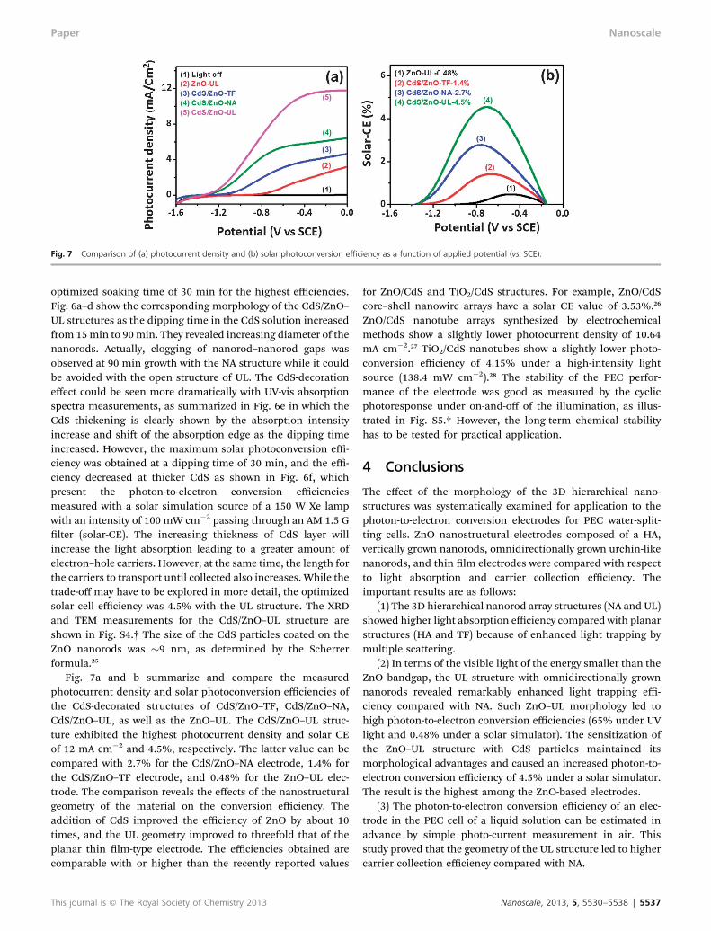
Fig. 7 Comparison of (a) photocurrent density and (b) solar photoconversion efficiency as a function of applied potential (vs. SCE).
Paper Nanoscale
optimized soaking time of 30 min for the highest efficiencies.Fig. 6a–d show the corresponding morphology of the CdS/ZnO–UL structures as the dipping time in the CdS solution increasedfrom 15min to 90min. They revealed increasing diameter of thenanorods. Actually, clogging of nanorod–nanorod gaps wasobserved at 90 min growth with the NA structure while it couldbe avoided with the open structure of UL. The CdS-decorationeffect could be seen more dramatically with UV-vis absorptionspectra measurements, as summarized in Fig. 6e in which theCdS thickening is clearly shown by the absorption intensityincrease and shi of the absorption edge as the dipping timeincreased. However, the maximum solar photoconversion effi-ciency was obtained at a dipping time of 30 min, and the effi-ciency decreased at thicker CdS as shown in Fig. 6f, whichpresent the photon-to-electron conversion efficienciesmeasured with a solar simulation source of a 150 W Xe lampwith an intensity of 100 mW cm�2 passing through an AM 1.5 Glter (solar-CE). The increasing thickness of CdS layer willincrease the light absorption leading to a greater amount ofelectron–hole carriers. However, at the same time, the length forthe carriers to transport until collected also increases. While thetrade-off may have to be explored in more detail, the optimizedsolar cell efficiency was 4.5% with the UL structure. The XRDand TEM measurements for the CdS/ZnO–UL structure areshown in Fig. S4.† The size of the CdS particles coated on theZnO nanorods was �9 nm, as determined by the Scherrerformula.25
Fig. 7a and b summarize and compare the measuredphotocurrent density and solar photoconversion efficiencies ofthe CdS-decorated structures of CdS/ZnO–TF, CdS/ZnO–NA,CdS/ZnO–UL, as well as the ZnO–UL. The CdS/ZnO–UL struc-ture exhibited the highest photocurrent density and solar CEof 12 mA cm�2 and 4.5%, respectively. The latter value can becompared with 2.7% for the CdS/ZnO–NA electrode, 1.4% forthe CdS/ZnO–TF electrode, and 0.48% for the ZnO–UL elec-trode. The comparison reveals the effects of the nanostructuralgeometry of the material on the conversion efficiency. Theaddition of CdS improved the efficiency of ZnO by about 10times, and the UL geometry improved to threefold that of theplanar thin lm-type electrode. The efficiencies obtained arecomparable with or higher than the recently reported values
This journal is ª The Royal Society of Chemistry 2013
for ZnO/CdS and TiO2/CdS structures. For example, ZnO/CdScore–shell nanowire arrays have a solar CE value of 3.53%.26
ZnO/CdS nanotube arrays synthesized by electrochemicalmethods show a slightly lower photocurrent density of 10.64mA cm�2.27 TiO2/CdS nanotubes show a slightly lower photo-conversion efficiency of 4.15% under a high-intensity lightsource (138.4 mW cm�2).28 The stability of the PEC perfor-mance of the electrode was good as measured by the cyclicphotoresponse under on-and-off of the illumination, as illus-trated in Fig. S5.† However, the long-term chemical stabilityhas to be tested for practical application.
4 Conclusions
The effect of the morphology of the 3D hierarchical nano-structures was systematically examined for application to thephoton-to-electron conversion electrodes for PEC water-split-ting cells. ZnO nanostructural electrodes composed of a HA,vertically grown nanorods, omnidirectionally grown urchin-likenanorods, and thin lm electrodes were compared with respectto light absorption and carrier collection efficiency. Theimportant results are as follows:
(1) The 3D hierarchical nanorod array structures (NA and UL)showed higher light absorption efficiency compared with planarstructures (HA and TF) because of enhanced light trapping bymultiple scattering.
(2) In terms of the visible light of the energy smaller than theZnO bandgap, the UL structure with omnidirectionally grownnanorods revealed remarkably enhanced light trapping effi-ciency compared with NA. Such ZnO–UL morphology led tohigh photon-to-electron conversion efficiencies (65% under UVlight and 0.48% under a solar simulator). The sensitization ofthe ZnO–UL structure with CdS particles maintained itsmorphological advantages and caused an increased photon-to-electron conversion efficiency of 4.5% under a solar simulator.The result is the highest among the ZnO-based electrodes.
(3) The photon-to-electron conversion efficiency of an elec-trode in the PEC cell of a liquid solution can be estimated inadvance by simple photo-current measurement in air. Thisstudy proved that the geometry of the UL structure led to highercarrier collection efficiency compared with NA.
Nanoscale, 2013, 5, 5530–5538 | 5537

Nanoscale Paper
(4) The morphology of omnidirectionally grown nanorods onhemisphere substrates provided an environment of randomlight incidence angles and multiple scattering, leading tohigh light trapping and carrier collection efficiencies. Themorphology also produced a thick channel of high conduc-tance, leading to high current density in the PEC cell. Thisoccurrence is a morphological improvement over the conven-tional vertically aligned nanorods morphology, applicable ingeneral to any material system.
Acknowledgements
This research was supported by the WCU (R32-20026) and theBasic Research program (No. 2012R1A1A4A01011671) of theMinistry of Education, Science and Technology of Korea.
Notes and references
1 A. Fujishima and K. Honda, Nature, 1972, 238, 37–38.2 R. Abe and J. Photochem, J. Photochem. Photobiol., C, 2010,11, 179–209.
3 Y. Lin, G. Yuan, R. Liu, S. Zhou, S. W. Sheehan and D. Wang,Chem. Phys. Lett., 2011, 507, 209–215.
4 H. M. Chen, C. K. Chen, R. S. Liu, L. Zhang, J. Zhang andD. P. Wilkinson, Chem. Soc. Rev., 2012, 41, 5654–5671.
5 A. Kudo and Y. Miseki, Chem. Soc. Rev., 2009, 38, 253–278.
6 T. Bak, J. Nowotny, M. Rekas and C. C. Sorrell, Int. J.Hydrogen Energy, 2002, 27, 991–1022.
7 F. E. Osterloh and B. A. Parkinson, MRS Bull., 2011, 36,17–22.
8 Y. Li and J. Z. Zhang, Laser Photonics Rev., 2009, 4, 517–528.9 M. D. Kelzenberg, S. W. Boettcher, J. A. Petykiewicz,D. B. Turner-Evans, M. C. Putnam, E. L. Warren,J. M. Spurgeon, R. M. Briggs, N. S. Lewis and H. A. Atwater,Nat. Mater., 2010, 9, 239–244.
10 R. Yu, Q. Lin, S. F. Leung and Z. Fan, Nano Energy, 2012, 1,57–72.
11 S. H. Ko, D. Lee, H. W. Kang, K. H. Nam, J. Y. Yeo, S. J. Hong,C. P. Grigoropoulos and H. J. Sung, Nano Lett., 2011, 11, 666–671.
12 L. Lu and G. Chen, Nano Lett., 2007, 7, 3249–3252.
5538 | Nanoscale, 2013, 5, 5530–5538
13 J. Zhu, C. M. Hsu, Z. Yu, S. Fan and Y. Cui, Nano Lett., 2010,10, 1979–1984.
14 J. Zhu, Z. Yu, G. F. Burkhard, C. M. Hsu, S. T. Connor, Y. Xu,Q. Wang, M. McGehee, S. Fan and Y. Cui, Nano Lett., 2009, 9,279–282.
15 J. Shi, Y. Hara, C. Sun, M. A. Anderson and X. Wang, NanoLett., 2011, 11, 3413–3419.
16 I. S. Cho, Z. Chen, A. J. Forman, D. R. Kim, P. M. Rao,T. F. Jaramillo and X. Zheng, Nano Lett., 2011, 11, 4978–4984.
17 Y. Qiu, K. Yan, H. Deng and S. Yang, Nano Lett., 2012, 12,407–413; Fan and Y. Cui, Nano Lett., 2009, 9, 279–282.
18 B. Silke, L. Diedenhofen, G. Vecchi, R. E. Algra, A. Hartsuiker,O. L. Muskens, G. Immink, E. P. A. M. Bakkers, W. L. Vos andJ. G. Rivas, Adv. Mater., 2009, 21, 973–978.
19 H. N. Hieu, N. M. Vuong, H. Jung, D. M. Jang, D. Kim, H. Kimand S.-K. Hong, J. Mater. Chem., 2012, 22, 1127–1134.
20 S. Cho, J. W. Jang, J. S. Lee and K. H. Lee, CrystEngComm,2010, 12, 3929–3935.
21 M. F. Ogawa, Y. Natsume, T. Hirayama and H. Sakata,J. Mater. Sci. Lett., 1990, 9, 1354–1356.
22 S. A. Studenikin, N. Golego and M. Cocivera, J. Appl. Phys.,1998, 83, 2104–2111.
23 B. P. T. Landberg, J. Inst. Electr. Eng., 1958, 2964E, 908.24 X. Yang, A. Wolcott, G. Wang, A. Sobo, R. C. Fitzmorris,
F. Qian, J. Zhang and Y. Li, Nano Lett., 2009, 9, 2331–2336.
25 M. Shi, X. Pan, W. Qiu, D. Zheng, M. Xu and H. Chen, Int. J.Hydrogen Energy, 2011, 36, 15153–15159.
26 Y. Tak, S. Hong, J. Lee and K. Yong, J. Mater. Chem., 2009, 19,5945–5951.
27 X. Qi, G. She, Y. Liu, L. Mu and W. Shi, Chem. Commun.,2012, 48, 242–244.
28 W. T. Sun, Y. Yu, H. Y. Pan, X. F. Gao, Q. Chen andL. M. Peng, J. Am. Chem. Soc., 2008, 130, 1124–1125.
29 Z. Xiao, A. Wang and D. P. Kim, J. Mater. Chem., 2010, 20,2853–2857.
30 D. Liu and P. V. Kamat, J. Phys. Chem., 1993, 97, 10769–10773.
31 N. Z. Bao, L. Shen, T. Takata, K. Domen, A. Gupta,K. Yanagisawa and C. A. Grimes, J. Phys. Chem. C, 2007,111, 17527–17534.
This journal is ª The Royal Society of Chemistry 2013