Nanowire photoelectrochemistry - eScholarship
98
1 Nanowire photoelectrochemistry Jiao Deng 1 , Yude Su 2, § , Dong Liu 3 , Peidong Yang 2,4,5,6,* , Bin Liu 3,* , Chong Liu 1,* 1 Department of Chemistry and Biochemistry, University of California, Los Angeles, Los Angeles, CA 90095, USA 2 Department of Chemistry, University of California, Berkeley, Berkeley, CA 94720, USA 3 School of Chemical and Biomedical Engineering, Nanyang Technological University, Singapore 637459, Singapore 4 Materials Sciences Division, Lawrence Berkeley National Laboratory, Berkeley, CA 94720, USA 5 Department of Materials Science and Engineering, University of California, Berkeley, CA 94720, USA 6 Kavli Energy NanoScience Institute, Berkeley, CA 94720, USA * To whom correspondence may be addressed. Email: [email protected] (P. Y.); [email protected] (B. L.); [email protected] (C.L.).
-
Upload
khangminh22 -
Category
Documents
-
view
0 -
download
0
Transcript of Nanowire photoelectrochemistry - eScholarship
1
Nanowire photoelectrochemistry
Jiao Deng1, Yude Su2,§, Dong Liu3, Peidong Yang2,4,5,6,*, Bin Liu3,*, Chong Liu1,*
1 Department of Chemistry and Biochemistry, University of California, Los Angeles, Los
Angeles, CA 90095, USA 2 Department of Chemistry, University of California, Berkeley, Berkeley, CA 94720, USA
3 School of Chemical and Biomedical Engineering, Nanyang Technological University,
Singapore 637459, Singapore 4 Materials Sciences Division, Lawrence Berkeley National Laboratory, Berkeley, CA 94720,
USA 5 Department of Materials Science and Engineering, University of California, Berkeley, CA
94720, USA 6 Kavli Energy NanoScience Institute, Berkeley, CA 94720, USA
* To whom correspondence may be addressed. Email: [email protected] (P. Y.);
[email protected] (B. L.); [email protected] (C.L.).
2
Abstract
Recent applications of photoelectrochemistry at the semiconductor/liquid interface provide a
renewable route of mimicking natural photosynthesis and yielding chemicals from sunlight, water,
and air. Nanowires, defined as one-dimensional nanostructures, exhibit multiple unique features
for photoelectrochemical applications and promise better performance as compared to their bulk
counterparts. This review aims to provide a summary for the use of semiconductor nanowires in
photoelectrochemistry. After a tutorial-type introduction of nanowires and photoelectrochemistry,
the summary strives to provide answers to the following questions: 1) How can we interface
semiconductor nanowires with other building blocks for enhanced photoelectrochemical responses?
2) How are nanowires utilized for photoelectrochemical half reactions? 3) What are the techniques
that allow us to obtain fundamental insights of photoelectrochemistry at single-nanowire level? 4)
What are the design strategies for an integrated nanosystem that mimics a closed cycle in artificial
photosynthesis? We postulate that this summary will help the readers to evaluate the features of
nanowires for photoelectrochemical applications. A comprehensive understanding of nanowires
in photoelectrochemistry will promote the sustainable development of solar-powered chemical
plants that will benefit our society in the long run.
3
Table of contents Page
1. Introduction 5
1.1 Concept of nanowires and nanomaterials 6
1.2 Principle of photoelectrochemistry 7
1.3 Evaluation of photoelectrochemical performance 9
1.4 Potential benefits of nanowires in photoelectrochemistry 11
1.5 Design considerations for nanowire photoelectrochemistry 16
2. Functionalized semiconductor nanowires for photoelectrochemistry 21
2.1 A survey of building blocks in photoelectrochemistry 21
2.2 Coupling nanowires with light co-absorbers 23
2.2.1 Surface bound molecules and complexes 23
2.2.2 Metal nanostructures 25
2.2.3 Semiconductor nanoparticles 29
2.3 Coupling nanowires with catalysts for chemical reactions 32
2.3.1 Molecular/cluster as catalysts 33
2.3.2 Inorganic materials as catalysts 35
2.3.3 Biological moieties as catalysts 38
3. Nanowires for the half reactions in photoelectrochemistry 42
3.1 Nanowire for oxidative photoelectrochemistry 43
3.1.1 Photoelectrochemical water oxidation 43
3.1.2 Photoelectrochemical oxidation of organics and biomass conversion 48
3.2 Nanowire for reductive photoelectrochemistry 49
3.2.1 Photoelectrochemical hydrogen evolution 50
3.2.2 Photoelectrochemical reduction of carbon dioxide 53
3.2.3 Photoelectrochemical and photocatalytic reduction of dinitrogen 57
4. Fundamentals of photoelectrochemistry at single-nanowire level 60
4.1 Single-nanowire photoelectrochemistry 60

4
4.2 Single-molecule, single-particle fluorescence spectroscopy 63
5. Integrated nanosystems for a closed cycle 66
5.1 Mimicking the microscopic assembly of natural photosynthesis 66
5.2 Integrated artificial photosynthesis and its design principle 68
6. Conclusion and outlooks 72
Author information 75
Corresponding authors 75
ORCID 75
Present Address 75
Notes 75
Biographies 76
Acknowledgement 78
References 79
5
1. Introduction
Energy and environmental sustainability, originated at large from the reliance of fossil fuels in
our society, are two of the major challenges that our humanity is facing. The sunlight irradiating
the Earth’s surface provides immense energy, roughly 105 terawatts (TW), which far exceeds the
20~40 TW of global power consumption expected by 2050.1-5 Therefore, efficient utilization of
solar energy provides a renewable route to alleviate the energy and environmental issues associated
from the extensive use of traditional fossil fuels.1,6 However, as solar energy is intermittent,1,2
efficient conversion and storage of solar energy is a critical component in a sustainable energy
future. Since the photoelectric effect discovered by Edmond Becquerel,7 researchers have made
much progress in the capture and conversion of solar energy into valuable and important assets.8-
11 In addition to the photovoltaic (PV) effect that converts sunlight into electricity,8,11 the
photoelectrochemical (PEC) effect, the light-initiated charge separation and subsequent redox
reaction at the semiconductor/liquid interface (Figure 1), provides an important pathway that
directly stores solar energy in chemical bonds, particularly in the form of chemical fuels including
hydrocarbons and dihydrogen.1-3,10 PEC effect is capable to address the issue of intermittence in
sunlight, facilitate the transportation of the “fixed” solar energy, and provide backup power during
the supply interruption of electricity.12 However, in order to achieve an efficient and economical
solar conversion by PEC technology, a variety of factors has to be considered and optimized
simultaneously: light absorption, separation and transportation of photo-generated charge carriers,
carriers extraction for chemical reactions, component integration into an integrated system, as well
as the cost of scalable module manufacturing. While a successful PEC-based artificial
photosynthetic approach invites the participation from different disciplines, one of the concepts
that introduces additional degrees of freedom in system optimization is nanomaterials and
particularly a one-dimensional nanowire morphology,13-16 thanks to the beneficial properties that
have been demonstrated from recent literature.4,15,17
In this review, we aim to summarize the research of nanowires that utilizes PEC effects to store
solar energy into chemical bonds, which was proposed as early as 2002.18 Other important PEC-
6
related technologies, for example the dye-sensitized solar cells (DSSCs) that convert solar energy
into electricity other than chemicals, are not discussed in detail here and alternative reviews are
suggested.19,20 Our narration starts from an introduction that includes the concept of nanowires,
the principles of photoelectrochemistry, the figure-of-merits for the performance of a PEC device,
and the potential benefits in PEC applications with the use of nanowires. As an efficient and
effective PEC device requires the integration and optimization of multiple components, the second
part of our review will focus on different strategies of interfacing semiconductor nanowires with
other building blocks that may be needed in artificial photosynthesis. We propose to illustrate how
the nanowire morphology can benefit the integration of multiple components in the system. These
successful integrations will lead to the discussion of nanowire photoelectrodes in the third part of
this review, which will be categorized based on the half reactions that are involved in a solar-to-
chemical process. Such an application-oriented discussion is proposed to provide the readers a
comprehensive landscape of current developments in nanowire photoelectrochemistry. The fourth
part of this review will focus on the studies at single-nanowire level for PEC applications, which
yields insights of photoelectrochemistry at microscopic scale. Last, we will discuss current
progress of applying semiconductor nanowires to construct an integrated nanosystem for an
artificial photosynthetic process. As compared to the cases that only a half-reaction is concerned,
the integrated nanosystem demands a distinguishably different design principle for optimal
performance, which will be illustrated in this section. Overall, we postulate that this review will
help the readers to evaluate the features of nanowire photoelectrochemistry. A comprehensive
understanding of nanowires in photoelectrochemistry will promote the sustainable development of
solar-powered chemical plants that will benefit our society in the long run.
1.1 Concept of nanowires and nanomaterials
Nanowire is a type of nanostructure that possesses aspect ratio large than one. Since the 1990s,
there have been increasing interests in investigating nanowires. A significant amount of
understanding about nanowires has been obtained, thanks to their tunable physical and chemical
properties.14,21-26 Compared to their bulk counterparts, nanowires exhibit distinct characteristics
7
and subsequently advantages in many practical applications.14,22,23 First, it is possible to fine-tune
the radial dimensions of nanowires and render the nanowire diameters comparable or smaller than
the characteristic lengths for various applications, including the wavelength of photons, the mean
free path of phonons, and the diffusion lengths of photoexcited carriers.25,27 Such a unique feature
leads the observed changes of physical properties in nanowires, which have been reported in
different sub-disciplines of physics and chemistry.19,24,26 In addition, nanowire morphology
possesses large surface-to-volume ratios and subsequently abundant active sites, which is
beneficial for chemical reactions.22 The large surface area also renders nanowires a suitable
platform to interface with biological moieties, yielding inorganic | biological nanohybrids with
functionalities unfound in the individual components.14,22 Thanks to such favorable properties that
nanowire morphology exhibits, a myriad of synthetic and fabrication techniques have been
developed for the preparation of nanowires with high fidelity and targeted functionality.21-23,28
Collectively, the concept of nanowire morphology have introduced many different applications in
optoelectronics,24,29-31 energy,19,20,32 catalysis,3,17,18 and biotechnology.33-35
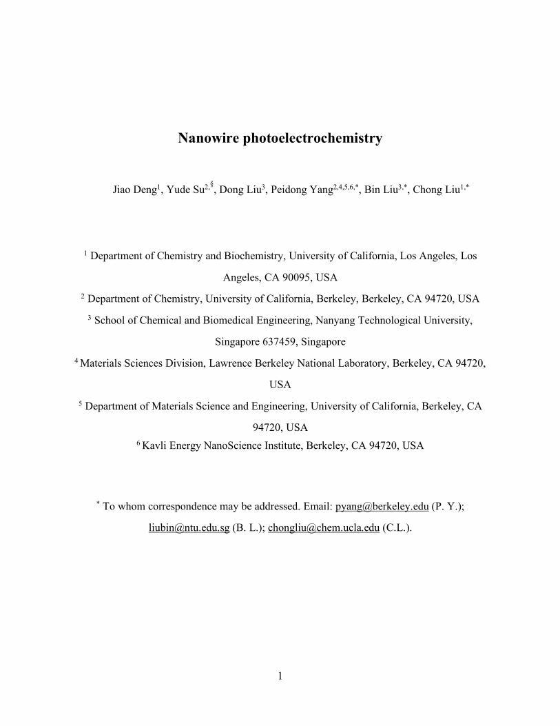
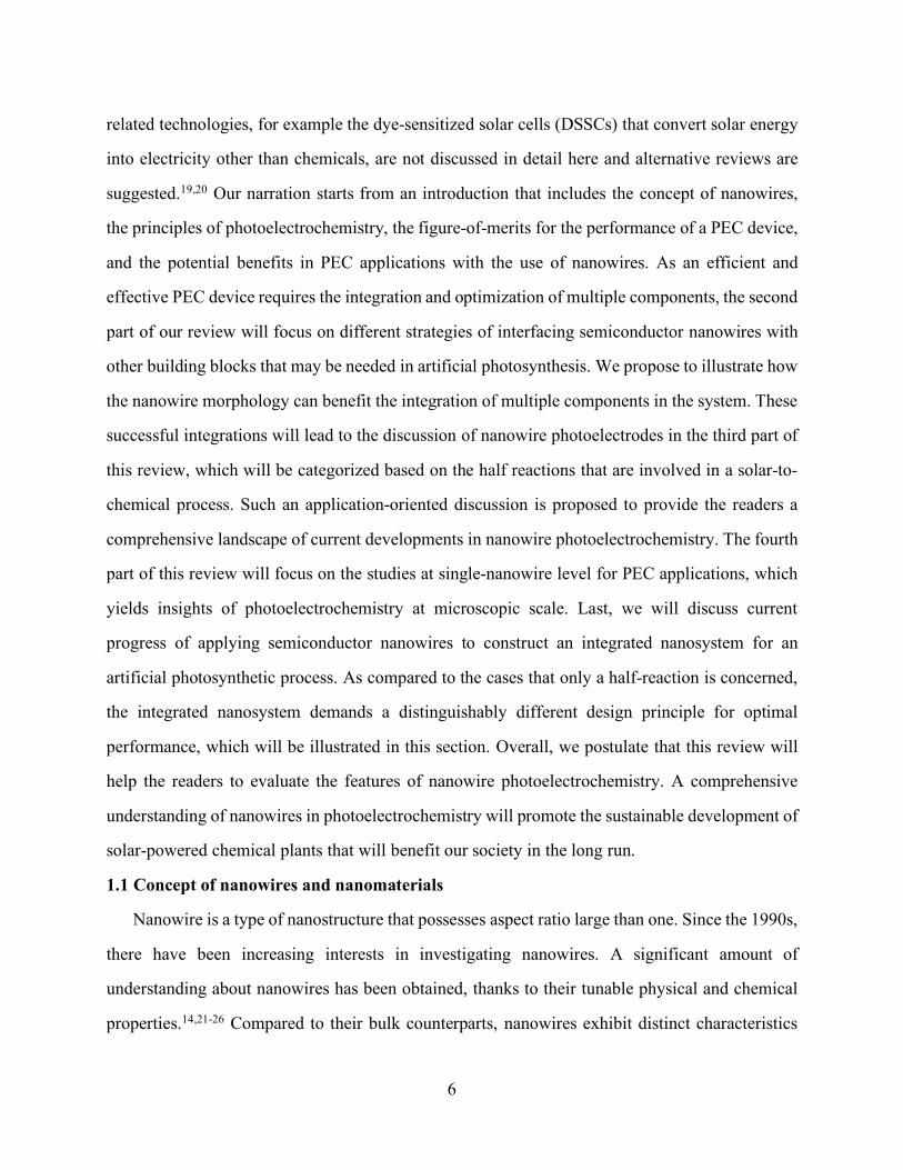
1.2 Principle of photoelectrochemistry
Photoelectrochemistry is an optoelectronic effect that occurs at the interface of a
semiconductor material and the liquid electrolyte (Figure 1a). Detailed information of the
photoelectrochemistry per se have been discussed extensively in previous literature8,16,36 and only
general description is provided here. When a semiconductor is in contact with liquid electrolyte,
the differences of Fermi levels between the semiconductor and electrolyte will lead to the band
bending at the interface as well as the establishment of a built-in electric field.8,36 Under photon
irradiation, additional electron-hole pairs (e‒/h+) are generated and spatial separation of these
photo-excited carriers takes place thanks to the presence of the built-in electric field as well as the
relatively high mobility of these carriers. Among these electron-hole pairs, the photoexcited
minority carriers move towards the semiconductor/electrolyte interface, while the majority carriers
travel through the bulk of semiconductor. A redox half-reaction that would not happen in the
absence of photon irradiation is initiated, thanks to the accumulation of photo-excited minority
8
carriers. In the case of n-type semiconductor, termed as a photoanode, a upward band-bending
leads to the accumulation of photo-generated holes for a oxidative half-reaction, while a downward
bending occurs in a p-type semiconductor (a photocathode) with the accumulation of photo-
generated electrons for a reductive half-reaction (Figure 1a). In practice, two sorts of
configurations are possible depending on the fate of these photo-generated majority carriers: 1) a
photoelectrode in which the bulk of the semiconductor is connected to an external electric circuit
and the majority carriers from photoexcitation contribute to a measurable photocurrent; 2) a
particulate form in which no external electric circuit is present and the majority carriers eventually
transport to the semiconductor/electrolyte interface for another redox half-reaction, usually with
the presence of a sacrificial chemicals termed as electron/hole scavengers. Both configurations are
viable for a solar-driven chemical production with their own unique pros and cons. The particulate
variant is considered to be of lower cost comparably, thanks to the simplicity in its design as well
as the low operational expenditure that may incur in a photo-reactor.37,38 On the other hand,
photoelectrodes enjoy a possibly more effective charge-separation under solar irradiation, as well
as the output of a photocurrent that allows for a more flexible design of the overall system. As the
oxidation and reduction occur on separate electrodes in the configuration of photoelectrode, the
backward reactions between the products of oxidation and reduction, termed as back reactions, are
mitigated. This implies that the photoelectrode configuration may have a more straightforward
design principle as only one of the half-reactions needs to be considered at a time.38
9
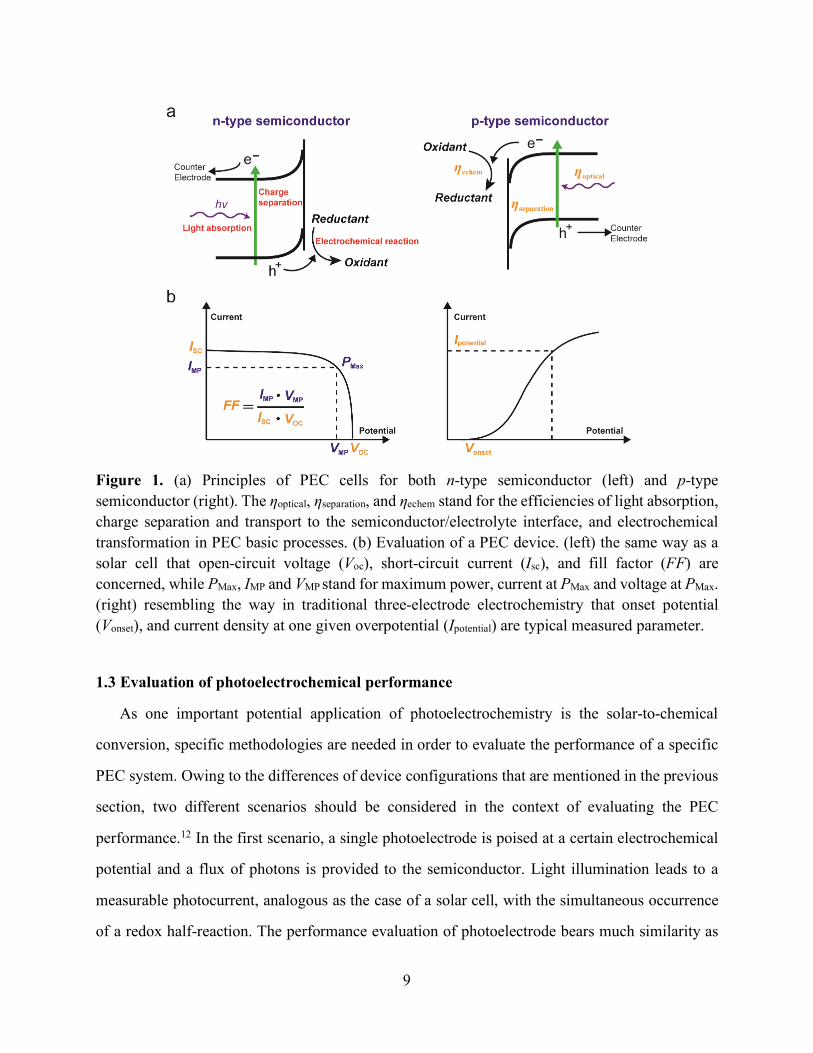
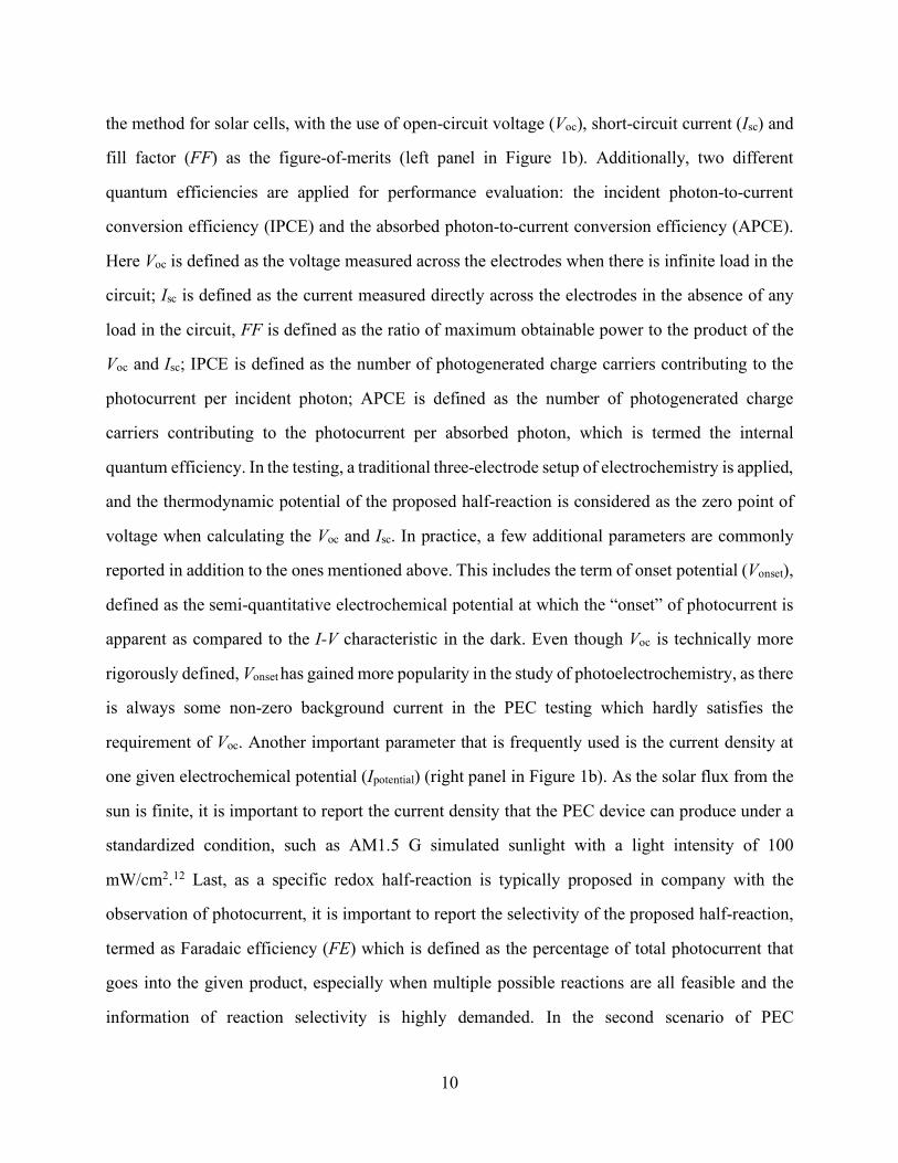
Figure 1. (a) Principles of PEC cells for both n-type semiconductor (left) and p-type semiconductor (right). The ηoptical, ηseparation, and ηechem stand for the efficiencies of light absorption, charge separation and transport to the semiconductor/electrolyte interface, and electrochemical transformation in PEC basic processes. (b) Evaluation of a PEC device. (left) the same way as a solar cell that open-circuit voltage (Voc), short-circuit current (Isc), and fill factor (FF) are concerned, while PMax, IMP and VMP stand for maximum power, current at PMax and voltage at PMax. (right) resembling the way in traditional three-electrode electrochemistry that onset potential (Vonset), and current density at one given overpotential (Ipotential) are typical measured parameter.
1.3 Evaluation of photoelectrochemical performance
As one important potential application of photoelectrochemistry is the solar-to-chemical
conversion, specific methodologies are needed in order to evaluate the performance of a specific
PEC system. Owing to the differences of device configurations that are mentioned in the previous
section, two different scenarios should be considered in the context of evaluating the PEC
performance.12 In the first scenario, a single photoelectrode is poised at a certain electrochemical
potential and a flux of photons is provided to the semiconductor. Light illumination leads to a
measurable photocurrent, analogous as the case of a solar cell, with the simultaneous occurrence
of a redox half-reaction. The performance evaluation of photoelectrode bears much similarity as
10
the method for solar cells, with the use of open-circuit voltage (Voc), short-circuit current (Isc) and
fill factor (FF) as the figure-of-merits (left panel in Figure 1b). Additionally, two different
quantum efficiencies are applied for performance evaluation: the incident photon-to-current
conversion efficiency (IPCE) and the absorbed photon-to-current conversion efficiency (APCE).
Here Voc is defined as the voltage measured across the electrodes when there is infinite load in the
circuit; Isc is defined as the current measured directly across the electrodes in the absence of any
load in the circuit, FF is defined as the ratio of maximum obtainable power to the product of the
Voc and Isc; IPCE is defined as the number of photogenerated charge carriers contributing to the
photocurrent per incident photon; APCE is defined as the number of photogenerated charge
carriers contributing to the photocurrent per absorbed photon, which is termed the internal
quantum efficiency. In the testing, a traditional three-electrode setup of electrochemistry is applied,
and the thermodynamic potential of the proposed half-reaction is considered as the zero point of
voltage when calculating the Voc and Isc. In practice, a few additional parameters are commonly
reported in addition to the ones mentioned above. This includes the term of onset potential (Vonset),
defined as the semi-quantitative electrochemical potential at which the “onset” of photocurrent is
apparent as compared to the I-V characteristic in the dark. Even though Voc is technically more
rigorously defined, Vonset has gained more popularity in the study of photoelectrochemistry, as there
is always some non-zero background current in the PEC testing which hardly satisfies the
requirement of Voc. Another important parameter that is frequently used is the current density at
one given electrochemical potential (Ipotential) (right panel in Figure 1b). As the solar flux from the
sun is finite, it is important to report the current density that the PEC device can produce under a
standardized condition, such as AM1.5 G simulated sunlight with a light intensity of 100
mW/cm2.12 Last, as a specific redox half-reaction is typically proposed in company with the
observation of photocurrent, it is important to report the selectivity of the proposed half-reaction,
termed as Faradaic efficiency (FE) which is defined as the percentage of total photocurrent that
goes into the given product, especially when multiple possible reactions are all feasible and the
information of reaction selectivity is highly demanded. In the second scenario of PEC
11
investigations, a complete cycle of oxidation and reduction is of interests or it is impossible to
separate the PEC performance in a single half-reaction, such as the case of particulate system
mentioned above. Here, the overall energy efficiency (EE), defined as the total Gibbs free energy
gain normalized by the total energy of incident photons in the absence of any external electric
energy input, should be reported in lieu of the one reported in the configuration of a photoelectrode.
Specifically, when the PEC system is used for the proton reduction to produce hydrogen, the solar
to hydrogen conversion efficiency (SHCE) which is defined as the ratio of the chemical energy
stored in hydrogen to the solar energy input should be reported. This implies that the generation
of both oxidation and reduction products should be quantified, no electric voltage is provided in
the operation, and the redox potential of both oxidation and redox should be considered.
The reported performances of PEC devices are good indicators of the materials properties for
the semiconductors used. For example, a typical parameter that is reported is the apparent quantum
efficiency of the incident photons (ηPEC), which can be determined from the IPCE experiment. It
has been reported : ηPEC = ηoptical × ηseparation × ηechem,39 which states that the value of ηPEC is the product
of three efficiencies that are related to different aspects of the PEC process: the efficiency of light
absorption from the incident photons at a certain wavelength (ηoptical), the efficiency of photo-
excited minority carriers to have charge separation in the semiconductors and transport to the
semiconductor/electrolyte interface (the charge collection efficiency, ηseparation), as well as the
efficiency of accumulated minority to perform half-reactions at the interface instead of other
surface-initiated recombination events (ηechem). Such a relationship of ηPEC illustrates the intricacy
of device optimization, which calls for additional degrees of freedom in developing PEC
technologies for artificial photosynthesis. We postulate that the nanowire morphology is one of
the possibilities that can advance artificial photosynthesis.
1.4 Potential benefits of nanowires in photoelectrochemistry
When introducing nanowire morphology to photoelectrochemistry and more generally
artificial photosynthesis, one of the most critical questions is what sort of benefits that nanowire
morphology can introduce as compared to its bulk counterparts. The benefits discussed here are
12
not just limited to the nanowire morphology. Other structures that, including nanorods,40
nanotubes,41 nanopillars,42 pyramids,43,44 and nanoholes,45 share physical and chemical
characteristics and will subsequently display similar PEC behaviors. Therefore, the above-stated
benefits also apply to those nanostructures that may not be directly considered as nanowires and
our discussion here is a good guide for people interested in utilizing other nanostructures for PEC
applications. In addition, while aligned nanowire array with uniform and controllable morphology
is a model system for understanding the fundamental principles and establishing a proof-of-
concept for applications, the potential benefits of nanowire in PEC applications are not necessarily
restricted to the aligned array and include configurations such as interconnected networks46 and
layered meshes.47,48 Below we provide a list of properties of nanowires that might be beneficial,
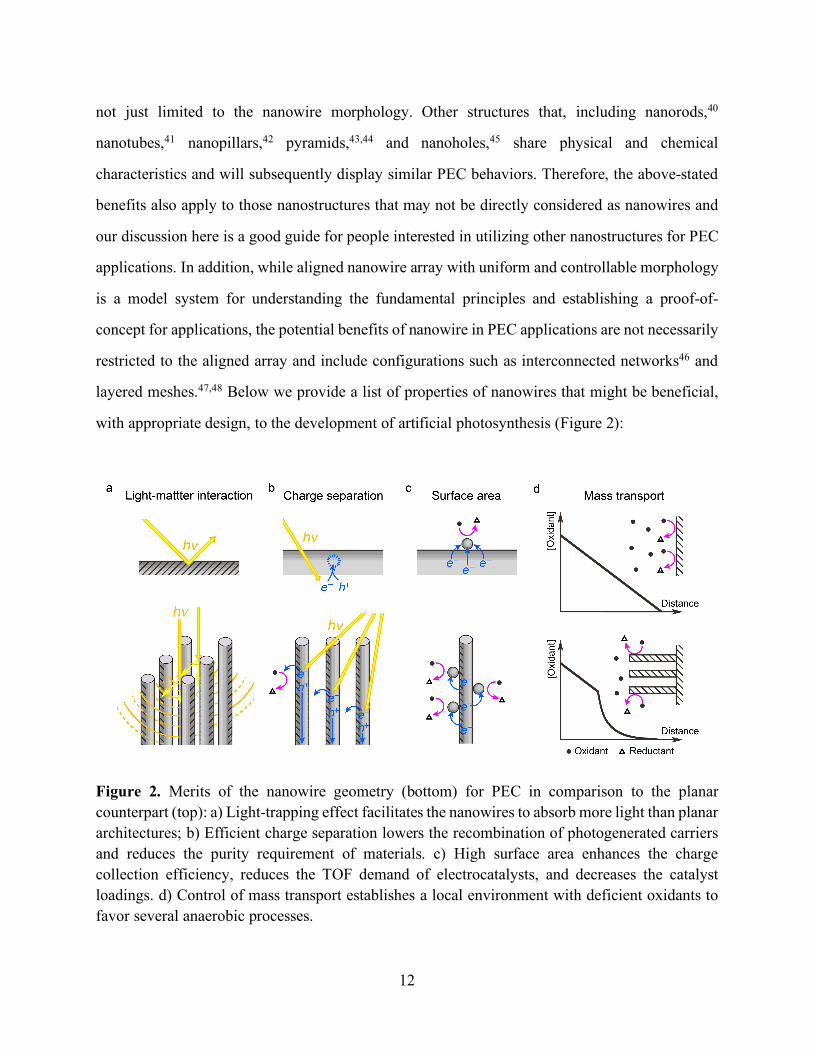
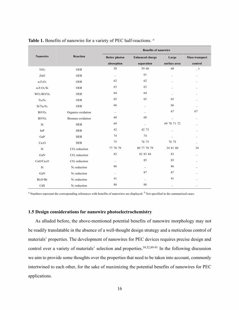
with appropriate design, to the development of artificial photosynthesis (Figure 2):
Figure 2. Merits of the nanowire geometry (bottom) for PEC in comparison to the planar counterpart (top): a) Light-trapping effect facilitates the nanowires to absorb more light than planar architectures; b) Efficient charge separation lowers the recombination of photogenerated carriers and reduces the purity requirement of materials. c) High surface area enhances the charge collection efficiency, reduces the TOF demand of electrocatalysts, and decreases the catalyst loadings. d) Control of mass transport establishes a local environment with deficient oxidants to favor several anaerobic processes.

13
Light-trapping for better photon absorption (Figure 2a). Nanowire, especially oriented
nanowire array, is a platform that provides a gradient of refractive index at the interface between
the liquid and semiconductors. This renders nanowire array remarkably suitable as an anti-
reflection layer,49,50 which suppresses reflection and enhances non-directional scattering of
incident light. Such a phenomenon, dubbed as the light-trapping effect, allows nanowire to exhibit
much higher equivalent absorption coefficients across a broad range of spectrum as compared to
a planar architecture of semiconductors. Additionally, for crystalline nanowires, the well-faceted
shape of the nanowire morphology creates unique optical modes that will further enhance the
absorption of incident photons at resonance wavelengths.51 Therefore, nanowire materials are
much better light-absorbers as compared to planar or bulk materials, thanks to their favorable
optical properties. Such a potential benefit will lower the cost of material preparation, especially
in the case of indirect semiconductors such as silicon (Si) that demands hundreds of micrometers
for appreciable absorption in the red part of the solar spectrum for a planar electrode.
Enhanced efficacy of charge separation (Figure 2b). Nanowire geometry can orthogonalize
the directionality of light absorption and the process of charge separation. In typical scenarios, the
incident photons are illuminated from an angle normal to the surface of semiconductor electrode
or material. For a bulk material or photoelectrode, this implies that photo-generated minority
carriers are required to travel the same distance as the equivalent absorption depth of the incident
photons. However, for many indirect semiconductor light-absorbers that are of interest to the
community, their minority carrier diffusion length and the width of band-bending region is much
shorter than absorption depth of the incident photons. This will lead to significant amount of
recombination of photo-excited carriers, a suboptimal value of ηseparation and subsequently lower
energy efficiencies. In contrast, nanowires allow the photogenerated minority carriers to travel a
much shorter distance to the materials/liquid interface, therefore significantly increase the value
of ηseparation.12,52 Such a decoupling between light absorption and charge separation on nanowire
materials is proposed to increase the overall quantum efficiency and energy efficiency of PEC
14
processes, at the same time may also increase the tolerance of impurities in the semiconductor
materials.
Increased reaction turnover thanks to its large surface area (Figure 2c). A redox half-reaction
at a sufficiently high rate of turnover is required at the semiconductor/electrolyte interface for an
efficient solar-to-chemical process. While different reactions may have their own intrinsic
reactivities, nanowire morphology provides a surface area that is much larger than its bulk or planar
counterparts, thereby offers more active sites for the solar-driven reactions. The high surface area
of nanowires will reduce the required overpotentials and flux density for the charge transfer of
half-reactions, therefore boost ηechem by outcompeting the possibility of surface-associated
recombination and increase the values of FF, Vonset, and the eventual energy efficiency.40,53 One
should note that such a contribution from nanowire morphology for PEC applications are
distinguishably different from the cases of PV studies, since large junction area in solar cells is
considered to reduce Voc by diluting the photon flux, as well as reduce FF by introducing more
surface recombination.52,54 Moreover, nanowire of large surface area is a suitable platform to
accommodate catalysts onto the semiconductor’s surface and deliver additional functionality to
the solar-to-chemical process. This is particularly beneficial for the use of earth-abundant building
blocks, as an increased loading amount of these building blocks can help to reduce the required
reactivity for the loaded catalysts and therefore help to achieve similar performance without the
use of precious metals.
Controlled mass transport within the nanowire array (Figure 2d). Nanowire array electrode
can be considered as a special form of porous electrodes, which has been intensively studied in the
past.55,56 One of the unique features of porous electrode is that the mass transport of redox species
within the electrode is highly predictable and tunable. With inappropriate design, such an issue of
mass transport can be a bane other than a blessing. Inadequate mass transport of redox-active
species for the proposed half-reaction requires additional free energy as driving force thereby
lowers the energy efficiency of a nanowire PEC device. However, we propose that the use of
nanowire array and its controllable mass transport can also be beneficial for some specific
15
applications when we aim to interface semiconductor light absorbers with functional building
blocks for artificial photosynthesis. One possible scenario is that the building block that the
nanowire is interfacing has a restrictive requirement about the local environment. Many
organometallic and microbial catalysts are highly sensitive to dioxygen (O2), yet a practical
application of artificial photosynthesis inevitably requires an oxygenic environment. It is
postulated that the nanowire array indeed can provide a local O2-free environment in air, thanks to
its control of mass transport for redox active species including O2.34,57 Such a property allows
nanowire arrays to embrace a broader range of building blocks and provide added flexibility when
designing an integrated system.
Benefits for device integration. The nanowire morphology is suitable to be integrated into a
functional device in the context of constructing a solar-powered chemical plant. Thanks to its large
aspect ratio and the mechanical flexibility, nanowires can be readily processed through a variety
of engineering techniques, including roll printing, drop casting and spin coating.14 The rapid
advance of synthetic methods for nanowires, especially low-temperature, solution-based
approaches, promise a scalable production of nanowire materials with affordable cost for large-
scale manufacturing, especially for the particulate configuration of photocatalysis. Moreover, as
we have mentioned above, the large surface area of the nanowire morphology also invites versatile
integration of nanowires with other building blocks in artificial photosynthesis. Here one specific
benefit of nanowires is its capability to mimic the microscopic structure and functionality of the
natural artificial photosynthetic system, which will be discussed in depth later in this review.
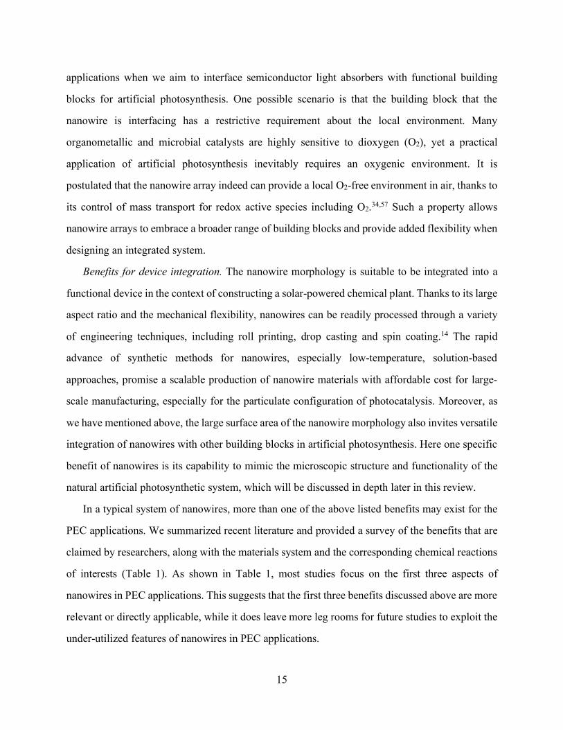
In a typical system of nanowires, more than one of the above listed benefits may exist for the
PEC applications. We summarized recent literature and provided a survey of the benefits that are
claimed by researchers, along with the materials system and the corresponding chemical reactions
of interests (Table 1). As shown in Table 1, most studies focus on the first three aspects of
nanowires in PEC applications. This suggests that the first three benefits discussed above are more
relevant or directly applicable, while it does leave more leg rooms for future studies to exploit the
under-utilized features of nanowires in PEC applications.
16
Table 1. Benefits of nanowire for a variety of PEC half-reactions. a
Nanowire Reaction
Benefits of nanowire
Better photon
absorption
Enhanced charge
separation
Large
surface area
Mass transport
control
TiO2 OER 58 59 60 60 – b
ZnO OER – 61 – –
α-F2O3 OER 62 62 – –
α-F2O3/Si OER 63 63 – –
WO3/BiVO4 OER 64 64 – –
Ta3N5 OER 65 65 65 –
Si/Ta3N5 OER 66 – 66 –
BiVO4 Organics oxidation – – 67 67
BiVO4 Biomass oxidation 68 68 – –
Si HER 69 – 69 70 71 72 –
InP HER 42 42 73 – –
GaP HER 74 74 – –
Cu2O HER 75 76 75 76 75 –
Si CO2 reduction 77 78 79 80 77 78 79 34 81 80 34
GaN CO2 reduction 82 82 83 84 83 –
CuO/Cu2O CO2 reduction – 85 85 –
Si N2 reduction 86 – 86 –
GaN N2 reduction – 87 87 –
Bi5O7Br N2 reduction 41 – 41 –
CdS N2 reduction 88 88 – –
a Numbers represent the corresponding references with benefits of nanowires are displayed. b Not specified in the summarized cases.
1.5 Design considerations for nanowire photoelectrochemistry
As alluded before, the above-mentioned potential benefits of nanowire morphology may not
be readily translatable in the absence of a well-thought design strategy and a meticulous control of
materials’ properties. The development of nanowires for PEC devices requires precise design and
control over a variety of materials’ selection and properties.39,52,89-91 In the following discussion
we aim to provide some thoughts over the properties that need to be taken into account, commonly
intertwined to each other, for the sake of maximizing the potential benefits of nanowires for PEC
applications.
17
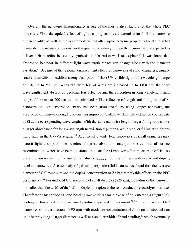
Overall, the nanowire dimensionality is one of the most critical factors for the whole PEC
processes. First, the optical effect of light-trapping requires a careful control of the nanowire
dimensionality as well as the accommodation of other optoelectronic properties for the targeted
materials. It is necessary to consider the specific wavelength range that nanowires are expected to
deliver their benefits, before any synthesis or fabrication work takes place.90 It was found that
absorption behavior in different light wavelength ranges can change along with the diameter
variation.92 Because of the resonant enhancement effect, Si nanowires of small diameters, usually
smaller than 200 nm, exhibits strong absorption of short UV-visible light in the wavelength range
of 300 nm to 500 nm. When the diameters of wires are increased up to 1400 nm, the short
wavelength light absorption becomes less effective and the absorption in long wavelength light
range of 500 nm to 900 nm will be enhanced.92 The influence of length and filling ratio of Si
nanowire on light absorption ability has been simulated.93 By using longer nanowire, the
absorption of long-wavelength photons was improved to alleviate the small extinction coefficients
of Si at the corresponding wavelengths. With the same nanowire length, larger filling ratio shows
a larger absorbance for long-wavelength near-infrared photons, while smaller filling ratio absorb
more light in the UV-Vis regime.93 Additionally, while long nanowires of small diameters may
benefit light absorption, the benefits of optical absorption may promote detrimental surface
recombination, which have been illustrated in detail for Si nanowires.90 Similar trade-off is also
present when we aim to maximize the value of ηseparation by fine-tuning the diameter and doping
level in nanowires. A case study of gallium phosphide (GaP) nanowires found that the average
diameter of GaP nanowire and the doping concentration of Zn had remarkable effects on the PEC
performance.91 For undoped GaP nanowire of small diameter (~25 nm), the radius of the nanowire
is smaller than the width of the built-in depletion region at the semiconductor/electrolyte interface.
Therefore the magnitude of band-bending was smaller than the case of bulk materials (Figure 3a),
leading to lower values of measured photovoltage and photocurrent.39,89 In comparison, GaP
nanowires of larger diameter (~90 nm) with moderate concentration of Zn dopant mitigated this
issue by providing a larger diameter as well as a smaller width of band bending,89 which eventually
18
yielded larger values of ηseparation and photocurrent density.89,91 However, excessively high
concentration of Zn dopant in GaP nanowires was detrimental, as the high concentration of dopants
increased recombination within the semicondcutor.91 Similar argument was observed for Si
nanowires.89 At a lower dopant density level (ND = 4.8 × 1015 cm‒3), photoelectrode of n-Si
nanowire showed a similar Voc but a lower light-saturated photocurrent density in comparison to
planar photoelectrode (Figure 3b). At a higher dopant density level (ND = 7.8 × 1017 cm‒3), the
light-saturated photocurrent density was higher for nanowire photoelectrode, but the Voc is smaller
than that of the planar photoelectrode (Figure 3b). In addition, the measured quantum yield was
also found to be strongly dependent on the properties of underlying Si substrate when the
penetration depths of incident photons could be longer than the length of Si nanowire.89 This
illustrates the importance of appropriate experimental design in order to extract fundamental
insights for nanowire-based photoelectrochemistry.
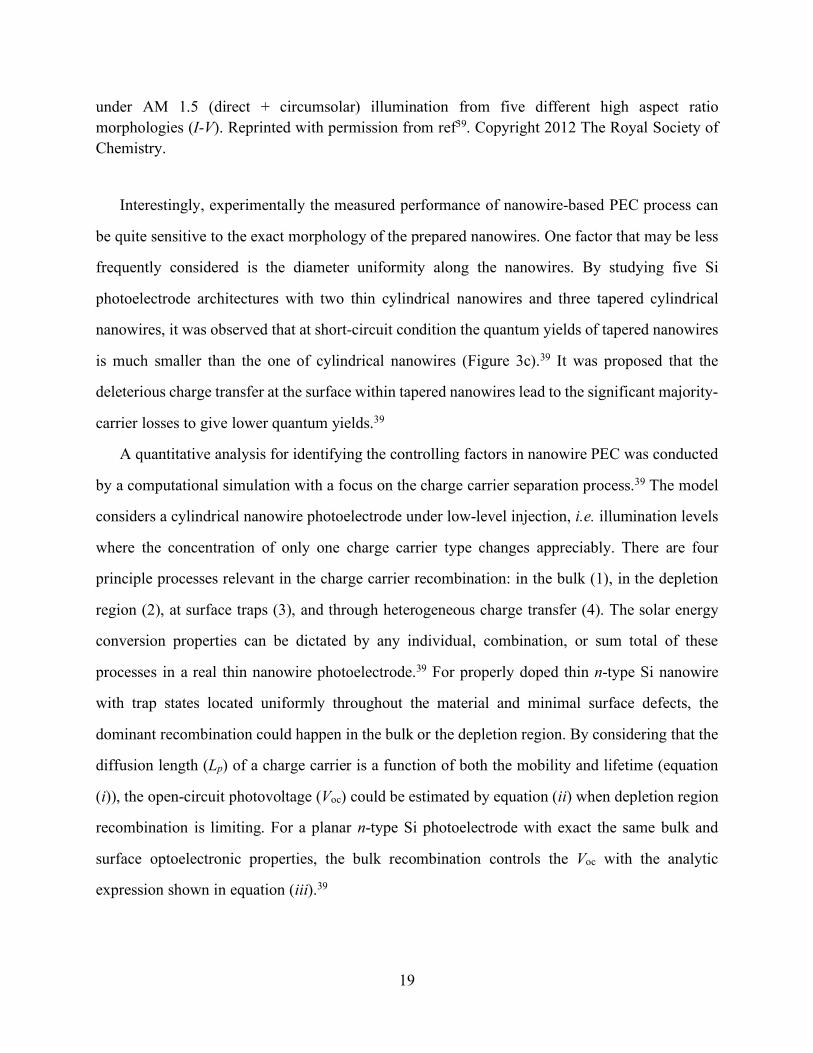
Figure 3. (a) Schematic illustration of the electrostatics of a GaP nanowire in electrolyte, exhibiting nanowire of small diameter suffers small band-bending, large diameter alleviates this issue, while it was not completely solved until Zn was introduced. Reprinted with permission from ref91. Copyright 2012 American Chemical Society. (b) Steady-state photocurrent-potential responses for planar and nanowire Si photoelectrodes: top) dopant density ND = 4.8 × 1015 cm‒3, and bottom) dopant density ND = 7.8 × 1017 cm‒3. Reprinted with permission from ref89. Copyright 2010 American Chemical Society. (c) Comparison of the simulated current-voltage photoresponse
19
under AM 1.5 (direct + circumsolar) illumination from five different high aspect ratio morphologies (I-V). Reprinted with permission from ref39. Copyright 2012 The Royal Society of Chemistry.
Interestingly, experimentally the measured performance of nanowire-based PEC process can
be quite sensitive to the exact morphology of the prepared nanowires. One factor that may be less
frequently considered is the diameter uniformity along the nanowires. By studying five Si
photoelectrode architectures with two thin cylindrical nanowires and three tapered cylindrical
nanowires, it was observed that at short-circuit condition the quantum yields of tapered nanowires
is much smaller than the one of cylindrical nanowires (Figure 3c).39 It was proposed that the
deleterious charge transfer at the surface within tapered nanowires lead to the significant majority-
carrier losses to give lower quantum yields.39
A quantitative analysis for identifying the controlling factors in nanowire PEC was conducted
by a computational simulation with a focus on the charge carrier separation process.39 The model
considers a cylindrical nanowire photoelectrode under low-level injection, i.e. illumination levels
where the concentration of only one charge carrier type changes appreciably. There are four
principle processes relevant in the charge carrier recombination: in the bulk (1), in the depletion
region (2), at surface traps (3), and through heterogeneous charge transfer (4). The solar energy
conversion properties can be dictated by any individual, combination, or sum total of these
processes in a real thin nanowire photoelectrode.39 For properly doped thin n-type Si nanowire
with trap states located uniformly throughout the material and minimal surface defects, the
dominant recombination could happen in the bulk or the depletion region. By considering that the
diffusion length (Lp) of a charge carrier is a function of both the mobility and lifetime (equation
(i)), the open-circuit photovoltage (Voc) could be estimated by equation (ii) when depletion region
recombination is limiting. For a planar n-type Si photoelectrode with exact the same bulk and
surface optoelectronic properties, the bulk recombination controls the Voc with the analytic
expression shown in equation (iii).39
20
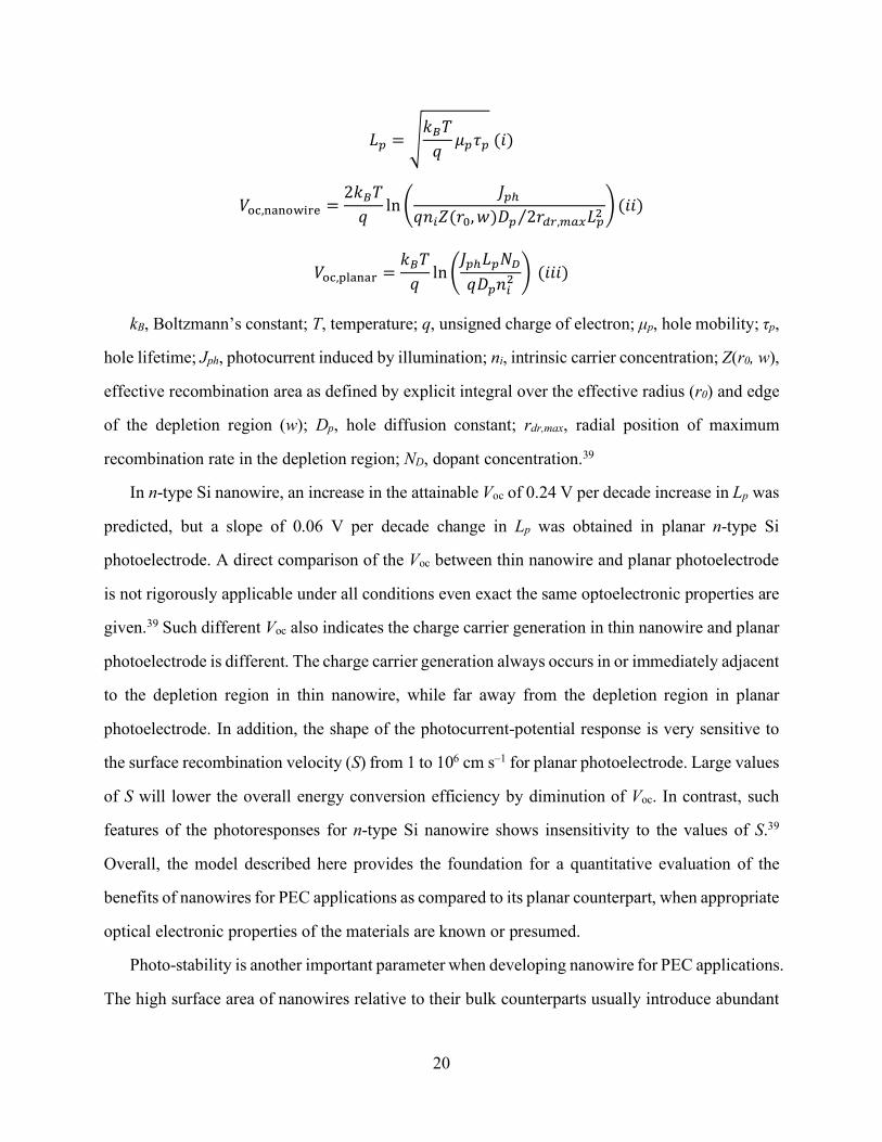
𝐿" = $𝑘&𝑇𝑞 𝜇"𝜏"(𝑖)
𝑉01,34305678 =2𝑘&𝑇𝑞 ln <
𝐽">𝑞𝑛@𝑍(𝑟C,𝑤)𝐷" 2𝑟FG,HIJ𝐿"K⁄ M (𝑖𝑖)
𝑉01,NO4347 =𝑘&𝑇𝑞 ln <
𝐽">𝐿"𝑁Q𝑞𝐷"𝑛@K
M(𝑖𝑖𝑖)
kB, Boltzmann’s constant; T, temperature; q, unsigned charge of electron; µp, hole mobility; τp,
hole lifetime; Jph, photocurrent induced by illumination; ni, intrinsic carrier concentration; Z(r0, w),
effective recombination area as defined by explicit integral over the effective radius (r0) and edge
of the depletion region (w); Dp, hole diffusion constant; rdr,max, radial position of maximum
recombination rate in the depletion region; ND, dopant concentration.39
In n-type Si nanowire, an increase in the attainable Voc of 0.24 V per decade increase in Lp was
predicted, but a slope of 0.06 V per decade change in Lp was obtained in planar n-type Si
photoelectrode. A direct comparison of the Voc between thin nanowire and planar photoelectrode
is not rigorously applicable under all conditions even exact the same optoelectronic properties are
given.39 Such different Voc also indicates the charge carrier generation in thin nanowire and planar
photoelectrode is different. The charge carrier generation always occurs in or immediately adjacent
to the depletion region in thin nanowire, while far away from the depletion region in planar
photoelectrode. In addition, the shape of the photocurrent-potential response is very sensitive to
the surface recombination velocity (S) from 1 to 106 cm s–1 for planar photoelectrode. Large values
of S will lower the overall energy conversion efficiency by diminution of Voc. In contrast, such
features of the photoresponses for n-type Si nanowire shows insensitivity to the values of S.39
Overall, the model described here provides the foundation for a quantitative evaluation of the
benefits of nanowires for PEC applications as compared to its planar counterpart, when appropriate
optical electronic properties of the materials are known or presumed.
Photo-stability is another important parameter when developing nanowire for PEC applications.
The high surface area of nanowires relative to their bulk counterparts usually introduce abundant
21
surface defects as carrier trapping centers. This could lead to the pinning of surface Fermi level
and a resultant band bending with a reduced photovoltage and subsequently reduced PEC
efficiency.94-96 These uncontrolled surface processes can also induce photocorrosion, a decrease
of electric conductivity, and degradation of nanowire materials.96 Coupling catalysts with
nanowires will facilitate the charge transfer and a timely consumption of photo-generated carriers
to help improve the photo-stability, as will be discussed in section 2.3. The passivation of the
nanowire surface is another effective method to boost device efficiency and stability.70,96-103 In the
case of Si and III-V semiconductor materials, thin-film of amorphous oxide such as TiO2 are very
successful in impeding the surface corrosion while allowing the passage of high densities of
photocurrents.70,98,99,101,103 These oxide layers are also reported to increase the adhesion of the
deposited metal catalysts and prevent aggregation on Si’s surface.98 Additionally, treating
electrode surface with 1,2-ethanedithiol is reported to improve the separation and lifetimes of
photo-excited charge carriers thanks to the suppression of surface oxygen-containing dangling
bonds.96 Advanced strategies to expand the scope of surface passivation for a broader range of
semiconductor nanowires will definitely benefit the application of nanowires in PEC applications.
In general, the nanowire morphology does not automatically guarantee a better PEC
performance as compared to its bulk counterparts, nor it means that we can neglect the intrinsic
properties of the semiconductor materials that were utilized. In order to optimize a nanowire PEC
device, the three important efficiencies discussed in section 1.3, ηoptical, ηseparation and ηechem, must
be considered and a suitable design strategy should be applied. In the rest of this review, we
examine the current literature and provide additional thoughts towards an effective PEC device of
nanowires.
2. Functionalized semiconductor nanowires for photoelectrochemistry
2.1 A survey of building blocks in photoelectrochemistry
To maximize the overall solar-to-energy efficiency, each step in the PEC process, including
the light absorption, charge separation and transportation, and electrochemical reaction, should be
22
optimized.12,39,104 A semiconductor alone usually may not possess the suitable properties for all of
these steps, which calls for the integration of other building blocks in artificial photosynthesis with
the use of nanowire morphology.12,52,89 One type of the building blocks that may be needed is
additional light-absorbers, often dubbed as light co-absorbers or photosensitizers, which can
maximize the absorption of incident photons (Figure 4a). Wide band-gap semiconductors such as
TiO2 only absorb ultraviolet light that is only 4% of the solar spectrum, which is not sufficient for
high energy efficiency.105,106 For semiconductors of indirect band-gaps such as hematite Fe2O3,
the nature of their low absorption coefficients posts as a major challenge for higher
efficiency.105,106 The introduction of co-absorbers will help to address the challenges mentioned
above. Another type of useful building blocks are catalytic species, termed as catalysts, that will
accelerate the charge transfer at the interface between semiconductors and electrolyte (Figure 4b).
An efficient PEC device relies on the efficient charge transfer of the accumulated minority carriers
without significant recombination.39 Yet many of half-reactions that are of interest to artificial
photosynthesis, such as water splitting or the reduction of CO2, are multi-electron multi-proton
reactions whose intrinsic reactivity may not high on the semiconductors’ surface. This requires the
deposition of catalysts on the semiconductors’ surface to lower the kinetic barrier of
electrochemical reactions and maintain a large value of ηechem leading to lower the efficiency of
charge separation and transport to the semiconductor/electrolyte interface (ηseparation).107 The
following sessions describe the advances in the integration of nanowires with both light-absorbers
and catalysts. To assist the discussion, we provide a few tables that summarize some recent
advances (Tables 2 to 5). In these tables, we not only provide the information associated with the
semiconductor nanowires and loaded co-absorbers and catalysts, but also list the chemical
reactions that are involved and their corresponding PEC performances.
23
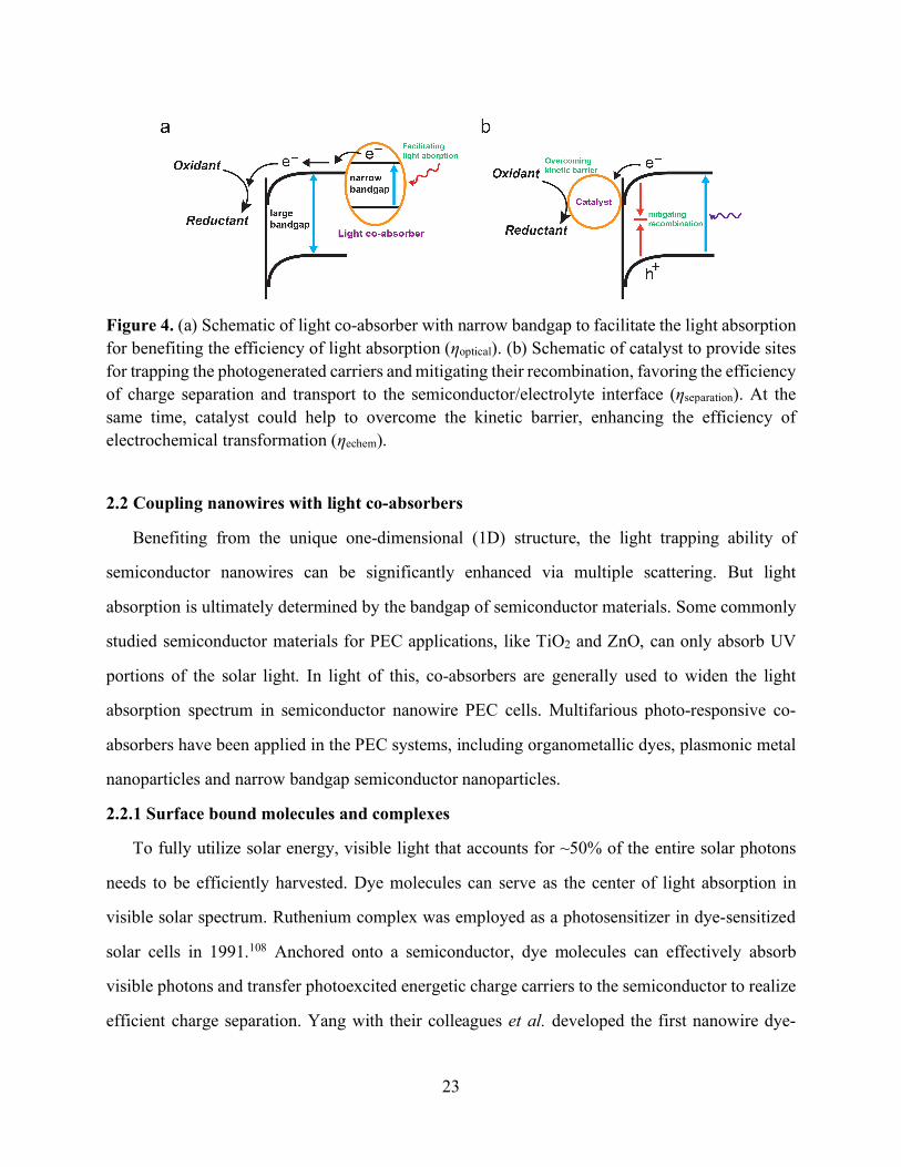
Figure 4. (a) Schematic of light co-absorber with narrow bandgap to facilitate the light absorption for benefiting the efficiency of light absorption (ηoptical). (b) Schematic of catalyst to provide sites for trapping the photogenerated carriers and mitigating their recombination, favoring the efficiency of charge separation and transport to the semiconductor/electrolyte interface (ηseparation). At the same time, catalyst could help to overcome the kinetic barrier, enhancing the efficiency of electrochemical transformation (ηechem).
2.2 Coupling nanowires with light co-absorbers
Benefiting from the unique one-dimensional (1D) structure, the light trapping ability of
semiconductor nanowires can be significantly enhanced via multiple scattering. But light
absorption is ultimately determined by the bandgap of semiconductor materials. Some commonly
studied semiconductor materials for PEC applications, like TiO2 and ZnO, can only absorb UV
portions of the solar light. In light of this, co-absorbers are generally used to widen the light
absorption spectrum in semiconductor nanowire PEC cells. Multifarious photo-responsive co-
absorbers have been applied in the PEC systems, including organometallic dyes, plasmonic metal
nanoparticles and narrow bandgap semiconductor nanoparticles.
2.2.1 Surface bound molecules and complexes
To fully utilize solar energy, visible light that accounts for ~50% of the entire solar photons
needs to be efficiently harvested. Dye molecules can serve as the center of light absorption in
visible solar spectrum. Ruthenium complex was employed as a photosensitizer in dye-sensitized
solar cells in 1991.108 Anchored onto a semiconductor, dye molecules can effectively absorb
visible photons and transfer photoexcited energetic charge carriers to the semiconductor to realize
efficient charge separation. Yang with their colleagues et al. developed the first nanowire dye-
24
sensitized solar cell, which not only offers fast electron transport, but also can improve quantum
efficiency in the red region of the solar spectrum.20 Dye-sensitized configuration has been recently
applied in photoelectrochemical catalysis.109-113 There are four main components in a dye-
sensitized photoelectrochemical catalysis system, i.e. visible light absorbing sensitizer, oxidation
catalyst, reduction catalyst, and semiconductor electrode. Visible-light absorbing dye molecules
can be adsorbed onto surface of semiconductor and facilitate separation of photogenerated carriers
to drive catalytic reactions.111 Efficient light absorption by sensitizers requires electrode with large
surface area. Table 2 summarizes the surface-bonding dye molecules as light co-absorbers in
nanowire photoelectrochemical systems, for example InGaN nanowire photoelectrode could
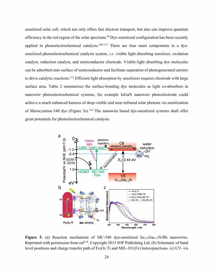
achieve a much enhanced harness of deep-visible and near-infrared solar photons via sensitization
of Merocyanine-540 dye (Figure 5a).114 The nanowire based dye-sensitized systems shall offer
great potentials for photoelectrochemical catalysis.
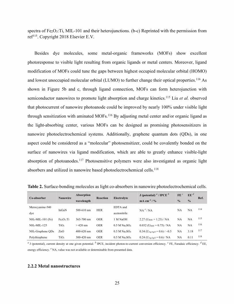
Figure 5. (a) Reaction mechanism of MC-540 dye-sensitized In0.25Ga0.75N/Rh nanowires. Reprinted with permission from ref114. Copyright 2015 IOP Publishing Ltd. (b) Schematic of band level positions and charge transfer path of Fe2O3:Ti and MIL-101(Fe) heterojunctions. (c) UV–vis
25
spectra of Fe2O3:Ti, MIL-101 and their heterojunctions. (b-c) Reprinted with the permission from ref115. Copyright 2018 Elsevier E.V.
Besides dye molecules, some metal-organic frameworks (MOFs) show excellent
photoresponse to visible light resulting from organic ligands or metal centers. Moreover, ligand
modification of MOFs could tune the gaps between highest occupied molecular orbital (HOMO)
and lowest unoccupied molecular orbital (LUMO) to further change their optical properties.116 As
shown in Figure 5b and c, through ligand connection, MOFs can form heterojunction with
semiconductor nanowires to promote light absorption and charge kinetics.115 Liu et al. observed
that photocurrent of nanowire photoanode could be improved by nearly 100% under visible light
through sensitization with aminated MOFs.116 By adjusting metal center and/or organic ligand as
the light-absorbing center, various MOFs can be designed as promising photosensitizers in
nanowire photoelectrochemical systems. Additionally, graphene quantum dots (QDs), in one
aspect could be considered as a “molecular” photosensitizer, could be covalently bonded on the
surface of nanowires via ligand modification, which are able to greatly enhance visible-light
absorption of photoanodes.117 Photosensitive polymers were also investigated as organic light
absorbers and utilized in nanowire based photoelectrochemical cells.118
Table 2. Surface-bonding molecules as light co-absorbers in nanowire photoelectrochemical cells.
Co-absorber Nanowire Absorption
wavelength Reaction Electrolyte
J (potential) a / IPCE b
mA cm‒2 / %
FE c
%
EE d
% Ref.
Merocyanine-540
dye InGaN 500-610 nm HER
EDTA and
acetonitrile NA e / NA NA NA 114
NH2-MIL-101 (Fe) Fe2O3:Ti 365-700 nm OER 1 M NaOH 2.27 (URHE = 1.23) / NA NA NA 115 NH2-MIL-125 TiO2 > 420 nm OER 0.5 M Na2SO4 0.032 (URHE = 0.75) / NA NA NA 116 NH2-Graphene QDs ZnO 400-620 nm OER 0.5 M Na2SO4 0.34 (UAg/AgCl = 0.6) / ~0.5 NA 3.18 117 Polythiophene TiO2 300-420 nm OER 0.5 M Na2SO4 0.24 (UAg/AgCl = 0.6) / NA NA 0.11 118
a J (potential), current density at one given potential. b IPCE, incident photon-to-current conversion efficiency. c FE, Faradaic efficiency. d EE,
energy efficiency. e NA, value was not available or determinable from presented data.
2.2.2 Metal nanostructures
26
Plasmonic metal nanostructures show distinctive light absorption properties resulting from
localized surface plasmon resonance effect. When incident photon frequency matches with the
inherent frequency of collective oscillation of free electrons (on the surface of metal nanostructures)
against the restoring force of positive nuclei, surface plasmon resonance is created,119 which will
give rise to intensive and highly localized electromagnetic field in metal nanostructures,
manifesting as greatly enhanced light absorption at specific wavelength as shown in Figure 6a.
The resonant wavelength and intensity are dependent on the nature of metal, together with the size
and shape of the metal nanostructures. By manipulating composition, shape and size of plasmonic
nanostructures, the plasmonic bands can be tuned from visible to near-IR region and thus it is
possible to design multiple metallic nanostructures serving as light absorbers to harvest solar
photons.119 It has been demonstrated that Ag and Au nanoparticles can significantly improve light
absorption and charge kinetics via plasmonic effect in nanowire PEC cells.120-122 Following light
absorption, electrons from the occupied states are stimulated above the Fermi level to transform
into hot-electrons, which with adequate and suitable energies can be utilized for catalysis. Rapid
hot-electron separation before charge recombination is the key to achieve high energy conversion
efficiency.123,124 Hot-electrons can be injected into semiconductors following a similar mechanism
as dye sensitization. When attached to a semiconductor photoelectrode, plasmonic metal
nanostructures absorb resonant photons and deliver the photo-excited electrons to the neighboring
semiconductor for an increased optical response in a wide spectral range. Table 3 summarizes the
metal nanostructures used as light-absorbers to improve light absorption in nanowire-based PEC
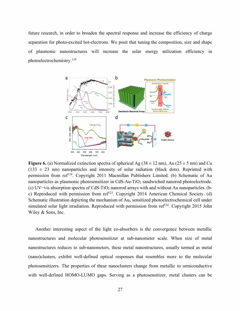
systems. For example, in CdS-Au-TiO2 sandwiched nanorod photoelectrode, Au nanoparticles act
as the plasmonic photosensitizer to extend light absorption from visible to near-infrared (Figure
6b-c).122 A roughly 30-time enhancement of reaction rate for water oxidation could be obtained
after 1.0 wt% Au nanoparticles decorated on BiFeO3 nanowires suspension system.125 Despite
such promising properties, current research has only witness a limited numbers of metallic
plasmonic nanostructures used in PEC systems, with limited variations in composition, size and
shape of the metallic nanostructures. This should be one of the aspects that should be addressed in
27
future research, in order to broaden the spectral response and increase the efficiency of charge
separation for photo-excited hot-electrons. We posit that tuning the composition, size and shape
of plasmonic nanostructures will increase the solar energy utilization efficiency in
photoelectrochemistry.119
Figure 6. (a) Normalized extinction spectra of spherical Ag (38 ± 12 nm), Au (25 ± 5 nm) and Cu (133 ± 23 nm) nanoparticles and intensity of solar radiation (black dots). Reprinted with permission from ref119. Copyright 2011 Macmillan Publishers Limited. (b) Schematic of Au nanoparticles as plasmonic photosensitizer in CdS-Au-TiO2 sandwiched nanorod photoelectrode. (c) UV−vis absorption spectra of CdS-TiO2 nanorod arrays with and without Au nanoparticles. (b-c) Reproduced with permission from ref122. Copyright 2014 American Chemical Society. (d) Schematic illustration depicting the mechanism of Aux sensitized photoelectrochemical cell under simulated solar light irradiation. Reproduced with permission from ref126. Copyright 2015 John Wiley & Sons, Inc.
Another interesting aspect of the light co-absorbers is the convergence between metallic
nanostructures and molecular photosensitizer at sub-nanometer scale. When size of metal
nanostructures reduces to sub-nanometers, these metal nanostructures, usually termed as metal
(nano)clusters, exhibit well-defined optical responses that resembles more to the molecular
photosensitizers. The properties of these nanoclusters change from metallic to semiconductive
with well-defined HOMO-LUMO gaps. Serving as a photosensitizer, metal clusters can be
28
photoexcited under visible light illumination and thus generate electron-hole pairs. Liu et al.
demonstrated that photogenerated electrons from Aux clusters could be readily injected into the
conduction band of TiO2 to realize efficient charge separation (Figure 6d).126 Metal nanocluster
sensitization has already been applied in nanowire-based photoelectrochemical systems.127
Table 3. Metallic nanostructures as light co-absorbers in nanowire-based photoelectrochemical cells.
Co-absorber Nanowire Absorption
wavelength Reaction Electrolyte
J (potential) a / IPCE b
mA cm‒2 / %
FE c
%
EE d
% Ref.
Au nanoparticles ZnO > 420 nm OER 0.5 M Na2SO4 0.3 (UAg/AgCl = 1.0) / NA e 69 NA 120 Ag@Ag3(PO4)1-x
nanoparticles ZnO 300-590 nm OER 0.5 M Na2SO4 3.1 (UPt = 0.6) / 60 NA 2 121
Au nanohole
array α-Fe2O3 300-675 nm OER 1 M NaOH ~0.95 (UAg/AgCl = 0.23) / 17.4 NA NA 62
Au nanoparticles/
Au nanorods TiO2 300-800 nm OER 1 M NaOH NA / ~0.014 NA NA 128
Au nanoparticles Si@α-Fe2O3 350-1100 nm OER 1 M NaOH /
Na3PO4 2.60 (UPt = 0) / 12 NA 6 129
Ag nanoparticles ZnO 400-800 nm OER 0.5 M Na2SO4 1.8 (UAg/AgCl = 0) / 3.9 NA NA 130
Au interlayer CdS 400-625 nm Water
splitting
0.2 M Na2S/1 M
Na2SO3 10.5 (UAg/AgCl = 0) / ~30 NA NA 131
Au@CdS
nanoparticles TiO2 525-725 nm
Water
splitting
0.35 M Na2SO3 /
0.25 M Na2S 4.07 (UAg/AgCl = 0) / 85 NA 2.8 122
Ag@Ag2S
nanoparticles Ti@TiO2 300-650 nm
Water
splitting 1 M NaOH 0.089 (UPt = 0.2) / NA NA NA 132
Au nanoparticles 3D ZnO 300-750 nm OER 0.5 M Na2SO4 4.07 (URHE = 1) / ~5.5 NA 0.52 133
Ag nanoparticles Si@PEDOT 350-875 nm Water
splitting
pH=1, H2SO4+
water /methanol 6.6 (USCE = 0) / 40 NA 2.86 134
Au@SiO2
nanoparticles Cu2O 400-600 nm HER 0.1 M Na2SO4 ‒29 (URHE = 0) / ~0.45 NA NA 135
Aux nanoclusters TiO2 200-600 nm OER 0.1 M Na2S ~0.15 (UAg/AgCl = 0) / NA NA NA 126
Au nanoparticles ZnO/ZnS
core-shell NA OER 0.5 M Na2SO4 0.58 (UAg/AgCl = 1) / NA NA 0.21 136
Au3Cu
nanoparticles Silicon NA
CO2
reduction 0.1 M KHCO3 2.2 (URHE = ‒0.2) / NA 80 NA 81
Cu nanoparticles GaN NA CO2
reduction 0.5 M KHCO3 44.9 (UAg/AgCl = ‒1.5) / NA 19 NA 137
29
a J (potential), current density at one given potential. b IPCE, incident photon-to-current conversion efficiency. c FE, Faradaic efficiency. d EE,
energy efficiency. e NA, value was not available or determinable from presented data.
2.2.3 Semiconductor nanoparticles
Semiconductor-semiconductor junction offers another class of hybrid structures to enhance
light absorption. Since the discovery of photosensitization effect in TiO2 electrode during water
electrolysis, the research of hybrid semiconductor systems for photo(electro)catalysis has made
tremendous progresses.38,146,147 In order to remedy the limited light absorption of single
semiconductor material in photoelectrochemistry, semiconductor heterojunctions are constructed.
Semiconductor-semiconductor junctions can be used to extend the light absorption range and at
the same time improve the efficacy of electron-hole separation for the photo-generated carriers.148
In virtue of the high aspect ratio of nanowires, semiconductor nanoparticles can be easily deposited
on the surface of nanowires. Owing to their differences in the flat-band potentials and band
structures, a variety of models for the band alignments with different terminologies, such as
semiconductor sensitization, Type II, phase junction, and Z-scheme, can be established when
semiconductor nanoparticles are interfaced with semiconductor nanowires.148 If both
semiconductor components are photo-excitable, semiconductor nanoparticles with suitable energy
band can form favorable band alignments with the nanowires. Such a configuration can effectively
broaden the spectral response of light absorption and promote charge separation. One example that
Ag nanoparticles ZnO/CdS
core-shell 375-550 nm OER
0.25 M Na2S /
0.35 M Na2SO3 ~4 (USCE = 0) / ~22 NA 3.13 138
Au nanoparticles ZnO/Al2O3
core-shell NA OER 0.5 M Na2SO4 0.512 (UAg/AgCl = 1) / NA NA 0.67 139
Au nanoparticles 3D TiO2 400-700 nm OER 1 M NaOH 2.69 (USCE = 0) / NA NA NA 140 Aux nanoclusters ZnO 300-450 nm OER 0.5 M Na2SO4 ~0.8 (URHE = 1.2) / NA NA NA 127
Au nanoparticles BiVO4/ZnO 400-550 nm OER pH=7.2, 0.5 M
PBS 2.87 (URHE = 1.23) / 40 NA NA 141
Au nanostars TiO2 400-800 nm OER 1 M NaOH 0.95 (UNHE = 1) / 0.4 NA NA 142 Ni nanoparticles H-TiO2 300-500 nm OER 1 M KOH 0.165 (UAg/AgCl = 0.23) / 7.5 NA NA 143 Ag nanoparticles NaNbO3 NA OER 0.5 M NaOH 3.54 (UAg/AgCl = 0.9) / NA NA NA 144 Au@SiO2
nanoparticles α-Fe2O3 NA OER 0.5 M Na2SO4 ~0.1 (URHE = 0.8) / ~0.03 NA NA 145
30
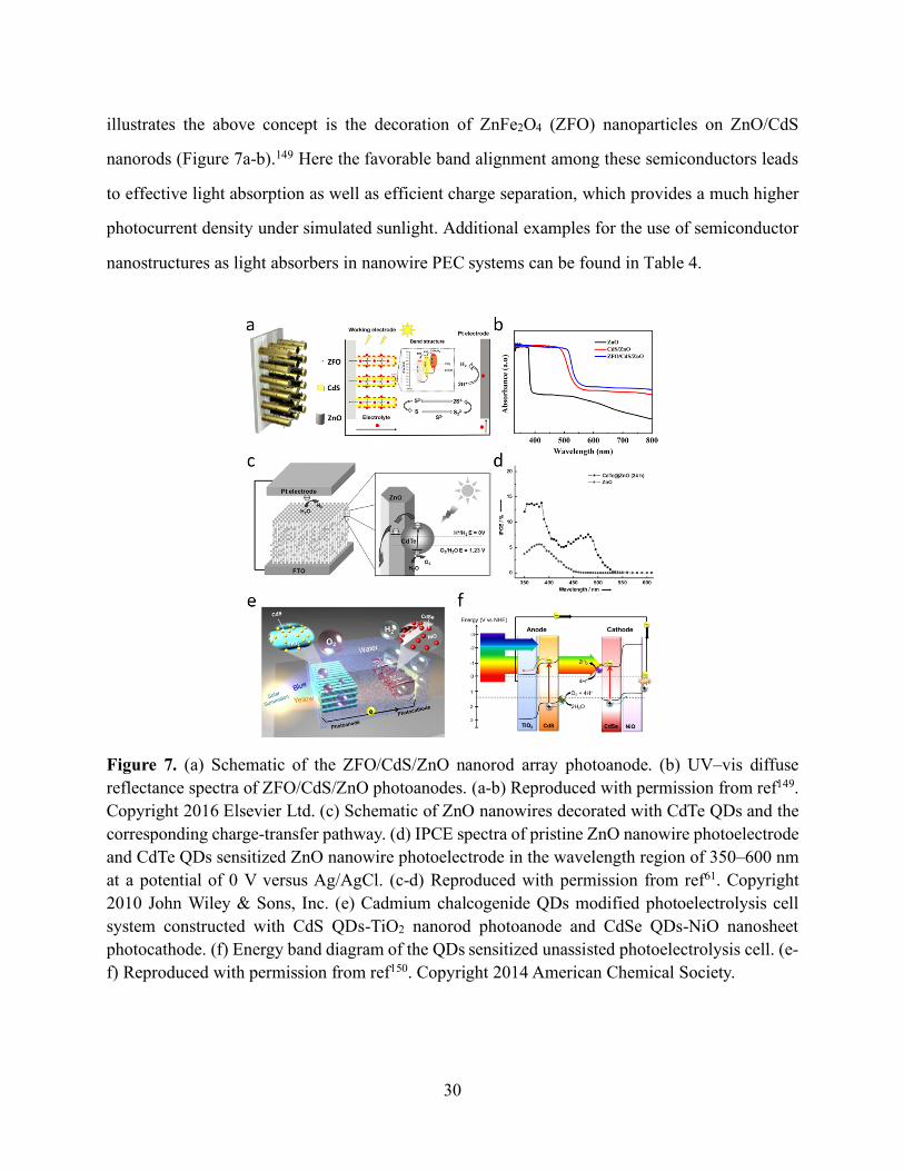
illustrates the above concept is the decoration of ZnFe2O4 (ZFO) nanoparticles on ZnO/CdS
nanorods (Figure 7a-b).149 Here the favorable band alignment among these semiconductors leads
to effective light absorption as well as efficient charge separation, which provides a much higher
photocurrent density under simulated sunlight. Additional examples for the use of semiconductor
nanostructures as light absorbers in nanowire PEC systems can be found in Table 4.
Figure 7. (a) Schematic of the ZFO/CdS/ZnO nanorod array photoanode. (b) UV–vis diffuse reflectance spectra of ZFO/CdS/ZnO photoanodes. (a-b) Reproduced with permission from ref149. Copyright 2016 Elsevier Ltd. (c) Schematic of ZnO nanowires decorated with CdTe QDs and the corresponding charge-transfer pathway. (d) IPCE spectra of pristine ZnO nanowire photoelectrode and CdTe QDs sensitized ZnO nanowire photoelectrode in the wavelength region of 350–600 nm at a potential of 0 V versus Ag/AgCl. (c-d) Reproduced with permission from ref61. Copyright 2010 John Wiley & Sons, Inc. (e) Cadmium chalcogenide QDs modified photoelectrolysis cell system constructed with CdS QDs-TiO2 nanorod photoanode and CdSe QDs-NiO nanosheet photocathode. (f) Energy band diagram of the QDs sensitized unassisted photoelectrolysis cell. (e-f) Reproduced with permission from ref150. Copyright 2014 American Chemical Society.
31
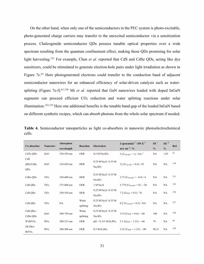
On the other hand, when only one of the semiconductors in the PEC system is photo-excitable,
photo-generated charge carriers may transfer to the unexcited semiconductor via a sensitization
process. Chalcogenide semiconductor QDs possess tunable optical properties over a wide
spectrum resulting from the quantum confinement effect, making these QDs promising for solar
light harvesting.151 For example, Chen et al. reported that CdS and CdSe QDs, acting like dye
sensitizers, could be stimulated to generate electron-hole pairs under light irradiation as shown in
Figure 7c.61 Here photogenerated electrons could transfer to the conduction band of adjacent
semiconductor nanowires for an enhanced efficiency of solar-driven catalysis such as water-
splitting (Figure 7e-f).61,150 Mi et al. reported that GaN nanowires loaded with doped InGaN
segments can proceed efficient CO2 reduction and water splitting reactions under solar
illumination.152,153 Here one additional benefits is the tunable band-gap of the loaded InGaN based
on different synthetic recipes, which can absorb photons from the whole solar spectrum if needed.
Table 4. Semiconductor nanoparticles as light co-absorbers in nanowire photoelectrochemical cells.
Co-absorber Nanowire Absorption
wavelength Reaction Electrolyte
J (potential) a / IPCE b
mA cm‒2 / %
FE c
%
EE d
% Ref.
CdTe QDs ZnO 350-550 nm OER 0.5 M Na2SO4 2 (UAg/AgCl = 1) / NA e NA 1.83 61 CdS
QDs/CdSe
QDs
ZnO 310-650 nm HER 0.25 M Na2S / 0.35 M
Na2SO3 12 (UAg/AgCl = 0.4) / 45 NA NA 154
CdSe QDs TiO2 350-600 nm HER 0.25 M Na2S / 0.35 M
Na2SO3 2.75 (UAg/AgCl = ‒0.4) / 6 NA NA 151
CdS QDs TiO2 375-600 nm OER 1 M Na2S 5.778 (UAg/AgCl = 0) / ~20 NA NA 155
CdS QDs TiO2 350-550 nm HER 0.25 M Na2S / 0.35 M
Na2SO3 7.2 (URHE = 0.5) / 76 NA NA 156
CdS QDs TiO2 NA Water
splitting
0.25 M Na2S / 0.35 M
Na2SO3 0.2 (UAg/AgCl = 0.5) / NA NA NA 157
CdS QDs /
CdSe QDs ZnO 300-750 nm
Water
splitting
0.25 M Na2S / 0.35 M
Na2SO3 13.9 (URHE = 0.6) / ~80 100 NA 158
W:BiVO4 WO3 300-515 nm OER pH = 8, 0.5 M K3PO4 3.1 (URHE = 1.23) / ~60 79 NA 64 (W,Mo)-
BiVO4 WO3 300-500 nm OER 0.5 M K2SO4 5.35 (URHE = 1.23) / ~90 96.21 NA 159
32
a J (potential), current density at one given potential. b IPCE, incident photon-to-current conversion efficiency. c FE, Faradaic efficiency. d EE,
energy efficiency. e NA, value was not available or determinable from presented data.
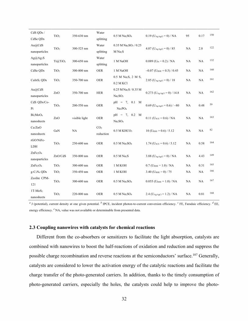
2.3 Coupling nanowires with catalysts for chemical reactions
Different from the co-absorbers or sensitizers to facilitate the light absorption, catalysts are
combined with nanowires to boost the half-reactions of oxidation and reduction and suppress the
possible charge recombination and reverse reactions at the semiconductors’ surface.107 Generally,
catalysts are considered to lower the activation energy of the catalytic reactions and facilitate the
charge transfer of the photo-generated carriers. In addition, thanks to the timely consumption of
photo-generated carriers, especially the holes, the catalysts could help to improve the photo-
CdS QDs /
CdSe QDs TiO2 350-630 nm
Water
splitting 0.5 M Na2SO4 0.19 (UAg/AgCl = 0) / NA 95 0.17 150
Au@CdS
nanoparticles TiO2 300-525 nm
Water
splitting
0.35 M Na2SO3 / 0.25
M Na2S 4.07 (UAg/AgCl = 0) / 85 NA 2.8 122
Ag@Ag2S
nanoparticles Ti@TiO2 300-650 nm
Water
splitting 1 M NaOH 0.089 (UPt = 0.2) / NA NA NA 132
CdSe QDs TiO2 300-800 nm OER 1 M NaOH ~0.07 (URHE = 0.5) / 0.45 NA NA 160
CuInS2 QDs TiO2 350-700 nm OER 0.5 M Na2S, 2 M S,
0.2 M KCl 2.85 (UAg/AgCl = 0) / 18 NA NA 161
Au@CdS
nanoparticles ZnO 350-700 nm HER
0.25 M Na2S / 0.35 M
Na2SO3 0.273 (UAg/AgCl = 0) / 14.8 NA NA 162
CdS QDs/Co-
Pi TiO2 200-550 nm OER
pH = 7, 0.1 M
Na3PO4 0.69 (UAg/AgCl = 0.6) / ~80 NA 0.48 59
Bi2MoO6
nanosheets ZnO visible light OER
pH = 7, 0.2 M
Na2SO4 0.11 (USCE = 0.6) / NA NA NA 163
Cu/ZnO
nanosheets GaN NA
CO2
reduction 0.5 M KHCO3 10 (URHE = 0.6) / 5.12 NA NA 82
rGO/NiFe-
LDH TiO2 250-600 nm OER 0.5 M Na2SO4 1.74 (USCE = 0.6) / 5.12 NA 0.58 164
ZnFe2O4
nanoparticles ZnO/CdS 350-800 nm OER 0.5 M Na2S 3.88 (UAg/AgCl = 0) / NA NA 4.43 149
ZnFe2O4 TiO2 300-600 nm OER 1 M KOH 0.7 (URHE = 1.0) / NA NA 0.31 165 g-C3N4 QDs TiO2 350-450 nm OER 1 M KOH 3.40 (URHE = 0) / 75 NA NA 166 Zeolite CPM-
121 TiO2 300-600 nm OER 0.5 M Na2SO4 0.055 (URHE = 1.0) / NA NA NA 167
1T-MoS2
nanosheets TiO2 220-800 nm OER 0.5 M Na2SO4 2.4 (UAg/AgCl = 1.2) / NA NA 0.81 168
33
stability of nanowires if that is an issue.107 The catalysts are usually classified into three categories:
molecular/cluster catalysts, inorganic materials, and biological entities (Table 5).
2.3.1 Molecular/cluster as catalysts
The molecular/cluster catalysts with earth-abundant elements always possess the advantages
of definite and designable structures, tunable redox properties, and potential links to material
surface,169 rendering them suitable as catalysts for nanowires.80,87,170-174 However, as these
catalysts seem to be less stable under oxidative environment,169 they are more often applied to
photocathode rather than photoanode. At the photocathode, Si is the most popular semiconductor
material that has so far been studied, thanks to its low band-gap (1.1 eV), high carrier mobility,
long life-time of photo-excited carriers, and commercial availability.9 One of the most common
applications for Si nanowires as a photocathode is solar-powered proton reduction into
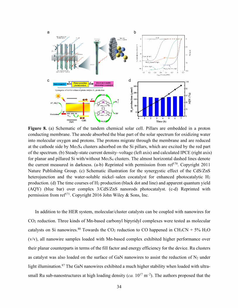
dihydrogen.9 An incomplete cubane-like Mo3S4 cluster has been coupled with Si nanopillar as
photocathode to catalyze the hydrogen evolution reaction (HER) (Figure 8a-b).170 Here the Mo3S4
cluster as the catalyst exhibited structural similarity to the building block commonly found in
enzymatic co-factors, which are excellent HER catalysts. Under low intensity of light illumination,
the onset of photocurrent shifted to more positive potential with the addition of Mo3S4 cluster as
compared to that of the naked Si pillar. Moreover, the current density at the reversible hydrogen
evolution potential reaches 9 mA cm‒2, which is the highest among the naked planar Si, Mo3S4
cluster modified planar Si, and naked Si pillar (Figure 8b). The authors claim that the current
density can match the requirement of a PEC hydrogen production system with a solar-to-hydrogen
efficiency in excess of 10%. Another study also investigated the effect of loading amount of
molybdenum-sulfur (MS) cluster on the PEC performance over Si nanowire.172 It is found that
increasing the MS cluster content will positively shift the onset of photocurrent, while decreasing
the limiting photocurrent. This is due to the partial overlapping of light absorption range between
Si nanowire and MS cluster, reducing the incident photon utilization by Si nanowire.
34
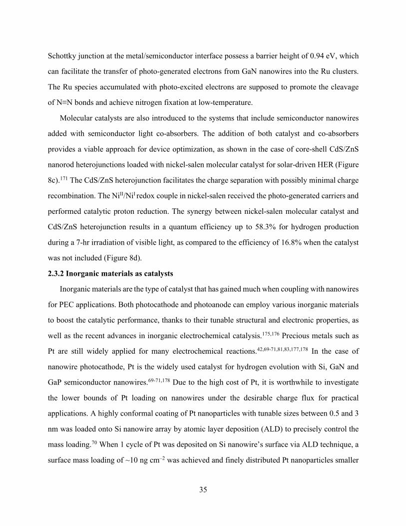
Figure 8. (a) Schematic of the tandem chemical solar cell. Pillars are embedded in a proton conducting membrane. The anode absorbed the blue part of the solar spectrum for oxidizing water into molecular oxygen and protons. The protons migrate through the membrane and are reduced at the cathode side by Mo3S4 clusters adsorbed on the Si pillars, which are excited by the red part of the spectrum. (b) Steady-state current density–voltage (left axis) and calculated IPCE (right axis) for planar and pillared Si with/without Mo3S4 clusters. The almost horizontal dashed lines denote the current measured in darkness. (a-b) Reprinted with permission from ref170. Copyright 2011 Nature Publishing Group. (c) Schematic illustration for the synergystic effect of the CdS/ZnS heterojunction and the water-soluble nickel–salen cocatalyst for enhanced photocatalytic H2 production. (d) The time courses of H2 production (black dot and line) and apparent quantum yield (AQY) (blue bar) over complex 3/CdS/ZnS nanorods photocatalyst. (c-d) Reprinted with permission from ref171. Copyright 2016 John Wiley & Sons, Inc.
In addition to the HER system, molecular/cluster catalysts can be coupled with nanowires for
CO2 reduction. Three kinds of Mn-based carbonyl bipyridyl complexes were tested as molecular
catalysts on Si nanowires.80 Towards the CO2 reduction to CO happened in CH3CN + 5% H2O
(v/v), all nanowire samples loaded with Mn-based complex exhibited higher performance over
their planar counterparts in terms of the fill factor and energy efficiency for the device. Ru clusters
as catalyst was also loaded on the surface of GaN nanowires to assist the reduction of N2 under
light illumination.87 The GaN nanowires exhibited a much higher stability when loaded with ultra-
small Ru sub-nanostructures at high loading density (ca. 1017 m‒2). The authors proposed that the
35
Schottky junction at the metal/semiconductor interface possess a barrier height of 0.94 eV, which
can facilitate the transfer of photo-generated electrons from GaN nanowires into the Ru clusters.
The Ru species accumulated with photo-excited electrons are supposed to promote the cleavage
of N≡N bonds and achieve nitrogen fixation at low-temperature.
Molecular catalysts are also introduced to the systems that include semiconductor nanowires
added with semiconductor light co-absorbers. The addition of both catalyst and co-absorbers
provides a viable approach for device optimization, as shown in the case of core-shell CdS/ZnS
nanorod heterojunctions loaded with nickel-salen molecular catalyst for solar-driven HER (Figure
8c).171 The CdS/ZnS heterojunction facilitates the charge separation with possibly minimal charge
recombination. The NiII/NiI redox couple in nickel-salen received the photo-generated carriers and
performed catalytic proton reduction. The synergy between nickel-salen molecular catalyst and
CdS/ZnS heterojunction results in a quantum efficiency up to 58.3% for hydrogen production
during a 7-hr irradiation of visible light, as compared to the efficiency of 16.8% when the catalyst
was not included (Figure 8d).
2.3.2 Inorganic materials as catalysts
Inorganic materials are the type of catalyst that has gained much when coupling with nanowires
for PEC applications. Both photocathode and photoanode can employ various inorganic materials
to boost the catalytic performance, thanks to their tunable structural and electronic properties, as
well as the recent advances in inorganic electrochemical catalysis.175,176 Precious metals such as
Pt are still widely applied for many electrochemical reactions.42,69-71,81,83,177,178 In the case of
nanowire photocathode, Pt is the widely used catalyst for hydrogen evolution with Si, GaN and
GaP semiconductor nanowires.69-71,178 Due to the high cost of Pt, it is worthwhile to investigate
the lower bounds of Pt loading on nanowires under the desirable charge flux for practical
applications. A highly conformal coating of Pt nanoparticles with tunable sizes between 0.5 and 3
nm was loaded onto Si nanowire array by atomic layer deposition (ALD) to precisely control the
mass loading.70 When 1 cycle of Pt was deposited on Si nanowire’s surface via ALD technique, a
surface mass loading of ~10 ng cm‒2 was achieved and finely distributed Pt nanoparticles smaller
36
than 1 nm were observed on the nanowire’s surface. Despite such small loading amount of Pt, the
deposited nanowire photocathodes still provided the necessary charge flux for solar-to-hydrogen
conversion, therefore quantitatively determines the lower limits of Pt catalysts on high surface area
nanowire photoelectrodes. This work presents a general approach for minimizing the cost of
precious metal catalysts for efficient and affordable solar-to-fuel applications. Precious metals
have also been combined with nanowires for solar-powered reduction of CO2. Guided by the one-
dimensional geometry of Si nanowires, well-dispersed assembly of Au3Cu nanoparticles on their
surfaces was realized.81 The Si nanowires decorated with Au3Cu nanoparticles exhibited high CO2-
to-CO selectivity of about 80% at ‒0.2 V vs reversible hydrogen electrode (RHE), and the
selectivity towards HER has been largely suppressed. Thanks to the optimized spatial arrangement
of Au3Cu nanoparticles on the nanowire arrays, the overpotential for CO2-to-CO conversion has
been reduced by 120 mV as compared to that on planar counterpart. The Pt nanoparticles can also
be utilized somewhat as catalyst to drive the CO2 reduction. By loading Pt nanoparticles onto GaN
nanowire arrays, not only the CO2 reduction rate can be increased, but also the production
selectivity can be switched from CO to CH4. The photoreduction rate of CO2 to CH4 can reach
~14.8 µmol gcat‒1 h‒1 when Pt nanoparticles were on the lateral m-plane surfaces of GaN nanowires,
which is almost an order of magnitude higher than that measured on naked nanowire arrays with
CO as the dominant product.83
In order to deviate from the disadvantages of high cost and low elemental abundance of
precious metals, nanowires have been integrated with a large variety of earth-abundant catalysts,
including transition metals,77,82,137,179 metal oxide,66,180 metal chalcogenides,72,73,181-184 metal
phosphides or phosphates,185-188 metal nitrides,189 metal borides,190 metal hydroxides,164,191 and
metal-free materials.192,193 Among the possible half-reactions that will be of interest to artificial
photosynthesis, the reduction of CO2 and N2 as well as the oxidation of water demand more
assistance with the introduction of catalysts due to their sluggish kinetics.175,176 Moreover,
sometimes two different sorts of inorganic materials, instead of one, were introduced with
nanowires in the hope of obtaining certain synergistic effect among the nanowires and catalysts.
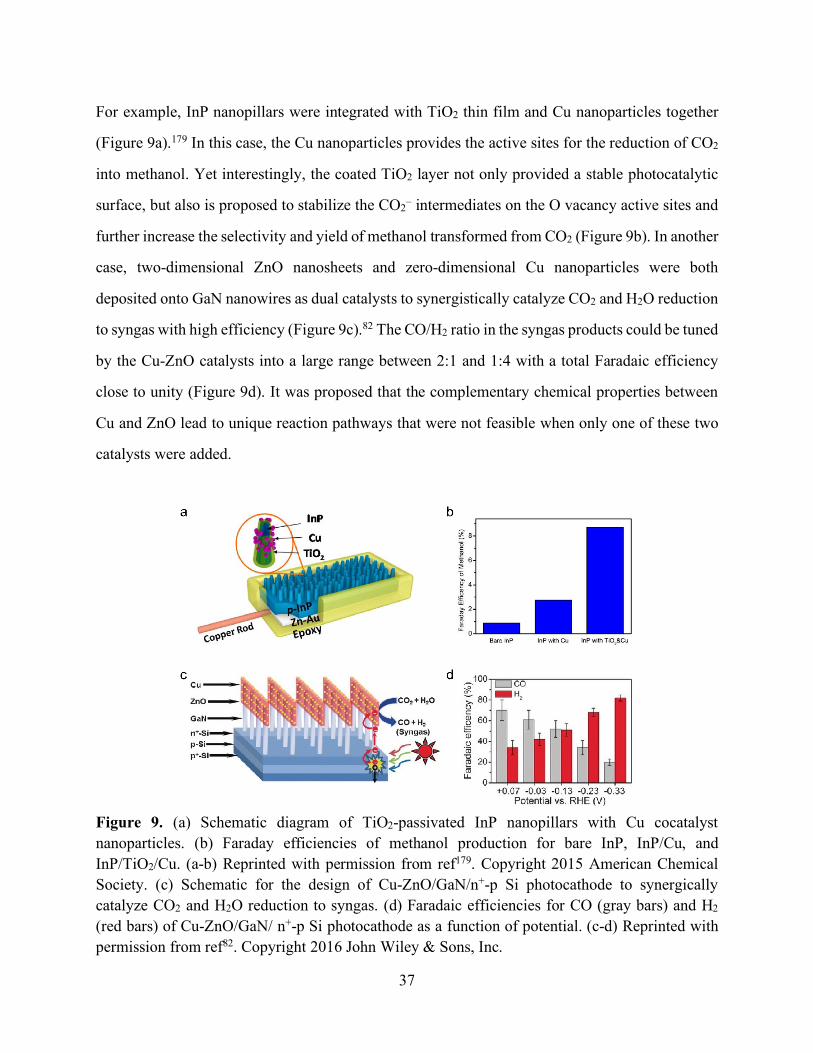
37
For example, InP nanopillars were integrated with TiO2 thin film and Cu nanoparticles together
(Figure 9a).179 In this case, the Cu nanoparticles provides the active sites for the reduction of CO2
into methanol. Yet interestingly, the coated TiO2 layer not only provided a stable photocatalytic
surface, but also is proposed to stabilize the CO2‒ intermediates on the O vacancy active sites and
further increase the selectivity and yield of methanol transformed from CO2 (Figure 9b). In another
case, two-dimensional ZnO nanosheets and zero-dimensional Cu nanoparticles were both
deposited onto GaN nanowires as dual catalysts to synergistically catalyze CO2 and H2O reduction
to syngas with high efficiency (Figure 9c).82 The CO/H2 ratio in the syngas products could be tuned
by the Cu-ZnO catalysts into a large range between 2:1 and 1:4 with a total Faradaic efficiency
close to unity (Figure 9d). It was proposed that the complementary chemical properties between
Cu and ZnO lead to unique reaction pathways that were not feasible when only one of these two
catalysts were added.
Figure 9. (a) Schematic diagram of TiO2-passivated InP nanopillars with Cu cocatalyst nanoparticles. (b) Faraday efficiencies of methanol production for bare InP, InP/Cu, and InP/TiO2/Cu. (a-b) Reprinted with permission from ref179. Copyright 2015 American Chemical Society. (c) Schematic for the design of Cu-ZnO/GaN/n+-p Si photocathode to synergically catalyze CO2 and H2O reduction to syngas. (d) Faradaic efficiencies for CO (gray bars) and H2 (red bars) of Cu-ZnO/GaN/ n+-p Si photocathode as a function of potential. (c-d) Reprinted with permission from ref82. Copyright 2016 John Wiley & Sons, Inc.

38
Inorganic materials have been interfaced with nanowires for solar-powered wastewater
treatment. The degradation of atrazine, a typical herbicide found in both surface and ground waters,
was achieved with Pd4S nanoparticles as the photocatalyst decorated with Bi2S3 nanorods.183
Under visible light irradiation, Pd4S nanoparticles facilitate the charge separation and the delivery
of photo-generated carriers into Bi2S3 nanorods, which serve as active sites with the formation of
hydroxyl radicals for organic decomposition. Pd-decorated Si nanowires was used as photocathode
coupling for light-powered reduction of Cr(VI), a potent toxicant in water. 98.7% Cr(VI) was
efficiently reduced under visible light illumination within 8 h, thanks to the use of Pd nanoparticles
as the catalysts.177
Inorganic materials as catalysts were also frequently coupled with nanowires light-absorbers
in the particulate configuration for photocatalytic reactions.194-198 Pt nanoparticles have been
deposited on CdS nanowires for the application of photocatalytic H2 generation. The yielded
Pt/CdS photocatalysts contained 0.3 wt% of Pt nanoparticle with the size of about 1 to 2 nm, and
displayed promising photocatalytic activity with a 1.49 mmol h‒1 rate of H2 production rate and a
quantum efficiency of 61.7%.194 Two-dimensional MoS2 were incorporated onto TiO2 nanowire
for photocatalytic HER under visible light. With a few layers of MoS2 on porous nanowires of
TiO2, the core-shell hybrid structure was photocatalytically active with a H2-generating rate of
16.7 mmol h‒1 g‒1.195 Last, Zn0.5Cd0.5S nanorods as photocatalyst was decorated with CoP
nanoparticle and exhibited a photocatalytic activity that was not only twenty times higher than that
of pure Zn0.5Cd0.5S sample, but also two times higher than the Zn0.5Cd0.5S sample loaded with
Pt.196 The caveat here is to ensure a suitable loading amount of CoP so that the catalytic proton
reduction was facilitated but the competitive light absorption from CoP was minimized.
2.3.3 Biological moieties as catalysts
Biological entities including enzymatic catalysts or whole cells often exhibit high selectivity
towards a specific reaction process.199 However, they displayed at most moderate solar-to-energy
efficiency at about 0.5% to 2.0%, which is dwarfed by, the values up to 20% that can be achieved

39
by inorganic semiconductors.199 We postulate that a inorganic-biological hybrid that combines
semiconductor light-absorbers with biological catalysts can take the strengths of both and achieve
an efficient and selective process of artificial photosynthesis.33,199,200 The first step towards such
an integration is to investigate the interactions between the inorganic and biological components
at microscopic level. Si nanowire array was applied as real-time imaging platform at the single-
cell level to study the interactions between Si nanowires and Shewanella oneidensis MR-1, a gram-
negative facultative bacterium that was known to facilitate charge transfer with inorganic
materials.201 The presence of nanowire array was recognized by the S. oneidensis MR-1 and
modified the swimming patterns of the microbes as well as the early-stage attachment between the
nanowire and bacteria.201 The physical interaction between bacterial and nanostructures was also
sensitive to the parameters of local environment, including the ionic strength of the electrolyte and
the gas pressure in the headspace. Researchers have studied the interactions between the nanowire
array and the Sporomusa ovata,202 a bioelectrochemically active bacterium that has been reported
to fix CO2 into acetic acid with the supply of electricity from an electrode.203 At high ionic strength
or hydrostatic pressure, S. ovata formed vertically aligned filamentous cells parallel to the
nanowires. Such observation indicate that local environment with the presence of nanowire should
be considered in order to interface nanowires with biocatalysts with good compatibility.
Integrating semiconductor nanowires with S. ovata lead to the a solar-powered device that
reduce CO2 into acetic acid with high selectivity (Figure 10a-b).34 Here the nanowire morphology
provided a large surface area to accommodate S. ovata as the catalyst. Under solar irradiation, the
photo-generated carriers in Si was directly transferred to S. ovata, whose enzymes in the Wood-
Ljungdahl pathway204 take these carriers as reducing equivalents and fix CO2 into acetic acid. This
inorganic-biological hybrid system showed a low overpotential of CO2 fixation (η < 200 mV),
high Faradaic efficiency (up to 90%), and decent long-term stability (up to 200 h). The yielded
acetate, at a titer of about 6 g·L‒1, can be further upgraded by genetically engineered Escherichia
coli for a number of value-added chemicals including n-butanol, polyhydroxybutyrate, and three
different isoprenoid natural products (Figure 10c). In this study, there is one additional benefit for
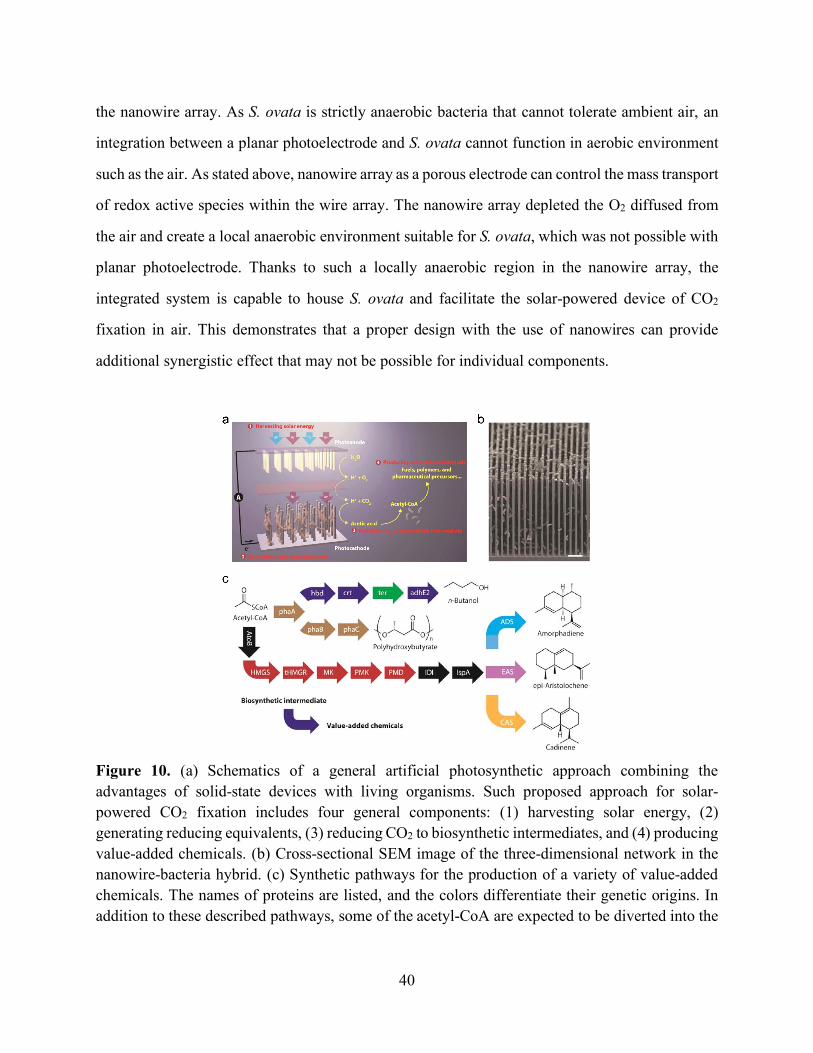
40
the nanowire array. As S. ovata is strictly anaerobic bacteria that cannot tolerate ambient air, an
integration between a planar photoelectrode and S. ovata cannot function in aerobic environment
such as the air. As stated above, nanowire array as a porous electrode can control the mass transport
of redox active species within the wire array. The nanowire array depleted the O2 diffused from
the air and create a local anaerobic environment suitable for S. ovata, which was not possible with
planar photoelectrode. Thanks to such a locally anaerobic region in the nanowire array, the
integrated system is capable to house S. ovata and facilitate the solar-powered device of CO2
fixation in air. This demonstrates that a proper design with the use of nanowires can provide
additional synergistic effect that may not be possible for individual components.
Figure 10. (a) Schematics of a general artificial photosynthetic approach combining the advantages of solid-state devices with living organisms. Such proposed approach for solar-powered CO2 fixation includes four general components: (1) harvesting solar energy, (2) generating reducing equivalents, (3) reducing CO2 to biosynthetic intermediates, and (4) producing value-added chemicals. (b) Cross-sectional SEM image of the three-dimensional network in the nanowire-bacteria hybrid. (c) Synthetic pathways for the production of a variety of value-added chemicals. The names of proteins are listed, and the colors differentiate their genetic origins. In addition to these described pathways, some of the acetyl-CoA are expected to be diverted into the
41
TCA cycle for redox balancing. (a-c) Reprinted with permission from ref34. Copyright 2015 American Chemical Society.
Besides the utilization of biological entities in inorganic-biological hybrid for enhancing the
PEC efficiency of nanowire, the PEC process within nanowire could be used for probing and
modulation of cellular interface and activity.205-207 The potential benefits of nanowire discussed in
section 1.4 could be applicable here. The light-trapping effect and enhanced charge separation
efficacy of nanowire will promote the photoelectrochemical response, and the high surface area
will permit the efficient guest loading and molecule capture.205,206 By growing H9c2 cardiac
myoblasts on nitrogen-doped carbon nanodots (N-Cdots) coupled TiO2 nanowires, a nanomaterial-
cell platform was constructed for photoelectrochemical probing of physiological levels of H2S
messenger generated by living cells.205 The proposed process is the existence of Cu2+ in electrolyte
will quench the charge transfer pathway between N-Cdots and TiO2 nanowires to decrease the
photocurrent to the level of pristine TiO2 nanowire (PEC-off state). Then, the excited H9c2 cardiac
myoblasts can produce H2S to reduce the Cu2+ concentration by forming CuS, which will reinstate
the transfer process of photogenerated charge and thereby increase the photocurrent to the “PEC-
on” stage. The detection sensitivity of H2S in the buffer can reach 10 nM.205 Another study also
adopted TiO2 nanotubes for physiological level probing of H2S.206 The different process is Cd2+
was first adsorbed onto the TiO2 nanotubes, and then the HepG2 cells grown on nanotubes
generated H2S under stimulation to react with Cd2+ into CdS, which will increase the photocurrent
of TiO2 nanotubes by enhancing the light absorption.206
Table 5. Different kinds of catalysts coupled with semiconductor nanowires for various PEC reactions.
Catalyst Nanowire Absorption
wavelength Reaction Electrolyte
J (potential) a / IPCE b
mA cm‒2 / %
FE c
%
EE d
% Ref.
Mo3S4 cluster Si > 620 nm HER 1 M HClO4 9 (URHE = 0) / 93 NA e 10 170 Mn-based
complex Si > 600 nm
CO2
reduction
CH3CN + 5%
v/v H2O NA / NA 0.35 3 80
Pt nanoparticle Si NA HER 0.5 M H2SO4 7 (URHE = 0) / NA NA NA 70
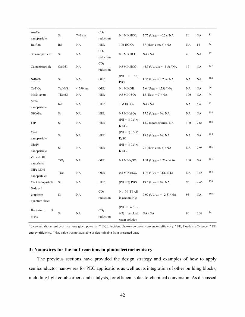
42
Au3Cu
nanoparticle Si 740 nm
CO2
reduction 0.1 M KHCO3 2.75 (URHE = ‒0.2) / NA 80 NA 81
Ru film InP NA HER 1 M HClO4 37 (short circuit) / NA NA 14 42
Sn nanoparticle Si NA CO2
reduction 0.1 M KHCO3 NA / NA 40 NA 77
Cu nanoparticle GaN/Si NA CO2
reduction 0.5 M KHCO3 44.9 (UAg/AgCl = ‒1.5) / NA 19 NA 137
NiRuOx Si NA OER (PH = 7.2)
PBS 1.36 (URHE = 1.23) / NA NA NA 180
CoTiOx Ta3N5/Si < 590 nm OER 0.1 M KOH 2.6 (URHE = 1.23) / NA NA NA 66 MoS2 layers TiO2/Si NA HER 0.5 M H2SO4 15 (URHE = 0) / NA 100 NA 72 MoS3
nanoparticle InP NA HER 1 M HClO4 NA / NA NA 6.4 73
NiCoSex Si NA HER 0.5 M H2SO4 37.5 (URHE = 0) / NA NA NA 184
FeP Si NA HER (PH = 1) 0.5 M
K2SO4 13.9 (short circuit) / NA 100 2.64 188
Co-P
nanoparticle Si NA HER
(PH = 1) 0.5 M
K2SO4 18.2 (URHE = 0) / NA NA NA 185
Ni12P5
nanoparticle Si NA HER
(PH = 1) 0.5 M
K2SO4 21 (short circuit) / NA NA 2.98 186
ZnFe-LDH
nanosheet TiO2 NA OER 0.5 M Na2SO4 1.51 (URHE = 1.23) / 4.86 100 NA 191
NiFe-LDH
nanoplatelet TiO2 NA OER 0.5 M Na2SO4 1.74 (USCE = 0.6) / 5.12 NA 0.58 164
CoB nanoparticle Si NA HER (PH = 7) PBS 19.5 (URHE = 0) / NA 95 2.46 190 N-doped
graphene
quantum sheet
Si NA CO2
reduction
0.1 M TBAH
in acetonitrile 7.07 (UAg/Ag+ = ‒2.5) / NA 95 NA 193
Bacterium S.
ovata Si NA
CO2
reduction
(PH = 6.3 ~
6.7) brackish
water solution
NA / NA 90 0.38 34
a J (potential), current density at one given potential. b IPCE, incident photon-to-current conversion efficiency. c FE, Faradaic efficiency. d EE,
energy efficiency. e NA, value was not available or determinable from presented data.
3: Nanowires for the half reactions in photoelectrochemistry
The previous sections have provided the design strategy and examples of how to apply
semiconductor nanowires for PEC applications as well as its integration of other building blocks,
including light co-absorbers and catalysts, for efficient solar-to-chemical conversion. As discussed
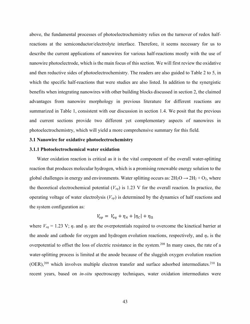
43
above, the fundamental processes of photoelectrochemistry relies on the turnover of redox half-
reactions at the semiconductor/electrolyte interface. Therefore, it seems necessary for us to
describe the current applications of nanowires for various half-reactions mostly with the use of
nanowire photoelectrode, which is the main focus of this section. We will first review the oxidative
and then reductive sides of photoelectrochemistry. The readers are also guided to Table 2 to 5, in
which the specific half-reactions that were studies are also listed. In addition to the synergistic
benefits when integrating nanowires with other building blocks discussed in section 2, the claimed
advantages from nanowire morphology in previous literature for different reactions are
summarized in Table 1, consistent with our discussion in section 1.4. We posit that the previous
and current sections provide two different yet complementary aspects of nanowires in
photoelectrochemistry, which will yield a more comprehensive summary for this field.
3.1 Nanowire for oxidative photoelectrochemistry
3.1.1 Photoelectrochemical water oxidation
Water oxidation reaction is critical as it is the vital component of the overall water-splitting
reaction that produces molecular hydrogen, which is a promising renewable energy solution to the
global challenges in energy and environments. Water splitting occurs as: 2H2O → 2H2 + O2, where
the theoretical electrochemical potential (Veq) is 1.23 V for the overall reaction. In practice, the
operating voltage of water electrolysis (Vop) is determined by the dynamics of half reactions and
the system configuration as:
𝑉R" = 𝑉ST + 𝜂W + |𝜂Y| + 𝜂Z
where Veq = 1.23 V; ηA and ηC are the overpotentials required to overcome the kinetical barrier at
the anode and cathode for oxygen and hydrogen evolution reactions, respectively, and ηΩ is the
overpotential to offset the loss of electric resistance in the system.208 In many cases, the rate of a
water-splitting process is limited at the anode because of the sluggish oxygen evolution reaction
(OER),209 which involves multiple electron transfer and surface adsorbed intermediates.210 In
recent years, based on in-situ spectroscopy techniques, water oxidation intermediates were
44
tentatively probed.211-214 The OER in is generally considered following a four-step single-electron
transfer reaction with three adsorbed intermediates: OH(ad), O(ad), and OOH(ad):
HKO∆^_a OH(4b) + Hc + 𝑒e
OH(4b)∆^fa O(4b) + Hc + 𝑒e
O(4b) + HKO∆^ga OOH(4b) + Hc + 𝑒e
OOH(4b)∆^ha OK + Hc + 𝑒e
The expression of these equations are specific for OER happens under acid condition. The
maximum Gibbs reaction energy of the four primary reactions governs the overpotential of
OER.210 Valdés et al. showed that the OER activity largely depends on the binding strength of
OER intermediates on the catalyst surface.215 In principle, the adsorption energies of reactive
intermediates are controlled by the surface electronic structure of calalyst.208 By adjusting surface
adsorption, it is rational to steer the four primary reactions to optimize the water oxidation
reaction.147,216
Photogenerated holes from semiconductor can be utilized to oxide water to evolve oxygen.
The first demonstration of a photoanode for water oxidation was made by Honda and Fujishima.217
At an external bias of ~0.9 V vs. RHE under UV illumination, 1 mA cm–2 photocurrent density
could be generated on undoped TiO2 photoelectrode. For photoanode made of n-type
semiconductor, water oxidation occurs at the interface between the photoanode and electrolyte.38
When semiconductor photoelectrode is immersed into electrolyte, the Fermi level of
semiconductor will equilibrate with the electrochemical potential of the redox pair, causing band
bending. The built-in interfacial electric field in the space charge region can effectively promote
charge separation for enhanced solar energy conversion efficiency. Photogenerated holes can be
accumulated on the surface of n-type semiconductor under illumination to induce water oxidation
reaction as shown in Figure 11a.38 The potential difference of the anodic photogenerated holes and
cathodic photogenerated electrons should be larger than 1.23 eV for overall water splitting to
overcome the overpotentials in both electrodes.
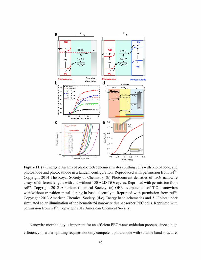
45
Figure 11. (a) Energy diagrams of photoelectrochemical water splitting cells with photoanode, and photoanode and photocathode in a tandem configuration. Reproduced with permission from ref38. Copyright 2014 The Royal Society of Chemistry. (b) Photocurrent densities of TiO2 nanowire arrays of different lengths with and without 150 ALD TiO2 cycles. Reprinted with permission from ref60. Copyright 2012 American Chemical Society. (c) OER overpotential of TiO2 nanowires with/without transition metal doping in basic electrolyte. Reprinted with permission from ref58. Copyright 2013 American Chemical Society. (d-e) Energy band schematics and J−V plots under simulated solar illumination of the hematite/Si nanowire dual-absorber PEC cells. Reprinted with permission from ref63. Copyright 2012 American Chemical Society.
Nanowire morphology is important for an efficient PEC water oxidation process, since a high
efficiency of water-splitting requires not only competent photoanode with suitable band structure,
46
but also eligible surface for adsorption and activation of reaction species. N-type transition metal
oxides and nitrides such as TiO2,60,218 ZnO,61,154 α-Fe2O3,62 WO3,64 Ta3N5,65 and n-type silicon146
nanorod or nanowire arrays and their derivatives have been developed as photoanodes for water
oxidation, which show decent performance in terms of charge transport and carrier collection.
Owing to the one-dimensional morphological feature, nanowire photoanode is able to decouple
the directionality of light absorption and charge transport, as stated in the section 1.4.90,219 The
photo-generated minority carriers in n-type nanowire could transfer to the surface via a short
diffusion pathway along the radial direction to participate in the oxidation reaction with a
significantly enhanced ηseparation, while the morphology of nanowires affords an increased light
absorption.19 Additionally, the nanowire geometry could also provide sufficient sites for catalytic
reactions. Jaramillo et al. demonstrated that the photoelectrochemical water oxidation performance
of core-shell Si-Ta3N5 nanowire photoanode could be greatly improved as compared to the planar
counterpart, owing to the enhanced light absorption and larger electrochemically active surface
area in Si-Ta3N5 nanowires, which are beneficial for water oxidation reaction.66 The integration of
n-type silicon nanowire with Ta3N5 could shift the photocurrent onset to more negative potentials
owing to an “improved” band alignment.66 In another example, Ta3N5 nanowire photoanode
displayed an enhanced OER photocurrent up to 3.2 fold at 1.23 V vs. RHE compared with its thin-
film counterparts, thanks to its large surface active area, the short diffusion length of photoexcited
holes, and the enhanced light absorption with suppressed reflection as discussed in section 1.4.65
Moreover, WO3/W:BiVO4 nanowire photoanode achieved a OER photocurrent density of 3.1 mA
cm–2 and an 60% IPCE at 300–450 nm, both at 1.23 V vs. RHE.64 Such a decent
photoelectrochemical performance is attributed to the higher value of charge separation efficiency
(ηseparation) and the efficient charge transfer at surface in WO3/W:BiVO4 nanowire photoanode.64
Besides the advantages brought by morphological features, surface properties of nanowires are
also important in PEC cells as they directly influence charge recombination and chemical reaction
kinetics. Hwang et al. reported that both the length and surface properties of TiO2 nanowires had
strong impacts on their PEC performances of water oxidation (Figure 11b).60 Since here nanowire
47
photoanode acted as both the light absorbers and catalytic sites, it is important to find a balance
between light harvesting and catalytic reaction to optimize the photoanode’s performance.
Additionally, the addition of catalyst should be considered when the kinetic of water oxidation
could be the bottleneck. For example, hematite nanowires have advantages of visible light
absorption, large abundance and low cost, but with high overpotential for water oxidation.
Consequently, it is necessary to apply catalyst to improve kinetics of oxygen evolution on
hematite.147 As such, surface and interface engineering are indispensable as discussed in Section
2, in which catalysts play a crucial role at lowering the reaction barrier and improving charge
separation efficiency. Moreover, the doping of hetero-atoms and the establishment of
heterojunction in nanowire photoanode are commonly used to optimize surface properties, which
can promote charge kinetics and facilitate surface reaction. Under visible light illumination (400–
475 nm), an apparent quantum efficiency of the incident photons (ηPEC) of 12.3% was achieved for
overall wireless water-splitting in neutral aqueous medium, with the use of core/shell Rh/Cr2O3
decorated double-band p-GaN/p-In0.2Ga0.8N nanowire heterojunction photoelectrode.153 Under
concentrated sunlight, the establishment of GaN/InGaN heterojunction and the introduction of
Rh/Cr2O3 catalysts led to a production rate of H2 and O2 as high as 3.46 mol h–1 g–1 and 1.69 mol
h–1 g–1, respectively.153 For TiO2 nanowire array photoanode, the coating of CdS later lead to
distinctive shift of the photocurrent onset potential, from –0.297 V to –0.403 V vs. Ag/AgCl.
Additional coating of cobalt phosphate OER catalyst could further shift the onset potential to –
0.469 V vs. Ag/AgCl.59 Here, it was proposed by the authors that the introduction of CdS layer
leads to a negative shift of Fermi level, while the addition of cobalt phosphate catalysts suppressed
charge recombination around the flat-band potential and subsequently improved the kinetics for
OER.59 Transition-metal dopants were demonstrated to be helpful in lowering overpotential of
OER in rutile TiO2 nanowires resulting from enhanced adsorption of OER intermediates (Figure
11c).58 Wang et al. established a Z-scheme Si@α-Fe2O3 dual-absorber system, which could absorb
photons in a wide spectrum and promote charge separation through band engineering (Figure 11d-
e).63 In this system, different doping levels of silicon nanowires at 1014, 1016, and 1018 cm–3 could
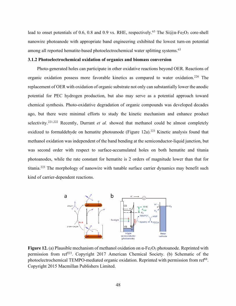
48
lead to onset potentials of 0.6, 0.8 and 0.9 vs. RHE, respectively.63 The Si@α-Fe2O3 core-shell
nanowire photoanode with appropriate band engineering exhibited the lowest turn-on potential
among all reported hematite-based photoelectrochemical water splitting systems.63
3.1.2 Photoelectrochemical oxidation of organics and biomass conversion
Photo-generated holes can participate in other oxidative reactions beyond OER. Reactions of
organic oxidation possess more favorable kinetics as compared to water oxidation.220 The
replacement of OER with oxidation of organic substrate not only can substantially lower the anodic
potential for PEC hydrogen production, but also may serve as a potential approach toward
chemical synthesis. Photo-oxidative degradation of organic compounds was developed decades
ago, but there were minimal efforts to study the kinetic mechanism and enhance product
selectivity.221,222 Recently, Durrant et al. showed that methanol could be almost completely
oxidized to formaldehyde on hematite photoanode (Figure 12a).223 Kinetic analysis found that
methanol oxidation was independent of the band bending at the semiconductor-liquid junction, but
was second order with respect to surface-accumulated holes on both hematite and titania
photoanodes, while the rate constant for hematite is 2 orders of magnitude lower than that for
titania.223 The morphology of nanowire with tunable surface carrier dynamics may benefit such
kind of carrier-dependent reactions.
Figure 12. (a) Plausible mechanism of methanol oxidation on α-Fe2O3 photoanode. Reprinted with permission from ref223. Copyright 2017 American Chemical Society. (b) Schematic of the photoelectrochemical TEMPO-mediated organic oxidation. Reprinted with permission from ref68. Copyright 2015 Macmillan Publishers Limited.
49
Additionally, the efficient oxidation conversion of renewable biomass to valuable chemicals
has attracted considerable attention in fundamental studies and for practical applications. Assisted
by BiVO4 photoanode, a 2,2,6,6-tetramethylpiperidine 1-oxyl (TEMPO)-mediated 5-
hydroxymethylfurfural (HMF) oxidation into 2,5-furandicarboxylic acid (FDCA) was
demonstrated by Choi et al. (Figure 12b).68 The Faradaic efficiency of the TEMPO-mediated
biomass conversion process can reach as high as 93%, suggesting that TEMPO oxidation is
kinetically faster than water oxidation on BiVO4. Without TEMPO medium, the HMF oxidation
into FDCA was also completed by Sun et al. using Ni based electrocatalysts, and near-unity
Faradaic efficiencies were achieved for the generation of hydrogen and FDCA.224,225 Liu et al.
developed a PEC system on porous BiVO4 nanoarray photoanode for the selective oxidation of
glycerol to value-added 1,3-dihydroxyacetone (DHA) without catalysts and redox mediator.67 A
photocurrent density of 3.7 mA cm–2 and an apparent quantum efficiency of the incident photons
(ηPEC) of 25% for 400-nm photon at 1.2 V vs. RHE were achieved in acidic electrolyte. Meanwhile,
this photoanode could produce 56 mmol gcatalyst–1 h–1 of DHA with a DHA selectivity of 64 %.
Faster reaction kinetics of PEC glycerol oxidation than water oxidation was demonstrated in this
work. This nanoarray photoanode could produce DHA with higher rate and selectivity than thin-
film photoanode. The authors attributed these features to the electrode’s large surface area,
abundant active sites, and probably the adequate mass transport (section 1.4).67 By combining
photovoltaics and catalytic reactions, they also established a biomass photo-reforming cell that is
able to simultaneously produce hydrogen and chemical.226 Nanowire photoanodes that have
distinct advantages at charge kinetics and light absorption may be particularly useful for
photoelectrochemical organic oxidation and biomass conversion.
3.2 Nanowire for reductive photoelectrochemistry
As the other half of the overall Z-scheme solar-to-fuel process, PEC cathodic reactions are
equally important.227-229 In a photocathodic process, the photo-generated electrons transport to the
catalytic sites for chemical reactions at the interface between photocathode and electrolyte. A
reasonably good photocathode should provide relatively large photovoltage given it band-gap, a
50
decent and stable photocurrent, and last but not least, high reaction selectivity of the desirable
products under an acceptable overpotential.230 Due to the unique structural, physical and chemical
properties, photocathodes composed of semiconductor nanowires have demonstrated several
advantages over planar ones, which have been summarized in previous section.12 In the following
section, we will review the recent research efforts in developing semiconductor nanowire
photocathodes for PEC hydrogen evolution, CO2 reduction and N2 reduction, respectively.
3.2.1 Photoelectrochemical hydrogen evolution
PEC hydrogen production has attracted a lot of research interests since Fujishima and Honda
demonstrated the first solar water splitting process with TiO2 photoelectrode in 1972.217 With the
introduction of the Z-scheme dual-light-absorber design, relatively small-band-gap semiconductor
materials such as Si and III-V group materials have been intensively investigated for
photoelectrochemical hydrogen evolution.230
Si is widely considered a promising photocathode material for solar H2 evolution, because it is
earth-abundant, relatively stable, has suitable band gap for light absorption and conduction band
edge for HER reaction.231 However, as an indirect bandgap material, planar Si electrode typically
suffers high reflection loss and requires a ~200 µm thickness to absorb the longer-wavelength light.
On the other hand, Si wires decouple the light absorption and the charge carrier collection,232 and
at the same time bring the light trapping effect within the array, which significantly reduce the
light reflection loss.219 In addition, taking advantage of their large surface area, Si nanowire array
photocathode allows the use of earth-abundant HER electrocatalyst instead of the precious noble
metal electrocatalyst.4 Oh et al. reported that p-type Si nanowires photocathode prepared via
electroless etching yielded a photovoltage as high as 420 mV, and significantly outperformed the
planar counterpart due to the reduced overpotential and light trapping effect.69 P. Yang’s group
and D. Wang’s group both reported that Pt can be deposited onto Si nanowire photocathode via
the ALD method.70,71 Precisely controlling the amount of Pt loading as low as ~10 ng cm–2 (Figure
13a), such approach represents a general method to minimize the cost of noble metal HER catalyst
for efficient photoelectrochemical H2 production (Figure 13b). Zhang et al. showed the integration

51
of earth-abundant MoS2 HER electrocatalysts onto the high-surface area Si nanowire array
photocathode.72 A decent onset potential of ~0.3 V vs. RHE was obtained, owing to the reduced
surface flux of electrons that can be handled by MoS2 electrocatalysts.
Figure 13. (a) Scanning transmission electron microscopy (STEM) image of Pt nanoparticles deposited on a Si nanowire by ALD. (b) HER performance of Si nanowire array photocathode with different ALD Pt loadings. (a-b) Reprinted with permission from ref70. Copyright 2013 American Chemical Society. (c) Schematics of synthesis and purification of colloidal GaP nanowires. Reprinted with permission from ref178. Copyright 2011 American Chemical Society.
The benefits obtained from Si nanowire are also applicable to photocathodes composed of III-
V nanowires. Lee et al. reported that p-type InP nanopillars can dramatically increase the solar-to-
hydrogen efficiency to 14%, compared with 9% of the planar counterpart.42 Such enhancement
results from the low reflection loss and efficient charge separation originated from the nanopilliar
structure. It was also found that the InP nanopillars facilitate the desorption of H2 bubbles, which
in turn promote the H2 evolution by reducing the reverse effect of local H2 molecules. In addition,
E. Bakkers’s group used vapor-liquid-solid (VLS) method to grow vertically aligned p-type InP
and GaP nanowire arrays with a small surface parking fraction.73,74 Loaded with noble-metal-free
52
MoSx HER electrocatalysts, these nanowire photocathodes can achieve higher energy conversion
efficiency than planar analogues. Such high performance is attributed to the efficient charge
separation in the high-quality III-V nanowires and the fast electron transfer at the nanowire/MoSx
interface. In addition to the benefits mentioned above, III-V nanowires also feature low-cost
synthesis, compared to the expensive fabrication of planar III-V wafer. Sun et al. discovered that
colloidal GaP nanowires can be synthesized via a low-cost solution-liquid-solid (SLS) method
(Figure 13c).178 These GaP nanowires can be conveniently drop-cast on a conductive substrate and
carry out solar H2 production for at least 12 hours. Furthermore, these GaP nanowires can be
controllably doped by introducing Zn dopants during the SLS synthesis.91 By optimizing the
nanowire diameter and the Zn doping concentration, the doped GaP nanowires exhibit better
absorbed photon-to-current efficiency (APCE) than planar GaP, with only 1/3000 of the amount
of material used in the planar cathode. In addition, the nanowire geometry allows for the flexible
multijunction design of III-V photocathode, which synergistically combines the advantages of III-
V materials with different compositions. Fan et al. reported a monolithically integrated
photocathode that is composed of p-InGaN/tunnel junction/n-GaN nanowire arrays on a planar
n+p Si substrate.233 Such nanowire-based lateral multijunction circumvents the current
mismatching issue typically present in conventional buried multijunction photocathode, and thus
allows the photo-generated electrons at different segments to drive HER reaction at the same time.
As a result, this system yielded an impressive 40 mA cm–2 photocurrent density, with a near-unity
faraday efficiency of H2.
In addition to Si and III-V materials, metal oxides, in particular Cu2O and CuO, are also
considered as promising photocathode for solar H2 production, owing to their relatively small
bandgap, suitable conduction band edge, earth abundance and simple synthesis procedure.
However, because of the severe mismatch between the minority carrier diffusion length (20-200
nm) and the absorption depth (~2 µm), the planar copper oxide photocathode typically suffers low
values of IPCE, especially at longer radiation wavelength. To solve such problem, Huang et al.
prepared highly aligned Cu2O nanowire arrays, and found that the photocurrent of Cu2O nanowires
53
doubled that of the planar electrode, largely due to the efficient collection of photogenerated
electrons along the nanowire’s radial direction.76 After protected by a CuO/TiO2 shell, the resulting
Cu2O/CuO/TiO2 core-shell nanowire structure gained 74% more photocurrent and 4.5 times higher
stability. Moreover, Luo et al. developed a phase-controlled synthesis method to grow high-quality
Cu2O nanowire arrays with superior optoelectronic properties.75 Such Cu2O nanowire
photocathode can achieve photocurrent as high as 10 mA cm–2, and a better IPCE than planar
counterpart for wavelength ranging from 350 nm to 650 nm.
3.2.2 Photoelectrochemical reduction of carbon dioxide
With the rise of CO2 concentration in the atmosphere and the resulting climate issue, research
in the field of catalytic CO2 conversion has grown rapidly in the past decades.234
Photoelectrochemical CO2 reduction, where the dissolved CO2 molecules are reduced at the
photocathode/electrolyte interface, is considered a promising approach to realizing efficient CO2
conversion.235 However, photoelectrochemical CO2 reduction on a planar photoelectrode typically
suffers low energy-conversion efficiency, because the sluggish kinetics of CO2 activation and
conversion determines that typically a large overpotential is needed to drive the reaction.236 In
addition, the overall reaction process involves multiple proton coupled electron transfer steps,
leading to a low selectivity of the desirable carbon products.237 Photocathodes made of
semiconductor nanowires provide opportunities to mitigate these challenges. In addition to the
benefits regarding efficient charge transport and enhanced light absorption that observed in solar
H2 production process, the large surface area of the nanowire geometry in principle can gain more
benefits in terms of the reduced overpotential for CO2 reduction. Furthermore, the multifaceted
nature of semiconductor nanowires and the unique mass transport of redox species within the
nanowire arrays can also have an impact on the multi-step CO2 reduction and thus bring further
benefits to the CO2 conversion efficiency. In this section, we will review the recent progress on
photoelectrochemical CO2 reduction using semiconductor nanowires as the light absorber. Based
on the nature of the catalytic reaction, both homogeneous and heterogeneous process will be briefly
discussed.
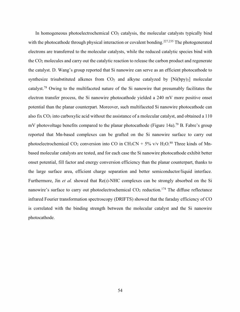
54
In homogeneous photoelectrochemical CO2 catalysis, the molecular catalysts typically bind
with the photocathode through physical interaction or covalent bonding.227,235 The photogenerated
electrons are transferred to the molecular catalysts, while the reduced catalytic species bind with
the CO2 molecules and carry out the catalytic reaction to release the carbon product and regenerate
the catalyst. D. Wang’s group reported that Si nanowire can serve as an efficient photocathode to
synthesize trisubstituted alkenes from CO2 and alkyne catalyzed by [Ni(bpy)2] molecular
catalyst.78 Owing to the multifaceted nature of the Si nanowire that presumably facilitates the
electron transfer process, the Si nanowire photocathode yielded a 240 mV more positive onset
potential than the planar counterpart. Moreover, such multifaceted Si nanowire photocathode can
also fix CO2 into carboxylic acid without the assistance of a molecular catalyst, and obtained a 110
mV photovoltage benefits compared to the planar photocathode (Figure 14a).79 B. Fabre’s group
reported that Mn-based complexes can be grafted on the Si nanowire surface to carry out
photoelectrochemical CO2 conversion into CO in CH3CN + 5% v/v H2O.80 Three kinds of Mn-
based molecular catalysts are tested, and for each case the Si nanowire photocathode exhibit better
onset potential, fill factor and energy conversion efficiency than the planar counterpart, thanks to
the large surface area, efficient charge separation and better semiconductor/liquid interface.
Furthermore, Jin et al. showed that Re(ɪ)-NHC complexes can be strongly absorbed on the Si
nanowire’s surface to carry out photoelectrochemical CO2 reduction.174 The diffuse reflectance
infrared Fourier transformation spectroscopy (DRIFTS) showed that the faraday efficiency of CO
is correlated with the binding strength between the molecular catalyst and the Si nanowire
photocathode.
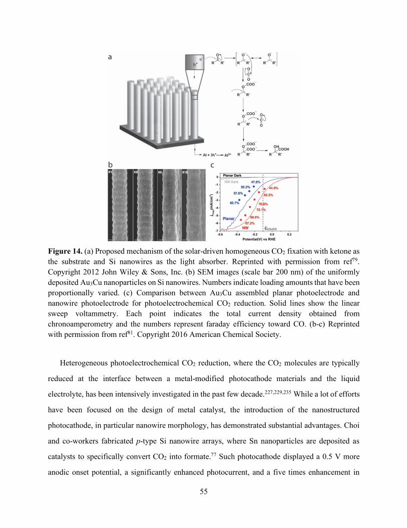
55
Figure 14. (a) Proposed mechanism of the solar-driven homogeneous CO2 fixation with ketone as the substrate and Si nanowires as the light absorber. Reprinted with permission from ref79. Copyright 2012 John Wiley & Sons, Inc. (b) SEM images (scale bar 200 nm) of the uniformly deposited Au3Cu nanoparticles on Si nanowires. Numbers indicate loading amounts that have been proportionally varied. (c) Comparison between Au3Cu assembled planar photoelectrode and nanowire photoelectrode for photoelectrochemical CO2 reduction. Solid lines show the linear sweep voltammetry. Each point indicates the total current density obtained from chronoamperometry and the numbers represent faraday efficiency toward CO. (b-c) Reprinted with permission from ref81. Copyright 2016 American Chemical Society.
Heterogeneous photoelectrochemical CO2 reduction, where the CO2 molecules are typically
reduced at the interface between a metal-modified photocathode materials and the liquid
electrolyte, has been intensively investigated in the past few decade.227,229,235 While a lot of efforts
have been focused on the design of metal catalyst, the introduction of the nanostructured
photocathode, in particular nanowire morphology, has demonstrated substantial advantages. Choi
and co-workers fabricated p-type Si nanowire arrays, where Sn nanoparticles are deposited as
catalysts to specifically convert CO2 into formate.77 Such photocathode displayed a 0.5 V more
anodic onset potential, a significantly enhanced photocurrent, and a five times enhancement in
56
formate production in comparison with the planar counterpart, thanks to the reduced reflectance
and efficient electron transfer along the radial direction of the Si nanowire. Kong et al. reported
that the Si nanowire arrays can guide the uniform spatial arrangement of Au3Cu nanoparticles on
the nanowire’s surface (Figure 14b), while the nanoparticles tend to form isolated islands on a
planar Si electrode.81 A reduced overpotential of 120 mV compared to the planar counterpart was
observed originated from the well-dispersed assembly of nanoparticles on the nanowire’s surface
(Figure 14c). Such well-defined semiconductor-catalyst interface enables efficient
photoelectrochemical CO2 reduction to CO, with the faraday efficiency close to 80% at –0.2 V vs.
RHE. Efforts have also been put to investigate photoelectrochemical CO2 reduction on III-V
nanowire materials. Qiu et al. claimed that TiO2-passivated InP nanopillars can reduce CO2 into
methanol with a faraday efficiency of 4.79%.179 It was suggested that the O vacancies at the TiO2
surface can facilitate the formation of CO2– intermediate and thus serve as catalytically active sites
in the CO2 reduction process. Deposition of Cu nanoparticle catalysts on the InP nanopillar’s
surface can further enhance the methanol faraday efficiency up to 8.7%. Mi’s group has actively
studied photoelectrochemical CO2 reduction on GaN nanowires that modified by different metal
nanoparticles. Taking advantage of the low defect density and high surface area of the GaN
nanowires, it was shown that the as-grown nanowires can photocatalytically reduce CO2 into CO,
while the introduction of the Pt catalyst significantly enhances the CH4 production by nearly one
order of magnitude.83 Such enhancement is attributed to the effective separation of the hot carriers
and the reduction of CO2 activation barrier by Pt nanoparticles. Furthermore, it was shown that
deposition of metal catalyst on the oxide-passivated GaN nanowires can photoelectrochemically
produce syngas with tunable ratio between CO and H2. Specifically, Chu et al. fabricated a
Cu/ZnO/GaN nanowire structure and obtained syngas products with CO/H2 ratio ranging from 2:1
to 1:4.82 Impressively, a high faraday efficiency of 70% for CO was observed at overpotential as
low as 180 mV. It was suggested that such efficient syngas production is attributed to the
synergistic co-catalytic effect between ZnO and Cu. Chu et al. further improved the
photoelectrochemical syngas production by sequential deposition of Pt nanoparticles and ultrathin
57
TiO2 on the GaN nanowires.84 As the Pt/TiO2 interface provides multifunctional sites for CO2
activation and conversion, the resulting structure yielded a solar-to-syngas efficiency of 0.87%, a
high turnover number of 24800 and a wide-range CO/H2 ratio between 4:1 and 1:6. In order to
circumvent the use of noble-metal catalyst, Rajeshwar and co-workers developed a two-step
approach to synthesize the CuO/Cu2O core-shell nanorod array photocathode.85 An impressive
faraday efficiency of 95% toward methanol can be realized at an underpotential greater than 150
mV. Such efficient CO2 conversion is attributed to double electron transfer pathway from both the
CuO core and the Cu2O shell to the CO2 molecules in the electrolyte. Taking advantage of the
superior activity and product selectivity, biological catalysts recently have been integrated with
semiconductor materials for solar-driven CO2 conversion. Liu et al. reported that Si nanowires can
serve as a bio-compatible photocathode to interface with Sporomusa Ovata to specifically convert
CO2 into acetic acid.34 Compare to the planar counterpart, the unique nanowire geometry prevents
the diffusion of the O2 molecules, and thus provide an O2-free local environment for the anaerobic
bacteria to live and function.
3.2.3 Photoelectrochemical and photocatalytic reduction of dinitrogen
Ammonia (NH3) is essential in agriculture and many industry processes. The invention of
Haber-Bosch process to synthesize NH3 from N2 and H2 has greatly changed the way that the food
is produced, and contributed ~50% of the N atoms in humans today.176 However, as high
temperature (~700 K) and high pressure (~100 atm) are both required in the Haber-Bosch process,
it is very energy-intensive and consumes nearly 2% of the annual energy output in the world. As
a result, great efforts have been made to search for alternative approaches to synthesizing NH3 at
mild conditions. Photoelectrochemical/photocatalytic N2 reduction, where N2 molecules are
reduced at the semiconductor/liquid electrolyte interface with solar energy as the reaction driving
force, represents a sustainable strategy for NH3 synthesis.228 However, the inertness of N≡N triple-
bond, the sluggish reaction kinetics and the lack of efficient catalyst lead to major challenges for
this reaction, especially the high overpotential and the poor selectivity of NH3 over H2.238,239
Nanostructuring the semiconductor light absorber, particularly into a 1D nanowire/nanorod
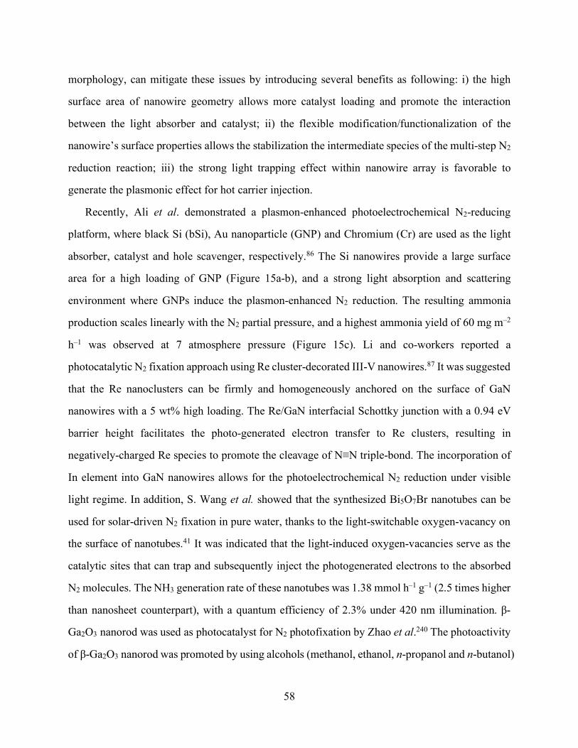
58
morphology, can mitigate these issues by introducing several benefits as following: i) the high
surface area of nanowire geometry allows more catalyst loading and promote the interaction
between the light absorber and catalyst; ii) the flexible modification/functionalization of the
nanowire’s surface properties allows the stabilization the intermediate species of the multi-step N2
reduction reaction; iii) the strong light trapping effect within nanowire array is favorable to
generate the plasmonic effect for hot carrier injection.
Recently, Ali et al. demonstrated a plasmon-enhanced photoelectrochemical N2-reducing
platform, where black Si (bSi), Au nanoparticle (GNP) and Chromium (Cr) are used as the light
absorber, catalyst and hole scavenger, respectively.86 The Si nanowires provide a large surface
area for a high loading of GNP (Figure 15a-b), and a strong light absorption and scattering
environment where GNPs induce the plasmon-enhanced N2 reduction. The resulting ammonia
production scales linearly with the N2 partial pressure, and a highest ammonia yield of 60 mg m–2
h–1 was observed at 7 atmosphere pressure (Figure 15c). Li and co-workers reported a
photocatalytic N2 fixation approach using Re cluster-decorated III-V nanowires.87 It was suggested
that the Re nanoclusters can be firmly and homogeneously anchored on the surface of GaN
nanowires with a 5 wt% high loading. The Re/GaN interfacial Schottky junction with a 0.94 eV
barrier height facilitates the photo-generated electron transfer to Re clusters, resulting in
negatively-charged Re species to promote the cleavage of N≡N triple-bond. The incorporation of
In element into GaN nanowires allows for the photoelectrochemical N2 reduction under visible
light regime. In addition, S. Wang et al. showed that the synthesized Bi5O7Br nanotubes can be
used for solar-driven N2 fixation in pure water, thanks to the light-switchable oxygen-vacancy on
the surface of nanotubes.41 It was indicated that the light-induced oxygen-vacancies serve as the
catalytic sites that can trap and subsequently inject the photogenerated electrons to the absorbed
N2 molecules. The NH3 generation rate of these nanotubes was 1.38 mmol h–1 g–1 (2.5 times higher
than nanosheet counterpart), with a quantum efficiency of 2.3% under 420 nm illumination. β-
Ga2O3 nanorod was used as photocatalyst for N2 photofixation by Zhao et al.240 The photoactivity
of β-Ga2O3 nanorod was promoted by using alcohols (methanol, ethanol, n-propanol and n-butanol)
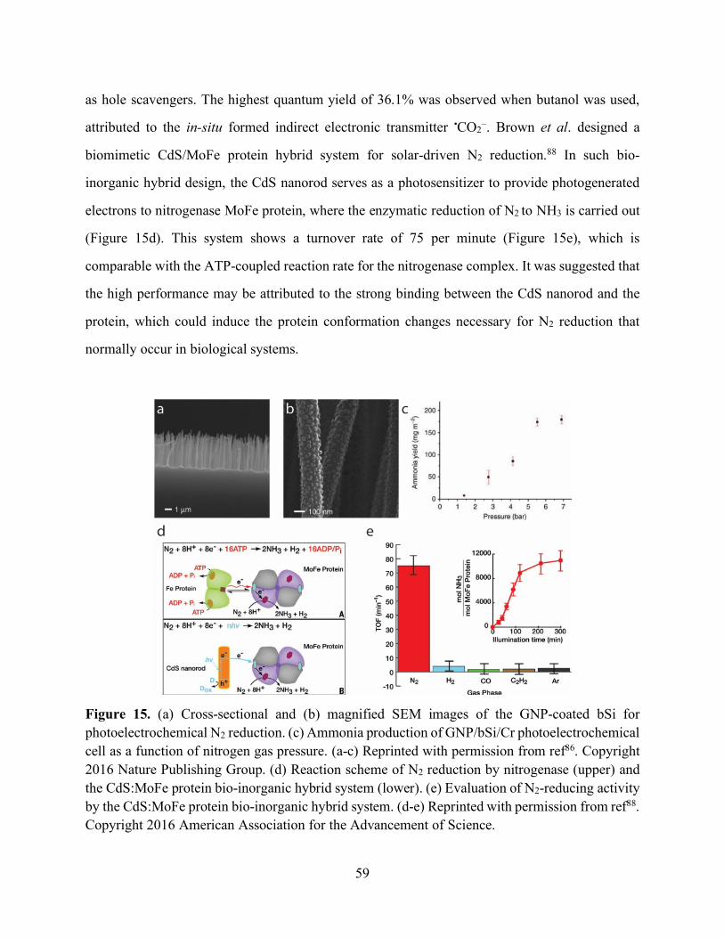
59
as hole scavengers. The highest quantum yield of 36.1% was observed when butanol was used,
attributed to the in-situ formed indirect electronic transmitter •CO2–. Brown et al. designed a
biomimetic CdS/MoFe protein hybrid system for solar-driven N2 reduction.88 In such bio-
inorganic hybrid design, the CdS nanorod serves as a photosensitizer to provide photogenerated
electrons to nitrogenase MoFe protein, where the enzymatic reduction of N2 to NH3 is carried out
(Figure 15d). This system shows a turnover rate of 75 per minute (Figure 15e), which is
comparable with the ATP-coupled reaction rate for the nitrogenase complex. It was suggested that
the high performance may be attributed to the strong binding between the CdS nanorod and the
protein, which could induce the protein conformation changes necessary for N2 reduction that
normally occur in biological systems.
Figure 15. (a) Cross-sectional and (b) magnified SEM images of the GNP-coated bSi for photoelectrochemical N2 reduction. (c) Ammonia production of GNP/bSi/Cr photoelectrochemical cell as a function of nitrogen gas pressure. (a-c) Reprinted with permission from ref86. Copyright 2016 Nature Publishing Group. (d) Reaction scheme of N2 reduction by nitrogenase (upper) and the CdS:MoFe protein bio-inorganic hybrid system (lower). (e) Evaluation of N2-reducing activity by the CdS:MoFe protein bio-inorganic hybrid system. (d-e) Reprinted with permission from ref88. Copyright 2016 American Association for the Advancement of Science.
60
4. Fundamentals of photoelectrochemistry at single-nanowire level
Although considerable research efforts have been focused on studying nanowire array
photoelectrode, the heterogeneity in geometry, doping, defects density and catalyst loading
typically present in such arrays can obscure the link between these properties and the
photoelectrochemical performance of the nanowires, and correlating performance with the specific
properties of individual nanowires is difficult because of the ensemble averaging.241,242 In addition,
the physical and chemical interactions between individual nanowires within the arrays, such as the
light scattering and the diffusion of redox species, can significantly convolute our understanding
on the nanowire’s native properties and the fundamental reaction mechanisms.243
By overcoming the inhomogeneity found in arrays of nanowires, a single semiconductor
nanowire device can provide a more precise link between the nanowire’s properties and its
photoelectrochemical/photocatalytic performance. By comparing the performance of individual
nanowires with that of the ensemble arrays, we can in turn understand the impact of the
inhomogeneity on the ensemble systems. In addition, controlling a single nanowire’s properties,
such as its geometry relative to the characteristic length scales of many fundamental processes that
occur on the nano- and microscale, enables systematic investigations to determine the intrinsic
limits of performance and optimal design of nanowire photoelectrodes. Moreover, a single-
nanowire device can be flexibly coupled with other advanced characterization techniques, such as
single-molecule fluorescence spectroscopy,244,245 to understand the electron transport process and
uncover the reaction mechanisms at the semiconductor/electrolyte interface. In this section, we
will first discuss the state-of-art single-nanowire devices for photoelectrochemical
characterizations beyond the ensemble averaging. In addition, we will also review the progress of
single-molecule, single-particle fluorescence spectroscopy that can be used to uncover the reaction
mechanisms during the photo(electro)catalytic process.
4.1 Single-nanowire photoelectrochemistry
A device composed of a single nanowire, a well-defined platform suitable for studying basic
physical and chemical processes at the nanoscopic level, has been applied in electronics,35 bio-
61
probing,246 photovoltaics,247,248 thermoelectrics249 and electrochemistry.250 Single-nanowire
photoelectrochemistry is particularly challenging, because it requires the sophisticated
manipulation of the device structure in order to avoid the interaction between individual nanowires
and the contribution from the substrate. Recently, the Yang’s group reported a unique single-
nanowire photoelectrode platform (Figure 16a), which can reliably probe the photoelectrochemical
behavior of individual nanowires.251 Via the VLS approach, the single Si nanowires are vertically
grown on electrically isolated Si electrodes, enabling the characterization of each nanowire
individually (Figure 16b). The J-V characteristics yielded decent photoelectrochemical behavior
with picoampere photocurrent sensitivity and tunable photovoltage output for devices with
different doping profiles. In contrast to the inhomogeneity present in nanowire arrays, the well-
defined geometry of a single nanowire in this study allows for the quantification of the
photogenerated electron flux over the nanowire’s surface, and provides quantitative information
on the reduced overpotential owing to the nanowire’s large surface area (Figure 16d). In addition,
the authors observed that the photovoltage of the nanowire array devices is comparable with the
lowest photovoltage of single nanowires (Figure 16c), indicating that the performance of ensemble
array photoelectrode is largely affected by the worst performing individual nanowires within the
array. This observation highlights the importance of controlling the homogeneity of the
nanomaterials’ quality, in order to produce efficient nanowire-based solar-to-fuel devices.
Recently, Zhang et al. also reported single-nanowire photoelectrode device that is fabricated
horizontally on the substrate.92 By systematically tuning the diameter of the individual nanowires
from 200 nm to 2000 nm, it was suggested that the diameter of 1415 nm yielded the highest solar
energy conversion efficiency. The wavelength-dependent IPCE measurements suggested that the
efficiency of single-nanowire photoelectrodes is determined by the diameter-dependent light
absorption. Moreover, the photoelectrochemical behavior of individual nanowires can also be used
to modulate the cellular activity. The Tian’s group recently reported that the photocathodic effect
generated by coaxial single nanowires can be harnessed to elicit action potentials in neuronal
cells.207 Taking advantage of patch-clamp setup, the photocurrent of free-standing individual
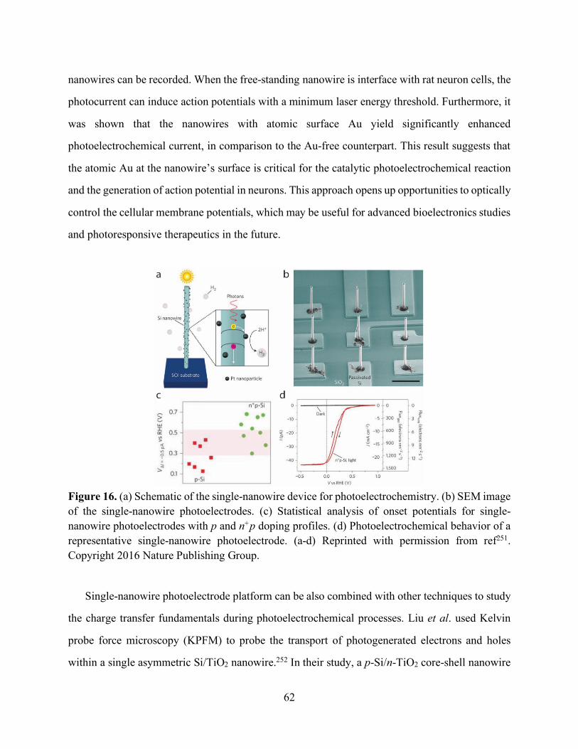
62
nanowires can be recorded. When the free-standing nanowire is interface with rat neuron cells, the
photocurrent can induce action potentials with a minimum laser energy threshold. Furthermore, it
was shown that the nanowires with atomic surface Au yield significantly enhanced
photoelectrochemical current, in comparison to the Au-free counterpart. This result suggests that
the atomic Au at the nanowire’s surface is critical for the catalytic photoelectrochemical reaction
and the generation of action potential in neurons. This approach opens up opportunities to optically
control the cellular membrane potentials, which may be useful for advanced bioelectronics studies
and photoresponsive therapeutics in the future.
Figure 16. (a) Schematic of the single-nanowire device for photoelectrochemistry. (b) SEM image of the single-nanowire photoelectrodes. (c) Statistical analysis of onset potentials for single-nanowire photoelectrodes with p and n+p doping profiles. (d) Photoelectrochemical behavior of a representative single-nanowire photoelectrode. (a-d) Reprinted with permission from ref251. Copyright 2016 Nature Publishing Group.
Single-nanowire photoelectrode platform can be also combined with other techniques to study
the charge transfer fundamentals during photoelectrochemical processes. Liu et al. used Kelvin
probe force microscopy (KPFM) to probe the transport of photogenerated electrons and holes
within a single asymmetric Si/TiO2 nanowire.252 In their study, a p-Si/n-TiO2 core-shell nanowire
63
is designed to explore the feasibility for direct solar water splitting, where the n-type TiO2 and p-
Si are proposed to behave as photoanode and photocathode, respective. Under illumination, KPFM
observed higher surface potential on the n-TiO2 shell, relative to the potential of the p-Si nanowire.
This result suggests that the photogenerated holes and electrons tend to accumulate at n-TiO2 and
p-Si, respectively, with the recombination of majority carrier at the Si/TiO2 interface. The efficient
charge separation and transport indicate that the p-Si/n-TiO2 core-shell nanowire is a promising
building block for unassisted tandem solar water splitting. Spectroscopic techniques have also been
employed to quantitatively investigate the photoinduced charge separation within a single-
nanowire photo(electro)catalyst. In 2009, the Majima’s group studied the behavior of
photogenerated charge carriers in individual TiO2 nanowires using photoluminescence (PL)
spectroscopy.253 The time trajectory of the PL intensity showed numerous burst-like features,
which is believed to originate from the radiative recombination of electrons and holes at the color
centers, such as the oxygen vacancies in TiO2 nanowires. The quenching of the burst-like PL
phenomenon with increased O2 concentration suggests that the free electrons are quenched by the
absorbed O2 molecules following a Langmuir-Hinshelwood model. The potential-dependent PL
spectra further revealed that the trapping sites are involved in the potential-induced PL process,
and the energy level of the trapped electrons is considered to be –0.1 V to –0.3V vs. SHE. Moreover,
the detection of the remote PL indicates long-distance transport of charge carriers, which can be
explained by a trapping-detrapping model.
In addition to the representative techniques mentioned above, other characterization
approaches including scanning electrochemical microscopy,254 scanning photocurrent
microscopy255 and ultrafast transient absorption spectroscopy256 have been widely applied to study
the photoelectrochemical behavior on planar and nanowire array photoelectrodes. The integration
between the state-of-art single-nanowire photo(electro)catalyst with these advanced
characterization techniques may open up new opportunities to obtain further deep insights into the
photoelectrochemical process.
4.2 Single-molecule, single-particle fluorescence spectroscopy
64
Although the single-nanowire photoelectrode platform is capable of obtaining nanoscopic
insights that beyond the ensemble averaging, it can’t provide comprehensive information
regarding the photo(electro)catalytic reaction mechanisms. In addition, the heterogeneous
distribution of defect and active sites within a single nanowire can blur our understanding on the
defect/active site-dependent electron transfer process.257 On the other hand, single molecule
fluorescence spectroscopy is a powerful tool to image the fundamental
photoelectrochemical/photochemical process with down to nanometer spatial resolution.244,245 As
a result, the combination of single-molecule fluorescence imaging with single-nanowire
photoelectrode platform represents an intriguing approach to study the charge carrier activities of
the photo(electro)catalysts with the highest possible sensitivity and spatial resolution. Here, we
will give a brief review on the recent progress of single-molecule, single-particle fluorescence
spectroscopy, with the focus on the one-dimensional TiO2 photo(electro)catalysts.
In 2009, the Majima’s group first reported the single-molecule imaging of photocatalytic
reactions on a one-dimensional TiO2 nanotube photocatalyst (Figure 17a).258 A specific
fluorescence probe, aminophenyl fluorescein (APF), was used to detect the hydroxyl radicals (•OH)
generated during the photocatalytic process. When DMSO is added as a •OH quencher, the
fluorescence intensity is completely suppressed (Figure 17b). Distinguishable fluorescence time
trajectories were observed for fluorescein products present in macropores and mesopores,
indicating the positive correlation between the product diffusion rate and the pore size. In addition,
the spatial-resolved fluorescence intensity on a single TiO2 nanotube suggests a heterogeneous
distribution of the active sites, which may be attributed to the intrinsic distribution of surface
defects such as oxygen vacancies during the sample preparation. Single-molecule fluorescence
imaging has widely been used to study the photocatalytic reaction mechanisms, particularly on
individual TiO2 nanorod photo(electro)catalyst. In 2012, Xu et al. found that the trapped holes and
electrons on individual TiO2 nanorod can both serve as active sites to produce the fluorescent
molecules, while the trapped holes show relatively higher activity.259 Specifically, the
photogenerated electrons and hole can react with absorbed O2 and H2O molecules to yield O2–• and
65
OH• radicals, respectively, which can both react with non-fluorescent amplex red to form the
fluorescent product resorufin. By quenching one kind radical while keeping the other active, the
activity of each radical can be separately identified. The fluorescence trajectory, coupled with the
Langmuir-Hinshelwood model, quantitatively revealed that the absorption coefficient and net
reactivity for reactions with OH• as the oxidant have higher values than those with O2–• as the
oxidant. These results can be explained by the positively-charged microenvironment around the
trapped holes, which significantly enhance the absorption of the negatively-charged substrate
molecules. In 2016, the Chen’s group designed a single-TiO2-nanorod photoanode platform, where
the photoelectrooxidation mechanisms can be identified with single-molecule fluorescence.260 By
quantitatively characterizing the substrate oxidation rate as a function of the applied potential and
light intensity, it was found that the oxidation rate scales with (I0)1/2 and (E)1/4. Such correlation is
consistent with the Gärtner model, and suggests that the organic substrate was oxidized indirectly
via OH• radicals instead of directly by photogenerated holes. Furthermore, Sambur et al. reported
that the single-molecule fluorescence imaging can provide guidance for rational engineering the
catalysts on the surface of the TiO2 photoanode.261 Taking advantage of the super-resolution
imaging, the authors statistically analyzed the surface reaction rates along individual TiO2 nanorod
under different applied potentials (Figure 17c). By detecting the number of local fluorescence
products in a certain period, it was found that the sites with high hole-induced reaction rates at
more positive potentials also show high electron-induced reaction rates at more negative potentials.
This result suggests that the photogenerated holes and electrons tend to reach the same sites on the
TiO2 nanorod surface, and thus the most active sites for water oxidation may also promote the
electron-hole recombination. Furthermore, in order to quantify the benefits of the catalysts, oxygen
evolution catalyst (OEC) was photoelectrochemically deposited onto either high- or low-activity
sites that have been identified. By characterizing the onset potential and absorbed-photon-to-
current efficiency (ƞ) before and after the OEC deposition on a specific site, it was suggested that
the locations with lowest initial activities achieve the most photocurrent enhancement or most
reduced onset potentials from the OEC deposition. And the enhancement in photocurrent is not
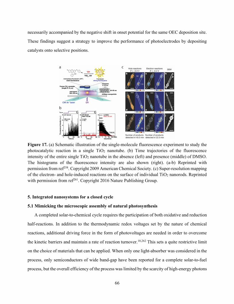
66
necessarily accompanied by the negative shift in onset potential for the same OEC deposition site.
These findings suggest a strategy to improve the performance of photoelectrodes by depositing
catalysts onto selective positions.
Figure 17. (a) Schematic illustration of the single-molecule fluorescence experiment to study the photocatalytic reaction in a single TiO2 nanotube. (b) Time trajectories of the fluorescence intensity of the entire single TiO2 nanotube in the absence (left) and presence (middle) of DMSO. The histograms of the fluorescence intensity are also shown (right). (a-b) Reprinted with permission from ref258. Copyright 2009 American Chemical Society. (c) Super-resolution mapping of the electron- and hole-induced reactions on the surface of individual TiO2 nanorods. Reprinted with permission from ref261. Copyright 2016 Nature Publishing Group.
5. Integrated nanosystems for a closed cycle
5.1 Mimicking the microscopic assembly of natural photosynthesis
A completed solar-to-chemical cycle requires the participation of both oxidative and reduction
half-reactions. In addition to the thermodynamic redox voltages set by the nature of chemical
reactions, additional driving force in the form of photovoltages are needed in order to overcome
the kinetic barriers and maintain a rate of reaction turnover.10,262 This sets a quite restrictive limit
on the choice of materials that can be applied. When only one light-absorber was considered in the
process, only semiconductors of wide band-gap have been reported for a complete solar-to-fuel
process, but the overall efficiency of the process was limited by the scarcity of high-energy photons
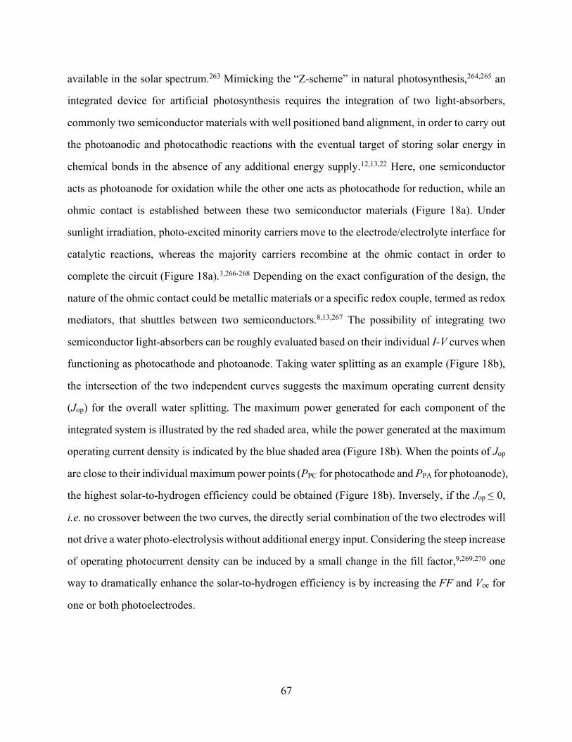
67
available in the solar spectrum.263 Mimicking the “Z-scheme” in natural photosynthesis,264,265 an
integrated device for artificial photosynthesis requires the integration of two light-absorbers,
commonly two semiconductor materials with well positioned band alignment, in order to carry out
the photoanodic and photocathodic reactions with the eventual target of storing solar energy in
chemical bonds in the absence of any additional energy supply.12,13,22 Here, one semiconductor
acts as photoanode for oxidation while the other one acts as photocathode for reduction, while an
ohmic contact is established between these two semiconductor materials (Figure 18a). Under
sunlight irradiation, photo-excited minority carriers move to the electrode/electrolyte interface for
catalytic reactions, whereas the majority carriers recombine at the ohmic contact in order to
complete the circuit (Figure 18a).3,266-268 Depending on the exact configuration of the design, the
nature of the ohmic contact could be metallic materials or a specific redox couple, termed as redox
mediators, that shuttles between two semiconductors.8,13,267 The possibility of integrating two
semiconductor light-absorbers can be roughly evaluated based on their individual I-V curves when
functioning as photocathode and photoanode. Taking water splitting as an example (Figure 18b),
the intersection of the two independent curves suggests the maximum operating current density
(Jop) for the overall water splitting. The maximum power generated for each component of the
integrated system is illustrated by the red shaded area, while the power generated at the maximum
operating current density is indicated by the blue shaded area (Figure 18b). When the points of Jop
are close to their individual maximum power points (PPC for photocathode and PPA for photoanode),
the highest solar-to-hydrogen efficiency could be obtained (Figure 18b). Inversely, if the Jop ≤ 0,
i.e. no crossover between the two curves, the directly serial combination of the two electrodes will
not drive a water photo-electrolysis without additional energy input. Considering the steep increase
of operating photocurrent density can be induced by a small change in the fill factor,9,269,270 one
way to dramatically enhance the solar-to-hydrogen efficiency is by increasing the FF and Voc for
one or both photoelectrodes.
68
Figure 18. (a) Illustration of the “Z-scheme” by using two kinds of semiconductors with different band gaps. The photogenerated minority carriers move to the surface to drive a reduction (left) or oxidation (right) reaction, while the majority carriers recombine at the interface that linking the two semiconductors. (b) Compositive current-potential curves for both photocathode and photoanode with water splitting as an example. Thermodynamic potentials for H+/H2 and O2/H2O are presented as the dashed lines. Jop stands for the maximum operating current density, PPC and PPA stand for the individual maximum power points of photocathode and photoanode, respectively. Red shaded areas highlight the maximum power generated for each component of the integrated system, while blue shaded area highlights the power generated at the maximum operating current density.
The first report that mimics the “Z-scheme” concept for artificial photosynthesis is proposed
by Art Nozik in the 1970s.271 The central concept is to construct a photochemical diode by coupled
two small bandgap materials as photocathode and photoanode, mimicking photosystems I and II
in natural photosynthesis, for unassisted solar water splitting. The increased photocurrent as
compared to the case of a single semicondutor,21,47 promises spontaneous solar water splitting with
high energy efficiencies. Such a design has inspired researchers in the passing decades and here
we would like to provide some updates about the cases that nanowire photoelectrochemistry was
applied.
5.2 Integrated artificial photosynthesis and its design principle
In the integrated “Z-scheme”, charge carriers travel through both semiconductors in a tandem
fashion. Therefore at working conditions the photocurrent flux from the photoanode and
photocathode is the same. This indicates that an optimized device of high energy efficiency should
have suitable band gaps and band alignments for both materials. Theoretical calculations have
predicted that a pair of photoelectrodes with band gaps of approximately 1.1 and 1.7 eV should be
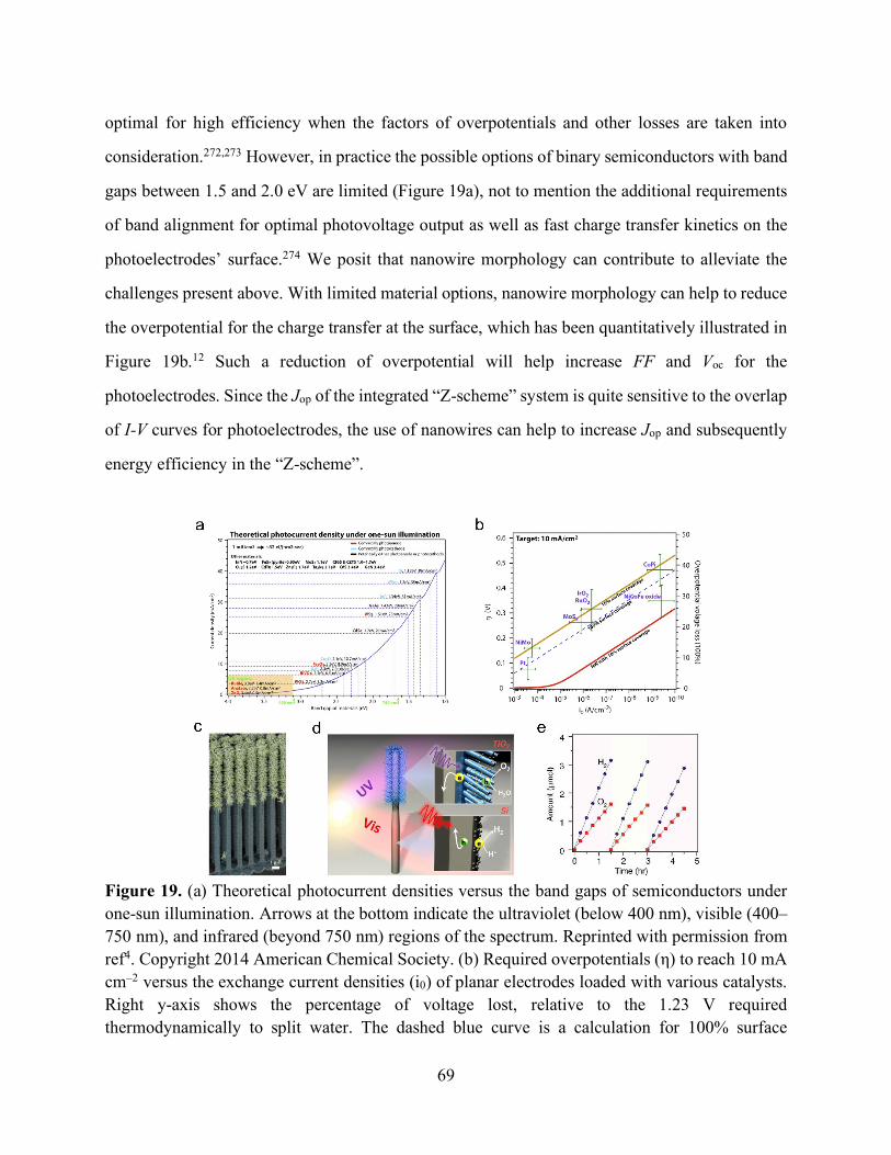
69
optimal for high efficiency when the factors of overpotentials and other losses are taken into
consideration.272,273 However, in practice the possible options of binary semiconductors with band
gaps between 1.5 and 2.0 eV are limited (Figure 19a), not to mention the additional requirements
of band alignment for optimal photovoltage output as well as fast charge transfer kinetics on the
photoelectrodes’ surface.274 We posit that nanowire morphology can contribute to alleviate the
challenges present above. With limited material options, nanowire morphology can help to reduce
the overpotential for the charge transfer at the surface, which has been quantitatively illustrated in
Figure 19b.12 Such a reduction of overpotential will help increase FF and Voc for the
photoelectrodes. Since the Jop of the integrated “Z-scheme” system is quite sensitive to the overlap
of I-V curves for photoelectrodes, the use of nanowires can help to increase Jop and subsequently
energy efficiency in the “Z-scheme”.
Figure 19. (a) Theoretical photocurrent densities versus the band gaps of semiconductors under one-sun illumination. Arrows at the bottom indicate the ultraviolet (below 400 nm), visible (400–750 nm), and infrared (beyond 750 nm) regions of the spectrum. Reprinted with permission from ref4. Copyright 2014 American Chemical Society. (b) Required overpotentials (η) to reach 10 mA cm‒2 versus the exchange current densities (i0) of planar electrodes loaded with various catalysts. Right y-axis shows the percentage of voltage lost, relative to the 1.23 V required thermodynamically to split water. The dashed blue curve is a calculation for 100% surface
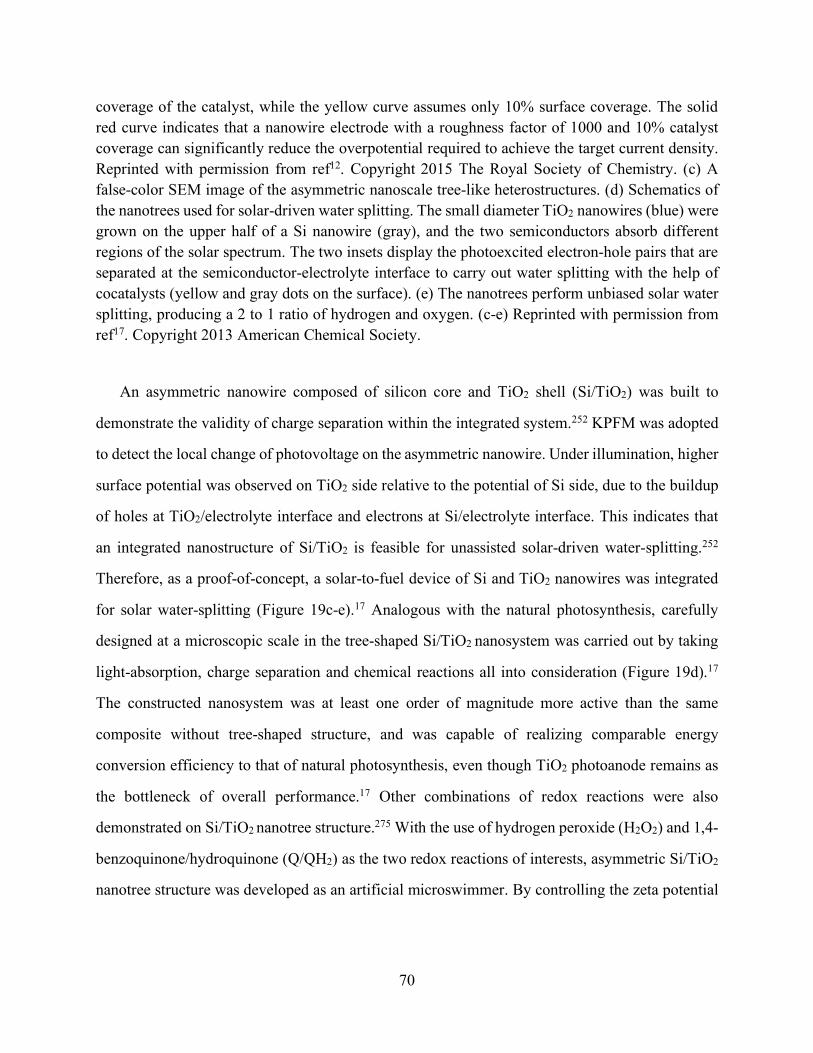
70
coverage of the catalyst, while the yellow curve assumes only 10% surface coverage. The solid red curve indicates that a nanowire electrode with a roughness factor of 1000 and 10% catalyst coverage can significantly reduce the overpotential required to achieve the target current density. Reprinted with permission from ref12. Copyright 2015 The Royal Society of Chemistry. (c) A false-color SEM image of the asymmetric nanoscale tree-like heterostructures. (d) Schematics of the nanotrees used for solar-driven water splitting. The small diameter TiO2 nanowires (blue) were grown on the upper half of a Si nanowire (gray), and the two semiconductors absorb different regions of the solar spectrum. The two insets display the photoexcited electron-hole pairs that are separated at the semiconductor-electrolyte interface to carry out water splitting with the help of cocatalysts (yellow and gray dots on the surface). (e) The nanotrees perform unbiased solar water splitting, producing a 2 to 1 ratio of hydrogen and oxygen. (c-e) Reprinted with permission from ref17. Copyright 2013 American Chemical Society.
An asymmetric nanowire composed of silicon core and TiO2 shell (Si/TiO2) was built to
demonstrate the validity of charge separation within the integrated system.252 KPFM was adopted
to detect the local change of photovoltage on the asymmetric nanowire. Under illumination, higher
surface potential was observed on TiO2 side relative to the potential of Si side, due to the buildup
of holes at TiO2/electrolyte interface and electrons at Si/electrolyte interface. This indicates that
an integrated nanostructure of Si/TiO2 is feasible for unassisted solar-driven water-splitting.252
Therefore, as a proof-of-concept, a solar-to-fuel device of Si and TiO2 nanowires was integrated
for solar water-splitting (Figure 19c-e).17 Analogous with the natural photosynthesis, carefully
designed at a microscopic scale in the tree-shaped Si/TiO2 nanosystem was carried out by taking
light-absorption, charge separation and chemical reactions all into consideration (Figure 19d).17
The constructed nanosystem was at least one order of magnitude more active than the same
composite without tree-shaped structure, and was capable of realizing comparable energy
conversion efficiency to that of natural photosynthesis, even though TiO2 photoanode remains as
the bottleneck of overall performance.17 Other combinations of redox reactions were also
demonstrated on Si/TiO2 nanotree structure.275 With the use of hydrogen peroxide (H2O2) and 1,4-
benzoquinone/hydroquinone (Q/QH2) as the two redox reactions of interests, asymmetric Si/TiO2
nanotree structure was developed as an artificial microswimmer. By controlling the zeta potential
71
of nanotree through chemical modification, the microswimmers with positive or negative
phototaxis can be both successfully programmed.275,276
Materials combination other than Si and TiO2 has been reported for unassisted solar water-
splitting. Indium phosphide (InP) has been considered as a promising alternative to Si because of
its relatively narrow bandgap (1.35-1.42 eV),42,73 while bismuth vanadate (BiVO4) shows
advantages as photoanode materials with a relatively small band-gap.17 InP nanowires have been
integrated with nanoporous BiVO4 for an overall reaction of water splitting at neutral pH.277 The
system generated 0.82 ± 0.04 mA per two electrodes with an area of 1 cm2 each, corresponding to
a solar-to-fuel efficiency of 0.5% for water splitting.277
A concept of bilayer nanowire fabrics was purposed in order to construct a low-cost and
flexible PEC integrated system with facile production separation (Figure 20a).21,47 In this design,
the photoanode and photocathode, both made of nanowire meshes with high surface area, are
physically connected for an ohmic contact. A proton transport medium will be placed between
these two electrodes, and matching of current density is demanded to efficiently utilize the solar
spectrum. A bilayer Ru/Rh-SrTiO3 and BiVO4 nanowire mesh film for unassisted solar overall
water splitting was constructed as a proof of concept (Figure 20b-c). By employing such a bilayer
nanowire mesh, it is possible to achieve simultaneous production and separation of H2 an O2 at the
Ru/Rh-SrTiO3 side and BiVO4 side, respectively.48 The Ru/Rh-SrTiO3-BiVO4 interface and the
balance in light absorption by each nanowire mesh are both important for the H2/O2 evolution.48
Additional effort such as the use of other semiconductor materials or the addition of conductive
additives including graphene sheets and metallic carbon nanotubes, will potentially increase the
overall reactivity of the integrated nanowire systems.48
72
Figure 20. (a) Schematic illustration (left) and a zoomed-in view (right) of a bilayer nanowire fabric-based composite membrane for direct solar water-splitting. The top layer is a high-surface-area nanowire mesh decorated with oxidation catalysts. This part serves as a photoanode responsible for water oxidation; the bottom layer is a high-surface-area nanowire mesh decorated with reduction catalysts. This is the photocathode responsible for water reduction. Reprinted with permission from ref47. Copyright 2012 Nature Publishing Group. (b) Cross-sectional SEM image of bilayer Rh-SrTiO3 and BiVO4 nanowire mesh interface with illustration of the overall water splitting process. (c) Overall water splitting into hydrogen (■) and oxygen (●) using bilayer Ru/Rh-SrTiO3 and BiVO4 nanowire mesh film. (b-c) Reprinted with permission from ref48. Copyright 2014 American Chemical Society.
6. Conclusion and outlooks
The above discussions provide a summary of nanowire photoelectrochemistry. We examined
the potential benefits of nanowires in photoelectrochemistry, different strategies that have been
adopted when interfacing nanowires with other building blocks in artificial photosynthesis, and
the current development of utilizing nanowires for a solar-powered chemical transformation. Since
the inception of applying nanowires for photoelectrochemistry in 2002,18 significant advances
have taken place both at fundamental level and for practical applications. With so many excellent
works that have been done, the question that we are now facing is: what’s the next? In this section,
we will not rephrase the benefits and achievements that have been discovered. Instead we strive to
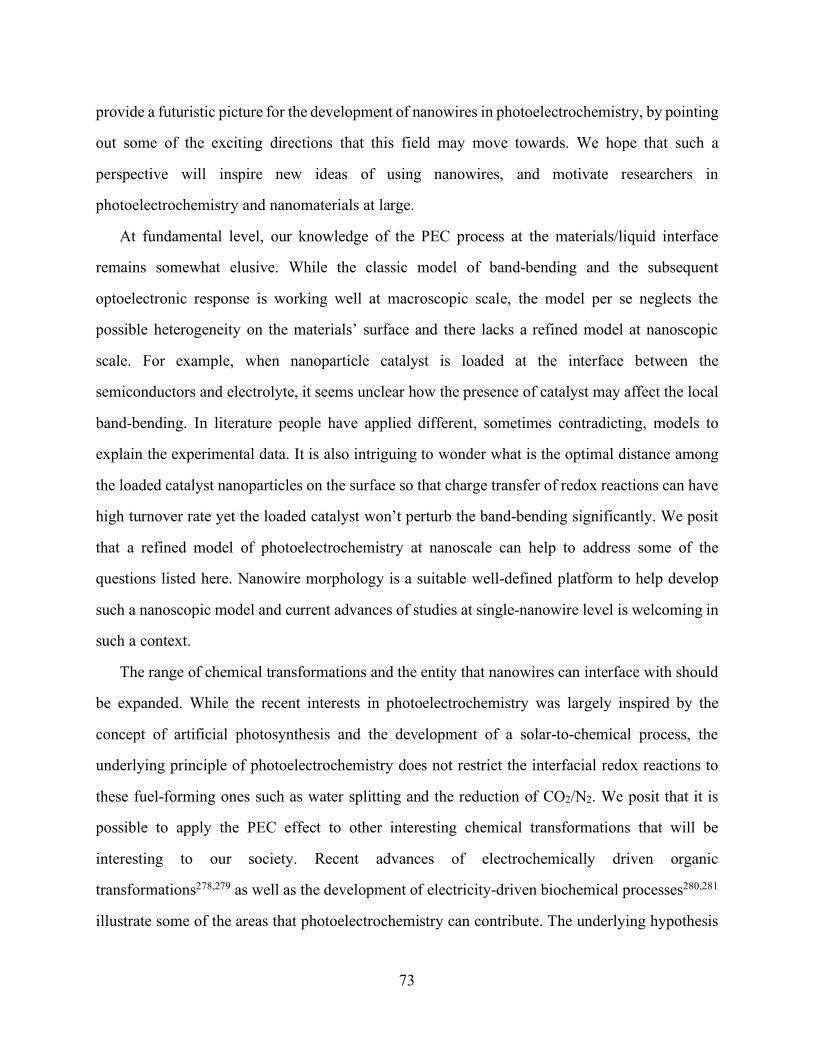
73
provide a futuristic picture for the development of nanowires in photoelectrochemistry, by pointing
out some of the exciting directions that this field may move towards. We hope that such a
perspective will inspire new ideas of using nanowires, and motivate researchers in
photoelectrochemistry and nanomaterials at large.
At fundamental level, our knowledge of the PEC process at the materials/liquid interface
remains somewhat elusive. While the classic model of band-bending and the subsequent
optoelectronic response is working well at macroscopic scale, the model per se neglects the
possible heterogeneity on the materials’ surface and there lacks a refined model at nanoscopic
scale. For example, when nanoparticle catalyst is loaded at the interface between the
semiconductors and electrolyte, it seems unclear how the presence of catalyst may affect the local
band-bending. In literature people have applied different, sometimes contradicting, models to
explain the experimental data. It is also intriguing to wonder what is the optimal distance among
the loaded catalyst nanoparticles on the surface so that charge transfer of redox reactions can have
high turnover rate yet the loaded catalyst won’t perturb the band-bending significantly. We posit
that a refined model of photoelectrochemistry at nanoscale can help to address some of the
questions listed here. Nanowire morphology is a suitable well-defined platform to help develop
such a nanoscopic model and current advances of studies at single-nanowire level is welcoming in
such a context.
The range of chemical transformations and the entity that nanowires can interface with should
be expanded. While the recent interests in photoelectrochemistry was largely inspired by the
concept of artificial photosynthesis and the development of a solar-to-chemical process, the
underlying principle of photoelectrochemistry does not restrict the interfacial redox reactions to
these fuel-forming ones such as water splitting and the reduction of CO2/N2. We posit that it is
possible to apply the PEC effect to other interesting chemical transformations that will be
interesting to our society. Recent advances of electrochemically driven organic
transformations278,279 as well as the development of electricity-driven biochemical processes280,281
illustrate some of the areas that photoelectrochemistry can contribute. The underlying hypothesis
74
is that unique chemical reactivities can arise from the band-bending and charge transfer processes
in photoelectrochemistry, which is not available in other possible alternatives. Nanowire should
gain a prominent role in the development of these PEC systems, as the large surface area of
nanowires can magnify these proposed unique reactivities. In order to facilitate these proposed
chemical transformations, a broader range of building blocks should be interfaced on the nanowire
with a higher level of control at various length scales. While current research has demonstrated the
interaction between nanowires with catalytic molecules, inorganic nanomaterials, and biocatalysts,
there remains much room of advancement to fine-tune the interfacial interaction between them.
Last, sophisticated engineering and fabrication should continuously be devoted for a functional
device. The natural photosynthetic system not only has the “Z-scheme” design that captures
sunlight and yield energy-rich chemicals, but also contains the membrane that spatially separate
the oxidation and reduction products. While a similar design has been envisioned for a while,2,3
there haven’t been a nanowire-based system that fully mimic both the solar chemistry and
membrane-based separation of chemical products. The integration of nanowire building for a
closed cycle in artificial photosynthesis has achieved much advance, yet additional efforts should
be direct for a functional device. More broadly speaking, such an engineering effort at a system
level47 should not be limited only to the application of artificial photosynthesis, as any practical
applications rely on the detailed design and system optimization.
Overall, even though here we present a “review” on the topic of nanowires in
photoelectrochemistry, this article should not be a mere summary but a cornerstone for the
scientific discoveries and breakthroughs in the future. The unique properties of nanowire
photoelectrochemistry remain to be further explored. As Richard Feynman said, “there is plenty
of room at the bottom”, we posit that there is plenty of room for nanowire photoelectrochemistry
so that this can be one of the tools that our society will wield against the challenges in energy,
environment, and sustainability.

75
Author information
Corresponding authors
Emails: [email protected] (P. Y.); [email protected] (B. L.); [email protected] (C.
L.)
ORCID
Jiao Deng: 0000-0003-1008-6795
Yude Su: 0000-0002-3553-9458
Dong Liu: 0000-0002-3588-8762
Peidong Yang: 0000-0003-4799-1684
Bin Liu: 0000-0002-4685-2052
Chong Liu: 0000-0001-5546-3852
Present address
§ (Y. S.) Department of Chemistry, University of California, Santa Barbara
Notes
The authors declare no competing financial interests.
76
Biographies
Dr. Jiao Deng received his B. S. in Chemistry from Sichuan University, China in 2010. Under the
supervision of Prof. Xinhe Bao and Prof. Dehui Deng, he obtained his Ph. D. degree in Physical
chemistry in 2015 at Dalian Institute of Chemical Physics, Chinese Academy of Sciences. His PhD
thesis focused on two-dimensional materials for renewable catalysis. After a short tenure as an
iChEM postdoctoral fellow at Xiamen University, Dr. Deng joined at 2017 as a postdoctoral fellow
in Prof. Chong Liu’s lab at the University of California, Los Angeles. His current research focuses
on the electrocatalytic activation and conversion of small molecules.
Dr. Yude Su earned his bachelor’s degree in Chemistry from University of Science and
Technology of China in 2012. He joined Professor Peidong Yang’s group and received his Ph.D.
degree from the Department of Chemistry at U.C. Berkeley in 2017. He is currently a postdoctoral
scholar working with Professor Guillermo Bazan in Center for Polymer and Organic Solids at U.C.
Santa Barbara. His research interests include development of novel inorganic-biological hybrid
systems for energy-conversion and energy-storage applications.
Dr. Dong Liu received his B.S. in chemistry (Special Class for the Gifted Young) in 2012, and
Ph.D. in inorganic chemistry (Hefei National Laboratory for Physical Sciences at the Microscale)
in 2017 from the University of Science and Technology of China. He is currently a research fellow
in Prof. Bin Liu’s research group at Nanyang Technological University. His research interests
focus on developing solar-driven catalysis for valuable fuels and chemicals based on low-
dimensional nanostructures.
Prof. Peidong Yang received a B.S. in chemistry from University of Science and Technology of
China in 1993 and a Ph.D. in chemistry from Harvard University in 1997. He did postdoctoral
research at University of California, Santa Barbara before joining the faculty in the Department of
Chemistry at the University of California, Berkeley in 1999. He is currently professor in the
77
Department of Chemistry, Materials Science and Engineering and a senior faculty scientist at the
Lawrence Berkeley National Laboratory. He is S. K. and Angela Chan Distinguished Chair
Professor in Energy. He is the director for California Research Alliance by BASF and the Kavli
Energy Nanoscience Institute.
Prof. Bin Liu received his B.Eng. (1st Class Honors) and M.Eng. degrees in Chemical Engineering
from the National University of Singapore, and obtained his Ph.D. degree in Chemical Engineering
from University of Minnesota in 2011. Thereafter, he moved to University of California, Berkeley
and worked as a postdoctoral researcher under the supervision of Prof. Peidong Yang in
Department of Chemistry during 2011 – 2012, before joining School of Chemical and Biomedical
Engineering at Nanyang Technological University as an Assistant Professor in 2012. He is now an
Associate Professor at NTU. His main research interests are electrocatalysis, photovoltaics and
photoelectrochemistry.
Prof. Chong Liu received his B. S. in Chemistry in 2008 at Fudan University, China, during which
he worked on mesoporous materials in the group of Prof. Dongyuan Zhao. Then he obtained his
Ph. D. in Chemistry in 2014 under the supervision of Prof. Peidong Yang at University of
California, Berkeley. His graduate research focused on the topic of artificial photosynthesis with
semiconductor nanowires. During 2015 – 2017, He was a postdoctoral fellow in the group of Prof.
Daniel Nocera at Harvard University, working on hybrid biological | inorganic systems for
electricity-driven CO2 and N2 fixation. Since 2017, Dr. Liu has been working as an assistant
professor at the University of California, Los Angeles. His research group focuses on the
electrochemical activation of small molecules with a plethora of building blocks including
organometallic complexes, nanomaterials, enzymes and microorganisms.

78
Acknowledgement
We would like to acknowledge Liwei Chang and Shuangmei Xue for the assistance of manuscript
preparation. Y. S. acknowledges the graduate fellowship support from USTC-Suzhou Industrial
Park; P. Y. acknowledges the U.S. Department of Energy, Office of Science, Basic Energy
Sciences, Materials Sciences and Engineering Division under contract no. DE-AC02-05CH11231
(PChem KC3103). B. L. acknowledges funding support from Singapore Ministry of Education
Academic Research Fund (AcRF): Tier 1: RG115/18, RG115/17 and RG9/17; Tier 2: MOE2016-
T2-2-004. C. L. acknowledges the startup fund from the University of California, Los Angeles and
the financial support of the Jeffery and Helo Zink Endowed Professional Development Term Chair.
79
References: (1) Barber, J. Photosynthetic energy conversion: natural and artificial. Chem. Soc. Rev. 2009,
38, 185-196. (2) Lewis, N. S.; Nocera, D. G. Powering the planet: chemical challenges in solar energy
utilization. Proc. Natl. Acad. Sci. 2006, 103, 15729-15735. (3) Gray, H. B. Powering the planet with solar fuel. Nat. Chem. 2009, 1, 7. (4) Liu, C.; Dasgupta, N. P.; Yang, P. D. Semiconductor nanowires for artificial photosynthesis.
Chem. Mater. 2014, 26, 415-422. (5) Faunce, T. A.; Lubitz, W.; Rutherford, A. W.; MacFarlane, D.; Moore, G. F.; Yang, P.;
Nocera, D. G.; Moore, T. A.; Gregory, D. H.; Fukuzumi, S. et al. Energy and environment policy case for a global project on artificial photosynthesis. Energy Environ. Sci. 2013, 6, 695-698.
(6) Faunce, T.; Styring, S.; Wasielewski, M. R.; Brudvig, G. W.; Rutherford, A. W.; Messinger, J.; Lee, A. F.; Hill, C. L.; Fontecave, M.; MacFarlane, D. R. Artificial photosynthesis as a frontier technology for energy sustainability. Energy Environ. Sci. 2013, 6, 1074-1076.
(7) Bequerel, E. Recherches sur les effects de la radiation chimique de la lumiere solaire, au moyen des courants electriques. C. R. Acad. Sci. 1839, 9, 145.
(8) Grätzel, M. Photoelectrochemical cells. Nature 2001, 414, 338-344. (9) Walter, M. G.; Warren, E. L.; McKone, J. R.; Boettcher, S. W.; Mi, Q.; Santori, E. A.; Lewis,
N. S. Solar water splitting cells. Chem. Rev. 2010, 110, 6446-6473. (10) Tachibana, Y.; Vayssieres, L.; Durrant, J. R. Artificial photosynthesis for solar water-
splitting. Nat. Photon. 2012, 6, 511-518. (11) Licht, S. Multiple band gap semiconductor/electrolyte solar energy conversion. J. Phys.
Chem. B 2001, 105, 6281-6294. (12) Yang, P.; Brittman, S.; Liu, C. Semiconductor nanowires: from next-generation electronics
to sustainable energy. Chapter 6. Nanowires for photovoltaics and artificial photosynthesis. The Royal Society of Chemistry 2015, 277-311.
(13) Dasgupta, N. P.; Yang, P. Semiconductor nanowires for photovoltaic and photoelectrochemical energy conversion. Front. Phys. 2013, 9, 289-302.
(14) Yang, P.; Yan, R.; Fardy, M. Semiconductor nanowire: what's next? Nano Lett. 2010, 10, 1529-1536.
(15) Osterloh, F. E. Inorganic nanostructures for photoelectrochemical and photocatalytic water splitting. Chem. Soc. Rev. 2013, 42, 2294-2320.
(16) Hagfeldt, A.; Graetzel, M. Light-induced redox reactions in nanocrystalline systems. Chem. Rev. 1995, 95, 49-68.
(17) Liu, C.; Tang, J. Y.; Chen, H. M.; Liu, B.; Yang, P. D. A fully integrated nanosystem of semiconductor nanowires for direct solar water splitting. Nano Lett. 2013, 13, 2989-2992.
(18) Wu, Y. Y.; Yan, H. Q.; Yang, P. D. Semiconductor nanowire array: potential substrates for photocatalysis and photovoltaics. Top. Catal. 2002, 19, 197-202.
(19) Hochbaum, A. I.; Yang, P. Semiconductor nanowires for energy conversion. Chem. Rev.
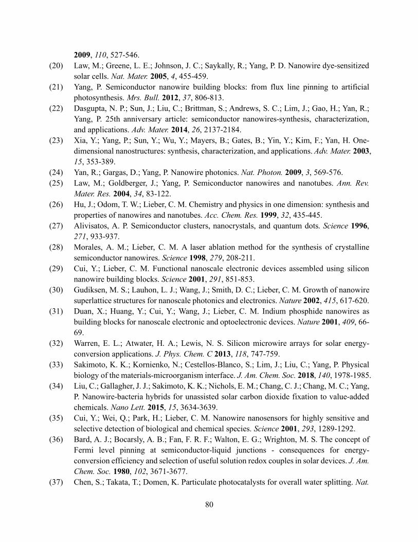
80
2009, 110, 527-546. (20) Law, M.; Greene, L. E.; Johnson, J. C.; Saykally, R.; Yang, P. D. Nanowire dye-sensitized
solar cells. Nat. Mater. 2005, 4, 455-459. (21) Yang, P. Semiconductor nanowire building blocks: from flux line pinning to artificial
photosynthesis. Mrs. Bull. 2012, 37, 806-813. (22) Dasgupta, N. P.; Sun, J.; Liu, C.; Brittman, S.; Andrews, S. C.; Lim, J.; Gao, H.; Yan, R.;
Yang, P. 25th anniversary article: semiconductor nanowires-synthesis, characterization, and applications. Adv. Mater. 2014, 26, 2137-2184.
(23) Xia, Y.; Yang, P.; Sun, Y.; Wu, Y.; Mayers, B.; Gates, B.; Yin, Y.; Kim, F.; Yan, H. One-dimensional nanostructures: synthesis, characterization, and applications. Adv. Mater. 2003, 15, 353-389.
(24) Yan, R.; Gargas, D.; Yang, P. Nanowire photonics. Nat. Photon. 2009, 3, 569-576. (25) Law, M.; Goldberger, J.; Yang, P. Semiconductor nanowires and nanotubes. Ann. Rev.
Mater. Res. 2004, 34, 83-122. (26) Hu, J.; Odom, T. W.; Lieber, C. M. Chemistry and physics in one dimension: synthesis and
properties of nanowires and nanotubes. Acc. Chem. Res. 1999, 32, 435-445. (27) Alivisatos, A. P. Semiconductor clusters, nanocrystals, and quantum dots. Science 1996,
271, 933-937. (28) Morales, A. M.; Lieber, C. M. A laser ablation method for the synthesis of crystalline
semiconductor nanowires. Science 1998, 279, 208-211. (29) Cui, Y.; Lieber, C. M. Functional nanoscale electronic devices assembled using silicon
nanowire building blocks. Science 2001, 291, 851-853. (30) Gudiksen, M. S.; Lauhon, L. J.; Wang, J.; Smith, D. C.; Lieber, C. M. Growth of nanowire
superlattice structures for nanoscale photonics and electronics. Nature 2002, 415, 617-620. (31) Duan, X.; Huang, Y.; Cui, Y.; Wang, J.; Lieber, C. M. Indium phosphide nanowires as
building blocks for nanoscale electronic and optoelectronic devices. Nature 2001, 409, 66-69.
(32) Warren, E. L.; Atwater, H. A.; Lewis, N. S. Silicon microwire arrays for solar energy-conversion applications. J. Phys. Chem. C 2013, 118, 747-759.
(33) Sakimoto, K. K.; Kornienko, N.; Cestellos-Blanco, S.; Lim, J.; Liu, C.; Yang, P. Physical biology of the materials-microorganism interface. J. Am. Chem. Soc. 2018, 140, 1978-1985.
(34) Liu, C.; Gallagher, J. J.; Sakimoto, K. K.; Nichols, E. M.; Chang, C. J.; Chang, M. C.; Yang, P. Nanowire-bacteria hybrids for unassisted solar carbon dioxide fixation to value-added chemicals. Nano Lett. 2015, 15, 3634-3639.
(35) Cui, Y.; Wei, Q.; Park, H.; Lieber, C. M. Nanowire nanosensors for highly sensitive and selective detection of biological and chemical species. Science 2001, 293, 1289-1292.
(36) Bard, A. J.; Bocarsly, A. B.; Fan, F. R. F.; Walton, E. G.; Wrighton, M. S. The concept of Fermi level pinning at semiconductor-liquid junctions - consequences for energy-conversion efficiency and selection of useful solution redox couples in solar devices. J. Am. Chem. Soc. 1980, 102, 3671-3677.
(37) Chen, S.; Takata, T.; Domen, K. Particulate photocatalysts for overall water splitting. Nat.
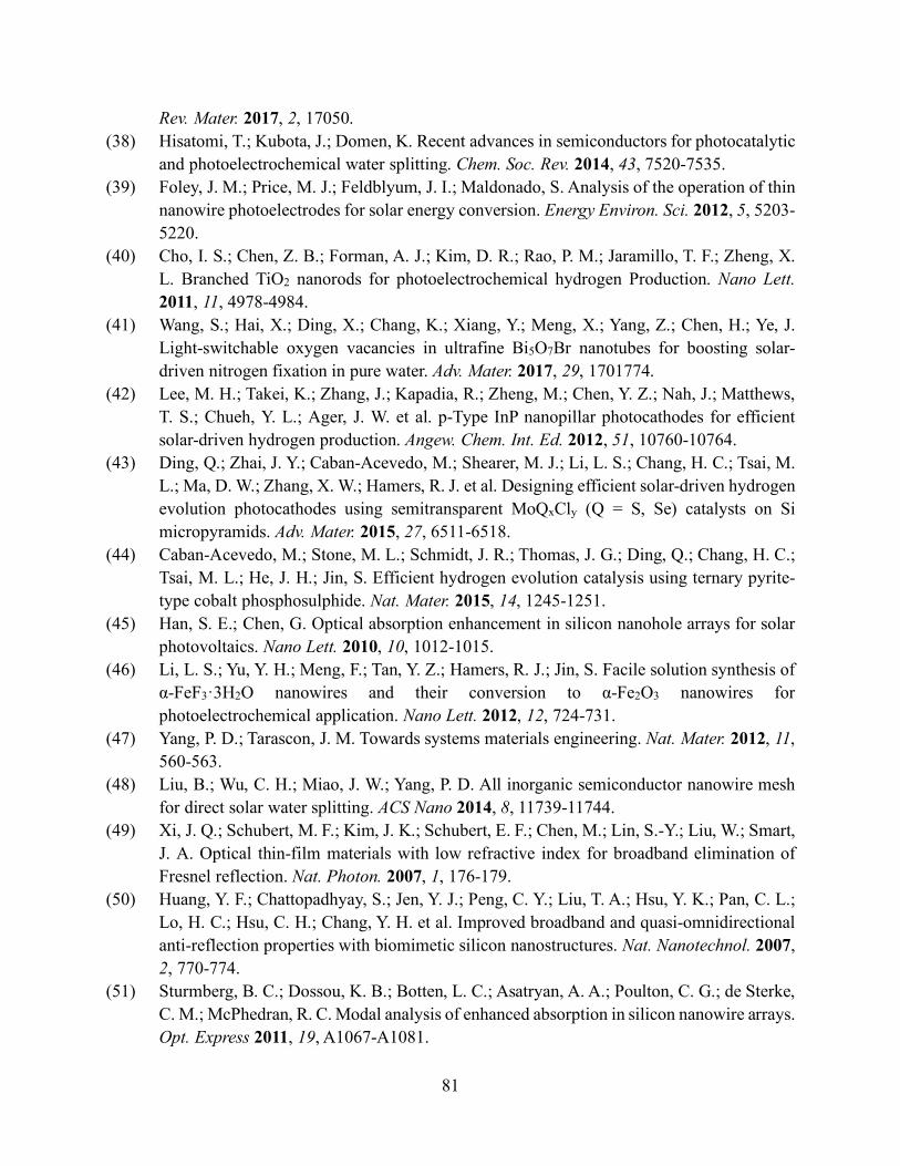
81
Rev. Mater. 2017, 2, 17050. (38) Hisatomi, T.; Kubota, J.; Domen, K. Recent advances in semiconductors for photocatalytic
and photoelectrochemical water splitting. Chem. Soc. Rev. 2014, 43, 7520-7535. (39) Foley, J. M.; Price, M. J.; Feldblyum, J. I.; Maldonado, S. Analysis of the operation of thin
nanowire photoelectrodes for solar energy conversion. Energy Environ. Sci. 2012, 5, 5203-5220.
(40) Cho, I. S.; Chen, Z. B.; Forman, A. J.; Kim, D. R.; Rao, P. M.; Jaramillo, T. F.; Zheng, X. L. Branched TiO2 nanorods for photoelectrochemical hydrogen Production. Nano Lett. 2011, 11, 4978-4984.
(41) Wang, S.; Hai, X.; Ding, X.; Chang, K.; Xiang, Y.; Meng, X.; Yang, Z.; Chen, H.; Ye, J. Light-switchable oxygen vacancies in ultrafine Bi5O7Br nanotubes for boosting solar-driven nitrogen fixation in pure water. Adv. Mater. 2017, 29, 1701774.
(42) Lee, M. H.; Takei, K.; Zhang, J.; Kapadia, R.; Zheng, M.; Chen, Y. Z.; Nah, J.; Matthews, T. S.; Chueh, Y. L.; Ager, J. W. et al. p-Type InP nanopillar photocathodes for efficient solar-driven hydrogen production. Angew. Chem. Int. Ed. 2012, 51, 10760-10764.
(43) Ding, Q.; Zhai, J. Y.; Caban-Acevedo, M.; Shearer, M. J.; Li, L. S.; Chang, H. C.; Tsai, M. L.; Ma, D. W.; Zhang, X. W.; Hamers, R. J. et al. Designing efficient solar-driven hydrogen evolution photocathodes using semitransparent MoQxCly (Q = S, Se) catalysts on Si micropyramids. Adv. Mater. 2015, 27, 6511-6518.
(44) Caban-Acevedo, M.; Stone, M. L.; Schmidt, J. R.; Thomas, J. G.; Ding, Q.; Chang, H. C.; Tsai, M. L.; He, J. H.; Jin, S. Efficient hydrogen evolution catalysis using ternary pyrite-type cobalt phosphosulphide. Nat. Mater. 2015, 14, 1245-1251.
(45) Han, S. E.; Chen, G. Optical absorption enhancement in silicon nanohole arrays for solar photovoltaics. Nano Lett. 2010, 10, 1012-1015.
(46) Li, L. S.; Yu, Y. H.; Meng, F.; Tan, Y. Z.; Hamers, R. J.; Jin, S. Facile solution synthesis of α-FeF3·3H2O nanowires and their conversion to α-Fe2O3 nanowires for photoelectrochemical application. Nano Lett. 2012, 12, 724-731.
(47) Yang, P. D.; Tarascon, J. M. Towards systems materials engineering. Nat. Mater. 2012, 11, 560-563.
(48) Liu, B.; Wu, C. H.; Miao, J. W.; Yang, P. D. All inorganic semiconductor nanowire mesh for direct solar water splitting. ACS Nano 2014, 8, 11739-11744.
(49) Xi, J. Q.; Schubert, M. F.; Kim, J. K.; Schubert, E. F.; Chen, M.; Lin, S.-Y.; Liu, W.; Smart, J. A. Optical thin-film materials with low refractive index for broadband elimination of Fresnel reflection. Nat. Photon. 2007, 1, 176-179.
(50) Huang, Y. F.; Chattopadhyay, S.; Jen, Y. J.; Peng, C. Y.; Liu, T. A.; Hsu, Y. K.; Pan, C. L.; Lo, H. C.; Hsu, C. H.; Chang, Y. H. et al. Improved broadband and quasi-omnidirectional anti-reflection properties with biomimetic silicon nanostructures. Nat. Nanotechnol. 2007, 2, 770-774.
(51) Sturmberg, B. C.; Dossou, K. B.; Botten, L. C.; Asatryan, A. A.; Poulton, C. G.; de Sterke, C. M.; McPhedran, R. C. Modal analysis of enhanced absorption in silicon nanowire arrays. Opt. Express 2011, 19, A1067-A1081.
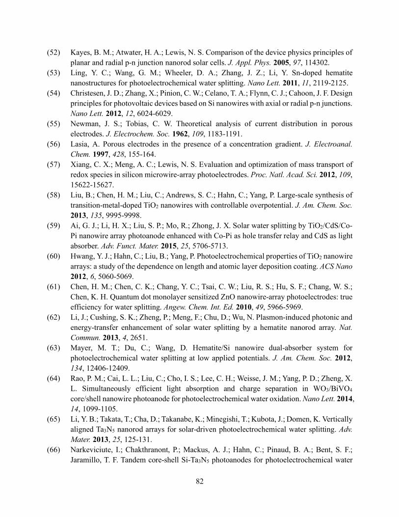
82
(52) Kayes, B. M.; Atwater, H. A.; Lewis, N. S. Comparison of the device physics principles of planar and radial p-n junction nanorod solar cells. J. Appl. Phys. 2005, 97, 114302.
(53) Ling, Y. C.; Wang, G. M.; Wheeler, D. A.; Zhang, J. Z.; Li, Y. Sn-doped hematite nanostructures for photoelectrochemical water splitting. Nano Lett. 2011, 11, 2119-2125.
(54) Christesen, J. D.; Zhang, X.; Pinion, C. W.; Celano, T. A.; Flynn, C. J.; Cahoon, J. F. Design principles for photovoltaic devices based on Si nanowires with axial or radial p-n junctions. Nano Lett. 2012, 12, 6024-6029.
(55) Newman, J. S.; Tobias, C. W. Theoretical analysis of current distribution in porous electrodes. J. Electrochem. Soc. 1962, 109, 1183-1191.
(56) Lasia, A. Porous electrodes in the presence of a concentration gradient. J. Electroanal. Chem. 1997, 428, 155-164.
(57) Xiang, C. X.; Meng, A. C.; Lewis, N. S. Evaluation and optimization of mass transport of redox species in silicon microwire-array photoelectrodes. Proc. Natl. Acad. Sci. 2012, 109, 15622-15627.
(58) Liu, B.; Chen, H. M.; Liu, C.; Andrews, S. C.; Hahn, C.; Yang, P. Large-scale synthesis of transition-metal-doped TiO2 nanowires with controllable overpotential. J. Am. Chem. Soc. 2013, 135, 9995-9998.
(59) Ai, G. J.; Li, H. X.; Liu, S. P.; Mo, R.; Zhong, J. X. Solar water splitting by TiO2/CdS/Co-Pi nanowire array photoanode enhanced with Co-Pi as hole transfer relay and CdS as light absorber. Adv. Funct. Mater. 2015, 25, 5706-5713.
(60) Hwang, Y. J.; Hahn, C.; Liu, B.; Yang, P. Photoelectrochemical properties of TiO2 nanowire arrays: a study of the dependence on length and atomic layer deposition coating. ACS Nano 2012, 6, 5060-5069.
(61) Chen, H. M.; Chen, C. K.; Chang, Y. C.; Tsai, C. W.; Liu, R. S.; Hu, S. F.; Chang, W. S.; Chen, K. H. Quantum dot monolayer sensitized ZnO nanowire-array photoelectrodes: true efficiency for water splitting. Angew. Chem. Int. Ed. 2010, 49, 5966-5969.
(62) Li, J.; Cushing, S. K.; Zheng, P.; Meng, F.; Chu, D.; Wu, N. Plasmon-induced photonic and energy-transfer enhancement of solar water splitting by a hematite nanorod array. Nat. Commun. 2013, 4, 2651.
(63) Mayer, M. T.; Du, C.; Wang, D. Hematite/Si nanowire dual-absorber system for photoelectrochemical water splitting at low applied potentials. J. Am. Chem. Soc. 2012, 134, 12406-12409.
(64) Rao, P. M.; Cai, L. L.; Liu, C.; Cho, I. S.; Lee, C. H.; Weisse, J. M.; Yang, P. D.; Zheng, X. L. Simultaneously efficient light absorption and charge separation in WO3/BiVO4 core/shell nanowire photoanode for photoelectrochemical water oxidation. Nano Lett. 2014, 14, 1099-1105.
(65) Li, Y. B.; Takata, T.; Cha, D.; Takanabe, K.; Minegishi, T.; Kubota, J.; Domen, K. Vertically aligned Ta3N5 nanorod arrays for solar-driven photoelectrochemical water splitting. Adv. Mater. 2013, 25, 125-131.
(66) Narkeviciute, I.; Chakthranont, P.; Mackus, A. J.; Hahn, C.; Pinaud, B. A.; Bent, S. F.; Jaramillo, T. F. Tandem core-shell Si-Ta3N5 photoanodes for photoelectrochemical water
83
splitting. Nano Lett. 2016, 16, 7565-7572. (67) Liu, D.; Liu, J. C.; Cai, W. Z.; Ma, J.; Yang, H. B.; Xiao, H.; Li, J.; Xiong, Y. J.; Huang, Y.
Q.; Liu, B. Selective photoelectrochemical oxidation of glycerol to high value-added dihydroxyacetone. Nat. Commun. 2019, 10, 1779.
(68) Cha, H. G.; Choi, K. S. Combined biomass valorization and hydrogen production in a photoelectrochemical cell. Nat. Chem. 2015, 7, 328-333.
(69) Oh, I.; Kye, J.; Hwang, S. Enhanced photoelectrochemical hydrogen production from silicon nanowire array photocathode. Nano Lett. 2012, 12, 298-302.
(70) Dasgupta, N. P.; Liu, C.; Andrews, S.; Prinz, F. B.; Yang, P. Atomic layer deposition of platinum catalysts on nanowire surfaces for photoelectrochemical water reduction. J. Am. Chem. Soc. 2013, 135, 12932-12935.
(71) Dai, P.; Xie, J.; Mayer, M. T.; Yang, X.; Zhan, J.; Wang, D. Solar hydrogen generation by silicon nanowires modified with platinum nanoparticle catalysts by atomic layer deposition. Angew. Chem. Int. Ed. 2013, 52, 11119-11123.
(72) Zhang, L.; Liu, C.; Wong, A. B.; Resasco, J.; Yang, P. MoS2-wrapped silicon nanowires for photoelectrochemical water reduction. Nano Res. 2014, 8, 281-287.
(73) Gao, L.; Cui, Y.; Wang, J.; Cavalli, A.; Standing, A.; Vu, T. T.; Verheijen, M. A.; Haverkort, J. E.; Bakkers, E. P.; Notten, P. H. Photoelectrochemical hydrogen production on InP nanowire arrays with molybdenum sulfide electrocatalysts. Nano Lett. 2014, 14, 3715-3719.
(74) Standing, A.; Assali, S.; Gao, L.; Verheijen, M. A.; Van Dam, D.; Cui, Y.; Notten, P. H.; Haverkort, J. E.; Bakkers, E. P. Efficient water reduction with gallium phosphide nanowires. Nat. Commun. 2015, 6, 7824.
(75) Luo, J.; Steier, L.; Son, M.-K.; Schreier, M.; Mayer, M. T.; Grätzel, M. Cu2O nanowire photocathodes for efficient and durable solar water splitting. Nano Lett. 2016, 16, 1848-1857.
(76) Huang, Q.; Kang, F.; Liu, H.; Li, Q.; Xiao, X. Highly aligned Cu2O/CuO/TiO2 core/shell nanowire arrays as photocathodes for water photoelectrolysis. J. Mater. Chem. A 2013, 1, 2418-2425.
(77) Choi, S. K.; Kang, U.; Lee, S.; Ham, D. J.; Ji, S. M.; Park, H. Sn-coupled p-Si nanowire arrays for solar formate production from CO2. Adv. Energy Mater. 2014, 4, 1301614.
(78) Liu, R.; Stephani, C.; Han, J. J.; Tan, K. L.; Wang, D. Silicon nanowires show improved performance as photocathode for catalyzed carbon dioxide photofixation. Angew. Chem. Int. Ed. 2013, 52, 4225-4228.
(79) Liu, R.; Yuan, G.; Joe, C. L.; Lightburn, T. E.; Tan, K. L.; Wang, D. Silicon nanowires as photoelectrodes for carbon dioxide fixation. Angew. Chem. Int. Ed. 2012, 124, 6813-6816.
(80) Torralba-Peñalver, E.; Luo, Y.; Compain, J.-D.; Chardon-Noblat, S.; Fabre, B. Selective catalytic electroreduction of CO2 at silicon nanowires (SiNWs) photocathodes using non-noble metal-based manganese carbonyl bipyridyl molecular catalysts in solution and grafted onto SiNWs. ACS Catal. 2015, 5, 6138-6147.
(81) Kong, Q.; Kim, D.; Liu, C.; Yu, Y.; Su, Y.; Li, Y.; Yang, P. Directed assembly of
84
nanoparticle catalysts on nanowire photoelectrodes for photoelectrochemical CO2 reduction. Nano Lett. 2016, 16, 5675-5680.
(82) Chu, S.; Fan, S.; Wang, Y.; Rossouw, D.; Wang, Y.; Botton, G. A.; Mi, Z. Tunable syngas production from CO2 and H2O in an aqueous photoelectrochemical cell. Angew. Chem. Int. Ed. 2016, 55, 14262-14266.
(83) AlOtaibi, B.; Fan, S.; Wang, D.; Ye, J.; Mi, Z. Wafer-level artificial photosynthesis for CO2
reduction into CH4 and CO using GaN nanowires. ACS Catal. 2015, 5, 5342-5348. (84) Chu, S.; Ou, P.; Ghamari, P.; Vanka, S.; Zhou, B.; Shih, I.; Song, J.; Mi, Z.
Photoelectrochemical CO2 reduction into syngas with the metal/oxide interface. J. Am. Chem. Soc. 2018, 140, 7869-7877.
(85) Ghadimkhani, G.; de Tacconi, N. R.; Chanmanee, W.; Janaky, C.; Rajeshwar, K. Efficient solar photoelectrosynthesis of methanol from carbon dioxide using hybrid CuO-Cu2O semiconductor nanorod arrays. Chem. Commun. 2013, 49, 1297-1299.
(86) Ali, M.; Zhou, F.; Chen, K.; Kotzur, C.; Xiao, C.; Bourgeois, L.; Zhang, X.; MacFarlane, D. R. Nanostructured photoelectrochemical solar cell for nitrogen reduction using plasmon-enhanced black silicon. Nat. Commun. 2016, 7, 11335.
(87) Li, L.; Wang, Y.; Vanka, S.; Mu, X.; Mi, Z.; Li, C. J. Nitrogen photofixation over III-nitride nanowires assisted by ruthenium clusters of low atomicity. Angew. Chem. Int. Ed. 2017, 56, 8701-8705.
(88) Brown, K. A.; Harris, D. F.; Wilker, M. B.; Rasmussen, A.; Khadka, N.; Hamby, H.; Keable, S.; Dukovic, G.; Peters, J. W.; Seefeldt, L. C. Light-driven dinitrogen reduction catalyzed by a CdS: nitrogenase MoFe protein biohybrid. Science 2016, 352, 448-450.
(89) Hagedorn, K.; Forgacs, C.; Collins, S.; Maldonado, S. Design considerations for nanowire heterojunctions in solar energy conversion/storage applications. J. Phys. Chem. C 2010, 114, 12010-12017.
(90) Garnett, E.; Yang, P. Light trapping in silicon nanowire solar cells. Nano Lett. 2010, 10, 1082-1087.
(91) Liu, C.; Sun, J.; Tang, J.; Yang, P. Zn-doped p-type gallium phosphide nanowire photocathodes from a surfactant-free solution synthesis. Nano Lett. 2012, 12, 5407-5411.
(92) Zhang, B. C.; Wang, H.; He, L.; Duan, C. Y.; Li, F.; Ou, X. M.; Sun, B. Q.; Zhang, X. H. The diameter-dependent photoelectrochemical performance of silicon nanowires. Chem. Commun. 2016, 52, 1369-1372.
(93) Hu, L.; Chen, G. Analysis of optical absorption in silicon nanowire arrays for photovoltaic applications. Nano Lett. 2007, 7, 3249-3252.
(94) Retamal, J. R. D.; Chen, C. Y.; Lien, D. H.; Huang, M. R. S.; Lin, C. A.; Liu, C. P.; He, J. H. Concurrent improvement in photogain and speed of a metal oxide nanowire photodetector through enhancing surface band bending via incorporating a nanoscale heterojunction. Acs Photonics 2014, 1, 354-359.
(95) Chen, M. W.; Retamal, J. R. D.; Chen, C. Y.; He, J. H. Photocarrier relaxation behavior of a single ZnO nanowire UV photodetector: effect of surface band bending. Ieee. Electr. Device. L 2012, 33, 411-413.
85
(96) Varadhan, P.; Fu, H. C.; Priante, D.; Retamal, J. R. D.; Zhao, C.; Ebaid, M.; Ng, T. K.; Ajia, I.; Mitra, S.; Roqan, I. S. et al. Surface passivation of GaN nanowires for enhanced photoelectrochemical water-splitting. Nano Lett. 2017, 17, 1520-1528.
(97) Zhao, C.; Ng, T. K.; Prabaswara, A.; Conroy, M.; Jahangir, S.; Frost, T.; O'Connell, J.; Holmes, J. D.; Parbrook, P. J.; Bhattacharya, P. et al. An enhanced surface passivation effect in InGaN/GaN disk-in-nanowire light emitting diodes for mitigating Shockley-Read-Hall recombination. Nanoscale 2015, 7, 16658-16665.
(98) Li, S. P.; Zhang, P.; Song, X. F.; Gao, L. Photoelectrochemical hydrogen production of TiO2 passivated Pt/Si-nanowire composite photocathode. Acs Appl. Mater. Interfaces 2015, 7, 18560-18565.
(99) Hu, S.; Shaner, M. R.; Beardslee, J. A.; Lichterman, M.; Brunschwig, B. S.; Lewis, N. S. Amorphous TiO2 coatings stabilize Si, GaAs, and GaP photoanodes for efficient water oxidation. Science 2014, 344, 1005-1009.
(100) Kenney, M. J.; Gong, M.; Li, Y. G.; Wu, J. Z.; Feng, J.; Lanza, M.; Dai, H. J. High-performance silicon photoanodes passivated with ultrathin nickel films for water oxidation. Science 2013, 342, 836-840.
(101) Chen, Y. W.; Prange, J. D.; Duhnen, S.; Park, Y.; Gunji, M.; Chidsey, C. E. D.; McIntyre, P. C. Atomic layer-deposited tunnel oxide stabilizes silicon photoanodes for water oxidation. Nat. Mater. 2011, 10, 539-544.
(102) Shan, B.; Vanka, S.; Li, T. T.; Troian-Gautier, L.; Brennaman, M. K.; Mi, Z. T.; Meyer, T. J. Binary molecular-semiconductor p-n junctions for photoelectrocatalytic CO2 reduction. Nat. Energy 2019, 4, 290-299.
(103) Zheng, J. Y.; Lyu, Y. H.; Wang, R. L.; Xie, C.; Zhou, H. J.; Jiang, S. P.; Wang, S. Y. Crystalline TiO2 protective layer with graded oxygen defects for efficient and stable silicon-based photocathode. Nat. Commun. 2018, 9, 3572.
(104) Dasgupta, N. P.; Yang, P. Semiconductor nanowires for photovoltaic and photoelectrochemical energy conversion. Front. Phys. 2014, 9, 289-302.
(105) Hou, W.; Cronin, S. B. A review of surface plasmon resonance-enhanced photocatalysis. Adv. Funct. Mater. 2013, 23, 1612-1619.
(106) Lee, J. B.; Choi, S.; Kim, J.; Nam, Y. S. Plasmonically-assisted nanoarchitectures for solar water splitting: obstacles and breakthroughs. Nano Today 2017, 16, 61-81.
(107) Yang, J.; Wang, D.; Han, H.; Li, C. Roles of cocatalysts in photocatalysis and photoelectrocatalysis. Acc. Chem. Res. 2013, 46, 1900-1909.
(108) O'regan, B.; Grätzel, M. A low-cost, high-efficiency solar cell based on dye-sensitized colloidal TiO2 films. Nature 1991, 353, 737-740.
(109) Youngblood, W. J.; Lee, S.-H. A.; Maeda, K.; Mallouk, T. E. Visible light water splitting using dye-sensitized oxide semiconductors. Acc. Chem. Res. 2009, 42, 1966-1973.
(110) Youngblood, W. J.; Lee, S.-H. A.; Kobayashi, Y.; Hernandez-Pagan, E. A.; Hoertz, P. G.; Moore, T. A.; Moore, A. L.; Gust, D.; Mallouk, T. E. Photoassisted overall water splitting in a visible light-absorbing dye-sensitized photoelectrochemical cell. J. Am. Chem. Soc. 2009, 131, 926-927.
86
(111) Swierk, J. R.; Mallouk, T. E. Design and development of photoanodes for water-splitting dye-sensitized photoelectrochemical cells. Chem. Soc. Rev. 2013, 42, 2357-2387.
(112) Alibabaei, L.; Sherman, B. D.; Norris, M. R.; Brennaman, M. K.; Meyer, T. J. Visible photoelectrochemical water splitting into H2 and O2 in a dye-sensitized photoelectrosynthesis cell. Proc. Natl. Acad. Sci. 2015, 112, 5899-5902.
(113) Xu, P.; Huang, T.; Huang, J.; Yan, Y.; Mallouk, T. E. Dye-sensitized photoelectrochemical water oxidation through a buried junction. Proc. Natl. Acad. Sci. 2018, 115, 6946-6951.
(114) Kibria, M. G.; Chowdhury, F. A.; Trudeau, M. L.; Guo, H.; Mi, Z. Dye-sensitized InGaN nanowire arrays for efficient hydrogen production under visible light irradiation. Nanotechnology 2015, 26, 285401.
(115) Dong, Y.-J.; Liao, J.-F.; Kong, Z.-C.; Xu, Y.-F.; Chen, Z.-J.; Chen, H.-Y.; Kuang, D.-B.; Fenske, D.; Su, C.-Y. Conformal coating of ultrathin metal-organic framework on semiconductor electrode for boosted photoelectrochemical water oxidation. Appl. Catal. B 2018, 237, 9-17.
(116) Zhang, L.; Cui, P.; Yang, H.; Chen, J.; Xiao, F.; Guo, Y.; Liu, Y.; Zhang, W.; Huo, F.; Liu, B. Metal-organic frameworks as promising photosensitizers for photoelectrochemical water splitting. Adv. Sci. 2016, 3, 1500243.
(117) Guo, C. X.; Dong, Y.; Yang, H. B.; Li, C. M. Graphene quantum dots as a green sensitizer to functionalize ZnO nanowire arrays on F-doped SnO2 glass for enhanced photoelectrochemical water splitting. Adv. Energy Mater. 2013, 3, 997-1003.
(118) Fan, W.; Chen, C.; Bai, H.; Luo, B.; Shen, H.; Shi, W. Photosensitive polymer and semiconductors bridged by Au plasmon for photoelectrochemical water splitting. Appl. Catal. B 2016, 195, 9-15.
(119) Linic, S.; Christopher, P.; Ingram, D. B. Plasmonic-metal nanostructures for efficient conversion of solar to chemical energy. Nat. Mater. 2011, 10, 911-921.
(120) Chen, H. M.; Chen, C. K.; Chen, C.-J.; Cheng, L.-C.; Wu, P. C.; Cheng, B. H.; Ho, Y. Z.; Tseng, M. L.; Hsu, Y.-Y.; Chan, T.-S. Plasmon inducing effects for enhanced photoelectrochemical water splitting: X-ray absorption approach to electronic structures. ACS Nano 2012, 6, 7362-7372.
(121) Lin, Y.-G.; Hsu, Y.-K.; Chen, Y.-C.; Wang, S.-B.; Miller, J. T.; Chen, L.-C.; Chen, K.-H. Plasmonic Ag@Ag3(PO4)1−x nanoparticle photosensitized ZnO nanorod-array photoanodes for water oxidation. Energy Environ. Sci. 2012, 5, 8917.
(122) Li, J.; Cushing, S. K.; Zheng, P.; Senty, T.; Meng, F.; Bristow, A. D.; Manivannan, A.; Wu, N. Solar hydrogen generation by a CdS-Au-TiO2 sandwich nanorod array enhanced with Au nanoparticle as electron relay and plasmonic photosensitizer. J. Am. Chem. Soc. 2014, 136, 8438-8449.
(123) Seh, Z. W.; Liu, S.; Low, M.; Zhang, S. Y.; Liu, Z.; Mlayah, A.; Han, M. Y. Janus Au-TiO2
photocatalysts with strong localization of plasmonic near-fields for efficient visible-light hydrogen generation. Adv. Mater. 2012, 24, 2310-2314.
(124) Liu, D.; Yang, D.; Gao, Y.; Ma, J.; Long, R.; Wang, C.; Xiong, Y. Flexible near-infrared photovoltaic devices based on plasmonic hot-electron injection into silicon nanowire arrays.
87
Angew. Chem. Int. Ed. 2016, 55, 4577-4581. (125) Li, S.; Zhang, J.; Kibria, M. G.; Mi, Z.; Chaker, M.; Ma, D.; Nechache, R.; Rosei, F.
Remarkably enhanced photocatalytic activity of laser ablated Au nanoparticle decorated BiFeO3 nanowires under visible-light. Chem. Commun. 2013, 49, 5856-5858.
(126) Xiao, F. X.; Hung, S. F.; Miao, J.; Wang, H. Y.; Yang, H.; Liu, B. Metal-cluster-decorated TiO2 nanotube arrays: a composite heterostructure toward versatile photocatalytic and photoelectrochemical applications. Small 2015, 11, 554-567.
(127) Xiao, F. X.; Liu, B. In situ etching-induced self-assembly of metal cluster decorated one-dimensional semiconductors for solar-powered water splitting: unraveling cooperative synergy by photoelectrochemical investigations. Nanoscale 2017, 9, 17118-17132.
(128) Pu, Y. C.; Wang, G.; Chang, K. D.; Ling, Y.; Lin, Y. K.; Fitzmorris, B. C.; Liu, C. M.; Lu, X.; Tong, Y.; Zhang, J. Z. et al. Au nanostructure-decorated TiO2 nanowires exhibiting photoactivity across entire UV-visible region for photoelectrochemical water splitting. Nano Lett. 2013, 13, 3817-3823.
(129) Wang, X.; Peng, K. Q.; Hu, Y.; Zhang, F. Q.; Hu, B.; Li, L.; Wang, M.; Meng, X. M.; Lee, S. T. Silicon/hematite core/shell nanowire array decorated with gold nanoparticles for unbiased solar water oxidation. Nano Lett. 2014, 14, 18-23.
(130) Wei, Y.; Kong, J.; Yang, L.; Ke, L.; Tan, H. R.; Liu, H.; Huang, Y.; Sun, X. W.; Lu, X.; Du, H. Polydopamine-assisted decoration of ZnO nanorods with Ag nanoparticles: an improved photoelectrochemical anode. J. Mater. Chem. A 2013, 1, 5045-5052.
(131) Wang, X.; Liow, C.; Qi, D.; Zhu, B.; Leow, W. R.; Wang, H.; Xue, C.; Chen, X.; Li, S. Programmable photo-electrochemical hydrogen evolution based on multi-segmented CdS-Au nanorod arrays. Adv. Mater. 2014, 26, 3506-3512.
(132) Shan, Z.; Clayton, D.; Pan, S.; Archana, P. S.; Gupta, A. Visible light driven photoelectrochemical properties of Ti@TiO2 nanowire electrodes sensitized with core-shell Ag@Ag2S nanoparticles. J. Phys. Chem. B 2014, 118, 14037-14046.
(133) Zhang, X.; Liu, Y.; Kang, Z. H. 3D branched ZnO nanowire arrays decorated with plasmonic Au nanoparticles for high-performance photoelectrochemical water splitting. Acs Appl. Mater. Interfaces 2014, 6, 4480-4489.
(134) Duan, C.; Wang, H.; Ou, X.; Li, F.; Zhang, X. Efficient visible light photocatalyst fabricated by depositing plasmonic Ag nanoparticles on conductive polymer-protected Si nanowire arrays for photoelectrochemical hydrogen generation. ACS Appl. Mater. Interfaces 2014, 6, 9742-9750.
(135) DuChene, J. S.; Williams, B. P.; Johnston-Peck, A. C.; Qiu, J.; Gomes, M.; Amilhau, M.; Bejleri, D.; Weng, J.; Su, D.; Huo, F. et al. Elucidating the sole contribution from electromagnetic near-fields in plasmon-enhanced Cu2O photocathodes. Adv. Energy Mater. 2016, 6, 1501250.
(136) Liu, Y.; Gu, Y.; Yan, X.; Kang, Z.; Lu, S.; Sun, Y.; Zhang, Y. Design of sandwich-structured ZnO/ZnS/Au photoanode for enhanced efficiency of photoelectrochemical water splitting. Nano Res. 2015, 8, 2891-2900.
(137) Wang, Y.; Fan, S.; AlOtaibi, B.; Wang, Y.; Li, L.; Mi, Z. A monolithically integrated
88
gallium nitride nanowire/silicon solar cell photocathode for selective carbon dioxide reduction to methane. Chem. Eur. J. 2016, 22, 8809-8813.
(138) Yang, X.; Li, H.; Zhang, W.; Sun, M.; Li, L.; Xu, N.; Wu, J.; Sun, J. High visible photoelectrochemical activity of Ag nanoparticle-sandwiched CdS/Ag/ZnO nanorods. ACS Appl. Mater. Interfaces 2017, 9, 658-667.
(139) Liu, Y.; Yan, X.; Kang, Z.; Li, Y.; Shen, Y.; Sun, Y.; Wang, L.; Zhang, Y. Synergistic effect of surface plasmonic particles and surface passivation layer on ZnO nanorods array for improved photoelectrochemical water splitting. Sci. Rep. 2016, 6, 29907.
(140) Li, H.; Li, Z.; Yu, Y.; Ma, Y.; Yang, W.; Wang, F.; Yin, X.; Wang, X. Surface-plasmon-resonance-enhanced photoelectrochemical water splitting from au-nanoparticle-decorated 3D TiO2 nanorod architectures. J. Phys. Chem. C 2017, 121, 12071-12079.
(141) Kim, S.; Yu, Y.; Jeong, S. Y.; Lee, M. G.; Jeong, H. W.; Kwon, Y. M.; Baik, J. M.; Park, H.; Jang, H. W.; Lee, S. Plasmonic gold nanoparticle-decorated BiVO4/ZnO nanowire heterostructure photoanodes for efficient water oxidation. Catal. Sci. Technol. 2018, 8, 3759-3766.
(142) Wang, L.; Wang, Y.; Schmuki, P.; Kment, S.; Zboril, R. Nanostar morphology of plasmonic particles strongly enhances photoelectrochemical water splitting of TiO2 nanorods with superior incident photon-to-current conversion efficiency in visible/near-infrared region. Electrochim. Acta 2018, 260, 212-220.
(143) Wang, C.-C.; Chou, P.-H.; Yu, Y.-H.; Kei, C.-C. Deposition of Ni nanoparticles on black TiO2 nanowire arrays for photoelectrochemical water splitting by atomic layer deposition. Electrochim. Acta 2018, 284, 211-219.
(144) Kumar, D.; Singh, S.; Khare, N. Plasmonic Ag nanoparticles decorated NaNbO3 nanorods for efficient photoelectrochemical water splitting. Int. J. Hydrogen Energy 2018, 43, 8198-8205.
(145) Li, C.; Wang, P.; Li, H.; Wang, M.; Zhang, J.; Qi, G.; Jin, Y. Plasmon-driven water splitting enhancement on plasmonic metal-insulator-semiconductor hetero-nanostructures: unraveling the crucial role of interfacial engineering. Nanoscale 2018, 10, 14290-14297.
(146) Liu, D.; Ma, J.; Long, R.; Gao, C.; Xiong, Y. Silicon nanostructures for solar-driven catalytic applications. Nano Today 2017, 17, 96-116.
(147) Roger, I.; Shipman, M. A.; Symes, M. D. Earth-abundant catalysts for electrochemical and photoelectrochemical water splitting. Nat. Rev. Chem. 2017, 1, 0003.
(148) Bai, S.; Jiang, J.; Zhang, Q.; Xiong, Y. Steering charge kinetics in photocatalysis: intersection of materials syntheses, characterization techniques and theoretical simulations. Chem. Soc. Rev. 2015, 44, 2893-2939.
(149) Cao, S.; Yan, X.; Kang, Z.; Liang, Q.; Liao, X.; Zhang, Y. Band alignment engineering for improved performance and stability of ZnFe2O4 modified CdS/ZnO nanostructured photoanode for PEC water splitting. Nano Energy 2016, 24, 25-31.
(150) Yang, H. B.; Miao, J.; Hung, S.-F.; Huo, F.; Chen, H. M.; Liu, B. Stable quantum dot photoelectrolysis cell for unassisted visible light solar water splitting. ACS Nano 2014, 8, 10403-10413.
89
(151) Hensel, J.; Wang, G.; Li, Y.; Zhang, J. Z. Synergistic effect of CdSe quantum dot sensitization and nitrogen doping of TiO2 nanostructures for photoelectrochemical solar hydrogen generation. Nano Lett. 2010, 10, 478-483.
(152) AlOtaibi, B.; Kong, X.; Vanka, S.; Woo, S. Y.; Pofelski, A.; Oudjedi, F.; Fan, S.; Kibria, M. G.; Botton, G. A.; Ji, W. et al. Photochemical carbon dioxide reduction on Mg-doped Ga(In)N nanowire arrays under visible light irradiation. ACS Energy Lett. 2016, 1, 246-252.
(153) Kibria, M. G.; Chowdhury, F. A.; Zhao, S.; AlOtaibi, B.; Trudeau, M. L.; Guo, H.; Mi, Z. Visible light-driven efficient overall water splitting using p-type metal-nitride nanowire arrays. Nat. Commun. 2015, 6, 6797.
(154) Wang, G.; Yang, X.; Qian, F.; Zhang, J. Z.; Li, Y. Double-sided CdS and CdSe quantum dot co-sensitized ZnO nanowire arrays for photoelectrochemical hydrogen generation. Nano Lett. 2010, 10, 1088-1092.
(155) Wang, H.; Bai, Y.; Zhang, H.; Zhang, Z.; Li, J.; Guo, L. CdS quantum dots-sensitized TiO2
nanorod array on transparent conductive glass photoelectrodes. J. Phys. Chem. C 2010, 114, 16451-16455.
(156) Wang, H.; Wang, G.; Ling, Y.; Lepert, M.; Wang, C.; Zhang, J. Z.; Li, Y. Photoelectrochemical study of oxygen deficient TiO2 nanowire arrays with CdS quantum dot sensitization. Nanoscale 2012, 4, 1463-1466.
(157) Wu, G.; Tian, M.; Chen, A. Synthesis of CdS quantum-dot sensitized TiO2 nanowires with high photocatalytic activity for water splitting. J. Photoch. Photobio A 2012, 233, 65-71.
(158) Seol, M.; Jang, J.-W.; Cho, S.; Lee, J. S.; Yong, K. Highly efficient and stable cadmium chalcogenide quantum dot/ZnO nanowires for photoelectrochemical hydrogen generation. Chem. Mater. 2012, 25, 184-189.
(159) Shi, X.; Choi, I. Y.; Zhang, K.; Kwon, J.; Kim, D. Y.; Lee, J. K.; Oh, S. H.; Kim, J. K.; Park, J. H. Efficient photoelectrochemical hydrogen production from bismuth vanadate-decorated tungsten trioxide helix nanostructures. Nat. Commun. 2014, 5, 4775.
(160) Xiao, F. X.; Miao, J.; Wang, H. Y.; Yang, H.; Chen, J.; Liu, B. Electrochemical construction of hierarchically ordered CdSe-sensitized TiO2 nanotube arrays: towards versatile photoelectrochemical water splitting and photoredox applications. Nanoscale 2014, 6, 6727-6237.
(161) Peng, Z.; Liu, Y.; Zhao, Y.; Chen, K.; Kovalev, V.; Chen, W. Photoelectrochemical behavior of TiO2 nanorod arrays decorated with CuInS2 quantum dots. Appl. Surf. Sci. 2014, 292, 514-519.
(162) Guo, C. X.; Xie, J.; Yang, H.; Li, C. M. Au@CdS core-shell nanoparticles-modified ZnO nanowires photoanode for efficient photoelectrochemical water splitting. Adv. Sci. 2015, 2, 1500135.
(163) Jin, B.; Jiao, Z.; Bi, Y. Efficient charge separation between Bi2MoO6 nanosheets and ZnO nanowires for enhanced photoelectrochemical properties. J. Mater. Chem. A 2015, 3, 19702-19705.
(164) Ning, F.; Shao, M.; Xu, S.; Fu, Y.; Zhang, R.; Wei, M.; Evans, D. G.; Duan, X.
90
TiO2/graphene/NiFe-layered double hydroxide nanorod array photoanodes for efficient photoelectrochemical water splitting. Energy Environ. Sci. 2016, 9, 2633-2643.
(165) Zheng, X. L.; Dinh, C. T.; de Arquer, F. P.; Zhang, B.; Liu, M.; Voznyy, O.; Li, Y. Y.; Knight, G.; Hoogland, S.; Lu, Z. H. et al. ZnFe2O4 leaves grown on TiO2 trees enhance photoelectrochemical water splitting. Small 2016, 12, 3181-3188.
(166) An, T.; Tang, J.; Zhang, Y.; Quan, Y.; Gong, X.; Al-Enizi, A. M.; Elzatahry, A. A.; Zhang, L.; Zheng, G. Photoelectrochemical conversion from graphitic C3N4 quantum dot decorated semiconductor nanowires. ACS Appl. Mater. Interfaces 2016, 8, 12772-12779.
(167) Mao, C.; Wang, Y.; Jiao, W.; Chen, X.; Lin, Q.; Deng, M.; Ling, Y.; Zhou, Y.; Bu, X.; Feng, P. Integrating zeolite-type chalcogenide with titanium dioxide nanowires for enhanced photoelectrochemical activity. Langmuir 2017, 33, 13634-13639.
(168) Pi, Y.; Li, Z.; Xu, D.; Liu, J.; Li, Y.; Zhang, F.; Zhang, G.; Peng, W.; Fan, X. 1T-phase MoS2 nanosheets on TiO2 nanorod arrays: 3D photoanode with extraordinary catalytic performance. ACS Sustainable Chem. Eng. 2017, 5, 5175-5182.
(169) Wang, M.; Han, K.; Zhang, S.; Sun, L. Integration of organometallic complexes with semiconductors and other nanomaterials for photocatalytic H2 production. Coord. Chem. Rev. 2015, 287, 1-14.
(170) Hou, Y.; Abrams, B. L.; Vesborg, P. C.; Bjorketun, M. E.; Herbst, K.; Bech, L.; Setti, A. M.; Damsgaard, C. D.; Pedersen, T.; Hansen, O. et al. Bioinspired molecular co-catalysts bonded to a silicon photocathode for solar hydrogen evolution. Nat. Mater. 2011, 10, 434-438.
(171) Jiang, D.; Irfan, R. M.; Sun, Z.; Lu, D.; Du, P. Synergistic effect of a molecular cocatalyst and a heterojunction in a 1D semiconductor photocatalyst for robust and highly efficient solar hydrogen production. ChemSusChem 2016, 9, 3084-3092.
(172) Hou, Y.; Zhu, Z.; Xu, Y.; Guo, F.; Zhang, J.; Wang, X. Efficient photoelectrochemical hydrogen production over p-Si nanowire arrays coupled with molybdenum–sulfur clusters. Int. J. Hydrogen Energy 2017, 42, 2832-2838.
(173) Mange, Y. J.; Chandrasekaran, S.; Hollingsworth, N.; Voelcker, N. H.; Parkin, I. P.; Nann, T.; Macdonald, T. J. {Ni4O4} cluster complex to enhance the reductive photocurrent response on silicon nanowire photocathodes. Nanomaterials 2017, 7, 33.
(174) Jin, T.; He, D.; Li, W.; Stanton, C. J.; Pantovich, S. A.; Majetich, G. F.; Schaefer, H. F.; Agarwal, J.; Wang, D.; Li, G. CO2 reduction with Re(i)-NHC compounds: driving selective catalysis with a silicon nanowire photoelectrode. Chem. Commun. 2016, 52, 14258-14261.
(175) Seh, Z. W.; Kibsgaard, J.; Dickens, C. F.; Chorkendorff, I.; Norskov, J. K.; Jaramillo, T. F. Combining theory and experiment in electrocatalysis: insights into materials design. Science 2017, 355, eaad4998.
(176) Chen, J. G.; Crooks, R. M.; Seefeldt, L. C.; Bren, K. L.; Bullock, R. M.; Darensbourg, M. Y.; Holland, P. L.; Hoffman, B.; Janik, M. J.; Jones, A. K. et al. Beyond fossil fuel-driven nitrogen transformations. Science 2018, 360, eaar6611.
(177) Han, H. X.; Shi, C.; Zhang, N.; Yuan, L.; Sheng, G. P. Visible-light-enhanced Cr(VI) reduction at Pd-decorated silicon nanowire photocathode in photoelectrocatalytic
91
microbial fuel cell. Sci. Total. Environ. 2018, 639, 1512-1519. (178) Sun, J.; Liu, C.; Yang, P. Surfactant-free, large-scale, solution-liquid-solid growth of
gallium phosphide nanowires and their use for visible-light-driven hydrogen production from water reduction. J. Am. Chem. Soc. 2011, 133, 19306-19309.
(179) Qiu, J.; Zeng, G.; Ha, M. A.; Ge, M.; Lin, Y.; Hettick, M.; Hou, B.; Alexandrova, A. N.; Javey, A.; Cronin, S. B. Artificial photosynthesis on TiO2-passivated InP nanopillars. Nano Lett. 2015, 15, 6177-6181.
(180) Sun, K.; Pang, X.; Shen, S.; Qian, X.; Cheung, J. S.; Wang, D. Metal oxide composite enabled nanotextured Si photoanode for efficient solar driven water oxidation. Nano Lett. 2013, 13, 2064-2072.
(181) Hu, D.; Xiang, J.; Zhou, Q.; Su, S.; Zhang, Z.; Wang, X.; Jin, M.; Nian, L.; Nozel, R.; Zhou, G. et al. One-step chemical vapor deposition of MoS2 nanosheets on SiNWs as photocathodes for efficient and stable solar-driven hydrogen production. Nanoscale 2018, 10, 3518-3525.
(182) Tran, P. D.; Pramana, S. S.; Kale, V. S.; Nguyen, M.; Chiam, S. Y.; Batabyal, S. K.; Wong, L. H.; Barber, J.; Loo, J. Novel assembly of an MoS2 electrocatalyst onto a silicon nanowire array electrode to construct a photocathode composed of elements abundant on the earth for hydrogen generation. Chem. Eur. J 2012, 18, 13994-13999.
(183) Long, L.-L.; Zhang, A.-Y.; Huang, Y.-X.; Zhang, X.; Yu, H.-Q. A robust cocatalyst Pd4S uniformly anchored onto Bi2S3 nanorods for enhanced visible light photocatalysis. J. Mater. Chem. A 2015, 3, 4301-4306.
(184) Zhang, H.; Ding, Q.; He, D.; Liu, H.; Liu, W.; Li, Z.; Yang, B.; Zhang, X.; Lei, L.; Jin, S. A p-Si/NiCoSex core/shell nanopillar array photocathode for enhanced photoelectrochemical hydrogen production. Energy Environ. Sci. 2016, 9, 3113-3119.
(185) Bao, X. Q.; Fatima Cerqueira, M.; Alpuim, P.; Liu, L. Silicon nanowire arrays coupled with cobalt phosphide spheres as low-cost photocathodes for efficient solar hydrogen evolution. Chem. Commun. 2015, 51, 10742-10745.
(186) Huang, Z.; Chen, Z.; Chen, Z.; Lv, C.; Meng, H.; Zhang, C. Ni12P5 nanoparticles as an efficient catalyst for hydrogen generation via electrolysis and photoelectrolysis. ACS Nano 2014, 8, 8121-8129.
(187) Ai, G.; Mo, R.; Li, H.; Zhong, J. Cobalt phosphate modified TiO2 nanowire arrays as co-catalysts for solar water splitting. Nanoscale 2015, 7, 6722-6728.
(188) Lv, C.; Chen, Z.; Chen, Z.; Zhang, B.; Qin, Y.; Huang, Z.; Zhang, C. Silicon nanowires loaded with iron phosphide for effective solar-driven hydrogen production. J. Mater. Chem. A 2015, 3, 17669-17675.
(189) Weng, B.; Wei, W.; Yiliguma, Y.; Wu, H.; Alenizi, A. M.; Zheng, G. Bifunctional CoP and CoN porous nanocatalysts derived from ZIF-67 in situ grown on nanowire photoelectrodes for efficient photoelectrochemical water splitting and CO2 reduction. J. Mater. Chem. A 2016, 4, 15353-15360.
(190) Yang, Y.; Wang, M.; Zhang, P.; Wang, W.; Han, H.; Sun, L. Evident enhancement of photoelectrochemical hydrogen production by electroless deposition of M-B (M = Ni, Co)
92
catalysts on silicon nanowire arrays. ACS Appl. Mater. Interfaces 2016, 8, 30143-30151. (191) Zhang, R.; Shao, M.; Xu, S.; Ning, F.; Zhou, L.; Wei, M. Photo-assisted synthesis of zinc-
iron layered double hydroxides/TiO2 nanoarrays toward highly-efficient photoelectrochemical water splitting. Nano Energy 2017, 33, 21-28.
(192) Sim, U.; Moon, J.; An, J.; Kang, J. H.; Jerng, S. E.; Moon, J.; Cho, S.-P.; Hong, B. H.; Nam, K. T. N-doped graphene quantum sheets on silicon nanowire photocathodes for hydrogen production. Energy Environ. Sci. 2015, 8, 1329-1338.
(193) Yang, K. D.; Ha, Y.; Sim, U.; An, J.; Lee, C. W.; Jin, K.; Kim, Y.; Park, J.; Hong, J. S.; Lee, J. H. et al. Graphene quantum sheet catalyzed silicon photocathode for selective CO2
conversion to CO. Adv. Funct. Mater. 2016, 26, 233-242. (194) Jin, J.; Yu, J.; Liu, G.; Wong, P. K. Single crystal CdS nanowires with high visible-light
photocatalytic H2-production performance. J. Mater. Chem. A 2013, 1, 10927-10934. (195) Shen, M.; Yan, Z.; Yang, L.; Du, P.; Zhang, J.; Xiang, B. MoS2 nanosheet/TiO2 nanowire
hybrid nanostructures for enhanced visible-light photocatalytic activities. Chem. Commun. 2014, 50, 15447-15449.
(196) Dai, D.; Xu, H.; Ge, L.; Han, C.; Gao, Y.; Li, S.; Lu, Y. In-situ synthesis of CoP co-catalyst decorated Zn0.5Cd0.5S photocatalysts with enhanced photocatalytic hydrogen production activity under visible light irradiation. Appl. Catal. B 2017, 217, 429-436.
(197) Jang, J. S.; Joshi, U. A.; Lee, J. S. Solvothermal synthesis of CdS nanowires for photocatalytic hydrogen and electricity production. J. Phys. Chem. C 2007, 111, 13280-13287.
(198) Zhou, W.; Guan, Y.; Wang, D.; Zhang, X.; Liu, D.; Jiang, H.; Wang, J.; Liu, X.; Liu, H.; Chen, S. PdO/TiO2 and Pd/TiO2 heterostructured nanobelts with enhanced photocatalytic activity. Chem. Asian J. 2014, 9, 1648-1654.
(199) Xu, L.; Zhao, Y.; Owusu, K. A.; Zhuang, Z.; Liu, Q.; Wang, Z.; Li, Z.; Mai, L. Recent advances in nanowire-biosystem interfaces: from chemical conversion, energy production to electrophysiology. Chem 2018, 4, 1538-1559.
(200) Sakimoto, K. K.; Kornienko, N.; Yang, P. Cyborgian material design for solar fuel production: the emerging photosynthetic biohybrid systems. Acc. Chem. Res. 2017, 50, 476-481.
(201) Jeong, H. E.; Kim, I.; Karam, P.; Choi, H. J.; Yang, P. Bacterial recognition of silicon nanowire arrays. Nano Lett. 2013, 13, 2864-2869.
(202) Sakimoto, K. K.; Liu, C.; Lim, J.; Yang, P. Salt-induced self-assembly of bacteria on nanowire arrays. Nano Lett. 2014, 14, 5471-5476.
(203) Nevin, K. P.; Woodard, T. L.; Franks, A. E.; Summers, Z. M.; Lovley, D. R. Microbial electrosynthesis: feeding microbes electricity to convert carbon dioxide and water to multicarbon extracellular organic compounds. Mbio 2010, 1, e00103-10.
(204) Drake, H. L.; Gossner, A. S.; Daniel, S. L. Old acetogens, new light. Ann. N. Y. Acda. Sci. 2008, 1125, 100-128.
(205) Tang, J.; Zhang, Y. Y.; Kong, B.; Wang, Y. C.; Da, P. M.; Li, J.; Elzatahry, A. A.; Zhao, D. Y.; Gong, X. G.; Zheng, G. F. Solar-driven photoelectrochemical probing of
93
nanodot/nanowire/cell interface. Nano Lett. 2014, 14, 2702-2708. (206) Zhu, Y. C.; Wang, Q.; Zhang, L. B.; Zhao, W. W.; Xu, J. J.; Chen, H. Y.
Photoelectrochemical probing of cellular interfaces and evaluation of cellular H2S production based on in situ-generated CdS-enhanced TiO2 nanotube heterostructures. Chemelectrochem 2017, 4, 1011-1015.
(207) Parameswaran, R.; Carvalho-de-Souza, J. L.; Jiang, Y. W.; Burke, M. J.; Zimmerman, J. F.; Koehler, K.; Phillips, A. W.; Yi, J.; Adams, E. J.; Bezanilla, F. et al. Photoelectrochemical modulation of neuronal activity with free-standing coaxial silicon nanowires. Nat. Nanotechnol. 2018, 13, 260-266.
(208) Doyle, R. L.; Lyons, M. E. The oxygen evolution reaction: mechanistic concepts and catalyst design. In Photoelectrochemical solar fuel production. 2016, 41-104.
(209) Dau, H.; Limberg, C.; Reier, T.; Risch, M.; Roggan, S.; Strasser, P. The mechanism of water oxidation: from electrolysis via homogeneous to biological catalysis. ChemCatChem 2010, 2, 724-761.
(210) Man, I. C.; Su, H.-Y.; Calle-Vallejo, F.; Hansen, H. A.; Martínez, J. I.; Inoglu, N. G.; Kitchin, J.; Jaramillo, T. F.; Nørskov, J. K.; Rossmeisl, J. Universality in oxygen evolution electrocatalysis on oxide surfaces. ChemCatChem 2011, 3, 1159-1165.
(211) Wang, H. Y.; Hung, S. F.; Chen, H. Y.; Chan, T. S.; Chen, H. M.; Liu, B. In operando identification of geometrical-site-dependent water oxidation activity of spinel Co3O4. J. Am. Chem. Soc. 2016, 138, 36-39.
(212) Wang, H. Y.; Hung, S. F.; Hsu, Y. Y.; Zhang, L.; Miao, J.; Chan, T. S.; Xiong, Q.; Liu, B. In situ spectroscopic identification of µ-OO bridging on spinel Co3O4 water oxidation electrocatalyst. J. Phys. Chem. Lett. 2016, 7, 4847-4853.
(213) Li, X.; Wang, H.-Y.; Yang, H.; Cai, W.; Liu, S.; Liu, B. In situ/operando characterization techniques to probe the electrochemical reactions for energy conversion. Small Methods 2018, 2, 1700395.
(214) Zandi, O.; Hamann, T. W. Determination of photoelectrochemical water oxidation intermediates on haematite electrode surfaces using operando infrared spectroscopy. Nat. Chem. 2016, 8, 778-783.
(215) Valdes, A.; Qu, Z.-W.; Kroes, G.-J.; Rossmeisl, J.; Nørskov, J. K. Oxidation and photo-oxidation of water on TiO2 surface. J. Phys. Chem. C 2008, 112, 9872-9879.
(216) Tao, H. B.; Fang, L.; Chen, J.; Yang, H. B.; Gao, J.; Miao, J.; Chen, S.; Liu, B. Identification of surface reactivity descriptor for transition metal oxides in oxygen evolution reaction. J. Am. Chem. Soc. 2016, 138, 9978-9985.
(217) Fujishima, A.; Honda, K. Electrochemical photolysis of water at a semiconductor electrode. Nature 1972, 238, 37-38.
(218) Shankar, K.; Basham, J. I.; Allam, N. K.; Varghese, O. K.; Mor, G. K.; Feng, X.; Paulose, M.; Seabold, J. A.; Choi, K.-S.; Grimes, C. A. Recent advances in the use of TiO2 nanotube and nanowire arrays for oxidative photoelectrochemistry. J. Phys. Chem. C 2009, 113, 6327-6359.
(219) Kelzenberg, M. D.; Boettcher, S. W.; Petykiewicz, J. A.; Turner-Evans, D. B.; Putnam, M.
94
C.; Warren, E. L.; Spurgeon, J. M.; Briggs, R. M.; Lewis, N. S.; Atwater, H. A. Enhanced absorption and carrier collection in Si wire arrays for photovoltaic applications. Nat. Mater. 2010, 9, 239-244.
(220) Palmisano, G.; Garcia-Lopez, E.; Marci, G.; Loddo, V.; Yurdakal, S.; Augugliaro, V.; Palmisano, L. Advances in selective conversions by heterogeneous photocatalysis. Chem. Commun. 2010, 46, 7074-7089.
(221) Hidaka, H.; Nagaoka, H.; Nohara, K.; Shimura, T.; Horikoshi, S.; Zhao, J.; Serpone, N. A mechanistic study of the photoelectrochemical oxidation of organic compounds on a TiO2/TCO particulate film electrode assembly. J. Photoch. Photobio., A 1996, 98, 73-78.
(222) He, C.; Xiong, Y.; Chen, J.; Zha, C.; Zhu, X. Photoelectrochemical performance of Ag–TiO2/ITO film and photoelectrocatalytic activity towards the oxidation of organic pollutants. J. Photoch. Photobio., A 2003, 157, 71-79.
(223) Mesa, C. A.; Kafizas, A.; Francas, L.; Pendlebury, S. R.; Pastor, E.; Ma, Y.; Le Formal, F.; Mayer, M. T.; Gratzel, M.; Durrant, J. R. Kinetics of photoelectrochemical oxidation of methanol on hematite photoanodes. J. Am. Chem. Soc. 2017, 139, 11537-11543.
(224) You, B.; Jiang, N.; Liu, X.; Sun, Y. Simultaneous H2 generation and biomass upgrading in water by an efficient noble-metal-free bifunctional electrocatalyst. Angew. Chem. Int. Ed. 2016, 55, 9913-9917.
(225) Han, G.; Jin, Y. H.; Burgess, R. A.; Dickenson, N. E.; Cao, X. M.; Sun, Y. Visible-light-driven valorization of biomass intermediates integrated with H2 production catalyzed by ultrathin Ni/CdS nanosheets. J. Am. Chem. Soc. 2017, 139, 15584-15587.
(226) Zhang, L.; Chen, R.; Luo, J.; Miao, J.; Gao, J.; Liu, B. Sustainable hydrogen and chemical production via photo-electrochemical reforming of biomass-derived alcohols. Nano Res. 2016, 9, 3388-3393.
(227) White, J. L.; Baruch, M. F.; Pander III, J. E.; Hu, Y.; Fortmeyer, I. C.; Park, J. E.; Zhang, T.; Liao, K.; Gu, J.; Yan, Y. Light-driven heterogeneous reduction of carbon dioxide: photocatalysts and photoelectrodes. Chem. Rev. 2015, 115, 12888-12935.
(228) Chen, X.; Li, N.; Kong, Z.; Ong, W.-J.; Zhao, X. Photocatalytic fixation of nitrogen to ammonia: state-of-the-art advancements and future prospects. Mater. Horiz. 2018, 5, 9-27.
(229) Zhang, N.; Long, R.; Gao, C.; Xiong, Y. Recent progress on advanced design for photoelectrochemical reduction of CO2 to fuels. Sci. China Mater. 2018, 61, 771-805.
(230) Huang, Q.; Ye, Z.; Xiao, X. Recent progress in photocathodes for hydrogen evolution. J. Mater. Chem. A 2015, 3, 15824-15837.
(231) Boettcher, S. W.; Spurgeon, J. M.; Putnam, M. C.; Warren, E. L.; Turner-Evans, D. B.; Kelzenberg, M. D.; Maiolo, J. R.; Atwater, H. A.; Lewis, N. S. Energy-conversion properties of vapor-liquid-solid–grown silicon wire-array photocathodes. Science 2010, 327, 185-187.
(232) Goodey, A. P.; Eichfeld, S. M.; Lew, K.-K.; Redwing, J. M.; Mallouk, T. E. Silicon nanowire array photoelectrochemical cells. J. Am. Chem. Soc. 2007, 129, 12344-12345.
(233) Fan, S.; AlOtaibi, B.; Woo, S. Y.; Wang, Y.; Botton, G. A.; Mi, Z. High efficiency solar-to-hydrogen conversion on a monolithically integrated InGaN/GaN/Si adaptive tunnel
95
junction photocathode. Nano Lett. 2015, 15, 2721-2726. (234) Appel, A. M.; Bercaw, J. E.; Bocarsly, A. B.; Dobbek, H.; DuBois, D. L.; Dupuis, M.; Ferry,
J. G.; Fujita, E.; Hille, R.; Kenis, P. J. Frontiers, opportunities, and challenges in biochemical and chemical catalysis of CO2 fixation. Chem. Rev. 2013, 113, 6621-6658.
(235) Kumar, B.; Llorente, M.; Froehlich, J.; Dang, T.; Sathrum, A.; Kubiak, C. P. Photochemical and photoelectrochemical reduction of CO2. Annu. Rev. Phys. Chem. 2012, 63, 541-569.
(236) Kim, D.; Resasco, J.; Yu, Y.; Asiri, A. M.; Yang, P. Synergistic geometric and electronic effects for electrochemical reduction of carbon dioxide using gold–copper bimetallic nanoparticles. Nat. Commun. 2014, 5, 4948.
(237) Kuhl, K. P.; Hatsukade, T.; Cave, E. R.; Abram, D. N.; Kibsgaard, J.; Jaramillo, T. F. Electrocatalytic conversion of carbon dioxide to methane and methanol on transition metal surfaces. J. Am. Chem. Soc. 2014, 136, 14107-14113.
(238) Skulason, E.; Bligaard, T.; Gudmundsdottir, S.; Studt, F.; Rossmeisl, J.; Abild-Pedersen, F.; Vegge, T.; Jonsson, H.; Norskov, J. K. A theoretical evaluation of possible transition metal electro-catalysts for N2 reduction. Phys. Chem. Chem. Phys. 2012, 14, 1235-1245.
(239) Montoya, J. H.; Tsai, C.; Vojvodic, A.; Norskov, J. K. The challenge of electrochemical ammonia synthesis: a new perspective on the role of nitrogen scaling relations. ChemSusChem 2015, 8, 2180-2186.
(240) Zhao, W.; Xi, H.; Zhang, M.; Li, Y.; Chen, J.; Zhang, J.; Zhu, X. Enhanced quantum yield of nitrogen fixation for hydrogen storage with in situ-formed carbonaceous radicals. Chem. Commun. 2015, 51, 4785-4788.
(241) Hwang, Y. J.; Boukai, A.; Yang, P. High density n-Si/n-TiO2 core/shell nanowire arrays with enhanced photoactivity. Nano Lett. 2008, 9, 410-415.
(242) Hwang, Y. J.; Wu, C. H.; Hahn, C.; Jeong, H. E.; Yang, P. Si/InGaN core/shell hierarchical nanowire arrays and their photoelectrochemical properties. Nano Lett. 2012, 12, 1678-1682.
(243) Fountaine, K. T.; Whitney, W. S.; Atwater, H. A. Resonant absorption in semiconductor nanowires and nanowire arrays: relating leaky waveguide modes to Bloch photonic crystal modes. J. Appl. Phys. 2014, 116, 153106.
(244) Tachikawa, T.; Majima, T. Single-molecule, single-particle fluorescence imaging of TiO2-based photocatalytic reactions. Chem. Soc. Rev. 2010, 39, 4802-4819.
(245) Hesari, M.; Mao, X.; Chen, P. Charge carrier activity on single-particle photo(electro)catalysts: toward function in solar energy conversion. J. Am. Chem. Soc. 2018, 140, 6729-6740.
(246) Yan, R.; Park, J. H.; Choi, Y.; Heo, C. J.; Yang, S. M.; Lee, L. P.; Yang, P. Nanowire-based single-cell endoscopy. Nat. Nanotechnol. 2011, 7, 191-196.
(247) Tian, B.; Kempa, T. J.; Lieber, C. M. Single nanowire photovoltaics. Chem. Soc. Rev. 2009, 38, 16-24.
(248) Tang, J.; Huo, Z.; Brittman, S.; Gao, H.; Yang, P. Solution-processed core-shell nanowires for efficient photovoltaic cells. Nat. Nanotechnol. 2011, 6, 568-572.
(249) Hochbaum, A. I.; Chen, R.; Delgado, R. D.; Liang, W.; Garnett, E. C.; Najarian, M.; Majumdar, A.; Yang, P. Enhanced thermoelectric performance of rough silicon nanowires.
96
Nature 2008, 451, 163-167. (250) Cox, J. T.; Zhang, B. Nanoelectrodes: recent advances and new directions. Annu. Rev. Anal.
Chem. 2012, 5, 253-272. (251) Su, Y.; Liu, C.; Brittman, S.; Tang, J.; Fu, A.; Kornienko, N.; Kong, Q.; Yang, P. Single-
nanowire photoelectrochemistry. Nat. Nanotechnol. 2016, 11, 609-612. (252) Liu, C.; Hwang, Y. J.; Jeong, H. E.; Yang, P. Light-induced charge transport within a single
asymmetric nanowire. Nano Lett. 2011, 11, 3755-3758. (253) Tachikawa, T.; Majima, T. Exploring the spatial distribution and transport behavior of
charge carriers in a single titania nanowire. J. Am. Chem. Soc. 2009, 131, 8485-8495. (254) Simpson, B. H.; Rodriguez-Lopez, J. Electrochemical imaging and redox interrogation of
surface defects on operating SrTiO3 photoelectrodes. J. Am. Chem. Soc. 2015, 137, 14865-14868.
(255) Esposito, D. V.; Levin, I.; Moffat, T. P.; Talin, A. A. H2 evolution at Si-based metal-insulator-semiconductor photoelectrodes enhanced by inversion channel charge collection and H spillover. Nat. Mater. 2013, 12, 562-568.
(256) Appavoo, K.; Liu, M.; Black, C. T.; Sfeir, M. Y. Quantifying bulk and surface recombination processes in nanostructured water splitting photocatalysts via in situ ultrafast spectroscopy. Nano Lett. 2015, 15, 1076-1082.
(257) Tachikawa, T.; Tojo, S.; Fujitsuka, M.; Sekino, T.; Majima, T. Photoinduced charge separation in titania nanotubes. J. Phys. Chem. C 2006, 110, 14055-14059.
(258) Naito, K.; Tachikawa, T.; Fujitsuka, M.; Majima, T. Single-molecule observation of photocatalytic reaction in TiO2 nanotube: importance of molecular transport through porous structures. J. Am. Chem. Soc. 2009, 131, 934-936.
(259) Xu, W.; Jain, P. K.; Beberwyck, B. J.; Alivisatos, A. P. Probing redox photocatalysis of trapped electrons and holes on single Sb-doped titania nanorod surfaces. J. Am. Chem. Soc. 2012, 134, 3946-3949.
(260) Sambur, J. B.; Chen, P. Distinguishing direct and indirect photoelectrocatalytic oxidation mechanisms using quantitative single-molecule reaction imaging and photocurrent measurements. J. Phys. Chem. C 2016, 120, 20668-20676.
(261) Sambur, J. B.; Chen, T. Y.; Choudhary, E.; Chen, G.; Nissen, E. J.; Thomas, E. M.; Zou, N.; Chen, P. Sub-particle reaction and photocurrent mapping to optimize catalyst-modified photoanodes. Nature 2016, 530, 77-80.
(262) Bard, A. J. F., L. R. Electrochemical methods: fundamentals and applications. 2nd ed. John Wiely & Sons, Inc. New York 2001.
(263) Bolton, J. R.; Strickler, S. J.; Connolly, J. S. Limiting and realizable efficiencies of solar photolysis of water. Nature 1985, 316, 495-500.
(264) Nocera, D. G. The artificial leaf. Acc. Chem. Res. 2012, 45, 767-776. (265) Hall, D. O.; Rao, K. Photosynthesis, 6th ed. Cambridge University Press 1999.
(266) Nozik, A. J. P-n Photoelectrolysis cells. Appl. Phys. Lett. 1976, 29, 150-153.
(267) Kudo, A. Z-scheme photocatalyst systems for water splitting under visible light irradiation.
97
Mrs. Bull. 2011, 36, 32-38. (268) Maeda, K. Z-scheme water splitting using two different semiconductor photocatalysts. ACS
Catal. 2013, 3, 1486-1503. (269) Weber, M. F.; Dignam, M. J. Efficiency of splitting water with semiconducting
photoelectrodes. J. Am. Chem. Soc. 1984, 131, 1258-1265. (270) Kainthla, R.; Khan, S.; JO'M, B. The theory of electrode matching in photoelectrochemical
cells for the production of hydrogen. Int. J. Hydrogen Energy 1987, 12, 381-392. (271) Nozik, A. J. Photochemical diodes. Appl. Phys. Lett. 1977, 30, 567-569. (272) Hu, S.; Xiang, C.; Haussener, S.; Berger, A. D.; Lewis, N. S. An analysis of the optimal
band gaps of light absorbers in integrated tandem photoelectrochemical water-splitting systems. Energy Environ. Sci. 2013, 6, 2984.
(273) Pinaud, B. A.; Benck, J. D.; Seitz, L. C.; Forman, A. J.; Chen, Z.; Deutsch, T. G.; James, B. D.; Baum, K. N.; Baum, G. N.; Ardo, S. et al. Technical and economic feasibility of centralized facilities for solar hydrogen production via photocatalysis and photoelectrochemistry. Energy Environ. Sci. 2013, 6, 1983-2002.
(274) Madelung, O. Semiconductors: data handbook, 3rd ed. 2003. (275) Dai, B.; Wang, J.; Xiong, Z.; Zhan, X.; Dai, W.; Li, C. C.; Feng, S. P.; Tang, J.
Programmable artificial phototactic microswimmer. Nat. Nanotechnol. 2016, 11, 1087-1092.
(276) Zheng, J.; Dai, B. H.; Wang, J. Z.; Xiong, Z.; Yang, Y.; Liu, J.; Zhan, X. J.; Wan, Z. H.; Tang, J. Y. Orthogonal navigation of multiple visible-light-driven artificial microswimmers. Nat. Commun. 2017, 8, 1438.
(277) Kornienko, N.; Gibson, N. A.; Zhang, H.; Eaton, S. W.; Yu, Y.; Aloni, S.; Leone, S. R.; Yang, P. D. Growth and photoelectrochemical energy conversion of wurtzite indium phosphide nanowire arrays. ACS Nano 2016, 10, 5525-5535.
(278) Mohle, S.; Zirbes, M.; Rodrigo, E.; Gieshoff, T.; Wiebe, A.; Waldvogel, S. R. Modern electrochemical aspects for the synthesis of value-added organic products. Angew. Chem. Int. Ed. 2018, 57, 6018-6041.
(279) Horn, E. J.; Rosen, B. R.; Baran, P. S. Synthetic organic electrochemistry: an enabling and innately sustainable method. ACS Cent. Sci. 2016, 2, 302-308.
(280) Kato, M.; Zhang, J. Z.; Paul, N.; Reisner, E. Protein film photoelectrochemistry of the water oxidation enzyme photosystem II. Chem. Soc. Rev. 2014, 43, 6485-6497.
(281) Milton, R. D.; Minteer, S. D. Direct enzymatic bioelectrocatalysis: differentiating between myth and reality. J. R. Soc. Interface 2017, 14, 20170253.
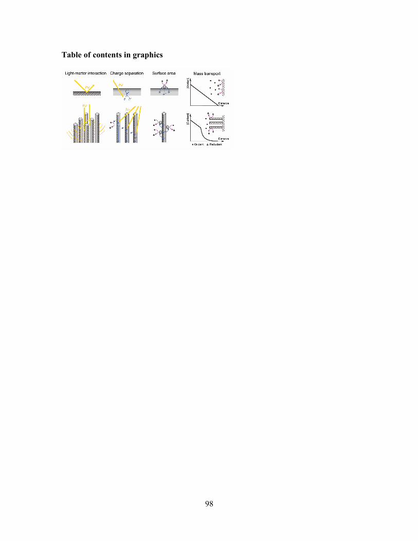
98
Table of contents in graphics