qt8p65c02n.pdf - eScholarship
78
UC San Diego UC San Diego Electronic Theses and Dissertations Title Towards a Modular, Low-Power, Low-Cost, and High-Speed Underwater Optical Wireless Communication Transmitter Permalink https://escholarship.org/uc/item/8p65c02n Author Gage, Christopher Paul Publication Date 2019 Supplemental Material https://escholarship.org/uc/item/8p65c02n#supplemental Peer reviewed|Thesis/dissertation eScholarship.org Powered by the California Digital Library University of California
-
Upload
khangminh22 -
Category
Documents
-
view
2 -
download
0
Transcript of qt8p65c02n.pdf - eScholarship

UC San DiegoUC San Diego Electronic Theses and Dissertations
TitleTowards a Modular, Low-Power, Low-Cost, and High-Speed Underwater Optical Wireless Communication Transmitter
Permalinkhttps://escholarship.org/uc/item/8p65c02n
AuthorGage, Christopher Paul
Publication Date2019
Supplemental Materialhttps://escholarship.org/uc/item/8p65c02n#supplemental Peer reviewed|Thesis/dissertation
eScholarship.org Powered by the California Digital LibraryUniversity of California

UNIVERSITY OF CALIFORNIA SAN DIEGO
Towards a Modular, Low-Power, Low-Cost, and High-Speed Underwater OpticalWireless Communication Transmitter
A thesis submitted in partial satisfaction of therequirements for the degree
Master of Science
in
Electrical Engineering (Applied Ocean Science)
by
Christopher Paul Gage
Committee in charge:
William Hodgkiss, Co-ChairJules Jaffe, Co-ChairGeorge Papen
2019

Copyright
Christopher Paul Gage, 2019
All rights reserved.
The thesis of Christopher Paul Gage is approved, and it is
acceptable in quality and form for publication on microfilm
and electronically:
Co-Chair
Co-Chair
University of California San Diego
2019
iii

DEDICATION
To my parents.
For teaching me to be constantly curious,
to always seek and treasure knowledge.
To my brother.
For teaching me that just because you cannot see or hear anything,
does not mean there is nothing to hear or see.
To my wife.
For always supporting me in following my dreams
and urging me to never settle for less.
iv

EPIGRAPH
We have a habit in writing articles published in scientific journals to
make the work as finished as possible, to cover all the tracks, to not
worry about the blind alleys or to describe how you had the wrong
idea first, and so on. So there isn’t any place to publish, in a
dignified manner, what you actually did in order to get to
do the work.
—Richard P. Feynman
v
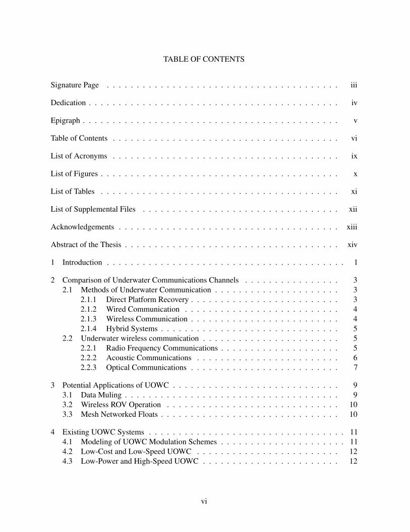
TABLE OF CONTENTS
Signature Page . . . . . . . . . . . . . . . . . . . . . . . . . . . . . . . . . . . . . . . iii
Dedication . . . . . . . . . . . . . . . . . . . . . . . . . . . . . . . . . . . . . . . . . . iv
Epigraph . . . . . . . . . . . . . . . . . . . . . . . . . . . . . . . . . . . . . . . . . . . v
Table of Contents . . . . . . . . . . . . . . . . . . . . . . . . . . . . . . . . . . . . . . vi
List of Acronyms . . . . . . . . . . . . . . . . . . . . . . . . . . . . . . . . . . . . . . ix
List of Figures . . . . . . . . . . . . . . . . . . . . . . . . . . . . . . . . . . . . . . . . x
List of Tables . . . . . . . . . . . . . . . . . . . . . . . . . . . . . . . . . . . . . . . . xi
List of Supplemental Files . . . . . . . . . . . . . . . . . . . . . . . . . . . . . . . . . xii
Acknowledgements . . . . . . . . . . . . . . . . . . . . . . . . . . . . . . . . . . . . . xiii
Abstract of the Thesis . . . . . . . . . . . . . . . . . . . . . . . . . . . . . . . . . . . . xiv
1 Introduction . . . . . . . . . . . . . . . . . . . . . . . . . . . . . . . . . . . . . . . . 1
2 Comparison of Underwater Communications Channels . . . . . . . . . . . . . . . . 32.1 Methods of Underwater Communication . . . . . . . . . . . . . . . . . . . . . 3
2.1.1 Direct Platform Recovery . . . . . . . . . . . . . . . . . . . . . . . . . 32.1.2 Wired Communication . . . . . . . . . . . . . . . . . . . . . . . . . . 42.1.3 Wireless Communication . . . . . . . . . . . . . . . . . . . . . . . . . 42.1.4 Hybrid Systems . . . . . . . . . . . . . . . . . . . . . . . . . . . . . . 5
2.2 Underwater wireless communication . . . . . . . . . . . . . . . . . . . . . . . 52.2.1 Radio Frequency Communications . . . . . . . . . . . . . . . . . . . . 52.2.2 Acoustic Communications . . . . . . . . . . . . . . . . . . . . . . . . 62.2.3 Optical Communications . . . . . . . . . . . . . . . . . . . . . . . . . 7
3 Potential Applications of UOWC . . . . . . . . . . . . . . . . . . . . . . . . . . . . 93.1 Data Muling . . . . . . . . . . . . . . . . . . . . . . . . . . . . . . . . . . . . 93.2 Wireless ROV Operation . . . . . . . . . . . . . . . . . . . . . . . . . . . . . 103.3 Mesh Networked Floats . . . . . . . . . . . . . . . . . . . . . . . . . . . . . . 10
4 Existing UOWC Systems . . . . . . . . . . . . . . . . . . . . . . . . . . . . . . . . . 114.1 Modeling of UOWC Modulation Schemes . . . . . . . . . . . . . . . . . . . . . 114.2 Low-Cost and Low-Speed UOWC . . . . . . . . . . . . . . . . . . . . . . . . 124.3 Low-Power and High-Speed UOWC . . . . . . . . . . . . . . . . . . . . . . . 12
vi

4.4 In Situ System Demonstrations . . . . . . . . . . . . . . . . . . . . . . . . . . 134.5 BlueComm Commercial System . . . . . . . . . . . . . . . . . . . . . . . . . 13
5 System Design . . . . . . . . . . . . . . . . . . . . . . . . . . . . . . . . . . . . . . 155.1 Current Enabling Technology . . . . . . . . . . . . . . . . . . . . . . . . . . . 15
5.1.1 Transmitting Hardware Technology . . . . . . . . . . . . . . . . . . . 155.1.2 Data Encoding Schemes . . . . . . . . . . . . . . . . . . . . . . . . . 16
5.2 Hardware Components . . . . . . . . . . . . . . . . . . . . . . . . . . . . . . 205.2.1 LEDs . . . . . . . . . . . . . . . . . . . . . . . . . . . . . . . . . . . . 215.2.2 LED Driver Circuit . . . . . . . . . . . . . . . . . . . . . . . . . . . . . 215.2.3 FPGA . . . . . . . . . . . . . . . . . . . . . . . . . . . . . . . . . . . 225.2.4 Custom PCBs . . . . . . . . . . . . . . . . . . . . . . . . . . . . . . . 225.2.5 Power-Measurement Resistor . . . . . . . . . . . . . . . . . . . . . . . 245.2.6 Power Supply . . . . . . . . . . . . . . . . . . . . . . . . . . . . . . . 27
5.3 Firmware Components . . . . . . . . . . . . . . . . . . . . . . . . . . . . . . 275.3.1 Test Pattern Project . . . . . . . . . . . . . . . . . . . . . . . . . . . . 275.3.2 Visual Media Demonstration Project . . . . . . . . . . . . . . . . . . . 295.3.3 Received Power Measurement Project . . . . . . . . . . . . . . . . . . 30
5.4 Modularity . . . . . . . . . . . . . . . . . . . . . . . . . . . . . . . . . . . . . 315.5 Power Consumption Measurement . . . . . . . . . . . . . . . . . . . . . . . . . 315.6 System Cost . . . . . . . . . . . . . . . . . . . . . . . . . . . . . . . . . . . . 33
6 System Tests . . . . . . . . . . . . . . . . . . . . . . . . . . . . . . . . . . . . . . . 346.1 Experimental Setup . . . . . . . . . . . . . . . . . . . . . . . . . . . . . . . . 34
6.1.1 Tank . . . . . . . . . . . . . . . . . . . . . . . . . . . . . . . . . . . . 356.1.2 Red Dye Addition . . . . . . . . . . . . . . . . . . . . . . . . . . . . 356.1.3 Photodetector . . . . . . . . . . . . . . . . . . . . . . . . . . . . . . . 366.1.4 Oscilloscope . . . . . . . . . . . . . . . . . . . . . . . . . . . . . . . 376.1.5 Data Test Pattern . . . . . . . . . . . . . . . . . . . . . . . . . . . . . 376.1.6 Visual Media Demonstration Test . . . . . . . . . . . . . . . . . . . . 39
6.2 Signal Processing . . . . . . . . . . . . . . . . . . . . . . . . . . . . . . . . . 406.2.1 Received Optical Power . . . . . . . . . . . . . . . . . . . . . . . . . 406.2.2 Power Measurement . . . . . . . . . . . . . . . . . . . . . . . . . . . 406.2.3 Data Test Pattern . . . . . . . . . . . . . . . . . . . . . . . . . . . . . . 416.2.4 Media Demonstration Test . . . . . . . . . . . . . . . . . . . . . . . . . 41
6.3 Results . . . . . . . . . . . . . . . . . . . . . . . . . . . . . . . . . . . . . . . . 416.3.1 Data Throughput Reduction . . . . . . . . . . . . . . . . . . . . . . . 426.3.2 Transmitter Rise Time . . . . . . . . . . . . . . . . . . . . . . . . . . 436.3.3 Power Consumption . . . . . . . . . . . . . . . . . . . . . . . . . . . 446.3.4 Test Pattern Bit Error Ratio . . . . . . . . . . . . . . . . . . . . . . . . 466.3.5 Image Series Test . . . . . . . . . . . . . . . . . . . . . . . . . . . . . 526.3.6 Video Demonstration Test . . . . . . . . . . . . . . . . . . . . . . . . 526.3.7 Summary . . . . . . . . . . . . . . . . . . . . . . . . . . . . . . . . . 58
vii

7 Evaluation of Thesis Success . . . . . . . . . . . . . . . . . . . . . . . . . . . . . . 59
8 Future Work . . . . . . . . . . . . . . . . . . . . . . . . . . . . . . . . . . . . . . . 608.1 Transmitter Hardware . . . . . . . . . . . . . . . . . . . . . . . . . . . . . . . 608.2 Shrinking and Customization of Receiver Hardware . . . . . . . . . . . . . . . . 61
Bibliography . . . . . . . . . . . . . . . . . . . . . . . . . . . . . . . . . . . . . . . . 62
viii

LIST OF ACRONYMS
AUV Autonomous underwater vehicle
BER Bit error ratio
BOM Bill of materials
COTS Commercial off-the-shelf
CTD Conductivity temperature and depth instrument
DPIM Digital pulse interval modulation
FPGA Field programmable gate array
GPIO General purpose input output
LED Light emitting diode
OOK On-off keying
PCB Printed circuit board
PLL Phase-locked loop
PPM Pulse position modulation
PWM Pulse width modulation
ROV Remotely operated vehicle
SPI Serial peripheral interface
UART Universal asynchronous receiver transmitter
UOWC Underwater optical wireless communication
WHOI Woods Hole Oceanographic Institute
ix

LIST OF FIGURES
Figure 2.1: The absorption spectrum of water . . . . . . . . . . . . . . . . . . . . . . 7
Figure 5.1: OOK encoding scheme example . . . . . . . . . . . . . . . . . . . . . . . 17Figure 5.2: 2-PWM encoding scheme example . . . . . . . . . . . . . . . . . . . . . 18Figure 5.3: 2-PPM encoding scheme example . . . . . . . . . . . . . . . . . . . . . . 19Figure 5.4: 2-DPIM encoding scheme example . . . . . . . . . . . . . . . . . . . . . 20Figure 5.5: LED Array16 PCB layout . . . . . . . . . . . . . . . . . . . . . . . . . . 23Figure 5.6: LED Array16 PCB schematic . . . . . . . . . . . . . . . . . . . . . . . . 24Figure 5.7: LED Driver PCB layout . . . . . . . . . . . . . . . . . . . . . . . . . . . 25Figure 5.8: LED Driver PCB schematic . . . . . . . . . . . . . . . . . . . . . . . . . 26Figure 5.9: A simple block diagram of the test pattern project . . . . . . . . . . . . . . 28Figure 5.10: A simple block diagram of the visual media demonstration project . . . . . 29Figure 5.11: Power measurement oscilloscope setup . . . . . . . . . . . . . . . . . . . 32
Figure 6.1: A system level view of the experimental setup . . . . . . . . . . . . . . . . 35Figure 6.2: The absorption spectrum for FD&C 40 red dye . . . . . . . . . . . . . . . 36Figure 6.3: Reduction in data throughput due to encoding scheme . . . . . . . . . . . 42Figure 6.4: Rise time of the optical transmitter . . . . . . . . . . . . . . . . . . . . . . 44Figure 6.5: Bits per Joule vs. data throughput . . . . . . . . . . . . . . . . . . . . . . 45Figure 6.6: Watts vs. data throughput . . . . . . . . . . . . . . . . . . . . . . . . . . 46Figure 6.7: Bit error ratio vs. incident power for on-off keying . . . . . . . . . . . . . 47Figure 6.8: Bit error ratio vs. incident power for pulse width modulation . . . . . . . . 48Figure 6.9: Bit error ratio vs. incident power for pulse position modulation . . . . . . . 49Figure 6.10: Bit error ratio vs. incident power for digital pulse interval modulation . . . 50Figure 6.11: Comparison of bit error ratio for different encodings at 5 Mbps . . . . . . . . 51Figure 6.12: The first transmitted test image, RS(255,223) coded. . . . . . . . . . . . . 53Figure 6.13: The first transmitted test image, with no error correction . . . . . . . . . . 53Figure 6.14: The second transmitted test image, RS(255,223) coded. . . . . . . . . . . . 54Figure 6.15: The second transmitted test image, with no error correction . . . . . . . . . 54Figure 6.16: The third transmitted test image, RS(255,223) coded. . . . . . . . . . . . . 55Figure 6.17: The third transmitted test image, with no error correction . . . . . . . . . . 55Figure 6.18: The fourth transmitted test image, RS(255,223) coded. . . . . . . . . . . . 56Figure 6.19: The fourth transmitted test image, with no error correction . . . . . . . . . 56Figure 6.20: The fifth transmitted test image, RS(255,223) coded. . . . . . . . . . . . . 57Figure 6.21: The fifth transmitted test image, with no error correction . . . . . . . . . . 57
x

LIST OF TABLES
Table 5.1: The bill of materials for the 16 LED transmitter . . . . . . . . . . . . . . . 33
Table 6.1: The oscilloscope settings for each project . . . . . . . . . . . . . . . . . . . 38
xi

LIST OF SUPPLEMENTAL FILES
Supplemental File 1: . . . . . . . . . . . . . . . . . . . . . . . . . . . gage binary sofs.zipSupplemental File 2: . . . . . . . . . . . . . . . . . . . . . gage RS encoded video 0.movSupplemental File 3: . . . . . . . . . . . . . . . . . . . . . gage RS encoded video 1.movSupplemental File 4: . . . . . . . . . . . . . . . . . . . . . gage RS encoded video 2.movSupplemental File 5: . . . . . . . . . . . . . . . . . . . . . . . . . . . gage schematics.zipSupplemental File 6: . . . . . . . . . . . . . . . . . . . . . . . . gage source encoders.zipSupplemental File 7: . . . . . . . . . . . . . . . . . . . . gage source media download.zipSupplemental File 8: . . . . . . . . . . . . . . . . . . . . . . . gage source processing.zipSupplemental File 9: . . . . . . . . . . . . . . . . . . . . . gage source received power.zipSupplemental File 10: . . . . . . . . . . . . . . . . . . . . . . . gage source transmitter.zip
xii

ACKNOWLEDGEMENTS
Thank you to my advisor, Jules Jaffe, for your time, experience, and vision. Thank you
as well to my other committee members, William Hodgkiss and George Papen, for taking the
time to review and evaluate my thesis. Thank you to Paul Roberts for helping with the nitty-gritty
details and for always having suggestions on how to solve technical issues. I would also like to
thank the UCSD ECE department for helping to fund my work on this thesis.
Thank you to my AOS cohort, Billy, Bofu, Eric, Kelley, Michelle, and Narda, for enduring
lots of math and MATLAB with me.
Finally, thank you to Michelle DeRienzo, for her unwavering belief in my capabilities, for
all of her revisions, and for dealing with me waking in the middle of the night to write.
xiii

ABSTRACT OF THE THESIS
Towards a Modular, Low-Power, Low-Cost, and High-Speed Underwater OpticalWireless Communication Transmitter
by
Christopher Paul Gage
Master of Science in Electrical Engineering (Applied Ocean Science)
University of California San Diego, 2019
William Hodgkiss, Co-ChairJules Jaffe, Co-Chair
This thesis demonstrates an underwater optical wireless communication transmitter. The
transmitter has been designed to make it easy to add on to any system, while having a minimal
impact on project power and cost budgets. The hardware designed for this thesis is capable of
transmitting at speeds up to 8.88 Mbps with bit error ratios on the order of 10−5 to 10−2 at a
received optical power from -19.2 to -27.5 dBm. The transmitter consumes 1.75 W of power and
has a bill of materials cost of $41.95. This thesis demonstrates the transmission of a 720p, one
frame-per-second video with a simple RS(255,223) encoding.
xiv

1 Introduction
Underwater optical wireless communication (UOWC) is a relatively young field that has
gained considerable interest over the past decade. This increase in interest has been largely due
to the availability of commercial off-the-shelf (COTS) electronics components that decrease
the system complexity, cost, and power consumption. UOWC is targeted as a short-range
replacement for the current dominant underwater wireless communication technology, acoustic
wave communication. UOWC is appealing as it solves the issues of low bandwidth, long latencies,
and high power consumption that are associated with acoustic communication. Addressing these
issues allows the use of wireless communication in a variety of new situations.
Thesis Statement: This thesis describes the design of a UOWC transmitter optimized for
modularity, cost, power consumption, and speed. The aim is to create and evaluate a system with
a low enough cost and power consumption to allow for the inclusion of UOWC in projects of
any size. The design should also be simple enough that the system is easy to expand or adapt to
a specific project’s needs. The design uses modern COTS components along with two simple
custom printed circuit boards (PCBs) to keep costs low and allow modularity. The design uses
light emitting diodes (LEDs) as the optical generator to limit the power consumption. The design
uses a field programmable gate array (FPGA) to encode and transmit data which allows for
precise control of the bitstream. The major contributions of this thesis are:
• The design of a modular, low-cost, low-power, and high-speed underwater optical wireless
transmitter using COTS electronic components.
1

• The implementation of four common UOWC bitstream encodings on an FPGA.
• A comparison of the power consumption of each of the bitstream encodings.
• A comparison of the bit error ratio (BER) of each of the bitstream encodings with varying
received light power.
• Proof-of-concept transmissions of an image sequence and a video.
This thesis is organized as follows: Chapter 2 describes the trade-offs between various
methods of underwater communication. Chapter 3 describes applications that would benefit from
low-cost, low-power, and high-speed UOWC. Chapter 4 describes previous work on modular, low-
cost, low-power, and high-speed UOWC systems and shows two example applications of UOWC.
Chapter 5 describes the design of the transmitter system constructed for this thesis. Chapter 6
describes the tank experiment setup and signal processing, then discusses the performance test
and proof-of-concept image and video transmission results. Chapter 7 discusses how well the
goals of the thesis were met. The thesis concludes in Chapter 8 with a discussion about potential
future improvements on the design of the transmitter and the creation of a full UOWC modem.
2
2 Comparison of Underwater
Communications Channels
Communication underwater is difficult, largely due to the physical properties of the
medium. This chapter will discuss the main methods of underwater communication and several
different wireless underwater communication channels.
2.1 Methods of Underwater Communication
There are several broadly defined methods for retrieving scientific data from underwater
platforms.
2.1.1 Direct Platform Recovery
The first and simplest method for retrieving data is direct platform recovery. This can take
several forms, one of which is a conductivity temperature and depth instrument (CTD) cast where
the instrument is deployed off of a vessel or pier and then reeled back in. Another example is
dropping long term fish tag loggers connected to weights. These are left in place for the study
period and then mechanically disconnected from the anchoring weight by an acoustic trigger and
retrieved once they float to the surface. In both of these cases, the data is retrieved only after the
physical platform is recovered.
3

An example of a CTD is the SBE 25plus Sealogger CTD which requires the data to be
downloaded after a profile is taken [1]. This can mean that interesting features of the profiled
water column are difficult to react to dynamically.
Similarly, in the case of the fish tag logger, there is a large data latency, which can again
impede researcher’s abilities to quickly follow up on interesting patterns. This method requires at
least two trips to the site to collect data for one study, one to place the logger and one to retrieve
it. It is also possible that the trigger may not activate, causing all of the data to be lost.
2.1.2 Wired Communication
The next method of communication is a direct cable attachment to the instrument platform.
The most familiar example of this type of communication is a remotely operated vehicle (ROV),
where the cable provides power to the vehicle and gives the operator real-time video feedback,
allowing direct control.
A direct cable connection allows the user to control the platform directly and collect data
in real-time. A major benefit to using a cabled connection is that power can be simultaneously
delivered via the same cable, allowing the project to have a much larger power budget.
Downsides of using this method are that it is costly, it is difficult to maintain and deploy
large lengths of cable, and the reachable area is limited to the length of the cable available. The
cable can also be tangled or broken by a careless operator or in rough seas.
2.1.3 Wireless Communication
Another method for retrieving data is wireless communication. An example of wireless
communication is using multiple autonomous underwater vehicles (AUVs) to track a tagged
shark [2]. Here, the wireless communication was accomplished using an acoustic modem, which
severely limited the rate at which the AUVs were able to exchange information.
4

Wireless communication has some attractive features including real-time feedback and
the removal of expensive cabling. However, current wireless technologies are typically rela-
tively low-speed, power-hungry, and expensive. Range can also be a concern depending on the
communication technology being used.
2.1.4 Hybrid Systems
Hybrid systems can also be created with a combination of the methods listed above. An
example of this would be an ocean mooring where there are sensors deployed along the anchoring
cable that report to a top-side controller via a cable. From there, a wireless cellular connection
can transmit the data to the shore in real-time. This can help play to the strengths of each method,
but makes for a more complex system that is more difficult to integrate and maintain.
2.2 Underwater wireless communication
There are several different communication technologies that can be used for underwater
wireless communications, each with its advantages and disadvantages. This section considers
three of these technologies and their suitability for use underwater wireless communications.
2.2.1 Radio Frequency Communications
Radio frequency communication is the mainstay of the modern world, used in cellular,
satellite, and WiFi communication technology. Radio frequency communications rely on the
modulation (typically frequency or amplitude) of electro-magnetic waves of wavelength 10
meters to 10 kilometers. One example of a platform that uses radio frequency communication
is OceanServer’s IVER2 AUV [3]. It uses WiFi when surfaced to receive commands and to
quickly download data without a direct cable connection. Since there is significant knowledge
in this area to draw on, it is an enticing avenue for adaptation. Unfortunately, seawater is nearly
5

opaque to radio frequencies due to its conductivity [4], rendering it useful only for very short
range communication, surface operations, or hybrid systems.
2.2.2 Acoustic Communications
The most mature underwater wireless communication method is acoustic communication.
Acoustic communication is often done with phase-shift keying of the acoustic signals. One
application of acoustic communication is to use it to coordinate between multiple AUVs to track a
tagged shark [2]. In this application, the acoustic modem allows the AUVs to share their tracking
information in real-time.
Acoustic communication has some very appealing features. The first is that it has a long
range, several km [5] in the frequency bands that are used most often. Another benefit is that the
technology for acoustic communication is quite mature, with numerous ready to integrate options
on the market, including the Woods Hole Oceanographic Institute (WHOI) µModem [6].
One drawback of acoustic modems is that the cost for a WHOI µModem is around $8000-
$9000. Due to the high cost, it is only practical for a small number of large stations. Another
downside of the acoustic communication channel is that the range is inversely proportional to the
frequency of the sound, which is in turn directly proportional to the bandwidth. This means that
a trade off has to be calculated between range and bandwidth. Acoustic modems are therefore
typically limited to a bandwidth on the order of several Kbps [6] to achieve their kilometers-long
range. This precludes any hope of real-time direct control with visual feedback as there is not
enough bandwidth to return high-quality video. Another limitation is the high latency due to
the speed of sound in water (∼1500 meters/second), meaning that communication from just two
kilometers away through water has similar latency to communication between Earth and the
Moon. Finally, in part due to the low bitrate, acoustic modems use a lot of energy for each data bit
they transmit, as measured by bits per Joule. Acoustic modems have a typical efficiency of ∼100
bits/Joule [5]. This is crucial because a wireless platform must rely entirely on battery power, so
6

any additional power requirement increases the cost and weight of the entire platform.
2.2.3 Optical Communications
A relatively new channel that is being explored is the optical channel. This channel uses
electro-magnetic radiation in the visible spectrum, with wavelengths from 400 nm to 700 nm. The
absorption of electro-magnetic radiation in water has a minimum around 200 nm wavelengths, as
shown in Figure 2.1. Because of this minimum, using shorter wavelength light is a viable method
of wireless communication. This dip in absorption coefficient allows the leverage of an extensive
number of COTS electronic components that generate visible light, especially in the blue-green
wavelengths.
Figure 2.1: The absorption spectrum of water. Note the deep dip near the blue-green visiblelight wavelengths. [7]
An advantage of the optical channel is that it allows high speed data transfer on the order
of Mbps[8] to Gbps[9]. Optical communications also have a low latency due to the speed of light
in water. Given the wealth of simple COTS components that emit and detect light, discussed
7

in detail in Section 5.1.1, the design and construction of these systems is relatively simple and
inexpensive. Compared with the acoustic channel on a per bit basis, optical communication is
much more energy efficient with a previously demonstrated efficiency of ∼30,000 bits per Joule
[5]. This thesis demonstrates further improvement on energy efficient optical communication.
The main drawback of optical communication is that the range is limited to 1-100 meters
[5]. This range is highly dependent on the water conditions, as light will not only be attenuated
by the water, but also scattered by particulate matter suspended in the water [4]. Another
drawback is that optical communication typically require a direct line-of-sight between receiver
and transmitter.
8

3 Potential Applications of UOWC
This thesis targets UOWC for specific situations where a wireless, low-cost, low-power,
and/or high-speed communication link is required. Three such applications are detailed in this
chapter.
3.1 Data Muling
One useful application of UOWC is to retrieve data from permanent ocean floor instal-
lations. This would involve an AUV approaching and interrogating the permanent platform via
UOWC, allowing the platform to quickly transmit its data to the AUV. Using a simple AUV
would also reduce the cost of accessing the platform by allowing both cruises of opportunity and
smaller and less capable vessels to be used. This would allow more frequent data downloads
and thereby decrease the latency of data. A team at WHOI has successfully demonstrated this
capability by retrieving data from a seafloor borehole observatory [5].
A low-power UOWC solution enables this application by allowing the ocean floor instal-
lation to run on battery and not use all of its battery for data transmission. A high-speed UOWC
would allow large amounts of data to be transmitted relatively quickly, which would save on boat
time as well as power consumption.
9

3.2 Wireless ROV Operation
Another interesting application is to use UOWC to wirelessly operate an ROV. This
requires two-way high speed communication to facilitate sending commands to and receiving
video from the vehicle. The communication also needs to be power efficient as the wireless ROV
would run solely on battery power. The WHOI team has also demonstrated this capability over a
range of 15 meters [5].
A low-power UOWC solution enables this application possible by allowing the ROV
to run on battery and not use all of its battery for image transmission and control signals. A
high-speed UOWC would allow real-time control to be achieved, with images returned to the
operator to guide them.
3.3 Mesh Networked Floats
A third application of UOWC is to take a group of small floats [10] and create a UOWC
mesh network. In this case, multiple users would need to be accommodated by a network
multiplexing of the signal instead of using different wavelengths of light. One potential method
would be time division multiple-access, which allots each device on the network a certain slice of
time to transmit its data. This would be necessary because with so many transceivers, it would
not be practical for each of them to have a different carrier wavelength. This application could
also be utilized to improve the range of the UOWC by relaying information from float to float
through the mesh network.
For this application, a low-cost solution would be essential. This is because the number
of floats, each needing their own modem, is much larger than in the AUV or ROV applications
outline in the previous sections. The solution would also need to be power efficient to keep the
battery weight down because buoyancy must be maintained in these small floats.
10

4 Existing UOWC Systems
There are a fair number of groups researching UOWC, and the results they have demon-
strated are quite impressive, with a maximum reported performance of 4.8 Gbps over 5.4 meters
[9]. However, there has not been much work done to improve the power and cost efficiency
of UOWC systems. There are two teams that have recently published systems that aim to fit
in this niche, and some interesting modeling work has also been done. Two other groups have
demonstrated some in situ applications of UOWC, one from WHOI and another from the MIT
Computer Science and Artificial Intelligence Lab (CSAIL). An example of a commercial UOWC
system is also discussed in this chapter.
4.1 Modeling of UOWC Modulation Schemes
This thesis investigates four different data encoding schemes as described in Section 5.1.2.
A group at Institut Fresnel in France has performed some modeling of the same encoding schemes
[11]. The Institut Fresnel group’s modeled system is very similar to the one realized in this thesis,
so a description and some comparisons to the model should be instructive. The modeled system
assumed a transmitted power of 20 dBm, a 532 nm LED with an emission angle of 20 degrees,
and a transmission rate of 100 Mbps. The receiver was modeled as a PIN photodiode as the
detector with a 20 cm collimating lens.
Their model showed that the best BER was obtained using pulse position modulation
11

(PPM), next best with on-off keying (OOK) and digital pulse interval modulation (DPIM), and
the worst encoding was pulse width modulation (PWM). One interesting feature of the model is
that the BER of the DPIM encoding quickly plateaued, going from below 10−7 to over 0.1 in a
few meters.
4.2 Low-Cost and Low-Speed UOWC
There is a group at the University of Lisbon that has performed a study of different
modulation schemes in their “Blue Ray” optical modem [12]. This modem has a transmitter cost
of around $100, a transmitter power consumption of 24 W (mostly from the LEDs), a range of 5
meters, and a maximum data rate of 200 Kbps. It also uses green LEDs that have lenses to reduce
the emission angle to 12 degrees, and has a PIN photodiode as the receiver. While the system has
a very reasonable cost, it has an efficiency of only 8333 bits per Joule, and is fairly slow at 200
Kbps, which is far too slow for real-time image or video transmission. The cost, efficiency, and
speed are all improved upon in this thesis.
4.3 Low-Power and High-Speed UOWC
A group at the University of Science and Technology of China has demonstrated an
FPGA based, 25 Mbps UOWC system that has a range of 10 meters [13]. This system has a
transmitter cost of around $150, and uses 1 W of power. It transmits an OOK encoded signal
using a high-speed digital to analog converter and a 448 nm LED with a collimating mirror that
reduces the emission angle to 2.5 degrees. The receiver uses an avalanche photodiode and a
10 cm diameter convergent lens. Some of the disadvantages of this system are that high-speed
digital-to-analog converters and avalanche photodiodes are expensive and complex to use. Also,
the small emission angle means that the system needs to be carefully aligned. While $150 is fairly
12

inexpensive, this thesis demonstrates a system with lower cost..
4.4 In Situ System Demonstrations
The WHOI group demonstrated error free 1 Mbps communication at a range of 100
meters in deep water [5]. This range was achieved in a highly optimized environment. Testing
was completed at a depth of 2400 meters, where there is little optical noise due to light filtering in
from the sea surface and the water is much clearer than in the littoral zone. WHOI has also done
research into diffuse (non-directional) optical wireless communication with vertical ranges of up
to 200 meter at 5 Mbps in the clearest water [8]. WHOI has also created two-way communication
links using one transmitter with a blue LED and another with a green LED to decrease self
interference from scattering [5].
A group at MIT CSAIL has developed a system called AquaOptical [14]. There are two
variants, a high power system and low power system. The high power system uses six 5W LEDs
for transmission and an avalanche photodiode for detection. The low power system uses one 5W
LED for transmission and an inexpensive PIN photodiode for detection. The group has performed
testing at shallow depths in Singapore Harbor, with high powered ranges of up to 8 meters at
data rates of 333 Kbps in very turbid waters [14]. The group has also attached their AquaOptical
technology to a vehicle called the Autonomous Modular Optical Underwater Robot (AMOUR).
This vehicle has also been tested in shallow water in Singapore Harbor. Control of the AMOUR
vehicle was achieved at a range of 7 meters using a 600 Kbps bitrate[15].
4.5 BlueComm Commercial System
Sonardyne has a commercial UOWC system called BlueComm [16]. This system has a
range of up to 150 meters at a 10 Mbps data rate and a maximum data rate of 500 Mbps over 7
13

meters. However, to obtain that 150 meter range, there must be little to no ambient light, and a
photomultiplier tube is used for receiving data, which is a very delicate and expensive instrument.
The system can transmit approximately 105 bits per Joule, which is more efficient than most of
the other systems reviewed in this chapter. This efficiency is improved upon in this thesis.
14

5 System Design
This thesis is focused on creating an underwater optical wireless transmitter, with the
goal of making the transmitter modular, low-power, low-cost, and high speed. The hardware was
designed to meet these goals by selecting components to minimize power and cost. High-speed
for this thesis means a maximum of 10 Mbps, enough to transmit high quality video and images.
In terms of modularity, the system is designed to be easy to “bolt on” to any existing system. It is
also possible to switch out components if an application requires a modified solution.
5.1 Current Enabling Technology
Over the past decade, research into UOWC has begun to accelerate, in large part due to
the availability of relatively low cost, high speed, COTS electrical components. This section
contains a summary of the current enabling technology.
5.1.1 Transmitting Hardware Technology
There are two main types of optical components that are used for transmitting optical
signals underwater. They are LEDs and laser diodes.
LEDs have the advantage of being cheap, easy to integrate, relatively robust, and power
efficient. They also have a relatively wide emission angle of up to 120 degrees [17]. A wide
emission angle is an advantage because it eases the alignment requirements on the platform. This
15

reduces the configuration complexity and reduces the danger of losing the transmission link due to
slight receiver or transmitter motion. The downside is that only a fraction of the power is observed
by the receiver, thus reducing the range that is possible from a given number of generated photons.
This issue could be mitigated by using an array of receivers or using a lens to focus light from a
wider area onto a smaller receiver.
Laser diodes are similar to LEDs, however they have a higher intensity and more directed
emission of light. Since they are more directional, they impose tighter alignment requirements on
the platform, but their directionality and higher power allow for longer communication distances.
They can also have faster switching times, enabling higher bitrates [4]. Laser diodes are also
more complex to drive electronically, and consequently more expensive to operate.
Designing the encoding logic and processing has become easier with cheaper, more
efficient, and smaller form-factor COTS FPGA development boards. Using an FPGA instead of a
microcontroller allows for more flexibility and precision in encoding schemes, as well as reducing
the amount of time it takes to implement a given scheme. FPGAs also offer the capability to
easily change the interface that data is sourced from, allowing options such as shared RAM, a
simple universal asynchronous receiver transmitter (UART) bus, or a serial peripheral interface
(SPI) bus.
5.1.2 Data Encoding Schemes
There are numerous ways to encode data for transmission over an optical link. Some use
multiple independently controlled laser diodes [9], which are used to increase the throughput
of the system. The downside to these methods is that they greatly increase the complexity of
encoding and decoding hardware and software.
This thesis investigates single-stream data encoding schemes transmitted by multiple
LEDs. Using single-stream encoding schemes reduces the complexity of detection; having many
LEDs boosts the signal intensity so that LEDs can be used to relax the alignment requirements.
16

Four common single-stream data encoding schemes were investigated for this thesis to
determine the effect they have on data throughput, bit error ratio, and power consumption. The
Verilog implementation of each of these encoding schemes can be found in Supplemental File 6.
The data was placed into a simple packet of 4096 bytes with a start and stop byte. The
start/stop bytes were chosen specifically for each encoding so that the first bit of the encoding
was a one and there were several level transitions. This gave a definite start and stop to the packet
and enough change in the level to make the matched filtering easier. Each byte was transmitted
least significant bit first and had a single zero as a stop bit.
On-Off Keying
OOK is the typical serial bit encoding scheme, where a single clock cycle of an off LED
represents a logical zero, and a single cycle of an on LED represents a logical one. See Figure 5.1
for an example of the OOK encoding used in this thesis.
Figure 5.1: OOK encoding scheme example. This example shows how the byte 0xE4(b11100100) would be encoded. The tick marks delineate single transmitted bits.
OOK is the fastest encoding scheme because there is a one to one correspondence between
the data bits and transmitted bits. The actual throughput will be slightly less than the transmitted
bit rate due to the addition of a stop bit and the start/stop bytes.
The implementation of the OOK encoder can be found in the encoderOOK.v file.
The start/stop byte used for OOK was b01010101. This byte was chosen because it
provides enough edges to be easy to capture and distinguish from random noise and because the
first bit transmitted will be a one as it is transmitted least significant bit first.
17

Pulse Width Modulation
PWM is an encoding that is generated by taking n bits of the data to be transmitted and
encoding them in 2n transmitted bits. In PWM, these 2n bits are used to send a pulse beginning at
a high level for the first bit. The subsequent width of the pulse is determined by the value that is
being transmitted.
Figure 5.2: 2-PWM encoding scheme example. This example shows how the byte 0xE4(b11100100) would be encoded. The tick marks delineate single transmitted bit periods, and thehashed marks delineate two data bits.
For this thesis, a value of n = 2 was used, which is referred to as 2-PWM. With n = 2,
every two bits of a byte were encoded and transmitted as four bits over the optical link. See
Figure 5.2 for an example of the 2-PWM encoding used in this thesis. As 2-PWM requires four
transmitted bits to encode two data bits, this encoding scheme reduces the data throughput of the
system by a factor of two. The stop bit and start/stop bytes also decrease the throughput slightly.
The implementation of the 2-PWM encoder can be found in the encoder2PWM.v file.
The start/stop byte used for PWM was b11100100. For PWM, the first bit in every
encoded byte will always be a one so forcing the first bit on was not a factor in the decision of the
start/stop byte value. This value was chosen because it demonstrates that each 2-bit pattern can
be detected and it has enough transitions to easily distinguish the byte from random noise.
Pulse Position Modulation
PPM is an encoding that is generated by taking n bits of the data to be transmitted and
encoding them in 2n transmitted bits. In PPM, these 2n bits are used to send a single transmitted
18

bit width pulse whose position is determined by the value that is being transmitted. So in PPM
encoding, the position of a single pulse is modulated, whereas in PWM, the width of a single
pulse is modulated.
Figure 5.3: 2-PPM encoding scheme example. This example shows how the byte 0xE4(b11100100) would be encoded. The tick marks delineate single transmitted bit periods, and thehashed marks delineate two data bits.
For this thesis, a value of n = 2 was used, which is referred to as 2-PPM. With n = 2,
every two bits of a byte were encoded and transmitted as four bits over the optical link. See
Figure 5.3 for an example of the 2-PPM encoding used in this thesis. As 2-PPM requires four
transmitted bits to encode two data bits, this encoding scheme reduces the data throughput of the
system by a factor of two. The stop bit and start/stop bytes also decrease the throughput slightly.
The implementation of the 2-PPM encoder can be found in the encoder2PPM.v file.
The start/stop byte used for PPM was b11100100. For PPM, the first two data bits must be
b00 to ensure that there were no leading zeros before the first on pulse. This value was also chosen
because it demonstrates that each 2-bit pattern can be detected and it has enough transitions to
easily distinguish the byte from random noise.
Digital Pulse Interval Modulation
DPIM is an encoding that is generated by taking n bits of data and encoding them in a
variable length of 2 to 2n +1 transmitted bits. These transmitted bits are structured as a single
transmitted bit time on pulse, followed by 1 to 2n off pulses, with the number of off pulses
determined by the value of the two data bits being encoded.
19

Figure 5.4: 2-DPIM encoding scheme example. This example shows how the byte 0xE4(b11100100) would be encoded. The tick marks delineate single transmitted bit periods, and thehashed marks delineate two data bits.
For this thesis, a value of n = 2 was used, which is referred to as 2-DPIM. With n = 2,
every two bits of a byte are encoded as two to five bits over the optical link. See Figure 5.4 for an
example of the 2-DPIM encoding used in this thesis. Assuming an even distribution of two bit
values, 2-DPIM requires an average of 3.5 transmitted bits to encode two data bits. This leads to
a throughput of 0.57 times the data clock rate, slightly better than 2-PWM and 2-PPM. The stop
bit and start/stop bytes will also decrease the throughput slightly.
The implementation of the 2-DPIM encoder can be found in the encoder2DPIM.v file.
The start/stop byte for DPIM is b00000000. For DPIM, the first bit in every encoded byte
will always be a one so forcing the first bit on was not a factor in the decision of the start/stop
byte value. This value was chosen because it is the shortest pattern and so has the least effect on
throughput.
5.2 Hardware Components
The scope of this thesis includes designing, prototyping, testing, laying out, and assem-
bling the electronic hardware for the UOWC transmitter. This section contains a description of
the finalized transmitter hardware. The transmitter uses three different boards which are layered
on top of each other. The total size of the transmitter is 4 cm thick, 4.8 cm wide, and 6.3 cm long.
The first board holds the transmitting LEDs, with 16 LEDs arranged in a four by four array. The
next board is the LED driver board, which converts the digitally encoded signal into an analog
20

signal to drive the LEDs. The final board is an FPGA development board, which encodes the data
and generates the digital bitstream. The Eagle CAD files can be found in Supplemental File 5.
5.2.1 LEDs
The LEDs used for this thesis were 5 mm round LEDs that emit at 470 nm with an
emission angle of 15 degrees [18]. These LEDs were chosen to take advantage of the decrease
in the absorption of light in water in the blue wavelengths. An array of 16 of these LEDs was
used to produce enough light to successfully transmit through the water. A large number of
lower-intensity LEDs were used instead of a small number of high intensity LEDs due to concerns
about the rise time of the higher power LEDs and their very wide emission angles.
5.2.2 LED Driver Circuit
In order to transmit the digital signal encoded by the FPGA, a driver was required that
could switch the LEDs on and off without drawing too much current from the FPGA. With this
goal in mind, the LED driver described by Gioux [19] was chosen. This driver was chosen for
the low component cost, the simplicity of the design, and because the bandwidth of 35 MHz was
large enough to accommodate the target maximum LED switching frequency of 10 MHz.
The implementation of Gioux’s LED driver in this thesis, shown in Figure 5.8, is largely
unchanged from that described in [19]. The main difference is that the MOSFET was upgraded
to a device that has a higher current rating [20], 2.5 A instead of 150 mA. This change allowed
more LEDs to be used. There are also some slightly different resistor values in the operational
amplifier feedback loop, due to the resistor values that were readily available in the lab.
21

5.2.3 FPGA
The digital encoding of data was performed on an FPGA, which was chosen for its
flexibility and the ease of implementing the different target encodings. A development board
was used to help reduce the design complexities associated with FPGAs, such as difficult power
supplies, the interface with the development computer, and chip packages that are difficult to
hand solder.
Originally, the PIF 2 FPGA development board was investigated for use as the digital
encoder. This was of interest due to its close integration with the Raspberry Pi. The FPGA used
on this development board is a Lattice MachXO3 FPGA. However, it was found that debugging
the Verilog on the board was very difficult, especially with bugs that did not show up in simulation.
For this reason, an alternative FPGA development board was selected.
The new FPGA development board selected was the Arrow MAX1000 board which has
an Altera MAX10 FPGA on it, as well as some useful external RAM and Flash memory. One
reason for picking this device was the NIOSII soft processor that is available on the MAX10. This
feature allows for control of the transmission to be easily moved from an external Raspberry Pi to
an on-board soft processor, decreasing the cost, power, and complexity of the system. Another
advantage is the on-board JTAG blaster. This feature allows the Verilog signal waveforms to
be directly recorded on the development computer, making debugging much simpler. The final
advantage was the author’s familiarity with the MAX10 FPGA and its integrated development
environments.
5.2.4 Custom PCBs
Two custom PCBs were designed and laid out for this thesis. The two boards are the LED
array board and a 16-LED driver board. These PCBs were manufactured by JLCPCB and the
schematics and board layouts can be found in Figures 5.5-5.8.
22

16-LED Array Board
The 16-LED board layout is shown in Figure 5.5 and the array schematic is shown
in Figure 5.6. The LEDs on this board are arranged in a four by four array for ease of layout.
Breaking the LEDs out onto a separate board allows the end user to create the LED array geometry
that best suits their application. This board is 48 mm by 48 mm, which is allows space for a loose
packing of the 16 LEDs plus the connector hardware.
Figure 5.5: LED Array16 PCB layout. The top(red) and bottom(blue) planes are connected toground.
LED Driver Board
The LED driver board layout is shown in Figure 5.7 and the schematic is shown in Figure
5.8. This board is 63 mm by 48 mm, but could be laid out in a much smaller footprint, especially
23

Figure 5.6: LED Array16 PCB schematic.
if surface mount components were used instead of through-hole components. Another potential
size optimization is that the power resistor, R1 in Figure 5.8, and test points could be omitted
since they are present only for characterization. This size board was chosen to make the board
length the same as the length of the MAX1000 development board and to make the width the
same as that used for the 16-LED array board.
5.2.5 Power-Measurement Resistor
In order to measure the power consumption of the transmitter, a current sense resistor
(R1) was used. This resistor has a value of 0.02±1%Ω, and is placed in series with the power
supply and the rest of the circuit.
To find the power, the voltage drop over the sense resistor was measured and divided by
the resistance to calculate the current supplied to the board. After applying Ohm’s law, the current
was multiplied by the voltage drop of the circuit, giving the instantaneous power draw of the
circuit. The instantaneous power draw was then integrated over the transmission time to calculate
the total energy used during a transmission.
24

Figure 5.7: LED Driver PCB layout. The top(red) and bottom(blue) planes are connected toground. R1 is the power sense resistor. Most traces are on the top plane, except for those comingfrom G12, which can be seen branching left and right from the G12 pin on JP1, the FPGAconnector.
25

Figure 5.8: LED Driver PCB schematic.
26

5.2.6 Power Supply
The power supply used was a Lambda Model LGD-422 Dual Regulated Power Supply. It
was set to power the system at 5V.
5.3 Firmware Components
The firmware for this thesis was mainly written in Verilog, with some controlling code
written in C, and can be found in a git repository hosted at https://bitbucket.org/scrippsuowc/
uowcsio public/. The encoding of data was performed by the MAX10 FPGA, independent of
the particular code project and can be found in Supplemental File 6. There were three separate
projects, the first transmitted a test pattern stored in ROM, the second transmitted demonstration
images and a video stored in the on-board SPI flash, and the last was used to determine the optical
power measured by the receiver under different communication channel conditions. Each project
generates a binary .SOF file to be downloaded to the FPGA. The generated binaries used for
testing can be found in Supplemental File 1.
5.3.1 Test Pattern Project
The test pattern project is a combination of Verilog and C code. The Verilog portion
instantiates the encoders, a state machine controlling the packetization and transmission of data,
and a soft-core NIOSII processor. The C code then runs on the NIOSII processor and commands
the state machine to send a packet of data. The flow of control can be seen in the block diagram
in Figure 5.9. The source code for this project is located in Supplemental File 10.
Verilog Code
The Verilog code for the test pattern project instantiates a number of modules that are
necessary to control the encoding of data bytes and the transmission of that encoded data. The
27

Figure 5.9: A simple block diagram of the test pattern project.
top.v module uses a phase-locked loop (PLL) that takes the on-board 12 MHz crystal oscillator
and generates a 100 MHz clock for processor operations and a 10 MHz clock for transmission
operations. This module also takes control signals from the NIOSII processor that determine what
data rate and encoding to use for a given transmission, as well as when to start that transmission.
The module sends back a tx ready signal once the previous transmit command has been completed
and another can be performed.
Once a transmission has been initiated by the NIOSII processor, the main state machine
in the top.v module takes control of the proper packetization and transmission of the data. The
state machine first sends the start byte to the encoder, and then iterates through each of the 4096
bytes stored in the test pattern ROM and sends them to the encoder. Once the state machine has
iterated through all of the data, it sends the stop byte to the encoder and returns to an idle state,
signaling to the NIOSII processor that the transmission has been completed.
28

C Code
The controlling C code is found in main.c. This code iterates through each combination
of encoding and clock rate of interest. For this experiment, a breakpoint was placed between each
different encoding so that the encodings could be easily broken up into different record files.
The shared code modem tx.c and modem tx.h deals with properly setting the general
purpose input output (GPIO) signals that control the encoding selection, data rate selection, and
transmission triggering.
5.3.2 Visual Media Demonstration Project
The visual media demonstration project is constructed largely along the same lines as
the test pattern project discussed in Section 5.3.1. The main differences are the source of the
transmitted data and how the controlling code in the NIOSII processor instructs the Verilog code
on the FPGA to access the data. The code for this project can also be found in Supplemental File
10. The flow of control can be seen in the block diagram in Figure 5.10.
Figure 5.10: A simple block diagram of the visual media demonstration project.
29
Data Storage
The demonstration images and video are stored on the MAX1000’s on-board SPI flash
memory. In order to access the flash data quickly enough to support continuous transmission, the
flash is accessed directly by the Verilog code on the FPGA, not by the NIOSII processor. The
flash memory access protocol is implemented in a state machine in top.v, while the command
bytes are then transmitted to, and the data bytes received from, the flash chip by a simple SPI
master implementation located in the SPImaster.v file.
The project used to download the demonstration media onto the flash from a PC can be
found in Supplemental File 7.
Control Differences
The control code for the visual media demonstration project can be found in the main.c
file. The main difference in control of the FPGA transmission between the test pattern project
and this project is that in this project the address is set by GPIO before each transmission and that
there is only one clock rate and encoding used for this proof of concept. For the visual media
demonstrations, a breakpoint was placed so that the transmitted packets did not overflow the
oscilloscope frame, limiting the transmissions to 500 ms of data at a time. Note that extra data
was sent to reach a total of 500 ms, so each set of transmissions had extra 0xFF bytes at the end.
5.3.3 Received Power Measurement Project
The received power measurement project can be found in Supplemental File 9, in the
top.v file. The received power was evaluated by toggling the LEDs on and off every second. The
voltage difference between these states was then calculated, and the difference plugged into the
equation derived in Section 6.1.3. The rise time and skew of the transmitter was also found using
this project. The code for this project can be found in Supplemental File 9.
30

5.4 Modularity
The structure of this solution lends itself to modularity. Any of the components could be
replaced, including the LED array, the LED driver, and the signal generator/encoder (the FPGA
system). For instance, if a four by four array is not the desired geometry, or the array needs to
be more tightly packed, the user would simply need to create a new LED board that has power,
signal, and ground lines that connect to the driver board. Similarly, if there is already a device that
can generate the desired encoded bits in the instrument platform, the only change that is needed
is to connect the signal line to the G12 pin on the LED driver.
5.5 Power Consumption Measurement
Power measurement was performed separately from the communication tests for several
reasons. The most important reason was that the oscilloscope (described further in Section 6.1.4)
did not provide enough resolution at 5 V to properly measure the voltage difference across the
power sense resistor. Another reason is that the probe references were all internally connected
on this oscilloscope, so a channel could not be connected across the power sense resistor with
the rest of the channels referenced to the power supply ground. Finally, adding in the power
measurement to the communication tests doubled the amount of data recorded, but recording
additional data was unnecessary because the power consumption does not change with changes
in the communication channel.
The setup of the oscilloscope probes for measuring power consumption is shown in Figure
5.11. Channel 1 of the oscilloscope measured the encoded bitstream sent by the FPGA. This
information was used to determine what data rate was being used at what times of the power
measurement record. Channel 3 measured the drop in voltage across the power sense resistor. In
order to achieve a fine enough resolution to measure sensible power data, the voltage difference
had to be directly measured instead of determined by calculating the difference between the
31

Figure 5.11: Power measurement oscilloscope setup. Channel 1 of the oscilloscope measuredthe encoded bitstream sent by the FPGA. Channel 3 measured the drop in voltage across thepower sense resistor. Channel 4 measured the inverse of the voltage drop across the transmitter.All probes were referenced to the high DUT voltage.
voltage to ground from both sides of the power sense resistor. Channel 4 measured the inverse
of the voltage drop across the transmitter. In order to calculate power, it was necessary to know
the total voltage drop across the DUT. Since the oscilloscope is referenced to the DUT side of
the power sense resistor, the channel 4 probe was connected to the system ground, and then the
measured voltage was inverted.
32
5.6 System Cost
The bill of materials (BOM) is listed in Table 5.1. It shows the cost breakdown for one 16
LED transmitter, which has a total cost of $41.95. As can be seen from the BOM, the largest cost
by far is the MAX1000, making up 71.5% of the total cost. If the instrument platform that the
transmitter is deployed on already has a GPIO capable of encoding the desired output, the cost of
this technology could be reduced even further to $12.95.
Table 5.1: The bill of materials for the 16 LED transmitter, listing the required components, abrief description of each component, the quantity, and the unit and total costs.
Part Number or Value Description Quantity Unit Cost Total Cost0.1 µF Capacitor 4 $0.05 $0.201935161 Phoenix Connector 1 $0.43 $0.431x14 Pin Header 1 $0.74 $0.741x14 Socket Header 1 $0.65 $0.651x3 Pin Header 1 $0.13 $0.131x3 Socket Header 1 $0.37 $0.371x1 Pin Header 3 $0.13 $0.390.02 Ω SMT Resistor 1 $0.71 $0.7110 Ω Resistor 1 $0.05 $0.0546.4 Ω Resistor 1 $0.05 $0.05100 Ω Resistor 1 $0.05 $0.05562 Ω Resistor 1 $0.05 $0.052 kΩ Resistor 2 $0.05 $0.10C503B-BCN-CV070461 Round 470 nm LED 16 $0.20 $3.20IRLD024PBF FET 1 $1.23 $1.23MAX4451 Op-Amp 1 $2.60 $2.60Custom PCB LED Driver 1 $1.00 $1.00Custom PCB LED Array 1 $1.00 $1.00MAX1000 MAX10 FPGA Dev. Board 1 $29.00 $29.00
Total Cost: $41.95
33

6 System Tests
In order to evaluate the performance of the transmitter hardware and firmware, a basic
experiment was designed. This experiment was used to determine the bit error ratio under
deteriorating channel conditions to show how the signal fidelity degrades as less optical power is
incident on the receiver. In addition, a series of images and a video were transmitted over the
optical link to demonstrate the capabilities of the system.
The first section below describes the experimental setup, including the communication
channel, the receiver setup, and the recording instrument. The second section describes the signal
processing performed on the recorded data. The final section discusses the experimental results.
6.1 Experimental Setup
The experiment was set up according to the diagram in Figure 6.1. The set up consisted
of the transmitter DUT, a fish tank, a photodetector, and an oscilloscope to record the data. The
optical power at the receiver was reduced by adding red dye to the water in the tank. The data
transmitted to determine typical BERs was a 4096 byte pattern, and a proof-of-concept image
sequence and video were transmitted using a single encoding and data rate.
34
Figure 6.1: A system level view of the experimental setup. The transmitter DUT is brokendown into its three components on the left: the FPGA development board, the custom LEDdriver PCB, and the custom LED array PCB. In the center is the communication channel, a 50cm long fish tank filled with water. On the right is the photodetector, which is connected to theoscilloscope to record the output of the photodetector.
6.1.1 Tank
The tank used was 50 cm long by 25.5 cm wide, and was filled with water to a depth
of 16.4 cm. The transmitter LED array was placed at a mean height of 7.0 cm with the LEDs
touching the outside of the tank wall. The photodetector was placed at a height of 6.8 cm on the
opposite tank wall, 50 cm away. The sides and bottom of the tank were painted matte black to
reduce the reflection off of the water-glass interface.
6.1.2 Red Dye Addition
In order to emulate the reduction in received optical power that could be caused by an
increase in absorbing particles or an increase in path length, FD&C 40 red (Allura Red) food
coloring dye was mixed into the water tank. This dye was chosen because the absorption peak
(shown in Figure 6.2) is at 490 nm, with more than 80% of peak absorption still occurring at 470
nm. This means that it will strongly attenuated the light emitted by the LEDs being used in the
experiment.
35

Figure 6.2: The absorption spectrum for FD&C 40 red dye. This dye is also known as AlluraRed, and its absorption spectrum is represented by the red line labeled AR. Figure from [21].
To decrease the optical power incident on the photodetector, one drop of dye was added
between each run and mixed throughout the tank. The optical power was measured using the
voltage levels as described in Section 6.1.3. After each drop was added, a one-second pulse was
sent out by the LED array and captured by the oscilloscope setup as described in Section 6.1.4 to
determine the optical power incident on the receiver.
6.1.3 Photodetector
The photodetector used was a ThorLabs PDA10A. It consists of a 0.8 mm2 Si PIN
photodiode connected to a transimpedance amplifier, whose output is available via a BNC
connector. It is sensitive to wavelengths from 200 nm to 1100 nm, with a bandwidth of 150 MHz,
which is sufficient for this experiment.
The voltage output of the PDA10A can be converted to the measured optical power. The
equation for this conversion is listed in the user guide [22]:
Vout = ℜ(λ) ·Transimpedance Gain · RLoad
RLoad +Rs· Input Power(W)
The following values can be found in the user guide: ℜ(λ = 570nm) = 0.18A/W,
Transimpedance Gain = 5x10³V/A at 50Ω termination, and RLoad = Rs = 50Ω. Using these
36

values to solve for Input Power (PI) in Watts results in the following conversion:
PI = 2.2x10⁻³ ·Vout
The typical units used to describe incident light power are dBm, decibels referenced to 1
mW of incident light power. This is calculated, with PI in mW, using the following formula:
dBm = 10 · log(
PI
1mW
)= 10 · log(2.2 ·Vout)
The voltage used for Vout is the difference between the maximum output when the LEDs
are on and the minimum when they are off. According to the user guide, the PDA10A can be
offset by ±10 mV, and the device used for this thesis is observed to have an offset of -0.5 mV.
6.1.4 Oscilloscope
The oscilloscope used to record data was a Tektronix DPO7104. The maximum sampling
rate of the oscilloscope was 1 GS/s, though a sampling rate of 100 MS/s was used for this
experiment. The oscilloscope settings are listed in Table 6.1.
6.1.5 Data Test Pattern
In order to test that all bytes can be successfully encoded and transmitted, the following
test pattern was used. Starting at 0, the encoded byte was incremented by 1 up to a final value of
255. Then the encoded byte was reset to 0, incremented to 255 again, and then reset again. This
pattern was transmitted a total of sixteen times, making for a total of 4096 bytes transmitted for
each encoding/data clock pair.
37
Table 6.1: The oscilloscope settings for each project.
Test Pattern ProjectFPGA Signal Channel 1 1 V/div 1 MΩ terminated 500 MHz BandwidthPhotodetector Channel 2 2 mV/div 50 Ω terminated 500 MHz BandwidthTrigger settings Channel 1 Level: 1.54 V Position: -24 msTime base settings 5 ms/div 100.0 MS/s Hi-Res AcquisitionVisual Media Demonstration ProjectFPGA Signal Channel 1 1 V/div 1 MΩ terminated 500 MHz BandwidthPhotodetector Channel 2 2 mV/div 50 Ω terminated 500 MHz BandwidthTrigger settings Channel 1 Level: 1.54 V Position: -245 msTime base settings 50 ms/div 100.0 MS/s Hi-Res AcquisitionIncident Power Evaluation ProjectFPGA Signal Channel 1 1 V/div 1 MΩ terminated 500 MHz BandwidthPhotodetector Channel 2 2 mV/div 50 Ω terminated 500 MHz BandwidthTrigger settings Channel 1 Level: 1.54 V Position: 0 msTime base settings 50 µs/div 100.0 MS/s Hi-Res AcquisitionPower Consumption ProjectFPGA Signal Channel 1 1 V/div 1 MΩ terminated 500 MHz BandwidthPower Res. Channel 3 20 mV/div 1 MΩ terminated 250 MHz BandwidthDUT V Drop Channel 4 100 mV/div 1 MΩ terminated 250 MHz BandwidthTrigger settings Channel 1 Level: 1.54 V Position: -24 msTime base settings 5 ms/div 100.0 MS/s Hi-Res Acquisition
38

6.1.6 Visual Media Demonstration Test
The visual media demonstration tests all used OOK encoding at a data throughput of 8.88
Mbps. This encoding and throughput combination was chosen to demonstrate the encoding with
the best power efficiency while also showing the effect of BER on image and video quality.
Image Sequence
To demonstrate the usefulness of the transmitter in real-time image transmission, a
sequence of five aquarium images, captured once per second, in JPEG format were transmitted
over the optical link. The images were 1240x720 pixel images, equivalent to the resolution of
720p video. Without any error-correcting coding, these five images were transmitted in only 1.5
seconds instead of 5.
Since JPEG compression can be very sensitive to small numbers of bit errors, the im-
ages were also transmitted with a Reed-Solomon error-correcting code. The code used was
RS(255,223). This means that up to 16 bytes of data in every 255 transmitted bytes can be
corrupted before the original encoded data is corrupted. Since an RS(255,223) encoding uses 32
bytes for parity, using it increases the amount of data transmitted across the optical link by 15%.
Using RS(255,223) increases the transmission time to 1.75 seconds, which means that nearly
three images per second can be transmitted.
Video
To demonstrate how the quality of video deteriorates as the received power is reduced,
an RS(255,223) encoded MPEG4 video was transmitted at three different power levels. The
video transmitted over the optical link consisted of a seven-second long, one frame-per-second,
720p video of an aquarium tank. The transmission time was 2.125 seconds, leaving 70% of
transmission time unused. This unused time could be used for other purposes or to increase the
quality or frame rate of the transmitted video.
39

6.2 Signal Processing
The data processing was performed using MATLAB. The code used can be found in
Supplemental File 8.
6.2.1 Received Optical Power
To determine the optical power received with each amount of dye, the waveform was first
low-pass filtered with fpass = 10 MHz. Next, the steady-state voltage levels of the signal during
the on and off portions of the record were determined and the absolute difference between them
was calculated. These differences were used with the equation derived in Section 6.1.3 to obtain
the incident optical power in dBm.
6.2.2 Power Measurement
The power was measured by first importing the transmitted bitstream, voltage difference,
and total voltage waveforms. The bitstream was used to find the limits of each encoding/data rate
pair so that the power was properly assigned to each pair. Once the signals were properly parti-
tioned, the voltage difference was divided by the power sense resistance to find the instantaneous
current. The voltage measured across the DUT was offset by 4.8 V, so 4.8 V had to be subtracted
from it and then it had to be inverted to recover the true voltage across the DUT. This voltage was
next multiplied by the current found earlier to find the instantaneous power. The instantaneous
power was then integrated to find the total energy (in Joules) used to transmit 4096 bytes. The
power efficiency (in bits per Joule) was found by dividing the number of bits in 4096 bytes by the
total energy used. The power (in Watts) was determined by dividing the data throughput by the
bits per joule.
40

6.2.3 Data Test Pattern
For the test pattern data, all of the data rates for each encoding were captured in a single
waveform file. This file was first partitioned into the separate data rates. Then each section was
low-pass filtered with fpass equal to the data rate. After that, each section was match-filtered with
the start/stop byte to determine where the beginning of the packet was, and to find the end of
the packet. Finally, each byte of data was decoded. This was done in sections of two data bits.
Each two bit section of data was match-filtered with the four possible bit matches as described in
Section 5.1.2. Each of the four two data bit sections were then added together to create the full
data byte. The detected packet was then compared against the known test packet to determine the
BER for each encoding and data rate.
6.2.4 Media Demonstration Test
The processing for the image series and video tests was very similar to that for the test
pattern data described in Section 6.2.3. One difference was that there were multiple record
files for each particular test, which needed to be stitched together. These files were processed
consecutively and added to a single array of received data. The image data was then broken up
into individual files based on the known lengths of the files. The video data had the excess 0xFF
data bytes trimmed before it was written to a file. Another difference between the processing for
these tests and the test in Section 6.2.3 was that some of the images and all of the videos had to
have their RS(255,223) coding decoded. The RS(255,223) encoding and decoding were handled
by MATLAB’s rsenc() and rsdec() functions.
6.3 Results
This section contains the results of the experiments described in Section 6.1. The encoding
with the highest throughput is OOK, demonstrating a maximum throughput of 8.89 Mbps. The
41

rise time of the transmitter output potentially increases the BERs of the 10 MHz transmissions.
The encoding that uses the least power is PPM. PPM and OOK have the lowest BERs.
6.3.1 Data Throughput Reduction
For this thesis, the signals were generated using a data clock of either 10 MHz, 5 MHz, or
2.5 MHz. This means that the length of a single bit of encoded data was 100, 200, or 400 ns long,
respectively. However for most encodings, a single encoded bit is not equal to a single data bit.
Due to the encodings, the stop bits, and the start/stop bytes, the actual data throughput rate is a
fraction of the data clock used, as shown in Figure 6.3.
Figure 6.3: Reduction in data throughput due to encoding scheme.
The factor that causes the most reduction for the PWM, PPM, and DPIM encodings is
that it takes 4 encoded bits to transmit 2 data bits in PWM and PPM, while in DPIM it takes an
average of 3.5 encoded bits to transmit 2 data bits. The throughput reduction for DPIM is an
average because it uses a variable number of encoded bits for every 2 data bits. The throughput
42
reduction fractions in Figure 6.3 are measured from the test pattern described in Section 6.1.5,
which has an equal number of every possible encoded byte.
The next largest factor is that there is one stop bit after every encoded byte, which causes
4096 extra bits to be sent. This is the main cause for the throughput reduction of OOK encoding,
and has a similar size effect on the throughput reduction of the other encodings.
The smallest factor is the added start and stop bytes, which contribute 18 extra encoded
bits for OOK and DPIM, and 34 extra encoded bits for PWM and PPM.
Figure 6.3 shows that OOK had the least reduction in throughput, with a throughput of
89% of the data clock. Next best was DPIM with an average throughput of 53%. Finally, PWM
and PPM have the same throughput of 47%.
6.3.2 Transmitter Rise Time
Figure 6.4 shows a comparison of the FPGA signal output (the smoother curve in red)
and the received optical signal (the noisier blue curve).
There are two important features to note in Figure 6.4. The first is that there is a delay of
115 ns from the time that the FPGA signal is triggered until the LED rises above 10% of the off
state. This is likely due to the slow response time of the MOSFET. It has no adverse effect on the
operation of the transmitter since the delay will be the same for all of the bits.
The more concerning feature is the rise time. The amount of time it takes to reach 60% of
the total output is 30 ns, a significant portion of the 100 ns on pulse of a 10 MHz data rate system.
The time to reach 90% is even longer at 425 ns, longer than the 400 ns pulse of a 2.5 MHz data
rate system. Due to these long rise times, the decoding of OOK and PWM transmissions can be
difficult if there is a long run of ones or zeros in the data with a lone transition.
The origin of the long rise times is unclear. It could be a result of the parallel LEDs
creating a large capacitance. It could also result from issues in the LED driver circuit, as there is
no description of the shape of the waveform that the creators were able to accomplish. It does not
43

Figure 6.4: Rise time of the optical transmitter.
appear to be related to the rise time of the FET as an alternative with a faster rise time was tested
and did not improve the transmitter rise time.
6.3.3 Power Consumption
The maximum power efficiency of this system is 5x106 bits per Joule, as shown in Figure
6.5, for OOK encoded data wit a throughput of 8.89 Mbps. From examining the values around 5
Mbps in Figure 6.5, PPM and DPIM are the most efficient at a given speed, with OOK and PWM
lagging behind. This matches expectations as both PPM and DPIM will only ever transmit four
on pulses per byte. PWM will transmit a minimum of four on pulses, a maximum of sixteen, and
an average of ten, so it will certainly use more energy. OOK has an average of four on pulses with
the test pattern used, but at 4.44 Mbps, the length of a single pulse is double that of the others at
the same speed (see Figure 6.3), so it is closer to PWM than PPM.
Figure 6.6 shows the continuous power draw of the transmitter when using the various
44

Figure 6.5: Bits per Joule vs. data throughput.
encodings and data throughputs. From this figure, it is obvious that for minimum power consump-
tion, PPM should be used, with 1.3 W consumed at 4.7 Mbps. This matches expectations as PPM
only has four on bit times for each byte, no matter the value. DPIM, with 1.4 W at 5.33 Mbps
is close, but is likely hindered by the added processing necessary to encode data in a variable
length byte. The third most efficient encoding is OOK, with a maximum draw of 1.75 W when
transmitting at 8.89 Mbps, and just under 1.7 W when transmitting at 4.44 Mbps. Finally, the
most power hungry encoding is PWM, consuming 1.95 W at a transmission rate of 4.7 Mbps.
The slight positive slope of the continuous power for all of the encodings is likely due to changes
in the power consumption of the FPGA. The FPGA does less work at lower frequencies, so the
continuous power consumption varies directly with the data throughput.
45

Figure 6.6: Watts vs. data throughput.
6.3.4 Test Pattern Bit Error Ratio
The BERs for each encoding are shown in Figures 6.7-6.10. None of the results show any
bit errors at the throughputs from using a 2.5 MHz data clock. This is because these tests did not
have any bit errors at the power levels that were examined in this experiment. Similarly, there are
some tested powers that do not have any markers, which is because the BER was zero at those
locations and a log scale was used for the BER axis.
There are some general patterns to the results. For the throughputs that are generated
using a 10 MHz clock (the black asterisks), there is a BER of zero for powers higher than -22
dBm. As the power decreases, the BER increases as less light is incident on the receiver. This
is the expected result due to a decrease in the signal-to-noise ratio. The reason for such large
BERs in the 10 MHZ clock data is likely the rise time of 30 ns discussed in Section 6.3.2, which
decreases the size of a 100 ns on-pulse width at 10 MHz by 30%. This theory is strengthened
when the slower data rates (blue circles) are examined. For these data rates, the BER is only
46

non-zero when the lowest powers are reached, i.e. when the receiver receives less than -26 dBm
of optical power.
On-Off Keying
The BER for OOK is shown in Figure 6.7. One strange thing is that there is a single
bit-error at -19 dBm. On closer examination, this seems to be caused by a glitch of some kind.
There is a small pulse in the signal, though it is about half the height of a typical on pulse, and it
is unclear where this pulse originated. It could have been a glitch in the FPGA signal output, with
the LED driver hardware, or possibly with the receiver. In any case, the BER of OOK at 8.89
Mbps is on the order of 10−3 or less down to -22 dBm. Lower powers than -22 dBm have BERs
on the order of 10−2.
Figure 6.7: Bit error ratio vs. incident power for on-off keying.
The BER for the 4.44 Mbps throughput is fairly similar to the other encodings. It is 0
until power reaches -26.5 dBm, and even at that point, it is only on the order of 10−4.
47

Pulse Width Modulation
The BER for PWM is shown in Figure 6.8. The BER for 4.7 Mbps seems fairly normal
and in line with the others with the same data clock. It is on the order of 10−3 for powers above
-23 dBm, and 10−2 for power levels below -23 dBm.
Figure 6.8: Bit error ratio vs. incident power for pulse width modulation
The BER for the 2.35 Mbps throughput is zero for powers greater than -26 dBm. Below
-26 dBm, it is very close to the BER of the 4.7 Mbps throughput, which is unexpected. This could
be because PWM has more opportunities for a lone off pulse amidst a large number of on pulses,
which can lead to difficulties detecting the lone pulse given the long rise time of the transmitter.
Pulse Position Modulation
The BER for PPM is shown in Figure 6.9. The BER for 4.7 Mbps is by far the best at this
data clock rate. There are no errors until a received power level of -25 dBm, and then it is on the
48

order of 10−5, and increases to 10−3 below -26 dBm. This performance is likely due to the fact
that nearly every on pulse is a single bit width. This helps improve the BER because all on pulses
are approximately the same level, unlike in OOK or PWM where the consecutive bits produce a
ramping effect, making lone on and off pulses more difficult to detect.
Figure 6.9: Bit error ratio vs. incident power for pulse position modulation
The performance of the 2.35 Mbps PPM is similar to that of the 4.44 Mbps OOK. The
BER is zero until below -26 dBm, where it is on the order of 10−5 to 10−4.
Digital Pulse Interval Modulation
The BER for DPIM is shown in Figure 6.10. The BER for 5.33 Mbps is typical for powers
of -23 dBm and above, starting on the order of 10−5 around -20 dBm, and increasing to an order
of 10−2 just above -23 dBm. However below -23 dBm, the BER jumps up to ∼0.5, indicating
that the decoding is getting essentially random information. The most likely reason for this is that
because of the variable encoding length, the decoding of bytes is dependent on the successful
49

decoding of every previous byte. For this reason, even a small number of errors early on can
build up to a large error for the rest of a packet. In this case the cause of the large BER is bit
synchronization errors.
Figure 6.10: Bit error ratio vs. incident power for digital pulse interval modulation
The performance of the 2.67 Mbps DPIM is partially similar to that of 4.44 Mbps OOK
and 2.35 Mbps PPM, with no errors above -26 dBm. At that point, the first BER is fairly good,
on the order of 10−4, but then then increases significantly to around 0.1, not much better than
random. This is likely caused by the variable length encoding causing bit synchronization errors
as in the 5.33 Mbps case.
Comparison of Encodings at Similar Throughputs
Figure 6.11 shows a comparison of the BERs of all the encodings at their data throughputs
that are close to 5 Mbps. The BERs at around 5 Mbps throughputs are compared here because
that is the only throughput that all encodings share that has meaningful BER data. Comparing
50
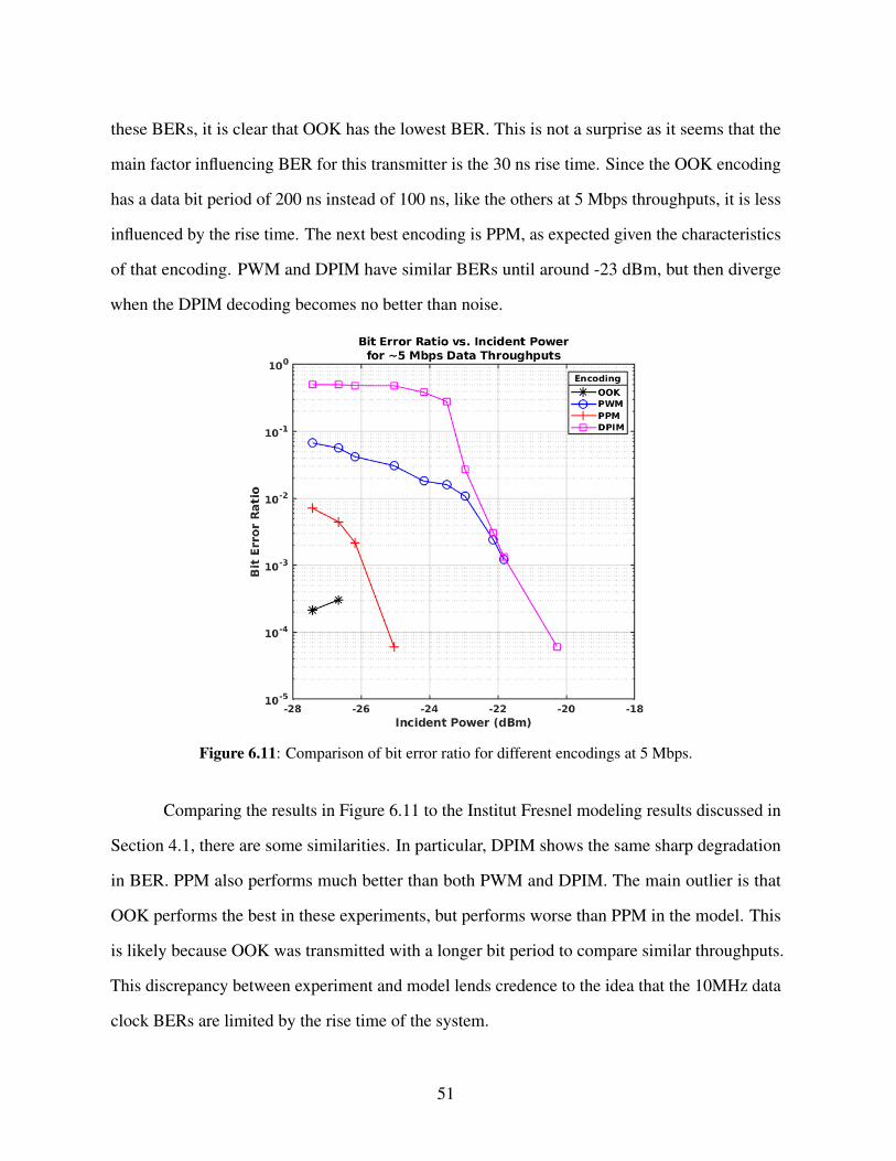
these BERs, it is clear that OOK has the lowest BER. This is not a surprise as it seems that the
main factor influencing BER for this transmitter is the 30 ns rise time. Since the OOK encoding
has a data bit period of 200 ns instead of 100 ns, like the others at 5 Mbps throughputs, it is less
influenced by the rise time. The next best encoding is PPM, as expected given the characteristics
of that encoding. PWM and DPIM have similar BERs until around -23 dBm, but then diverge
when the DPIM decoding becomes no better than noise.
Figure 6.11: Comparison of bit error ratio for different encodings at 5 Mbps.
Comparing the results in Figure 6.11 to the Institut Fresnel modeling results discussed in
Section 4.1, there are some similarities. In particular, DPIM shows the same sharp degradation
in BER. PPM also performs much better than both PWM and DPIM. The main outlier is that
OOK performs the best in these experiments, but performs worse than PPM in the model. This
is likely because OOK was transmitted with a longer bit period to compare similar throughputs.
This discrepancy between experiment and model lends credence to the idea that the 10MHz data
clock BERs are limited by the rise time of the system.
51

6.3.5 Image Series Test
The transmitted and decoded test images can be found in Figures 6.12-6.21. Figures 6.12,
6.14, 6.16, 6.18, and 6.20 show the images transmitted with an RS(255,223) error correcting code.
These are the same as the original images, with 100% of the errors being corrected, demonstrating
that the BER of 2x10⁻⁵ at -19.2 dBm is correctable using a simple RS(255,223) code. Figures
6.13, 6.15, 6.17, 6.19, and 6.21 show the same images and BER, but transmitted without any
error correcting code. Figure 6.13 is not very corrupted, with most of the features still identifiable,
but some color distortion. The rest of the images are very corrupted, with almost no identifiable
details and a large amount of color distortion. Since the performance hit of using RS(255,223) is
only 15%, transmitting at a higher bitrate with error correction is more effective at improving the
image fidelity than decreasing the throughput by 50% to use a slower throughput with a smaller
BER.
6.3.6 Video Demonstration Test
The transmitted videos can be found in Supplemental Files 2, 3, and 4. File 2 contains the
video that was transmitted at -19.2 dBm, and had a BER of 1x10⁻⁵. When viewed, this video
shows no corruption, with each frame the same as the original video. File 3 contains the video
transmitted at -20.5 dBm, and had a BER of 7.5x10⁻⁵. When viewed, this video shows corruption
only in the fourth frame. This is apparently a minor error since the subsequent frames show no
errors. File 4 contains the video transmitted at -22.2 dBm, and had a BER of 1x10⁻². When
viewed, this video shows corruption of every frame, with some worse than others. From these
results, it is estimated that the threshold for accurate video transmission is between -20 to -21
dBm for this system.
52

Figure 6.12: The first transmitted test image, RS(255,223) coded.
Figure 6.13: The first transmitted test image, with no error correction
53

Figure 6.14: The second transmitted test image, RS(255,223) coded.
Figure 6.15: The second transmitted test image, with no error correction
54

Figure 6.16: The third transmitted test image, RS(255,223) coded.
Figure 6.17: The third transmitted test image, with no error correction
55

Figure 6.18: The fourth transmitted test image, RS(255,223) coded.
Figure 6.19: The fourth transmitted test image, with no error correction
56

Figure 6.20: The fifth transmitted test image, RS(255,223) coded.
Figure 6.21: The fifth transmitted test image, with no error correction
57

6.3.7 Summary
As expected, OOK demonstrated the least data throughput reduction, while PWM and
PPM showed the most. The worst-case power draw in this system was below 2 W, with PWM
drawing 1.96 W of power. The best encoding in terms of power was PPM, with 1.19 to 1.31
W depending on the speed of transmission, with DPIM giving similar results. OOK was in the
middle of the road power-wise, having a power draw of 1.63 W to 1.77 W.
When comparing the similar throughputs around 5 Mbps, there are two different encodings
that stand out depending on the goal of the system. If the most important goal is to minimize the
BER, then the best encoding to use is OOK. However if the most important goal is to minimize
power while keeping a reasonable BER, PPM is the best option.
58

7 Evaluation of Thesis Success
The goal of this thesis was to create a modular, low-cost, low-power, and high-speed
underwater optical wireless transmitter. This chapter discusses how well this thesis accomplished
those goals.
This thesis accomplished its goal of modularity. There were three main system compo-
nents: the digital signal encoder, the driver to convert from a digital signal to an analog signal,
and the LED array. Each of these components was placed on its own PCB, and so each can be
easily swapped with another component if necessary.
This thesis accomplished its goal of being low-cost. The total cost of the transmitter was
$41.95, which is a very low cost for a device of this type. The cost can be lowered even further to
$12.95 if a project already has a processor or FPGA that can generate the encoded digital signal.
This thesis accomplished its goal of being low-power. It showed a maximum power
efficiency of 5x106 bits per Joule for the fastest encoding. The continuous power draw was a
maximum of 1.95 W for 4.7 Mbps throughput PWM, and a minimum of 1.3 W for 4.7 Mbps
throughput PPM.
This thesis accomplished its goal of being high-speed. The maximum data throughput
achieved was 8.88 Mbps. This was enough to transmit high-quality video with error-correcting
code with a frame rate of at least one frame-per-second, as was demonstrated in this thesis.
59

8 Future Work
There are several areas that could be addressed in the future to improve this system.
The transmitter hardware could be improved and a custom receiver could be created. These
improvements are outside of the scope for this thesis, but are necessary for a complete UOWC
modem.
8.1 Transmitter Hardware
The main improvement to the transmitter would be to address the large rise time. There
are several potential areas to investigate this issue.
The first is that the LEDs could be set up in series instead of in parallel. They were placed
in parallel in this project to enable the use of many LEDs without the need of two separate voltage
sources. However, this configuration could increase the capacitance created by the LEDs, and
thus increase the rise time of the LED output.
Another improvement that could be made is that the LED driver board could be laid out in
a more compact configuration, especially with the use of surface mount instead of through-hole
components. The board in this case was laid out with the goal of making the circuit easy to
understand and assemble. Also, for a production system, the power sense resistor and test points
could be removed.
60

8.2 Shrinking and Customization of Receiver Hardware
A major area that needs attention before the system can work in the field is that the
hardware for the receiver needs to be designed and validated. Ideally, there would also be work
done to make the decoding happen in real-time.
For the receiving hardware, a PIN diode could be used, setup with a transimpedance
amplifier, similar to the Thorlabs PDA used in this project. This would then feed into either a
fast ADC (at least 100 MS/s), or a voltage ladder. The digitized signal would then be fed into an
FPGA to perform the real-time matched filtering and decoding.
Another improvement would be to create an array of receivers to increase the amount of
the transmitted signal that is observed. An alternate method for increasing the observed light
would be to use a lens to focus a larger area of incident light onto the receiver surface.
61
Bibliography
[1] “SBE 25plus Sealogger CTD | Sea-Bird Scientific.” http://www.seabird.com/sbe25plus-sealogger-ctd. [Online; accessed 13-February-2018].
[2] D. Shinzaki, C. Gage, S. Tang, M. Moline, B. Wolfe, C. G. Lowe, and C. Clark, “A multi-AUV system for cooperative tracking and following of leopard sharks,” in 2013 IEEEInternational Conference on Robotics and Automation, pp. 4153–4158, May 2013.
[3] “Iver AUV: New Low Cost AUV for Coastal Applications.” http://www.iver-auv.com/index.html. [Online; accessed 13-February-2018].
[4] Z. Zeng, S. Fu, H. Zhang, Y. Dong, and J. Cheng, “A survey of underwater optical wirelesscommunications,” IEEE Communications Surveys & Tutorials, vol. 19, pp. 204–238, Q12017.
[5] N. Farr, A. Bowen, J. Ware, and C. Pontbriand, “An integrated, underwater optical/acousticcommunications system,” in OCEANS 2010 IEEE - Sydney, pp. 1–6, May 2010.
[6] “Micromodem :: Acoustic Communications Group.” https://acomms.whoi.edu/micro-modem/. [Online; accessed 13-February-2018].
[7] “Water absorption spectrum.” http://www1.lsbu.ac.uk/water/water vibrational spectrum.html. [Online; accessed 14-February-2018].
[8] C. Pontbriand, N. Farr, J. Ware, J. Preisig, and H. Popenoe, “Diffuse high-bandwidth opticalcommunications,” in OCEANS 2008, pp. 1–4, Sept 2008.
[9] H. M. Oubei, J. R. Duran, B. Janjua, H.-Y. Wang, C.-T. Tsai, Y.-C. Chi, T. K. Ng, H.-C. Kuo,J.-H. He, M.-S. Alouini, G.-R. Lin, and B. S. Ooi, “4.8 Gbit/s 16-QAM-OFDM transmissionbased on compact 450-nm laser for underwater wireless optical communication,” Opt.Express, vol. 23, pp. 23302–23309, Sep 2015.
[10] J. S. Jaffe, P. J. S. Franks, P. L. D. Roberts, D. Mirza, C. Schurgers, R. Kastner, and A. Boch,“A swarm of autonomous miniature underwater robot drifters for exploring submesoscaleocean dynamics,” Nature Communications, vol. 8, p. ncomms14189, 1 2017.
62

[11] C. Gabriel, M. Khalighi, S. Bourennane, P. Leon, and V. Rigaud, “Investigation of suitablemodulation techniques for underwater wireless optical communication,” in 2012 Interna-tional Workshop on Optical Wireless Communications (IWOW), pp. 1–3, Oct 2012.
[12] E. A. Herji, P. Andre, J. Gomes, P. Gois, and A. Pascoal, “A study of modulation formatsfor the blue ray underwater optical modem,” in 2018 Fourth Underwater Communicationsand Networking Conference (UComms), pp. 1–5, Aug 2018.
[13] P. Wang, C. Li, and Z. Xu, “A Cost-Efficient Real-Time 25 Mb/s System for LED-UOWC:Design, Channel Coding, FPGA Implementation, and Characterization,” Journal of Light-wave Technology, vol. 36, pp. 2627–2637, July 2018.
[14] M. Doniec, C. Detweiler, I. Vasilescu, M. Chitre, M. Hoffmann-Kuhnt, and D. Rus, “Aquaop-tical: A lightweight device for high-rate long-range underwater point-to-point communica-tion,” Marine Technology Society Journal, vol. 44, no. 4, 2010.
[15] M. Doniec, C. Detweiler, I. Vasilescu, and D. Rus, “Using optical communication for remoteunderwater robot operation,” in 2010 IEEE/RSJ International Conference on IntelligentRobots and Systems, pp. 4017–4022, Oct 2010.
[16] Sonardyne, BlueComm System Data Sheet, Jan 2019.
[17] J. W. Giles and I. N. Bankman, “Underwater optical communications systems. part 2:basic design considerations,” in MILCOM 2005 - 2005 IEEE Military CommunicationsConference, pp. 1700–1705 Vol. 3, Oct 2005.
[18] CREE, C503B-BCN LED Data Sheet, 2014.
[19] S. Gioux, V. Kianzad, R. Ciocan, H. S. Choi, C. Nelson, J. Thumm, R. J. Filkins, S. J.Lomnes, and J. V. Frangioni, “A low-cost linear DC - 35 MHz high-power LED driver forcontinuous wave (CW) and fluorescence lifetime imaging (FLIM),” Proc.SPIE, vol. 6848,2008.
[20] Vishay, IRLD024 Power MOSFET Data Sheet, Nov 2010. Rev. C.
[21] M. H. V. Werts, V. Raimbault, R. Texier-Picard, R. Poizat, O. Francais, L. Griscom, andJ. R. G. Navarro, “Quantitative full-colour transmitted light microscopy and dyes for con-centration mapping and measurement of diffusion coefficients in microfluidic architectures,”Lab Chip, vol. 12, pp. 808–820, 2012.
[22] ThorLabs, PDA10A Si Amplified Fixed Gain Detector User Guide, Sep 2017. Rev. J.
63