Size and shape-controlled synthesis and properties of colloidal PbSe nanocrystals
ARTICLE IN PRESS
0022-0248/$ - se
doi:10.1016/j.jc
�CorrespondE-mail addr
1Co-authors
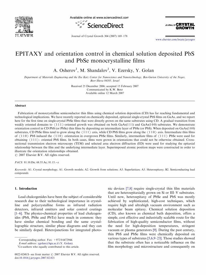
Journal of Crystal Growth 304 (2007) 169–178
www.elsevier.com/locate/jcrysgro
EPITAXY and orientation control in chemical solution deposited PbSand PbSe monocrystalline films
A. Osherov1, M. Shandalov1, V. Ezersky, Y. Golan�
Department of Materials Engineering and the Ilse Katz Center for Nanoscience and Nanotechnology, Ben-Gurion University of the Negev,
Beer-Sheva 84105, Israel
Received 25 December 2006; accepted 15 February 2007
Communicated by K.W. Benz
Available online 12 March 2007
Abstract
Fabrication of monocrystalline semiconductor thin films using chemical solution deposition (CD) has far reaching fundamental and
technological implications. We have recently reported on chemically deposited, epitaxial single-crystal PbS films on GaAs, and we report
here for the first time on single-crystal PbSe films that were directly grown on the same substrates using CD. A gradual transition from
weakly oriented domains to /1 1 1S-oriented growth was obtained on both GaAs(1 1 1) and GaAs(1 0 0) substrates. We demonstrate
orientation control in CD PbS (or PbSe) thin films by depositing an intermediate layer of PbSe (or PbS). When deposited on GaAs(1 0 0)
substrates, CD PbSe films tend to grow along the /1 1 1S axis, while CD PbS films grow along the /1 1 0S axis. Intermediate thin films
of /1 1 0S PbS induced the /1 1 0S orientation in overgrown PbSe films. Similarly, intermediate films of /1 1 1S PbSe were used for
obtaining /1 1 1S- oriented PbS films. In both cases, films were grown in orientations that could not be otherwise obtained. Cross-
sectional transmission electron microscopy (TEM) and selected area electron diffraction (ED) were used for studying the epitaxial
relationship between the film and the underlying intermediate layer. Superimposed atomic position maps were constructed in order to
illustrate the orientation relationships obtained.
r 2007 Elsevier B.V. All rights reserved.
PACS: 81.10.Dn; 68.55.Ac; 81.15.�z
Keywords: A1. Crystal morphology; A1. Growth models; A2. Growth from solutions; A3. Superlattices; A3. Heteroepitaxy; B2. Semiconducting lead
compounds
1. Introduction
Lead chalcogenides have been the subject of considerableresearch due to their technological importance in crystal-line and polycrystalline forms as infrared radiationdetectors, infrared emitters and solar control coatings[1–6]. The physico-chemical properties of lead chalcogen-ides (PbS, PbSe and PbTe) have much in common: theyhave similar chemical bonding and the same crystal-lographic structure, similar phase diagrams and they canbe similarly doped. Heterojunctions for integrated photo-
e front matter r 2007 Elsevier B.V. All rights reserved.
rysgro.2007.02.021
ing author. Fax: +9728 6472944.
ess: [email protected] (Y. Golan).
who equally contributed to this article.
nic devices [7,8] require single-crystal thin film materialsthat are heteroepitaxially grown on Si or III–V substrates.Until now, heteroepitaxy of PbSe and PbS was mostlyachieved by sophisticated, high-cost techniques, whichrequire high and ultrahigh vacuum environment such asmolecular beam epitaxy. Chemical solution deposition(CD), also known as chemical bath deposition, offers asimple, cost effective and industrially scalable route for thefabrication of high-quality semiconductor films, withoutthe need for high-deposition temperatures, stringentvacuum or plasma generators [9]. During the past century,thin PbS and PbSe films were chemically deposited onvarious types of substrates [5,6,9–23]. Those studies showedthat the substrate often has a noticeable influence on thefilm morphology and microstructure and consequently on

ARTICLE IN PRESSA. Osherov et al. / Journal of Crystal Growth 304 (2007) 169–178170
the electrical and optical properties of the layers [24,25].Variation of the deposition parameters such as temperatureand reagent concentration, allows control of the depositionreaction rates, solubility and convection and thus affect thestructural and optical properties of the resulting films.Epitaxial growth can be achieved using this method, yetless frequently than in other deposition techniques. Despitemajor progress in solution deposition of monocrystallinefilms of various superconductors in the 1990s [26], to thebest of our knowledge CD of epitaxial single-crystal PbSefilms has never been reported, and only few reports onepitaxial single-crystal PbS films have been found [19,27].The most common deposition mechanisms active in CD ofPbSe and PbS films are the cluster mechanism and the ion-by-ion mechanism. In the so-called cluster mechanism,solid clusters of the desired material, or of a certainintermediate species, are formed in solution and diffuse tothe substrate surface. Alternatively, the mechanism inwhich the chemical precursors react directly at the surfaceis known as the ion-by-ion mechanism [9]. We havepreviously shown that by varying the deposition para-meters it is possible to control the microstructure,morphology and crystallographic orientation of thin PbSe[11–13,28] and PbS [29] films deposited on various faces ofGaAs and to obtain a wide range of morphologies fromnanocrystalline to columnar grains (in the case of PbSe[11–13,28]) and monocrystalline films (in the case of PbS[29]). Those studies established the correlation between themorphological evolution and the active deposition mechan-ism [11–13,28,29].
Furthermore, we have recently showed that laser lightscattering can be effectively used in real time for monitor-ing the transition from cluster to ion-by-ion mechanism inCD of PbSe [28]. Each deposition mechanism has acharacteristic growth rate, grain size and shape, whichdirectly affect the nature and properties of the films. Hence,it was concluded that the transition from nanocrystalgrowth to columnar crystal growth occurs due to atransition from the cluster growth mechanism in the initialstages of growth to ion-by-ion growth, which is known toresult in larger crystals [11–13,23,28]. This time-dependenttransition from cluster to ion-by-ion mechanism is, in fact,expected due to depletion of lead ions in solution (e.g.increase in complex-to-metal ion concentration ratio) asthe reaction proceeds.
However, in spite of the similarity in PbS and PbSematerials, their growth tendency on GaAs is markedlydifferent. While PbS films develop with a (1 1 0)PbSJ(0 0 1)GaAs and [0 0 1]PbSJ[1 1 0]GaAs orientation relationshipwith characteristic rectangular surface faceting [29], PbSefilms grow with (1 1 1)PbSeJ(1 0 0)GaAs and ½1 1 2�PbSejj½0 1 1�GaAs and expose characteristic triangular surfacefaceting. Indeed, due to the complexity of the mechanismsin chemical deposition and several competing factors(chemical and structural) between substrate, film andsolution, it is difficult to predict a priori the effect of thesubstrate on the film orientation. Thin intermediate layers
(known also as buffer layers) are often used in order toreduce structural and thermal mismatch between thesubstrate and the overgrown layer. In heterostructuredevices, single layers or superlattice stacks are used asintermediates between the substrate and the active layer.[2,30] This allows to alleviate strain and to obtain activelayer material of superior quality. Moreover, buffer layerscan be used for controlling the orientation of thin films,consequently providing control over orientation-dependentproperties.In this paper, we show that single-crystal PbSe films can
be obtained, provided that the deposition conditions aresuch that induce the ion-by-ion deposition mechanism.Furthermore, since different orientations were obtained forchemically deposited PbSe and PbS thin films onGaAs(1 0 0) substrates [11–13,29] despite the noticeablechemical and structural similarity of these materials, wequestioned whether a thin intermediate layer of oneepilayer material can be used for controlling the orienta-tion of the other. This hypothesis has been tested in thiswork and is answered using several complementarystructural characterization techniques.
2. Experimental procedure
2.1. PbSe
Sodium sulfite (Aldrich, analytical 99.95%), seleniumpowder (Aldrich, 100 mesh, analytical 95+%), lead acetatetrihydrate (Aldrich, analytical 99+%) and potassiumhydroxide (Frutarom, analytical) were used without furtherpurification for deposition of PbSe. Films were depositedfrom a solution with a final composition of 60mMPb(CH3COO)2.3H2O, 50mM Na2SeSO3 and 0.6M KOH(complexing agent for Pb ions) at final pH 413. Stocksolution of Na2SeSO3 (0.2M) was prepared with excess ofsodium sulfite (0.5M), which was mixed with seleniumpowder in distilled water and stirred at 90 1C for 1 h. TheNa2SeSO3 solution was filtered in order to remove non-reacted selenium powder. Prior to deposition, the solutioncontained in a Pyrex beaker was purged with pure N2 for60min in order to reduce the level of dissolved O2 and CO2,and placed in the dark in a thermostatic bath to reach thedesired temperature. Growth of PbSe films on GaAs wascarried out at 30 and 40 1C for various periods of time.
2.2. PbS
Thiourea (Aldrich, ACSX99.0%), lead nitrate (Aldrich,analytical 99.99+%) and sodium hydroxide (Gadot, AR)were used without further purification for deposition ofPbS. PbS films were deposited from a solution with a finalcomposition of 0.01M PbNO3, 0.057M CS(NH2)2 and0.146M NaOH at final pH412. Fresh stock solutions of0.175M PbNO3, 1M CS(NH2)2 and 0.57M NaOH wereprepared. As for PbSe deposition, all solutions were purgedwith pure N2 for 60min in order to reduce levels of

ARTICLE IN PRESSA. Osherov et al. / Journal of Crystal Growth 304 (2007) 169–178 171
dissolved O2 and CO2. Film growth was carried out at30 1C for various periods of time in order to reach thedesired film thickness.
2.3. Substrate preparation and deposition configuration
Single-crystal GaAs(1 0 0) and GaAs(1 1 1) double-sidepolished substrates were purchased from Wafer Technol-ogy Ltd. (epi-polished, Si doped, 70.11 miscut). Substrateswere cleaved into 1� 3 cm2 rectangles and cleaned withdistilled water, then with analytical ethanol and dried.Films were deposited on the bottom face of the substratesin order to prevent large particles from adhering to thegrowing film. Therefore, the substrates were mounted on acustom-designed teflon stage at an angle of �701 withrespect to the air–solution interface.
2.4. Characterization methods
The CD films were characterized by several complemen-tary structural techniques including X-ray diffraction(XRD), field emission gun ultrahigh resolution scanning
Fig. 1. TEM bright-field images showing the microstructure of PbSe films d
GaAs(1 0 0) at 40 1C during (b) 20, (c) 40 and (d) 60min.
electron microscopy (UHR-SEM), transmission electronmicroscopy (TEM) and high-resolution transmission elec-tron microscopy (HRTEM).
XRD: The phase and orientation of the films werestudied by XRD. A Rigaku Model 2000 Diffractometeroperating in the y/2y geometry using Cu Ka radiation,l ¼ 1.5405 A was used at 40 kV and 30mA. Scans were runin a 2y range of 201–571 in 0.021 steps with intervals of11/min for PbSe films and in a 2y range of 201–601 in 0.021steps for PbS.
FEG-SEM: The morphology of the films was observedusing an ultrahigh resolution JEOL JSM-7400F FEG-SEMwithout coating. Acceleration voltages ranged from 1 to5 kV. Film thickness was measured from cross-sectionswhile surface topography was observed in plan view.
TEM: TEM and HRTEM were carried out using aJEOL JEM-2010 instrument operating at 200 kV and FEITecnai G2 instrument operating at 120 kV. Film thicknesswas measured from the TEM cross-sections. Selected areaelectron diffraction (SAED) patterns were obtained bypositioning the selected area diffraction aperture of theTEM over the desired area of the film and/or substrate.
eposited on Ga face of GaAs(1 1 1) at 50 1C during 30min (a) and on

ARTICLE IN PRESSA. Osherov et al. / Journal of Crystal Growth 304 (2007) 169–178172
3. Results
3.1. PbSe single-crystal growth
Single-crystal PbSe(1 1 1) films were obtained on Ga faceof GaAs(1 1 1) substrate (Fig. 1a). Electron diffraction(ED) confirmed the monocrystalline nature of the film(Figs. 2a and b). The ED patterns were taken at variouszone axes within the limits of sample tilting in the TEM inorder to reassure the single-crystal structure of the films.The ED indicated a rather expected epitaxial orientationrelationship (1 1 1)PbSeJ(1 1 1)GaAs , ½1 1 2�PbSejj½1 1 2�GaAs, inagreement with the orientation we have previously reportedfor polycrystalline CBD PbSe films on GaAs(1 1 1) sub-strates [12]. A more complicated case of epitaxy wasobserved when PbSe was deposited on GaAs(1 0 0) sub-strate. ED at various zone axes again confirmed the single-crystal nature of the films, with a more unusual epitaxialorientation relationship in which (1 1 1)PbSeJ(1 0 0)GaAs ,½1 1 2�PbSejj½1 1 0�GaAs, with the GaAs substrate. Cross-sectional TEM was carried out in order to monitor theevolution of the film morphology. The TEM images shownin Figs. 1b–d demonstrate the microstructure and morphol-ogy evolution of the films deposited at 40 1C during 20, 40and 60min, respectively. The sample deposited for 20min
Fig. 2. (a) SAED pattern taken from both film and a substrate of PbSe film
presentation of the diffraction pattern with hkl indices, where the PbSe½1 1 2� z
film deposited on GaAs(1 0 0) at 40 1C for 40min. (d) Schematic presentation o
parallel to the GaAs½1 1 0� zone axis.
showed very small pyramids on the surface, with a filmthickness of 220nm (Fig. 1b). The image indicates thepresence of two regions in the film. Near the GaAs/PbSeinterface there is a discontinuous polycrystalline structure ofsmall crystallites with a typical size of 50 nm. Small arcs inSAED pattern of this sample confirmed the initiallypolycrystalline structure of this layer (not shown). Abovethis layer, a monocrystalline region with small-angledomains is observed. The film deposited during 40minwas thicker (580 nm) and showed large facets thatconfirmed the surface structure obtained in SEM images(shown later in Fig. 4), as well as small-angle domainswithin the film, shown in Fig. 1c. The sample deposited for60min showed a 1mm thick film with a very smooth surface(Fig. 1d). SAED pattern of 40min sample (SAED of 60minsample was identical) readily confirmed its monocrystallinenature (Figs. 2c and d).XRD spectra of the films deposited at 40 1C for
increasing periods of time are shown in Fig. 3a. The dataindicate the presence of single-phase PbSe films, with allreflections corresponding to rocksalt PbSe (JCPDS powderdiffraction file ]6�354). In the beginning of the deposition(film deposited for 10min) a strong (1 1 1) preferredorientation is observed, although the (2 0 0) peak can stillbe detected. With increasing deposition time, the intensity
deposited on Ga face of GaAs(1 1 1) at 50 1C for 30min. (b) Schematic
one axis is parallel to the GaAs½1 1 2� zone axis. (c) SAED pattern of PbSe
f the diffraction pattern with hkl indices, where the PbSe½1 1 2� zone axis is
ARTICLE IN PRESS
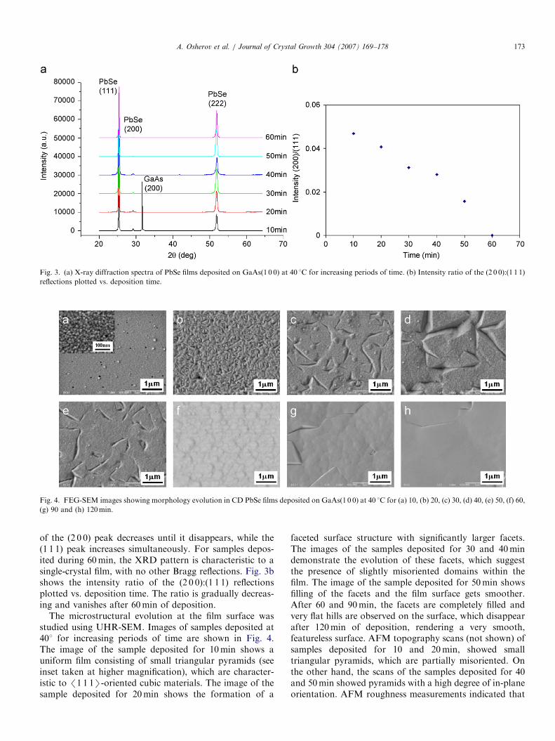
Fig. 3. (a) X-ray diffraction spectra of PbSe films deposited on GaAs(1 0 0) at 40 1C for increasing periods of time. (b) Intensity ratio of the (2 0 0):(1 1 1)
reflections plotted vs. deposition time.
Fig. 4. FEG-SEM images showing morphology evolution in CD PbSe films deposited on GaAs(1 0 0) at 40 1C for (a) 10, (b) 20, (c) 30, (d) 40, (e) 50, (f) 60,
(g) 90 and (h) 120min.
A. Osherov et al. / Journal of Crystal Growth 304 (2007) 169–178 173
of the (2 0 0) peak decreases until it disappears, while the(1 1 1) peak increases simultaneously. For samples depos-ited during 60min, the XRD pattern is characteristic to asingle-crystal film, with no other Bragg reflections. Fig. 3bshows the intensity ratio of the (2 0 0):(1 1 1) reflectionsplotted vs. deposition time. The ratio is gradually decreas-ing and vanishes after 60min of deposition.
The microstructural evolution at the film surface wasstudied using UHR-SEM. Images of samples deposited at401 for increasing periods of time are shown in Fig. 4.The image of the sample deposited for 10min shows auniform film consisting of small triangular pyramids (seeinset taken at higher magnification), which are character-istic to /1 1 1S-oriented cubic materials. The image of thesample deposited for 20min shows the formation of a
faceted surface structure with significantly larger facets.The images of the samples deposited for 30 and 40mindemonstrate the evolution of these facets, which suggestthe presence of slightly misoriented domains within thefilm. The image of the sample deposited for 50min showsfilling of the facets and the film surface gets smoother.After 60 and 90min, the facets are completely filled andvery flat hills are observed on the surface, which disappearafter 120min of deposition, rendering a very smooth,featureless surface. AFM topography scans (not shown) ofsamples deposited for 10 and 20min, showed smalltriangular pyramids, which are partially misoriented. Onthe other hand, the scans of the samples deposited for 40and 50min showed pyramids with a high degree of in-planeorientation. AFM roughness measurements indicated that

ARTICLE IN PRESSA. Osherov et al. / Journal of Crystal Growth 304 (2007) 169–178174
flat 1� 1 mm areas of the sample deposited for 120minwere atomically smooth.
3.2. PbS and PbSe orientation control by intermediate
layers
An XRD spectrum of PbS on GaAs(1 0 0) grown ona pre-deposited intermediate layer of PbSe is shown inFig. 5a. The spectrum confirms the presence of the rocksaltcrystalline form of the two lead chalcogenide materials: Amain film of PbS (JCPDS file ]5�592), with strong /1 1 1Spreferred orientation which is induced by the PbSeintermediate layer (JCPDS file ]6–354). Alternatively,Fig. 5b shows the XRD spectrum of PbSe deposited onan intermediate layer of /1 1 0S-oriented PbS thin film
Fig. 5. (a) XRD pattern of PbS grown at 30 1C for 60min in the presence
of a PbSe intermediate layer grown at 30 1C for 20min on GaAs(1 0 0).
The pattern indicates the presence of a PbSe film with /1 1 1S texture and
epitaxial growth of PbS film on top of the PbSe layer. (b) XRD pattern of
PbSe grown at 30 1C for 60min in the presence of a PbS intermediate layer
grown at 30 1C for 20min on GaAs(1 0 0). The pattern indicates the
presence of a PbS film with /1 1 0S texture and epitaxial growth of a PbSe
film on top of the PbS layer.
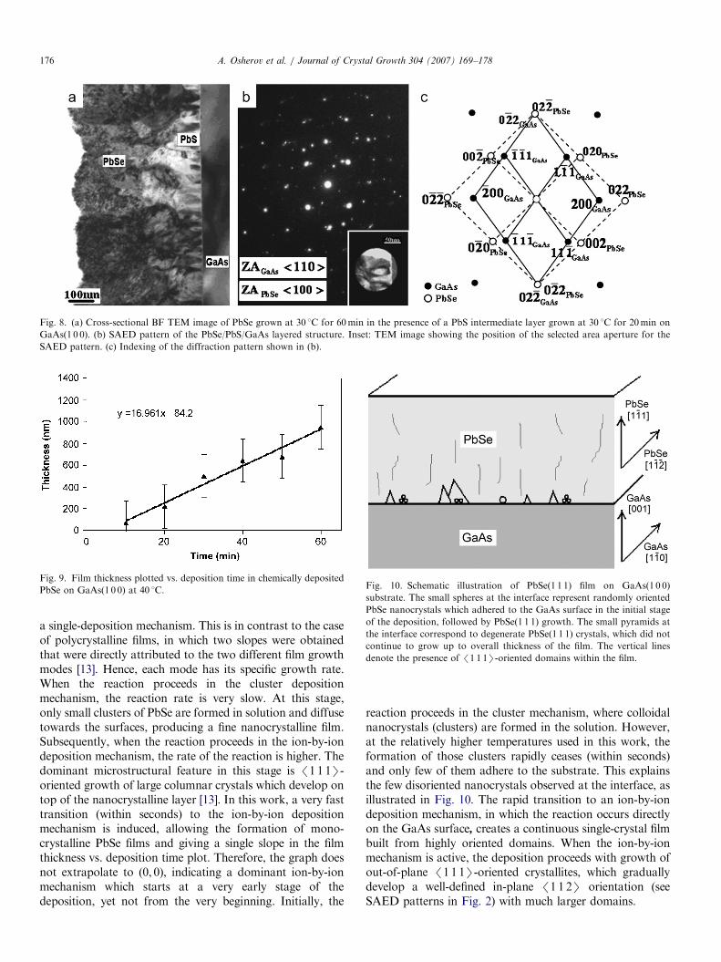
that was pre-deposited on the GaAs(1 0 0) substrate. Thespectrum indicates that the overgrown PbSe layer repeatsthe orientation of the PbS intermediate film. The absenceof any other diffraction peaks indicates that no othercrystalline phases, such as oxides or carbonates of Pb, existwith detectable concentration within the layers. Note thatthe region 2y ¼ 311–341 was not scanned in both spectradue to the presence of an intense 200GaAs single-crystalsubstrate reflection. Fig. 6a shows a secondary electronUHR-SEM image of a PbSe film deposited on GaAs(1 0 0).The image indicates triangular pyramidal facets character-istic of /1 1 1S-oriented crystals with {1 0 0}-type facetsexposed. The image of the PbS film deposited directly ontop of this layer (Fig. 6b) confirms that the PbS film clearlyfollows the orientation of the previously deposited PbSeintermediate layer, in agreement with the XRD data inFig. 5a. Similarly, the UHR-SEM micrograph of a PbSfilm deposited on GaAs(1 0 0) substrate shown in Fig. 6cindicates a rectangular-faceted morphology characteristicto /1 1 0S-oriented films, with {1 0 0}-type facets exposedat 451 to the growth axis (to the surface normal), whileFig. 6d shows a PbSe layer deposited on top of the PbSintermediate layer shown in Fig. 6c. The image shows asimilar rectangular-faceted morphology and confirms thatthe PbSe film follows the orientation of the previouslydeposited PbS intermediate layer, in agreement with theXRD data shown in Fig. 5b. The cross-sectional dark field(DF) TEM image shown in Fig. 7a demonstrates themicrostructure of a 500 nm thick PbSe/PbS layeredstructure. The image was generated from the 111PbSreflection (which cannot be distinguished from the corre-sponding 111PbSe reflection due to their close proximity).The two regions of this structure can be distinguished. Theintermediate layer close to the GaAs(1 0 0) surface is about150 nm thick and comprised of columnar PbSe nanocrys-tallites that are /1 1 1S oriented relative to the GaAssubstrate. Above this there is a thicker layer consisting ofPbS crystallites that follow the underlying PbSe orienta-tion. Epitaxy was confirmed by SAED as shown in Fig. 7b,indicating a (1 1 1)PbSeJ(1 0 0)GaAs , ½1 1 2�PbSejj½0 1 1�GaAs
and (1 1 1)PbSJ(1 1 1)PbSe , ½1 1 1�PbSjj½0 1 1�PbSe orientationrelationship between the layers. A schematic representationshowing the indexing of the diffraction pattern in Fig. 7b isshown in Fig. 7c. The cross-sectional bright field (BF)TEM image shown in Fig. 8a demonstrates the micro-structure of the dense, continuous PbSe films obtained onthe top of an intermediate PbS layer previously depositedon the GaAs(1 0 0) substrate. The two different regions ofthe PbS/PbSe structure are evident. The �100 nm thickPbS intermediate layer is comprised of columnar crystal-lites that are /1 1 0S oriented with respect to theGaAs(1 0 0) substrate. Above this there is a 400 nm thickPbSe layer, which follows the orientation and morphologyof the underlying PbS film. The SAED pattern in Fig. 8bwas taken from the region (f ¼ 200 nm) shown in the insetin Fig. 8. The diffraction indicates a (1 1 0)PbSJ(0 0 1)GaAs,[0 0 1]PbSJ[1 1 0]GaAs and (1 1 0)PbSeJ(1 1 0)PbS, [0 0 1]PbSeJ

ARTICLE IN PRESS
Fig. 6. Secondary electron UHR-SEM images of: (a) PbSe deposited on GaAs(1 0 0) substrate at 30 1C for 30min. The triangular pyramids are typical for
a /1 1 1S-oriented film, (b) PbS grown on the PbSe intermediate layer shown in (a) at 30 1C for 60min, (c) PbS deposited on GaAs(1 0 0) at 30 1C for
20min, showing rectangular pyramids that are typical to the /1 1 0S orientation and (d) PbSe film grown at 30 1C for 60min on top of the PbS
intermediate layer shown in (c).
Fig. 7. (a) Cross-sectional DF TEM image generated from the 111PbS reflection, (b) SAED of the PbS/PbSe/GaAs layered structure and (c) indexing of the
diffraction pattern shown in (b).
A. Osherov et al. / Journal of Crystal Growth 304 (2007) 169–178 175
[0 0 1]PbS orientation relationship between the layers.A schematic representation showing the indexing of thereflections of the diffraction pattern obtained in Fig. 8bis presented in Fig. 8c. Note that due to the proximityof the PbS and PbSe reflections, the PbS reflectionsobtained from the intermediate layer are not indicated inFig. 8c.
4. Discussion
4.1. PbSe single-crystal growth
The plot in Fig. 9 shows a linear dependence of the filmthickness on deposition time. Such single slope behaviorfrom an early stage in film growth indicates the existence of
ARTICLE IN PRESS
Fig. 8. (a) Cross-sectional BF TEM image of PbSe grown at 30 1C for 60min in the presence of a PbS intermediate layer grown at 30 1C for 20min on
GaAs(1 0 0). (b) SAED pattern of the PbSe/PbS/GaAs layered structure. Inset: TEM image showing the position of the selected area aperture for the
SAED pattern. (c) Indexing of the diffraction pattern shown in (b).
Fig. 9. Film thickness plotted vs. deposition time in chemically deposited
PbSe on GaAs(1 0 0) at 40 1C. Fig. 10. Schematic illustration of PbSe(1 1 1) film on GaAs(1 0 0)
substrate. The small spheres at the interface represent randomly oriented
PbSe nanocrystals which adhered to the GaAs surface in the initial stage
of the deposition, followed by PbSe(1 1 1) growth. The small pyramids at
the interface correspond to degenerate PbSe(1 1 1) crystals, which did not
continue to grow up to overall thickness of the film. The vertical lines
denote the presence of /1 1 1S-oriented domains within the film.
A. Osherov et al. / Journal of Crystal Growth 304 (2007) 169–178176
a single-deposition mechanism. This is in contrast to the caseof polycrystalline films, in which two slopes were obtainedthat were directly attributed to the two different film growthmodes [13]. Hence, each mode has its specific growth rate.When the reaction proceeds in the cluster depositionmechanism, the reaction rate is very slow. At this stage,only small clusters of PbSe are formed in solution and diffusetowards the surfaces, producing a fine nanocrystalline film.Subsequently, when the reaction proceeds in the ion-by-iondeposition mechanism, the rate of the reaction is higher. Thedominant microstructural feature in this stage is /1 1 1S-oriented growth of large columnar crystals which develop ontop of the nanocrystalline layer [13]. In this work, a very fasttransition (within seconds) to the ion-by-ion depositionmechanism is induced, allowing the formation of mono-crystalline PbSe films and giving a single slope in the filmthickness vs. deposition time plot. Therefore, the graph doesnot extrapolate to (0, 0), indicating a dominant ion-by-ionmechanism which starts at a very early stage of thedeposition, yet not from the very beginning. Initially, the
reaction proceeds in the cluster mechanism, where colloidalnanocrystals (clusters) are formed in the solution. However,at the relatively higher temperatures used in this work, theformation of those clusters rapidly ceases (within seconds)and only few of them adhere to the substrate. This explainsthe few disoriented nanocrystals observed at the interface, asillustrated in Fig. 10. The rapid transition to an ion-by-iondeposition mechanism, in which the reaction occurs directlyon the GaAs surface, creates a continuous single-crystal filmbuilt from highly oriented domains. When the ion-by-ionmechanism is active, the deposition proceeds with growth ofout-of-plane /11 1S-oriented crystallites, which graduallydevelop a well-defined in-plane /1 1 2S orientation (seeSAED patterns in Fig. 2) with much larger domains.

ARTICLE IN PRESSA. Osherov et al. / Journal of Crystal Growth 304 (2007) 169–178 177
4.2. PbS and PbSe orientation control by intermediate
layers
Despite of the noticeable similarity between PbS andPbSe, CD films of these two materials showed verydifferent orientation relations with the underlyingGaAs(1 0 0) substrate (as described in the first part of thiswork for PbSe and in Ref. [29] for PbS epilayers). There areboth chemical and structural factors that are likely tocontribute to this pronounced difference. The different
Fig. 11. Superimposed atomic position maps (a) PbSe(0 0 1) on GaAs(00 1), with
, (c) PbSeð1 1 1Þ on GaAs(001), with [1 1 0]PbSeJ[1 1 0]GaAs and ½1 2 1�PbSejj½1 1
½1 1 0�PbSjj½1 1 0�GaAs. Maps (a,b) represent hypothetical cases of conventional epi
this study. Hexagons indicate the position of the Ga (or As) atoms, stars indica
anion precursors (thiourea vs. selenosulfate), differentcounter anions in the lead salt used (nitrate vs. acetate)and different monovalent cations (Na+ vs. K+ ) present athigh concentrations most reasonably lead to differentadsorption characteristics which are likely to be specific fordifferent crystallographic planes in the rocksalt structure.On the other hand, the differences in size between S and Seanions affect the lattice constants and consequently lead todifferent lattice mismatch with the GaAs substrate. Themismatch f ¼ ða0ðsubstrateÞ � a0ðfilmÞÞ=a0ðfilmÞ gives 7.68
[1 0 0]PbSeJ[1 0 0]GaAs, (b) PbS(0 01) on GaAs(00 1), with [1 0 0]PbSJ[1 0 0]GaAs
0�GaAs and (d) PbS(110) on GaAs(001), with [0 0 1]PbSJ[1 1 0]GaAs and
taxy, while maps (c, d) represent the actual orientation relations obtained in
te position of Pb atoms and dots indicate position of S or Se atoms.

ARTICLE IN PRESSA. Osherov et al. / Journal of Crystal Growth 304 (2007) 169–178178
and 4.75% for PbSe on GaAs and PbS on GaAs,respectively. The fairly large f values can explain the factthat the straightforward (1 0 0)filmJ(1 0 0)substrate orientationrelationship is not observed in neither case. This hypothe-tical case is shown in Figs. 11a and b for PbSe onGaAs(1 0 0) and PbS on GaAs(1 0 0), respectively. Thesuperimposed atomic position images for the conventionalcases of epitaxy show that, as expected, larger regions oflattice match are observed for PbS and smaller regions forPbSe, due to the better fit in lattice parameters betweenPbS and GaAs. On the other hand, the superimposedatomic position maps corresponding to the unconventionalorientation relations obtained in this work for PbSe andPbS on GaAs(1 0 0) are shown in Figs. 11c and d ,respectively. The image representing the case of PbSeð1 1 1Þon GaAs(0 0 1), with [1 1 0]PbSeJ[1 1 0]GaAs and ½1 2 1�PbSejj½1 1 0�GaAs is shown in Fig. 11c. The situation describing theorientation of CD PbS(1 1 0) on GaAs(0 0 1) is shown inFig. 11d, with [0 0 1]PbSJ[1 1 0]GaAs and ½1 1 0�PbSjj½1 1 0�GaAs.While the former case (PbSe/GaAs) shows a uniforminterface across the entire area, the latter case (PbS/GaAs)shows bands of varying lattice match in this orientationrelationship. The insets in Fig. 11 represent larger area (de-magnified) versions of each map, which clearly demon-strate the differences between the two orientations. Thesuperimposed pattern suggests a more uniform andcoherent interface, which can explain the occurrence ofthe orientation relations obtained for PbSe and PbS onGaAs(1 0 0). For the case of PbS, one may speculate thatthis rather unusual orientation relationship could befavored due to a close lattice match (less than 1%) in the3:2 superstructure formed between 3�d{1 1 0}GaAS and2�d{1 0 0}PbS, similar to that previously reported forepitaxial CdSe on Au(1 1 1) [31]. This unexpected orienta-tion is currently under further investigation using HRTEMand HRTEM simulations. It should be noted thatWatanabe and Mita [15] reported similar unexpectedbehavior for PbS on wurtzite CdS substrates. In contrastwith growth on GaAs(1 0 0), growth of PbS on PbSe (andvice versa) results in complete repetition of the orientationfrom the substrate (or, in this case, from the intermediatelayer) to overgrown film, despite the fairly large (ca. 5%)mismatch between PbS and PbSe. In this case, the chemicaland structural similarity between these two materialsallows for a conventional epitaxial orientation relationship.
5. Conclusions
In summary, we have found that both depositiontemperature and deposition time play a major role inobtaining monocrystalline PbSe films. By increasing thedeposition temperature to 40 1C or higher, a very fast
transition to the ion-by-ion deposition mechanism isobtained, allowing the formation of monocrystalline PbSefilms. The domain size increases with film thickness,resulting in single-crystal films with fewer defects. At thefinal stage, the deposition proceeds as pure single-crystal
growth with an atomically smooth surface (Fig. 10). Inaddition, we have showed that chemical deposition of PbSfilms follows the orientation of an underlying PbSe layerand vice versa. These studies can open the way for thefabrication of layered superlattice structures using CD.Furthermore, control over the microstructure of the layers(from nanocrystalline to single crystals) [11–13,29] can beused for tuning the opto-electronic characteristics of thesuperlattice structures obtained.
Acknowledgment
This work has been partially supported by the EuropeanCommission FP-6 project SEMINANO under Contractno. NMP4-CT-2004-505285.
References
[1] P.K. Nair, M.T.S. Nair, A. Fernandez, M. Ocampo, J. Phys. D:
Appl. Phys. 22 (1989) 829.
[2] P. Capper, C.T. Eliot, Infrared Detectors and Emitters: Materials and
Devices, Kluver Academic Publishers, 2001.
[3] P.K. Nair, M.T.S. Nair, J. Phys. D: Appl. Phys. 23 (1990) 150.
[4] P.K. Nair, M. Ocampo, A. Fernandez, M.T.S. Nair, Sol. Energy
Mater. 20 (1990) 235.
[5] K.D. Dobson, G. Hodes, Y. Mastai, Sol. Energy Mater. Sol. Cells 80
(2003) 283.
[6] H. Elabd, A.J. Steckl, J. Appl. Phys. 51 (1) (1980) 726.
[7] H. Zogg, S. Blunier, C. Marssin, J. Mazek, A.N. Tiwari, IEEE Trans.
Electron Dev. 38 (1991) 1110.
[8] H.Z. Wu, X.M. Fang, R. Salas, J.D. McAllister, P.J. McCann,
J. Vac. Sci. Technol. B17 (1999) 1263.
[9] G. Hodes, Chemical Solution Deposition of Semiconductor Films,
M. Dekker, New York, 2003.
[10] M. Froment, H. Cachet, H. Essaadi, G. Maurin, R. Cortes, Pure
Appl. Chem. 9 (1997) 77.
[11] M. Shandalov, Y. Golan, Eur. Phys. J. Appl. Phys. 24 (2003) 13.
[12] M. Shandalov, Y. Golan, Eur. Phys. J. Appl. Phys. 28 (2004) 51.
[13] M. Shandalov, Y. Golan, Eur. Phys. J. Appl. Phys. 31 (2005) 27.
[14] J.J. Valenzuela-Jauregui, R. Ramirez-Bon, A. Mendoza-Galvan,
M. Sotelo-Lerma, Thin Solid Films 441 (2003) 104.
[15] S. Watanabe, Y. Mita, J. Electrochem. Soc. 116 (1969) 989.
[16] I. Pop, C. Nascu, V. Ionescu, E. Indrea, I. Bratu, Thin Solid Films
307 (1997) 240.
[17] H. Elabd, A.J. Steckl, W. Vidinski, Sol. Cells 1 (1980) 199.
[18] Y.S. Sarma, H.N. Acharya, N.K. Misra, J. Mater. Sci. 21 (1986) 137.
[19] M. Isshiki, T. Endo, K. Masumoto, J. Electrochem. Soc. 137 (9)
(1990) 2697.
[20] M.K. Norr, J. Phys. Chem. 65 (1961) 1278.
[21] S. Gorer, A. Albu-Yaron, G. Hodes, Chem. Mater. 7 (1995) 1243.
[22] S. Gorer, G. Hodes, J. Phys. Chem. 98 (1994) 5338.
[23] S. Gorer, A. Albu-Yaron, G. Hodes, J. Phys. Chem. 99 (1995) 16442.
[24] G.H. Blount, P.J. Schreiber, D.K. Smith, R.T. Tamada, J. Appl.
Phys. 44 (1973) 978.
[25] E.M. Larramendi, O. Calzadilla, A. Gonzalez-Arias, E. Hernandez,
J. Ruiz-Garcia, Thin Solid Films 389 (2001) 301.
[26] F.F. Lange, Science 273 (1996) 903.
[27] J.L. Davis, M.K. Norr, J. Appl. Phys. 37 (1966) 1670.
[28] M. Shandalov, Y. Golan, Chem. Mater. 18 (2006) 3593.
[29] A. Osherov, V. Ezersky, Y. Golan, Eur. Phys. J. Appl. Phys. 37 (2007) 39.
[30] D. Khokholov, Lead Chalcogemides Physics and Applications,
Vol. 18, Taylor&Francis, New York, London, 2003.
[31] Y. Golan, L. Margulis, I. Rubinstein, G. Hodes, Langmuir 8 (1992)
749.
Copyright © 2022 FDOKUMEN