The mechanism of sputter-induced epitaxy modification in YBCO (001) films grown on MgO (001)...
11
The mechanism of sputter-induced epitaxy modification in YBCO (001) films grown on MgO (001) substrates Y. Huang, B. V. Vuchic, M. Carmody, P. M. Baldo, and K. L. Merkle Materials Science Division, Argonne National Laboratory, Argonne, Illinois 60439 D. B. Buchholz, S. Mahajan, J. S. Lei, P. R. Markworth, R. P. H. Chang, and L. D. Marks Department of Materials Science and Engineering, Northwestern University, Evanston, Illinois 60201 (Received 9 July 1997; accepted 25 January 1998) The sputter-induced epitaxy change of in-plane orientation occurring in YBa 2 Cu 3 O 72x (001) thin films grown on MgO (001) substrates by pulsed organo-metallic beam epitaxy (POMBE) is investigated by a series of film growth and characterization experiments, including RBS and TEM. The factors influencing the orientation change are systematically studied. The experimental results suggest that the substrate surface morphology change caused by the ion sputtering and the Ar ion implantation in the substrate surface layer are not the major factors that affect the orientation change. Instead, the implantation of W ions, which come from the hot filament of the ion gun, and the initial Ba deposition layer in the YBCO film growth play the most important roles in controlling the epitaxy orientation change. Microstructure studies show that a Ba x Mg 12x O buffer layer is formed on top of the sputtered substrate surface due to Ba diffusion into the W implanted layer. It is believed that the formation of this buffer layer relieves the large lattice mismatch and changes the YBCO film from the 45 ± oriented growth to the 0 ± oriented growth. I. INTRODUCTION Grain boundary junctions in high-T c superconductor materials have attracted much attention in recent years. Many methods have been developed to fabricate grain boundary junctions (GBJ’s). Among others, the step edge method, 1,2 bicrystal method, 3–5 and biepitaxy method 6,7 have been extensively studied. Junctions made by the bicrystal method are presently being used in commercial devices. The disadvantage of these fabrication processes is that they are all quite complex and/or expensive. Therefore there is a need for simpler and inexpensive procedures. The method to be discussed in this paper is similar to but much simpler than the biepitaxy tech- nique. This method uses low-energy ion sputtering to selectively treat the substrates. Under specific synthesis conditions the superconductor films grow with different in-plane orientations on the sputtered and nonsputtered substrate areas and thus form GBJ’s between the two areas. The change of epitaxy orientation by ion sputtering will be termed “sputter-induced epitaxy modification” (SIEM) and the method to form GBJ’s by this change, the SIEM method. The SIEM phenomenon was first observed by Chew et al. 8 They grew c-axis normal YBa 2 Cu 3 O 72x (YBCO) films on MgO (001) substrates by the coevaporation method. On nonsputtered substrates they observed the in- plane orientation relation to be [100] YBCO yy[100] MgO , but on substrate sputtered by low energy Ar ions at ,200 ± C, the orientation relation became [110] YBCO yy[100] MgO . Thus, the YBCO film assumed a 45 ± rotation of in-plane rotation on sputtered substrates. It should be noted that Chew et al. were not able to reproduce their results after making variations to their processing chamber. 9 Vuchic et al. 10 observed the same type of orientation change in the YBCO films grown on MgO (001) by pulsed organo- metallic beam epitaxy (POMBE). Using the sputter- induced epitaxial rotation Vuchic et al. fabricated 45 ± GBJ’s and systematically investigated the microstructure and electrical properties of the junctions. 11,12 To be concise, hereafter we refer to the in-plane ori- entation relations by the angle between the YBCO [100] and MgO [100]. Hence, in this notation the orientation relation [100] YBCO yy[100] MgO (sometimes called cube- on-cube) is a “0 ± orientation” and [110] YBCO yy[100] MgO is a “45 ± orientation.” Relative to these early observations, Buchholz et al. recently reported different YBCOyMgO orientation re- lations in films grown by the POMBE method: Under standard synthesis conditions the YBCO films on the nonsputtered MgO regions are 45 ± oriented and those on the sputtered regions are 0 ± oriented. 13 The result is verified by several experimental methods and can be routinely reproduced. It is believed that the difference from previous results was caused by some unknown changes in the processing chamber and by paying par- ticular attention to the deposition of the initial atomic layers. It is evident that the factors that affect the YBCO growth orientation on MgO (100) are quite complex and the task for controlling the orientation by ion sputtering is not simple. In order to understand the factors involved 3378 J. Mater. Res., Vol. 13, No. 12, Dec 1998 1998 Materials Research Society Help Comments Welcome Journal of MATERIALS RESEARCH
-
Upload
independent -
Category
Documents
-
view
8 -
download
0
Transcript of The mechanism of sputter-induced epitaxy modification in YBCO (001) films grown on MgO (001)...

ly
It
3378
HelpCommentsWelcomeJournal of
MATERIALS RESEARCH
The mechanism of sputter-induced epitaxy modificationin YBCO (001) films grown on MgO (001) substratesY. Huang, B. V. Vuchic, M. Carmody, P. M. Baldo, and K. L. MerkleMaterials Science Division, Argonne National Laboratory, Argonne, Illinois 60439
D. B. Buchholz, S. Mahajan, J. S. Lei, P. R. Markworth, R. P. H. Chang, and L. D. MarksDepartment of Materials Science and Engineering, Northwestern University, Evanston, Illinois 60201
(Received 9 July 1997; accepted 25 January 1998)
The sputter-induced epitaxy change of in-plane orientation occurring in YBa2Cu3O72x
(001) thin films grown on MgO (001) substrates by pulsed organo-metallic beam epitaxy(POMBE) is investigated by a series of film growth and characterization experiments,including RBS and TEM. The factors influencing the orientation change are systematicalstudied. The experimental results suggest that the substrate surface morphology changecaused by the ion sputtering and the Ar ion implantation in the substrate surface layerare not the major factors that affect the orientation change. Instead, the implantation ofW ions, which come from the hot filament of the ion gun, and the initial Ba depositionlayer in the YBCO film growth play the most important roles in controlling the epitaxyorientation change. Microstructure studies show that a BaxMg12xO buffer layer is formedon top of the sputtered substrate surface due to Ba diffusion into the W implanted layer.is believed that the formation of this buffer layer relieves the large lattice mismatch andchanges the YBCO film from the 45± oriented growth to the 0± oriented growth.
ag
ti
eivp
t
rtwin”e
o
thatter
ino-r-
ure
ri-00]on-
erthe
becewnpar-icO
ndged
I. INTRODUCTION
Grain boundary junctions in high-Tc superconductormaterials have attracted much attention in recent yeaMany methods have been developed to fabricate grboundary junctions (GBJ’s). Among others, the step edmethod,1,2 bicrystal method,3–5 and biepitaxy method6,7
have been extensively studied. Junctions made bybicrystal method are presently being used in commercdevices. The disadvantage of these fabrication procesis that they are all quite complex and/or expensivTherefore there is a need for simpler and inexpensprocedures. The method to be discussed in this pais similar to but much simpler than the biepitaxy technique. This method uses low-energy ion sputteringselectively treat the substrates. Under specific syntheconditions the superconductor films grow with differenin-plane orientations on the sputtered and nonsputtesubstrate areas and thus form GBJ’s between theareas. The change of epitaxy orientation by ion sputterwill be termed “sputter-induced epitaxy modification(SIEM) and the method to form GBJ’s by this changthe SIEM method.
The SIEM phenomenon was first observed by Cheet al.8 They grewc-axis normal YBa2Cu3O72x (YBCO)films on MgO (001) substrates by the coevaporatimethod. On nonsputtered substrates they observed theplane orientation relation to be [100]YBCOyy[100]MgO, buton substrate sputtered by low energy Ar ions at,200 ±C,the orientation relation became [110]YBCOyy[100]MgO.Thus, the YBCO film assumed a 45± rotation of in-plane
J. Mater. Res., Vol. 13, No. 12, Dec 1998
rs.ine
healses.eer
-osistedog
,
w
nin-
rotation on sputtered substrates. It should be notedChewet al. were not able to reproduce their results afmaking variations to their processing chamber.9 Vuchicet al.10 observed the same type of orientation changethe YBCO films grown on MgO (001) by pulsed organmetallic beam epitaxy (POMBE). Using the sputteinduced epitaxial rotation Vuchicet al. fabricated 45±
GBJ’s and systematically investigated the microstructand electrical properties of the junctions.11,12
To be concise, hereafter we refer to the in-plane oentation relations by the angle between the YBCO [1and MgO [100]. Hence, in this notation the orientatirelation [100]YBCOyy[100]MgO (sometimes called cubeon-cube) is a “0± orientation” and [110]YBCOyy[100]MgO
is a “45± orientation.”Relative to these early observations, Buchholzet al.
recently reported different YBCOyMgO orientation re-lations in films grown by the POMBE method: Undstandard synthesis conditions the YBCO films onnonsputtered MgO regions are 45± oriented and thoseon the sputtered regions are 0± oriented.13 The resultis verified by several experimental methods and canroutinely reproduced. It is believed that the differenfrom previous results was caused by some unknochanges in the processing chamber and by payingticular attention to the deposition of the initial atomlayers. It is evident that the factors that affect the YBCgrowth orientation on MgO (100) are quite complex athe task for controlling the orientation by ion sputterinis not simple. In order to understand the factors involv
1998 Materials Research Society

Y. Huang et al.: The mechanism of sputter-induced epitaxy modification in YBCO (001) films
se
n
enwy
rnn
tyd
s
y
s
e
b
t
f
n
ea
m
tes-
ea
n
le
d
gyee,,by
t
nt--
m
y
is.
ton
ns.p
e
and reproducibly control the growth orientation it iessential to know the mechanism of the sputter-inducepitaxy modification. This is important not only forfurther improvement of the GBJ quality, but also for extension of the SIEM method to other systems of differefilm/substrate combinations and/or synthesis routes.
Before we discuss the mechanism of SIEM, a brireview of the previous studies on YBCO growth oMgO is helpful. Many efforts have been made to groYBCO films on MgO (001) substrates and to studthe orientation relation, film/substrate interfaces, anYBCO grain boundaries.14 –34 A variety of film growthmethods, different growth conditions (substrate tempeture, oxygen partial pressure, growth rate, etc.), asubstrate treatments (polishing, acid-etching, annealiion-sputtering, etc.) have been used. In most casesc-axisoriented films were obtained becausec-axis films arethermodynamically more favorable and the growth rais much higher in a-b direction than in c-direction. Manof the early films were polycrystalline and containegrains with their a-b axes rotated from the substra[100] direction by several preferred angles. Among thoangles, 0± and 45± are most frequently observed. Theinitial stage of the film growth has been studied bseveral authors.26,29,31,35 The growth mode was identi-fied as true 3-D island growth.26,29 The YBCOyMgOinterface under the 0± and 45± oriented grains and the45± tilt boundary between these two kinds of grainwere extensively studied.12,22,28 In recent years, single-crystal-like YBCO films on MgO (001) substrates withtheir a-b axes locked in two perpendicular directionwere obtained. It was reported that the films with inplane orientation of 0± 14 or 45± 33 were obtained bypulsed laser ablation and magnetron sputtering, resptively. Some authors were able to obtain both 0± and45± oriented films under different substrate treatmenand growth conditions by pulsed laser ablation20 andcoevaporation.8 By using the POMBE method, combinedwith the selective ion-sputtering treatment of the sustrate surface, the present authors were able to obtain±
and 45± oriented YBCO films at pre-selected substraregions simultaneously.13,36
The structure of YBCOyMgO interfaces is oftenstudied to provide insight into the reasons for the diferent orientation relations. Near coincident site lattic(NCSL) theory has been used to model the inteface.17,28,32and to rationalize the observed orientation agles. In these studies the lattice misfits for those observangles were calculated. It is found that in 0± orientationthe lattice misfit between YBCO and MgO is quite larg(8.2–10.2%). This may lead to a high strain energythe interface. The existence ofk100l steps on the MgOsurface has been proposed as a reason why the largefit 0± orientation is still present.24,28 At all the observedangles other than 0± the lattice misfits are smaller than
J. Mater. Res., Vol. 13
d
-t
f
d
a-dg,
e
tee
s-
c-
ts
-0
e
-er--ed
t
is-
3%. For example, at the 45± orientation a lattice misfitof 2.9% is obtained by matching four MgO (200) latticeplanes with three YBCO (110) planes. To accommodathe different number of the matched planes, interface dilocations should be formed between the YBCO and MgOlattices. The small lattice mismatch and formation of thinterface dislocations that relieve strain should result insmaller strain energy at the 45± oriented interface than atthe 0± interface. These interface dislocations have beeobserved in polycrystal films17,27 and single-crystal-likefilms obtained with the SIEM method.16,37 In brief, pre-vious workers made considerable efforts to obtain singcrystal YBCO films and control their orientation onMgO, but no systematic investigations have been carrieout to study the mechanism of the orientation control.
Regarding the ion-sputter-induced orientationchange, many processes occur during the low-enerion bombardment of the surface. Among them thmost important effects are surface topology changion implantation and modification of surface structureand chemistry. These effects have been discussedVuchic et al.12 and Buchholzet al.36 and will be furtherinvestigated in this work with detailed analysis ofnew experimental results. The effects of the differensputtering conditions are explored by a series of filmgrowth experiments.
II. EXPERIMENTAL
The substrates used in this work are polished MgO(100) chips of epitaxial quality obtained from Coatingand Crystal, Inc. The ion source for the sputter treatmeis a low-voltage (50–1200 V) 3 cm diameter Kaufmantype ion gun with graphite accelerating grids and a tungsten filament, made by IonTech, Inc. The base vacuuof the sputtering chamber is better than1 3 1026 Torr.During ion sputtering, an Ar flow of 2.5 sccm is fed intothe gun and the vacuum in the chamber is about2 3
1024 Torr. A typical ion sputtering condition is 500 eVion beam at 90± incidence for 4 min with a beam currentdensity of about 1 mAycm2. Different ion energies,incident angles, and milling times are also used to studthe effect of these parameters on the resulting filmepitaxy. An ion gun which employs an rf field to ionizethe Ar gas, as opposed to the hot tungsten filament,also used to isolate the effect of the tungsten filament
To fabricate 45± tilt grain boundaries, the substrate ispatterned with a standard photolithography proceduredefine the regions to be sputtered. YBCO films are thegrown on the substrates. The 45± tilt grain boundaries areformed between the sputtered and nonsputtered regio
The details of the POMBE method and the setufor the YBCO thin film growth have been reportedelsewhere.38 Briefly, the precursors are pulsed onto thesubstrates via a set of computer controlled valves. Th
, No. 12, Dec 1998 3379

Y. Huang et al.: The mechanism of sputter-induced epitaxy modification in YBCO (001) films
dt
ll
ac
u-in
r
n
l
te
p
o
a
g
no
Ie
r
lar.of
O
illle.lly
edled
then
a
rn
e
e
alhe
-
irnee
lesl
nnl
gbyt
pulse sequence and length are programmed into the coputer. This allows very fine control over the type anamount of the precursors delivered to the substraThe organo-metallic source materials used are Y(dmp3,Ba(hfa)2(tet), and Cu(dpm)2 for the deposition of Y, Ba,and Cu, respectively. Usually, the precursors are pulsin the sequence of Ba–(Cu–Y–Cu–Ba –Cu–Ba–)n,wheren is the number of times the sequence in the paretheses is repeated. The reason for the initial Ba puis to form a “seed layer” on the sputtered region. Onwhen the initial amount of Ba is kept within a certainrange can one create the desired orientation relationsform 45± boundaries. The details concerning the effeof this first Ba layer have been reported elsewhere13,36
and will be discussed further in the next section. Durinfilm growth the substrates are heated to a temperatof 670 ±C to 685±C. The deposition ambient is a waterdoped oxygen plasma that can be controlled by adjustmicrowave power and oxygen partial pressure.
The in-plane film orientation is determined by several methods, including four-circle x-ray diffractomete(f scan), electron backscattering patterns (EBSP), aselected area diffraction (SAD) in TEM, depending othe size of the areas to be examined.
RBS is used to analyze the surface compositioof the sputtered substrates and the initial stage of figrowth. The RBS experiments are done at the 2 MeTandem National Electrostatics ion accelerator faciliat Argonne National Laboratory. The energy of thHe ion beam used in the experiments is 1.6 MeVThe angle between the beam axis and the samnormal is 10±. An Au–Si surface barrier detector withan energy resolution of 16.5 keV (FWHM) is used tdetect the backscattered ions. The detector is positionat 135± with respect to the beam axis. To simulateRBS spectrum the spatial distribution of the elemenin the surface layer of the sample should be taken inaccount. In the experiments concerning the initial staof film growth, the deposited layer is assumed to bdirectly at the sample surface. In the case of sputterina spatial distribution calculated from theTRIM programis used. The concentrations of the elements are thdetermined by an interactive procedure fitting thsimulated RBS spectra to the experimental spectra.
The surface morphology of the sputtered and nosputtered substrates is examined by atomic force micrcopy (AFM) and high resolution TEM (HREM). TheAFM instrument used in this work is a Nanoscope IImade by Digital Instruments, Inc. The resolution of thAFM is about 10 nm. For details smaller than 10 nmHREM cross-section images are taken.
Conventional and high resolution TEM are employed to examine the composition and microstructuof the YBCOyMgO interfaces and the boundary betweethe 0± and 45± oriented areas. The sample preparatio
3380 J. Mater. Res., Vol. 13
m-
e.)
ed
n-sey
ndt
gre
g
-
nd
nmVy
.le
ed
tstoeeg,
ene
-s-
,
,
-enn
procedures has been reported elsewhere.39 Briefly, anarray of alternate sputtered and nonsputtered rectanguregions, 10mm wide, are created on the MgO substrateThe long edge of the rectangular regions is along onethe MgOk100l directions. When YBCO films are grownon this substrate an array of boundaries along the Mgk100l direction with 10mm spacing are formed. Thispattern geometry guarantees that many boundaries wbe present for observation in the completed TEM sampThe junction array is then cross-sectioned, mechanicapolished to foils about 10mm thick, and ion milled toelectron transparency. To minimize the damage causby possible elevated temperature the samples are cooto liquid-nitrogen temperature during the ion milling.Since many boundaries are formed in the sample andwhole width of the cross section is thinned to electrotransparency, many boundaries can be observed insingle sample.
The high resolution microscopy in this work isdone on a JEOL-4000EXII and a Hitachi H-9000. APhilips CM-30 and a Hitachi HF-2000 are used fomicroanalysis. The latter has a field emission electrogun, a Link system EDX analyzer, and an EMiSCANsystem that allows easy acquisition of the elemental linprofile data. When acquiring the line profile, a beamsize of 2 nm is used, giving a spatial resolution of thmicroanalysis better than 2 nm. Typically, a spectrumprofile is obtained in the acquisition and the elementprofiles are obtained by processing the data after tacquisition.
III. RESULTS AND DISCUSSION
Under favorable growth conditions good singlecrystal-like YBCO thin films with theirc-axis alignedwith the substrate surface normal (MgO[001]) and thea-, b-axis locked in two perpendicular directions cabe readily obtained. The in-plane orientation of thfilms, with respect to the substrate, are different in thnonsputtered and sputtered regions. As shown byf-scanx-ray diffraction, the in-plane orientations of the filmsare [110]YBCO yy [100]MgO (45± orientation) for the non-sputtered substrate and [100]YBCO yy [100]MgO (0± orien-tation) for the sputtered substrate. In some unfavorabconditions mixed orientations occur. In those situationthe fraction of area for each orientation over the totasurface can be determined from the x-ray diffractiodata. The accuracy of the x-ray data allows detectioof minor orientation occupying less than 1% of the totasurface area.
A. Effect of surface morphology change
The effects of the three most important sputterinparameters on the occurrence of SIEM are exploredfilm growth experiments. Ion beam energy, ion inciden
, No. 12, Dec 1998

Y. Huang et al.: The mechanism of sputter-induced epitaxy modification in YBCO (001) films
tint
r
o
g
g
rtaon
g
a
i
)
ohis.
byioneO,ehetionengelyma
ndy of
heredred
ytheig-cant thenaces.-
hichle.noor-the
g is
aceig-Ohoththe
hationnotf thehent,edin. Atered
angle, and sputtering time are varied, followed by eamination of the YBCO films grown on the sputtereMgO substrates. In the incident-angle experimentsample is put at a random azimuth during sputterto avoid possible channeling effects. The results ofexperiments are compiled in Table I. The “Yes” in thfourth column of the table means that YBCO films agrown in 0± orientation on at least 97% of the sputteresubstrate surface.
It is easy to see from Table I that SIEM does noccur under the following conditions: when the ioenergy is smaller than 100 eV; when the incident anis smaller than 60±; or when the sputtering time is equato or shorter than 2 min. The thresholds in ion enerand sputtering time are easy to understand: when theenergy is very low and/or the sputtering time is veshort, the effect of the ion beam on the substrate issmall to give rise to any major change on the substrsurface and hence SIEM does not occur. The reason fthreshold in the ion beam incident angle, however, isas straightforward. It is well known that ion sputterinremoves materials much faster at incident angles20–40± than at perpendicular incidence. In other wordthere should be a larger surface change at those shalloincident angles than at 90± incidence. Therefore, thefact that SIEM does not occur at incident angles lethan 45± seems to imply that the surface morphologchange is not a major factor that causes SIEM: if surfamorphology changes, such as formation of steps, ledand facets, were controlling the SIEM mechanism, SIEwould occur more easily on the surface sputteredintermediate angles. The greater removal of the surf
TABLE I. Occurrence of sputter-induced epitaxy modificationYBCO films on MgO (001) substrate at different sputtering condition
Ion energy (eV) Incident angle Time (min) SIEM (yes/no
50 N100 Y200 Y300 90± 3 Y400 Y500 Y600 Y
10 N30 N
500 45 4 N60 Y75 Y90 Y
1 N2 N3 Y
300 90 4 Y5 Y6 Y9 Y
J. Mater. Res., Vol. 1
x-dheg
heeed
tnlely
ionyooter aot
gofs,wer
ssycees,Matce
ns.
layer at low angle ion sputtering will, however, alseffect ion implantation into the substrate surface. Teffect will be discussed in greater depth in Sec. III. B
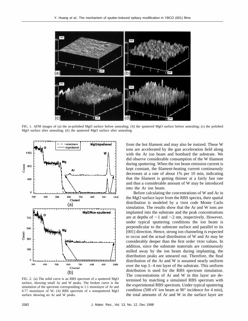
The actual surface morphology changes causedion sputtering were examined by AFM and cross-sectTEM. The AFM results are shown in Fig. 1. The imagin Fig. 1(a) shows the surface of the as-polished Mgwhich is very flat with the height fluctuation on thsurface smaller than 1 nm. After ion sputtering tsubstrate becomes much rougher with height fluctuaas large as 5–10 nm [Fig. 1(b)]. This difference betwenonsputtered and sputtered surfaces, however, is lardiminished by a 30 min annealing in an oxygen plasat ,670 ±C that is routinely performed before YBCOfilm growth. After the annealing both nonsputtered asputtered substrates have similar surface morphologrelatively larger bumps 0.1–0.3mm in size [Figs. 1(c)and 1(d)]. The only difference is the bump height. Taverage bump height is about 6 nm on the nonsputtesubstrates and about twice this value on the sputtesubstrates.
Since the lateral resolution of AFM is relativelpoor, the cross-sectional TEM is used to examinefiner detail in the surface morphology change. No snificant difference regarding atomic-scale featuresbe seen between these two substrates, except thalong-range (.100 nm) height fluctuation is larger othe sputtered surfaces than on the nonsputtered surfSince the initial growth of the YBCO films is an atomicscale process, the surface morphology features waffect the film orientation must be on the atomic scaTherefore, the fact that TEM observation showssignificant difference in the atomic-scale surface mphology reinforces the conclusion reached above thatsurface morphology change caused by ion sputterinnot an important factor in SIEM.
B. The surface composition change induced byion sputtering
The composition change of the substrate surflayer during ion sputtering was examined by RBS. Fure 2(a) shows a typical RBS spectrum of the Mgsubstrate sputtered with an ion gun that employs aW filament to ionize the Ar ion. In addition to the higMg and O edges, there are two small extra peaks inspectrum that correspond to Ar and W. It is believed tthe Ar and W are introduced into the substrate by theirradiation since RBS of the nonsputtered MgO doesshow these two elements; see Fig. 2(b). The source oW must be the hot W filament of the ion gun. When tion gun is on, electrons are emitted by the hot filameaccelerated by the “discharge” electric field and forcto move in spiral orbits by a magnetic field. Ar atomsthe discharge chamber are ionized by these electronsthe same time some W atoms are evaporated or sputt
3, No. 12, Dec 1998 3381
Y. Huang et al.: The mechanism of sputter-induced epitaxy modification in YBCO (001) films
olished
FIG. 1. AFM images of (a) the as-polished MgO surface before annealing; (b) the sputtered MgO surface before annealing; (c) the pMgO surface after annealing; (d) the sputtered MgO surface after annealing.gt
g
Wngent
t isslyingteed
inial
reons
isits
ede
slyenal
mn.e-ithng
re
(a)
(b)FIG. 2. (a) The solid curve is an RBS spectrum of a sputtered Msurface, showing small Ar and W peaks. The broken curve issimulation of the spectrum corresponding to 1.1 monolayer of Ar a0.77 monolayer of W; (b) RBS spectrum of a nonsputtered Msurface showing no Ar and W peaks.
3382 J. Mater. Res., Vol. 1
OhendO
from the hot filament and may also be ionized. Theseions are accelerated by the gun acceleration field alowith the Ar ion beam and bombard the substrate. Wdid observe considerable consumption of the W filameduring sputtering. When the ion beam emission currenkept constant, the filament-heating current continuoudecreases at a rate of about 1% per 10 min, indicatthat the filament is getting thinner at a fairly fast raand thus a considerable amount of W may be introducinto the Ar ion beam.
Before calculating the concentrations of W and Arthe MgO surface layer from the RBS spectra, their spatdistribution is modeled by aTRIM code Monte Carlosimulation. The results show that the Ar and W ions aimplanted into the substrate and the peak concentratiare at depths of,1 and,2 nm, respectively. However,under typical sputtering conditions the ion beamperpendicular to the substrate surface and parallel to[001] direction. Hence, strong ion channeling is expectto occur and the actual distribution of W and Ar may bconsiderably deeper than the first orderTRIM values. Inaddition, since the substrate materials are continuoumilled away by the ion beam during implanting, thdistribution peaks are smeared out. Therefore, the fidistribution of the Ar and W is assumed nearly uniformover the top 3–4 nm layer of the substrate. This unifordistribution is used for the RBS spectrum simulatioThe concentrations of Ar and W in this layer are dtermined by matching a simulated RBS spectrum wthe experimental RBS spectrum. Under typical sputtericondition (500 eV ion beam at 90± incidence for 4 min),the total amounts of Ar and W in the surface layer a
3, No. 12, Dec 1998

Y. Huang et al.: The mechanism of sputter-induced epitaxy modification in YBCO (001) films
l
tuah
tt
a
e
eoonn
e
ehitd
ete.-
end
re
g,e
her
ion
ts-oas)].
oty
On
ace
rcees.n
nund
s
dndeseay
ial
approximately 1.1 and 0.77 monolayers, respectiveConsidering the Ar ion beam current of 1 mAycm2,less than 0.2% of the Ar ions stay in the substrate afsputtering. The emission rate of W is not known, bit must be much smaller than for Ar. Since the finW concentration is close to the Ar concentration, timplantation ratio of W ions must be much higher thathat of Ar ions. This phenomenon can be attributedseveral effects, including the larger implantation depof the W ions and the smaller mobility of W ions inthe substrate surface layer due to their larger massstronger interaction with substrate atoms.
The difference between the mobility of Ar and Wions in the substrate surface layer can also be sfrom the change of their concentration with sputterintime. Both Ar and W concentration in the surface layincrease with sputtering time, but the Ar concentratisaturates in less than 1 min while the W concentraticontinues to increase up to 10 min of the sputteritime [Fig. 3(a)]. The early saturation of Ar ions cabe understood by considering the milling effect of thsubsequent Ar ion beam. During the sputtering proc
(a)
(b)FIG. 3. (a) Variation of Ar and W concentration with sputtering timas determined by RBS. The Ar concentration saturates in less t30 s of sputtering. (b) Ar and W concentration both increase wion incident angle. The ratio of the 0± oriented phase on the sputteresurface shows the same trend as the W concentration.
J. Mater. Res., Vol. 13
y.
ertlenoh
nd
engrnng
ess
anh
previously implanted ions are partly removed from thsubstrate while new ions are implanted in the substraAfter an initial transition period a steady-state concentration will be reached. The higher the removal ratof the implanted ions, the faster the final concentratiois reached. The Ar ions are more loosely bound animplanted to a shallower depth than the W ions, therefothe probability for the Ar ions being removed from theMgO surface layer by the subsequent ion sputterinis much greater than that for the W ions. In additionsince Ar is an inert gas, it may be stable in the surfacregion only in the form of subsurface clusters from whicAr may eventually escape from the substrate into thvacuum. Both effects cause higher removal rates of Aby the sputtering; therefore the steady-state concentratof Ar is reached much faster than that of W.
The early saturation of Ar concentration suggesthat Ar implantation may not be important to the occurrence of SIEM. No SIEM occurs for a 1 min exposure tthe ion beam (see Table I), and the Ar concentration halready become saturated at this stage [see Fig. 3(aThe W concentration, on the other hand, does nsaturate until after SIEM is observed and therefore mahave an important effect on the change of the YBCorientation. Shown in Fig. 3(b) are the W concentratioand the fraction of the 0± oriented phase; both increasewith increasing ion incident angle. This again suggestsconnection between W implantation and the occurrenof SIEM. To further explore this connection, YBCOfilms were grown on MgO substrates sputtered by an Aion gun that uses an rf field to generate the Ar ions; henno W ions are generated or implanted into the substratAll other conditions were the same as with the tungstefilament ion gun. In the resultant films the fraction of the0± phase is greatly diminished from that observed whesubstrates are sputtered with a tungsten filament ion gand only slightly larger than that of the nonsputterecase, indicating that W-free Ar ion sputtering has littleeffect on the occurrence of SIEM (see Fig. 4). Thus, Wimplantation appears essential to SIEM.
In the POMBE procedure the substrate is alwaytreated with an oxygen plasma at,670 ±C for 30 minbefore the growth of YBCO film. To determine if theimplanted ions are lost in this treatment, sputteresubstrates were examined by RBS both before aafter the predeposition treatment. The result indicatthat most of the Ar and W remain in the substratafter the plasma treatment and are not sputtered awby the oxygen plasma.
C. Effects of the initial film growth conditions
The YBCO film growth conditions affect the YBCOfilm orientation on MgO. The POMBE deposition systemdelivers the metal precursors to the substrate in a ser
, No. 12, Dec 1998 3383

Y. Huang et al.: The mechanism of sputter-induced epitaxy modification in YBCO (001) films
ethtr
tAeo
esnis
fiisn
nt
uh
c
ia
m-a
t
r
-
as-l
t
e
r
e
nsal
n
a’s
s
eerre
-
ra
shee-
isehg
FIG. 4. The ratio of 0± oriented YBCO films on the substrate surfacchanges with the length of the initial Ba pulse in the POMBE growThe three curves show the change under three different substreatment conditions.
sequence of discrete pulses. The type and amounmetal precursor in each pulse can be controlled.important factor in the control of film orientation is thtype and amount of precursor in the initial film layer. Tobtain SIEM, a Ba layer of a certain thickness needsbe deposited first. In the POMBE system this is realizby controlling the length of the first Ba precursor pulunder a calibrated constant flow rate. The dependeof the film orientation on the first Ba pulse lengthillustrated in Fig. 4, which plots the ratio of 0± orientedareas over the total substrate surface versus theBa pulse time. When this ratio is 0, the whole filmoriented at 45±. The three curves in the figure correspoto the MgO (001) substrates nonsputtered, sputtereda W-free Ar ion gun, and sputtered by an Ar ion guwith a W filament, respectively. The incorporation raof Ba atoms into the deposited film is about 0.133
1015 Baycm2 s.For all three types of substrates the YBCO film
grow entirely in 0± orientation when the initial Ba pulseis longer than 9 s. This means that if we deposit a sficient amount of Ba onto the MgO surface before tYBCO growth, we always get 0± oriented YBCO filmsregardless of substrate treatment. This phenomenonbe called “Ba-induced 0± growth.”36 When the initial Bapulse is short, however, the film orientation can be dferent. For the two W-free surfaces there is a criticBa pulse length below which the resultant YBCO filswitches to 45± orientation. The switching of the orientation is quite abrupt. On the nonsputtered substrfor example, the YBCO film changes from 100% of 0±
orientation to 100% of 45± orientation when the initialBa pulse decreases from 8.6 to 5.7 s. This givescritical Ba pulse length for a nonsputtered substrateabout 5.7 s, which corresponds to a critical Ba coveraof 0.74 3 1015 Baycm2 or 1.1 monolayers of BaO. Fo
3384 J. Mater. Res., Vol. 13
.ate
ofn
tod
ece
rst
dby
e
s
f-e
an
f-l
te,
heasge
the substrate sputtered by an ion gun with a W filament the films are always grown in 0± orientation. Evenwhen the deposition was started with a Y layer (i.e.,Ba pulse time of 0 s), more than 99% of the films growwith 0± orientation. In this case we can say that the critical Ba pulse length is zero. The change of the criticaBa pulse length by the sputtering forms a time windowfrom 1 s to 5.7 s. Within this window one can grow the0± oriented phase on regions sputtered with a W filamenion gun and the 45± oriented phase on the nonsputteredregions simultaneously. This makes the fabrication of th45± tilt boundary with the SIEM method possible.
The phenomenon of “Ba-induced 0± growth” hasbeen explained in terms of the initial growth behavioof BaO on the MgO (001) surface.36 In a study of BaOgrowth on MgO (001), Cotteret al.35 found that for Bacoverage less than a critical value (2–3 monolayers), thBa atoms are substitutionally incorporated into the MgOlattice and the surface structure of the substrate remaiunchanged. For Ba coverage greater than the criticvalue, an epitaxial BaO overlayer was formed. Thec-axis of this overlayer is aligned with that of MgO andthe in-plane orientation relation is [110]BaOyy[100]MgO.The above observation was justified by a calculatioof the heat of segregation.40 Their calculations showthat the formation of a BaO overlayer is energeticallyfavorable over substitutional incorporation as the Bcoverage exceeded a critical coverage. Using Cotterresults, Buccholzet al.13,36 proposed a model for the Ba-induced 0± growth. They believed that Cotter’s criticalBa coverage for BaO overlayer to form correspondto the critical initial Ba pulse length in the POMBEgrowth. Below this critical Ba coverage the surfaceretains the MgO (001) structure and the YBCO filmsare grown in the 45± orientation. When more Ba isdeposited onto the surface, the concentration of thsubstitutional Ba atoms in the substrate surface laywill finally reach a saturation point and a BaO overlayestarts to form over the Ba saturated MgO layer. Thsubsequent YBCO films grow on the BaO overlayer withthe orientation relation [100]YBCOyy[110]BaO, giving theoverall 0± orientation relation between YBCO films andthe MgO substrate.
To explore the above model, TEM is used to examine a 0± oriented YBCOyMgO interface formed ona nonsputtered MgO substrate by depositing an extamount of Ba in the initial stage of film growth. Figure 5is a cross-section HREM image of this interface. Thiimage shows that the top layer of the substrate has tsame lattice fringes as the bulk MgO, except for sommodification in contrast. It appears that this layer corresponds to the Ba saturated MgO top layer. Above thlayer we expect to see a BaO overlayer. However, wdid not see this overlayer in the image, even if the lengtof the first Ba pulse was as long as 30 s, correspondin
, No. 12, Dec 1998

Y. Huang et al.: The mechanism of sputter-induced epitaxy modification in YBCO (001) films
g
no
rsnh
r
Bn
at
d
d
l
u
ht
nn
re
d
s.-
ef)fs
ale
n
r
FIG. 5. Cross-sectional HREM image of the 0± oriented YBCOyMgOinterface induced by extra amount of Ba deposition in the initial staof the film growth.
to more than 6 monolayers of BaO. The elemental liprofile across the interface obtained by high resolutiEDX also shows no extra Ba-rich layer at the interface.possible explanation for the absence of the BaO layethat it disappears in the subsequent film growth proceSince Ba is one of the constituents of YBCO, diffusiomay occur under the high temperature during the syntsis so that the extra Ba is incorporated into the YBCfilm. The initial existence of this BaO layer, howevemust cause the 0± orientation in the YBCO film.
Since extra initial Ba deposition leads to 0± growth,one could propose that the ion sputtering might increaBa production on the sputtered areas and cause a “induced 0± growth”. A possible mechanism is that aenhanced Ba deposition could result from an increain the adsorption and/or decomposition rate of the Bprecursor by sputter-induced defects, such as stepsledges that could increase the reaction rate, or by creaa surface chemical environment which is more favorabfor the decomposition. If this speculation were correcthe mechanism of SIEM would be a form of “Ba-induce0± growth”.
In order to find out whether or not this is indeethe case, a critical experiment was performed. In thexperiment only the initial Ba layer was simultaneousdeposited onto sputtered and nonsputtered substraand the resultant Ba concentrations on these two sstrates were measured by RBS. No significant differenbetween the two substrates was found. This indicates tion sputtering does not increase Ba deposition onsubstrate surface. Therefore, the mechanism of SIEMnot a form of “Ba-induced 0± growth”.
D. Microstructure of the YBCO yyyMgO interfaces
A possible mechanism of SIEM is that the Ar iosputtering and W implantation may cause some ki
J. Mater. Res., Vol. 13
e
enAiss.
e-O,
sea-
seand
inglet,
isytes,b-
ceat
heis
d
of structural changes in the surface MgO lattice and/oform a buffer layer at the surface that relieves the larglattice mismatch associated with the 0± growth. In orderto characterize these structural changes, HREM is useto examine the 45± tilt grain boundaries fabricated withthe SIEM method and the YBCOyMgO interfaces in thenonsputtered and sputtered regions.
HREM imaging shows a remarkable change in theinterface structure after ion sputtering. Figure 6 is across-sectional TEM image of the root part (near thefilm/substrate interface) of a 45± tilt grain boundaryformed between the sputtered and nonsputtered regionThe detailed structure of this boundary has been discussed elsewhere.16 What we want to show here is thedifference in the YBCOyMgO interfaces on the twosides of the boundary. In the nonsputtered region thinterface is sharp, but in the sputtered region a layer odifferent contrast is formed at the interface. Figures 7(aand 7(b) represent closer views of these two types ointerfaces. The interface in the nonsputtered sample[Fig. 7(a)] is sharp and clean. The YBCO films growdirectly on the MgO surface. There are no reactionproducts or intermediate layer at the interface. AlthoughBa is deposited as the initial layer of the YBCO growth,no extra layer is observed at this interface. It is believedthat the initial Ba layer is incorporated into the YBCOlayers in the subsequent growth process. The periodicfeatures at the interface indicated by arrows suggest thformation of interfacial dislocations that match everyfour MgO [200] planes with three YBCO [110] planes.The interface in the sputtered samples [Fig. 7(b)], onthe other hand, is not sharp. It is characterized by aintermediate layer 3–6 nm thick. This layer displaysdifferent lattice fringes compared to other parts of thesample, indicating that it has a structure different fromeither YBCO or MgO.
In addition to the difference in lattice structure,the elemental composition and spatial distribution nea
FIG. 6. HREM image of the root part of a 45± grain boundary formedby the SIEM method. Notice that the YBCOyMgO interfaces in thetwo sides of the boundary are different.
, No. 12, Dec 1998 3385

Y. Huang et al.: The mechanism of sputter-induced epitaxy modification in YBCO (001) films
r
i
a
i
r
d
.e
e
is
f
d
.le
aeseOe
nedhe
FIG. 7. YBCOyMgO interfaces in (a) nonsputtered MgO region an(b) sputtered MgO region. Note that the periodical contrast featuindicated by arrows in (a) are formed by interface dislocations and tthere is an intermediate layer formed between YBCO and MgO in (
the interface regions are also different in the nonsptered and sputtered samples. This can be seen fthe elemental line profiles shown in Fig. 8, which aobtained by high spatial resolution EDX line scan. Aboth interfaces the Mg concentration drops down slowas the probe is moved from the MgO side to the YBCside, indicating some degree of Mg diffusion into YBCOThe concentration profile of Y, Ba, and Cu, howeveis different between the nonsputtered and the sputteinterfaces. In the nonsputtered sample the concentratof the three elements change abruptly as the procrosses the interface, indicating a sharp YBCO edIn other words, there is no diffusion of Y, Cu, or Binto the MgO. In the sputtered sample, however, theconcentration increases a few nanometers ahead oand Cu concentration while the probe is moved froMgO to YBCO, indicating a Ba-rich layer a few nmthick at the interface. It is believed that this Ba-riclayer corresponds to the intermediate layer observin the HREM images. The major composition of thlayer is a mixture of barium, magnesium, and oxygewith relatively small amount of yttrium and coppeThe molecular formula of this layer could be writteas BaxMg12xO. It is evident that the formation of thislayer is caused by Ba diffusion from the deposited layinto the substrate. The first layer Ba deposition w
3386 J. Mater. Res., Vol. 1
dreshatb).
ut-om
retlyO.r,redonsbe
ge.
Baf Ym
hedsn,.n
erill
FIG. 8. Elemental line profile by high resolution EDX across theYBCOyMgO interfaces in (a) nonsputtered region and (b) sputtereregion.
definitely help in the formation of this intermediate layerThis is consistent with the fact that some length of thfirst Ba pulse in the POMBE growth is essential forthe orientation change to occur. Also observed in thnarrow (a few nm wide) YBCOyMgO interface regionof the sputtered sample is a small amount of W. No Wis observed at the nonsputtered interface. This factconsistent with the RBS result mentioned in Sec. III. Band suggests the critical effect of W in the formation othe Ba-rich intermediate layer.
E. The mechanism of sputter-inducedepitaxy modification
In the above sections we have found that the Wion implantation associated with the ion sputtering anthe first Ba layer in the YBCO film growth are thetwo most important factors for the occurrence of SIEMWe also observed a large difference in the atomic-scastructure of the YBCOyMgO interface between sputteredand nonsputtered regions. In the sputtered regionBa-rich intermediate layer is observed, which has thsame thickness as the W implanted layer. From theexperimental results, the process occurring on the Mgsurfaces in the early stage of YBCO growth and thmechanism by which the different growth orientationson the sputtered and nonsputtered substrates are obtaican be described as below. On the nonsputtered MgO t
3, No. 12, Dec 1998

Y. Huang et al.: The mechanism of sputter-induced epitaxy modification in YBCO (001) films
mee
o
e
h
sa
a
oo
u
sM
Ao
a
small amount of the initial Ba deposition does not changthe surface structure of the substrate and the YBCO filgrows “normally” on the substrate with no intermediatlayer formed. Here the word “normally” means that thfilm grows exclusively in the 45± orientation becausethis orientation results in a smaller lattice mismatch tthe substrate. On the sputtered surface, however, theimplantation, and to some extent the Ar ion sputteringintroduce some kind of structural and chemical changin the surface layer of the substrate, which lead to Bdiffusion into the MgO surface layer. This diffusionforms on the substrate surface a layer of BaxMg12xOthat functions as a buffer for the subsequent film growtThe initial deposition of Ba also helps in the formationof this buffer layer. The presence of the buffer layeon the MgO surface avoids the large lattice mismatcbetween MgO and 0± oriented YBCO film and makesthe 0± oriented growth energetically favorable.
At this moment, it is not clear what structural andchemical changes are induced by the W ion implantatioduring sputtering. One possible change is that W ioncreate a large amount of vacancies in MgO on their paof implantation due to their large mass. The existencof these vacancies enhances the diffusion of Ba atomlater in the film growth process. The consistency betweethe thickness of the diffusion layer and the depth of thW implantation (both of them are a few nm) seemto support this assumption. The reason why Ba hsignificantly stronger diffusion than Y and Cu may bethat Ba has the same valance structure as Mg in contrto Y and Cu. Another possible effect of the W ionimplantation is the change in the electronic structurethe MgO surface layer since W has a different numbervalance electrons compared to Mg. The details on thestructural and chemical changes and the exact structand composition of the intermediate layer induced by thion sputtering are the objects of further investigations.
IV. CONCLUSION
The mechanism of the sputter-induced epitaxy modfication (SIEM) occurring in YBCO films grown onMgO (001) surfaces has been investigated throughseries of film growth and characterization experimentThe effects of several factors on the occurrence of SIEare studied. First, the surface morphology change causby ion sputtering is found not to be a major factorAlthough the sputtered surface is rougher on a largscale, no significant difference regarding atomic-scafeatures on the sputtered and nonsputtered surfacesobserved. Second, the Ar implantation into the substrais also excluded as a major factor because theconcentration on the sputtered surface saturates befany SIEM occurs. Third, W ion implantation is identifiedas one of the most important factors that induce SIEM
J. Mater. Res., Vol. 13
e
W,s
a
.
rh
nsthes
ne
s
st
ff
seree
i-
a.
ed.ele
isterre
.
This is confirmed by comparing the film growth resultsusing ion guns with and without W filament. Finally, theinitial Ba deposition is found to be essential to controlthe film growth orientation.
By analyzing the experimental results regardingthese relevant factors and by studying the microstructureand elemental distribution of the resultant YBCOyMgOinterfaces, the mechanism of SIEM is elucidated asfollows. On the nonsputtered MgO (001) surface YBCOgrows in the 45± orientation because of the smaller latticemismatch in this orientation. On the sputtered surface theW implantation associated with the sputtering inducessome structural and chemical changes that cause Bdiffusion into the damaged MgO surface layer and forma BaxMg12xO buffer layer on top of the substrate surface.The formation of this buffer layer is also helped by theinitial Ba deposition in the POMBE growth. This bufferlayer relieves the large lattice mismatch between MgOand the 0± oriented YBCO layer and thus makes the 0±
growth possible on the sputtered surfaces.
ACKNOWLEDGMENTS
The authors are grateful to V. Dravid, W. A. Chiou,and Y. Y. Wang for help in the microanalysis, to R. Csen-csits, H. Zhang, and W. Sinkoer for their help in theHREM experiments, and to L. J. Thompson and F. R.Ding for help withTRIM and RBS simulation. This workis supported by the National Science Foundation, underContract No. DMR 91-20000 (YH, BVV) and the UnitedStates Department of Energy under Contract No. W-31-109-ENG-38 (KLM).
REFERENCES
1. K. P. Daly, W. D. Dozier, J. F. Burch, S. B. Coons, R. Hu, C. E.Platt, and R. W. Simon, Appl. Phys. Lett.58, 543 (1991).
2. C. L. Jia, B. Kabius, K. Urban, K. Herrmann, J. Schubert,W. Zander, and A. I. Braginski, Physica C196, 211 (1992).
3. D. Dimos, P. Chaudhari, and J. Mannhart, Phys. Rev. B41, 4038(1990).
4. D. Dimos, P. Chaudhari, J. Mannhart, and F. K. LeGoues, Phys.Rev. Lett. 61, 219 (1988).
5. H. B. Lu, T. W. Huang, J. J. Wang, J. Lin, S. L. Tu, S. J. Yang,and S. E. Hsu, IEEE Trans. Appl. Supercond.3, 2325 (1993).
6. K. Char, M. S. Colclough, S. M. Garrison, N. Newman, andG. Zaharchuk, Appl. Phys. Lett.59, 733 (1991).
7. R. P. J. Ijsselsteijn, J. W. M. Hilgenkamp, M. Eisenberg, C. Vittoz,J. Flokstra, and H. Rogalla, J. Allo. Comp.195, 231 (1993).
8. N. G. Chew, S. W. Goodyear, R. G. Humphreys, J. S. Satchell,J. A. Edwards, and M. N. Keene, Appl. Phys. Lett.60, 1516(1992).
9. N. G. Chew (1992), private communication.10. B. V. Vuchic, K. L. Merkle, K. A. Dean, D. B. Buchholz, R. P. H.
Chang, and L. D. Marks, J. Appl. Phys.77, 2591 (1995).11. B. V. Vuchic, K. L. Merkle, J. W. Funkhouser, D. B. Buchholz,
K. A. Dean, R. P. H. Chang, and L. D. Marks, IEEE Trans. Appl.Supercond. (1995).
, No. 12, Dec 1998 3387

Y. Huang et al.: The mechanism of sputter-induced epitaxy modification in YBCO (001) films
c
Hr
e
l.
y
,
.
r
t
au
Y.
d
.
,
n,
rf.
.,
,in
c.
B.
.
12. B. V. Vuchic, K. L. Merkle, P. M. Baldo, K. A. Dean, D. B.Buchholz, R. P. H. Chang, H. Zhang, and L. D. Marks, PhysiC 270, 75 (1996).
13. D. B. Buchholz, J. S. Lei, S. Mahajan, P. R. Markworth, R. P.Chang, B. Hinds, T. J. Marks, J. L. Schindler, C. R. KannewuY. Huang, and K. L. Merkle, Appl. Phys. Lett.68, 3037 (1996).
14. M. Aindow, T. T. Cheng, and D. D. Norris, Philos. Mag. Lett.74,267 (1996).
15. A. Gervais and D. Keller, Physica C246, 29 (1995).16. Y. Huang, B. V. Vuchic, D. B. Buccholz, K. L. Merkle, and
R. P. H. Chang, Proc. 54th Annu. meeting, MSA, edited by G. WBailey (San Francisco Press, San Francisco, CA, 1996), p. 37
17. D. M. Hwang, T. S. Ravi, R. Ramesh, S-W. Chan, and C. Y. ChAppl. Phys. Lett.57, 1690 (1990).
18. M. Kamei, Y. Aoki, S. Ogota, T. Usui, and T. Morishita, J. AppPhys.74, 436 (1993).
19. S-T. Lee, S. Chen, L. S. Hung, and G. Braunstein, Appl. PhLett. 55, 286 (1989).
20. C. LePaven-Thivet, M. Guilloux-Viry, J. Padiou, A. PerrinM. Sergent, L. A. deVaulchier, and N. Bontempts, Physica C244,231 (1995).
21. Q. Li, O. Meyer, X. X. Xi, J. Geerk, and G. Linker, Appl. PhysLett. 55, 310 (1989).
22. S. McKernan, M. G. Narton, and C. B. Carter, J. Mater. Res.7,1052 (1992).
23. M. G. Norton, L. A. Tietz, S. R. Summerfelt, and C. B. CarteAppl. Phys. Lett.55, 2348 (1989).
24. M. G. Norton and C. B. Carter, J. Cryst. Growth110, 641 (1991).25. M. G. Norton and C. B. Carter, Scanning Microsc.6, 385 (1992).26. S. J. Pennycook, M. F. Chisholm, D. E. Jesson, R. Feens
S. Zhu, X. Y. Zheng, and D. J. Lowndes, Physica C202, 1 (1992).27. R. Ramish, D. Hwang, T. S. Ravi, A. Inam, J. G. Barner, L. Naz
S. W. Chan, C. Y. Chen, B. Dutta, T. Benkatesan, and X. D. WAppl. Phys. Lett.56, 2243 (1990).
3388 J. Mater. Res., Vol. 13
a
.f,
.2.n,
s.
,
ra,
r,,
28. T. S. Ravi, D. M. Hwang, R. Ramesh, S. W. Chan, L. Nazar, C.Chen, A. Inam, and T. Venkatesan, Phys. Rev. B42, 10 141(1990).
29. N. Savvides and A. Katsaros, Physica C226, 23 (1994).30. D. H. Shin, J. Silcox, S. E. Rssek, D. K. Lathrop, B. Moeckly, an
R. A. Buhrman, Appl. Phys. Lett.57, 508 (1990).31. S. K. Streiffer, B. M. Lairson, C. B. Eom, B. M. Clemens, and J. C
Bravman, Phys. Rev. B43, 13007 (1991).32. H. Suzuki, Y. Fujiwara, Y. Hirotsu, T. Yamashita, and T. Oikawa
Jpn. J. Appl. Phys.32, 1601 (1993).33. M. Suzuki and H. Sakurai, IEEE Trans. Appl. Supercond.5, 1233
(1995).34. C. Traeholt, J. G. Wen, V. Svetchnikov, and H. W. Zandberge
Physica C230, 297 (1994).35. M. Cotter, S. Campbell, R. G. Edgell, and W. C. Mackpodt, Su
Sci. 197, 208 (1988).36. D. B. Buchholz, J. S. Lei, S. Mahajan, P. R. Markworth, R. P. H
Chang, B. Hinds, T. J. Marks, Y. Huang, and K. L. MerkleJ. Allo. Comp.251, 278 (1997).
37. Y. Huang, B. V. Vuchic, P. Baldo, K. L. Merkle, D. B. BuchholzS. Mahajan, J. S. Lei, P. R. Markworth, and R. P. H. Chang,Interfacial Engineering for Optimized Properties,edited by C. L.Briant, C. B. Carter, and E. L. Hall (Mater. Res. Soc. Symp. Pro458, Pittsburgh, PA, 1997), p. 497.
38. S. J. Duray, D. B. Buchholz, S. N. Song, D. S. Richardson, J.Ketterson, T. J. Marks, and R. P. H. Chang, Appl. Phys. Lett.59,1503 (1991).
39. Y. Huang and K. L. Merkle, inSpecimen Preparation for Trans-mission Electron Microscopy of Materials IV,edited by R. M.Anderson and S. D. Walck (Mater. Res. Soc. Symp. Proc.480,Pittsburgh, PA, 1997), p. 235.
40. M. Cotter, S. Campbell, L. L. Cao, R. G. Egdell, and W. CMackrodt, Surf. Sci.208, 267 (1989).
, No. 12, Dec 1998