Student Guide Thwarting the Enemy: Providing CITA ... - CDSE
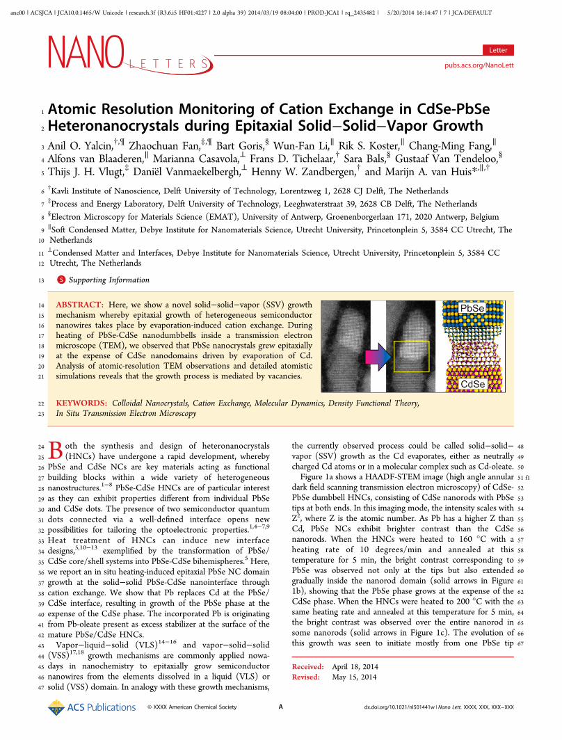
1 Atomic Resolution Monitoring of Cation Exchange in CdSe-PbSe2 Heteronanocrystals during Epitaxial Solid−Solid−Vapor Growth3 Anil O. Yalcin,†,¶ Zhaochuan Fan,‡,¶ Bart Goris,§ Wun-Fan Li,∥ Rik S. Koster,∥ Chang-Ming Fang,∥
4 Alfons van Blaaderen,∥ Marianna Casavola,⊥ Frans D. Tichelaar,† Sara Bals,§ Gustaaf Van Tendeloo,§
5 Thijs J. H. Vlugt,‡ Daniel Vanmaekelbergh,⊥ Henny W. Zandbergen,† and Marijn A. van Huis*,∥,†
6†Kavli Institute of Nanoscience, Delft University of Technology, Lorentzweg 1, 2628 CJ Delft, The Netherlands
7‡Process and Energy Laboratory, Delft University of Technology, Leeghwaterstraat 39, 2628 CB Delft, The Netherlands
8§Electron Microscopy for Materials Science (EMAT), University of Antwerp, Groenenborgerlaan 171, 2020 Antwerp, Belgium
9∥Soft Condensed Matter, Debye Institute for Nanomaterials Science, Utrecht University, Princetonplein 5, 3584 CC Utrecht, The
10 Netherlands
11⊥Condensed Matter and Interfaces, Debye Institute for Nanomaterials Science, Utrecht University, Princetonplein 5, 3584 CC
12 Utrecht, The Netherlands
13 *S Supporting Information
14 ABSTRACT: Here, we show a novel solid−solid−vapor (SSV) growth15 mechanism whereby epitaxial growth of heterogeneous semiconductor16 nanowires takes place by evaporation-induced cation exchange. During17 heating of PbSe-CdSe nanodumbbells inside a transmission electron18 microscope (TEM), we observed that PbSe nanocrystals grew epitaxially19 at the expense of CdSe nanodomains driven by evaporation of Cd.20 Analysis of atomic-resolution TEM observations and detailed atomistic21 simulations reveals that the growth process is mediated by vacancies.
22 KEYWORDS: Colloidal Nanocrystals, Cation Exchange, Molecular Dynamics, Density Functional Theory,23 In Situ Transmission Electron Microscopy
24 Both the synthesis and design of heteronanocrystals25 (HNCs) have undergone a rapid development, whereby26 PbSe and CdSe NCs are key materials acting as functional27 building blocks within a wide variety of heterogeneous28 nanostructures.1−8 PbSe-CdSe HNCs are of particular interest29 as they can exhibit properties different from individual PbSe30 and CdSe dots. The presence of two semiconductor quantum31 dots connected via a well-defined interface opens new32 possibilities for tailoring the optoelectronic properties.1,4−7,9
33 Heat treatment of HNCs can induce new interface34 designs,5,10−13 exemplified by the transformation of PbSe/35 CdSe core/shell systems into PbSe-CdSe bihemispheres.5 Here,36 we report an in situ heating-induced epitaxial PbSe NC domain37 growth at the solid−solid PbSe-CdSe nanointerface through38 cation exchange. We show that Pb replaces Cd at the PbSe/39 CdSe interface, resulting in growth of the PbSe phase at the40 expense of the CdSe phase. The incorporated Pb is originating41 from Pb-oleate present as excess stabilizer at the surface of the42 mature PbSe/CdSe HNCs.43 Vapor−liquid−solid (VLS)14−16 and vapor−solid−solid44 (VSS)17,18 growth mechanisms are commonly applied nowa-45 days in nanochemistry to epitaxially grow semiconductor46 nanowires from the elements dissolved in a liquid (VLS) or47 solid (VSS) domain. In analogy with these growth mechanisms,
48the currently observed process could be called solid−solid−49vapor (SSV) growth as the Cd evaporates, either as neutrally50charged Cd atoms or in a molecular complex such as Cd-oleate.51 f1Figure 1a shows a HAADF-STEM image (high angle annular52dark field scanning transmission electron microscopy) of CdSe-53PbSe dumbbell HNCs, consisting of CdSe nanorods with PbSe54tips at both ends. In this imaging mode, the intensity scales with55Z2, where Z is the atomic number. As Pb has a higher Z than56Cd, PbSe NCs exhibit brighter contrast than the CdSe57nanorods. When the HNCs were heated to 160 °C with a58heating rate of 10 degrees/min and annealed at this59temperature for 5 min, the bright contrast corresponding to60PbSe was observed not only at the tips but also extended61gradually inside the nanorod domain (solid arrows in Figure621b), showing that the PbSe phase grows at the expense of the63CdSe phase. When the HNCs were heated to 200 °C with the64same heating rate and annealed at this temperature for 5 min,65the bright contrast was observed over the entire nanorod in66some nanorods (solid arrows in Figure 1c). The evolution of67this growth was seen to initiate mostly from one PbSe tip
Received: April 18, 2014Revised: May 15, 2014
Letter
pubs.acs.org/NanoLett
© XXXX American Chemical Society A dx.doi.org/10.1021/nl501441w | Nano Lett. XXXX, XXX, XXX−XXX
anc00 | ACSJCA | JCA10.0.1465/W Unicode | research.3f (R3.6.i5 HF01:4227 | 2.0 alpha 39) 2014/03/19 08:04:00 | PROD-JCA1 | rq_2435482 | 5/20/2014 16:14:47 | 7 | JCA-DEFAULT
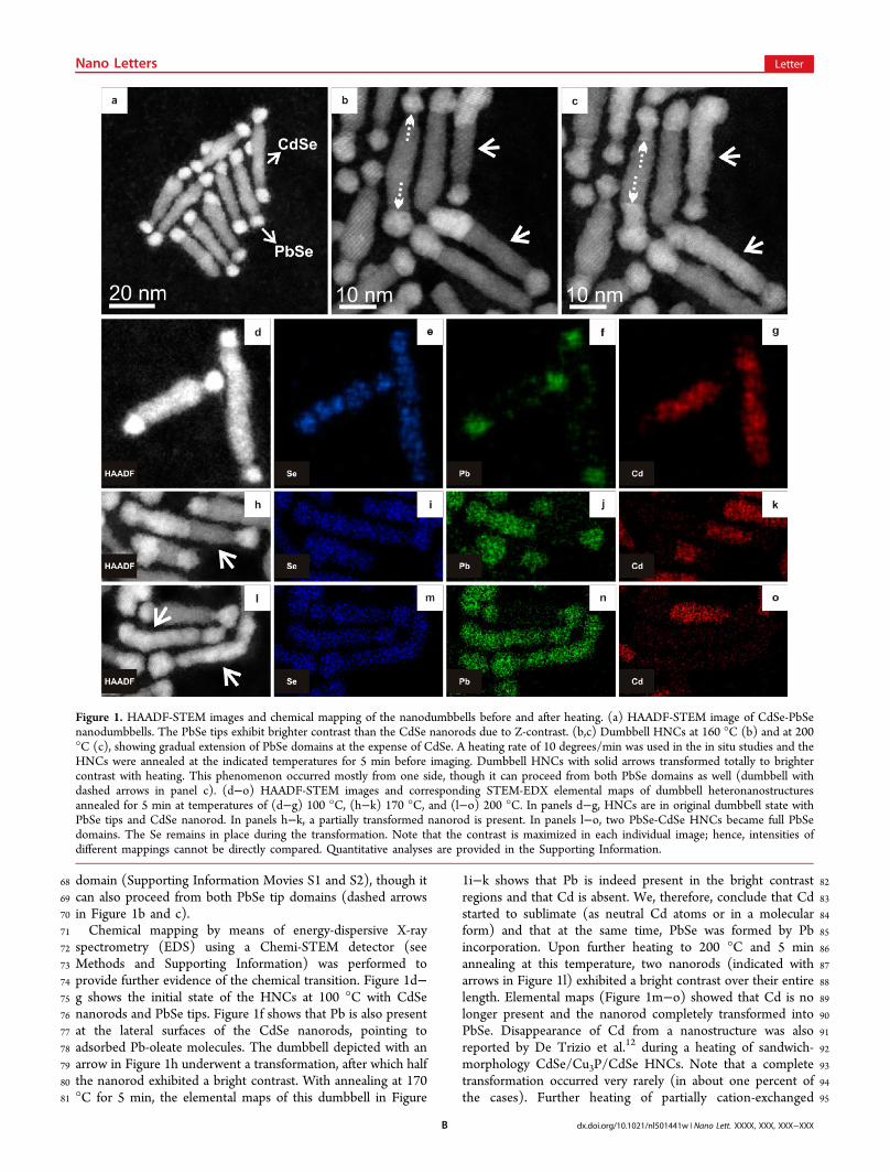
68 domain (Supporting Information Movies S1 and S2), though it69 can also proceed from both PbSe tip domains (dashed arrows70 in Figure 1b and c).71 Chemical mapping by means of energy-dispersive X-ray72 spectrometry (EDS) using a Chemi-STEM detector (see73 Methods and Supporting Information) was performed to74 provide further evidence of the chemical transition. Figure 1d−75 g shows the initial state of the HNCs at 100 °C with CdSe76 nanorods and PbSe tips. Figure 1f shows that Pb is also present77 at the lateral surfaces of the CdSe nanorods, pointing to78 adsorbed Pb-oleate molecules. The dumbbell depicted with an79 arrow in Figure 1h underwent a transformation, after which half80 the nanorod exhibited a bright contrast. With annealing at 17081 °C for 5 min, the elemental maps of this dumbbell in Figure
821i−k shows that Pb is indeed present in the bright contrast83regions and that Cd is absent. We, therefore, conclude that Cd84started to sublimate (as neutral Cd atoms or in a molecular85form) and that at the same time, PbSe was formed by Pb86incorporation. Upon further heating to 200 °C and 5 min87annealing at this temperature, two nanorods (indicated with88arrows in Figure 1l) exhibited a bright contrast over their entire89length. Elemental maps (Figure 1m−o) showed that Cd is no90longer present and the nanorod completely transformed into91PbSe. Disappearance of Cd from a nanostructure was also92reported by De Trizio et al.12 during a heating of sandwich-93morphology CdSe/Cu3P/CdSe HNCs. Note that a complete94transformation occurred very rarely (in about one percent of95the cases). Further heating of partially cation-exchanged
Figure 1. HAADF-STEM images and chemical mapping of the nanodumbbells before and after heating. (a) HAADF-STEM image of CdSe-PbSenanodumbbells. The PbSe tips exhibit brighter contrast than the CdSe nanorods due to Z-contrast. (b,c) Dumbbell HNCs at 160 °C (b) and at 200°C (c), showing gradual extension of PbSe domains at the expense of CdSe. A heating rate of 10 degrees/min was used in the in situ studies and theHNCs were annealed at the indicated temperatures for 5 min before imaging. Dumbbell HNCs with solid arrows transformed totally to brightercontrast with heating. This phenomenon occurred mostly from one side, though it can proceed from both PbSe domains as well (dumbbell withdashed arrows in panel c). (d−o) HAADF-STEM images and corresponding STEM-EDX elemental maps of dumbbell heteronanostructuresannealed for 5 min at temperatures of (d−g) 100 °C, (h−k) 170 °C, and (l−o) 200 °C. In panels d−g, HNCs are in original dumbbell state withPbSe tips and CdSe nanorod. In panels h−k, a partially transformed nanorod is present. In panels l−o, two PbSe-CdSe HNCs became full PbSedomains. The Se remains in place during the transformation. Note that the contrast is maximized in each individual image; hence, intensities ofdifferent mappings cannot be directly compared. Quantitative analyses are provided in the Supporting Information.
Nano Letters Letter
dx.doi.org/10.1021/nl501441w | Nano Lett. XXXX, XXX, XXX−XXXB
96 nanodumbbells led to dissociation of the domains (Supporting97 Information Movie S3). The transformations took place98 everywhere on the substrate, not only in areas that were99 previously examined with the electron beam. The field of view100 was changed frequently in order to avoid beam effects when101 monitoring the evolution of the HNCs.102 As a result of the cation exchange from CdSe to PbSe, the
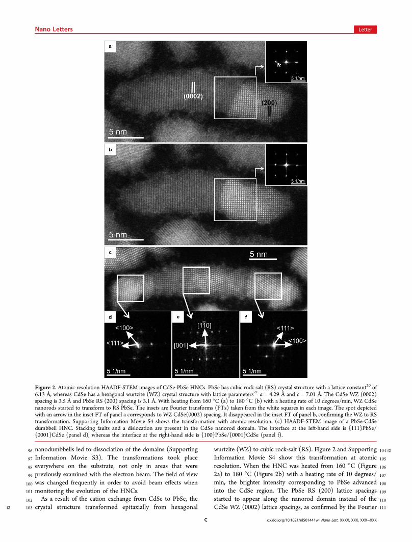
f2 103 crystal structure transformed epitaxially from hexagonal
104 f2wurtzite (WZ) to cubic rock-salt (RS). Figure 2 and Supporting105Information Movie S4 show this transformation at atomic106resolution. When the HNC was heated from 160 °C (Figure1072a) to 180 °C (Figure 2b) with a heating rate of 10 degrees/108min, the brighter intensity corresponding to PbSe advanced109into the CdSe region. The PbSe RS (200) lattice spacings110started to appear along the nanorod domain instead of the111CdSe WZ (0002) lattice spacings, as confirmed by the Fourier
Figure 2. Atomic-resolution HAADF-STEM images of CdSe-PbSe HNCs. PbSe has cubic rock salt (RS) crystal structure with a lattice constant20 of6.13 Å, whereas CdSe has a hexagonal wurtzite (WZ) crystal structure with lattice parameters21 a = 4.29 Å and c = 7.01 Å. The CdSe WZ (0002)spacing is 3.5 Å and PbSe RS (200) spacing is 3.1 Å. With heating from 160 °C (a) to 180 °C (b) with a heating rate of 10 degrees/min, WZ CdSenanorods started to transform to RS PbSe. The insets are Fourier transforms (FTs) taken from the white squares in each image. The spot depictedwith an arrow in the inset FT of panel a corresponds to WZ CdSe(0002) spacing. It disappeared in the inset FT of panel b, confirming the WZ to RStransformation. Supporting Information Movie S4 shows the transformation with atomic resolution. (c) HAADF-STEM image of a PbSe-CdSedumbbell HNC. Stacking faults and a dislocation are present in the CdSe nanorod domain. The interface at the left-hand side is {111}PbSe/{0001}CdSe (panel d), whereas the interface at the right-hand side is {100}PbSe/{0001}CdSe (panel f).
Nano Letters Letter
dx.doi.org/10.1021/nl501441w | Nano Lett. XXXX, XXX, XXX−XXXC
112 transformation (FT) patterns shown in the insets. It is clear113 that the cation exchange takes place at the PbSe/CdSe interface114 and propagates epitaxially (layer by layer) along the WZ ⟨0001⟩115 direction. Two types of interfaces were observed: {100}PbSe/116 {0001}CdSe and {111}PbSe/{0001}CdSe, similar to the117 interfaces previously reported in the literature for PbSe/CdSe118 and PbS/CdS HNCs.7,19 Sometimes both types of interfaces119 were observed within one single dumbbell NC. Figure 2c shows120 a HNC with the interfaces of {111}PbSe/{0001}CdSe on the121 left (Figure 2d) and {100}PbSe/{0001}CdSe on the right122 (Figure 2f). It is clear from Figure 2 that epitaxial PbSe growth123 inside CdSe domain via cation exchange can advance from both124 PbSe/CdSe interfaces.125 Considering the source of Pb that is required for the epitaxial126 PbSe growth in CdSe via cation exchange, we note that PbSe127 NCs with excess Pb surface atoms (off-stoichiometric) have128 been reported in the literature.22−24 Pb atoms (possibly Pb-129 oleate molecules) are also present along the CdSe nanorods130 (Figure 1f). From the quantification of the elemental maps (see131 Methods and Supporting Information Table S1), it was found132 that the PbSe tips contained an excess of Pb, having a cation/133 anion ratio of 1.3 ± 0.2. After the transformation, the cation/134 anion ratio at these PbSe tips reduced to 1.02 ± 0.14. These135 findings indicate Pb diffusion from PbSe tips toward the PbSe/136 CdSe interface. Supporting Information Movie S4 verifies this,137 whereby the bright Pb contrast propagates into the initially138 CdSe nanorod, indicating the epitaxial growth of PbSe, whereas139 the (PbSe) tip domain starts to lose some of its brightness,140 indicating that excess Pb is consumed.141 In the nanorod domains attached to the PbSe tips where142 cation exchange took place, the cation/anion ratio in the rod143 was reduced to 0.93 ± 0.11 due to Cd sublimation. That most144 nanodumbbells were not completely transformed must, hence,145 be due to the depletion of the source of Pb. The excess Pb146 atoms at the surfaces of the heteronanointerface diffuse toward147 the interface to form new layers of PbSe, but this process stops148 when all excess Pb has been depleted. As mentioned above, a149 complete transformation of the nanorods occurred only rarely.
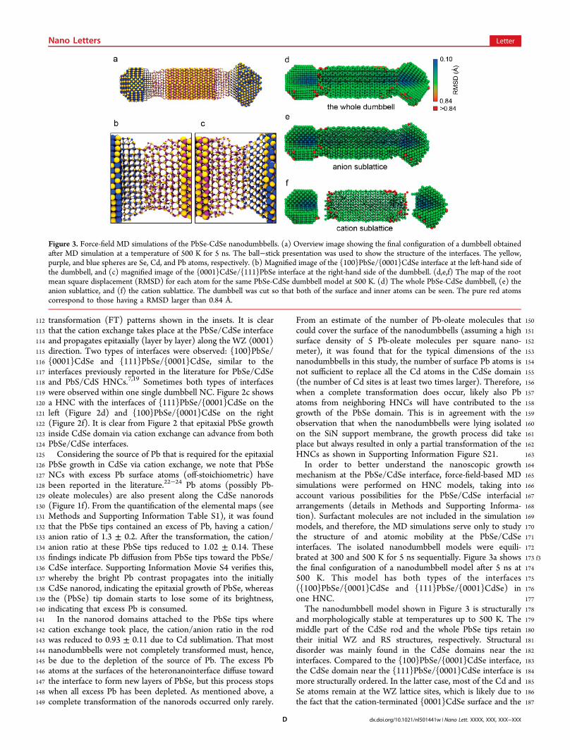
150From an estimate of the number of Pb-oleate molecules that151could cover the surface of the nanodumbbells (assuming a high152surface density of 5 Pb-oleate molecules per square nano-153meter), it was found that for the typical dimensions of the154nanodumbbells in this study, the number of surface Pb atoms is155not sufficient to replace all the Cd atoms in the CdSe domain156(the number of Cd sites is at least two times larger). Therefore,157when a complete transformation does occur, likely also Pb158atoms from neighboring HNCs will have contributed to the159growth of the PbSe domain. This is in agreement with the160observation that when the nanodumbbells were lying isolated161on the SiN support membrane, the growth process did take162place but always resulted in only a partial transformation of the163HNCs as shown in Supporting Information Figure S21.164In order to better understand the nanoscopic growth165mechanism at the PbSe/CdSe interface, force-field-based MD166simulations were performed on HNC models, taking into167account various possibilities for the PbSe/CdSe interfacial168arrangements (details in Methods and Supporting Informa-169tion). Surfactant molecules are not included in the simulation170models, and therefore, the MD simulations serve only to study171the structure of and atomic mobility at the PbSe/CdSe172interfaces. The isolated nanodumbbell models were equili-173 f3brated at 300 and 500 K for 5 ns sequentially. Figure 3a shows174the final configuration of a nanodumbbell model after 5 ns at175500 K. This model has both types of the interfaces176({100}PbSe/{0001}CdSe and {111}PbSe/{0001}CdSe) in177one HNC.178The nanodumbbell model shown in Figure 3 is structurally179and morphologically stable at temperatures up to 500 K. The180middle part of the CdSe rod and the whole PbSe tips retain181their initial WZ and RS structures, respectively. Structural182disorder was mainly found in the CdSe domains near the183interfaces. Compared to the {100}PbSe/{0001}CdSe interface,184the CdSe domain near the {111}PbSe/{0001}CdSe interface is185more structurally ordered. In the latter case, most of the Cd and186Se atoms remain at the WZ lattice sites, which is likely due to187the fact that the cation-terminated {0001}CdSe surface and the
Figure 3. Force-field MD simulations of the PbSe-CdSe nanodumbbells. (a) Overview image showing the final configuration of a dumbbell obtainedafter MD simulation at a temperature of 500 K for 5 ns. The ball−stick presentation was used to show the structure of the interfaces. The yellow,purple, and blue spheres are Se, Cd, and Pb atoms, respectively. (b) Magnified image of the {100}PbSe/{0001}CdSe interface at the left-hand side ofthe dumbbell, and (c) magnified image of the {0001}CdSe/{111}PbSe interface at the right-hand side of the dumbbell. (d,e,f) The map of the rootmean square displacement (RMSD) for each atom for the same PbSe-CdSe dumbbell model at 500 K. (d) The whole PbSe-CdSe dumbbell, (e) theanion sublattice, and (f) the cation sublattice. The dumbbell was cut so that both of the surface and inner atoms can be seen. The pure red atomscorrespond to those having a RMSD larger than 0.84 Å.
Nano Letters Letter
dx.doi.org/10.1021/nl501441w | Nano Lett. XXXX, XXX, XXX−XXXD
188 anion-terminated {111}PbSe surface form a continuous polar/189 polar interface, whereas the lattice mismatch is small. In190 contrast, the {100}PbSe/{0001}CdSe interface is a nonpolar/191 polar interface, which leads to stronger distortions in the atomic192 lattice due to Coulombic interactions. The simulations193 therefore suggest that the transformation at the {100}PbSe/194 {0001}CdSe interface will be more efficient than at the195 {111}PbSe/{0001}CdSe interface, although this could not be196 confirmed by the experiments as the orientation of the two197 crystals could be determined only in a limited number of cases.198 Not only is the atomic structure more disordered in the CdSe199 domains near the {100}PbSe/{0001}CdSe interfaces (see200 Supporting Information Figure S22 for a planar view of the201 atomic bilayers parallel to the interface), the simulations also202 show an unusually high mobility of the Cd atoms in the few203 first atomic layers from the PbSe/CdSe interface, as evidenced204 by the map of the root mean square displacement (RMSD) for205 each atom (Figure 3d−f). Those atoms with the highest206 mobility (red atoms) are mostly Cd atoms near the interfaces207 or on the surface, indicating that the cation exchange occurs208 only very close to the interface.209 The experimental observations and the MD simulations210 suggest that the transformation is mediated by vacancies in the211 Cd and Pb sublattices; evaporation of Cd results in Cd212 vacancies at the CdSe surface. After migration of these Cd213 vacancies to the PbSe/CdSe interface, Pb atoms can jump into214 the vacant sites, thereby leaving behind vacancies on the Pb215 sublattice, which will eventually recombine with excess Pb216 absorbed at the surface of the PbSe domain. Density functional217 theory (DFT) calculations of defect energies (see Section F in218 Supporting Information) confirm that upon evaporation of Cd,219 both in CdSe and PbSe the defect energetics are ruled by220 vacancies. The DFT calculations also show (Supporting221 Information Table S10) that the Se-Frenkel defect energy (Se222 vacancy + Se interstitial) is considerably higher (6.00 for CdSe223 and 3.80 eV for PbSe) than the Cd-Frenkel and Pb-Frenkel224 defect energies (3.16 and 3.30 eV, respectively). It is, thus,225 energetically much more expensive to create defects on the Se226 sublattice. Because the Se sublattice is not much affected by the227 cation exchange that takes place on the (Pb,Cd) sublattice, the228 crystallographic orientation relation between the CdSe and229 PbSe nanodomains is retained during the transformation. This230 is the reason that the growth process is epitaxial in nature.231 The most important driving force for the growth process is232 the evaporation of Cd. It is well known that a chemical reaction233 can be efficiently driven into one direction by bringing one234 reaction product in the gas phase. Assuming that the excess Pb235 originates from Pb-oleate coverage of the HNC and that the Cd236 evaporates in a molecular form, the chemical reaction can be237 summarized as follows:
+ ‐ → + ‐CdSe(s) Pb molecule(s) PbSe(s) Cd molecule(g)238 (1)
239 In the CdSe lattice, the Cd and Se atoms can be modeled as240 ions. Bader charge analysis (details in Section E of the241 Supporting Information) performed on the electronic charge242 density obtained from DFT calculations shows that the effective243 charge of the Cd cation in CdSe bulk is approximately +0.8e.244 However, the Cd will evaporate only as a neutral species.245 Because the transition from a charged Cd+0.8 ion to a neutral246 Cd0 atom would require the nanocrystal to donate electrons,247 we consider it more likely that Cd at the surface of the248 nanocrystal binds to the surfactants (e.g., oleate), followed by
249evaporation. We mention here that heating in vacuum is an250efficient method to detach surfactants from nanocrystals.20,25
251From the available experimental and simulation data, a252mechanism can now be deduced to describe the cation253exchange. All processes take place close to the interfaces in a254fast and volatile manner as demonstrated by Supporting255Information Movie S4. The growth mechanism is shown256schematically in Figure S1 of the Supporting Information and257can be summarized as follows. (i) Cd sublimates from the258surface of the CdSe nanodomains, whereby Cd vacancies are259formed. (ii) The Cd vacancies occupy positions at the CdSe260side of the PbSe/CdSe interface (Figure 3 and Supporting261Information Figure S22). (iii) Cation replacement takes place262as Pb atoms jump into vacant Cd sites in a layer by layer263fashion, resulting in epitaxial growth of RS PbSe at the expense264of WZ CdSe. (iv) The jumping Pb atoms leave behind265vacancies, which migrate to the PbSe surface. (v) The Pb266vacancies at the surface recombine with Pb ions from adsorbed267Pb-oleate molecules. The oleate molecule remains adsorbed at268the PbSe surface and possibly migrates to the CdSe domain269where it combines with Cd and evaporates as Cd-oleate. (vi)270The process is halted when the excess Pb (in the form of Pb-271oleate molecules) in the system is depleted.272The atomistic mechanism described here most likely also273takes place when HNCs undergo cation exchange in colloidal274solutions, whereby instead of evaporating, the metal-molecule275complex is dissolved in the solution. In the current solid−276solid−vapor (SSV) growth mechanism, one solid phase grows277epitaxially at the expense of another solid phase, efficiently278driven by evaporation of one element (here, Cd) with279simultaneous supply of another element (here, Pb coordinated280with a molecule). Our results show that SSV growth can281provide an alternative path for growing heterogeneous282semiconductor nanowires, especially when the lattices have a283partly ionic character, and therefore holds promise for284generating new families of heterogeneous nanostructures.
285■ METHODS286The synthesis of PbSe/CdSe dumbbell nanostructures is287detailed in the Supporting Information. TEM specimens were288prepared by dropcasting 8 μL of the NC colloidal solution onto289a MEMS microhot plate with electron-transparent SiN290membranes, which was mounted onto a DENSsolutions low291drift TEM heating holder.25 After dropcasting, the sample was292plasma cleaned for 10 s in order to remove deposits from the293solution that prevent high-resolution imaging in the TEM. The294in situ experiments were performed in a 80−300 FEI Titan295microscope equipped with a Chemi-STEM EDX detection296system. During HAADF-STEM imaging, the microscope was297operated at 300 kV. The camera length used in the experiments298equals 91 mm in order to avoid diffraction effects and to299guarantee Z-contrast imaging. In HAADF-STEM imaging, the300intensity approximately scales with Z2. As Pb has a higher Z301number than Cd, the PbSe domains appear with higher302intensity in HAADF-STEM images in comparison to the CdSe303domains.304The Chemi-STEM EDS experiments were performed using305the same holder and in the same 80−300 FEI Titan microscope306but were operated at a lower acceleration voltage of 200 kV to307reduce beam damage during mapping. A beam current of308approximately 250 pA was used during acquisition. A309representative spectrum is shown in Supporting Information310Supplementary Figure S20. In the quantification of the
Nano Letters Letter
dx.doi.org/10.1021/nl501441w | Nano Lett. XXXX, XXX, XXX−XXXE
311 elemental maps, 18 PbSe NC maps were used to determine the312 cation/anion ratio at the PbSe tips at the initial state. For the313 PbSe tips from where cation exchange proceeded, the elemental314 composition of 10 different PbSe tips was quantified. For the315 nanorod domains attached to the PbSe tips where cation316 exchange took place, the elemental composition of 10 different317 nanorod (transformed)-domains were quantified. Additional318 TEM images, chemical maps, and quantitative analysis are319 provided in Figures S2−S19 and Tables S1−S6 of the320 Supporting Information.321 For the force-field MD simulations, a new interaction322 potential model for the Pb−Cd−Se system was developed.323 The potential was found to accurately describe physical324 parameters such as lattice parameters, elastic constants, and325 the relative stability of phases. Details of the potential model326 (Supporting Information Table S7) and a description of the327 nanodumbbell models are given in Section E of the Supporting328 Information. For simulations of the nanodumbbells, Coulomb329 and short-range interactions were calculated by taking into330 account all atom pairs. The equations of motion were331 integrated using the velocity Verlet algorithm with a time332 step of 1 fs. Periodic boundary conditions were not used and333 the nanodumbbell models were isolated in vacuum. Simulations334 of 5 ns were carried out in the NVT ensemble and 1 ns was335 used for equilibration.336 All density functional theory (DFT) calculations on defect337 energies and energies of mixed PbSe-CdSe phases were carried338 out using the first-principles’ Vienna Ab Initio Simulation339 Program (VASP)26 using the projector augmented wave340 (PAW) method.27 The generalized gradient approximation341 (GGA) formulated by Perdew, Burke, and Ernzerhof (PBE)342 was employed for the exchange and correlation energy terms.28
343 The cutoff energy of the wave functions was 350.0 eV. The344 cutoff energy of the augmentation functions was about 500.0345 eV. The electronic wave functions were sampled on a 4 × 4 × 2346 grid using the Monkhorst and Pack method with 8 to 20 k-347 points depending on different symmetries of supercells (108348 atoms). Structural optimizations were performed for both349 lattice parameters and coordinates of atoms. Different k-meshes350 and cutoff energies for waves were tested to have a good351 convergence (<2 meV/atom). Details are given in the352 Supporting Information.
353 ■ ASSOCIATED CONTENT
354 *S Supporting Information355 Includes four movies (Movies S1, S2, S3, and S4), a description356 of the synthesis of the PbSe/CdSe HNCs, additional HAADF-357 STEM images, STEM-EDX chemical maps and quantification,358 force field MD simulations, and DFT calculations of the defect359 energies and mixed PbSe-CdSe phases. This material is360 available free of charge via the Internet at http://pubs.acs.org.
361 ■ AUTHOR INFORMATION
362 Corresponding Author363 *E-mail: [email protected].
364 Author Contributions¶
365 These authors contributed equally.
366 Notes367 The authors declare no competing financial interest.
368■ ACKNOWLEDGMENTS
369This work is part of the research programme of the Foundation370for Fundamental Research on Matter (FOM), which is part of371The Netherlands Organization for Scientific Research (NWO).372A.O.Y. and F.D.T. acknowledge European Soft Matter373Infrastructure (ESMI) for Transnational Access Grant.374DENSsolutions is acknowledged for providing MEMS based375microhot plates and the low-drift TEM heating holder.376Computational resources were supported by NWO Exacte377Wetenschappen (Physical Sciences). This work was also378sponsored by the Stichting Nationale Computerfaciliteiten379(National Computing Facilities Foundation, NCF) for the use380of supercomputing facilities, with financial support from NWO.381M.A.v.H. acknowledges a VIDI grant from NWO. The authors382acknowledge financial support from European Research383Council (ERC Advanced Grant No. 24691-COUNTATOMS,384ERC Starting Grant No. 335078-COLOURATOMS). This385work was supported by the Flemish Fund for Scientific386Research (FWO Vlaanderen) through a Ph.D. research grant387to B.G.
388■ REFERENCES(1) 389Son, D. H.; Hughes, S. M.; Yin, Y.; Alivisatos, A. P. Science 2004,
390306, 1009−1012.(2) 391Robinson, R. D.; Sadtler, B.; Demchenko, D. O.; Erdonmez, C.
392K.; Wang, L.-W.; Alivisatos, A. P. Science 2007, 317, 355−358.(3) 393Bals, S.; Casavola, M.; van Huis, M. A.; Van Aert, S.; Batenburg,
394K. J.; Van Tendeloo, G.; Vanmaekelbergh, D. Nano Lett. 2011, 11,3953420−3424.
(4) 396Casavola, M.; van Huis, M. A.; Bals, S.; Lambert, K.; Hens, Z.;397Vanmaekelbergh, D. Chem. Mater. 2012, 24, 294−302.
(5) 398Grodzin ska, D.; Pietra, F.; van Huis, M. A.; Vanmaekelbergh, D.;399de Mello Donega, C. J. Mater. Chem. 2011, 21, 11556−11565.
(6) 400Zhang, Y.; Dai, Q.; Li, X.; Cui, Q.; Gu, Z.; Zou, B.; Wang, Y.; Yu,401W. W. Nanoscale Res. Lett. 2010, 5, 1279−1283.
(7) 402Kudera, S.; Carbone, L.; Casula, M. F.; Cingolani, R.; Falqui, A.;403Snoeck, E.; Parak, W. J.; Manna, L. Nano Lett. 2005, 5, 445−449.
(8) 404Overgaag, K.; Evers, W.; de Nijs, B.; Koole, R.; Meeldijk, J.;405Vanmaekelbergh, D. J. Am. Chem. Soc. 2008, 130, 7833−7835.
(9) 406Grodzin ska, D.; Evers, W. H.; Dorland, R.; van Rijssel, J.; van407Huis, M. A.; Meijerink, A.; de Mello Donega, C.; Vanmaekelbergh, D.408Small 2011, 7, 3493−3501.
(10) 409van Huis, M. A.; Figuerola, A.; Fang, C.; Beche, A.; Zandbergen,410H. W.; Manna, L. Nano Lett. 2011, 11, 4555−4561.
(11) 411Figuerola, A.; van Huis, M.; Zanella, M.; Genovese, A.; Marras,412S.; Falqui, A.; Zandbergen, H. W.; Cingolani, R.; Manna, L. Nano Lett.4132010, 10, 3028−3036.
(12) 414De Trizio, L.; De Donato, F.; Casu, A.; Genovese, A.; Falqui, A.;415Povia, M.; Manna, L. ACS Nano 2013, 7, 3997−4005.
(13) 416Yalcin, A. O.; de Nijs, B.; Fan, Z.; Tichelaar, F. D.;417Vanmaekelbergh, D.; van Blaaderen, A.; Vlugt, T. J. H.; van Huis,418M. A.; Zandbergen, H. W. Nanotechnology 2014, 25, 055601.
(14) 419Wagner, R. S.; Ellis, W. C. Appl. Phys. Lett. 1964, 4, 89−90.(15) 420Gudiksen, M. S.; Lauhon, L. J.; Wang, J.; Smith, D. C.; Lieber,
421C. M. Nature 2002, 415, 617−620.(16) 422Wang, H.; Zepeda-Ruiz, L. A.; Gilmer, G. H.; Upmanyu, M. Nat.
423Commun. 2013, 4, 1956.(17) 424Persson, A. I.; Larsson, M. W.; Stenstrom, S.; Ohlsson, B. J.;
425Samuelson, L.; Wallenberg, L. R. Nat. Mater. 2004, 3, 677−681.(18) 426Campos, L. C.; Tonezzer, M.; Ferlauto, A. S.; Grillo, V.;
427Magalhaes-Paniago, R.; Oliveira, S.; Ladeira, L. O.; Lacerda, R. G. Adv.428Mater. 2008, 20, 1499−1504.
(19) 429Luther, J. M.; Zheng, H.; Sadtler, B.; Alivisatos, A. P. J. Am.430Chem. Soc. 2009, 131, 16851−16857.
Nano Letters Letter
dx.doi.org/10.1021/nl501441w | Nano Lett. XXXX, XXX, XXX−XXXF
(20)431 van Huis, M. A.; Kunneman, L. T.; Overgaag, K.; Xu, Q.;432 Pandraud, G.; Zandbergen, H. W.; Vanmaekelbergh, D. Nano Lett.433 2008, 8, 3959−3963.
(21)434 Xu, Y.-N.; Ching, W. Y. Phys. Rev. B: Condens. Matter Mater.435 Phys. 1993, 48, 4335−4351.
(22)436 Moreels, I.; Lambert, K.; De Muynck, D.; Vanhaecke, F.;437 Poelman, D.; Martins, J. C.; Allan, G.; Hens, Z. Chem. Mater. 2007, 19,438 6101−6106.
(23)439 Moreels, I.; Fritzinger, B.; Martins, J. C.; Hens, Z. J. Am. Chem.440 Soc. 2008, 130, 15081−15086.
(24)441 Petkov, V.; Moreels, I.; Hens, Z.; Ren, Y. Phys. Rev. B: Condens.442 Matter Mater. Phys. 2010, 81, 241304.
(25)443 van Huis, M. A.; Young, N. P.; Pandraud, G.; Creemer, J. F.;444 Vanmaekelbergh, D.; Kirkland, A. I.; Zandbergen, H. W. Adv. Mater.445 2009, 21, 4992−4995.
(26)446 Kresse, G.; Hafner, J. Phys. Rev. B: Condens. Matter Mater. Phys.447 1993, 47, 558−561.
(27)448 Kresse, G.; Joubert, D. Phys. Rev. B: Condens. Matter Mater. Phys.449 1999, 59, 1758−1775.
(28)450 Perdew, J. P.; Burke, K.; Ernzerhof, M. Phys. Rev. Lett. 1996, 77,451 3865−3868.
Nano Letters Letter
dx.doi.org/10.1021/nl501441w | Nano Lett. XXXX, XXX, XXX−XXXG
Copyright © 2022 FDOKUMEN