Structural characterization of chemically synthesized CdSe nanoparticles
6
Structural characterization of chemically synthesized CdSe nanoparticles M.F. Kotkata a, , A.E. Masoud b , M.B. Mohamed c , E.A. Mahmoud b a Physics Department, Faculty of Science, Ain Shams University, Cairo 11566, Egypt b Physics Department, Faculty of Science, Al-Azhar University for Girls, Cairo 11884, Egypt c National Institute of Laser Enhanced Sciences (NILES), Cairo University, Cairo, Egypt article info Article history: Received 12 September 2008 Received in revised form 22 October 2008 Accepted 27 October 2008 Available online 25 November 2008 PACS: 81.05.Dz 81.07.b 81.07.Bc 81.16.Be 81.70.Pg Keywords: CdSe Nanoparticles Synthesis Confinement effect Chalcogenides Semiconductors II–VI group abstract CdSe nanoparticles were prepared at room-temperature via direct reaction between Cd(NO 3 ) 2 and Na 2 Se in the presence of cetyltrimethyl ammonium bromide (CTAB) used as a capping material. The nanoparticles were characterized by X-ray diffraction (XRD), transmission electron microscopy (TEM), UV-Visible absorption spectrum, Fourier transform infrared (FT-IR) spectroscopy, Raman scattering, differential scanning calorimetry (DSC), differential thermal gravimetric (DTG) and heat stage X-ray diffraction (HS-XRD). Analysis of the obtained data reveals the precipitation of defective zinc blende CdSe nanoparticles of size about 11nm in diameter. A blue shift in the optical gap, from 1.71 to 1.82eV, has been observed for the absorption spectrum of the synthesized CdSe nanoparticles, as an indication of quantum confinement effect. The zinc blende phase is enhanced upon annealing above the melting of Se (220 1C) as is transformed into a better order and stable wurtzite structure upon further heating. More than one melting point has been recorded for the CdSe nanoparticles referring to different ranges of particle sizes (7:25nm). A value of 810 1C characterizes the melting point of the predominant size (11 nm) of the CdSe nanoparticles. & 2008 Published by Elsevier B.V. 1. Introduction Nanoparticles have been investigated intensively in the past two decades because of their size-dependent properties and the possibility of arranging them in micro (and nano) assemblies [1–3]. Selenides have been widely used as thermoelectric cooling materials, optical filter, optical recording materials, solar cells, superionic materials, biological sensor and laser materials [4–6]. Nanoparticles of selenide semiconductors were attracting the attention due to their brilliant prospects. In particular, nanos- tructures of CdSe have received considerably more attention due to its great fundamental, experimental and applied interests. Indeed, CdSe nanocrystals are useful in understanding the phenomenon of quantum confinement effect as are used in the fabrication of devices like PV cells, lasers, TFTs, Light-emitting diodes and other nanoscale devices [7]. In the past few years, there have been several reports on the synthesis of CdSe nanoparticles. CdSe nanoparticles were success- fully synthesized by organometallic approach [8–10]. Such a procedure requires expensive chemicals and resulting in the production of small amounts of colloidal nanoparticles. Besides, the nanoparticles prepared in organic phase are insoluble in water, and, therefore, cannot be directly applied in bio-systems. The synthesis in aqueous phase is an alternative method for the preparation of nanoparticles. Compared with organic phase synthesis, aqueous synthesis exhibits good reproducibility, low toxicity and inexpensive; besides that the products have excellent water-solubility, stability and biological compatibility [11,12]. In literature, few reports were found about the synthesis of nanoparticles such as CdS [13,14] and CdSe [12,15] in water phase. Therefore, our attention in the present paper became focused on developing a relatively cheap, yet effective, method for achieving of the CdSe nanoparticles. This has been done via a direct reaction between Cd(NO 3 ) 2 and Na 2 Se in the presence of cetyltrimethyl ammonium bromide (CTAB), which is used as a capping agent. The structural characterization of the synthesized material is accurately considered. ARTICLE IN PRESS Contents lists available at ScienceDirect journal homepage: www.elsevier.com/locate/physe Physica E 1386-9477/$ - see front matter & 2008 Published by Elsevier B.V. doi:10.1016/j.physe.2008.10.019 Corresponding author. E-mail address: [email protected] (M.F. Kotkata). Physica E 41 (2009) 640–645
-
Upload
independent -
Category
Documents
-
view
1 -
download
0
Transcript of Structural characterization of chemically synthesized CdSe nanoparticles

ARTICLE IN PRESS
Physica E 41 (2009) 640–645
Contents lists available at ScienceDirect
Physica E
1386-94
doi:10.1
� Corr
E-m
journal homepage: www.elsevier.com/locate/physe
Structural characterization of chemically synthesized CdSe nanoparticles
M.F. Kotkata a,�, A.E. Masoud b, M.B. Mohamed c, E.A. Mahmoud b
a Physics Department, Faculty of Science, Ain Shams University, Cairo 11566, Egyptb Physics Department, Faculty of Science, Al-Azhar University for Girls, Cairo 11884, Egyptc National Institute of Laser Enhanced Sciences (NILES), Cairo University, Cairo, Egypt
a r t i c l e i n f o
Article history:
Received 12 September 2008
Received in revised form
22 October 2008
Accepted 27 October 2008Available online 25 November 2008
PACS:
81.05.Dz
81.07.�b
81.07.Bc
81.16.Be
81.70.Pg
Keywords:
CdSe
Nanoparticles
Synthesis
Confinement effect
Chalcogenides
Semiconductors
II–VI group
77/$ - see front matter & 2008 Published by
016/j.physe.2008.10.019
esponding author.
ail address: [email protected] (M.F. Kotkata).
a b s t r a c t
CdSe nanoparticles were prepared at room-temperature via direct reaction between Cd(NO3)2 and
Na2Se in the presence of cetyltrimethyl ammonium bromide (CTAB) used as a capping material. The
nanoparticles were characterized by X-ray diffraction (XRD), transmission electron microscopy (TEM),
UV-Visible absorption spectrum, Fourier transform infrared (FT-IR) spectroscopy, Raman scattering,
differential scanning calorimetry (DSC), differential thermal gravimetric (DTG) and heat stage X-ray
diffraction (HS-XRD).
Analysis of the obtained data reveals the precipitation of defective zinc blende CdSe nanoparticles of
size about 11 nm in diameter. A blue shift in the optical gap, from 1.71 to 1.82 eV, has been observed for
the absorption spectrum of the synthesized CdSe nanoparticles, as an indication of quantum
confinement effect. The zinc blende phase is enhanced upon annealing above the melting of Se
(220 1C) as is transformed into a better order and stable wurtzite structure upon further heating. More
than one melting point has been recorded for the CdSe nanoparticles referring to different ranges of
particle sizes (7:25 nm). A value of 810 1C characterizes the melting point of the predominant size
(11 nm) of the CdSe nanoparticles.
& 2008 Published by Elsevier B.V.
1. Introduction
Nanoparticles have been investigated intensively in the pasttwo decades because of their size-dependent properties and thepossibility of arranging them in micro (and nano) assemblies[1–3].
Selenides have been widely used as thermoelectric coolingmaterials, optical filter, optical recording materials, solar cells,superionic materials, biological sensor and laser materials [4–6].Nanoparticles of selenide semiconductors were attracting theattention due to their brilliant prospects. In particular, nanos-tructures of CdSe have received considerably more attention dueto its great fundamental, experimental and applied interests.Indeed, CdSe nanocrystals are useful in understanding thephenomenon of quantum confinement effect as are used in thefabrication of devices like PV cells, lasers, TFTs, Light-emittingdiodes and other nanoscale devices [7].
Elsevier B.V.
In the past few years, there have been several reports on thesynthesis of CdSe nanoparticles. CdSe nanoparticles were success-fully synthesized by organometallic approach [8–10]. Such aprocedure requires expensive chemicals and resulting in theproduction of small amounts of colloidal nanoparticles. Besides,the nanoparticles prepared in organic phase are insoluble inwater, and, therefore, cannot be directly applied in bio-systems.The synthesis in aqueous phase is an alternative method for thepreparation of nanoparticles. Compared with organic phasesynthesis, aqueous synthesis exhibits good reproducibility, lowtoxicity and inexpensive; besides that the products have excellentwater-solubility, stability and biological compatibility [11,12]. Inliterature, few reports were found about the synthesis ofnanoparticles such as CdS [13,14] and CdSe [12,15] in water phase.
Therefore, our attention in the present paper became focusedon developing a relatively cheap, yet effective, method forachieving of the CdSe nanoparticles. This has been done via adirect reaction between Cd(NO3)2 and Na2Se in the presence ofcetyltrimethyl ammonium bromide (CTAB), which is used as acapping agent. The structural characterization of the synthesizedmaterial is accurately considered.

ARTICLE IN PRESS
M.F. Kotkata et al. / Physica E 41 (2009) 640–645 641
2. Experimental
2.1. Synthesis
Typically, 4.96 g of Cd(NO3)2 �4H2O {Riedel-de Haen, 99%} and2.5 g of CTAB {PARK-Scientific Limited, 99%} were dissolved in100 mL of re-distilled water under stirring at room-temperature(RT�25 1C). In another flask, 2 g of Na2Se {Alfa Aesar, 99.8%} wasdissolved in 100 mL of re-distilled water, and then added to theformer solution while stirring; i.e.,
CdðNO3Þ2 þ Na2Se! CdSeþ 2ðNa2NO3Þ
Once the reaction took place, the solution was filtered, washedseveral times (5–10 times) by re-distilled water, and left in a darkand dry place till complete dryness.
2.2. Measurements
The structure and the phase changes of the synthesized CdSesample were examined by BRUKER D8 ADVANCE heat stage X-raydiffraction (HS-XRD) using CuKa (l ¼ 0.15406 nm), at a powerof 1600 W (40 kV and 40 mA). For heat stages, heating rate at601/min was used.
Transmission electron microscope (TEM), type 1230 JOEL,operating at power ¼ 100 kV has been used for data collection. Forobtaining the TEM images, the as-prepared sample was dispersed inabsolute ethanol ultrasonically and then the colloid was droppedonto Cu-grids coated with amorphous carbon film and dried.
UV-visible spectrum of the as-prepared sample was recordedusing Bio-Cary50 Model spectrophotometer in the wavelengthrange 300–900 nm. The sample was suspended in re-distilledwater, which has been used as a blank in setting up the base line.A quartz cell has been used as a sample container.
A Fourier transform infrared (FT-IR) spectroscopy and Ramanmeasurements were carried out using FT-IR Raman JASCO (6300Type A).
The differential scanning calorimetry (DSC) curves were recordedusing SETARAM analyzer (LabsysTM TG DSC1) with heating ratesof 5–101/min in the temperature range: RT-1000 1C. Differentialthermal gravimetric (DTG) curve was recorded using Shimadzuanalyzer (model DTG-60/60A) with a heating rate of 101/min.
3. Results and discussion
3.1. XRD analyses
The XRD pattern of the as-prepared CdSe sample is shown inFig. 1. The figure shows that the intensity of the characteristicdiffraction lines is rather low as accompanied by a relatively highbackground pattern. This indicates that the diffraction pattern ofFig. 1 exhibited a poor crystalline structure. Here, the pattern ischaracterized by the presence of three groups of diffraction lines.
20
Inte
nsity
(a.u
.)
2θ (degree)
Se (ICCD 86-2244)
30 40 50 60 70 80 90
Fig. 1. XRD pattern of the as-prepared CdSe nanoparticles.
These groups lie over the area of what is called a stepped-hump inthe corresponding amorphous phase. In other words, theseangular ranges correspond to numerous lattice directions oratomic planes of high scattering power in the respective crystal-line forms. The stepped-hump areas roughly occupy the angularranges: (21:37), (37:46) and (46:54) in 2y for the first, second andthird step, respectively. These three steps have their respectivemaxima at about 261, 431 and 501.
Identification of the observed diffraction peaks in Fig. 1declares the presence of CdSe zinc blende structure (see the ICCDCard no. 19-0191). However, such a diffraction pattern isconsidered to be a defective crystal structure. This is due, mainly,to the appearance of the three-stepped-hump together with theappearance of a clear selenium peak. The Se peak appeared at2y ¼ 30.3581, attributed to the (10 1) plane, which is the preferredorientation of the Se hexagonal structure. This was concluded byreferring to the ICCD Card no. 86-2244.
In fact, the presence of a Se peak in the synthesized CdSesample could be attributed to the possibility of forming H2Seduring the dissolution of Na2Se in accord with the followingequation:
Na2SeþH2O! NaOHþH2Se
Hence, the presence of H2Se in an aqueous NO3�media enhances
the formation of pure Se.The average crystalline size, that was determined from the
half-width of the diffraction peaks using the Debye–Scherrerequation, was approximately 5 nm in diameter for the CdSenanoparticles, while it was about 55 nm for Se nanoparticles.
3.2. TEM observation
Fig. 2 presents TEM images of the size distribution of the as-prepared material. The left image, shown in Fig. 2(a), focuses onthe Se particles. This photo shows the existence of Se nanopar-ticles with sizes lying in the range 40:80 nm, while most of themhave size of about 60 nm. The other image, shown in Fig. 2(b),focuses on CdSe nanoparticles. It can be concluded from thisphoto that the particle size ranges from 7 to 25 nm, while most ofthem have a size of about 11 nm.
3.3. UV–visible absorption spectrum
The most dramatic property of semiconductor nanoparticles isthe size evolution of the optical absorption spectra. In this respect,Fig. 3 shows the absorption spectrum of the nanoparticles ofCdSe. The figure shows that the recorded spectrum exhibits anabsorption edge having its onset at �685 nm. This corresponds toan energy gap of �1.82 eV. The edge is assigned to the opticaltransition of the first excitonic state. Generally, the wavelengthof the exciton absorption band decreases with decreasing theparticle size as a result of quantum confinement of the photo-generated electron–hole pairs.
In fact, the value of the energy gap, estimated from Fig. 3,reflects a considerable blue shift relative to the absorption bandedge of bulk CdSe (725 nm and 1.71 eV), [16]. The grain size ofsemiconductor nanoparticles can be determined using Brusequation [17]
Enanog � Ebulk
g ¼h2
8r2
1
m�eþ
1
m�h
!�
1:8e2
4p��or� 0:248E�Ry
where Egnano and Eg
bulk are the respective nanoparticles and bulkenergy band gaps, r is the radius of the particle, m*e & m*h are thereduced masses of the conduction band electron and valence bandhole in units of electron mass, eo is the vacuum permittivity, e is

ARTICLE IN PRESS
Fig. 2. TEM photos for the as-prepared CdSe sample with MP: 80,000 (a) and with MP: 1,00,000 (b).
625
685 nm
Abs
orpt
ion
(a.u
.)
Wavelength (nm)650 675 700 725
Fig. 3. UV–vis. absorption spectrum of the synthesized CdSe nanoparticles.
4000
(CH
2 st
retc
hing
)
700
(Cd-
Se
stre
tchi
ng)
840
(=C
-H &
=C
H2
out-o
f-pla
ne b
endi
ng)
890
950
(NH
2 &
N-H
ben
ding
)10
40 (C
-C s
tretc
hing
)13
65 (C
H3
bend
ing
defo
rmed
)
1445
(C-N
stre
tchi
ng)
1615
(NH
2 sc
isso
ring)
2845
2910
30
10 (C
-H s
tretc
hing
)
3420
(NH
2 st
retc
hing
)
Abs
orpt
ion
(a.u
.) %
Wavenumber (cm-1)
3500 3000 2500 2000 1500 1000 500
Fig. 4. FT-IR (whole scale) for the as-prepared CdSe nanoparticles.
M.F. Kotkata et al. / Physica E 41 (2009) 640–645642
the high-frequency dielectric constant, and E*Ry is the effectiveRydberg energy given by
E�Ry ¼e4
2�2h2
1
m�eþ
1
m�h
!�I
Applying the previously mentioned Brus’ equation, a value�10 nm has been estimated for the nanoparticles size of thesynthesized CdSe sample.
That is the particle size calculated from the absorptionspectrum, for the CdSe phase, is in a good agreement with whathas been estimated from the TEM images, while both valuesare twice that has been concluded from XRD. This insures theprediction of certain amount of amorphicity in the XRD of thesynthesized CdSe phase (Fig. 1). Hence, the CdSe peaks showmuch more broadening than it would be for nanocrystals, withhigh degree of crystallinity.
3.4. FT-IR and Raman spectra
Fig. 4 shows the FT-IR curve for the as-prepared CdSe sample.Assignments for the observed peaks are indicated on the chart,[18]. The main peak of Cd-Se stretching band has been observed at700 cm–1 [19]. All other peaks are corresponding to the structuralbonds of CTAB, specially those peaks observed at 3420, 3010, 2910and 2845 cm�1, which attributed to the respective NH2 stretchingand to the symmetry and asymmetry stretch vibration of CH2 ofCTAB molecule [20]. These latter peaks are considered as a proofof capping of the as-prepared CdSe nanoparticles by CTAB.
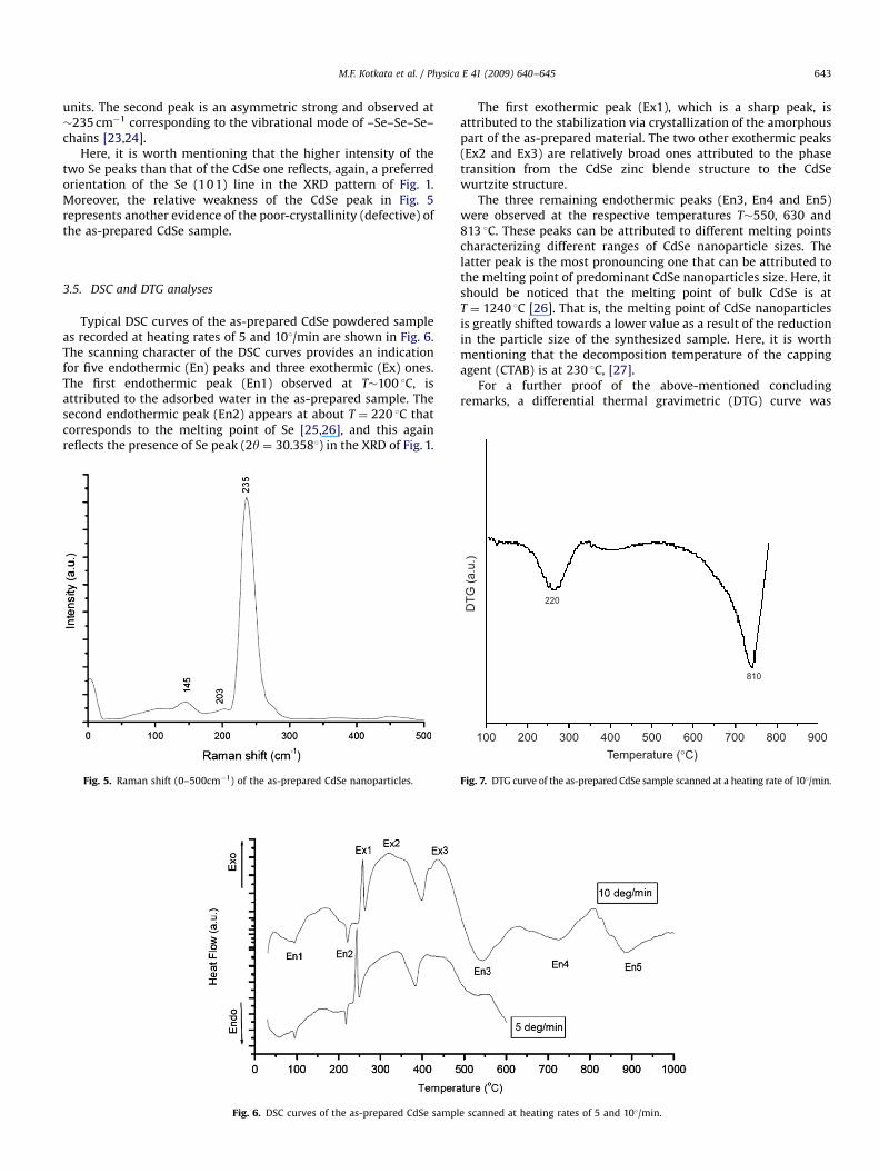
The recorded Raman spectrum of the synthesized CdSe nano-particles, in the range (0–500 cm�1), is shown in Fig. 5. Thespectrum exhibits a weak asymmetric band at about 203 cm�1
which attributed to the longitudinal optical (LO) phonon mode ofCdSe. This peak has been shifted from the LO mode of bulk CdSe(210 cm�1) [21], as a consequence of phonon confinement, [22].
Also, the recorded Raman spectrum shows two peaks corre-sponded to the Se phase. The first peak is a medium but broad andobserved at �145 cm�1, corresponding to the bending modes of Se
ARTICLE IN PRESS
M.F. Kotkata et al. / Physica E 41 (2009) 640–645 643
units. The second peak is an asymmetric strong and observed at�235 cm�1 corresponding to the vibrational mode of –Se–Se–Se–chains [23,24].
Here, it is worth mentioning that the higher intensity of thetwo Se peaks than that of the CdSe one reflects, again, a preferredorientation of the Se (10 1) line in the XRD pattern of Fig. 1.Moreover, the relative weakness of the CdSe peak in Fig. 5represents another evidence of the poor-crystallinity (defective) ofthe as-prepared CdSe sample.
3.5. DSC and DTG analyses
Typical DSC curves of the as-prepared CdSe powdered sampleas recorded at heating rates of 5 and 101/min are shown in Fig. 6.The scanning character of the DSC curves provides an indicationfor five endothermic (En) peaks and three exothermic (Ex) ones.The first endothermic peak (En1) observed at T�100 1C, isattributed to the adsorbed water in the as-prepared sample. Thesecond endothermic peak (En2) appears at about T ¼ 220 1C thatcorresponds to the melting point of Se [25,26], and this againreflects the presence of Se peak (2y ¼ 30.3581) in the XRD of Fig. 1.
Fig. 5. Raman shift (0–500cm�1) of the as-prepared CdSe nanoparticles.
Fig. 6. DSC curves of the as-prepared CdSe sampl
The first exothermic peak (Ex1), which is a sharp peak, isattributed to the stabilization via crystallization of the amorphouspart of the as-prepared material. The two other exothermic peaks(Ex2 and Ex3) are relatively broad ones attributed to the phasetransition from the CdSe zinc blende structure to the CdSewurtzite structure.
The three remaining endothermic peaks (En3, En4 and En5)were observed at the respective temperatures T�550, 630 and813 1C. These peaks can be attributed to different melting pointscharacterizing different ranges of CdSe nanoparticle sizes. Thelatter peak is the most pronouncing one that can be attributed tothe melting point of predominant CdSe nanoparticles size. Here, itshould be noticed that the melting point of bulk CdSe is atT ¼ 1240 1C [26]. That is, the melting point of CdSe nanoparticlesis greatly shifted towards a lower value as a result of the reductionin the particle size of the synthesized sample. Here, it is worthmentioning that the decomposition temperature of the cappingagent (CTAB) is at 230 1C, [27].
For a further proof of the above-mentioned concludingremarks, a differential thermal gravimetric (DTG) curve was
e scanned at heating rates of 5 and 101/min.
DTG
(a.u
.)
100 200 300 400 500 600 700 800 900Temperature (°C)
220
810
Fig. 7. DTG curve of the as-prepared CdSe sample scanned at a heating rate of 101/min.

ARTICLE IN PRESS
10
Se
2θ (degree)
as-prepared
w
zzz
w
z&wwIn
tens
ity (
a.u.
)
WW
WW W
WW
z&w
WWW
WWWW
W
WW
W W
W W
z&w
350 °C
300 °C
250 °C
200 °C
150 °C
20 30 40 50 60 70
Fig. 8. HS-XRD patterns of the as-prepared CdSe nanoparticles as treated at different heating stages.
(nm
)
30
25
20
M.F. Kotkata et al. / Physica E 41 (2009) 640–645644
recorded at 101/min and shown in Fig. 7. Analysis of the obtainedcurve proved the melting of Se at 220 1C. Moreover, the DTG curvegives an indication only for the melting point of CdSe at 810 1C,which supports the suggestion of its relation to the nanoparticleswith the predominant size.
Par
ticle
Siz
e
15
10
5
00 50 100 150 200 250 300 350
Temperature (°C)
230 °C)
Fig. 9. Least squares fit for the plot of particle size versus heating stage
temperature for CdSe nanoparticles.
3.6. HS-XRD analyses
Fig. 8 shows the effect of thermal annealing on the structure ofthe as-prepared CdSe sample at different heating stages: 150, 200,250, 300 and 350 1C.
According to the ICDD Card no. 19-0191, the CdSe zinc blendstructure completely appears after annealing at a temperature of150 1C. This can be easily identified by the appearance of threediffraction peaks at 2y ¼ 25.4591, 42.1091 and 49.6321 character-ized for the respective planes (111), (2 2 0) and (311).
At 200 1C, the XRD pattern of the sample has a mixture of twophases of CdSe, zinc blend (Z) with wurtzite (W). This can beidentified by the observation of the zinc blende lines, statedpreviously, together with new lines attributed to the wurtzitestructure. The new lines appeared at 2y ¼ 23.7271, 26.7911,42.3411 and 49.5671 correspond to the respective planes (10 0),(10 1), (110) and (11 2), as can be concluded from comparingthe observed 2y values with those indexed in the ICCD Card no.02-0330.
At an annealing temperature of 250 1C and above (300 and350 1C), the wurtzite structure of the CdSe phase is vastlyenhanced. This can be noticed from the rapid increase of the lineintensities together with the better resolution of the characteristicwurtzite diffraction peaks.
This means that the Se atoms, that appeared in the as-prepared(defective) material (Fig. (1)), are incorporated in the networkupon heating over 220 1C (Tm of Se), forming a stabilizedstoichiometric CdSe crystal. The structure of the latter is wurtzite.
On the other hand, such applied heat treatment scheme isaccompanied by an increase in the particle size of wurtzite CdSefrom �12 nm at 250 1C to �26 nm in diameter at 350 1C. Fig. 9shows a plot of the estimated values of the particle size as afunction of heating stage temperature of the as-prepared CdSesample. Here, the size values have been calculated using theDebye–Scherrer equation.
4. Conclusion
A detailed investigation for the structural characterization ofCdSe nanoparticles prepared at room-temperature via a directreaction between Cd(NO3)2 and Na2Se in the presence of CTAB as acapping material, led to the following concluding points:

ARTICLE IN PRESS
M.F. Kotkata et al. / Physica E 41 (2009) 640–645 645
�
The precipitated CTAB-capped CdSe nanoparticles (�11 nm)has a poor crystalline (defective) zinc blende structure. Thelatter contains some Se nanoparticles (�55 nm). � The Se atoms were completely incorporated in the CdSenetwork via heat treatment at temperature above the meltingpoint of Se, forming a better order and stable CdSe wurtzitestructure.
� A blue shift in the optical gap has been observed for theabsorption spectrum of the synthesized CdSe sample, as anindication of quantum confinement effect.
� The melting point of bulk CdSe (1240 1C) is greatly shifted to alower value (�813 1C) for the synthesized sample, as apromising indication for the reduction in particle size.
References
[1] A.P. Alivisatos, J. Phys. Chem. 100 (1996) 13226.[2] L. Brus, Curr. Opinion Colloid Interface Sci. 2 (1996) 197.[3] J.H. Fendler, F.C. Meldrum, Adv. Mater. 7 (1995) 607.[4] W.Z. Wang, Y. Geng, P. Yan, F.Y. Liu, Y. Xie, Y.T. Qian, J. Am. Chem. Soc. 121
(1999) 4062.[5] S.T. Lakshmikvmar, Sol. Energy Mater. Sol. Cells 32 (1994) 7.[6] J. Zhu, X. Liao, X. Zhao, J. Wang, Mater. Lett. 47 (2001) 339.[7] C. Mehta, J.M. Abbas, G.S.S. Saini, S.K. Tripathi, Chalcogenide Lett. 4 (2007) 133.[8] M. Bruchez Jr., M. Moronne, P. Gin, S. Weiss, A.P. Alivisatos, Science 281 (1998)
2013.
[9] L. Qu, X. Peng, J. Am. Chem. Soc. 124 (2002) 2049.[10] D.V. Talapin, A.L. Rogach, I. Mekis, S. Haubold, A. Kornowski, M. Haase,
H. Weller, Colloids Surf. A 202 (2002) 145.[11] N. Gaponik, D.V. Talapin, A.L. Rogach, K. Hoppe, E.V. Shevchenko,
A. Kornowski, A. Eychmuller, H. Weller, J. Phys. Chem. B 106 (2002) 7177.[12] H. Qian, L. Li, J. Ren, Mater. Res. Bull. 40 (2005) 1726.[13] Y. Wang, A. Suna, J. McHugh, E.F. Hilinski, P.A. Lucas, R.D. Johnson, J. Chem.
Phys. 92 (1990) 6927.[14] M.F. Kotkata, A.E. Masoud, M.B. Mohamed, E.A. Mahmoud, to be published.[15] A.L. Rogach, A. Kornowski, M.Y. Gao, A. Eychmuller, H. Weller, J. Phys. Chem. B
103 (1999) 3065.[16] Lev Isaakovich Berger, Semiconductor Materials, CRC Press, Boca Raton, FL,
1997.[17] L. Brus, J. Phys. Chem. 90 (1986) 2555.[18] D. Line-Vien, N.B. Colthup, W.B. Fateley, J.G. Graselli, The Handbook of
Infrared and Raman Characteristic Frequencies of Organic Molecules,Academic Press, Boston, 1991.
[19] S. Wageh, Physica E 39 (2007) 8.[20] Z. Jun, L. Zhi-Iiang, X. Gang, Z. Xing, Trans. Nonferrous Met. Soc. China 17
(2007) 1367.[21] R.B. Vasiliev, V.S. Vinogradov, S.G. Dorofeev, S.P. Kozyrev, I.V. Kucherenko,
N.N. Novikova, J. Phys.: Conf. Ser. 92 (2007) 12054.[22] R.R. Prabhu, M. Abdul Khadar, Pramana J. Phys., Indian Acad. Sci. 65 (2005)
801.[23] V. Kovanda, Mir Vlcek, H. Jain, J. Non-Cryst. Solids 326&327 (2003) 88.[24] M.S. Iovu, E.I. Kamitsosa, C.P.E. Varsamisa, P. Boolchandb, M. Popescu,
Chalcogenide Lett. 2 (2005) 21.[25] M.F. Kotkata, J. Mater. Sci. 27 (1992) 4847;
M.F. Kotkata, J. Mater. Sci. 27 (1992) 4858.[26] R. David Lide, CRC Handbook of Chemistry and Physics, eighty fourth ed., CRC
Press, Boca Raton, FL, 2004.[27] Merck Index, 11th Edition, 2019.