The ‘permanent’ component of NBTI: Composition and annealing
9
The ‘Permanent’ Component of NBTI: Composition and Annealing T. Grasser ∗ , Th. Aichinger †,‡ , G. Pobegen † , H. Reisinger • , P.-J. Wagner ∗ , J. Franco ◦ , M. Nelhiebel , and B. Kaczer ◦ ∗ Christian Doppler Laboratory for TCAD at the Institute for Microelectronics, TU Wien, Austria † KAI, Villach, Austria ‡ Now at Penn State University, USA • Infineon, Munich, Germany ◦ imec, Leuven, Belgium Infineon, Villach, Austria Abstract— A number of recent publications explain NBTI to consist of a recoverable and a more permanent component. While a lot of information has been gathered on the recoverable com- ponent, the permanent component has been somewhat elusive. We demonstrate that oxide defects commonly linked to the re- coverable component also form an important contribution to the permanent component of NBTI. As such, they can contribute to both the threshold voltage shift as well as to the charge pumping current. Under favorable conditions, particularly when subjected to continuous charge-pumping measurements, the permanent component can show recovery rates comparable to that of the recoverable component. We argue that this enhanced recovery is due to a recombination enhanced defect reaction mechanism. We introduce a simple extension to our switching trap model to also capture the impact of charge pumping measurements on the transition rates between the defect states. I. I NTRODUCTION Recent research indicates that two components dominantly contribute to the negative bias temperature instability (NBTI) [1–6]: while one component dominates the recovery (R) the other one has been suspected to be more or less permanent (P ). It has been recently shown that the complete NBTI induced degradation can be annealed at higher temperatures [6–8], implying that P is recoverable as well, albeit at larger time- scales compared to R. The most important aspect regarding P is that it might dominate device degradation at long times and could thus be the crucial degradation mechanism eventually determining the lifetime [6]. Unfortunately, the extraction of P is challenging as within conventional measurement windows (1 μs – 100 ks) it is normally overshadowed by R. As such, our understanding of P is somewhat vague, also regarding its constituents, be it interface and/or oxide defects [3, 6], or fixed positive charges [6]. We show that considerable precautions have to be taken for accurate extraction of P , as it suffers from similar issues than those typically related to the extraction of R, such as measurement delay, measurement duration, as well as stress/recovery artifacts introduced by the measurement procedure itself. Contrary to the work of Huard [6], who links P to interface states and an equal amount of fixed positive charge, our analysis demonstrates that a significant fraction of P is due to switching oxide traps, which contribute to both the threshold voltage shift ΔV th and to the frequency dependent fraction of the charge pumping current. II. ERRONEOUS EXTRACTION OF P The most straight-forward approach for the extraction of P would be to wait until the recovery of ΔV th has leveled at a plateau, thus directly exposing P . However, the fundamental problem here is the large timescales involved in the recovery of R, as even a short stress of t s =1 μs can lead to recovery transients of up to 1 ks, not to mention the recovery of P itself. On the other hand, P is created at a slower rate than R, making it difficult to locate plateaus within reasonable measurement times (< 1 week). As a consequence, plateaus in the recovery are rarely reported in literature [6]. (The plateau reported in [9] was later found to be not reproducible.) Using different test technologies, from thick SiO 2 to SiON and high-κ gate stacks, we investigated a number of possible extraction methods. Most unfortunately, the extraction of P turned out to be much more complicated than expected. In particular, despite the fact that some attempts are incorrect altogether, it seemed almost as if P was trying to evade our characterization attempts. Fig. 1 summarizes some potential mistakes related to the extraction of P : M1: The recovery of ΔV th has to be plotted on a relative logarithmic scale following the end of stress, otherwise a spurious plateau appears. Such ‘plateaus’ are commonly found in literature but are completely irrelevant and simply a consequence of the inadequate presentation of the data. M2: Switching to a lower temperature temporarily freezes recovery, resulting in a spurious plateau [10]. While the example temperature switch from 80 ◦ C to 40 ◦ C given in Fig. 1 may appear pathological, a typical real-world case appears to be given in [6]: The recovery of the devices was monitored at a high temperature on a probe-station for a day. Then, the devices were taken off the probe- station and stored at room temperature to be re-measured after some time. The plateaus obtained from this method are completely arbitrary. M3: Application of a short positive bias partially removes oxide charges, temporarily accelerating recovery. This is because the emission time constant of switching traps depends strongly on the gate bias [13, 15]. Back at the original recovery voltage, these defects have already been annealed, resulting in a spurious plateau until the original recovery continues. M4: In order to minimize the recovery, short stress times and low stress voltages can be chosen. This leads to relatively weak stresses and relatively short recovery times. However, particularly in thin oxides, the difference between stress and recovery voltage can be small, leading to notable degradation at the recovery voltage, interfering with the actual recovery. As a consequence, spurious plateaus can appear. 978-1-4244-9111-7/11/$26.00 ©2011 IEEE 6A.2.1 IRPS11-605
Transcript of The ‘permanent’ component of NBTI: Composition and annealing
The ‘Permanent’ Component of NBTI: Composition and AnnealingT. Grasser∗, Th. Aichinger†,‡, G. Pobegen†, H. Reisinger•,P.-J. Wagner∗, J. Franco◦, M. Nelhiebel �, and B. Kaczer◦
∗ Christian Doppler Laboratory for TCAD at the Institute for Microelectronics, TU Wien, Austria† KAI, Villach, Austria ‡ Now at Penn State University, USA • Infineon, Munich, Germany
◦ imec, Leuven, Belgium � Infineon, Villach, Austria
Abstract— A number of recent publications explain NBTI toconsist of a recoverable and a more permanent component. Whilea lot of information has been gathered on the recoverable com-ponent, the permanent component has been somewhat elusive.We demonstrate that oxide defects commonly linked to the re-coverable component also form an important contribution to thepermanent component of NBTI. As such, they can contribute toboth the threshold voltage shift as well as to the charge pumpingcurrent. Under favorable conditions, particularly when subjectedto continuous charge-pumping measurements, the permanentcomponent can show recovery rates comparable to that of therecoverable component. We argue that this enhanced recoveryis due to a recombination enhanced defect reaction mechanism.We introduce a simple extension to our switching trap model toalso capture the impact of charge pumping measurements on thetransition rates between the defect states.
I. INTRODUCTION
Recent research indicates that two components dominantlycontribute to the negative bias temperature instability (NBTI)[1–6]: while one component dominates the recovery (R) theother one has been suspected to be more or less permanent (P ).It has been recently shown that the complete NBTI induceddegradation can be annealed at higher temperatures [6–8],implying that P is recoverable as well, albeit at larger time-scales compared to R. The most important aspect regarding Pis that it might dominate device degradation at long times andcould thus be the crucial degradation mechanism eventuallydetermining the lifetime [6]. Unfortunately, the extraction ofP is challenging as within conventional measurement windows(1μs – 100 ks) it is normally overshadowed by R. As such,our understanding of P is somewhat vague, also regarding itsconstituents, be it interface and/or oxide defects [3, 6], or fixedpositive charges [6]. We show that considerable precautionshave to be taken for accurate extraction of P , as it suffers fromsimilar issues than those typically related to the extraction ofR, such as measurement delay, measurement duration, as wellas stress/recovery artifacts introduced by the measurementprocedure itself. Contrary to the work of Huard [6], who linksP to interface states and an equal amount of fixed positivecharge, our analysis demonstrates that a significant fraction ofP is due to switching oxide traps, which contribute to both thethreshold voltage shift ΔVth and to the frequency dependentfraction of the charge pumping current.
II. ERRONEOUS EXTRACTION OF P
The most straight-forward approach for the extraction of Pwould be to wait until the recovery of ΔVth has leveled at aplateau, thus directly exposing P . However, the fundamental
problem here is the large timescales involved in the recoveryof R, as even a short stress of ts = 1μs can lead to recoverytransients of up to 1 ks, not to mention the recovery of P itself.On the other hand, P is created at a slower rate than R, makingit difficult to locate plateaus within reasonable measurementtimes (< 1 week). As a consequence, plateaus in the recoveryare rarely reported in literature [6]. (The plateau reported in[9] was later found to be not reproducible.)
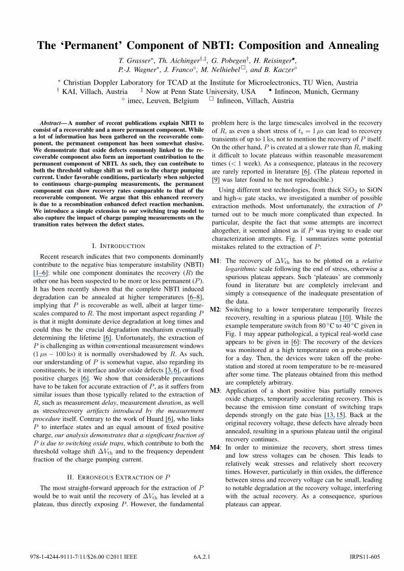
Using different test technologies, from thick SiO2 to SiONand high-κ gate stacks, we investigated a number of possibleextraction methods. Most unfortunately, the extraction of Pturned out to be much more complicated than expected. Inparticular, despite the fact that some attempts are incorrectaltogether, it seemed almost as if P was trying to evade ourcharacterization attempts. Fig. 1 summarizes some potentialmistakes related to the extraction of P :
M1: The recovery of ΔVth has to be plotted on a relativelogarithmic scale following the end of stress, otherwise aspurious plateau appears. Such ‘plateaus’ are commonlyfound in literature but are completely irrelevant andsimply a consequence of the inadequate presentation ofthe data.
M2: Switching to a lower temperature temporarily freezesrecovery, resulting in a spurious plateau [10]. While theexample temperature switch from 80 ◦C to 40 ◦C given inFig. 1 may appear pathological, a typical real-world caseappears to be given in [6]: The recovery of the deviceswas monitored at a high temperature on a probe-stationfor a day. Then, the devices were taken off the probe-station and stored at room temperature to be re-measuredafter some time. The plateaus obtained from this methodare completely arbitrary.
M3: Application of a short positive bias partially removesoxide charges, temporarily accelerating recovery. This isbecause the emission time constant of switching trapsdepends strongly on the gate bias [13, 15]. Back at theoriginal recovery voltage, these defects have already beenannealed, resulting in a spurious plateau until the originalrecovery continues.
M4: In order to minimize the recovery, short stress timesand low stress voltages can be chosen. This leads torelatively weak stresses and relatively short recoverytimes. However, particularly in thin oxides, the differencebetween stress and recovery voltage can be small, leadingto notable degradation at the recovery voltage, interferingwith the actual recovery. As a consequence, spuriousplateaus can appear.
978-1-4244-9111-7/11/$26.00 ©2011 IEEE 6A.2.1 IRPS11-605

10-4
10-2
100
102
104
106
108
0
10
20 -
ΔVth
[m
V]
10-6
10-3
100
103
106
Relaxation Time [s]
0
10
20
-ΔV
th [
mV
]
P?
Not P!
2.2nm PNO-2.2V/30
oC
Total Time
10-4
10-2
100
102
104
106
0
5
10
15
20
-ΔV
th [
mV
]
10-4
10-2
100
102
104
106
Relaxation Time [s]
0
5
10
15
20
-ΔV
th [
mV
]
80oC
40oC
P?
Not P!
30nm SiO21ks @ 6MV/cm/80
oC
Switch to Lower T
10-4
10-2
100
102
104
106
20
25
30
35
-ΔV
th [
mV
]
10-4
10-2
100
102
104
106
Relaxation Time [s]
20
25
30
35
-ΔV
th [
mV
]
P?
Not P!
30nm SiO2
Short Discharge Bias
1ks @ 6MV/cm125
oC
10-4
10-2
100
102
104
106
0
2
4
6
8
-ΔV
th [
mV
]
10-4
10-2
100
102
104
106
Relaxation Time [s]
0
2
4
6
8
-ΔV
th [
mV
]
RelaxUnstressed
P?
Not P!
1.4nm PNO
Higher Readout Voltage
Vs = -1.2VVr = -0.5VVth = -0.3V
125oC
10-2
100
102
104
106
0
100
200
300
400
ΔIC
P [
pA]
10-2
100
102
104
106
Relaxation Time [s]
0
100
200
300
400
ΔIC
P [
pA]
RelaxUnstressed
P?
Not P!
1.5nm High-κ
Large CP Range
Vs = -2.1VVH = -0.75VVL = +0.75VVth = -0.3V
M1 M2 M3 M4 M5
Fig. 1. Potential mistakes encountered while trying to locate plateaus in ΔVth recovery traces. The top figures show apparent plateaus, which have nothingto do with permanent degradation. The reasons for the occurrence of these plateaus are illustrated in the bottom figures. From left to right: (M1) The recoveryof ΔVth is plotted as a function of the total time, rather than the recovery time tr. Even if the recovery perfectly follows log(tr), a spurious plateau willappear if the data is plotted this way, which has nothing whatsoever to do with P . Similar considerations relate to plotting the data on a linear scale, wherethe spurious plateau depends solely on the measurement time. (M2) Due to the large recovery time required, the device is only kept at stress temperaturefor a short amount of time [6] and, to ease measurement, recovery is continued at a lower temperature. This, however, is pointless, as a switch to a lowertemperature freezes the recovery [10], which results in a spurious plateau. (M3) In order to remove R, which is due to trapped holes in the oxide [6, 11–13],a positive bias could be applied [14]. However, since the trap sites are switching traps, this has basically the same effect as a temperature switch, becausesuch a bias switch only removes a few decades from the recovery trace, which continues after that. (M4) Relaxation gate voltages only slightly larger than thethreshold voltage can already lead to degradation, in this example Vrelax = −0.5 V, with Vth = −0.3 V. As a result, degradation overlaps with the ‘normal’recovery, resulting in a spurious plateau for a certain amount of time. The signature of this plateau is that it disappears when either stress or relaxation voltagesare changed. (M5) If the charge pumping amplitude is chosen too large, for this 1.5 nm high-κ device for example from ±0.75 V, degradation is observedduring the CP measurement, again resulting in a spurious plateau as in (M4). Note the strong relaxation of ΔICP, which is anything but constant.
M5: Similarly to M4, charge pumping (CP) measurements canlead to degradation of ΔICP when the charge pumpingamplitude is chosen too large. Balancing the recoveryof ΔICP, this can lead to spurious plateaus as well,just like M4. M5 already highlights an important issue[16]: ΔICP is not constant, even within conventionalmeasurement windows, contradicting claims that ΔICP
is nearly constant and equal to P [1, 6]. In particular, theresemblance between the recovery of ΔVth in M4 andΔICP in M5 is indeed striking.
III. ATTEMPTS AT EXTRACTING P
We proceed by analyzing ΔVth recovery traces recorded af-ter carefully selected stress/recovery voltages, stress/recoverytimes, and temperature. A typical plateau at the end of therecovery is shown in Fig. 2. According to Huard [6], thisplateau is due to semi-permanent interface states ΔNit andfixed oxide charges. Interface states are fast and can quicklyfollow changes in the bias (< 1ms). Thus, a change of theinterfacial Fermi-level would result in a rapid change of thecharge stored in these interface states, ΔQit(EF), accordingto their density-of-states. In particular, after a temporary biaschange, the same ΔVth would be expected back at the originalbias. This is clearly not the case. In fact, ΔVth only slowlygoes back to its original value, an apparent degradation duringthe recovery phase [14]. We call this phenomenon reverserecovery, which thus indicates that a significant part of Pis due to slow oxide defects, ΔNot, such as those observedpreviously [11, 13, 17]. The explanation of the reverse recoveryeffect is as follows: during stress, defects are created insidethe oxide. These defects have an energy level in the silicon
10-6
10-4
10-2
100
102
104
106
Relaxation Time [s]
0
5
10
15
20
25
30
-ΔV
th [
mV
]
Ref1ms10ms100ms1s10s
10-6
10-4
10-2
100
102
104
Relaxation Time [s]
1s @ +1V➡
~40% ReverseRecovery
2.2nm PNO10s @ -2.3V/175
oC
Fig. 2. Typical plateau observed under medium stress conditions. After theplateau has been reached, a positive bias was applied for a short time. ForP ∼ ΔNit, one would expect ΔVth to rapidly follow bias changes (within a1 ms). In fact, a pronounced reverse recovery is observed with time constantsas large as 10 ks, indicating that ΔNot contributes to P .
bandgap and their occupancy depends on the position ofthe Fermi-level. During application of a positive bias, thedefects are discharged. This does not mean that the defectsare annealed, the discharging step just makes them electricallyneutral and thus invisible in ΔVth. Once in this metastableneutral state, the defects can either completely anneal orthey can be charged again when the Fermi-level is movedback to the threshold voltage. However, as the time constantsresponsible for charging and discharging can be considerably
6A.2.2IRPS11-606
10-6
10-4
10-2
100
102
104
Relaxation Time [s]
0
5
10
15
20
25
30 -
ΔVth
[m
V]
-2.3V -2.1V -1.9V
10-6
10-4
10-2
100
102
104
Relaxation Time [s]
1s @ +1V➡
2.2nm PNO10s @ 175
oC
Reverse Recovery
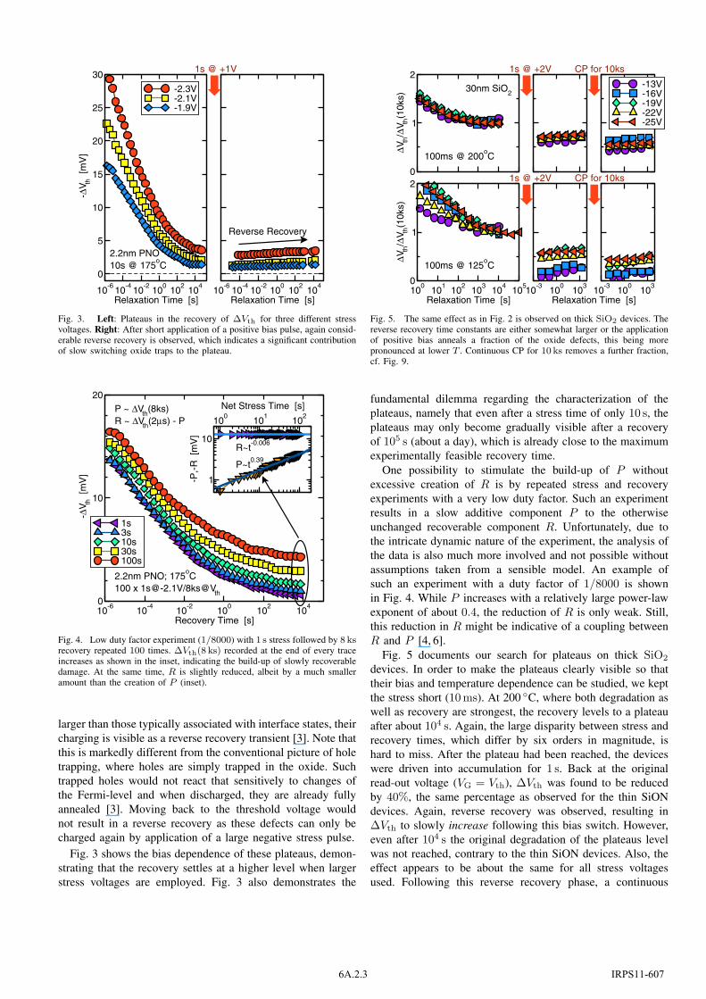
Fig. 3. Left: Plateaus in the recovery of ΔVth for three different stressvoltages. Right: After short application of a positive bias pulse, again consid-erable reverse recovery is observed, which indicates a significant contributionof slow switching oxide traps to the plateau.
10-6
10-4
10-2
100
102
104
Recovery Time [s]
0
10
20
-ΔV
th [
mV
]
1s3s10s30s100s
100
101
102
Net Stress Time [s]
1
10
-P,-
R [
mV
]
P~t0.39
R~t-0.006
2.2nm PNO; 175oC
100 x [email protected]/8ks@Vth
P ~ ΔVth(8ks)R ~ ΔVth(2μs) - P
Fig. 4. Low duty factor experiment (1/8000) with 1 s stress followed by 8 ksrecovery repeated 100 times. ΔVth(8 ks) recorded at the end of every traceincreases as shown in the inset, indicating the build-up of slowly recoverabledamage. At the same time, R is slightly reduced, albeit by a much smalleramount than the creation of P (inset).
larger than those typically associated with interface states, theircharging is visible as a reverse recovery transient [3]. Note thatthis is markedly different from the conventional picture of holetrapping, where holes are simply trapped in the oxide. Suchtrapped holes would not react that sensitively to changes ofthe Fermi-level and when discharged, they are already fullyannealed [3]. Moving back to the threshold voltage wouldnot result in a reverse recovery as these defects can only becharged again by application of a large negative stress pulse.
Fig. 3 shows the bias dependence of these plateaus, demon-strating that the recovery settles at a higher level when largerstress voltages are employed. Fig. 3 also demonstrates the
100
101
102
103
104
105
Relaxation Time [s]
0
1
2
ΔVth
/ΔV th
(10k
s)
10-3
100
103
Relaxation Time [s]10
-310
010
3
0
1
2
ΔVth
/ΔV th
(10k
s)
-13V -16V -19V -22V -25V
1s @ +2V➡1s @ +2V➡
CP for 10ks➡
CP for 10ks➡30nm SiO2
100ms @ 200oC
100ms @ 125oC
Fig. 5. The same effect as in Fig. 2 is observed on thick SiO2 devices. Thereverse recovery time constants are either somewhat larger or the applicationof positive bias anneals a fraction of the oxide defects, this being morepronounced at lower T . Continuous CP for 10 ks removes a further fraction,cf. Fig. 9.
fundamental dilemma regarding the characterization of theplateaus, namely that even after a stress time of only 10 s, theplateaus may only become gradually visible after a recoveryof 105 s (about a day), which is already close to the maximumexperimentally feasible recovery time.
One possibility to stimulate the build-up of P withoutexcessive creation of R is by repeated stress and recoveryexperiments with a very low duty factor. Such an experimentresults in a slow additive component P to the otherwiseunchanged recoverable component R. Unfortunately, due tothe intricate dynamic nature of the experiment, the analysis ofthe data is also much more involved and not possible withoutassumptions taken from a sensible model. An example ofsuch an experiment with a duty factor of 1/8000 is shownin Fig. 4. While P increases with a relatively large power-lawexponent of about 0.4, the reduction of R is only weak. Still,this reduction in R might be indicative of a coupling betweenR and P [4, 6].
Fig. 5 documents our search for plateaus on thick SiO2
devices. In order to make the plateaus clearly visible so thattheir bias and temperature dependence can be studied, we keptthe stress short (10ms). At 200 ◦C, where both degradation aswell as recovery are strongest, the recovery levels to a plateauafter about 104 s. Again, the large disparity between stress andrecovery times, which differ by six orders in magnitude, ishard to miss. After the plateau had been reached, the deviceswere driven into accumulation for 1 s. Back at the originalread-out voltage (VG = Vth), ΔVth was found to be reducedby 40%, the same percentage as observed for the thin SiONdevices. Again, reverse recovery was observed, resulting inΔVth to slowly increase following this bias switch. However,even after 104 s the original degradation of the plateaus levelwas not reached, contrary to the thin SiON devices. Also, theeffect appears to be about the same for all stress voltagesused. Following this reverse recovery phase, a continuous
6A.2.3 IRPS11-607

10-6
10-5
10-4
10-3
10-2
10-1
100
101
102
Relaxation Time [s]
0
2
4
6
8 -
ΔVth
[m
V]
-1.8V -2.0V -2.2V -2.4V -2.6V -2.8V
1.8nm PNO100μs @ 150
oC
Fig. 6. Plateaus are occasionally also observed after ultra-short stress times,shown for a 1.8 nm PNO device. The plateaus are not permanent and stronglydepend on the stress bias. Particularly after such weak stresses, it is importantthat the degradation at VG = Vth is negligible in order to avoid mistake M4of Fig. 1.
CP measurement lasting 104 s was performed. At the endof this CP measurement, the degradation level was reducedby about 60% relative to the original plateau value. Again,even after such a long CP measurement, reverse recovery wasvisible. The same experiment was repeated at 125 ◦C where theplateaus were only reached after a considerably longer time.Now, the response of the devices to the short accumulationpulse and the long charge pumping measurement dependedon the stress voltage used.
IV. BIAS DEPENDENCE OF P
For lifetime back-extrapolation, the bias dependence of Pis crucial. This is mostly due to the fact that at higher stressvoltages and temperatures, the contribution of P relative toR apparently increases, which has to be corrected for whenextrapolating back to operating conditions. Huard [6] observedP ∼ Eγ
ox with a technology-independent γ = 4, withoutgiving details of the extraction scheme for P .
Another example showing experimentally observableplateaus which appear already after a ts = 100μs stress isgiven in Fig. 6. The Eox dependence of these plateaus is shownin Fig. 7, together with the plateaus of Figs. 3–5 and relatedexperiments. Contrary to the universal exponent of 4 givenby Huard, a wider range is observed, with values smaller andlarger than 4. Also, the bias dependence of the plateaus inthe thick SiO2 devices (Fig. 5) shows exponents around 3.2at 200 ◦C and in the range 4.2–5.6 at 125 ◦C. The latter isinsofar interesting as the initial plateau has γ = 4.2, whichincreases to 5.2 after application of +2V for 1 s, and even to5.6 after continuous CP measurements for 10 ks. This againdemonstrates that P , whatever it is and by whatever means itis extracted, is not really permanent.
10-3
10-2
10-1
100
101
102
103
ΔIC
P [
nA]
10Electric Field [MV/cm]
10-3
10-2
10-1
100
101
102
103
-ΔV
th [
mV
]
PlateauPost 1s@+2VPost 10ks CP2.2nm PNO1.8nm PNO
3nm SiO2ts=100s
200oC
175oC
150oC
125oC
2.84.13.34.0
10 x
4.24.34.95.47.0
CP-Delay41ms;100ms;1s;10s;100s
1.5nm High-κ100s@125
oC
30nm SiO2ts=100ms
200oC
125oC
~3.24.25.25.8
4
6.1
100μs@150o C
10s
3 6
Fig. 7. The field dependence of the ‘permanent’ part. For the 1.8 nm PNOdevice from Fig. 6 we take P ∼ ΔVth(tr = 1 s), for the ones of Figs. 3and 5 P ∼ ΔVth(tr = 10 ks) was chosen. In addition, for the thick SiO2
devices, the last value at the end of the second and third relaxation cycle areshown (10 ks after the bias switch and 10 ks after the 10 ks CP measurementcycles). Also shown is the field dependence of the CP current, which appearsto behave in a similar manner. In any case, P can be fitted by a power-law∼ Eγ
ox.
10-3
10-2
10-1
100
ΔIC
P [
nA]
41ms100ms 1s 10s100s~E
γ
10-2
100
102
Duration
4
6
8
Exp
onen
t γ
1.5nm High-κ100s @ 125
oC
2 5 7Electric Field [MV/cm]
Fig. 8. The permanent component has been suggested to correlate withthe change in the charge pumping current, P ∼ ΔICP. Just like in ΔVth
measurements, the CP current is very sensitive to the measurement time inall our investigated technologies. This has a profound impact on the extractedbias dependence of P . Only for short CP measurements an E4
ox dependenceas in [6] is obtained.
V. CORRELATION WITH CHARGE-PUMPING DATA
It has been occasionally suggested [6, 19] that P is corre-lated to the CP current, ΔICP. In that context, ΔICP has beeninterpreted as being proportional to the number of interfacestates. Particularly at lower frequencies it has been observed,however, that ICP also contains considerable contributionsfrom oxide traps [20]. This issue has been commonly neglectedin the context of NBTI [21].
6A.2.4IRPS11-608

10-2
10-1
100
101
102
103
104
Recovery Time [s]
0
200
400
600
800
ΔIC
P [
pA]
Wait @ -2VWait @ +2VContinuous CP
0 0.5 1 1.5 2 -VH [V]
0
0.5
1
I CP [
nA]
ICP PreICP Post
6MV/cm @ 125oC
30nm SiO2
10-2
10-1
100
101
102
103
104
105
106
Recovery Time [s]
0
500
1000
1500
ΔIC
P [
pA]
Wait @ -0.5VWait @ +0.5VInterrupted @ -0.5VInterrupted @ +0.5VContinuous CP
1.5nm High-κ125
oC
Fig. 9. Recovery of the CP current at a frequency of 1 MHz. Contrary to otherobservations [6], the CP current is never constant in any of our technologies,consistent with [16]. Most importantly, continuous CP accelerates recovery.When the beginning of the CP measurement is delayed for variable amountsof time, with VG being either the CP high- or low-level, rapid recoveryis observed at the beginning of the delayed continuous CP measurement.Application of the CP high- and low-levels during the wait phase proves thatit is not the voltage but rather the charge pumping itself that causes the rapidrecovery. Top: For a thick 30 nm SiO2 device. The inset shows a constant-base-level CP sweep before and after stress. Bottom: For a 1.5 nm high-κgate stack device. The same effect is observed in both dramatically differenttechnologies.
The bias dependence of ΔICP is compared in Fig. 7 to thebias dependence of the ΔVth plateaus, which particularly forfast CP measurements seems to agree well, indicating a cor-relation between the defects visible in these two experiments.Such a correlation has led previous studies to conclude thatΔVth as well as ΔICP are dominated by interface states [22].
Interestingly, the bias dependence of ΔICP is very sensitiveto the measurement duration as shown in Fig. 8. While for fastCP experiments (41ms) we obtain γ = 4, we observe a strongdependence of the extracted exponent on the duration of theCP measurement. This is reminiscent to ΔVth measurements[23], where the exponent also increases with the measurementduration. The reason for this behavior is that ΔICP shows
10-3
10-2
10-1
100
101
102
103
104
Recovery Time [s]
0
0.2
0.4
0.6
0.8
1
1.2
1.4
Nor
mal
ized
ΔI C
P a
nd Δ
V th
Delay 1sDelay 10sDelay 100sDelay 1000sContinuous CPΔVthΔVth Post 1ks CP
CP Delayed @ VH (-0.5V)Readout ΔIS→ΔVth During Delay
1.5nm High-κ125
oC
ΔVth Post 1ks CP
Fig. 10. Extension of the experiment in Fig. 9: the change in the linearsource current ΔIS at the CP high-level VH is read during the wait phase andconverted to ΔVth following [18]. This clearly demonstrates that the onsetof the accelerated CP recovery follows the recovery of ΔVth. CP inducedaccelerated recovery in ΔICP is paralleled by a recovery in ΔVth by thesame fraction.
10-2
10-1
100
101
102
103
104
105
106
107
Relaxation Time [s]
0
1
2
3
4
5ΔN
eff [
1011
cm
-2]
Fit: A tr-n
1kHz10kHz100kHz1MHz2.5MHz
0 0.5 -VH [V]
02468
10
N eff [
1010
cm
-2]
UnstressedVL = +0.5V
1.5nm High-κ125
oC
Fig. 11. Frequency dependence of the CP recovery. With lower frequency, alarger amount of oxide defects contributes to ΔNeff . With increasing CPtime, however, the oxide defects are ‘pumped-away’, giving a frequencyindependent ΔNeff as expected from a pure ΔNit contribution.
similar recovery rates as ΔVth which is contrary to Huard’swork, but consistent with the observation of Rangan et al. [16].
Remarkably, recovery is accelerated by the CP measure-ment, see Fig. 9. The effect is quite similar for thick SiO2
and thin high-κ devices. At first glance one might relate thisto the bias-dependence of the defect annealing rates, since thetransistor is continuously pulsed between accumulation andinversion. As it has already been shown for ΔVth recovery,recovery can be accelerated when the transistor is driventowards accumulation [3, 23]. This effect, so undoubtedlypresent, does not provide the full answer, though. This can beseen in Fig. 9 which also shows reference CP measurementswhich were interrupted by constant bias phases at the low-
6A.2.5 IRPS11-609

10-2
10-1
100
101
102
103
104
105
Recovery Time [s]
0
20
40
60
80
100 -
ΔVth
[m
V]
10-2
10-1
100
101
102
103
104
105
Time After End of CP [s]
0
1
2
3
|ΔV th
- Δ
V th(1
0ms)
|
0s Ref1s10s100s1ks10ks
Reduced Reverse Recovery
1.5nm High-κ125
oC
CP Followed by ΔVth Meas.
Cont. CP
Fig. 12. Impact of continuous CP measurements with variable duration onΔVth. A considerable recovery in ΔVth is observed. Also, with increasingCP duration, the reverse recovery is reduced, indicating that CP anneals slowoxide defects, ΔNot.
and high-level of the charge pumping pulse, which accordingto the previous argument should contain the most effectiverecovery case. However, the ΔICP recovery in the continuousCP measurement is even larger, implying that it is acceleratedby the pulsing event itself.
Fig. 10 shows that ΔICP at the beginning of delayed CPmeasurements follows the recovery of ΔVth. Also, the amountof recovery induced by the CP measurement is mirroredin the recovery of ΔVth. This data strongly suggests thatboth ΔVth and ΔICP are at least partially related to thesame microscopic defect, namely switching oxide traps [13,24–26]. This conclusion is also confirmed by the frequencydependence of the ΔICP recovery shown in Fig. 11 whichgradually becomes smaller after long CP times, indicating thatit is oxide defects which can be ‘pumped-away’.
Further confirmation that defects visible in ΔVth react to CPmeasurements is given in Fig. 12: following a CP cycle, ΔVth
shows reverse recovery due to slow oxide defects reachingtheir equilibrium occupancy after long times. Since this reverserecovery becomes smaller and smaller with increasing recov-ery time, it must be concluded that the defects responsible forreverse recovery can recover as well.
In [27] it was argued that the recovery of ICP was not dueto the actual recovery of interface states, but rather due toa reduction of the swing of the surface potential. Althoughwe fail to see why the ‘width of the CP hat’ should berelated to the density of interface states, we performed fullconstant amplitude and constant-base-level CP measurementsin addition to the single-point CP experiments shown in theprevious figures. The result is shown in Fig. 13 and quitereassuringly, the same level of degradation and recovery isobserved in all measurements, except for the 1V constantamplitude CP measurements, which use an amplitude too smallto cover the whole bandgap. Fig. 13 also shows the detrimentalimpact of CP measurements which can lead to degradationand thus to artificial plateaus, cf. (M5), particularly at highertemperatures.
10-2
10-1
100
101
102
103
104
105
106
Time [s]
1
10
100
ΔIC
P [
%]
SinglePoint ±0.75CBL -0.75VCA ΔV=1.5VCA ΔV=1.0V
1.5nm High-κ50
oC
CP Caused DegradationUnstressed Devices
125oC
SinglePoint ±0.75
CBL -0.75V
CA ΔV=-0.75V
Fig. 13. All CP methods see the same recovery rate (ΔICP/decade), plottedrelative to ICP,0. The single-point CP method is the fastest and gives thesame ΔICP as the full constant-base-level sweep (CBL). Comparable fullconstant-amplitude (CA) sweeps with proper ΔV also see the same ΔICP.Particularly at higher temperatures, CP measurements can lead to degradation.
RelaxationStructural
RelaxationStructural
2’
PositiveMetastable
Substratewith
ExchangeCharge
NeutralStable 2
PositiveStable1
1’
Substratewith
ExchangeCharge
MetastableNeutral
FastSlow
Defect Annealing Charge Changes
SlowReverse RecoveryCharge Pumping
Distributed TimeconstantsDistributed Timeconstants
Fast
Fast Slow
Distributed Timeconstants
Defect Creation
+
+
+
Fig. 14. The switching oxide trap model developed recently [13] is consistentwith the experimentally observed behavior. Created defects can be switchingtraps and exchange charge with the substrate (1′ ↔ 2), some of them faster,contributing to ΔICP in a frequency-dependent manner, some of them veryslow, thus causing reverse recovery or transient RTN [13], thereby contributingto ΔVth only (if in state 2).
VI. THE DEFECT MODEL
Except for the newly discovered effect of CP-induced recov-ery, which will be discussed separately below, all features ob-served so far are consistent with the detailed defect propertiesidentified using our recent time-dependent defect spectroscopy(TDDS) measurements [13, 15]. The microscopic model weuse for the description of the defects is an extension of theswitching trap model proposed by Lelis et al. [24] and shownin Fig. 14:
• The defects are switching traps, that is, have an energy-level in the Si bandgap. Prior to stress, the defect is in theneutral state 1, while stress transfers it into the positivestate 2. Depending on the defect properties, the defect
6A.2.6IRPS11-610

1.5 2 2.5 3 3.5 4 4.5 5 5.51000/T [1/K]
ΔIC
P R
ecov
ery
[%]
Wait @ -0.5VWait @ +0.5VContinuous CP ±0.5V 13 meV
8 meV
1 meV
1.5nm High-κ1ks @ -2.1V; 10ks Recovery
20
30
40
50
60
70
80
Fig. 15. Temperature dependence of the CP recovery: Continuous CPrecovers ΔICP down to 30% of the post-stress ΔICP, nearly independentlyof temperature. Remaining at −0.5 V maintains 60% at −60 ◦C. Mereapplication of +0.5 V, the worst-case in a bias-driven interpretation, reducesΔICP only down to 40% at −60 ◦C.
may have a neutral metastable state 1′, which provides theaforementioned energy-level in the bandgap. Transitionsfrom 2 to 1′ are particularly likely during switches towardaccumulation or during CP measurements. While in 1′,the defect is uncharged and thus not visible in ΔVth.
• The defects may contribute to the CP signal in two ways.First, on an unstressed device, transitions between 1 and2′, provided they are sufficiently fast, can create recombi-nation events. Contrary to interface states, whose contri-bution is temperature-independent, these switching trapswill provide a larger contribution at higher temperatures.In particular, they will form the temperature-dependenttail of constant-base-level CP measurements. In addition,as shown in Fig. 13, CP can lead to degradation, whichcorresponds to a transition to state 2. Once in state 2,transitions between 2 and 1′ can also contribute to ICP,resulting in a temperature- and bias-dependent hysteresisof the CP curve [21].
• During NBTI stress, the defects move from the neutralstate 1 to stable state 2. There, again, transitions between2 and 1′ can also contribute to ICP, resulting in atemperature- and frequency-dependent contribution. Thisappears to be a significant contribution to ΔICP followingNBTI stress.
• Since the time-constants are widely distributed, only thefaster transitions between 2 and 1′ can contributed toICP. As seen in Figs. 2, 3, 5, and 12, the slower statesconstitute the reverse recovery effect.
• The reason why these switching traps can contribute toboth ΔVth and ΔICP is simply because once created,these defects can be either positive (state 2) or neutral(state 1′), depending on the Fermi-level, the formercontributing to ΔVth. This Fermi-level dependent defectoccupancy also causes the change in the sub-thresholdslope reported after NBTI stress [28, 29].
Positive
Neutral
1’
1 1
Pumping
Tot
al E
nerg
y (V
ibro
nic
+ E
lect
roni
c)
Reaction Coordinate
Stress
Charge
’Phonon−Kick’
22’
Fig. 16. Schematic illustration of the REDR effect: Top: During stress,defects become positively charged. Middle: During CP, the neutral level israpidly moved up and down, causing frequent transitions. Bottom: The excessenergy of the recombination events is deposited into the accepting mode,which leads to a reduction of the activation energy, known as the ‘phonon-kick’ or REDR effect [30].
VII. UNDERSTANDING CP-INDUCED RECOVERY
In order to understand the CP-induced recovery, we firststudied its temperature dependence which is shown in Fig. 15.At all temperatures, wait phases at −0.5V show relativelyweak recovery but a relatively strong temperature dependence.Compared to wait phases at −0.5V, wait phases at +0.5Vresult in a stronger recovery but have a weaker temperaturedependence. Finally, continuous CP measurements without anintermediate wait phases accelerate recovery down to 30% ofthe stress level after 10 ks, nearly independent of temperature.
A possible explanation for this behavior is as follows: theCP measurement at Imax
CP is designed to maximize the numberof recombination events. Each event releases an energy of theorder of the silicon bandgap. With 106 cycles per second, thisaccumulates to an enormous amount of energy which has to bedissipated via phonons. In due course, reactions near the defectsite can be dramatically enhanced, a phenomenon known as the‘phonon-kick’, or more recently as recombination enhanceddefect reaction (REDR) [30, 31]. This is schematically shownin Fig. 16, where the REDR accelerates the transition fromthe neutral metastable state to the neutral equilibrium state.Following the arguments of Weeks et al. [31], the thermaltransition rate from state 1 to state 1′ of our switching trapmodel [13],
k1′1 = ν e−βε1′1 (1)
with ε1′1 as the thermal barrier separating the states 1′ and 1′,is replaced by k1′1 + k∗
1′1 with the enhanced rate
k∗1′1 = ν∗ e−β(ε1′1−ε∗), (2)
with β−1 = kBT . From our experimental data we extractε∗ ≈ 60meV and ν∗ = 2.5 × 10¹⁴ s−1, with the convincingcalibration result shown in Fig. 17. We remark that, as noted
6A.2.7 IRPS11-611

20
40
60
80
100
120ΔI
CP [
%]
10-2
100
102
104
20
40
60
80
100
ΔIC
P [
%]
10-2
100
102
104
Recovery Time [s]
Wait @ -0.5VWait @ +0.5VCont. CP ±0.5
125oC -60
oC
Filled Syms: ModelOpen Syms: Data
Last@1ks Last@1ks
Fig. 17. Consideration of REDR in our switching trap model [3, 13] allows toreproduce the experimental data very well. Top: Data from Fig. 15 at 125 ◦Cand −60 ◦C. Bottom: The last long recovery trace during continuous CP at125 ◦C and −60 ◦C. The scatter particularly in the initial data (up to 20%)makes the model calibration challenging.
previously for ΔVth recovery [11], temperature-activated mi-croscopic defect time constants again result in an apparenttemperature-independent macroscopic behavior.
VIII. SPECIAL CASE: HYDROGEN-RICH WAFER
The log-like recovery of ΔICP as for instance shown inFigs. 9 and 13 is clearly incompatible with the recoverypredicted by the reaction-diffusion (RD) model [32], (1 +√
ts/tr)−1, which does not depend on bias or temperature[33]. A peculiar exception has been observed on a hydrogen-rich 30 nm SiO2 split-wafer. Measuring ΔICP only once perdecade results in ΔICP ∼ const. By contrast, a continuous CPmeasurement produces recovery traces which bear a strikingresemblance to the RD prediction, particularly for ts = 10 ks,see Fig. 18. After studying different stress times, however, wefound the measured recovery to be practically independent ofthe stress-time, not scaling universally over ts/tr as expectedfrom RD theory [33]. Still, under continuous CP conditions,recovery could be a diffusion-limited process in this particularwafer. An intriguing feature is that after longer stress timesthe devices continue to degrade after the end of stress. This isconsistent with the idea that hydrogen is released during stresswhich then depassivates interface states and creates oxidedefects [34–37]. Otherwise, degradation after termination ofthe stress would not be possible. We remark that this is thestandard model of irradiation damage [38, 39].
IX. CONCLUSIONS
We have demonstrated that the plateaus occasionally ob-served in carefully tuned stress/recovery experiments consistof contributions from interface states as well as slower donor-like switching oxide traps. These plateaus are not permanentand normally not too well developed, making a precise def-inition and extraction difficult. In particular, the plateaus can
0
0.2
0.4
0.6
0.8
1
Nor
mal
ized
ΔI C
P Continuous CPPaused@-2VContinuous CPRD
10-4
10-2
100
102
104
106
108
1010
Relaxation Time [s]
0
0.2
0.4
0.6
0.8
1
Nor
mal
ized
ΔI C
P
Continuous CPPaused@-2VContinuous CPRD
Excessive H Concentration Wafer
125oC
100s @ 6MV/cm
10ks @ 6MV/cm
10-3
10-2
10-1
100
101
102
103
104
105
106
107
108
Recovery Time [s]
0
0.2
0.4
0.6
0.8
1
Nor
mal
ized
ΔI C
P
RD100s1ks10ks100ks
Continuous CP
6MV/cm @ 125oC
30nm SiO2
Excessive H Concentration Wafer
Post-StressDegradation
Fig. 18. Top: In an extremely H-rich wafer, recovery in ΔICP isbasically absent provided only occasional CP measurements are made. Adiffusion-limited recovery behavior seems to dominate for continuous CPmeasurements. Bottom: The recovery rate appears to be roughly independentof the stress time, meaning that the hydrogen profile is only weakly disturbedduring stress. With increasing stress, though, the initial degradation during therecovery phase can last for up to 10 s and amount to 20%. This is a degradationof ΔICP which was found in this hydrogen-rich wafer only and must not beconfused with the reverse recovery visible in ΔVth only, cf. Fig. 12.
be annealed by applying short positive bias pulses or, moreeffectively, by continuous CP measurements. Particularly thelatter provides an efficient means for annealing NBTI degra-dation, likely due to a recombination enhanced defect reactionmechanism. Under normal recovery conditions, the recoveryof ΔVth determines the starting level of ΔICP, which startsrecovering quickly once CP measurements are performed.The latter demonstrates that oxide defects contribute to bothΔVth and ΔICP. Overall, considering P as permanent willlead to serious errors, even within conventional measurementwindows. Finally, we have suggested a simple extension ofour switching trap model to also account for recombinationenhanced defect reaction (REDR) effects.
6A.2.8IRPS11-612

ACKNOWLEDGMENT
This work has received funding from the EC’s FP7 grantagreement n◦216436 (ATHENIS) and from the ENIAC MOD-ERN project n◦820379.
REFERENCES
[1] V. Huard, M. Denais, and C. Parthasarathy, “NBTI Degradation:From Physical Mechanisms to Modelling,” Microelectronics Reliability,vol. 46, no. 1, pp. 1–23, 2006.
[2] T. Grasser, B. Kaczer, P. Hehenberger, W. Goes, R. O’Connor,H. Reisinger, W. Gustin, and C. Schlunder, “Simultaneous Extrac-tion of Recoverable and Permanent Components Contributing to Bias-Temperature Instability,” in Proc. Intl.Electron Devices Meeting (IEDM),2007, pp. 801–804.
[3] T. Grasser, B. Kaczer, W. Goes, T. Aichinger, P. Hehenberger, andM. Nelhiebel, “A Two-Stage Model for Negative Bias TemperatureInstability,” in Proc. Intl.Rel.Phys.Symp. (IRPS), 2009, pp. 33–44.
[4] T. Grasser and B. Kaczer, “Evidence that Two Tightly Coupled Mech-anism are Responsible for Negative Bias Temperature Instability inOxynitride MOSFETs,” IEEE Trans.Electron Devices, vol. 56, no. 5,pp. 1056–1062, 2009.
[5] T. Aichinger, M. Nelhiebel, and T. Grasser, “A Combined Study of p-and n-Channel MOS Devices to Investigate the Energetic Distribution ofOxide Traps after NBTI,” IEEE Trans.Electron Devices, vol. 56, no. 12,pp. 3018–3026, 2009.
[6] V. Huard, “Two Independent Components Modeling for Negative BiasTemperature Instability,” in Proc. Intl.Rel.Phys.Symp. (IRPS), 2010, pp.33–42.
[7] A. Katsetos, “Negative Bias Temperature Instability (NBTI) Recoverywith Bake,” Microelectronics Reliability, vol. 48, no. 10, pp. 1655–1659,2008.
[8] C. Benard, G. Math, P. Fornara, J. Ogier, and D. Goguenheim, “Influenceof Various Process Steps on the Reliability of PMOSFETs Submittedto Negative Bias Temperature Instabilities,” Microelectronics Reliability,vol. 49, pp. 1008–1012, 2009.
[9] H. Reisinger, O. Blank, W. Heinrigs, W. Gustin, and C. Schlunder, “AComparison of Very Fast to Very Slow Components in Degradation andRecovery Due to NBTI and Bulk Hole Trapping to Existing PhysicalModels,” IEEE Trans.Dev.Mat.Rel., vol. 7, no. 1, pp. 119–129, 2007.
[10] T. Aichinger, M. Nelhiebel, and T. Grasser, “Unambiguous Identifica-tion of the NBTI Recovery Mechanism using Ultra-Fast TemperatureChanges,” in Proc. Intl.Rel.Phys.Symp. (IRPS), 2009, pp. 2–7.
[11] H. Reisinger, T. Grasser, W. Gustin, and C. Schlunder, “The StatisticalAnalysis of Individual Defects Constituting NBTI and its Implicationsfor Modeling DC- and AC-Stress,” in Proc. Intl.Rel.Phys.Symp. (IRPS),2010, pp. 7–15.
[12] B. Kaczer, T. Grasser, P. Roussel, J. Franco, R. Degraeve, L. Ragnarsson,E. Simoen, G. Groeseneken, and H. Reisinger, “Origin of NBTI Vari-ability in Deeply Scaled PFETs,” in Proc. Intl.Rel.Phys.Symp. (IRPS),2010, pp. 26–32.
[13] T. Grasser, H. Reisinger, P.-J. Wagner, W. Goes, F. Schanovsky, andB. Kaczer, “The Time Dependent Defect Spectroscopy (TDDS) Tech-nique for the Bias Temperature Instability,” in Proc. Intl.Rel.Phys.Symp.(IRPS), May 2010, pp. 16–25.
[14] T. Grasser, B. Kaczer, and W. Goes, “An Energy-Level Perspective ofBias Temperature Instability,” in Proc. Intl.Rel.Phys.Symp. (IRPS), 2008,pp. 28–38.
[15] T. Grasser, H. Reisinger, P.-J. Wagner, and B. Kaczer, “The TimeDependent Defect Spectroscopy for the Characterization of Border Trapsin Metal-Oxide-Semiconductor Transistors,” Physical Review B, vol. 82,no. 24, p. 245318, 2010.
[16] S. Rangan, N. Mielke, and E. Yeh, “Universal Recovery Behavior ofNegative Bias Temperature Instability,” in Proc. Intl.Electron DevicesMeeting (IEDM), 2003, pp. 341–344.
[17] T. Grasser, H. Reisinger, W. Goes, T. Aichinger, P. Hehenberger, P. Wag-ner, M. Nelhiebel, J. Franco, and B. Kaczer, “Switching Oxide Trapsas the Missing Link between Negative Bias Temperature Instabilityand Random Telegraph Noise,” in Proc. Intl.Electron Devices Meeting(IEDM), 2009, pp. 729–732.
[18] B. Kaczer, T. Grasser, P. Roussel, J. Martin-Martinez, R. O’Connor,B. O’Sullivan, and G. Groeseneken, “Ubiquitous Relaxation in BTIStressing-New Evaluation and Insights,” in Proc. Intl.Rel.Phys.Symp.(IRPS), 2008, pp. 20–27.
[19] T. Aichinger, S. Puchner, M. Nelhiebel, T. Grasser, and H. Hutter,“Impact of Hydrogen on Recoverable and Permanent Damage followingNegative Bias Temperature Stress,” in Proc. Intl.Rel.Phys.Symp. (IRPS),2010, pp. 1063–1068.
[20] R. Paulsen and M. White, “Theory and Application of Charge-Pumpingfor the Characterization of Si-SiO2 Interface and Near-Interface OxideTraps,” IEEE Trans.Electron Devices, vol. 41, no. 7, pp. 1213–1216,1994.
[21] P. Hehenberger, T. Aichinger, T. Grasser, W. Goes, O. Triebl, B. Kaczer,and M. Nelhiebel, “Do NBTI-Induced Interface States Show FastRecovery? A Study Using a Corrected On-The-Fly Charge-PumpingMeasurement Technique,” in Proc. Intl.Rel.Phys.Symp. (IRPS), 2009.
[22] S. Mahapatra, K. Ahmed, D. Varghese, A. E. Islam, G. Gupta, L. Mad-hav, D. Saha, and M. A. Alam, “On the Physical Mechanism of NBTI inSilicon Oxynitride p-MOSFETs: Can Differences in Insulator ProcessingConditions Resolve the Interface Trap Generation versus Hole TrappingControversy?” in Proc. Intl.Rel.Phys.Symp. (IRPS), 2007, pp. 1–9.
[23] B. Kaczer, V. Arkhipov, R. Degraeve, N. Collaert, G. Groeseneken,and M. Goodwin, “Disorder-Controlled-Kinetics Model for NegativeBias Temperature Instability and its Experimental Verification,” in Proc.Intl.Rel.Phys.Symp. (IRPS), 2005, pp. 381–387.
[24] A. Lelis and T. Oldham, “Time Dependence of Switching Oxide Traps,”IEEE Trans.Nucl.Sci., vol. 41, no. 6, pp. 1835–1843, Dec 1994.
[25] J. Conley Jr., P. Lenahan, A. Lelis, and T. Oldham, “Electron SpinResonance Evidence for the Structure of a Switching Oxide Trap: LongTerm Structural Change at Silicon Dangling Bond Sites in SiO2,”Appl.Phys.Lett., vol. 67, no. 15, pp. 2179–2181, 1995.
[26] J. Ryan, P. Lenahan, T. Grasser, and H. Enichlmair, “Recovery-FreeElectron Spin Resonance Observations of NBTI Degradation,” in Proc.Intl.Rel.Phys.Symp. (IRPS), 2010, pp. 43–49.
[27] M. Denais, V. Huard, C. Parthasarathy, G. Ribes, F. Perrier, D. Roy,and A. Bravaix, “Perspectives on NBTI in Advanced Technologies:Modelling & Characterization,” in Proc. ESSDERC, 2005, pp. 399–402.
[28] C. Schlunder, M. Hoffmann, R.-P. Vollertsen, G. Schindler, W. Heinrigs,W. Gustin, and H. Reisinger, “A Novel Multi-Point NBTI Characteri-zation Methodology Using Smart Intermediate Stress (SIS),” in Proc.Intl.Rel.Phys.Symp. (IRPS), May 2008, pp. 79–86.
[29] D. Brisbin and P. Chaparala, “The Effect of the Subthreshold SlopeDegradation on NBTI Device Characterization,” in Proc. Intl.IntegratedReliability Workshop, 2008, pp. 96–99.
[30] H. Sumi, “Dynamic Defect Reactions Induced by Multiphonon Nonra-diative Recombination of Injected Carriers at Deep Levels in Semicon-ductors,” Physical Review B, vol. 29, no. 8, pp. 4616–4630, 1984.
[31] J. Weeks, J. Tully, and L. Kimerling, “Theory of Recombination-Enhanced Defect Reactions in Semiconductors,” Physical Review B,vol. 12, no. 8, pp. 3286–3292, 1975.
[32] M. Alam, “A Critical Examination of the Mechanics of Dynamic NBTIfor pMOSFETs,” in Proc. Intl.Electron Devices Meeting (IEDM), 2003,pp. 345–348.
[33] T. Grasser, W. Goes, V. Sverdlov, and B. Kaczer, “The Universality ofNBTI Relaxation and its Implications for Modeling and Characteriza-tion,” in Proc. Intl.Rel.Phys.Symp. (IRPS), 2007, pp. 268–280.
[34] L. Tsetseris, X. Zhou, D. Fleetwood, R. Schrimpf, and S. Pan-telides, “Physical Mechanisms of Negative-Bias Temperature Instabil-ity,” Appl.Phys.Lett., vol. 86, no. 14, pp. 1–3, 2005.
[35] S. Volkos, E. Efthymiou, S. Bernardini, I. Hawkins, A. Peaker, andG. Petkos, “The Impact of Negative-Bias-Temperature-Instability on theCarrier Generation Lifetime of Metal-Oxynitride-Silicon Capacitors,”J.Appl.Phys., vol. 100, no. 12, pp. 124 103–1–124 103–9, 2006.
[36] M. Houssa, V. Afanas’ev, A. Stesmans, M. Aoulaiche, G. Groeseneken,and M. Heyns, “Insights on the Physical Mechanism behind Nega-tive Bias Temperature Instabilities,” Appl.Phys.Lett., vol. 90, no. 4, p.043505, 2007.
[37] D. Dankovic, I. Manic, V. Davidovic, S. Djoric-Veljkovic, S. Golubovic,and N. Stojadinovic, “Negative Bias Temperature Instability in n-Channel Power VDMOSFETs,” Microelectronics Reliability, vol. 48, pp.1313–1317, 2008.
[38] F. McLean, “A Framework for Understanding Radiation-Induced Inter-face States in SiO2 Structures,” IEEE Trans.Nucl.Sci., vol. 27, no. 6,pp. 1651–1657, Dec 1980.
[39] D. Brown and N. Saks, “Time Dependence of Radiation-Induced TrapFormation in Metal-Oxide-Semiconductor Devices as a Function ofOxide Thickness and Applied Field,” J.Appl.Phys., vol. 70, no. 7, pp.3734–3747, 1991.
6A.2.9 IRPS11-613