Determination of bound-electronic and free-carrier nonlinearities in ZnSe, GaAs, CdTe, and ZnTe
10
Vol. 9, No. 3/March 1992/J. Opt. Soc. Am. B 405 Determination of bound-electronic and free-carrier nonlinearities in ZnSe, GaAs, CdTe, and ZnTe A. A. Said, M. Sheik-Bahae, D. J. Hagan, T. H. Wei, J. Wang, J. Young,* and E. W Van Stryland Center for Research in Electro-Optics and Lasers, University of Central Florida, Orlando,Florida 32816 Received May 30, 1991; revised manuscript received August 30, 1991 We extend the application of the Z-scan experimental technique to determine free-carrier nonlinearities in the presence of bound electronic refraction and two-photon absorption. We employthis method, using picosecond pulses in CdTe, GaAs, and ZnTe at 1.06 m and in ZnSe at 1.06 and 0.53 Am, to measure the refractive-index change induced by two-photon-excited free carriers (coefficient ar,), the two-photon absorption coefficient 1, and the bound electronic nonlinear refractive index n 2 . The real and imaginary parts of the third-order susceptibility (i.e., n 2 and 13, respectively) are determined by Z scans with low inputs, and the refraction from carriers generated by two-photon absorption (an effecitve fifth-order nonlinearity) is determined from Z scans with higher input energies. We compare our experimental results with theoretical models and deduce that the three measured parameters are well predicted by simple two-band models. n 2 changes from positive to nega- tive as the photon energy approaches the band edge, in accordance with a recent theory of the dispersion of n 2 in solids based on Kramers-Kronig transformations [Phys. Rev. Lett. 65, 96 (1990); IEEE J. Quantum Elec- tron. 27, 1296 (1991)]. We find that the values of 0-r are in agreement with simple band-filling models. I. INTRODUCTION The nonlinear-optical properties of semiconducting mate- rials are being widely studied as potential components of various optical devices. Among the areas of interest are optical switching and optical limiting. Large nonlineari- ties in InSb,' GaAs, 2 and HgCdTe (Ref. 3) were observed and used in demonstrating all-optical switching at inci- dent photon energies nearly resonant with the energy gap of the material. Large carrier nonlinearities are also observed in the transparency region where the carrier- excitation mechanism is two-photon absorption 48 (2PA). In the studies reported in Refs. 4-8 beam-distortion measurements at high irradiance were used to determine the nonlinear refraction, which was attributed solely to the free charge carriers, and the nonlinear refraction that was due to the bound electrons (electronic Kerr effect) was assumed to be negligible. However, picosecond time- resolved degenerate four-wave mixing experiments at much lower irradiance levels performed on ZnSe and CdTe in the presence of 2PA showed a large and fast third-order nonlinearity in addition to the higher-order carrier non- linearity. 9 The 2PA-generated carrier refraction is an effective fifth-order process.' 0 In the study reported in Ref. 11, which used the sensi- tivity of the Z-scan method to monitor nonlinear refrac- tion at low irradiance levels, a third-order nonlinearity was observed in ZnSe. This nonlinearity was attributed to n 2 , the nonlinear refraction caused by bound electrons, as was explained theoretically in Ref. 12. At higher irra- diance levels the refraction caused by the 2PA-generated free charge carriers becomes significant. In this paper we use the Z-scan technique" " 3 with picosecond pulses at several irradiance levels to determine the free-carrier re- fraction , separately, in addition to the bound electronic n 2 and the 2PA coefficient ,, in four different semiconduc- tors: ZnSe at 1.06 and 0.532 ,um and CdTe, GaAs, and ZnTe at 1.06 Am. With these measurements we are able to predict the contribution from each nonlinearity, given the experimental parameters (irradiance, pulse width, spot size, etc.). For example, we find here that the contribu- tion of n 2 to the experiments of Refs. 4-7 was as large as 50% for the lowest inputs used in those measurements but rapidly decreased for higher inputs. In Section 2 we briefly describe the Z-scan technique and the analysis for determining nonlinear absorption and refraction. Experimental results are given in Section 3. In Section 4 our measured values of the free-carrier re- fraction are compared with various theoretical models. We also compare our measured 3 and n 2 values with theo- retical values. In Section 5 we describe a simple alter- native method for estimating the different orders of nonlinear refraction, and we compare the results of this method with the results obtained by numerically fitting the experimental data. 2. Z SCAN The Z-scan experimental arrangement is shown in Fig. 1. The transmittance of a focused Gaussian beam through an aperture in the far field is measured as a function of the sample position z with respect to the focal plane- hence the name Z scan. While the input energy is kept constant, the sample experiences a different incident field (amplitude and phase) at different z positions. Nonlinear refraction in the sample manifests itself as beam broaden- ing or narrowing in the far field, thus changing the frac- tion of light passing through the aperture as the sample position is changed. Therefore the aperture transmit- tance is a function of the sample position z. As is ex- plained in Ref. 13, the sign of the nonlinear refraction is readily obtained from a Z-scan signal. An increase in transmittance followed by a decrease in transmittance (peak-valley) denotes a negative nonlinear refraction, whereas a valley-peak configuration implies a positive nonlinearity. Removal of the aperture, i.e., collecting all 0740-3224/92/030405-10$05.00 C 1992 Optical Society of America Said et al.
Transcript of Determination of bound-electronic and free-carrier nonlinearities in ZnSe, GaAs, CdTe, and ZnTe
Vol. 9, No. 3/March 1992/J. Opt. Soc. Am. B 405
Determination of bound-electronic and free-carriernonlinearities in ZnSe, GaAs, CdTe, and ZnTe
A. A. Said, M. Sheik-Bahae, D. J. Hagan, T. H. Wei, J. Wang, J. Young,* and E. W Van Stryland
Center for Research in Electro-Optics and Lasers, University of Central Florida, Orlando, Florida 32816
Received May 30, 1991; revised manuscript received August 30, 1991
We extend the application of the Z-scan experimental technique to determine free-carrier nonlinearities in thepresence of bound electronic refraction and two-photon absorption. We employ this method, using picosecondpulses in CdTe, GaAs, and ZnTe at 1.06 m and in ZnSe at 1.06 and 0.53 Am, to measure the refractive-indexchange induced by two-photon-excited free carriers (coefficient ar,), the two-photon absorption coefficient 1,and the bound electronic nonlinear refractive index n2. The real and imaginary parts of the third-ordersusceptibility (i.e., n2 and 13, respectively) are determined by Z scans with low inputs, and the refraction fromcarriers generated by two-photon absorption (an effecitve fifth-order nonlinearity) is determined from Z scanswith higher input energies. We compare our experimental results with theoretical models and deduce that thethree measured parameters are well predicted by simple two-band models. n2 changes from positive to nega-tive as the photon energy approaches the band edge, in accordance with a recent theory of the dispersion of n2in solids based on Kramers-Kronig transformations [Phys. Rev. Lett. 65, 96 (1990); IEEE J. Quantum Elec-tron. 27, 1296 (1991)]. We find that the values of 0-r are in agreement with simple band-filling models.
I. INTRODUCTION
The nonlinear-optical properties of semiconducting mate-rials are being widely studied as potential components ofvarious optical devices. Among the areas of interest areoptical switching and optical limiting. Large nonlineari-ties in InSb,' GaAs,2 and HgCdTe (Ref. 3) were observedand used in demonstrating all-optical switching at inci-dent photon energies nearly resonant with the energy gapof the material. Large carrier nonlinearities are alsoobserved in the transparency region where the carrier-excitation mechanism is two-photon absorption4 8 (2PA).In the studies reported in Refs. 4-8 beam-distortionmeasurements at high irradiance were used to determinethe nonlinear refraction, which was attributed solely tothe free charge carriers, and the nonlinear refraction thatwas due to the bound electrons (electronic Kerr effect)was assumed to be negligible. However, picosecond time-resolved degenerate four-wave mixing experiments atmuch lower irradiance levels performed on ZnSe and CdTein the presence of 2PA showed a large and fast third-ordernonlinearity in addition to the higher-order carrier non-linearity. 9 The 2PA-generated carrier refraction is aneffective fifth-order process.'0
In the study reported in Ref. 11, which used the sensi-tivity of the Z-scan method to monitor nonlinear refrac-tion at low irradiance levels, a third-order nonlinearitywas observed in ZnSe. This nonlinearity was attributedto n2, the nonlinear refraction caused by bound electrons,as was explained theoretically in Ref. 12. At higher irra-diance levels the refraction caused by the 2PA-generatedfree charge carriers becomes significant. In this paperwe use the Z-scan technique" "3 with picosecond pulses atseveral irradiance levels to determine the free-carrier re-fraction , separately, in addition to the bound electronicn2 and the 2PA coefficient ,, in four different semiconduc-tors: ZnSe at 1.06 and 0.532 ,um and CdTe, GaAs, andZnTe at 1.06 Am. With these measurements we are able
to predict the contribution from each nonlinearity, giventhe experimental parameters (irradiance, pulse width, spotsize, etc.). For example, we find here that the contribu-tion of n2 to the experiments of Refs. 4-7 was as large as50% for the lowest inputs used in those measurements butrapidly decreased for higher inputs.
In Section 2 we briefly describe the Z-scan techniqueand the analysis for determining nonlinear absorption andrefraction. Experimental results are given in Section 3.In Section 4 our measured values of the free-carrier re-fraction are compared with various theoretical models.We also compare our measured 3 and n2 values with theo-retical values. In Section 5 we describe a simple alter-native method for estimating the different orders ofnonlinear refraction, and we compare the results of thismethod with the results obtained by numerically fittingthe experimental data.
2. Z SCANThe Z-scan experimental arrangement is shown in Fig. 1.The transmittance of a focused Gaussian beam throughan aperture in the far field is measured as a function ofthe sample position z with respect to the focal plane-hence the name Z scan. While the input energy is keptconstant, the sample experiences a different incident field(amplitude and phase) at different z positions. Nonlinearrefraction in the sample manifests itself as beam broaden-ing or narrowing in the far field, thus changing the frac-tion of light passing through the aperture as the sampleposition is changed. Therefore the aperture transmit-tance is a function of the sample position z. As is ex-plained in Ref. 13, the sign of the nonlinear refraction isreadily obtained from a Z-scan signal. An increase intransmittance followed by a decrease in transmittance(peak-valley) denotes a negative nonlinear refraction,whereas a valley-peak configuration implies a positivenonlinearity. Removal of the aperture, i.e., collecting all
0740-3224/92/030405-10$05.00 C 1992 Optical Society of America
Said et al.

406 J. Opt. Soc. Am. B/Vol. 9, No. 3/March 1992
SAMPLE APERTURE
I I ~ ~Id I
Fig. 1. Z-scan experimental setup. D2/D is measured as afunction of the sample position z. D1, D2, detectors.
the transmitted light on detector D2, which we refer to asan open-aperture Z scan, will result in a flat response fora purely refractive nonlinearity. However, if nonlinearabsorption is present, then the transmittance signal ap-pears as an inverted Lorentzian, which has a minimum atz = 0 (the sample at the focal plane), where the irradianceis maximum. Nonlinear absorption suppresses the peakand enhances the valley in a closed-aperture Z scan (i.e.,with the aperture in place), as is seen, for example, inFig 3(b) below.
In order to analyze the Z-scan data we need to calculatethe electric field at the aperture for any position z of thesample. This calculation can be performed by solving thenonlinear equations for propagation inside the sample andthen those for propagation of the field in free space fromthe exit surface of the sample to the aperture. If thesample length is less than the confocal beam parameter,and if the phase changes in the field caused by the non-linear interaction are not transformed into amplitudechanges within the sample, then the sample is consideredthin 4" 5 (external self-action). Considering a thin sampleand using the slowly varying envelope approximation, wecan separate the wave equation into an equation for thephase and an equation for the irradiance7 :
dAbdz = kAn, (1)
dI= _ (a + OX (2)dz'- , 0 J,
where An is the change in the index of refraction, k is themagnitude of the wave vector in free space, a0 is the resid-ual linear absorption, and z' is the propagation distancewithin the sample, which is to be distinguished from z, thesample position with respect to the focal plane.
In our experiments we used 30-40-ps pulses at irradi-ance levels below the critical value for free-carrier absorp-tion.6 "7 Therefore Eq. (2) does not include free-carrierabsorption. We verified that free-carrier absorption wasnegligible in our experiments by measuring the same 2PAcoefficient at several irradiance levels. On the otherhand, we find that the refraction arising from these freecarriers cannot be neglected.' 8 Thus An in Eq. (1) iswritten as
An = yI + N, (3)
where y is the nonlinear index that is due to the boundelectrons and is related to the usual nonlinear index n2through n2(esu) = (cno/40ir)y(m2/W), with c the speed oflight in meters per second and a, the change in the indexof refraction per unit photoexcited charge-carrier densityN. If 2PA is the only mechanism for generating carriers,
the carrier-generation rate is given by
dN I2
dt 2hco(4)
Here we neglect the loss of carriers through recombina-tion and diffusion because these processes occur on timescales longer than the picosecond pulses that we use inthe experiments. Thus the carrier nonlinearity [rNin Eq. (3)] is proportional to a temporal integral of 12, re-sulting in an effective fifth-order nonlinearity; this con-clusion is reached by the same reasoning that makesthe index change caused by single-photon-absorption-generated free carriers an effective third-order effect. 9
In the 2PA case this fifth-order nonlinearity is a sequen-tial Im[xy3 )] process (i.e., 2PA) followed by a Re[x()] process(i.e., a linear index change from the carriers). The exis-tence of two nonlinearities of different orders and differ-ent decay times was also observed by Canto-Said et al.9 forpicosecond degenerate four-wave mixing. The fast non-linearity has a third-order dependence on the incident ir-radiance [X(3 ) effect], whereas the carrier nonlinearity hasa fifth-order dependence. The degenerate four-wavemixing technique cannot identify the nature (refractive orabsorptive) or the sign of these nonlinearities. Also, fromexamination of the two terms on the right-hand side ofEq. (3), it is clear that the electronic Kerr effect (y) willbe dominant at low irradiance levels, whereas the free-carrier refraction (rN) will dominate at high irradiancelevels.
The irradiance at the exit surface of the sample is ob-tained from Eq. (2) as
I(L, r, t, ) =(0, r, t, z)exp(-aoL)I(L~r~t~z) - 1 + q(r, t,z)()
where q(r, t, z) = jI(0, r, t, z)Leff, Leff = [1 - exp(-aoL)]/ao,and z is again the sample position. Here the irradiancewithin the sample is quoted after Fresnel reflections aretaken into account. This irradiance is taken as a Gauss-ian in space and time, given by
0, r, t, Z) = Io exp[-2(r/wO) 2- (t/to)2 ]1 + (/zo) 2 (6)
with z0 = 7rwo2/A. Removing the aperture in Fig. 1 isanalogous to placing detector D2 at the exit surface of thesample. Such an open-aperture Z scan allows us to ignorethe phase changes, and Eq. (5) leads to the normalizedtransmittance as calculated in Ref. 11 after integrationover the spatially and temporally Gaussian pulse:
T(z) = 12q(0, z) ln[1 + q(O,O,z)exp(- 2 )]d. (7)
The only unknown parameter in Eq. (7) is , in q(0, 0, z),which implies that an open-aperture Z scan will give the2PA coefficient. Figure 2 shows a plot of T(0) as a func-tion of q(0, 0, 0) = fJIoLeff. This curve can be used in anopen-aperture Z-scan transmittance measurement todetermine jG directly. At still higher irradiance levelsfree-carrier absorption must be included in Eq. (2), andan open-aperture Z scan could also be used to determinethe free-carrier absorption. With known from low-irradiance open-aperture Z-scan data, high-irradiancedata will permit calculation of the free-carrier absorption
Said et al.
(5)

Vol. 9, No. 3/March 1992/J. Opt. Soc. Am. B 407
1.00C)
.4-)4 0.80
E 0.60
a)
50.40
0Z
0.20 , E ,0.0 2.0 4.0 6.0 8.0
fIOLeff
Fig. 2. Normalized transmittance for an open-aperture Z scanat z = 0 as a function of 3IoLeff = q(0,0, 0). From this curve 3can be determined without fitting the data.
cross section. However, as is mentioned above, all the ex-periments reported here are below the critical irradiancefor free-carrier absorption.
The total phase change AO experienced by the beam isobtained by integrating Eq. (1), using Eq. (3), to give'
AO(r,t, z) = ln[1 + q(r, t, z)] + r dt'F(t'),we 2hoG J_
where
F(t) = a ln[1 + q(r, t, z)] - q(, ) [1Leff
exp(-aoL) 11 + q(r, t, z)J
The field at the exit surface of the sample is completelydetermined by Eqs. (5) and (8) [i.e., E cc I'12 exp(iAo)],where the reflection losses are included. The field at theaperture is determined by the Huygens-Fresnel propaga-tion integral2 0 :
EaStXz) = iA(d - z) P A(d - z)
x J r'dr'E(L, r, t, z)exp[A(7-z)]
2wrrr'A(d -), (10)
where d is the distance between the aperture and the focalplane. The transmitted power through the aperture isgiven by
PT(Z, t) = cono7r-J IEa(r, t)l 2 rdr, (11)
and the normalized transmittance is
f PT(t)dtT(z, S) = , (12)
Sf Pi(t)dt
where Pi(t) = I(r = 0, t, z = 0) (rwo2 /2) is the input power.
Here S is the linear aperture transmittance given byS = 1 - exp(-2ra2/wa2), with r and wa being the aper-ture radius and the beam radius at the aperture in thelinear regime, respectively. Equation (7) is identical toEq. (12) for S = 1. Note that Eq. (12) includes the losses,if any, by 2PA as well as losses that are due to the aper-ture. In what follows we compare the numerical evalu-ation of Eqs. (7) (nonlinear absorption only) and Eq. (12)with the experimental results.
3. EXPERIMENTAL RESULTS
We performed Z-scan experiments on three II-VI semicon-ductors, ZnSe, CdTe, and ZnTe, and a III-V semiconductor,GaAs. ZnSe is a two-photon absorber at 532 nm, whereasthe other three samples are two-photon absorbers at1.06 m. We first discuss experiments with ZnSe at532 nm. In the following measurements the irradiancevalues were carefully determined. The pulse width wasmeasured by performing autocorrelation experiments andwas monitored for each laser firing as described in Ref. 7,and the beam radius was determined from several pinholebeam scans. Using the Z-scan property AZ,-, = 1.7zo, wedouble-checked the beam scan results by performingZ-scan experiments on CS2 (see Ref. 11). The energyvalues were measured by calibrating the reference detec-tor against a calibrated Gentec energy meter.
A. 0.532-.um ResultsWith 27-ps (FWHM) pulses at 532 nm from a frequency-doubled NdYAG laser we performed Z scans at differentinput energies on a 2.7-mm-thick polycrystalline sample ofZnSe grown by chemical-vapor deposition. The samplehas an energy gap of 2.67 eV.2' The beam was focused toa radius of w0 = 25 m. First an open-aperture Z scanwas performed at Io = 0.21 GW/cm2. All the experimen-tal irradiances reported here are those within the sample(i.e., Fresnel reflections are taken into account). InFig. 3(a) we plot the experimental data and the theoreticalfit obtained by setting = 5.8 + 1.2 cm/GW in Eq. (7).This is within 5% of the value of 5.5 cm/GW reported inRef. 7. The fitting uncertainties for this measurementand for the measurements listed below were ±10o, but theoverall experimental uncertainty is +20o, arising mainlyfrom uncertainties in the irradiance calibration. Withthe 40% aperture (S = 0.4) another Z scan was performedat the same irradiance. In this case the measurement issensitive to both nonlinear refraction and nonlinear ab-sorption. Experiments on ZnSe were conducted at irradi-ance levels from 0.21 to 2.4 GW/cm2. At the lowestirradiance we expect the change in the index of refractionto be due mostly to the third-order anharmonic motion ofthe bound electrons." With p = 5.8 cm/GW and neglect-ing free-carrier refraction (i.e., o-, = 0), we fitted the ex-perimentaldataofFig. 3(b),usingy = -6.8 x 10⁻¹⁴ cm 2/W(n2 = -4.4 x 10⁻¹¹ esu) in Eq. (12). The negative sign ofn2 can easily be deduced from the peak-valley feature ofthe Z-scan signal. Note that the minus was inadvertentlyomitted in Ref. 11. The same experiment was repeated atI = 2.4 GW/cm2. The free-carrier contribution to the re-fraction becomes significant at this irradiance level. Inall, 10 Z scans were performed (5 open aperture and5 closed). Using an iterative approach to best-fit all thedata, we found a better fit by modifying n2 from -4.4 x
Said et al.
408 J. Opt. Soc. Am. B/Vol. 9, No. 3/March 1992
1.04ZnSe
) -532 nm
1. oo
-. 009
0.92
0
i~0.92
1.04ZnSe
X -532 nm
41.)0WE * 00g o
E 0.86 -
0 0 / S-0.4
0.92 0 (b0
07 Z~~~~~~~~~
0.88-24 -18 -8 0 8 la 24 32
Z (mm)
Fig. 3. Normalized Z-scan data of a 2.7-mm ZnSe sample mea-sured with 27-ps (FWHM) pulses and A = 532 nm at low irradi-ance (Io = 0.21 GW/cM2 ). The solid curves are the theoreticalfits. (a) Open-aperture data (S = 1) were fitted with , =5.8 cm/GW. (b) 40%-aperture data were fitted with , =5.8 cm/GW and n2 = -4.4 x 10⁻¹S esu.
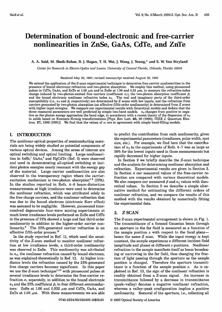
10-ll to -(4.0 0.8) 10-"l esu and using o- = -(0.8+0.2) 10`2l cm'. Thus there is a small contribution froma,, even at the lowest irradiance level. The data and fitfor Io = 0.57 and Io = 2.4 GW/cM2 are shown in Figs. 4(a)and 4(b), respectively. The agreement between experi-ment and theory is remarkable, given that the change intransmittance between the peak and the valley rangesfrom approximately 10% in Fig. 3(b) to 90% in Fig. 4(b).The absolute errors in the measurement of a, of 25% areonly slightly larger than those for ,B and , even though thenonlinearity is of a higher order. This result occurs inpart because the calculation of °r, depends on the products,BIo and yIo, which we know more accurately than ,l or yseparately.
B. 1.06-,u~m ResultsAll the Z-scan experiments discussed below were per-formed with 40-ps pulses (FWHM) from a Nd:YAG laserfocused to w 40 ,um. CdTe has an energy band gap of1.44 eV, which makes it a two-photon absorber at 1.06 ,um.The sample used is undoped, polycrystalline, and 3 mm
thick.2 ' Following the same procedure as for ZnSe, wewere able to determine ,B = 26 ± 5 cm/GW, as comparedwith 22 and 15 cm/GW for two different samples reportedin Ref. 7. We also found .y = -(3.0 ± 0.6) x 0-l' esu orn2 = -(2.0 ± 0.4) x 10-10 esu and ar = -(5.0 ± 1.2) x10-21 cm3 . The theoretical fit with Eq. (12) used for oneof the eight Z-scan experiments performed on CdTe withthe above values is shown in Fig. 5; the closed-aperturedata were taken at Io = 0.3 GW/cm2.
2PA and nonlinear refraction in GaAs were used for op-tical limiting in Ref. 18. However, the bound electronicand free-carrier refractive nonlinearities were not mea-sured separately. Recently high-irradiance measure-ments were used to estimate ar in GaAs while refractivecontributions from n 2 were ignored.2 2 We followed thesame steps taken in determining the nonlinearities forZnSe and CdTe, using data from eight Z scans. Figure 6shows the theoretical fit to the experimental data ex-tracted from a closed-aperture Z-scan experiment atIo = 0.45 GW/cm2 on a 1.2-mm-thick undoped single crys-
1.08
a)
r 1.00._I
Z 0.92
E
0 0.84N
Sco;., 0.760z
0.68
1.20
a)0
.. 0.900cn
-) 0.60
N
£ 030s-I
co
0z
0.00 -24 -16 -8 0 8 16 24 32
Z (mm)Fig. 4. Closed-aperture Z-scan data (S = 0.4) and theoreticalfits (solid curves) of the ZnSe sample taken at high irradiancelevels of (a) Io = 0.57 GW/cm2 and (b) Io = 2.4 GW/cm2 , wherefree-carrier refraction is significant. The data in (a) and (b) werefitted with ,B = 5.8 cm/GW, n2 = -4.0 x 10⁻¹ esu, and o, =-0.8 x 10⁻² cm3.
Said et al.

Vol. 9, No. 3/March 1992/J. Opt. Soc. Am. B 409
1.20 -
a 1.00
BEW 0.80
E
Q 0.60 N._2
O 0.40-0 "z
0.20 -
-50 -25 0 25 50
Z (mm)
Fig. 5. Closed-aperture Z-scan data (S = 0.4) for a 3-mm CdTesample with 1.06-btm, 40-ps (FWHM) pulses at Io = 300 MW/cm2 .The theoretical fit (solid curve) was obtained with 3 =26 cm/GW, n 2 = -2.0 x 10⁻¹C esu, and o = -5.0 x 10-
2 ' cm3
.
1.20 As
X= 1.06um *Q)
1.00
0.80
a 0.60
O' 0.40 E 0
0.20 l l-50 -25 0 25 50
Z (mm)
Fig. 6. Closed-aperture Z-scan data (S = 0.4) for a 1.2-mmGaAs sample with 1.06-Am, 40-ps (FWHM) pulses at Io =450 MW/cm2. The theoretical fit (solid curve) was obtained with. = 26 cm/GW, n2 = -2.7 x 10⁻¹⁰ esu, and or = -6.5 10-21 cm3 .
tal of GaAs of orientation (110) perpendicular to the sur-face.2' We saw no greater than a 10% anisotropy onchanging polarization in any of the nonlinear coefficients.We measured 13 = 26 + 5 cm/GW (23 cm/GW in Ref. 7and 26 cm/GW in Ref. 15), n2 = -(2.7 ± 0.5) x 10-10 esuand ar = -(6.5 ± 1.6) x 10-21 cm 3 .
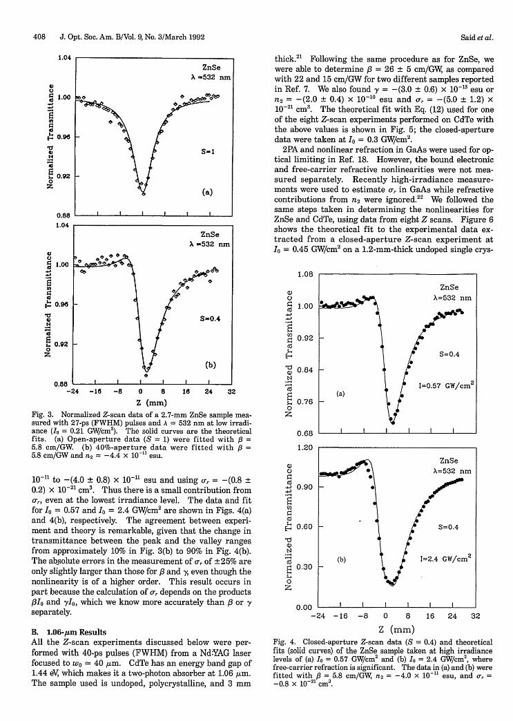
Z scans at 1.06 ,um were performed on a 2-mm-thicksingle crystal of ZnTe oriented with the (111) plane per-pendicular to the propagation direction.2 2 The shape ofthe Z-scan signal is drastically different from those of theother semiconductor materials. For example, a peak-valley or valley-peak signature is not obvious from thedata of Fig. 7. In the three materials mentioned above,the bound electronic nonlinearity was found to be nega-
tive. Thus the bound- and free-carrier refraction are ofthe same sign, and so they add. This explains why theZ-scan signal maintains its peak-valley feature at low[Fig. 3(b)] and high (Fig. 4) irradiance levels. For each ofthese semiconductors the incident photon energy wasbelow but close to the band edge (i.e., well above the 2PAedge). The band gap of ZnTe, 2.26 eV, is almost resonantwith the two-photon transition, 2.34 eV
1.1
X 1.0
E-0.
-
'C)N
So0z 0.8
0.7 L--50 -30 -10 10 30 - 50
Z (mm)
Fig. 7. Closed-aperture Z-scan data (S = 0.4) and theoretical fit(solid curve) of the ZnTe sample at Io = 1.4 GW/cm2. The datawere fitted with 6 = 4.2 cm/GW, n2 = +8.3 x 10⁻¹¹ esu, anda-,= 0.75 x 10⁻²¹ cm3 . No definite peak-valley or valley-peaksignature can be observed.
1.05
Q).
co
ES
-0'C)
.N
0z
1.00 _
0.95 -
0.90 1_
0.85 -
0.80-60.0 -40.0 -20.0 0.0 20.0 40.0 60.0
Z (mm)
Fig. 8. Closed-aperture Z-scan data (S = 0.4) and theoretical fit(solid curve) of the ZnTe sample at Io = 0.6 GW/cm2. The datawere fitted with the same parameters used in Fig. 7. Thevalley-peak configuration indicates that the positive bound elec-tronic Kerr effect is dominant at this irradiance level.
CdTe
X= 1.06/.tm
I I IXI I I
11Vs 0
004s [ , ZnTeX= 1.06un
0
I I I
Said et al.
m
410 J. Opt. Soc. Am. B/Vol. 9, No. 3/March 1992
1.20
0) O
0 ~~~~~~ 0C5 ~~ ~~~0
*0E-' 1.00 0 %0)~~~~~01AW
11=f I 0 003b~~~~
N
0 0.90
0z0.80
Fig. 9. CloEZnSe at 1.06of Z = 7rwo2it changes532 nm.
Using thfor which n:peak signalThe positivpectations,diance of Icnegative frnot dominadifferent siZ-scan datelevels becaiLAs in the cobtained fr(value is /3The data ir0.4) x 10-1:
o,, = - (0.7values are kbecause dat
We alsotwo-photon+(1.7 ± O..aperture (S0.53 Am, shnonlinear al
by division. In Ref. 11 we showed that dividing theclosed-aperture Z-scan data by the open-aperture dataapproximates the purely refractive Z scan (also seeSection 5). This observed dispersion in n2 is consistentwith the recent theory of Refs. 12 and 23 and is discussedfurther in Section 4.
4. COMPARISONS BETWEEN EXPERIMENTAND THEORY
;t so 0,In this section we compare our experimental results withthose of proposed theoretical models for the different non-
) _ .b linearities involved. First, our measured values of the* 2 0PA coefficients agree well with earlier reported val-
% 00 ues.7l" Van Stryland et al.7 give a detailed comparison oftheir experimental results with existing theoretical mod-els24'25 for 2PA; their results showed remarkably good
-8 -4 0 4 8 agreement with simple two-parabolic-band second-orderZ/zo perturbation theory. Listed in Table 1 are our experi-
;ed-aperture (S = 0.4) Z-scan experimental data of mental values of /3 compared with experimental and theo-Aum (filled circles) and 532 nm (open circles) in units retical values from Ref. 7. Also consistent with the/A. This figure clearly shows the dispersion in n2 as results of Ref. 7, the only significant deviation betweenits sign from positive at 1.06 jzm to negative at experiment and theory was for ZnTe, in which /3 is approxi-
mately four times larger than predicted by this simplemodel. However, in ZnTe two photons couple states only
e relatively low irradiance of Io = 0.6 GW/cm2, 3% above the gap, where exciton enhancement and impu-2 is expected to dominate, we observed a valley- rity effects may be expected to be important.2 6
, indicating a positive n2, as is shown in Fig. 8. The n2 values of our results are compared in Table 1e sign of n2 is consistent with theoretical ex- with those calculated from the theoretical model of Sheik-as is discussed in Section 4. At the input irra- Bahae et al.12
'23 This theory relates n2 to the nonlinear
= 1.4 GW/cm2 used for the data of Fig. 7, the absorption by using a nonlinear Kramers-Kronig trans-ee-carrier refraction becomes significant but formation in a relation similar to that between the linear.nt. At this irradiance the two effects with absorption and index of refraction. The nonlinear ab-gns compete to give the unusual shape of the sorption was calculated by using two parabolic bands andL. We were unable to go to higher irradiance includes contributions from 2PA as well as from electronicise of the low damage threshold of the sample. Raman and ac-Stark effects. References 12 and 23 alsoither semiconductors, the 2PA coefficient was show that n2 is inversely proportional to the fourth powerom open-aperture Z-scan data. The measured of the energy gap. The trend in n2 as a function of the= 4.2 ± 1.1 cm/GW (4.5 cm/GW in Ref. 7). ratio of photon energy to band-gap energy23 shows smalli Figs. 7 and 8 were fitted with y = +(1.2 ± positive values for small ratios; this function slowly risesIcm/W (n 2 = +(8.3 ± 2.5) x 10-il esu) and to a broad resonance peak at the 2PA edge and then de-5 ± 0.25) x 10-21 cm3. The errors in these creases, eventually becoming negative between the two-somewhat higher than for the other materials photon and single-photon absorption edges. Thus thea from only four Z scans could be used. change from negative values of n2 for semiconductors inmeasured n 2 in ZnSe at 1.06 m, where which two photons couple states well above the gap (i.e.,absorption is not present. We obtained n2 = ZnSe, GaAs, and CdTe) to a positive value for ZnTe, in3) x 10-1 esu. In Fig. 9 we plot closed- which two photons couple states only 3% above the gap, is= 0.4) Z scans obtained in ZnSe at 1.06 and expected. Also expected is the positive value of n2 in
owing the change in sign of n2. For Fig. 9 the ZnSe at 1.06 Aim, where 2PA is not energetically allowed.bsorption was removed from the 0.53-/gLm data The excellent agreement between the predicted and mea-
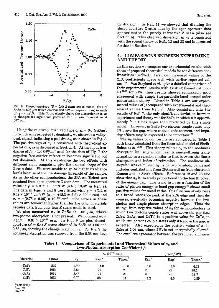
Table 1. Comparison of Experimental and Theoretical Values of n2 andTwo-Photon Absorption Coefficient 18
n 2 (10-11 esu) /3 (cm/GW)
Material A (nm) no Exp.a Theor.b Exp.' Exp.c Theor.c
ZnSe 532 2.70 -4.0 -3.8 5.8 5.5 4.27CdTe 1064 2.84 -20 -21 26 22 25.1GaAs 1064 3.43 -27 -31 26 23 19.7ZnTe 1064 2.79 83 54 4.2 4.5 0.89
aThis study.bRef 23.Ref 7.
- ZnSe
Said et al.

Vol. 9, No. 3/March 1992/J. Opt. Soc. Am. B 411
Table 2. Contributions to the Change in the Index of Refraction Caused by Plasma and Blockingfrom Various Interband Transitionsa
Blocking Blocking Blocking BlockingPlasma Electron Electron Plasma h-Hole Plasma 1-HoleElectron hh-c lh-c h-Hole hh-c 1-Hole lh-c
ZnSe 20% 33% 23% 4% 16% 2% 2%CdTe 27% 23% 21% 7% 15% 4% 3%GaAs 34% 25% 24% 3% 10% 2% 2%
a Here c, hh, and Ih refer to the conduction, heavy-hole, and light-hole bands, respectively.
sured n2 values, including the sign change, is seen fromTable 1.
We compare our results for the nonlinear refractioncaused by free carriers to two different band-filling mod-els (BF's). These models are the model attributed toAronov et al.2 7 and Auston et al.2 5 (BF1) and the dynamicMoss-Burstein model with Boltzmann statistics92930
(BF2). In these theories the change in refraction that isdue to carriers is independent of the means of carrier gen-eration. In BF1 the nonlinear refraction that is due tofree carriers is calculated directly from the real part ofthe complex dielectric function. The creation of N freeelectrons in the conduction band is accompanied by theelimination of N bound electrons in the valence band.For off-resonance excitation (ha) < Eg) the change in theindex of refraction is given by28
2VNe 2 Eg2
noi \M Eg 2_ (h=)2 (13)
where m,, is the reduced effective mass of the electrons inthe conduction band and the holes in the valence band.In Eq. (13) the hot-carrier effects were neglected becausethe carriers reach the band edge (thermal equilibriumwith the lattice) within 2 ps,28 which is short comparedwith our 27- and 40-ps pulses.
In BF2 the free carriers block the absorption at fre-quencies higher than the energy gap by filling the avail-able states in the conduction and the valence bands. Thismodel uses a Kramers-Kronig integral on this change inabsorption. The total change in the index of refraction,including contributions from electrons, heavy holes, andlight holes, is given by Wherrett et al. as 29
27-e2 A AN, [Z MMh mAn = - 2- + Z - Jh + Jlcnowo mc L m m
AP,1 + ZMJhh + ( )|
where
Z=4 mp2 (537i1/2 h2kB T (15)
x2 exp( - x2)= fx~e~(~x2 )dx, (16)f x 2 + aij '(6
Eg - h mcjaij = -. (17)
kB T mj
m is the electron mass, e is the electron charge, kB is theBoltzmann constant, T is the temperature in kelvins, P isthe Kane momentum3 ' given by E = 2P 2m/h 2, and E is
approximately 21 eV for semiconductors. AN and AP rep-resent the photogenerated electron and hole densities, andthe subscripts c, h, and represent the conduction, heavy-hole, and light-hole bands, respectively. i and j aredummy subscripts that represent c, h, or 1. APh and AP,are given by29
AN, 1 + (M)3/2APh Mh
AN I + (Mh)3/2AP, M
(18)
Equation (14) is an approximation that is adequate fornear-resonance radiation. Off resonance, as in 2PA, wefind that Jij should be replaced by Fij, where F is defined as
Fi = 2JQmc Eg ) + J(mci E- h)m kBT/ m; kB T/
+ J( mjEg+ h(19)
For hco Eg and Eg >> k T the first and third terms onthe right-hand side of Eq. (19) are extremely small com-pared with the second term; thus it is reasonable toneglect them, as was done in Eq. (14).929 In 2PA experi-ments Eg - h is comparable with Eg, and all three termsin Eq. (19) need to be retained.
The electrons' contribution to the index change is AN,of Eq. (14), and this term includes blocking caused by elec-tron transitions from the heavy-hole band and the light-hole band in addition to the change in the electronpopulation in the conduction band. APh and AP, give thecontributions of the holes. Table 2 lists the contributionof each of these effects for ZnSe, CdTe, and GaAs. In thecalculations for Table 2 Fij was used rather than Jii. It isseen from Table 2 that the change in the index of refrac-tion from transitions between the light-hole band and theconduction band (electron blocking, light-hole blocking,and free-light-hole generation) contributes =27% for allthree semiconductors listed. Thus it is reasonable to usethe approximation of a two-band model when only transi-tions from the heavy-hole band to the conduction band areconsidered. In our experiments the low-temperature con-dition, or hco - Egj >> k T is still satisfied; for example,in the worst case, that of GaAs, hc - Eg = 0.25 eV, andat room temperature kB T = 0.02 5 eV Examining Ji inEq. (16), we see for aij >> 1 that J'L = r"2/4a. Substitut-ing this value for Jj into Eq. (19), we find that Fij is propor-tional to x2/(1 - x2), where x = hcs/Eg. Assuming atwo-band model and substituting Fij for Jj in Eq. (14)shows that the change in the index of refraction that isdue to the carrier transition blocking is
An(blocking) x (hw)2/[Eg2 - (ho)2], (20)
Said et al.
412 J. Opt. Soc. Am. B/Vol. 9, No. 3/March 1992
Table 3. Comparison of Experimental and Theoretical Values for the Index Changeper Unit Carrier Density or, a
aO rI (1021 cm3)
Material A (nm) Eg (eV) me/mo mv/mo Exp. Theor.a Theor.b
ZnSe 532 2.67 0.15c 0.78C 0.8 1.6 1.6CdTe 1064 1.44 0.11d 0.35 5.0 5.9 5.9GaAs 1064 1.42 0.07d 0.68d 6.5 7.2 6.2ZnTe 1064 2.26 0.12c 0.60' 0.75 2.4 2.2
aBF1, Refs. 27 and 28.bBF2, Refs. 19 and 29.'Effective mass, Ref. 32.dEffective mass, Ref. 33.
which has the same frequency dependence as the enhance-ment factor in BF1. This agreement is expected, sincethe same physical mechanism is used in both calculations.
Table 3 lists the calculated values for BF1 and BF2; allthree bands are retained in the BF2 calculation (exceptfor ZnTe), compared with the experimental values ob-tained in this study. In the case of ZnTe the light-holeeffective mass was not available, so we used the two-bandmodel. Both models show good agreement with experi-ment, while the two-band BF1 is simpler.
It is desirable to compare our results with the theory ofBanyai and Koch,3 4 which includes the effects of electron-hole Coulomb interaction, plasma screening, and band fill-ing. To have a quantitative analysis based on that theory,one needs to have the value for the interband matrix ele-ment, which is difficult to calculate from first principles.3 5
This value is therefore often determined by comparing thecomputed and measured linear absorption spectrum.Unfortunately we have not been able to perform thiscomparison for our thick bulk semiconductor samples.However, when a band-edge absorption coefficient of=5 x 104 cm-' is assumed for all four samples, the values
for GaAs and ZnTe agree with experiment, while the valuefor CdTe is =2 times too small and the value for ZnSe is=10 times too large. Differences in the band-edge ab-sorption among samples could explain this discrepancy.
5. SIMPLE METHOD FOR DETERMINING n2AND or
In Ref. 11, in the absence of nonlinear absorption, weshowed that the difference in transmittance between thepeak and the valley, AT,-, in a Z scan, is related to theon-axis phase change at focus, AcDo, through the followingequation:
(21)
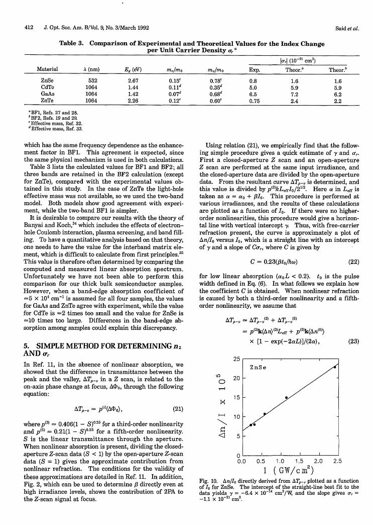
wherep(3) - 0.406(1 - S)025 for a third-order nonlinearityand p(r) 0.21(1 - S)02 5 for a fifth-order nonlinearity.S is the linear transmittance through the aperture.When nonlinear absorption is present, dividing the closed-aperture Z-scan data (S < 1) by the open-aperture Z-scandata (S = 1) gives the approximate contribution fromnonlinear refraction. The conditions for the validity ofthese approximations are detailed in Ref. 11. In addition,Fig. 2, which can be used to determine p directly even athigh irradiance levels, shows the contribution of 2PA tothe Z-scan signal at focus.
Using relation (21), we empirically find that the follow-ing simple procedure gives a quick estimate of y and ,.First a closed-aperture Z scan and an open-apertureZ scan are performed at the same input irradiance, andthe closed-aperture data are divided by the open-aperturedata. From the resultant curve AT,-, is determined, andthis value is divided by p(3)kLeffIO/212 . Here a in Leff istaken as a = a0 + 1Io. This procedure is performed atvarious irradiances, and the results of these calculationsare plotted as a function of Io. If there were no higher-order nonlinearities, this procedure would give a horizon-tal line with vertical intercept . Thus, with free-carrierrefraction present, the curve is approximately a plot ofAn/IO versus Io, which is a straight line with an interceptof y and a slope of Co-r, where C is given by
C 0.23(,to/hw) (22)
for low linear absorption (aoL < 0.2). to is the pulsewidth defined in Eq. (6). In what follows we explain howthe coefficient C is obtained. When nonlinear refractionis caused by both a third-order nonlinearity and a fifth-order nonlinearity, we assume that
ATp-v ATp( 3) + AT (5)
P(3)k(Afn)(3)Leff + p(5)k(An(5 )
)
x [1 - exp(-2aL)]/(2a), (23)
25
tO
CDV.1
20
5
10
< 5
0 0.0 0.5 1.0 1.5 2.0 2.5
I (GW/c m2 )Fig. 10. An/Io directly derived from ATp- plotted as a functionof Io for ZnSe. The intercet of the straight-line best fit to thedata yields y = -6.4 x 10 4 cm2/W, and the slope gives ar =-1.1 x 1-21 cm3.
Said et al.
ATp-,, = p(')(A(Do),
Vol. 9, No. 3/March 1992/J. Opt. Soc. Am. B 413
20
0 15
10I:
\,5
0 L0.0 0.1 0.2 0.3 0.4
I (GW/cm')
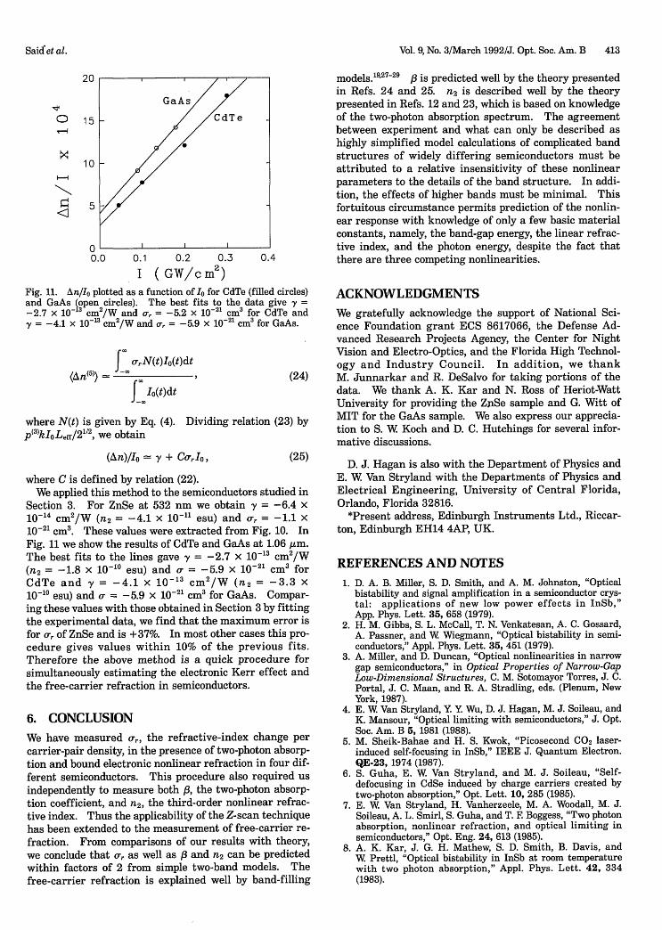
Fig. 11. An/Io plotted as a function of Io for CdTe (filled circles)and GaAs open circles). The best fits to the data give }y =-2.7 x 10 I cm2 /W and err = -5.2 x 10⁻² ' cm3 for CdTe andy = -4.1 X 101-3 cm2 /W and or = -5.9 x 10⁻²¹ cm
3 for GaAs.
( | , rN(t)Io(t)dt(Avn(5) ) , . (24)
| Io(t)dt
where N(t) is given by Eq. (4). Dividing relation (23) byp 3)kIoLeff/2 2, we obtain
(An)/Io + CIo, (25)
where C is defined by relation (22).We applied this method to the semiconductors studied in
Section 3. For ZnSe at 532 nm we obtain y = -6.4 x10⁻¹⁴ cm 2 /W (n2 = -4.1 x 10⁻¹¹ esu) and ar = -1.1 X10⁻²¹ cm3. These values were extracted from Fig. 10. InFig. 11 we show the results of CdTe and GaAs at 1.06 ,um.The best fits to the lines gave y = -2.7 x 10-'3 cm2 /W(n2 = -1.8 x 10`0 esu) and ar = -5.9 x 10⁻²¹ cm3 forCdTe and y = -4.1 x 10⁻¹³ cm 2 /W (n 2 = -3.3 x10⁻¹⁰ esu) and a = -5.9 x 10⁻²¹ cm 3 for GaAs. Compar-ing these values with those obtained in Section 3 by fittingthe experimental data, we find that the maximum error isfor Ar of ZnSe and is +37%. In most other cases this pro-cedure gives values within 10% of the previous fits.Therefore the above method is a quick procedure forsimultaneously estimating the electronic Kerr effect andthe free-carrier refraction in semiconductors.
6. CONCLUSION
We have measured a,, the refractive-index change percarrier-pair density, in the presence of two-photon absorp-tion and bound electronic nonlinear refraction in four dif-ferent semiconductors. This procedure also required usindependently to measure both 63, the two-photon absorp-tion coefficient, and n2 , the third-order nonlinear refrac-tive index. Thus the applicability of the Z-scan techniquehas been extended to the measurement of free-carrier re-fraction. From comparisons of our results with theory,we conclude that , as well as /3 and n2 can be predictedwithin factors of 2 from simple two-band models. Thefree-carrier refraction is explained well by band-filling
models.'9 27-29 6 is predicted well by the theory presented
in Refs. 24 and 25. n 2 is described well by the theorypresented in Refs. 12 and 23, which is based on knowledgeof the two-photon absorption spectrum. The agreementbetween experiment and what can only be described ashighly simplified model calculations of complicated bandstructures of widely differing semiconductors must beattributed to a relative insensitivity of these nonlinearparameters to the details of the band structure. In addi-tion, the effects of higher bands must be minimal. Thisfortuitous circumstance permits prediction of the nonlin-ear response with knowledge of only a few basic materialconstants, namely, the band-gap energy, the linear refrac-tive index, and the photon energy, despite the fact thatthere are three competing nonlinearities.
ACKNOWLEDGMENTSWe gratefully acknowledge the support of National Sci-ence Foundation grant ECS 8617066, the Defense Ad-vanced Research Projects Agency, the Center for NightVision and Electro-Optics, and the Florida High Technol-ogy and Industry Council. In addition, we thankM. Junnarkar and R. DeSalvo for taking portions of thedata. We thank A. K. Kar and N. Ross of Heriot-WattUniversity for providing the ZnSe sample and G. Witt ofMIT for the GaAs sample. We also express our apprecia-tion to S. W Koch and D. C. Hutchings for several infor-mative discussions.
D. J. Hagan is also with the Department of Physics andE. W Van Stryland with the Departments of Physics andElectrical Engineering, University of Central Florida,Orlando, Florida 32816.
*Present address, Edinburgh Instruments Ltd., Riccar-ton, Edinburgh EH14 4AP, UK.
REFERENCES AND NOTES
1. D. A. B. Miller, S. D. Smith, and A. M. Johnston, "Opticalbistability and signal amplification in a semiconductor crys-tal: applications of new low power effects in InSb,"App. Phys. Lett. 35, 658 (1979).
2. H. M. Gibbs, S. L. McCall, T. N. Venkatesan, A. C. Gossard,A. Passner, and W Wiegmann, "Optical bistability in semi-conductors," Appl. Phys. Lett. 35, 451 (1979).
3. A. Miller, and D. Duncan, "Optical nonlinearities in narrowgap semiconductors," in Optical Properties of Narrow-GapLow-Dimensional Structures, C. M. Sotomayor Torres, J. C.Portal, J. C. Maan, and R. A. Stradling, eds. (Plenum, NewYork, 1987).
4. E. W Van Stryland, Y Y. Wu, D. J. Hagan, M. J. Soileau, andK. Mansour, "Optical limiting with semiconductors," J. Opt.Soc. Am. B 5, 1981 (1988).
5. M. Sheik-Bahae and H. S. Kwok, "Picosecond CO2 laser-induced self-focusing in InSb," IEEE J. Quantum Electron.Q-23, 1974 (1987).
6. S. Guha, E. W Van Stryland, and M. J. Soileau, "Self-defocusing in CdSe induced by charge carriers created bytwo-photon absorption," Opt. Lett. 10, 285 (1985).
7. E. W Van Stryland, H. Vanherzeele, M. A. Woodall, M. J.Soileau, A. L. Smirl, S. Guha, and T. F. Boggess, "Two photonabsorption, nonlinear refraction, and optical limiting insemiconductors," Opt. Eng. 24, 613 (1985).
8. A. K. Kar, J. G. H. Mathew, S. D. Smith, B. Davis, andW Prettl, "Optical bistability in InSb at room temperaturewith two photon absorption," Appl. Phys. Lett. 42, 334(1983).
Said et al.

414 J. Opt. Soc. Am. B/Vol. 9, No. 3/March 1992
9. E. Canto-Said, D. J. Hagan, J. Young, and E. W Van Stryland,"Degenerate four-wave mixing measurements of high ordernonlinearities in semiconductors," IEEE J. QuantumElectron. 27, 2274 (1991); D. J. Hagan, E. Canto, E. Meisak,M. J. Soileau, and E. W Van Stryland, "Picosecond degener-ate four-wave mixing studies in ZnSe," in Conference onLasers and Electro-Optics, Vol. 7 of 1988 OSA TechnicalDigest Series (Optical Society of America, Washington, D.C.,1988), p. 160.
10. A. A. Said, M. Sheik-Bahae, D. J. Hagan, E. J. Canto-Said,Y Y Wu, J. Young, T. H. Wei, and E. W Van Stryland, "Non-linearities in semiconductors for optical limiting," in Electro-Optical Materials for Switches, Coatings, Sensor Optics,and Detectors, R. Hartmann and M. J. Soleau, eds., Proc.Soc. Photo-Opt. Instrum. Eng. 1307, 294 (1990).
11. M. Sheik-Bahae, A. A. Said, T. H. Wei, D. J. Hagan, and E. WVan Stryland, "Sensitive measurement of optical nonlineari-ties using a single beam," IEEE J. Quantum Electron. 26,760 (1990).
12. M. Sheik-Bahae, D. J. Hagan, and E. W. Van Stryland,"Dispersion and band-gap scaling of the electronic Kerr ef-fect in solids associated with two-photon absorption,"Phys. Rev. Lett. 65, 96 (1990).
13. M. Sheik-Bahae, A. A. Said, and E. W Van Stryland, "High-sensitivity, single-beam n2 measurement," Opt. Lett. 14, 955(1989).
14. A. E. Kaplan, "External self-focusing of light by a nonlinearlens," Radiophys. Quantum Electron. 12, 692 (1969).
15. S. A. Akhmanov, R. V Khokhlov, and A. P. Sukhorukov, "Self-focusing, self-defocusing, and self-modulation of laserbeams," in Laser Handbook, F. T. Arecchi and E. 0. Shultz-Dubois, eds. (North-Holland, Amsterdam, 1972), Vol. 2,p. 1151.
16. J. H. Bechtel and W L. Smith, "Two-photon absorption insemiconductors with picosecond pulses," Phys. Rev. B 13,3515 (1976).
17. E. W Van Stryland, M. A. Woodall, H. Vanherzeele, and M. J.Soileau, "Energy band-gap dependence of two-photon absorp-tion," Opt. Lett. 10, 490 (1985).
18. T. F. Boggess, A. L. Smirl, S. C. Moss, I. W Boyd, and E. WVan Stryland, "Optical limiting in GaAs," IEEE J. QuantumElectron. QE-21, 488 (1985).
19. D. A. B. Miller, C. T. Seaton, M. E. Prise, and S. D. Smith,"Band-gap-resonant nonlinear refraction in III-V semicon-ductors," Phys. Rev. Lett. 47, 197 (1981).
20. J. D. Gaskill, Linear Systems, Fourier Transforms, andOptics (Wiley, New York, 1978).
21. The ZnSe sample was obtained from Heriot-Watt University,
Edinburgh, UK; CdTe II-VI, from Saxonburgh, Pa.; GaAsfrom the Massachusetts Institute of Technology, Boston,Mass.; and ZnTe from Cleveland Crystals, Cleveland, Ohio.
22. A. L. Smirl, T. F. Boggess, J. Dubard, and A. G. Cui, "Singleand multiple beam nonlinear absorption and refraction mea-surements in semiconductors," in Electro-Optical Materialsfor Switches, Coatings, Sensor Optics, and Detectors,R. Hartmann and M. J. Soileau, eds., Proc. Soc. Photo-Opt.Instrum. Eng. 1307, 251 (1990).
23. M. Sheik-Bahae, D. Hutchings, D. J. Hagan, and E. WVan Stryland, "Dispersion of bound electronic nonlinearrefraction in solids," IEEE J. Quantum Electron. 27, 1296(1991).
24. M. Weiler, "Nonparabolicity and exciton effects in two photonabsorption in zinc-blende semiconductors," Solid State Com-mun. 39, 937 (1981).
25. B. S. Wherrett, "Scaling rules for multiphoton interband ab-sorption in semiconductors," J. Opt. Soc. Am. B 1, 67 (1984).
26. C. C. Lee and H. Y Fan, "Two photon absorption with exci-ton effects for degenerate valence bands," Phys. Rev. B 9,3502 (1974).
27. A. G. Aronov, D. E. Pikus, and D. Sh. Shekhter, "Quantumtheory of free-electron dielectric constant in semiconduc-tors," So. Phys. Solid State 10, 645 (1968).
28. D. H. Auston, S. McAffee, C. V Shank, E. P. Ippen, and0. Teschke, "Picosecond spectroscopy of semiconductors,"Solid State Electron. 21, 147 (1978).
29. B. S. Wherrett, A. C. Walker, and F. A. P. Tooley, "Nonlinearrefraction for cw optical bistability," in Optical Nonlineari-ties and Instabilities in Semiconductors, H. Haug, ed. (Aca-demic, New York, 1988), p. 239.
30. T. S. Moss, "Theory of intensity dependence of refractiveindex," Phys. Status Solidi B 101, 555 (1980).
31. E. 0. Kane, "Band structure of InSb," J. Chem. Phys. Solids1, 249 (1957).
32. K.-H. Hellwege, editor, Landolt-Bdrnstein Numerical Dataand Functional Relationships in Science and Technology,Vol. 17, Semiconductors (Springer-Verlag, New York, 1982),Subvol. (b).
33. R. K. Jain and M. B. Klein, "Degenerate four-wave mixing insemiconductors," in Optical Phase Conjugation, R. A.Fisher, ed. (Academic, New York, 1983), p. 335.
34. L. Banyai and S. W Koch, 'A simple theory for the effects ofplasma screening on the optical spectra of highly excitedsemiconductors," Z. Phys. B 63, (1986).
35. S. W Koch, Optical Sciences Center, University of Arizona,Tucson, Ariz. 85721 (personal communication).
Said. et al.