
Dependence of dark current on zinc concentration in Zn x Cd 1− x S/ZnTe heterojunctions
12
Solar Energy Materials and Solar Cells 29 (1993) 97-108 North-Holland Solar Energy Materials and Solar Cells Dependence of dark current on zinc concentration in ZnxCdl_xS/ZnTe heterojunctions M. Abdel Naby, A. Zekry, F. E1 Akkad and H.F. Ragaie Electrical Engineering Department, College of Engineering, King Saud University, P.O. Box 800, Riyadh 11421, Saudi Arabia Received 12 December 1989; in revised form 19 August 1991 ZnxCdl_/S/ZnTe heterojunctions were fabricated by radio frequency (RF) sputtering of n-type ZnxCd l_xS thin films on phosphorus doped p-type ZnTe single crystals. Current-voltage and capacitance-voltage characteristics of these heterojunctions were studied. Especially, the influence of Zn concentration x in the ZnxCdl_~S layer on the characteristics of the hetero- junction was investigated. The complicated dependence of the reverse saturation current J0 on the Zn concentration in the film material was explained. I. Introduction Aiming to develop a p-n heterojunction from wide band gap semiconductors, Aven et al. [1] prepared and investigated a heterojunction consisting of CdS over ZnTe. Further studies were carried out by a number of research groups [2-5] to determine the conduction mechanisms in this structure and its solar cell parame- ters. However, the majority of the work already conducted was devoted to the electrical properties of the junction with emphasis on the minority carrier injection mechanism because of its importance for electroluminescense applications. Dark I-V characteristics were studied for junctions prepared by evaporation techniques [1,2], vapour deposition of CdS on ZnTe single crystal [3] and chemical transport reactions [5]. In order to explain the dark current conduction mechanism in CdS/ZnTe heterojunctions, it was assumed that the junctions have a psn structure, where s stands for "semi-insulating" layer. The s-layer in the junctions prepared by Pfisterer and Schock [2] is likely due to a heavily compensated region as a result of copper diffusion into the CdS. Ota et al. [4] suggested that the s-layer is due to ZnxCdl_xTe alloy formed as a result of inter-diffusion at the interface. In order to improve the electron affinity mismatch, Kimmerle et al. [6] and Arndt et al. [7] replaced CdS with a mixed sulphide layer ZnxCd 1 xS using the evaporation technique. Since a high preparation temperature is known to enhance inter-diffusion leading to the formation of an interface s-layer, the properties of a structure free Correspondence to." A. Zekry, Electrical Engineering Department, College of Engineering, King Saud University, P.O. Box 800, Riyadh 11421, Saudi Arabia. 0927-0248/93/$06.00 © 1993 - Elsevier Science Publishers B.V. All rights reserved
Transcript of Dependence of dark current on zinc concentration in Zn x Cd 1− x S/ZnTe heterojunctions

Solar Energy Materials and Solar Cells 29 (1993) 97-108 North-Holland
Solar Energy Materials and Solar Cells
Dependence of dark current on zinc concentration in ZnxCdl_xS/ZnTe heterojunctions
M. Abde l Naby, A. Zekry , F. E1 Akk ad and H.F. Raga ie
Electrical Engineering Department, College of Engineering, King Saud University, P.O. Box 800, Riyadh 11421, Saudi Arabia
Received 12 December 1989; in revised form 19 August 1991
ZnxCdl_/S/ZnTe heterojunctions were fabricated by radio frequency (RF) sputtering of n-type ZnxCd l_xS thin films on phosphorus doped p-type ZnTe single crystals. Current-voltage and capacitance-voltage characteristics of these heterojunctions were studied. Especially, the influence of Zn concentration x in the ZnxCdl_~S layer on the characteristics of the hetero- junction was investigated. The complicated dependence of the reverse saturation current J0 on the Zn concentration in the film material was explained.
I. Introduction
Aiming to develop a p - n heterojunction from wide band gap semiconductors, Aven et al. [1] prepared and investigated a heterojunction consisting of CdS over ZnTe. Further studies were carried out by a number of research groups [2-5] to determine the conduction mechanisms in this structure and its solar cell parame- ters. However, the majority of the work already conducted was devoted to the electrical properties of the junction with emphasis on the minority carrier injection mechanism because of its importance for electroluminescense applications.
Dark I - V characteristics were studied for junctions prepared by evaporation techniques [1,2], vapour deposition of CdS on ZnTe single crystal [3] and chemical transport reactions [5].
In order to explain the dark current conduction mechanism in C d S / Z n T e heterojunctions, it was assumed that the junctions have a psn structure, where s stands for "semi-insulating" layer. The s-layer in the junctions prepared by Pfisterer and Schock [2] is likely due to a heavily compensated region as a result of copper diffusion into the CdS. Ota et al. [4] suggested that the s-layer is due to ZnxCdl_xTe alloy formed as a result of inter-diffusion at the interface.
In order to improve the electron affinity mismatch, Kimmerle et al. [6] and Arndt et al. [7] replaced CdS with a mixed sulphide layer ZnxCd 1 xS using the evaporation technique.
Since a high preparation temperature is known to enhance inter-diffusion leading to the formation of an interface s-layer, the properties of a structure free
Correspondence to." A. Zekry, Electrical Engineering Department, College of Engineering, King Saud University, P.O. Box 800, Riyadh 11421, Saudi Arabia.
0927-0248/93/$06.00 © 1993 - Elsevier Science Publishers B.V. All rights reserved
98 M. Abdel Naby et al. / ZnxCd l _ xS / ZnTe heterojunctions
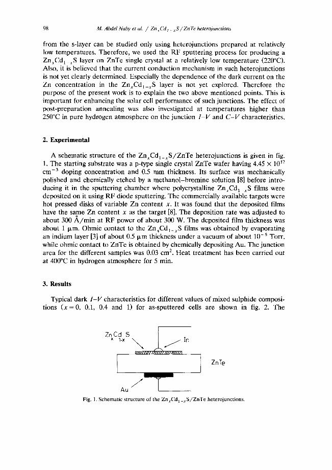
from the s-layer can be studied only using heterojunctions prepared at relatively low temperatures. Therefore, we used the RF sputtering process for producing a ZnxCdl_~S layer on ZnTe single crystal at a relatively low temperature (220°C). Also, it is believed that the current conduction mechanism in such heterojunctions is not yet clearly determined. Especially the dependence of the dark current on the Zn concentration in the Zn~Cdl_xS layer is not yet explored. Therefore the purpose of the present work is to explain the two above mentioned points. This is important for enhancing the solar cell performance of such junctions. The effect of post-preparation annealing was also investigated at temperatures higher than 250°C in pure hydrogen atmosphere on the junction I - V and C - V characteristics.
2. Experimental
A schematic structure of the Z n x C d l _ x S / Z n T e heterojunctions is given in fig. 1. The starting substrate was a p-type single crystal ZnTe wafer having 4.45 × 1017 cm -3 doping concentration and 0.5 mm thickness. Its surface was mechanically polished and chemically etched by a methanol-bromine solution [8] before intro- ducing it in the sputtering chamber where polycrystalline ZnxCdt_xS films were deposited on it using RF diode sputtering. The commercially available targets were hot pressed disks of variable Zn content x. It was found that the deposited films have the same Zn content x as the target [8]. The deposition rate was adjusted to
o
about 300 A / m i n at RF power of about 300 W. The deposited film thickness was about 1 ~m. Ohmic contact to the ZnxCd t_x S films was obtained by evaporating an indium layer [3] of about 0.5 ~m thickness under a vacuum of about 10 -5 Torr, while ohmic contact to ZnTe is obtained by chemically depositing Au. The junction area for the different samples was 0.03 cm 2. Heat treatment has been carried out at 400°C in hydrogen atmosphere for 5 min.
3. Results
Typical dark I - V characteristics for different values of mixed sulphide composi- tions (x = 0, 0.1, 0.4 and 1) for as-sputtered cells are shown in fig. 2. The
ZnCd S x 1-x
Au
I I I I t ' l l l l l l l l I
/ T
ZnTe
Fig. 1. Schematic structure of the ZnxCd I xS/ZnTe heterojunctions.

M. Abdel Naby et al. / ZnxCd I xS / Zn Te heterojunctions 99
E o 2 <
I ~)4
~5 6
X=O.1
1
oo o5
v(v)
Fig. 2. Dark I -V characteristics of ZnxCd I xS/ZnTe heterojunctions with various zinc concentration x (x = 0, 0.1, 0.4 and 1).
corresponding computed values of the ideality factor n and reverse saturation current density J0 are given in table 1.
The values of n observed from the table ranges from 1.5 to 2.6. The values of the reverse saturation current density given in table 1 fall in the range 10-6-10 -7 A / c m 2 as reported by other authors [1,2]. Fig. 3 shows the variation of the measured reverse saturation current density J0 as a function of composition x. It can be seen that J0 increases with Zn concentration reaching a maximum at x = 0.1, then decreases again.
In order to explain the variation of J0 with Zn concentration we have to measure the junction capacitance as a function of Zn concentration. Therefore, the measured capacitance as a function of Zn concentration is shown in fig. 4. It can be seen from it that the capacitance decreases with Zn concentration x. Consequently, the width of the space charge region, W, increases with the composition x. Furthermore, typical C - 2 - V characteristics for representative samples are shown in fig. 5. It is clear from it that C -2 increases almost linearly with the reverse voltage. Consequently the carrier concentration is homogeneous in the film region adjacent to the equilibrium space charge region. If there is any semi-insulating layer at the interface it will be within the space charge region at thermal equilibrium. Since the sputtering temperature is low for an effective mixing to occur at the interface, it is reasonable to assume an abrupt heterojunc- tion for as sputtered specimens.
The effect of annealing the samples in H 2 at 400°C for 5 min on the I - V characteristics is given in fig. 6. A change in the value of n from 2.6 before

100 M. Abdel Naby et al. / ZnxCd ~ _ ~S / Zn Te heterojunctions
i ° °
o ~
~.~ ~ - ~
~ 2 ~ 4
~ ~
N
s ~ r
= N S . = _ ~ N 's
] 1 1 1
X X X X
X X X X

M. Abdel Naby et al. / ZnxCd I _ xS / ZnTe heterojunctions I01
105 f % u
T o
L
O0 ' ' ' ' ' . '8 0.2 0.4 0.6 0
x Fig. 3. Reverse saturation current J0 as a function of composition x of ZnxCd l_xS/ZnTe heterojunc-
tions.
annea l ing to 1.5 after annea l ing was found. Also Jo increased from 2 X 10 -7 before annea l ing to 8 X 10 -6 A / c m 2 after anneal ing . Fig. 7 shows typical be-
haviour of the junc t ion capaci tance upon annea l ing the samples. In addi t ion to the
0 . .
~ J
1400
1000
600
200
i
QO
V=.QO
i i i i
0.2 04 0.6 0.8 X
Fig. 4. Junction capacitance C as a function of composition x of ZnxCd 1 xS/ZnTe samples.

102 M. Abdel Naby et al. / Zn~Cd I _ ~S / ZnTe heterojunctions
i 13. O.
r t-~/x
C)
8O
70
60
50
40
30
20 X --0,1
lO
I t
-2 -1 0
v ( v )
Fig. 5. Typical C -2 versus V of ZnxCd I _ x S / Z n T e samples with different values of x.
1 (32
16 4
-6 10
t I
0.0 0.5
V ( V )
Fig. 6. Annealing effect on dark I - V characteristics for Zno.4Cdo.6S/ZnTe heterojunction.

M. Abdel Naby et al. / Zn xCd ~ xS / Zn Te heterojunctions 103
600
'7, k l -
O _ v
~ o z, O0
6.0
5.0
\
I I
-15 - i 0 -0.5 oo
v ( v )
Fig. 7. Annealing effect on C - 2 - V characteristics of the CdS/ZnTe heterojunction. (A) Before annealing, (B) after annealing.
reduction of the junction capacitance, a deviation of C-2-V from linearity was noted after annealing, presumably due to the effect of chemical mixing at the interface as proposed by Ota et al. [4]. Values of about 3.5 x 10¹⁵ and 4.7 x 10 a2 cm -3 were obtained for the electron concentration before and after heat treat- ment, at low reverse bias, respectively.
4. Discussion
The observed behaviour of J0 with the Zn concentration x (fig. 3) and with annealing can be interpreted by considering the various parameters limiting the value of J0.
According to the C - V curves one can differentiate between two structures: an abrupt heterojunction for as-sputtered devices and a pin structure after annealing. In the next sections we shall treat each one separately.
4.1. The abrupt heterojunction model f o r as-sputtered devices
The dark current components are (i) the recombination current in the neutral regions, (ii) the recombination current in the space charge region and (iii) the recombination current at the interface states between the two materials of the

104 M. Abdel Naby et aL / Zn xCd I _ xS / ZnTe heterojunctions
heterojunction. The current components (i) and (ii) are negligible in comparison to measured currents because of the wide bandgaps of the substrate and film materials and hence the very low intrinsic carrier concentrations. Consequently, component (iii) is dominant over the others. The first indication of the dominance of this component is its characteristic variation of the ideality factor. The ideality factor n of this component can vary from unity to large values depending on the doping levels in both sides of the junction and on the interface charges.
The interface recombination current J can be expressed by
J = e C n C _ [ N s s (__Pslns2 - n z ) d E ) , (1 )
where C n (Cp) is the capure coefficients of electrons (holes), n s (P~) is the electron (hole) concentration at the surface, n i is the intrinsic concentration of the base material, n 1 (P1) is the electron concentration in the conduction band if Ef ~ E t the trap level within the energy gap and Nss is the surface state density.
For all recombination centers lying deep enough in the band gap such that n 1 and P1 are much smaller than the sum of the majority carrier concentration on both sides (Psi + ns2) and assuming that C. = Co, the above expression reduces to
J = e g n N s t , (2) (Ps, +ns2)
where Nst = fNss dE- the deep lying surface trap density~era 2. According to Boltzmann statistics Psl and ns2 are given by
Ps, =P0~ e x p [ - ( 6 , - V1)/ /VT] (3)
and
ns2 = no2 exp[ - (4)2 - V 2 ) / V r ] , (4)
where P01 is the hole concentration in ZnTe, ~b~ is the equilibrium potential barrier height in ZnTe, V~ is the junction voltage drop in ZnTe, no2 is the electron concentration in ZnCdS films, 02 is the equilibrium potential barrier height in ZnCdS, V 2 is the junction voltage drop in ZnCdS, V T is the thermal voltage ( k T / e ) , 1/1 + V 2 = V is the applied junction voltage, and ~D 1 ~- (~2 = (b is the contact difference of potential between the two materials.
For our heterojunctions the electron concentration in the film n0z is much smaller than the hole concentration P0a in the substrate material and ¢k~ - V, --- ~2
- V 2 since the ideality factor is nearly 2. It follows from (2) and (3) that P~, is much larger than ns2. With this inequality, eq. (2) reduces to
J = eCnNstno2 e x p ( - - ( ~ 2 / V T ) e x p ( V 2 / V T ) . (5)
By definition the ideality factor n is related to V 2 by
n = V / V 2. (6)
Inserting (6) in (5) one gets finally
J = eC, Nstnoz exp(--ck2/VT) e x p ( V / n V T ) =-Jo e x p ( V / n V T ) , (7)

M. Abdel Naby et al. / ZnxCd ! _ xS / Zn Te heterojunctions 105
.° I
, N ( x )
.Ni$
NA
m it
Fig. 8. Space charge distribution in an abrupt heterojunction with positive interface charge Nis.
where J0 is the reverse saturation current. From (7) it has the form
Jo = e f n g s t n 0 2 e x p ( - - ¢ 2 / V T ) . (8)
It is clear from (8) that the reverse saturation current of our junctions is propor- tional to the electron concentration in the ZnCdS film. On the other hand, it decreaes exponentially with the built-in voltage 4)2-
The built-in potential ~b 2 is related to the doping concentrations N D and N A on both sides of the junction and to the interface charge density Nis. The interface charge must be positive because the measured potential barrier t~m is smaller than the theoretical o n e ~bth [15]. Based on simple electrostatics one can prove for the abrupt junction with the one-dimensional charge distribution shown in fig. 8 that:
~b 1 = ~bs [(/p0///s) 2 - 1],
~b2 = ~bm - (~1
t~m = ~th -- ~s ,
l s = N i s / N A ,
Nis = ( 2eNAqbs/e ) °'5,
lP° NA + ND NA + ND
(9)
(10)
(11)
(12a)
(12b)
2e ND~m ]0.5
+ e ~ NA +ND ] - - - - ' (13)
where ths is the reduction in the theoretical contact difference of potential due to the positive interface charges, l s is the width of the space charge in the substrate due to the positive interface charges, lp0 is the width of the depletion region in the substrate at thermal equilibrium and • is the dielectric constant of the substrate.
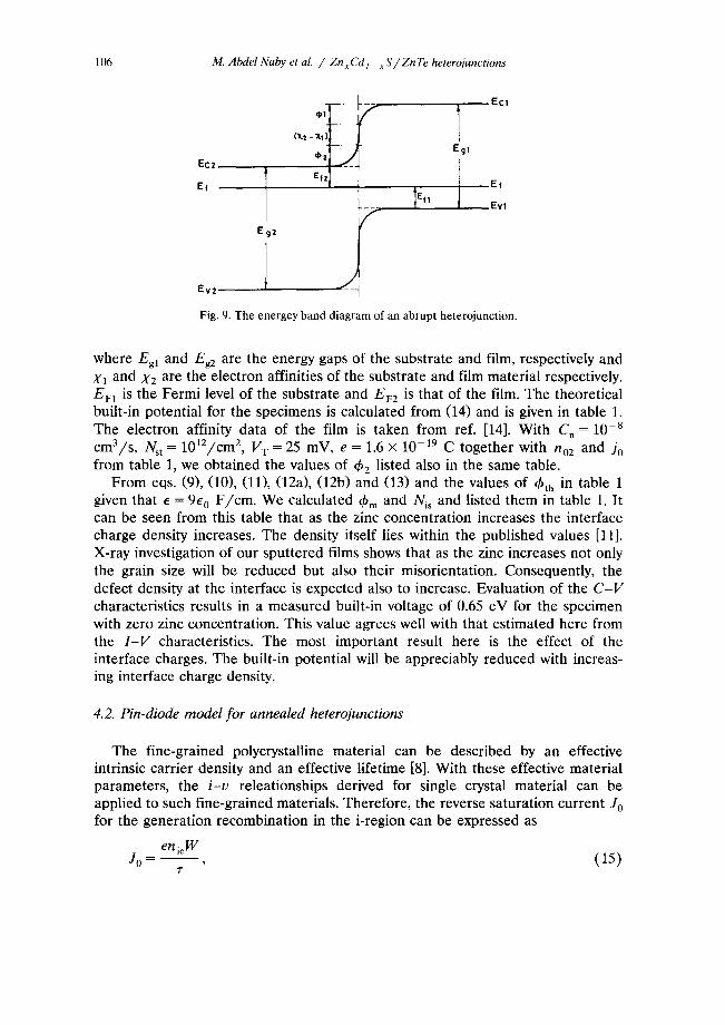
From the energy level diagram in fig. 9 the theoretical built-in voltage ~bth can be expressed by
~bth = Ega --' EF2 - Eva - (X2 - X , ) , (14)
106 M. Abdel Naby et al. / ZnxCd I xS / ZnTe heterojunctions
Ec2
Ef
Ev2
°,F/ Efz I
,y Eg2
J Ell
ECl
1 Egl
El
Evl
Fig. 9. The energey band diagram of an abrupt heterojunction.
where Eg 1 and Eg 2 are the energy gaps of the substrate and film, respectively and Xl and Xz are the electron affinities of the substrate and film material respectively. Evl is the Fermi level of the substrate and EF2 is that of the film. The theoretical built-in potential for the specimens is calculated from (14) and is given in table 1. The electron affinity data of the film is taken from ref. [14]. With C n = 10 -8 cm3/s, Nst = 1012/cm 2, V T = 25 mV, e = 1.6 × 10 -19 C together with n02 and J0 from table 1, we obtained the values of ~)2 listed also in the same table.
From eqs. (9), (10), (11), (12a), (12b) and (13) and the values of ~bth in table 1 given that e = 9e 0 F /cm. We calculated &m and Nis and listed them in table 1. It can be seen from this table that as the zinc concentration increases the interface charge density increases. The density itself lies within the published values [11]. X-ray investigation of our sputtered films shows that as the zinc increases not only the grain size will be reduced but also their misorientation. Consequently, the defect density at the interface is expected also to increase. Evaluation of the C - V characteristics results in a measured built-in voltage of 0.65 eV for the specimen with zero zinc concentration. This value agrees well with that estimated here from the I - V characteristics. The most important result here is the effect of the interface charges. The built-in potential will be appreciably reduced with increas- ing interface charge density.
4.2. Pin-diode model for annealed heterojunctions
The fine-grained polycrystalline material can be described by an effective intrinsic carrier density and an effective lifetime [8]. With these effective material parameters, the i -v releationships derived for single crystal material can be applied to such fine-grained materials. Therefore, the reverse saturation current J0 for the generation recombination in the i-region can be expressed as
e n ie W Jo = - - , (15)
1"

M. Abdel Naby et al. / ZnxCd I _ xS / Zn Te heterojunctions 107
where W is the i-layer width, nie is the effective intrinsic carrier density, e is the electron charge and ~- is the effective lifetime in the space charge region due to recombination via deep-lying electronic states in the energy gap.
Due to chemical mixing of the substrate material (ZnTe) and the film material (ZnCdS) a ternary compound results which has lower energy gap. The energy gap is an average value for the energy gap of the compounds CdTe and ZnS; since these two compounds may constitute the complex compound of the interface layer. Therefore, the energy gap Eg i of the i-layer is estimated to be 1.86 eV.
In highly disordered material band tails will be formed [10]. Deviations from stoichiometry may also cause band tails. The electronic states in the band tails near the band edges are not localized. The higher the atomic disorder in the material is, the larger are the band tails. Consequently, the effective electrical gap is smaller than the optical energy gap. In addition, field assisted generation of e lectron-hole pairs occurs in fine-grained polycrystalline material due to band bending [11]. The measured activation energy of the conductivity amounts to 0.27 eV [8]. This activation energy is equal to the barrier height between two adjacent grains [12].
All these effects can be formally modeled by energy gap narrowing A Eg while keeping the effective density of states unchanged [13]. Without bandgap narrowing the intrinsic carrier concentration is expressed by
n~ = NoN v e x p ( - E g / K T ) , (16)
where N c and N v are the effective density of states in the conduction and valence bands respectively. With an effective bandgap narrowing A E g , w e can write
n2e = N c N v e x p ( - E g / K T ) exp( A E g / K T ) , (16a)
where nie is the effective intrinsic concentration. Combining (16) and (16a) we get
n2¢ = n 2 exp( A E g / K T ) . (17)
From this discussion it is clear that for fine-grained polycrystalline material with high volume defects, which is the case in our sputtered films, the effective electrical energy gap may be appreciably smaller than the optical bandgap. Consequently, the effective intrinsic carrier concentration will be much higher than its value in monocrystalline material.
The lifetime in the i-region depends on the density of the localized electronic states inside the crystallites and at their grain boundaries. Assuming spherical grains with diameter dg an average volume trap density Ntv = 6Nst/dg can be calculated. The lifetime ~- can then be expressed by [8]
1 dg
~" ~VthNt ~ 6¢rVthNs ' , (18)
where o- is the capture cross-section for electrons and holes and Vtn is the thermal velocity of mobile carriers.
Combining eqs. (15), (16) and (18) and substituting dg= 400 ,~ (as measured by 13 2 7 19 3 X-rays), W = 10 - 4 cm, or= 10- c m , Vth = 10 cm/s , N c ~ v = 10 cm- , and

108 M. Abdel Naby et al. / Znx Cd l - x S / Zn Te heterojunctions
the measured value of the reverse sa turat ion cur ren t density of 8 × 10 -6 A / c m 2, the effective thermal energy gap Eg t is es t imated to be 1.6 eV. This value is slightly smaller than the es t imated real value for the i-layer because of the effective band gap norrowing explained previosly. The difference amount s to the barr ier height be tween two adjacent grains.
In order to confirm the validity of the model , one has to measure the tempera- ture dependence of the I - V characteristics to de te rmine the activation energy.
5. Conclusion
The R F sput ter ing technique is used to prepare Z n x C d l _ x S / Z n T e heterojunc- t ions at ralatively low tempera ture . It was found that the cur ren t is dominant ly a genera t ion recombina t ion at the interface of as-sput tered heterojunct ions . The interface charge density increases with increased zinc concen t ra t ion in the film. It amoun t s to ( 1 - 2 ) × 1012/cm 2. After anneal l ing, the cur ren t is domina ted by
recombina t ion in an interface region. This interface region is buil t by mixing the film and substrate material . It has a lower band gap than that of the substrate and
film materials.
References
[1] M. Aven and D.M. Cook, J. Appl. Phys. 32 (1961) 960. [2] F. Pfisterer and H.W. Schock, J. Cryst. Growth 59 (1982) 432. [3] M. Aven and W.M. Garwaki, J. Electrochem. Soc. 110 (1963) 403. [4] T. Ota, K. Kobayashi and K. Takahashi, J. Appl. Phys. 45 (1974) 1750. [5] Y.A. Fedotov, V.K. Supalov, T.P. Manuilova, A.V. Vankukov and N.M. Kondourav, Sov. Phys.
Semiconductor 5 (1972) 1530. [6] J, Kimmerle, R. Menner, F. Pfisterer and H.W. Schock, J. Cryst. Growth 72 (1985) 525. [7] W. Arndt, B. Dimmler, H. Dittrich, J. Kimmerle, R. Menner, F. Pfisterer and H.W. Schock, 18th
IEEE PVSC, Las Vegas (1985) p. 1671. [8] M. Abd Elnaby, Ph.D. Thesis, Ain Shams University, Cairo, Egypt (1988). [9] B.L. Sharma and R.K. Purohit, Semiconductor Heterojunctions (Pergamon Press, New York,
1974). [10] F.A. Lindholm and Ching Sah, IEEE Trans. Electron Dev. ED-24 (1977) 299. [11] M. Bujatti and F. Marcelja, Thin Solid Films 11 (1972) 249. [12] T. Kamins, Polycrystalline Silicon for Integrated Circuit Applications (Kluwer, Dordrecht, 1988)
pp. 197-202. [13] R.P. Mertens, R.J. Van Overstraeten and H.J. De Man, Adv. Electron. Electron Phys. 55 (1988)
77. [14] T.M. Razykov and B.Kh. Kadirov, Phys. Stat. Sol. (a) 84 (1984) K71. [15] A. Zekry, M. Abd EI-Naby, H.F. Ragai and F. E1-Akkad, Capacitance and conductance of
ZnxCd I _xS/ZnTe Heterojunction, to be published.