Aerosol jet printing of ceramic layers
9
Aerosol Jet Ò Printing of functionally graded SOFC anode interlayer and microstructural investigation by low voltage scanning electron microscopy Mary Sukeshini A. a, c, * , Frederick Meisenkothen b , Paul Gardner c , Thomas L. Reitz c a University of Dayton Research Institute, Dayton, OH 45469, USA b UES Corp., Dayton, OH 45432, USA c The Air Force Research Laboratory, Wright-Patterson AFB, OH 45433, USA highlights < Aerosol jet printing, a new method used for solid oxide fuel cells fabrication. < Printed porous anode interlayer with compositional grading and dense electrolyte. < Cells with graded interlayer performed better than cells with non-graded interlayers. < Printed layers had highly reproducible microstructure and electrochemical performance. < Low voltage scanning electron microscopy clearly distinguished Ni, YSZ and pores. article info Article history: Received 1 August 2012 Received in revised form 26 September 2012 Accepted 27 September 2012 Available online 4 October 2012 Keywords: Solid oxide fuel cell Functionally graded anode interlayer Aerosol jet printing Low voltage scanning electron microscopy Microstructure abstract Yttria-stabilized zirconia (YSZ) electrolyte and functionally graded anode interlayers with compositional variation were deposited by Aerosol Jet Ò Printing (AJP) using ink suspensions of NiO and YSZ. The AJP system’s dual atomizer configuration that allows on-demand material mixing was used to deposit the graded composite anode interlayer. These layers together with an LSM (strontium doped lanthanum manganite) based pasted cathode layer were integrated in an anode supported SOFC button cell. Cells with graded anode interlayers performed better than cells with a non-graded anode interlayer. The enhancement in electrochemical performance can be attributed to the compositional gradation. The current printing method of fabricating SOFC layers shows clear advantages of high reproducibility. In routine SEM (scanning electron microscopy) evaluation of microstructures, acceleration voltages typi- cally used are 10e20 kV. Due to the similar backscattering coefficients of YSZ and Ni, it is difficult to clearly distinguish between the two phases in the image. In this work, low accelerating voltages (<5 kV) were used to introduce a divergence of the YSZ and Ni backscatter coefficients to investigate the composite layers printed. The backscattering mechanism for image contrast was confirmed and clarified by specially designed SEM experiments that isolated BSE (back scattered electrons) from SE (secondary electrons). Ó 2012 Elsevier B.V. All rights reserved. 1. Introduction Solid oxide fuel cells (SOFCs) have attracted the attention of researchers globally owing to the technological advantages of high efficiency, low emissions, fuel flexibility, and their suitability for combined heat and power applications [1e3]. SOFC electrodes, electrolytes and functional/buffer layer components can be fabri- cated through a variety of routes [4]. Several approaches [5] ranging from physical/chemical/electrochemical methods to wet ceramic methods that include rf magnetron sputtering [6e8], pulsed-laser deposition [9], plasma spray [10e12], electrochemical vapor deposition [13], tape casting [14,15], screen printing [16], dip coating [17], wet powder spraying [18], solegel [19] and colloidal deposition [20] have been employed to deposit layers ranging in thickness from sub microns to tens of microns. Physical methods such as sputtering and pulsed laser provide fine thickness control but are not practical approaches for scale up from a cost perspec- tive. These methods are most suited for creating model electrodes that are sub micrometer in thickness for fundamental studies. Commonly used wet ceramic methods such as screen printing, tape casting and dip coating typically used for thick layers, while simple, are limiting due to the difficulties in obtaining reproducible uniformity. The problem of precise calibration of the material and * Corresponding author. University of Dayton Research Institute, Dayton, OH 45469, USA. Tel.: þ1 937 255 6227. E-mail address: [email protected] (M. Sukeshini A.). Contents lists available at SciVerse ScienceDirect Journal of Power Sources journal homepage: www.elsevier.com/locate/jpowsour 0378-7753/$ e see front matter Ó 2012 Elsevier B.V. All rights reserved. http://dx.doi.org/10.1016/j.jpowsour.2012.09.094 Journal of Power Sources 224 (2013) 295e303
Transcript of Aerosol jet printing of ceramic layers

at SciVerse ScienceDirect
Journal of Power Sources 224 (2013) 295e303
Contents lists available
Journal of Power Sources
journal homepage: www.elsevier .com/locate/ jpowsour
Aerosol Jet� Printing of functionally graded SOFC anode interlayer andmicrostructural investigation by low voltage scanning electron microscopy
Mary Sukeshini A. a,c,*, Frederick Meisenkothen b, Paul Gardner c, Thomas L. Reitz c
aUniversity of Dayton Research Institute, Dayton, OH 45469, USAbUES Corp., Dayton, OH 45432, USAc The Air Force Research Laboratory, Wright-Patterson AFB, OH 45433, USA
h i g h l i g h t s
< Aerosol jet printing, a new method used for solid oxide fuel cells fabrication.< Printed porous anode interlayer with compositional grading and dense electrolyte.< Cells with graded interlayer performed better than cells with non-graded interlayers.< Printed layers had highly reproducible microstructure and electrochemical performance.< Low voltage scanning electron microscopy clearly distinguished Ni, YSZ and pores.
a r t i c l e i n f o
Article history:Received 1 August 2012Received in revised form26 September 2012Accepted 27 September 2012Available online 4 October 2012
Keywords:Solid oxide fuel cellFunctionally graded anode interlayerAerosol jet printingLow voltage scanning electron microscopyMicrostructure
* Corresponding author. University of Dayton Res45469, USA. Tel.: þ1 937 255 6227.
E-mail address: [email protected] (
0378-7753/$ e see front matter � 2012 Elsevier B.V.http://dx.doi.org/10.1016/j.jpowsour.2012.09.094
a b s t r a c t
Yttria-stabilized zirconia (YSZ) electrolyte and functionally graded anode interlayers with compositionalvariation were deposited by Aerosol Jet� Printing (AJP) using ink suspensions of NiO and YSZ. The AJPsystem’s dual atomizer configuration that allows on-demand material mixing was used to deposit thegraded composite anode interlayer. These layers together with an LSM (strontium doped lanthanummanganite) based pasted cathode layer were integrated in an anode supported SOFC button cell. Cellswith graded anode interlayers performed better than cells with a non-graded anode interlayer. Theenhancement in electrochemical performance can be attributed to the compositional gradation. Thecurrent printing method of fabricating SOFC layers shows clear advantages of high reproducibility. Inroutine SEM (scanning electron microscopy) evaluation of microstructures, acceleration voltages typi-cally used are 10e20 kV. Due to the similar backscattering coefficients of YSZ and Ni, it is difficult toclearly distinguish between the two phases in the image. In this work, low accelerating voltages (<5 kV)were used to introduce a divergence of the YSZ and Ni backscatter coefficients to investigate thecomposite layers printed. The backscattering mechanism for image contrast was confirmed and clarifiedby specially designed SEM experiments that isolated BSE (back scattered electrons) from SE (secondaryelectrons).
� 2012 Elsevier B.V. All rights reserved.
1. Introduction methods that include rf magnetron sputtering [6e8], pulsed-laser
Solid oxide fuel cells (SOFCs) have attracted the attention ofresearchers globally owing to the technological advantages of highefficiency, low emissions, fuel flexibility, and their suitability forcombined heat and power applications [1e3]. SOFC electrodes,electrolytes and functional/buffer layer components can be fabri-cated through a variety of routes [4]. Several approaches [5] rangingfrom physical/chemical/electrochemical methods to wet ceramic
earch Institute, Dayton, OH
M. Sukeshini A.).
All rights reserved.
deposition [9], plasma spray [10e12], electrochemical vapordeposition [13], tape casting [14,15], screen printing [16], dipcoating [17], wet powder spraying [18], solegel [19] and colloidaldeposition [20] have been employed to deposit layers ranging inthickness from sub microns to tens of microns. Physical methodssuch as sputtering and pulsed laser provide fine thickness controlbut are not practical approaches for scale up from a cost perspec-tive. These methods are most suited for creating model electrodesthat are sub micrometer in thickness for fundamental studies.Commonly used wet ceramic methods such as screen printing, tapecasting and dip coating typically used for thick layers, while simple,are limiting due to the difficulties in obtaining reproducibleuniformity. The problem of precise calibration of the material and

Fig. 1. Schematic of aerosol jet printer with the dual atomizer configuration.
M. Sukeshini A. et al. / Journal of Power Sources 224 (2013) 295e303296
squeegee to ensure uniform thickness in the case of screen printingand the problem of layer by layer drying in dip coating limit thescale up of these popular methods. Direct write methods based oninkjet printing is gaining momentum as a potential manufacturingmethod for SOFC fabrication. The relative ease of thickness control,ability to pattern without the need for masking procedures andreproducibility of microstructures make this method quite attrac-tive [21e26] for multilayer configurations.
More recently, another method of direct write based on aero-dynamic focusing of aerosolized ink droplets called Aerosol Jet�
Printing (AJP) has been explored [27,28] for SOFC fabrication. Thistype of direct-write approach offers further advantages overtraditional methods in that it can allow functional gradation oflayer composition providing the potential for improved cell designflexibility which may permit performance not possible withconventional processing methodologies. Typical advantages of AJPinclude fine write control enabling precise deposition of micron-sized features and patterning of films without the use of a maskas well as the capability of conformal printing [29] and highmaterial utilization. These advantages can be effectively exploitedfor fabrication of all non-supporting SOFC components includingelectrolyte, electrodes and interconnects. In our previous reports[27,28] we reported the aerosol jet printing of electrolyte (dense)and composite cathode layers (porous) onto anode supportedbutton cells and demonstrated electrochemical performanceconsistent with that produced by other approaches. In this work weexplore the potential to functionally grade the anode interlayer interms of composition. Functionally graded anode and cathodeinterlayers with compositional or porosity variation are commonlyused in SOFCs. Hart et al. [30] have shown improved cathodeperformance with grading. Functional gradation based on variationof composition in the interlayers/electrodes has two typicaladvantages of reduction of stresses due to thermal mismatch, andoptimization of the ionic and electronic conductive networks. Theprimary focus of the current work is to explore the potential forprinting porous composite anode layers with compositionalgradation using aerosol jet printing, and use an effective diagnostictool to examine the printed microstructures. To assess the micro-structure of the printed components of electrolyte and gradedcomposite interlayer, a less widely used but very effective methodof low voltage scanning electron microscopy has been employed toclearly distinguish the different phases of Ni-percolating and non-percolating, YSZ, and pores.
2. Experimental
2.1. Functionally graded anode interlayer
2.1.1. NiO and YSZ ink preparation and characterizationYttria doped stabilized zirconia (8 mol% YSZ Tosoh, TZ-8YS) was
used as the active material for the YSZ ink. NiO (J.T. Baker) was usedas the active material for NiO ink suspension. The starting powdersYSZ and NiO were characterized by measuring their multi-pointBET (BrunauereEmmetteTeller) surface area using ASAP 2020automatic physisorption analyzer (Micromeritics Instrument Corp.,Norcross, GA). Nitrogen was used as the adsorption gas. Thesamples were desorbed at 300 �C for 3 h before measurement. Forthe composite anode interlayers of NiO/YSZ, two separate inksbased on NiO and YSZ were prepared. The solvent used wasa combination of 2-butanol and a-terpineol. A copolymer withacidic groups, Disperbyk-111 (BYK additives and instruments) wasused as dispersant. Polyvinyl butyral (PVB), butyl benzyl phthalate(BBP), and polyalkylene glycol (PAG) and ethyl cellulose (EC) wereutilized as binder and plasticizer constituents. Inks were preparedby the addition of powders, to the combination of solvents
containing the dispersant. This suspensionwas ball milled for a fewhours. To this milled suspension, binders and plasticizers wereadded and again ball milled over night using 5 mm diameterzirconia milling beads. The solids loading for both, YSZ for theelectrolyte ink and YSZ and NiO for interlayer ink was 34.7 wt%each. Viscosity measurements for the ink formulations were madeusing a Rheolab QC rheometer (Anton-Paar). More details about inkpreparation/composition are presented in Ref. [27].
2.1.2. Deposition process, deposition rate of NiO and YSZ and masscalibration curves2.1.2.1. Dual atomizer configuration. The AJP M3D� (MasklessMesoscale Materials Deposition, Optomec Inc., Albuquerque)system’s dual atomizer configuration is depicted as a schematic inFig.1. As can be seen in Fig.1, the design allows on-demandmaterialmixing. Instead of the traditional dry mixing/ball milling of thecomposite materials, here the individually aerosolized inks aremixed together on the fly as they enter the deposition head. Twocomplete Pneumatic Atomizer Virtual Impactor (PAVI) units feedinto a “Y” connector and then into the nozzle head. The two unitscan be independently controlled such that simultaneous or indi-vidual use is possible allowing for single component or compositelayer deposition. Suitable gas flow (for atomizer, exhaust andsheath) conditions for the two components, NiO and YSZ wereselected such that the two individual atomizers were simulta-neously operated to output any desired ratio of the two compo-nents dictated by the maximum and minimum deposition rate ofthe individual component materials. Details of the atomizationprocess and definitions of atomizer, exhaust and sheath gas areprovided in section 2.1.2.2 below.
2.1.2.2. Pneumatic atomization and deposition process. In thepneumatic atomization process (refer individual atomizer in Fig. 1),compressed gas is expanded through the atomizer nozzle,producing a high-velocity jet. As a result of the Bernoulli effect, ink,

M. Sukeshini A. et al. / Journal of Power Sources 224 (2013) 295e303 297
paste, or other material is drawn from the reservoir into theatomizer nozzle. Subsequently, the high-velocity jet breaks theliquid stream into droplets that are then suspended in the flow. Thehigh-velocity gas stream, including suspended droplets, exits thenozzle and impinges on the sidewalls of the atomizer reservoir.Large droplets impact on the sidewalls of the reservoir and drainback into it while smaller particles remain suspended in the gas.The gas flow rates necessary to form the high velocity jet are toohigh to be used with the M3D� deposition head and must bereduced. Simply bleeding off gas is inefficient, since atomizedmaterial would be lost. A virtual impactor is used to reduce the gasflow rate while minimizing the amount of atomized material lostduring flow reduction. At the deposition head, a sheath gassurrounds the aerosol jet and prevents contact with the nozzle walland aids in focusing the aerosol beam. In the current study, dried airwas used as atomizer, exhaust and sheath gas.
2.1.2.3. Method for composition selection e mass calibration curves.In order to select a particular composition of the composite for thematerial mixing, the deposition rates of the individual constituentshave to be first determined. Profiles of deposition rate as a functionof atomizing/exhaust conditions called mass calibration curveshave to be established, i.e., determine the deposition rates for theindividual component as a function of the atomizing condition.Typically, for a fixed atomizing gas flow rate, determine thedeposited amount as a function of exhaust gas flow rate for a pre-set sheath gas flow. Repeat this at different atomizing flow rate.With the knowledge of the individual deposition rate and theircorresponding gas flow conditions, a matrix of compositions isobtained. From this matrix, the gas flow conditions are chosen forthe desired compositions in the composite for mixing the twomaterials on the fly.
2.1.3. Printing of compositionally graded NiO/YSZ interlayerThe substrate for printing was a commercially supplied lami-
nated green tape about 700 mm in thickness and having a compo-sition of 55 wt% NiO/45 wt% YSZ. The anode support substrate wasinitially bisque fired at 950 �C in order to drive off solvents fromtape casting, as well as impart mechanical integrity. The substrateswere held in position by vacuum suction on the deposition platen.The platenwas kept at room temperature (ca. 23 �C). The substrateswere divided into two identical two sets, set-1 and set-2. Eachidentical set had 2 different types, type-1 (non-graded) and type-2(graded) of NiO/YSZ interlayer profiles as shown schematically inFig. 2. Following the method described in Section 2.1.2.3, suitablegas flow conditions were chosen for the atomization of individualinks such that the desired wet compositions xwt% NiO/(100� x) wt% YSZ shown in Fig. 2 were printed as layers. Type 1 had 12 printpasses of a 50/50 wt% NiO/YSZ and type 2 had a total of 12 print
Fig. 2. Schematic of anode interlayer; type 1 e non g
passes with functional gradation in composition along the z-axis.The first 4 print layers/passes of type-2 (region adjacent to thesupport substrate) had a composition of wt% 50NiO/50YSZ. Thenext 4 print passes had a composition of wt% 33NiO/67YSZ (4passes) and the final 4 print passes had a composition of wt%17NiO/83YSZ. All interlayers covered the entire area of thesubstrate (1 inch diameter). The printing was carried out usinga raster pattern created by AutoCAD� and VMTools� (VMT) toolpaths designed for M3D� system [27]. In type 2, two differentdrying procedures were adopted. The first drying procedurehenceforth called “DP-1” consisted of drying the printed anodeinterlayer by keeping the platen at room temperature and thesecond drying procedure henceforth called “DP-2” consisted ofdrying the interlayer by holding the platen at 60 �C. For type 1, theanode interlayer was dried at room temperature (DP-1 procedure).
2.2. YSZ electrolyte printing
A single pneumatic atomizer was used. In the single atomizerconfiguration mode, there is no “Y” connection. The atomizer vialwas filled with YSZ ink. The ink was atomized using a flow rate of1500 sccm. A sheath gas flow rate of 3000 sccmwasmaintained. Anexhaust gas flow rate of 1350 sccm was used. Circular areas werefilled in by a raster pattern created by AutoCAD� and virtualmasking tool [27]. The electrolyte was printed on the dried anodeinterlayer to cover the entire anode interlayer. The coupons withprinted electrolytes were sintered at 1400 �C.
2.3. Cathode and button cell
The SOFC single cell was completed by hand pasting cathodelayers on the sintered anode support/anode interlayer/electrolytecoupon. The cathode interlayer, consisting of 50/50 wt% of LSM/YSZwas prepared by ball milling the LSM and YSZ powders, solvents,plasticizer, and dispersant into a highly viscous ink for severalhours and then brush painting over the printed electrolyte. Thecoupon was then sintered at 1200 �C for 1 h. Finally, a cathodecurrent collection layer of LSM paste (NexTechMaterials) was brushpainted and the cell sintered at 1200 �C.
2.4. Electrochemical testing and low voltage imaging of samples
Silver leads were attached on the cathode and anode sides usinggold paste. The cells were then glued onto one end of a ceramictube using a ceramic paste (Ultratemp 516) and housed in a tubefurnace. During characterization of each cell, the furnace wasslowly heated to desired temperatures (up to 850 �C) for electro-chemical characterization. The anode side was reduced in 5%hydrogen in argon, while the cathode side was exposed to forced
raded, type 2 e graded interlayer with NiO/YSZ.

M. Sukeshini A. et al. / Journal of Power Sources 224 (2013) 295e303298
air. After reducing for few hours, the anode side was exposed to dryhydrogen at a flow rate of 65 sccm. Button cells were tested for theirelectrochemical performance. The cell performance was measuredusing a multi-channel electrochemical test station comprised ofa Solartron 1470E potentiostat/galvanostat combined with a Solar-tron 1450 frequency response analyzer. For electrochemical testing,hydrogen and air were used as fuel and oxidant respectively. Afterelectrochemical testing, the cells were cooled to room temperaturewith the anode side exposed to a reducing atmosphere of 5% H2 inAr. After cooling, the morphology and microstructure werecharacterized.
Representative samples from different tested cells werecollected for analysis by initially shattering the bulk specimens andthen selecting an appropriate shard for analysis (e.g. size, shape,intact layered structure, etc.). The shard was then mounted in crosssection in Polyfast conductive hot compression mounting material.The mounted specimen was then polished through a schedule ofsuccessively finer grit abrasives (SiC papers, diamond suspensionson cloth, and 0.05 micron colloidal silica). The specimen wascleaned in an ultrasonic bath with soap solution between eachpolishing step. The secondary electron and backscatter electronimages were collected with an EverharteThornley detector on anFEI Sirion FEG-SEM instrument using a 4Pi image acquisitionsystem. The X-ray data was acquired with an EDAX Genesis/ApolloX SDD-EDS system on an FEI Quanta 600Mk2 FEG-SEM instrument.Specimens were plasma cleaned prior to imaging and they werenot coated with a conductive surface coating.
3. Results and discussion
3.1. Ink characterization, deposition rate, printing and cellperformance
Fig. 3 shows the room temperature (23 �C) viscosity plots asa function of shear rate for NiO ink, YSZ ink and the ink vehicle(vehicle consisted of solvents, dispersant and other organic addi-tives but with no active powders). Both YSZ and NiO are seen to besomewhat shear thinning with similar viscosity values at low shearrates up to 200 s�1. A largely Newtonian behavior is observed forYSZ up to 500 s�1 with a viscosity of 19.5 mPa s. A shear thickeningeffect can be seen for further increase in shear rate. Shear
0.00
0.01
0.02
0.03
0 500 1000 1500
Visc
osity
(Pa-
s)
Shear rate (1/sec)
NiOYSZink vehicle(no solids)
Fig. 3. Viscosity plots (23 �C) as a function of shear rate for NiO ink, YSZ ink and the inkvehicle.
thickening effect is also seen for NiO at shear rates �200 s�1 withthe viscosity ranging from 20 to 22 mPa s. The shear thinning effectseen for both YSZ and NiO is also seen for the ink vehicle at�200 s�1 and thereafter a slight shear thickening effect similar toNiO is seen. The shear thickening effect seen in these samplesappears to arise from the interactions of the polymer componentsin the inks. The addition of active powders to the ink vehicleincreases the viscosity due to interactions of the particles with thepolymers.
Deposition rate curves are shown in Fig. 4 for different atom-izing gas flow rates, Fat ¼ 1000, 1250 and 1500 sccm (air) for NiOand YSZ. For YSZ as well as NiO, the trends in deposition rates aresimilar; decreasing with increasing exhaust flow in a polynomialfashion. For lower exhaust flow rates (not shown in the plot), i.e., forFex < 700 sccm for Fat 1000 sccm, <800 sccm for Fat 1150 sccm, and<1200 sccm for Fat 1500 sccm, the deposition rates did not followa polynomial trend, and generally decreased with decreasingexhaust flow rates. It can be seen that YSZ has a higher depositionrate than NiO for all Fat. The maximum deposition is 15 mg min�1
(wet weight) for YSZ and 12 mg min�1 for NiO. This now allowsa compositional variation of these two components, NiO and YSZ.After deposition, the samples were dried and the weightsmeasured. There was a weight loss of 15e28% that was consistentfor both NiO and YSZ. The weight loss depended on the mist flowrate, where mist flow rate is defined as the difference betweenatomizer flow and exhaust flow rate. For lower mist flow rates uptow150 sccm, the loss was lesser, toward 15%, and for higher mistflow rates, w400 sccm, the weight loss was 28%. This difference inweight loss with mist flow rates could imply an unintended role ofthe virtual impactor in drawing some of the atomized particlesduring flow reduction. Table 1 shows the selected compositions,and their corresponding gas flow conditions used for the compo-sitional grading shown schematically in Fig. 2. Mist flow rates notexceeding 250 sccm were chosen for the current study. The char-acteristics of the starting powders, resulting viscosity/dispersion ofsuspension, surface tension, atomizing conditions (gas flow rates)determine the atomization and resultant deposition rate. Dropletshaving an optimum size and momentum exit the nozzle. The largerparticle size of NiO and higher viscosity are likely some of thecontributing factors for the lower deposition rate compared to YSZ.The multi-point BET surface area measurements of the startingpowders gave a value of 4.53m2 g�1 for NiO and 6.98m2 g�1 for YSZsuggesting a smaller particle size for YSZ.
02468
1012141618
600 800 1000 1200 1400
Dep
ositi
on ra
te (m
g/m
in)
Exhaust flow rate (sccm)
(c-Y)
(c-N)(b-Y)(b-N)
(a-Y)
(a-N)
Fig. 4. Deposition rate curves for different atomizing gas (air) flow rates Fat for NiO andYSZ inks; a, b, and c denote atomizing flow rate 1000, 1250 and 1500 sccm respectivelyand Y denotes YSZ, and N denotes NiO. Sheath gas (air) was fixed at 3000 sccm for alldepositions.

Table 1Gas flow conditions for the selected NiO/YSZ compositions in the anode interlayer.
Anode interlayer composition Gas flow conditions and deposition rates
NiO YSZ
NiO (wt%) YSZ (wt%) Atomizer (sccm) Exhaust (sccm) Deposition rate (mg min�1) Atomizer (sccm) Exhaust (sccm) Deposition rate (mg min�1)
50 50 1000 760 6 1000 940 633.3 66.7 1000 840 4 1000 860 816.7 83.3 1000 900 2 1250 1160 100 100 e e 0 1250 1000 12
M. Sukeshini A. et al. / Journal of Power Sources 224 (2013) 295e303 299
The currentevoltage profiles for the button cells at 850 �C areshown in Fig. 5 for both sets: set-1 and set-2. The cells exhibitedstable voltages close to 1.20 V. It can be seen from Fig. 5 that cellswith a functionally graded anode interlayer (curves b and c)perform better than cells with a non graded interlayer (curve a).The current density is about 500 mA cm�2 at maximum powerdensity, 235 mW cm�2 for curves b and c in both sets. Curves b andc correspond respectively, to the two different anode interlayerdrying procedures, DP-1 and DP-2 described in Section 2.1.3. Thetwo different drying procedures (holding the platen at roomtemperature, DP-1 and holding the platen at 60 �C, DP-2) do nothave an impact on the cell performance. The maximum powerdensity for curve a is 200 mW cm�2 in both sets. Although all cellsexhibited an overall low performance, these results very clearlyelucidate the advantage of functionally graded structures as well asthe reproducibility of the current printing method.
3.2. Low voltage scanning electron microscopy e evaluation ofmaterial mixing
Imaging Ni and YSZ phases SOFC anode can be challenging giventhat Ni (percolating and non-percolating), YSZ and void density are
0
0.1
0.2
0.3
0
0.2
0.4
0.6
0.8
1
1.2
0 0.2 0.4 0.6 0.8 1
Pow
er D
ensi
ty (W
/cm
2 )
Vol
tage
(V)
Current Density (A/cm2)
0
0.1
0.2
0.3
0
0.2
0.4
0.6
0.8
1
1.2
0 0.2 0.4 0.6 0.8 1
Pow
er D
ensi
ty (W
/cm
2 )
Vol
tage
(V)
Current Density (A/cm2)
set-1
set-2
(c)
(a)(b)
(a)
(b)
(c)
Fig. 5. Currentevoltage profiles at 850 �C for two identical sets of cells; (a) non gradedanode interlayer, (b) functionally graded anode interlayer with DP-1 drying procedureand (c) functionally graded anode interlayer with DP-2 drying procedure.
difficult to clearly distinguish. First, the inability of back scatteredelectrons (BSE) to discern between percolating nickel and non-percolating Ni due to the lack of Z-contrast (atomic numbercontrast) prohibits distinction between them, and secondly, thenearly identical backscatter coefficient possessed by nickel and theYSZ phases (no Z-contrast in the backscatter signal) renders diffi-cult, the distinction between Ni and YSZ. Characteristic X-raysignals (e.g. EDS mapping) used for imaging can be used to differ-entiate between the Nickel and the YSZ phase, but the techniquetakes a prohibitively long time to acquire an image that would havea signal to noise level and pixel resolution approaching thosetypically found in an electron image. Also, like BSE Z-contrastimaging, X-ray mapping cannot differentiate between percolatingand non-percolating nickel. Thydén et al. [31] proposed a solutionto this problem by using low-voltage secondary electron (SE)imaging. At accelerating voltages typically used for SEM imaging,the backscatter coefficient of most materials is nominally inde-pendent of the accelerating voltage. However, at low acceleratingvoltages (<5 kV), there can be a measurable dependence of thebackscatter coefficient on the accelerating voltage (and thereforethe secondary electron signal will vary as well, i.e. SE II and SE IIIsignals. SE II is the secondary electron signal generated by theoutgoing BSE, and SE III is the secondary electron signal generatedby BSE impacting the pole piece and chamber). According to Thy-dén et al., there is a divergence of the YSZ and Ni backscattercoefficients in the low-voltage regime. This trend can be substan-tiated by using the following empirical expressions that weredeveloped for estimating the backscatter coefficient, as shown byGoldstein et al. [32],
hðZ;EÞ ¼ EmC
m¼ 0:1382�0:9211Z1 =
2
C¼ 0:1904�0:2235ðlnZÞþ0:1292ðlnZÞ2�0:01491ðlnZÞ3 (1)
where Z is atomic number, E is accelerating voltage, and h is thebackscatter coefficient of particular elemental species corre-sponding to Z.
The backscatter coefficient of YSZ can be approximated by theapplication of a rule of mixtures to the calculated backscattercoefficients that are determined for each of the constituent atomicspecies [32].
h ¼X
i
Cihi (2)
where hi is the backscatter coefficient of the pure element and Ci isthe weight concentration of element i.
The contrast between the two phases can then be estimated as
Contrastð%Þ ¼ 100*ðhNi � hYSZÞ=hNi (3)
Thus, by imaging at low voltages, it should be possible todifferentiate between nickel and YSZ phases in both the secondary

M. Sukeshini A. et al. / Journal of Power Sources 224 (2013) 295e303300
(because of SE II and SE III signal) and the backscatter imagingmodes. Further, by using a conductive mounting material, thepercolating nickel will not accumulate charge under the influenceof the electron beam. The same is not true for the non-percolatingnickel, which will accumulate a charge during imaging. Theconductivity difference between the two nickel phases thusprovides a means for generating a contrast difference between thepercolating and the non-percolating nickel. Fig. 6a provides anexample of the contrast that is observed between the YSZ and theNi when imaging at 1 keV. The imaged area is from the anodesubstrate. Note the contrast difference between the percolating(bright white regions) and the non-percolating nickel, as indicatedby the highlight boxes. Fig. 6b shows the X-ray imaging used toconfirm the identity of the phases found in the secondary electronimage. Green regions correspond to Ni and blue regions correspondto YSZ. Black highlight boxes indicate the locations of some non-percolating Ni. Phase morphology was also found to be helpful inidentifying the different phases more quickly, once successful low-voltage images were collected. It was determined that the speci-mens required plasma cleaning prior to imaging in order to preventthe build-up of carbon under the incident electron beam duringimaging. The deposition of carbon under the influence of theelectron beam significantly reduced the observed contrast that wasgenerated between the different phases (For interpretation of thereferences to color in this paragraph, the reader is referred to theweb version of this article.).
Generally, as the primary beam energy is reduced, the elec-tron penetration range falls rapidly and the stopping powerincreases. The result is that secondary electron yield increases asaccelerating voltage decreases [33,34]. Further, since the earliestdays of SEM, it has been expected that the secondary electronyield (SE I, the SE signal generated by the primary electrons ofthe incident beam) will vary with specimen composition (i.e. Z-contrast can arise in the secondary electron image that is inde-pendent of the backscatter signal), although this has beendifficult to realize in practice [33]. Thus, one has to wonder if thecontrast being observed in the SOFC anode materials at low-voltage is genuinely arising from the proposed BSE mechanism.In an effort to make this determination, it was decided to isolatethe BSE signal from the SE signal and observe the resultingimage contrast.
Fig. 6. a) Low voltage SEM image of specimen sample in the anode substrate (1 kV, SEI,microanalysis data (green ¼ Ni Blue ¼ YSZ). Black highlight boxes indicate the locations ointerpretation of the references to color in this figure legend, the reader is referred to the
The EverharteThornley detector (ETD), when operated witha positive bias, efficiently collects the secondary electron signal,constituted by the many components, SE I, SE II, SE III, SE IV. SE IV isthe secondary electrons generated at the final aperture and line ofsight back scattered electrons. Thus, a major component of thesecondary electron signal collected by the ETD is dependent uponthe magnitude of the back scattered electron signal, so the ETDcannot be used to isolate a pure SE I signal. However, negativelybiasing the ETD provides a way to reject the secondary electronsignal, thereby isolating and collecting the line-of-sight BSE signalgenerated during low-voltage imaging (1 keV). While a typicalsolid-state diode backscatter detector can detect the contrastgenerated by a 0.1Z difference, the minimum BSE contrast detect-able by the negatively biased ETD was not known at the outset ofthe current work. By imaging a duplex brass standard specimenhaving a known 0.1Z difference, under the identical conditions usedto image the sample anode materials, it was confirmed that thenegatively biased ETD could be used to successfully observe even0.1Z difference at 1 keV primary beam energy.
Fig. 7 shows the results of an imaging experiment on a sample ofthe anode substrate, wherein the energy of the primary imagingelectrons was systematically lowered from 30 keV to 1 keV. Exceptfor the one image indicated as otherwise (see figure caption), all ofthe images in this voltage series were acquired with a negativelybiased ETD so as to collect a pure BSE image. Note that the Z-contrast is essentially absent from all of the images except for thetwo images that were collected at 1 keV. The image set provided inFig. 7 thus confirms that the BSE contrast mechanism proposed byThydén et al. is active at 1 keV. Thus given that the proposedcontrast mechanism is due to variation in the BSE signal, it isinteresting to note that experiments on carbon coated and non-coated specimens have shown that carbon coating the specimenwill prevent this contrast from being observed. Unfortunately forthe present discussion, it was not possible to collect a pure SE Isignal with the equipment that was available (all SE imagescollected will have a BSE related component). Thus, one cannot sayin a quantitative sense the extent to which the observed low-voltage contrast in the anode materials is due to variation in theBSE signal vs. variation in the SE I signal.
Fig. 8 shows the low voltage SEI of the cross-section of theelectrochemically tested cells (type-1 and type-2 of one set with
ETD (bias þ300 V)). b) Phase identification map constructed from qualitative X-rayf some non-percolating Ni. Bright white regions correspond to percolating nickel (Forweb version of this article.).
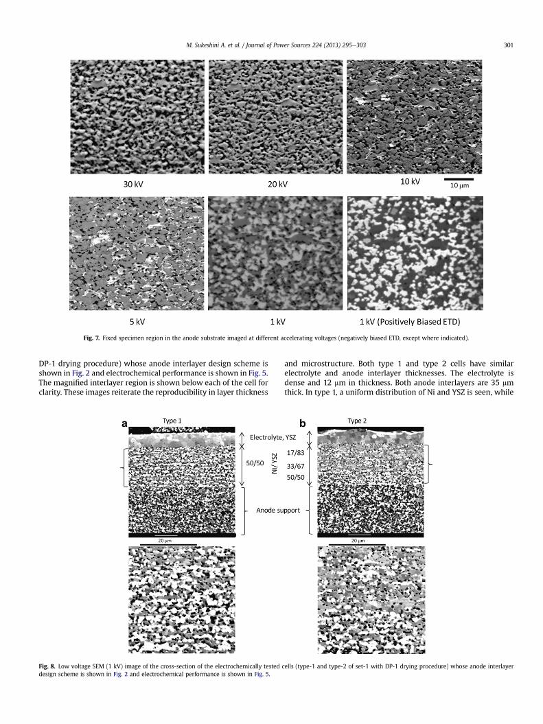
Fig. 7. Fixed specimen region in the anode substrate imaged at different accelerating voltages (negatively biased ETD, except where indicated).
M. Sukeshini A. et al. / Journal of Power Sources 224 (2013) 295e303 301
DP-1 drying procedure) whose anode interlayer design scheme isshown in Fig. 2 and electrochemical performance is shown in Fig. 5.The magnified interlayer region is shown below each of the cell forclarity. These images reiterate the reproducibility in layer thickness
Fig. 8. Low voltage SEM (1 kV) image of the cross-section of the electrochemically tested cdesign scheme is shown in Fig. 2 and electrochemical performance is shown in Fig. 5.
and microstructure. Both type 1 and type 2 cells have similarelectrolyte and anode interlayer thicknesses. The electrolyte isdense and 12 mm in thickness. Both anode interlayers are 35 mmthick. In type 1, a uniform distribution of Ni and YSZ is seen, while
ells (type-1 and type-2 of set-1 with DP-1 drying procedure) whose anode interlayer

M. Sukeshini A. et al. / Journal of Power Sources 224 (2013) 295e303302
a gradation can be readily seen in type 2. On comparing themagnified images of the graded and non-graded layers, it can beseen that the volume fraction of YSZ relative to Ni in the gradedinterlayer is larger in the region adjacent to the electrolytecompared to regions closer to the anode support. The consequentdecrease in ohmic drop in the electrode has likely resulted in theenhanced electrochemical performance. It is also likely that thelesser amount of Ni in the region adjacent to the electrolyte, isbelow the threshold for conductivity based on percolation theory[35]. Typically below this threshold, which is 30 vol%, the cermetexhibits predominantly ionic conducting behavior resulting ina reduction in ohmic resistance in the region adjacent to the elec-trolyte in the graded interlayer that is absent in the non-gradedinterlayer and thus contributes to the enhancement in electro-chemical performance. However, in the non-graded interlayer aswell as the lower region adjacent to the electrolyte in the gradedinterlayer, a layering effect can be seen in the interlayer region, withfeatures similar to striations of Ni and YSZ suggesting eitherinhomogeneous mixing of NiO and YSZ before reaching the depo-sition head or a de-mixing of the two phases on its transit from thedeposition nozzle to the substrate due to differences in density. Thisfactor together with sub optimized layer thickness, porosity andcontiguity likely contribute to the overall less than satisfactoryperformance of the cells. It is also likely that a large part of thenickel is non-percolating. Clearly, further optimization of the anodeinterlayer is required. Optimizations could include, among others,a modification of the thickness of the anode interlayer, quantifyingthe final composition in the interlayer, modifying the viscosities ofthe individual inks and changing the nozzle to substrate distance.Composite cathode layers studied in earlier work [28] presented nomixing/de-mixing issues, and the electrochemical performance ofcells with printed composite cathode showed comparable perfor-mance to those fabricated by slurry pasting. This implies processingand ink optimization issues rather than printing issues. Thispreliminary work on graded composite layers using aerosol jetprinting method shows the potential advantages in terms of elec-trochemical performance of functionally graded anode structuresover non-graded structures. Similar results of performanceenhancement in sub optimized cells have been observed by othergroups, who used graded porosity in tape cast anode supportedcells [36]. Cells with graded anode performed better than cellswithout the graded layer. A power density of 101 mW cm�2 wasobserved for their cells at 600 �C. The results of the current workalso reiterate the reproducibility of component structures andhence electrochemical performance in cells fabricated by directwrite methods. While this preliminary study on compositionalgrading using dual atomizers has provided a platform for fabri-cating functionally graded materials, detailed studies quantifyingthe final compositions etc. are required and will be the topic offuture work.
4. Conclusion
YSZ electrolyte and compositionally graded composite anodeinterlayers were printed by aerosol jet printing from individualcomponents of NiO and YSZ suspensions. The AJP (Aerosol Jet�
Printing) system’s dual atomizer configuration that allows on-demand material mixing was used to deposit the composite NiO/YSZ interlayer component. These electrolyte and anode functionallayers together with a standard LSM (strontium doped lanthanummanganite) based pasted cathode layer were deposited onto anodesupported SOFC button cell. Cells with compositionally gradedanode interlayers performed better than cells with a non-gradedanode interlayer. The enhancement in electrochemical perfor-mance was very consistent and reproducible and can be attributed
to the functional gradation with respect to composition. Themicrostructure in the graded anode interlayer shows a largervolume fraction of YSZ relative to Ni in the region adjacent to theelectrolyte compared to regions closer to the anode support,leading to a reduced ohmic resistance, and hence better electro-chemical performance compared to cells with non graded inter-layer where there is a uniform distribution of Ni and YSZ. However,the overall performance of all cells was not satisfactory, andrequires further optimization of the anode interlayer by altering theink characteristics. Issues relating to improper mixing beforereaching the deposition head or de-mixing of the aerosolizedsuspension on its transit from the nozzle to the substrate requirescloser examination. Low voltage scanning electron microscopy wasused to characterize the printed layers. The use of low acceleratingvoltages (<5 kV) introduces a divergence in the backscatteringcoefficients of YSZ and Ni and enables very clear distinction of thephases, not obtainable with routine scanning electron microscopyusing 10e20 kV. The backscattering mechanism responsible forimage contrast was confirmed and clarified by specially designedSEM experiments that isolated BSE (back scattered electrons) fromSE (secondary electrons).
From the results of the study on microstructural and electro-chemical performance of button cells, it is clear that the currentprinting method of fabricating SOFC layers has advantages of highreproducibility. For SOFC and other applications where componentthicknesses ranging from a few microns to tens of microns, whereboth porous and dense layers are required, and/or complex multi-layer designs such as the segmented in series cells requiring boththickness and spatial control, aerosol jet printing method offersgreat potential as a viable manufacturing method.
Acknowledgments
The authors are greatly appreciative for the assistance ofDr. David Joy of the University of Tennessee at Knoxville and OakRidge National Laboratory for his helpful discussions in regards tounderstanding low-voltage contrast mechanisms and image inter-pretation. Credit is also due to the staff of the Air Force researchlaboratory Materials Characterization Facility for making thespecimen preparations for imaging described in this work.Mr. Thomas Jenkins’ assistance with cell testing is acknowledged.The author, MSA acknowledges Optomec Inc., and the Air ForceResearch Laboratory for the funding, and Dr. Ryan Miller, AFRL forthe facilities and related help.
References
[1] N. Minh, J. Am. Ceram. Soc. 76 (1993) 563e588.[2] S. Singhal, Solid State Ionics 135 (1e4) (2000) 305e313.[3] A.O. Isenberg, Solid State Ionics 3/4 (1981) 431e437.[4] J. Will, A. Mitterdorfer, C. Kleinlogel, D. Perednis, L.J. Gauckler, Solid State
Ionics 131 (1e2) (2000) 79e96.[5] F. Teitz, H.P. Buchkremer, D. Stover, Solid State Ionics 152e153 (2002)
373e381.[6] L.R. Pederson, P. Singh, X.D. Zhou, Vacuum 80 (10) (2006) 1066e1083.[7] A. Negishi, K. Nozaki, T. Ozawa, Solid State Ionics 3/4 (1981) 443.[8] A. Nagata, H. Okayama, Vacuum 66 (2002) 523e529.[9] X. Chen, N.J. Wu, D.L. Ritums, A. Ignatiev, Thin Solid Films 342 (1e2) (1999)
61e66.[10] T. Franco, Z. Hoshiardin, P. Szabo, M. Lang, G. Schiller, J. Fuel Cell. Sci. Technol.
4 (4) (2007) 406e412.[11] G. Schiller, R.H. Henne, M. Lang, R. Ruckdäschel, S. Schaper, Fuel Cells Bull. 3
(21) (2000) 7e12.[12] R. Hui, Z. Wang, O. Kesler, L. Rose, J. Jankovic, S. Yick, R. Maric, D. Ghosh,
J. Power Sources 170 (2007) 308e323.[13] S.C. Singhal, in: S.C. Singhal, M. Dokiya (Eds.), Proc. 6th Int. Symp. Solid Oxide
Fuel Cells (SOFC-VI), The Electrochemical Society, Pennington, NJ, 1999. p. 39.[14] D. Simwonis, H. Thülen, F.J. Dias, A. Naoumidis, D. Stöver, J. Mater. Process.
Technol. 92e93 (1999) 107e111.[15] N. Maffei, G. de Silveira, Solid State Ionics 159 (3e4) (2003) 209e216.

M. Sukeshini A. et al. / Journal of Power Sources 224 (2013) 295e303 303
[16] D. Rotureau, J.-P. Viricelle, C. Pijolat, N. Caillol, M. Pijolat, J. Eur. Ceram. Soc. 25(2005) 2633e2636.
[17] Y. Zhang, J. Gao, G. Meng, X. Lin, J. Appl. Electrochem. 34 (6) (2004) 637e641.[18] E. Schüller, R. Vaßen, D. Stöver, Adv. Eng. Mater. 4 (9) (2002) 659e662.[19] T.W. Kueper, S.J. Visco, L.C. De Jonghe, Solid State Ionics 52 (1992) 251.[20] S. De Souza, S.J. Visco, L.C. De Jonghe, Solid State Ionics 98 (1e2) (1997)
57e61.[21] D. Young, A.M. Sukeshini, R. Cummins, H. Xiao, M. Rottmayer, T. Reitz, J. Power
Sources 184 (2008) 191e196.[22] A.M. El -Toni, T. Yamaguchi, S. Shimizu, Y. Fujishiro, M. Awano, J. Am. Ceram.
Soc. 91 (2008) 346e349.[23] A.M. Sukeshini, R. Cummins, T.L. Reitz, R.M. Miller, Electrochem. Solid-State
Lett. 12 (2009) B176eB179.[24] A.M. Sukeshini, R. Cummins, T.L. Reitz, R.M. Miller, J. Am. Ceram Soc. 92 (12)
(2009) 2913e2919.[25] R.I. Tomov, M. Krauz, J. Jewulski, S.C. Hopkins, J.R. Kluczowski, D.M. Glowacka,
B.A. Glowacki, J. Power Sources 195 (21) (2010) 7160e7167.[26] N. Yashiro, T. Usui, K. Kikuta, J. Eur. Ceram. Soc. 30 (2010) 2093e2098.
[27] A.M. Sukeshini, P. Gardner, T. Jenkins, T.L. Reitz, R.M. Miller, Proceedings of theASME 8th International Conference on Fuel Cell Science, Engineering andTechnology, vol. 1, Brooklyn, NY, 2010, pp. 325e332.
[28] A. Sukeshini, P. Gardner, F. Meisenkothen, T. Jenkins, R. Miller, M. Rottmayer,T.L. Reitz, ECS Trans. 35 (2011) 2151e2160.
[29] http://www.optomec.com.[30] N.T. Hart, N.P. Brandon, M.J. Day, J.E. Shemilt, J. Mater. Sci. 36 (2001) 1077.[31] K. Thydén, Y.L. Liu, J.B. Bilde-Sørensen, Solid State Ionics 178 (39e40) (2008)
1984e1989.[32] J.I. Goldstein, D.E. Newbury, P.E. Echlin, D.C. Joy, A.D. Romig, C.E. Lyman,
C.E. Fiori, E. Lifshin, Scanning Electron Microscopy and X-ray Microanalysis,second ed., Plenum Press, New York, 1992.
[33] D.C. Joy, C.S. Joy, Micron 27 (1996) 247e263.[34] L. Reimer, Image Formation in Low-voltage Scanning Electron Microscopy,
SPIE e The International Society for Optical Engineering, Washington, 1993.[35] D.W. Dees, T.E. Clair, T.E. Easler, D.C. Fee, F.C. Mrazek, J. Electrochem. Soc. 134
(1887) 2141.[36] C.M. An, J.H. Song, I. Kang, N. Sammes, J. Power Sources 195 (3) (2010) 821e824.