
Synthesis of ultrafine single crystals and nanostructured coatings of indium oxide from solution...
8
Applied Surface Science 257 (2011) 6850–6857 Contents lists available at ScienceDirect Applied Surface Science journal homepage: www.elsevier.com/locate/apsusc Synthesis of ultrafine single crystals and nanostructured coatings of indium oxide from solution precursor Nagaswetha Pentyala, Ramesh K. Guduru ∗ , Elizabeth M. Shnerpunas, Pravansu S. Mohanty Department of Mechanical Engineering, University of Michigan, Dearborn, MI 48128, USA article info Article history: Received 15 December 2010 Received in revised form 4 February 2011 Accepted 4 March 2011 Available online 13 March 2011 Keywords: Indium oxide Plasma spray Solution precursor Single crystals Resistivity Optical properties Band gap abstract Indium oxide (In 2 O 3 ) has been widely used in sensors, solar cells and microelectronics. There are several techniques available for making In 2 O 3 such as vapor, electrochemical and atomic layer deposition, which are not only expensive but also time consuming processes. In this study, an inexpensive and straight- forward synthesis approach is being presented to make micron/submicron size single crystals as well as nanostructured adherent coatings of In 2 O 3 using Indium Chloride (InCl 3 ) powders and InCl 3 solution precursor. Both the powders and the solution precursor were calcined in a furnace to obtain the crystals; however, the liquid precursor was also treated by a DC plasma jet to obtain the nanostructured coat- ings. The phase transformations during thermal decomposition of InCl 3 powders and solution precursor were investigated via differential scanning calorimetry studies. The phase structure and crystallinity of the crystals and coatings were confirmed by X-ray diffraction. Microstructural characterization of the crystals and coatings was done by scanning electron microscopy, transmission electron microscopy and atomic force microscopy techniques. Size of the crystals was observed to be dependent on the heating schemes adapted during calcination. Solution precursor plasma sprayed In 2 O 3 coatings showed porosity and ultrafine particulates with grain size ranging between 10 and 75 nm. Resistivity was determined to be ∼0.553 ± 0.337 k cm. Optical transmittance of In 2 O 3 coatings was ∼60–78% in the visible region and it was observed to decrease with increasing the number passes or the thickness of the coatings. Based on the optical transmission data, direct band gap of 3.57 eV was determined. © 2011 Elsevier B.V. All rights reserved. 1. Introduction Indium oxide is an important n-type semiconducting material with a band gap of 3.6 eV [1]. It has received considerable atten- tion among the semiconducting oxides because of its distinctive electrical, optical and chemical properties [2]. Body centered cubic (BCC) In 2 O 3 is very common and it can be used in field emission devices, flat panel displays, biosensing, catalysis, sensors, trans- parent electrodes in solar cells, optics and data storage etc. [3]. Single crystals of BCC–In 2 O 3 are synthesized using chemical vapor deposition (CVD) [4–7], thermal evaporation [8–10] and wet meth- ods [11–13]. Above techniques make use of pure Indium metal or indium based compounds [3–7,14,15] as starting materials. On the other hand, bulk BCC–In 2 O 3 films have been synthesized via spray pyrolysis, magnetron sputtering, electrochemical and vapor deposition techniques [16–19]. Almost all of the above techniques are not only costly with time consuming steps, but also have low throughputs and require expensive starting materials. Therefore, production of In 2 O 3 crystals and coatings directly from simple pre- ∗ Corresponding author. Tel.: +1 313 583 6705; fax: +1 313 593 3851. E-mail address: [email protected] (R.K. Guduru). cursors in a single step with the capability to tailor the structures is of technological and commercial importance. In this study, simple and cost-effective techniques for rapid syn- thesis of both the crystals and the coatings of In 2 O 3 from InCl 3 powders/InCl 3 based solution precursor are reported. The single crystals of BCC–In 2 O 3 were synthesized via furnace calcination of both the InCl 3 powders and the InCl 3 solution precursor, whereas the coatings were developed using a DC plasma spray process with solution precursor of InCl 3 . The furnace calcination technique with- out flow of any gases is not only inexpensive but also easy to control with large throughputs and parameter options, such as time and temperature, and the amount of material to tailor the structures of In 2 O 3 crystals. Also, the production of metal oxide coatings directly from a liquid source in a single step makes liquid precursor plasma spray technique not only a faster process but also attractive for developing nanostructures with an easy control. In the liquid pre- cursor plasma spray, the solution precursor is pumped through high temperature plasma plume where it thermally decomposes into solid nanostructures of desired compound to coat the substrate. Also, this process does not require heating of substrates. In 2 O 3 crystals and coatings were developed via calcination and solution precursor plasma spray technique using InCl 3 precursors, respectively. Thermal conversion of InCl 3 into In 2 O 3 was examined 0169-4332/$ – see front matter © 2011 Elsevier B.V. All rights reserved. doi:10.1016/j.apsusc.2011.03.018
Transcript of Synthesis of ultrafine single crystals and nanostructured coatings of indium oxide from solution...

So
ND
a
ARRAA
KIPSSROB
1
wte(dpSdootsdatp
0d
Applied Surface Science 257 (2011) 6850–6857
Contents lists available at ScienceDirect
Applied Surface Science
journa l homepage: www.e lsev ier .com/ locate /apsusc
ynthesis of ultrafine single crystals and nanostructured coatings of indiumxide from solution precursor
agaswetha Pentyala, Ramesh K. Guduru ∗, Elizabeth M. Shnerpunas, Pravansu S. Mohantyepartment of Mechanical Engineering, University of Michigan, Dearborn, MI 48128, USA
r t i c l e i n f o
rticle history:eceived 15 December 2010eceived in revised form 4 February 2011ccepted 4 March 2011vailable online 13 March 2011
eywords:ndium oxidelasma sprayolution precursoringle crystals
a b s t r a c t
Indium oxide (In2O3) has been widely used in sensors, solar cells and microelectronics. There are severaltechniques available for making In2O3 such as vapor, electrochemical and atomic layer deposition, whichare not only expensive but also time consuming processes. In this study, an inexpensive and straight-forward synthesis approach is being presented to make micron/submicron size single crystals as wellas nanostructured adherent coatings of In2O3 using Indium Chloride (InCl3) powders and InCl3 solutionprecursor. Both the powders and the solution precursor were calcined in a furnace to obtain the crystals;however, the liquid precursor was also treated by a DC plasma jet to obtain the nanostructured coat-ings. The phase transformations during thermal decomposition of InCl3 powders and solution precursorwere investigated via differential scanning calorimetry studies. The phase structure and crystallinity ofthe crystals and coatings were confirmed by X-ray diffraction. Microstructural characterization of the
esistivityptical propertiesand gap
crystals and coatings was done by scanning electron microscopy, transmission electron microscopy andatomic force microscopy techniques. Size of the crystals was observed to be dependent on the heatingschemes adapted during calcination. Solution precursor plasma sprayed In2O3 coatings showed porosityand ultrafine particulates with grain size ranging between 10 and 75 nm. Resistivity was determined tobe ∼0.553 ± 0.337 k� cm. Optical transmittance of In2O3 coatings was ∼60–78% in the visible region andit was observed to decrease with increasing the number passes or the thickness of the coatings. Based on
ata,
the optical transmission d. Introduction
Indium oxide is an important n-type semiconducting materialith a band gap of 3.6 eV [1]. It has received considerable atten-
ion among the semiconducting oxides because of its distinctivelectrical, optical and chemical properties [2]. Body centered cubicBCC) In2O3 is very common and it can be used in field emissionevices, flat panel displays, biosensing, catalysis, sensors, trans-arent electrodes in solar cells, optics and data storage etc. [3].ingle crystals of BCC–In2O3 are synthesized using chemical vaporeposition (CVD) [4–7], thermal evaporation [8–10] and wet meth-ds [11–13]. Above techniques make use of pure Indium metalr indium based compounds [3–7,14,15] as starting materials. Onhe other hand, bulk BCC–In2O3 films have been synthesized viapray pyrolysis, magnetron sputtering, electrochemical and vapor
eposition techniques [16–19]. Almost all of the above techniquesre not only costly with time consuming steps, but also have lowhroughputs and require expensive starting materials. Therefore,roduction of In2O3 crystals and coatings directly from simple pre-∗ Corresponding author. Tel.: +1 313 583 6705; fax: +1 313 593 3851.E-mail address: [email protected] (R.K. Guduru).
169-4332/$ – see front matter © 2011 Elsevier B.V. All rights reserved.oi:10.1016/j.apsusc.2011.03.018
direct band gap of 3.57 eV was determined.© 2011 Elsevier B.V. All rights reserved.
cursors in a single step with the capability to tailor the structuresis of technological and commercial importance.
In this study, simple and cost-effective techniques for rapid syn-thesis of both the crystals and the coatings of In2O3 from InCl3powders/InCl3 based solution precursor are reported. The singlecrystals of BCC–In2O3 were synthesized via furnace calcination ofboth the InCl3 powders and the InCl3 solution precursor, whereasthe coatings were developed using a DC plasma spray process withsolution precursor of InCl3. The furnace calcination technique with-out flow of any gases is not only inexpensive but also easy to controlwith large throughputs and parameter options, such as time andtemperature, and the amount of material to tailor the structures ofIn2O3 crystals. Also, the production of metal oxide coatings directlyfrom a liquid source in a single step makes liquid precursor plasmaspray technique not only a faster process but also attractive fordeveloping nanostructures with an easy control. In the liquid pre-cursor plasma spray, the solution precursor is pumped through hightemperature plasma plume where it thermally decomposes into
solid nanostructures of desired compound to coat the substrate.Also, this process does not require heating of substrates.In2O3 crystals and coatings were developed via calcination andsolution precursor plasma spray technique using InCl3 precursors,respectively. Thermal conversion of InCl3 into In2O3 was examined
N. Pentyala et al. / Applied Surface Sc
FP
vwto
2
2
I2stip
2
anAcase
2
II3tvstippaoppacs[
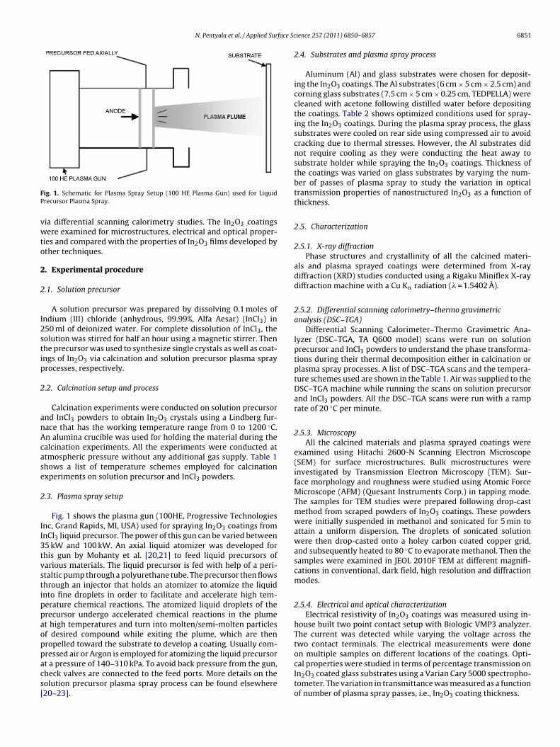
ig. 1. Schematic for Plasma Spray Setup (100 HE Plasma Gun) used for Liquidrecursor Plasma Spray.
ia differential scanning calorimetry studies. The In2O3 coatingsere examined for microstructures, electrical and optical proper-
ies and compared with the properties of In2O3 films developed byther techniques.
. Experimental procedure
.1. Solution precursor
A solution precursor was prepared by dissolving 0.1 moles ofndium (III) chloride (anhydrous, 99.99%, Alfa Aesar) (InCl3) in50 ml of deionized water. For complete dissolution of InCl3, theolution was stirred for half an hour using a magnetic stirrer. Thenhe precursor was used to synthesize single crystals as well as coat-ngs of In2O3 via calcination and solution precursor plasma sprayrocesses, respectively.
.2. Calcination setup and process
Calcination experiments were conducted on solution precursornd InCl3 powders to obtain In2O3 crystals using a Lindberg fur-ace that has the working temperature range from 0 to 1200 ◦C.n alumina crucible was used for holding the material during thealcination experiments. All the experiments were conducted attmospheric pressure without any additional gas supply. Table 1hows a list of temperature schemes employed for calcinationxperiments on solution precursor and InCl3 powders.
.3. Plasma spray setup
Fig. 1 shows the plasma gun (100HE, Progressive Technologiesnc, Grand Rapids, MI, USA) used for spraying In2O3 coatings fromnCl3 liquid precursor. The power of this gun can be varied between5 kW and 100 kW. An axial liquid atomizer was developed forhis gun by Mohanty et al. [20,21] to feed liquid precursors ofarious materials. The liquid precursor is fed with help of a peri-taltic pump through a polyurethane tube. The precursor then flowshrough an injector that holds an atomizer to atomize the liquidnto fine droplets in order to facilitate and accelerate high tem-erature chemical reactions. The atomized liquid droplets of therecursor undergo accelerated chemical reactions in the plumet high temperatures and turn into molten/semi-molten particlesf desired compound while exiting the plume, which are thenropelled toward the substrate to develop a coating. Usually com-
ressed air or Argon is employed for atomizing the liquid precursort a pressure of 140–310 kPa. To avoid back pressure from the gun,heck valves are connected to the feed ports. More details on theolution precursor plasma spray process can be found elsewhere20–23].ience 257 (2011) 6850–6857 6851
2.4. Substrates and plasma spray process
Aluminum (Al) and glass substrates were chosen for deposit-ing the In2O3 coatings. The Al substrates (6 cm × 5 cm × 2.5 cm) andcorning glass substrates (7.5 cm × 5 cm × 0.25 cm, TEDPELLA) werecleaned with acetone following distilled water before depositingthe coatings. Table 2 shows optimized conditions used for spray-ing the In2O3 coatings. During the plasma spray process, the glasssubstrates were cooled on rear side using compressed air to avoidcracking due to thermal stresses. However, the Al substrates didnot require cooling as they were conducting the heat away tosubstrate holder while spraying the In2O3 coatings. Thickness ofthe coatings was varied on glass substrates by varying the num-ber of passes of plasma spray to study the variation in opticaltransmission properties of nanostructured In2O3 as a function ofthickness.
2.5. Characterization
2.5.1. X-ray diffractionPhase structures and crystallinity of all the calcined materi-
als and plasma sprayed coatings were determined from X-raydiffraction (XRD) studies conducted using a Rigaku Miniflex X-raydiffraction machine with a Cu K� radiation (� = 1.5402 A).
2.5.2. Differential scanning calorimetry–thermo gravimetricanalysis (DSC–TGA)
Differential Scanning Calorimeter–Thermo Gravimetric Ana-lyzer (DSC–TGA, TA Q600 model) scans were run on solutionprecursor and InCl3 powders to understand the phase transforma-tions during their thermal decomposition either in calcination orplasma spray processes. A list of DSC–TGA scans and the tempera-ture schemes used are shown in the Table 1. Air was supplied to theDSC–TGA machine while running the scans on solution precursorand InCl3 powders. All the DSC–TGA scans were run with a ramprate of 20 ◦C per minute.
2.5.3. MicroscopyAll the calcined materials and plasma sprayed coatings were
examined using Hitachi 2600-N Scanning Electron Microscope(SEM) for surface microstructures. Bulk microstructures wereinvestigated by Transmission Electron Microscopy (TEM). Sur-face morphology and roughness were studied using Atomic ForceMicroscope (AFM) (Quesant Instruments Corp.) in tapping mode.The samples for TEM studies were prepared following drop-castmethod from scraped powders of In2O3 coatings. These powderswere initially suspended in methanol and sonicated for 5 min toattain a uniform dispersion. The droplets of sonicated solutionwere then drop-casted onto a holey carbon coated copper grid,and subsequently heated to 80 ◦C to evaporate methanol. Then thesamples were examined in JEOL 2010F TEM at different magnifi-cations in conventional, dark field, high resolution and diffractionmodes.
2.5.4. Electrical and optical characterizationElectrical resistivity of In2O3 coatings was measured using in-
house built two point contact setup with Biologic VMP3 analyzer.The current was detected while varying the voltage across thetwo contact terminals. The electrical measurements were done
on multiple samples on different locations of the coatings. Opti-cal properties were studied in terms of percentage transmission onIn2O3 coated glass substrates using a Varian Cary 5000 spectropho-tometer. The variation in transmittance was measured as a functionof number of plasma spray passes, i.e., In2O3 coating thickness.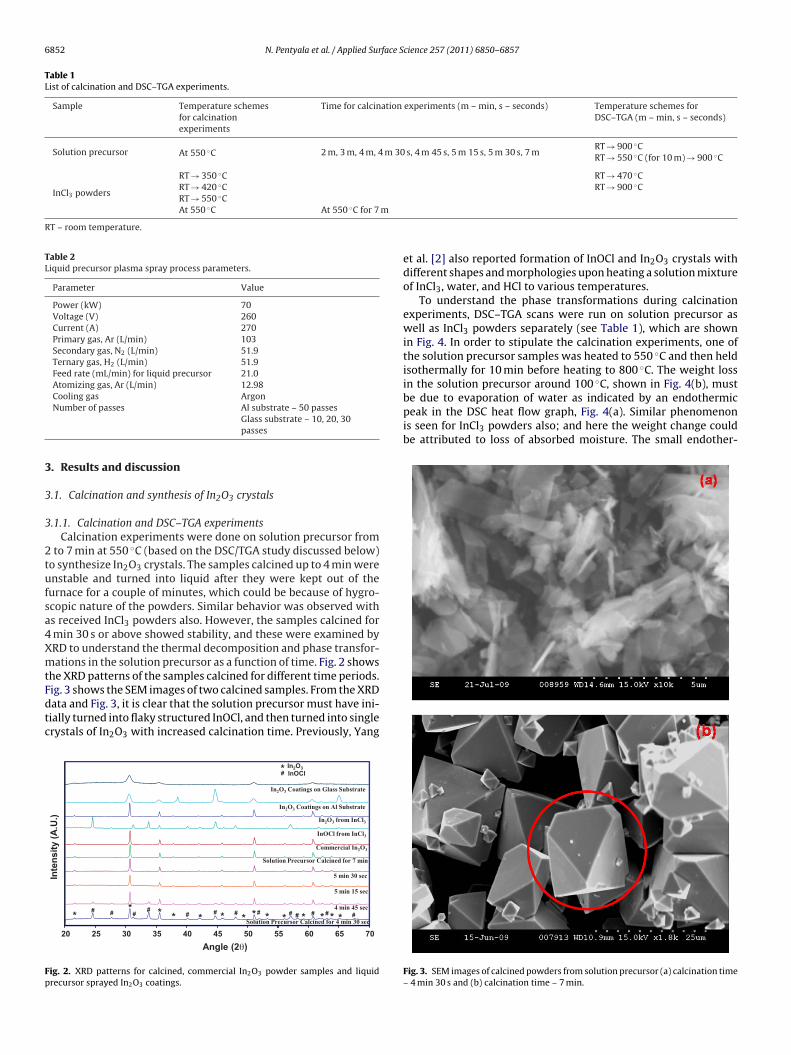
6852 N. Pentyala et al. / Applied Surface Science 257 (2011) 6850–6857
Table 1List of calcination and DSC–TGA experiments.
Sample Temperature schemesfor calcinationexperiments
Time for calcination experiments (m – min, s – seconds) Temperature schemes forDSC–TGA (m – min, s – seconds)
Solution precursor At 550 ◦C 2 m, 3 m, 4 m, 4 m 30 s, 4 m 45 s, 5 m 15 s, 5 m 30 s, 7 mRT → 900 ◦CRT → 550 ◦C (for 10 m) → 900 ◦C
InCl3 powders
RT → 350 ◦C RT → 470 ◦CRT → 420 ◦C RT → 900 ◦CRT → 550 ◦CAt 550 ◦C At 550 ◦C for 7 m
RT – room temperature.
Table 2Liquid precursor plasma spray process parameters.
Parameter Value
Power (kW) 70Voltage (V) 260Current (A) 270Primary gas, Ar (L/min) 103Secondary gas, N2 (L/min) 51.9Ternary gas, H2 (L/min) 51.9Feed rate (mL/min) for liquid precursor 21.0Atomizing gas, Ar (L/min) 12.98Cooling gas Argon
3
3
3
2tufsa4XmtFdtc
Fp
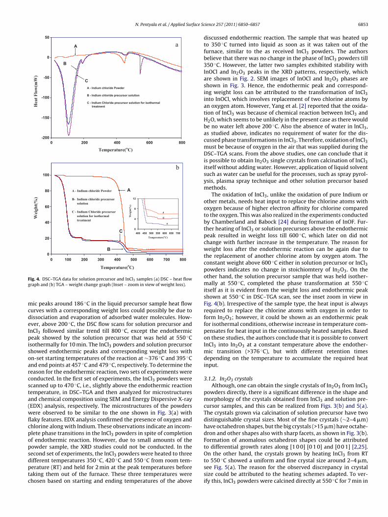
in the solution precursor around 100 ◦C, shown in Fig. 4(b), mustbe due to evaporation of water as indicated by an endothermicpeak in the DSC heat flow graph, Fig. 4(a). Similar phenomenonis seen for InCl3 powders also; and here the weight change couldbe attributed to loss of absorbed moisture. The small endother-
Number of passes Al substrate – 50 passesGlass substrate – 10, 20, 30passes
. Results and discussion
.1. Calcination and synthesis of In2O3 crystals
.1.1. Calcination and DSC–TGA experimentsCalcination experiments were done on solution precursor from
to 7 min at 550 ◦C (based on the DSC/TGA study discussed below)o synthesize In2O3 crystals. The samples calcined up to 4 min werenstable and turned into liquid after they were kept out of theurnace for a couple of minutes, which could be because of hygro-copic nature of the powders. Similar behavior was observed withs received InCl3 powders also. However, the samples calcined formin 30 s or above showed stability, and these were examined byRD to understand the thermal decomposition and phase transfor-ations in the solution precursor as a function of time. Fig. 2 shows
he XRD patterns of the samples calcined for different time periods.ig. 3 shows the SEM images of two calcined samples. From the XRData and Fig. 3, it is clear that the solution precursor must have ini-ially turned into flaky structured InOCl, and then turned into singlerystals of In2O3 with increased calcination time. Previously, Yang
7065605550454035302520
Inte
nsity
(A.U
.)
Angle (2θ)
*
ig. 2. XRD patterns for calcined, commercial In2O3 powder samples and liquidrecursor sprayed In2O3 coatings.
et al. [2] also reported formation of InOCl and In2O3 crystals withdifferent shapes and morphologies upon heating a solution mixtureof InCl3, water, and HCl to various temperatures.
To understand the phase transformations during calcinationexperiments, DSC–TGA scans were run on solution precursor aswell as InCl3 powders separately (see Table 1), which are shownin Fig. 4. In order to stipulate the calcination experiments, one ofthe solution precursor samples was heated to 550 ◦C and then heldisothermally for 10 min before heating to 800 ◦C. The weight loss
Fig. 3. SEM images of calcined powders from solution precursor (a) calcination time– 4 min 30 s and (b) calcination time – 7 min.
N. Pentyala et al. / Applied Surface Sc
-200
-150
-100
-50
0
50
8006004002000
Temperature(oC)
Hea
t F
low
(mW
)
A - Indium chloride Powder
B - Indium chloride precursor solution
C - Indium Chloride precursor solution for isothermal treatment
A
B
C
a
0
20
40
60
80
100
8007006005004003002001000
Temperature(oC)
Wei
gh
t(%
)
A - Indium chloride Powder
B- Indium chloride precursor
solution
C - Indium Chloride precursor
solution for isothermal
treatment
C
B
b
Fg
mcdeIpisoarcsta(wflcpopsdptc
On the other hand, the crystals grown by heating InCl3 from RT
ig. 4. DSC–TGA data for solution precursor and InCl3 samples (a) DSC – heat flowraph and (b) TGA – weight change graph (Inset – zoom in view of weight loss).
ic peaks around 186 ◦C in the liquid precursor sample heat flowurves with a corresponding weight loss could possibly be due toissociation and evaporation of adsorbed water molecules. How-ver, above 200 ◦C, the DSC flow scans for solution precursor andnCl3 followed similar trend till 800 ◦C, except the endothermiceak showed by the solution precursor that was held at 550 ◦C
sothermally for 10 min. The InCl3 powders and solution precursorhowed endothermic peaks and corresponding weight loss withn-set starting temperatures of the reaction at ∼376 ◦C and 395 ◦Cnd end points at 457 ◦C and 479 ◦C, respectively. To determine theeason for the endothermic reaction, two sets of experiments wereonducted. In the first set of experiments, the InCl3 powders werecanned up to 470 ◦C, i.e., slightly above the endothermic reactionemperature, in DSC–TGA and then analyzed for microstructuresnd chemical composition using SEM and Energy Dispersive X-rayEDX) analysis, respectively. The microstructures of the powdersere observed to be similar to the one shown in Fig. 3(a) withaky features. EDX analysis confirmed the presence of oxygen andhlorine along with Indium. These observations indicate an incom-lete phase transitions in the InCl3 powders in spite of completionf endothermic reaction. However, due to small amounts of theowder sample, the XRD studies could not be conducted. In theecond set of experiments, the InCl3 powders were heated to three
ifferent temperatures 350 ◦C, 420 ◦C and 550 ◦C from room tem-erature (RT) and held for 2 min at the peak temperatures beforeaking them out of the furnace. These three temperatures werehosen based on starting and ending temperatures of the aboveience 257 (2011) 6850–6857 6853
discussed endothermic reaction. The sample that was heated upto 350 ◦C turned into liquid as soon as it was taken out of thefurnace, similar to the as received InCl3 powders. The authorsbelieve that there was no change in the phase of InCl3 powders till350 ◦C. However, the latter two samples exhibited stability withInOCl and In2O3 peaks in the XRD patterns, respectively, whichare shown in Fig. 2. SEM images of InOCl and In2O3 phases areshown in Fig. 3. Hence, the endothermic peak and correspond-ing weight loss can be attributed to the transformation of InCl3into InOCl, which involves replacement of two chlorine atoms byan oxygen atom. However, Yang et al. [2] reported that the oxida-tion of InCl3 was because of chemical reaction between InCl3 andH2O, which seems to be unlikely in the present case as there wouldbe no water left above 200 ◦C. Also the absence of water in InCl3,as studied above, indicates no requirement of water for the dis-cussed phase transformations in InCl3. Therefore, oxidation of InCl3must be because of oxygen in the air that was supplied during theDSC–TGA scans. From the above studies, one can conclude that itis possible to obtain In2O3 single crystals from calcination of InCl3itself without adding water. However, application of liquid solventsuch as water can be useful for the processes, such as spray pyrol-ysis, plasma spray technique and other solution precursor basedmethods.
The oxidation of InCl3, unlike the oxidation of pure Indium orother metals, needs heat input to replace the chlorine atoms withoxygen because of higher electron affinity for chlorine comparedto the oxygen. This was also realized in the experiments conductedby Chamberland and Babock [24] during formation of InOF. Fur-ther heating of InCl3 or solution precursors above the endothermicpeak resulted in weight loss till 600 ◦C, which later on did notchange with further increase in the temperature. The reason forweight loss after the endothermic reaction can be again due tothe replacement of another chlorine atom by oxygen atom. Theconstant weight above 600 ◦C either in solution precursor or InCl3powders indicates no change in stoichiomtery of In2O3. On theother hand, the solution precursor sample that was held isother-mally at 550 ◦C, completed the phase transformation at 550 ◦Citself as it is evident from the weight loss and endothermic peakshown at 550 ◦C in DSC–TGA scan, see the inset zoom in view inFig. 4(b). Irrespective of the sample type, the heat input is alwaysrequired to replace the chlorine atoms with oxygen in order toform In2O3; however, it could be shown as an endothermic peakfor isothermal conditions, otherwise increase in temperature com-pensates for heat input in the continuously heated samples. Basedon these studies, the authors conclude that it is possible to convertInCl3 into In2O3 at a constant temperature above the endother-mic transition (>376 ◦C), but with different retention timesdepending on the temperature to accumulate the required heatinput.
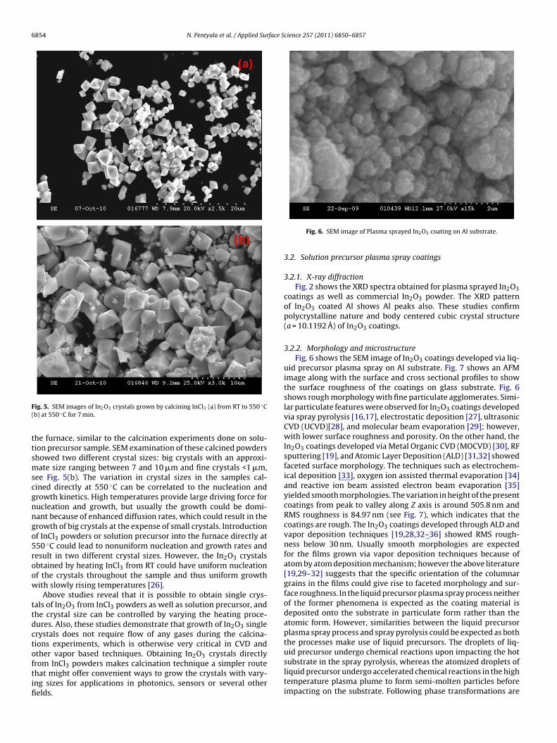
3.1.2. In2O3 crystalsAlthough, one can obtain the single crystals of In2O3 from InCl3
powders directly, there is a significant difference in the shape andmorphology of the crystals obtained from InCl3 and solution pre-cursor samples, and this can be realized from Figs. 3(b) and 5(a).The crystals grown via calcination of solution precursor have twodistinguishable crystal sizes. Most of the fine crystals (∼2–4 �m)have octahedron shapes, but the big crystals (>15 �m) have octahe-dron and other shapes also with sharp facets, as shown in Fig. 3(b).Formation of anomalous octahedron shapes could be attributedto differential growth rates along [1 0 0] [0 1 0] and [0 0 1] [2,25].
to 550 ◦C showed a uniform and fine crystal size around 2–4 �m,see Fig. 5(a). The reason for the observed discrepancy in crystalsize could be attributed to the heating schemes adapted. To ver-ify this, InCl3 powders were calcined directly at 550 ◦C for 7 min in
6854 N. Pentyala et al. / Applied Surface Science 257 (2011) 6850–6857
F(
ttsmscgnngo5roow
ttdctoftifi
uid precursor undergo chemical reactions upon impacting the hot
ig. 5. SEM images of In2O3 crystals grown by calcining InCl3 (a) from RT to 550 ◦Cb) at 550 ◦C for 7 min.
he furnace, similar to the calcination experiments done on solu-ion precursor sample. SEM examination of these calcined powdershowed two different crystal sizes: big crystals with an approxi-ate size ranging between 7 and 10 �m and fine crystals <1 �m,
ee Fig. 5(b). The variation in crystal sizes in the samples cal-ined directly at 550 ◦C can be correlated to the nucleation androwth kinetics. High temperatures provide large driving force forucleation and growth, but usually the growth could be domi-ant because of enhanced diffusion rates, which could result in therowth of big crystals at the expense of small crystals. Introductionf InCl3 powders or solution precursor into the furnace directly at50 ◦C could lead to nonuniform nucleation and growth rates andesult in two different crystal sizes. However, the In2O3 crystalsbtained by heating InCl3 from RT could have uniform nucleationf the crystals throughout the sample and thus uniform growthith slowly rising temperatures [26].
Above studies reveal that it is possible to obtain single crys-als of In2O3 from InCl3 powders as well as solution precursor, andhe crystal size can be controlled by varying the heating proce-ures. Also, these studies demonstrate that growth of In2O3 singlerystals does not require flow of any gases during the calcina-ions experiments, which is otherwise very critical in CVD andther vapor based techniques. Obtaining In O crystals directly
2 3rom InCl3 powders makes calcination technique a simpler routehat might offer convenient ways to grow the crystals with vary-ng sizes for applications in photonics, sensors or several otherelds.Fig. 6. SEM image of Plasma sprayed In2O3 coating on Al substrate.
3.2. Solution precursor plasma spray coatings
3.2.1. X-ray diffractionFig. 2 shows the XRD spectra obtained for plasma sprayed In2O3
coatings as well as commercial In2O3 powder. The XRD patternof In2O3 coated Al shows Al peaks also. These studies confirmpolycrystalline nature and body centered cubic crystal structure(a = 10.1192 A) of In2O3 coatings.
3.2.2. Morphology and microstructureFig. 6 shows the SEM image of In2O3 coatings developed via liq-
uid precursor plasma spray on Al substrate. Fig. 7 shows an AFMimage along with the surface and cross sectional profiles to showthe surface roughness of the coatings on glass substrate. Fig. 6shows rough morphology with fine particulate agglomerates. Simi-lar particulate features were observed for In2O3 coatings developedvia spray pyrolysis [16,17], electrostatic deposition [27], ultrasonicCVD (UCVD)[28], and molecular beam evaporation [29]; however,with lower surface roughness and porosity. On the other hand, theIn2O3 coatings developed via Metal Organic CVD (MOCVD) [30], RFsputtering [19], and Atomic Layer Deposition (ALD) [31,32] showedfaceted surface morphology. The techniques such as electrochem-ical deposition [33], oxygen ion assisted thermal evaporation [34]and reactive ion beam assisted electron beam evaporation [35]yielded smooth morphologies. The variation in height of the presentcoatings from peak to valley along Z axis is around 505.8 nm andRMS roughness is 84.97 nm (see Fig. 7), which indicates that thecoatings are rough. The In2O3 coatings developed through ALD andvapor deposition techniques [19,28,32–36] showed RMS rough-ness below 30 nm. Usually smooth morphologies are expectedfor the films grown via vapor deposition techniques because ofatom by atom deposition mechanism; however the above literature[19,29–32] suggests that the specific orientation of the columnargrains in the films could give rise to faceted morphology and sur-face roughness. In the liquid precursor plasma spray process neitherof the former phenomena is expected as the coating material isdeposited onto the substrate in particulate form rather than theatomic form. However, similarities between the liquid precursorplasma spray process and spray pyrolysis could be expected as boththe processes make use of liquid precursors. The droplets of liq-
substrate in the spray pyrolysis, whereas the atomized droplets ofliquid precursor undergo accelerated chemical reactions in the hightemperature plasma plume to form semi-molten particles beforeimpacting on the substrate. Following phase transformations are

N. Pentyala et al. / Applied Surface Science 257 (2011) 6850–6857 6855
urface
ectp
I
TsdbstFtrip
wasrooedTdviaSvP
Fig. 7. AFM image of In2O3 coating (a) 3D-view of 4 �m × 4 �m, (b) S
xpected to occur during the thermal decomposition of liquid pre-ursor in the plasma plume at very fast rates due to small size ofhe atomized liquid droplets as well as high temperatures of thelasma plume [3,16,35]:
nCl3 → InOCl → In2O3 (1)
he liquid precursor plasma spray process is advantageous overpray pyrolysis because of rapid production of coatings as well as itoes not require preheating of the substrates. For example, it coulde very useful for spraying coatings on low melting or polymerubstrates. In addition, plasma spray process can yield fine struc-ures by tailoring the extent of atomization of the liquid precursor.igs. 6 and 7 show nano particulate agglomerates of In2O3. Forma-ion of agglomerates could be attributed to high temperatures andapid quenching in the plasma plume. The particles formed dur-ng thermal decomposition of the atomized liquid droplets couldossibly fuse together into agglomerates before exiting the plume.
Microstructures of the agglomerates and ultrafine particulatesere examined in TEM. Fig. 8(a) shows the TEM image of In2O3
gglomerates with very fine grain size. The diffraction pattern,hown in the inset, confirmed the crystal structure of In2O3. Highesolution image shown in Fig. 8(b) indicates an interplanar spacingf 0.29 nm between two consecutive (2 2 2) planes of BCC structuref In2O3. It is evident from the TEM image that the coating hasquiaxed grains with few tens of nanometers in size. Grain sizeistribution for In2O3 coatings is shown in the inset of Fig. 8(a).he grain size measurements were done using several bright andark field images with line intercept method. A total of 237 indi-idual grains were considered for the Gaussian distribution shown
n the inset of Fig. 8(a). The grain size varied between 10 and 80 nmnd average grain size was calculated to be approximately 33.4 nm.imilar grain sizes were reported in the In2O3 coatings developedia spray pyrolysis, oxygen ion assisted thermal evaporation, ALD,ulsed Laser Deposition (PLD), CVD coatings [3,17,31,32,36,37]. Theprofile and (c) Cross sectional view for the dotted line shown in (b).
grain size of sol–gel coatings was smaller than these coatings andvaried from 10 nm to 20 nm [38,39]. On the other hand, the grainsize for sputtering, UCVD, molecular beam evaporation, electronbeam deposition coatings was reported to be greater than 100 nm[28,29,40,41]. The grain size of vapor deposited coatings is usuallydependent on the thickness of the coatings. In the present coat-ings, it is influenced by the extent of atomization, i.e., size of theatomized liquid droplets as well as quench rates in the liquid pre-cursor plasma spray process. Finer the liquid droplet size, finerwould be the grain size because of lesser mass of the transformedsemi-molten or molten solid phase particle which undergoes rapidquenching upon exiting the plasma plume. However, the quenchrates are also dependent on the substrate temperatures. Preheat-ing or continuous cooling of the substrates can lead to either slowor rapid quenching of the substrates as well as the coatings. Highquench rates either result in fine grain size or sometimes amor-phous structures depending on the material being sprayed. Theextent of atomization and quenching can be varied to obtain desiredgrain size and microstructures in the solution precursor plasmasprayed coatings by varying the spray parameters. Also, the amountof porosity can be tailored by plasma parameter optimization. Largeamount of porosity of the present coatings with nano structures andrough morphology as shown in Figs. 6 and 7 could provide largesurface area that could be useful in sensing applications.
3.3. Electrical measurements
Due to the porous nature of the In2O3 coatings a hemisphericalprobe was used with large area of contact for electrical mea-
surements. During electrical characterization, the current passedthrough the coatings was varied and then voltage was detectedacross the contact terminals. Fig. 9 shows an exemplary graphbetween current (I) and voltage (V) for electrical measurementsdone on one of the In2O3 coatings sprayed on Al substrates in
6856 N. Pentyala et al. / Applied Surface Science 257 (2011) 6850–6857
Fig. 8. (a) Bright field TEM image of Plasma sprayed In2O3 coating (Inset – grain size distribution (top) diffraction pattern (bottom)). (b) HRTEM image of Plasma sprayedIn2O3 coating.
0
0.01
0.02
0.03
0.04
0.00050.00040.00030.00020.00010
Vo
lta
ge(
V)
ρ =.553 ± 0.337KΩ-cm
Fo
atv10tcpsIu
3
emfncl(
Fig. 10. Optical transmittance of In O coatings with different number of plasma
Current (A)
ig. 9. Electrical measurements: current (I) vs. voltage (V) graph for In2O3 coatingn Al substrate using two point probe analyzer.
s deposited condition. Slope of the I − V graph indicates resis-ance of the coating between two terminals that measured theoltage across. However, using the coating thickness, which was0.8 �m for 30 passes sample, the resistivity was determined to be.553 ± 0.337 k� cm. The resistivity of In2O3 coatings was reportedo be ∼10−4 � cm in the literature [42–46]. The resistivity of presentoatings is very high and it could be attributed to porosity andarticulate nature of the coatings. The scatter in electrical mea-urements is also an indication for the same. The conductivity ofn2O3 is dependent on the number of oxygen ion vacancies, andsually more the vacancies better will be the conductivity [46–48].
.4. Optical properties
The transmission spectra for different thicknesses of In2O3 lay-rs sprayed on Corning glass substrates are shown in Fig. 10. Theaximum transmittance (%T) was observed to be around 60–78%
or ten passes sample, however, it decreased with increasing theumber of passes, i.e., with increasing the thickness of In2O3oatings. The transmittance of present coatings is comparable orower than the transmittance of In2O3 coatings developed via ALD80–90%) [31,32], reactive ion beam assisted electron beam evap-
2 3
spray passes, i.e., thickness (Inset – optical direct band gap for In2O3 coating – 10passes sample (coating thickness – 3.3 �m)).
oration (80%) [35], MOCVD (80%) [49], reactive electron Beamevaporation (85%) [45], reactive ion beam assisted deposition (80%)[35], spray pyrolysis (90%) [50]. Oxygen ion beam assisted depo-sition (94%) [44], thermal evaporation under high vacuum (>75%)[43]. However, it is slightly higher than the spray pyrolysis coatingsdeposited at 500 ◦C (∼65%) [17], and PLD films (<40%) [38]. Accord-ing to the literature [51–53] the transmission of In2O3 coatings isnot only dependent on the surface morphology, porosity but alsothe crystallinity and oxygen vacancies. Discontinuous grain growthor finer grain sizes were attributed to cause light scattering and thusreduced transmission [38]. Improved crystallinity after anneal-ing treatment, as well as increased oxygen incorporation into thecoatings with improved stoichiomtery was observed to enhancethe transmittance [54,55]. Thilakan and Kumar [56] reported theeffect of orientation of In2O3 films also on their transmittance. Thepresent coatings are polycrystalline in nature with random orien-tation of the grains. Added to that, porosity and roughness withparticulate nature of the coatings could reduce the transmittance.With increased number of passes, the defects, such as porosity and
particulate boundaries are also expected to increase. Therefore,decrease in transmittance with increasing the coating thicknesscould be attributed to internal scattering of the light within thecoating due to the above mentioned defects.
face Sc
dotcfif
T
we
˛
w(lts2db˛aca
4
capwueOasmInoiucdvsn
A
h
R
[
[
[
[[
[[
[
[[[
[[
[
[[[
[[[[[
[[[[
[[[
[
[
[[
[
[[
[
[[[[
[
[[
[[
N. Pentyala et al. / Applied Sur
Nevertheless, the electron excitation from valence band to con-uction band occurs only when the photon energy is equivalent tor higher than the band gap of In2O3 [57,58]. Therefore, decreasedransmittance because of increased absorbance around 300 nmould be correlated to the band gap of In2O3. The absorption coef-cient (˛) was calculated from transmittance (T) data using the
ollowing equation [38]
= exp(−˛t) (2)
here t is the thickness of the film. The optical band gap Eg wasstimated from the following relation known as the Tauc plot [59]
h� = A(h� − Eg)n (3)
here A is the band edge constant, h is the Planck’s constant6.626 × 10−34 J s), � is the frequency of photons (� = speed ofight/wavelength of the photon), and the exponent n characterizeshe nature of band transition. The values 1/2 and 3/2 for ‘n’ corre-pond to direct allowed and direct forbidden transitions, whereas
and 3 correspond to the indirect allowed and indirect forbid-en transitions, respectively. The band gap energy was obtainedy extrapolating the straight line portion of (˛h�)1/n vs. h� plot toh� = 0. Inset of Fig. 10 shows a band gap of ∼3.57 eV for directllowed transitions and it was observed to be independent of theoating thickness. The band gap value is comparable with the liter-ture [38].
. Conclusions
Single crystals and nanostructured coatings of In2O3 were suc-essfully developed using InCl3 based precursors via calcinationnd DC plasma spray techniques, respectively. The thermal decom-osition behavior and phase transformations in InCl3 precursorsere investigated via DSC–TGA scans and the InCl3 was observed tondergo phase transition into InOCl before turning into In2O3 withndothermic reactions to replace the chlorine atoms with oxygen.xidation behavior of InCl3 indicated requirement of air/oxygenlone without water, unlike it was reported in the literature. Theize of In2O3 crystals was observed to vary with the thermal treat-ents adapted in the calcination experiments. Microstructures of
n2O3 coatings revealed porous agglomerates and particulates withanostructures. The optical transmittance of In2O3 coatings wasbserved to decrease with increasing the coating thickness due toncreased particulate boundaries and other surface defects, yet withnaffected band gap with respect to the thickness. Inexpensive andontrolled growth of single crystals of In2O3 via calcination route,irectly from InCl3 powders, could be of commercial interest forarious applications. Alternatively, the In2O3 coatings with largeurface area due to porosity, ultrafine particulate boundaries andanostructures could find applications in sensors.
cknowledgements
The authors would like to thank Raghavender Tummala for hiselp in thermal spray process.
eferences
[1] Y.Ch. Wang, Y. Dai, J. Pezoldt, B. Lu, Th. Kups, V. Cimalla, O. Ambacher, Cryst.Growth Des. 8 (4) (2008) 1257.
[2] H. Yang, H. Zhao, H. Dong, W. Yang, D. Chen, Mater. Res. Bull. 44 (2009) 1148.[3] W. Yin, M. Cao, S. Luo, C. Hu, B. Wei, Cryst. Growth Des. 9 (5) (2009) 2173.[4] J. Lao, J. Huang, D. Wang, Z. Ren, Adv. Mater. 16 (1) (2004) 65.
[[[
[
ience 257 (2011) 6850–6857 6857
[5] C. Liang, G. Meng, Y. Lei, F. Phillipp, L. Zhang, Adv. Mater. 13 (17) (2001) 1330.[6] J.S. Jeong, J.Y. Lee, C.J. Lee, S.J. An, G.-C. Yi, Chem. Phys. Lett. 384 (2004) 246.[7] Y. Hao, G. Meng, C. Ye, L. Zhang, Cryst. Growth Des. 5 (4) (2005) 1617.[8] Z.W. Pan, Z.R. Dai, Z.L. Wang, Science 291 (2001) 1947.[9] Y. Li, Y. Bando, D. Golberg, Adv. Mater. 15 (2003) 581.10] H. Lorenz, M. Stoger-Pollach, S. Schwarz, K. Pfaller, B. Klotzer, J. Bernardi, S.
Penner, J. Phys. Chem. C 112 (2008) 918.11] A. Gurlo, N. Barsan, U. Weimar, M. Ivanovskaya, A. Taurino, P. Siciliano, Chem.
Mater. 15 (2003) 4377.12] C.H. Lee, M. Kim, T. Kim, A. Kim, J. Paek, J.W. Lee, S.-Y. Choi, K. Kim, J.-B. Park, K.
Lee, J. Am. Chem. Soc. 128 (2006) 9326.13] Z. Zhuang, Q. Peng, J. Liu, X. Wang, Y. Li, Inorg. Chem. 46 (2007) 5179.14] G. Cheng, E. Stern, S. Guthrie, M.A. Reed, R. Klie, Y. Hao, G. Meng, L. Zhang, Appl.
Phys. A 85 (2006) 233.15] F. Zeng, X. Zhang, J. Wang, L. Wang, L. Zhang, Nano Tech. 15 (2004) 596.16] J. Yu, S. Kang, J. Kim, J. Kim, J. Han, J. Yoo, S. Lee, Z. Ahn, Mater. Trans. 47 (7)
(2006) 1838.17] J. Joseph Prince, S. Ramamurthy, B. Subramanian, C. Sanjeevaraja, M. Jayachan-
dran, J. Cryst. Growth 240 (2002) 142.18] R.B.H. Tahar, T. Ban, Y. Ohya, Y. Takahashi, J. Am. Ceram. Soc. 81 (2) (1998) 321.19] J. Szczyrbowski, A. Dietrich, H. Hoffmann, Phys. Status Sol. A 69 (1982) 217.20] P. Mohanty, N.A. Moroz, The University of Michigan, Patent # 12/722,342, filed
May 3 (2010).21] N.A. Moroz, H. Umapathy, P. Mohanty, J. Therm. Spray Technol. 19 (2010) 294.22] L. Xie, X. Ma, E.H. Jordan, N.P. Padture, D.T. Xiao, M. Gell, Mater. Sci. Eng. A 362
(2003) 204.23] J. Karthikeyan, C.C. Berndt, J. Tikkanen, J.Y. Wang, A.H. King, H. Herman, Nanos-
truct. Mater. 9 (1997) 137.24] B.L. Chamberland, K.R. Babock, Mater. Res. Bull. 2 (1967) 481.25] Z.L. Wang, J. Phys. Chem. B 104 (2000) 1153.26] M.F. Casula, Y.-w. Jun, D.J. Zaziski, E.M. Chan, A. Corrlas, A.P. Allvisatos, J. Am.
Chem. Soc. 128 (2006) 1675.27] C.M. Ghimbeu, J. Schoonman, M. Lumbreras, Ceram. Int. 34 (2008) 95.28] M. Girtan, G. Folcher, Surf. Coat. Technol. 172 (2003) 242.29] R. Winter, K. Scharnagl, A. Fuchs, T. Doll, I. Eisele, Sens. Actuators 66 (2000) 85.30] H.W. Kim, N.H. Kim, J.H. Myung, J. Mater. Sci. (2005) 0022–2461.31] W.-H. Chi, K.-Y. Yen, S.-C. Li, J.-R. Gong, C.-Y. Nieh, S.-C. Liang, IEEE (2010),
978-1-4244-3544-9.32] J.W. Elam, A.B.F. Martinson, M.J. Pellin, J.T. Hupp, Chem. Mater. 18 (2006) 3571.33] W.H. Ho, S.K. Yen, Thin Solid Films 498 (2006) 80.34] J.-S. Cho, K.H. Yoon, S.-K. Koh, Thin Solid Films 368 (2000) 111.35] K. Wang, Y. Vygranenko, A. Nathan, Mater. Res. Soc. Symp. Proc. 1012 (2007)
Y02–Y03.36] S.M. Rozati, T. Ganj, Renew. Eng. 29 (2004) 1671.37] T. Maruyama, K. Fukui, Thin Solid Films 203 (1991) 297.38] D. Beena, R. Vinodkumar, I. Navas, G. Rajan, V.P. Mahadevan Pillai, Mater. Sci.
Eng. B 174 (2010) 59.39] A. Gurlo, M. Ivanovskaya, A. Pfau, U. Weimar, W. Gopel, Thin Solid Films 307
(1997) 288.40] M.A. Flores-Mendoza, R. Castanedo-Perez, G. Torres-Delgado, J. Marquez Marin,
O. Zelaya-Angel, Thin Solid Films 517 (2008) 681.41] R. Banerjee, S. Ray, A.K. Batabyal, A.K. Barua, S. Sen, J. Mater. Sci. 20 (1985) 2937.42] A. Gurlo, M. Ivanovskaya, N. Barsan, M. Schweizer-Berberich, U. Weimar, W.
Gopel, A. Dieguez, Sens. Actuators B 44 (1997) 327.43] K.K. Makhija, A. Ray, R.M. Patel, U.B. Trivedi, H.N. Kapse, Bull. Mater. Sci. 28
(2005) 9.44] F.O. Adurodija, L. Semple, R. Bruning, J. Mater. Sci. 41 (2006) 7096.45] J.T. Lim, N.G. Cho, C.H. Jeong, J.H. Lee, J.H. Lim, G.Y. Yeom, J. Korean Phys. Soc.
47 (2005) 142.46] J. Asbalter, S. Karunakaran, A. Subrahmanyam, Proceedings of Intl. Conference
on Electromagnetic Interference and Compatibility, 1999, p. 366.47] T. Suzuki, T. Yamazaki, M. Takizawa, O. Kawasaki, J. Mater. Sci. 24 (1989) 187.48] Mihaela Girtan, Surf. Coat. Technol. 184 (2004) 219.49] Y. Vygranenko, K. Wang, M. Vieira, A. Nathan, Phys. Stat. Sol. A 205 (2008) 1925.50] Y.Ch. Wang, V. Cimalla, H. Romanus, Th. Kups, M. Niebelschutz, O. Ambacher,
Thin Solid Films 515 (2007) 6611.51] N. Mori, S. Ooki, N. Masubuchi, A. Tanaka, M. Kogoma, T. Ito, Thin Solid Films
411 (2002) 6.52] D. Kim, S. Kim, Surf. Coat. Technol. 154 (2002) 204.53] S. Abdalla, T.A. El-Brolossy, S. Negm, H. Talaat, Eur. Phys. J. Spec. Top. 153 (2008)
199.54] Z. Ovadyahu, B. Overyn, H.W. Karner, J. Electrochem. Soc. 130 (1983) 917.55] R.X. Wang, C.D. Beling, S. Fung, A.B. Djurisic, C.C. Ling, S. Li, J. Appl. Phys. 97
(2005) 033504.56] P. Thilakan, J. Kumar, Vacuum 48 (1997) 463.57] L.Al. Efros, A.L. Efros, Sov. Phys. Semicond. 16 (1982) 772.58] Y.G. Wang, S.P. Lau, H.W. Lee, S.F. Yu, B.K. Tay, X.H. Zhang, H.H. Hng, J. Appl.
Phys. 94 (2003) 354.59] J. Tauc, Amorphous and Liquid Semiconductors, Dover, New York, 1971.