
Surface characterization of indium compounds as functional ...
121
Surface characterization of indium compounds as functional layers for (opto)electronic and sensoric applications Dissertation zur Erlangung des akademischen Grades doctor rerum naturalium (Dr. rer. nat.) vorgelegt dem Rat der Fakult¨ at f¨ ur Mathematik und Naturwissenschaften der Technischen Universit¨ at Ilmenau von Dipl.-Ing. Marcel Himmerlich aus Waltershausen Gutachter: Priv.-Doz. Dr. S. Krischok, Institut f¨ ur Physik, Technische Universit¨ at Ilmenau Prof. Dr. O. Ambacher, Fraunhofer-Institut f¨ ur Angewandte Festk¨ orperphysik, Freiburg Prof. Dr. T. A. Klar, Institut f¨ ur Physik, Technische Universit¨ at Ilmenau Tag der Einreichung: 26.06.2008 Tag der ¨ offentlichen Aussprache: 05.11.2008 urn:nbn:de:gbv:ilm1-2008000246
-
Upload
khangminh22 -
Category
Documents
-
view
0 -
download
0
Transcript of Surface characterization of indium compounds as functional ...

Surface characterization of indium compounds
as functional layers for (opto)electronic
and sensoric applications
Dissertation
zur Erlangung des akademischen Gradesdoctor rerum naturalium (Dr. rer. nat.)
vorgelegt dem Rat derFakultat fur Mathematik und Naturwissenschaften
der Technischen Universitat Ilmenau
von Dipl.-Ing.Marcel Himmerlich
aus Waltershausen
Gutachter:Priv.-Doz. Dr. S. Krischok, Institut fur Physik, Technische Universitat IlmenauProf. Dr. O. Ambacher, Fraunhofer-Institut fur Angewandte Festkorperphysik, FreiburgProf. Dr. T.A. Klar, Institut fur Physik, Technische Universitat Ilmenau
Tag der Einreichung: 26.06.2008Tag der offentlichen Aussprache: 05.11.2008
urn:nbn:de:gbv:ilm1-2008000246


Contents
1 Introduction and motivation 1
2 Experimental: setup, methods and physical principles 32.1 Thin film growth . . . . . . . . . . . . . . . . . . . . . . . . . . . . . . . . . 32.2 Reflection high-energy electron diffraction (RHEED) . . . . . . . . . . . . . 52.3 Photoelectron spectroscopy (PES) . . . . . . . . . . . . . . . . . . . . . . . 7
2.3.1 Theory of photoelectron emission . . . . . . . . . . . . . . . . . . . . 92.3.2 X-ray photoelectron spectroscopy (XPS) . . . . . . . . . . . . . . . . 112.3.3 Ultra-violet photoelectron spectroscopy (UPS) . . . . . . . . . . . . 112.3.4 Secondary electron emission (SEE) . . . . . . . . . . . . . . . . . . . 12
2.4 Electron energy loss spectroscopy (EELS) . . . . . . . . . . . . . . . . . . . 132.5 Excitation sources and electron detection . . . . . . . . . . . . . . . . . . . 14
2.5.1 X-ray source for XPS . . . . . . . . . . . . . . . . . . . . . . . . . . 142.5.2 HIS13 VUV light source for UPS . . . . . . . . . . . . . . . . . . . . 152.5.3 EKF 1000 electron source for EELS . . . . . . . . . . . . . . . . . . 162.5.4 Hemispherical electron analyzer . . . . . . . . . . . . . . . . . . . . . 17
2.6 Atomic force microscopy (AFM) . . . . . . . . . . . . . . . . . . . . . . . . 182.7 Growth and surface analysis system . . . . . . . . . . . . . . . . . . . . . . 21
2.7.1 MBE growth and surface preparation chamber . . . . . . . . . . . . 212.7.2 Surface analysis chamber . . . . . . . . . . . . . . . . . . . . . . . . 222.7.3 Load lock chamber . . . . . . . . . . . . . . . . . . . . . . . . . . . . 232.7.4 Experimental details and specifications of the electron spectroscopy
measurements . . . . . . . . . . . . . . . . . . . . . . . . . . . . . . . 24
3 Chemical and electronic properties of InN(0001) surfaces 253.1 InN - a promising narrow band gap material . . . . . . . . . . . . . . . . . . 253.2 Electron accumulation at InN surfaces . . . . . . . . . . . . . . . . . . . . . 263.3 Examination of InN surfaces which have been exposed to ambient conditions 273.4 Influence of In/N flux ratio on the surface properties of InN grown by PAMBE 293.5 Bulk properties of InN(0001) samples grown under optimized conditions . . 37
3.5.1 X-ray diffraction (XRD) . . . . . . . . . . . . . . . . . . . . . . . . . 373.5.2 Spectroscopic ellipsometry (SE) . . . . . . . . . . . . . . . . . . . . . 383.5.3 High-resolution electron energy loss spectroscopy (HREELS) . . . . 38
3.6 Electronic properties of clean InN(0001) surfaces probed by electron spec-troscopy . . . . . . . . . . . . . . . . . . . . . . . . . . . . . . . . . . . . . . 40
I

CONTENTS
3.6.1 Occupied and unoccupied electronic states . . . . . . . . . . . . . . . 403.6.2 InN(0001)-(2×2) and -(
√3×
√3)R30 surface states . . . . . . . . . 44
3.6.3 Interaction of InN(0001) with oxygen . . . . . . . . . . . . . . . . . 48
4 Surface properties and ozone interaction of indium oxide films grown byMOCVD 514.1 Indium oxide - an ozone sensitive material at room temperature . . . . . . . 514.2 Valence band structure and electronic properties of different In2O3 polymorphs 534.3 Non-stoichiometry and defect states in In2O3 films grown by MOCVD at low
temperatures . . . . . . . . . . . . . . . . . . . . . . . . . . . . . . . . . . . 584.4 UV photoreduction and oxidation of LT-InOx sensor surfaces . . . . . . . . 64
5 Surface composition and electronic properties of indium tin oxide andoxynitride films 735.1 Indium tin oxynitride - transparent conductive oxide with improved optical
properties . . . . . . . . . . . . . . . . . . . . . . . . . . . . . . . . . . . . . 735.2 ITO(N) sample preparation and morphology . . . . . . . . . . . . . . . . . 745.3 Analysis of the incorporated nitrogen in ITON . . . . . . . . . . . . . . . . 765.4 Origin of the thermally induced changes in ITON films . . . . . . . . . . . . 805.5 Surface electronic properties of ITON . . . . . . . . . . . . . . . . . . . . . 82
6 Summary and Outlook 87
Bibliography 92
A Abbreviations and Symbols 103
B List of publications 105
II

List of Figures
2.1 Principle setup of the used MBE chamber . . . . . . . . . . . . . . . . . . . 42.2 Schematic of the Ewald construction and generation of the RHEED pattern 62.3 Surface structure of the uppermost bilayer of wurtzite nitride surfaces with
(0001) orientation . . . . . . . . . . . . . . . . . . . . . . . . . . . . . . . . . 72.4 Principle of photoelectron emission . . . . . . . . . . . . . . . . . . . . . . . 82.5 Energy dependence of the electron inelastic mean free path for elements . . 102.6 Principle components of the monochromated X-ray source . . . . . . . . . . 142.7 Functional parts of the HIS13 VUV lamp . . . . . . . . . . . . . . . . . . . 152.8 Functional parts of the EKF 1000 electron source . . . . . . . . . . . . . . . 162.9 Principle setup of a concentric hemispherical electron analyzer . . . . . . . 172.10 Principle of image acquisition in contact mode atomic force microscopy . . 192.11 Interatomic force vs. distance curve between tip and sample in atomic force
microscopy . . . . . . . . . . . . . . . . . . . . . . . . . . . . . . . . . . . . 202.12 Photographs of the growth and surface analysis system . . . . . . . . . . . . 21
3.1 Contact mode AFM scans and line profiles of an InN surface in the stage ofisland coalescence at low thickness . . . . . . . . . . . . . . . . . . . . . . . 28
3.2 Surface band bending and bulk Fermi level of nominally undoped and Mg-doped InN . . . . . . . . . . . . . . . . . . . . . . . . . . . . . . . . . . . . . 29
3.3 Variation of the RHEED patterns of InN films deposited with different In/Nflux ratio during PAMBE growth at 440C . . . . . . . . . . . . . . . . . . 30
3.4 Dependence of the topography of InN films on the In/N flux ratio duringPAMBE growth at 440C measured by non-contact atomic force microscopy 31
3.5 In3d5/2 and N1s core level spectra of in-situ prepared InN films . . . . . . . 333.6 XRD ω-2Θ scans of the InN(0004) reflex comparing InN samples with and
without excess nitrogen . . . . . . . . . . . . . . . . . . . . . . . . . . . . . 343.7 Photoemission spectra of the InN valence band and In4d semi-core level
measured using monochromated AlKα radiation . . . . . . . . . . . . . . . 353.8 Photoemission spectra of the InN valence band and In4d semi-core level
measured using He II radiation . . . . . . . . . . . . . . . . . . . . . . . . . 363.9 Results of the HREELS measurements on InN(0001) and the corresponding
variation of the carrier plasmon induced energy loss in dependence on theused primary electron energy . . . . . . . . . . . . . . . . . . . . . . . . . . 39
3.10 k-dependence of the detected electron states in PES for different analyzeracceptance angles . . . . . . . . . . . . . . . . . . . . . . . . . . . . . . . . . 41
III

LIST OF FIGURES
3.11 Schematic of the different energy regions in a He I spectrum of InN thatcontain information about occupied states below the Fermi level EF as wellas unoccupied states above the vacuum level EV ac . . . . . . . . . . . . . . 42
3.12 Comparison of the InN density of occupied and unoccupied states betweenavailable DFT calculations and the results of photoemission spectroscopy . 43
3.13 RHEED patterns and geometric atom arrangement of InN(0001) surfaceswith (2× 2) and (
√3×
√3)R30 reconstruction . . . . . . . . . . . . . . . . 45
3.14 Valence band photoemission spectra of InN samples with (2× 2) and (√
3×√3)R30 surface reconstruction as well as indium-rich grown InN . . . . . . 46
3.15 Bulk and surface density of states for InN(0001) with an indium-induced(2×2) reconstruction and in In-bilayer configuration calculated using DFT . 47
3.16 Changes in the valence band spectra of InN(0001) upon interaction with O2 49
4.1 Room temperature ozone detectors based on polycrystalline indium oxide. . 524.2 Morphology of the bcc-In2O3(001), bcc-In2O3(111) and rh-In2O3(0001) sam-
ples measured using contact mode atomic force microscopy . . . . . . . . . 544.3 In3d5/2 and O1s core level spectra of bcc-In2O3(001), bcc-In2O3(111) and
rh-In2O3(0001) . . . . . . . . . . . . . . . . . . . . . . . . . . . . . . . . . . 554.4 Valence band photoelectron spectra of bcc-In2O3(001), bcc-In2O3(111) and
rh-In2O3(0001) . . . . . . . . . . . . . . . . . . . . . . . . . . . . . . . . . . 564.5 Model of the band alignment at In2O3 surface depending on different band
gap energies. . . . . . . . . . . . . . . . . . . . . . . . . . . . . . . . . . . . 574.6 Crystal structure and surface topography of nanocrystalline indium oxide
grown by MOCVD at 200C . . . . . . . . . . . . . . . . . . . . . . . . . . . 584.7 Comparison of the In3d and O1s core level spectra between crystalline In2O3
grown above 400C and nanocrystalline LT-InOx deposited at 200C . . . . 594.8 Carbon impurities at In2O3 surfaces depending on preparation conditions . 604.9 Valence band photoelectron spectra of In2O3 and LT-InOx films . . . . . . 624.10 UV-induced changes of the valence band states of LT-InOx films . . . . . . 634.11 Changes of the In3d5/2 and O1s photoelectron spectra of LT-InOx films upon
UV illumination and ozone oxidation . . . . . . . . . . . . . . . . . . . . . . 644.12 Changes of the valence states of LT-InOx films upon ozone oxidation and
subsequent UV illumination . . . . . . . . . . . . . . . . . . . . . . . . . . . 654.13 Temperature dependent desorption of ozone-induced adsorbates from LT-
InOx surfaces . . . . . . . . . . . . . . . . . . . . . . . . . . . . . . . . . . . 664.14 Schematic of a possible band distribution at indium oxide nanoparticles after
ozone oxidation and UV-induced photoreduction . . . . . . . . . . . . . . . 684.15 In4d semi-core level and valence band spectra of LT-InOx films after inter-
action with O3, O2 and H2O . . . . . . . . . . . . . . . . . . . . . . . . . . 70
5.1 Influence of rapid thermal annealing on the optical transmittance of ITOand ITON films . . . . . . . . . . . . . . . . . . . . . . . . . . . . . . . . . . 74
5.2 Influence of deposition power and annealing temperature on the electronconcentration of rf-sputtered ITON samples . . . . . . . . . . . . . . . . . . 75
IV
LIST OF FIGURES
5.3 Atomic force micrographs of ITO and ITON films deposited by rf-sputteringat 350 W . . . . . . . . . . . . . . . . . . . . . . . . . . . . . . . . . . . . . . 76
5.4 Amount of incorporated nitrogen in ITON films deposited at 350 W depend-ing on subsequent rapid thermal annealing . . . . . . . . . . . . . . . . . . . 77
5.5 N1s core level spectra of ITON films deposited at 350 W prior to and afterrapid thermal annealing at 400C and 600C . . . . . . . . . . . . . . . . . 79
5.6 Dependence of the In(MNN), Sn(MNN) and O(KLL) X-ray induced Auger-electron emission as well as the Sn/In intensity ratio depth profile on anneal-ing temperature of ITON thin films . . . . . . . . . . . . . . . . . . . . . . . 81
5.7 Comparison of the In3d5/2 peak shape of a ITON sample prior to and afterrapid thermal annealing . . . . . . . . . . . . . . . . . . . . . . . . . . . . . 83
5.8 Electron energy loss spectra of a ITON film annealed at 600C . . . . . . . 845.9 Comparison of the valence band photoemission of ITO and ITON films . . 86
V


List of Tables
2.1 Photon energy and intensity of the spectral lines generated by a He discharge 16
3.1 Lattice constants of InN epilayer and GaN template as determined from XRDreciprocal space maps . . . . . . . . . . . . . . . . . . . . . . . . . . . . . . 37
4.1 Variation of the work function and the valence band maximum of differentindium oxide samples . . . . . . . . . . . . . . . . . . . . . . . . . . . . . . . 67
V II


Chapter 1
Introduction and motivation
This thesis is based on investigations performed in different research projects that havebeen carried out in an interdisciplinary atmosphere comprising of physicists, electrical en-gineers and material scientists in the Center for Micro- and Nanotechnologies at TechnicalUniversity Ilmenau during the last three and a half years. The aim and goal of these stud-ies is linked on the one hand to improve material and device properties based on indiumcompounds for sensoric and (opto)electronic applications and on the other hand to acquirea fundamental knowledge concerning the underlying processes of device operation. Withinthis context, this dissertation is devoted to the investigation of fundamental surface prop-erties of different indium containing materials as a function of film growth parameters andpost-deposition treatments as well as to the study of adsorption and desorption processesof oxidizing gases at these surfaces.Among the variety of different indium compounds, tin-doped indium oxide, also called in-dium tin oxide (ITO), is well established in applications where transparent and conductivefilms are required, e.g. in display devices, solar cells, organic light emitting diodes and touchscreens. Nevertheless, the improvement of any type of device property in order to increasethe efficiency is an ongoing process. This is also true for ITO thin films. One approach isto incorporate nitrogen into the material (ITON) in order to increase the window of opticaltransmission as well as to improve the electron transport properties. Other indium con-taining materials, such as indium nitride (InN) and polycrystalline indium oxide (In2O3)films have attracted increased attention in the last years due to their specific material prop-erties that have a promising potential in specific applications enabling better performanceof semiconductor devices or even new products. Due to the high electron mobility in InN,ultrafast field effect transistors are proposed to be realized as well as emitters of high in-tensity terahertz radiation. Since the band gaps of group-III nitrides bridge the opticalspectrum from the infrared to the near UV region, many applications in light generating,absorbing or detecting devices are possible or already existing. In this context, InN coversthe low energy region, since it has a band gap in the IR region below 0.7 eV. On the otherhand, polycrystalline indium oxide films were found to be specifically sensitive to ozone atroom temperature. This gives hope to realize cheap and integrated gas sensors that can beused in a wide range of possible applications, even in portable devices.However, many of the basic properties of InN and In2O3 are still being debated, e.g. eventhe value and the type of the band gap of In2O3 is not clarified yet. As a second example,

Introduction and motivation
the origin of the high electron concentration at InN surfaces is a matter of ongoing discus-sion. Many open questions are in parts related to the surface properties of the materialsand their interaction with adsorbates. Therefore, this work focuses on the investigationof the chemical composition as well as the structural and electronic properties of indiumcompound surfaces and interfaces, their interaction with oxygen containing molecules (O2,O3 and H2O) and, in the case of ITON, on the material changes upon thermal treatmentusing surface sensitive techniques.Since for a comprehensive knowledge, the extent of the different material aspects thathave to be considered is very large and structural, chemical, electrical, optical and surfaceproperties are strongly linked to each other, it is indispensable to compare the results ofsurface analysis to the information gained by other characterization methods that havebeen performed by colleagues working in these joint projects. As a result, a close coop-eration and exchange was developed and maintained with Dr. Vadim Lebedev, ChunyuWang and Dr. Volker Cimalla, all former members of the Nanotechnology group at TUIlmenau who are now working at the Fraunhofer Institute for Applied Solid-State Physics(IAF) in Freiburg. In particular the supply with InN films grown by molecular beam epi-taxy (MBE) and indium oxide films prepared by metalorganic chemical vapor deposition(MOCVD), constitutes a fundamental basis of the performed experiments. The same isvalid for the cooperation with Dr. Elias Aperathitis and Maria Koufaki from the Micro-electronics Research Group at the Foundation for Research and Technology-HELLAS inHeraklion (Crete), concerning the supply with ITO and ITON thin films produced by mag-netron sputtering.The scientific and technological aspects as well as open questions of the examined indiumbased materials that have been produced by different deposition techniques are discussed inthe following chapters. First, the experimental methods and the used setup are described.This forms the basics for understanding of the subsequently presented results. The investi-gation of the properties of clean InN(0001) surfaces that have been analyzed in ultra-highvacuum directly after MBE growth for the first time, the properties of nanocrystalline in-dium oxide layers and their variation under UV irradiation and ozone exposure as wellas the surface chemical and electronic properties of ITO(N) thin films are presented anddiscussed in separate chapters with regard to the different open scientific and technologicalquestions.
Chapter 2
Experimental: setup, methods and
physical principles
This chapter describes the details of the used experimental setup and introduces the physicalprinciples of the main experimental methods applied for the studies of the surface propertiesof the indium nitride, indium oxide and indium-tin-oxide thin films. The physical principlesand important experimental aspects of the used methods are described in Sects. 2.1 - 2.6,followed by details about the equipment, important parameters and resolution aspects ofthe experimental setup in Sect. 2.7.
2.1 Thin film growth
Out of many available techniques for heteroepitaxial growth, molecular beam epitaxy(MBE) and metalorganic vapor phase epitaxy (MOVPE) have emerged as important toolsfor research and industrial production of epitaxial films. Both techniques allow excellentcontrol over the growth of thin films and multilayered structures resulting in well definedproperties of the films and interfaces. For MOVPE growth, typically metalorganic precur-sors in combination with hydrides are used that react at the surface to form the desiredcompound material. This is relevant for the indium oxide samples that have been studied inthis work (see chapter 4), where trimethylindium (In(CH3)3) and water were used as reac-tants in a N2 atmosphere. Since MOVPE is carried out at atmospheric or reduced pressure,it restricts in-situ analysis of growth processes to optical characterization methods, e.g. el-lipsometry [1]. Due to the complexity of MOVPE growth, time consuming efforts for theoptimization of growth parameters are necessary in order to tailor the properties of In2O3.This has been carried out by Chunyu Wang in the joint project ”Kostengunstige Indium-und Zinkoxid basierende, integrierbare Detektoren zum Nachweis von Ozon (INOZON)” atTU Ilmenau which aimed the investigation of low-cost, oxide based ozone detectors. Aftergrowth, these samples were taken out of the reactor and analyzed by surface sensitive tech-niques in UHV.In molecular beam epitaxy the reactants are delivered by beams of atoms or molecules.Hence, ultra high vacuum (UHV) conditions are required to ensure sufficient mean free
Experimental: setup, methods and physical principles
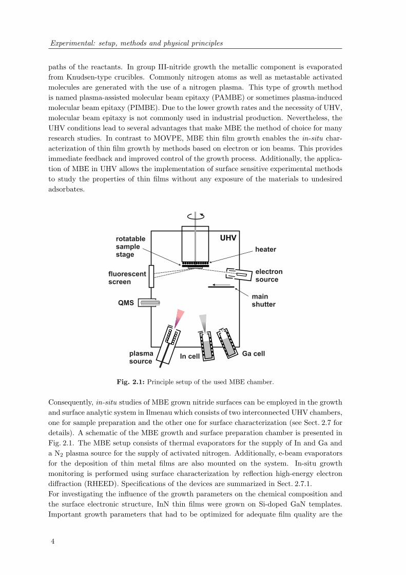
paths of the reactants. In group III-nitride growth the metallic component is evaporatedfrom Knudsen-type crucibles. Commonly nitrogen atoms as well as metastable activatedmolecules are generated with the use of a nitrogen plasma. This type of growth methodis named plasma-assisted molecular beam epitaxy (PAMBE) or sometimes plasma-inducedmolecular beam epitaxy (PIMBE). Due to the lower growth rates and the necessity of UHV,molecular beam epitaxy is not commonly used in industrial production. Nevertheless, theUHV conditions lead to several advantages that make MBE the method of choice for manyresearch studies. In contrast to MOVPE, MBE thin film growth enables the in-situ char-acterization of thin film growth by methods based on electron or ion beams. This providesimmediate feedback and improved control of the growth process. Additionally, the applica-tion of MBE in UHV allows the implementation of surface sensitive experimental methodsto study the properties of thin films without any exposure of the materials to undesiredadsorbates.
UHVrotatablesamplestage
heater
electron source
main shutter
fluorescentscreen
In cell Ga cellplasmasource
QMS
Fig. 2.1: Principle setup of the used MBE chamber.
Consequently, in-situ studies of MBE grown nitride surfaces can be employed in the growthand surface analytic system in Ilmenau which consists of two interconnected UHV chambers,one for sample preparation and the other one for surface characterization (see Sect. 2.7 fordetails). A schematic of the MBE growth and surface preparation chamber is presented inFig. 2.1. The MBE setup consists of thermal evaporators for the supply of In and Ga anda N2 plasma source for the supply of activated nitrogen. Additionally, e-beam evaporatorsfor the deposition of thin metal films are also mounted on the system. In-situ growthmonitoring is performed using surface characterization by reflection high-energy electrondiffraction (RHEED). Specifications of the devices are summarized in Sect. 2.7.1.For investigating the influence of the growth parameters on the chemical composition andthe surface electronic structure, InN thin films were grown on Si-doped GaN templates.Important growth parameters that had to be optimized for adequate film quality are the
2.2 Reflection high-energy electron diffraction (RHEED)
substrate temperature during growth as well as the flux of impinging indium atoms atthe surface, defined by the temperature of the Knudsen cell [1]. Since the small MBEchamber is equipped with a turbo molecular pump that has a relatively low pumping speed(300 l/s), the growth rate is mainly restricted by the flow of reactive nitrogen, since theplasma discharge breaks down at too high nitrogen pressures. Therefore, the N2 partialpressure was kept constant at high, but stable pressure conditions and was not regarded asan adjustable parameter for MBE growth.
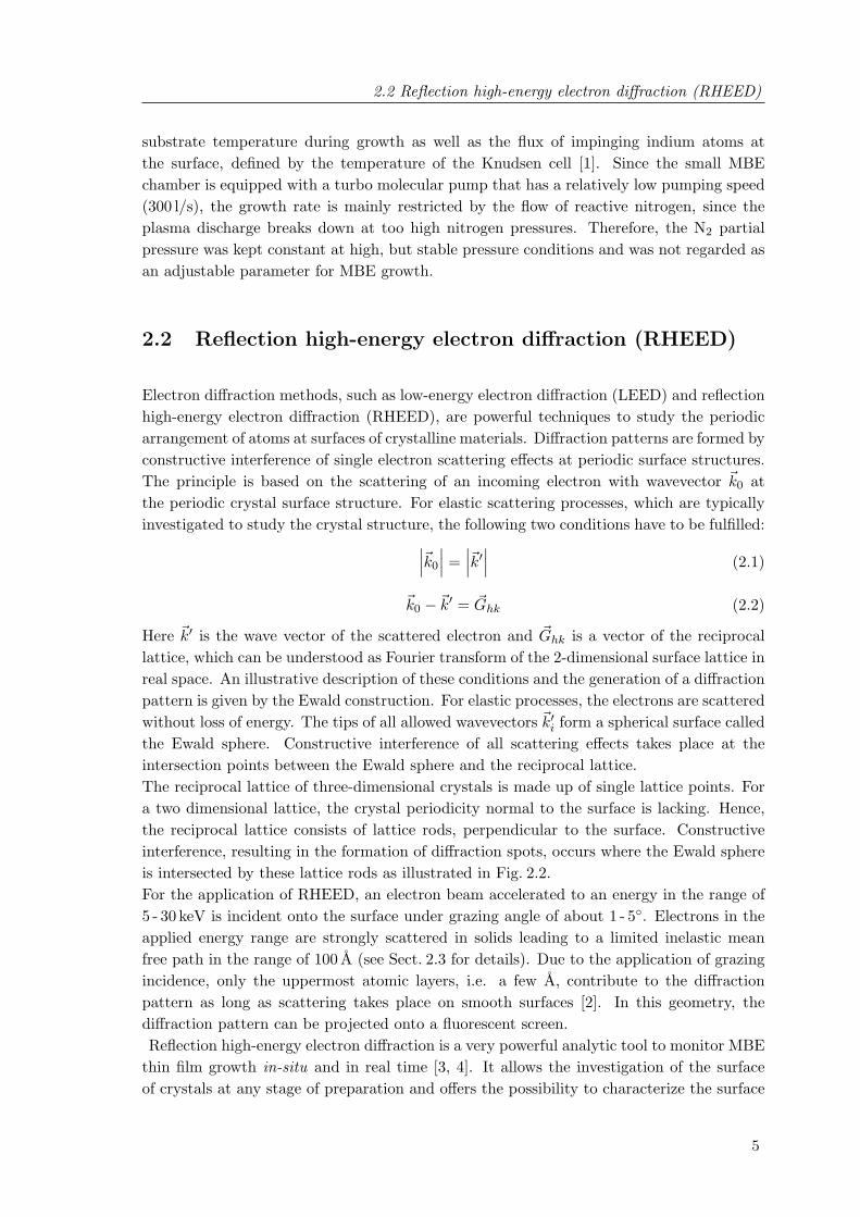
2.2 Reflection high-energy electron diffraction (RHEED)
Electron diffraction methods, such as low-energy electron diffraction (LEED) and reflectionhigh-energy electron diffraction (RHEED), are powerful techniques to study the periodicarrangement of atoms at surfaces of crystalline materials. Diffraction patterns are formed byconstructive interference of single electron scattering effects at periodic surface structures.The principle is based on the scattering of an incoming electron with wavevector ~k0 atthe periodic crystal surface structure. For elastic scattering processes, which are typicallyinvestigated to study the crystal structure, the following two conditions have to be fulfilled:∣∣∣~k0
∣∣∣ = ∣∣∣~k′∣∣∣ (2.1)
~k0 − ~k′ = ~Ghk (2.2)
Here ~k′ is the wave vector of the scattered electron and ~Ghk is a vector of the reciprocallattice, which can be understood as Fourier transform of the 2-dimensional surface lattice inreal space. An illustrative description of these conditions and the generation of a diffractionpattern is given by the Ewald construction. For elastic processes, the electrons are scatteredwithout loss of energy. The tips of all allowed wavevectors ~k′i form a spherical surface calledthe Ewald sphere. Constructive interference of all scattering effects takes place at theintersection points between the Ewald sphere and the reciprocal lattice.The reciprocal lattice of three-dimensional crystals is made up of single lattice points. Fora two dimensional lattice, the crystal periodicity normal to the surface is lacking. Hence,the reciprocal lattice consists of lattice rods, perpendicular to the surface. Constructiveinterference, resulting in the formation of diffraction spots, occurs where the Ewald sphereis intersected by these lattice rods as illustrated in Fig. 2.2.For the application of RHEED, an electron beam accelerated to an energy in the range of5 - 30 keV is incident onto the surface under grazing angle of about 1 - 5. Electrons in theapplied energy range are strongly scattered in solids leading to a limited inelastic meanfree path in the range of 100 A (see Sect. 2.3 for details). Due to the application of grazingincidence, only the uppermost atomic layers, i.e. a few A, contribute to the diffractionpattern as long as scattering takes place on smooth surfaces [2]. In this geometry, thediffraction pattern can be projected onto a fluorescent screen.Reflection high-energy electron diffraction is a very powerful analytic tool to monitor MBE
thin film growth in-situ and in real time [3, 4]. It allows the investigation of the surfaceof crystals at any stage of preparation and offers the possibility to characterize the surface

Experimental: setup, methods and physical principles
k0
k ’I
k ’II
-e
sample
Ewald sphere
sc
ree
n
reciprocal lattice
sampleside view
top view-e
Fig. 2.2: Schematic of the Ewald construction and generation of the RHEED pattern.
qualitatively with respect to crystallinity, morphology, surface reconstructions and latticeparameters. On real surfaces, terraces and atomic steps occur which limit the long-rangeorder of the surface. This non-ideality leads to broadening of the reciprocal rods whosewidth ∆S is proportional to the inverse length L of the ordered region over which thereis coherent scattering. The broadened rods form streaks in the RHEED pattern as theyintersect the Ewald sphere. To a first approximation, the width w of the streaks on theRHEED screen is proportional to the width of the rods in reciprocal space as long as thedivergence of the incident electron beam can be neglected [3]:
w ∝ ∆S =2π
L(2.3)
If the domain size, i.e. the typical distance between surface steps or other imperfections, issmaller than the natural coherence length of the electron beam (about 1000 A), the RHEEDpattern will be significantly broadened. Therefore, analyzing the width of the streaks pro-vides information about the surface order.As already indicated above, RHEED is not strictly limited to the uppermost atomic layers.Rough surfaces can exhibit islands which are small enough to be penetrated by the scatteredelectrons. In this case, diffraction represents the whole three-dimensional periodicity of thecrystal, leading to the formation of transmission spots within the streaks in the diffractionpattern [3]. This can be used as an indicator for 3-dimensional growth (island formation)during MBE.For the evaluation of the lattice constant, the distance d of the streaks on the RHEEDscreen has to be monitored. To a first approximation, it is proportional to the spacingof the rods in the two-dimensional reciprocal space, i.e. the length of the basic reciprocalin-plane lattice vectors ~Ghk. As a consequence, changes in the lattice constants during filmgrowth can be measured and the relaxation of incorporated strain during heteroepitaxy due
2.3 Photoelectron spectroscopy (PES)
a1
a2
a3
[]
1010
[ ]1100
[]
2110
[]
1210
[]
0110
[]
1010 []
11
20
[]
2110
[]
11
20
[] 1100
[]
0110
[]
1210
[0001]
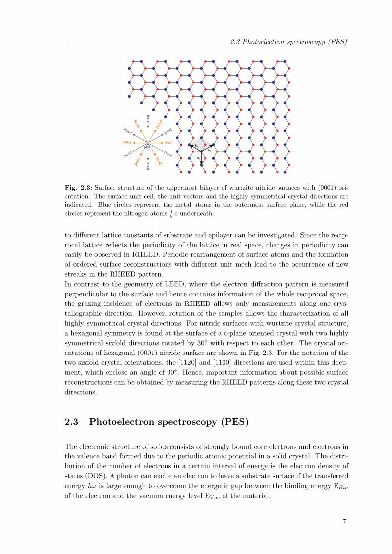
Fig. 2.3: Surface structure of the uppermost bilayer of wurtzite nitride surfaces with (0001) ori-entation. The surface unit cell, the unit vectors and the highly symmetrical crystal directions areindicated. Blue circles represent the metal atoms in the outermost surface plane, while the redcircles represent the nitrogen atoms 1
8 c underneath.
to different lattice constants of substrate and epilayer can be investigated. Since the recip-rocal lattice reflects the periodicity of the lattice in real space, changes in periodicity caneasily be observed in RHEED. Periodic rearrangement of surface atoms and the formationof ordered surface reconstructions with different unit mesh lead to the occurrence of newstreaks in the RHEED pattern.In contrast to the geometry of LEED, where the electron diffraction pattern is measuredperpendicular to the surface and hence contains information of the whole reciprocal space,the grazing incidence of electrons in RHEED allows only measurements along one crys-tallographic direction. However, rotation of the samples allows the characterization of allhighly symmetrical crystal directions. For nitride surfaces with wurtzite crystal structure,a hexagonal symmetry is found at the surface of a c-plane oriented crystal with two highlysymmetrical sixfold directions rotated by 30 with respect to each other. The crystal ori-entations of hexagonal (0001) nitride surface are shown in Fig. 2.3. For the notation of thetwo sixfold crystal orientations, the [1120] and [1100] directions are used within this docu-ment, which enclose an angle of 90. Hence, important information about possible surfacereconstructions can be obtained by measuring the RHEED patterns along these two crystaldirections.
2.3 Photoelectron spectroscopy (PES)
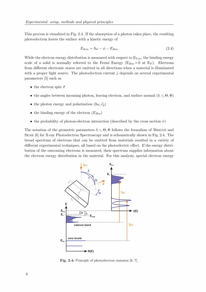
The electronic structure of solids consists of strongly bound core electrons and electrons inthe valence band formed due to the periodic atomic potential in a solid crystal. The distri-bution of the number of electrons in a certain interval of energy is the electron density ofstates (DOS). A photon can excite an electron to leave a substrate surface if the transferredenergy ~ω is large enough to overcome the energetic gap between the binding energy EBin
of the electron and the vacuum energy level EV ac of the material.
Experimental: setup, methods and physical principles
This process is visualized in Fig. 2.4. If the absorption of a photon takes place, the resultingphotoelectron leaves the surface with a kinetic energy of
EKin = ~ω − φ− EBin (2.4)
While the electron energy distribution is measured with respect to EV ac, the binding energyscale of a solid is normally referred to the Fermi Energy (EBin = 0 at EF ). Electronsfrom different electronic states are emitted in all directions when a material is illuminatedwith a proper light source. The photoelectron current j depends on several experimentalparameters [5] such as
• the electron spin ~σ
• the angles between incoming photon, leaving electron, and surface normal (δ, γ, Θ,Φ)
• the photon energy and polarization (~ω,~ep)
• the binding energy of the electron (EBin)
• the probability of photon-electron interaction (described by the cross section σ)
The notation of the geometric parameters δ, γ,Θ,Φ follows the formalism of Briggs andSeah [6] for X-ray Photoelectron Spectroscopy and is schematically shown in Fig. 2.4. Thebroad spectrum of electrons that can be emitted from materials resulted in a variety ofdifferent experimental techniques, all based on the photoelectric effect. If the energy distri-bution of the outcoming electrons is measured, their spectrum supplies information aboutthe electron energy distribution in the material. For this analysis, special electron energy
EKin
I(E)
EF
EF
EVac
valence band
core levels
N(E)
E
φ
EBin
yz
x -e
γ
δ
Θ
Φ
IP
EVBM
Fig. 2.4: Principle of photoelectron emission [6, 7].
2.3 Photoelectron spectroscopy (PES)
analyzers are used which are based on the deflection of electrons in an electric field. Amongthe variety of different setups, the most common used are the Cylindrical Mirror Ana-lyzer (CMA) and the Concentric Hemispherical Analyzer (CHA) or also named SphericalDeflection Analyzer (SDA). In this work photoelectron spectra have been measured withanalyzers of the hemispherical type. The principle and parts of the electron energy analyzer(EA 125) are described in Sect. 2.5.4.
2.3.1 Theory of photoelectron emission
From an atomic view, photoelectron spectra can be described by an isotropic three-stepmodel [5, 7]. The processes involved in the emission of a photoelectron are typically con-sidered separately in the following sequence:
1. local absorption of a photon combined with excitation of an electron
2. transport of the electron to the surface with the possibility of inelastic scattering
3. escape of the electron through the surface
The measured spectrum consists of a superposition of primary electrons Ip(E, ~ω) whichhave not suffered an inelastic collision and a background of secondary electrons Is(E, ~ω)which have lost energy during one or more scattering events.
I(E, ~ω) = Ip(E, ~ω) + Is(E, ~ω) (2.5)
According to the three-step model the primary electron distribution is described by
Ip(E, ~ω) = P (E, ~ω)× T (E)×D(E) (2.6)
Proposed models for the transmission function T (E) and the escape function D(E) havebeen reviewed in [5].
To derive the photoelectron generation rate, which is represented by the function P (E, ~ω),one has to consider all possible combinations that an electron is excited by a photon from itsinitial occupied state |i〉 into a final unoccupied electron state |f〉. Assuming that the crys-tal momentum ~k is conserved, the absorption process can be described by Fermi’s GoldenRule:
P (E, ~ω) ∝∑i,f
∫|Mi,f |2 · δ
(Ef (~k)− Ei(~k)− ~ω
)× δ(Ef (~k)− E
)d3k (2.7)
Here Mi,f = 〈f | ~A · ~p + ~p · ~A|i〉 is the dipole matrix element, ~A is the electromagneticvector potential and ~p is the momentum operator of the emitted electron. On the basisof this formula a comparison of the photoelectron spectra with theoretical band structurecalculations is possible. For the practical application in an experiment the number ofemitted primary electrons can be described in approximation by [8]
Ip(~ee, Ef , ~ω) ∝∫|Mi,f |2 ·Di(Ei)Df (Ei + ~ω) dEi (2.8)
Experimental: setup, methods and physical principles
The vector ~ee defines the direction of the detected electrons and Di and Df are the localdensity of states (DOS) of the initial and final states. Normally PES measurements are im-plemented using sources that emit light with a constant photon energy (UV or X-ray) andthe emitted photoelectrons are analyzed by the measurement of an “Energy DistributionCurve” (EDC). Measured EDC’s are always a convolution of the DOS of the initial andfinal states which can be described in terms of a “Joint Density of States” (JDOS).
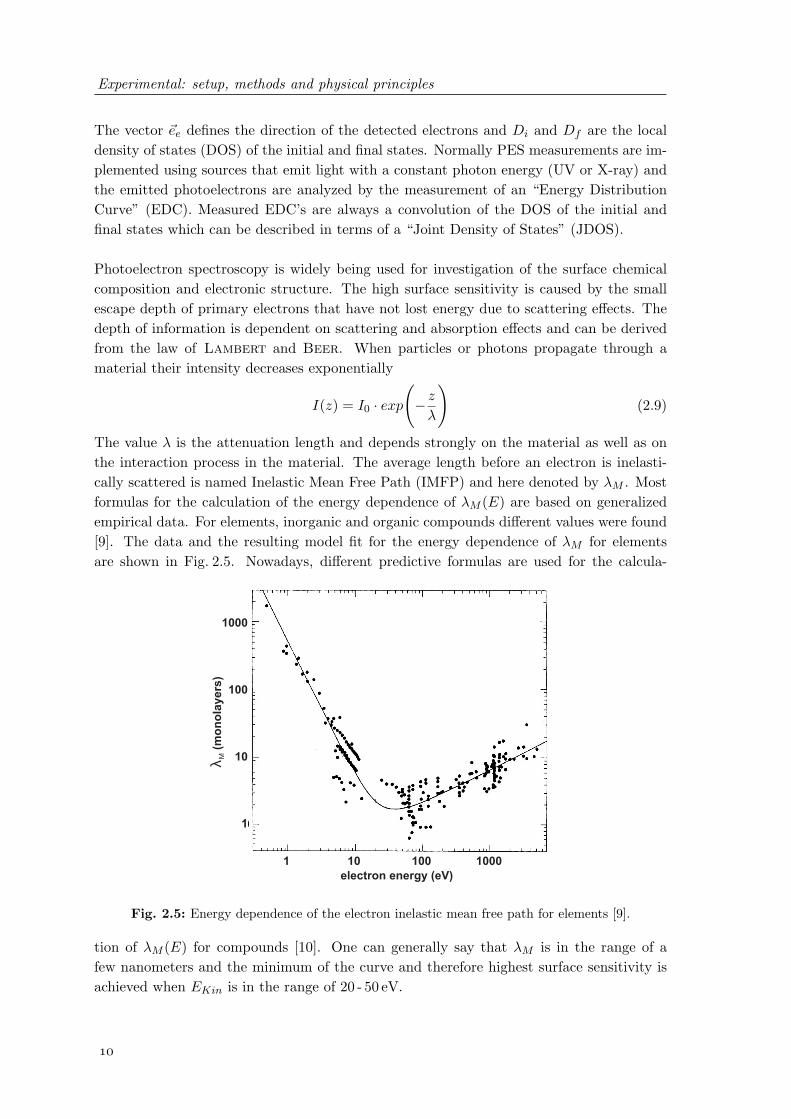
Photoelectron spectroscopy is widely being used for investigation of the surface chemicalcomposition and electronic structure. The high surface sensitivity is caused by the smallescape depth of primary electrons that have not lost energy due to scattering effects. Thedepth of information is dependent on scattering and absorption effects and can be derivedfrom the law of Lambert and Beer. When particles or photons propagate through amaterial their intensity decreases exponentially
I(z) = I0 · exp
(− z
λ
)(2.9)
The value λ is the attenuation length and depends strongly on the material as well as onthe interaction process in the material. The average length before an electron is inelasti-cally scattered is named Inelastic Mean Free Path (IMFP) and here denoted by λM . Mostformulas for the calculation of the energy dependence of λM (E) are based on generalizedempirical data. For elements, inorganic and organic compounds different values were found[9]. The data and the resulting model fit for the energy dependence of λM for elementsare shown in Fig. 2.5. Nowadays, different predictive formulas are used for the calcula-
electron energy (eV)
λ (
mo
no
lay
ers
)M
1000
100
10
1
1 10 100 1000
Fig. 2.5: Energy dependence of the electron inelastic mean free path for elements [9].
tion of λM (E) for compounds [10]. One can generally say that λM is in the range of afew nanometers and the minimum of the curve and therefore highest surface sensitivity isachieved when EKin is in the range of 20 - 50 eV.
2.3 Photoelectron spectroscopy (PES)
2.3.2 X-ray photoelectron spectroscopy (XPS)
Two main PES methods have been developed with the aim to determine the electronicstructure of materials. This is historically related to the available laboratory excitationsources. For X-ray photoelectron spectroscopy (XPS), MgKα or AlKα radiation is normallyused. With XPS, the chemical composition of a surface can be determined by measuringthe emission from core levels. By a careful analysis of the core level binding energy andthe emission intensity, information on the chemical environment of the atoms as well asthe stoichiometry of the material can be obtained. Therefore, it is also named ElectronSpectroscopy for Chemical Analysis (ESCA).Quantitative analysis is normally based on the comparison of the measured peak area totheoretical predictions of the photoelectron signal. Under the assumption that the reflectionof X-rays on the investigated surface or interface is negligible and the X-ray intensity in theinvestigated material is constant (this is normally the case because the attenuation lengthof X-rays in matter is much greater than the information depth of PES), the XPS core levelintensity of an element i can be described by [6]
Ii(Θ) = J0 sec(δ)σi(~ω)Li(γ, ~ω)T (Ei)D(Ei) ·∫
Ni(z)× exp
(− z
λm(Ei) cos(Θ)
)dz
(2.10)where J0 is the flux of X-rays per unit area onto the sample, σi(~ω) is the radiation de-pendent cross-section which describes the probability for the generation of a photoelectron.T (Ei) is the analyzer transmission function and D(Ei) the detection efficiency for electronsof a certain kinetic energy. The last value is normally assumed to be constant for themeasured values of EKin. Furthermore Li(γ, ~ω) describes the angular dependence of thephotoemission from a single atom and relies on the angle between the incoming photonsand the emitted electrons as well as the used photon energy [11]. The density of the atomspecies i is assumed to be only varying in the direction perpendicular to the surface planeand λM (Ei) is the previously described inelastic mean free path of an electron with thekinetic energy Ei. From this formula models can be derived, for example to determine thestoichiometry of the material or to calculate the thickness d of a thin and uniform overlayer.With the aid of a monochromated X-ray source or synchrotron radiation, it is furthermorepossible to analyze the valence band structure of materials.
2.3.3 Ultra-violet photoelectron spectroscopy (UPS)
Ultra-violet photoelectron spectroscopy is employed using photon energies below 100 eVwhich are not suitable for probing deep core levels. However, the photoelectric cross-sectionsfor valence band electrons are very high in this energy range. Consequently, occupied statesof the valence band of semiconductors and insulators as well as of the conduction band ofmetals can be investigated to analyze, for example, the energy of the valence band maximumwith respect to the Fermi level. Under the assumption of a known band gap, the electronaffinity χ of a material as well as the conduction band offset of thin films can also bedetermined.The interpretation of structures in UPS is far more complicated than in XPS. All elements

Experimental: setup, methods and physical principles
exhibit various states in the valence band which are not separated from each other as it is thecase for the core states. Furthermore, these states participate strongly in chemical bonding,building up energy bands which result in rather broad features. As a result, support bytheoretical calculations of chemical bonds and their respective density of states is in mostcases required. For UPS, the photon energy is in a range where resonant transitions intofinal electron states according to the dipole matrix element Mi,f = 〈i| ~A · ~p + ~p · ~A|f〉 canplay an important role in the photoemission process and have to be considered as well.The break of periodicity at the surfaces leads to energy states different from those in thebulk. These surface states are localized at the surface and decay exponentially both intothe bulk and vacuum. As can be seen in Fig. 2.5, the inelastic mean free path for kineticenergies around 50 eV is in the range of single atomic layers leading to a very high surfacesensitivity. Therefore, UPS allows the investigation of surfaces with respect to surface statesand adsorbates, such as atoms and small molecules. Surface states often reside in the bulkband gap resulting in band bending and Fermi level pinning at the surface [12] and are verysensitive to surface treatment which eases their identification using UPS.
2.3.4 Secondary electron emission (SEE)
For the investigation of occupied states in the valence band as well as chemical analysisusing core level photoemission, in many cases, electrons are analyzed that have not sufferedany loss of energy due to scattering during their transport to the surface. However anygenerated photoelectron can be subject of manifold interactions with other electrons orquasiparticles inside the material leading to characteristic losses of energy. An importantexample is the excitation of plasmons, which results in characteristic structures in XPSspectra at higher binding energies close to the parent line. [7, 5]Besides these characteristic single scattering effects, many electrons are subject of multipleinteractions resulting in a broad and featureless electron background and an intense cascadepeak at the low energy end of the photoemission spectrum. Hence, the measured photoe-mission spectrum is a superposition of the signal coming from the primary photoelectronsand the contribution of all secondary electrons (see Eq. 2.5). The majority of these socalled secondary electrons are most commonly accepted to be produced via direct trans-fer of energy from the primary photoelectron to electrons in bound states or filled valenceband states, thereby promoting them to empty conduction states (interband transitions).Other important mechanisms are excitation of phonons, electron-hole pair creation as wellas decay processes of excited electrons. This also involves a cascade process in which higherenergy secondary electrons produce more secondaries thereby degrading in energy as theymigrate to the surface [13]. From the low energy cut-off of this cascade structure one candetermine the work function of the material, after having performed calibration measure-ments on reference samples (e.g. Au or Ag). For that purpose, in some cases it is necessaryto apply a negative voltage of a few volts to the sample in order to overcome the workfunction of the electron analyzer and to avoid disturbing signals from tertiary electronswhich are generated by interaction of electrons with the analyzer material.As already mentioned, the secondary electrons roll down through the states in the con-duction band due to inelastic scattering and pile up at the high density of conduction
2.4 Electron energy loss spectroscopy (EELS)
states. These electrons can also be emitted into the vacuum leading to structures insidethe otherwise featureless distribution of the cascade peak. This aspect has been used forstudies of empty states of metals as well as oxide surfaces using electron-induced angle-resolved secondary-electron spectroscopy (ARSES) [14, 13]. For photon-induced electronspectroscopy measurements, the processes of secondary electron generation are qualita-tively the same, enabling the study of unoccupied states above the vacuum level EV ac
using angle-resolved ultra-violet photoemission measurements [15].
2.4 Electron energy loss spectroscopy (EELS)
The measurement of the energy distribution of electrons that have been scattered from orthrough a material is named electron energy loss spectroscopy (EELS). For the study ofsurface properties, an electron beam with a primary energy E0 and a narrow energetic band-width ∆E0 is focused onto a sample and the reflected electrons are analyzed with respect totheir spectral distribution. For impinging electrons the same is valid as for photoelectrons,they can be involved in scattering processes resulting in characteristic energy losses. Forconventional EELS experiments, electrons with E0 ranging from 100 eV to a few keV canpartly penetrate into the solid. The scattering cross section in this case is proportional tothe bulk loss function [16]
=(
1ε(ω)
)(2.11)
and is therefore directly linked to the dielectric properties ε(ω) of a material. For con-ventional EELS, the standard equipment for Auger and photoelectron spectroscopy can beused, such as hemispherical electron analyzer and a standard electron source. With thismethod, excitation of electrons from occupied states in the valence band to empty states(interband transitions) can be investigated, which give insight into the band structure of amaterial. Furthermore, the energy of collective excitations of valence electrons (bulk andsurface plasmons) can be determined.Low energy losses of 10−3 to 1 eV correspond to the excitation of phonons and vibrationalmodes of adsorbate molecules and are usually subject of high resolution electron energy lossspectroscopy (HREELS) using slow electrons. In the case of a specular geometry, dipolescattering at the surface has to be regarded, resulting in a cross section proportional to thesurface loss function [16]
=(
1ε(ω) + 1
)(2.12)
In addition to the vibrational structure of surfaces, carrier plasmon excitations of semicon-ductors that have an energy depending on the carrier concentration n, the effective electronmass m∗ and the high frequency dielectric constant ε∞ of a material
ω2p =
(ne2
ε∞ε0m∗
)(2.13)
can be studied. By implementation of measurements with varying primary electron energyin combination with sophisticated modeling of the loss function, by solving the Schrodinger-

Experimental: setup, methods and physical principles
Poission equation self-consistently, it is possible to derive the carrier density and band profileat semiconductor surfaces and interfaces [17, 18].
2.5 Excitation sources and electron detection
2.5.1 X-ray source for XPS
All presented core level measurements have been performed using a special X-ray sourcethat is combined with a monochromator (XM1000). This system consists of an AlKα X-raytube with a small spot filament and a quartz Bragg crystal installed in a geometry of a 500mm diameter Rowland circle. X-rays from the source are reflected by the quartz crystalBragg mirror and focused onto the sample in a 1:1 projection. The principle componentsof the monochromator setup are shown in Fig. 2.6. The removal of the Kα2 line by the
Bragg crystal
sample
X-ray source
electron analyzer
Rowland circle
Fig. 2.6: Principle components of the monochromated X-ray source [19].
Bragg monochromator is one important advantage of this type of X-ray source, resultingin a slightly shifted photon energy (~ω =1486.7 eV). As a consequence, the line width ofthe generated photon is strongly reduced (FWHM =0.25 eV) compared to standard X-ray sources (FWHM =0.7 eV for MgKα and 0.85 eV for AlKα). This effect results in animproved energy resolution, which is important for the detection of small shifts in the corelevel binding energy. Another benefit from the use of a monochromator is the absence ofany disturbing satellite lines (e.g. Kα3,4). Furthermore, the sample is exposed to less heatradiation and the Bremsstrahlung background is removed, which improves the signal tonoise ratio. Additionally, due to the special geometry, fast electrons that are generatedinside the X-ray tube have no influence on the spectra. Altogether, these improvementsare important and allow the measurement of the valence electrons using X-ray radiation.In that way, the bulk-like valence band density of states can be precisely measured.Due to the use of a small spot filament, the irradiated sample area is reduced to a size ofless than 1mm in diameter which allows the selective analysis of small samples excludingthe appearance of photoelectrons from the surrounding material. The source is typicallyoperated at UHV =14 kV and IE =21 mA.

2.5 Excitation sources and electron detection
2.5.2 HIS13 VUV light source for UPS
The UPS UV light source (HIS13) is a water cooled high intensity discharge lamp (seeFig. 2.7) that is directly adapted to the UHV system and allows the windowless illumi-nation of the sample surface. The gas inlet is controlled by a double differential pumpingsystem consisting of a rotary pump on the first stage and a combination of rotary and turbomolecular pump on the second pumping stage. This setup provides the possibility of accu-rate setting of the gas pressure inside the discharge capillary and restricts the undesirablepressure rise in the UHV chamber. Among the several discharge gases that can be used forgeneration of UV light (Ar, H2, He, Kr, Ne, Xe), helium is used in this work to investigatethe valence band structure of InN, In2O3 and ITO. The operation principle of the HIS13
water cooling
cathode anode
discharge capillary
lightcapillary
Fig. 2.7: Functional parts of the HIS13 VUV lamp [20].
is based on a cold cathode capillary discharge that can be influenced by adjusting the gaspartial pressure as well as the current flow of the discharge. Normally, two modes of lightemission are possible:
1. Light emission from neutral atoms - He I radiation (~ω =21.22 eV)In this case, the VUV light is generated in the positive column of the discharge. Theoperation mode is normally achieved at higher partial pressures.
2. Light emission from singly charged ions - He II radiation (~ω = 40.81 eV)This radiation type is essentially produced from the cathode fall which is normallylocated very close to the cathode surface. To achieve this behavior, the dischargemust be operated at a very low pressure together with higher discharge currents.
The discharge lamp is operated using a 300mA power supply with a stability of < 10-4.This provides intensity fluctuations of less than 1% if the gas pressure is stabilized. It hasto be pointed out that the HIS13 operation parameters can be set to achieve almost pureHe I generation which results in the absence of disturbing contributions from He II in themeasured spectrum (pressure of pHe∼ 4×10⁻² mbar at first pumping stage and I= 100 mA).However, if the lamp is operated in the second mode, the generation of He I radiation canonly by reduced to a certain limit. For the given setup, the achievable intensity ratioIHe II / IHe I is ∼ 10% at pHe =5×10⁻³ mbar and I= 300 mA.Besides the main lines at 21.22 eV and 40.81 eV, satellite lines are also generated in the gasdischarge and have to be taken into consideration for the interpretation of UPS spectra.

Experimental: setup, methods and physical principles
For the helium discharge, details of the energies and intensities of the different generatedphotons are given in Tab. 2.1.
VUV source ~ω (eV) rel. intensity (%) λ (nm) satellite shift (eV)
He I α 21.22 100.0 58.43 -β 23.09 1.2...1.8 53.70 1.87γ 23.74 0.5 52.22 2.52
He II α 40.81 100.0 30.38 -β 48.37 <10.0 25.63 7.56γ 51.02 n.a. 24.30 10.20
Tab. 2.1: Photon energy and intensity of the spectral lines generated in the VUV discharge lampHIS13 when operated with helium [20]. The FWHM of the He I and He II main spectral lines isbelow 10 meV.
For the investigation of the valence electrons in indium compounds, the emission from theshallow In4d semi-core level excited using He II radiation is a very sensitive indicator forchanges at the surface. On the other hand, however, this signal interferes with the emissionof electrons close to the Fermi edge excited by He I radiation. Additionally, the generatedsatellite lines of the In4d level disturb the analysis of the valence band distribution of He IIspectra. These two factors have to be kept in mind for the analysis of the measurementsin the following chapters.
2.5.3 EKF 1000 electron source for EELS
The EKF 1000 is an electron source for the application in AES and EELS experiments.The functional parts of this device are shown in Fig. 2.8. Electrons are generated by aheated LaB6 filament and are accelerated to an energy of 100 eV to 5 keV by a Wehneltgrid assembly, pass through an electrostatic lens system (condenser lens, aperture and focuslens) that allows to vary the current flow and to set the focal distance of the source in orderto adjust the beam diameter at the sample (minimum diameter < 2 µm). A deflectionsystem, consisting of quadrupole x/y-deflectors are employed for static and dynamic beamdeflection, and can be used in combination with a scanning unit for SAM and SEM imaging.The emission-regulated LaB6 filament provides reliably and stable emission conditions and
sample
focuscondenser
aperture x,y-deflection
LaB 6
cathode
Fig. 2.8: Functional parts of the EKF 1000 electron source.
2.5 Excitation sources and electron detection
a high beam current necessary for quantitative analysis of electron spectra (the source isnormally operated at an emission current of 40 µA).
2.5.4 Hemispherical electron analyzer
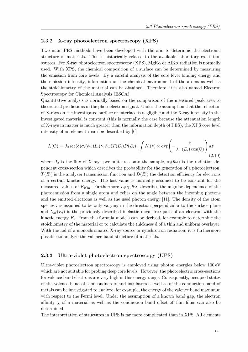
To analyze the distribution I(E) of emitted electrons, a concentric hemispherical analyzer(CHA) is used. A schematic of the setup is shown in Fig. 2.9. It consists of an electrostaticlens system, a hemispherical deflection unit and an electron detection unit. The electrons
R1
R0R2
channeltron
outer sphere - V2
inner sphere - V1
retardation
angularacceptance
sample
αentrance slit d1
exit slit d2
Fig. 2.9: Principle setup of a concentric hemispherical electron analyzer.
emitted from the sample are collected by the lens system and focused onto the entranceaperture of the analyzer. The setting of the first lens defines the analysed area and angularacceptance from where electrons are collected. The second lens retards or accelerates theelectrons to match the pass energy of the analyzer. The analyzer itself consists of twohemispherical electrodes with the radii R1 and R2 and an applied voltage of V1 and V2,respectively. Electrons with an energy Ep that pass the lens system and enter the analyzertangentially to the median surface at R0, can only pass the analyzer in a circular orbit, ifthe electron energy matches the following condition
Ep =e · (V2 − V1)
R2R1
− R1R2
(2.14)
Due to the finite size d of the analyzer entrance and exit apertures, electrons with a differentenergy as Ep can pass the analyzer if they have a slightly different entrance angle. Con-sequently, a bundle of different electron trajectories for electrons with an energy Ep ±∆E
are possible. This defines the resulting analyzer energy resolution
∆E = Ep · (d
2R0+ α2) (2.15)
Experimental: setup, methods and physical principles
The parameter α is called angular acceptance of the analyzer and depends on the settingsof the electrostatic lens system in front of the sample surface. The electrons that passthe analyzer and leave through the exit aperture are amplified by an electron multiplier(channeltron). The measured current is proportional to the number of electrons if the signalintensity is not such high that saturation effects occur. The used EA125 is a multi-channelanalyzer system with 7 channel electron multipliers, placed across the exit plane of theanalyzer to improve statistics. The dispersion offset according to this setup is proportionalto the used pass energy and is normally calibrated with a reference sample.The analyzer can be operated in constant pass energy mode (CPE or CAE) with Ep = const.
or in constant retardation mode (CRR) where Ep/E = const. The chosen mode defines theanalyzer transfer function which is ideally T (E) ∝ 1/E for CAE and T (E) ∝ E for CRR,respectively.
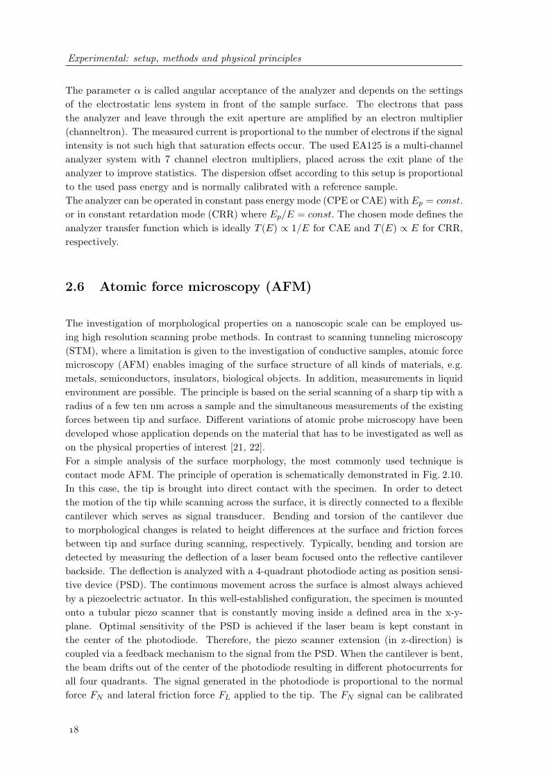
2.6 Atomic force microscopy (AFM)
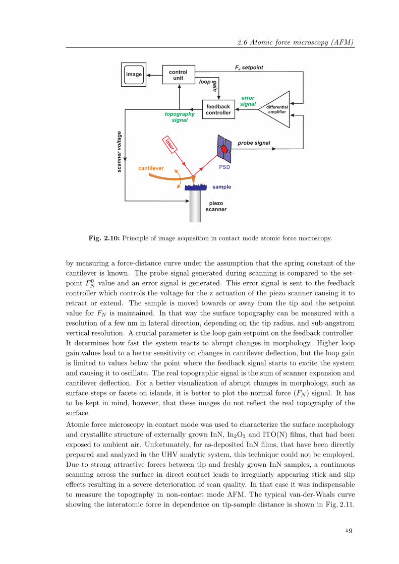
The investigation of morphological properties on a nanoscopic scale can be employed us-ing high resolution scanning probe methods. In contrast to scanning tunneling microscopy(STM), where a limitation is given to the investigation of conductive samples, atomic forcemicroscopy (AFM) enables imaging of the surface structure of all kinds of materials, e.g.metals, semiconductors, insulators, biological objects. In addition, measurements in liquidenvironment are possible. The principle is based on the serial scanning of a sharp tip with aradius of a few ten nm across a sample and the simultaneous measurements of the existingforces between tip and surface. Different variations of atomic probe microscopy have beendeveloped whose application depends on the material that has to be investigated as well ason the physical properties of interest [21, 22].For a simple analysis of the surface morphology, the most commonly used technique iscontact mode AFM. The principle of operation is schematically demonstrated in Fig. 2.10.In this case, the tip is brought into direct contact with the specimen. In order to detectthe motion of the tip while scanning across the surface, it is directly connected to a flexiblecantilever which serves as signal transducer. Bending and torsion of the cantilever dueto morphological changes is related to height differences at the surface and friction forcesbetween tip and surface during scanning, respectively. Typically, bending and torsion aredetected by measuring the deflection of a laser beam focused onto the reflective cantileverbackside. The deflection is analyzed with a 4-quadrant photodiode acting as position sensi-tive device (PSD). The continuous movement across the surface is almost always achievedby a piezoelectric actuator. In this well-established configuration, the specimen is mountedonto a tubular piezo scanner that is constantly moving inside a defined area in the x-y-plane. Optimal sensitivity of the PSD is achieved if the laser beam is kept constant inthe center of the photodiode. Therefore, the piezo scanner extension (in z-direction) iscoupled via a feedback mechanism to the signal from the PSD. When the cantilever is bent,the beam drifts out of the center of the photodiode resulting in different photocurrents forall four quadrants. The signal generated in the photodiode is proportional to the normalforce FN and lateral friction force FL applied to the tip. The FN signal can be calibrated
2.6 Atomic force microscopy (AFM)
feedbackcontroller
differentialamplifier
piezoscanner
sc
an
ne
r v
olt
ag
e
image
loop
sample
cantilever PSD
probe signal
F setpointN
errorsignal
topographysignal
laser
controlunit g
ain
Fig. 2.10: Principle of image acquisition in contact mode atomic force microscopy.
by measuring a force-distance curve under the assumption that the spring constant of thecantilever is known. The probe signal generated during scanning is compared to the set-point F 0
N value and an error signal is generated. This error signal is sent to the feedbackcontroller which controls the voltage for the z actuation of the piezo scanner causing it toretract or extend. The sample is moved towards or away from the tip and the setpointvalue for FN is maintained. In that way the surface topography can be measured with aresolution of a few nm in lateral direction, depending on the tip radius, and sub-angstromvertical resolution. A crucial parameter is the loop gain setpoint on the feedback controller.It determines how fast the system reacts to abrupt changes in morphology. Higher loopgain values lead to a better sensitivity on changes in cantilever deflection, but the loop gainis limited to values below the point where the feedback signal starts to excite the systemand causing it to oscillate. The real topographic signal is the sum of scanner expansion andcantilever deflection. For a better visualization of abrupt changes in morphology, such assurface steps or facets on islands, it is better to plot the normal force (FN ) signal. It hasto be kept in mind, however, that these images do not reflect the real topography of thesurface.
Atomic force microscopy in contact mode was used to characterize the surface morphologyand crystallite structure of externally grown InN, In2O3 and ITO(N) films, that had beenexposed to ambient air. Unfortunately, for as-deposited InN films, that have been directlyprepared and analyzed in the UHV analytic system, this technique could not be employed.Due to strong attractive forces between tip and freshly grown InN samples, a continuousscanning across the surface in direct contact leads to irregularly appearing stick and slipeffects resulting in a severe deterioration of scan quality. In that case it was indispensableto measure the topography in non-contact mode AFM. The typical van-der-Waals curveshowing the interatomic force in dependence on tip-sample distance is shown in Fig. 2.11.

Experimental: setup, methods and physical principles
distance
forc
e
repulsive forces
attractive forcesnon-contact
mode region
contact mode region
tapping mode region
Fig. 2.11: Interatomic force vs. distance curve between tip and sample in atomic force microscopy.Contact mode uses repulsive forces, while in non-contact mode the cantilever oscillates in the at-tractive force region. (after Oura et al. [2])
At relatively large distances the tip is weakly attracted by the sample due to van-der-Waals forces. With decreasing distance the attraction increases until repulsion occurs.This corresponds to electrostatic forces as the electron clouds of the sample and tip atomsoverlap and repel each other. While in contact mode the repulsive forces lead to a bendingof the cantilever, non-contact AFM is established by setting a stiff cantilever into vibrationclose to its resonance frequency (typically 100 to 400 kHz) at an amplitude of a few tens ofangstroms while scanning above the surface at a distance of the order of tens to hundredsof angstroms. During scanning in x-y direction as the tip comes closer to the surface, theforce gradient, which is the derivative of the force versus distance, changes with tip-to-sample separation, resulting in slight deviations of the cantilever resonance frequency. Innon-contact AFM, the variation of the cantilever resonance frequency ∆f is used as probesignal which is again compared to a setpoint value ∆f0 by a feedback controller. This signalis used to move the piezo scanner up and down in the z-direction in order to keep the spacingbetween tip and sample constant and, in this manner, obtain information about the surfacetopography. The small force values in the non-contact regime and the greater stiffnessof the cantilevers used for non-contact AFM are factors that make the signal small, andtherefore difficult to measure. Nevertheless, the sensitivity of this detection scheme providessub-angstrom vertical resolution in the image, as with contact AFM.

2.7 Growth and surface analysis system
2.7 Growth and surface analysis system
The experiments described in this work were carried out in a multi-technique ultra highvacuum (UHV) system located in the Center for Micro- and Nanotechnologies at the Tech-nical University Ilmenau. The complete system is a custom-made apparatus from Omicron
NanoTechnology GmbH, Taunusstein. It consists of two interconnected UHV chambers:a) the surface analytic chamber and b) the preparation and MBE growth chamber, both withbase pressures below 2×10⁻¹⁰ mbar, and a small sample introduction (load lock) chamber.The vacuum conditions are realized by a combination of turbo molecular and rotary pumpsas well as by ion getter and a titanium sublimation pump (TSP) on each of the two mainchambers. Photographs of the UHV system are shown in Fig. 2.12.
Fig. 2.12: Photographs of the growth and surface analysis system (left: surface analysis chamber,right: preparation and MBE growth chamber).
2.7.1 MBE growth and surface preparation chamber
The preparation and MBE growth chamber is a system designed for surface preparation andthin film growth. For the deposition of various materials it is equipped with electron beamevaporators (EFM 3), e.g. used for the evaporation of gold and silver, and two effusion cells(WEZ 40) with pyrolytic boron nitride (PBN) crucibles and Ta filaments. These Knudsencells are filled with indium and gallium, respectively, for InN and GaN growth. The activenitrogen is supplied by a SVT Associates RF4.5 plasma source which can be operated up to500 W. The different stages of nitride thin film growth as well as surface reconstructions canbe monitored by reflection high-energy electron diffraction (RHEED) using an EK-20-RSelectron source from Staib Instruments. This electron gun produces an electron beamwith kinetic energies up to 20 keV. The electron beam has an adjustable grazing angle ofincidence (1 - 5) and can be focused onto the surface with a spot size of less than 100µm.The diffraction pattern is visualized with a phosphorus screen and digitalized using a CCDcamera (PCO pixelfly).The sample stage consists of a rotatable manipulator stage with the capability of radiativeheating of the sample backside up to temperatures of 1200C. The sample temperature can
Experimental: setup, methods and physical principles
be referenced by a thermocouple mounted on the manipulator sample stage after carefultemperature calibration with a pyrometer. A quadrupole mass spectrometer (QMS) withFaraday cup and electron multiplier provides the possibility of residual gas analysis (RGA)in the MBE chamber during sample preparation in a scan range from 1 to 200 atomic massunits.For surface cleaning and preparation the chamber is further equipped with a cold cathodesputter gun (ISE 5) for Ar+ ion bombardment. It is mounted at an angle of ∼ 45 withrespect to the surface normal and can be operated in an energy range from 250 eV to 5 keVallowing a wide range of sputtering conditions.In order to further reduce contamination effects due to desorption of species from thereactor walls during growth at higher temperatures, the chamber has a cryo-shield forliquid nitrogen cooling which was always operated during thin film growth in this work. Inthat way the base pressure of the growth chamber could be further reduced by one orderof magnitude.
2.7.2 Surface analysis chamber
The chamber is designed to combine the advantages of electron spectroscopy methods suchas X-ray photoelectron spectroscopy (XPS), ultra-violet photoelectron spectroscopy (UPS),Auger-electron spectroscopy (AES) and electron energy loss spectroscopy (EELS) with thepossibility of investigating the morphology and the structural characteristics of sample sur-faces by atomic force microscopy (AFM), scanning tunneling microscopy (STM), photoelec-tron emission microscopy (PEEM) and scanning electron microscopy (SEM). As a result,the chemical composition, electronic properties and morphology of surfaces can be probedwithout removing the sample from UHV. For sample transfer and angle-resolved electronspectroscopy measurements the analytic chamber is equipped with a precision manipula-tor that allows sample positioning in all three directions and rotations along the analyzerplane in order to vary the emission angle in electron spectroscopy. The sample stage on theanalytic chamber manipulator enables specimen annealing via radiative heating from thebackside (up to ∼ 700 K) or cooling down to ∼ 120 K via liquid nitrogen (LN2) cooling.The different electron spectroscopy techniques are facilitated by several excitation sourcesmounted on the system. For AES and EELS measurements, the surface can be irradiatedby electrons from an EKF 1000 electron gun which uses a LaB6 cathode and provideselectrons of variable energy between 100 eV and 5 keV. The electron beam can further befocused to a spot size down to < 2 µm and scanned across the sample surface in order toperform SEM by secondary electron detection. XPS measurements can be performed usingtwo different X-ray sources. The first is a twin anode X-ray tube (DAR 400) that allowsthe generation of either MgKα (~ω = 1253.6 eV) or AlKα (~ω = 1486.6 eV) radiation. Forobtaining a better energy resolution in the XPS measurements, monochromated X-rayscan be generated by a system consisting of a X-ray source (Phi 10-610E) combined with aquartz crystal monochromator (XM 1000). To investigate the valence electrons by means ofUPS, a UV light source (HIS 13) is also mounted onto the chamber. The energy distributionof the emitted electrons are detected by a hemispherical electron analyzer (EA125) with anelectron mean path radius of 125 mm. The slit size at the entrance and exit of the analyzer
2.7 Growth and surface analysis system
can be varied by external rotary feedthroughs. Electrons are detected by seven electronmultipliers (channeltrons) placed across the exit plane of the analyzer. In case of necessaryelectron spectroscopy measurements on insulating samples, possible charging effects can beadequately compensated using a charge neutralizer (CN 10).The scanning probe microscopy (SPM) unit is a combined UHV – AFM/STM system whichworks at room temperature. For high resolution measurements, vibration decoupling is pro-vided by the AFM/STM base plate being suspended by four soft springs. The resonancefrequency of the spring suspension is about 1Hz. Vibrations of the system are preventedby an arrangement of permanent magnets which float the whole SPM base plate. For AFMthe light beam produced by a special bakeable infrared LED (λ =820 nm) is reflected fromthe cantilever backside onto the 4-section position sensitive detector (PSD) via two mir-rors which are magnetically mounted to piezo-driven actuators for beam alignment. Thescanner unit itself consists of a tube piezo crystal with a maximum scan area of 5×5 µm
and a maximum extension of ∼ 1 µm. Measurements can be performed in contact andnon-contact AFM mode as well as in STM mode with the further capability of performingscanning tunneling spectroscopy (STS).In addition to these conventional surface analysis techniques, a Focus IS-PEEM with µ-ESCA electron energy analyzer is attached to the analytic chamber. It enables measure-ments of the spatial distribution of emitted photoelectrons that are excited either by amercury lamp (HBO 103W/2) or a deuterium lamp (Heraeus D200F) with a specifiedstep-edge resolution of 20 nm. This system further allows ultra-violet photoelectron mi-crospectroscopy measurements in the micrometer range using a second VUV HIS 13 lightsource directly connected to the PEEM. More details, information and properties of thePEEM setup can be found in a previous work [23].
2.7.3 Load lock chamber
The load lock is equipped with a turbo pump (Varian) in combination with a rotary pump(Pfeiffer) to achieve a minimum pressure of∼ 5×10⁻⁸ mbar. It facilitates the simultaneousloading of two samples. A removable transport box is mounted onto the load lock fortransportation of samples to other systems without exposing them to ambient conditions,e.g. for electrical characterization of oxygen sensitive films in a glove box. This transportsystem has also been successfully used to transfer freshly grown nitride samples to a highresolution electron energy loss spectroscopy (HREELS) system for further characterizationof the vibrational signatures and the electronic properties of the surfaces. It allows thetransfer of samples without exceeding of the pressure above 1×10⁻⁵ mbar for ∼ 1 hour.For the deposition of organic molecules such as pentacene or C60, the load lock chambercan be further equipped with a self-made crucible evaporator to avoid any contaminationrelated to evaporation of carbon-based species in the main MBE chamber. The load locksystem is additionally connected to the gas inlet system in order to perform clean adsorptionexperiments at higher pressures than possible in the UHV system. Reactive gases with up to1 bar pressure can be offered to realize higher doses. After exposure, the system can quicklypumped down and the sample can be transferred and analyzed without being exposed toair.

Experimental: setup, methods and physical principles
2.7.4 Experimental details and specifications of the electron spectroscopy
measurements
This section summarizes the used experimental settings and parameters for the performedelectron spectroscopy studies. Most important aspects are i) a correct energy calibrationof the system in order to exactly determine important material parameters, like electronbinding energy, distance between valence band maximum (VBM) and Fermi level as well asthe work function, and ii) determination of the energy resolution of the measurements. Thecalibration of the electron analyzer is regularly performed by measurement of the Ag3d5/2
core level emission and an exact determination of the position of the Fermi edge of a poly-crystalline silver reference sample that has been prepared by Ar+ ion bombardment priorto analysis.The experimental energy resolution is dependent on the initial line width of the excitationsource as well as the settings of the analyzer (pass energy, slit size). For XPS measurements,the experimental conditions are chosen to have a FWHM of the Ag3d5/2 peak that is below600 meV (Ep =15 eV). Due to the higher photon flux of the HIS13, smaller slits and a lowerpass energy are necessary to obtain optimized signal intensity. This aspect, as well as thefact that the initial line width of He I and He II radiation is narrower, results in much betterresolution of the UPS measurements. The exact analysis of the width of the Fermi edgeas indicator for resolution is described in [23]. For all presented UPS measurements, theenergy resolution is < 100 meV and < 150 meV for the He I and He II spectra, respectively.The line width of the electron beam generated by the EKF source depends on the desiredprimary electron energy E0. For the presented EELS measurements where E0 was variedfrom 200 eV to 1000 eV, the FWHM of the peak, originating from elastically reflected elec-trons, increases from initially 600meV to 800 meV.
Final Remarks
Physical properties of materials are manifold and rely to a certain amount on each other.For a better understanding of the several aspects and processes influencing important ma-terial parameters, several additional experimental methods have been applied, partly withthe help of co-workers and colleagues. This includes characterization of structural andoptical properties of InN using X-ray diffraction (XRD) and spectroscopic ellipsometry aswell as the characterization of the surface electron concentration profile using high resolu-tion electron energy loss spectroscopy (HREELS). Obtained properties from these methodsenable a correct interpretation and analysis of the surface electronic properties as well.This includes the structural and electrical characterization of In2O3 and ITO(N) thin films.However, since these measurements are of supporting nature, the principles and details ofthese experimental methods will not be discussed here. However, important results thatare correlated to the analysis of surface properties of this work will be taken into accountwhere appropriate.
Chapter 3
Chemical and electronic properties
of InN(0001) surfaces
3.1 InN - a promising narrow band gap material
In recent years, the research efforts on the material properties and device processing of groupIII-nitrides have experienced a strong rise. Heterostructure devices can profit from the ex-traordinary electronic properties of group III-nitrides, in particular the binary compoundsAlN, GaN and InN and their alloys. They are distinguished by a high electron mobility,high drift velocity and the possibility to tune the band gap between 6.2 eV (AlN) and∼ 0.7 eV (InN). Most investigations have concentrated on GaN, AlGaN/GaN heterostruc-tures and Ga-rich InGaN alloys which led to a tremendous progress in InGaN/GaN basedlight emitting diodes and lasers as well as AlGaN/GaN transistors for high-frequency andhigh power devices [24].Compared to the extensive knowledge about the binary III-nitride compounds GaN andAlN, InN is far less investigated and understood. This is mainly related to past problemsin epitaxial growth, film quality and the possibility of doping the material. However, calcu-lations on the carrier transport characteristics predict InN to exhibit the highest achievabledrift velocity of all known semiconductor materials as well as an extremely high electronmobility [25, 26]. These characteristics promise the realization of ultrafast field effect tran-sistors (FETs) based on InN, if still existing technological problems could be overcome.Up to the late 90‘s most properties of InN where determined from magnetron sputteredsamples which exhibited a high electron concentration and low mobility. For example theband-gap was determined by Tansley and Foley to be 1.89 eV [27]. Progress in epitaxialgrowth of InN could be achieved by the adaption of metalorganic vapor phase epitaxy(MOVPE) and molecular beam epitaxy (MBE), which were first demonstrated in the early90‘s [28, 29]. Since then a tremendous improvement in the materials properties has beenachieved. Most of the research was focused on improvement of epitaxial growth and filmquality by optimization of growth process and compensation of the lattice mismatch-inducedstrain using AlN, GaN or LT-InN buffer layers [30, 31, 32, 33, 34]. Simultaneously, the basiccharacterization of the material, such as the optical and electrical properties, was expedited.For example, the band-gap of InN was a matter of debate in recent years [35, 36, 37]. Since
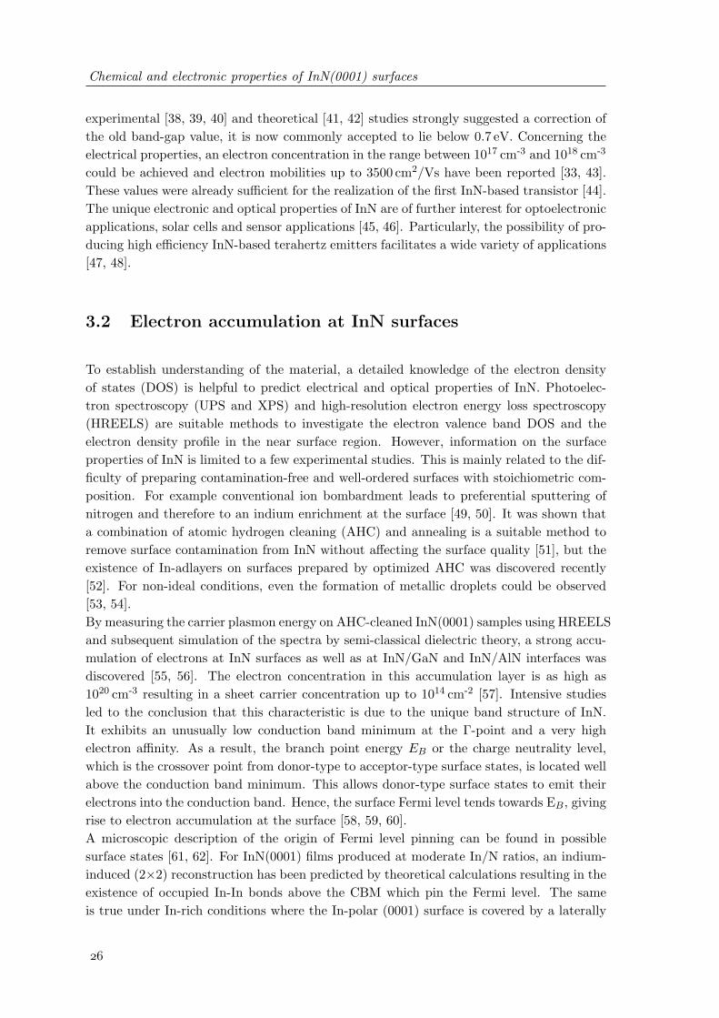
Chemical and electronic properties of InN(0001) surfaces
experimental [38, 39, 40] and theoretical [41, 42] studies strongly suggested a correction ofthe old band-gap value, it is now commonly accepted to lie below 0.7 eV. Concerning theelectrical properties, an electron concentration in the range between 1017 cm-3 and 1018 cm-3
could be achieved and electron mobilities up to 3500 cm2/Vs have been reported [33, 43].These values were already sufficient for the realization of the first InN-based transistor [44].The unique electronic and optical properties of InN are of further interest for optoelectronicapplications, solar cells and sensor applications [45, 46]. Particularly, the possibility of pro-ducing high efficiency InN-based terahertz emitters facilitates a wide variety of applications[47, 48].
3.2 Electron accumulation at InN surfaces
To establish understanding of the material, a detailed knowledge of the electron densityof states (DOS) is helpful to predict electrical and optical properties of InN. Photoelec-tron spectroscopy (UPS and XPS) and high-resolution electron energy loss spectroscopy(HREELS) are suitable methods to investigate the electron valence band DOS and theelectron density profile in the near surface region. However, information on the surfaceproperties of InN is limited to a few experimental studies. This is mainly related to the dif-ficulty of preparing contamination-free and well-ordered surfaces with stoichiometric com-position. For example conventional ion bombardment leads to preferential sputtering ofnitrogen and therefore to an indium enrichment at the surface [49, 50]. It was shown thata combination of atomic hydrogen cleaning (AHC) and annealing is a suitable method toremove surface contamination from InN without affecting the surface quality [51], but theexistence of In-adlayers on surfaces prepared by optimized AHC was discovered recently[52]. For non-ideal conditions, even the formation of metallic droplets could be observed[53, 54].By measuring the carrier plasmon energy on AHC-cleaned InN(0001) samples using HREELSand subsequent simulation of the spectra by semi-classical dielectric theory, a strong accu-mulation of electrons at InN surfaces as well as at InN/GaN and InN/AlN interfaces wasdiscovered [55, 56]. The electron concentration in this accumulation layer is as high as1020 cm-3 resulting in a sheet carrier concentration up to 1014 cm-2 [57]. Intensive studiesled to the conclusion that this characteristic is due to the unique band structure of InN.It exhibits an unusually low conduction band minimum at the Γ-point and a very highelectron affinity. As a result, the branch point energy EB or the charge neutrality level,which is the crossover point from donor-type to acceptor-type surface states, is located wellabove the conduction band minimum. This allows donor-type surface states to emit theirelectrons into the conduction band. Hence, the surface Fermi level tends towards EB, givingrise to electron accumulation at the surface [58, 59, 60].A microscopic description of the origin of Fermi level pinning can be found in possiblesurface states [61, 62]. For InN(0001) films produced at moderate In/N ratios, an indium-induced (2×2) reconstruction has been predicted by theoretical calculations resulting in theexistence of occupied In-In bonds above the CBM which pin the Fermi level. The sameis true under In-rich conditions where the In-polar (0001) surface is covered by a laterally

3.3 Examination of InN surfaces which have been exposed to ambient conditions
contracted In bilayer. At this high coverage, the In-In bonds and dangling-bond statesstrongly interact, leading to a large energy dispersion within the band gap. A similar be-havior is found for nonpolar InN surfaces prepared at In-rich conditions. In contrast, formoderate In/N ratio an absence of occupied states inside the conduction band is predictedon m- and a-plane InN and hence, no electron accumulation would exist when the samplesare prepared under these specific conditions [61, 62]. However, electron accumulation hasbeen found experimentally on m-plane and a-plane as well as cubic InN surfaces [63, 64].The surface electron layer influences the electrical properties of InN films and the complexconsequences of this aspect on the performance of InN-based devices are the topic of ongo-ing research. Crucial will be the open question whether there is a possibility to control thecarrier density in the accumulation layer, which will have strong impact on the switchingbehavior in InN transistors and is also an important parameter for chemical and biologicalsensors applications.
3.3 Examination of InN surfaces which have been exposed
to ambient conditions
The evaluation of surface properties of InN samples that have been transported throughambient conditions is only possible if suitable preparation routines can be employed. Sincea device for atomic hydrogen cleaning was not available at the used surface analysis sys-tem, a different approach was chosen. Samples that have been grown by V. Lebedev in theNitride-MBE system of the Nanotechnology group at ZMN, were, after growth, transferredas quickly as possible through air into the UHV system in order to minimize the expo-sure time to contaminants. Other InN samples as for example from H. Lu and W. J. Schaff(Cornell University) had been stored for longer time in ambient conditions. The subsequentannealing at temperatures below 250C was relatively successful to reduce the amount ofoxygen at the surface. However carbon related contaminants could not be affected by thistreatment. The results of these examinations are published in [34, 65, 66].For samples with a thickness of ∼ 800 nm, where the coalescence of the initially formed is-lands has not been finalized during growth, surface steps could be measured using contact-mode AFM measurements. Fig. 3.1 shows AFM scans performed on one of these samples.The surface consists of an arrangement of homogeneously distributed islands with an av-erage diameter of ∼ 50 nm which has been formed during the intermediate growth state.The islands are not well separated but seem to be connected due to coalescence as can bededuced from the high resolution normal force scan on the right-hand side. The formationof this well-arranged geometry with directly visible surface steps, which are confined withinthe islands, leads to the conclusion that the growth process is strongly influenced by thefact that the adatom surface migration is sufficiently high to allow the formation of regularstepped structures. The measured step height of ∼ 6 A corresponds well with the crystalstructure of InN. This distance is in good agreement with the c lattice parameter of 5.7 Awithin the accuracy of the AFM measurement.A number of different information on the surface chemistry and valence band structure hasbeen obtained by XPS and UPS measurements on these InN samples [34, 65, 66]. This
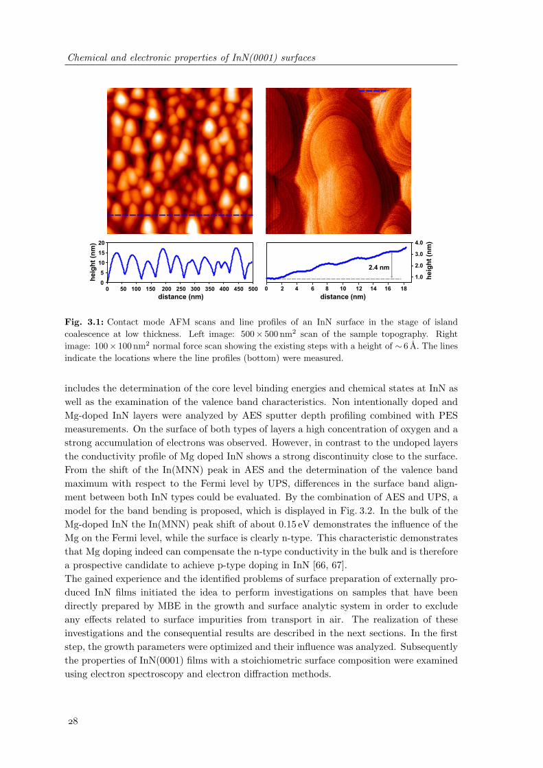
Chemical and electronic properties of InN(0001) surfaces
distance (nm) distance (nm)0 50 100 150 200 250 300 350 400 450 500
0
5
10
15
20
he
igh
t (n
m)
he
igh
t (n
m)
0 2 4 6 8 10 12 14 16 18
4.0
3.0
2.0
1.0
2.4 nm
Fig. 3.1: Contact mode AFM scans and line profiles of an InN surface in the stage of islandcoalescence at low thickness. Left image: 500× 500 nm2 scan of the sample topography. Rightimage: 100× 100 nm2 normal force scan showing the existing steps with a height of ∼ 6 A. The linesindicate the locations where the line profiles (bottom) were measured.
includes the determination of the core level binding energies and chemical states at InN aswell as the examination of the valence band characteristics. Non intentionally doped andMg-doped InN layers were analyzed by AES sputter depth profiling combined with PESmeasurements. On the surface of both types of layers a high concentration of oxygen and astrong accumulation of electrons was observed. However, in contrast to the undoped layersthe conductivity profile of Mg doped InN shows a strong discontinuity close to the surface.From the shift of the In(MNN) peak in AES and the determination of the valence bandmaximum with respect to the Fermi level by UPS, differences in the surface band align-ment between both InN types could be evaluated. By the combination of AES and UPS, amodel for the band bending is proposed, which is displayed in Fig. 3.2. In the bulk of theMg-doped InN the In(MNN) peak shift of about 0.15 eV demonstrates the influence of theMg on the Fermi level, while the surface is clearly n-type. This characteristic demonstratesthat Mg doping indeed can compensate the n-type conductivity in the bulk and is thereforea prospective candidate to achieve p-type doping in InN [66, 67].The gained experience and the identified problems of surface preparation of externally pro-duced InN films initiated the idea to perform investigations on samples that have beendirectly prepared by MBE in the growth and surface analytic system in order to excludeany effects related to surface impurities from transport in air. The realization of theseinvestigations and the consequential results are described in the next sections. In the firststep, the growth parameters were optimized and their influence was analyzed. Subsequentlythe properties of InN(0001) films with a stoichiometric surface composition were examinedusing electron spectroscopy and electron diffraction methods.
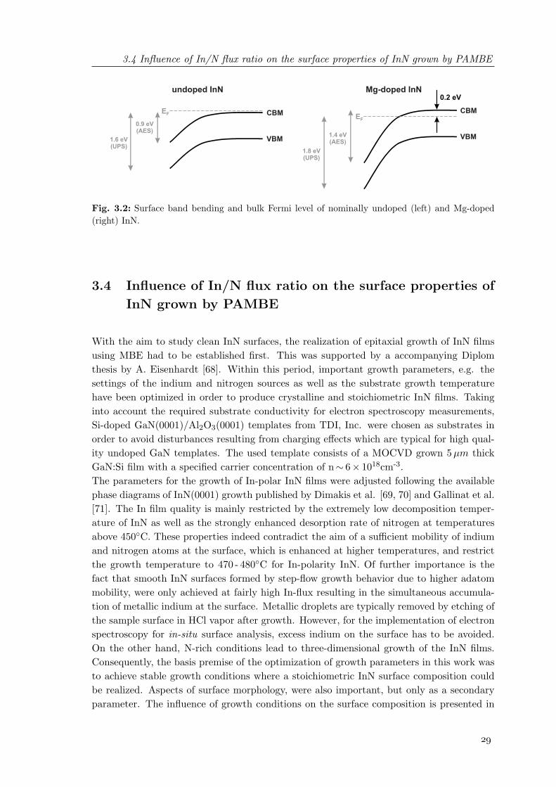
3.4 Influence of In/N flux ratio on the surface properties of InN grown by PAMBE
undoped InN
1.6 eV(UPS)
0.9 eV(AES)
Mg-doped InN
EF CBM
VBM
1.8 eV(UPS)
1.4 eV(AES)
EF
CBM
VBM
0.2 eV
Fig. 3.2: Surface band bending and bulk Fermi level of nominally undoped (left) and Mg-doped(right) InN.
3.4 Influence of In/N flux ratio on the surface properties of
InN grown by PAMBE
With the aim to study clean InN surfaces, the realization of epitaxial growth of InN filmsusing MBE had to be established first. This was supported by a accompanying Diplomthesis by A. Eisenhardt [68]. Within this period, important growth parameters, e.g. thesettings of the indium and nitrogen sources as well as the substrate growth temperaturehave been optimized in order to produce crystalline and stoichiometric InN films. Takinginto account the required substrate conductivity for electron spectroscopy measurements,Si-doped GaN(0001)/Al2O3(0001) templates from TDI, Inc. were chosen as substrates inorder to avoid disturbances resulting from charging effects which are typical for high qual-ity undoped GaN templates. The used template consists of a MOCVD grown 5 µm thickGaN:Si film with a specified carrier concentration of n∼ 6× 1018cm-3.The parameters for the growth of In-polar InN films were adjusted following the availablephase diagrams of InN(0001) growth published by Dimakis et al. [69, 70] and Gallinat et al.[71]. The In film quality is mainly restricted by the extremely low decomposition temper-ature of InN as well as the strongly enhanced desorption rate of nitrogen at temperaturesabove 450C. These properties indeed contradict the aim of a sufficient mobility of indiumand nitrogen atoms at the surface, which is enhanced at higher temperatures, and restrictthe growth temperature to 470 - 480C for In-polarity InN. Of further importance is thefact that smooth InN surfaces formed by step-flow growth behavior due to higher adatommobility, were only achieved at fairly high In-flux resulting in the simultaneous accumula-tion of metallic indium at the surface. Metallic droplets are typically removed by etching ofthe sample surface in HCl vapor after growth. However, for the implementation of electronspectroscopy for in-situ surface analysis, excess indium on the surface has to be avoided.On the other hand, N-rich conditions lead to three-dimensional growth of the InN films.Consequently, the basis premise of the optimization of growth parameters in this work wasto achieve stable growth conditions where a stoichiometric InN surface composition couldbe realized. Aspects of surface morphology, were also important, but only as a secondaryparameter. The influence of growth conditions on the surface composition is presented in
Chemical and electronic properties of InN(0001) surfaces
this section while the subsequent analysis of the surface electronic structure will mainlyfocus on the results for optimized, stoichiometric InN surfaces. Effects of indium accumu-lation on the surface properties of InN films grown at high In/N flux ratio are discussed in[68].The substrate temperature was estimated by linear extrapolation of a pyrometer calibra-tion curve measured at temperatures above 600C. All numbers are given with respect tothis reference. It has to be stated, that this procedure for the specification of temperaturesin the lower region (300 - 500C) leads to a non-negligible error of ± 30 K for the absolutevalues. However, the stability and reproducibility of the performed experiments is com-plied and the error in relative temperature values is below 5 K. Since the flux of reactivenitrogen species to the surface is the limiting factor for the growth rate in the “mini-MBE”system, the settings of the N2 plasma source were chosen to allow stable operation con-ditions but remained unchanged if not otherwise indicated (the nitrogen partial pressurewas 3×10⁻⁵ mbar and the plasma source was operated at 350 W). The main parameters forgrowth optimization were therefore the temperature of the In cell to regulate the metal fluxas well as the substrate temperature which influences the adsorption/desorption balance ofIn and N as well as the mobility of atoms at the surface [71].
T =
75
0°C
74
0°C
72
0°C
InT
=T
=In
In
[ ] [ ]1120 1100
In-r
ich
s
toic
hio
me
tric
N
-ric
h
Fig. 3.3: Variation of the RHEED patterns of InN films deposited with different In/N flux ratioduring PAMBE growth at 440C. Shown are the diffraction patterns along the [1120] and [1100]direction.
Before InN deposition, the GaN templates were heated up to 720C in a nitrogen plasma toremove contaminations from the wafer surface. Special care was taken to avoid roughening

3.4 Influence of In/N flux ratio on the surface properties of InN grown by PAMBE
z-scale: 25 nm z-scale: 15 nm z-scale: 25 nm2x2 2 µm 2
x2 2 µm 2x2 2 µm
N-rich stoichiometric In-rich
T = 720°C 740°C 750°CIn T = T = In In
Fig. 3.4: Dependence of the topography of InN films on the In/N flux ratio during PAMBE growthat 440C measured by non-contact atomic force microscopy.
of the surface which occurs when annealing is performed at slightly higher temperatures.This procedure results in the formation of a sharp (1x1) RHEED pattern and a strongreduction of residual oxygen and carbon impurities at the surface (< 0.2ML) as determinedby XPS. Afterwards, the samples were cooled down to the desired growth temperature,where the InN growth was initiated by opening the shutter of the indium Knudsen cell.The growth was monitored in-situ by RHEED. All produced samples had a relatively lowthickness between 100 and 300 nm, which is related to the relatively low growth rate of20 - 40 nm/h.For a growth temperature of 440C, the influence of the In/N flux ratio on the RHEEDpattern after growth is presented in Fig. 3.3 in a series varying the In evaporator temper-ature as parameter between 720C and 750C. In the following three different stages ofsample stoichiometry resulting from different In-flux settings are compared, denoted “N-rich”, “stoichiometric” and “In-rich” conditions. As expected for the lowest used In flux,the RHEED pattern exhibits a strong contribution from 3-dimensional diffraction spots,a clear indicator for island formation at the surface. The results of the RHEED analysisstands in direct correlation to the sample topography, measured by AFM after growth (seeFig. 3.4). For TIn = 720C, the topography of the sample is relatively rough and charac-terized by the existence of small crystallites with a diameter below 100 nm that are partlyconverged to larger agglomerates. This behavior is typically found for N-rich growth condi-tions [69, 70, 71]. The increase of the indium flux results in an improvement of the RHEEDpattern. The intensity of the transmission spots is strongly reduced and a streaky RHEEDpattern is formed during growth.The pictures in Fig. 3.3 represent the status after growth and subsequent cooling down ofthe samples in the nitrogen plasma. It has to be mentioned that during growth a (1×1)surface structure was always observed. Any additional structures in the RHEED patterns,indicative for the formation of possible surface reconstructions have only been observedafter closing the In-shutter and reducing the sample temperature while the plasma sourcewas still in operation. The nitrogen source was typically switched off at 300 - 250C. Forthe case of TIn =740C, the formation of a (2×2) surface reconstruction is concluded from
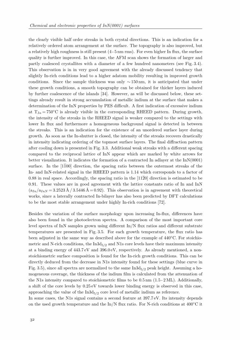
Chemical and electronic properties of InN(0001) surfaces
the clearly visible half order streaks in both crystal directions. This is an indication for arelatively ordered atom arrangement at the surface. The topography is also improved, buta relatively high roughness is still present (4 - 5 nm rms). For even higher In flux, the surfacequality is further improved. In this case, the AFM scan shows the formation of larger andpartly coalesced crystallites with a diameter of a few hundred nanometers (see Fig. 3.4).This observation is in in very good agreement with the already discussed tendency thatslightly In-rich conditions lead to a higher adatom mobility resulting in improved growthconditions. Since the sample thickness was only ∼ 150 nm, it is anticipated that underthese growth conditions, a smooth topography can be obtained for thicker layers inducedby further coalescence of the islands [34]. However, as will be discussed below, these set-tings already result in strong accumulation of metallic indium at the surface that makes adetermination of the InN properties by PES difficult. A first indication of excessive indiumat TIn =750C is already visible in the corresponding RHEED pattern. During growth,the intensity of the streaks in the RHEED signal is weaker compared to the settings withlower In flux and furthermore a homogeneous background signal is detected in betweenthe streaks. This is an indication for the existence of an unordered surface layer duringgrowth. As soon as the In-shutter is closed, the intensity of the streaks recovers drasticallyin intensity indicating ordering of the topmost surface layers. The final diffraction patternafter cooling down is presented in Fig. 3.3. Additional weak streaks with a different spacingcompared to the reciprocal lattice of InN appear which are marked by white arrows forbetter visualization. It indicates the formation of a contracted In adlayer at the InN(0001)surface. In the [1100] direction, the spacing ratio between the outermost streaks of theIn- and InN-related signal in the RHEED pattern is 1.14 which corresponds to a factor of0.88 in real space. Accordingly, the spacing ratio in the [1120] direction is estimated to be0.91. These values are in good agreement with the lattice constants ratio of In and InN(aIn/aInN = 3.2523 A / 3.5446 A = 0.92). This observation is in agreement with theoreticalworks, since a laterally contracted In-bilayer has also been predicted by DFT calculationsto be the most stable arrangement under highly In-rich conditions [72].
Besides the variation of the surface morphology upon increasing In-flux, differences havealso been found in the photoelectron spectra. A comparison of the most important corelevel spectra of InN samples grown using different In/N flux ratios and different substratetemperatures are presented in Fig. 3.5. For each growth temperature, the flux ratio hasbeen adjusted in the same way as described above for the example of 440C. For stoichio-metric and N-rich conditions, the In3d5/2 and N1s core levels have their maximum intensityat a binding energy of 443.7 eV and 396.0 eV, respectively. As already mentioned, a non-stoichiometric surface composition is found for the In-rich growth conditions. This can bedirectly deduced from the decrease in N1s intensity found for these settings (blue curve inFig. 3.5), since all spectra are normalized to the same In3d5/2 peak height. Assuming a ho-mogeneous coverage, the thickness of the indium film is calculated from the attenuation ofthe N1s intensity compared to stoichiometric films to be 0.5 nm (1.5 - 2 ML). Additionally,a shift of the core levels by 0.25 eV towards lower binding energy is observed in this case,approaching the value of the In3d5/2 core level of metallic indium as reference.In some cases, the N1s signal contains a second feature at 397.7 eV. Its intensity dependson the used growth temperature and the In/N flux ratio. For N-rich conditions at 400C it
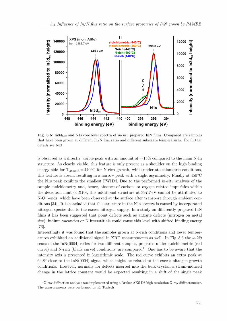
3.4 Influence of In/N flux ratio on the surface properties of InN grown by PAMBE
448 446 444 442 4400
20000
40000
60000
80000
100000
120000
140000
394396398400
0
2000
4000
6000
8000
10000
12000
binding energy (eV)
In3d5/2
N1s
binding energy (eV)
inte
ns
ity
(n
orm
alize
d t
o In
3d
he
igh
t)5/2
XPS (mon. AlK )hν = 1486.7 eV
ástoichiometric (440°C)stoichiometric (450°C)
N-rich (440°C)N-rich (400°C)In-rich (440°C)
inte
ns
ity
(n
orm
alize
d t
o In
3d
he
igh
t)5/2
39
7.7
eV
443.7 eV
396.0 eV
Fig. 3.5: In3d5/2 and N1s core level spectra of in-situ prepared InN films. Compared are samplesthat have been grown at different In/N flux ratio and different substrate temperatures. For furtherdetails see text.
is observed as a directly visible peak with an amount of ∼ 15% compared to the main N-Instructure. As clearly visible, this feature is only present as a shoulder on the high bindingenergy side for Tgrowth =440C for N-rich growth, while under stoichiometric conditions,this feature is absent resulting in a narrow peak with a slight asymmetry. Finally at 450Cthe N1s peak exhibits the smallest FWHM. Due to the performed in-situ analysis of thesample stoichiometry and, hence, absence of carbon- or oxygen-related impurities withinthe detection limit of XPS, this additional structure at 397.7 eV cannot be attributed toN-O bonds, which have been observed at the surface after transport through ambient con-ditions [34]. It is concluded that this structure in the N1s spectra is caused by incorporatednitrogen species due to the excess nitrogen supply. In a study on differently prepared InNfilms it has been suggested that point defects such as antisite defects (nitrogen on metalsite), indium vacancies or N interstitials could cause this level with shifted binding energy[73].Interestingly it was found that the samples grown at N-rich conditions and lower temper-atures exhibited an additional signal in XRD measurements as well. In Fig. 3.6 the ω-2Θscans of the InN(0004) reflex for two different samples, prepared under stoichiometric (redcurve) and N-rich (black curve) conditions, are compared1. One has to be aware that theintensity axis is presented in logarithmic scale. The red curve exhibits an extra peak at64.8 close to the InN(0004) signal which might be related to the excess nitrogen growthconditions. However, normally for defects inserted into the bulk crystal, a strain-inducedchange in the lattice constant would be expected resulting in a shift of the single peak
1X-ray diffraction analysis was implemented using a Bruker AXS D8 high resolution X-ray diffractometer.
The measurements were performed by K. Tonisch
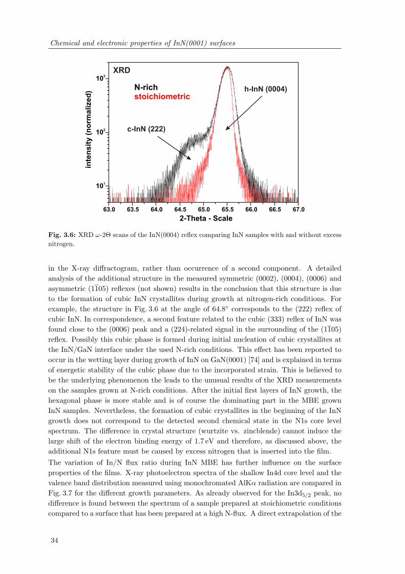
Chemical and electronic properties of InN(0001) surfaces
63.0 63.5 64.0 64.5 65.0 65.5 66.0 66.5 67.0
110
210
310
inte
ns
ity
(n
orm
alize
d)
2-Theta - Scale
h-InN (0004)
XRD
N-richstoichiometric
c-InN (222)
Fig. 3.6: XRD ω-2Θ scans of the InN(0004) reflex comparing InN samples with and without excessnitrogen.
in the X-ray diffractogram, rather than occurrence of a second component. A detailedanalysis of the additional structure in the measured symmetric (0002), (0004), (0006) andasymmetric (1105) reflexes (not shown) results in the conclusion that this structure is dueto the formation of cubic InN crystallites during growth at nitrogen-rich conditions. Forexample, the structure in Fig. 3.6 at the angle of 64.8 corresponds to the (222) reflex ofcubic InN. In correspondence, a second feature related to the cubic (333) reflex of InN wasfound close to the (0006) peak and a (224)-related signal in the surrounding of the (1105)reflex. Possibly this cubic phase is formed during initial nucleation of cubic crystallites atthe InN/GaN interface under the used N-rich conditions. This effect has been reported tooccur in the wetting layer during growth of InN on GaN(0001) [74] and is explained in termsof energetic stability of the cubic phase due to the incorporated strain. This is believed tobe the underlying phenomenon the leads to the unusual results of the XRD measurementson the samples grown at N-rich conditions. After the initial first layers of InN growth, thehexagonal phase is more stable and is of course the dominating part in the MBE grownInN samples. Nevertheless, the formation of cubic crystallites in the beginning of the InNgrowth does not correspond to the detected second chemical state in the N1s core levelspectrum. The difference in crystal structure (wurtzite vs. zincblende) cannot induce thelarge shift of the electron binding energy of 1.7 eV and therefore, as discussed above, theadditional N1s feature must be caused by excess nitrogen that is inserted into the film.The variation of In/N flux ratio during InN MBE has further influence on the surfaceproperties of the films. X-ray photoelectron spectra of the shallow In4d core level and thevalence band distribution measured using monochromated AlKα radiation are compared inFig. 3.7 for the different growth parameters. As already observed for the In3d5/2 peak, nodifference is found between the spectrum of a sample prepared at stoichiometric conditionscompared to a surface that has been prepared at a high N-flux. A direct extrapolation of the
3.4 Influence of In/N flux ratio on the surface properties of InN grown by PAMBE
EF
24 22 20 18 16 14 12 10 8 6 4 2 0 -20
2000
4000
6000
8000
10000
12000
14000
0
100
200
300
400
500
600
700
inte
ns
ity
(n
orm
alize
d t
o In
3d
he
igh
t)5/2
binding energy (eV)
N2sVB
In4d
stoichiometricN-richIn-rich
In metal
x20
XPS (mon. AlK )hν = 1486.7 eV
á
Fig. 3.7: Photoemission spectra of the InN valence band and the In4d and N2s semi-core levelmeasured using monochromated AlKα radiation (hν =1486.7 eV). Presented are measurements offilms that have been deposited under different In/N flux ratio in comparison to metallic In.
valence band trailing edge from the XPS scans leads to a valence band maximum of 1.55 eVbelow the Fermi level EF . This value is in excellent agreement with published data [60] andproves the existence of the electron accumulation layer at contamination-free InN surfaces.MBE growth at slightly indium-rich conditions modifies this behavior. Most noticeably,now strong electron emission is detected up to EF and the N2s and valence band intensity,which mainly consists of N2p states, is reduced. Furthermore, the electronic states areshifted by 0.25 eV towards EF and the In4d spin orbit splitting is well resolved. All thesefeatures can be explained by the existence of excess surface indium under these conditions.To support this statement, an indium reference spectrum is plotted for comparison. It has tobe mentioned that reports exist which contain VB spectra of InN films prepared by atomichydrogen cleaning (AHC) that also show electron emission up to the Fermi level [52]. Thisfeature was explained by the formation of stable indium adlayers with a simulated thicknessof ∼ 3.4ML on top the InN crystal lattice for In-polarity InN. Theoretical calculations alsopredict the stability of metallic adlayer configurations under In-rich conditions [72, 75]. Asimilar origin can be assumed for the results presented here, since no droplet formation wasobserved in the AFM measurements.Using He II radiation to study the valence band and the In4d structure, brings the advantageof being even more surface sensitive. The respective measurements are shown in Fig. 3.8.One has to be aware of some special aspects of these spectra. Since photoelectrons aregenerated by all spectral lines produced by the UV source, several features in the presentedspectra are caused by ghost/satellite lines and do not belong to the actual density of statesof InN at the respective binding energy values. First of all, most of the signal below akinetic energy of 21.2 eV is generated by He I radiation. Furthermore, disturbing signals
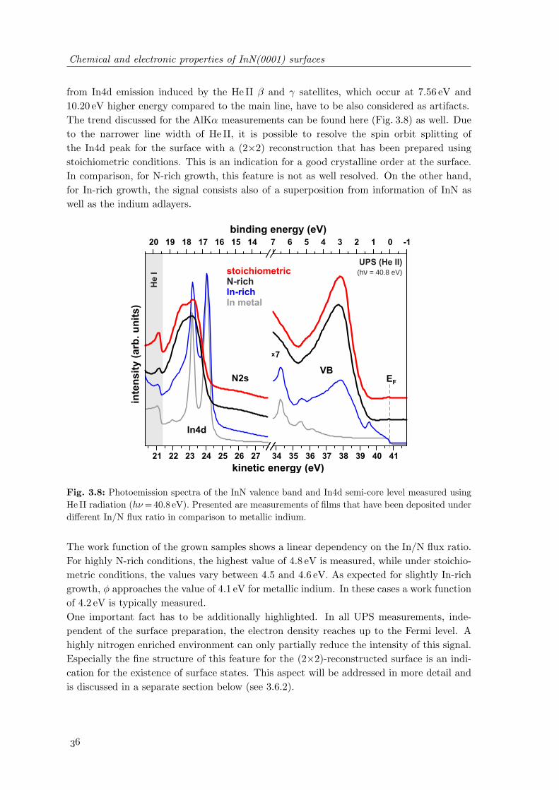
Chemical and electronic properties of InN(0001) surfaces
from In4d emission induced by the He II β and γ satellites, which occur at 7.56 eV and10.20 eV higher energy compared to the main line, have to be also considered as artifacts.The trend discussed for the AlKα measurements can be found here (Fig. 3.8) as well. Dueto the narrower line width of He II, it is possible to resolve the spin orbit splitting ofthe In4d peak for the surface with a (2×2) reconstruction that has been prepared usingstoichiometric conditions. This is an indication for a good crystalline order at the surface.In comparison, for N-rich growth, this feature is not as well resolved. On the other hand,for In-rich growth, the signal consists also of a superposition from information of InN aswell as the indium adlayers.
VBN2s
stoichiometricN-richIn-richIn metal
inte
ns
ity
(a
rb. u
nit
s)
kinetic energy (eV)
x7
In4d
EF
UPS (He II)(hν = 40.8 eV)
21 22 23 24 25 26 27 34 35 36 37 38 39 40 41
20 19 18 17 16 15 14 7 6 5 4 3 2 1 0 -1
binding energy (eV)
He
I
Fig. 3.8: Photoemission spectra of the InN valence band and In4d semi-core level measured usingHe II radiation (hν =40.8 eV). Presented are measurements of films that have been deposited underdifferent In/N flux ratio in comparison to metallic indium.
The work function of the grown samples shows a linear dependency on the In/N flux ratio.For highly N-rich conditions, the highest value of 4.8 eV is measured, while under stoichio-metric conditions, the values vary between 4.5 and 4.6 eV. As expected for slightly In-richgrowth, φ approaches the value of 4.1 eV for metallic indium. In these cases a work functionof 4.2 eV is typically measured.One important fact has to be additionally highlighted. In all UPS measurements, inde-pendent of the surface preparation, the electron density reaches up to the Fermi level. Ahighly nitrogen enriched environment can only partially reduce the intensity of this signal.Especially the fine structure of this feature for the (2×2)-reconstructed surface is an indi-cation for the existence of surface states. This aspect will be addressed in more detail andis discussed in a separate section below (see 3.6.2).
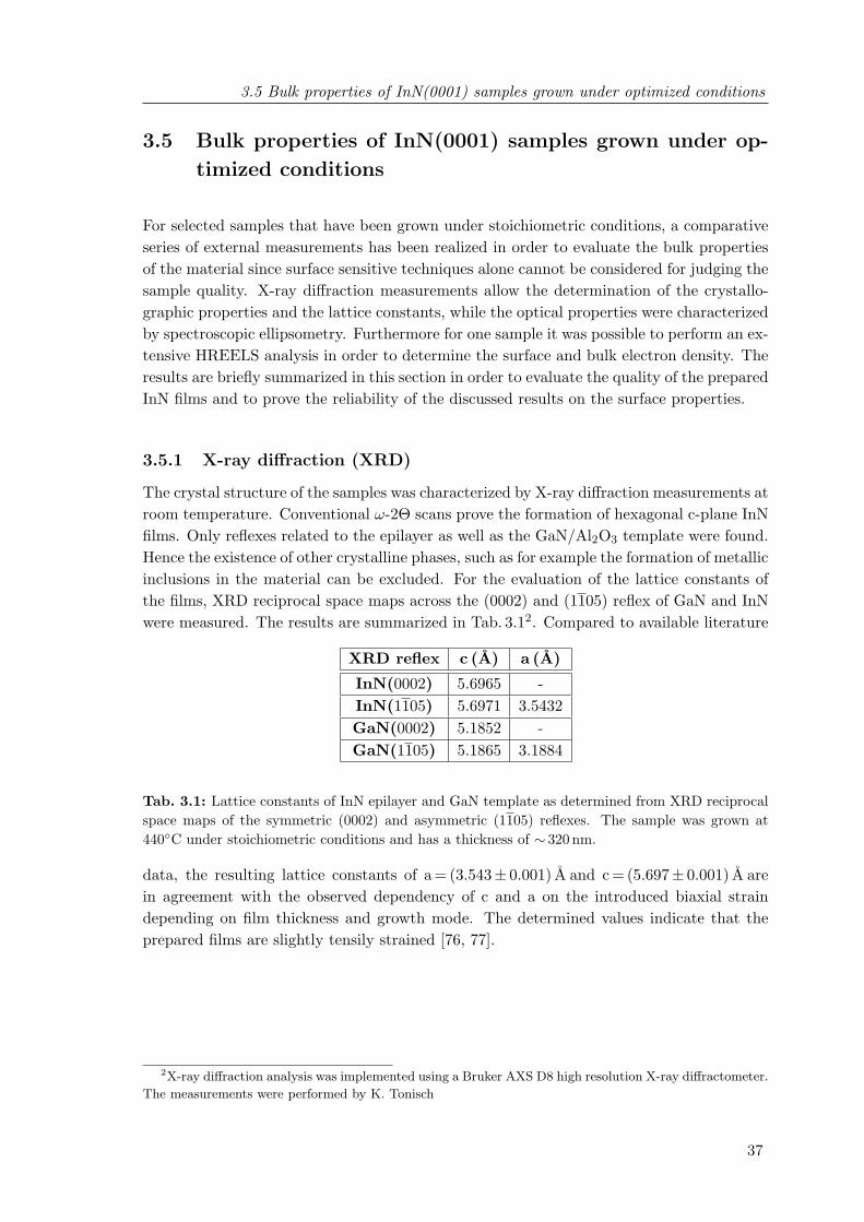
3.5 Bulk properties of InN(0001) samples grown under optimized conditions
3.5 Bulk properties of InN(0001) samples grown under op-
timized conditions
For selected samples that have been grown under stoichiometric conditions, a comparativeseries of external measurements has been realized in order to evaluate the bulk propertiesof the material since surface sensitive techniques alone cannot be considered for judging thesample quality. X-ray diffraction measurements allow the determination of the crystallo-graphic properties and the lattice constants, while the optical properties were characterizedby spectroscopic ellipsometry. Furthermore for one sample it was possible to perform an ex-tensive HREELS analysis in order to determine the surface and bulk electron density. Theresults are briefly summarized in this section in order to evaluate the quality of the preparedInN films and to prove the reliability of the discussed results on the surface properties.
3.5.1 X-ray diffraction (XRD)
The crystal structure of the samples was characterized by X-ray diffraction measurements atroom temperature. Conventional ω-2Θ scans prove the formation of hexagonal c-plane InNfilms. Only reflexes related to the epilayer as well as the GaN/Al2O3 template were found.Hence the existence of other crystalline phases, such as for example the formation of metallicinclusions in the material can be excluded. For the evaluation of the lattice constants ofthe films, XRD reciprocal space maps across the (0002) and (1105) reflex of GaN and InNwere measured. The results are summarized in Tab. 3.12. Compared to available literature
XRD reflex c (A) a (A)
InN(0002) 5.6965 -InN(1105) 5.6971 3.5432GaN(0002) 5.1852 -GaN(1105) 5.1865 3.1884
Tab. 3.1: Lattice constants of InN epilayer and GaN template as determined from XRD reciprocalspace maps of the symmetric (0002) and asymmetric (1105) reflexes. The sample was grown at440C under stoichiometric conditions and has a thickness of ∼ 320 nm.
data, the resulting lattice constants of a = (3.543± 0.001) A and c = (5.697± 0.001) A arein agreement with the observed dependency of c and a on the introduced biaxial straindepending on film thickness and growth mode. The determined values indicate that theprepared films are slightly tensily strained [76, 77].
2X-ray diffraction analysis was implemented using a Bruker AXS D8 high resolution X-ray diffractometer.
The measurements were performed by K. Tonisch

Chemical and electronic properties of InN(0001) surfaces
3.5.2 Spectroscopic ellipsometry (SE)
For the examination of the optical properties of InN films grown at 440C and 450C,samples were hand over to the Experimental Physics I group at TU Ilmenau, which hasextensive experience in the characterization of optical semiconductor properties, especiallyof III-Nitrides. Variable angle spectroscopic ellipsometry was performed in the energyrange from 0.7 eV to 5.0 eV using a commercially available rotating-analyzer ellipsometer(Woollam VASE) at incidence angles of 62, 68 and 74 with respect to the surface normal3.The samples were examined according to their studies on In- and N-polarity hexagonal InNfilms [78]. The real (ε1) and the imaginary part (ε2) of the complex dielectric functionε = ε1 + iε2 were obtained by fitting the experimental data Ψ and ∆ using a multilayermodel similar to the procedure reported in [79]. In that way, the InN film thickness couldbe determined. Taking into account the Burstein-Moss shift and band-gap renormalizationdue to occupancy of the conduction band as well as the intrinsic InN band-gap of 0.68 eV,the bulk carrier concentration can be estimated by a comparison of the calculated shape ofthe imaginary part of the dielectric function with the experimental data (see Fig. 2 in Ref.[78]).For the examined samples, the bulk carrier concentration was estimated to lie between8×1018 cm-3 and 1×1019 cm-3. In comparison to the typical values obtained for MBE grownInN films, this carrier concentration is about one order of magnitude higher. This fact canpartially be explained by the relatively low film thickness (250 - 300 nm) of the produced InNsamples. Normally, the dislocation density as well as the carrier concentration is drasticallylower at a film thickness above 1µm [43]. However, due to the low growth rate of ∼ 20 nm/h,such a thickness of the InN films could not be achieved in a reasonable time with the givensetup.
3.5.3 High-resolution electron energy loss spectroscopy (HREELS)
High-resolution electron energy loss spectroscopy (HREELS) measurements were performedon a sample with a thickness of 320 nm. For this purpose, the as-prepared sample was trans-ferred via a high-vacuum transport box to a second UHV system equipped with a HREELspectrometer. It allows transfer of samples without exceeding a pressure of 1×10⁻⁵ mbarfor approximately 1 hour. In this manner, sample contamination could be minimized en-abling measurements without any further preparation steps. For evaluation of the electrondensity profile inside the InN film, a series of HREEL spectra were measured varying theprimary electron energy E0 from 1 eV to 200 eV. Besides the detected vibrational modessuch as the InN Fuchs-Kliewer phonon at 566 cm-1 (70.2meV) as well as the C-H stretchingand bending modes, the shift of the carrier plasmon could be evaluated. Since the probingdepth for inelastic scattering is inverse proportional to the scattering vector
q‖ =√
2E0me
~· sin(Θ) ·
(1−
√1− EL
E0
)(3.1)
which depends on the used primary energy E0, the respective loss energy EL (the measuredcarrier plasmon energy in this case), the electron mass me and the chosen scattering geome-
3The SE measurements as well as the subsequent modeling were carried out by P. Schley.
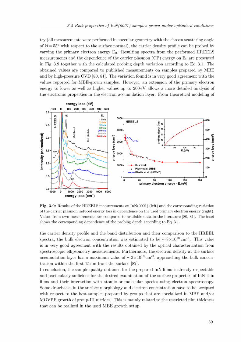
3.5 Bulk properties of InN(0001) samples grown under optimized conditions
try (all measurements were performed in specular geometry with the chosen scattering angleof Θ= 55 with respect to the surface normal), the carrier density profile can be probed byvarying the primary electron energy E0. Resulting spectra from the performed HREELSmeasurements and the dependence of the carrier plasmon (CP) energy on E0 are presentedin Fig. 3.9 together with the calculated probing depth variation according to Eq. 3.1. Theobtained values are compared to published measurements on samples prepared by MBEand by high-pressure CVD [80, 81]. The variation found is in very good agreement with thevalues reported for MBE-grown samples. However, an extension of the primary electronenergy to lower as well as higher values up to 200 eV allows a more detailed analysis ofthe electronic properties in the electron accumulation layer. From theoretical modeling of
inte
ns
ity
(n
orm
alize
d)
-1energy loss (cm )
energy loss (eV)
-1000 0 1000 2000 3000 4000 50000.0
0.5
1.0
1.5
2.0
2.5
3.0-100 0 100 200 300 400 500 600
1.5 eV2.5 eV3.5 eV8.0 eV
20.0 eV80.0 eV
140.0 eV
HR
EE
LS
0 40 80 120 160 200
0
1000
2000
3000
4000
5000
0
100
200
300
400
500
600
-1 e
ne
rgy
lo
ss
(c
m)
this work
Piper et al. (MBE)
Bhatta et al. (HPCVD)
primary electron energy - E (eV)0
en
erg
y lo
ss
(m
eV
)
HREELS
0 50 100 1500
10
20
30
40
E (eV)0
pro
bin
g d
ep
th (
nm
)
C-H
str
etc
h
C-H
be
nd
FK
x10
E0
CP
Fig. 3.9: Results of the HREELS measurements on InN(0001) (left) and the corresponding variationof the carrier plasmon induced energy loss in dependence on the used primary electron energy (right).Values from own measurements are compared to available data in the literature [80, 81]. The insetshows the corresponding dependence of the probing depth according to Eq. 3.1.
the carrier density profile and the band distribution and their comparison to the HREELspectra, the bulk electron concentration was estimated to be ∼ 8×1018 cm-3. This valueis in very good agreement with the results obtained by the optical characterization fromspectroscopic ellipsometry measurements. Furthermore, the electron density at the surfaceaccumulation layer has a maximum value of ∼ 3×1019 cm-3, approaching the bulk concen-tration within the first 15 nm from the surface [82].In conclusion, the sample quality obtained for the prepared InN films is already respectableand particularly sufficient for the desired examination of the surface properties of InN thinfilms and their interaction with atomic or molecular species using electron spectroscopy.Some drawbacks in the surface morphology and electron concentration have to be acceptedwith respect to the best samples prepared by groups that are specialized in MBE and/orMOVPE growth of group-III nitrides. This is mainly related to the restricted film thicknessthat can be realized in the used MBE growth setup.

Chemical and electronic properties of InN(0001) surfaces
3.6 Electronic properties of clean InN(0001) surfaces probed
by electron spectroscopy
In this section, the surface electronic structure of InN samples, that have been producedafter careful optimization of all growth parameters, to assure a clean surface with stoichio-metric composition, are described.
3.6.1 Occupied and unoccupied electronic states
The possibility to investigate several aspects of the density of occupied electron states bymeans of photoelectron spectroscopy has already been presented above. Such investiga-tions have been applied in the past using X-ray photoelectron spectroscopy to support bulkband structure calculations from density functional theory as well as to analyze the effectof downward band bending induced by the formation of the electron accumulation layer[83, 60]. Implementing X-rays, the resulting VB spectra are comparable to the bulk densityof states integrated over the whole Brillouin zone of the material. The first aspect is causedby the fact that the inelastic mean free path of electrons with a kinetic energy around1500 eV is relatively large (between 25 and 30 A). Therefore, the resulting signal consistsof information integrating over several lattice planes. In contrast, the implementation ofultra-violet photoelectron spectroscopy for the examination of the surface valence banddensity of states is strongly restricted to adsorbate-free samples due to the extremely lowelectron inelastic mean free path in this case. Hence, such investigations are strongly linkedto the preparation of the samples and have so far not been satisfactory [49, 65].For a correct interpretation of the PES measurements, one further aspect has to be con-sidered. Since the analyzer electron optics determines the angular acceptance angle ∆Θof the detected electrons, only electrons in a certain range of the wave vector componentparallel to the surface are detected in the normal emission geometry. Hence, the measuredvalence band spectra consist of a summation of electron states in the Brillouin zone aroundthe Γ-point. Depending on the kinetic energy of the emitted electrons and the analyzeracceptance angle, only parts of the whole electron states in the Brillouin zone are accessibleaccording to
k‖, max =√
2Ekinme
~· sin(∆Θ) (3.2)
This dependency is depicted in Fig. 3.10 for the used experimental settings (acceptance an-gle of 8). In the energy range of XPS measurements, the whole Brillouin zone is covered,while for the He I and He II as well as the secondary electron region only states from a cer-tain proportion around the Γ-point are analyzed, which gives a limitation of the performedmeasurements. On the other hand, this aspect enables k-mapping of the occupied electronstates using angle-dependent UPS measurements. However, the above discussed aspectsare only strictly true for perfectly flat single crystal surfaces. Since the investigated InNsamples have a topography with a roughness of 4 - 5 nm, an additional contribution in thephotoelectron spectra is caused by emission of electrons from other crystal directions thanthe c-plane. A quantification of this effect is almost impossible, but in summary it has tobe kept in mind that UPS spectra do not contain information about the whole set of states

3.6 Electronic properties of clean InN(0001) surfaces probed by electron spectroscopy
He IIHe I XPS
1 10 100 1000
0.0
0.2
0.4
0.6
0.8
1.0
1.2
1.4
InN K-point
InN M-point
Γ-point energy above E (eV)Vac
k(1
/)
II
Å8°
4°
1°
unoccupied states occ. s.
Fig. 3.10: k-dependence of the detected electron states in PES for different analyzer acceptanceangles (∆Θ= 1, 4 and 8). For a given electron energy, the information in the PES spectrumincludes information from electron states of a certain k-range (05 k‖ 5 k‖, max).
in the Brillouin zone.In addition to the usually investigated occupied electron states in PES, further informationon unoccupied states can be obtained by the analysis of the fine structure of the secondaryelectron cascade peak. Most of the information on unoccupied states is currently availablefrom ellipsometry measurements [40, 84] and soft X-ray emission/absorption (XES/XAS)experiments [85], which were already compared to results from band structure calculations.For the involved processes, typically the projected partial density of p-like states (p-DOS)has to be considered [84, 85].An example of a complete photoelectron spectrum excited by He I radiation is shown inFig. 3.11. Such spectra normally contain a superposition of information from electrons thathave not suffered any energy loss during movement towards the surface and those whichwere subject of inelastic scattering. Due to the special distribution of the energy levels inInN (the density of states between the In4d level and valence band region is almost zero -see Fig. 3.7), these two contributions can be divided. The region between the abrupt onsetof the secondary cascade peak, which represents the position of the vacuum level EV ac, anda kinetic energy of ∼ 15 eV contains no spectral information of occupied InN states. Sincethe cascade peak of true secondary electrons normally represent a broad and featurelesssignature, as exemplarily indicated in the picture as gray graph, any fine structure is re-lated to electrons that were scattered into unoccupied states above EV ac before exiting thesurface. Since multiple scattering processes are involved, the resulting energetic levels rep-resent states from the complete density of states (s-, p- and d-like). The separation betweenoccupied and unoccupied states for InN can therefore be made by a simple cut through theHe I spectrum as indicated in Fig. 3.11. In that way the information of PES measurementsare expanded to unoccupied states up to ∼ 12 eV above the Fermi level. Unfortunately,since electrons that are scattered into unoccupied states below the vacuum level cannotexit the surface, the region between EF and EV ac is not accessible by PES in this way.For stoichiometric InN(0001) films prepared using the optimized growth conditions, the

Chemical and electronic properties of InN(0001) surfaces
4 6 8 10 12 14 16 18 20 22 24
inte
ns
ity
(a
rb. u
nit
s)
kinetic energy (eV)
UPS (He I)(hν = 21.2 eV)
Bias -2V
occupied states below EF
EF
EV
ac
unoccupied states above EVac
Fig. 3.11: Schematic of the different energy regions in a He I spectrum of InN that contain informa-tion about occupied states below the Fermi level EF as well as unoccupied states above the vacuumlevel EV ac.
whole energetic distribution is presented in Fig. 3.12, including a compilation of the photo-electron spectra obtained using different excitation sources. It consists of occupied electronstates around the shallow In4d core level around -18 eV, well defined structures in the va-lence band between -8 and -1 eV as well as features up to 12 eV above EF . The resultingenergy distribution is compared to published results from DFT calculations of the densityof states from the groups of F. Bechstedt [83] and C.G. Van de Walle [61]. Of great im-portance for the exact determination of the band structure is the correct treatment of theshallow semi-core In4d level whose binding energy is typically underestimated in DFT. Thechoice of the proper functionals is a further aspect for obtaining adequate band structureresults. Typically, the calculated band gap values from DFT are too small and for InN evennegative gaps were calculated. Both groups have achieved a correct determination of theband gap energy, by extensive studies either by using the HSE03 functional [86] or usingmodified pseudopotentials [87].
An overall qualitative agreement is found for the occupied states between the theoreticaland the experimental data presented here, which is also comparable to recently publishedmeasurements [83] (the peak notations in Fig. 3.12 are adopted from this publication). Themeasured width of the valence band is in between the values of the theoretical calcula-tions as can be seen in the energetic location of the structures denoted SWZ
I and PWZII in
Fig. 3.12. As quality indicator, the structure at -5.05 eV (denoted SWZI in [83]) is much bet-
ter pronounced in the UPS measurements. This is due to the better energy resolution andsignal-to-noise ratio for these measurements compared to the XPS results. In contrast tothe slightly overestimated width of the VB calculated using HSE03, the energetic positionof the In4d level together with the N2s contribution is slightly lower if compared to theexperimentally determined values, but it has to be mentioned that the comparison with theexperiments is complicated since e.g. spin orbital splitting of the In4d level is too complexto be implemented in the DFT calculations [88]. However, this effect has a strong influenceon the actual peak shape as visible in the He II spectrum, where the contributions from the

3.6 Electronic properties of clean InN(0001) surfaces probed by electron spectroscopy
bin
din
g e
nerg
y (
eV
) -
E =
0 e
VF
-25
-20
-15
-10
-50
510
15
-20
-15
-10
-50
510
15
N2s
x4
PES intensity (arb. units) InN density of states
x2
0
In4d
not accessible by PES
x1
0
bin
din
g e
nerg
y (
eV
) -
VB
M =
0 e
V
In
N D
OS
(B
ec
hs
ted
t g
rou
p)
sta
tes
at
Γ-
po
int
InN
DO
S (
Va
n d
e W
alle
gro
up
)
XP
S (
AlK
α)U
PS
(H
e II)
UP
S (
He I)
se
co
nd
ary
ele
ctr
on
ca
scad
e
PIIW
ZP
IWZ
SIW
Z
7.2 eV
5.6 eV
9.3 eV
11.2 eV
In4
d3
/2In
4d
5/2
Φ =
4.6
eV
EF
EVac
Fig
.3.
12:
Com
pari
son
ofth
eIn
Nde
nsity
ofoc
cupi
edan
dun
occu
pied
stat
esbe
twee
nav
aila
ble
DFT
calc
ulat
ions
(fro
mth
egr
oups
ofF.B
echs
tedt
[83]
and
C.G
.V
ande
Wal
le[6
1])
and
the
resu
lts
ofph
otoe
mis
sion
spec
tros
copy
.Fo
rth
esi
gnat
ures
ofth
eIn
4dle
velan
dth
eva
lenc
eba
nddi
stri
buti
on,a
Shir
ley-
type
back
grou
ndha
sbe
ensu
btra
cted
from
the
mea
sure
dsp
ectr
a.
Chemical and electronic properties of InN(0001) surfaces
In4d3/2 and In4d5/2 electrons are clearly separated.The comparison of the calculated unoccupied electron states is more complicated, since thestructures in the secondary electron signal are partially only visible as weak shoulders. Nev-ertheless, features with an energy of 5.6 eV, 7.2 eV, 9.3 eV and 11.2 eV above EF could beidentified in the measurement. These states do not agree very well with the position of theelectronic states in the above plotted theoretical data in Fig. 3.12. A direct comparison isdifficult, since the aspects of not detecting all electron states from the whole Brillouin zoneplays an important role in that case. Therefore, the calculated energy states at the Γ-pointare included in addition. It seems that a qualitative agreement could be achieved if oneregards the states in the measurement to be shifted to higher energy values by about 1 eV.A comparable shift between the theoretical data and experimental results was also found inXAS/XES experiments and was there assigned to final state effects, such as the measuredelectron is bound in an exciton [85]. Final state relaxation effects due to the formation ofcore-holes can indeed cause a shift of the measured energy values of core electrons in PES.However, for the process of scattering of slow electrons into unoccupied states above EV ac,such a strong shift is not expected. Since possible explanations are only speculative, it hasto be stated that the difference between the calculated DOS of unoccupied states and themeasurements from photon-induced secondary electron emission are not well understood atthe moment, but matter of further investigations.
3.6.2 InN(0001)-(2×2) and -(√
3×√
3)R30 surface states
Adequate procedures to prepare well ordered and stoichiometric InN surfaces are ratherrare. Most of the studies of the InN electronic structure are performed on samples witha (1×1) diffraction pattern. On the other hand, documented surface reconstructions ofIn-polarity InN are limited to in-situ RHEED measurements during growth. So far a(√
3×√
3)R30 reconstruction has been reported to exist on InN(0001) [89, 52]. From ionscattering and PES measurements it was concluded that this reconstruction is related tothe formation of metallic indium adlayers at the InN(0001) surface due to In-rich growthconditions. Indeed, the formation of In-adlayers has also been predicted by density func-tional theory calculations to be stable in that case [75, 72].For the experiments performed on InN(0001), two surface reconstruction could be detectedfor specially adapted preparation conditions. Fig. 3.13 contains the RHEED patterns alongthe [1120] and [1100] directions for these two cases. The two top images represent thealready mentioned (2×2) superstructure with half order streaks in both directions. Thisreconstruction was observed for the optimized In/N flux ratio at the following growthparameters: pnitrogen = 3×10⁻⁵ mbar, P= 350W, Tgrowth =440C. For experiments thataimed the achievement of slightly higher growth rates, different growth conditions werechosen. Since the growth rate of the used MBE system is mainly restricted by the lownitrogen flux, the parameters of the plasma source were set to higher, but still stable condi-tions (pnitrogen =7×10⁻⁵ mbar, P= 450 W) in order to achieve the maximum flux of reactivenitrogen towards the surface. At the same time, a slightly higher growth temperature of450C had been chosen. The growth parameters were adjusted in order to obtain stoichio-metric InN surfaces as judged from XPS and UPS measurements following the same routine
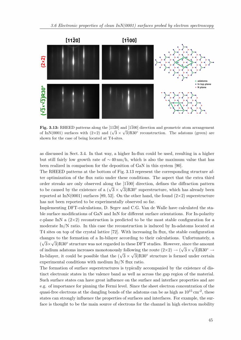
3.6 Electronic properties of clean InN(0001) surfaces probed by electron spectroscopy
[ ] [ ]1120 1100x
(22
)x
(
33)R
30
°
adatoms
In top plane
N plane
Fig. 3.13: RHEED patterns along the [1120] and [1100] direction and geometric atom arrangementof InN(0001) surfaces with (2×2) and (
√3 ×
√3)R30 reconstruction. The adatoms (green) are
shown for the case of being located at T4-sites.
as discussed in Sect. 3.4. In that way, a higher In-flux could be used, resulting in a higherbut still fairly low growth rate of ∼ 40 nm/h, which is also the maximum value that hasbeen realized in comparison for the deposition of GaN in this system [90].The RHEED patterns at the bottom of Fig. 3.13 represent the corresponding structure af-ter optimization of the flux ratio under these conditions. The aspect that the extra thirdorder streaks are only observed along the [1100] direction, defines the diffraction patternto be caused by the existence of a (
√3×
√3)R30 superstructure, which has already been
reported at InN(0001) surfaces [89, 52]. On the other hand, the found (2×2) superstructurehas not been reported to be experimentally observed so far.Implementing DFT-calculations, D. Segev and C.G. Van de Walle have calculated the sta-ble surface modifications of GaN and InN for different surface orientations. For In-polarityc-plane InN a (2×2) reconstruction is predicted to be the most stable configuration for amoderate In/N ratio. In this case the reconstruction is induced by In-adatoms located atT4 sites on top of the crystal lattice [72]. With increasing In flux, the stable configurationchanges to the formation of a In-bilayer according to their calculations. Unfortunately, a(√
3×√
3)R30 structure was not regarded in these DFT studies. However, since the amountof indium adatoms increases monotonously following the route (2×2) → (
√3×
√3)R30 →
In-bilayer, it could be possible that the (√
3 ×√
3)R30 structure is formed under certainexperimental conditions with medium In/N flux ratio.The formation of surface superstructures is typically accompanied by the existence of dis-tinct electronic states in the valence band as well as across the gap region of the material.Such surface states can have great influence on the surface and interface properties and aree.g. of importance for pinning the Fermi level. Since the sheet electron concentration of thequasi-free electrons at the dangling bonds of the adatoms can be as high as 1015 cm-2, thesestates can strongly influence the properties of surfaces and interfaces. For example, the sur-face is thought to be the main source of electrons for the channel in high electron mobility
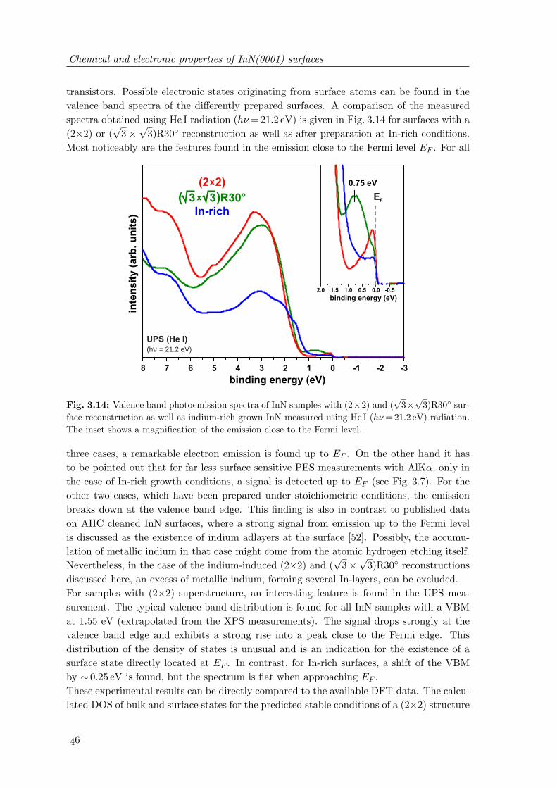
Chemical and electronic properties of InN(0001) surfaces
transistors. Possible electronic states originating from surface atoms can be found in thevalence band spectra of the differently prepared surfaces. A comparison of the measuredspectra obtained using He I radiation (hν = 21.2 eV) is given in Fig. 3.14 for surfaces with a(2×2) or (
√3 ×
√3)R30 reconstruction as well as after preparation at In-rich conditions.
Most noticeably are the features found in the emission close to the Fermi level EF . For all
8 7 6 5 4 3 2 1 0 -1 -2 -3
2.0 1.5 1.0 0.5 0.0 -0.5
inte
ns
ity
(a
rb. u
nit
s)
binding energy (eV)
0.75 eV
EF
binding energy (eV)
x(2 2)
x ( 3 3)R30°In-rich
UPS (He I)(hν = 21.2 eV)
Fig. 3.14: Valence band photoemission spectra of InN samples with (2×2) and (√
3×√
3)R30 sur-face reconstruction as well as indium-rich grown InN measured using He I (hν =21.2 eV) radiation.The inset shows a magnification of the emission close to the Fermi level.
three cases, a remarkable electron emission is found up to EF . On the other hand it hasto be pointed out that for far less surface sensitive PES measurements with AlKα, only inthe case of In-rich growth conditions, a signal is detected up to EF (see Fig. 3.7). For theother two cases, which have been prepared under stoichiometric conditions, the emissionbreaks down at the valence band edge. This finding is also in contrast to published dataon AHC cleaned InN surfaces, where a strong signal from emission up to the Fermi levelis discussed as the existence of indium adlayers at the surface [52]. Possibly, the accumu-lation of metallic indium in that case might come from the atomic hydrogen etching itself.Nevertheless, in the case of the indium-induced (2×2) and (
√3×
√3)R30 reconstructions
discussed here, an excess of metallic indium, forming several In-layers, can be excluded.For samples with (2×2) superstructure, an interesting feature is found in the UPS mea-surement. The typical valence band distribution is found for all InN samples with a VBMat 1.55 eV (extrapolated from the XPS measurements). The signal drops strongly at thevalence band edge and exhibits a strong rise into a peak close to the Fermi edge. Thisdistribution of the density of states is unusual and is an indication for the existence of asurface state directly located at EF . In contrast, for In-rich surfaces, a shift of the VBMby ∼ 0.25 eV is found, but the spectrum is flat when approaching EF .These experimental results can be directly compared to the available DFT-data. The calcu-lated DOS of bulk and surface states for the predicted stable conditions of a (2×2) structure
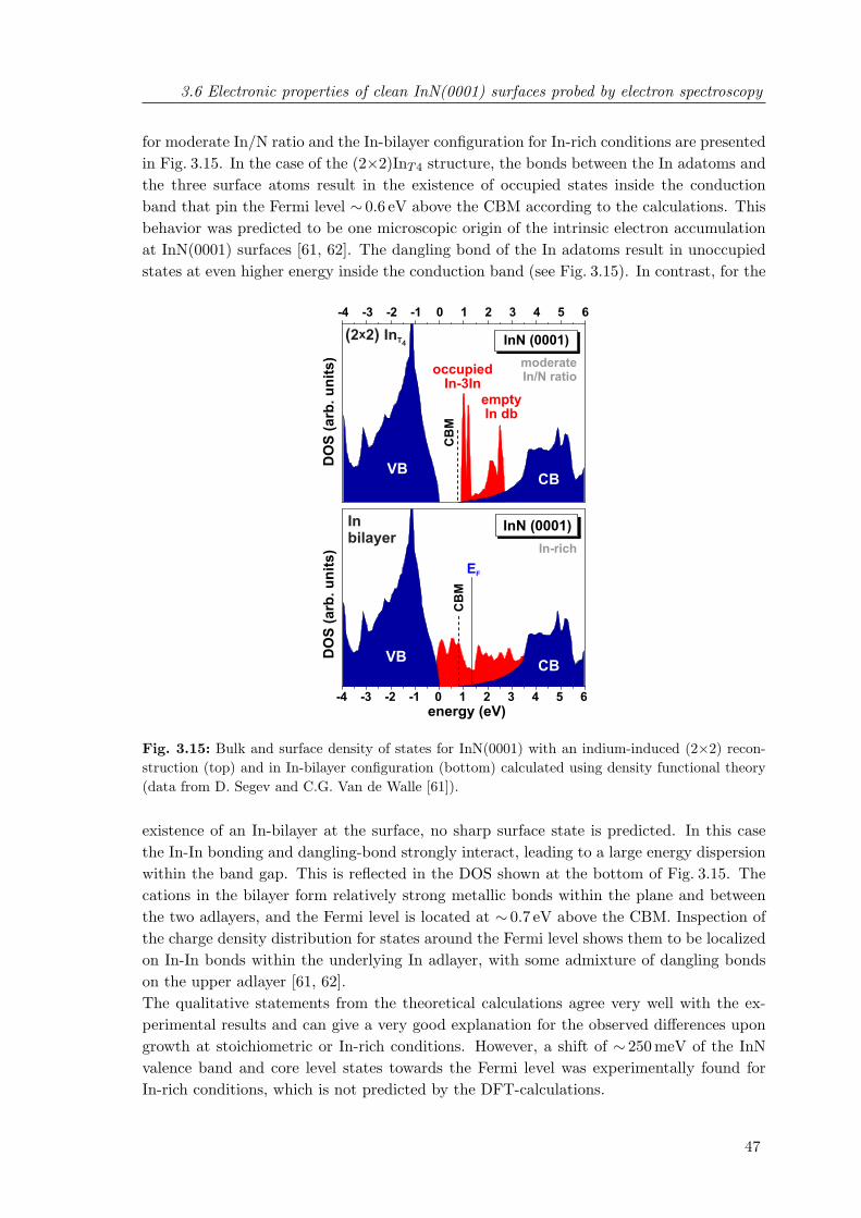
3.6 Electronic properties of clean InN(0001) surfaces probed by electron spectroscopy
for moderate In/N ratio and the In-bilayer configuration for In-rich conditions are presentedin Fig. 3.15. In the case of the (2×2)InT4 structure, the bonds between the In adatoms andthe three surface atoms result in the existence of occupied states inside the conductionband that pin the Fermi level ∼ 0.6 eV above the CBM according to the calculations. Thisbehavior was predicted to be one microscopic origin of the intrinsic electron accumulationat InN(0001) surfaces [61, 62]. The dangling bond of the In adatoms result in unoccupiedstates at even higher energy inside the conduction band (see Fig. 3.15). In contrast, for the
-4 -3 -2 -1 0 1 2 3 4 5 6
-4 -3 -2 -1 0 1 2 3 4 5 6
emptyIn db
CB
M
CB
occupiedIn-3In
DO
S (
arb
. u
nit
s)
D
OS
(a
rb. u
nit
s)
VB
InN (0001)
EF
InN (0001)
CB
energy (eV)
VB
CB
M
moderate In/N ratio
In-rich
x(2 2) InT4
In bilayer
Fig. 3.15: Bulk and surface density of states for InN(0001) with an indium-induced (2×2) recon-struction (top) and in In-bilayer configuration (bottom) calculated using density functional theory(data from D. Segev and C.G. Van de Walle [61]).
existence of an In-bilayer at the surface, no sharp surface state is predicted. In this casethe In-In bonding and dangling-bond strongly interact, leading to a large energy dispersionwithin the band gap. This is reflected in the DOS shown at the bottom of Fig. 3.15. Thecations in the bilayer form relatively strong metallic bonds within the plane and betweenthe two adlayers, and the Fermi level is located at ∼ 0.7 eV above the CBM. Inspection ofthe charge density distribution for states around the Fermi level shows them to be localizedon In-In bonds within the underlying In adlayer, with some admixture of dangling bondson the upper adlayer [61, 62].The qualitative statements from the theoretical calculations agree very well with the ex-perimental results and can give a very good explanation for the observed differences upongrowth at stoichiometric or In-rich conditions. However, a shift of ∼ 250 meV of the InNvalence band and core level states towards the Fermi level was experimentally found forIn-rich conditions, which is not predicted by the DFT-calculations.

Chemical and electronic properties of InN(0001) surfaces
For the experimentally observed (√
3×√
3)R30 reconstruction, distinct states are found atother energy values. As can bee seen in Fig. 3.14, a strong peak is detected 0.75 eV belowEF . For that case no theoretical calculations on surface states are available at present, butit is anticipated that the detected feature is most likely also related to the In-In bonds ofthe adatoms to the three In surface atoms. Due to the higher adatom density and differentarrangement compared to the (2×2) structure, they might be slightly shifted in energy.There is a second feature around 1.6 eV visible as a slight shoulder in the spectrum (green)compared to the other cases. Whether this is caused by a second surface state or is ratherrelated to the bulk valence band emission cannot be clarified at the moment. However, itis believed that the (
√3 ×
√3)R30 superstructure is directly formed on top of the last
plane of indium atoms for the surface preparation used in this case. For the here presentedresults, the spectral signatures in all measured XPS and UPS spectra disagree with theproposed 3 layers of metallic indium forming the (
√3 ×
√3)R30 reconstruction, as has
been suggested for AHC treated films [91].Since the experimental results for the InN(0001) surfaces agree very well with the predic-tions from DFT-calculations, one important perspective has to be mentioned. Evidencefor the existence of an electron accumulation layer at nonpolar surfaces [63, 64] has beenalready experimentally found, which is also predicted from theory for In-rich growth con-ditions. On the other hand, in the cases of m- or a-plane oriented InN films produced atmoderate In/N ratio, there is a chance that occupied electron states are absent inside theconduction band and hence electron accumulation might not occur in this case according totheoretical predictions [61, 62]. Whether this aspect can also be experimentally confirmedwill be the subject of upcoming studies in the near future. Nevertheless, this might be dif-ficult since other donor-type electron states, preferably related to crystal imperfections orimpurities can also act as electron source and can emit their electrons into the conductionband due to the unusual location of the branch point energy in InN [60].
3.6.3 Interaction of InN(0001) with oxygen
Besides the knowledge of the electronic properties of clean surfaces, changes upon interac-tion with other atoms and/or molecules are of great importance. Mainly, the initial stagesof surface modification play the most important role. First experiments were initiated tostudy the oxidation of InN(0001) surfaces using well defined starting conditions. As-grownInN films were exposed to different amounts of molecular oxygen. Upon exposure to 250 Lduring in-situ measurements in the surface analysis chamber, only slight changes were de-tected. Therefore, a significantly higher oxygen exposure was realized by venting the loadlock chamber with pure oxygen while the sample was stored therein. Fig. 3.16 summarizesthe results of the characterization of the valence band states upon interaction with O2. Twostructures appear in the valence band at 5.2 and 10.3 eV. This supports the interpretationof the results discussed in an earlier publication [65], where the spectral features could notbe separated into oxygen states and hydrocarbon related structures. Hence, impurity-freepreconditions allow a doubtless assignment of these features to oxygen adsorbates. As willbe shown in the next chapter, the same adsorbate-induced states are found for the interac-tion of indium oxide surfaces with oxygen-containing molecules, such as O2, O3 and H2O.

3.6 Electronic properties of clean InN(0001) surfaces probed by electron spectroscopy
02468101214161820
5.1 eV
binding energy (eV)
saturated with O 2
250 L O2
as grown
UPS (He II)(hν = 40.8 eV)
UPS (He II)(hν = 40.8 eV)
UPS (He I)(hν = 21.2 eV)
inte
ns
ity
(a
rb. u
nit
s)
5.2 eV
10
.3 e
V
Fig. 3.16: Changes in valence band spectra of InN(0001) upon interaction with O2. The measure-ments were performed using He I and He II radiation.
It is believed that the adsorption of oxygen takes place by a dissociation of the O2 moleculeand bonding of atomic oxygen at indium atoms.Theoretical studies on the energy dependence of different adsorption sites are rarely re-ported. For the InN(0001) surface, calculations predict the T4 site to be the most stablefor adsorption of oxygen or carbon [92]. Unfortunately, no reports can be found for In-polarity InN.As a second aspect, exposure of the clean InN surfaces to oxygen leads to the vanishingof the emission due to the surface states close to the Fermi edge as well as the surfacereconstruction. Hence, the initial adsorption of oxygen atoms is linked to the reaction atthe In-adatoms. Surprisingly, the interaction with oxygen has only minor influence on theenergetic position of the valence band maximum and the core level states as well as thework function of the sample (φ increases by 0.1 eV). Furthermore only a minor influence ofthe interaction with O2 on the core levels is detected.Finally it can be stated, that the sample quality achieved is suitable for surface reac-tion studies which have been preliminary demonstrated for the case of oxygen interaction.Possible further measurements will address the interaction with other oxygen-containingmolecules (for example water) or organic molecules as well as alkali metals. Of furtherrelevance will be studies on the electronic band alignment properties of InN interfaces withpossible gate materials for transistor applications, e.g. the In2O3/InN interface.In further measurements, a strong oxidation by reaction of the InN surfaces with ozone wasobserved. Investigation of the surfaces properties on InN samples that were exposed to O3
has so far only been possible on contaminated samples. However, the formation of a thinindium oxide layer could be detected which results in the variation of the electron transportproperties in the material. The details and results of these experiments are published in[93] and will not be discussed in detail here.

Chemical and electronic properties of InN(0001) surfaces
In summary, implementation of in-situ surface analyses of InN thin films has been realizedfor the first time. Although, the thermodynamic properties of the In-N system are not verysuitable for MBE growth and subsequent surface analysis, since better crystalline qualityis typically achieved at In-rich conditions, a sufficient sample quality of the thin InN filmswas attained. The influences of different growth parameters on the surface compositionand possible excess atoms was studied without having disturbing contribution from expo-sure of the samples to ambient conditions. By the successful preparation of stoichiometricand contamination-free surfaces, it was possible to study the electronic properties of InNincluding the consequences of stable surface reconstructions on electronic states above thevalence band maximum. Surface states were found to exist for the observed (2×2) and(√
3 ×√
3)R30 reconstructions of In-polarity InN films. From this starting base, manyinteresting aspects can be studied in future experiments. For example, the interaction withreactive species has been demonstrated by preliminary oxidation experiments.Nevertheless, it is important to note that the interpretation of the experimental data isonly possible with a strong support from theoretical calculations. So far, only a few workson pure InN surfaces are available and especially data for the interaction with adsorbatesis missing.
Chapter 4
Surface properties and ozone
interaction of indium oxide films
grown by MOCVD
4.1 Indium oxide - an ozone sensitive material at room tem-
perature
Metal oxide films are widely used for sensor applications to measure the concentration ofenvironmental and hazardous gases. Both, oxidizing and reducing species can be detecteddepending on the properties of the used material and the actual operation conditions [94].One important class of these sensors is based on the variation of the film conductivity uponinteraction with atoms or molecules. Prominent representatives of this group of materialsare transparent conductive oxides (TCOs) such as SnO2, ZnO, TiO2 and In2O3, which be-long to the wide band gap materials. Typically the changes in conductivity upon oxidationor reduction can have two different contributions: i) change of the bulk carrier concentra-tion by formation or annihilation of intrinsic dopants and ii) variation of the surface bandbending induced by chemisorption of surface species or reaction of gases with adsorbedspecies [95]. The surface band bending changes result in the alteration of the charge carrierprofile at the surface and induce the formation of energy barriers at grain boundaries inpolycrystalline materials. The complex connections between material properties, devicerelated technological aspects and the gas interaction processes are composed in a compre-hensive overview article on metal oxide based gas sensors [96].The capability of indium oxide films to detect ozone has already been reported in the 80’s[94]. Since then, many different approaches have been followed to tailor the material prop-erties by different synthesis methods, such as RF sputtering or sol-gel processes to improvethe sensitivity of the films towards O3 [97, 98, 99, 100]. Of special importance for thispurpose is the realization of defect-rich In2O3−x films with a high concentration of oxygenvacancies. It has been found that especially indium oxide nanoparticles and nanowires pos-sess a very high sensitivity for the detection of ozone.Most solid gas sensors require temperatures between 200 and 600C in order to reach theiroptimal performance. This is normally realized by passive heating of the sensor device or by

Surface properties and ozone interaction of indium oxide films grown by MOCVD
current induced self-heating during operation. Both principles rely on a relatively high en-ergy consumption since electric power is required for heating. On the other hand, In2O3−x
films can be implemented in ozone sensors operating at room temperature [98, 100]. Thismakes indium oxide based gas sensors very promising for the realization of low energy-consumption and low-cost devices. The regeneration of the material after oxidation is inthis case not engendered by thermal desorption, but realized by illumination of the activesensor area by UV light from a LED. The straightforward layout of such a sensor structureis demonstrated in Fig. 4.1. The O3 concentration is determined via measurement of theincrease in film resistance upon ozone-induced oxidation of the In2O3−x layer. For thin
IU
Al O2 3
indium oxide
nickel contacts
UV-LED λ=375 nmO3
AlN10 20 30 40 50 60 70
510
610
710
810
910
1010
re
sis
tan
ce
(Ù
)
O3
UV
10
.4 p
pm
2.2
5 p
pm
82
0 p
pb
24
0 p
pb
15
pp
b
time (min)
Fig. 4.1: Room temperature ozone detectors based on polycrystalline indium oxide. (left image:schematic of the sensor layout, right image: dependence of the film resistance on the ozone con-centration and illumination with UV light for a ∼ 80 nm nanoparticle layer grown at a substratetemperature of 200C (data from Ch.Y. Wang [100]).
nanocrystalline indium oxide films prepared by MOCVD, ozone concentrations as low as 15parts per billion (ppb) can be detected [100]. The signal response at room temperature todifferent concentrations of O3 is exemplarily depicted in the right part of Fig. 4.1. A devicesensitivity (Rozone/RUV ) > 105 could be realized and the response time was as low as 1 s for10 nm thick films. The film resistance can be reproducibly regenerated by the illuminationwith UV light. This is one key aspect for practical use in reliable and long-term stable ozonesensors. Furthermore, the operation at room temperature assures a low interference fromreducing gases and hence low cross-sensitivity. Nevertheless, for operation temperaturesabove 150C, In2O3−x films have been found to be also sensitive to other gases such as H2,NOx, CO, NH3, CH4 and C2H5OH [101, 102, 103, 104, 105].The surface properties of different metal oxides as well as adsorption of many atomic andmolecular reactive species have already been extensively studied during the last decades[106, 107]. Among the variety of the many functional metal oxides, TiO2 is one of the inmost detail investigated material [108]. It is generally accepted that TiO2 is more bulksensitive, i.e. it exhibits conductivity changes due to variations in intrinsic dopants as aconsequence of the formation of oxygen vacancies and Ti interstitials, while SnO2 and ZnOare considered as surface sensitive materials. In the case of surface sensitive oxides forthe detection of oxidizing and reducing gases, the adsorption of charged surface oxygenspecies plays a central role [95]. Most of the known surface investigations of In2O3 have
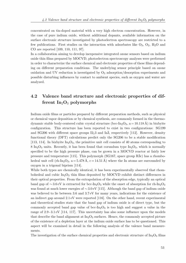
4.2 Valence band structure and electronic properties of different In2O3 polymorphs
concentrated on tin-doped material with a very high electron concentration. However, inthe case of pure indium oxide, without additional dopants, available information on thesurface electronic structure investigated by photoelectron spectroscopy are restricted to afew publications. First studies on the interaction with adsorbates like O3, O2, H2O andCO are reported [109, 110, 111, 97].In a collaboration aiming to develop inexpensive integrated ozone sensors based on indiumoxide thin films prepared by MOCVD, photoelectron spectroscopy analyses were performedin order to characterize the surface chemical and electronic properties of these films depend-ing on different preparation conditions. The underlying sensor principle based on ozoneoxidation and UV reduction is investigated by O3 adsorption/desorption experiments andpossible disturbing influences by contact to ambient species, such as oxygen and water areanalyzed.
4.2 Valence band structure and electronic properties of dif-
ferent In2O3 polymorphs
Indium oxide films or particles prepared by different preparation methods, such as physicalor chemical vapor deposition or by chemical synthesis, are commonly formed in the thermo-dynamic stable body-centered cubic crystal structure (bcc-In2O3, a = 10.118 A) in bixbyiteconfiguration. This structure has been reported to exist in two configurations: SG199and SG206 with different space groups I213 and Ia3, respectively [112]. However, densityfunctional theory (DFT) calculations predict only the SG206 to be a stable modification[113, 114]. In bixbyite In2O3, the primitive unit cell consists of 40 atoms corresponding to8 In2O3 units. Recently, it has been found that corundum type In2O3, which is normallyspecified to be the high pressure phase, can be grown in a MOCVD reactor at fairly lowpressure and temperature [115]. This polymorph (SG167, space group R3c) has a rhombo-hedral unit cell (rh-In2O3, a= 5.478 A, c = 14.51 A) where the In atoms are surrounded byoxygen in a trigonal biprism [114].While both types are chemically identical, it has been experimentally observed that rhom-bohedral and cubic In2O3 thin films deposited by MOCVD exhibit distinct differences intheir optical properties. From the extrapolation of the absorption edge, typically an opticalband gap of ∼ 3.6 eV is extracted for bcc-In2O3 while the onset of absorption for rh-In2O3
was found at much lower energies of ∼ 3.0 eV [115]. Although the band gap of indium oxidewas believed to lie between 3.6 and 3.7 eV for many years, indications for the existence ofan indirect gap around 2.1 eV were reported [116]. On the other hand, recent experimentaland theoretical studies state that the band gap of indium oxide is of direct type, but thecommonly accepted band gap value of bcc-In2O3 is too high and suggest a value in therange of 2.9 - 3.1 eV [114, 117]. This uncertainty has also some influence upon the modelsthat describe the band alignment at In2O3 surfaces. Hence, the commonly accepted pictureof the existence of a depletion layer at the indium oxide surface has to be questioned. Thisaspect will be examined in detail in the following analysis of the valence band measure-ments.The investigation of the surface chemical properties and electronic structure of In2O3 films
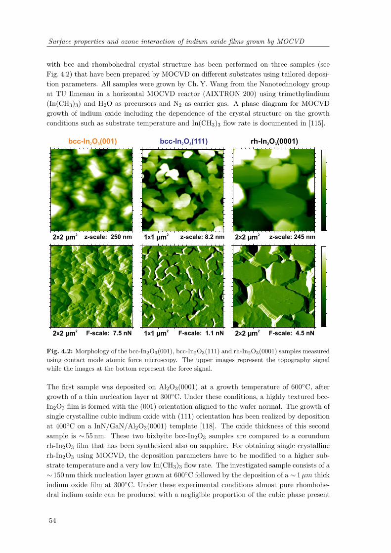
Surface properties and ozone interaction of indium oxide films grown by MOCVD
with bcc and rhombohedral crystal structure has been performed on three samples (seeFig. 4.2) that have been prepared by MOCVD on different substrates using tailored deposi-tion parameters. All samples were grown by Ch. Y. Wang from the Nanotechnology groupat TU Ilmenau in a horizontal MOCVD reactor (AIXTRON 200) using trimethylindium(In(CH3)3) and H2O as precursors and N2 as carrier gas. A phase diagram for MOCVDgrowth of indium oxide including the dependence of the crystal structure on the growthconditions such as substrate temperature and In(CH3)3 flow rate is documented in [115].
z-scale: 250 nm z-scale: 8.2 nm z-scale: 245 nm2x2 2 µm 2
x1 1 µm 2x2 2 µm
bcc-In O (001)2 3 bcc-In O (111) 2 3 rh-In O (0001)2 3
F-scale: 7.5 nN F-scale: 1.1 nN F-scale: 4.5 nN2x2 2 µm 2
x1 1 µm 2x2 2 µm
Fig. 4.2: Morphology of the bcc-In2O3(001), bcc-In2O3(111) and rh-In2O3(0001) samples measuredusing contact mode atomic force microscopy. The upper images represent the topography signalwhile the images at the bottom represent the force signal.
The first sample was deposited on Al2O3(0001) at a growth temperature of 600C, aftergrowth of a thin nucleation layer at 300C. Under these conditions, a highly textured bcc-In2O3 film is formed with the (001) orientation aligned to the wafer normal. The growth ofsingle crystalline cubic indium oxide with (111) orientation has been realized by depositionat 400C on a InN/GaN/Al2O3(0001) template [118]. The oxide thickness of this secondsample is ∼ 55 nm. These two bixbyite bcc-In2O3 samples are compared to a corundumrh-In2O3 film that has been synthesized also on sapphire. For obtaining single crystallinerh-In2O3 using MOCVD, the deposition parameters have to be modified to a higher sub-strate temperature and a very low In(CH3)3 flow rate. The investigated sample consists of a∼ 150 nm thick nucleation layer grown at 600C followed by the deposition of a ∼ 1 µm thickindium oxide film at 300C. Under these experimental conditions almost pure rhombohe-dral indium oxide can be produced with a negligible proportion of the cubic phase present
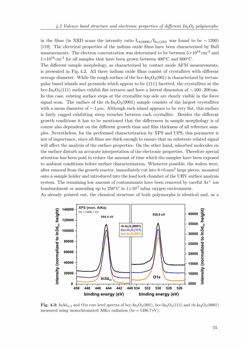
4.2 Valence band structure and electronic properties of different In2O3 polymorphs
in the films (in XRD scans the intensity ratio Irh(0006)/Ibcc(222) was found to be ∼ 1200)[119]. The electrical properties of the indium oxide films have been characterized by Hallmeasurements. The electron concentration was determined to be between 5×1018 cm-3 and1×1019 cm-3 for all samples that have been grown between 400C and 600C.The different sample morphology, as characterized by contact mode AFM measurements,is presented in Fig. 4.2. All three indium oxide films consist of crystallites with differentaverage diameter. While the rough surface of the bcc-In2O3(001) is characterized by rectan-gular based islands and pyramids which appear to be 111 facetted, the crystallites at thebcc-In2O3(111) surface exhibit flat terraces and have a lateral dimension of ∼ 100 - 200 nm.In this case, existing surface steps at the crystallite top side are clearly visible in the forcesignal scan. The surface of the rh-In2O3(0001) sample consists of the largest crystalliteswith a mean diameter of ∼ 1 µm. Although each island appears to be very flat, this surfaceis fairly ragged exhibiting steep trenches between each crystallite. Besides the differentgrowth conditions it has to be mentioned that the differences in sample morphology is ofcourse also dependent on the different growth time and film thickness of all reference sam-ples. Nevertheless, for the performed characterization by XPS and UPS, this parameter isnot of importance, since all films are thick enough to ensure that no substrate related signalwill affect the analysis of the surface properties. On the other hand, adsorbed molecules onthe surface disturb an accurate interpretation of the electronic properties. Therefore specialattention has been paid to reduce the amount of time which the samples have been exposedto ambient conditions before surface characterization. Whenever possible, the wafers were,after removal from the growth reactor, immediately cut into 8×6 mm2 large pieces, mountedonto a sample holder and introduced into the load lock chamber of the UHV surface analysissystem. The remaining low amount of contaminants have been removed by careful Ar+ ionbombardment or annealing up to 250C in 1×10⁻⁷ mbar oxygen environment.As already pointed out, the chemical structure of both polymorphs is identical and, as a
4404424444464484500
20000
40000
60000
80000
100000
120000
140000
534 532 530 528 526
5000
10000
15000
20000
25000
30000
35000
40000
binding energy (eV) binding energy (eV)
inte
ns
ity
(n
orm
alize
d t
o In
3d
he
igh
t)5/2
inte
ns
ity
(n
orm
alize
d t
o In
3d
he
igh
t)5/2
XPS (mon. AlK )hν = 1486.7 eV
á
In3d5/2O1s
530.0 eV444.4 eV
rh-In O (0001)2 3
bcc-In O (111)2 3
bcc-In O (001)2 3
Fig. 4.3: In3d5/2 and O1s core level spectra of bcc-In2O3(001), bcc-In2O3(111) and rh-In2O3(0001)measured using monochromated AlKα radiation (hν =1486.7 eV).
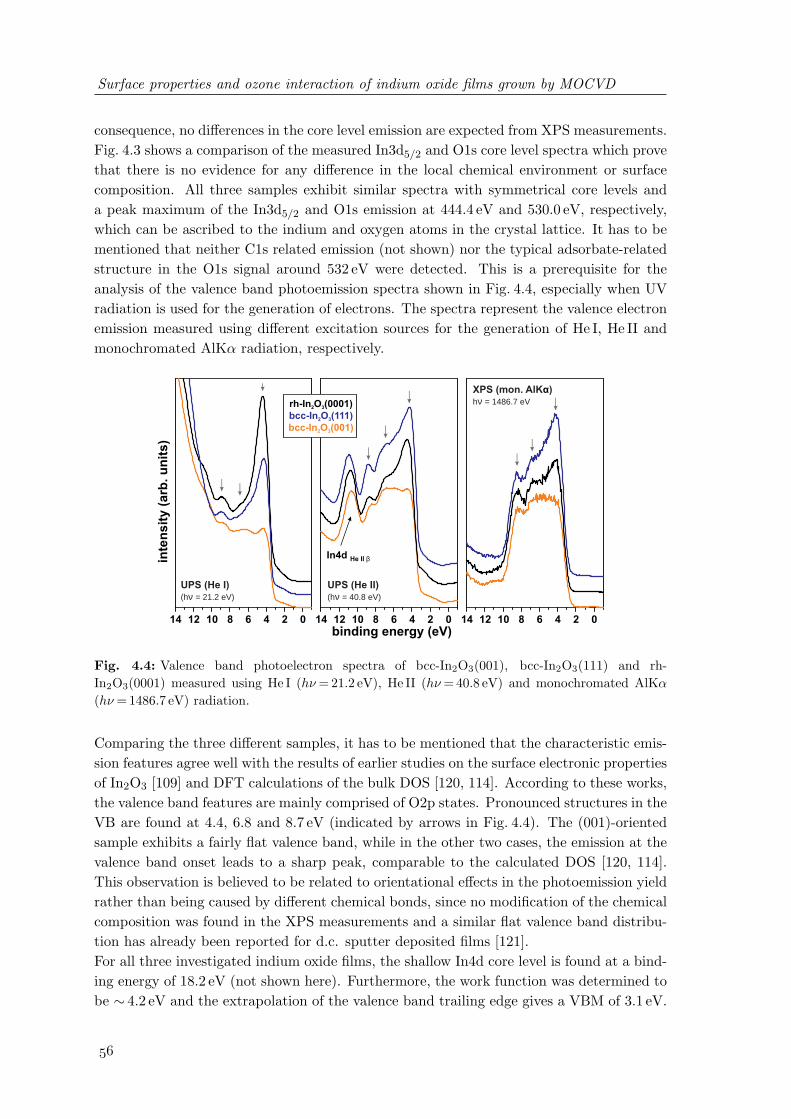
Surface properties and ozone interaction of indium oxide films grown by MOCVD
consequence, no differences in the core level emission are expected from XPS measurements.Fig. 4.3 shows a comparison of the measured In3d5/2 and O1s core level spectra which provethat there is no evidence for any difference in the local chemical environment or surfacecomposition. All three samples exhibit similar spectra with symmetrical core levels anda peak maximum of the In3d5/2 and O1s emission at 444.4 eV and 530.0 eV, respectively,which can be ascribed to the indium and oxygen atoms in the crystal lattice. It has to bementioned that neither C1s related emission (not shown) nor the typical adsorbate-relatedstructure in the O1s signal around 532 eV were detected. This is a prerequisite for theanalysis of the valence band photoemission spectra shown in Fig. 4.4, especially when UVradiation is used for the generation of electrons. The spectra represent the valence electronemission measured using different excitation sources for the generation of He I, He II andmonochromated AlKα radiation, respectively.
14 12 10 8 6 4 2 0
in
ten
sit
y (
arb
. u
nit
s)
binding energy (eV)02468101214 14 12 10 8 6 4 2 0
rh-In O (0001)2 3
bcc-In O (111)2 3
bcc-In O (001)2 3
XPS (mon. AlK )hν = 1486.7 eV
á
UPS (He II)(hν = 40.8 eV)
UPS (He I)(hν = 21.2 eV)
In4d He II β
Fig. 4.4: Valence band photoelectron spectra of bcc-In2O3(001), bcc-In2O3(111) and rh-In2O3(0001) measured using He I (hν =21.2 eV), He II (hν =40.8 eV) and monochromated AlKα
(hν =1486.7 eV) radiation.
Comparing the three different samples, it has to be mentioned that the characteristic emis-sion features agree well with the results of earlier studies on the surface electronic propertiesof In2O3 [109] and DFT calculations of the bulk DOS [120, 114]. According to these works,the valence band features are mainly comprised of O2p states. Pronounced structures in theVB are found at 4.4, 6.8 and 8.7 eV (indicated by arrows in Fig. 4.4). The (001)-orientedsample exhibits a fairly flat valence band, while in the other two cases, the emission at thevalence band onset leads to a sharp peak, comparable to the calculated DOS [120, 114].This observation is believed to be related to orientational effects in the photoemission yieldrather than being caused by different chemical bonds, since no modification of the chemicalcomposition was found in the XPS measurements and a similar flat valence band distribu-tion has already been reported for d.c. sputter deposited films [121].For all three investigated indium oxide films, the shallow In4d core level is found at a bind-ing energy of 18.2 eV (not shown here). Furthermore, the work function was determined tobe ∼ 4.2 eV and the extrapolation of the valence band trailing edge gives a VBM of 3.1 eV.

4.2 Valence band structure and electronic properties of different In2O3 polymorphs
The energetic position of the valence band maximum with respect to the Fermi level has alsobeen reported in earlier works to lie around 3 eV [109, 122]. As already explained for theInN measurements, the measured value EF - VBM is mainly determined by two parameters:i) the energetic position of the bulk Fermi level and ii) the band bending at the surface.Since In2O3 is a degenerate semiconductor, the Fermi level is located inside the conductionband and the occupation of the conduction states is dependent on the carrier concentrationinside the film. According to recent band structure calculations, for an electron concen-tration in the range between 5×1018 cm-3 and 1×1019 cm-3, which is present in the filmsinvestigated here, the bulk Fermi level is located ∼ 50 - 70meV above the conduction bandminimum [114]. Under the assumption of a band gap of 3.6 eV, photoelectron spectroscopyindicates a strong upward band bending, as discussed in [123]. However, this model doesnot agree very well with the observed variation of the conductivity of these films uponoxidation and reduction of indium oxide sensor surfaces. This discrepancy led, for exam-ple, to the proposal of a modified band gap at reduced In2O3 surfaces [111]. The recentlydiscussed lower band gap value of 2.9 - 3.1 eV would describe the electrical characteristicsof the films much better. The band alignment at the In2O3 surface for these three differentband gap values is schematically plotted in Fig. 4.5. In contrast to the strong upward bandbending in the case of Eg = 3.6 eV, for the experimentally determined distance between EF
and the surface VBM, almost flat band conditions would result for a band gap around 3 eV.Depending on the exact value, slight upward or downward band bending of about 100 meVwould result. A final picture cannot be developed for the band alignment at the In2O3
surface at the moment since too many uncertainties are still existing in the experimentalresults as well as in the theoretical calculations. Nevertheless, a scenario with almost flatband conditions is more favorable.
CBM
EF
VBM
(E-V
BM
)=
3.1
eV
F
(E -CBM) ~ 50 meVF
3.6 eV3.1 eV 2.9 eV
Fig. 4.5: Model of the band alignment at In2O3 surface depending on different band gap energiesof 3.6, 3.1 or 2.9 eV. The left scenario corresponds to the common picture of strong upward bandbending [123], while in the case that the real band gap is around 3 eV [114, 117], an almost flatband distribution would result.
The characteristics of the three different stoichiometric and crystalline indium oxide samplespresented above are the reference for a subsequent analysis of the surface properties ofnanocrystalline In2O3−x films prepared by MOCVD at very low temperatures discussedin the next section. As will be shown below, the high sensitivity of these films towardsozone is related to differences in the indium oxide crystallite size as well as in the surfacecomposition of the material.

Surface properties and ozone interaction of indium oxide films grown by MOCVD
4.3 Non-stoichiometry and defect states in In2O3 films grown
by MOCVD at low temperatures
Upon a detailed study of the ozone sensing characteristics of polycrystalline indium oxidethin films prepared by MOCVD, it was established that the ozone detection efficiency isstrongly dependent on the growth temperature used. For films prepared at temperatures aslow as 200C, a sensitivity of up to 105 was observed for an ozone concentration of ∼ 10 ppmand a remarkably low response time of ∼ 1 s could be achieved for 10 nm thick films. Byimplementing these films into sensor devices, it was possible to reduce the detection limitto around 15 ppb O3 [100]. The ozone sensitivity dependence of the indium oxide films ismainly caused by two reasons. First, there is a strong relation between the indium oxideparticle size and the used deposition temperature. As demonstrated in Fig. 4.2, for growthtemperatures above 400C, the crystallites have an average diameter of a few hundred nm.Upon reducing the growth temperature, the particle size is strongly decreased, approachinga value of 7 - 8 nm around 200C. The typical crystal structure of such an indium oxide filmgrown at 200C (this type of sample is subsequently denoted “LT-InOx”) is presented inFig. 4.6. On the left side, a transmission electron micrograph of a LT-InOx/Al2O3 interfaceis shown, indicating the existence of a closed film of single crystallites with a diameter of
2x2 2 µm z-scale: 7.5 nN z-sale: 1.1 nN F-scale: 5.6 nN
z-scale: 250 nm z-sale: 8.2 nm z-scale: 16.5 nm2x2 2 µm
2x1 1 µm
2x1 1 µm
2x1 1 µm
2x1 1 µm
30 nm
Fig. 4.6: Crystal structure and surface topography of nanocrystalline indium oxide grown byMOCVD at 200C. Left picture: TEM (transmission electron microscopy) image and SAED (se-lected area electron diffraction) pattern (inset) of the nanoparticles [100]. The small grain size isalso observed in contact AFM measurements (picture on the right).

4.3 Non-stoichiometry and defect states in In2O3 films grown by MOCVD at lowtemperatures
less than 10 nm [100]. On the right side of the figure, corresponding atomic force micro-graphs are presented. Due to the low substrate temperature, the chemical reactions areinhibited, the adsorption/desorption ratio of molecules of the gas phase is strongly modifiedand especially the low diffusion rate of atoms and molecules at the surface of the formednuclei leads to the formation of only small particles, while the resulting grain size at highertemperatures is much larger. The porous nanocrystalline character of these LT-InOx filmsis clearly visible and is one reason for the observed high ozone sensitivity. It is stronglyenhanced by the fact that the active surface, where the reaction with ozone takes place,is strongly increased. However, as will be discussed in the following, the nanocrystallinestructure of these LT-InOx films is not the only difference compared to conventional In2O3
films.The surface stoichiometry of these films was characterized by X-ray photoelectron spec-troscopy measurements. Differences in the chemical composition can be deduced from thecomparison of results from LT-InOx samples with the measurements of conventional In2O3
films as presented in Figs. 4.7 and 4.8. All electron states shift by 0.2 eV towards higher
4404454504554604650
10000
20000
30000
40000
50000
60000
70000
80000
5265285305325344000
6000
8000
10000
12000
14000
16000
18000
20000
22000
24000
14.3 eV
18.8 eV
plasmon losses
binding energy (eV) binding energy (eV)
inte
ns
ity
(n
orm
alize
d t
o In
3d
he
igh
t)5
/2
inte
ns
ity
(n
orm
alize
d t
o In
3d
he
igh
t)5
/2
XPS (mon. AlK )hν = 1486.7 eV
á
In3d
O1s
In O2 3
LT-InOx
530.0 eV
44
4.4
eV
0.2 eV
530.2 eV
444.6 eV
Fig. 4.7: Comparison of the In3d and O1s core level spectra between crystalline In2O3 grown above400C and nanocrystalline LT-InOx deposited at 200C.
binding energy. An explanation for this observation will be discussed below together withthe changes in the valence band emission. The most prominent difference of LT-InOx is thedrastically reduced amount of oxygen at the surface compared to stoichiometric In2O3 filmsgrown at higher temperatures. From analysis of the peak area ratio of the single electroncore level contributions it was determined that the oxygen content is reduced to ∼ 67%,which corresponds to a 1:1 proportion of indium and oxygen at the surface. Therefore,it can be concluded that the very low deposition temperature leads to a highly oxygen-deficient and sub-stoichiometric material.A similar result has been found for nanocrystalline indium oxide prepared by spray pyrol-
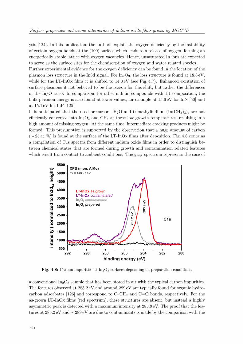
Surface properties and ozone interaction of indium oxide films grown by MOCVD
ysis [124]. In this publication, the authors explain the oxygen deficiency by the instabilityof certain oxygen bonds at the (100) surface which leads to a release of oxygen, forming anenergetically stable lattice with oxygen vacancies. Hence, unsaturated In ions are expectedto serve as the surface sites for the chemisorption of oxygen and water related species.Further experimental evidence for the oxygen deficiency can be found in the location of theplasmon loss structure in the In3d signal. For In2O3, the loss structure is found at 18.8 eV,while for the LT-InOx films it is shifted to 14.3 eV (see Fig. 4.7). Enhanced excitation ofsurface plasmons it not believed to be the reason for this shift, but rather the differencesin the In/O ratio. In comparison, for other indium compounds with 1:1 composition, thebulk plasmon energy is also found at lower values, for example at 15.6 eV for InN [50] andat 15.1 eV for InP [125].It is anticipated that the used precursors, H2O and trimethylindium (In(CH3)3), are notefficiently converted into In2O3 and CH4 at these low growth temperatures, resulting in ahigh amount of missing oxygen. At the same time, intermediate cracking products might beformed. This presumption is supported by the observation that a huge amount of carbon(∼ 25 at.%) is found at the surface of the LT-InOx films after deposition. Fig. 4.8 containsa compilation of C1s spectra from different indium oxide films in order to distinguish be-tween chemical states that are formed during growth and contamination related featureswhich result from contact to ambient conditions. The gray spectrum represents the case of
292 290 288 286 284 282 280500
1000
1500
2000
2500
3000
3500
4000
4500
5000
5500
inte
ns
ity
(n
orm
alize
d t
o In
3d
he
igh
t)5/2
XPS (mon. AlK )hν = 1486.7 eV
á
C1s
28
3.9
eV
LT-InOx as grown
In O prepared2 3
LT-InOx contaminatedIn O contaminated2 3
28
5.2
eV
binding energy (eV)
Fig. 4.8: Carbon impurities at In2O3 surfaces depending on preparation conditions.
a conventional In2O3 sample that has been stored in air with the typical carbon impurities.The features observed at 285.2 eV and around 289 eV are typically found for organic hydro-carbon adsorbates [126] and correspond to C–CHx and C=O bonds, respectively. For theas-grown LT-InOx films (red spectrum), these structures are absent, but instead a highlyasymmetric peak is detected with a maximum intensity at 283.9 eV. The proof that the fea-tures at 285.2 eV and ∼ 289 eV are due to contaminants is made by the comparison with the
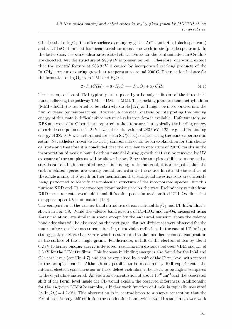
4.3 Non-stoichiometry and defect states in In2O3 films grown by MOCVD at lowtemperatures
C1s signal of a In2O3 film after surface cleaning by gentle Ar+ sputtering (black spectrum)and a LT-InOx film that has been stored for about one week in air (purple spectrum). Inthe latter case, the same adsorbate-related structures as for the contaminated In2O3 filmsare detected, but the structure at 283.9 eV is present as well. Therefore, one would expectthat the spectral feature at 283.9 eV is caused by incorporated cracking products of theIn(CH3)3 precursor during growth at temperatures around 200C. The reaction balance forthe formation of In2O3 from TMI and H2O is
2 · In(CH3)3 + 3 ·H2O −→ In2O3 + 6 · CH4 (4.1)
The decomposition of TMI typically takes place by a homolytic fission of the three In-Cbonds following the pathway TMI→DMI→MMI. The cracking product monomethylindium(MMI - InCH3) is reported to be relatively stable [127] and might be incorporated into thefilm at these low temperatures. However, a chemical analysis by interpreting the bindingenergy of this state is difficult since not much reference data is available. Unfortunately, noXPS analyses of In–C bonds are reported in the literature, but typically the binding energyof carbide compounds is 1 - 2 eV lower than the value of 283.9 eV [128], e.g. a C1s bindingenergy of 282.9 eV was determined for clean SiC(0001) surfaces using the same experimentalsetup. Nevertheless, possible In-CxHy components could be an explanation for this chemi-cal state and therefore it is concluded that the very low temperature of 200C results in theincorporation of weakly bound carbon material during growth that can be removed by UVexposure of the samples as will be shown below. Since the samples exhibit so many activesites because a high amount of oxygen is missing in the material, it is anticipated that thecarbon related species are weakly bound and saturate the active In sites at the surface ofthe single grains. It is worth further mentioning that additional investigations are currentlybeing performed to identify the molecular structure of the incorporated species. For thispurpose XRD and IR-spectroscopy examinations are on the way. Preliminary results fromXRD measurements reveal additional diffraction peaks for as-deposited LT-InOx films thatdisappear upon UV illumination [129].The comparison of the valence band structures of conventional In2O3 and LT-InOx films isshown in Fig. 4.9. While the valence band spectra of LT-InOx and In2O3, measured usingX-ray radiation, are similar in shape except for the enhanced emission above the valenceband edge that will be discussed on the next page, distinct differences were observed for themore surface sensitive measurements using ultra-violet radiation. In the case of LT-InOx, astrong peak is detected at ∼ 9 eV which is attributed to the modified chemical compositionat the surface of these single grains. Furthermore, a shift of the electron states by about0.2 eV to higher binding energy is detected, resulting in a distance between VBM and EF of3.3 eV for the LT-InOx films. This increase in binding energy is also found for the In3d andO1s core levels (see Fig. 4.7) and can be explained by a shift of the Fermi level with respectto the occupied bands. Although not possible to be measured by Hall experiments, theinternal electron concentration in these defect-rich films is believed to be higher comparedto the crystalline material. An electron concentration of about 1020 cm-3 and the associatedshift of the Fermi level inside the CB would explain the observed differences. Additionally,for the as-grown LT-InOx samples, a higher work function of 4.4 eV is typically measured(φ (In2O3) = 4.2 eV). This observation is in contradiction to a simple conception that theFermi level is only shifted inside the conduction band, which would result in a lower work
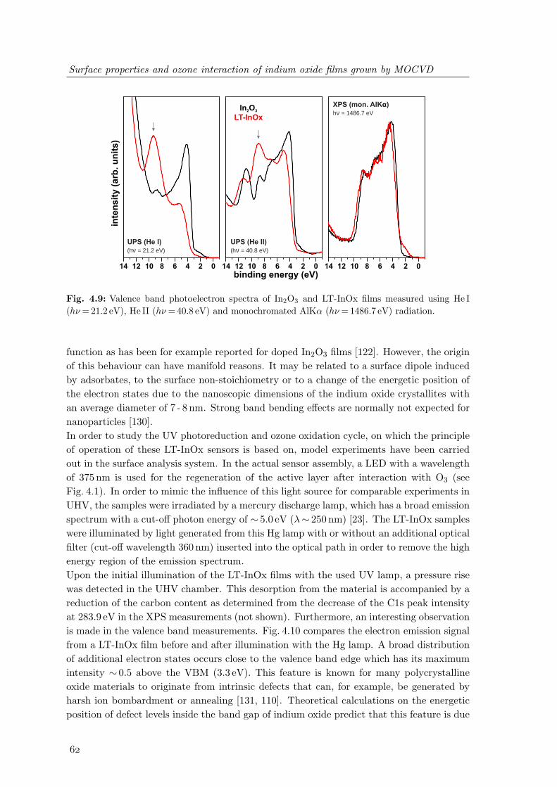
Surface properties and ozone interaction of indium oxide films grown by MOCVD
14 12 10 8 6 4 2 0 14 12 10 8 6 4 2 0 14 12 10 8 6 4 2 0
in
ten
sit
y (
arb
. u
nit
s)
binding energy (eV)
In O2 3
LT-InOx
XPS (mon. AlK )hν = 1486.7 eV
á
UPS (He II)(hν = 40.8 eV)
UPS (He I)(hν = 21.2 eV)
Fig. 4.9: Valence band photoelectron spectra of In2O3 and LT-InOx films measured using He I(hν =21.2 eV), He II (hν =40.8 eV) and monochromated AlKα (hν =1486.7 eV) radiation.
function as has been for example reported for doped In2O3 films [122]. However, the originof this behaviour can have manifold reasons. It may be related to a surface dipole inducedby adsorbates, to the surface non-stoichiometry or to a change of the energetic position ofthe electron states due to the nanoscopic dimensions of the indium oxide crystallites withan average diameter of 7 - 8 nm. Strong band bending effects are normally not expected fornanoparticles [130].In order to study the UV photoreduction and ozone oxidation cycle, on which the principleof operation of these LT-InOx sensors is based on, model experiments have been carriedout in the surface analysis system. In the actual sensor assembly, a LED with a wavelengthof 375 nm is used for the regeneration of the active layer after interaction with O3 (seeFig. 4.1). In order to mimic the influence of this light source for comparable experiments inUHV, the samples were irradiated by a mercury discharge lamp, which has a broad emissionspectrum with a cut-off photon energy of ∼ 5.0 eV (λ∼ 250 nm) [23]. The LT-InOx sampleswere illuminated by light generated from this Hg lamp with or without an additional opticalfilter (cut-off wavelength 360 nm) inserted into the optical path in order to remove the highenergy region of the emission spectrum.Upon the initial illumination of the LT-InOx films with the used UV lamp, a pressure risewas detected in the UHV chamber. This desorption from the material is accompanied by areduction of the carbon content as determined from the decrease of the C1s peak intensityat 283.9 eV in the XPS measurements (not shown). Furthermore, an interesting observationis made in the valence band measurements. Fig. 4.10 compares the electron emission signalfrom a LT-InOx film before and after illumination with the Hg lamp. A broad distributionof additional electron states occurs close to the valence band edge which has its maximumintensity ∼ 0.5 above the VBM (3.3 eV). This feature is known for many polycrystallineoxide materials to originate from intrinsic defects that can, for example, be generated byharsh ion bombardment or annealing [131, 110]. Theoretical calculations on the energeticposition of defect levels inside the band gap of indium oxide predict that this feature is due
4.3 Non-stoichiometry and defect states in In2O3 films grown by MOCVD at lowtemperatures
EF
VB
3.3
eV
0.5 eV
6 5 4 3 2 1 0 -1
inte
ns
ity
(a
rb. u
nit
s)
binding energy (eV)
defectstates
LT-InOx + Hg lampLT-InOx untreated
XPS (mon. AlK )hν = 1486.7 eV
á
nanoparticle oxygen deficient layer
Fig. 4.10: UV-induced changes of the valence band states of LT-InOx films. Defects states aregenerated approximately 0.5 eV above the valence band maximum. The schematic depicts theproposed formation of a strongly reduced crystallite surface layer with a high content of oxygenvacancies.
to the existence of oxygen vacancies [132, 133], which is conform to the properties of otherunstoichiometric oxide surfaces, such as SnO2−x and TiO2−x. Therefore, the observationof the defect states above the VBM in the PES spectra can be used as indicator for theexistence of oxygen defects, or more correctly In derived states (5s-5p) arising from brokenIn-O bonds [111]. For each missing oxygen atom, up to two additional electrons are existingin the material which are contributing to a higher electron concentration. In consequence,the remaining unsaturated indium ions are very reactive and can act as centers for theadsorption of atoms and molecules. Nevertheless, the large amount of these defect statesfor the LT-InOx films after UV irradiation is surprising and points towards a high concen-tration of reactive centers at the surface of the 7 - 8 nm large indium oxide crystallites.
Summarizing the results from the structural and spectroscopic characterization of indiumoxide films grown by MOCVD at 200C, the following conclusions can be drawn: Due tothe low growth temperature and hence limited diffusion of adatoms at nuclei, the crystallitediameter is in the range of a few nanometer. These nanocrystals exhibit a strong deviationin the surface stoichiometry compared to conventional In2O3 films. A reduction of the oxy-gen content of - 33% was observed. It is anticipated that especially the outermost layers ofthe particles consist of a high degree of oxygen vacancies resulting in the existence of excesselectrons, which are partially localized at the remaining indium atoms forming reactive de-fect sites. The proposed scenario is schematically depicted at the right bottom of Fig. 4.10.The existence of an oxygen deficient top layer results in a very high reaction potential ofthe nanocrystal surface. During growth in the reaction chamber, the defects are decoratedwith cracking products from the used In(CH3)3 that are weakly bound to the surface of
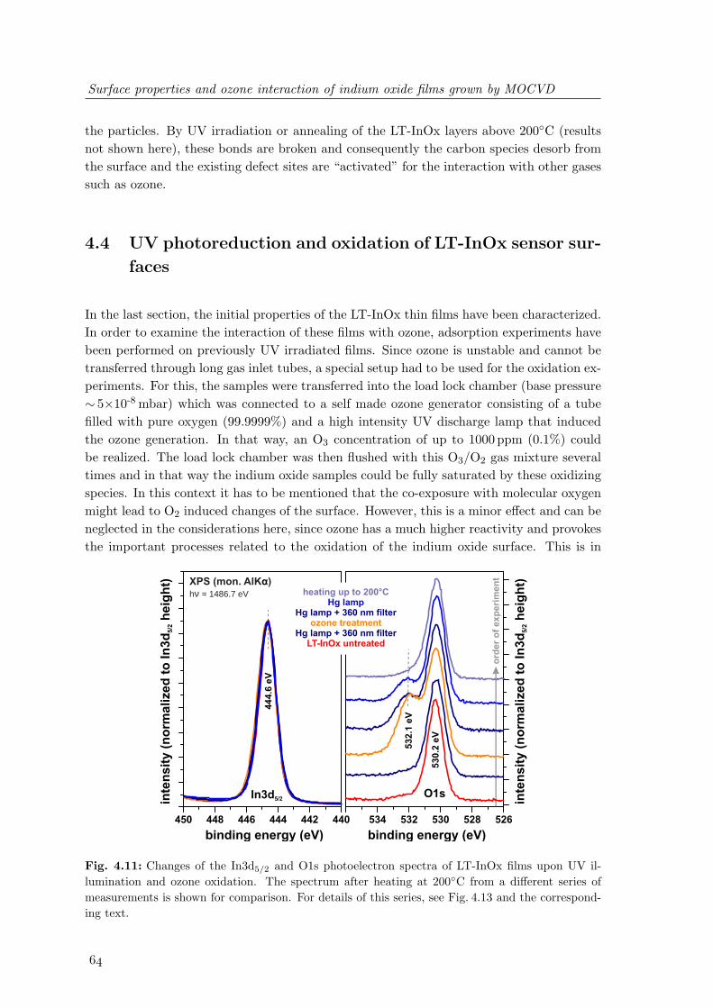
Surface properties and ozone interaction of indium oxide films grown by MOCVD
the particles. By UV irradiation or annealing of the LT-InOx layers above 200C (resultsnot shown here), these bonds are broken and consequently the carbon species desorb fromthe surface and the existing defect sites are “activated” for the interaction with other gasessuch as ozone.
4.4 UV photoreduction and oxidation of LT-InOx sensor sur-
faces
In the last section, the initial properties of the LT-InOx thin films have been characterized.In order to examine the interaction of these films with ozone, adsorption experiments havebeen performed on previously UV irradiated films. Since ozone is unstable and cannot betransferred through long gas inlet tubes, a special setup had to be used for the oxidation ex-periments. For this, the samples were transferred into the load lock chamber (base pressure∼ 5×10⁻⁸ mbar) which was connected to a self made ozone generator consisting of a tubefilled with pure oxygen (99.9999%) and a high intensity UV discharge lamp that inducedthe ozone generation. In that way, an O3 concentration of up to 1000 ppm (0.1%) couldbe realized. The load lock chamber was then flushed with this O3/O2 gas mixture severaltimes and in that way the indium oxide samples could be fully saturated by these oxidizingspecies. In this context it has to be mentioned that the co-exposure with molecular oxygenmight lead to O2 induced changes of the surface. However, this is a minor effect and can beneglected in the considerations here, since ozone has a much higher reactivity and provokesthe important processes related to the oxidation of the indium oxide surface. This is in
440442444446448450 526528530532534
binding energy (eV) binding energy (eV)
inte
ns
ity
(n
orm
alize
d t
o In
3d
he
igh
t)5/2
inte
ns
ity
(n
orm
alize
d t
o In
3d
he
igh
t)5/2
XPS (mon. AlK )hν = 1486.7 eV
á
In3d5/2O1s
44
4.6
eV
53
2.1
eV
53
0.2
eV
ord
er
of
ex
pe
rim
en
t
heating up to 200°CHg lamp
Hg lamp + 360 nm filter
Hg lamp + 360 nm filterozone treatment
LT-InOx untreated
Fig. 4.11: Changes of the In3d5/2 and O1s photoelectron spectra of LT-InOx films upon UV il-lumination and ozone oxidation. The spectrum after heating at 200C from a different series ofmeasurements is shown for comparison. For details of this series, see Fig. 4.13 and the correspond-ing text.

4.4 UV photoreduction and oxidation of LT-InOx sensor surfaces
agreement with the electrical characterization, where only a minor influence of the sensorperformance on the co-existence of O2 is found. The interaction of the LT-InOx films withO2 and further oxygen containing molecules is examined in more detail at the end of thissection.Figs. 4.11 and 4.12 represent photoelectron spectra measured during a cycle of successiveUV-irradiation and ozone oxidation treatments of a LT-InOx sample. As already discussed,the initial UV exposure has only influence on the C1s signal, which is reduced in combina-tion with the formation of the oxygen vacancy related states above the VBM. When thesamples are brought into contact with ozone, distinct spectral signatures are observed. Firstof all, an additional component in the O1s signal is detected at 532.1 eV. It has approx-imately 50% of the intensity of the initial oxygen signal, which corresponds to a captureof the initially missing ∼ 33% of oxygen. Therefore, it can be stated that the interac-tion with O3 is very efficient to compensate the oxygen deficiency inside the material sincemany of the active sites are decorated by the provided adsorbates. However, the oxygenis not incorporated into the crystal structure forming In2O3, since the chemical bonds ofthe additional oxygen have a different binding energy. The occurrence of the feature at532.1 eV is similar to observation reported in earlier works on the interaction of ozone withindium oxide films prepared by sol-gel methods [97, 102]. The difference between the filmsprepared by sol-gel compared to the MOCVD films is that they initially already exhibit alarge amount of oxygen adsorbates before ozone interaction.In addition to the In3d and O1s core level measurements, examinations of the valence bandstructure upon O3 interaction gives further information on the adsorption process. Theemission from the defect states, which is not as pronounced in the UPS measurements com-pared to the results from XPS (for comparison see the respective spectra after illuminationwith the Hg lamp without filter in Fig. 4.10 and Fig. 4.12), is strongly reduced. Further-
02468101214 024681012
11.3 eV6.2 eV
binding energy (eV) binding energy (eV)
ozone treatment
ozone treatment
Hg lampHg lamp + 360 nm filter
Hg lamp + 360 nm filterLT-InOx untreated
UPS (He II)hν = 40.8 eV
UPS (He I)hν = 21.2 eV
inte
ns
ity
(a
rb. u
nit
s)
5.1 eV
ord
er
of
ex
pe
rim
en
t
Fig. 4.12: Changes of the valence states of LT-InOx films upon ozone oxidation and subsequentUV illumination.

Surface properties and ozone interaction of indium oxide films grown by MOCVD
more, two features due to oxygen adsorbate related states appear in the valence band at6.2 and 11.3 eV and the valence band maximum is shifted by 0.2 eV away from EF .The regeneration of the sensor is implemented by illumination with UV light. PES experi-ments on the influence of the UV irradiation after ozone oxidation show that the adsorbatesare partially desorbed, but do not completely recover the initial conditions as after growth.As can be deduced from Figs. 4.11 and 4.12, the emission from the structures associated tothe oxygen adsorbates are only in parts reduced to about 50%. The degree of desorptionis further dependent on the used light intensity and, more critically, the wavelength. Forthe measurements performed after illumination with the Hg lamp without filter, the high-est degree of adsorbate removal is achieved. In this case, the reappearance of the defectsstates in the photoelectron spectra is also stronger and the valence band edge shifts backto the initial value of 3.3 eV. Upon the second cycle of oxidation, the same properties arefound as after the first cycle. Hence, once the sensor is initiated by UV irradiation, theLT-InOx films can be reversibly oxidized and reduced by ozone oxidation and subsequentUV illumination. Thus, while the initial surface configuration after deposition might notbe recoverable, the surface stoichiometry is altered within steady state conditions.Since the ozone sensors can also be reactivated by annealing, the desorption of oxygenadsorbates upon thermal treatment were additionally investigated. Measurements of thevalence band and In4d level during gradual increase of substrate temperature of an ozoneoxidized LT-InOx film are presented in Fig. 4.13. Initially the surface exhibits the adsor-
20 19 18 17 16 14 12 10 8 6 4 2 0binding energy (eV)
200°C
RTinte
ns
ity
(a
rb. u
nit
s)
defects
an
ne
alin
g
UPS (He II)hν = 40.8 eV
In4d
150°C
LT-InOx after ozone treatment
Fig. 4.13: Temperature dependent desorption of ozone-induced adsorbates from LT-InOx surfaces.
bate related spectral features at 6.2 and 11.3 eV. A reduction of this emission is detected attemperatures above 150C and the defect states induced emission above the VBM increasessimultaneously with oxygen desorption. Finally the adsorbates are completely removed attemperatures above 200C and the valence band spectrum becomes similar to LT-InOx.Additionally a shift of the valence states by ∼ 0.2 eV is detected (best visible in the shift ofthe In4d peak maximum). In contrast to the regeneration of the surface with UV light, for
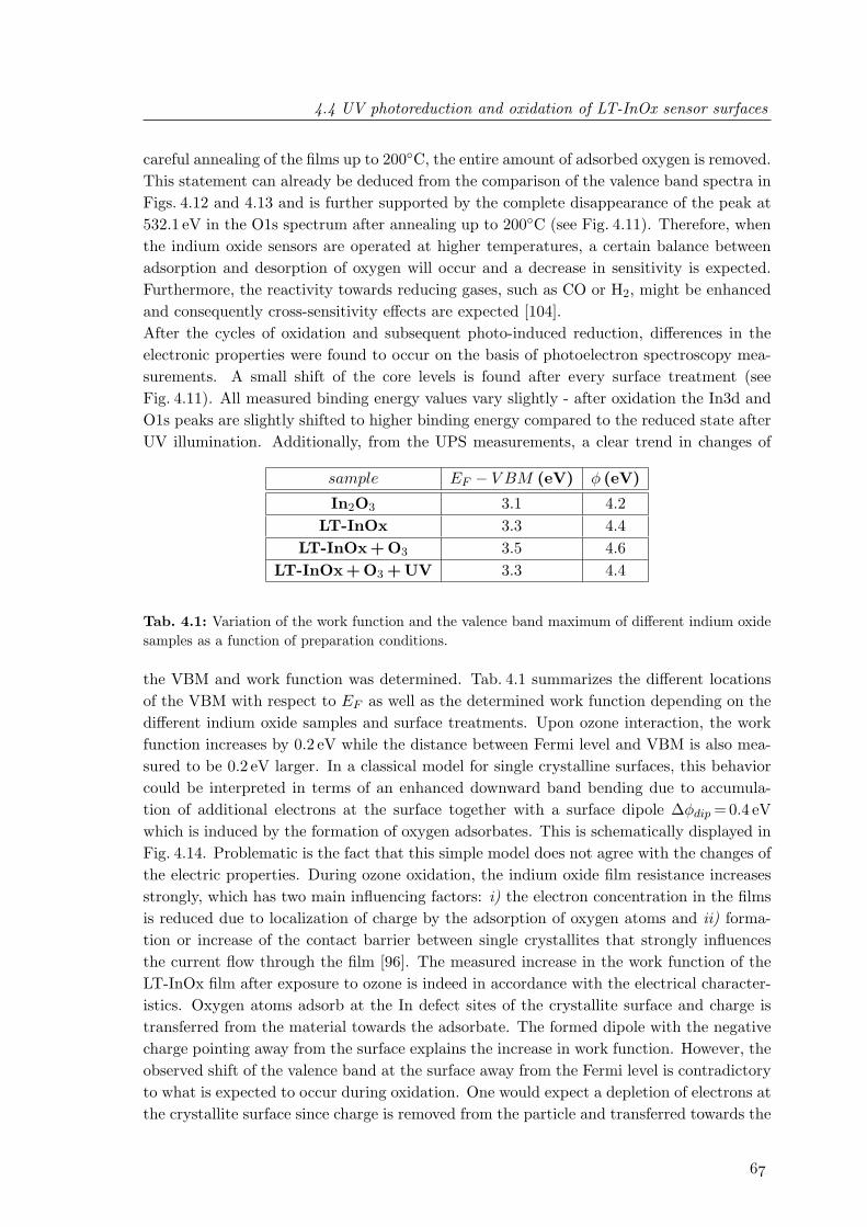
4.4 UV photoreduction and oxidation of LT-InOx sensor surfaces
careful annealing of the films up to 200C, the entire amount of adsorbed oxygen is removed.This statement can already be deduced from the comparison of the valence band spectra inFigs. 4.12 and 4.13 and is further supported by the complete disappearance of the peak at532.1 eV in the O1s spectrum after annealing up to 200C (see Fig. 4.11). Therefore, whenthe indium oxide sensors are operated at higher temperatures, a certain balance betweenadsorption and desorption of oxygen will occur and a decrease in sensitivity is expected.Furthermore, the reactivity towards reducing gases, such as CO or H2, might be enhancedand consequently cross-sensitivity effects are expected [104].After the cycles of oxidation and subsequent photo-induced reduction, differences in theelectronic properties were found to occur on the basis of photoelectron spectroscopy mea-surements. A small shift of the core levels is found after every surface treatment (seeFig. 4.11). All measured binding energy values vary slightly - after oxidation the In3d andO1s peaks are slightly shifted to higher binding energy compared to the reduced state afterUV illumination. Additionally, from the UPS measurements, a clear trend in changes of
sample EF − V BM (eV) φ (eV)
In2O3 3.1 4.2LT-InOx 3.3 4.4
LT-InOx + O3 3.5 4.6LT-InOx + O3 + UV 3.3 4.4
Tab. 4.1: Variation of the work function and the valence band maximum of different indium oxidesamples as a function of preparation conditions.
the VBM and work function was determined. Tab. 4.1 summarizes the different locationsof the VBM with respect to EF as well as the determined work function depending on thedifferent indium oxide samples and surface treatments. Upon ozone interaction, the workfunction increases by 0.2 eV while the distance between Fermi level and VBM is also mea-sured to be 0.2 eV larger. In a classical model for single crystalline surfaces, this behaviorcould be interpreted in terms of an enhanced downward band bending due to accumula-tion of additional electrons at the surface together with a surface dipole ∆φdip =0.4 eVwhich is induced by the formation of oxygen adsorbates. This is schematically displayed inFig. 4.14. Problematic is the fact that this simple model does not agree with the changes ofthe electric properties. During ozone oxidation, the indium oxide film resistance increasesstrongly, which has two main influencing factors: i) the electron concentration in the filmsis reduced due to localization of charge by the adsorption of oxygen atoms and ii) forma-tion or increase of the contact barrier between single crystallites that strongly influencesthe current flow through the film [96]. The measured increase in the work function of theLT-InOx film after exposure to ozone is indeed in accordance with the electrical character-istics. Oxygen atoms adsorb at the In defect sites of the crystallite surface and charge istransferred from the material towards the adsorbate. The formed dipole with the negativecharge pointing away from the surface explains the increase in work function. However, theobserved shift of the valence band at the surface away from the Fermi level is contradictoryto what is expected to occur during oxidation. One would expect a depletion of electrons atthe crystallite surface since charge is removed from the particle and transferred towards the
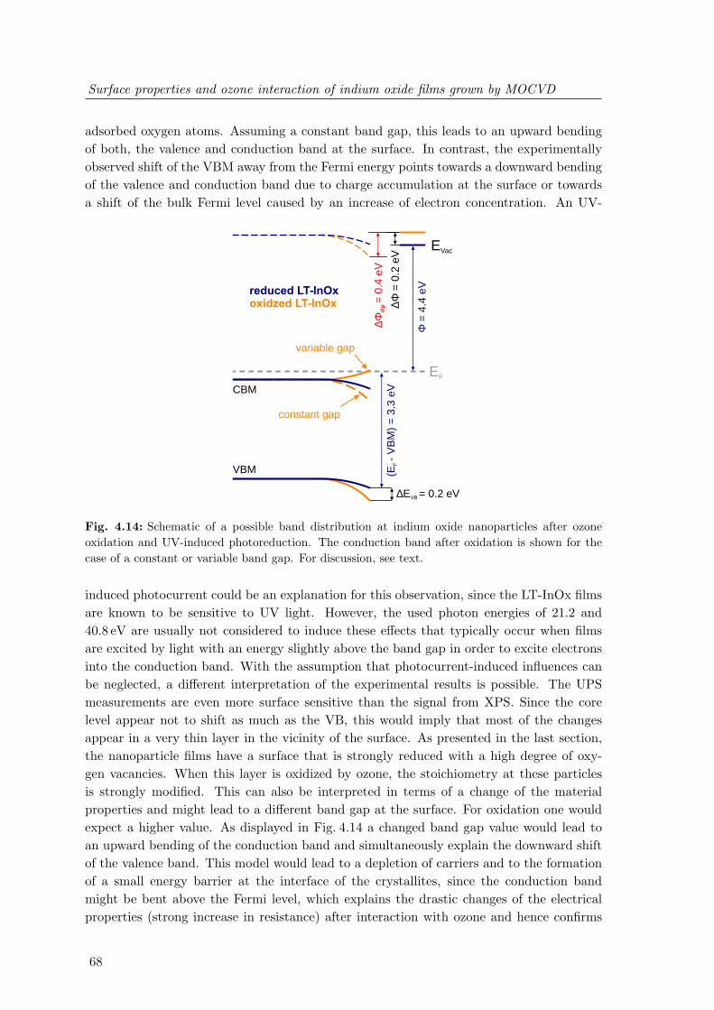
Surface properties and ozone interaction of indium oxide films grown by MOCVD
adsorbed oxygen atoms. Assuming a constant band gap, this leads to an upward bendingof both, the valence and conduction band at the surface. In contrast, the experimentallyobserved shift of the VBM away from the Fermi energy points towards a downward bendingof the valence and conduction band due to charge accumulation at the surface or towardsa shift of the bulk Fermi level caused by an increase of electron concentration. An UV-
∆E = 0.2 eVVB
∆Φ =
0.2
eV
EF∆Φ
= 0
.4 e
Vd
ip
Φ =
4.4
eV
(E-
VB
M)
= 3
.3 e
VF
EVac
reduced LT-InOxoxidzed LT-InOx
constant gap
variable gap
CBM
VBM
Fig. 4.14: Schematic of a possible band distribution at indium oxide nanoparticles after ozoneoxidation and UV-induced photoreduction. The conduction band after oxidation is shown for thecase of a constant or variable band gap. For discussion, see text.
induced photocurrent could be an explanation for this observation, since the LT-InOx filmsare known to be sensitive to UV light. However, the used photon energies of 21.2 and40.8 eV are usually not considered to induce these effects that typically occur when filmsare excited by light with an energy slightly above the band gap in order to excite electronsinto the conduction band. With the assumption that photocurrent-induced influences canbe neglected, a different interpretation of the experimental results is possible. The UPSmeasurements are even more surface sensitive than the signal from XPS. Since the corelevel appear not to shift as much as the VB, this would imply that most of the changesappear in a very thin layer in the vicinity of the surface. As presented in the last section,the nanoparticle films have a surface that is strongly reduced with a high degree of oxy-gen vacancies. When this layer is oxidized by ozone, the stoichiometry at these particlesis strongly modified. This can also be interpreted in terms of a change of the materialproperties and might lead to a different band gap at the surface. For oxidation one wouldexpect a higher value. As displayed in Fig. 4.14 a changed band gap value would lead toan upward bending of the conduction band and simultaneously explain the downward shiftof the valence band. This model would lead to a depletion of carriers and to the formationof a small energy barrier at the interface of the crystallites, since the conduction bandmight be bent above the Fermi level, which explains the drastic changes of the electricalproperties (strong increase in resistance) after interaction with ozone and hence confirms
4.4 UV photoreduction and oxidation of LT-InOx sensor surfaces
the sensor performance. This suggested model is able to correlate the experimental resultsfrom PES measurements with the electrical characteristics of LT-InOx films. The conceptof an altered surface band gap has also been suggested by other persons [111] and explainsthe experimental observations. Since the discussions presented here are only restricted tothe properties of the active layer, it should not be forgotten that many other parametersalso influence the device performance. Especially the optimization of the UV source usedas well as the properties of the metal contacts plays an important role for the resultingsensitivity of the produced ozone detectors. Some other aspects related to environmentalinfluences will be discussed in the following.The final sensor device applied in ozone detection at ambient conditions is exposed to manyexternal influences. Besides pollution of the material by dust, especially humidity is a fac-tor that influences the performance of In2O3 based ozone sensors [129]. The interaction ofmolecular oxygen and water with the UV reduced LT-InOx films was therefore examined inaddition. The samples were initially activated by illumination with the Hg lamp and sub-sequently exposed to 1 bar O2 or 17 Torr H2O in the load lock chamber. Special attentionwas paid to carefully evacuate the gas inlet system to assure experiments with pure gases.Also, the gas composition was validated by QMS measurements.The In4d and valence band spectra of the LT-InOx films after interaction with ozone,oxygen, water, and air are compared in Fig. 4.15. It should be noted, that although theexposure time was similar for all gases, the actual amount of molecules offered to the sampleis different for the series of measurements. The generated 1000 ppm of ozone correspondto a partial pressure of ∼ 0.8Torr and have to be compared to 17 Torr water or 760 TorrO2 exposure. The corresponding exposure in Langmuir (L) is indicated in the spectra.Surprisingly, for all performed gas experiments, the most significant spectral features arethe already described structures at 6.2 and 11.3 eV. Although not at the same absoluteenergy, these two structures are similar to the observed oxygen-induced adsorbate stateson InN(0001) (at 5.2 and 10.3 eV, see Fig. 3.16) with the same energy splitting of 5.1 eV.It is anticipated that the same adsorbate is formed in both cases and the energy shift isdue to the different band structure of InN and indium oxide surfaces. Similar adsorbatestructures have also been found for the interaction of water with monocrystalline indiumoxide films [111]. This implies the capability of the indium oxide nanoparticles to reactwith oxygen containing molecules. Only in the case of exposure with O2, the adsorbaterelated structures are weaker pronounced and the degree of coverage is much lower, whichpoints towards a lower reaction rate with the LT-InOx surfaces compared to O3 or H2O.Unfortunately, due to the complexity of the indium oxide lattice, supporting theoreticalinvestigations on the adsorption of oxygen at In2O3 surfaces are lacking in literature andconsequently an interpretation can only be made on the basis of the obtained experimentalresults. Since the exposure to O3 and H2O leads to the same electronic states, the observedfeatures are not related to hydrogen. Furthermore due to the fact that O2 is rather weaklyinteracting with the surface and O2 or O3 adsorbates formed by dissociation of water is veryunlikely, the adsorbate is most likely atomic oxygen. The additionally observed increase inwork function which is a results of the formation of a surface dipole, points towards theadsorption of negatively charged oxygen atoms (O− or O2−). It is anticipated that O3 andH2O molecules are dissociated at the surface of the oxygen deficient indium oxide parti-

Surface properties and ozone interaction of indium oxide films grown by MOCVD
binding energy (eV)
in
ten
sit
y (
arb
. u
nit
s)
0246810121416182022
UPS (He II)(hν = 40.8 eV)
5.1 eV
In4d
InOx + airInOx + H O2
InOx
InOx + O (in O )3 2
InOx + O2
10x2 10 L
8x4 10 L
7x2 10 L
10x2 10 L
Fig. 4.15: In4d semi-core level and valence band spectra of LT-InOx films after interaction withO3, O2 and H2O measured using He II radiation (hν =40.8 eV).
cles, negative oxygen ions bound at the defect sites and the remaining oxygen or hydrogenremains in gas phase.
O3 → O2 (gas) + O (4.2)
H2O → H2 (gas) + O (4.3)
O + e− → O−ads (4.4)
The unsaturated indium sites are very reactive and act as centers for the adsorption ofoxygen by transfer of electronic charge. Tentatively it is believed that the dissociatedspecies are bound in the form of negatively charged oxygen ions (O−). Similar conclusionsthat O− is formed, have been found from electrical characterization of In2O3 ozone sensorson the basis of O3 exposure dependent measurements of the sensor response [99, 102].The increase in film resistance is caused by the removal of electrons from the defect richoxide upon adsorption of atomic oxygen that is formed due to the decomposition of ozone[99]. However, there is one publication reporting that the formation of O− is restricted totemperatures of 200C and higher, while at lower temperatures the adsorption of O−
2 ismore likely [102]. But this would imply the dissociation of two water molecules and thesubsequent diffusion and recombination of two oxygen atoms in order to form molecularoxygen ions. The fact that atomic oxygen species are formed by dissociation of water wasalso not expected before performing the experiments, because H2O typically dissociatesat metal oxide surfaces by forming OH-groups [106], which can be excluded as the reasonfor the two main adsorbate states, since the energy separation of 5.1 eV is larger thanexpected for OH-states [134] and the formation of OH by O3 exposure is unlikely. It has tobe mentioned that the valence band spectra in Fig. 4.15 contain two additional structuresat 9.1 and 13.4 eV (indicated in the figure) for the samples that were exposed to wateror air. These features might be related to the 3σ and 1π bonds of OH, but this has to

4.4 UV photoreduction and oxidation of LT-InOx sensor surfaces
be confirmed in further examinations using extremely adsorbate sensitive techniques; forexample metastable impact electron spectroscopy or high-resolution electron energy lossspectroscopy. Nevertheless, the amount of this second adsorbate group is relatively lowcompared to the dominating oxygen adsorbate states.The results from the PES measurements allow some conclusions on the influence of ambientgases like oxygen and water on the performance of ozone sensitivity. First, both speciesinteract with the indium oxide nanoparticles forming the same adsorbate species as ozone.Especially after the exposure to H2O, the surface exhibits the same degree of coverage.Therefore, in the presence of water due to humidity, it is expected that water moleculesoccupy available adsorption sites and lead to a reduced sensitivity and response of theindium oxide layers towards ozone compared to dry conditions. On the other side, pureoxygen alone is not as reactive and is believed to influence the sensor performance not asmuch as water. It has to be pointed out that especially the instability of ozone and itshigh oxidation potential lead to a much higher reaction rate compared to other oxygencontaining molecules. Exposure dependent measurements in UHV in order to study thereaction kinetics would be desirable, but not easy to realize since ozone molecules will mostlikely decay before reaching the surface. Here one has to refer to the results from theelectrical characterization of the processed sensor films [129].


Chapter 5
Surface composition and electronic
properties of indium tin oxide and
oxynitride films
5.1 Indium tin oxynitride - transparent conductive oxide
with improved optical properties
Indium-tin-oxide (ITO) thin films are strongly degenerate semiconductor materials, sincethe incorporation of tin as well as the formation of oxygen vacancies result in n-type con-ductivity. Due to the high electron concentration and occupancy of the conduction bandstates, the onset of optical absorption is typically between 3.7 eV and 4.4 eV [135, 136] de-pending on the fabrication technique. Due to its unique properties, such as high electricalconductivity, very high optical transmittance, high infrared reflectance, excellent hardnessand chemical inertness [137], ITO is used in optoelectronic applications where it serves asan optical as well as contact material, in, for example, display devices, solar cells, organiclight emitting diodes, touch screens and many other optical applications [138]. Additionally,due to the lack of p-type oxides with similar properties (wide band-gap and at the sametime high conductivity) ITO is being used in many III-V based optoelectronic devices. Inparticular, for the case of solutions based on the wide band gap III-nitride compounds, ITOhas been used as ohmic contact material, e.g. on p-type GaN layers [139, 140]. Indium tinoxide thin films are commonly deposited by reactive sputtering from an ITO target in areducing atmosphere or from elemental targets (In, Sn) in an oxygen atmosphere as well asusing sol-gel methods. A few years ago, it was found that the use of N2 as process gas dur-ing magnetron sputtering of indium-tin-oxide (ITO) leads to the incorporation of nitrogenin the ITO thin film forming indium-tin-oxynitride (ITON) [141]. In comparison to ITOfilms that were deposited in a Ar plasma using identical conditions, differences in the elec-trical and optical properties were observed [142]. Rapid thermal annealing (RTA) resultsin improved optical properties due to a shift of the absorption edge to shorter wavelength.Fig. 5.1 presents typical measurements of the optical transmission of ITO and ITON filmsdirectly after deposition and after RTA at 800C. The blue shift of the onset of transmit-tance after annealing is clearly evident. However, the improvement of optical properties

Surface composition and electronic properties of indium tin oxide and oxynitride films
200 300 400 500 600 700 800 900 1000 11000
10
20
30
40
50
60
70
80
90
100
ITOITON
tra
ns
mit
tan
ce
(%
)
wavelength (nm)
after RTA at 800°C
as deposited
Fig. 5.1: Influence of rapid thermal annealing on the optical transmittance of ITO and ITON films.A typical blue shift of the absorption edge is found after rapid thermal annealing at 800C.
is only in parts related to the changes in carrier concentration. The larger window oftransparency in the UV-region for ITON is believed to be correlated to the incorporationof nitrogen into the material [142]. The carrier concentration of as deposited ITON films(nd∼ 10 19 cm-3) is more than one order of magnitude lower compared to the ITO referencefilms produced in Ar plasma (nd∼ 2× 10 20 cm-3). While rapid thermal annealing has onlyminor influence on the carrier concentration of ITO, a strong impact on RTA is found forthe films deposited in a nitrogen plasma. After annealing of the films at 600C, comparablevalues of carrier concentration as for the ITO films were measured. The dependence of thecarrier concentration on annealing temperature is presented in Fig. 5.2 for a set of ITONfilms deposited with different plasma power. The increase by about one order of magnitudeis typically observed at T≥ 600C, independent on deposition power.In this work, an attempt is made to correlate the observed modifications of the techno-logically relevant material properties (carrier concentration and transmittance) to studieson the surface properties of these films (chemical composition, chemical states and workfunction). Besides the fact that nitrogen is inserted into the ITON material, little is knownabout how the N atoms are actually incorporated into the structure. Furthermore the lackof knowledge about the underlying processes leading to this strong increase in carrier densityupon RTA initiated the investigation of the surface properties using electron spectroscopy.Surface changes of ITO thin films after various treatments, like annealing [143, 144], KrFexcimer laser irradiation [145], plasma treatments (in atmospheric air [146], N2, Ar or O2
[147, 122]) and UV-ozone exposure [148] have already been reported in literature. However,at present only little information is available for ITON films.
5.2 ITO(N) sample preparation and morphology
The supplied ITO and ITON thin films1 with a thickness of 200 - 300 nm were fabricatedby rf-sputtering (∼ 13.56MHz) in plasma containing Ar or N2, respectively. The deposition
1The samples were provided by M. Koufaki and E. Aperathitis (Microelectronics Research Group at the
Foundation for Research and Technology-HELLAS in Heraklion, Crete).
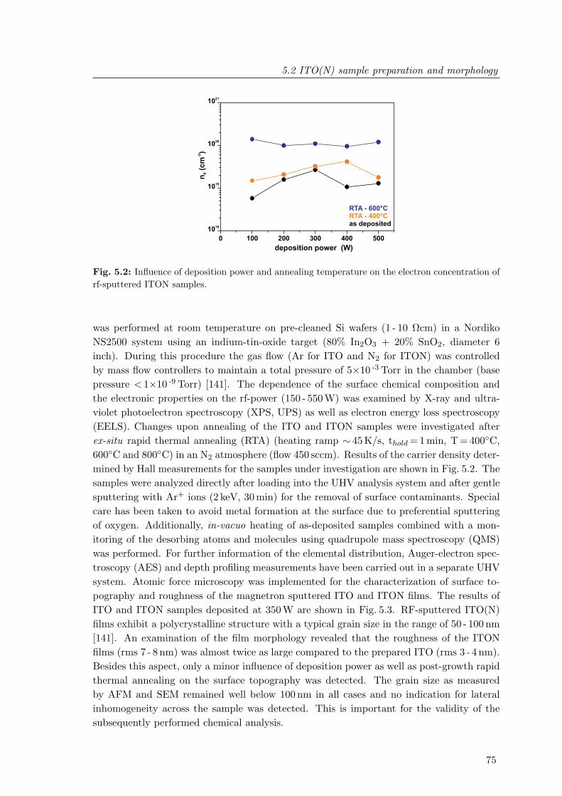
5.2 ITO(N) sample preparation and morphology
0 100 200 300 400 500
1810
1910
2010
2110
as deposited
RTA - 600°CRTA - 400°C
-3n
(c
m)
d
deposition power (W)
Fig. 5.2: Influence of deposition power and annealing temperature on the electron concentration ofrf-sputtered ITON samples.
was performed at room temperature on pre-cleaned Si wafers (1 - 10 Ωcm) in a NordikoNS2500 system using an indium-tin-oxide target (80% In2O3 + 20% SnO2, diameter 6inch). During this procedure the gas flow (Ar for ITO and N2 for ITON) was controlledby mass flow controllers to maintain a total pressure of 5×10 -3 Torr in the chamber (basepressure < 1×10 -9 Torr) [141]. The dependence of the surface chemical composition andthe electronic properties on the rf-power (150 - 550 W) was examined by X-ray and ultra-violet photoelectron spectroscopy (XPS, UPS) as well as electron energy loss spectroscopy(EELS). Changes upon annealing of the ITO and ITON samples were investigated afterex-situ rapid thermal annealing (RTA) (heating ramp ∼ 45 K/s, thold =1 min, T= 400C,600C and 800C) in an N2 atmosphere (flow 450 sccm). Results of the carrier density deter-mined by Hall measurements for the samples under investigation are shown in Fig. 5.2. Thesamples were analyzed directly after loading into the UHV analysis system and after gentlesputtering with Ar+ ions (2 keV, 30 min) for the removal of surface contaminants. Specialcare has been taken to avoid metal formation at the surface due to preferential sputteringof oxygen. Additionally, in-vacuo heating of as-deposited samples combined with a mon-itoring of the desorbing atoms and molecules using quadrupole mass spectroscopy (QMS)was performed. For further information of the elemental distribution, Auger-electron spec-troscopy (AES) and depth profiling measurements have been carried out in a separate UHVsystem. Atomic force microscopy was implemented for the characterization of surface to-pography and roughness of the magnetron sputtered ITO and ITON films. The results ofITO and ITON samples deposited at 350 W are shown in Fig. 5.3. RF-sputtered ITO(N)films exhibit a polycrystalline structure with a typical grain size in the range of 50 - 100 nm[141]. An examination of the film morphology revealed that the roughness of the ITONfilms (rms 7 - 8 nm) was almost twice as large compared to the prepared ITO (rms 3 - 4 nm).Besides this aspect, only a minor influence of deposition power as well as post-growth rapidthermal annealing on the surface topography was detected. The grain size as measuredby AFM and SEM remained well below 100 nm in all cases and no indication for lateralinhomogeneity across the sample was detected. This is important for the validity of thesubsequently performed chemical analysis.

Surface composition and electronic properties of indium tin oxide and oxynitride films
z-scale: 45 nm z-scale: 34 nm2x2 2µm 2
x2 2 µm
as deposited RTA - 600°C
z-scale: 68 nm z-scale: 69 nm2x2 2 µm
2x2 2 µm
ITO
N IT
O
Fig. 5.3: Atomic force micrographs of ITO and ITON films deposited by rf-sputtering at 350 W(left column: as deposited films, right column: films after rapid thermal annealing at 600C in N2).
5.3 Analysis of the incorporated nitrogen in ITON
In order to characterize the elemental distribution through the films as well as the surfacechemical composition of ITON and ITO samples prepared by rf-sputtering, X-ray photo-electron spectra and Auger-electron depth profiles have been recorded. The typical XPScore level peaks related to the detected elements have their maximum intensity at a bind-ing energy (BE) of 18.4 eV, 26.2 eV, 444.7 eV, 486.5 eV, and 530.2 eV for the In4d, Sn4d,In3d5/2, Sn3d5/2, and O1s state, respectively. As expected for samples that have beendeposited using N2, nitrogen was also detected in the films. However, it is not uniformlydistributed throughout the film, but concentrated in the first 40 - 50 nm. In deeper regionsthe N signal decreases below the detection limit of AES. Furthermore, for as-depositedITON and ITO as well as annealed ITO samples, a fairly homogeneous distribution of in-dium, tin and oxygen through the films is found [149]. This is not the case for annealedITON films (see Sect. 5.4). For a quantification of the amount of inserted nitrogen, theXPS core level spectra were fitted using Gauss-Lorentz functions, after the removal of aShirley-type background. The elemental proportions were calculated under the assumptionof a homogeneous distribution of all detected elements through the depth of information ofthe XPS measurement, taking into account the cross section, and asymmetry parameters ofthe detected spectral lines according to Yeh and Lindau [11]. In the case of film uniformity
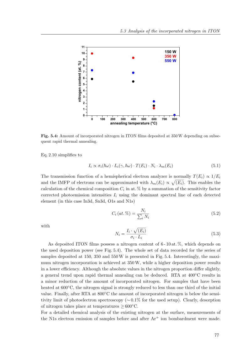
5.3 Analysis of the incorporated nitrogen in ITON
0 100 200 300 400 500 600 700 800
0
1
2
3
4
5
6
7
8
9
10
11
nit
rog
en
co
nte
nt
(at.
%)
annealing temperature (°C)
150 W350 W550 W
Fig. 5.4: Amount of incorporated nitrogen in ITON films deposited at 350W depending on subse-quent rapid thermal annealing.
Eq. 2.10 simplifies to
Ii ∝ σi(~ω) · Li(γ, ~ω) · T (Ei) ·Ni · λm(Ei) (5.1)
The transmission function of a hemispherical electron analyzer is normally T (Ei) ∝ 1/Ei
and the IMFP of electrons can be approximated with λm(Ei) ∝√
(Ei). This enables thecalculation of the chemical composition Ci in at.% by a summation of the sensitivity factorcorrected photoemission intensities Ii using the dominant spectral line of each detectedelement (in this case In3d, Sn3d, O1s and N1s)
Ci (at.%) =Ni∑i Ni
(5.2)
with
Ni =Ii ·√
(Ei)σi · Li
(5.3)
As deposited ITON films possess a nitrogen content of 6 - 10 at. %, which depends onthe used deposition power (see Fig. 5.4). The whole set of data recorded for the series ofsamples deposited at 150, 350 and 550W is presented in Fig. 5.4. Interestingly, the maxi-mum nitrogen incorporation is achieved at 350W, while a higher deposition power resultsin a lower efficiency. Although the absolute values in the nitrogen proportion differ slightly,a general trend upon rapid thermal annealing can be deduced. RTA at 400C results ina minor reduction of the amount of incorporated nitrogen. For samples that have beenheated at 600C, the nitrogen signal is strongly reduced to less than one third of the initialvalue. Finally, after RTA at 800C the amount of incorporated nitrogen is below the sensi-tivity limit of photoelectron spectroscopy (∼ 0.1% for the used setup). Clearly, desorptionof nitrogen takes place at temperatures ≥ 600C.For a detailed chemical analysis of the existing nitrogen at the surface, measurements ofthe N1s electron emission of samples before and after Ar+ ion bombardment were made.
Surface composition and electronic properties of indium tin oxide and oxynitride films
The results of the ITON sample series prepared at 350W and annealed at different temper-atures are presented in Fig. 5.5. In samples that have not undergone any treatment afterdeposition, the nitrogen atoms are found to exist in four different chemical states locatedat binding energies (BE) of 396.7 eV, 398.3 eV, 400.0 eV and ∼ 404.0 eV, respectively. Thestructure at 400.0 eV is only found for directly loaded samples and can be easily removed bythe Ar+ ion bombardment procedure. These states only exist at the surface and are typicalfor N-O bonds which are most likely formed due to oxidation of the samples at ambient con-ditions. The feature at 396.7 eV is attributed to nitrogen bound to metal atoms (N-In andN-Sn bonds). Unfortunately, the binding energy for both species is almost equal [150, 151]and a separation between these two contributions is beyond the energy resolution of themeasurement. The third structure at 398.3 eV is found to originate from oxynitride bonds[152], where oxygen as well as metal atoms are located in the surrounding of the nitrogenatom (InNxOy). The peak at 404.0 eV can originate from two possible sources: a) NO2
bonds or b) unbound nitrogen incorporated into the crystal structure. Since no indicationfor a NO2-related component was found in the O1s signal and the rf-sputtering process isperformed in a nitrogen plasma, this structure at 404.0 eV, in very good agreement witha nitridation study of III-V semiconductor surfaces, is assigned to incorporated unboundnitrogen that is formed due to the harsh deposition conditions. It is believed that thisunbound nitrogen is most likely located at interstitial sites [153, 154].Upon RTA, besides a small reduction of the total nitrogen concentration (see Fig. 5.4), nochanges concerning the nitrogen states were observed after annealing at 400C. Obviously,since the samples were exposed to ambient conditions prior to introduction to UHV, thesurfaces that have been characterized prior to ion bombardment still reveal a non-negligibleamount of N-O and oxynitride bonds. However, these features are present only due to reox-idation of the surface and are not related to changes induced by annealing of the films. Fortracking these changes, the ion bombarded surface measurements have to be analyzed. Asalready mentioned, the amount of nitrogen is strongly reduced after RTA at 600C. This ismainly related to the disappearance of the structure at 404.0 eV as well as almost the entireoxynitride component and parts from the metal-N signal, reducing the total N content toless than 2%. Finally, the rest of the nitrogen vanished after annealing at 800C.For a better analysis of the underlying desorption processes, ITON sample have also beenheated and analyzed in the UHV system. The same behavior was found for the disap-pearance of unbound nitrogen as well as oxynitride bonds. In order to understand theprocesses related to annealing of the ITON films, quadrupole mass spectroscopy (QMS)measurements were performed during annealing under UHV conditions. The desorption ofmolecules from the film as a function of temperature was analyzed in-situ during linearincrease of the sample temperature. It has to be mentioned that the used experimentalsetup is not sufficient for any quantitative desorption analysis as in thermal desorptionspectroscopy (TDS), since the QMS setup geometry (see Fig. 2.1) allows only analysis ofthe residual gas in the whole preparation chamber including effects of desorption fromparts of the manipulator assembly. Furthermore the heater assembly is not optimized forguaranteeing linear ramps at high heating rates. However, qualitative information aboutthe temperature-induced processes can still be obtained. The most striking effect duringramping up the temperature of a ITON sample is detected in the range between 550C and
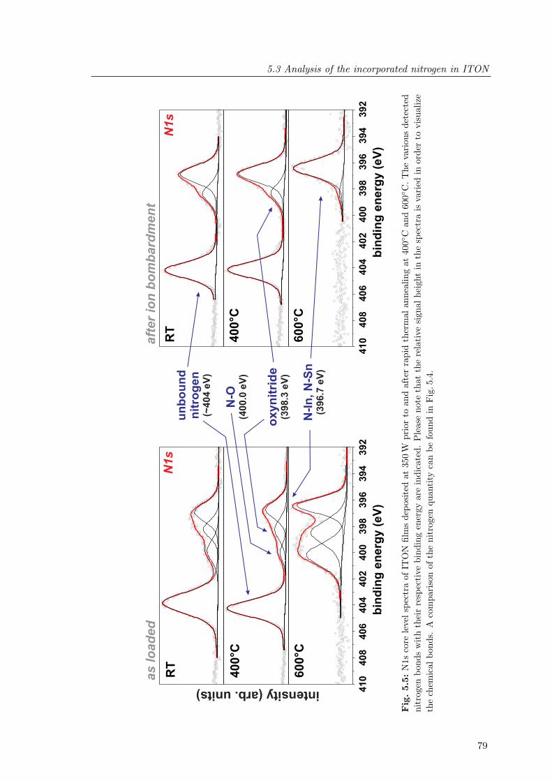
5.3 Analysis of the incorporated nitrogen in ITON
410
408
406
404
402
400
398
396
394
392
bin
din
g e
nerg
y (
eV
) b
ind
ing
en
erg
y (
eV
)
RT
400°C
600°C
N-I
n, N
-Sn
(396.7
eV
)
N-O
(400.0
eV
)
un
bo
un
dn
itro
gen
(~404 e
V)
N1s
as lo
ad
ed
a
fter
ion
bo
mb
ard
men
t
oxyn
itri
de
(398.3
eV
)
N1s
410
408
406
404
402
400
398
396
394
392
intensity (arb. units)
RT
400°C
600°C
Fig
.5.
5:N
1sco
rele
vels
pect
raof
ITO
Nfil
ms
depo
site
dat
350
Wpr
ior
toan
daf
ter
rapi
dth
erm
alan
neal
ing
at40
0C
and
600
C.T
heva
riou
sde
tect
edni
trog
enbo
nds
wit
hth
eir
resp
ecti
vebi
ndin
gen
ergy
are
indi
cate
d.P
leas
eno
teth
atth
ere
lati
vesi
gnal
heig
htin
the
spec
tra
isva
ried
inor
der
tovi
sual
ize
the
chem
ical
bond
s.A
com
pari
son
ofth
eni
trog
enqu
anti
tyca
nbe
foun
din
Fig
.5.4
.
Surface composition and electronic properties of indium tin oxide and oxynitride films
600C. An abrupt release of nitrogen takes place (rapid increase in signals m/e =14 and28), while only minor desorption of N2O was measured. Furthermore, no release of NO,NO2 or O2 was found. Any signal related to desorption of In or Sn is not expected at thesetemperatures and indeed could not be detected. This qualitative experimental finding is invery good agreement with the RTA induced changes observed in the N1s signal. Most of theincorporated unbound nitrogen is released at a certain temperature, while the oxynitridebonds are simultaneously broken. It should be noted that the temperature increase at thesample during the performed annealing in the UHV chamber was rather slow with a temper-ature ramp of ∆T/∆t∼ 15 K/min, the RTA process is much faster (∆T/∆t =45 K/s). Thisleads to incomplete nitrogen removal for 1 min RTA at 600C. Slightly higher temperatures(800C) are necessary to also remove the N-metal bonds.
5.4 Origin of the thermally induced changes in ITON films
Besides the already discussed release of nitrogen, several other impacts of rapid thermalannealing on the surface properties were found. The left side of Fig. 5.6 shows X-ray inducedAuger-electron spectra of ITON samples which were heated at various temperatures usingrapid thermal as well as UHV annealing. The measurements include the signals from theIn(MNN), Sn(MNN) and O(KLL) transition, respectively. For the RTA process, a strongincrease in the Sn(MNN) peak intensity was observed after annealing at T≥ 600C. Theamount of Sn is even higher when untreated ITON samples were annealed under UHVconditions. In this case, the signal intensity of Sn(MNN) is equal to the In(MNN) signal.This increase of the surface tin content is a strong indication for thermally induced surfacesegregation effects taking place above a certain temperature. AES depth profiles have beenmeasured in a separate chamber2 in order to evaluate the tin distribution within the firstlayers. The right part of Fig. 5.6 shows the depth profile of the ISn(MNN)/IIn(MNN) peakarea ratio for ITON films that have been treated by RTA at different temperatures. Foruntreated films and after 400C, a uniform Sn distribution was found through the first20 nm of the sample with a slight linear reduction of the Sn signal from the topmost layersinto the bulk. The only difference is a slightly higher average value at 400C. Upon RTAabove 600C, this compositional distribution is strongly modified. Now, the intensity ratioat the outermost surface is twice as high, decaying exponentially into the bulk to steadyvalues much lower compared to the untreated samples. This implies a strong segregationof tin atoms from the bulk of the material towards the surface. However, this process isnot related to the formation of a separate metallic tin phase at the surface, which wouldhave been visible as a second component of the Sn(3d) core level in XPS. It has to bementioned, that although such a drastic change of the ITON surface composition is foundat T≥ 600C, this behavior did not occur in the case of the ITO reference samples thathave been deposited using Ar as discharge gas.
2The AES system (Thermo Microlab 350) is equipped with a high spatial resolution field emission electron
beam column and a high energy resolution hemispherical analyzer. The primary electron beam (5 keV,
14 nA) had an incidence angle of 45 with respect to the surface normal and sputtering was carried out by
a conventional scanned ion beam gun (Ar+ ions, 1 keV, angle of incidence 47). The measurements were
performed by Ch. Mauder [155].

5.4 Origin of the thermally induced changes in ITON films
inte
ns
ity
(a
rb. u
nit
s)
Sn
(MN
N)
/ In
(MN
N)
rati
o
300 350 400 450 500 550
0 5 10 15 200.0
0.1
0.2
0.3
0.4
0.5
0.6
kinetic energy (eV) sputter depth (nm)
In(MNN)
O(KLL)Sn(MNN)
in situ annealing
850°C800°C
grown400°C600°C800°C
RTA
Fig. 5.6: Dependence of the In(MNN), Sn(MNN) and O(KLL) X-ray induced Auger-electron emis-sion as well as the Sn/In intensity ratio depth profile on annealing temperature of ITON thin films.
The presented experimental results of the XPS, AES and QMS analysis allow some conclu-sions on the origin of the observed changes of surface, electrical as well as optical propertiesof ITON thin films with respect to the differences of ITO reference samples deposited in anArgon plasma. The high electron concentration in indium tin oxide is caused by two fac-tors: a) the existence of a high content of oxygen vacancies and b) the incorporation of Snatoms at In crystal sites leading to the effect of n-type doping [156]. The amount of existingoxygen vacancies is mainly influenced by the deposition conditions during magnetron sput-tering (pressure, plasma power, sample temperature). In a highly reducing atmosphere,as used in this case for the deposition of ITO, the process conditions already result inthe formation of a high concentration of oxygen vacancies and hence in a very high elec-tron concentration (Hall measurements reveal nd∼ 2× 1020 cm-3) right from the beginning.Therefore, any treatment that aims to achieve a further reduction of the material, such asRTA in nitrogen atmosphere, is not very efficient and has only a minor effect on the carrierconcentration. A totally different behavior is found when the material is sputtered froman ITO target using N2 as the discharge gas. In this case nitrogen is incorporated into thematerial. As described above, a huge amount is inserted unbound at interstitial sites [154].Additionally, nitrogen is also incorporated in a high amount bound in the surrounding ofIn, Sn and O and it is supposed that nitrogen decorates the sites where typically oxygenatoms are missing resulting in trapping of electrons. This low amount of oxygen vacanciesleads to a noticeable lower carrier concentration in these samples (nd∼ 1019 cm-3). Since theincorporated nitrogen is not strongly bound, it can be released by thermal treatments. An-nealing above a critical temperature of ∼ 550C causes the desorption of the weakly boundnitrogen, which is completely removed after RTA at 800C for 1 minute. The remaining,previously N-decorated, sites can now act as a source for electrons, resulting in a strong
Surface composition and electronic properties of indium tin oxide and oxynitride films
increase of the carrier concentration of the material. In this way comparable values areachieved as for the Ar-sputtered ITO films. The driving force for these processes is relatedto the thermal instability observed for all indium-containing III-V compounds, such as InPand InN, which results in thermal decomposition at temperatures above 450C [71, 157].However, the thermally induced changes are not restricted to a simple outdiffusion of ni-trogen. The observation that Sn is additionally segregating from the bulk to the surfaceis an indicator for a rather complex rearrangement in the crystal structure. The enhancedSn concentration at the surface after annealing also contributes to the observed increase incarrier concentration and could be an explanation for the differences in the transmissionproperties of ITO and ITON films after RTA at 800C.It has to be mentioned that thermally induced Sn segregation and enhancement of thecarrier concentration has been observed in earlier works for ITO films which were preparedby magnetron sputtering [158] or using a sol-gel method [143]. The non-occurrence of theseeffects in the investigated ITO reference samples here is believed to be due to the usedstrongly reducing sputter conditions (Ar plasma). These conditions lead to a high degreeof non-stoichiometry along with the existence of a high amount of oxygen vacancies in thematerial, in contrast to ITON thin films that have been produced with the same sputteringparameters, but with nitrogen as the discharge gas.
5.5 Surface electronic properties of ITON
Analysis of the peak shape of the detected electron core level spectra (In3d, Sn3d and O1s)provides information about distinct changes in the surface electronic structure between thedifferent samples. The as-prepared ITON films exhibit narrow and totally symmetric peaksin XPS, while after annealing at T≥ 600C the structures are broadened and become asym-metric at the high binding energy side. A representative comparison of the two differentpeak shapes is presented for the In3d5/2 core level in Fig. 5.7. The changes in the O1s andSn3d5/2 signals are found to be identical. The asymmetry of the core levels has alreadybeen observed for ITO thin films in previous studies [143, 122, 159]. However, there is acontroversy about the origin of this structure. It is known that the high conductivity ofITO films is a result of two factors: a) the doping effect of the incorporated Sn atoms and b)the formation of oxygen vacancies which both act as donors [156]. While on the one hand,the asymmetry of the core level peaks might be attributed to an additional state related toa chemical shift due to the formation of oxygen vacancies [159], on the other hand Christouet al. discuss this behavior as an additional structure caused by the conduction electronplasmon excitation [122]. In an earlier publication about ITON, the asymmetric peak shapewas fitted using two Gauss-Lorentz peaks with a fixed G/L-ratio resulting in an energy sep-aration of 0.9 eV [155]. In the following an extensive study on many different samples wasperformed as a function of deposition power and annealing temperature. The asymmetryof the core levels occurs for samples that have a relatively high carrier concentration. In ac-cordance with earlier works on SnO2 and ITO, it can be explained by a screening response,in which the Coulomb potential of the core at an ionized atom creates a localized trap state[160, 122]. In this situation, two different final states are then accessible depending on

5.5 Surface electronic properties of ITON
449 448 447 446 445 444 443 442 441
449 448 447 446 445 444 443 442 441
inte
ns
ity
(a
rb. u
nit
s)
binding energy (eV)
In3d5/2
ITONas deposited
ITON after RTAat 600°C
0.45 eV
Fig. 5.7: Comparison of the In3d5/2 peak shape of a ITON sample prior to and after rapid thermalannealing. Details of the fit parameters are discussed in the text.
whether the localized state remains empty (giving an unscreened state) or is filled by trans-fer of an electron from the conduction band (resulting in a screened final state). The peakshape of the unscreened state at higher binding energy is much broader compared to thescreened state since it involves excitation of plasmons. This intrinsic plasmon excitation iscoupled with a certain relaxation rate and therefore lifetime broadening of this contributionis expected, which results in a Lorentzian peak profile [122, 160]. Hence, the different peakshapes of both components have to be taken into account for fitting. This leads to differentresults compared to the first approach. The energetic separation of the components is only0.45 eV as displayed in Fig. 5.7. In similarity to the above discussed aspects it has to bepointed out that the asymmetry in peak shape was found for as deposited and annealedITO films as well as ITON samples that have been annealed at or above 600C, giving onetype of sample state, while untreated and 400C RTA treated ITON films represent theother type with totally symmetric core levels peaks.In an alternative picture the high binding energy structure corresponds to an extrinsicplasmon satellite whose Lorentzian linewidth is determined by the conduction electronscattering rate [160]. The energetic separation of these two features can be used for a roughestimation of the carrier concentration. According to the correlation between electron con-centration and the bulk plasmon energy
ω2p =
(ne2
ε∞ε0m∗(n)
)(5.4)
n can be calculated. For the case of In2O3 and ITO the nonparabolicity of the conductionband has to be considered. Hence, the electron effective mass is dependent on the carrier
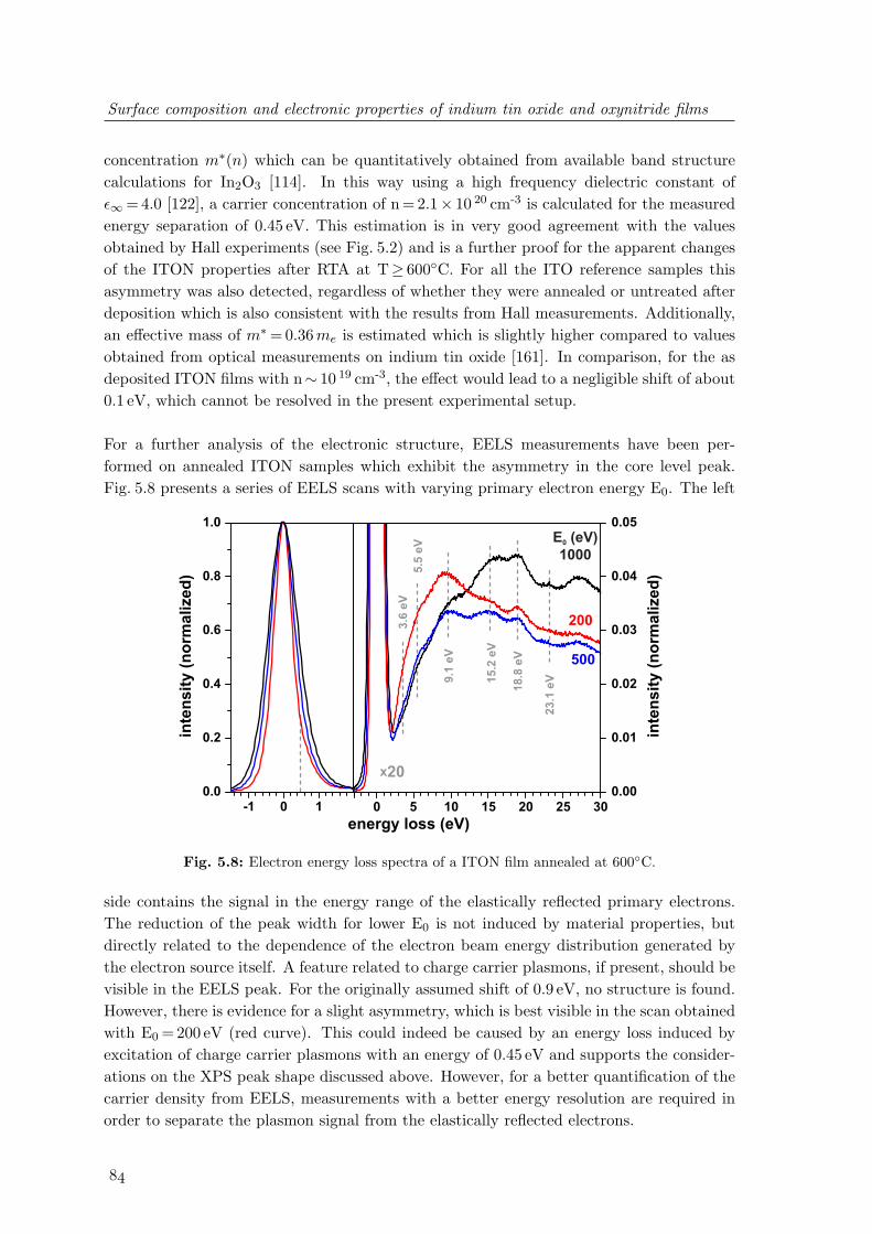
Surface composition and electronic properties of indium tin oxide and oxynitride films
concentration m∗(n) which can be quantitatively obtained from available band structurecalculations for In2O3 [114]. In this way using a high frequency dielectric constant ofε∞ = 4.0 [122], a carrier concentration of n =2.1× 10 20 cm-3 is calculated for the measuredenergy separation of 0.45 eV. This estimation is in very good agreement with the valuesobtained by Hall experiments (see Fig. 5.2) and is a further proof for the apparent changesof the ITON properties after RTA at T≥ 600C. For all the ITO reference samples thisasymmetry was also detected, regardless of whether they were annealed or untreated afterdeposition which is also consistent with the results from Hall measurements. Additionally,an effective mass of m∗ = 0.36 me is estimated which is slightly higher compared to valuesobtained from optical measurements on indium tin oxide [161]. In comparison, for the asdeposited ITON films with n∼ 10 19 cm-3, the effect would lead to a negligible shift of about0.1 eV, which cannot be resolved in the present experimental setup.
For a further analysis of the electronic structure, EELS measurements have been per-formed on annealed ITON samples which exhibit the asymmetry in the core level peak.Fig. 5.8 presents a series of EELS scans with varying primary electron energy E0. The left
0 5 10 15 20 25 30
E (eV)0
1000
500
200
0.00
0.01
0.02
0.03
0.04
0.05
0.0
0.2
0.4
0.6
0.8
1.0
in
ten
sit
y (
no
rma
lize
d)
energy loss (eV)
x20
in
ten
sit
y (
no
rma
lize
d)
-1 0 1
3.6
eV
5.5
eV
9.1
eV
15
.2 e
V
18
.8 e
V
23
.1 e
V
Fig. 5.8: Electron energy loss spectra of a ITON film annealed at 600C.
side contains the signal in the energy range of the elastically reflected primary electrons.The reduction of the peak width for lower E0 is not induced by material properties, butdirectly related to the dependence of the electron beam energy distribution generated bythe electron source itself. A feature related to charge carrier plasmons, if present, should bevisible in the EELS peak. For the originally assumed shift of 0.9 eV, no structure is found.However, there is evidence for a slight asymmetry, which is best visible in the scan obtainedwith E0 =200 eV (red curve). This could indeed be caused by an energy loss induced byexcitation of charge carrier plasmons with an energy of 0.45 eV and supports the consider-ations on the XPS peak shape discussed above. However, for a better quantification of thecarrier density from EELS, measurements with a better energy resolution are required inorder to separate the plasmon signal from the elastically reflected electrons.
5.5 Surface electronic properties of ITON
The high energy loss part of the EELS scans of an annealed ITON sample is presented inthe right part of Fig. 5.8. In order to evaluate the origin of the different features, a compari-son of measurements with different primary electron energies is useful, since this parameterallows a variation of the information depth in the measurements and hence allows a dis-crimination between surface and bulk effects. The dominant structures are located around9.1 eV, 15.2 eV and 18.8 eV. The first two structures are caused by plasmon losses inducedby the excitation of valence electrons, where the feature at 9.1 eV represents the surfaceplasmon and the one at 15.2 eV is related to excitation of electrons in the bulk [162, 163].This statement is supported by the fact that the relative intensities change when differentprimary electron energies are used. When E0 is reduced, the surface related states aretypically more pronounced due to the reduced electron inelastic mean free path. The twopeaks at 18.8 eV and 23.1 eV are attributed to transitions from the In4d semi-core level tounoccupied states in the conduction band (In4d→CB), consistent with measurements onindium oxide [162, 163]. Since the annealed ITON films also have a high concentration oftin at the surface, the same type of interband transitions from the Sn4d level (Sn4d→CB)also contribute to the total spectrum, in agreement with EELS results on the oxidationof Sn [164]. There are also structures at higher energy values which are mainly relatedto multiples and combinational losses. In addition to these well-pronounced structures, adetailed analysis of the spectra reveals that there are further features in the rising edgebetween 2 eV and 7 eV. Two structures at 3.6 eV and 5.5 eV are identified (best visiblein the scan with E0 =500 eV), which have also been found, but not discussed in previousmeasurements on ITO [165]. These spectral features are due to interband transitions fromoccupied states in the valence band to empty conduction band states above the Fermi levelEF [163, 164].
UPS measurements reveal no clear trend in the work function of the different ITO andITON samples. All values vary within the range of 4.2 eV± 0.1 eV, which have been de-termined from the onset of the secondary electron peak. The valence band distribution ofITO and ITON samples measured using He I and He II radiation are presented in Fig. 5.9.For the ITO thin films, the valence band maximum determined by extrapolation of thetrailing edge to zero is located 3.4 eV below EF , while it is slightly shifted to 3.2 eV for theuntreated and annealed ITON films. Both films exhibit structures in the valence band at4.5 eV and 8.8 eV, comparable to indium oxide surfaces, as well as the In4d level at 18.4 eV,which agrees with the XPS results and is typical for ITO films [166]. A slight differencebetween ITO and ITON is detected in the energy range between 1 eV and 3 eV, which ismainly related to defect states in the band gap. For ITON, a higher signal is detectedaround ∼ 2.7 eV which is probably induced by the incorporated nitrogen atoms. A com-parison with the valence band distribution of InN (see chapter 3 and [65]), where the firstintensity maximum is located in this energy range, supports this suggestion.Annealing of ITON at T≥ 600C also results in changes in the valence band distribution.An increase in intensity between 5 eV and 8 eV is observed with a slightly more pronouncedstructure at 5.8 eV. This effect can be explained by the surface segregation of tin at highertemperatures. The higher the Sn content on the surface, the more are the SnO2-like statesexistent in the valence band, and located at a slightly higher binding energy relative to theIn2O3-like states [167].

Surface composition and electronic properties of indium tin oxide and oxynitride films
10 9 8 7 6 5 4 3 2 1 0
inte
ns
ity
(a
rb. u
nit
s)
UPS (He II)hν = 40.8 eV
UPS (He I)hν = 21.2 eV
10 9 8 7 6 5 4 3 2 1 0
binding energy (eV)
binding energy (eV)
ITON (as deposited)
ITO (as deposited)ITON (RTA at 600°C)
Fig. 5.9: Comparison of the valence band photoemission of ITO and ITON films measured usingusing He I (hν =21.2 eV) and He II (hν =40.8 eV) radiation.
In conclusion it can be stated that the incorporation of nitrogen during magnetron sputter-ing of ITO results in interesting new material properties. The changes related to the use ofnitrogen as process gas could be identified to a certain degree using electron spectroscopymeasurements. A correlation between the optical and electrical properties of the materialto the surface properties was found. It could be directly shown that the incorporated ni-trogen plays an important role in the physical properties of these ITON films. However,the thermal instability of the material has to be taken into account for any high temper-ature processes required for device fabrication. Nevertheless, the extended optical windowof ITON after RTA could still be useful in future optoelectronic applications.
Chapter 6
Summary and Outlook
Several aspects of the dependence of preparation conditions on structural properties, sur-face composition as well as surface electronic structure of different indium compounds havebeen investigated using surface sensitive techniques such as photoelectron, Auger-electronand electron energy loss spectroscopy as well as scanning force microscopy and reflectionhigh-energy electron diffraction. This includes in particular, the electron density of bulkand surface states of clean InN(0001) films, the properties of polycrystalline indium oxidethin films and their interaction with oxidizing gases for the implementation in ozone de-tectors as well as changes of the material properties due to incorporation of nitrogen intotransparent, highly conductive indium tin oxide films.
Since indium nitride films are very reactive towards ambient gases, the approach to combinethe MBE growth of InN(0001) films with the examination of the surface electronic structurein one UHV system was successfully followed for the first time.A clear correlation between the In/N flux ratio and the surface stoichiometry and mor-phology is found. In the case of a high nitrogen supply, excess nitrogen is incorporatedinto the material and the growth is 3-dimensional. Additionally, the formation of a smallproportion of cubic InN was noticed after growth at N-rich conditions and low substratetemperatures. The crystal quality and morphology is improved in the case of slightly In-richgrowth conditions during MBE due to the accumulation of indium layers at the surface andthe consequently enhanced diffusion of the reactants in this case.For the characterization of the surface electronic structure of stoichiometric InN(0001) films,the growth parameters have been optimized in order to assure the absence of any excessmaterial. Taking into account the low film thickness of < 300 nm, a good crystalline qual-ity could be achieved. The lowest measured bulk electron concentration was 8×1018 cm-3,which is about one order of magnitude higher than the best values reported in the literaturefor films exceeding a thickness of 1 µm.From the results of photoelectron spectroscopy measurements using different excitationsources, it can be stated that the measured occupied electron states of InN are in very goodagreement with theoretical calculations of the bulk density of states. On the other side,for the unoccupied InN states determined from fine structures in the secondary electroncascade, a qualitative agreement between experimental and theoretical data was found, butthe observed energy shift cannot be explained at present.

Summary and Outlook
Depending on the growth temperature, the surface atoms tend to arrange in two differ-ent reconstructions at the InN(0001) surface: (2×2) or (
√3 ×
√3)R30. Although, the
(√
3 ×√
3)R30 structure has been already reported in the literature, the presented re-sults exhibit the first experimental study that determines the impacts of the formationof a surface reconstruction on the electronic properties of indium nitride. The indiumadatom arrangement leads to distinct electronic states inside the band gap of InN, directlylocated at the Fermi edge for (2×2) reconstructed films or 0.75 eV below EF in the caseof a (
√3×
√3)R30 structure. The experimental results agree very well with the available
theoretical calculations of InN surface structures.For stoichiometric InN films that have been examined in-situ after MBE growth, a strongelectron accumulation is observed at the surface. In this case, oxidation of the surface dueto contact with O2 can be excluded as reason for this characteristic. The formed surfacestates as well as other intrinsic donor-like states have to be considered as source of electronsin the accumulation layer. Furthermore it was preliminary found that the interaction ofclean InN(0001) surfaces with O2 leads to the adsorption of oxygen, but has no influenceon the valence band bending and the electron accumulation layer.
Indium oxide films were investigated in order to study the processes related to the highsensitivity of polycrystalline InOx in detecting ozone. For this purpose, the surface char-acteristics of externally MOCVD grown In2O3 layers were intensively examined dependingon their crystalline properties that are mainly controlled by the temperature regime duringgrowth.For growth temperatures above 400C, the resulting polycrystalline layers consist of eitherflat or pyramidal shaped islands, depending on the orientation of the grown film. Theselayers are not very sensitive towards ozone. In2O3 films with bixbyite structure in differentorientation ((001) and (111)) or rhombohedral (0001) structure, exhibit similar chemicalproperties.Careful examination of the valence band states supports the results from recently publishedstudies that the commonly accepted band gap value of In2O3 of 3.6 eV is too large and thecorrect gap lies around 3 eV. This has also consequences on the interpretation of the surfaceband distribution. The reduced gap would lead to almost flat band conditions instead ofthe normally assumed strong upward band bending induced by an electron depletion layerat indium oxide surfaces.
Chemical vapor deposition performed at temperatures as low as 200C using trimethylindiumand water, results in the formation of porous nanocrystalline indium oxide films (particlesize 7 - 8 nm) that exhibit a very high sensitivity towards ozone and can be implementedin O3 sensors. This characteristic is mainly related to the existence of a very high densityof defects at the nanocrystallite surface acting as reactive adsorption centers. The ozonesensor principle is based on the reversible adsorption of oxygen species at these reactivecenters, resulting in a charge transfer from the substrate towards the adsorbate, as well asthe UV radiation or thermally induced desorption which results in a strong variation of thefilm resistance.After O3 oxidation, an unexpected shift of the valence band away from the Fermi levelis detected, although the electrical characteristics point towards a reduction of the carrier
concentration. Based upon the photoelectron spectroscopy data, a model is proposed thatexplains the observations by an altered band gap at the vicinity of the surface, which isinduced by the adsorption of oxygen species.The interaction with O3 is based on the dissociation of the molecule and adsorption inthe form of negatively charged oxygen ions due to electron transfer from the indium oxidetowards the adsorbate. The same adsorbate is formed when the surface comes into contactwith water. This observation explains the reduced sensitivity of the ozone sensor devices,when operated under humid conditions.
The incorporation of nitrogen into indium tin oxide by rf magnetron sputtering in N2 at-mosphere was characterized by X-ray photoelectron spectroscopy. Depending on the usedplasma power, up to 10% of nitrogen is inserted into the films, which is bound in differentchemical states. The formation of N-In, N-Sn as well as N-O bonds was verified. Addition-ally, a large portion of the incorporated nitrogen is inserted into the films without formingchemical bonds with indium, tin or oxygen. In accordance to studies on the nitridation ofInP, InAs and InSb, this phase is attributed to nitrogen that is embedded at interstitialsites.The incorporation of nitrogen leads to a decoration of oxygen vacancies in the material andconsequently to a reduction of the electron concentration by about one order of magnitudecompared to conventional Ar-sputtered ITO films.As for all indium compounds, the thermal instability of the material is one major aspect ofthe properties of these materials. The inserted nitrogen desorbs out of the film above 550C.Simultaneously the segregation of tin towards the surface occurs. Both processes result ina strong increase in the carrier concentration in the material. Hence, post-processing byrapid thermal annealing leads to improved electrical properties (higher conductivity andhigh electron mobility). As a consequence, the optical transmission in the near UV regionis increased for ITON films compared to conventionally Ar sputtered ITO films.
The performed investigations resulted in new insights to open questions about the prop-erties of indium compounds. Nevertheless, there are still many unsolved problems thatrequire further studies on these materials.The achieved experience in the preparation of clean and well-defined InN surfaces withpronounced reconstructions allows even deeper fundamental investigations on this specialsemiconductor. For this purpose, further improvement of the material properties (espe-cially crystallinity, morphology and electron concentration) will be crucial and is expectedto be realized by increasing the thickness of the grown films. Especially smooth surfaceswould allow angle-dependent photoelectron spectroscopy measurements in order to mapthe k-dependence of the electronic states. Furthermore, examination of the local structuraland electric properties by scanning tunneling microscopy/spectroscopy measurements isencouraged.The realized capability for in-situ characterization of MBE grown films allows further stud-ies of the initial stages of interaction with different atoms or molecules in order to investi-gate surface reactions on an atomic level, which is not possible on samples that have been

Summary and Outlook
exposed to ambient conditions. This would include extensive studies on the influence ofdifferent adsorbates, such as alkali-atoms or gaseous materials.In particular, for the consideration of indium nitride based transistor devices, characteriza-tion of interface and band alignment properties of InN towards possible gate and contactmaterials will be one important task for future experiments. The technological equipmentin the ZMN facilitates these measurements and especially the study of the InN/In2O3 in-terface can be relatively easy realized in the UHV growth and surface analysis system.The investigation of the surface electronic structure should be further expanded to N-polarity or non-polar InN films that can be grown on special substrates. Of great impor-tance is a confirmation or exclusion of the theoretically predicted absence of the electronaccumulation layer at a- and m-plane InN surface prepared under stoichiometric conditions.
Surface studies on defect rich nanocrystalline indium oxide films enabled a qualitative de-scription of the processes related to ozone oxidation and UV-induced reduction of thesurface. The presented measurements were performed close to the actual environment thesensor surfaces are exposed to during operation. However, these investigations can only inparts contribute to an overall description of the underlying processes that define the ozonesensor characteristics. This is related to the complexity of the system, where several aspectshave to be considered such as the structural, compositional and electronic features of thefilms. It is worth to study several aspects separately in order to distinguish between the dif-ferent influences. This includes to switch to epitaxial or single crystal In2O3 surfaces for theexamination of the surface reactions, and to define reference experiments as is typically donein studies on catalytic materials. For the gas interaction processes, coverage-dependent sur-face spectroscopy measurements will refine the proposed models and are encouraged for thenear future. Especially the implementation of extremely adsorbate sensitive experimentaltechniques such as high-resolution electron energy loss spectroscopy and metastable impactelectron spectroscopy are expected to give further insight into the dissociation processes ofozone and water at the surface.It has to be mentioned that the performed experiments as well as the measurements pro-posed for the future strongly rely on theoretical studies of possible stable adsorbate con-figurations on In2O3 surfaces. Hopefully, the progress in computation speed as well astheoretical approaches result in supporting information on the surface properties of thecomplex system indium oxide in the near future.
The presented studies have established a better knowledge of the surface properties ofInN(0001), polycrystalline indium oxide as well as indium tin oxynitride thin films. Mostof the aspects discussed here are of fundamental character and do not directly lead intonew (opto)electronic applications. However, the results can contribute to a better basicunderstanding of indium compounds and help to conceive the fundamental material char-acteristics as well as processes during film preparation or device operation.Hopefully, some of these indium based materials will lead to improvement of existing or toeven new devices in the near future. The transfer from first demonstrators to the realiza-tion of commercial LT-InOx based ozone sensors, would give the chance for a wide-range

control of the O3 concentration in the environment and prevent people to be exposed toharmful doses. Indium nitride based applications are still a perspective, but large efforts areput into the study and development of e.g. extremely fast transistors as well as terahertzemitters. A successful implementation of the material requires further improvement of thefilm quality and the recently started transition from pure material properties based studiestowards applied investigations.Perspectively, the implementation of annealed ITON layers could improve the performanceof devices that rely on transparent conductive oxides, since the window of transparencycan be shifted further into the UV. Special impact is expected on the quality of ohmic con-tacts on p-type nitride films, since the incorporated nitrogen can lead to improved interfaceproperties upon annealing.


Bibliography
[1] J.E. Ayers. Heteroepitaxy of Semiconductors - Theory, Growth and Characterization.CRC Press, 2007.
[2] K. Oura, V.G. Lifshits, A.A. Saranin, A.V. Zotov, and M. Katayama. Surface Science- An Introduction. Advanced Texts in Physics. Springer, 2003.
[3] A. Ichimiya and P.I. Cohen. Reflection high-energy electron diffraction. CambridgeUniversity Press, 2004.
[4] W. Braun. Applied RHEED - Reflection High-Energy Electron Diffraction DuringCrystal Growth. Springer, 1999.
[5] M. Cardona and L. Ley. Photoemission in Solids, General Principles, volume 26 ofTopics in Applied Physics. Springer Verlag, Berlin, 1978.
[6] D. Briggs and M.P. Seah. Auger and X-ray Photoelectron Spectroscopy, volume 1 ofPractical Surface Analysis. John Wiley & Sons, New York, 2nd edition, 1990.
[7] S. Hufner. Photoelectron Spectroscopy, Principles and Applications, volume 82 ofSpringer Series in Solid-State Sciences. Springer Verlag, Berlin, 1996.
[8] M. Henzler and W. Gopel. Oberflachenphysik des Festkorpers. Teubner, Stuttgart,2nd edition, 1994.
[9] M.P. Seah and W.A. Dench. Quantitative Electron Spectroscopy of Surfaces: AStandard Data Base for Electron Mean Free Paths in Solids. Surface and InterfaceAnalysis, 1(1):2–11, 1979.
[10] S. Tanuma, C.J. Powell, and D.R. Penn. Surf. Interface Anal., 20:77, 1993.
[11] J.J. Yeh and I. Lindau. Atomic Data and Nuclear Data Tables, 32:1, 1985.
[12] W. Monch. Semiconductor Surfaces and Interfaces, volume 26 of Springer Series inSurface Science. Springer, 3rd edition, 2001.
[13] R.E. Thomas, A. Shih, and G.A. Haas. Surf. Sci., 75:239, 1978.
[14] J. Schafer, R. Schoppe, J. Holzl, and R. Feder. Surf. Sci., 107:290, 1981.
[15] T. Takahashi, H. Tokailin, and T. Sagawa. Phys. Rev. B, 32:8317, 1985.
[16] H. Luth. Surfaces and Interfaces of Solids. Springer, 1993.
BIBLIOGRAPHY
[17] V.M. Polyakov, A. Elbe, J. Wu, G.J. Lapeyre, and J.A. Schaefer. Phys. Rev. B,54:2010, 1996.
[18] T. Balster. Untersuchungen an reinen und mit Wasserstoff bedeckten SiC(100)-Oberflachen mit Hochaufgeloster Elektonenenergieverlususpektroskopie. Dissertation,Institute of Physics, TU Ilmenau, 1999.
[19] X-ray Monochromators XM500 and XM1000 users guide, Version 2.2. Omicron
Nanotechnology GmbH, 2003.
[20] Instruction Manual VUV Discharge Lamp HIS13, Version 1.7. Focus GmbH(Omicron), 1996.
[21] D. Sarid. Scanning Force Microscopy. Oxford University Press, 1994.
[22] R. Wiesendanger (ed.). Scanning Probe Microscopy. Nanoscience and Technology.Springer, 1998.
[23] M. Himmerlich. Photoelectron Emission Microscopy and Photoelectron Spectroscopyof Ge on Si, InN and InP. Diplom thesis, Institute of Physics, TU Ilmenau, 2005.
[24] H. Morkoc. Handbook of Nitride Semiconductors and Devices, volume 1-3. Wiley-VCH, 2008.
[25] M.S. Shur S.K. O’Leary, B.E. Foutz and L.F. Eastman. Appl. Phys. Lett., 87:222103,2005.
[26] V.M. Polyakov and F. Schwierz. Appl. Phys. Lett., 88:032101, 2006.
[27] T.L. Tansley and C. Foley. J. Appl. Phys., 59:3241, 1986.
[28] A. Wakahara, T. Tsuchia, and A. Yoshida. J. Cryst. Growth, 99:385, 1990.
[29] W.E. Hoke, P.J. Lemonias, and D.G. Weir. J. Cryst. Growth, 111:1024, 1991.
[30] S. Yamaguchi, M. Kariya, S. Nitta, T. Takeuchi, C. Wetzel, H. Amano, and I. Akasaki.J. Appl. Phys., 85:7682, 1999.
[31] H. Lu, W.J. Schaff, J. Hwang, H. Wu, W. Yeo, A. Pharkya, and L.F. Eastman. Appl.Phys. Lett., 77:2548, 2000.
[32] B. Maleyre, O. Briot, and S. Ruffenach. J. Cryst. Growth, 269:15, 2004.
[33] C.H. Swartz, R.P. Tomkins, T.H. Myers, H. Lu, and W.J. Schaff. phys. stat. sol. (c),2:2250, 2005.
[34] V. Lebedev, V. Cimalla, J. Pezoldt, M. Himmerlich, S. Krischok, J.A. Schae-fer, O. Ambacher, F.M. Morales, J.G. Lozano, and D. Gonzalez. J. Appl. Phys.,100:094902, 2006.
[35] J. Wu and W. Walukiewicz. Superlattices Microstruct., 34:63, 2003.
[36] K.S.A. Butcher and T.L. Tansley. Superlattices Microstruct., 38:1, 2005.
BIBLIOGRAPHY
[37] B. Monemar, P.P. Paskov, and A. Kasic. Superlattices Microstruct., 38:38, 2005.
[38] V.Y. Davydov, A.A. Klochikhin, R.P. Seisyan, V.V. Emtsev, S.V. Ivanov SV, F. Bech-stedt, J. Furthmuller, H. Harima, V. Mudryi, J. Aderhold, O. Semchinova, andJ. Graul. phys. stat. sol. (b), 229:R1, 2002.
[39] W. Walukiewicz, J.W. Ager, K.M. Yu, Z. Liliental-Weber, J. Wu, S.X. Li, R.E. Jones,and J.D. Denlinger. J. Phys. D, 39:R83, 2006.
[40] R. Goldhahn, P. Schley, A.T. Winzer, G. Gobsch, V. Cimalla, O. Ambacher, M. Rakel,C. Cobet, N. Esser, H. Lu, and W.J. Schaff. phys. stat. sol (a), 203:42, 2006.
[41] J. Furthmuller, P.H. Hahn, F. Fuchs, and F. Bechstedt. Phys. Rev. B, 72:205106,2005.
[42] D. Fritsch, H. Schmidt, and M. Grundmann. Phys. Rev. B, 69:165204, 2004.
[43] V. Cimalla, V. Lebedev, F.M. Morales, R. Goldhahn, and O. Ambacher. Appl. Phys.Lett., 89:172109, 2006.
[44] Y.-S. Lin, S.-H. Koa, C.-Y. Chan, S.S.H. Hsu, H.-M.Lee, and S. Gwo. Appl. Phys.Lett., 90:142111, 2007.
[45] E. Trybus, G. Namkoong, W. Henderson, S. Burnham, W.A. Doolittle, M. Cheung,and A. Cartwright. J. Cryst. Growth, 288:218, 2006.
[46] H. Lu, W.J. Schaff, and L.F. Eastman. J. Appl. Phys., 96:3577, 2004.
[47] R. Ascazubi, I. Wilke, K. Denniston, H. Lu, and W.J. Schaff. Appl. Phys. Lett.,84:4810, 2004.
[48] G.D. Chern, E.D. Readinger, H.G. Shen, M. Wraback, C.S. Gallinat, G. Koblmuller,and J.S. Speck. Appl. Phys. Lett., 89:141115, 2006.
[49] K.A. Rickert, A.B. Ellis, F.J. Himpsel, H. Lu, W. Schaff, J.M. Redwing,F. Dwikusuma, and T.F. Kuech. Appl. Phys. Lett., 82:3254, 2003.
[50] S. Krischok, V. Yanev, O. Balykov, M. Himmerlich, J.A. Schaefer, R. Kosiba, G. Ecke,I. Cimalla, V. Cimalla, O. Ambacher, H. Lu, W.J. Schaff, and L.F. Eastman. Surf.Sci., 566-568:849, 2004.
[51] L.F.J. Piper, T.D. Veal, M. Walker, I. Mahboob, C.F. McConville, H. Lu, and W.J.Schaff. J. Vac. Sci. Technol. A, 23:617, 2005.
[52] T.D. Veal, P.D.C. King, P.H. Jefferson, L.F.J. Piper, C.F. McConville, H. Lu, W.J.Schaff, P.A. Anderson, S.M. Durbin, D. Muto, H. Naoi, and Y. Nanishi. Phys. Rev.B, 76:075313, 2007.
[53] L.F.J. Piper, T.D. Veal, P.H. Jefferson, C.F. McConville, F. Fuchs, J. Furthmuller,F. Bechstedt, H. Lu, and W.J. Schaff. Phys. Rev. B, 72:245319, 2005.
BIBLIOGRAPHY
[54] M. Draxler, M. Walker, and C.F. McConville. Nucl. Instrum. Methods Phys. Res. B,249:886, 2006.
[55] I. Mahboob, T.D. Veal, C.F. McConville, H. Lu, and W.J. Schaff. Phys. Rev. Lett.,92:036804, 2004.
[56] T.D. Veal, L.F.J. Piper, I. Mahboob, H. Lu, W.J. Schaff, and C.F. McConville. phys.stat. sol. (c), 2:2246, 2005.
[57] H. Lu, W.J. Schaff, L.F. Eastman, and C.E. Stutz. Appl. Phys. Lett., 82:1736, 2003.
[58] C.G. Van de Walle and J. Neugebauer. Nature, 423:626, 2003.
[59] S.X. Li, K.M. Yu, J. Wu, R.E. Jones, W. Walukiewicz, J.W. Ager, W. Shan, E.E.Haller, H. Lu, and W.J. Schaff. Phys. Rev. B, 71:161201, 2005.
[60] P.D.C. King, T.D. Veal, P.H. Jefferson, S.A. Hatfield, L.F.J. Piper, C.F. McConville,F. Fuchs, J. Furthmuller, F. Bechstedt, H. Lu, and W.J. Schaff. Phys. Rev. B,77:045316, 2008.
[61] D. Segev and C.G. Van de Walle. Europhys. Lett., 76:305, 2006.
[62] C.G. Van de Walle and David Segev. J. Appl. Phys., 101:081704, 2007.
[63] P.D.C. King, T. D. Veal, C.F. McConville, F. Fuchs, J. Furthmuller, F. Bechstedt,P. Schley, R. Goldhahn, J. Schormann, D.J. As, K. Lischka, D. Muto, H. Naoi,Y. Nanishi, H. Lu, and W.J. Schaff. Appl. Phys. Lett., 91:092101, 2007.
[64] E. Calleja, J. Grandal, M.A. Sanchez-Garcıa, M. Niebelschutz, V. Cimalla, andO. Ambacher. Appl. Phys. Lett., 90:262110, 2007.
[65] M. Himmerlich, S. Krischok, V. Lebedev, O. Ambacher, and J.A. Schaefer. J. Cryst.Growth, 306:6, 2007.
[66] V. Cimalla, M. Niebelschutz, G. Ecke, V. Lebedev, O. Ambacher, M. Himmerlich,S. Krischok, J.A. Schaefer, H. Lu, and W.J. Schaff. phys. stat. sol. (a), 203:59, 2006.
[67] R.E. Jones, K.M. Yu, S.X. Li, W. Walukiewicz, J.W. Ager, E.E. Haller, H. Lu, andW.J. Schaff. Phys. Rev. Lett., 96:125505, 2006.
[68] A. Eisenhardt. Molekularstrahlepitaxie und Oberflachenanalyse von In-polarem InN.Diplom thesis, Institute of Physics, TU Ilmenau, 2008.
[69] E. Dimakis, E. Iliopoulos, K. Tsagaraki, and A. Georgakilas. Appl. Phys. Lett.,86:133104, 2005.
[70] E. Dimakis, E. Iliopoulos, K. Tsagaraki, and A. Georgakilas. phys. stat. sol. (a),203:1686, 2006.
[71] C.S. Gallinat, G. Koblmuller, J.S. Brown, and J.S. Speck. J. Appl. Phys., 102:064907,2007.
BIBLIOGRAPHY
[72] D. Segev and C.G. Van de Walle. Surf. Sci. Lett., 601:L15, 2007.
[73] K.S.A. Butcher, A.J. Fernandes, P.P.-T.Chen, M. Wintrebert-Fouquet, H. Timmers,S.K. Shrestha, H. Hirshy, R.M. Perks, and B.F. Usher. J. Appl. Phys., 101:123702,2007.
[74] Y.G. Cao, S.H. Xu, W. Lu, X.Q. Dai, Y.F. Chan, N. Wang, Y. Liu, H.S. Wu, M.H.Xie, and S.Y. Tong. Phys. Rev. B, 71:155322, 2005.
[75] C.K. Gan and D.J. Srolovitz. Phys. Rev. B, 74:115319, 2006.
[76] V. Cimalla, Ch. Forster, G. Kittler, I. Cimalla, R. Kosiba, G. Ecke, O. Ambacher,R. Goldhahn, S. Shokhovets, A. Georgakilas, H. Lu, and W.J. Schaff. phys. stat. sol.(c), 0:2818, 2003.
[77] E. Dimakis, E. Iliopoulos, K. Tsagaraki, A. Adikimenakis, and A. Georgakilas. Appl.Phys. Lett., 88:191918, 2006.
[78] P. Schley, R. Goldhahn, A.T. Winzer, G. Gobsch, V. Cimalla, O. Ambacher, H. Lu,W.J. Schaff, M. Kurouchi, Y. Nanishi, M. Rakel, C. Cobet, and N. Esser. Phys. Rev.B, 75:205204, 2007.
[79] R. Goldhahn. Acta Phys. Pol. A, 104:123, 2003.
[80] L.F.J. Piper, T.D. Veal, I. Mahboob, C.F. McConville, H. Lu, and W.J. Schaff. Phys.Rev. B, 70:115333, 2004.
[81] R.P. Bhatta, B.D. Thoms, M. Alevli, and N. Dietz. Surf. Sci. Lett., 601:L120, 2007.
[82] K. Klockner, V. Polyakov, M. Himmerlich, A. Eisenhardt, R.J. Koch, S.I.-U. Ahmed,S. Krischok, and J.A. Schaefer. Accumulation layer density profile and bulk electronconcentration of MBE grown InN(0001) (to be published).
[83] P.D.C. King, T.D. Veal, C.F. McConville, F. Fuchs, J. Furthmuller, F. Bechstedt,J. Schormann, D.J. As, K. Lischka, H. Lu, and W.J. Schaff. Phys. Rev. B, 77:115213,2008.
[84] M. Rakel, C. Cobet, N. Esser, F. Fuchs, F. Bechstedt, R. Goldhahn, W.G. Schmidt,and W.J. Schaff. Phys. Rev. B, 77:115120, 2008.
[85] L.F.J. Piper, L. Colakerol, T. Learmonth, P.-A. Glans, K.E. Smith, F. Fuchs,J. Furthmuller, F. Bechstedt, T.-C. Chen, T.D. Moustakas, and J.-H. Guo. Phys.Rev. B, 76:245204, 2007.
[86] F. Fuchs, J. Furthmuller, F. Bechstedt, M. Shishkin, and G. Kresse. Phys. Rev. B,76:115109, 2007.
[87] D. Segev, A. Janotti, and C.G. Van de Walle. Phys. Rev. B, 75:035201, 2007.
[88] F. Fuchs. private communication.

BIBLIOGRAPHY
[89] D. Muto, T. Araki, H. Naoi, F. Matsuda, and Y. Nanishi. phys. stat. sol. (a), 202:773,2005.
[90] R. Gutt. Plasma Assisted Molecular Beam Epitaxy of Gallium Nitride on SiliconCarbide Substrates. Diplom thesis, Institute of Physics, TU Ilmenau, 2008.
[91] T.D. Veal, P.D.C. King, M. Walker, C.F. McConville, H. Lu, and W.J. Schaff. PhysicaB, 401-402:351, 2007.
[92] S.-H. Lee, Y.-S. Kim, and Y.-C. Chung. Jap. J. Appl. Phys., 46:6205, 2007.
[93] V. Lebedev, Ch. Y. Wang, V. Cimalla, S. Hauguth, T. Kups, M. Ali, G. Ecke, M. Him-merlich, S. Krischok, J.A. Schaefer, O. Ambacher, V. M. Polyakov, and F. Schwierz.J. Appl. Phys., 101:123705, 2007.
[94] T. Seiyama (ed.). Chemical Sensor Technology. Elsevier, 1988-1991.
[95] M. Batzill and U. Diebold. Phys. Chem. Chem. Phys., 9:2307, 2007.
[96] N. Barsan and U. Weimar. J. Electroceram., 7:143, 2001.
[97] M.Z. Atashbar, B. Gong, H.T. Sun, W. Wlodarski, and R. Lamb. Thin Solid Films,354:222, 1999.
[98] M. Bender, N. Katsarakis, E. Gagaoudakis, E. Hourdakis, E. Douloufakis, V. Cimalla,and G. Kiriakidis. J. Appl. Phys., 90:5382, 2001.
[99] M. Epifani, E. Comini, J. Arbiol, E. Pellicer, P. Siciliano, G. Faglia, and J.R. Morante.J. Phys. Chem. C, 111:13967, 2007.
[100] Ch.Y. Wang, V. Cimalla, Th. Kups, C.-C. Rohlig, H. Romanus, V. Lebedev, J. Pe-zoldt, Th. Stauden, and O. Ambacher. J. Appl. Phys., 102:044310, 2007.
[101] D. Lutic, M. Strand, A. Lloyd-Spetz, K. Buchholt, E. Ieva, P.-O. Kall, and M. Sanati.Top. Catal., 45:105, 2007.
[102] A. Gurlo, N. Barsan, M. Ivanovskaya, U. Weimar, and W. Gopel. Sens. Actuators B,47:92, 1998.
[103] M. Ali, Ch.Y. Wang, C.C. Roehlig, V. Cimalla, T. Stauden, and O. Ambacher. Sens.Actuators B, 129:467, 2008.
[104] G. Neri, A. Bonavita, G. Micali, G. Rizzo, N. Pinna, M. Niederberger, and J. Ba.Sens. Actuators B, 130:222, 2008.
[105] G. Korotcenkov, I. Boris, V. Brinzari, V. Golovanov, Y. Lychkovsky, G. Karkotsky,A. Cornet, E. Rossinyol, J. Rodrigue, and A. Cirera. Sens. Actuators B, 103:13, 2004.
[106] V.E. Henrich and P.A. Cox. The Surface Science of Metal Oxides. Cambridge Uni-versity Press, 1994.
[107] H.H. Kung. Transition metal oxides: surface chemistry and catalysis. Elsevier, 1991.

BIBLIOGRAPHY
[108] M. Batzill and U. Diebold. Prog. Surf. Sci., 79:47, 2005.
[109] A. Klein. Appl. Phys. Lett., 77:2009, 2000.
[110] V. Brinzari, G. Korotcenkov, and V. Matolin. Appl. Surf. Sci., 243:335, 2005.
[111] V. Brinzari, G. Korotcenkov, M. Ivanov, V. Nehasil, V. Matolin, K. Masek, andM. Kamei. Surf. Sci., 601:5585, 2007.
[112] Inorganic crystal structure database. Fachinformationszentrum Karlsruhe, 2002.
[113] S.Zh. Karazhanov, P. Ravindran, P. Vajeeston, A. Ulyashin, T.G. Finstad, andH. Fjellvag. Phys. Rev. B, 76:075129, 2007.
[114] F. Fuchs and F. Bechstedt. Phys. Rev. B, 77:155107, 2008.
[115] Ch.Y. Wang, V. Cimalla, H. Romanus, Th. Kups, G. Ecke, Th. Stauden, M. Ali,V. Lebedev, J. Pezoldt, and O. Ambacher. Appl. Phys. Lett., 89:011904, 2006.
[116] F. Matino, L. Persano, V. Arima, D. Pisignano, R.I.R. Blyth, R. Cingolani, andR. Rinaldi. Phys. Rev. B, 72:085437, 2005.
[117] A. Walsh, J.L.F. Da Silva, S.-H. Wei, C. Korber, A. Klein, L.F.J. Piper, A. DeMasi,K.E. Smith, G. Panaccione, P. Torelli, D.J. Payne, A. Bourlange, and R.G. Egdell.Phys. Rev. Lett., 100:167402, 2008.
[118] Ch.Y. Wang, V. Lebedev, V. Cimalla, Th. Kups, K. Tonisch, and O. Ambacher. Appl.Phys. Lett., 90:221902, 2007.
[119] Ch.Y. Wang, Y. Dai, J. Pezoldt, B. Lu, Th. Kups, V. Cimalla, and O. Ambacher.Cryst. Growth Des., 8:1257, 2008.
[120] P. Erhart, A. Klein, R.G. Egdell, and K. Albe. Phys. Rev. B, 75:153205, 2007.
[121] T.L. Barr and Y.L. Liu. J. Phys. Chem. Solids, 50:657, 1989.
[122] V. Christou, M. Etchells, O. Renault, P.J. Dobson, O.V. Salata, G. Beamson, andR.G. Egdell. J. Appl. Phys., 88:5180, 2000.
[123] Y. Gassenbauer, R. Schafranek, and A. Klein. Phys. Rev. B, 73:245312, 2006.
[124] V. Golovanov, M.A. Maki-Jaskari, T.T Rantala, G. Korotcenkov, V. Brinzari, A. Cor-net, and J. Morante. Sens. Actuators B, 106:563, 2005.
[125] J. Massies and F. Lemaire-Dezaly. J. Appl. Phys., 57:237, 1985.
[126] G. Beamson and D. Briggs. High Resolution XPS of Organic Polymers - The ScientaESCA300 Database. Wiley, 1992.
[127] T.S. Fischer, N. Eisenreich, and A. Pfeil. Thermochim. Acta, 339:35, 1999.
[128] J.F. Moulder, W.F. Stickle, P.E. Sobol, and K.D. Bomben. Handbook of X-ray Pho-toelectron Spectroscopy. Physical Electronics, Inc., 1995.
BIBLIOGRAPHY
[129] Ch.Y. Wang. Metal organic chemical vapor deposition of indium oxide for ozonesensing. Dissertation, Albert-Ludwigs-Universitat Freiburg, submitted 2008.
[130] C. Malagu, G. Martinelli, M.A. Ponce, and C.M. Aldao. Appl. Phys. Lett., 92:162104,2008.
[131] B. Pujilaksono, U. Klement, L. Nyborg, U. Jelvestam, S. Hill, and D. Burgard. Mater.Charact., 54:1, 2005.
[132] M. Mizuno, T. Miyamoto, T. Ohnishi, and H. Hayashi. Jpn. J. Appl. Phys., 36:3408,1997.
[133] I. Tanaka, F. Oba, K. Tatsumi, M. Kunisu, M. Nakano, and H. Adachi. Mater.Trans., 43:1426, 2002.
[134] S. Krischok. Wechselwirkung zwischen TiO2-Oberflachen und verschiedenen Adsor-batatomen und -molekulen. Dissertation, TU Clausthal, 2001.
[135] A.L. Dawar and J.C. Joshi. J. Mater. Sci., 19:1, 1993.
[136] H. Kim, J.S. Horwitz, G. Kushti, A. Pique, Z.H. Kafafi, and C.M. Gilmore. J. Appl.Phys., 88:6021, 2000.
[137] S.S. Kim, S.Y. Choi, C.G. Park, and H.W. Jin. Thin Solid Films, 347:155, 1999.
[138] N. Al-Dahoudi, H. Bisht, C. Gobbert, T. Krajewski, and M.A. Aegerter. Thin SolidFilms, 392:299, 2001.
[139] T. Margalith, O. Buchinsky, D.A. Cohen, A.C. Abave, M. Hansen, S.P. DenBaars,and L.A. Coldren. Appl. Phys. Lett., 74:3930, 1999.
[140] S.-H. Su, C.-C. Hou, M. Yokoyama, and S.-M. Chen. J. Electrochem. Soc., 153:G87,2006.
[141] E. Aperathitis, M. Bender, V. Cimalla, G. Ecke, and M. Modreanu. J. Appl. Phys.,94:1258, 2003.
[142] E. Aperathitis, M. Modreanu, M. Bender, V. Cimalla, G. Ecke, M. Androulidaki, andN. Pelekanos. Thin Solid Films, 450:101, 2004.
[143] J.S. An, S.C. Kim, S.H. Hahn, S.K. Ko, and E.J. Kim. J. Korean Phys. Soc., 45:1629,2004.
[144] R.X. Wang, C.D. Beling, A.B. Djurisic, S. Li, and S. Fung. Semicond. Sci. Technol.,19:695, 2004.
[145] Y.-J. Lin, Y.-M. Chen, and Y.-C.Wang. J. Appl. Phys., 97:083702, 2005.
[146] J.H. Choi, E.S. Lee, S.H. Choi, H.K. Baik, K.M. Song, Y.S. Lim, and S.-M. Lee. J.Vac. Sci. Technol. A, 23:1479, 2005.
[147] W. Song, S.K. So, and L. Cao. Appl. Phys. A, 72:361, 2001.
BIBLIOGRAPHY
[148] W. Song, S.K. So, D. Wang, Y. Qiu, and L. Cao. Appl. Surf. Sci., 177:158, 2001.
[149] M. Himmerlich, M. Koufaki, M. Sifakis, S. Krischok, G. Ecke, Ch. Mauder,V. Cimalla, J.A. Schaefer, A. Kondilis, N. Pelekanos, M. Modreanu, and E. Aperathi-tis. Investigation on the properties of Indium-Tin-Oxynitride films as ohmic contactfor GaN based optoelectronic devices (to be submitted).
[150] Y. Bu, L. Ma, and M.C. Lin. J. Vac. Sci. Technol. A, 11:2931, 1993.
[151] Y. Inoue, M. Nomiya, and O. Takai. Vacuum, 51:673, 1998.
[152] I. Bello, W.M. Lau, R.P.W. Lawson, and K.K. Foo. J. Vac. Sci. Technol. A, 10:1642,1992.
[153] J.-D. Hecht, F. Frost, D. Hirsch, H. Neumann, A. Schindler, A.B. Preobrajenski, andT. Chasse. J. Appl. Phys., 90:6066, 2001.
[154] J.-D. Hecht, F. Frost, Th. Chasse, D. Hirsch, H. Neumann, A. Schindler, and F. Bigl.Appl. Surf. Sci., 179:196, 2001.
[155] M. Himmerlich, M. Koufaki, Ch. Mauder, G. Ecke, V. Cimalla, J.A. Schaefer,E. Aperathitis, and S. Krischok. Surf. Sci., 601:4082, 2007.
[156] G.B. Gonzalez, T.O. Mason, J.P. Quintana, O. Warschkow, D.E. Ellis, J.-H. Hwang,J.P. Hodges, and J.D. Jorgensen. J. Appl. Phys., 96:3912, 2004.
[157] T.D. Lowes and M. Zinke-Allmang. Phys. Rev. B, 49:16678, 1994.
[158] A. Rogozin, N. Shevchenko, M. Vinnichenko, F. Prokert, V. Cantelli, A. Kolitsch,and W. Moller. Appl. Phys. Lett., 85:212, 2004.
[159] R.X. Wang, C.D. Beling, S. Fung, A.B. Djurisic, C.C. Ling, and S. Li. J. Appl. Phys.,97:033504, 2005.
[160] R.G. Egdell, T.J. Walker, and G. Beamson. J. Electron Spectrosc. Relat. Phenom.,128:59, 2003.
[161] H. Fujiwara and M. Kondo. Phys. Rev. B, 71:075109, 2005.
[162] D.-X. Dai, F.-R. Zhu, I. Davoli, and S. Stizza. Appl. Surf. Sci., 59:195, 1992.
[163] H. Ofner, Y. Shapira, and F.P. Netzer. J. Appl. Phys., 76:1196, 1994.
[164] G.B. Hoflund and G.R. Corallo. Phys. Rev. B, 46:7110, 1992.
[165] F. Zhu, C.H.A. Huan, K. Zhang, and A.T.S. Wee. Thin Solid Films, 359:244, 2000.
[166] K. Sugiyama, H. Ishii, Y. Ouchi, and K. Seki. J. Appl. Phys., 87:295, 2000.
[167] M. Batzill, K. Katsiev, J.M. Burst, and U. Diebold. Phys. Rev. B, 72:165414, 2005.


Appendix A
Abbreviations and Symbols
AES Auger-Electron SpectroscopyAFM Atomic Force MicroscopyAHC Atomic Hydrogen CleaningCB(M) Conduction Band (Minimum)DOS Density of StatesEB Branch point EnergyEF Fermi EnergyEV ac Vacuum EnergyFWHM Full Width at Half Maximum(HR)EELS (High-Resolution) Electron Energy Loss SpectroscopyIMFP Inelastic Mean Free PathLEED Low Energy Electron DiffractionMBE Molecular Beam EpitaxyMIES Metastable Impact Electron SpectroscopyMOCVD Metal Organic Chemical Vapor DepositionPEEM Photo Electron Emission MicroscopyPES Photo Electron SpectroscopyQMS Quadrupole Mass SpectroscopyRGA Residual Gas AnalysisRHEED Reflection High-Energy Electron DiffractionSAED Selected Area Electron DiffractionSE Spectroscopic EllipsometrySEM Scanning Electron MicroscopySTM/S Scanning Tunneling Microscopy/SpectroscopyTEM Transmission Electron MicroscopyTCO Transparent Conductive OxideUHV Ultra-High Vacuum (p < 10−9 mbar)
UPS Ultra-violet Photoelectron SpectroscopyXPS X–Ray Photoelectron SpectroscopyXRD X–Ray DiffractionVB(M) Valence Band (Maxiumum)φ work functionχ electron affinity


Appendix B
List of publications
The following compilation consist of the papers published in refereed journals with contri-butions from my investigations of the surface properties of different materials. Since thisthesis addresses the characterization of indium compounds, not all aspects of the performedstudies could be discussed. The details about the works on other nitride surfaces (GaN andAlN) as well as the studies of the properties of organic films and ionic liquids can be directlyextracted from the original manuscripts:
1. Investigations of MBE grown InN and the influence of sputtering on the
surface composition
S. Krischok, V. Yanev, O. Balykov, M. Himmerlich, J. A. Schaefer, R. Kosiba, G.Ecke, I. Cimalla, V. Cimalla, O. Ambacher, H. Lu, W. J. Schaff, and L. F. EastmanSurf. Sci., 566-568 (2004), 849
2. The role of Si as surfactant and donor in molecular beam epitaxy of AlN
V. Lebedev, F. M. Morales, H. Romanus, S. Krischok, G. Ecke, V. Cimalla, M. Him-merlich, T. Stauden, D. Cengher, and O. AmbacherJ. Appl. Phys., 98 (2005), 093508
3. Surface band bending at nominally undoped and Mg-doped InN by Auger
Electron Spectroscopy
V. Cimalla, M. Niebelschutz, G. Ecke, V. Lebedev, O. Ambacher, M. Himmerlich,S. Krischok, J. A. Schaefer, H. Lu, and W. J. Schaffphys. stat. sol. (a), 203(1) (2006), 59
4. Nanocrystalline AlN:Si field emission arrays for vacuum electronics
V. Lebedev, F.M. Morales, M. Fischer, M. Himmerlich, S. Krischok, J.A. Schaefer,and O. Ambacherphys. stat. sol. (a), 203(7) (2006), 1839
5. Doping efficiency and segregation of Si in AlN grown by molecular beam
epitaxy
V. Lebedev, F. M. Morales, H. Romanus, G. Ecke, V. Cimalla, M. Himmerlich,S. Krischok, J. A. Schaefer, and O. Ambacherphys. stat. sol. (c), 3(6) (2006), 1420
List of publications
6. Tuning of surface properties of AlGaN/GaN sensors for nano- and pico-
droplets
C. Buchheim, G. Kittler, V. Cimalla, V. Lebedev, M. Fischer, S. Krischok, V. Yanev,M. Himmerlich, G. Ecke, J.A. Schaefer, and O. AmbacherIEEE Sens. J., 6(4) (2006), 881
7. Electronic Structure of the Surface of the Ionic Liquid [EMIM ][Tf2N ] Stud-
ied by Metastable Impact Electron Spectroscopy (MIES), UPS, and XPS
O. Hofft, S. Bahr, M. Himmerlich, S. Krischok, J. A. Schaefer, and V. KempterLangmuir, 22 (2006), 7120
8. Electronic properties of C60/InP(001) heterostructures
G. Cherkashinin, S. Krischok, M. Himmerlich, O. Ambacher, and J. A. SchaeferJ. Phys.: Condens. Matter, 18 (2006), 9841
9. Impact of Device Technology Processes on the Surface Properties and Bio-
compatibility of Group III Nitride Based Sensors
I. Cimalla, F.Will, K. Tonisch, M. Niebelschutz,V. Cimalla, V. Lebedev, G. Kittler,M. Himmerlich, S. Krischok, J. A. Schaefer, M. Gebinoga, A. Schober, T. Friedrich,and O. AmbacherMaterialwissenschaft und Werkstofftechnik, 37 (2006), 919
10. Effect of dislocations on electrical and electron transport properties of InN
thin films. Part I. Strain relief and formation of a dislocation network
V. Lebedev, V. Cimalla, J. Pezoldt, M. Himmerlich, S. Krischok, J. A. Schaefer,O. Ambacher, F. M. Morales, J.G. Lozano, and D. GonzalezJ. Appl. Phys., 100 (2006), 094902
11. A comparative study on the electronic structure of the 1-Ethyl-3-
methylimidazolium bis(trifluoromethylsulfonyl)amide RT-ionic liquid by
electron spectroscopy and first principles calculations
S. Krischok, R. Ottking, W. J.D. Beenken, M. Himmerlich, P. Lorenz, O. Hofft,S. Bahr, V. Kempter, and J. A. SchaeferZ. Phys. Chem., 220 (2006), 1407
12. Correlation between structural and electrical properties of InN thin films
prepared by molecular beam epitaxy
V. Lebedev, F.M. Morales, V. Cimalla, J. G. Lozano, D. Gonzalez, M. Himmerlich,S. Krischok, J. A. Schaefer, and O. AmbacherSuperlattices Microstruct., 40 (2006), 289
13. Temperature dependent electronic and vibrational structure of the
1-Ethyl-3-methylimidazolium bis(trifluoromethylsulfonyl)amide room-
temperature ionic liquid surface: a study with XPS, UPS, MIES and
HREELS
S. Krischok, M. Eremtchenko, M. Himmerlich, P. Lorenz, J. Uhlig, A. Neumann,R. Ottking, W. J.D. Beenken, O. Hofft, S. Bahr, V. Kempter, and J.A. SchaeferJ. Phys. Chem. B, 111 (2007), 4801
14. AlGaN/GaN biosensor - effect of device processing steps on the surface
properties and biocompatibility
I. Cimalla, F. Will, K. Tonisch, M. Niebelschutz, V. Cimalla, V. Lebedev, G. Kittler,M. Himmerlich, S. Krischok, J. A. Schaefer, M. Gebinoga, A. Schober, T. Friedrich,and O. AmbacherSens. Actuators B, 123 (2007), 740
15. Electronic properties of organic semiconductor blends: ambipolar mixtures
of phthalocyanine and fullerene
A. Opitz, M. Bronner, W. Brutting, M. Himmerlich, J.A. Schaefer, and S. KrischokAppl. Phys. Lett., 90 (2007), 212112
16. Effect of surface oxidation on electron transport in InN thin films
V. Lebedev, V. Cimalla, Ch.Y. Wang, G. Ecke, S. Hauguth, M. Ali, M. Himmerlich,S. Krischok, J. A. Schaefer, and O. AmbacherJ. Appl. Phys., 101 (2007), 123705
17. Morphology and Surface Electronic Structure of MBE grown InN
M. Himmerlich, S. Krischok, V. Lebedev, O. Ambacher, and J.A. SchaeferJ. Cryst. Growth, 306 (2007), 6
18. Surface composition and electronic properties of indium tin oxide and
oxynitride films
M. Himmerlich, S. Krischok, M. Koufaki, Ch. Mauder, G. Ecke, V. Cimalla,E. Aperathitis, and J.A. SchaeferSurf. Sci., 601 (2007), 4082
19. Electron transport properties of indium oxide - indium nitride metal-oxide-
semiconductor heterostructures
V. Lebedev, Ch. Y. Wang, S. Hauguth, V. Polyakov, F. Schwierz, V. Cimalla,T. Kups, F.M. Morales J. G. Lozano, D. Gonzalez, M. Himmerlich, J. A. Schaefer,S. Krischok, and O. Ambacherphys. stat. sol. (c), 5(2) (2008), 495
20. Effects of X-Ray Radiation on the Surface Chemical Composition of Thin
Plasma Deposited Fluorocarbon Films
M. Himmerlich, V. Yanev, A. Opitz, A. Keppler, J. A. Schaefer, and S. KrischokPolym. Degrad. Stab., 93(3) (2008), 700
21. Electronic structure of GaN(0001)-2×2 thin films grown by PAMBE
R. Gutt, P. Lorenz, K. Tonisch, M. Himmerlich, J. A. Schaefer, and S. Krischokphys. stat. sol. (RRL), 2(5) (2008), 212


Danksagung
Zum Gelingen dieser Arbeit haben viele Personen in unterschiedlichster Weise direkt oderindirekt beigetragen. Diesen soll an dieser Stelle mein Dank ausgesprochen sein.
Zuerst mochte ich Prof. Dr. Jurgen A. Schafer und Priv.-Doz. Dr. Stefan Krischok danken.Sie haben mein Interesse an diesem interessanten Thema geweckt und haben die Arbeit mitihren verschiedenen Sichtweisen immer gefordert. Stefan Krischok mochte ich daruber hin-aus fur die freundliche Betreuung der Arbeit danken. Die teilweise intensiven Diskussionenbrachten neue Erkenntnisse und Anreize und haben die durchgefuhrten Untersuchungen ingroßem Maße befruchtet.
Bedanken mochte ich mich bei allen aktiven und ehemaligen Mitarbeitern der ZMN-TP IGruppe. Mit der Hilfe von Annette Laffert, Vasil Yanev, Pierre Lorenz, Anja Eisenhardt,Richard Gutt und Angela Keppler hat es viel Spaß gemacht, die kleinen und großen Hurdenim Labor und im Buro zu uberwinden.
Einen großen Dank mochte ich weiterhin allen jetzigen und ehemaligen Projektpartnern desInstituts fur Mikro- und Nanotechnologien aussprechen. Besonders hervorzuheben ist derrege Proben-, Daten und Informationsaustausch mit Dr. Vadim Lebedev, Chunyu Wangund Dr. Volker Cimalla. Interessante Diskussionen ermoglichten den Blickwinkel auf diedurchgefuhrten Untersuchungen zu erweitern.
Außerdem danke ich allen weiteren Mitarbeitern des Fachgebietes Technische Physik I unddes Zentrums fur Mikro- und Nanotechnologien der TU Ilmenau fur die angenehme Arbeits-atmosphare. Die Gesprache mit Imad Ahmed, Thomas Stauden und Gerd Hartung habenbei wissenschaftlichen und technischen Fragestellungen unterstutzend zur Losungsfindungbeigetragen. Fur die Mithilfe bei den HREELS Messungen danke ich Katharina Klockner.Die durch Pascal Schley, Katja Tonisch und Christof Mauder durchgefuhrten Ellipsometrie-,XRD- bzw. AES-Untersuchungen waren sehr aufschlussreich. Vielen Dank auch an KarinSchiller und Jana Spindler fur die Hilfe bei allen verwaltungs- und informationstechnischenProblemen.
Fur die Bereitstellung der ITO(N) Proben und eine ausgiebige Diskussion der Ergebnissemochte ich M. Koufaki und E. Aperathitis auf Kreta meinen herzlichen Dank aussprechen.Gleiches gilt auch fur die Diskussion der InN und In2O3 Daten sowie die zur Verfugung-stellung von InN-Bandstrukturrechnungen durch Herrn F. Fuchs und Prof. F. Bechstedtvon der Friedrich-Schiller-Universitat Jena.
Zum Schluss mochte ich meiner Familie und allen Freunden fur die vielfaltige Unterstutzungund notige Ablenkung vom Alltagsgeschaft recht herzlich danken.


Erklarung
Ich versichere, dass ich die vorliegende Arbeit ohne unzulassige Hilfe Dritter und ohneBenutzung anderer als der angegebenen Hilfsmittel angefertigt habe. Die aus anderenQuellen direkt oder indirekt ubernommenen Daten und Konzepte sind unter Angabe derQuelle gekennzeichnet. Weitere Personen waren an der inhaltlich-materiellen Erstellungder vorliegenden Arbeit nicht beteiligt. Insbesondere habe ich hierfur nicht die entgeltlicheHilfe von Vermittlungs- bzw. Beratungsdiensten (Promotionsberater oder anderer Perso-nen) in Anspruch genommen. Niemand hat von mir unmittelbar oder mittelbar geldwerteLeistungen fur Arbeiten erhalten, die im Zusammenhang mit dem Inhalte der vorgelegtenDissertation stehen. Die Arbeit wurde bisher weder im In- noch im Ausland in gleicheroder ahnlicher Form einer Prufungsbehorde vorgelegt. Ich bin darauf hingewiesen worden,dass die Unrichtigkeit der vorstehenden Erklarung als Tauschungsversuch angesehen wirdund den erfolglosen Abbruch des Promotionsverfahrens zu Folge hat.
Ilmenau, den 26. Juni 2008
Marcel Himmerlich