growth optimization and process development of indium ...
177
HAL Id: tel-02433343 https://hal.archives-ouvertes.fr/tel-02433343 Submitted on 9 Jan 2020 HAL is a multi-disciplinary open access archive for the deposit and dissemination of sci- entific research documents, whether they are pub- lished or not. The documents may come from teaching and research institutions in France or abroad, or from public or private research centers. L’archive ouverte pluridisciplinaire HAL, est destinée au dépôt et à la diffusion de documents scientifiques de niveau recherche, publiés ou non, émanant des établissements d’enseignement et de recherche français ou étrangers, des laboratoires publics ou privés. GROWTH OPTIMIZATION AND PROCESS DEVELOPMENT OF INDIUM GALLIUM NITRIDE/GALLIUM NITRIDE SOLAR CELLS Matthew Jordan To cite this version: Matthew Jordan. GROWTH OPTIMIZATION AND PROCESS DEVELOPMENT OF INDIUM GALLIUM NITRIDE/GALLIUM NITRIDE SOLAR CELLS. Engineering Sciences [physics]. École Doctorale de génie électrique et informatique, 2017. English. tel-02433343
-
Upload
khangminh22 -
Category
Documents
-
view
2 -
download
0
Transcript of growth optimization and process development of indium ...
HAL Id: tel-02433343https://hal.archives-ouvertes.fr/tel-02433343
Submitted on 9 Jan 2020
HAL is a multi-disciplinary open accessarchive for the deposit and dissemination of sci-entific research documents, whether they are pub-lished or not. The documents may come fromteaching and research institutions in France orabroad, or from public or private research centers.
L’archive ouverte pluridisciplinaire HAL, estdestinée au dépôt et à la diffusion de documentsscientifiques de niveau recherche, publiés ou non,émanant des établissements d’enseignement et derecherche français ou étrangers, des laboratoirespublics ou privés.
GROWTH OPTIMIZATION AND PROCESSDEVELOPMENT OF INDIUM GALLIUM
NITRIDE/GALLIUM NITRIDE SOLAR CELLSMatthew Jordan
To cite this version:Matthew Jordan. GROWTH OPTIMIZATION AND PROCESS DEVELOPMENT OF INDIUMGALLIUM NITRIDE/GALLIUM NITRIDE SOLAR CELLS. Engineering Sciences [physics]. ÉcoleDoctorale de génie électrique et informatique, 2017. English. �tel-02433343�
GROWTH OPTIMIZATION AND PROCESSDEVELOPMENT OF INDIUM GALLIUM
NITRIDE/GALLIUM NITRIDE SOLAR CELLS
A ThesisPresented to
The Academic Faculty
by
Matthew B. Jordan
In Partial Fulfillmentof the Requirements for the Degree
Doctor of Philosophy in theSchool of Electrical and Computer Engineering
Georgia Institute of TechnologyMay, 2017
Copyright c� 2017 by Matthew B. Jordan
GROWTH OPTIMIZATION AND PROCESSDEVELOPMENT OF INDIUM GALLIUM
NITRIDE/GALLIUM NITRIDE SOLAR CELLS
Approved by:
Dr. Abdallah Ougazzaden, AdvisorDirector, Co-President, ProfessorGeorgia Tech Lorraine, UMI GT-CNRS, Institut Lafayette
Dr. David CitrinProfessor, ECEGeorgia Institute of Technology
Dr. Paul VossAssociate Professor, ECEGeorgia Institute of Technology
Dr. Thomas SandersRegents Professor, MSEGeorgia Institute of Technology
Dr. Jean Paul SalvestriniDirecteur du laboratoire, ProfessorLMOPS, Supelec, Georgia Tech Lor-raine
Date Approved: March 28, 2017

If I have seen further it is by standing
on the shoulders of giants.
–Sir Isaac Newton, 1676
I’d put my money on the sun and solar
energy. What a source of power! I hope
we don’t have to wait until oil and coal
run out before we tackle that.
–Thomas Edison, 1931
iii
ACKNOWLEDGEMENTS
I’d like to express my gratitude to my advisors, Dr. Abdallah Ougazzaden, Dr.
Paul Voss, and Dr. Jean Paul Salvestrini during the completion of this work. This
thesis would not have been possible without their knowledge, expertise, and guidance.
Furthermore I feel that their confidence in my work allowed me to grow as a scientist,
engineer, and researcher. A heartfelt thanks goes out to the other members of my PhD
committee who’s patience and support has been unwavering during the completion of
this thesis. I’d also like to thank the institutions and funding partners that made this
work possible. Georgia Tech and Georgia Tech Lorraine have been very supportive
during the completion of my PhD. Generous grants from the French National Research
Agency (ANR) under the NOVAGAINS (Grant number ANR-12-PRGW-0014-02)
and GANEX Laboratory of Excellence (Grant number ANR-11-LABX-0014) have
helped make this work possible. Much of the work has been carried out using the
equipment, personnel, and resources of the Georgia Tech-CNRS, UMI2958, Centrale
Supelec, LMPOS, EA4423, Institut Lafayette, and Georgia Tech IEN laboratories.
Further work has been carried out at CNRS, ICube at the Universite de Strasbourg,
GeePs, CNRS UMR8507, Centrale Supelec, INL – Lyon, CNRS, UPR LPN, and
Nanovation.
I’d like to extend my gratitude personally to the other PhD students and colleagues
who have assisted in various ways in the making of this thesis. To Suresh Sundaram,
Xin Li, and Tarik Moudakir who assisted with MOVPE growth. To Muhammad Arif,
Jeremy Streque, Youse↵ El Gmili who have assisted with characterization. To Walid
Elhuni who’s work is presented on the modeling of InGaN/Si solar cells.
Finally I would be remiss if I did not thank my family and friends for their love
iv

and support.
v
TABLE OF CONTENTS
DEDICATION . . . . . . . . . . . . . . . . . . . . . . . . . . . . . . . . . . iii
ACKNOWLEDGEMENTS . . . . . . . . . . . . . . . . . . . . . . . . . . iv
LIST OF TABLES . . . . . . . . . . . . . . . . . . . . . . . . . . . . . . . ix
LIST OF FIGURES . . . . . . . . . . . . . . . . . . . . . . . . . . . . . . x
SUMMARY . . . . . . . . . . . . . . . . . . . . . . . . . . . . . . . . . . . . xiv
I INTRODUCTION . . . . . . . . . . . . . . . . . . . . . . . . . . . . . 1
1.1 The Solar Spectrum . . . . . . . . . . . . . . . . . . . . . . . . . . . 2
1.2 Basic Semiconductor Physics . . . . . . . . . . . . . . . . . . . . . . 3
1.2.1 Light Absorption in Semiconductors . . . . . . . . . . . . . . 3
1.2.2 Doping, PN Junctions, and Recombinations . . . . . . . . . . 5
1.3 Solar Cells . . . . . . . . . . . . . . . . . . . . . . . . . . . . . . . . 9
1.3.1 The Economics of Solar Power . . . . . . . . . . . . . . . . . 10
1.3.2 Single Junction Solar Cells . . . . . . . . . . . . . . . . . . . 12
1.3.3 Constraints on Solar Cell E�ciency, The Shockley QueisserLimit . . . . . . . . . . . . . . . . . . . . . . . . . . . . . . . 23
1.3.4 Multijunction Solar Cells . . . . . . . . . . . . . . . . . . . . 29
1.4 Conclusions . . . . . . . . . . . . . . . . . . . . . . . . . . . . . . . 35
II INDIUM GALLIUM NITRIDE: MATERIAL AND GROWTH . 36
2.1 Why Use Indium Gallium Nitride . . . . . . . . . . . . . . . . . . . 36
2.2 Indium Gallium Nitride . . . . . . . . . . . . . . . . . . . . . . . . . 36
2.2.1 Indium Gallium Nitride Crystal Structure . . . . . . . . . . . 37
2.2.2 GaN and InN physical properties, and Vegard’s Law . . . . . 39
2.2.3 Optical Absorption of III-Nitrides . . . . . . . . . . . . . . . 41
2.2.4 Strain and Polarization in III-Nitrides . . . . . . . . . . . . . 41
2.2.5 Indium Gallium Nitride Epitaxy and Challenges . . . . . . . 45
2.3 InGaN Solar Cells . . . . . . . . . . . . . . . . . . . . . . . . . . . . 51
vi
2.3.1 Challenges associated with the fabrication of InGaN solar cells 53
2.3.2 Semibulk InGaN for Photovoltaics . . . . . . . . . . . . . . . 56
2.3.3 InGaN Tandem solar cells . . . . . . . . . . . . . . . . . . . . 61
III DEVICE FABRICATION . . . . . . . . . . . . . . . . . . . . . . . . 64
3.1 Solar Cell Design and LED fabrication . . . . . . . . . . . . . . . . . 64
3.1.1 Process Flow and Photomask Design . . . . . . . . . . . . . 64
3.2 GaN Etching . . . . . . . . . . . . . . . . . . . . . . . . . . . . . . . 71
3.3 The role of V-Pits and V-Pit Passivation . . . . . . . . . . . . . . . 73
3.3.1 Analysis of an unpassivated InGaN solar cell . . . . . . . . . 74
3.3.2 Passivation of v-pits . . . . . . . . . . . . . . . . . . . . . . . 78
3.4 Metal–Gan Contacts . . . . . . . . . . . . . . . . . . . . . . . . . . . 87
3.4.1 Transfer Length Method . . . . . . . . . . . . . . . . . . . . 90
3.4.2 Metal–N-type GaN Contacts . . . . . . . . . . . . . . . . . . 94
3.4.3 Metal–P-type GaN Contacts . . . . . . . . . . . . . . . . . . 98
3.4.4 E↵ect of P-Contact Thickness and Area on LED performance 109
3.5 Passivation and Passivation Etching . . . . . . . . . . . . . . . . . . 112
3.6 Conclusions and Next Steps . . . . . . . . . . . . . . . . . . . . . . . 114
IV RESULTS . . . . . . . . . . . . . . . . . . . . . . . . . . . . . . . . . . 116
4.1 LED Results . . . . . . . . . . . . . . . . . . . . . . . . . . . . . . . 116
4.1.1 Growth Results . . . . . . . . . . . . . . . . . . . . . . . . . 116
4.1.2 Electrical Characterization . . . . . . . . . . . . . . . . . . . 118
4.1.3 Optical Results . . . . . . . . . . . . . . . . . . . . . . . . . 125
4.1.4 Solar Cell Results . . . . . . . . . . . . . . . . . . . . . . . . 126
4.2 Boron Nitride Solar Cell Lifto↵ . . . . . . . . . . . . . . . . . . . . . 127
4.3 Nano-selective Area Growth Progress and Solar Cell performance . . 132
4.3.1 NSAG Process Development with the CEA . . . . . . . . . . 133
4.3.2 First Full NSAG LED Process and Results . . . . . . . . . . 138
4.3.3 Second NSAG Process Development and Photomask Design . 142
vii

V CONCLUSIONS AND FUTURE WORK . . . . . . . . . . . . . . 146
REFERENCES . . . . . . . . . . . . . . . . . . . . . . . . . . . . . . . . . . 148
viii
LIST OF TABLES
1 Comparison of the modeled e�ciency for 1, 2, 3, and 4 junction solarcells with A. de Vos’s published results . . . . . . . . . . . . . . . . . 29
2 Maximum Attainable E�ciency for p-n and n-p heterojunction solarcells in 1969 [1] . . . . . . . . . . . . . . . . . . . . . . . . . . . . . . 32
3 Unstrained lattice parameters for GaN and InN wurtzite crystals [2, 3] 40
4 List Published of InGaN Solar Cell Designs and Performances [4] . . 54
5 1 cm2, BSC solar cells/LED Design . . . . . . . . . . . . . . . . . . . 68
6 Solar Cell/LED mask, Pattern A description . . . . . . . . . . . . . . 70
7 Measured cured HSQ film thickness . . . . . . . . . . . . . . . . . . . 81
8 SiO2
Etch Recipe . . . . . . . . . . . . . . . . . . . . . . . . . . . . . 82
9 Specific contact resistivity for di↵erent current transport mechanismsin Schottky contacts[5] . . . . . . . . . . . . . . . . . . . . . . . . . . 90
10 Results of Double Annealing on N-Contact Stacks . . . . . . . . . . . 97
11 Summary of Ni/Au – p-GaN Studies and Results . . . . . . . . . . . 107
12 Definition of zones for 4–Zone IV curve analysis . . . . . . . . . . . . 120
13 Comparison of IV curve figures of merit using di↵erent zone thresholds 125
ix

LIST OF FIGURES
1 Solar Spectrum as approximated by the sun being an ideal 6000 Kblackbody, the WMO/WRDC Wehrli AM0 (extraterrestrial) standard,and the ASTM G-173 (AM1.5G) standard terrestrial spectra with thevisible wavelengths highlighted and some absorption lines from atmo-spheric molecules indicated [6]. . . . . . . . . . . . . . . . . . . . . . 3
2 (a) Depiction of the conduction band, valence band, and band gapenergy in a semiconductor (EC , EV , and Eg respectively). (b) - (d)Absorption of light of various energies in a semiconductor. . . . . . . 5
3 Occupation of states at di↵erent temperatures in a semiconductor aswell as a description of doping and the formation of an np junction . 6
4 Some types of recombination and and generation. (a) Direct (R and G)and SRH (Rv, Rv, Gc, and Gc) recombinations and generations. (b-d)Auger recombinations where energy from an electron in the conductionband recombining with a hole in the valence band is transferred to (a)another electron in the valence band (CHCC type), (b) an electron inthe LH band becoming excited and moving to an unoccupied locationon the HH band (CHLC type), and (d) an electron in the SO bandbecoming excited and moving to an unoccupied location on the HHband (CHSH type) [7] . . . . . . . . . . . . . . . . . . . . . . . . . . 8
5 Forecast of the LCOE of various technologies in the US in 2022[8] . . 11
6 Fabrication of PERL and PERT Solar Cells . . . . . . . . . . . . . . 14
7 Schematic of the an organic, dye sensitized, and perovskite solar cells 21
8 Example of a perovskite crystal structure. Here the blue sphere repre-sent small metallics cation atoms, the red spheres oxygen atoms, andthe green tinted spheres larger metallics cations[9] . . . . . . . . . . . 22
9 Number of photons absorbed as a function of energy, N(Eg) . . . . . 25
10 The (a) open circuit voltage, (b) current density, and (c) e�ciency ofan ideal single solar cell as a function of bandgap energy. This is ingood agreement with the Shockley Queisser results. . . . . . . . . . . 28
11 Schematic of the process for fabricating the world-recording holdingdual junction solar cell fabricated by Alta Devices [10, 11] . . . . . . 31
12 High E�ciency Solar Cell Module Design[12] . . . . . . . . . . . . . . 34
13 Schematic representation of a III-Nitride wurtzite crystal. Red spheresrepresent the group III material and the blue spheres represent nitro-gen. (b) description of hexagonal lattice and miller indices. . . . . . . 37
x
14 Biaxial Strain representation. Strain in the x and y axes results in adeformation in the x, y, and z directions . . . . . . . . . . . . . . . . 43
15 Schematic of an MOVPE system for growing InGaN . . . . . . . . . . 45
16 Phase Diagram of relaxed and fully strained InGaN . . . . . . . . . . 49
17 Band gap of InGaN compared to other solar cell materials and theoptical absorption properties of InGaN compared to Si . . . . . . . . 52
18 TEM of a semibulk InGaN absorber layer used for a solar cell showing(a) good periodicity and (b) the presence of defects[13] . . . . . . . . 57
19 Simulated solar conversion e�ciency for thick InGaN semibulk ab-sorbers with di↵erent GaN interlayer thickness[13] . . . . . . . . . . . 58
20 Performance of an 8% semibulk InGaN Solar Cell[13] . . . . . . . . . 59
21 (a) SEM of a semibulk InGaN solar cell and (b and c) EBIC mappingof that same cell. (d) EQE measurements of the solar cell[13] . . . . . 60
22 Realistic simulated In0.5Ga
0.5N/Si monolithic tandem solar cell[14] . . 61
23 Proposed tandem fabrication of a tandem solar cell . . . . . . . . . . 62
24 Simulated performance of a 4 terminal InGaN/Si solar cell with a 25%In, semibulk absorber[14] . . . . . . . . . . . . . . . . . . . . . . . . . 63
25 Typical Solar Cell or LED process using a cover dielectric pattern . . 65
26 Cover, Surface, and Edge Passivation designs . . . . . . . . . . . . . . 66
27 Overview of the entire solar cell/LED photomask . . . . . . . . . . . 67
28 Various Device Designs for Solar Cells and LEDs. . . . . . . . . . . . 69
29 SEM of a GaN Etch sample . . . . . . . . . . . . . . . . . . . . . . . 72
30 Anatomy of a V-Pit . . . . . . . . . . . . . . . . . . . . . . . . . . . . 73
31 Bulk solar cell struct and device design[15] . . . . . . . . . . . . . . . 74
32 Correlation of DVP and SVP density with low Voc and high Jsc[15] . 75
33 Schematic of the principle of electron beam induced current . . . . . 76
34 SEM (left) and EBIC (right) measurements showing inhomogeneoussurface caused by v-pits resulting in similar inhomogeneous carriercollection[15] . . . . . . . . . . . . . . . . . . . . . . . . . . . . . . . 77
35 Recipe for HSQ curing adopted from [16, 17] . . . . . . . . . . . . . . 80
36 ICP etching rate determination for HSQ . . . . . . . . . . . . . . . . 83
xi
37 SEM, AFM, showing v-pits before HSQ deposition, and a 3D detail ofa v-pit showing the asymmetry of the AFM scan . . . . . . . . . . . . 84
38 (a–c) AFM tip penetration and (d–f) penetration vs width before andafter HSQ . . . . . . . . . . . . . . . . . . . . . . . . . . . . . . . . . 84
39 Filled but unetched vpit . . . . . . . . . . . . . . . . . . . . . . . . . 85
40 HSQ filled and etched vpits . . . . . . . . . . . . . . . . . . . . . . . 86
41 Ohmic and Schottky type Metal–Semiconductor junctions . . . . . . 88
42 Carrier transport mechanisms in a p-GaN–Metal Schottky contact . . 89
43 Typical metal contact patterns for TLM measurements . . . . . . . . 91
44 Typical linear TLM resistance vs di/W results of a p-GaN sample . . 92
45 Current spreading under the edge of a contact on the surface of asemiconductor . . . . . . . . . . . . . . . . . . . . . . . . . . . . . . . 92
46 Common metal/n-GaN contact systems described in literature . . . . 94
47 Ti/Al (20/20 nm) circular TLM contacts before and after annealing at 96
48 E↵ect of annealing on Ti/Al n-GaN contacts displaying Al beads. . . 97
49 Cross-section of the two N-Contact/Pad schemes studied . . . . . . . 98
50 Commonly reported metal/p-GaN contacting systems . . . . . . . . . 99
51 Schematic of TLM results on Ni/Au p-GaN contacts annealed in Ar(left) and N
2
/O2
(right) . . . . . . . . . . . . . . . . . . . . . . . . . 101
52 Change in Ni/Au (10/10 nm) p-contact specific contact resistance withtemperature for one (right) and five (left) minute annealing under O
2
103
53 Specific contact resistance vs Ni:Au ratio . . . . . . . . . . . . . . . . 104
54 Specific contact resistance vs HCl:H2
O ratio . . . . . . . . . . . . . . 105
55 E↵ect of contact thickness on EL uniformity . . . . . . . . . . . . . . 109
56 E↵ect of contact thickness on morphology . . . . . . . . . . . . . . . 110
57 E↵ect of the contact thickness on the IV characteristics . . . . . . . . 111
58 Change in SiO2
thickness with wet etching . . . . . . . . . . . . . . . 113
59 E↵ect of SiO2
passivation on the IV characteristic of LEDs with non-optimized p-contacts . . . . . . . . . . . . . . . . . . . . . . . . . . . 113
60 Structure of the MQW LEDs . . . . . . . . . . . . . . . . . . . . . . 116
61 XRD data for 5 periods of In0.14
Ga0.86
N/GaN MQWs on GaN . . . . 117
xii

62 Photoluminescence data for a 5 periods of In0.14
Ga0.86
N/GaN MQWssample on GaN . . . . . . . . . . . . . . . . . . . . . . . . . . . . . . 118
63 4 zone model for LED characteristics[18, 19] . . . . . . . . . . . . . . 119
64 Field Emission through a Schottky Barrier . . . . . . . . . . . . . . . 120
65 Thermionic and Thermionic Field Emission . . . . . . . . . . . . . . 122
66 Four Zone fits to an LED . . . . . . . . . . . . . . . . . . . . . . . . . 124
67 Electroluminescence Measurements . . . . . . . . . . . . . . . . . . . 125
68 Solar performance of LED Sample . . . . . . . . . . . . . . . . . . . . 126
69 EQE of MQW-InGaN/Si four terminal, tandem solar cell . . . . . . . 127
70 BN photodetector Devices. (a) The wafer showing film plasticity anddetail of interdigited schottky diode devices, (b) ripples with a deviceon the film ripple, (c) freestanding lifted o↵ device, and (d) currentvoltage characteristic . . . . . . . . . . . . . . . . . . . . . . . . . . . 129
71 Diode and Solar Cell Performance of Semibulk InGaN on BN device . 130
72 SEM of Semibulk InGaN on BN device . . . . . . . . . . . . . . . . . 131
73 NSAG Growth Method . . . . . . . . . . . . . . . . . . . . . . . . . . 132
74 CEA Process . . . . . . . . . . . . . . . . . . . . . . . . . . . . . . . 134
75 Epitaxial Lateral Over Growth on NSAG samples . . . . . . . . . . . 135
76 Nanolithography mask optimization . . . . . . . . . . . . . . . . . . . 137
77 Issue with crystallite formation/loss of selectivity on HSQ mask . . . 138
78 First NSAG Process . . . . . . . . . . . . . . . . . . . . . . . . . . . 139
79 Nanopyramids growing out of the HSQ mask before (a) and after (b)p-GaN epitaxial overgrowth . . . . . . . . . . . . . . . . . . . . . . . 140
80 Realization of our first NSAG based devices . . . . . . . . . . . . . . 141
81 Electrical and Electroluminescence of InGaN NSAG devices . . . . . 142
82 Revised NSAG process flow . . . . . . . . . . . . . . . . . . . . . . . 143
83 Revised NSAG device designs . . . . . . . . . . . . . . . . . . . . . . 144
xiii
SUMMARY
Chapter one is an introductory chapter defining some basic physics that are
important to solar cells as well an introduction to the economic pressures driving
solar cell innovation and the state of the art for various types of solar cells.
Chapter two deals with the material indium gallium nitride. The material prop-
erties are discussed followed by a discussion of InGaN solar cells. We discuss our
laboratory’s approach to InGaN solar cells, namely optimizations of the semibulk
growth method. We also demonstrate how semibulk InGaN can be used to produce a
very high quality solar cell absorber resulting in a high short circuit current. Through
this process we found that we may be able to improve the solar cell by optimizing
the processing. Lastly we discuss simulations performed on InGaN/Si tandem solar
cells and show that this is a promising route to high e�ciency solar cells.
In order to decouple the material quality from the device processing and focus
on optimizing the solar cell process we use LED samples. We then deconstruct each
step of the process and describe the steps we used to optimize them in chapter three.
Specifically we discuss:
• Device Design
• GaN Etching
• V-Pits – How they e↵ect solar cell performance and how to passivate them
• Metal contacting to n-GaN – Materials, Improving the specific contact resis-
tance, and yield
• Metal contacting to p-GaN – The transport mechanisms associated with the
contacts, various studies optimizing the contact, and the measured e↵ect of the
xiv

contact on the electrical performance.
• Passivation of the mesa
• And the next steps – Chiefly investigating the p-contact’s optical properties,
other p-contact materials, passivation, and antireflective coatings
In this chapter we present device results from LEDs. These LEDs were also
characterized as solar cells and used in and InGaN/Si solar cell tandem. We discuss
alternative paths to high e�ciency InGaN based solar cells and demonstrate InGaN
based solar cells grown on BN as well and nanoselective area growth solar cells.
Finally in the last chapter we conclude by briefly recapping the work that has been
done as well as what is left to be done to achieve high e�ciency InGaN/Si tandem
solar cells.
xv
CHAPTER I
INTRODUCTION
The photovoltaic e↵ect is a phenomenon wherein a voltage or current will be induced
in a material through exposure to light. The first photovoltaic device was demon-
strated by Alexandre-Edmond Becquerel in 1839 and since then photovoltaics have
been developed to power everything from handheld calculators to spacecrafts. The
advancements in photovoltaics over the past century coincide in no small part with
the developments made in the field of microelectronics. Indeed, just as silicon has
dominated the microprocessor industry, most solar cells used on the earth (as opposed
to those used in outer space) are made from silicon [20]. Silicon has many properties
that are beneficial to both industries including its mineral abundance in nature, ease
of manufacturing (through Czochralski, float zone, and other crystal growth meth-
ods), and the fact that it is a single component semiconducting crystal system [20].
However, silicon is not without drawbacks when used for photovoltaics: it is not pos-
sible to tune the energies of light that silicon absorbs and due to the indirect structure
of the silicon band gap thicker cells are required to absorb light and energy is lost to
phonons [21]. Fortunately our knowledge of other material systems, like indium gal-
lium nitride (InGaN), and crystal growth methods, such as metalorganic vapor phase
epitaxy (MOVPE), have improved and it makes sense to investigate the opportunities
that these materials provide to the manufacturing of better solar cells. In this work
we present the opportunities and challenges that of growing and processing of InGaN
devices. We will also show advancements that our laboratory, as well as others, have
developed for producing solar cells. Finally, we will propose further refinements to
the processes involved in fabricating InGaN solar cells as well as tests of the InGaN
1
solar cell system.
1.1 The Solar Spectrum
When introducing the topic of solar power, an obvious place to begin is with a basic
understanding of the sun and the pathway that the light from the sun takes to reach
us on the surface of the earth. In the core of the sun nuclear fusion reactions produce
heat raising the temperature to over 20 million degrees Kelvin. The light from the
core of the sun is strongly absorbed by the other layers and so is self-attenuated.
Thus, very little light from the core escapes, however it does heat the outer layers of
the sun, like the photosphere, to approximately 6000 K [22, 23]. The surface of the
sun acts like a blackbody and radiates light whose spectrum is closely approximated
by Planck’s equation (see figure 1). Not all of the light incident on the earth reaches
the ground, however. The amount of light reaching an area on earth depends on where
that area is, the time of year, absorption and scattering of light in the atmosphere,
local weather conditions, and of course the time of day. In the atmosphere ozone,
water vapor, dust, and the air molecules themselves can absorb and scatter light.
On a clear day at the equator (AM1) only 70% of incident light directly reaches the
earth’s surface. 18% of the light is absorbed, some of the scattered light, about 7%,
and reaches the ground as di↵use radiation, and around 3% of the light is reflected
back into space [24]. The losses caused by solar radiation traveling in the atmosphere
are taken into account using a parameter called the Air Mass. This parameter is
defined using the zenith angle (displacement from vertical), ✓, of the sun: AM= 1
cos ✓.
In practice solar cells on the earth collect light from areas that have an air mass higher
than 1. Thus for testing a standard of air mass 1.5 was proposed, which corresponds
to a zenith angle of 48.2� and with locations on earth between Caribou, ME and
Phoenix, Az depending on the season [6]. The 6000 K blackbody model of the solar
spectrum as seen from earth, as well as the measured AM0 (extraterrestrial) and the
2

standard AM1.5 G spectra are shown in figure 1.
0 500 1000 1500 2000 2500 30000
0.5
1
1.5
2
Solar Spectra
Spectral
Irradiance
(Wm
�2nm
�1 )
Wavelength (nm)
AM1.5G spectrum
Blackbody spectrum
AM0 spectrumInfrared !UV
H2O
H2O, O2
H2O
H2O, CO2
O3
Figure 1: Solar Spectrum as approximated by the sun being an ideal 6000 K black-body, the WMO/WRDC Wehrli AM0 (extraterrestrial) standard, and the ASTM G-173 (AM1.5G) standard terrestrial spectra with the visible wavelengths highlightedand some absorption lines from atmospheric molecules indicated [6].
The solar spectrum is the power source for all solar cells. What makes the dif-
ference between two solar cells is not the spectrum, but the materials and processes
that go into making each cell. Therefore, it makes sense to describe how solar cell
absorber and then convert light to electricity.
1.2 Basic Semiconductor Physics
1.2.1 Light Absorption in Semiconductors
Todays solar cells are formed from semiconductor materials like Si, Ge, CdS, CdTe,
and more. This is done so that engineers can utilize the unique properties of each of
these semiconductor materials to collect power generated when the cell is exposed to
light. Thus to fully comprehend the function and issues associated with the manu-
facturing of photovoltaic cells today we must have a strong foundation of knowledge
in the electronic structure of semiconductors and semiconductor physics.
3
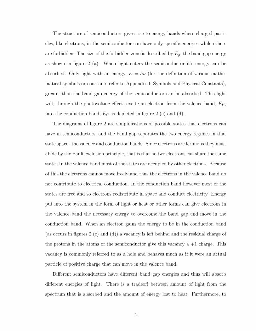
The structure of semiconductors gives rise to energy bands where charged parti-
cles, like electrons, in the semiconductor can have only specific energies while others
are forbidden. The size of the forbidden zone is described by Eg, the band gap energy
as shown in figure 2 (a). When light enters the semiconductor it’s energy can be
absorbed. Only light with an energy, E = h⌫ (for the definition of various mathe-
matical symbols or constants refer to Appendix I: Symbols and Physical Constants),
greater than the band gap energy of the semiconductor can be absorbed. This light
will, through the photovoltaic e↵ect, excite an electron from the valence band, EV ,
into the conduction band, EC as depicted in figure 2 (c) and (d).
The diagrams of figure 2 are simplifications of possible states that electrons can
have in semiconductors, and the band gap separates the two energy regimes in that
state space: the valence and conduction bands. Since electrons are fermions they must
abide by the Pauli exclusion principle, that is that no two electrons can share the same
state. In the valence band most of the states are occupied by other electrons. Because
of this the electrons cannot move freely and thus the electrons in the valence band do
not contribute to electrical conduction. In the conduction band however most of the
states are free and so electrons redistribute in space and conduct electricity. Energy
put into the system in the form of light or heat or other forms can give electrons in
the valence band the necessary energy to overcome the band gap and move in the
conduction band. When an electron gains the energy to be in the conduction band
(as occurs in figures 2 (c) and (d)) a vacancy is left behind and the residual charge of
the protons in the atoms of the semiconductor give this vacancy a +1 charge. This
vacancy is commonly referred to as a hole and behaves much as if it were an actual
particle of positive charge that can move in the valence band.
Di↵erent semiconductors have di↵erent band gap energies and thus will absorb
di↵erent energies of light. There is a tradeo↵ between amount of light from the
spectrum that is absorbed and the amount of energy lost to heat. Furthermore, to
4
E
x
EC
EV
mostly empty states
mostly filled states
Forbidden Energies Eg
(a) Electronic Structure of Semiconduc-tors
E
x
EC
EVh⌫
(b) h⌫ < Eg, No light absorption. Semi-conductor is transparent to light of thisenergy
E
x
EC
EV
h⌫
(c) h⌫ = Eg, Light is absorbed withthe energy equal to the band gap (directsemiconductors)
E
x
EC
EV
h⌫
�E
(d) h⌫ > Eg, Light is absorbed and excessenergy, �E, is lost to heat
Figure 2: (a) Depiction of the conduction band, valence band, and band gap energyin a semiconductor (EC , EV , and Eg respectively). (b) - (d) Absorption of light ofvarious energies in a semiconductor.
collect power solar cells work on the principle of the pn junction.
1.2.2 Doping, PN Junctions, and Recombinations
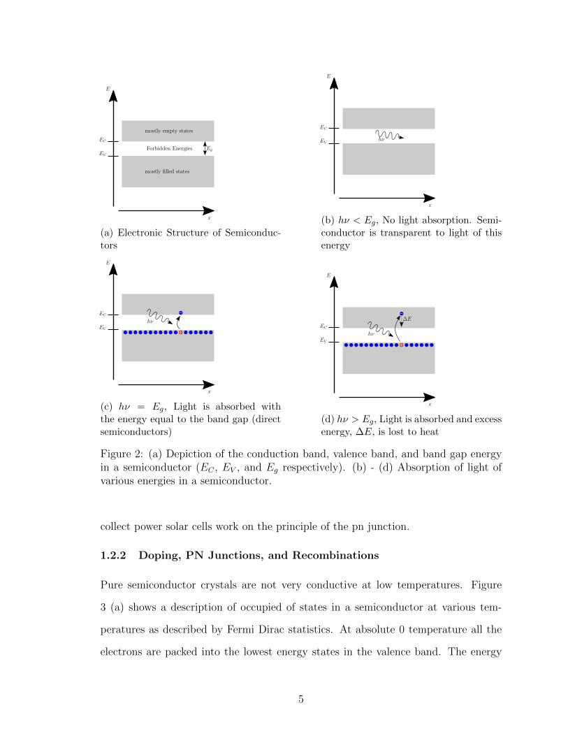
Pure semiconductor crystals are not very conductive at low temperatures. Figure
3 (a) shows a description of occupied of states in a semiconductor at various tem-
peratures as described by Fermi Dirac statistics. At absolute 0 temperature all the
electrons are packed into the lowest energy states in the valence band. The energy
5
%Occup
ation
EEFEV
1
EC
Cold
Hot
(a) Occupation of states around the fermilevel
x
EF
EV
EC
E
(b) An intrinsic semiconductor with fermilevel indicated
x
EFE
V
EC
E
EF
ED
EA
(c) n-type and p-type doped semiconduc-tors with example electrons and holes
x
EF
EV
EC
E
EA
ED
Depletion Regionn-type
p-typeqV
�xn0
xp00
(d) an np junction in a semiconductorwith energies indicated
Figure 3: Occupation of states at di↵erent temperatures in a semiconductor as wellas a description of doping and the formation of an np junction
level that all of the electrons are under at 0 K is called the fermi level, EF . As
the semiconductor is heated more and more electrons have the energy to occupy the
conduction band. Often, especially with wide band gap semiconductors, at room
temperature the semiconductors are still not very conductive. Thus it is common to
intentionally add impurities, called dopants, to increase the amount of carriers in the
semiconductor. These impurities have a di↵erent number of outer shell electrons than
the semiconductor material, that is they are not isoelectronic to the semiconductor
material. The dopants also perturb the crystal lattice of the semiconductor and create
additional energy levels within the band gap as depicted in figure 3 (c). If the energy
of the dopant is close to the conduction band and the dopant has more electrons than
6
the intrinsic semiconductor it is called a donor because it will readily “donate” its
electrons to the conduction band. Whereas if the dopant energy is close valence band
and it has fewer electrons than the semiconductor it is called an acceptor. Ideally
the energies involved are low enough that at room temperature most of the donors
have lost their electrons and most of the acceptors have gained extra electrons thus
resulting in a higher than normal amount of electrons in the conduction band and
holes in the valence band. Examples of donors and acceptors in silicon include phos-
phorus (donor) and boron (acceptor) [7]. When a semiconductor device is made with
a gradient of doping concentrations a junction is formed. Electrons in the conduction
band and holes in the valence band will distribute to cancel out charge of the junction
and the end result is depicted in figure 3 (d).
In an np or pn junction the fermi levels equalize and the conduction and valence
bands bend. The amount that the valence and conduction bands bend is called the
built-in potential, qV . This can be calculated from the concentration of donors, ND,
acceptors, NA, as well as the intrinsic carrier concentration for this semiconductor at
room temperature, ni (assuming all donors and acceptors are ionized) by the following
equation [7]:
V =kT
qln
✓NAND
n2
i
◆(1)
All constants can be found in Appendix I: Symbols and Physical Constants.
The zone where the bands are bending is called the depletion region. This zone
is between the xn0
and xp0 junction depths and has a depletion width defined as
W0
= xn0
+xp0. In the depletion region electrons and holes have recombined cancelling
each other out.
There are several ways in which electrons and holes can be generated or can
recombine to cancel each other out. Firstly holes in the valence band and electrons
in the conduction band can be generated or recombine directly with the absorption
or emission of light. This is called direct band-to-band generation or recombination
7
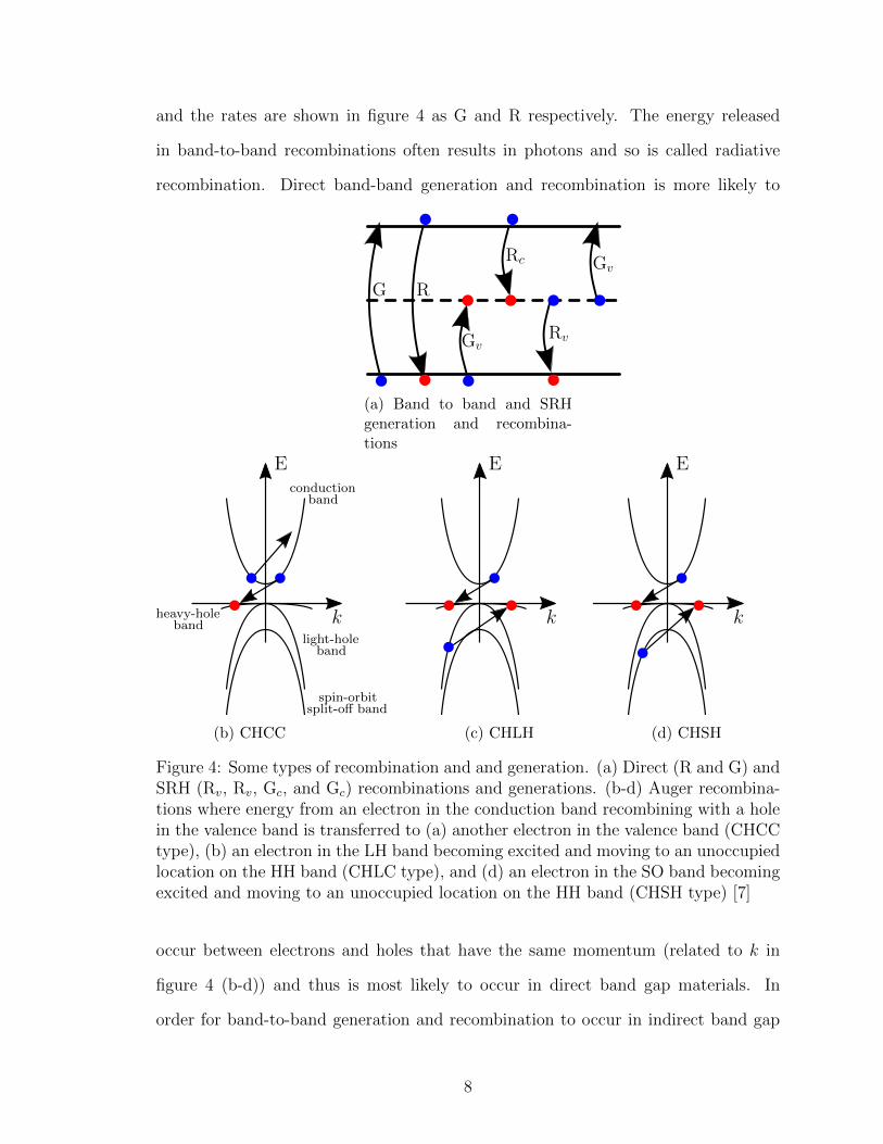
and the rates are shown in figure 4 as G and R respectively. The energy released
in band-to-band recombinations often results in photons and so is called radiative
recombination. Direct band-band generation and recombination is more likely to
G R
Gv
Rc
Rv
Gv
(a) Band to band and SRHgeneration and recombina-tions
E
k
conduction
band
heavy-hole
band
light-hole
band
spin-orbit
split-o↵ band
(b) CHCC
E
k
(c) CHLH
E
k
(d) CHSH
Figure 4: Some types of recombination and and generation. (a) Direct (R and G) andSRH (Rv, Rv, Gc, and Gc) recombinations and generations. (b-d) Auger recombina-tions where energy from an electron in the conduction band recombining with a holein the valence band is transferred to (a) another electron in the valence band (CHCCtype), (b) an electron in the LH band becoming excited and moving to an unoccupiedlocation on the HH band (CHLC type), and (d) an electron in the SO band becomingexcited and moving to an unoccupied location on the HH band (CHSH type) [7]
occur between electrons and holes that have the same momentum (related to k in
figure 4 (b-d)) and thus is most likely to occur in direct band gap materials. In
order for band-to-band generation and recombination to occur in indirect band gap
8
materials, like silicon, a third virtual particle called a phonon must also interact
with the electron and hole so that momentum is conserved. Secondly, impurities and
defects in the semiconductor crystal lattice can introduce energy levels in the band gap
called traps. Electrons can move from the valence and conduction bands into these
trap levels in a process described by Shockley Read and Hall and are thus called SRH
recombinations. The energy released from SRH recombinations are usually given to
the crystal lattice in the form of phonons, or vibrations that can dissipate as heat.
Thus band-to-trap recombinations are generally non-radiative. The other major type
of recombination is Auger recombination. This occurs when the energy released by the
recombination of the electron and hole is transferred to a third particle. This occurs
most often in direct band gap semiconductors with a small band gap at elevated
temperatures. The three possible Auger recombination mechanisms are shown in
figure 4 (b-d).
Knowledge of band gap energies, pn junctions, recombinations, and defects is
essential to the design of successful solar cells. In the next section we’ll investigate
how this information is employed to define the solar cell e�ciency as well as the use
of InGaN as a material for solar cells, the challenges associated with using InGaN,
and progress made in the scientific community towards e�cient InGaN based solar
cells.
1.3 Solar Cells
An understanding of the solar spectrum and semiconductor physics that govern the
absorption and collection of solar energy are essential to the development of solar
cells. However, photovoltaics is not a new subject and there are many competing
technologies both in the laboratory and commercial markets. An overview of these
technologies is presented to provide context for InGaN solar cells and to show the
pressures driving innovation in solar cells. Furthermore by investigating the solutions
9
to problems faced by other solar cell technologies we can adapt the technology and
gain inspiration for InGaN solar cells.
1.3.1 The Economics of Solar Power
The energy sector is an extremely competitive area of the economy. The total cost
of solar cells must be understood in order to determine how much a it costs to make
electricity can be produced. This figure of merit can be analyzed in many ways:
levelized cost of electricity, energy payback time, etc.. Fundamentally these equations
have two parts. First, how much does electricity cost, and second how much electricity
is made by the solar cell per dollar. The amount of electricity made by a certain
solar cell depends on the type of cell used. The national renewable energy laboratory
(NREL) in the United States benchmarks various solar cell technologies and maintains
a database of solar cell performance for a number of types of solar cells. As time passes
there are more and more materials designs used to make solar cells and the conversion
e�ciency of each design increases. Many of these materials and designs, and their
limitations are the subject of the subsequent sections of this chapter. However, before
discussion of the di↵erences between Si and CdTe solar cells we should fill in the
remaining pieces of the economic equation: the cost of solar cells and a comparison
of the cost of electricity produced by solar power and other sources like nuclear and
coal.
The costs of solar power are often broken into three components: the cost of the
solar cell module, the cost of the inverter, and “balance of systems” (BOS) costs which
cover everything else from the wiring to the frames and the solar trackers used in CPV
systems. The module cost depends on the type of solar cell that is used (Si, CIGS,
flat panel, concentrated, etc.). For example for an unconcentrated solar module set
on an incline in southern Europe the largest factor in the cost of a crystalline Si solar
cell module is the production of the crystalline Si itself, while for a CIGS cell, which
10
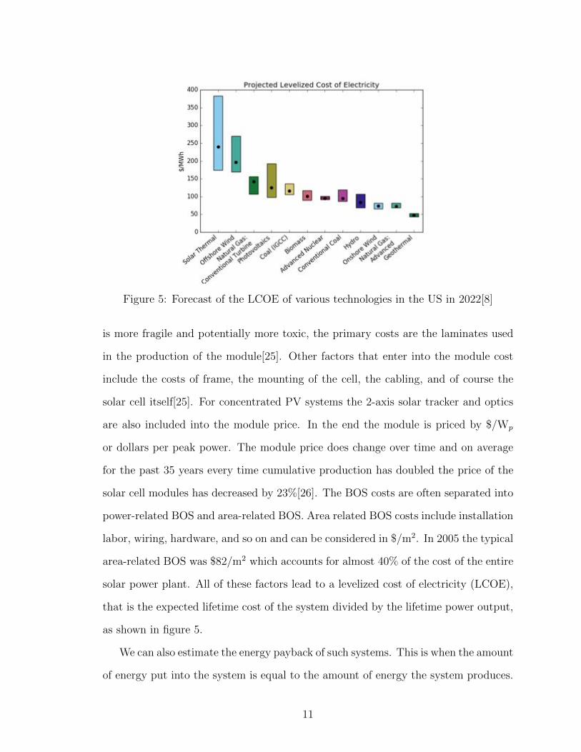
Figure 5: Forecast of the LCOE of various technologies in the US in 2022[8]
is more fragile and potentially more toxic, the primary costs are the laminates used
in the production of the module[25]. Other factors that enter into the module cost
include the costs of frame, the mounting of the cell, the cabling, and of course the
solar cell itself[25]. For concentrated PV systems the 2-axis solar tracker and optics
are also included into the module price. In the end the module is priced by $/Wp
or dollars per peak power. The module price does change over time and on average
for the past 35 years every time cumulative production has doubled the price of the
solar cell modules has decreased by 23%[26]. The BOS costs are often separated into
power-related BOS and area-related BOS. Area related BOS costs include installation
labor, wiring, hardware, and so on and can be considered in $/m2. In 2005 the typical
area-related BOS was $82/m2 which accounts for almost 40% of the cost of the entire
solar power plant. All of these factors lead to a levelized cost of electricity (LCOE),
that is the expected lifetime cost of the system divided by the lifetime power output,
as shown in figure 5.
We can also estimate the energy payback of such systems. This is when the amount
of energy put into the system is equal to the amount of energy the system produces.
11

In Germany, for example, where there are generous subsidies for renewable energy,
but the climate and latitude are not favorable for solar power the energy payback for
a solar power plant is approximately 2.5 years[26]. In Sicily where it is much sunnier
a p-Si power plant can reach it’s energy payback in 1 year. If, on average, the plant
lasts 20 years that means that the solar power plant in Sicily will produce 20⇥ more
power than was used to make it[26]. Furthermore, the operations and maintenance
costs, not to mention fuel costs, of photovoltaic systems are low compared to other
traditional methods of electricity production[27].
This being said, figure 5 makes it clear that, at least for the foreseeable future,
solar power is not a “silver bullet” solution to the issue of clean and inexpensive
electricity. Instead terrestrial solar power will be one of many solutions deployed to
provide electricity to an area depending on its location, and climate. However, as in
most economic topics, unforeseeable events, like changes to the price of coal or oil or
public policy on global warming, as well as technological advancements will surely tip
the economic balance towards or away from solar power. Thus a diverse application
of energy technologies is employed including solar, wind, and biomass power, as well
as more traditional methods like coal and natural gas.
1.3.2 Single Junction Solar Cells
Historically Si has been the primary choice for single junction solar cells[22, 26]. Si
has many qualities that lend itself to use as a solar cell. Firstly it is chemically
abundant, and secondly it has a band gap energy of 1.12 eV which is close to the
optimal band gap for a single junction solar cell[28]. Furthermore the use of Si in
other areas of microelectronics has led to the development of processing standards
and driven down the cost of fabricating Si based devices further further encourag-
ing it’s use in photovoltaics. In fact according to the Fraunhofer institute Si based
photovoltaics accounted for 93% of total solar cell production in 2015[26]. Other
12
thin film technologies like CdS or CdTe rely on the fact that very little material is
necessary for producing a solar cell, further driving down costs. At the lowest end of
the cost-spectrum lie emerging PV technologies like organic solar cells and perovskite
materials. Each of these avenues for a↵ordable, terrestrial photovoltaics remains an
active area of research and each one has its own benefits as well as its challenges.
1.3.2.1 Crystalline Silicon Solar Cells
Monocrystalline Si solar cells are the most expensive to manufacture because they
require slow and careful manufacturing to produce[24]. To begin the cells are typically
formed using the Czochralski growth method in which a melt of liquid Si is maintained
with a single-crystal seed dipped into the melt[29]. The seed is rotated so as to
maintain uniformity and slowly drawn from the melt. The seed acts as a template for
crystal growth and the Si forms as the crystal cools as a result of being drawn from
the melt. The rate at which the seed is drawn from the melt will result in di↵erent
diameters of crystal ingots being formed[29]. The resulting ingots are then polished
to a uniform diameter and cut to form wafers. It is not uncommon to use the float
zone method to produce monocrystalline Si wafers also[30].
The typical fabrication process then utilize anisotropic etching to pattern the sur-
face in an inverted pyramidal structure as described by Campbell and Green[31].
This increases the optical thickness of the solar cell by promoting internal light
reflections[31, 32]. The top surface is then doped using dopant di↵usion or ion
implantation[32]. The front side of the structure is passivated using dielectrics like
atomic layer deposition (ALD) formed Al2
O3
and SiNx[32, 30]. These dielectrics
serve the dual purposes of reducing locations for surface recombinations as well as
forming an anti-reflective coating. This high-quality electrical passivation lowering
the surface recombination is what is known as a “passivated emitter” configuration.
Photolithography and chemical etching can be used to open the dielectric to place
13
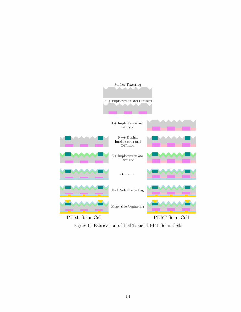
Surface Texturing
P++ Implantation and Di↵usion
N++ DopingImplantation and
Di↵usion
N+ Implantation andDi↵usion
Oxidation
Back Side Contacting
Front Side Contacting
P+ Implantation andDi↵usion
PERL Solar Cell PERT Solar Cell
Figure 6: Fabrication of PERL and PERT Solar Cells
14
the top contact grid. Screen printed contacts are the cheapest, but come at a cost to
the e�ciency of the solar cell due to shadowing e↵ects[30]. Buried contact based on
laser grooved structures have been shown to improve the e�ciency of the solar cells,
but add complexity to the process[33, 34, 24]. It is typically to utilize electroplated
surface contacts as a compromise between the losses of screen printed contacts and
the buried contact design[30]. Attention must be paid to the bottom of the solar cell
as well. Depending on the resistivity of the solar cell either a totally di↵used or locally
di↵used design is preferred. In higher resistivity cells the totally di↵used design is
favored where a light dopant concentration is formed across the entire bottom of the
cell to prevent current crowding around the higher doped areas near the contacts[30].
In the locally di↵used design a “PassDop” process is preferred where the dielectric
passivation is opened on the back side of the solar cell and dopants allowed to di↵use
through the openings[32]. In both configurations the rear metal contact is formed
on the entire back surface. This creates a mirror to increase the optical path for
any light that either wasn’t absorbed by the solar cell or light that has been emitted
from radiative cooling. The contact also completes the electrical circuit at the points
where the cell is highly doped and the oxide is open. Schematics of the fabrication of
the passivated emitter, rear local di↵usion (PERL) and passivated emitter, rear total
di↵usion (PERT) solar cell designs are shown in figure 6.
1.3.2.2 Polycrystalline Silicon Solar Cells
The processes for manufacturing multicrystalline or polycrystalline Si solar cells re-
quire less stringent tolerances than those used to make monocrystalline Si, and are
therefore cheaper[24]. Like monocrystalline Si, polycrystalline Si is also grown from a
melt, however the material is allowed to solidify without the presence of a seed crystal
resulting in the polycrystalline structure. Typically the crucible containing molten Si
is allowed to cool slowly from the bottom resulting in a slab of polycrystalline Si which
15
is later cut into bricks and sliced into wafers. The primary issue with polycrystalline
Si solar cells is that they have poorer current-voltage characteristics as defined by the
dark current and open circuit voltage[22, 35]. These e↵ect arise from band bending
at the grain boundaries due to strained crystal bonds. In addition dangling crystal
bonds at the boundaries result manifest as both a short circuit path reducing the
shunt resistance as well as a recombination center. This adversely e↵ects the power
extracted from the solar cell. In order to avoid recombination losses at the grain
boundaries relatively large (⇡ 1 mm2) polysilicon grains are preferred[35]. Despite
these challenges to e�ciency with respect to monocrystalline silicon, the reduction in
cost and the long lifetime of polycrystalline solar cells have resulted in polycrystalline
solar cells accounting for 68% of total photovoltaic production in 2015[26].
1.3.2.3 Thin Film Solar Cells
There are large variety of materials and device designs that fall into the category
of thin film solar cells. The most prominent material systems that fall into this
category are amorphous silicon, cadmium telluride (CdTe), copper indium gallium
selenide (CIGS), and gallium arsenide (GaAs). These technologies have some attrac-
tive qualities, like their potential for high e�ciencies, flexibility allowing for so called
roll-to-roll processing, but they also have their drawbacks and according to the annual
report on photovoltaics published by the Fraunhofer Institute thin-film technologies
accounted for 8% of total photovoltaic production in 2015[26].
Amorphous Silicon
Amorphous silicon (a-Si) can, in principle, be made more cost e↵ectively than poly-
crystalline silicon[24]. This comes at a cost of solar cell e�ciency, however. The
lack of long-range structure results in a high defect density inserting traps within the
energy band gap of the material. These traps make the formation of a pn junction
16
in amorphous silicon an impossibility. Furthermore the traps prevent current flow re-
sulting in poor electrical performance of the solar cells[24]. The addition of hydrogen
into the a-Si can saturate the traps and lead to an increase of electrical performance.
The addition of hydrogen also leads to an increase of the band gap energy from 1.1
eV to 1.7 eV[36, 37]. However there is a degradation of the a-Si that occurs under
long-term exposure to light. This Staebler-Wronski e↵ect is caused by energetic light
creating dangling bonds within the material that act as recombination centers[38].
This means that the lifetime of the cell is shorter than those made of polycrystalline
and monocrystalline Si[36, 37]. of Unlike mono- and polycrystalline silicon a-Si is
deposited as a very thin film meaning that it uses very little material to create a solar
cell. This is an advantage due to the high cost of monocrystalline si ingots [26]. With
these advances a-Si has advanced to having a 14% e�ciency[39].
Cadmium Telluride
Cadmium Telluride (CdTe) Cells are actually a heterojunction solar cell based on
stacking n-type cadmium sulfide (CdS) and p-type CdTe. The resulting structure has
a band gap energy of 1.5 eV which is very close to the ideal band gap of 1.3 eV required
for maximum power extraction from the solar spectrum with a single junction. In
fact the CdTe solar cells have been reported to have a 22.1% e�ciency[39]. One of the
factors limiting CdTe solar cells is the availability and toxcicity of the raw materials,
namely cadmium and tellurium. Both Cd and Te are toxic and Cd is classified as a
hazardous substance and thus requires special handling. Cd is generally obtained as a
waste by product from the mining and refining of Zn, and therefore can be purchased
relatively cheaply from mining companies who would otherwise store it and dispose
of it as hazardous waste. Tellurium, on the other hand, is a rare metalloid occurring
on earth in about the same abundance as platinum. Our supply of Te comes almost
exclusively as a by-product of copper refining. While new supplies have been found
17
in China, Mexico, and Sweden as well as on undersea ridges CdTe photovoltaics
currently use a large percentage of the worlds production of Te. In 2007 the United
States Geological Survey estimated global Te production in 2007 to be 135 metric
tons[40]. To produce enough CdTe solar cells to obtain 1 gigawatt of power would
require 93 metric tons of Te[41]. For reference the United States used approximately
4000 TWh of electricity in 2012, and so a 1 GW CdTe plant would be able to power
the US for 9 milliseconds and yet would use 70% of the worlds yearly Te supply to
manufacture[41]. Fortunately there are proposals to mine end-of-life CdTe modules
to recycle the Te that would allow CdTe solar cell production independent of the
mining of Te by 2038[42].
Even with the high cost of tellurium the overall cost of a CdTe solar cell is low.
Depending on the design of the CdTe module and whether materials can be purchased
at a bulk cost the cost of CdTe modules is estimated to be less than $10 USD/m2
which is very competitive compared with monocrystalline Si[43, 44].
Copper Indium Gallium Selenide
Copper indium gallium selenide (CIGS) is a solid solution of the semiconductors
copper indium selenide (CIS) and copper gallium selenide (CGS) and so can be rep-
resented with the chemical formula CuInxGa1�xSe
2
. By varying the relative concen-
trations of In and Ga the band gap energy can be tuned from 1 eV to 1.7 eV, making
it an interesting candidate for high e�ciency single junction photovoltaics. To date
the best CIGS solar cell has an e�ciency of 22.6%.
CIGS solar cells are formed from the bottom up. First, the back contact, typically
molybdenum, is sputtered onto a substrate, typically glass[45]. The surface morphol-
ogy and adhesion of the contact to the glass are important for the following CIGS
deposition. The CIGS deposition typically is either done using a technique like co-
evaporation where the Se is introduced gradually throughout the entire process or in a
18
multistep process where first the metal layers are deposited followed by chalgenation
using either H2
Se gas or elemental Se [45]. Following the CIGS absorber layer depo-
sition there is a bu↵er layer, often CdS, deposited followed by the top contacts[45].
The top contacts are normally some combination of transparent conductors (ZnO or
ITO) and metal grids of Al or Ni/Al. Finally, antireflection coatings of materials
like MgF2
are added to complete the structure[45]. Of the two methods of absorber
region formation mentioned the best results come from the single step process using
co-evaporation[46, 45].
The co-evaporation technique is a multistage process in which the metal fluxes,
temperature, and metal:Se ratio are controlled to obtain the appropriate film. Of-
ten this method is performed in a molecular beam epitaxy system (MBE)[45]. The
metal sources are evaporated from e↵usion cells in the presence of H2
Se gas. First a
layer of InGaSe is formed at a relatively low temperature (300-350� C). Then Cu is
deposited at an elevated temperature which will mix with the InGaSe layer to form
a uniform, Cu-rich CIGS layer. The Cu supply is then cut o↵ and the amount of In
and Ga increased to form the top layer. The top layer is Cu-deficient and forms an
ordered vacancy compound (OVC) at the surface that is very beneficial for solar cell
performance[46, 45].
The co-evaporation technique produces the highest quality absorber region, but is
slower than the metal deposition-selenization process[45]. In these methods the metal
precursors are deposited in stacks either by sputtering, evaporation, or electrochemical
deposition. These process are faster, can be scaled up for higher throughput, and
occur at a lower temperature than co-evaporation and are therefore more economical.
Chalcogenation then occurs at approximately 400� C[45]. The formation rates of CIS
and CGS are not the same and as a result the films may not be homogeneously mixed
and may separated CGS and CIS phases that degraded performance. However, like
most processes for photovoltaics the degradation in performance must be weighed
19
against cost savings and in this case the cost savings lead to economically viable solar
cells.
Gallium Arsenide
Gallium arsenide, like GaN is a III-V semiconductor, and also like GaN it is most
frequently grown by MOCVD. For solar cell production an epitaxial lift-o↵ technique
pioneered by Konagai et al. is preferred because the GaAs template may be reused
for future MOCVD growths cutting costs[47]. In this process an AlAs sacrificial layer
is grown followed by the GaAs/InGaAsP active regions[47, 11]. Alta Devices has
developed a process in which the back contact is then formed on the surface of the
substrate[10]. This back contact often acts as a mirror to promote photon absorption.
A backing material is then bonded to the back contact and the AlAs is selectively
wet etched in hydrofluoric acid[10, 11]. The resulting cell can then be flipped and the
front contact layer and antireflective layers formed[11].
Of all the solar cells discussed so far, GaAs cells show the highest performance
of between 27 and 28% e�ciency. These cells are also the most costly due to the
energy intensive MOCVD techniques used to make them. Also the cells are fragile
and there is a decrease in the yield due to failures during processing. As such GaAs
solar cells are rarely used as a single junction solar cell, especially for unconcentrated
photovoltaics. Instead GaAs is more frequently used a component of multijunction
solar cells used in concentrated photovoltaics or space applications.
1.3.2.4 Emerging Solar Cells (Organic, Perovskite, etc)
Emerging solar cell technologies are those technologies that have yet to make it to
mass production, but have the potential to impact solar energy production in the
future. Three technologies in particular are heavily researched and those are organic
solar cells, dye sensitized solar cells, and perovskite solar cells. Schematics of these
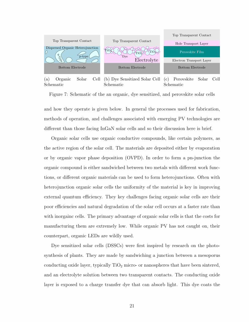
devices are shown in figure 7. A brief outline of how these solar cells are formed
20
Top Transparent Contact
Dispersed Organic Heterojunction
Bottom Electrode
n-type
p-type
(a) Organic Solar CellSchematic
Bottom Electrode
TiO2 TiO
2TiO2
Dye
Electrolyte
Top Transparent Contact
(b) Dye Sensitized Solar CellSchematic
Bottom Electrode
Electron Transport Layer
Perovskite Film
Hole Transport Layer
Top Transparent Contact
(c) Perovskite Solar CellSchematic
Figure 7: Schematic of the an organic, dye sensitized, and perovskite solar cells
and how they operate is given below. In general the processes used for fabrication,
methods of operation, and challenges associated with emerging PV technologies are
di↵erent than those facing InGaN solar cells and so their discussion here is brief.
Organic solar cells use organic conductive compounds, like certain polymers, as
the active region of the solar cell. The materials are deposited either by evaporation
or by organic vapor phase deposition (OVPD). In order to form a pn-junction the
organic compound is either sandwiched between two metals with di↵erent work func-
tions, or di↵erent organic materials can be used to form heterojunctions. Often with
heterojunction organic solar cells the uniformity of the material is key in improving
external quantum e�ciency. They key challenges facing organic solar cells are their
poor e�ciencies and natural degradation of the solar cell occurs at a faster rate than
with inorgainc cells. The primary advantage of organic solar cells is that the costs for
manufacturing them are extremely low. While organic PV has not caught on, their
counterpart, organic LEDs are wildly used.
Dye sensitized solar cells (DSSCs) were first inspired by research on the photo-
synthesis of plants. They are made by sandwiching a junction between a mesoporus
conducting oxide layer, typically TiO2
micro- or nanospheres that have been sintered,
and an electrolyte solution between two transparent contacts. The conducting oxide
layer is exposed to a charge transfer dye that can absorb light. This dye coats the
21
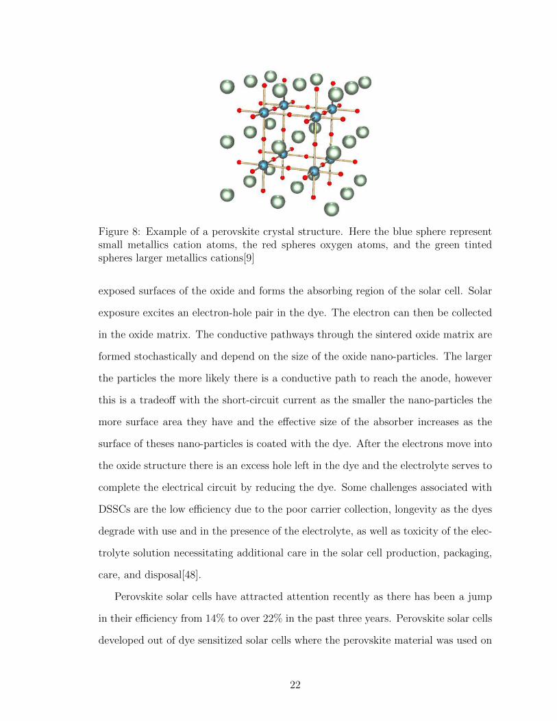
Figure 8: Example of a perovskite crystal structure. Here the blue sphere representsmall metallics cation atoms, the red spheres oxygen atoms, and the green tintedspheres larger metallics cations[9]
exposed surfaces of the oxide and forms the absorbing region of the solar cell. Solar
exposure excites an electron-hole pair in the dye. The electron can then be collected
in the oxide matrix. The conductive pathways through the sintered oxide matrix are
formed stochastically and depend on the size of the oxide nano-particles. The larger
the particles the more likely there is a conductive path to reach the anode, however
this is a tradeo↵ with the short-circuit current as the smaller the nano-particles the
more surface area they have and the e↵ective size of the absorber increases as the
surface of theses nano-particles is coated with the dye. After the electrons move into
the oxide structure there is an excess hole left in the dye and the electrolyte serves to
complete the electrical circuit by reducing the dye. Some challenges associated with
DSSCs are the low e�ciency due to the poor carrier collection, longevity as the dyes
degrade with use and in the presence of the electrolyte, as well as toxicity of the elec-
trolyte solution necessitating additional care in the solar cell production, packaging,
care, and disposal[48].
Perovskite solar cells have attracted attention recently as there has been a jump
in their e�ciency from 14% to over 22% in the past three years. Perovskite solar cells
developed out of dye sensitized solar cells where the perovskite material was used on
22
top of a mesoporous TiO2
layer[49]. Later it was determined that the mesoporous
layer that is critical to DSSCs was not required opening the avenue for research into
what is now perovskite solar cells[50]. Perovskite is a solution-processable semicon-
ductor material, which means that the constituents of the film can be dissolved into
a liquid or vapor solution, transported to a substrate, and then the solvent can be
removed to form the perovskite film. A perovskite is any film that has an ABX3
structure like CH3
NH3
PbX3
, where X can be a halogen such as I, Br, or Cl. This
structure is a cubic crystal as shown in figure 8. The film can be formed by spin
coating the dissolved components onto a substrate, typically an electron transport
layer like ZnO, followed by removing the solvent by either annealing or exposure to a
diethyl ether solvent that will selectively remove the first solvent and leave the per-
ovskite film behind. Following the perovskite film formation a hole transport layer
like copper iodide is deposited by evaporation. Finally the top contact is made by
using metal or a conducting glass like ITO. The simplicity and low cost of the fabrica-
tion of perovskite solar cells, and the relatively high e�ciencies (up to 22.1% in 2016)
makes it attractive for next-generation photovoltaics. However there is a continued
problem of the film stability. Exposure to sun light and oxygen tend to degrade the
perovskite materials so the cells are very short lived.
1.3.3 Constraints on Solar Cell E�ciency, The Shockley Queisser Limit
Solar cell e�ciency is defined as the electrical power obtained from a device divided
by the optical power going into it: ⌘ = Pout/Pin = (I ⇥ V )/1000W. Both the current
and voltage from a solar cell depend on the band gap energy of the semiconductor,
thus there is an optimal value for this energy to maximize solar cell e�ciency. The
first formulation of the optimal bandgap energy as well as the theoretical maximum
e�ciency of a solar cell was determined by Shockley and Queisser in their 1961 paper.
In this paper the following assumptions were made: that a all light with an energy
23
greater than or equal to the band gap energy will be absorbed, each absorbed photon
results in one electron hole pair being generated, the only method of loss in the solar
cell is via radiative recombination, and that the cell behaves like an ideal diode and
thus can be modeled using the ideal diode equation. There are several more methods
of loss limiting the performance of physical solar cells including non-radiative recom-
bination (Auger recombination, trap assisted recombination, etc.), but the Shockley
and Queisser ignore them in order to find the best possible e�ciency for a certain
solar cell. This formulation is outlined below and then we extend the formulation
using experimentally measured solar spectra.
To begin, we consider that the sun is a spherical blackbody with a diameter of
1.39 million km, a distance to the earth of 149 million km, and temperature of 6000
K. This is a rather good approximation of the solar spectrum in space, but due
to scattering of the sun light in the atmosphere (o↵ of air, water vapor, and dust
primarily) the terrestrial spectrum is slightly di↵erent. Due to the curvature of the
earth, and the earth’s angle of inclination to the sun the amount of sunlight scattered
in the atmosphere changes based on location and season. It is convenient (and typical)
to use a normalized spectra for sunlight that has passed through 1.5 thicknesses of
atmosphere (called “air mass 1.5,” or simply AM1.5). This spectra has been measured
and is freely available from http://rredc.nrel.gov/solar/spectra/am1.5/. Both the
blackbody approximation and the spectral irradiance for AM1.5 are shown in figure
1.
It is convenient to convert the solar spectral irradiance (dEd�
) from figure 1 from
units of W per m2 per nm to the number of photons per m2 per nm (dNd�
).
24
Ephoton = h⌫ (2)
dN
d�=
dE/d�
Ephoton
= hc
�
=) dN
d�=
dE/d�
h⌫
=dE/d�
hc/�(3)
Where eqn. 1 is the Planck relation, and eqn. 2 converts from energy at a particular
wavelength to the number of photons of that wavelength. With dNd�
it is fairly trivial
to determine the number of photons absorbed/unit area (assuming that all photons
above the energy of the bandgap, Eg, are absorbed):
N/A =
Z hc/Eg
0
dN
d�d� (4)
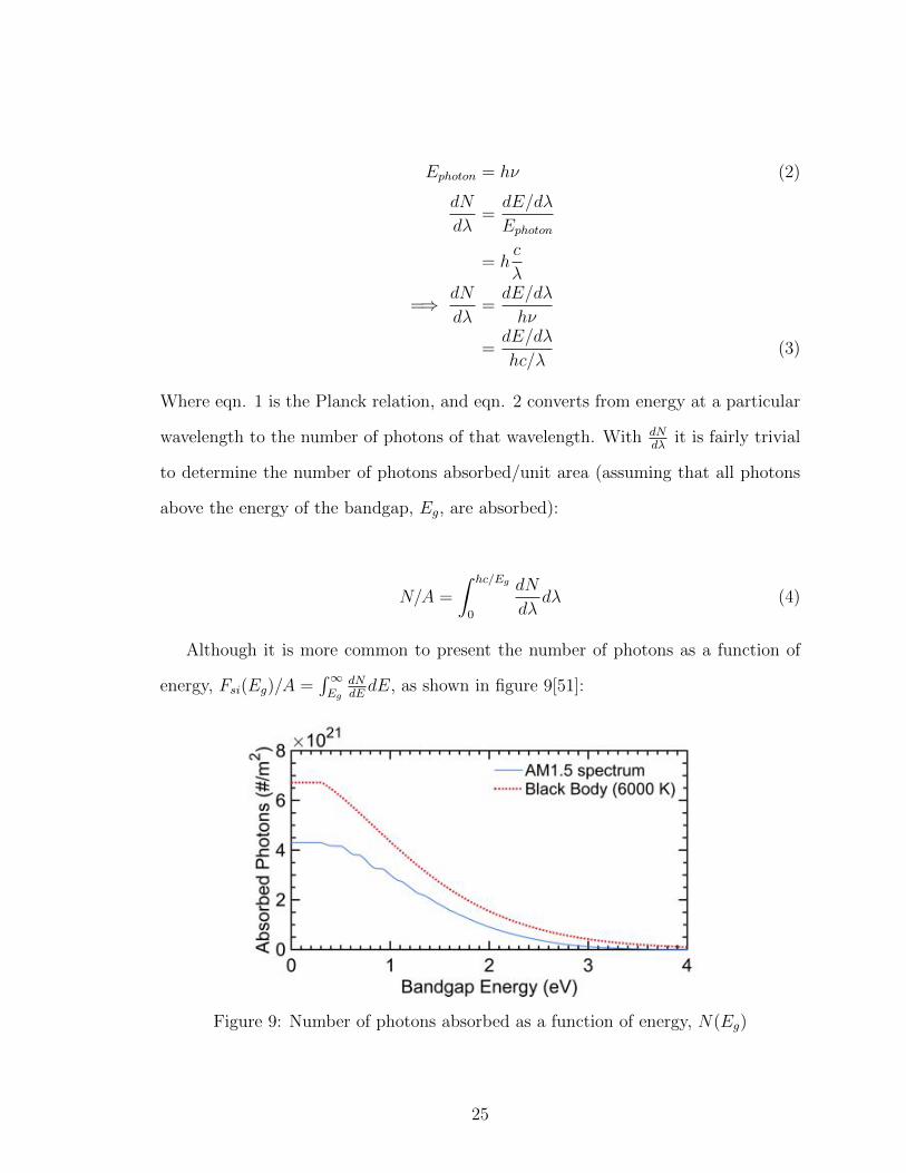
Although it is more common to present the number of photons as a function of
energy, Fsi(Eg)/A =R1E
g
dNdE
dE, as shown in figure 9[51]:
Figure 9: Number of photons absorbed as a function of energy, N(Eg)
25
To account for radiative recombination we can count the number of photons emit-
ted by the semiconductor. To do this we simply consider the material to be a black-
body that follows Planck’s distribution:
N(⌫, T ) =2⇡
c2
⌫2
exp(h⌫/kT ) � 1(5)
Where ⌫ is the frequency, c is the speed of light, k is Boltzmann’s constant, and T
is the temperature of the blackbody. We assume that for each photon emitted one
electron-hole pair is destroyed meaning the radiative recombination is given by:
F0i/A =
4⇡
c2
Z 1
Eg
/h
⌫2
exp(h⌫/kT ) � 1d⌫ (6)
Using this we can calculate the total current by subtracting the number of electrons
that recombine from those generated by illumination.
Isi = q(Fsi � F0i) (7)
From the recombination we can determine the reverse saturation current:
I0i = qF
0i (8)
Apply this value to the diode equation we obtain:
Ii(V ) = I0i(exp(qVi/kT ) � 1) � Isi (9)
= qF0i(exp(qVi/kT ) � 1) � q(Fsi � F
0i)
= qF0i exp(qVi/kT ) � qF
0i � qFsi + qF0i
= qF0i exp(qVi/kT ) � qFsi (10)
From figure 9 we can come to the conclusion that for a solar cell with a particular
band gap energy many photons may not have an energy large enough to be absorbed
and the solar cell will be transparent for these photons. This gives rise to an interesting
engineering solution: multi-junction solar cells. Solar cells can be stacked so that
26
the cells with the largest band gap are on the top. These absorb the highest energy
photons while the lower energy photons pass through the cell to be absorbed by a lower
band gap solar cell later on. We can include solar cell design into the formulation of
the Shockley-Queisser limit with no loss of generality. We do that here by considering
the maximum power point for a multi-junction solar cell with n junctions:
Pm =nX
i=1
VmiImi (11)
dPm
dV= 0
=) 0 = qd
dVi
nX
i=1
VmiF0i exp(qVmi/kT ) � VmiFsi
!(12)
If we let x = qVmi/kT , then:
0 = q/kT
kT/q
d
dx
nX
i=1
xF0i exp(x) � xFsi
!
= F0i exp(x) + xF
0i exp(x) � Fsi
= F0i exp(x) (x + 1) � Fsi
) exp(x)(x + 1) � Fsi/F0i = 0 (13)
This provides us with a system of equations to solve for each Fsi/F0i, after which we
can easily calculate the voltage where each cell is operating most e�ciently, Vmi, and
using eqns. 9 and 10 respectively we can calculate the max current and power of the
cell. The e�ciency is easily defined as:
⌘ = Pm/Pin (14)
Where Pin is the power of the light incident on the cell. This is found by integrating
the spectral irradiance over the wavelength in figure 1. Doing so using the trapezoidal
rule we find that approximately 1003 W of power fall on the earth per m2 at AM1.5.
This is unsurprising as the NREL data is normalized to 1000 W/m2. We can take
27
these results and use them to make predictions as to what the optimal band gap
energy would be for solar cells of various junctions and compare our results with
those published in the literature. The results for the short circuit current density,
open circuit voltage and theoretical maximum e�ciency as a function of band gap
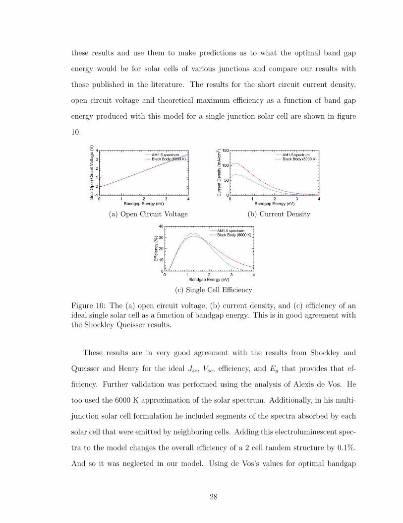
energy produced with this model for a single junction solar cell are shown in figure
10.
(a) Open Circuit Voltage (b) Current Density
(c) Single Cell E�ciency
Figure 10: The (a) open circuit voltage, (b) current density, and (c) e�ciency of anideal single solar cell as a function of bandgap energy. This is in good agreement withthe Shockley Queisser results.
These results are in very good agreement with the results from Shockley and
Queisser and Henry for the ideal Jsc, Voc, e�ciency, and Eg that provides that ef-
ficiency. Further validation was performed using the analysis of Alexis de Vos. He
too used the 6000 K approximation of the solar spectrum. Additionally, in his multi-
junction solar cell formulation he included segments of the spectra absorbed by each
solar cell that were emitted by neighboring cells. Adding this electroluminescent spec-
tra to the model changes the overall e�ciency of a 2 cell tandem structure by 0.1%.
And so it was neglected in our model. Using de Vos’s values for optimal bandgap
28
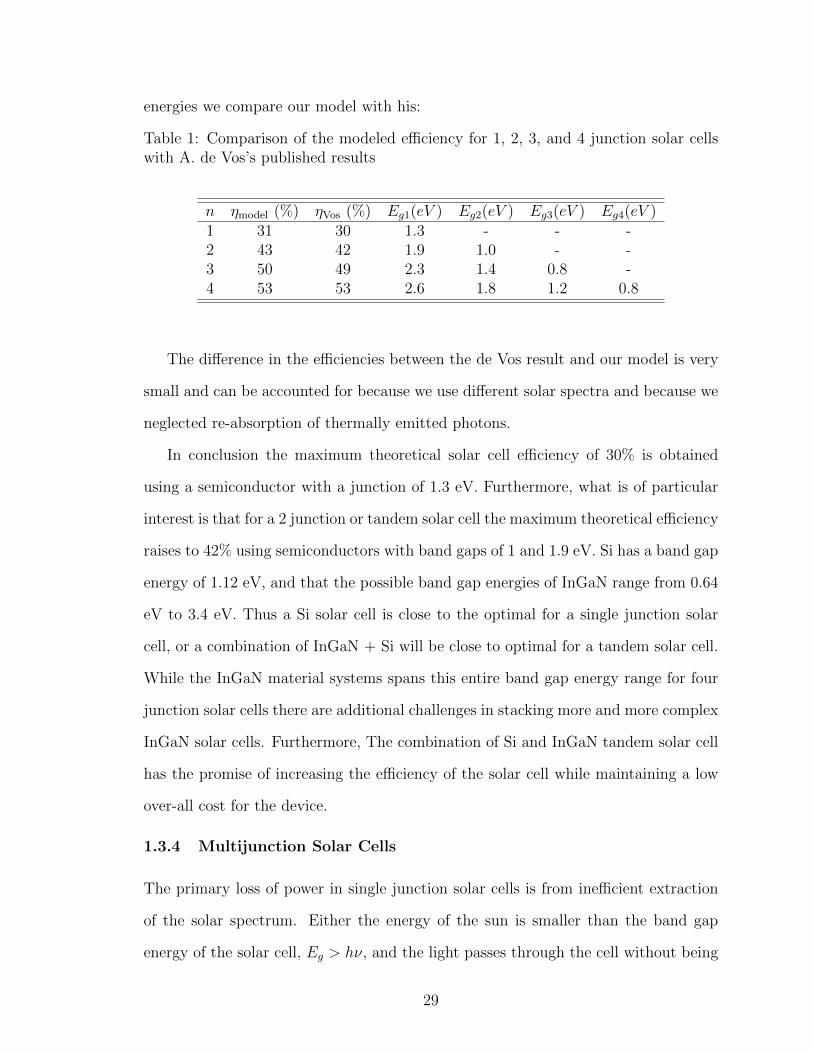
energies we compare our model with his:
Table 1: Comparison of the modeled e�ciency for 1, 2, 3, and 4 junction solar cellswith A. de Vos’s published results
n ⌘model
(%) ⌘Vos
(%) Eg1(eV ) Eg2(eV ) Eg3(eV ) Eg4(eV )1 31 30 1.3 - - -2 43 42 1.9 1.0 - -3 50 49 2.3 1.4 0.8 -4 53 53 2.6 1.8 1.2 0.8
The di↵erence in the e�ciencies between the de Vos result and our model is very
small and can be accounted for because we use di↵erent solar spectra and because we
neglected re-absorption of thermally emitted photons.
In conclusion the maximum theoretical solar cell e�ciency of 30% is obtained
using a semiconductor with a junction of 1.3 eV. Furthermore, what is of particular
interest is that for a 2 junction or tandem solar cell the maximum theoretical e�ciency
raises to 42% using semiconductors with band gaps of 1 and 1.9 eV. Si has a band gap
energy of 1.12 eV, and that the possible band gap energies of InGaN range from 0.64
eV to 3.4 eV. Thus a Si solar cell is close to the optimal for a single junction solar
cell, or a combination of InGaN + Si will be close to optimal for a tandem solar cell.
While the InGaN material systems spans this entire band gap energy range for four
junction solar cells there are additional challenges in stacking more and more complex
InGaN solar cells. Furthermore, The combination of Si and InGaN tandem solar cell
has the promise of increasing the e�ciency of the solar cell while maintaining a low
over-all cost for the device.
1.3.4 Multijunction Solar Cells
The primary loss of power in single junction solar cells is from ine�cient extraction
of the solar spectrum. Either the energy of the sun is smaller than the band gap
energy of the solar cell, Eg > h⌫, and the light passes through the cell without being
29
absorbed, or the light has an energy far above the band gap and the excess energy
is wasted as heat, Eg << h⌫. Multijunction solar cells hope to counter this loss by
utilizing more than one material with more than one band gap energy to collect the
light more e�ciently.
1.3.4.1 Solar Cells with Two Junctions
From the works like that of Shockley, Queisser, de Vos and Henry we can see that
the ideal band gap energies for solar 2 junction solar cells are 1.9 and 1.0 eV[28, 51].
Common materials for 2 junction solar cells and their maximum theoretical e�ciencies
are shown in table 2. These values have been calculated based on the a model derived
from GaAs-Ge junctions using carrier mobilities and lifetimes that were appropriate
for the date of the publication, but this report has since been updated and therefore
the maximum attainable e�ciencies can be revised upwards in some cases. They
are included here to demonstrate the potential increase in e�ciency of two junction
solar cells[52, 1, 53]. The primary materials used for two junction solar cells remain
AlGaAs-Si and GaAs-InGaP with the world record, unconcentrated double junction
solar cell e�ciency of 31.6% currently held by Alta Devices[54]. This record was
achieved using by using an epitaxial lifto↵ technique by growing GaAs and InGaP
on AlAs[10, 11]. The result was fabricated by MOCVD in an inverted geometry so
that first the AlAs layer was grown followed by the upper InGaP layer was grown and
then the GaAs layer[10, 11]. The back-side contact was formed on the sample and
the resulting structure was then released by dissolving the AlAs in HF allowing for a
thin and flexible solar cell structure with back-side contacts[10, 11]. All that remains
for operation solar cells is the formation of the front-contact grid and addition of
anti-reflective coatings resulting the the structure seen in figure 11.
30
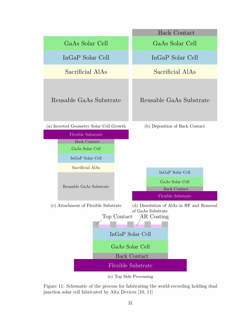
Sacrificial AlAs
Reusable GaAs Substrate
InGaP Solar Cell
GaAs Solar Cell
(a) Inverted Geometry Solar Cell Growth
Sacrificial AlAs
Reusable GaAs Substrate
InGaP Solar Cell
GaAs Solar Cell
Back Contact
(b) Deposition of Back Contact
Sacrificial AlAs
Reusable GaAs Substrate
InGaP Solar Cell
GaAs Solar Cell
Back Contact
Flexible Substrate
(c) Attachment of Flexible Substrate
InGaP Solar Cell
GaAs Solar Cell
Back Contact
Flexible Substrate
(d) Dissolution of AlAs in HF and Removalof GaAs Substrate
InGaP Solar Cell
GaAs Solar Cell
Back Contact
Flexible Substrate
Top Contact AR Coating
(e) Top Side Processing
Figure 11: Schematic of the process for fabricating the world-recording holding dualjunction solar cell fabricated by Alta Devices [10, 11]
31
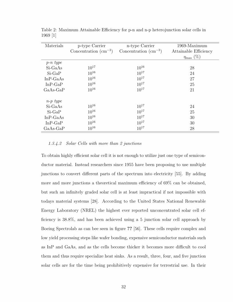
Table 2: Maximum Attainable E�ciency for p-n and n-p heterojunction solar cells in1969 [1]
Materials p-type CarrierConcentration (cm�3)
n-type CarrierConcentration (cm�3)
1969-MaximumAttainable E�ciency
⌘max
(%)p-n typeSi-GaAs 1017 1016 28Si-GaP 1016 1017 24
InP-GaAs 1016 1017 27InP-GaP 1016 1017 25
GaAs-GaP 1016 1017 21
n-p typeSi-GaAs 1016 1017 24Si-GaP 1016 1017 25
InP-GaAs 1016 1017 30InP-GaP 1016 1017 30
GaAs-GaP 1016 1017 28
1.3.4.2 Solar Cells with more than 2 junctions
To obtain highly e�cient solar cell it is not enough to utilize just one type of semicon-
ductor material. Instead researchers since 1955 have been proposing to use multiple
junctions to convert di↵erent parts of the spectrum into electricity [55]. By adding
more and more junctions a theoretical maximum e�ciency of 69% can be obtained,
but such an infinitely graded solar cell is at least impractical if not impossible with
todays material systems [28]. According to the United States National Renewable
Energy Laboratory (NREL) the highest ever reported unconcentrated solar cell ef-
ficiency is 38.8%, and has been achieved using a 5 junction solar cell approach by
Boeing Spectrolab as can bee seen in figure ?? [56]. These cells require complex and
low yield processing steps like wafer bonding, expensive semiconductor materials such
as InP and GaAs, and as the cells become thicker it becomes more di�cult to cool
them and thus require specialize heat sinks. As a result, three, four, and five junction
solar cells are for the time being prohibitively expensive for terrestrial use. In their
32
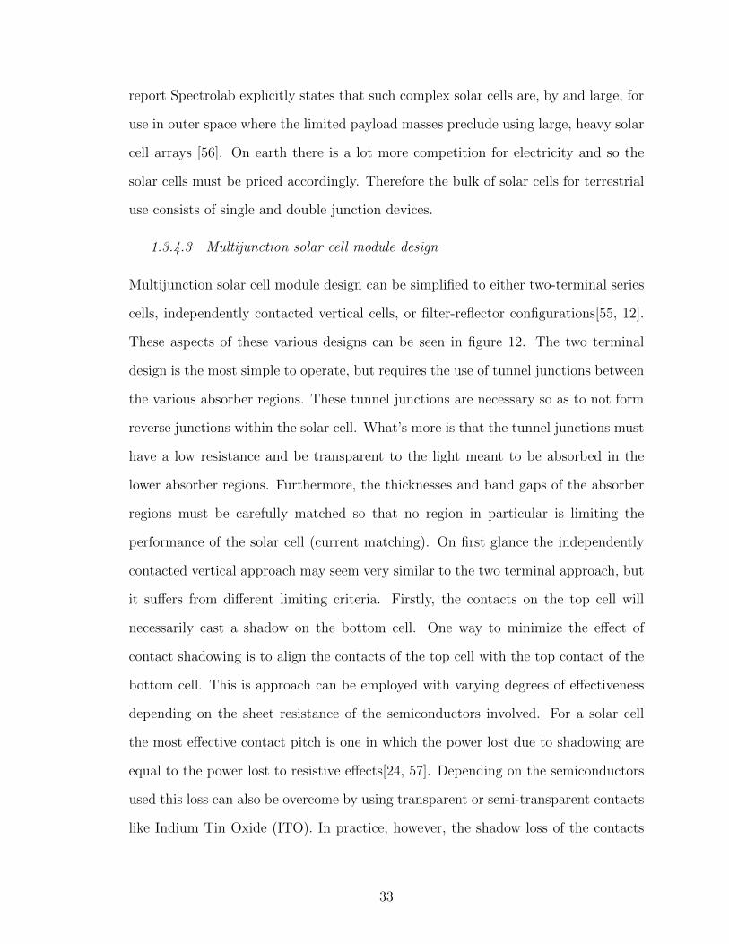
report Spectrolab explicitly states that such complex solar cells are, by and large, for
use in outer space where the limited payload masses preclude using large, heavy solar
cell arrays [56]. On earth there is a lot more competition for electricity and so the
solar cells must be priced accordingly. Therefore the bulk of solar cells for terrestrial
use consists of single and double junction devices.
1.3.4.3 Multijunction solar cell module design
Multijunction solar cell module design can be simplified to either two-terminal series
cells, independently contacted vertical cells, or filter-reflector configurations[55, 12].
These aspects of these various designs can be seen in figure 12. The two terminal
design is the most simple to operate, but requires the use of tunnel junctions between
the various absorber regions. These tunnel junctions are necessary so as to not form
reverse junctions within the solar cell. What’s more is that the tunnel junctions must
have a low resistance and be transparent to the light meant to be absorbed in the
lower absorber regions. Furthermore, the thicknesses and band gaps of the absorber
regions must be carefully matched so that no region in particular is limiting the
performance of the solar cell (current matching). On first glance the independently
contacted vertical approach may seem very similar to the two terminal approach, but
it su↵ers from di↵erent limiting criteria. Firstly, the contacts on the top cell will
necessarily cast a shadow on the bottom cell. One way to minimize the e↵ect of
contact shadowing is to align the contacts of the top cell with the top contact of the
bottom cell. This is approach can be employed with varying degrees of e↵ectiveness
depending on the sheet resistance of the semiconductors involved. For a solar cell
the most e↵ective contact pitch is one in which the power lost due to shadowing are
equal to the power lost to resistive e↵ects[24, 57]. Depending on the semiconductors
used this loss can also be overcome by using transparent or semi-transparent contacts
like Indium Tin Oxide (ITO). In practice, however, the shadow loss of the contacts
33
Concentrator Lens
Secondary Concentrator Lens
Large Band Gap Solar Cell
Sm
allB
and
Gap
Sol
arC
ell
Dichroic Mirror
Figure 12: High E�ciency Solar Cell Module Design[12]
if often overlooked or ignored as a necessary evil and rightfully so because often they
account for only a small fraction of power lost in the solar cell[24]. A further concern
for independently contacted vertical solar cells is surface reflections from stacked solar
cells, but antireflective coatings can be e↵ective at countering this. Filter-reflector
devices are most similar to the independently contacted vertical cells in that each cell
can operate independently from the others and thus requires neither tunnel junctions
nor current matching. The di↵erence is that instead of stacking the cells vertically
optics are used to separate the light and distribute it to each junction individually [12].
The performance of this design is therefore dependent also on the the performance of
the optics. A major benefit of both the independently contacted vertical and filter-
reflector designs is that if the various junctions can be made on di↵erent dies and do
not have to be combined electrically and optically later. This allows for a flexibility
in the semiconductor used and the potential to avoid lattice mismatch in the growth
of the semiconductor.
34

1.4 Conclusions
Photovoltaics have many advantages that lend them to playing a large part in pro-
ducing renewable and environmentally sustainable energy. Firstly solar energy is the
abundance of solar energy. Everyday roughly 6000 times more power reaches the
earth surface in the form of sunlight than what is consumed by human activities.
Secondly, photovoltaics convert sunlight directly into electricity making it very sim-
ple to install with (generally) no moving parts. This means that it can be installed
in large scale, centrally by utilities or in a distributed manner on residential com-
mercial roofs. This contrast other methods of harvesting solar power which rely on
boiling water or liquefying salt to power mechanical turbines and are only suitable
for large-scale utilities.
Photovoltaics is not without it’s problems and challenges however. In 1961 Shock-
ley and Queisser formulated the thermodynamic maximum e�ciency for a solar cell
and crystalline silicon solar cells are nearing this technological limit. New cheaper
or higher performing solutions are required in order to make photovoltaics more eco-
nomical and see them implemented more widely. Researchers have taken up this
mantle and shown a variety of solutions from inexpensive organic based solar cells to
high performance multijunction cells. As of today there is no standardized solution.
However, we believe that using a combination of indium gallium nitride and Si we can
achieve a compromise between cost a performance that will fill the economic niche.
35
CHAPTER II
INDIUM GALLIUM NITRIDE: MATERIAL AND
GROWTH
2.1 Why Use Indium Gallium Nitride
Indium Gallium Nitride, or InGaN is predicted to be an excellent material for solar
cell applications. Firstly, it has a tunable band gap energy that spans from near UV
across nearly the entire visible spectrum allowing it to be utilized in highly e�cient
single or tandem cell designs. It is a direct band gap material and has a high coe�cient
of optical absorption. InGaN has a high resistance to irradiation making it it suitable
for extraterrestrial applications. InGaN has a relatively high thermal conductivity,
temperature resistance, and a high carrier mobility and drift velocity that suggest that
it will be a good match for concentrated photovoltaic systems. Lastly the calculated
band alignments of n-In0.45
Ga0.55
N/p-Si are should be conducive to low resistance
tandem solar cells.
These properties as well as the physical and electrical properties, crystal structure,
and the growth of InGaN by a variety of methods are discussed in detail in the
following sections. Lastly we will review the challenges associated with the growth
and fabrication of InGaN based solar cells as well as discuss the state of the art.
2.2 Indium Gallium Nitride
InGaN is a solid solution of GaN and InN. GaN and InN, as well as BN and AlN,
are III-Nitride semiconductors formed by creating a crystal with a group III (IUPAC
group 13) metal and nitrogen. The III-Nitride materials system has many unique
properties including the possibility of using strained and polarized layers to create
36
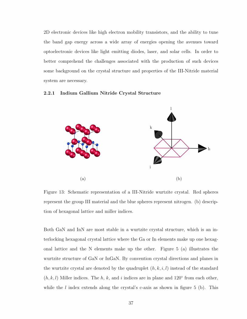
2D electronic devices like high electron mobility transistors, and the ability to tune
the band gap energy across a wide array of energies opening the avenues toward
optoelectronic devices like light emitting diodes, laser, and solar cells. In order to
better comprehend the challenges associated with the production of such devices
some background on the crystal structure and properties of the III-Nitride material
system are necessary.
2.2.1 Indium Gallium Nitride Crystal Structure
(a)
h
k
i
l
(b)
Figure 13: Schematic representation of a III-Nitride wurtzite crystal. Red spheres
represent the group III material and the blue spheres represent nitrogen. (b) descrip-
tion of hexagonal lattice and miller indices.
Both GaN and InN are most stable in a wurtzite crystal structure, which is an in-
terlocking hexagonal crystal lattice where the Ga or In elements make up one hexag-
onal lattice and the N elements make up the other. Figure 5 (a) illustrates the
wurtzite structure of GaN or InGaN. By convention crystal directions and planes in
the wurtzite crystal are denoted by the quadruplet (h, k, i, l) instead of the standard
(h, k, l) Miller indices. The h, k, and i indices are in plane and 120� from each other,
while the l index extends along the crystal’s c-axis as shown in figure 5 (b). This
37
means that the indices are not linearly independent, in fact the extra i index is can
be defined in terms of h and k: i = �(h + k). There are two lengths that define the
the equilibrium spacing of the crystal lattice and these are denoted as lengths a and
c. The crystal lattice spacing along the basal axes is a and the lattice spacing along
the vertical axis of the hexagonal prism or c-plane is c.
Furthermore, the wurtzite crystal is symmetric about the [0 0 0 1] (or c axis) direc-
tion, but lacks inversion symmetry. In other words the [0 0 0 1] and [0 0 0 1] directions
are not equivalent. The crystalline asymmetry leads to the materials being polar.
This polarization is called the spontaneous polarization, ~Psp
. Depending on how the
crystal is grown the direction of this polarization will either be Ga-faced, pointing
opposite of the growth direction as depicted in figure 5 (a), or N-faced and pointing
along the growth direction.
When stress is applied to the InGaN crystal it will deform. In the elastic regime
this deformation can be approximated by Hooke’s law. This assumes that there is
a linear relationship between the stress (pressure) and the strain (deformation), and
that this can be described by the sti↵ness of the crystal. As such Hooke’s law can be
represented using Einstein notation as: �ij = Cijkl ✏kl where �ij is the stress tensor,
Cijkl is the sti↵ness tensor and ✏kl is the deformation vector.
Deformations of the crystal will result in changes of the polarization within the
crystal, and vica versa. This phenomenon is called the piezoelectric e↵ect. The change
in piezoelectric polarization, Ppz,i, can also be related to the deformation tensor or the
stress tensor using the piezoelectric tensor, dij, by the equation: Ppz,i = dijk�jk. Thus
the total polarization can be calculated as the sum of the spontaneous polarization
resulting from the crystal lattice structure and the piezoelectric polarization resulting
from a displacement from equilibrium of the crystal lattice: ~P = ~Psp
+ ~Ppz
.
38
2.2.2 GaN and InN physical properties, and Vegard’s Law
InN and GaN each have their own properties and values for quantities like the lattice
parameters, sti↵ness and piezoelectric tensors, band gap energy, and so on. Thus
it makes sense that an alloy of the materials will result in an interpolation of these
parameters. For many of the parameters a simple linear interpolation of the param-
eters based on the composition of the alloy is accurate enough to make predictions
of the properties of the alloy as done in equation 3. In other cases a quadratic term
is added called a bowing parameter to increase the accuracy of the model and the
use of these bowing parameters is displayed in equation 4. This type of model for
physical parameters based on the relative compositions of the components is referred
to as Vegard’s Law[58, 59]. Table 3 contains a list of relevant parameters.
aIn
x
Ga
(1�x)
N
= x aInN
+ (1 � x) aGaN
(15)
aIn
x
Ga
(1�x)
N
= x aInN
+ (1 � x) aGaN
� x (1 � x) bInGaN
(16)
39
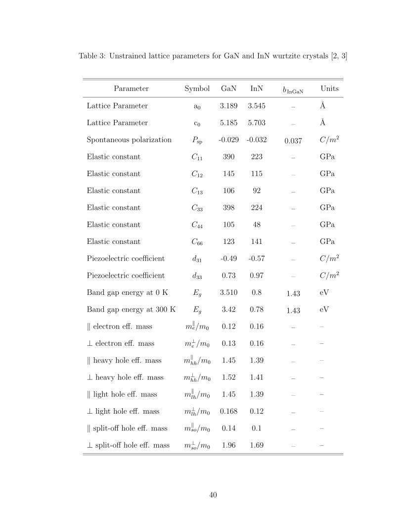
Table 3: Unstrained lattice parameters for GaN and InN wurtzite crystals [2, 3]
Parameter Symbol GaN InN bInGaN
Units
Lattice Parameter a0
3.189 3.545 – A
Lattice Parameter c0
5.185 5.703 – A
Spontaneous polarization Psp
-0.029 -0.032 0.037 C/m2
Elastic constant C11
390 223 – GPa
Elastic constant C12
145 115 – GPa
Elastic constant C13
106 92 – GPa
Elastic constant C33
398 224 – GPa
Elastic constant C44
105 48 – GPa
Elastic constant C66
123 141 – GPa
Piezoelectric coe�cient d31
-0.49 -0.57 – C/m2
Piezoelectric coe�cient d33
0.73 0.97 – C/m2
Band gap energy at 0 K Eg 3.510 0.8 1.43 eV
Band gap energy at 300 K Eg 3.42 0.78 1.43 eV
k electron e↵. mass mke/m
0
0.12 0.16 – –
? electron e↵. mass m?e /m0
0.13 0.16 – –
k heavy hole e↵. mass mkhh/m0
1.45 1.39 – –
? heavy hole e↵. mass m?hh/m0
1.52 1.41 – –
k light hole e↵. mass mklh/m0
1.45 1.39 – –
? light hole e↵. mass m?lh/m0
0.168 0.12 – –
k split-o↵ hole e↵. mass mkso/m
0
0.14 0.1 – –
? split-o↵ hole e↵. mass m?so/m0
1.96 1.69 – –
40
2.2.3 Optical Absorption of III-Nitrides
The optical properties of InGaN depend on the concentration of In. Most impor-
tantly for solar cells, is optical absorption in InGaN. The absorption of light in a
semiconductor can be modeled simply by the equation:
IT (�) = II(�)e�↵(�)t (17)
Where II and IT are the intensities of the incident and transmitted light, t is the
thickness of the material, and ↵(�) is the absorption coe�cient as a function of the
wavelength. Prior to 2002, when the band gap energy of InN was revised down to it’s
current value, the average value of ↵ was reported to be of the order of 1E5 cm�1,
and this was later confirmed[60, 61, 62, 63]. Furthermore the absorption coe�cient
was found to fit the function:
↵(hc
�) = ↵
0
qhc�� Eg
hc�
(18)
Where ↵0
is approximately 5E5 eV1/2· cm�1, h and c are Planck’s constant and the
speed of light respectively, and Eg is the band gap energy of the InGaN material
under consideration[60].
2.2.4 Strain and Polarization in III-Nitrides
Understanding of elastic deformations can be very helpful for characterizing III-
Nitride materials. As mentioned above we can relate deformation within a the crystal
to stress using Hooke’s Law. What this means is that we consider the strain to be de-
viations of atoms from their equilibrium positions within the crystal lattice as defined
by:
✏x =a
0
� a
a0
(19)
✏z =c0
� c
c0
(20)
41
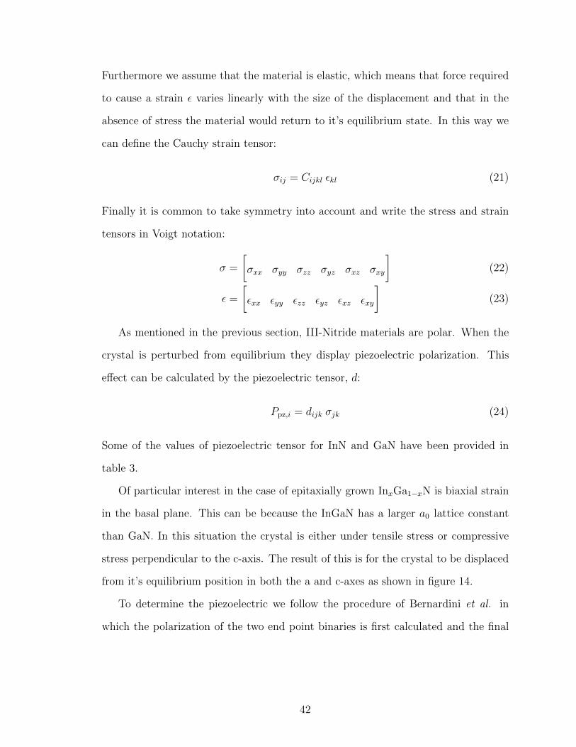
Furthermore we assume that the material is elastic, which means that force required
to cause a strain ✏ varies linearly with the size of the displacement and that in the
absence of stress the material would return to it’s equilibrium state. In this way we
can define the Cauchy strain tensor:
�ij = Cijkl ✏kl (21)
Finally it is common to take symmetry into account and write the stress and strain
tensors in Voigt notation:
� =
�xx �yy �zz �yz �xz �xy
�(22)
✏ =
✏xx ✏yy ✏zz ✏yz ✏xz ✏xy
�(23)
As mentioned in the previous section, III-Nitride materials are polar. When the
crystal is perturbed from equilibrium they display piezoelectric polarization. This
e↵ect can be calculated by the piezoelectric tensor, d:
Ppz,i = dijk �jk (24)
Some of the values of piezoelectric tensor for InN and GaN have been provided in
table 3.
Of particular interest in the case of epitaxially grown InxGa1�xN is biaxial strain
in the basal plane. This can be because the InGaN has a larger a0
lattice constant
than GaN. In this situation the crystal is either under tensile stress or compressive
stress perpendicular to the c-axis. The result of this is for the crystal to be displaced
from it’s equilibrium position in both the a and c-axes as shown in figure 14.
To determine the piezoelectric we follow the procedure of Bernardini et al. in
which the polarization of the two end point binaries is first calculated and the final
42
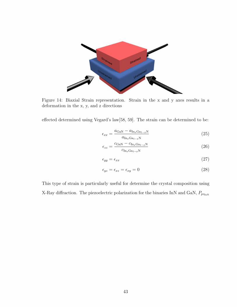
Figure 14: Biaxial Strain representation. Strain in the x and y axes results in adeformation in the x, y, and z directions
e↵ected determined using Vegard’s law[58, 59]. The strain can be determined to be:
✏xx =a
GaN
� aIn
x
Ga
1�x
N
aIn
x
Ga
1�x
N
(25)
✏zz =cGaN
� cIn
x
Ga
1�x
N
cIn
x
Ga
1�x
N
(26)
✏yy = ✏xx (27)
✏yz = ✏xz = ✏xy = 0 (28)
This type of strain is particularly useful for determine the crystal composition using
X-Ray di↵raction. The piezoelectric polarization for the binaries InN and GaN, PpzInN
43

and PpzGaN
, computed with those values of ✏:
PpzInN
=
0
BBBB@
0 0 0 0 d15
InN
0
0 0 0 d15
InN
0 0
d31
InN
d31
InN
d33
InN
0 0 0
1
CCCCA·
0
BBBBBBBBBBBBBB@
✏xx
✏xx
✏zz
0
0
0
1
CCCCCCCCCCCCCCA
(29)
PpzGaN
=
0
BBBB@
0 0 0 0 d15
GaN
0
0 0 0 d15
GaN
0 0
d31
GaN
d31
GaN
d33
GaN
0 0 0
1
CCCCA·
0
BBBBBBBBBBBBBB@
✏xx
✏xx
✏zz
0
0
0
1
CCCCCCCCCCCCCCA
(30)
Since we are interested in the c-axis direction:
PpzInN
,z = 2d31
InN
✏xx + d33
InN
✏zz (31)
PpzGaN
,z = 2d31
GaN
✏xx + d33
GaN
✏zz (32)
Introducing the Poisson ratio which can be derived from equation (6):
✏zz = �2C
13
C33
✏xx (33)
=) PpzInN
,z = 2✏xx(d31
InN
� d33
InN
C13
C33
) (34)
PpzGaN
,z = 2✏xx(d31
GaN
� d33
GaN
C13
C33
) (35)
Finally, using Vegard’s law:
Ppz,z = xPpzInN
,z + (1 � x)PpzGaN
,z (36)
44
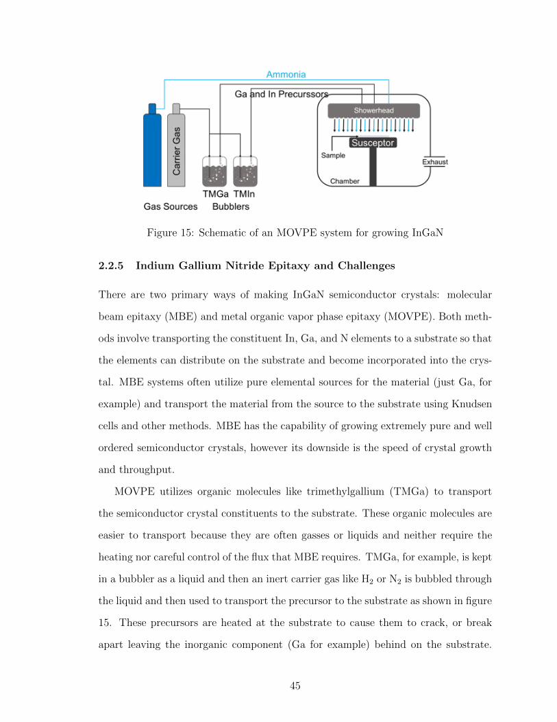
Figure 15: Schematic of an MOVPE system for growing InGaN
2.2.5 Indium Gallium Nitride Epitaxy and Challenges
There are two primary ways of making InGaN semiconductor crystals: molecular
beam epitaxy (MBE) and metal organic vapor phase epitaxy (MOVPE). Both meth-
ods involve transporting the constituent In, Ga, and N elements to a substrate so that
the elements can distribute on the substrate and become incorporated into the crys-
tal. MBE systems often utilize pure elemental sources for the material (just Ga, for
example) and transport the material from the source to the substrate using Knudsen
cells and other methods. MBE has the capability of growing extremely pure and well
ordered semiconductor crystals, however its downside is the speed of crystal growth
and throughput.
MOVPE utilizes organic molecules like trimethylgallium (TMGa) to transport
the semiconductor crystal constituents to the substrate. These organic molecules are
easier to transport because they are often gasses or liquids and neither require the
heating nor careful control of the flux that MBE requires. TMGa, for example, is kept
in a bubbler as a liquid and then an inert carrier gas like H2
or N2
is bubbled through
the liquid and then used to transport the precursor to the substrate as shown in figure
15. These precursors are heated at the substrate to cause them to crack, or break
apart leaving the inorganic component (Ga for example) behind on the substrate.
45
The organic components of the precursors are volatile and can be exhausted from
the growth chamber. MOVPE films can be of very high crystalline quality and can
be nearly atomically abrupt like MBE films despite challenges of defects introduced
by the atmosphere and growth temperature [64]. Furthermore, MOVPE systems can
achieve much higher growth rates and higher throughput than MBE reactors. This
is due in large part because MBE reactors must operate under high vacuum, and so
the uniformity of the deposited crystal is related to the kinetics of the sources being
deposited on the substrate and redistribution of adsorbed adatoms on the substrate.
MOVPE methods can operate at atmospheric pressure and so the uniformity of the
deposition is controlled by gas flow in the reactor and substrate heating. As a result
the crystal can be deposited on a much larger area at one time using MOVPE making
it the industrially preferred method of growing crystals like InGaN. Furthermore, the
films grown for this work were all done using MOVPE and so this will be the method
detailed in this thesis.
2.2.5.1 Lack of Lattice Matched Substrates
There are several challenges associated with the growth of InGaN solar cells. The
first challenge that cannot be overlooked is the lack of a lattice-matched substrate.
Generally for epitaxy to occur one must start with a crystal of the same lattice and
then add the components of the crystal slowly so that they can use the existing crystal
as a template for growth. Crystalline Si, for example, uses the Czochralski growth
method where a seed crystal is lowered into a crucible full of molten Si and slowly
drawn from the melt cooling and solidifying the Si around the seed into a large single
crystal ingot. It is not practicle to grow GaN from a melt. So the majority of InGaN
epitaxy is done by MOVPE. While other material systems, like Si or GaAs, use the
crystal that they are trying to grow as the template, this is not practical for GaN. Most
GaN epitaxy occurs using a Sapphire template [65]. Sapphire does have a hexagonal
46
crystal, but there is a 14% di↵erence of lattice spacing between the sapphire lattice
and GaN lattice and 29% between sapphire and InN. The GaN or InGaN will adopt
the Sapphire lattice during growth leading to intrinsic internal stress. As the crystal
grows thicker the elastic energy it takes to keep the accommodate the di↵erent lattice
parameter increases until it is energetically favorable to relieve the stress through
a defect in the crystal lattice. The thickness at which this this favorable is called
the critical thickness [66]. For sapphire this thickness is very small and so GaN on
sapphire often su↵ers from high concentrations of defects, typically on the order of
1⇥108 cm�3. To alleviate this problem other substrates have been considered for
GaN growth including SiC, ZnO, and Si (1 1 1). In spite of favorable lattice mismatch
and/or elastic properties of these substrates none have been shown to improve upon
the dislocation density of GaN on sapphire. The primary improvement over sapphire
has been in introduction of bulk GaN substrates, typically grown by hydride vapour
phase epitaxy (HVPE)[67]. The large scale manufacturing and adoption of these
substrates is still in it’s infancy making them prohibitively costly.
2.2.5.2 InGaN Phase Separation
Further complicating the growth of InGaN is the problem of phase separation. This
is the issue of InxGa1�xN alloys tending to separate into regions of higher and lower
In concentration, even for small In concentrations. This thermodynamics problem
caused by di↵erences in the chemical a�nity between GaN and InN resulting in solid
phase immiscibility. This miscibility gap can be expressed using a model of regular
solutions. Thus the change in Gibbs free energy, �G, of an InxGa1�xN alloy can be
expressed as:
�G = �Hm + RT (x ln(x) + (1 � x) ln(1 � x)) (37)
�Hm = ⌦ x (1 � x) (38)
47
The second term in the equation for the change in Gibbs free energy, RT (x ln(x) +
(1�x) ln(1�x)), is �T times the entropy of mixing. �Hm is the enthalpy of mixing
and is related to the heat released when the two end point binaries (GaN and InN in
this case) are mixed, and must be parameterized by ⌦, the regular solution interaction
parameter. This parameter can be calculated using a variety of models including a
semi-emperical delta-lattice-parameter model or a valence-force-field model[68]. This
model uses the energy to stretch or bend interatomic bonds to calculate the micro-
scopic strain energy in a regular solution. The enthalpy of mixing is the found by
summing over the di↵erent strain energies[69, 68]. Ho and Stringfellow found values
of ⌦ to be between 5.63 and 6.32 kcal/mole depending on whether the mixture was
Ga or In rich respectively[68].
This leads to a phase diagram that exhibits spinodal decomposition for InxGa1�xN
for compositions with x > 0.06 for InGaN grown at 800� C[68]. That means that
compositions greater than this are thermodynamically unstable. When the InGaN
mixtures decompose there will be regions that are In rich have a lower band gap
energy than the regions that are Ga rich and have a diode characteristic with a much
lower threshold voltage than the rest of the cell. This lower Voc will significantly
contribute to a degradation of solar cell e�ciency. This problem can be mitigated to
a certain extent by incorporating the e↵ect of elastic strain.
Growing pseudomorphically strained InGaN on GaN [70, 2], however it is not
practical to grow thick layers of strained InGaN due to the thin critical thickness.
Other methods for avoiding spinodal decomposition involve the insertion of thin layers
of GaN into the thicker InGaN which serve relieve the compressive strain and absorb
the excess In [71]. Also nano-selective area growth methods seem to be an attractive
alternative to bulk methods for some applications which require high In incorporation
[72].
Including strain into the model of a normal solution can be done my adding
48
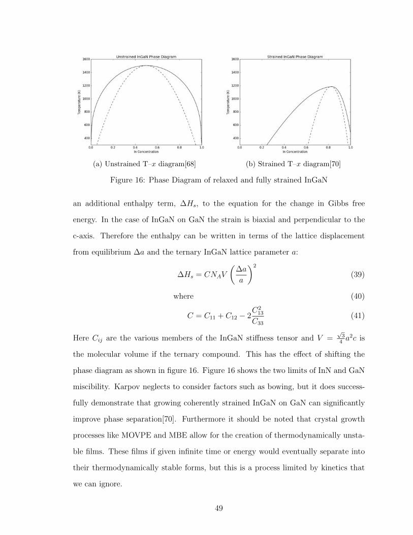
(a) Unstrained T–x diagram[68] (b) Strained T–x diagram[70]
Figure 16: Phase Diagram of relaxed and fully strained InGaN
an additional enthalpy term, �Hs, to the equation for the change in Gibbs free
energy. In the case of InGaN on GaN the strain is biaxial and perpendicular to the
c-axis. Therefore the enthalpy can be written in terms of the lattice displacement
from equilibrium �a and the ternary InGaN lattice parameter a:
�Hs = CNAV
✓�a
a
◆2
(39)
where (40)
C = C11
+ C12
� 2C2
13
C33
(41)
Here Cij are the various members of the InGaN sti↵ness tensor and V =p
3
4
a2c is
the molecular volume if the ternary compound. This has the e↵ect of shifting the
phase diagram as shown in figure 16. Figure 16 shows the two limits of InN and GaN
miscibility. Karpov neglects to consider factors such as bowing, but it does success-
fully demonstrate that growing coherently strained InGaN on GaN can significantly
improve phase separation[70]. Furthermore it should be noted that crystal growth
processes like MOVPE and MBE allow for the creation of thermodynamically unsta-
ble films. These films if given infinite time or energy would eventually separate into
their thermodynamically stable forms, but this is a process limited by kinetics that
we can ignore.
49
2.2.5.3 Di�culty of p-doping GaN
P-type doping of GaN was one of the early challenges facing researchers. The chal-
lenges were that undoped GaN is n-type as a result of native defects in in the crystal
and that GaN is a wide band gap material and so there were not many candidates
for dopants. The search for an e↵ective dopant remained elusive until 1989 when
Akasaki demonstrated p-type conduction in Mg compensated films activated by elec-
tron irradiation[73, 74]. Shortly there after Nakamura was able to demonstrate Mg
doping via a two step process in which the film is grown with Mg (usually from
a bis(cyclopentadienyl)magnesium or Cp2
Mg precursor) and then annealed at high
temperature under nitrogen[75]. This is the process that is used to this day for doping
GaN.
There are, however, some tradeo↵s to consider to Mg doping of GaN. Firstly
the activation energy of Mg is 160 meV, which is comparatively high for dopants.
Consider B doping in Si, for example, where the activation energy is 45 meV. This
results in only 1–2% of the Mg dopants contributing to the p-type conduction. Thus
to compensate for the intrinsic n-type quality of the film and for the low acceptor
rate of Mg high concentrations (1E20 cm�2) are required in order to for the GaN film
to display p-type conduction. This has detrimental e↵ects to the GaN film quality.
Furthermore, interstitial hydrogen has been shown to form a complex with Mg in
the crystal which deactivates the dopant. This is why the annealing occurs in a
nitrogen free atmosphere. This causes an additional problem as without a nitrogen
precursor like ammonia (NH3
) under high temperature the III-N bond can be broken
and nitrogen can desorb from the crystal further reducing crystalline quality.
The high temperature growth and annealing of p-type GaN introduces another
practical issue for the growth of InGaN/GaN solar cells. P-type GaN is preferred for
making the PN junction above the InGaN absorber layers to p-type InGaN because
Mg doping in InGaN can contribute to phase separation [2]. The In-N bond strength
50
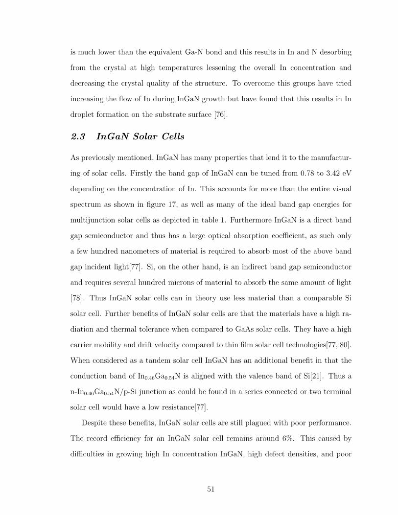
is much lower than the equivalent Ga-N bond and this results in In and N desorbing
from the crystal at high temperatures lessening the overall In concentration and
decreasing the crystal quality of the structure. To overcome this groups have tried
increasing the flow of In during InGaN growth but have found that this results in In
droplet formation on the substrate surface [76].
2.3 InGaN Solar Cells
As previously mentioned, InGaN has many properties that lend it to the manufactur-
ing of solar cells. Firstly the band gap of InGaN can be tuned from 0.78 to 3.42 eV
depending on the concentration of In. This accounts for more than the entire visual
spectrum as shown in figure 17, as well as many of the ideal band gap energies for
multijunction solar cells as depicted in table 1. Furthermore InGaN is a direct band
gap semiconductor and thus has a large optical absorption coe�cient, as such only
a few hundred nanometers of material is required to absorb most of the above band
gap incident light[77]. Si, on the other hand, is an indirect band gap semiconductor
and requires several hundred microns of material to absorb the same amount of light
[78]. Thus InGaN solar cells can in theory use less material than a comparable Si
solar cell. Further benefits of InGaN solar cells are that the materials have a high ra-
diation and thermal tolerance when compared to GaAs solar cells. They have a high
carrier mobility and drift velocity compared to thin film solar cell technologies[77, 80].
When considered as a tandem solar cell InGaN has an additional benefit in that the
conduction band of In0.46
Ga0.54
N is aligned with the valence band of Si[21]. Thus a
n-In0.46
Ga0.54
N/p-Si junction as could be found in a series connected or two terminal
solar cell would have a low resistance[77].
Despite these benefits, InGaN solar cells are still plagued with poor performance.
The record e�ciency for an InGaN solar cell remains around 6%. This caused by
di�culties in growing high In concentration InGaN, high defect densities, and poor
51
(a) Band gap vs lattice parameter(b) Optical Absorption for 16% In and 3.1eV photons[79]
Figure 17: Band gap of InGaN compared to other solar cell materials and the opticalabsorption properties of InGaN compared to Si
metal contacts to the p-type GaN resulting in large series resistances.
The promise of III-nitrides as photovoltaics has been well documented and at-
tracted the attention of many researchers[80]. One can characterize the solar cells
into a variety of categories: bulk vs quantum-structured cells and heterojunction vs
homojunction cells. The bulk cells consist of a single material absorber of GaN or In-
GaN, where the quantum-structured cells utilize compositional variations within the
absorber layer to create quantum wells, superlattices, or other quantum structures.
The quantum structure has the benefit of utilizing high In content layers pseudo-
morphically strained to the GaN template, thus maintaining the crystal quality and
having strong light absorption within the quantum wells [81]. However the over-
all thickness of the InGaN quantum structures is limited, and thus much of the light
passes through the InGaN layers unabsorbed. The homojunction photovoltaic devices
are made using combinations of p-type, intrinsic, and n-type InGaN. Heterojunction
devices are made by combining an InGaN absorber with n-GaN and/or p-GaN. The
heterojunction devices typically have a structure of p-GaN/nid-InGaN/n-GaN. The
homojunction devices usually display lower collection e�ciencies and thus degraded
short circuit currents compared to heterojunction devices [82]. This translates to
52
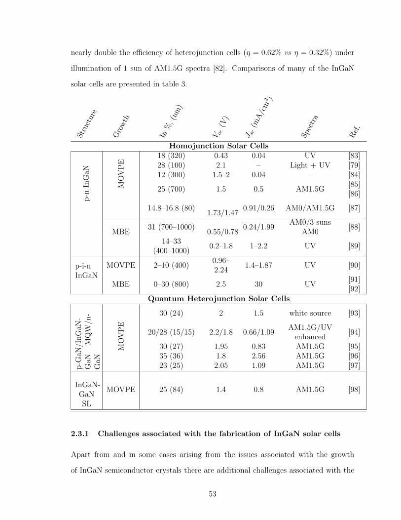
nearly double the e�ciency of heterojunction cells (⌘ = 0.62% vs ⌘ = 0.32%) under
illumination of 1 sun of AM1.5G spectra [82]. Comparisons of many of the InGaN
solar cells are presented in table 3.St
ruct
ure
Gro
wth
In%
, (nm
)
V oc
(V)
J sc
(mA/c
m2
)
Spec
tra
Ref.
Homojunction Solar Cells
p-n
InG
aN
MO
VP
E
18 (320) 0.43 0.04 UV [83]28 (100) 2.1 – Light + UV [79]12 (300) 1.5–2 0.04 – [84]
25 (700) 1.5 0.5 AM1.5G[85][86]
14.8–16.8 (80)1.73/1.47
0.91/0.26 AM0/AM1.5G [87]
MBE31 (700–1000)
0.55/0.780.24/1.99
AM0/3 sunsAM0
[88]
14–33(400–1000)
0.2–1.8 1–2.2 UV [89]
p-i-nInGaN
MOVPE 2–10 (400)0.96–2.24
1.4–1.87 UV [90]
MBE 0–30 (800) 2.5 30 UV[91][92]
Quantum Heterojunction Solar Cells
p-G
aN/I
nG
aN-
GaN
MQ
W/n
-G
aN
30 (24) 2 1.5 white source [93]
20/28 (15/15) 2.2/1.8 0.66/1.09AM1.5G/UV
enhanced[94]
30 (27) 1.95 0.83 AM1.5G [95]35 (36) 1.8 2.56 AM1.5G [96]
MO
VP
E
23 (25) 2.05 1.09 AM1.5G [97]
InGaN-GaNSL
MOVPE 25 (84) 1.4 0.8 AM1.5G [98]
2.3.1 Challenges associated with the fabrication of InGaN solar cells
Apart from and in some cases arising from the issues associated with the growth
of InGaN semiconductor crystals there are additional challenges associated with the
53
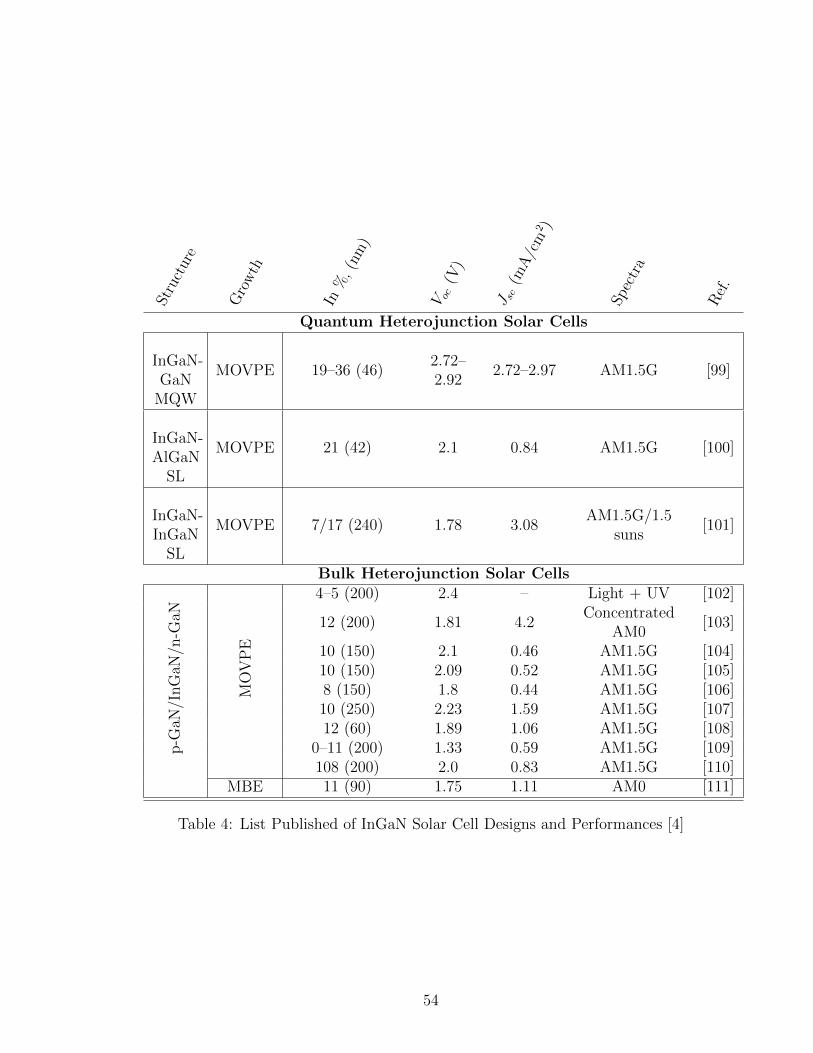
Stru
ctur
e
Gro
wth
In%
, (nm
)
V oc
(V)
J sc
(mA/c
m2
)
Spec
tra
Ref.
Quantum Heterojunction Solar Cells
InGaN-GaN
MQW
MOVPE 19–36 (46)2.72–2.92
2.72–2.97 AM1.5G [99]
InGaN-AlGaN
SL
MOVPE 21 (42) 2.1 0.84 AM1.5G [100]
InGaN-InGaN
SL
MOVPE 7/17 (240) 1.78 3.08AM1.5G/1.5
suns[101]
Bulk Heterojunction Solar Cells
p-G
aN/I
nG
aN/n
-GaN
MO
VP
E
4–5 (200) 2.4 – Light + UV [102]
12 (200) 1.81 4.2Concentrated
AM0[103]
10 (150) 2.1 0.46 AM1.5G [104]10 (150) 2.09 0.52 AM1.5G [105]8 (150) 1.8 0.44 AM1.5G [106]10 (250) 2.23 1.59 AM1.5G [107]12 (60) 1.89 1.06 AM1.5G [108]
0–11 (200) 1.33 0.59 AM1.5G [109]108 (200) 2.0 0.83 AM1.5G [110]
MBE 11 (90) 1.75 1.11 AM0 [111]
Table 4: List Published of InGaN Solar Cell Designs and Performances [4]
54
fabrication of InGaN solar cells. Firstly, intrinsic GaN (often called non-intentionally
doped or nid-GaN) is a strong n-type semiconductor with a carrier concentration
ranging from 1E16 to 1E18 [112]. The background concentration can be compensated
for by the inclusion of Fe during nid-GaN growth [113, 114]. The high background
would not be an insurmountable problem, except that it is quite di�cult to dope
GaN p-type [2]. Mg is the most common p-type dopant for GaN, but of the acceptors
used it also has the largest activation energy [2]. This results in only between 1% and
3% of the Mg acceptors in the crystal actively contributing to p-type conductivity at
room temperature. Furthermore, there is the risk of forming hydrogen complexes with
native defects in GaN like nitrogen vacancies, VN -H, or with the Mg dopants Mg-H
complexes which can deactivate the Mg dopants and compensate for p-doping [115,
116]. As there is hydrogen present during the epitaxial growth process a prolonged
annealing step in a hydrogen-free ambient is required. This in turn, may lead to a
desorption of nitrogen introducing defects into the crystal. p-GaN’s sensitivity to
hydrogen also has ramifications to processes further down the line as well as it is
common to use SiO2
as a dielectric but many recipes for depositing and etching SiO2
also include hydrogen. Thus if used, the material must be annealed to reactivate the
Mg dopants.
A further challenge involves v-defects. These are defects that originate at thread-
ing or screw dislocations within the crystal. Growth at the site of the defect occurs
slower than in the bulk resulting in a V-shaped hexagonal pit on the surface. When
contacting the top surface of the structure metal can seep into the pit and create a
short-circuit path to the bottom layers. The best alternative to this is to improve the
film quality to avoid v-defects. However as solar cell devices are quite large compared
to LEDs (1 cm2 vs 15 mm2) or other devices made with GaN materials the elimina-
tion of v-defects may be an unobtainable goal. Further methods of compensating for
the v-defects include filling the defects with a spin-on hydrogen silsesquioxane (HSQ)
55
resin [2].
The metallization of n-type and p-type GaN also presents challenges to solar cell
fabrication. Specifically, there is a di�culty obtaining ohmic contacts with n and
p-type GaN. Ohmic contacts are preferred for solar cells because the alternative,
Schottky contacts result in a barrier to collecting the charge carriers which reduces
the solar cell e�ciency. The metals used to make ohmic contact to need to have
the proper work function. On n-type GaN ohmic contact is typically achieved with
low work function metals like Ti or Al [117, 118, 119]. Further improvements on
n-type GaN can be made by depositing an alloy of Ti and Al as well as by annealing
[120]. Formation of an ohmic contact in p-type GaN, however, is extremely di�culty.
There are not many metals with the appropriate work function to form an ohmic
contact on p-type GaN. This problem is exacerbated by low p-type activated dopant
concentrations. Thus if a Schottky contact is formed the barrier to carriers is wide and
the tunneling e�ciency is low. Ohmic contact formation on p-type GaN is extensively
studied however [121]. Typically thin layers of Ni and Au are used to make the
contacts [122, 123]. These contacts are then annealed to improve their resistivity.
Finally, there are challenges that arise from the use of dry etching in the processing
of the solar cells. Dry etching introduces damage to the surface of the semiconductor
[124]. This damage is responsible for degrading solar cell performance by introducing
donor like traps near the surface, further degrading the p-type GaN carrier concen-
tration [124]. However, the e↵ect of the etch damage can be lessened by chemical or
annealing treatments [124].
2.3.2 Semibulk InGaN for Photovoltaics
One of the primary blocking points of high e�ciency InGaN solar cells is the challenge
of growing thick, high In content InGaN[4]. The lack of high In content results in the
material being transparent to most of the solar spectrum and as a result InGaN solar
56
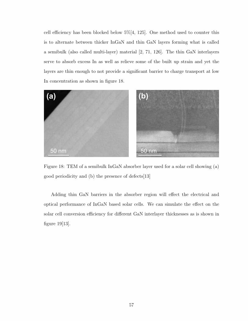
cell e�ciency has been blocked below 5%[4, 125]. One method used to counter this
is to alternate between thicker InGaN and thin GaN layers forming what is called
a semibulk (also called multi-layer) material [2, 71, 126]. The thin GaN interlayers
serve to absorb excess In as well as relieve some of the built up strain and yet the
layers are thin enough to not provide a significant barrier to charge transport at low
In concentration as shown in figure 18.
(b)
50 nm 50 nm
(a)
Figure 18: TEM of a semibulk InGaN absorber layer used for a solar cell showing (a)
good periodicity and (b) the presence of defects[13]
Adding thin GaN barriers in the absorber region will e↵ect the electrical and
optical performance of InGaN based solar cells. We can simulate the e↵ect on the
solar cell conversion e�ciency for di↵erent GaN interlayer thicknesses as is shown in
figure 19[13].
57
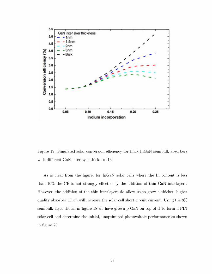
Figure 19: Simulated solar conversion e�ciency for thick InGaN semibulk absorbers
with di↵erent GaN interlayer thickness[13]
As is clear from the figure, for InGaN solar cells where the In content is less
than 10% the CE is not strongly e↵ected by the addition of thin GaN interlayers.
However, the addition of the thin interlayers do allow us to grow a thicker, higher
quality absorber which will increase the solar cell short circuit current. Using the 8%
semibulk layer shown in figure 18 we have grown p-GaN on top of it to form a PIN
solar cell and determine the initial, unoptimized photovoltaic performance as shown
in figure 20.
58
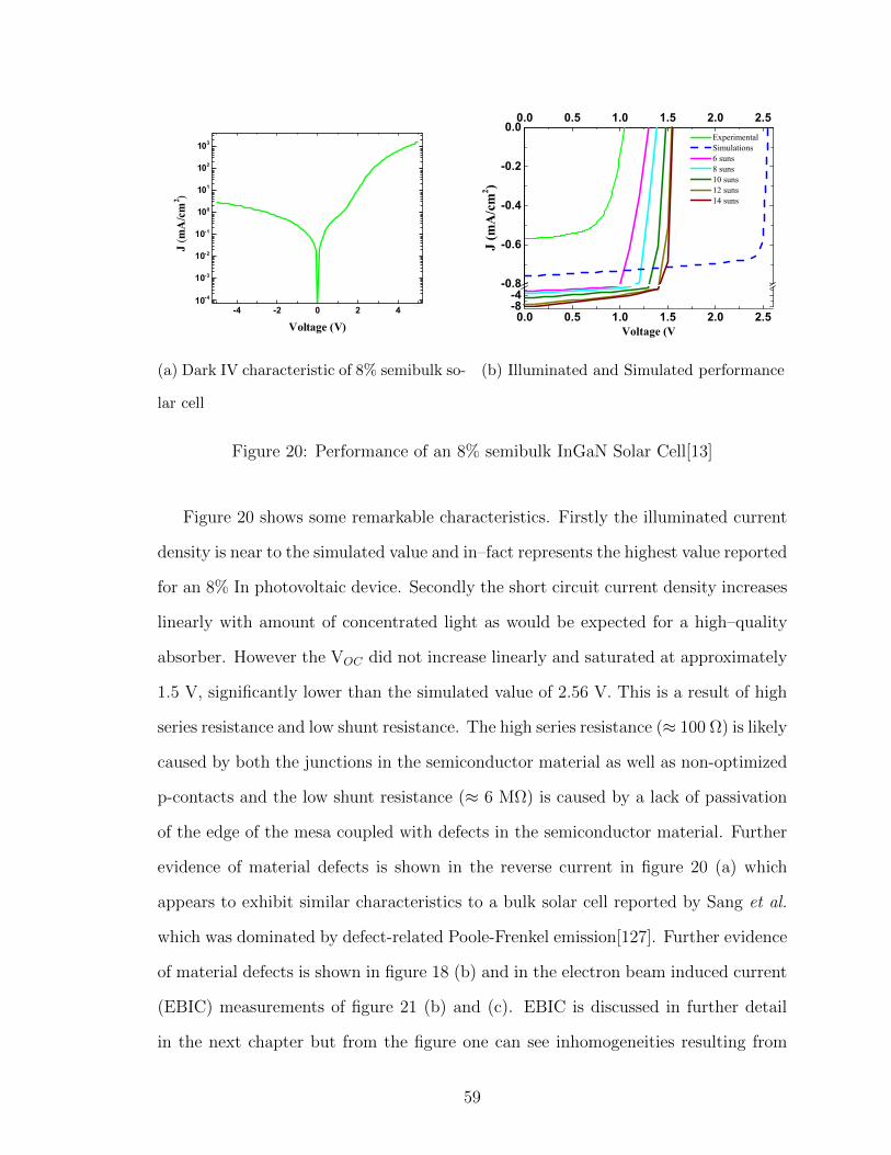
-4 -2 0 2 410-4
10-3
10-2
10-1
100
101
102
103
J (m
A/c
m2 )
Voltage (V)
(a) Dark IV characteristic of 8% semibulk so-
lar cell
0.0 0.5 1.0 1.5 2.0 2.5-8-4
-0.8
-0.6
-0.4
-0.2
0.00.0 0.5 1.0 1.5 2.0 2.5
Experimental Simulations 6 suns 8 suns 10 suns 12 suns 14 suns
J (m
A/c
m2 )
Voltage (V
(b) Illuminated and Simulated performance
Figure 20: Performance of an 8% semibulk InGaN Solar Cell[13]
Figure 20 shows some remarkable characteristics. Firstly the illuminated current
density is near to the simulated value and in–fact represents the highest value reported
for an 8% In photovoltaic device. Secondly the short circuit current density increases
linearly with amount of concentrated light as would be expected for a high–quality
absorber. However the VOC did not increase linearly and saturated at approximately
1.5 V, significantly lower than the simulated value of 2.56 V. This is a result of high
series resistance and low shunt resistance. The high series resistance (⇡ 100 ⌦) is likely
caused by both the junctions in the semiconductor material as well as non-optimized
p-contacts and the low shunt resistance (⇡ 6 M⌦) is caused by a lack of passivation
of the edge of the mesa coupled with defects in the semiconductor material. Further
evidence of material defects is shown in the reverse current in figure 20 (a) which
appears to exhibit similar characteristics to a bulk solar cell reported by Sang et al.
which was dominated by defect-related Poole-Frenkel emission[127]. Further evidence
of material defects is shown in figure 18 (b) and in the electron beam induced current
(EBIC) measurements of figure 21 (b) and (c). EBIC is discussed in further detail
in the next chapter but from the figure one can see inhomogeneities resulting from
59
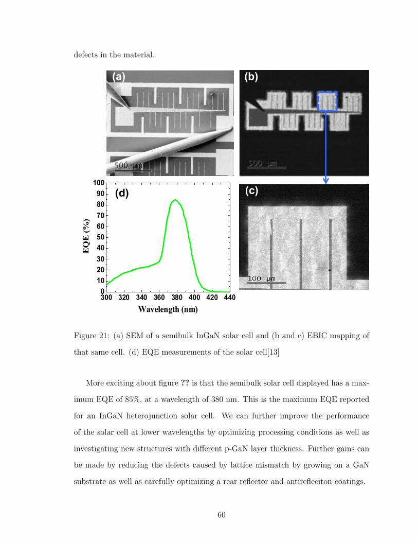
defects in the material.
(a) (b)
(c)
300 320 340 360 380 400 420 4400102030405060708090100
EQ
E (%
)
Wavelength (nm)
(d)
Figure 21: (a) SEM of a semibulk InGaN solar cell and (b and c) EBIC mapping of
that same cell. (d) EQE measurements of the solar cell[13]
More exciting about figure ?? is that the semibulk solar cell displayed has a max-
imum EQE of 85%, at a wavelength of 380 nm. This is the maximum EQE reported
for an InGaN heterojunction solar cell. We can further improve the performance
of the solar cell at lower wavelengths by optimizing processing conditions as well as
investigating new structures with di↵erent p-GaN layer thickness. Further gains can
be made by reducing the defects caused by lattice mismatch by growing on a GaN
substrate as well as carefully optimizing a rear reflector and antirefleciton coatings.
60

2.3.3 InGaN Tandem solar cells
InGaN/Si tandem solar cells have the possibility to combine the benefits of both ma-
terials. Simulations suggest that e�ciencies of a InGaN/Si solar cell could be as high
as 31%[21]. Furthermore the calculated band alignments of In0.45
Ga0.55
N/p-Si could
result in a two–terminal device without the need for a tunnel junction which would
reduce the series resistance of the device and further boost collection e�ciency[128].
Growing directly on Si is a problem for InGaN materials as there is a large lattice
mismatch between Si (111) and InGaN structures. Furthermore is is extremely di�-
cult to grow well crystallized InGaN on Si because Si has a cubic lattice and InGaN
is typically grown in the hexagonal lattice configuration. El-Huni et al. suggest grow-
ing InGaN on a ZnO bu↵er as this has shown to reduce defect propagation into the
nitride material [14, 129]. In order to achieve current matching and implement a high
e�ciency InGaN Si tandem the In content needs to be around 50%. Furthermore a
tunnel junction must be realized in Si. The resulting simulated energy band diagram
and solar cell characteristic is shown in figure 22.
(a) Simulated energy band diagram (b) Simulated solar cell performance
Figure 22: Realistic simulated In0.5Ga
0.5N/Si monolithic tandem solar cell[14]
The performance of such a solar cell is simulated to be over 30%. However in
reality there are many technical challenges associated with realizing such a structure.
61
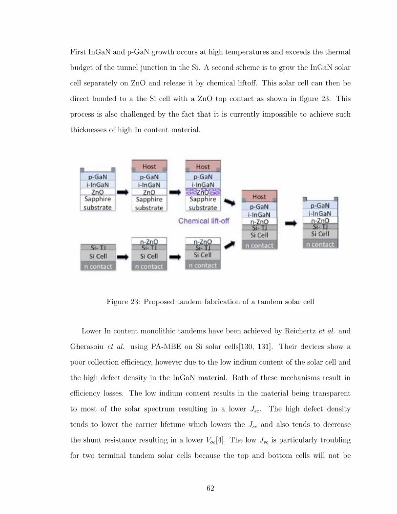
First InGaN and p-GaN growth occurs at high temperatures and exceeds the thermal
budget of the tunnel junction in the Si. A second scheme is to grow the InGaN solar
cell separately on ZnO and release it by chemical lifto↵. This solar cell can then be
direct bonded to a the Si cell with a ZnO top contact as shown in figure 23. This
process is also challenged by the fact that it is currently impossible to achieve such
thicknesses of high In content material.
Figure 23: Proposed tandem fabrication of a tandem solar cell
Lower In content monolithic tandems have been achieved by Reichertz et al. and
Gherasoiu et al. using PA-MBE on Si solar cells[130, 131]. Their devices show a
poor collection e�ciency, however due to the low indium content of the solar cell and
the high defect density in the InGaN material. Both of these mechanisms result in
e�ciency losses. The low indium content results in the material being transparent
to most of the solar spectrum resulting in a lower Jsc. The high defect density
tends to lower the carrier lifetime which lowers the Jsc and also tends to decrease
the shunt resistance resulting in a lower Voc[4]. The low Jsc is particularly troubling
for two terminal tandem solar cells because the top and bottom cells will not be
62
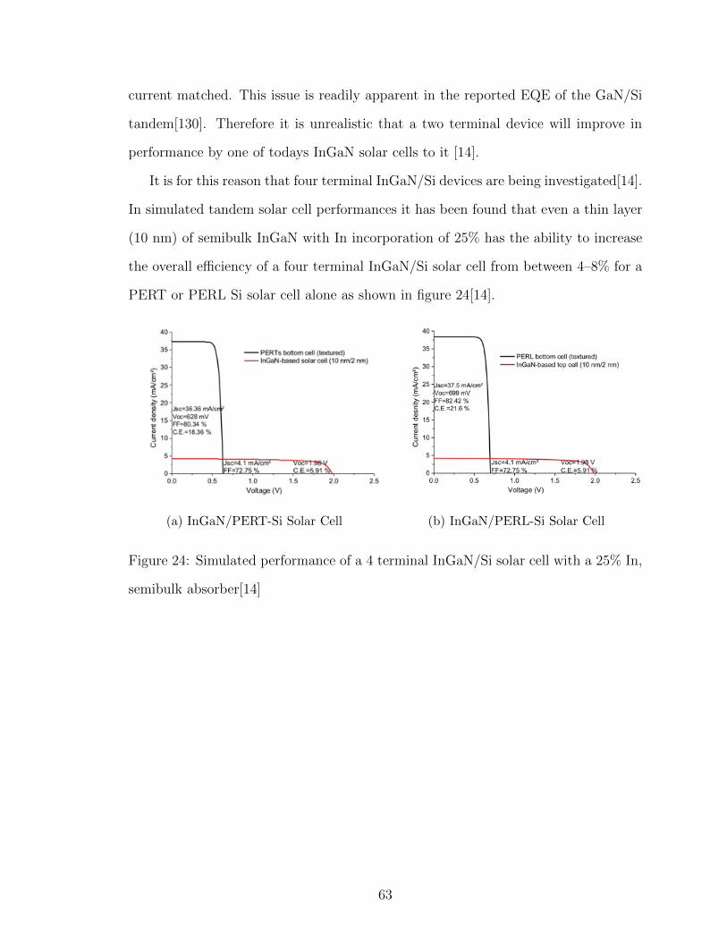
current matched. This issue is readily apparent in the reported EQE of the GaN/Si
tandem[130]. Therefore it is unrealistic that a two terminal device will improve in
performance by one of todays InGaN solar cells to it [14].
It is for this reason that four terminal InGaN/Si devices are being investigated[14].
In simulated tandem solar cell performances it has been found that even a thin layer
(10 nm) of semibulk InGaN with In incorporation of 25% has the ability to increase
the overall e�ciency of a four terminal InGaN/Si solar cell from between 4–8% for a
PERT or PERL Si solar cell alone as shown in figure 24[14].
(a) InGaN/PERT-Si Solar Cell (b) InGaN/PERL-Si Solar Cell
Figure 24: Simulated performance of a 4 terminal InGaN/Si solar cell with a 25% In,
semibulk absorber[14]
63
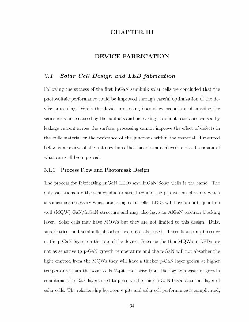
CHAPTER III
DEVICE FABRICATION
3.1 Solar Cell Design and LED fabrication
Following the success of the first InGaN semibulk solar cells we concluded that the
photovoltaic performance could be improved through careful optimization of the de-
vice processing. While the device processing does show promise in decreasing the
series resistance caused by the contacts and increasing the shunt resistance caused by
leakage current across the surface, processing cannot improve the e↵ect of defects in
the bulk material or the resistance of the junctions within the material. Presented
below is a review of the optimizations that have been achieved and a discussion of
what can still be improved.
3.1.1 Process Flow and Photomask Design
The process for fabricating InGaN LEDs and InGaN Solar Cells is the same. The
only variations are the semiconductor structure and the passivation of v-pits which
is sometimes necessary when processing solar cells. LEDs will have a multi-quantum
well (MQW) GaN/InGaN structure and may also have an AlGaN electron blocking
layer. Solar cells may have MQWs but they are not limited to this design. Bulk,
superlattice, and semibulk absorber layers are also used. There is also a di↵erence
in the p-GaN layers on the top of the device. Because the thin MQWs in LEDs are
not as sensitive to p-GaN growth temperature and the p-GaN will not absorber the
light emitted from the MQWs they will have a thicker p-GaN layer grown at higher
temperature than the solar cells V-pits can arise from the low temperature growth
conditions of p-GaN layers used to preserve the thick InGaN based absorber layer of
solar cells. The relationship between v-pits and solar cell performance is complicated,
64
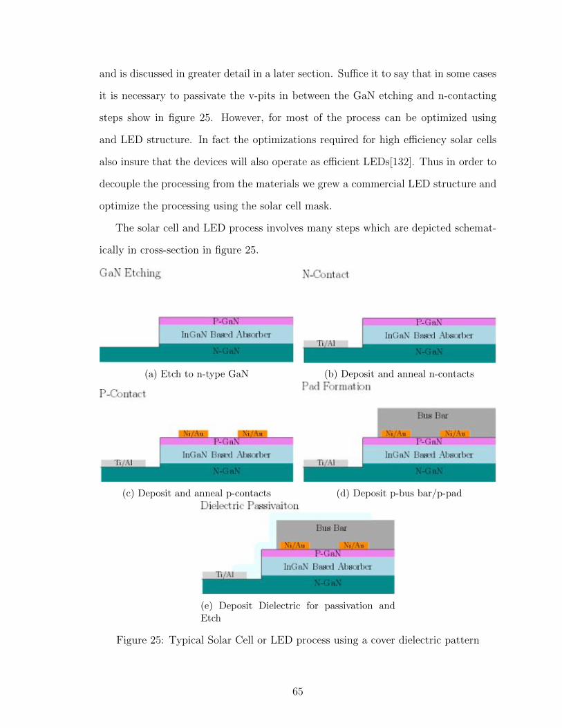
and is discussed in greater detail in a later section. Su�ce it to say that in some cases
it is necessary to passivate the v-pits in between the GaN etching and n-contacting
steps show in figure 25. However, for most of the process can be optimized using
and LED structure. In fact the optimizations required for high e�ciency solar cells
also insure that the devices will also operate as e�cient LEDs[132]. Thus in order to
decouple the processing from the materials we grew a commercial LED structure and
optimize the processing using the solar cell mask.
The solar cell and LED process involves many steps which are depicted schemat-
ically in cross-section in figure 25.
(a) Etch to n-type GaN (b) Deposit and anneal n-contacts
(c) Deposit and anneal p-contacts (d) Deposit p-bus bar/p-pad
(e) Deposit Dielectric for passivation andEtch
Figure 25: Typical Solar Cell or LED process using a cover dielectric pattern
65
In this chapter we deconstruct each processing step and discuss optimizations that
we have performed. It is impractical to investigate every parameter and impossible
to follow every pathway when optimizing the processing. This is why a through
literature review has been included in the discussion of each process step. In this
way context into the key parameters and figures of merit can be introduced for each
processing step. It is also meant to allow the discussion of each step to stand alone
as reference and a starting point that can be built upon by later PhD students.
The presented process flow is just one of many possible routes that may be taken
to achieve similar results. For example the presented process flow includes a dielectric
layer encapsulating the entire diode at the end of the process. Mesa passivation does
not have to occur at the end and often passivation is achieved immediately after
etching. This is why we provided for the possibility to try three di↵erent passivation
schemes. We label these three schemes: cover, edge, and surface passivation and they
are depicted schematically in figure 26.
(a) Edge Passivation 3D (b) Surface Passivation 3D (c) Cover Passivation 3D
P
IN
Semiconductor
Bus Bar
Bus Bar Ni/Au Ni/Au
Ti/Al
Edge Passivationw
(d) Edge Passivation
P
IN
Semiconductor
Bus Bar
Bus Bar Ni/Au Ni/Au
Ti/Al
Surface Passivation
w
(e) Surface Passivation
P
IN
Semiconductor
Bus Bar
Bus Bar Ni/Au Ni/Au
Ti/Al
Cover Passivation d
(f) Cover Passivation
Figure 26: Cover, Surface, and Edge Passivation designs
The edge passivation scheme passivates only the edge of the mesa. This prevents
66
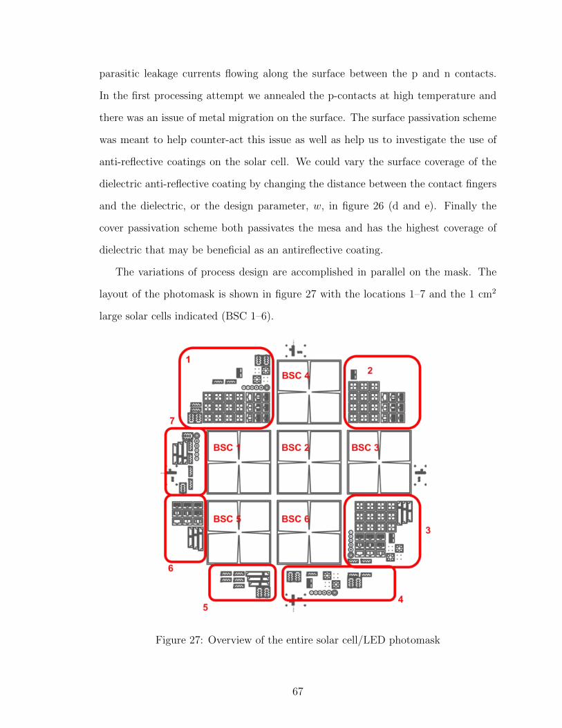
parasitic leakage currents flowing along the surface between the p and n contacts.
In the first processing attempt we annealed the p-contacts at high temperature and
there was an issue of metal migration on the surface. The surface passivation scheme
was meant to help counter-act this issue as well as help us to investigate the use of
anti-reflective coatings on the solar cell. We could vary the surface coverage of the
dielectric anti-reflective coating by changing the distance between the contact fingers
and the dielectric, or the design parameter, w, in figure 26 (d and e). Finally the
cover passivation scheme both passivates the mesa and has the highest coverage of
dielectric that may be beneficial as an antireflective coating.
The variations of process design are accomplished in parallel on the mask. The
layout of the photomask is shown in figure 27 with the locations 1–7 and the 1 cm2
large solar cells indicated (BSC 1–6).
Figure 27: Overview of the entire solar cell/LED photomask
67
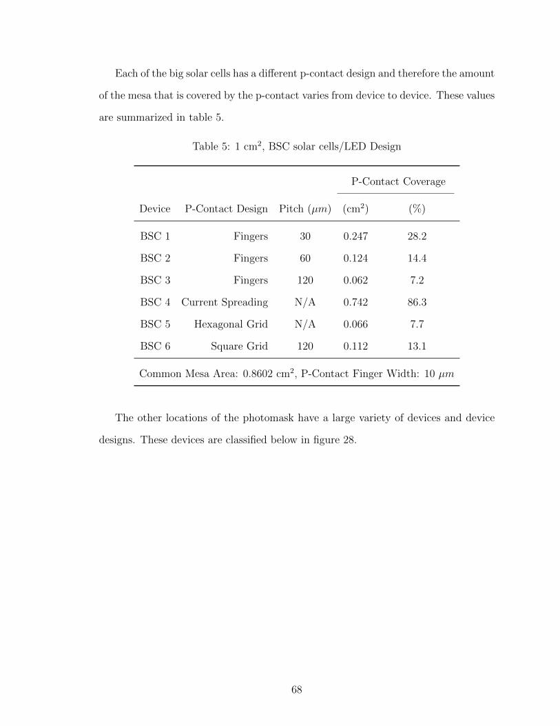
Each of the big solar cells has a di↵erent p-contact design and therefore the amount
of the mesa that is covered by the p-contact varies from device to device. These values
are summarized in table 5.
Table 5: 1 cm2, BSC solar cells/LED Design
P-Contact Coverage
Device P-Contact Design Pitch (µm) (cm2) (%)
BSC 1 Fingers 30 0.247 28.2
BSC 2 Fingers 60 0.124 14.4
BSC 3 Fingers 120 0.062 7.2
BSC 4 Current Spreading N/A 0.742 86.3
BSC 5 Hexagonal Grid N/A 0.066 7.7
BSC 6 Square Grid 120 0.112 13.1
Common Mesa Area: 0.8602 cm2, P-Contact Finger Width: 10 µm
The other locations of the photomask have a large variety of devices and device
designs. These devices are classified below in figure 28.
68
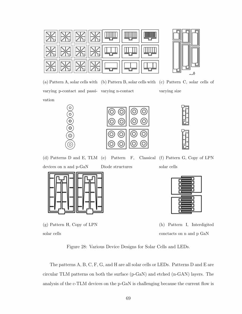
(a) Pattern A, solar cells with
varying p-contact and passi-
vation
(b) Pattern B, solar cells with
varying n-contact
(c) Pattern C, solar cells of
varying size
(d) Patterns D and E, TLM
devices on n and p-GaN
(e) Pattern F, Classical
Diode structures
(f) Pattern G, Copy of LPN
solar cells
(g) Pattern H, Copy of LPN
solar cells
(h) Pattern I, Interdigited
conctacts on n and p GaN
Figure 28: Various Device Designs for Solar Cells and LEDs.
The patterns A, B, C, F, G, and H are all solar cells or LEDs. Patterns D and E are
circular TLM patterns on both the surface (p-GaN) and etched (n-GAN) layers. The
analysis of the c-TLM devices on the p-GaN is challenging because the current flow is
69
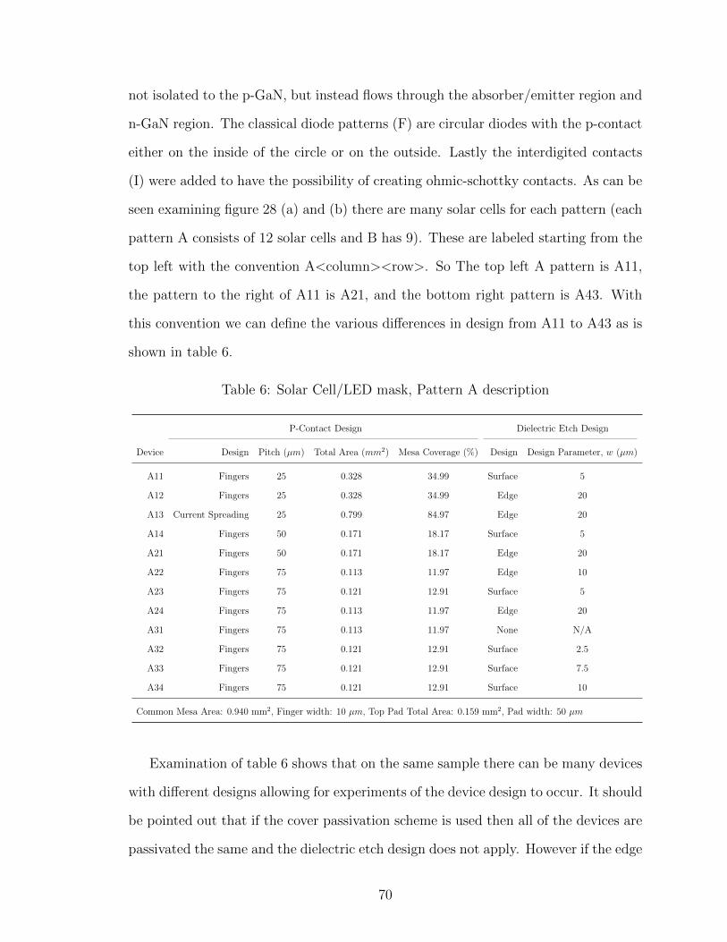
not isolated to the p-GaN, but instead flows through the absorber/emitter region and
n-GaN region. The classical diode patterns (F) are circular diodes with the p-contact
either on the inside of the circle or on the outside. Lastly the interdigited contacts
(I) were added to have the possibility of creating ohmic-schottky contacts. As can be
seen examining figure 28 (a) and (b) there are many solar cells for each pattern (each
pattern A consists of 12 solar cells and B has 9). These are labeled starting from the
top left with the convention A<column><row>. So The top left A pattern is A11,
the pattern to the right of A11 is A21, and the bottom right pattern is A43. With
this convention we can define the various di↵erences in design from A11 to A43 as is
shown in table 6.
Table 6: Solar Cell/LED mask, Pattern A description
P-Contact Design Dielectric Etch Design
Device Design Pitch (µm) Total Area (mm2) Mesa Coverage (%) Design Design Parameter, w (µm)
A11 Fingers 25 0.328 34.99 Surface 5
A12 Fingers 25 0.328 34.99 Edge 20
A13 Current Spreading 25 0.799 84.97 Edge 20
A14 Fingers 50 0.171 18.17 Surface 5
A21 Fingers 50 0.171 18.17 Edge 20
A22 Fingers 75 0.113 11.97 Edge 10
A23 Fingers 75 0.121 12.91 Surface 5
A24 Fingers 75 0.113 11.97 Edge 20
A31 Fingers 75 0.113 11.97 None N/A
A32 Fingers 75 0.121 12.91 Surface 2.5
A33 Fingers 75 0.121 12.91 Surface 7.5
A34 Fingers 75 0.121 12.91 Surface 10
Common Mesa Area: 0.940 mm2, Finger width: 10 µm, Top Pad Total Area: 0.159 mm2, Pad width: 50 µm
Examination of table 6 shows that on the same sample there can be many devices
with di↵erent designs allowing for experiments of the device design to occur. It should
be pointed out that if the cover passivation scheme is used then all of the devices are
passivated the same and the dielectric etch design does not apply. However if the edge
70
and surface passivation schemes used, then there is variation between two devices with
di↵erent design parameter, w, as described in figure 26 (d) and (e).
Pattern B has devices where the inclusion of the n-contact inside the mesa varies
from zero (n-contact just on the surrounding device) to fifteen but the p-contact
pitch and dielectric design remain constant. Pattern C has no n-contact inclusions,
no variation of p-contact or dielectric etching but instead the size of the mesa is varied
along with the bus bar. The thought being that if there are non-uniformities in the
growth of the solar cells or LEDs (like a low density of v-pits) that have roughly the
same density as the size of the devices, then by varying the device size we may, over
time, be able to determine the e↵ect of these non-uniformities.
3.2 GaN Etching
Etching of GaN is accomplished using a Cl–based plasma in a commercially available
inductively coupled plasma (ICP) etcher. Plasma etching, or dry etching, involves
the balancing of two mechanisms. First there is a physical etching process in which
the plasma is accelerated towards the substrate (III-Nitride materials in this case)
and they physical impingement of the ionized species with the substrate can etch
the material. This process is highly directional and only the exposed surface will
be etched physically. Secondly there is a chemical etching caused by molecules in
the plasma reacting with the substrate. The reaction products are volatile and can
be exhausted from the etching chamber. The chemical process is more isotropic
compared to physical etching, meaning that the reaction can occur laterally, tending
to widen etch trenches. The physical reaction doesn’t “care” whether the material is
nitride, oxide, metal, or photoresist and will remove all of them. Thus the physical
etching is not very selective. Furthermore reaction products sputtered from the mask
by physical etching may not be volatile and can land on the substrate where it will
slow etching progress in that area. This leads to a higher roughness on the etched
71
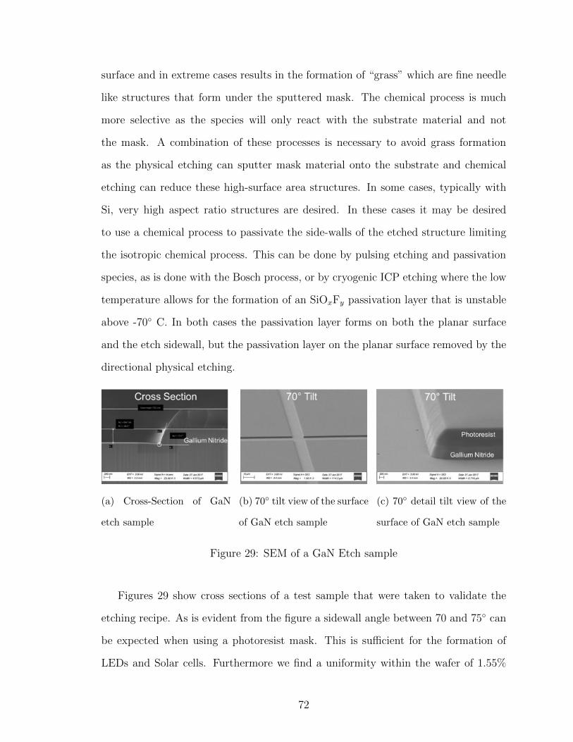
surface and in extreme cases results in the formation of “grass” which are fine needle
like structures that form under the sputtered mask. The chemical process is much
more selective as the species will only react with the substrate material and not
the mask. A combination of these processes is necessary to avoid grass formation
as the physical etching can sputter mask material onto the substrate and chemical
etching can reduce these high-surface area structures. In some cases, typically with
Si, very high aspect ratio structures are desired. In these cases it may be desired
to use a chemical process to passivate the side-walls of the etched structure limiting
the isotropic chemical process. This can be done by pulsing etching and passivation
species, as is done with the Bosch process, or by cryogenic ICP etching where the low
temperature allows for the formation of an SiOxFy passivation layer that is unstable
above -70� C. In both cases the passivation layer forms on both the planar surface
and the etch sidewall, but the passivation layer on the planar surface removed by the
directional physical etching.
(a) Cross-Section of GaN
etch sample
(b) 70� tilt view of the surface
of GaN etch sample
(c) 70� detail tilt view of the
surface of GaN etch sample
Figure 29: SEM of a GaN Etch sample
Figures 29 show cross sections of a test sample that were taken to validate the
etching recipe. As is evident from the figure a sidewall angle between 70 and 75� can
be expected when using a photoresist mask. This is su�cient for the formation of
LEDs and Solar cells. Furthermore we find a uniformity within the wafer of 1.55%
72
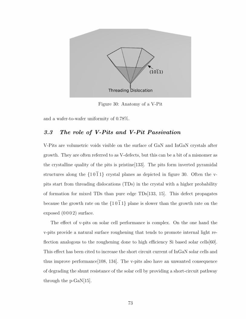
Figure 30: Anatomy of a V-Pit
and a wafer-to-wafer uniformity of 0.78%.
3.3 The role of V-Pits and V-Pit Passivation
V-Pits are volumetric voids visible on the surface of GaN and InGaN crystals after
growth. They are often referred to as V-defects, but this can be a bit of a misnomer as
the crystalline quality of the pits is pristine[133]. The pits form inverted pyramidal
structures along the {1 0 1 1} crystal planes as depicted in figure 30. Often the v-
pits start from threading dislocations (TDs) in the crystal with a higher probability
of formation for mixed TDs than pure edge TDs[133, 15]. This defect propagates
because the growth rate on the {1 0 1 1} plane is slower than the growth rate on the
exposed (0 0 0 2) surface.
The e↵ect of v-pits on solar cell performance is complex. On the one hand the
v-pits provide a natural surface roughening that tends to promote internal light re-
flection analogous to the roughening done to high e�ciency Si based solar cells[60].
This e↵ect has been cited to increase the short circuit current of InGaN solar cells and
thus improve performance[108, 134]. The v-pits also have an unwanted consequence
of degrading the shunt resistance of the solar cell by providing a short-circuit pathway
through the p-GaN[15].
73
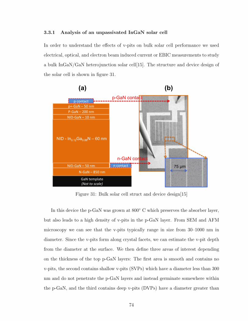
3.3.1 Analysis of an unpassivated InGaN solar cell
In order to understand the e↵ects of v-pits on bulk solar cell performance we used
electrical, optical, and electron beam induced current or EBIC measurements to study
a bulk InGaN/GaN heterojunction solar cell[15]. The structure and device design of
the solar cell is shown in figure 31.
GaNtemplate(Nottoscale)
N-GaN–850nm
P-GaN–200nmNID-GaN–10nm
NID - In0.12Ga0.88N – 60 nm
(a)
p+-GaN–50nm
NID-GaN–50nm
(b)
75 µm
pcontact
ncontact
p-GaN contact
n-GaN contact
Figure 31: Bulk solar cell struct and device design[15]
In this device the p-GaN was grown at 800� C which preserves the absorber layer,
but also leads to a high density of v-pits in the p-GaN layer. From SEM and AFM
microscopy we can see that the v-pits typically range in size from 30–1000 nm in
diameter. Since the v-pits form along crystal facets, we can estimate the v-pit depth
from the diameter at the surface. We then define three areas of interest depending
on the thickness of the top p-GaN layers: The first area is smooth and contains no
v-pits, the second contains shallow v-pits (SVPs) which have a diameter less than 300
nm and do not penetrate the p-GaN layers and instead germinate somewhere within
the p-GaN, and the third contains deep v-pits (DVPs) have a diameter greater than
74
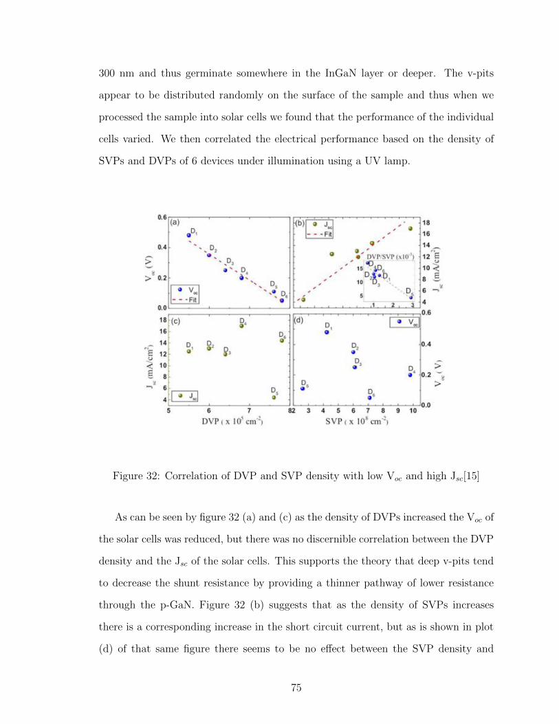
300 nm and thus germinate somewhere in the InGaN layer or deeper. The v-pits
appear to be distributed randomly on the surface of the sample and thus when we
processed the sample into solar cells we found that the performance of the individual
cells varied. We then correlated the electrical performance based on the density of
SVPs and DVPs of 6 devices under illumination using a UV lamp.
Figure 32: Correlation of DVP and SVP density with low Voc and high Jsc[15]
As can be seen by figure 32 (a) and (c) as the density of DVPs increased the Voc of
the solar cells was reduced, but there was no discernible correlation between the DVP
density and the Jsc of the solar cells. This supports the theory that deep v-pits tend
to decrease the shunt resistance by providing a thinner pathway of lower resistance
through the p-GaN. Figure 32 (b) suggests that as the density of SVPs increases
there is a corresponding increase in the short circuit current, but as is shown in plot
(d) of that same figure there seems to be no e↵ect between the SVP density and
75
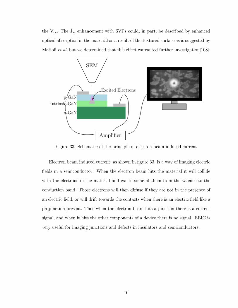
the Voc. The Jsc enhancement with SVPs could, in part, be described by enhanced
optical absorption in the material as a result of the textured surface as is suggested by
Matioli et al, but we determined that this e↵ect warranted further investigation[108].
Figure 33: Schematic of the principle of electron beam induced current
Electron beam induced current, as shown in figure 33, is a way of imaging electric
fields in a semiconductor. When the electron beam hits the material it will collide
with the electrons in the material and excite some of them from the valence to the
conduction band. Those electrons will then di↵use if they are not in the presence of
an electric field, or will drift towards the contacts when there is an electric field like a
pn junction present. Thus when the electron beam hits a junction there is a current
signal, and when it hits the other components of a device there is no signal. EBIC is
very useful for imaging junctions and defects in insulators and semiconductors.
76
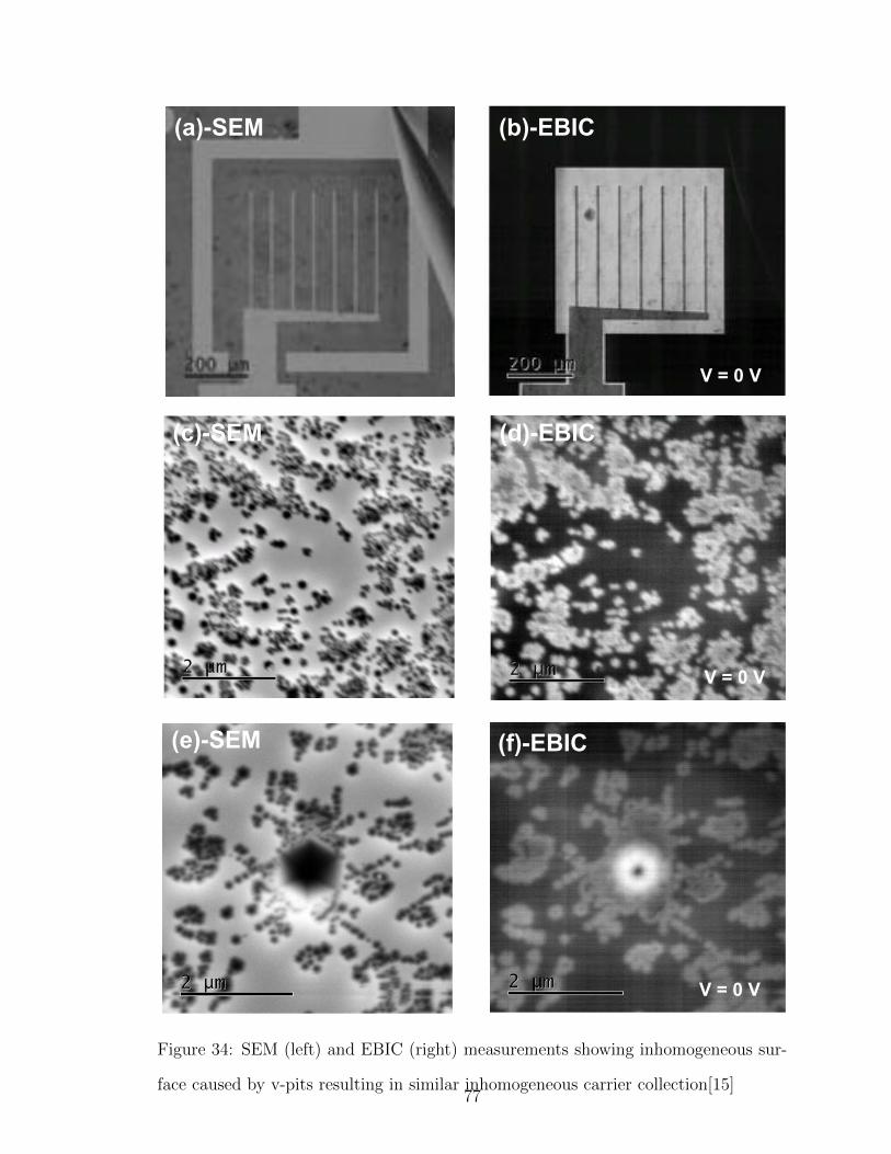
(a)-SEM
V = 0 V
(b)-EBIC
(c)-SEM (d)-EBIC
(e)-SEM (f)-EBIC
V = 0 V
V = 0 V
Figure 34: SEM (left) and EBIC (right) measurements showing inhomogeneous sur-
face caused by v-pits resulting in similar inhomogeneous carrier collection[15]77

In our case we can vary the depth of the penetration of the electron beam by
changing the accelerating voltage of the SEM. When the signal is bright, that means
that electrons are being collected from that region of the solar cell, but when the
signal is dark there is no carrier collection. This can parallel carrier collection that is
generated by exposure to solar radiation. As can be seen in figure 34 (e) and (f), the
center of the deep v-pit shows no collection. This is what is expected if the v-pit serves
as a channel for by-passing the junction and is consistent with our interpretation of
figure 32 (a). There is another interesting phenomenon present in figures 32 and 34,
and that is the e↵ect of the edges of the VPs, especially the SVPs on carrier collection.
As is clear from figure 34 (d) the SVPs show an enhanced EBIC signal in com-
parison to the smooth areas that contain no v-pits. In figure 34 (f) there is an
enhancement in collection from the edges of the v-pit even while the center is dark.
This is evidence that the enhanced short circuit current of “rough” InGaN solar cells
is a result of extra carrier collection as due to the presence of v-pits and not only
due to better light-trapping. There is a strain-field associated with the formation
of v-pits and this could act as a trap for impurities and defects, or indeed for the
dopant atoms, which are themselves substitutional impurities[135, 136]. Furthermore
GaN films have a high concentration of nitrogen vacancies (VN) which act as com-
pensating centers for the Mg, p-type doping and could be accommodated by the
v-pits[137, 138, 139, 140]. All of these lead to an enhancement of the space-charge
region around the v-pits which would increase carrier collection as demonstrated by
the EBIC results and an enhanced short-circuit current in InGaN solar cells with a
high density of v-pits.
3.3.2 Passivation of v-pits
Since the incorporation of v-pits seems to benefit the short-circuit current of InGaN
bases solar cells, but degrades the Voc an attempt was made to fill the v-pits with an
78
insulating material. Thus we sought to maintain their beneficial qualities to Jsc while
increasing the resistance of the leakage pathway. The process settled upon was to
use a spin on glass followed by etching. The thought was that after spin coating and
curing a spin on glass could recover the film’s smoothness. This smoothness would
then assist during the etching step by carefully etching down to the surface of the
p-GaN but leaving the glass in side the v-pits. Hydrogen silsesquioxane (HSQ) was
chosen as the spin on glass because of its low viscosity was believed to aide in the
filling of the v-pits, and because it was readily available.
HSQ is commercially available from DOW-Corning in a suspension that is either
1, 2, or 6%. The higher the percent of solid material the higher the viscosity and thus
the thicker the resulting film. The chemical formula for HSQ can be written HSiO3/2.
HSQ is typically used as a negative tone resist for electron beam lithography as
exposure to radiation tends to cause cross-linking which makes the film more di�cult
to remove in basic solution. There is also literature on the properties and use of
cured HSQ as a spin-on glass[16, 17, ?, 141]. In this case instead of cross-linking the
resist using electron radiation various chemical reactions are promoted by annealing
at di↵erent temperatures. Yang, et al break the annealing and chemical regimes into
4: room temperature–250� C, 250–350� C, 350–435� C, and > 435� C [?]. In the
first regime the solvent is removed. In the second regime, 250–350� C, the following
chemical reactions are promoted:
2 HSiO3/2
��! H2
SiO2/2
+ SiO4/2
H2
SiO2/2
+ HSiO3/2
��! SiO4/2
+ H3
SiO1/2
H3
SiO1/2
+ HSiO3/2
��! SiO4/2
+ SiH4
Then in regime 3, 350–435� C Si-H thermal disassociation and network redistribution
occur:
4 HSiO3/2
��! 3 SiO4/2
+ SiH4
79
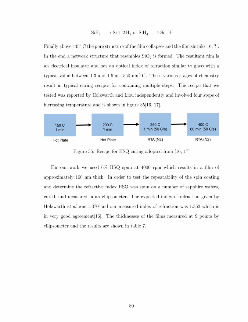
SiH4
��! Si + 2 H2
or SiH4
��! Si�H
Finally above 435� C the pore structure of the film collapses and the film shrinks[16, ?].
In the end a network structure that resembles SiO2
is formed. The resultant film is
an electrical insulator and has an optical index of refraction similar to glass with a
typical value between 1.3 and 1.6 at 1550 nm[16]. These various stages of chemistry
result in typical curing recipes for containing multiple steps. The recipe that we
tested was reported by Holzwarth and Liou independently and involved four steps of
increasing temperature and is shown in figure 35[16, 17].
Figure 35: Recipe for HSQ curing adopted from [16, 17]
For our work we used 6% HSQ spun at 4000 rpm which results in a film of
approximately 100 nm thick. In order to test the repeatability of the spin coating
and determine the refractive index HSQ was spun on a number of sapphire wafers,
cured, and measured in an ellipsometer. The expected index of refraction given by
Holzwarth et al was 1.370 and our measured index of refraction was 1.353 which is
in very good agreement[16]. The thicknesses of the films measured at 9 points by
ellipsometer and the results are shown in table 7.
80
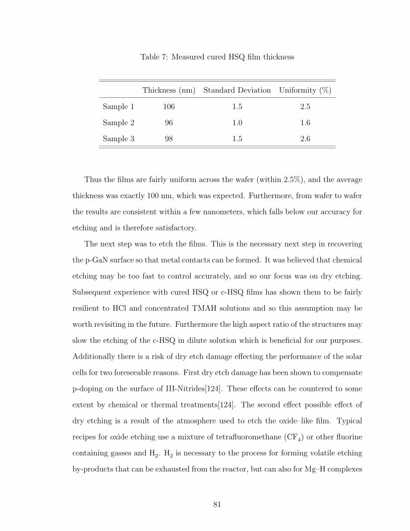
Table 7: Measured cured HSQ film thickness
Thickness (nm) Standard Deviation Uniformity (%)
Sample 1 106 1.5 2.5
Sample 2 96 1.0 1.6
Sample 3 98 1.5 2.6
Thus the films are fairly uniform across the wafer (within 2.5%), and the average
thickness was exactly 100 nm, which was expected. Furthermore, from wafer to wafer
the results are consistent within a few nanometers, which falls below our accuracy for
etching and is therefore satisfactory.
The next step was to etch the films. This is the necessary next step in recovering
the p-GaN surface so that metal contacts can be formed. It was believed that chemical
etching may be too fast to control accurately, and so our focus was on dry etching.
Subsequent experience with cured HSQ or c-HSQ films has shown them to be fairly
resilient to HCl and concentrated TMAH solutions and so this assumption may be
worth revisiting in the future. Furthermore the high aspect ratio of the structures may
slow the etching of the c-HSQ in dilute solution which is beneficial for our purposes.
Additionally there is a risk of dry etch damage e↵ecting the performance of the solar
cells for two foreseeable reasons. First dry etch damage has been shown to compensate
p-doping on the surface of III-Nitrides[124]. These e↵ects can be countered to some
extent by chemical or thermal treatments[124]. The second e↵ect possible e↵ect of
dry etching is a result of the atmosphere used to etch the oxide–like film. Typical
recipes for oxide etching use a mixture of tetrafluoromethane (CF4
) or other fluorine
containing gasses and H2
. H2
is necessary to the process for forming volatile etching
by-products that can be exhausted from the reactor, but can also for Mg–H complexes
81
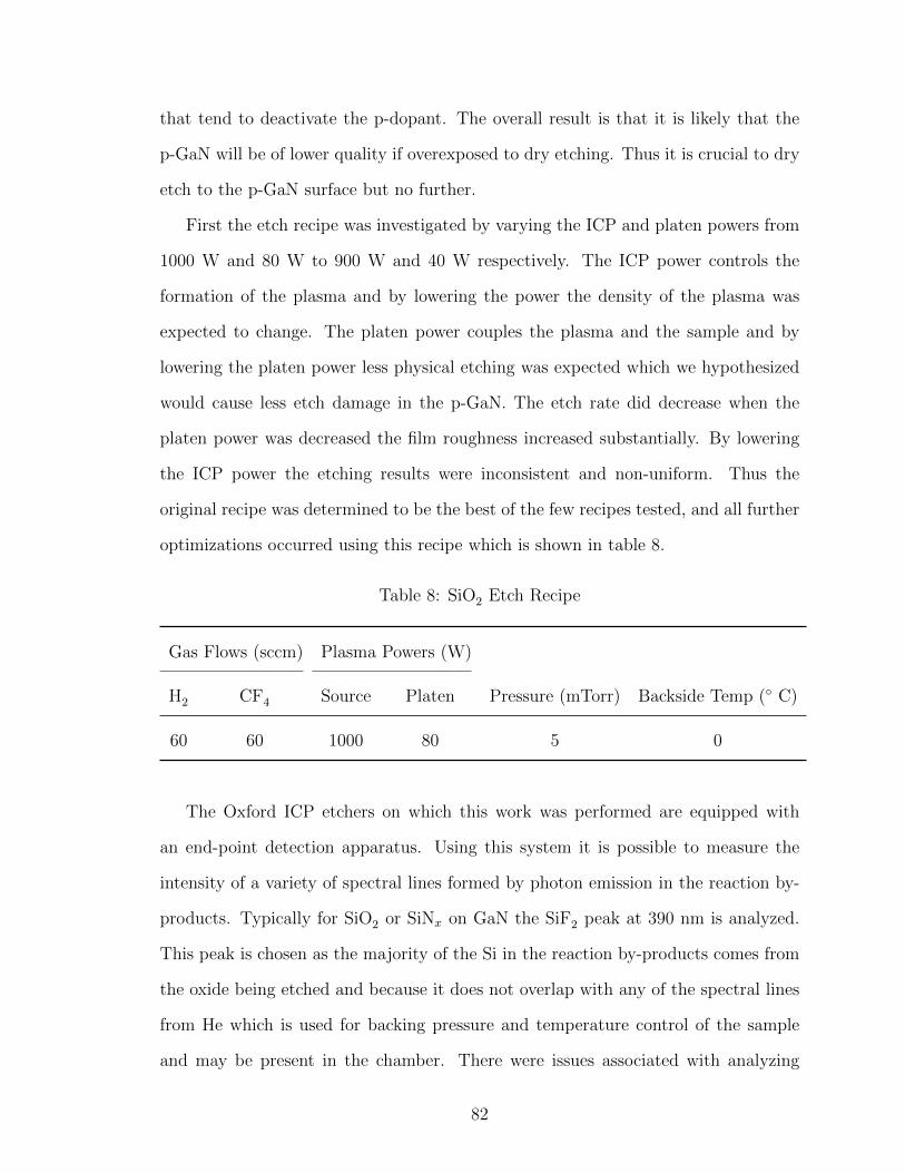
that tend to deactivate the p-dopant. The overall result is that it is likely that the
p-GaN will be of lower quality if overexposed to dry etching. Thus it is crucial to dry
etch to the p-GaN surface but no further.
First the etch recipe was investigated by varying the ICP and platen powers from
1000 W and 80 W to 900 W and 40 W respectively. The ICP power controls the
formation of the plasma and by lowering the power the density of the plasma was
expected to change. The platen power couples the plasma and the sample and by
lowering the platen power less physical etching was expected which we hypothesized
would cause less etch damage in the p-GaN. The etch rate did decrease when the
platen power was decreased the film roughness increased substantially. By lowering
the ICP power the etching results were inconsistent and non-uniform. Thus the
original recipe was determined to be the best of the few recipes tested, and all further
optimizations occurred using this recipe which is shown in table 8.
Table 8: SiO2
Etch Recipe
Gas Flows (sccm) Plasma Powers (W)
H2
CF4
Source Platen Pressure (mTorr) Backside Temp (� C)
60 60 1000 80 5 0
The Oxford ICP etchers on which this work was performed are equipped with
an end-point detection apparatus. Using this system it is possible to measure the
intensity of a variety of spectral lines formed by photon emission in the reaction by-
products. Typically for SiO2
or SiNx on GaN the SiF2
peak at 390 nm is analyzed.
This peak is chosen as the majority of the Si in the reaction by-products comes from
the oxide being etched and because it does not overlap with any of the spectral lines
from He which is used for backing pressure and temperature control of the sample
and may be present in the chamber. There were issues associated with analyzing
82
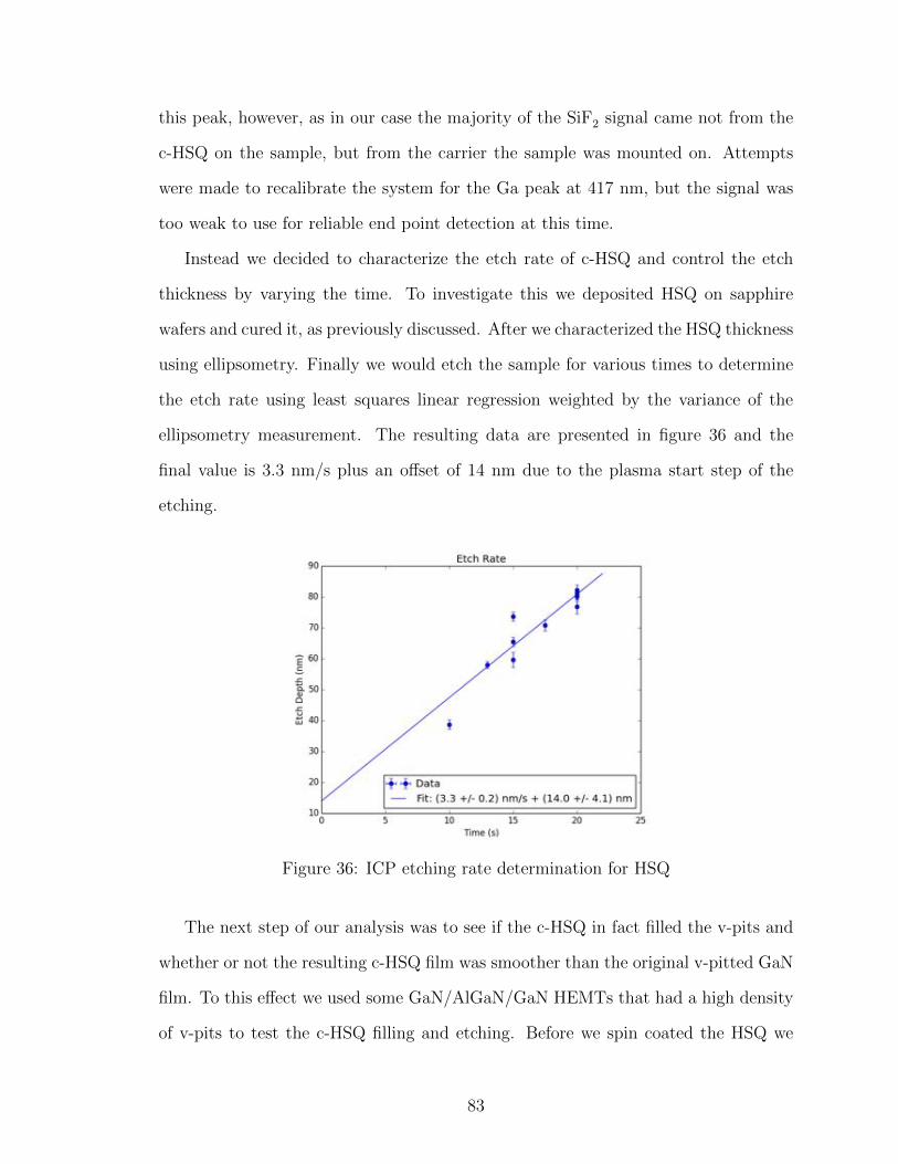
this peak, however, as in our case the majority of the SiF2
signal came not from the
c-HSQ on the sample, but from the carrier the sample was mounted on. Attempts
were made to recalibrate the system for the Ga peak at 417 nm, but the signal was
too weak to use for reliable end point detection at this time.
Instead we decided to characterize the etch rate of c-HSQ and control the etch
thickness by varying the time. To investigate this we deposited HSQ on sapphire
wafers and cured it, as previously discussed. After we characterized the HSQ thickness
using ellipsometry. Finally we would etch the sample for various times to determine
the etch rate using least squares linear regression weighted by the variance of the
ellipsometry measurement. The resulting data are presented in figure 36 and the
final value is 3.3 nm/s plus an o↵set of 14 nm due to the plasma start step of the
etching.
Figure 36: ICP etching rate determination for HSQ
The next step of our analysis was to see if the c-HSQ in fact filled the v-pits and
whether or not the resulting c-HSQ film was smoother than the original v-pitted GaN
film. To this e↵ect we used some GaN/AlGaN/GaN HEMTs that had a high density
of v-pits to test the c-HSQ filling and etching. Before we spin coated the HSQ we
83
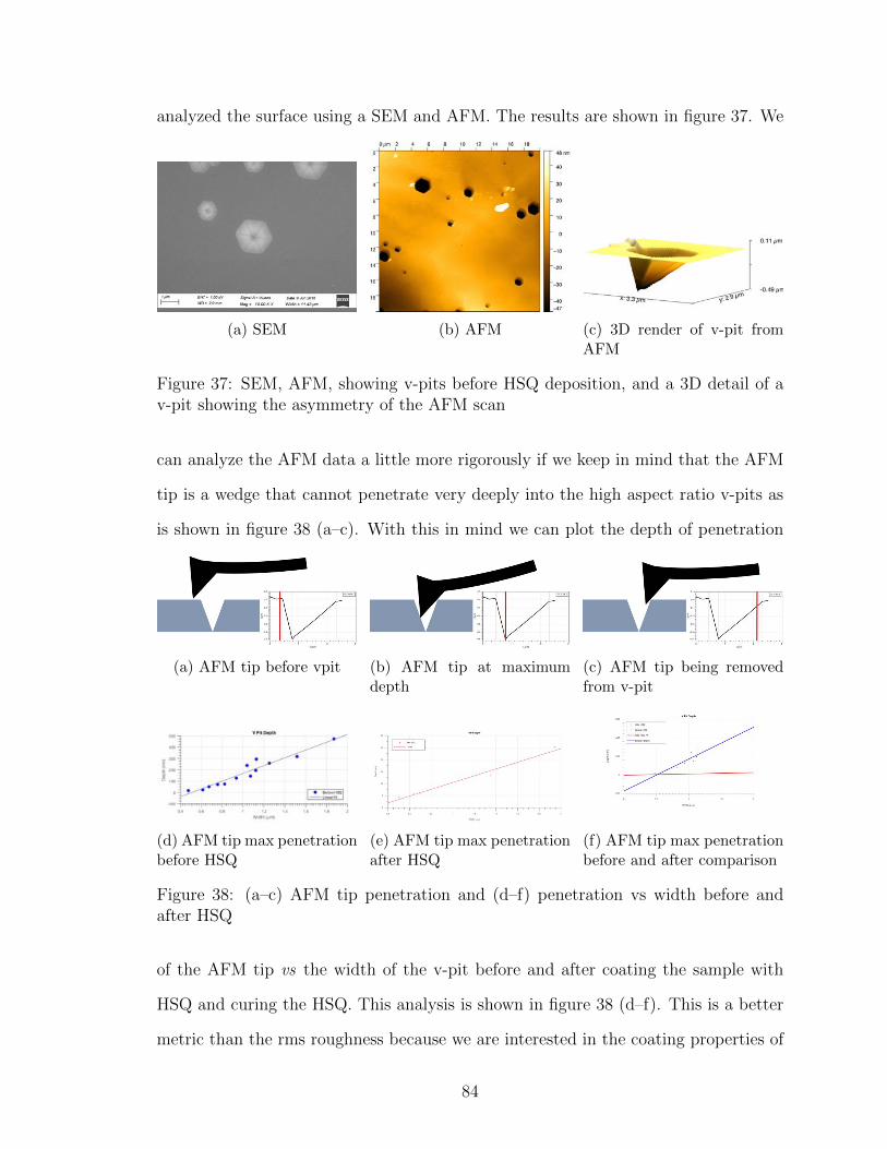
analyzed the surface using a SEM and AFM. The results are shown in figure 37. We
(a) SEM (b) AFM (c) 3D render of v-pit fromAFM
Figure 37: SEM, AFM, showing v-pits before HSQ deposition, and a 3D detail of av-pit showing the asymmetry of the AFM scan
can analyze the AFM data a little more rigorously if we keep in mind that the AFM
tip is a wedge that cannot penetrate very deeply into the high aspect ratio v-pits as
is shown in figure 38 (a–c). With this in mind we can plot the depth of penetration
(a) AFM tip before vpit (b) AFM tip at maximumdepth
(c) AFM tip being removedfrom v-pit
(d) AFM tip max penetrationbefore HSQ
(e) AFM tip max penetrationafter HSQ
(f) AFM tip max penetrationbefore and after comparison
Figure 38: (a–c) AFM tip penetration and (d–f) penetration vs width before andafter HSQ
of the AFM tip vs the width of the v-pit before and after coating the sample with
HSQ and curing the HSQ. This analysis is shown in figure 38 (d–f). This is a better
metric than the rms roughness because we are interested in the coating properties of
84
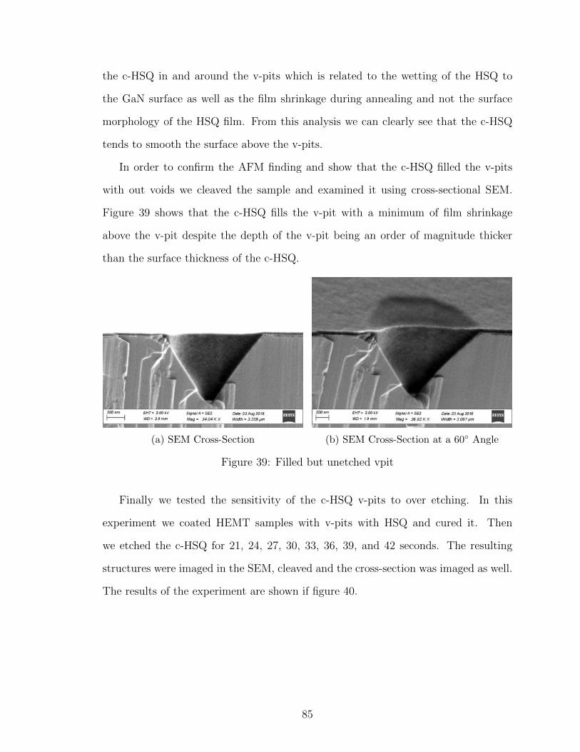
the c-HSQ in and around the v-pits which is related to the wetting of the HSQ to
the GaN surface as well as the film shrinkage during annealing and not the surface
morphology of the HSQ film. From this analysis we can clearly see that the c-HSQ
tends to smooth the surface above the v-pits.
In order to confirm the AFM finding and show that the c-HSQ filled the v-pits
with out voids we cleaved the sample and examined it using cross-sectional SEM.
Figure 39 shows that the c-HSQ fills the v-pit with a minimum of film shrinkage
above the v-pit despite the depth of the v-pit being an order of magnitude thicker
than the surface thickness of the c-HSQ.
(a) SEM Cross-Section (b) SEM Cross-Section at a 60� Angle
Figure 39: Filled but unetched vpit
Finally we tested the sensitivity of the c-HSQ v-pits to over etching. In this
experiment we coated HEMT samples with v-pits with HSQ and cured it. Then
we etched the c-HSQ for 21, 24, 27, 30, 33, 36, 39, and 42 seconds. The resulting
structures were imaged in the SEM, cleaved and the cross-section was imaged as well.
The results of the experiment are shown if figure 40.
85
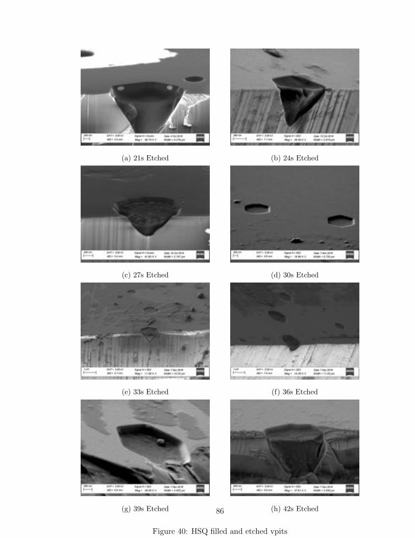
(a) 21s Etched (b) 24s Etched
(c) 27s Etched (d) 30s Etched
(e) 33s Etched (f) 36s Etched
(g) 39s Etched (h) 42s Etched
Figure 40: HSQ filled and etched vpits
86
It is clear from the images that the HSQ is etched on the surface and inside the
v-pit to some extent, but etching in the v-pits seems to be fairly resilient as there is
very little di↵erence between 21 and 42s of etching. Furthermore the process more
repeatable because the c-HSQ is only 100 nm thick on the surface and the v-pits that
need to be masked are often twice as thick.
3.4 Metal–Gan Contacts
We address the work done on metal contacting of GaN. Since solar cells and LEDs are
both PIN diode structures n-type and p-type contacts are required. N-type metal–
semiconductor ohmic contact formation in GaN has not posed much of a problem.
Typically low work function metals are used, and wide variety of metals can make
ohmic, n-type contact to GaN. Metal to p-GaN ohmic contacts have been more di�-
cult to achieve. Firstly high work function metals are required because GaN is a wide
band gap semiconductor, and this narrows the selection of metals significantly. This
is further compounded by the di�culty of p-doping GaN.
We investigate a variety of contacting schemes as well as recipes for achieving
high quality metal–GaN contacts. Of chief concern is the resistance of the contacts in
⌦s. A high contact resistance leads to a high series resistance for the solar cell and a
degradation of the e�ciency. This quantity is typically characterized by the specific
contact resistivity, ⇢c, which is independent of the contact geometry and has units of
⌦· cm2. The specific contact resistivity is equivalent to the change in voltage divided
by the current density or:
pc =
✓@J
@V
◆�1
V =0
(42)
The various factors associated with specific contact resistivity are discussed below
and several contacting schemes were investigated for both n and p-type GaN.
87
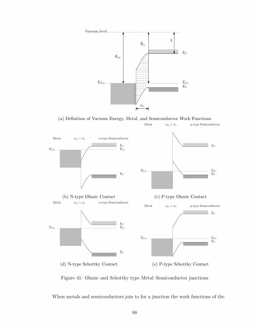
EFm
EC
EV
EFs
Vacuum level
�m
�s
�
++++++++++
����������������
���������������
���������������
���������������
��������������
���������������
W0
(a) Definition of Vacuum Energy, Metal, and Semiconductor Work Functions
EFm
EC
EV
n-type SemiconductorMetal �m
< �s
EFs
(b) N-type Ohmic Contact
EFm
EC
EV
p-type SemiconductorMetal �m
> �s
EFs
(c) P-type Ohmic Contact
EFm
EC
EV
n-type SemiconductorMetal �m
> �s
EFs
(d) N-type Schottky Contact
EFm
EC
EV
p-type SemiconductorMetal �m
< �s
EFs
(e) P-type Schottky Contact
Figure 41: Ohmic and Schottky type Metal–Semiconductor junctions
When metals and semiconductors join to for a junction the work functions of the
88
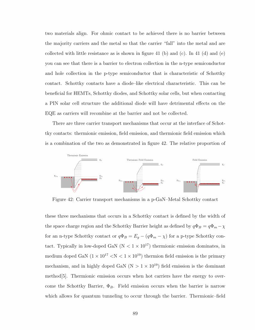
two materials align. For ohmic contact to be achieved there is no barrier between
the majority carriers and the metal so that the carrier “fall” into the metal and are
collected with little resistance as is shown in figure 41 (b) and (c). In 41 (d) and (e)
you can see that there is a barrier to electron collection in the n-type semiconductor
and hole collection in the p-type semiconductor that is characteristic of Schottky
contact. Schottky contacts have a diode–like electrical characteristic. This can be
beneficial for HEMTs, Schottky diodes, and Schottky solar cells, but when contacting
a PIN solar cell structure the additional diode will have detrimental e↵ects on the
EQE as carriers will recombine at the barrier and not be collected.
There are three carrier transport mechanisms that occur at the interface of Schot-
tky contacts: thermionic emission, field emission, and thermionic field emission which
is a combination of the two as demonstrated in figure 42. The relative proportion of
EFm
EC
EV
EFs
++++++++++
����������������
���������������
���������������
���������������
��������������
���������������
Thermionic Emission
EFm
EC
EV
EFs
++++++++++
���������������
��������������
�������������
��������������
�������������
Thermionic Field Emission
��
��
��
EFm
EC
EV
EFs
++++++++++
���������������
��������������
��
�����������
��
Field Emission
�
�
Figure 42: Carrier transport mechanisms in a p-GaN–Metal Schottky contact
these three mechanisms that occurs in a Schottky contact is defined by the width of
the space charge region and the Schottky Barrier height as defined by q�B = q�m��
for an n-type Schottky contact or q�B = Eg � (q�m � �) for a p-type Schottky con-
tact. Typically in low-doped GaN (N < 1 ⇥ 1017) thermionic emission dominates, in
medium doped GaN (1⇥ 1017 <N < 1⇥ 1019) thermion field emission is the primary
mechanism, and in highly doped GaN (N > 1 ⇥ 1019) field emission is the dominant
method[5]. Thermionic emission occurs when hot carriers have the energy to over-
come the Schottky Barrier, �B. Field emission occurs when the barrier is narrow
which allows for quantum tunneling to occur through the barrier. Thermionic–field
89
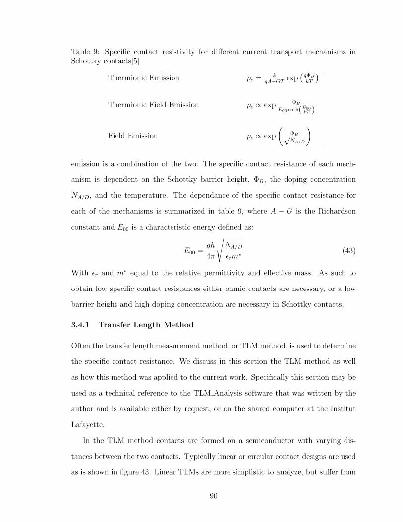
Table 9: Specific contact resistivity for di↵erent current transport mechanisms inSchottky contacts[5]
Thermionic Emission ⇢c = kqA�GT
exp�q�
B
kT
�
Thermionic Field Emission ⇢c / exp �
B
E00
coth(E
00
kT
)
Field Emission ⇢c / exp
✓�
BpN
A/D
◆
emission is a combination of the two. The specific contact resistance of each mech-
anism is dependent on the Schottky barrier height, �B, the doping concentration
NA/D, and the temperature. The dependance of the specific contact resistance for
each of the mechanisms is summarized in table 9, where A � G is the Richardson
constant and E00
is a characteristic energy defined as:
E00
=qh
4⇡
sNA/D
✏rm⇤ (43)
With ✏r and m⇤ equal to the relative permittivity and e↵ective mass. As such to
obtain low specific contact resistances either ohmic contacts are necessary, or a low
barrier height and high doping concentration are necessary in Schottky contacts.
3.4.1 Transfer Length Method
Often the transfer length measurement method, or TLM method, is used to determine
the specific contact resistance. We discuss in this section the TLM method as well
as how this method was applied to the current work. Specifically this section may be
used as a technical reference to the TLM Analysis software that was written by the
author and is available either by request, or on the shared computer at the Institut
Lafayette.
In the TLM method contacts are formed on a semiconductor with varying dis-
tances between the two contacts. Typically linear or circular contact designs are used
as is shown in figure 43. Linear TLMs are more simplistic to analyze, but su↵er from
90
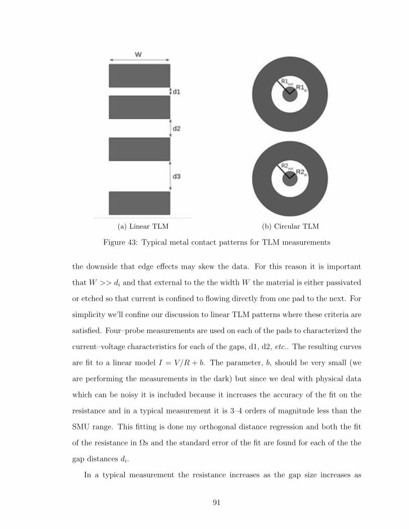
(a) Linear TLM (b) Circular TLM
Figure 43: Typical metal contact patterns for TLM measurements
the downside that edge e↵ects may skew the data. For this reason it is important
that W >> di and that external to the the width W the material is either passivated
or etched so that current is confined to flowing directly from one pad to the next. For
simplicity we’ll confine our discussion to linear TLM patterns where these criteria are
satisfied. Four–probe measurements are used on each of the pads to characterized the
current–voltage characteristics for each of the gaps, d1, d2, etc.. The resulting curves
are fit to a linear model I = V/R + b. The parameter, b, should be very small (we
are performing the measurements in the dark) but since we deal with physical data
which can be noisy it is included because it increases the accuracy of the fit on the
resistance and in a typical measurement it is 3–4 orders of magnitude less than the
SMU range. This fitting is done my orthogonal distance regression and both the fit
of the resistance in ⌦s and the standard error of the fit are found for each of the the
gap distances di.
In a typical measurement the resistance increases as the gap size increases as
91
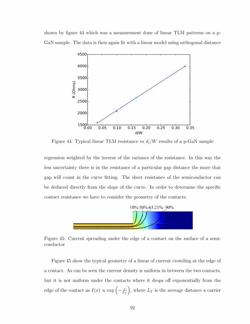
shown by figure 44 which was a measurement done of linear TLM patterns on a p-
GaN sample. The data is then again fit with a linear model using orthogonal distance
Figure 44: Typical linear TLM resistance vs di/W results of a p-GaN sample
regression weighted by the inverse of the variance of the resistance. In this way the
less uncertainty there is in the resistance of a particular gap distance the more that
gap will count in the curve fitting. The sheet resistance of the semiconductor can
be deduced directly from the slope of the curve. In order to determine the specific
contact resistance we have to consider the geometry of the contacts.
Figure 45: Current spreading under the edge of a contact on the surface of a semi-conductor
Figure 45 show the typical geometry of a linear of current crowding at the edge of
a contact. As can be seen the current density is uniform in between the two contacts,
but it is not uniform under the contacts where it drops o↵ exponentially from the
edge of the contact as I(x) / exp⇣� x
LT
⌘, where LT is the average distance a carrier
92
travels under the contact before it is collected by the contact and is called the transfer
length. Thus the e↵ective contact area is W ⇥LT , and we can write the resistance as
a function of d the gap between two contacts as:
R(d) =Rsh
Wd + 2
RshLT
W(44)
We can also determine the specific contact resistance:
⇢c = L2
TRsh (45)
The results for Rsh, LT , and ⇢c are then obtained from the linear fit and the
associated uncertainties from the standard errors of the fit. Analogously for circular
TLM patterns we can write the total resistance as a function of the inner and outer
radii as such:
R =Rsh
2⇡
✓ln
Rout
Rin
+ LT
✓1
Rout
+1
Rin
◆◆(46)
If all of the inner radii are equal we can further parameterize this equation by the
gap between the inner and outer raddi, d:
R(d) =Rsh
2⇡
✓ln
Rin+d
Rin
+ LT
✓1
Rin+d
+1
Rin
◆◆(47)
This equation can easily be fit using non-linear regression methods like orthogonal
distance regression. If both of the inner and outer radii vary however regression be-
comes di�cult. Furthermore the experiment becomes more of a practical challenge
as intuition is lost as to whether one gap size should have a higher or lower resistance
than a previous gap size and experimental errors are more common. However we can
parameterize the general equation by defining A = 1
2⇡ln R
out
Rin
and B = 1
2⇡
⇣1
Rout
+ 1
Rin
⌘
which depend on the known radii. Then we can rearrange to discover a linear rela-
tionship vs B/A:
R
A(B/A) = Rsh (1 + LT (B/A)) (48)
We can then find the values of Rsh, LT , and ⇢c by plotting RAvs B/A.
93
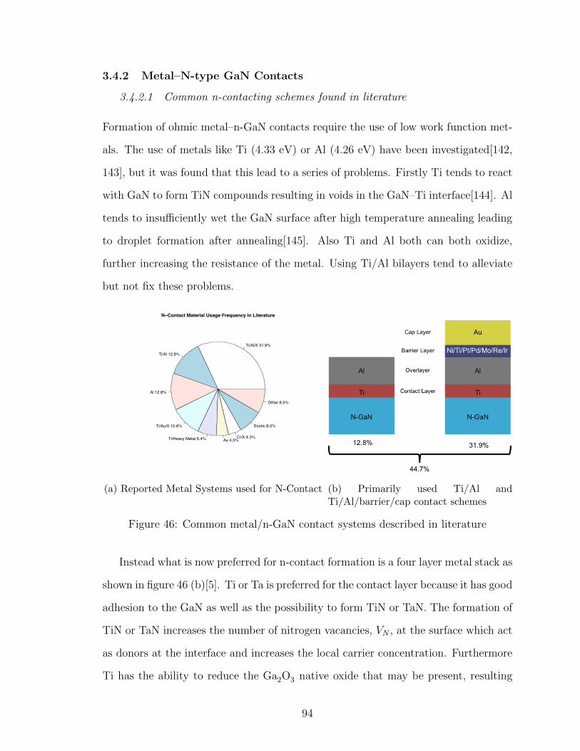
3.4.2 Metal–N-type GaN Contacts
3.4.2.1 Common n-contacting schemes found in literature
Formation of ohmic metal–n-GaN contacts require the use of low work function met-
als. The use of metals like Ti (4.33 eV) or Al (4.26 eV) have been investigated[142,
143], but it was found that this lead to a series of problems. Firstly Ti tends to react
with GaN to form TiN compounds resulting in voids in the GaN–Ti interface[144]. Al
tends to insu�ciently wet the GaN surface after high temperature annealing leading
to droplet formation after annealing[145]. Also Ti and Al both can both oxidize,
further increasing the resistance of the metal. Using Ti/Al bilayers tend to alleviate
but not fix these problems.
Ti/Al/X 31.9%
Ti/Al 12.8%
Al 12.8%
Ti/Au/X 10.6%
Ti/Heavy Metal 6.4% Au 4.3%Cr/X 4.3%
Exotic 8.5%
Other 8.5%
N−Contact Material Usage Frequency in Literature
(a) Reported Metal Systems used for N-Contact (b) Primarily used Ti/Al andTi/Al/barrier/cap contact schemes
Figure 46: Common metal/n-GaN contact systems described in literature
Instead what is now preferred for n-contact formation is a four layer metal stack as
shown in figure 46 (b)[5]. Ti or Ta is preferred for the contact layer because it has good
adhesion to the GaN as well as the possibility to form TiN or TaN. The formation of
TiN or TaN increases the number of nitrogen vacancies, VN , at the surface which act
as donors at the interface and increases the local carrier concentration. Furthermore
Ti has the ability to reduce the Ga2
O3
native oxide that may be present, resulting
94
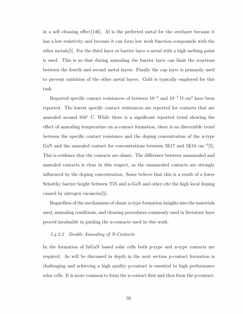
in a self–cleaning e↵ect[146]. Al is the preferred metal for the overlayer because it
has a low resistivity and because it can form low work function compounds with the
other metals[5]. For the third layer or barrier layer a metal with a high melting point
is used. This is so that during annealing the barrier layer can limit the reactions
between the fourth and second metal layers. Finally the cap layer is primarily used
to prevent oxidation of the other metal layers. Gold is typically employed for this
task.
Reported specific contact resistances of between 10�2 and 10�7 ⌦ cm2 have been
reported. The lowest specific contact resistances are reported for contacts that are
annealed around 850� C. While there is a significant reported trend showing the
e↵ect of annealing temperature on n-contact formation, there is no discernible trend
between the specific contact resistance and the doping concentration of the n-type
GaN and the annealed contact for concentrations between 5E17 and 5E18 cm�3[5].
This is evidence that the contacts are ohmic. The di↵erence between unannealed and
annealed contacts is clear in this respect, as the unannealed contacts are strongly
influenced by the doping concentration. Some believe that this is a result of a lower
Schottky barrier height between TiN and n-GaN and other cite the high local doping
caused by nitrogen vacancies[5].
Regardless of the mechanisms of ohmic n-type formation insights into the materials
used, annealing conditions, and cleaning procedures commonly used in literature have
proved invaluable in guiding the n-contacts used in this work.
3.4.2.2 Double Annealing of N-Contacts
In the formation of InGaN based solar cells both p-type and n-type contacts are
required. As will be discussed in depth in the next section p-contact formation is
challenging and achieving a high quality p-contact is essential to high performance
solar cells. It is more common to form the n-contact first and then form the p-contact.
95
In this case the n-contact is made and annealed followed by p-contact formation and
annealing. Thus the n-contact is annealed twice. We have studied the e↵ect of double
annealing on three di↵erent n-contacting schemes on identical LED samples.
Figure 47: Ti/Al (20/20 nm) circular TLM contacts before and after annealing at
The first n-contact scheme investigated was to use Ti/Al (20/20 nm), annealed
under nitrogen for ohmic n-contact formation and then annealed again under oxygen,
this time for the ohmic p-contact formation. After the p-contact was formed the same
bus bar would be deposited on both the p and n contacts. This bus bar consisted of
Ni/Al/Ni/Au (25/200/25/25 nm). The Ni/Al/Ni/Au stack was supposed to have a
low resistance as well as interface well with both the p-contact (Ni/Au) and the n-
contact (Ti/Al). Figure 47 shows the e↵ect of 60s annealing at 850� C under nitrogen
atmosphere on the current–voltage characteristics of the contacts. As can be seen the
resistance decreases significantly and the contacts go from having a Schottky behavior
to displaying ohmic characteristics. However the surface morphology of the contacts
96
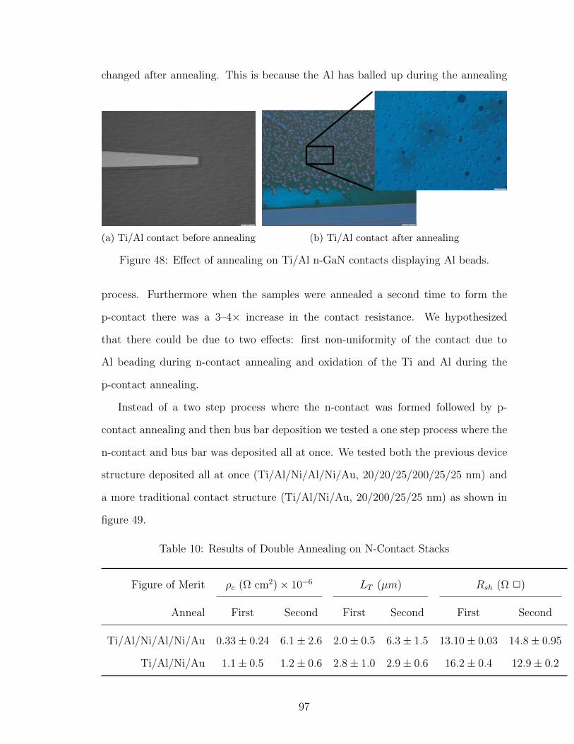
changed after annealing. This is because the Al has balled up during the annealing
(a) Ti/Al contact before annealing (b) Ti/Al contact after annealing
Figure 48: E↵ect of annealing on Ti/Al n-GaN contacts displaying Al beads.
process. Furthermore when the samples were annealed a second time to form the
p-contact there was a 3–4⇥ increase in the contact resistance. We hypothesized
that there could be due to two e↵ects: first non-uniformity of the contact due to
Al beading during n-contact annealing and oxidation of the Ti and Al during the
p-contact annealing.
Instead of a two step process where the n-contact was formed followed by p-
contact annealing and then bus bar deposition we tested a one step process where the
n-contact and bus bar was deposited all at once. We tested both the previous device
structure deposited all at once (Ti/Al/Ni/Al/Ni/Au, 20/20/25/200/25/25 nm) and
a more traditional contact structure (Ti/Al/Ni/Au, 20/200/25/25 nm) as shown in
figure 49.
Table 10: Results of Double Annealing on N-Contact Stacks
Figure of Merit ⇢c (⌦ cm2) ⇥ 10�6 LT (µm) Rsh (⌦ 2)
Anneal First Second First Second First Second
Ti/Al/Ni/Al/Ni/Au 0.33 ± 0.24 6.1 ± 2.6 2.0 ± 0.5 6.3 ± 1.5 13.10 ± 0.03 14.8 ± 0.95
Ti/Al/Ni/Au 1.1 ± 0.5 1.2 ± 0.6 2.8 ± 1.0 2.9 ± 0.6 16.2 ± 0.4 12.9 ± 0.2
97
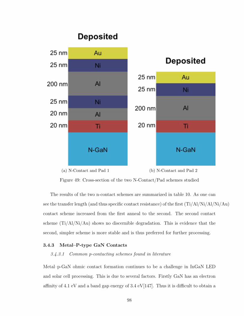
(a) N-Contact and Pad 1 (b) N-Contact and Pad 2
Figure 49: Cross-section of the two N-Contact/Pad schemes studied
The results of the two n-contact schemes are summarized in table 10. As one can
see the transfer length (and thus specific contact resistance) of the first (Ti/Al/Ni/Al/Ni/Au)
contact scheme increased from the first anneal to the second. The second contact
scheme (Ti/Al/Ni/Au) shows no discernible degradation. This is evidence that the
second, simpler scheme is more stable and is thus preferred for further processing.
3.4.3 Metal–P-type GaN Contacts
3.4.3.1 Common p-contacting schemes found in literature
Metal–p-GaN ohmic contact formation continues to be a challenge in InGaN LED
and solar cell processing. This is due to several factors. Firstly GaN has an electron
a�nity of 4.1 eV and a band gap energy of 3.4 eV[147]. Thus it is di�cult to obtain a
98
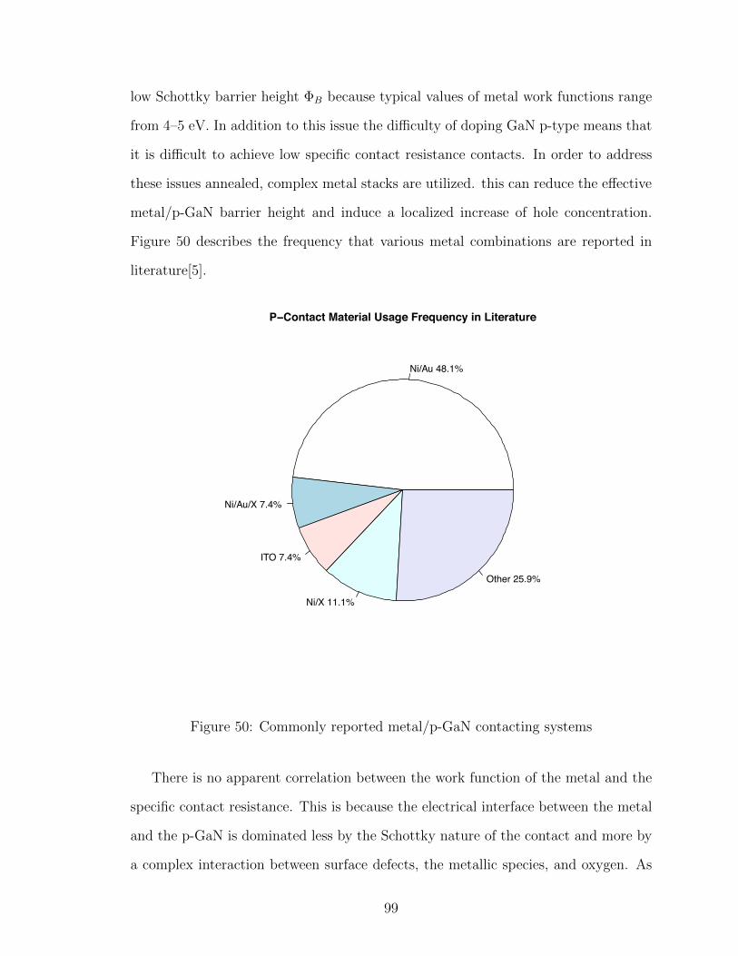
low Schottky barrier height �B because typical values of metal work functions range
from 4–5 eV. In addition to this issue the di�culty of doping GaN p-type means that
it is di�cult to achieve low specific contact resistance contacts. In order to address
these issues annealed, complex metal stacks are utilized. this can reduce the e↵ective
metal/p-GaN barrier height and induce a localized increase of hole concentration.
Figure 50 describes the frequency that various metal combinations are reported in
literature[5].
Ni/Au 48.1%
Ni/Au/X 7.4%
ITO 7.4%
Ni/X 11.1%
Other 25.9%
P−Contact Material Usage Frequency in Literature
Figure 50: Commonly reported metal/p-GaN contacting systems
There is no apparent correlation between the work function of the metal and the
specific contact resistance. This is because the electrical interface between the metal
and the p-GaN is dominated less by the Schottky nature of the contact and more by
a complex interaction between surface defects, the metallic species, and oxygen. As
99
50 shows the most reported metal contacting scheme to p-GaN, by a large margin
is Ni/Au[5]. Furthermore, Ni/Au is the contact of choice for InGaN based solar
cells because annealed, thin (5/5 nm) Ni/Au layers are semitransparent allowing
transmission of up to 85% of incident light[122].
3.4.3.2 Ni/Au contact to p-GaN
One significant finding concerning Ni/Au contacts to p-GaN is that annealing the
contacts in an oxygen containing ambient tends to decrease the specific contact re-
sistance by an order of magnitude[5]. The role that oxygen plays in the formation
of ohmic contacts is not well understood, however. Leading hypotheses are that NiO
at the interface can be formed during annealing[148, 5, 149]. It has been reported
that the NiO and p-GaN can form a contact with a low Schottky barrier height (0.19
eV)[150], but the height of this barrier has been contested by other sources and re-
ported values as high as 2.28 eV[151]. The controversy about the Schottky barrier
height of NiO/p-GaN makes it impossible to know what role, if any, the presence of
NiO at the interface plays in the formation of ohmic contacts.
Another hypothesis about the role of oxygen in the formation of ohmic contacts
arrises from the Mg–H complexes that can form and tend to strongly decrease the
number of activated acceptors. This hypothesis states that during annealing with
oxygen the Mg–H complexes can be disassociated and the oxygen containing atmo-
sphere can reduce the hydrogen. This will increase the amount of free carriers in the
p-GaN film and narrow the width of the Schottky barrier. Hull el al. demonstrate
that an oxygen anneal does tend to decrease the amount of H contained in the p-GaN
film[greco 100]. However, our own analysis has shown by Hall e↵ect measurement
that before and after annealing in oxygen there is no change in the number of carriers
in the film. This is consistent with studies of contact annealing in Ar and N2
/O2
atmospheres performed by Greco et al. in which there was no change found in the
100

doping concentration of the two samples[152].
Furthermore the studies by Koide et al. and Greco et al. showed that there was a
decrease in Schottky barrier height for the sample annealed in N2
/O2
(0.6–0.78 eV)
compared to the sample annealed in N2
or Ar alone (1.07 eV)[152, 148]. This decrease
is consistent with the findings of Ishikawa et al. who found that the removal of a 2
nm insulator like the Ga2
O3
native oxide would change the Schottky barrier height
by 0.2–0.3 eV[153]. TEM and XRD analysis or Ni/Au contacts made to p-GaN that
have been annealed either in Ar or N2
/O2
ambient show that a Ni/Au solid solution as
well as a NiO layer are formed under oxygen[149]. Specifically, under Ar atmosphere
Figure 51: Schematic of TLM results on Ni/Au p-GaN contacts annealed in Ar (left)and N
2
/O2
(right)
there is a clear delineation between the Ni and Au layers after annealing. However
when the same contacts are annealed under N2
the Ni at the interface is no longer
present and the XRD data that Ni has reacted with O2
to form NiO on the surface
as displayed schematically in figure 51[149]. This results in an apparent inversion
sequence that has been referenced by several authors like Ishikawa et al.[153]. The
belief is that Ni on the surface of the contact can reduce the native oxide and then
di↵use into the Au contact resulting in a self-cleaning e↵ect. Other Ni will form a
solid solution with the Au layer and may out-di↵use and transform into NiO at the
surface. The resultant out di↵usion and NiO formation at the surface may be the
cause of the apparent inversion sequence[5, 154].
101
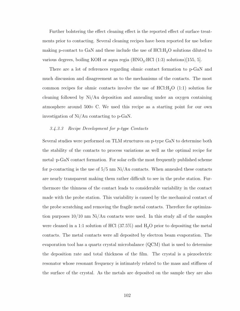
Further bolstering the e↵ect cleaning e↵ect is the reported e↵ect of surface treat-
ments prior to contacting. Several cleaning recipes have been reported for use before
making p-contact to GaN and these include the use of HCl:H2
O solutions diluted to
various degrees, boiling KOH or aqua regia (HNO3
:HCl (1:3) solutions)[155, 5].
There are a lot of references regarding ohmic contact formation to p-GaN and
much discussion and disagreement as to the mechanisms of the contacts. The most
common recipes for ohmic contacts involve the use of HCl:H2
O (1:1) solution for
cleaning followed by Ni/Au deposition and annealing under an oxygen containing
atmosphere around 500� C. We used this recipe as a starting point for our own
investigation of Ni/Au contacting to p-GaN.
3.4.3.3 Recipe Development for p-type Contacts
Several studies were performed on TLM structures on p-type GaN to determine both
the stability of the contacts to process variations as well as the optimal recipe for
metal–p-GaN contact formation. For solar cells the most frequently published scheme
for p-contacting is the use of 5/5 nm Ni/Au contacts. When annealed these contacts
are nearly transparent making them rather di�cult to see in the probe station. Fur-
thermore the thinness of the contact leads to considerable variability in the contact
made with the probe station. This variability is caused by the mechanical contact of
the probe scratching and removing the fragile metal contacts. Therefore for optimiza-
tion purposes 10/10 nm Ni/Au contacts were used. In this study all of the samples
were cleaned in a 1:1 solution of HCl (37.5%) and H2
O prior to depositing the metal
contacts. The metal contacts were all deposited by electron beam evaporation. The
evaporation tool has a quartz crystal microbalance (QCM) that is used to determine
the deposition rate and total thickness of the film. The crystal is a piezoelectric
resonator whose resonant frequency is intimately related to the mass and sti↵ness of
the surface of the crystal. As the metals are deposited on the sample they are also
102
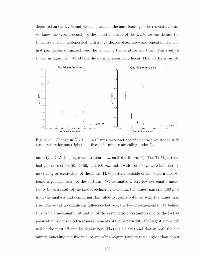
deposited on the QCM and we can determine the mass loading of the resonator. Since
we know the typical density of the metal and area of the QCM we can deduce the
thickness of the film deposited with a high degree of accuracy and repeatability. The
first parameters optimized were the annealing temperature and time. This study is
shown in figure 52. We obtain the data by measuring linear TLM patterns on 540
Figure 52: Change in Ni/Au (10/10 nm) p-contact specific contact resistance withtemperature for one (right) and five (left) minute annealing under O
2
nm p-type GaN (doping concentration between 3–6⇥1017 cm�3). The TLM patterns
had gap sizes of 10, 20, 30 50, and 100 µm and a width of 300 µm. While there is
no etching or passivation of the linear TLM patterns outside of the pattern area we
found a good linearity of the patterns. We estimated a very low systematic uncer-
tainty by as a result of the lack of etching by excluding the largest gap size (100 µm)
from the analysis and comparing this value to results obtained with the largest gap
size. There was no significant di↵erence between the two measurements. We believe
this to be a meaningful estimation of the systematic uncertainties due to the lack of
passivation because electrical measurements of the pattern with the largest gap width
will be the most e↵ected by passivation. There is a clear trend that in both the one
minute annealing and five minute annealing require temperatures higher than about
103
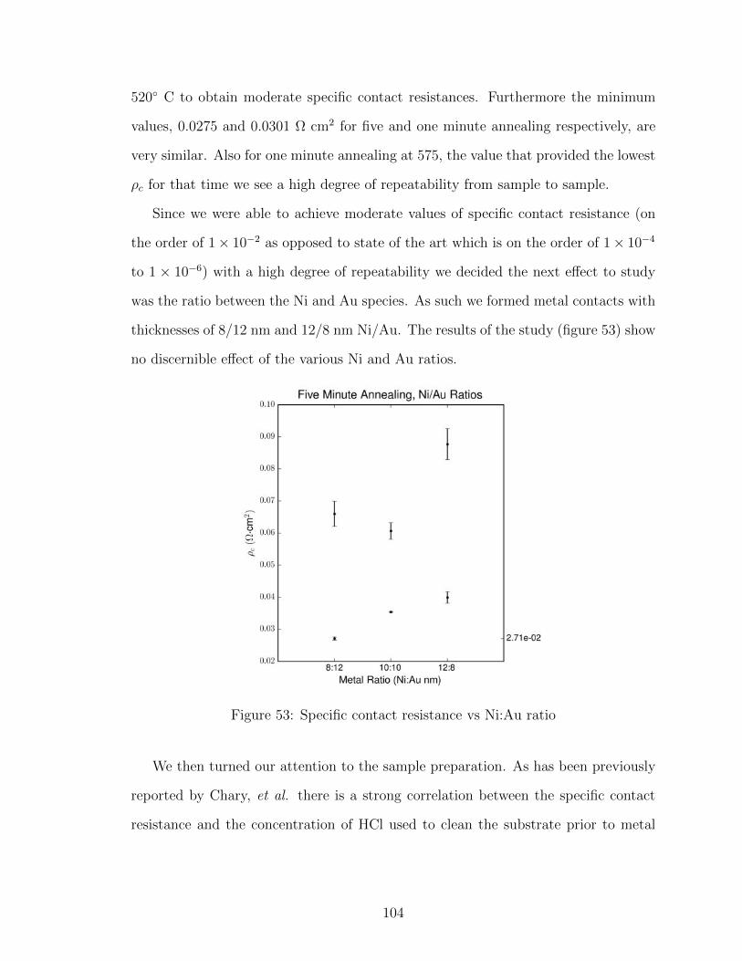
520� C to obtain moderate specific contact resistances. Furthermore the minimum
values, 0.0275 and 0.0301 ⌦ cm2 for five and one minute annealing respectively, are
very similar. Also for one minute annealing at 575, the value that provided the lowest
⇢c for that time we see a high degree of repeatability from sample to sample.
Since we were able to achieve moderate values of specific contact resistance (on
the order of 1⇥ 10�2 as opposed to state of the art which is on the order of 1⇥ 10�4
to 1 ⇥ 10�6) with a high degree of repeatability we decided the next e↵ect to study
was the ratio between the Ni and Au species. As such we formed metal contacts with
thicknesses of 8/12 nm and 12/8 nm Ni/Au. The results of the study (figure 53) show
no discernible e↵ect of the various Ni and Au ratios.
Figure 53: Specific contact resistance vs Ni:Au ratio
We then turned our attention to the sample preparation. As has been previously
reported by Chary, et al. there is a strong correlation between the specific contact
resistance and the concentration of HCl used to clean the substrate prior to metal
104
deposition[155]. We first used standard organic cleaning (acetone followed by iso-
propyl alcohol followed by DI-H2
O) to descum the sample. After organic cleaning
we used a bilayer photolithography process with LOR-3b and SC1813 photoresists to
form the TLM patterns. We attempted to replicate the result of Chary, et al. by
cleaning the sample in a HCl:H2
O ranging in dilution ratios of 1:1, 2:1, 3:1, and 1:0 or
pure concentrated HCl (37.5%)[155]. We found that HCl cleaning after photolithog-
raphy did not degrade the bilayer photoresist and the hope is to impede potential
native oxide growth by limiting the time between the acid cleaning and the beginning
of metal deposition. Chary, et al. reported that they cleaned their samples for 10 mins
in the various solutions at room temperature. We replicated this and also attempted
a 5 minute cleaning process. Following metal deposition the photoresist and excess
metal was removed in a commercially available lifto↵ tool using pressurized DMSO
and annealed for one minute in an oxygen ambient at 575� C. The results in figure 54
Figure 54: Specific contact resistance vs HCl:H2
O ratio
show no e↵ect of the various cleaning solutions. The only e↵ect we found was that
105
for one of the samples cleaned in pure HCl the surface of the contacts after metal
metal deposition and lifto↵ was degraded and ohmic contact could not be achieved.
Otherwise, no correlation between the cleaning solutions and the specific contact re-
sistance can be determined. This may be because some as yet undetermined variable
in the process overshadows the e↵ect of the cleaning and leads to a specific contact
resistance between 0.03 and 0.04 ⌦ cm2. On the other hand the reported e↵ect of
cleaning is high (3⇥10�2 ⌦ cm2 to 3⇥10�4 ⌦ cm2 by just changing the HCl:H2
O
ratio), and we simply do not see that in our results[155].
We have also analyzed the e↵ect of annealing the p-GaN in oxygen prior to metal
contact deposition (⇢c = (8.5 ± 1.1) ⇥ 10�2 ⌦ cm2), and annealing 8/12 nm Ni/Au
films at 600� C (⇢c = (2.45 ± 0.22) ⇥ 10�2 ⌦ cm2), but again the results show very
little change in the specific contact resistance. A summary table of all the metal
p-GaN contact measurements is shown in table 11.
106
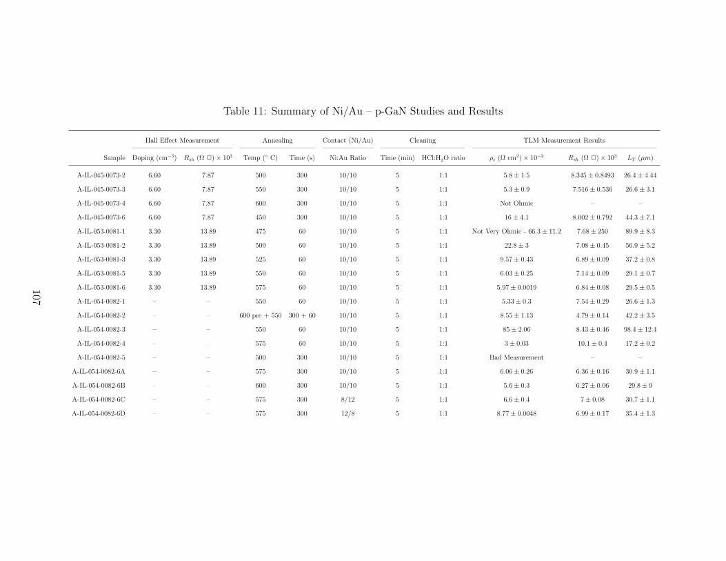
Table 11: Summary of Ni/Au – p-GaN Studies and Results
Hall E↵ect Measurement Annealing Contact (Ni/Au) Cleaning TLM Measurement Results
Sample Doping (cm�3) Rsh (⌦ 2) ⇥ 103 Temp (� C) Time (s) Ni:Au Ratio Time (min) HCl:H2
O ratio ⇢c (⌦ cm2) ⇥ 10�2 Rsh (⌦ 2) ⇥ 103 LT (µm)
A-IL-045-0073-2 6.60 7.87 500 300 10/10 5 1:1 5.8 ± 1.5 8.345 ± 0.8493 26.4 ± 4.44
A-IL-045-0073-3 6.60 7.87 550 300 10/10 5 1:1 5.3 ± 0.9 7.516 ± 0.536 26.6 ± 3.1
A-IL-045-0073-4 6.60 7.87 600 300 10/10 5 1:1 Not Ohmic – –
A-IL-045-0073-6 6.60 7.87 450 300 10/10 5 1:1 16 ± 4.1 8.002 ± 0.792 44.3 ± 7.1
A-IL-053-0081-1 3.30 13.89 475 60 10/10 5 1:1 Not Very Ohmic - 66.3 ± 11.2 7.68 ± 250 89.9 ± 8.3
A-IL-053-0081-2 3.30 13.89 500 60 10/10 5 1:1 22.8 ± 3 7.08 ± 0.45 56.9 ± 5.2
A-IL-053-0081-3 3.30 13.89 525 60 10/10 5 1:1 9.57 ± 0.43 6.89 ± 0.09 37.2 ± 0.8
A-IL-053-0081-5 3.30 13.89 550 60 10/10 5 1:1 6.03 ± 0.25 7.14 ± 0.09 29.1 ± 0.7
A-IL-053-0081-6 3.30 13.89 575 60 10/10 5 1:1 5.97 ± 0.0019 6.84 ± 0.08 29.5 ± 0.5
A-IL-054-0082-1 – – 550 60 10/10 5 1:1 5.33 ± 0.3 7.54 ± 0.29 26.6 ± 1.3
A-IL-054-0082-2 – – 600 pre + 550 300 + 60 10/10 5 1:1 8.55 ± 1.13 4.79 ± 0.14 42.2 ± 3.5
A-IL-054-0082-3 – – 550 60 10/10 5 1:1 85 ± 2.06 8.43 ± 0.46 98.4 ± 12.4
A-IL-054-0082-4 – – 575 60 10/10 5 1:1 3 ± 0.03 10.1 ± 0.4 17.2 ± 0.2
A-IL-054-0082-5 – – 500 300 10/10 5 1:1 Bad Measurement – –
A-IL-054-0082-6A – – 575 300 10/10 5 1:1 6.06 ± 0.26 6.36 ± 0.16 30.9 ± 1.1
A-IL-054-0082-6B – – 600 300 10/10 5 1:1 5.6 ± 0.3 6.27 ± 0.06 29.8 ± 9
A-IL-054-0082-6C – – 575 300 8/12 5 1:1 6.6 ± 0.4 7 ± 0.08 30.7 ± 1.1
A-IL-054-0082-6D – – 575 300 12/8 5 1:1 8.77 ± 0.0048 6.99 ± 0.17 35.4 ± 1.3
107
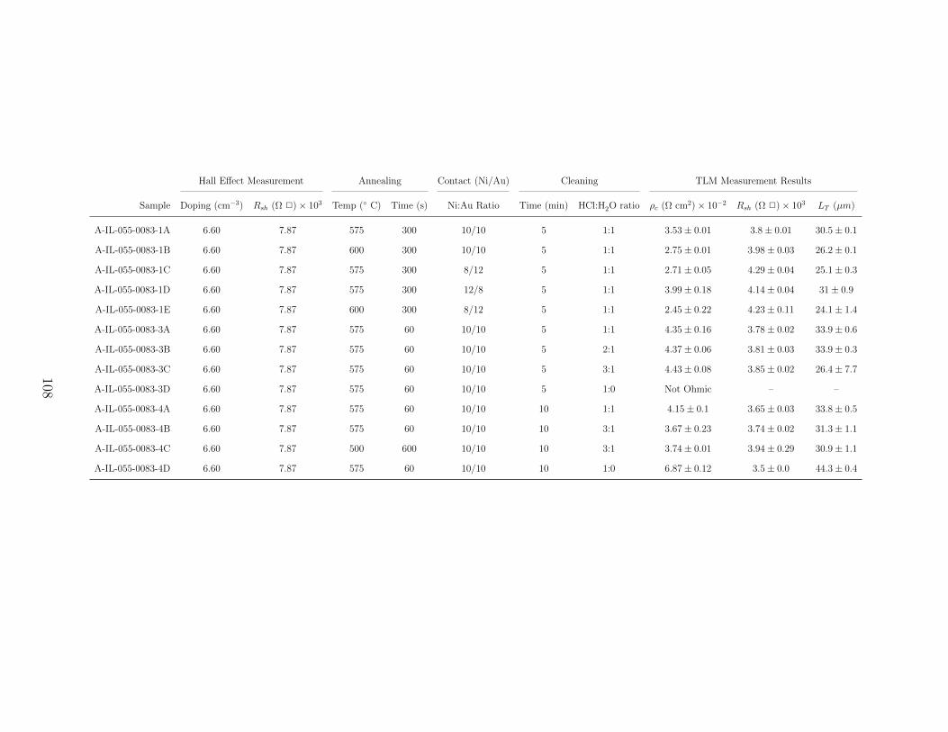
Hall E↵ect Measurement Annealing Contact (Ni/Au) Cleaning TLM Measurement Results
Sample Doping (cm�3) Rsh (⌦ 2) ⇥ 103 Temp (� C) Time (s) Ni:Au Ratio Time (min) HCl:H2
O ratio ⇢c (⌦ cm2) ⇥ 10�2 Rsh (⌦ 2) ⇥ 103 LT (µm)
A-IL-055-0083-1A 6.60 7.87 575 300 10/10 5 1:1 3.53 ± 0.01 3.8 ± 0.01 30.5 ± 0.1
A-IL-055-0083-1B 6.60 7.87 600 300 10/10 5 1:1 2.75 ± 0.01 3.98 ± 0.03 26.2 ± 0.1
A-IL-055-0083-1C 6.60 7.87 575 300 8/12 5 1:1 2.71 ± 0.05 4.29 ± 0.04 25.1 ± 0.3
A-IL-055-0083-1D 6.60 7.87 575 300 12/8 5 1:1 3.99 ± 0.18 4.14 ± 0.04 31 ± 0.9
A-IL-055-0083-1E 6.60 7.87 600 300 8/12 5 1:1 2.45 ± 0.22 4.23 ± 0.11 24.1 ± 1.4
A-IL-055-0083-3A 6.60 7.87 575 60 10/10 5 1:1 4.35 ± 0.16 3.78 ± 0.02 33.9 ± 0.6
A-IL-055-0083-3B 6.60 7.87 575 60 10/10 5 2:1 4.37 ± 0.06 3.81 ± 0.03 33.9 ± 0.3
A-IL-055-0083-3C 6.60 7.87 575 60 10/10 5 3:1 4.43 ± 0.08 3.85 ± 0.02 26.4 ± 7.7
A-IL-055-0083-3D 6.60 7.87 575 60 10/10 5 1:0 Not Ohmic – –
A-IL-055-0083-4A 6.60 7.87 575 60 10/10 10 1:1 4.15 ± 0.1 3.65 ± 0.03 33.8 ± 0.5
A-IL-055-0083-4B 6.60 7.87 575 60 10/10 10 3:1 3.67 ± 0.23 3.74 ± 0.02 31.3 ± 1.1
A-IL-055-0083-4C 6.60 7.87 500 600 10/10 10 3:1 3.74 ± 0.01 3.94 ± 0.29 30.9 ± 1.1
A-IL-055-0083-4D 6.60 7.87 575 60 10/10 10 1:0 6.87 ± 0.12 3.5 ± 0.0 44.3 ± 0.4
108
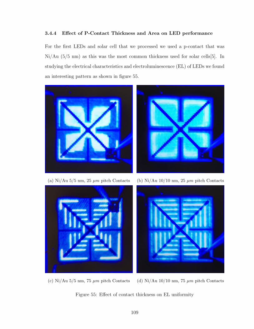
3.4.4 E↵ect of P-Contact Thickness and Area on LED performance
For the first LEDs and solar cell that we processed we used a p-contact that was
Ni/Au (5/5 nm) as this was the most common thickness used for solar cells[5]. In
studying the electrical characteristics and electroluminescence (EL) of LEDs we found
an interesting pattern as shown in figure 55.
(a) Ni/Au 5/5 nm, 25 µm pitch Contacts (b) Ni/Au 10/10 nm, 25 µm pitch Contacts
(c) Ni/Au 5/5 nm, 75 µm pitch Contacts (d) Ni/Au 10/10 nm, 75 µm pitch Contacts
Figure 55: E↵ect of contact thickness on EL uniformity
109
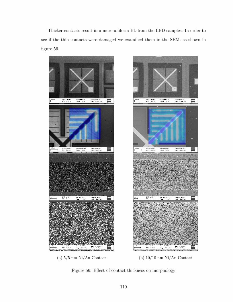
Thicker contacts result in a more uniform EL from the LED samples. In order to
see if the thin contacts were damaged we examined them in the SEM. as shown in
figure 56.
(a) 5/5 nm Ni/Au Contact (b) 10/10 nm Ni/Au Contact
Figure 56: E↵ect of contact thickness on morphology
110
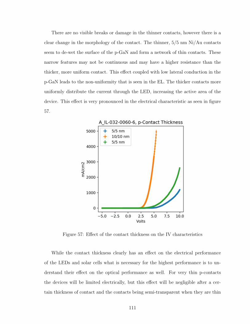
There are no visible breaks or damage in the thinner contacts, however there is a
clear change in the morphology of the contact. The thinner, 5/5 nm Ni/Au contacts
seem to de-wet the surface of the p-GaN and form a network of thin contacts. These
narrow features may not be continuous and may have a higher resistance than the
thicker, more uniform contact. This e↵ect coupled with low lateral conduction in the
p-GaN leads to the non-uniformity that is seen in the EL. The thicker contacts more
uniformly distribute the current through the LED, increasing the active area of the
device. This e↵ect is very pronounced in the electrical characteristic as seen in figure
57.
Figure 57: E↵ect of the contact thickness on the IV characteristics
While the contact thickness clearly has an e↵ect on the electrical performance
of the LEDs and solar cells what is necessary for the highest performance is to un-
derstand their e↵ect on the optical performance as well. For very thin p-contacts
the devices will be limited electrically, but this e↵ect will be negligible after a cer-
tain thickness of contact and the contacts being semi-transparent when they are thin
111
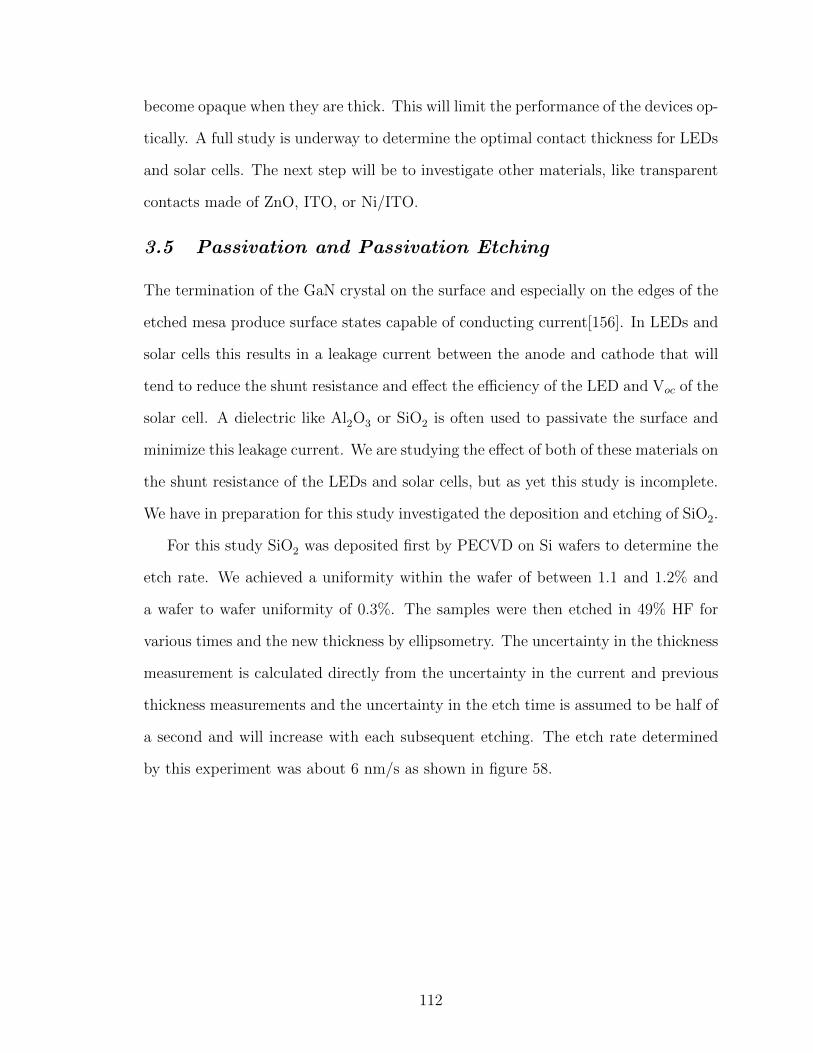
become opaque when they are thick. This will limit the performance of the devices op-
tically. A full study is underway to determine the optimal contact thickness for LEDs
and solar cells. The next step will be to investigate other materials, like transparent
contacts made of ZnO, ITO, or Ni/ITO.
3.5 Passivation and Passivation Etching
The termination of the GaN crystal on the surface and especially on the edges of the
etched mesa produce surface states capable of conducting current[156]. In LEDs and
solar cells this results in a leakage current between the anode and cathode that will
tend to reduce the shunt resistance and e↵ect the e�ciency of the LED and Voc of the
solar cell. A dielectric like Al2
O3
or SiO2
is often used to passivate the surface and
minimize this leakage current. We are studying the e↵ect of both of these materials on
the shunt resistance of the LEDs and solar cells, but as yet this study is incomplete.
We have in preparation for this study investigated the deposition and etching of SiO2
.
For this study SiO2
was deposited first by PECVD on Si wafers to determine the
etch rate. We achieved a uniformity within the wafer of between 1.1 and 1.2% and
a wafer to wafer uniformity of 0.3%. The samples were then etched in 49% HF for
various times and the new thickness by ellipsometry. The uncertainty in the thickness
measurement is calculated directly from the uncertainty in the current and previous
thickness measurements and the uncertainty in the etch time is assumed to be half of
a second and will increase with each subsequent etching. The etch rate determined
by this experiment was about 6 nm/s as shown in figure 58.
112
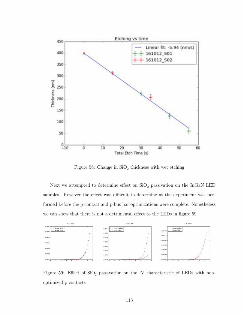
Figure 58: Change in SiO2
thickness with wet etching
Next we attempted to determine e↵ect on SiO2
passivation on the InGaN LED
samples. However the e↵ect was di�cult to determine as the experiment was per-
formed before the p-contact and p-bus bar optimizations were complete. Nonetheless
we can show that there is not a detrimental e↵ect to the LEDs in figure 59.
Figure 59: E↵ect of SiO2
passivation on the IV characteristic of LEDs with non-
optimized p-contacts
113
3.6 Conclusions and Next Steps
We have deconstructed each step of the process in making InGaN based LEDs and
solar cells. We have achieved very uniform and repeatable results for nitride etching.
We have also studied the e↵ect of v-pits on InGaN based solar cells and demonstrated
that we can fill the v-pits using a cured HSQ resin. We still have to show the v-pit
passivation will enhance the Voc of solar cells with low-temperature p-GaN. On the
n-contacts we concluded that a Ti/Al/Ni/Au structure was both more stable and
resulted in a better morphology after annealing both a two-step Ti/Al n-contact
with a Ni/Al/Ni/Au bus bar and a one-step contact of Ti/Al/Ni/Al/Ni/Au contact.
We have also made significant progress in optimizing Ni/Au contacting to p-GaN,
however this remains a challenge.
We see a decrease in the specific contact resistance of Ni/Au p-contacts with the
annealing temperature until about 625� C. There is no clear trend from the studies of
HCl cleaning and small variations in Ni:Au ratio. For now we can repeatably achieve
ohmic p-type contacts with a moderate specific contact resistance of 2–4⇥10�2 ⌦
cm2. It is not clear how to proceed to achieve p-contacts with a lower specific contact
resistance. The literature suggests a few mechanisms that appear to be correlated with
ohmic contact formation on p-GaN but the strength and even validity of each of these
mechanisms is still under debate. Assuming that Ni/Au contacts annealed in oxygen
have a layer of NiO on the surface there may be some resistance added to the structure
that is measured as specific contact resistance but in reality is based on the material.
Furthermore the thin quality of the contacts may make the simplification that the
contact resistance is greater than the material resistance of the metal contacts false.
Therefore simply increasing the amount of Au will improve the measured specific
contact resistance. This is because the surface and amount of Ni remain constant
while the overall thickness of the contact increases. This increase of thickness will
lower the resistance of the metal in itself and the amount of NiO on the surface will
114
decrease also as more Ni will remain in the solid solution instead of out-di↵use at
the surface in contact with oxide (assuming the process is di↵usion limited). Also
there are mixed results as to the e↵ect of HCl cleaning of the sample. Perhaps a
di↵erent solution (HF, aqua regia (HNO3
:HCl 1:3), boiling KOH are all mentioned in
the literature) will have better results.
Optimizing p-contact thickness is critical for device performance. Thicker p-
contacts result in better current spreading, but at a potential loss of optical trans-
parency. The performance vs Ni/Au p-contact thickness of the LEDs and solar cells
should be studied as well as the transparency vs thickness using FTIR. These results
should be compared against results obtained using a transparent contact like ITO.
We have taken the first steps towards optimizing the mesa passivation required
to achieve a high shunt resistance. We have shown that the deposition and etching
of SiO2
is very uniform but have yet to perform an in-depth study on the e↵ect of
di↵erent dielectric deposition recipes and materials on the shunt resistance. Finally,
a study of antireflective coatings should be done to decrease the loss due to optical
reflections. These may be deposited in addition to or in parallel with the passivation
materials.
In conclusion we have taken the first steps towards a fully optimized process for
of high-e�ciency LEDs and solar cells. This has resulted in encouraging results for
both large (1 cm2) and small size solar cells and LEDs. Furthermore, we have laid
out a clear experimental pathway to move forward and increase the performance of
these devices.
115
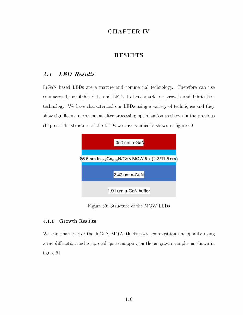
CHAPTER IV
RESULTS
4.1 LED Results
InGaN based LEDs are a mature and commercial technology. Therefore can use
commercially available data and LEDs to benchmark our growth and fabrication
technology. We have characterized our LEDs using a variety of techniques and they
show significant improvement after processing optimization as shown in the previous
chapter. The structure of the LEDs we have studied is shown in figure 60
Figure 60: Structure of the MQW LEDs
4.1.1 Growth Results
We can characterize the InGaN MQW thicknesses, composition and quality using
x-ray di↵raction and reciprocal space mapping on the as-grown samples as shown in
figure 61.
116
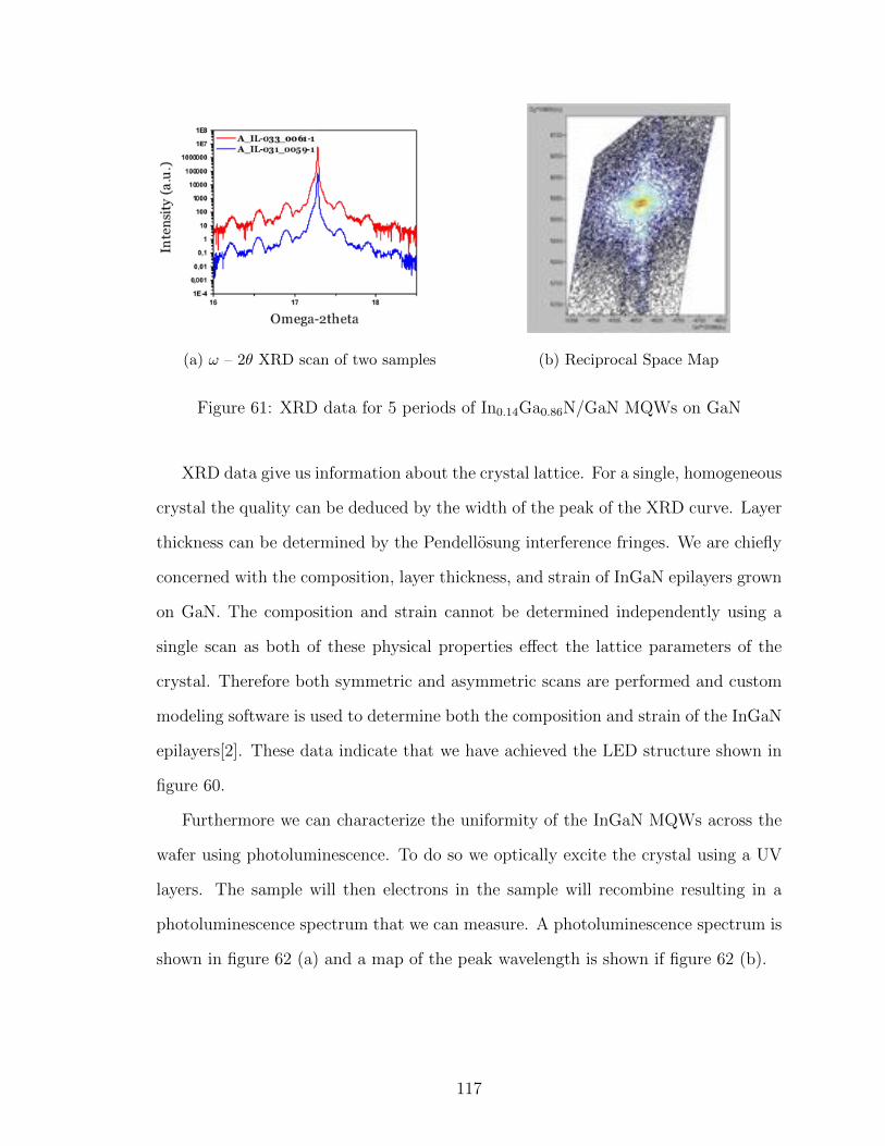
(a) ! – 2✓ XRD scan of two samples (b) Reciprocal Space Map
Figure 61: XRD data for 5 periods of In0.14
Ga0.86
N/GaN MQWs on GaN
XRD data give us information about the crystal lattice. For a single, homogeneous
crystal the quality can be deduced by the width of the peak of the XRD curve. Layer
thickness can be determined by the Pendellosung interference fringes. We are chiefly
concerned with the composition, layer thickness, and strain of InGaN epilayers grown
on GaN. The composition and strain cannot be determined independently using a
single scan as both of these physical properties e↵ect the lattice parameters of the
crystal. Therefore both symmetric and asymmetric scans are performed and custom
modeling software is used to determine both the composition and strain of the InGaN
epilayers[2]. These data indicate that we have achieved the LED structure shown in
figure 60.
Furthermore we can characterize the uniformity of the InGaN MQWs across the
wafer using photoluminescence. To do so we optically excite the crystal using a UV
layers. The sample will then electrons in the sample will recombine resulting in a
photoluminescence spectrum that we can measure. A photoluminescence spectrum is
shown in figure 62 (a) and a map of the peak wavelength is shown if figure 62 (b).
117
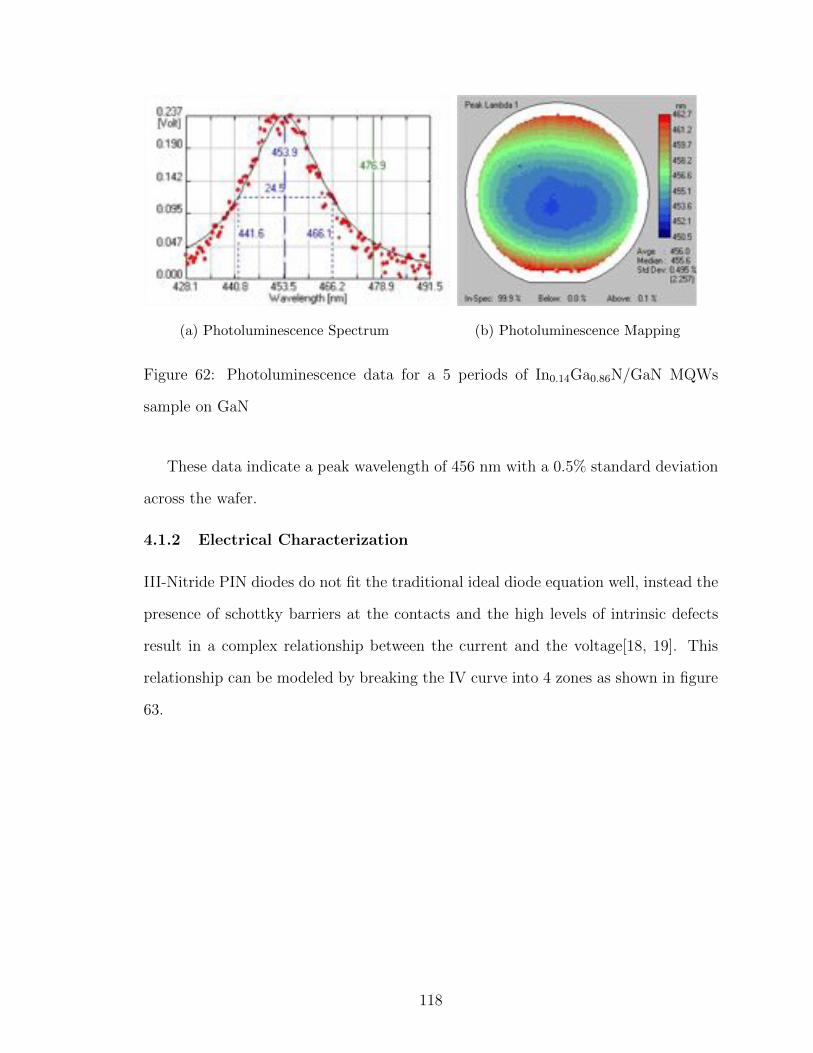
(a) Photoluminescence Spectrum (b) Photoluminescence Mapping
Figure 62: Photoluminescence data for a 5 periods of In0.14
Ga0.86
N/GaN MQWs
sample on GaN
These data indicate a peak wavelength of 456 nm with a 0.5% standard deviation
across the wafer.
4.1.2 Electrical Characterization
III-Nitride PIN diodes do not fit the traditional ideal diode equation well, instead the
presence of schottky barriers at the contacts and the high levels of intrinsic defects
result in a complex relationship between the current and the voltage[18, 19]. This
relationship can be modeled by breaking the IV curve into 4 zones as shown in figure
63.
118
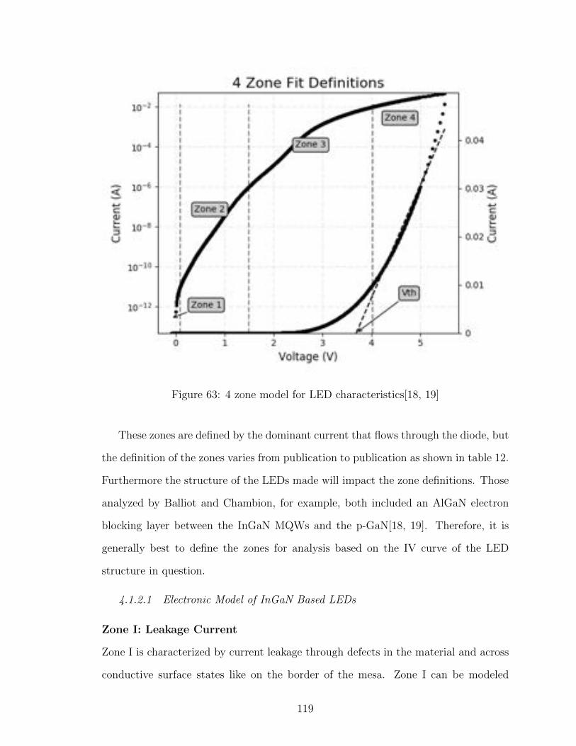
Figure 63: 4 zone model for LED characteristics[18, 19]
These zones are defined by the dominant current that flows through the diode, but
the definition of the zones varies from publication to publication as shown in table 12.
Furthermore the structure of the LEDs made will impact the zone definitions. Those
analyzed by Balliot and Chambion, for example, both included an AlGaN electron
blocking layer between the InGaN MQWs and the p-GaN[18, 19]. Therefore, it is
generally best to define the zones for analysis based on the IV curve of the LED
structure in question.
4.1.2.1 Electronic Model of InGaN Based LEDs
Zone I: Leakage Current
Zone I is characterized by current leakage through defects in the material and across
conductive surface states like on the border of the mesa. Zone I can be modeled
119
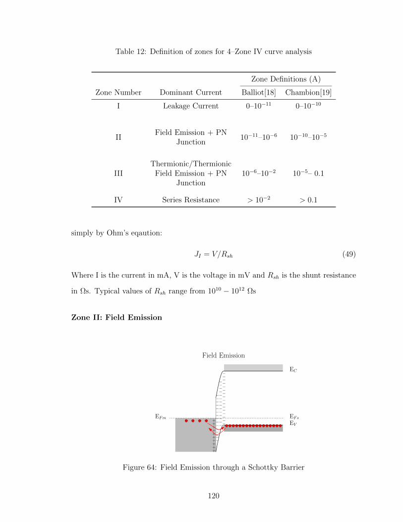
Table 12: Definition of zones for 4–Zone IV curve analysis
Zone Definitions (A)
Zone Number Dominant Current Balliot[18] Chambion[19]
I Leakage Current 0–10�11 0–10�10
IIField Emission + PN
Junction10�11–10�6 10�10–10�5
IIIThermionic/ThermionicField Emission + PN
Junction10�6–10�2 10�5– 0.1
IV Series Resistance > 10�2 > 0.1
simply by Ohm’s eqaution:
JI = V/Rsh (49)
Where I is the current in mA, V is the voltage in mV and Rsh is the shunt resistance
in ⌦s. Typical values of Rsh range from 1010 � 1012 ⌦s
Zone II: Field Emission
EFm
EC
EV
EFs
++++++++++
���������������
��������������
��
�����������
��
Field Emission
�
�
Figure 64: Field Emission through a Schottky Barrier
120
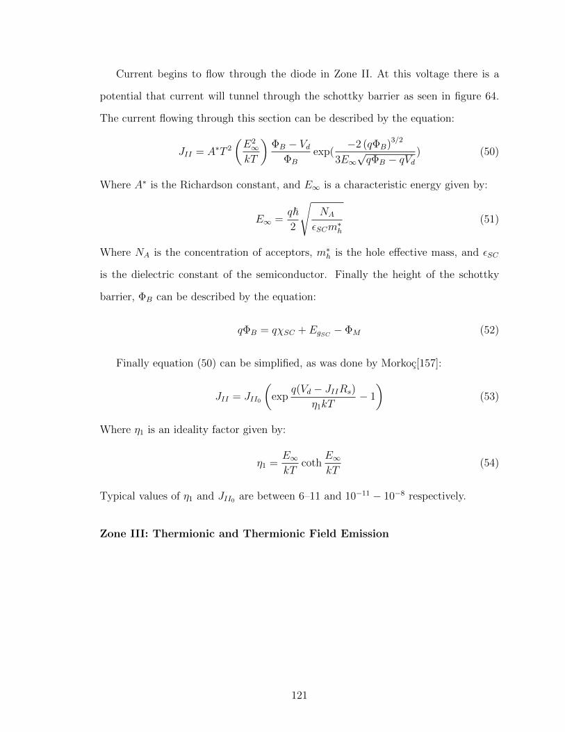
Current begins to flow through the diode in Zone II. At this voltage there is a
potential that current will tunnel through the schottky barrier as seen in figure 64.
The current flowing through this section can be described by the equation:
JII = A⇤T 2
✓E2
1kT
◆�B � Vd
�B
exp(�2 (q�B)3/2
3E1pq�B � qVd
) (50)
Where A⇤ is the Richardson constant, and E1 is a characteristic energy given by:
E1 =q~2
sNA
✏SCm⇤h
(51)
Where NA is the concentration of acceptors, m⇤h is the hole e↵ective mass, and ✏SC
is the dielectric constant of the semiconductor. Finally the height of the schottky
barrier, �B can be described by the equation:
q�B = q�SC + EgSC
� �M (52)
Finally equation (50) can be simplified, as was done by Morkoc[157]:
JII = JII0
✓exp
q(Vd � JIIRs)
⌘1
kT� 1
◆(53)
Where ⌘1
is an ideality factor given by:
⌘1
=E1
kTcoth
E1
kT(54)
Typical values of ⌘1
and JII0
are between 6–11 and 10�11 � 10�8 respectively.
Zone III: Thermionic and Thermionic Field Emission
121
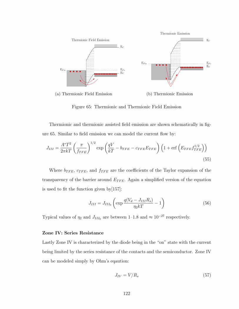
EFm
EC
EV
EFs
++++++++++
���������������
��������������
�������������
��������������
�������������
Thermionic Field Emission
��
��
��
(a) Thermionic Field Emission
EFm
EC
EV
EFs
++++++++++
����������������
���������������
���������������
���������������
��������������
���������������
Thermionic Emission
(b) Thermionic Emission
Figure 65: Thermionic and Thermionic Field Emission
Thermionic and thermionic assisted field emission are shown schematically in fig-
ure 65. Similar to field emission we can model the current flow by:
JIII =A⇤T 2
2⇡kT
✓⇡
fTFE
◆1/2
exp
✓qV
kT� bTFE � cTFEETFE
◆⇣1 + erf
⇣ETFEf
1/2TFE
⌘⌘
(55)
Where bTFE, cTFE, and fTFE are the coe�cients of the Taylor expansion of the
transparency of the barrier around ETFE. Again a simplified version of the equation
is used to fit the function given by[157]:
JIII = JIII0
✓exp
q(Vd � JIIIRs)
⌘2
kT� 1
◆(56)
Typical values of ⌘2
and JIII0
are between 1–1.8 and ⇡ 10�27 respectively.
Zone IV: Series Resistance
Lastly Zone IV is characterized by the diode being in the “on” state with the current
being limited by the series resistance of the contacts and the semiconductor. Zone IV
can be modeled simply by Ohm’s eqaution:
JIV = V/Rs (57)
122
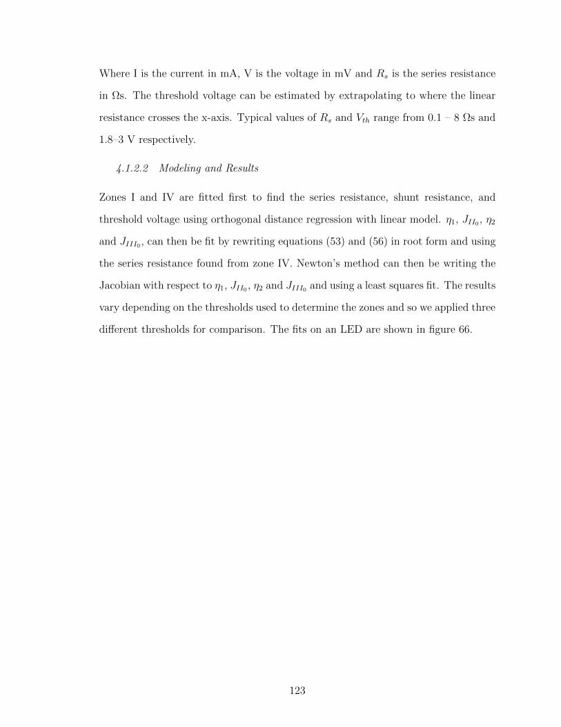
Where I is the current in mA, V is the voltage in mV and Rs is the series resistance
in ⌦s. The threshold voltage can be estimated by extrapolating to where the linear
resistance crosses the x-axis. Typical values of Rs and Vth range from 0.1 – 8 ⌦s and
1.8–3 V respectively.
4.1.2.2 Modeling and Results
Zones I and IV are fitted first to find the series resistance, shunt resistance, and
threshold voltage using orthogonal distance regression with linear model. ⌘1
, JII0
, ⌘2
and JIII0
, can then be fit by rewriting equations (53) and (56) in root form and using
the series resistance found from zone IV. Newton’s method can then be writing the
Jacobian with respect to ⌘1
, JII0
, ⌘2
and JIII0
and using a least squares fit. The results
vary depending on the thresholds used to determine the zones and so we applied three
di↵erent thresholds for comparison. The fits on an LED are shown in figure 66.
123
(a) Balliot Threshold[18] (b) Chambion Threshold[19]
(c) Deterministic Threshold
Figure 66: Four Zone fits to an LED
As can be seen from figure 66, the fits are pretty good which is surprising given
that our LEDs are lacking an electron blocking layer. Furthermore it is evident that
the fits to zones 1, 2, and 4 are quite close to typical values found in commercial
LEDs. The shunt resistance is lower than desired, but this is likely due to the lack
of optimized passivation on this sample. In addition the series resistance remains
an order of magnitude too large, but this can be lowered by further optimizing the
contacts. Zone III is not fit well and also the fitted values are far from the ideal
suggesting that further work is necessary optimizing the contacts and the material
structure.
124

Table 13: Comparison of IV curve figures of merit using di↵erent zone thresholds
Thresholds
Figure of Merit Balliot[18] Chambion[19] Deterministic Typical Value
Rsh 9 ⇥ 109 4 ⇥ 109 4 ⇥ 109 1010 � 1012
JII0
9 ⇥ 10�11 6 ⇥ 10�10 1.5 ⇥ 10�10 10�11 � 10�8
⌘1
6 8 7 6 � 11
JIII0
2 ⇥ 10�7 2 ⇥ 10�7 2 ⇥ 10�7 ⇡ 10�27
⌘2
13 13 13 1 � 1.8
Rs 43 43 42 0.1 � 8
Vth 3.69 3.69 3.69 1.8 � 3
4.1.3 Optical Results
Figure 67: Electroluminescence Measurements
The LEDs Illuminate well with a peak at 459 nm and a FWHM of 24 nm. This is as
expected from the PL measurement. Furthermore the optical power vs the current
remains linear up above 70 mA.
125
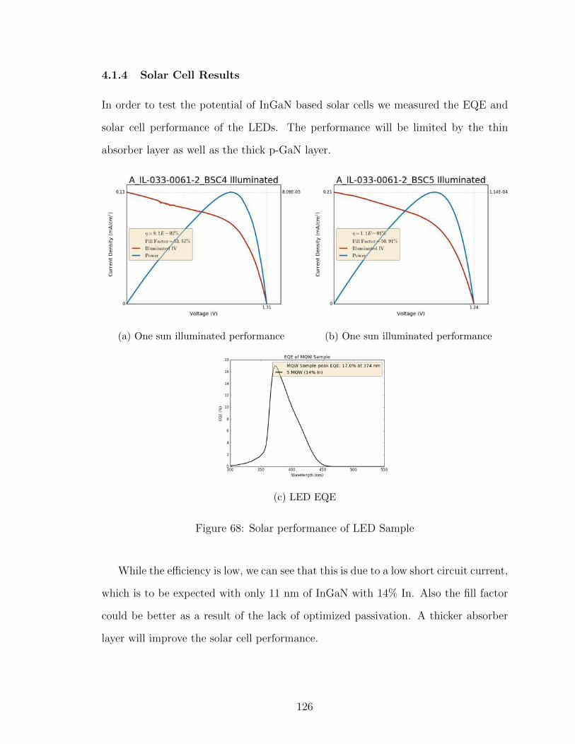
4.1.4 Solar Cell Results
In order to test the potential of InGaN based solar cells we measured the EQE and
solar cell performance of the LEDs. The performance will be limited by the thin
absorber layer as well as the thick p-GaN layer.
(a) One sun illuminated performance (b) One sun illuminated performance
(c) LED EQE
Figure 68: Solar performance of LED Sample
While the e�ciency is low, we can see that this is due to a low short circuit current,
which is to be expected with only 11 nm of InGaN with 14% In. Also the fill factor
could be better as a result of the lack of optimized passivation. A thicker absorber
layer will improve the solar cell performance.
126
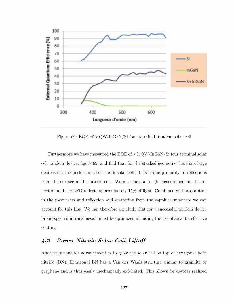
Figure 69: EQE of MQW-InGaN/Si four terminal, tandem solar cell
Furthermore we have measured the EQE of a MQW-InGaN/Si four terminal solar
cell tandem device, figure 69, and find that for the stacked geometry there is a large
decrease in the performance of the Si solar cell. This is due primarily to reflections
from the surface of the nitride cell. We also have a rough measurement of the re-
flection and the LED reflects approximately 15% of light. Combined with absorption
in the p-contacts and reflection and scattering from the sapphire substrate we can
account for this loss. We can therefore conclude that for a successful tandem device
broad-spectrum transmission must be optimized including the use of an anti-reflective
coating.
4.2 Boron Nitride Solar Cell Lifto↵
Another avenue for advancement is to grow the solar cell on top of hexagonal born
nitride (BN). Hexagonal BN has a Van der Waals structure similar to graphite or
graphene and is thus easily mechanically exfoliated. This allows for devices realized
127

on top of BN to be easily separated from the substrate on which they were grown[158].
This has application for solar cells because the devices could be removed from the
sapphire substrate and placed either on a smaller band gap solar cell like Si to form
a tandem, or on a heat sink increasing the e�ciency of concentrated photovoltaics.
Furthermore for solar cells it allows for backside processing of n-contacts that can also
serve as rear reflectors. The same qualities that allow for easy lift o↵ also make device
fabrication a challenge. Extra care must be taken when processing the materials in
solution and performing standard fabrication techniques like metal lift o↵ to not also
remove the active film. We have some expertise in this area and have realized UV
photodetectors using a thin hexagonal BN film. The BN photodetectors are shown
in figure 70.
128
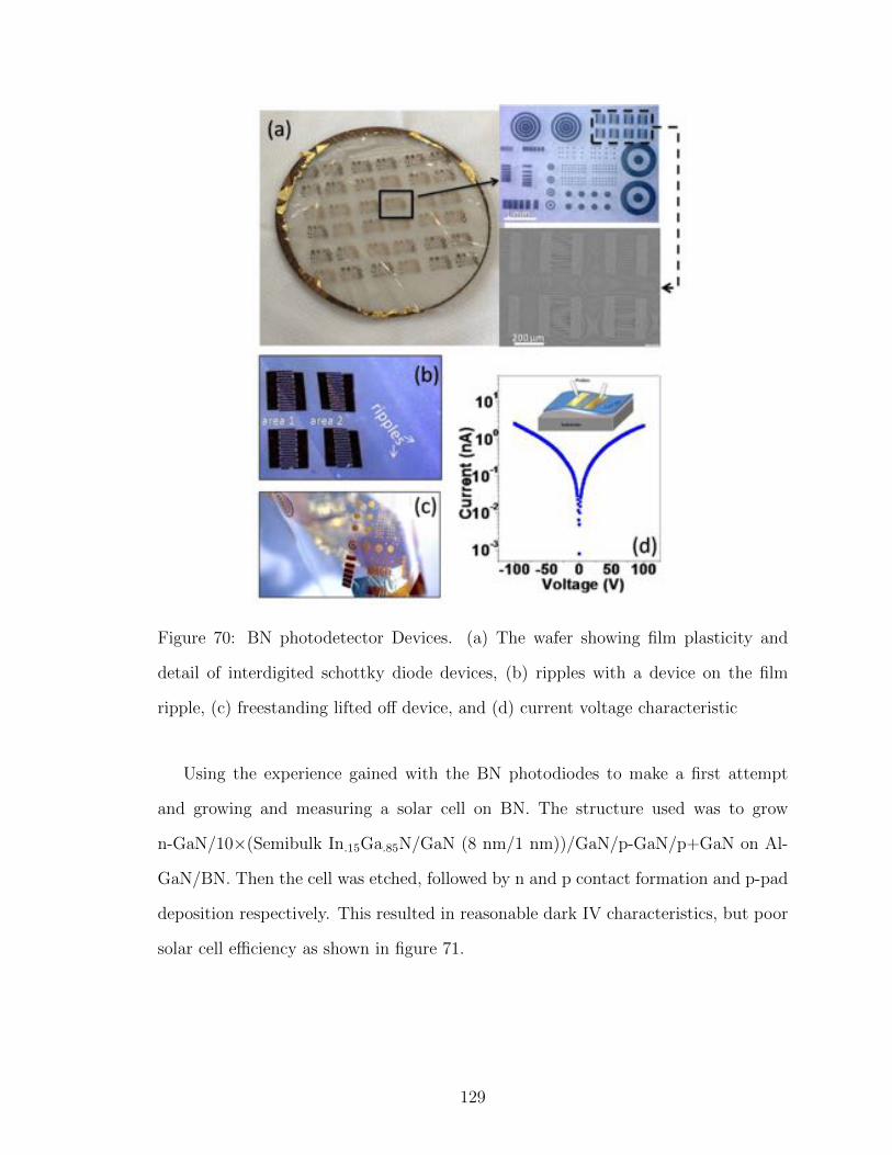
Figure 70: BN photodetector Devices. (a) The wafer showing film plasticity and
detail of interdigited schottky diode devices, (b) ripples with a device on the film
ripple, (c) freestanding lifted o↵ device, and (d) current voltage characteristic
Using the experience gained with the BN photodiodes to make a first attempt
and growing and measuring a solar cell on BN. The structure used was to grow
n-GaN/10⇥(Semibulk In.15
Ga.85
N/GaN (8 nm/1 nm))/GaN/p-GaN/p+GaN on Al-
GaN/BN. Then the cell was etched, followed by n and p contact formation and p-pad
deposition respectively. This resulted in reasonable dark IV characteristics, but poor
solar cell e�ciency as shown in figure 71.
129
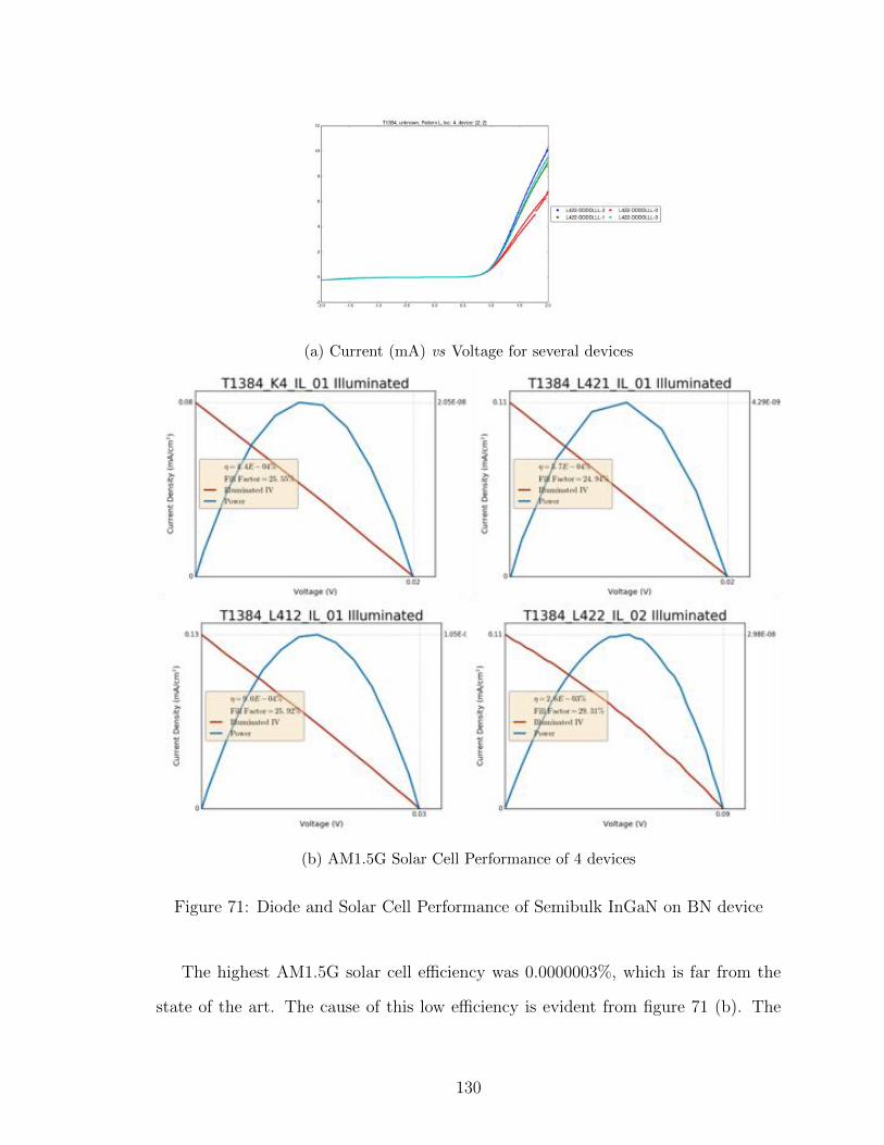
(a) Current (mA) vs Voltage for several devices
(b) AM1.5G Solar Cell Performance of 4 devices
Figure 71: Diode and Solar Cell Performance of Semibulk InGaN on BN device
The highest AM1.5G solar cell e�ciency was 0.0000003%, which is far from the
state of the art. The cause of this low e�ciency is evident from figure 71 (b). The
130
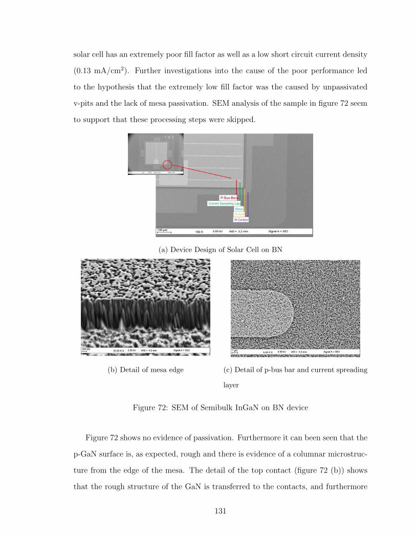
solar cell has an extremely poor fill factor as well as a low short circuit current density
(0.13 mA/cm2). Further investigations into the cause of the poor performance led
to the hypothesis that the extremely low fill factor was the caused by unpassivated
v-pits and the lack of mesa passivation. SEM analysis of the sample in figure 72 seem
to support that these processing steps were skipped.
(a) Device Design of Solar Cell on BN
(b) Detail of mesa edge (c) Detail of p-bus bar and current spreading
layer
Figure 72: SEM of Semibulk InGaN on BN device
Figure 72 shows no evidence of passivation. Furthermore it can been seen that the
p-GaN surface is, as expected, rough and there is evidence of a columnar microstruc-
ture from the edge of the mesa. The detail of the top contact (figure 72 (b)) shows
that the rough structure of the GaN is transferred to the contacts, and furthermore
131
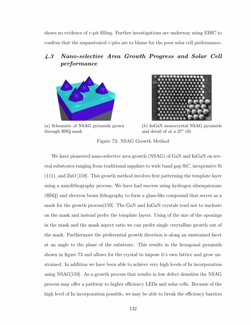
shows no evidence of v-pit filling. Further investigations are underway using EBIC to
confirm that the unpassivated v-pits are to blame for the poor solar cell performance.
4.3 Nano-selective Area Growth Progress and Solar Cell
performance
(a) Schematic of NSAG pyramids grownthrough HSQ mask
(b) InGaN monocrystal NSAG pyramidsand detail of at a 37� tilt
Figure 73: NSAG Growth Method
We have pioneered nano-selective area growth (NSAG) of GaN and InGaN on sev-
eral substrates ranging from traditional sapphire to wide band gap SiC, inexpensive Si
(111), and ZnO [159]. This growth method involves first patterning the template layer
using a nanolithography process. We have had success using hydrogen silsesquioxane
(HSQ) and electron beam lithography to form a glass-like compound that serves as a
mask for the growth process[159]. The GaN and InGaN crystals tend not to nucleate
on the mask and instead prefer the template layers. Using of the size of the openings
in the mask and the mask aspect ratio we can prefer single crsytalline growth out of
the mask. Furthermore the preferential growth direction is along an unstrained facet
at an angle to the plane of the substrate. This results in the hexagonal pyramids
shown in figure 73 and allows for the crystal to impose it’s own lattice and grow un-
strained. In addition we have been able to achieve very high levels of In incorporation
using NSAG[159]. As a growth process that results in low defect densities the NSAG
process may o↵er a pathway to higher e�ciency LEDs and solar cells. Because of the
high level of In incorporation possible, we may be able to break the e�ciency barriers
132
limiting InGaN solar cells (that are mostly limited because they are transparent to
the majority of the solar spectrum) or potentially make green and white light LEDs.
4.3.1 NSAG Process Development with the CEA
We briefly collaborated with the commissariat a l’energie atomique or CEA on a
process involving NSAG for LEDs. The idea was to show that NSAG could be used
to make LEDs and simplify the fabrication process by eliminating GaN ICP etching.
The project called for large area nanolithography which is a challenge because of the
time required to write large patterns using electron beam lithography. Furthermore
the sensitivity of HSQ electron beam resist can vary with time before exposure, and
so careful optimization of the first step was required. The proposed process is shown
in figure 74. As can be seen it is a simple process that requires only wet etching
and contact formation. The primary challenges are the formation of the SiO2
during
nanolithography and achieving epitaxial lateral over growth (ELOG) of the p-GaN.
133
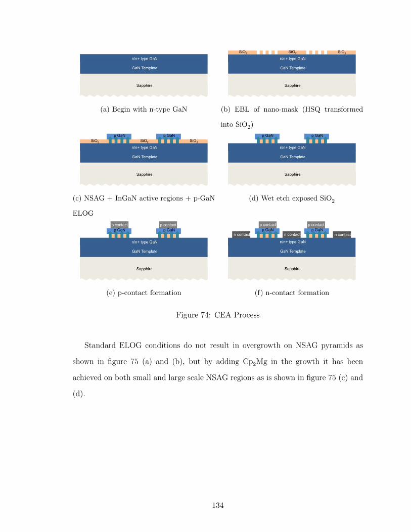
(a) Begin with n-type GaN (b) EBL of nano-mask (HSQ transformed
into SiO2
)
(c) NSAG + InGaN active regions + p-GaN
ELOG
(d) Wet etch exposed SiO2
(e) p-contact formation (f) n-contact formation
Figure 74: CEA Process
Standard ELOG conditions do not result in overgrowth on NSAG pyramids as
shown in figure 75 (a) and (b), but by adding Cp2
Mg in the growth it has been
achieved on both small and large scale NSAG regions as is shown in figure 75 (c) and
(d).
134
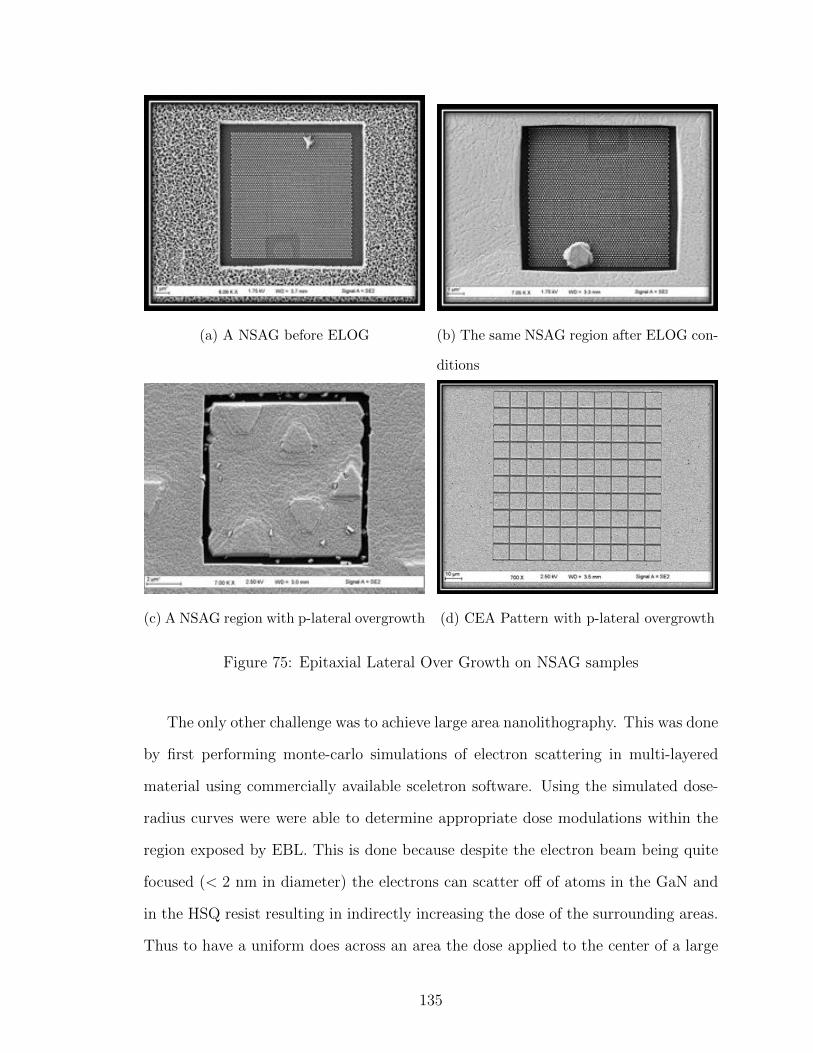
(a) A NSAG before ELOG (b) The same NSAG region after ELOG con-
ditions
(c) A NSAG region with p-lateral overgrowth (d) CEA Pattern with p-lateral overgrowth
Figure 75: Epitaxial Lateral Over Growth on NSAG samples
The only other challenge was to achieve large area nanolithography. This was done
by first performing monte-carlo simulations of electron scattering in multi-layered
material using commercially available sceletron software. Using the simulated dose-
radius curves were were able to determine appropriate dose modulations within the
region exposed by EBL. This is done because despite the electron beam being quite
focused (< 2 nm in diameter) the electrons can scatter o↵ of atoms in the GaN and
in the HSQ resist resulting in indirectly increasing the dose of the surrounding areas.
Thus to have a uniform does across an area the dose applied to the center of a large
135

pattern should be less than the dose on the edges. The dose correction is pattern
dependent, and we show the nanolithography pattern as well as the dose correction
in figure 76.
136
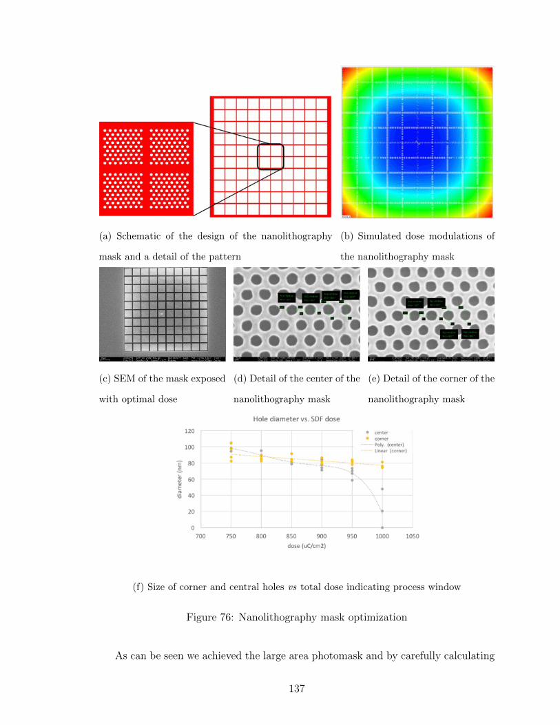
(a) Schematic of the design of the nanolithography
mask and a detail of the pattern
(b) Simulated dose modulations of
the nanolithography mask
(c) SEM of the mask exposed
with optimal dose
(d) Detail of the center of the
nanolithography mask
(e) Detail of the corner of the
nanolithography mask
(f) Size of corner and central holes vs total dose indicating process window
Figure 76: Nanolithography mask optimization
As can be seen we achieved the large area photomask and by carefully calculating
137
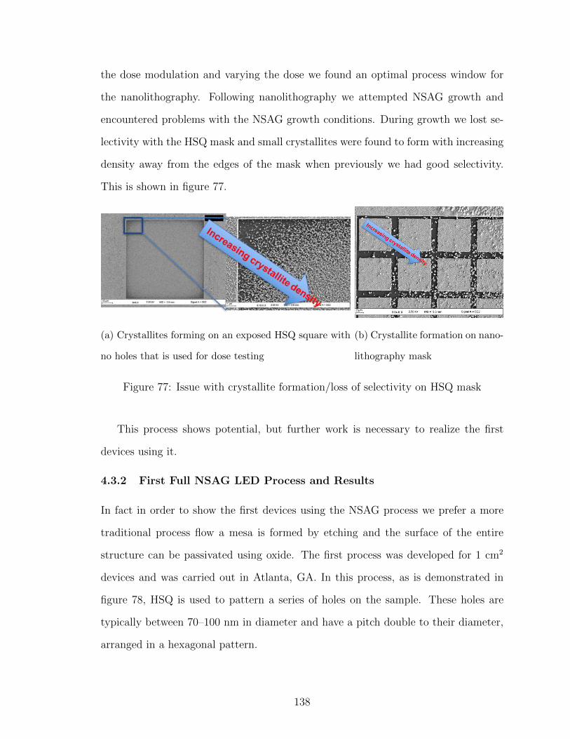
the dose modulation and varying the dose we found an optimal process window for
the nanolithography. Following nanolithography we attempted NSAG growth and
encountered problems with the NSAG growth conditions. During growth we lost se-
lectivity with the HSQ mask and small crystallites were found to form with increasing
density away from the edges of the mask when previously we had good selectivity.
This is shown in figure 77.
(a) Crystallites forming on an exposed HSQ square with
no holes that is used for dose testing
(b) Crystallite formation on nano-
lithography mask
Figure 77: Issue with crystallite formation/loss of selectivity on HSQ mask
This process shows potential, but further work is necessary to realize the first
devices using it.
4.3.2 First Full NSAG LED Process and Results
In fact in order to show the first devices using the NSAG process we prefer a more
traditional process flow a mesa is formed by etching and the surface of the entire
structure can be passivated using oxide. The first process was developed for 1 cm2
devices and was carried out in Atlanta, GA. In this process, as is demonstrated in
figure 78, HSQ is used to pattern a series of holes on the sample. These holes are
typically between 70–100 nm in diameter and have a pitch double to their diameter,
arranged in a hexagonal pattern.
138
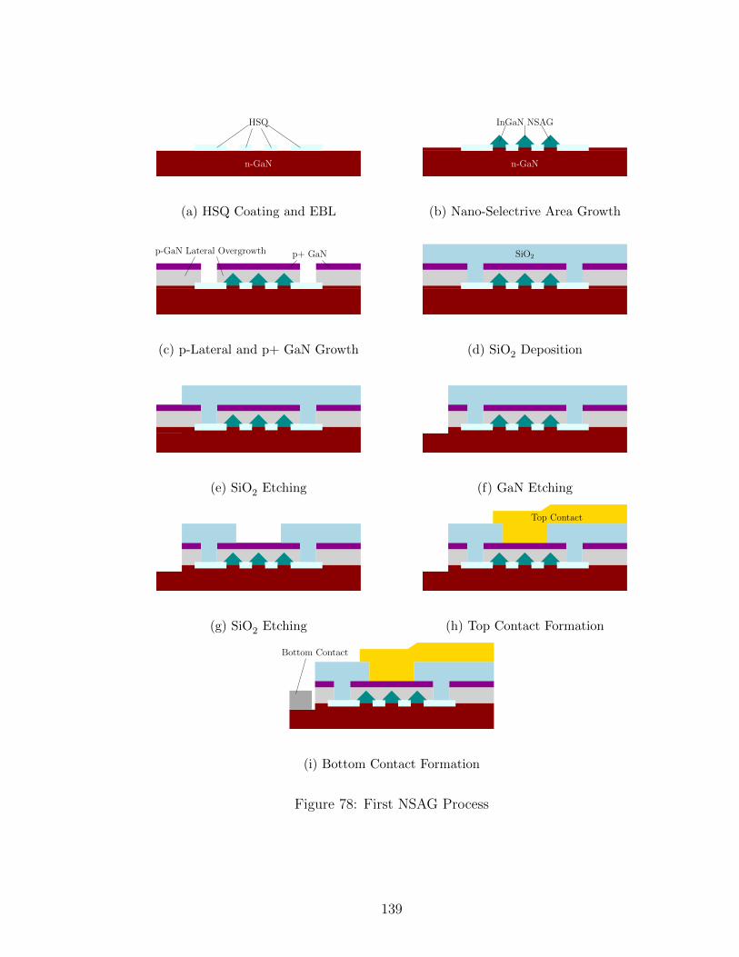
n-GaN
HSQ
(a) HSQ Coating and EBL
n-GaN
InGaN NSAG
(b) Nano-Selectrive Area Growth
p-GaN Lateral Overgrowth p+ GaN
(c) p-Lateral and p+ GaN Growth
SiO2
(d) SiO2
Deposition
(e) SiO2
Etching (f) GaN Etching
(g) SiO2
Etching
Top Contact
(h) Top Contact Formation
Bottom Contact
(i) Bottom Contact Formation
Figure 78: First NSAG Process
139
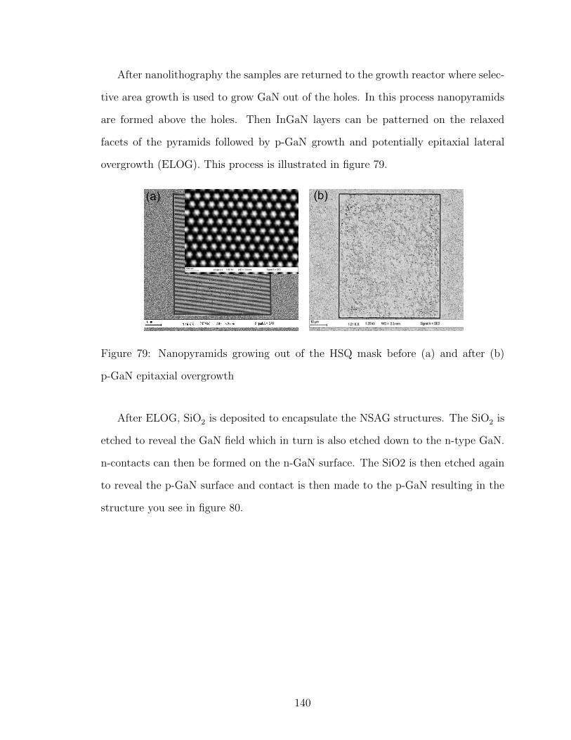
After nanolithography the samples are returned to the growth reactor where selec-
tive area growth is used to grow GaN out of the holes. In this process nanopyramids
are formed above the holes. Then InGaN layers can be patterned on the relaxed
facets of the pyramids followed by p-GaN growth and potentially epitaxial lateral
overgrowth (ELOG). This process is illustrated in figure 79.
(b) (a)
Figure 79: Nanopyramids growing out of the HSQ mask before (a) and after (b)
p-GaN epitaxial overgrowth
After ELOG, SiO2
is deposited to encapsulate the NSAG structures. The SiO2
is
etched to reveal the GaN field which in turn is also etched down to the n-type GaN.
n-contacts can then be formed on the n-GaN surface. The SiO2 is then etched again
to reveal the p-GaN surface and contact is then made to the p-GaN resulting in the
structure you see in figure 80.
140
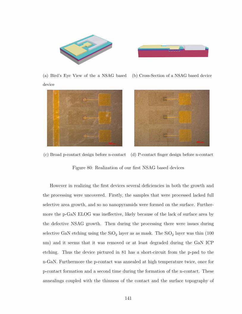
(a) Bird’s Eye View of the a NSAG based
device
(b) Cross-Section of a NSAG based device
(c) Broad p-contact design before n-contact (d) P-contact finger design before n-contact
Figure 80: Realization of our first NSAG based devices
However in realizing the first devices several deficiencies in both the growth and
the processing were uncovered. Firstly, the samples that were processed lacked full
selective area growth, and so no nanopyramids were formed on the surface. Further-
more the p-GaN ELOG was ine↵ective, likely because of the lack of surface area by
the defective NSAG growth. Then during the processing there were issues during
selective GaN etching using the SiO2
layer as as mask. The SiO2
layer was thin (100
nm) and it seems that it was removed or at least degraded during the GaN ICP
etching. Thus the device pictured in 81 has a short-circuit from the p-pad to the
n-GaN. Furthermore the p-contact was annealed at high temperature twice, once for
p-contact formation and a second time during the formation of the n-contact. These
annealings coupled with the thinness of the contact and the surface topography of
141
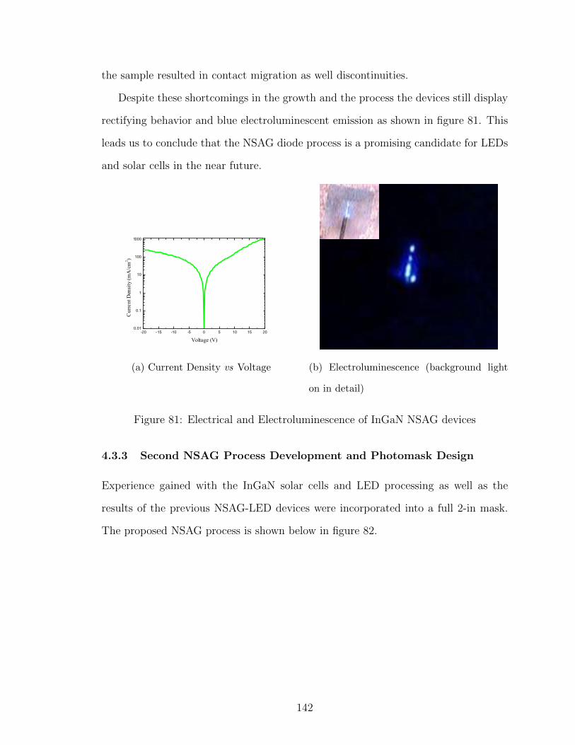
the sample resulted in contact migration as well discontinuities.
Despite these shortcomings in the growth and the process the devices still display
rectifying behavior and blue electroluminescent emission as shown in figure 81. This
leads us to conclude that the NSAG diode process is a promising candidate for LEDs
and solar cells in the near future.
-20 -15 -10 -5 0 5 10 15 200.01
0.1
1
10
100
1000
Cur
rent
Den
sity
(mA
/cm
2 )
Voltage (V)
(a) Current Density vs Voltage (b) Electroluminescence (background light
on in detail)
Figure 81: Electrical and Electroluminescence of InGaN NSAG devices
4.3.3 Second NSAG Process Development and Photomask Design
Experience gained with the InGaN solar cells and LED processing as well as the
results of the previous NSAG-LED devices were incorporated into a full 2-in mask.
The proposed NSAG process is shown below in figure 82.
142
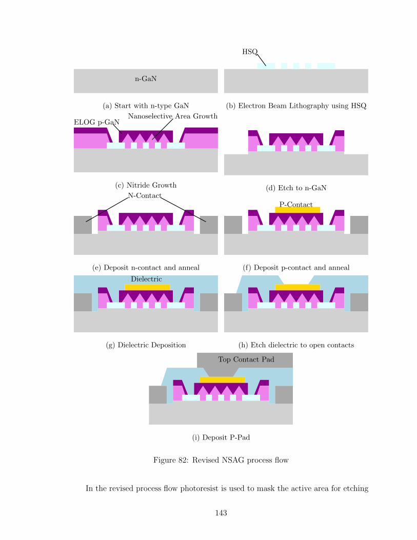
n-GaN
(a) Start with n-type GaN
HSQ
(b) Electron Beam Lithography using HSQ
Nanoselective Area GrowthELOG p-GaN
(c) Nitride Growth (d) Etch to n-GaNN-Contact
(e) Deposit n-contact and anneal
P-Contact
(f) Deposit p-contact and anneal
Dielectric
(g) Dielectric Deposition (h) Etch dielectric to open contacts
Top Contact Pad
(i) Deposit P-Pad
Figure 82: Revised NSAG process flow
In the revised process flow photoresist is used to mask the active area for etching
143
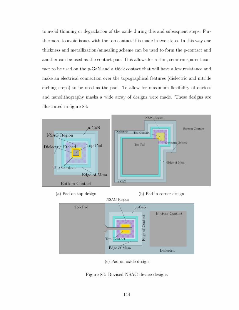
to avoid thinning or degradation of the oxide during this and subsequent steps. Fur-
thermore to avoid issues with the top contact it is made in two steps. In this way one
thickness and metallization/annealing scheme can be used to form the p-contact and
another can be used as the contact pad. This allows for a thin, semitransparent con-
tact to be used on the p-GaN and a thick contact that will have a low resistance and
make an electrical connection over the topographical features (dielectric and nitride
etching steps) to be used as the pad. To allow for maximum flexibility of devices
and nanolithography masks a wide array of designs were made. These designs are
illustrated in figure 83.
Bottom Contact
n-GaN
Top Contact
Edge of Mesa
NSAG Region
Dielectric Etched Top Pad
(a) Pad on top design
Bottom Contact
NSAG Region
Edge of Mesa
Dielectric
Dielectric Etched
Top Contact
Top Pad
n-GaN
(b) Pad in corner design
Bottom Contact
Dielectric
NSAG Region
Top Contact
Edge of Mesa
Top Pad
Edge
ofC
onta
ct
n-GaN
(c) Pad on oxide design
Figure 83: Revised NSAG device designs
144

The various designs alter both the size of the NSAG region as well as the place-
ment and design of the top contact pad in order to allow the maximum freedom for
nanolithography masks. To date these devices have not been realized, but progress
is being made and the first results are expected in the next 4 to 6 months.
145
CHAPTER V
CONCLUSIONS AND FUTURE WORK
Solar cells will be one of many technologies used for producing electricity in the 21st
century whether by large, utility-scale solar plants, small distributed power generation
on residential and commercial buildings, or in outer space. We have described both
the economic pressures driving innovation in solar cell research and advancements in
materials and technology that are opening new avenues of research for high e�ciency
solar cells.
One such advancement was the revision of the band gap energy of InN down to 0.8
eV. Now InGaN appears to be a likely candidate for high performing solar cells, espe-
cially when combined in tandem with a lower cost solar cell material like Si. However,
many challenges are blocking InGaN from reaching its theoretical maximum poten-
tial. Firstly the growth of reproducible, thick, high quality, high In content InGaN
has yet to be achieved. Our laboratory has made significant strides in this regard
by demonstrating both semibulk and nanoselective area growth approaches. Further
di�culties with the number of material defects in InGaN materials caused in no small
part by the lack of lattice matched substrates adversely e↵ect the solar cell perfor-
mance. Again nanoselective area growth combined with lateral epitaxy methods can
reduce the e↵ect of this issue. Lastly a double heterojunction (p-GaN/InGaN/n-
GaN), approach has proved the most fruitful in the production of InGaN based solar
cells. To implement this approach using MOVPE technology a compromise must be
made between the InGaN absorber layer quality and the p-GaN morphology. We
have shown that using low-temperature p-GaN it is possible to achieve a high quality
InGaN absorber, but with v-pits in the p-GaN. These v-pits can enhance the short
146
circuit current of a solar cell, if included as grown into a final device the solar cell
performance is reduced due to a high leakage current. We have shown a promising
technology using HSQ resin to passivate the v-pits, thus maintaining both the ab-
sorber quality during p-GaN growth and the short circuit enhancement caused by the
v-pits.
We have demonstrated the solar cell processing on LEDs and have optimized
many of the processing steps. This work has greatly reduced the series resistance
and repeatability of the LED devices. Further work needs to be done in studying the
p-contacts, mesa passivation, and anti-reflection coatings, but the work has resulted
in working InGaN/Si tandem solar cells.
147
REFERENCES
[1] A. Sreedhar, B. Sharma, and R. Purohit, “E�ciency calculations of heterojunc-tion solar energy converters,” IEEE Transactions on Electron Devices, vol. 16,no. 3, pp. 309–312, 1969.
[2] K. Pantzas, Elaboration par MOVPE et caracterisation des materiaux(B)InGaN pour les cellules solaires de 3eme generation. PhD thesis, Universitede Lorraine, 2013.
[3] J. Piprek, Semiconductor optoelectronic devices: introduction to physics andsimulation. Academic Press, 2013.
[4] A. Bhuiyan, K. Sugita, A. Hashimoto, and A. Yamamoto, “Ingan solar cells:present state of the art and important challenges,” Photovoltaics, IEEE Journalof, vol. 2, no. 3, pp. 276–293, 2012.
[5] G. Greco, F. Iucolano, and F. Roccaforte, “Ohmic contacts to gallium nitridematerials,” Applied Surface Science, vol. 383, pp. 324–345, 2016.
[6] A. Standard, “G159, standard tables for references solar spectral irradiance atair mass 1.5: Direct normal and hemispherical for a 37 tilted surface,” Societyfor Testing Matls., West Conshocken, PA, USA, 1998.
[7] M. Razeghi, Fundamentals of solid state engineering. Springer Science & Busi-ness Media, 2009.
[8] U. E. I. Administration, “Levelized cost and levelized avoided cost of new gen-eration resources in the annual energy outlook 2016,” 2015.
[9] Cadmium, “Pervoskite lattice,” 2006. https://commons.wikimedia.org/
wiki/File:Perovskite.jpg,, [Accessed 25-December-2016].
[10] B. M. Kayes, L. Zhang, R. Twist, I.-K. Ding, and G. S. Higashi, “Flexible thin-film tandem solar cells with > 30% e�ciency,” IEEE Journal of Photovoltaics,vol. 4, no. 2, pp. 729–733, 2014.
[11] S. Moon, K. Kim, Y. Kim, J. Heo, and J. Lee, “Highly e�cient single-junctiongaas thin-film solar cell on flexible substrate,” Scientific Reports, vol. 6, 2016.
[12] A. Barnett, C. Honsberg, D. Kirkpatrick, S. Kurtz, D. Moore, D. Salzman,R. Schwartz, J. Gray, S. Bowden, K. Goossen, et al., “50% e�cient solar cellarchitectures and designs,” in 2006 IEEE 4th World Conference on PhotovoltaicEnergy Conference, vol. 2, pp. 2560–2564, IEEE, 2006.
148
[13] M. Arif, W. Elhuni, J. Streque, S. Sundaram, S. Belahsene, Y. El Gmili, M. Jor-dan, X. Li, G. Patriarche, A. Slaoui, et al., “Improving ingan heterojunctionsolar cells e�ciency using a semibulk absorber,” Solar Energy Materials andSolar Cells, vol. 159, pp. 405–411, 2017.
[14] W. El-Huni, A. Migan, Z. Djebbour, J.-P. Salvestrini, and A. Ougazzaden,“High-e�ciency indium gallium nitride/si tandem photovoltaic solar cells mod-eling using indium gallium nitride semibulk material: monolithic integrationversus 4-terminal tandem cells,” Progress in Photovoltaics: Research and Ap-plications, vol. 24, no. 11, pp. 1436–1447, 2016. PIP-15-226.R2.
[15] M. Arif, J.-P. Salvestrini, J. Streque, M. B. Jordan, Y. El Gmili, S. Sundaram,X. Li, G. Patriarche, P. L. Voss, and A. Ougazzaden, “Role of v-pits in theperformance improvement of ingan solar cells,” Applied Physics Letters, 2016.
[16] C. Holzwarth, T. Barwicz, and H. I. Smith, “Optimization of hydrogensilsesquioxane for photonic applications,” Journal of Vacuum Science & Tech-nology B, vol. 25, no. 6, pp. 2658–2661, 2007.
[17] H.-C. Liou and J. Pretzer, “E↵ect of curing temperature on the mechanicalproperties of hydrogen silsesquioxane thin films,” Thin Solid Films, vol. 335,no. 1, pp. 186–191, 1998.
[18] R. Baillot, Methodologie d’analyse de defaillance pour l’evaluation de la fia-bilite de diodes electroluminescentes GaN. PhD thesis, Universite Sciences etTechnologies-Bordeaux I, 2011.
[19] B. Chambion, Etude de la fiabilite de modules a base de LEDs blanches pourapplications automobile. PhD thesis, Universite de Bordeaux, 2014.
[20] M. A. Green, “Silicon solar cells: state of the art,” Philosophical Transactionsof the Royal Society of London A: Mathematical, Physical and EngineeringSciences, vol. 371, no. 1996, p. 20110413, 2013.
[21] L. Hsu and W. Walukiewicz, “Modeling of InGaN/Si tandem solar cells,” Jour-nal of Applied Physics, vol. 104, no. 2, p. 024507, 2008.
[22] C. E. Backus, Solar cells. Institute of Electrical & Electronics Engineers(IEEE),1976.
[23] J. Parrott, “Radiative recombination and photon recycling in photovoltaic solarcells,” Solar energy materials and solar cells, vol. 30, no. 3, pp. 221–231, 1993.
[24] S. R. Wenham, Applied photovoltaics. Routledge, 2012.
[25] M. M. de Wild-Scholten, “Energy payback time and carbon footprint of com-mercial photovoltaic systems,” Solar Energy Materials and Solar Cells, vol. 119,pp. 296–305, 2013.
149
[26] I. Fraunhofer, “Photovoltaics report, updated november 11, 2016,” FraunhoferISE, Freiburg, 2016.
[27] M. de Wild-Scholten, M. Sturm, M. Butturi, M. Noack, and K. Heasman, “En-vironmental sustainability of concentrator pv systems: preliminary lca resultsof the apollon project,” in 5th World Conference on Photovoltaic Energy Con-version Valencia. Spain, pp. 6–10, 2010.
[28] A. De Vos, “Detailed balance limit of the e�ciency of tandem solar cells,”Journal of Physics D: Applied Physics, vol. 13, no. 5, p. 839, 1980.
[29] S. A. Campbell, S. A. Campbell, and A. C. Stephen, Fabrication engineeringat the micro-and nanoscale. No. Sirsi) i9780195320176, 2008.
[30] J. Zhao, A. Wang, and M. A. Green, “High-e�ciency perl and pert silicon solarcells on fz and mcz substrates,” Solar Energy Materials and Solar Cells, vol. 65,no. 1, pp. 429–435, 2001.
[31] P. Campbell and M. A. Green, “Light trapping properties of pyramidally tex-tured surfaces,” Journal of Applied Physics, vol. 62, no. 1, pp. 243–249, 1987.
[32] J. Benick, B. Steinhauser, R. Muller, J. Bartsch, M. Kamp, A. Mondon,A. Richter, M. Hermle, and S. Glunz, “High e�ciency n-type pert and perlsolar cells,” in 2014 IEEE 40th Photovoltaic Specialist Conference (PVSC),pp. 3637–3640, IEEE, 2014.
[33] D. Jordan and J. Nagle, “Buried contact concentrator solar cells,” Progress inPhotovoltaics: Research and Applications, vol. 2, pp. 171–176, 1994.
[34] J. Wohlgemuth and S. Narayanan, “Buried contact concentrator solar cells,”in Photovoltaic Specialists Conference, 1991., Conference Record of the TwentySecond IEEE, pp. 273–277, IEEE, 1991.
[35] H. C. Card and E. S. Yang, “Electronic processes at grain boundaries in poly-crystalline semiconductors under optical illumination,” IEEE Transactions onElectron Devices, vol. 24, no. 4, pp. 397–402, 1977.
[36] W. Paul and D. A. Anderson, “Properties of amorphous hydrogenated silicon,with special emphasis on preparation by sputtering,” Solar Energy Materials,vol. 5, no. 3, pp. 229–316, 1981.
[37] A. Shah, J. Meier, A. Buechel, U. Kroll, J. Steinhauser, F. Meillaud, H. Schade,and D. Domine, “Towards very low-cost mass production of thin-film siliconphotovoltaic (pv) solar modules on glass,” Thin Solid Films, vol. 502, no. 1,pp. 292–299, 2006.
[38] A. Shah, P. Torres, R. Tscharner, N. Wyrsch, and H. Keppner, “Photovoltaictechnology: the case for thin-film solar cells,” science, vol. 285, no. 5428,pp. 692–698, 1999.
150

[39] M. A. Green, K. Emery, Y. Hishikawa, W. Warta, and E. D. Dunlop, “So-lar cell e�ciency tables (version 45),” Progress in photovoltaics: research andapplications, vol. 23, no. 1, pp. 1–9, 2015.
[40] U. S. G. Survey, “Tellerium,” Mineral Commodity Summaries, 2008.
[41] N. R. E. Centre, “First solar cdte photovoltaic technology: Environmental,health and safety assessment,” Published Online, 2013.
[42] M. Marwede and A. Reller, “Future recycling flows of tellurium from cadmiumtelluride photovoltaic waste,” Resources, Conservation and Recycling, vol. 69,pp. 35–49, 2012.
[43] K. Zweibel, “Thin film pv manufacturing: Materials costs and their optimiza-tion,” Solar energy materials and solar cells, vol. 63, no. 4, pp. 375–386, 2000.
[44] J. Kalowekamo and E. Baker, “Estimating the manufacturing cost of purelyorganic solar cells,” Solar Energy, vol. 83, no. 8, pp. 1224–1231, 2009.
[45] M. Kemell, M. Ritala, and M. Leskela, “Thin film deposition methods for cuinse2 solar cells,” Critical Reviews in Solid State and Materials Sciences, vol. 30,no. 1, pp. 1–31, 2005.
[46] T. Klinkert, M. Jubault, F. Donsanti, D. Lincot, and J.-F. Guillemoles, “Gagradients in cu (in, ga) se2: Formation, characterization, and consequences,”Journal of Renewable and Sustainable Energy, vol. 6, no. 1, p. 011403, 2014.
[47] M. Konagai, M. Sugimoto, and K. Takahashi, “High e�ciency gaas thin filmsolar cells by peeled film technology,” Journal of crystal growth, vol. 45, pp. 277–280, 1978.
[48] M. Gratzel, “Dye-sensitized solar cells,” Journal of Photochemistry and Photo-biology C: Photochemistry Reviews, vol. 4, no. 2, pp. 145–153, 2003.
[49] A. Kojima, K. Teshima, Y. Shirai, and T. Miyasaka, “Organometal halide per-ovskites as visible-light sensitizers for photovoltaic cells,” Journal of the Amer-ican Chemical Society, vol. 131, no. 17, pp. 6050–6051, 2009.
[50] M. M. Lee, J. Teuscher, T. Miyasaka, T. N. Murakami, and H. J. Snaith,“E�cient hybrid solar cells based on meso-superstructured organometal halideperovskites,” Science, vol. 338, no. 6107, pp. 643–647, 2012.
[51] C. H. Henry, “Limiting e�ciencies of ideal single and multiple energy gap ter-restrial solar cells,” Journal of applied physics, vol. 51, no. 8, pp. 4494–4500,1980.
[52] P. Rappaport, “The photovoltaic e↵ect and its utilization1 rca rev. 20, 373-397,”1959.
151
[53] R. Anderson, “Experiments on ge-gaas heterojunctions,” in Electronic Structureof Semiconductor Heterojunctions, pp. 35–48, Springer, 1988.
[54] “Alta devices achieves 31.6% solar energy e�ciency record; changes the funda-mental economics for unmanned aerial vehicles.” Accessed: 2016-12-17.
[55] E. Jackson, “Areas for improvement of the semiconductor solar energy con-verter,” in Transactions of the Conference on the Use of Solar Energy, vol. 5,pp. 122–126, 1955.
[56] P. Chiu, D. Law, R. Woo, S. Singer, D. Bhusari, W. Hong, A. Zakaria,J. Boisvert, S. Mesropian, R. King, et al., “Direct semiconductor bonded 5j cellfor space and terrestrial applications,” IEEE Journal of Photovoltaics, vol. 4,no. 1, pp. 493–497, 2014.
[57] H. Serreze, “Optimizing solar cell performance by simultaneous considerationof grid pattern design and interconnect configuration,” in 13th PhotovoltaicSpecialists Conference, vol. 1, pp. 609–614, 1978.
[58] L. Vegard, “Die konstitution der mischkristalle und die raumfullung der atome,”Zeitschrift fur Physik A Hadrons and Nuclei, vol. 5, no. 1, pp. 17–26, 1921.
[59] A. R. Denton and N. W. Ashcroft, “Vegard?s law,” Physical review A, vol. 43,no. 6, p. 3161, 1991.
[60] O. K. Jani, “Development of wide-band gap ingan solar cells for high-e�ciencyphotovoltaics,” 2008.
[61] J. Wu, W. Walukiewicz, K. Yu, J. Ager III, E. Haller, H. Lu, and W. J.Scha↵, “Small band gap bowing in in1axgaxn alloys,” Appl. Phys. Lett, vol. 80,pp. 4741–4743, 2002.
[62] M. Hori, K. Kano, T. Yamaguchi, Y. Saito, T. Araki, Y. Nanishi, N. Teraguchi,and A. Suzuki, “Optical properties of inxga1?xn with entire alloy compositionon inn bu↵er layer grown by rf-mbe,” physica status solidi (b), vol. 234, no. 3,pp. 750–754, 2002.
[63] R. Singh, D. Doppalapudi, T. Moustakas, and L. Romano, “Phase separationin ingan thick films and formation of ingan/gan double heterostructures in theentire alloy composition,” Applied Physics Letters, vol. 70, no. 9, pp. 1089–1091,1997.
[64] H. Angerer, O. Ambacher, R. Dimitrov, T. Metzger, W. Rieger, and M. Stutz-mann, “PEMBE-growth of gallium nitride on (0001) sapphire: A comparisonto MOCVD grown GaN,” MRS Internet Journal of Nitride Semiconductor Re-search, vol. 1, p. e15, 1996.
152

[65] T. Hashimoto, F. Wu, J. S. Speck, and S. Nakamura, “A GaN bulk crystal withimproved structural quality grown by the ammonothermal method,” Naturematerials, vol. 6, no. 8, pp. 568–571, 2007.
[66] D. Holec, Y. Zhang, D. S. Rao, C. Kappers, Menno J achnd McAleese, andC. J. Humphreys, “Equilibrium critical thickness for misfit dislocations in III-nitrides,” Journal of Applied Physics, vol. 104, no. 12, p. 123514, 2008.
[67] C. Hemmingsson, P. Paskov, G. Pozina, M. Heuken, B. Schineller, and B. Mon-emar, “Growth of bulk gan in a vertical hydride vapour phase epitaxy reactor,”Superlattices and Microstructures, vol. 40, no. 4, pp. 205–213, 2006.
[68] I.-h. Ho and G. Stringfellow, “Solid phase immiscibility in gainn,” AppliedPhysics Letters, vol. 69, no. 18, pp. 2701–2703, 1996.
[69] M. Ichimura and A. Sasaki, “Short-range order in iii-v ternary alloy semicon-ductors,” Journal of applied physics, vol. 60, no. 11, pp. 3850–3855, 1986.
[70] S. Y. Karpov, “Suppression of phase separation in InGaN due to elastic strain,”MRS Internet Journal of Nitride Semiconductor Research, vol. 3, p. e16, 1998.
[71] K. Pantzas, Y. El Gmili, J. Dickerson, S. Gautier, L. Largeau, O. Mauguin,G. Patriarche, S. Suresh, T. Moudakir, C. Bishop, et al., “Semibulk InGaN:A novel approach for thick, single phase, epitaxial InGaN layers grown byMOVPE,” Journal of Crystal Growth, vol. 370, pp. 57–62, 2013.
[72] R. Puybaret, G. Patriache, M. B. Jordan, S. Sundaram, Y. el Gmili, J.-P.Salvestrini, P. L. Voss, W. A. de Heer, C. Berger, and A. Ougazzaden, “Nanos-elective area growth of GaN by metalorganic vapor phase epitaxy on 4H-SiC us-ing epitaxial graphene as a mask,” Applied Physics Letters, vol. 108, pp. 103105–103105–5, 2016.
[73] S. Strite and H. Morkoc, “Gan, aln, and inn: a review,” Journal of VacuumScience & Technology B, vol. 10, no. 4, pp. 1237–1266, 1992.
[74] H. Amano, M. Kito, K. Hiramatsu, and I. Akasaki, “P-type conduction in mg-doped gan treated with low-energy electron beam irradiation (leebi),” JapaneseJournal of Applied Physics, vol. 28, no. 12A, p. L2112, 1989.
[75] S. Nakamura, M. Senoh, and T. Mukai, “Highly p-typed mg-doped gan filmsgrown with gan bu↵er layers,” Japanese journal of applied physics, vol. 30,no. 10A, p. L1708, 1991.
[76] Y. Guo, X. Liu, H. Song, A. Yang, X. Xu, G. Zheng, H. Wei, S. Yang, Q. Zhu,and Z. Wang, “A study of indium incorporation in In-rich InGaN grown byMOVPE,” Applied Surface Science, vol. 256, no. 10, pp. 3352–3356, 2010.
153
[77] C. A. Fabien and W. A. Doolittle, “Guidelines and limitations for the designof high-e�ciency ingan single-junction solar cells,” Solar Energy Materials andSolar Cells, vol. 130, pp. 354–363, 2014.
[78] T. Wang, T. Ciszek, C. Schwerdtfeger, H. Moutinho, and R. Matson, “Growthof silicon thin layers on cast mg si from metal solutions for solar cells,” Solarenergy materials and solar cells, vol. 41, pp. 19–30, 1996.
[79] O. Jani, H. Yu, E. Trybus, B. Jampana, I. Ferguson, A. Doolittle, and C. Hons-berg, “E↵ect of phase separation on performance of III-V nitride solar cells,”in 22nd European Photovoltaic Solar Energy Conference, pp. 3–7, 2007.
[80] J. Wu, W. Walukiewicz, K. Yu, W. Shan, J. Ager Iii, E. Haller, H. Lu, W. J.Scha↵, W. Metzger, and S. Kurtz, “Superior radiation resistance of in1- xgaxnalloys: Full-solar-spectrum photovoltaic material system,” Journal of AppliedPhysics, vol. 94, no. 10, pp. 6477–6482, 2003.
[81] A. Mukhtarova, Puits quantiques de composes nitrures InGaN/GaN pour lephotovaoltaique. PhD thesis, Grenoble Alpes, 2015.
[82] X. Cai, Y. Wang, B. Chen, M.-M. Liang, W.-J. Liu, J.-Y. Zhang, X.-Q. Lv,L.-Y. Ying, and B.-P. Zhang, “Investigation of InGaN pin homojunction andheterojunction solar cells,” IEEE Photonics technology letters, vol. 25, no. 1,pp. 59–62, 2013.
[83] C. Yang, X. Wang, H. Xiao, J. Ran, C. Wang, G. Hu, X. Wang, X. Zhang,J. Li, and J. Li, “Photovoltaic e↵ects in InGaN structures with p–n junctions,”physica status solidi (a), vol. 204, no. 12, pp. 4288–4291, 2007.
[84] O. Jani, B. Jampana, M. Mehta, H. Yu, I. Ferguson, R. Opila, and C. Hons-berg, “Optimization of GaN window layer for InGaN solar cells using polariza-tion e↵ect,” in Photovoltaic Specialists Conference, 2008. PVSC’08. 33rd IEEE,pp. 1–4, IEEE, 2008.
[85] A. Yamamoto, M. R. Islam, T.-T. Kang, and A. Hashimoto, “Recent advancesin InN-based solar cells: status and challenges in InGaN and InAlN solar cells,”physica status solidi (c), vol. 7, no. 5, pp. 1309–1316, 2010.
[86] A. Yamamoto, K. Sugita, M. Horie, Y. Ohmura, M. R. Islam, and A. Hashimoto,“Mg-doping and n+-p junction formation in MOVPE-grown InxGa
1�xn(x 0.4),” in Photovoltaic Specialists Conference, 2008. PVSC’08. 33rd IEEE,pp. 1–3, IEEE, 2008.
[87] B. R. Jampana, A. G. Melton, M. Jamil, N. N. Faleev, R. L. Opila, I. T.Ferguson, and C. B. Honsberg, “Design and realization of wide-band-gap (2.67eV) InGaN pn junction solar cell,” Electron Device Letters, IEEE, vol. 31, no. 1,pp. 32–34, 2010.
154

[88] P. Misra, C. Boney, N. Medelci, D. Starikov, A. Freundlich, and A. Bensaoula,“Fabrication and characterization of 2.3 eV InGaN photovoltaic devices,” inPhotovoltaic Specialists Conference, 2008. PVSC’08. 33rd IEEE, pp. 1–5, IEEE,2008.
[89] C. Boney, I. Hernandez, R. Pillai, D. Starikov, A. Bensaoula, M. Henini,M. Syperek, J. Misiewicz, and R. Kudrawiec, “Growth and characterizationof InGaN for photovoltaic devices,” in Photovoltaic Specialists Conference(PVSC), 2010 35th IEEE, pp. 003316–003321, IEEE, 2010.
[90] X. Cai, S. Zeng, and B.-P. Zhang, “Favourable photovoltaic e↵ects in InGaNpin homojunction solar cell,” Electronics letters, vol. 45, no. 24, p. 1, 2009.
[91] X. Chen, K. Matthews, D. Hao, W. Scha↵, and L. Eastman, “Growth, fab-rication, and characterization of InGaN solar cells,” physica status solidi (a),vol. 205, no. 5, pp. 1103–1105, 2008.
[92] X. Chen, K. Matthews, D. Hao, W. Scha↵, L. Eastman, W. Walukiewicz, J. Age,and K. Yu, “Characterization of Mg-doped InGaN and InAlN alloys grownby MBE for solar applications,” in Photovoltaic Specialists Conference, 2008.PVSC’08. 33rd IEEE, pp. 1–6, IEEE, 2008.
[93] R. Dahal, B. Pantha, J. Li, J. Lin, and H. Jiang, “InGaN/GaN multiple quan-tum well solar cells with long operating wavelengths,” Applied Physics Letters,vol. 94, no. 6, p. 063505, 2009.
[94] M.-J. Jeng, Y.-L. Lee, and L.-B. Chang, “Temperature dependences ofInxGa1 � xN multiple quantum well solar cells,” Journal of Physics D: AppliedPhysics, vol. 42, no. 10, p. 105101, 2009.
[95] K. Lai, G. Lin, Y. Lai, Y. Chen, and J. He, “E↵ect of indium fluctuation on thephotovoltaic characteristics of InGaN/GaN multiple quantum well solar cells,”Applied Physics Letters, vol. 96, no. 8, p. 081103, 2010.
[96] R. Dahal, J. Li, K. Aryal, J. Lin, and H. Jiang, “InGaN/GaN multiple quantumwell concentrator solar cells,” Appl. Phys. Lett, vol. 97, no. 7, p. 073115, 2010.
[97] Y.-J. Lee, M.-H. Lee, C.-M. Cheng, and C.-H. Yang, “Enhanced conversione�ciency of InGaN multiple quantum well solar cells grown on a patternedsapphire substrate,” Applied Physics letters, vol. 98, no. 26, p. 263504, 2011.
[98] J.-K. Sheu, C.-C. Yang, S.-J. Tu, K.-H. Chang, M.-L. Lee, W.-C. Lai, and L.-C.Peng, “Demonstration of GaN-based solar cells with GaN/ InGaN superlatticeabsorption layers,” Electron Device Letters, IEEE, vol. 30, no. 3, pp. 225–227,2009.
[99] B. W. Liou, “InGaN–GaN–based solar cells with a multiple-quantum-well struc-ture on SiCN–Si (111) substrates,” Photonics Technology Letters, IEEE, vol. 22,no. 4, pp. 215–217, 2010.
155
[100] C. Yang, J. Sheu, X.-W. Liang, M.-S. Huang, M. Lee, K. Chang, S. Tu, F.-W.Huang, and W. Lai, “Enhancement of the conversion e�ciency of GaN-basedphotovoltaic devices with AlGaN/ InGaN absorption layers,” Appl. Phys. Lett,vol. 97, no. 2, p. 021113, 2010.
[101] Y. Kuwahara, T. Fujii, T. Sugiyama, D. Iida, Y. Isobe, Y. Fujiyama, Y. Morita,M. Iwaya, T. Takeuchi, S. Kamiyama, et al., “GaInN-based solar cells usingstrained-layer GaInN/GaInN superlattice active layer on a freestanding GaNsubstrate,” Applied physics express, vol. 4, no. 2, p. 021001, 2011.
[102] O. Jani, I. Ferguson, C. Honsberg, and S. Kurtz, “Design and characterizationof GaN/ InGaN solar cells,” Applied Physics Letters, vol. 91, no. 13, p. 132117,2007.
[103] C. J. Neufeld, N. G. Toledo, S. C. Cruz, M. Iza, S. P. DenBaars, and U. K.Mishra, “High quantum e�ciency InGaN/GaN solar cells with 2.95 eV bandgap,” Applied Physics Letters, vol. 93, no. 14, p. 3502, 2008.
[104] X. Zheng, R.-H. Horng, D.-S. Wuu, M.-T. Chu, W.-Y. Liao, M.-H. Wu, R.-M. Lin, and Y.-C. Lu, “High-quality InGaN/GaN heterojunctions and theirphotovoltaic e↵ects,” Applied Physics Letters, vol. 93, no. 26, p. 261108, 2008.
[105] R.-H. Horng, S.-T. Lin, Y.-L. Tsai, M.-T. Chu, W.-Y. Liao, M.-H. Wu, R.-M.Lin, and Y.-C. Lu, “Improved conversion e�ciency of GaN/ InGaN thin-filmsolar cells,” Electron Device Letters, IEEE, vol. 30, no. 7, pp. 724–726, 2009.
[106] C.-L. Tsai, G.-S. Liu, G.-C. Fan, and Y.-S. Lee, “Substrate-free large gap InGaNsolar cells with bottom reflector,” Solid-State Electronics, vol. 54, no. 5, pp. 541–544, 2010.
[107] Y. Kuwahara, T. Fujii, Y. Fujiyama, T. Sugiyama, M. Iwaya, T. Takeuchi,S. Kamiyama, I. Akasaki, and H. Amano, “Realization of nitride-based solarcell on freestanding GaN substrate,” Applied physics express, vol. 3, no. 11,p. 111001, 2010.
[108] E. Matioli, C. Neufeld, M. Iza, S. C. Cruz, A. A. Al-Heji, X. Chen, R. M.Farrell, S. Keller, S. DenBaars, U. Mishra, et al., “High internal and externalquantum e�ciency InGaN/GaN solar cells,” Applied Physics Letters, vol. 98,no. 2, p. 021102, 2011.
[109] H. C. Lee, Y. K. Su, W. H. Lan, J. C. Lin, K. C. Huang, W. J. Lin, Y. C. Cheng,and Y. H. Yeh, “Study of electrical characteristics of GaN-based photovoltaicswith graded in ga n absorption layer,” Photonics Technology Letters, IEEE,vol. 23, no. 6, pp. 347–349, 2011.
[110] J.-P. Shim, M. Choe, S.-R. Jeon, D. Seo, T. Lee, and D.-S. Lee, “InGaN-basedp–i–n solar cells with graphene electrodes,” Applied physics express, vol. 4, no. 5,p. 052302, 2011.
156
[111] J. Lang, C. Neufeld, C. Hurni, S. Cruz, E. Matioli, U. Mishra, and J. Speck,“High external quantum e�ciency and fill-factor InGaN/GaN heterojunctionsolar cells grown by NH
3
-based molecular beam epitaxy,” Applied Physics Let-ters, vol. 98, 2011.
[112] G. Zhang, Y. Tong, Z. Yang, S. Jin, J. Li, and Z. Gan, “Relationship of back-ground carrier concentration and defects in GaN grown by metalorganic vaporphase epitaxy,” Applied physics letters, vol. 71, no. 23, pp. 3376–3378, 1997.
[113] S. Heikman, S. Keller, S. P. DenBaars, and U. K. Mishra, “Growth of Fedoped semi-insulating GaN by metalorganic chemical vapor deposition,” Ap-plied Physics Letters, vol. 81, no. 3, pp. 439–441, 2002.
[114] W. Lee, J.-H. Ryou, D. Yoo, J. Limb, R. D. Dupuis, D. Hanser, E. Preble,M. N. Williams, and K. Evans, “Optimization of Fe doping at the regrowthinterface of GaN for applications to III-nitride-based heterostructure field-e↵ecttransistors,” Applied Physics Letters, vol. 90, no. 9, p. 09509, 2007.
[115] A. Castiglia, J.-F. Carlin, and N. Grandjean, “Role of stable and metastableMg–H complexes in p-type GaN for cw blue laser diodes,” Applied PhysicsLetters, vol. 98, no. 21, p. 213505, 2011.
[116] C. G. Van de Walle, “Interactions of hydrogen with native defects in GaN,”Physical Review B, vol. 56, no. 16, p. R10020, 1997.
[117] L. Dobos, B. Pecz, L. Toth, Z. J. Horvath, Z. Horvath, A. Toth, E. Horvath,B. Beaumont, and Z. Bougrioua, “Metal contacts to n-GaN,” Applied SurfaceScience, vol. 253, no. 2, pp. 655–661, 2006.
[118] A. Schmitz, A. Ping, M. A. Khan, Q. Chen, J. Yang, and I. Adesida, “Metalcontacts to n-type GaN,” Journal of Electronic Materials, vol. 27, no. 4, pp. 255–260, 1998.
[119] H. L. Skriver and N. Rosengaard, “Surface energy and work function of elemen-tal metals,” Physical Review B, vol. 46, no. 11, p. 7157, 1992.
[120] B. Luther, S. Mohney, T. Jackson, M. A. Khan, Q. Chen, and J. Yang, “Investi-gation of the mechanism for ohmic contact formation in Al and Ti/Al contactsto n-type GaN,” Applied physics letters, vol. 70, no. 1, pp. 57–59, 1997.
[121] Y. Lin, S.-J. Chang, Y.-K. Su, T.-Y. Tsai, C. Chang, S.-C. Shei, C. Kuo, andS. Chen, “InGaN/GaN light emitting diodes with Ni/Au, Ni/ITO and ITOp-type contacts,” Solid-State Electronics, vol. 47, no. 5, pp. 849–853, 2003.
[122] J. Sheu, Y.-K. Su, G.-C. Chi, P. Koh, M. Jou, C. Chang, C. Liu, and W. Hung,“High-transparency Ni/Au ohmic contact to p-type GaN,” Applied physics let-ters, vol. 74, no. 16, pp. 2340–2342, 1999.
157
[123] J. Smalc-Koziorowska, S. Grzanka, E. Litwin-Staszewska, R. Piotrzkowski,G. Nowak, M. Leszczynski, P. Perlin, E. Talik, J. Kozubowski, andS. Krukowski, “Ni–Au contacts to p-type GaN–structure and properties,” Solid-State Electronics, vol. 54, no. 7, pp. 701–709, 2010.
[124] X. Cao, S. Pearton, A. Zhang, G. Dang, F. Ren, R. Shul, L. Zhang, R. Hickman,and J. Van Hove, “Electrical e↵ects of plasma damage in p-GaN,” Appliedphysics letters, vol. 75, no. 17, 1999.
[125] N. Young, E. Perl, R. Farrell, M. Iza, S. Keller, J. Bowers, S. Nakamura,S. DenBaars, and J. Speck, “High-performance broadband optical coatings oningan/gan solar cells for multijunction device integration,” Applied Physics Let-ters, vol. 104, no. 16, p. 163902, 2014.
[126] Y. El Gmili, G. Orsal, K. Pantzas, T. Moudakir, S. Sundaram, G. Patriarche,J. Hester, A. Ahaitouf, J. Salvestrini, and A. Ougazzaden, “Multilayered in-gan/gan structure vs. single ingan layer for solar cell applications: A compara-tive study,” Acta Materialia, vol. 61, no. 17, pp. 6587–6596, 2013.
[127] L. Sang, M. Liao, N. Ikeda, Y. Koide, and M. Sumiya, “Enhanced performanceof ingan solar cell by using a super-thin aln interlayer,” Applied Physics Letters,vol. 99, no. 16, p. 161109, 2011.
[128] J. W. Ager, L. A. Reichertz, Y. Cui, Y. E. Romanyuk, D. Kreier, S. R. Leone,K. M. Yu, W. J. Scha↵, and W. Walukiewicz, “Electrical properties of ingan-siheterojunctions,” physica status solidi (c), vol. 6, no. S2, pp. S413–S416, 2009.
[129] H. Zhou, S. Chua, S. Chow, H. Pan, Y. Zhu, Y. Feng, L. Wang, K. Zang, W. Liu,and S. Tripathy, “Characteristics of threading dislocations in zno grown onfacet-controlled epitaxial overgrown gan templates,” Journal of Physics: Con-densed Matter, vol. 19, no. 35, p. 356203, 2007.
[130] L. A. Reichertz, I. Gherasoiu, K. M. Yu, V. M. Kao, W. Walukiewicz, andJ. W. A. III, “Demonstration of a iiinitride/silicon tandem solar cell,” AppliedPhysics Express, vol. 2, no. 12, p. 122202, 2009.
[131] I. Gherasoiu, L. A. Reichertz, K. M. Yu, J. W. Ager, V. M. Kao, andW. Walukiewicz, “Photovoltaic action from inxga1-xn p-n junctions with x¿0.2 grown on silicon,” physica status solidi (c), vol. 8, no. 7-8, pp. 2466–2468,2011.
[132] E. Yablonovitch, O. D. Miller, and S. Kurtz, “The opto-electronic physics thatbroke the e�ciency limit in solar cells,” in Photovoltaic Specialists Conference(PVSC), 2012 38th IEEE, pp. 001556–001559, IEEE, 2012.
[133] X. Wu, C. Elsass, A. Abare, M. Mack, S. Keller, P. Petro↵, S. DenBaars,J. Speck, and S. Rosner, “Structural origin of v-defects and correlation with lo-calized excitonic centers in ingan/gan multiple quantum wells,” Applied PhysicsLetters, vol. 72, no. 6, pp. 692–694, 1998.
158
[134] R. M. Farrell, C. Neufeld, S. Cruz, J. Lang, M. Iza, S. Keller, S. Nakamura,S. DenBaars, U. Mishra, and J. Speck, “High quantum e�ciency ingan/ganmultiple quantum well solar cells with spectral response extending out to 520nm,” Applied Physics Letters, vol. 98, no. 20, p. 201107, 2011.
[135] M. Haugk, J. Elsner, T. Frauenheim, T. Staab, C. Latham, R. Jones, H. Leipner,T. Heine, G. Seifert, and M. Sternberg, “Structures, energetics and electronicproperties of complex iii-v semiconductor systems,” Physica Status Solidi BBasic Research, vol. 217, no. 1, pp. 473–512, 2000.
[136] S. Maximenko, S. Soloviev, D. Cherednichenko, and T. Sudarshan, “Electron-beam-induced current observed for dislocations in di↵used 4h-sic pn diodes,”Applied physics letters, vol. 84, no. 9, pp. 1576–1578, 2004.
[137] K. Laaksonen, M. Ganchenkova, and R. Nieminen, “Vacancies in wurtzite ganand aln,” Journal of Physics: Condensed Matter, vol. 21, no. 1, p. 015803, 2008.
[138] S. Hautakangas, J. Oila, M. Alatalo, K. Saarinen, L. Liszkay, D. Seghier, andH. Gislason, “Vacancy defects as compensating centers in mg-doped gan,” Phys-ical review letters, vol. 90, no. 13, p. 137402, 2003.
[139] J. Neugebauer and C. G. Van de Walle, “Atomic geometry and electronic struc-ture of native defects in gan,” Physical Review B, vol. 50, no. 11, p. 8067, 1994.
[140] C. G. Van de Walle and J. Neugebauer, “First-principles calculations for defectsand impurities: Applications to iii-nitrides,” Journal of Applied Physics, vol. 95,no. 8, pp. 3851–3879, 2004.
[141] W.-C. Liu, C.-C. Yang, W.-C. Chen, B.-T. Dai, and M.-S. Tsai, “The structuraltransformation and properties of spin-on poly (silsesquioxane) films by thermalcuring,” Journal of Non-Crystalline Solids, vol. 311, no. 3, pp. 233–240, 2002.
[142] J. Foresi and T. Moustakas, “Metal contacts to gallium nitride,” Applied physicsletters, vol. 62, no. 22, pp. 2859–2861, 1993.
[143] Y.-F. Wu, W.-N. Jiang, B. Keller, S. Keller, D. Kapolnek, S. Denbaars,U. Mishra, and B. Wilson, “Low resistance ohmic contact to n-gan with aseparate layer method,” Solid-State Electronics, vol. 41, no. 2, pp. 165–168,1997.
[144] C. Lu, A. Davydov, D. Josell, and L. Bendersky, “Interfacial reactions of ti/n-gan contacts at elevated temperature,” Journal of applied physics, vol. 94, no. 1,pp. 245–253, 2003.
[145] Q. Liu and S. Lau, “A review of the metal–gan contact technology,” Solid-StateElectronics, vol. 42, no. 5, pp. 677–691, 1998.
159
[146] A. Motayed, K. A. Jones, M. A. Derenge, M. C. Wood, D. Zakharov,Z. Liliental-Weber, D. J. Smith, A. V. Davydov, W. T. Anderson, A. A. Il-iadis, et al., “Electrical, microstructural, and thermal stability characteristicsof taotionioau contacts to n-gan,” Journal of applied physics, vol. 95, no. 3,2004.
[147] M. E. Levinshtein, S. L. Rumyantsev, and M. S. Shur, Properties of AdvancedSemiconductor Materials: GaN, AIN, InN, BN, SiC, SiGe. John Wiley & Sons,2001.
[148] Y. Koide, T. Maeda, T. Kawakami, S. Fujita, T. Uemura, N. Shibata, andM. Murakami, “E↵ects of annealing in an oxygen ambient on electrical proper-ties of ohmic contacts to p-type gan,” Journal of electronic materials, vol. 28,no. 3, pp. 341–346, 1999.
[149] J. K. Kim, J. H. Je, J.-L. Lee, Y. J. Park, and B.-T. Lee, “Microstructural inves-tigation of ni/au ohmic contact on p-type gan,” Journal of The ElectrochemicalSociety, vol. 147, no. 12, pp. 4645–4651, 2000.
[150] J.-K. Ho, C.-S. Jong, C. C. Chiu, C.-N. Huang, K.-K. Shih, L.-C. Chen, F.-R.Chen, and J.-J. Kai, “Low-resistance ohmic contacts to p-type gan achievedby the oxidation of ni/au films,” Journal of Applied Physics, vol. 86, no. 8,pp. 4491–4497, 1999.
[151] L. Yu and D. Qiao, “Comment on“low-resistance ohmic contacts to p-typegan achieved by the oxidation of ni/au films”[j. appl. phys. 86, 4491 (1999)],”Journal of applied physics, vol. 96, pp. 4666–4667, 2004.
[152] G. Greco, P. Prystawko, M. Leszczynski, R. L. Nigro, V. Raineri, and F. Roc-caforte, “Electro-structural evolution and schottky barrier height in annealedau/ni contacts onto p-gan,” Journal of Applied Physics, vol. 110, no. 12,p. 123703, 2011.
[153] H. Ishikawa, S. Kobayashi, Y. Koide, S. Yamasaki, S. Nagai, J. Umezaki,M. Koike, and M. Murakami, “E↵ects of surface treatments and metal workfunctions on electrical properties at p-gan/metal interfaces,” Journal of Ap-plied Physics, vol. 81, no. 3, pp. 1315–1322, 1997.
[154] H. W. Jang, S. Y. Kim, and J.-L. Lee, “Mechanism for ohmic contact formationof oxidized ni/au on p-type gan,” Journal of Applied Physics, vol. 94, no. 3,pp. 1748–1752, 2003.
[155] I. Chary, A. Chandolu, B. Borisov, V. Kuryatkov, S. Nikishin, and M. Holtz,“Influence of surface treatment and annealing temperature on the formation oflow-resistance au/ni ohmic contacts to p-gan,” Journal of electronic materials,vol. 38, no. 4, pp. 545–550, 2009.
160
[156] S. Pearton, F. Ren, A. Zhang, and K. Lee, “Fabrication and performance ofgan electronic devices,” Materials Science and Engineering: R: Reports, vol. 30,no. 3, pp. 55–212, 2000.
[157] H. Morkoc, Handbook of Nitride Semiconductors and Devices: Electronic andOptical Processes in Nitrides. Springer, 2008.
[158] K. Kumakura, Y. Kobayashia, M. Hiroki, T. Makimotob, T. Akasaka, andH. Yamamoto, “Mechanically transferred gan-based optical and electronicdevices-a method for lifting thin-film devices from substrates using hexagonalbn,” 2016.
[159] R. Puybaret, S. Suresh, X. Li, Y. El Gmili, K. Pantzas, D. Troadec, G. Patri-ache, J. Rogers David, F. H. Teherani, E. Sandana Vinod, P. Bove, P. L. Voss,J. Salvestrini, and A. Ougazzaden, “Nanoselective area growth of high qualitythick InGaN/GaN on sacrificial ZnO templates,” in E-MRS Spring Meeting,(Lille, France), 2015.
161