
Nanostructured Thin Film Synthesis by Aerosol Chemical ...
255
Washington University in St. Louis Washington University in St. Louis Washington University Open Scholarship Washington University Open Scholarship McKelvey School of Engineering Theses & Dissertations McKelvey School of Engineering Summer 8-15-2016 Nanostructured Thin Film Synthesis by Aerosol Chemical Vapor Nanostructured Thin Film Synthesis by Aerosol Chemical Vapor Deposition for Energy Storage Applications Deposition for Energy Storage Applications Tandeep Singh Chadha Washington University in St. Louis Follow this and additional works at: https://openscholarship.wustl.edu/eng_etds Part of the Chemical Engineering Commons, Environmental Engineering Commons, and the Oil, Gas, and Energy Commons Recommended Citation Recommended Citation Chadha, Tandeep Singh, "Nanostructured Thin Film Synthesis by Aerosol Chemical Vapor Deposition for Energy Storage Applications" (2016). McKelvey School of Engineering Theses & Dissertations. 185. https://openscholarship.wustl.edu/eng_etds/185 This Dissertation is brought to you for free and open access by the McKelvey School of Engineering at Washington University Open Scholarship. It has been accepted for inclusion in McKelvey School of Engineering Theses & Dissertations by an authorized administrator of Washington University Open Scholarship. For more information, please contact [email protected].
-
Upload
khangminh22 -
Category
Documents
-
view
1 -
download
0
Transcript of Nanostructured Thin Film Synthesis by Aerosol Chemical ...

Washington University in St. Louis Washington University in St. Louis
Washington University Open Scholarship Washington University Open Scholarship
McKelvey School of Engineering Theses & Dissertations McKelvey School of Engineering
Summer 8-15-2016
Nanostructured Thin Film Synthesis by Aerosol Chemical Vapor Nanostructured Thin Film Synthesis by Aerosol Chemical Vapor
Deposition for Energy Storage Applications Deposition for Energy Storage Applications
Tandeep Singh Chadha Washington University in St. Louis
Follow this and additional works at: https://openscholarship.wustl.edu/eng_etds
Part of the Chemical Engineering Commons, Environmental Engineering Commons, and the Oil, Gas,
and Energy Commons
Recommended Citation Recommended Citation Chadha, Tandeep Singh, "Nanostructured Thin Film Synthesis by Aerosol Chemical Vapor Deposition for Energy Storage Applications" (2016). McKelvey School of Engineering Theses & Dissertations. 185. https://openscholarship.wustl.edu/eng_etds/185
This Dissertation is brought to you for free and open access by the McKelvey School of Engineering at Washington University Open Scholarship. It has been accepted for inclusion in McKelvey School of Engineering Theses & Dissertations by an authorized administrator of Washington University Open Scholarship. For more information, please contact [email protected].

WASHINGTON UNIVERSITY IN ST. LOUIS
School of Engineering & Applied Science
Department of Energy, Environmental, and Chemical Engineering
Dissertation Examination Committee:
Pratim Biswas, Chair
Richard L. Axelbaum
Parag Banerjee
David S. Ginley
Srikanth Kommu
Palghat Ramachandran
Elijah Thimsen
Nanostructured Thin Film Synthesis by Aerosol Chemical Vapor
Deposition for Energy Storage Applications
By
Tandeep S. Chadha
A dissertation presented to the
Graduate School of Washington University
in partial fulfillment of the
requirements for the degree
of Doctor of Philosophy
August 2016
St. Louis, Missouri

© 2016, Tandeep S. Chadha

ii
Table of Contents
List of Figures .............................................................................................................................. vii
List of Tables .............................................................................................................................. xiii
Acknowledgments ...................................................................................................................... xiv
Abstract of the Dissertation .................................................................................................... xviii
Chapter 1 Introduction................................................................................................................. 1
1.1 Background and Motivation ............................................................................................... 2
1.2 Solar to Fuel Conversion .................................................................................................... 6
1.3 Metal-ion Batteries.............................................................................................................. 8
1.3.1 Alternative anode materials for lithium-ion batteries.............................................. 11
1.3.2 Beyond lithium-ion batteries ................................................................................... 12
1.3.3 Nanostructured materials as anodes ........................................................................ 14
1.3.4 Fabrication of battery electrodes and limitations .................................................... 16
1.4 Synthesis of nanostructured thin films .............................................................................. 17
1.5 Objectives ......................................................................................................................... 20
1.6 Outline of the dissertation ................................................................................................. 21
1.7 References ......................................................................................................................... 24
Chapter 2 Model based Prediction of Nanostructured Thin Film Morphology in an Aerosol
Chemical Vapor Deposition Process ......................................................................................... 34
2.1 Abstract ............................................................................................................................. 35
2.2 Introduction ....................................................................................................................... 36
2.3 Methods............................................................................................................................. 39
2.3.1 Experimental process description ............................................................................ 39
2.3.2 Simulation of temperature and fluid flow ............................................................... 41
2.3.3 Implementation of aerosol dynamics ...................................................................... 42
2.3.4 Experimental validation: ......................................................................................... 48
2.4 Results and Discussion ..................................................................................................... 49
2.4.1 CFD results for the reaction zone ............................................................................ 49
2.4.2 Simulation results for data in literature: .................................................................. 50

iii
2.4.3 The influence of process parameters on particle size distribution and morphology 53
2.5 Conclusions: ...................................................................................................................... 61
2.6 Acknowledgments: ........................................................................................................... 62
2.7 References ......................................................................................................................... 63
Chapter 3 Gold Nanocage Coupled Single Crystal TiO2 Nanostructures for Near-Infrared
Water Photolysis ......................................................................................................................... 68
3.1 Abstract: ............................................................................................................................ 69
3.2 Introduction ....................................................................................................................... 70
3.3 Experimental Methods: ..................................................................................................... 72
3.4 Results and Discussion ..................................................................................................... 74
3.5 Conclusions ....................................................................................................................... 83
3.6 Acknowledgements ........................................................................................................... 83
3.7 References ......................................................................................................................... 84
Chapter 4 One-Step Aerosol Route Synthesis of Oriented One-Dimensional Additive-Free
Single Crystal TiO2 Nanostructured Anodes for High Rate Lithium Ion Batteries ............. 90
4.1 Abstract ............................................................................................................................. 91
4.2 Introduction ....................................................................................................................... 92
4.3 Experimental Methods: ..................................................................................................... 94
4.3.1 Thin film synthesis and electrode preparation ........................................................ 94
4.3.2 Structure and morphology characterization ............................................................ 95
4.3.3 Electrochemical measurements ............................................................................... 95
4.4 Results and Discussion ..................................................................................................... 96
4.5 Conclusions: .................................................................................................................... 102
4.6 Acknowledgements ......................................................................................................... 103
4.7 References: ...................................................................................................................... 104
4.8 Supplementary Information ............................................................................................ 109
Chapter 5 Model based analysis of one-dimensional oriented lithium ion battery electrodes
..................................................................................................................................................... 113
5.1 Abstract ........................................................................................................................... 114
5.2 Introduction ..................................................................................................................... 115
5.3 Model description ........................................................................................................... 117
5.4 Experimental Methods: ................................................................................................... 122

iv
5.4.1 1D Nanostructure synthesis, and cell fabrication .................................................. 122
5.4.2 Electrochemical Testing ........................................................................................ 122
5.4.3 Structural Characterization .................................................................................... 123
5.5 Results and Discussion: .................................................................................................. 123
5.5.1 Experimental Results ............................................................................................. 123
5.5.2 Model input and validation: .................................................................................. 126
5.5.3 Understanding the role of transport parameters .................................................... 128
5.5.4 Prediction of optimal electrode structures ............................................................. 129
5.6 Conclusions ..................................................................................................................... 132
5.7 List of symbols ................................................................................................................ 133
5.8 Acknowledgments........................................................................................................... 134
5.9 References ....................................................................................................................... 134
Chapter 6 Additive-free Anatase Dendrites as Ultra-stable Anodes for Sodium-ion Batteries
..................................................................................................................................................... 138
6.1 Abstract ........................................................................................................................... 139
6.2 Introduction ..................................................................................................................... 140
6.3 Experimental Section ...................................................................................................... 141
6.3.1 Nanostructured TiO2 thin films synthesis: ............................................................. 141
6.3.2 Material Characterization: ..................................................................................... 142
6.3.3 Electrochemical Cell Fabrication and Measurements: .......................................... 142
6.3.4 Ex-situ analysis ...................................................................................................... 143
6.4 Results and Discussion ................................................................................................... 144
6.4.1 Structural Characterization: ................................................................................... 144
6.4.2 Electrochemical Performance: .............................................................................. 146
6.4.3 In-situ Potentiostatic Electrochemical Impedance Spectroscopy: ........................ 148
6.4.4 Ex-situ analyses: .................................................................................................... 151
6.5 Conclusions ..................................................................................................................... 159
6.6 Acknowledgments........................................................................................................... 160
6.7 References ....................................................................................................................... 160
6.8 Supplementary Information ............................................................................................ 165
6.8.1 Material Characterization: ..................................................................................... 165

v
6.8.2 Electrochemical Performance and HR-TEM analysis: ......................................... 165
6.8.3 1000 Cycles Extended Performance: .................................................................... 166
6.8.4 FEG-SEM Analysis (with EDS Line Scan on 1000th Cycle): ............................... 167
6.8.5 Diffusion Co-efficient Calculation: ....................................................................... 167
6.8.6 Elemental Analysis (STEM-EDS): ....................................................................... 168
6.8.7 Ex-situ HR-TEM analysis ..................................................................................... 169
6.8.8 Supplementary References: ................................................................................... 170
Chapter 7 Single Step Synthesis of Nb doped TiO2 nanostructured electrodes as high capacity
anodes for sodium ion batteries ............................................................................................... 171
7.1 Abstract ........................................................................................................................... 172
7.2 Introduction ..................................................................................................................... 173
7.3 Experimental Methods: ................................................................................................... 174
7.3.1 Synthesis of Nb doped TiO2 using the ACVD process ......................................... 174
7.3.2 Nanostructure characterization .............................................................................. 175
7.3.3 Electrochemical measurements ............................................................................. 176
7.4 Results and Discussion: .................................................................................................. 176
7.5 Conclusions: .................................................................................................................... 185
7.6 Acknowledgments........................................................................................................... 185
7.7 References ....................................................................................................................... 186
Chapter 8 Conclusions and Future Directions ....................................................................... 189
8.1 Conclusions ..................................................................................................................... 190
8.2 Future Directions ............................................................................................................ 192
8.3 References ....................................................................................................................... 195
Appendix A Design and operation of the multicomponent Aerosol Chemical Vapor
Deposition (ACVD) Reactor..................................................................................................... 196
A.1 Process Design ................................................................................................................ 197
A.1.1 The precursor delivery system .............................................................................. 197
A.1.2 The Reactor ........................................................................................................... 198
A.1.3 The Control System ............................................................................................... 200
A.2 Standard Operating Procedure ........................................................................................ 213
A.2.1 Scope and Applicability ........................................................................................ 213

vi
A.2.2 Summary of the Method ........................................................................................ 213
A.2.3 Definitions ............................................................................................................. 213
A.2.4 Health and Safety Warnings .................................................................................. 214
A.2.5 Equipment and Supplies ........................................................................................ 214
A.2.6 Apparatus and Materials ........................................................................................ 215
A.2.7 Procedures ............................................................................................................. 217
Appendix B COMSOL model setup for simulating fluid dynamics and heat transfer in the
ACVD Reactor .......................................................................................................................... 220
B.1 Global Definitions ........................................................................................................... 221
B.1.1 Parameters ............................................................................................................. 221
B.2 Model 1 (mod1) .............................................................................................................. 222
B.2.1 Geometry 1 ........................................................................................................... 222
B.3 Materials ......................................................................................................................... 223
B.3.1 Air ......................................................................................................................... 223
B.3.2 Steel AISI 4340 .................................................................................................... 224
B.3.3 Silica glass ............................................................................................................ 225
B.4 Heat Transfer (ht) ............................................................................................................ 226
B.5 Laminar Flow (spf) ......................................................................................................... 227
B.6 Transport of Diluted Species (chds) ............................................................................... 228
B.7 Mesh 1 ............................................................................................................................. 229
B.8 Study1 ............................................................................................................................. 229
B.8.1 Stationary .............................................................................................................. 229
Curriculum Vitae ...................................................................................................................... 230

vii
List of Figures
Figure 1-1: Global energy consumption by fuel source from 2000 to 2014. Growth rates
indicated for the 2010–2014 period. Figure reprinted by the permission of
Nature publishing group from Jackson at al. [5], copyright 2015. .........................3
Figure 1-2: Possible strategies for addressing the challenge of energy storage ..............................5
Figure 1-3: Schematic off a photoelectrochemical cell with an n-type semiconductor as the
photoanode and (b) solar radiation spectrum from the sun to earth's sea level
(figure reproduced from Wikipedia article “Sunlight” [23], released under
the Creative Commons Attribution-Share-Alike License 3.0). ...............................6
Figure 1-4: Ragonne Plot for various electrochemical storage technologies (figure adapted
from Scrosati et. Al. [26]). .......................................................................................8
Figure 1-5: Schematic of charging and discharging process in a lithium-ion battery using
lithium cobalt oxide as the cathode and graphite as the anode. .............................10
Figure 1-6: Abundance of elements in the earth's crust (figure reproduced from Wikipedia
article “Abundance of elements in Earth's crust” [43], released under the
Creative Commons Attribution-Share-Alike License 3.0). ...................................13
Figure 1-7: Schematic of electron transfer pathways and fate of nanostructures upon
cycling in different electrode architectures. ...........................................................15
Figure 1-8: Schematic of the current battery fabrication process. Figure reproduced by the
permission of Fraunhofer IKTS from Wolter et. Al. [62], copyright 2013). .........16
Figure 1-9: Schematic of the ACVD process for the synthesis of nanostructured thin films
(figure reprinted by the permission of The American Chemical Society from
An. et. al. [78], copyright 2010). ............................................................................19
Figure 2-1: Graphical abstract for the work presented in Chapter 2..............................................35
Figure 2-2: Schematic of the (a) ACVD process and (b) 2D axisymmetric setup of the
ACVD reactor for the finite element modelling ....................................................40
Figure 2-3: Overview of aerosol dynamics simulated by the discrete sectional model, the
Brownian dynamics model and the sintering model to predict film
morphology synthesized by the ACVD process ....................................................44
Figure 2-4: (a) Temperature, (b) velocity profile, (c) velocity streamlines depicting flow
pattern in the ACVD reactor, and (d) velocity and temperature profile above
the center of the substrate obtained from the finite element simulation ................50

viii
Figure 2-5: (a) Simulated and (b) experimentally measured particle size distribution
corresponding to the three different morphologies. Results reported are
obtained from simulation and experiments performed at operating
conditions described by An et. al [1] .....................................................................52
Figure 2-6: Effect of substrate temperature on (a) the particle size distribution (b) the time
averaged temperature and (c) characteristic time ratio. The dotted lines
indicate the value of the characteristic time ratio (𝜏𝑎𝑟𝑟/𝜏𝑠𝑖𝑛) for different
morphologies observed experimentally by An et. al. [1] (d) SEM images
depicting the morphology of the thin films synthesized at various
temperatures ...........................................................................................................55
Figure 2-7: Effect of feeder-substrate distance on (a) the particle size distribution (b) the
time averaged temperature and (c) characteristic time ratio ..................................57
Figure 2-8: Effect of total inflow flow rate on (a) the particle size distribution, (b) the time
averaged temperature, and (c) the characteristic time ratio with the SEM
images for the corresponding experimental measurements. ..................................58
Figure 2-9: Effect of precursor concentration in the inlet flow on (a) the particle size
distribution and (b) the characteristic time ratio ....................................................59
Figure 2-10: Effect of precursor inlet temperature on (a) the particle size distribution (b)
the time averaged temperature and (c) the characteristic time ratio ......................61
Figure 3-1: Graphical abstract of the work presented in Chapter 3 ...............................................69
Figure 3-2: (a) Cross section SEM image and (b) XRD spectra of the columnar TiO2 thin
films synthesized by the ACVD process. ..............................................................74
Figure 3-3: TEM image of the (a) SS Au-TiO2 (b) LS Au-TiO2 (c) NC Au-TiO2
nanocomposite films. Inset shows the TEM image of the Au nanoparticles
prior to deposition. .................................................................................................75
Figure 3-4: UV-Vis absorption spectra of the different gold nanoparticles in solution. ...............75
Figure 3-5: (a) Absolute UV-Vis absorption spectra of the Au-TiO2 nanocomposite films;
Inset shows the Tauc plot for the pristine TiO2 film and (b) UV-Vis
absorption spectra of the Au-TiO2 nanocomposite films relative to the
pristine TiO2 thin films. .........................................................................................76
Figure 3-6: (a) Photocurrent density versus voltage and (b) corresponding squared
photocurrent density versus voltage curves of the Au-TiO2 nanocomposite
films under broad wavelength illumination (λ > 250 nm) (c) Photocurrent
density versus voltage of the Au-TiO2 nanocomposite films under visible
light illumination (λ > 400 nm). .............................................................................78
Figure 3-7: Photocurrent action spectra (IPCE) of the Au-TiO2 nanocomposite films. ................80

ix
Figure 3-8: (a) Mechanism of hot electron injection from Au nanoparticle into the TiO2
column and (b) schematic of plasmon wave around Au nanoparticles of
different size and shape. .........................................................................................81
Figure 4-1: Graphical abstract for the work presented in Chapter 4..............................................91
Figure 4-2: (a) Overview of the nanostructure fabrication by the ACVD process. TiO2
nanostructures are synthesized directly on the stainless steel current
collector and are assembled as anodes in a lithium ion battery. SEM images
of the (b) columnar and (d) granular nanostructures. (c) XRD spectra of the
different TiO2 nanostructures synthesized by the ACVD process. Anatase
standard diffraction data is from JCPDS No. 071-1166. (d) HR-TEM image
of the columnar structure. Inset shows the crystal lattice at the tip of the
column. (e) SAED pattern at the tip of the column. ..............................................97
Figure 4-3: (a) Cyclic voltammogram of the columnar nanostructures for 5 cycles at a scan
rate of 1 mV/sec. The voltammogram for the 5 cycles is overlapping at most
of the points. Galvanostatic charge-discharge voltage profiles of the (b)
columnar nanostructure for selected cycle numbers as shown at 1 C rate
(=335 mA g-1) (c) columnar nanostructures at varying rates (1 C - 10 C) for
the third cycle and (d) granular nanostructure at 1 C rate for selected cycle
numbers as shown. The regions mentioned in (b) are marked for the first
discharge cycle. ......................................................................................................99
Figure 4-4: (a) Cycle performance of the columnar nanostructures at varying cycling rates
(1 C-10 C rate) and granular nanostructures at 1 C rate for 100 cycles. TEM
image of the columnar nanostructure (b) before cycling and (c) after 100
cycles. Inset shows the amorphous SEI layer formed on the TiO2
nanostructure after cycling. (d) Rate capability of the columnar and the
granular nanostructures. The charge rate was varied from 1 C to 50 C while
the discharge rate was kept constant at 1 C. (e) Structural uniqueness of the
dendritic columnar structure over the granular structure and its benefits to
battery operation. .................................................................................................101
Figure 5-1: Graphical Abstract for the work presented in Chapter 5 ..........................................114
Figure 5-2: Schematic of the P2D type model for a lithium-ion half-cell with 1D oriented
TiO2 columnar electrode. .....................................................................................117
Figure 5-3: (a) SEM image and (b) XRD spectra of the TiO2 columnar nanostructures of
the different heights. ............................................................................................123
Figure 5-4: (a) Galvanostatic charge-discharge voltage profiles of columnar nanostructures
of varying heights at a 1C rate of charge and discharge. (b) Cycling
performance represented in terms of specific capacity and (c) areal capacity
of the columnar structures of varying heights at 1C rate of charge and
discharge ..............................................................................................................125

x
Figure 5-5: Galavanostatic charge-discharge voltage profile from experimental
measurements and modeling of (a) the 0.8 µm columnar nanostructures at
varying rates (1C-10C) of discharge (intercalation) and (b) the columnar
nanostructures of varying heights at 1C rate of discharge (intercalation). ..........127
Figure 5-6: Predicted effect of (a) diffusivity of the lithium in the TiO2 column and (b)
electronic conductivity of the TiO2 column on the performance of 0.8 µm
tall columnar nanostructures. The dashed line indicates the experimentally
measured values of the parameters. .....................................................................128
Figure 5-7: Predicted areal capacity for columnar structures of varying heights at varying
rates of discharge. ................................................................................................129
Figure 5-8: Simulated voltage-time profile at different axial locations in the TiO2 column
for 3µm tall columns with electronic conductivity of (a) 2.35×10⁻⁶ S/m (as
prepared) and (b) 59 S/m (hypothetical carbon coated electrodes). The
different curves are equally spaced on the column in the axial direction. ...........130
Figure 5-9: Predicted areal capacity for hypothetical carbon coated columnar structures of
(a) varying heights at varying rates of discharge and (b) 10 µm carbon
coated columnar structures with varying column spacing (porosity) ..................131
Figure 6-1: Graphical abstract of the work presented in Chapter 6 .............................................139
Figure 6-2: (a) Galvanostatic cycling at different current rates, (b) charge-discharge plots
for different cycles, (c) TEM and (d) cross-sectional SEM images of the
TiO2 columns before and after 1000 cycles. ........................................................145
Figure 6-3: dQ/dV plots (a) at different current rates during the power cycles and (b) at 100
mA g-1 during the long term cycling . (c) Charge discharge curves for
selected cycles during the long term cycling at 100 mA g-1. (d) GITT at 2nd
cycle at a current rate of 50 mA g-1......................................................................147
Figure 6-4: (a) Potentiostatic electrochemical impedance spectroscopy at different states of
charge during the (d) first discharge cycle at 50 mA g-1; FEG-SEM top view
of the TiO2 columns (b) before and (e) after 1st discharge; (c) equivalent
circuit for the cell and (f) zoomed fitted impedance curves for four voltage
points. ...................................................................................................................149
Figure 6-5: (a) Charge-discharge profiles at a 50 mA g-1 current rate, (b) Raman spectra of
the pristine TiO2 and the cycled TiO2 samples, (c) XRD pattern, (d) Lattice
constants of the tetragonal crystal structure (I41/amd) obtained via Rietvield
refinement of the XRD spectra of pristine TiO2 and cycled TiO2 samples.
Anatase standard diffraction pattern was taken from ICSD PDF No. 01-071-
1166 and the rutile standard diffraction pattern was taken from ICSD PDF
No. 04-001-7096. .................................................................................................152

xi
Figure 6-6: XPS spectra of the cycled electrodes: after (a) 1st discharge, (b) 1st charge, (c)
2nd discharge and (d) 2nd charge at a current rate of 50 mA g-1. ..........................154
Figure 6-7: STEM-EDX mapping of TiO2 columns after (a) 1st discharge, (b) 1st charge
along with line scan data for the same columns with the (c) SAED pattern
and HR-TEM image to evaluate the Na-ion storage mechanism. .......................155
Figure 6-8: Raman spectra on (a) the SEI lumps formed on the TiO2 nanostructure (b) the
TiO2 nanostructure at low magnification and (c) the TiO2 nanostructure at
different penetration depth. All spectra and images are for the electrode post
1000 cycles. The pristine TiO2 spectra is for the as synthesized pure anatase
TiO2 electrode for reference.................................................................................157
Figure 7-1: Graphical abstract of the work presented in Chapter 7 .............................................172
Figure 7-2: Schematic of the multicomponent ACVD process for the synthesis of doped
nanostructured thin films. ....................................................................................177
Figure 7-3: (a) Cross-section view and (b) Top view SEM image of the one-dimensional
Nb doped TiO2 thin film with 15.3% Nb doping. (c) SEM-EDX spectra of
the doped and undoped thin films. .......................................................................179
Figure 7-4: (a) XRD spectra of the Nb doped TiO2 thin films with the (b) 25–26° two theta
range zoomed in. Change in (c) unit cell lattice parameters and (d) the cell
volume of the tetragonal crystal structure (I41/amd) obtained via Rietvield
refinement of the measured XRD spectra ............................................................180
Figure 7-5: XPS spectra of the Nb doped TiO2 thin films showing the (a) Ti (b) Nb and (c)
O peaks. Curve fitting of the spectra peaks was used to deconvolution the
peaks and observe the peak shifts. .......................................................................181
Figure 7-6: Galvanostatic charge discharge voltage profiles of the Nb doped TiO2 anodes
for the 5th cycle at a current rate of 20 mA.g-1 .....................................................182
Figure 7-7: Rate Capability of the Nb doped TiO2 anodes in a sodium-ion system. Inset
shows the 5th cycle discharge capacity as a function of the Nb doping %. .........183
Figure 8-1: Schematic representation of the proposed R2R ACVD system for thin film
deposition .............................................................................................................193
Figure 8-2: Utilization of the ACVD process for direct fabrication of binder free oriented
one-dimensional nanostructured electrodes directly on current collectors for
lithium and sodium-ion batteries. Figure reprinted by the permission of John
Wiley and Sons from Chadha et. al [1], copyright 2014. ....................................194
Figure A-1: Design of the precursor feed system for the multicomponent ACVD system .........197
Figure A-2: Design of the reactor system ....................................................................................198

xii
Figure A-3: Design of the substrate holder ..................................................................................199
Figure A-4: Design of the substrate holder base which mounts the heater cartridges .................199
Figure A-5: Substrate holder design (left:sideview, right: topview) ...........................................200
Figure A-6: Possible film configurations which can be synthesized by the ACVD system........201
Figure A-7: Overview of the Labview main vi. ...........................................................................202
Figure A-8: Block diagram of a mass flow controller sub vi. .....................................................210
Figure A-9: Block diagram of heater control sub vi implemented via pulse-width
modulation and PID control .................................................................................211
Figure A-10: Front Panel of the Labview program for the ACVD system .................................212
Figure A-11: Photograph of the ACVD process reactor ..............................................................216
Figure B-1: Setup of the geometry of the ACVD reactor in COMSOL. ....................................222
Figure B-2: Setup of simulation domains in COMSOL. The domain highlighted in blue is
air. ........................................................................................................................223
Figure B-3: Setup of simulation domains in COMSOL. The domains highlighted in blue
are steel. ...............................................................................................................224
Figure B-4: Setup of simulation domains in COMSOL. The domain highlighted in blue is
silica glass. ...........................................................................................................225
Figure B-5: Setup of the heat transfer module for the ACVD reactor. Domains for which
the heat transfer simulation was carried out are highlighted in blue. ..................226
Figure B-6: Setup of the heat transfer module for the ACVD reactor. Domains for which
the laminar flow simulation was carried out are highlighted in blue. ..................227
Figure B-7: Setup of the transport of diluted species module for the ACVD reactor.
Domains for which the transport of diluted species simulation was carried
out are highlighted in blue. ..................................................................................228
Figure B-8: Mesh formulation for the ACVD reactor simulation in COMSOL ..........................229

xiii
List of Tables
Table 1-1: Comparison of sodium and lithium elemental characteristics......................................13
Table 1-2: Examples of one-dimensional nanostructures synthesized by various methods
and their limitations ...............................................................................................18
Table 2-1: List of process parameters and their values used in the simulation study ...................41
Table 3-1: Summary of light absorption characteristics and photoelectrochemical
performance of the various Au-TiO2 samples .......................................................77
Table 4-1: Process parameters for the synthesis of columnar and granular nanostructures
by the ACVD process ............................................................................................94
Table 5-1: Values of parameters used for the modeling study ....................................................118
Table 6-2: Non-linear least square fit to the experimental EIS spectra and fitted parameters
for four different voltage points ...........................................................................150
Table 7-1: Feed flow rates of carrier nitrogen bubbled the niobium and titanium precursor
in the ACVD process. The calculated molar feed percentage of Nb and the
doping percentage of Nb in the TiO2 as measured by SEM-EDX and XPS. .......175

xiv
Acknowledgments
Over the past several years, there have been a lot of individuals who have provided the support
and encouragement that made the existence of this dissertation possible. First and foremost, a
dissertation simply cannot exist without an advisor. I have been extremely fortunate and honored
to have Prof. Pratim Biswas as my dissertation advisor and I cannot thank him enough for giving
me the opportunity to join his research group. He provided me with the freedom of exploring my
own research focus and; the guidance and motivation when goals started to seem like a distant
possibility. His mentorship has spanned beyond academia, providing me with the opportunities
and skillset to be better prepared for a professional career. His critical thinking, teaching and time
management skills have always left me awestruck. If there was any doubt in my mind about
pursuing my research in the field of aerosol science, his graduate course certainly left no trace of
it. He has, and will continue to serve as an inspiration for excellence for me. I would also like to
thank my other committee members, Prof. Richard Axelbaum, Prof. Palghat Ramachandran, Prof.
Elijah Thimsen, Prof. Parag Banerjee, Dr.Srikanth Kommu and Dr. David S. Ginley for guiding
me through my doctoral research and providing valuable inputs to improving this dissertation. I
express my sincere gratitude to Prof. Sagar Mitra, Dr. Alok Mani Tripathi and Prasit Dutta from
IIT Bombay, Dr. Mengmeng Yang and Prof. Shuiqing Li from Tsinghua University, Dr. Bharat
Suthar from Washington University in St. Louis, and Prof. Venkat Subramanian from University
of Washington, Seattle for the extremely productive collaborative research presented in this
dissertation.
I graciously acknowledge the funding agency for making the research presented in the dissertation
feasible and for the financial support as a graduate student. The work in the dissertation was

xv
supported by the Solar Energy Research Institute for India and the U.S. (SERIIUS) funded jointly
by the U.S. Department of Energy subcontract DE AC36-08G028308 (Office of Science, Office
of Basic Energy Sciences, and Energy Efficiency and Renewable Energy, Solar Energy
Technology Program, with support from the Office of International Affairs) and the Government
of India subcontract IUSSTF/JCERDC-SERIIUS/2012 dated 22nd Nov. 2012.
I thank all the present and past members of the Aerosol and Air Quality Research Laboratory
(AAQRL) for making my graduate school experience wonderful and one which will be cherished
by me forever. I am proud to share this bond with the alumni, current and future members of
AAQRL (Aerosol Mafia). I would like to especially thank Dr. Woo-Jin An and Dr. Vivek Shah
for mentoring me through the initial phases of my graduate research. Apart from being a great
mentor, Vivek has also been a very good friend since my very first days in St. Louis. I thank Dr.
Weining Wang for teaching me aerosol instrumentation, material characterization and design of
experiments. I thank current AAQRL lab members and my friends, Dr. Ramesh Raliya, Jiaxi Fang,
Yi Jiang, Shalinee Kavadiya, Sameer Patel, Yang Wang, Miguel Vazquez Pufleau, Kelsey
Haddad, Ahmed Abokifa, Bedia Begüm Karakoçak, Yao Nie and Girish Sharma for the hangouts
and fruitful discussions on research and topics way beyond it. Perhaps, one of the most exciting
experience of being in the AAQRL group (outside of research) is the international diversity in the
group through which I have learnt about different cultures and of course, food! I also thank my
friends in the EECE department for making graduate school an enjoyable experience. I would also
like to thank the EECE staff, Rose Baxter, for the paperwork related to my graduate studies, Trisha
Sutton, for helping with purchasing, Beth Mehringer, for reimbursements, Lesley Smith and
Christine Tilley, for administrative help and Kim Coleman, for setting up meetings.

xvi
I thank all my friends here for making my experience of St. Louis a memorable one. A special
thanks to Sriya for her friendship, continued support and motivation through all these years. I
would also like to thank my undergraduate college friends who have been with me all these years
and have kept me motivated.
I express my gratitude to Prof. K. Uma Maheswari, SASTRA University and Prof. Chandra
Venkataraman, IIT Bombay for undergraduate research opportunities, which eventually inspired
me to pursue my PhD. Finally, I would like to thank my parents and brothers, for their
unconditional love and support throughout my life and for making me what I am today.
Washington University in St. Louis,
August 2016
Tandeep S. Chadha

xvii
Dedicated to my family

xviii
ABSTRACT OF THE DISSERTATION
Nanostructured Thin Film Synthesis by Aerosol Chemical Vapor Deposition for
Energy Storage Applications
by
Tandeep S. Chadha
Doctor of Philosophy in Energy, Environmental, and Chemical Engineering
Washington University in St. Louis, 2016
Professor Pratim Biswas, Chair
Renewable energy sources offer a viable solution to the growing energy demand while mitigating
concerns for greenhouse gas emissions and climate change. This has led to a tremendous
momentum towards solar and wind-based energy harvesting technologies driving efficiencies
higher and costs lower. However, the intermittent nature of these energy sources necessitates
energy storage technologies, which remain the Achilles heel in meeting the renewable energy
goals. This dissertation focusses on two approaches for addressing the needs of energy storage:
first, targeting direct solar to fuel conversion via photoelectrochemical water-splitting and second,
improving the performance of current rechargeable batteries by developing new electrode
architectures and synthesis processes.
The aerosol chemical vapor deposition (ACVD) process has emerged as a promising single-step
approach for nanostructured thin film synthesis directly on substrates. The relationship between
the morphology and the operating parameters in the process is complex. In this work, a simulation
based approach has been developed to understand the relationship and acquire the ability of
predicting the morphology. These controlled nanostructured morphologies of TiO2, compounded
with gold nanoparticles of various shapes, are used for solar water-splitting applications. Tuning

xix
of light absorption in the visible-light range along with reduced electron-hole recombination in the
composite structures has been demonstrated.
The ACVD process is further extended to a novel single-step synthesis of nanostructured TiO2
electrodes directly on the current collector for applications as anodes in lithium-ion batteries,
mainly for electric vehicles and hybrid electric vehicles. The effect of morphology of the
nanostructures has been investigated via experimental studies and electrochemical transport
modelling. Results demonstrate the exceptional performance of the single crystal one-dimensional
nanostructures over granular structures, due to a combination of high surface area, improved
lithium diffusivity and electronic conductivity. The model developed allows for the prediction of
optimized nanostructure geometry depending on the end-use application.
Increasing demand for lithium-ion batteries, posing concerns for lithium supply and costs in future,
have motivated research in sodium-ion batteries as alternatives. In this work, the nanostructured
TiO2 electrodes have been studied as anodes for sodium ion batteries. To improve the performance,
a new multi-component ACVD process has been developed to achieve single-step synthesis of
doped nanostructured thin films. One-dimensional niobium doped TiO2 thin films have been
synthesized and characterized as a novel anode material for sodium-ion batteries. The doped
nanostructured thin films deliver significant improvements on capacity over their undoped
counterparts and demonstrate feasibility of sodium-ion batteries. In summary, the studies
conducted in this dissertation develop a detailed understanding of the ACVD process and
demonstrate its ability to synthesize superior nanostructured thin films for energy storage
applications, thereby motivating process scalability for commercial applications.

1
Chapter 1
Introduction

2
1.1 Background and Motivation
The global energy consumption is rapidly increasing each day, accelerated by the improvement in
living conditions and growth surges in developing nations. The annual rate of global energy
consumption was estimated at 13 TW in 2001 [1]. The global population is projected to increase
from 7.4 billion in 2015 to 9.7 billion in 2050 and 11.2 billion in 2100 [2], thus leading to an
increase in energy demand from 14 TW to 28 TW by 2050 [3]. 86% of the this energy comes from
fossil fuels as of 2008 [1]. Although estimated fossil fuel reserves show that it can sustain a 25-30
TW annual consumption rate for several centuries [4], their prolonged use can lead to severe
environmental problems. Burning of fossil fuels like coal and oil leads to the production of carbon
dioxide. The global carbon dioxide emissions from fossil fuel use was 35.9 Gt in 2014 [5].The
accumulation of carbon dioxide in the atmosphere has severe environmental implications. Studies
from Dome Concordia ice cores have shown that the amount of CO2 in the atmosphere had been
less than 300 ppm for the past 650,000 years [6]. However the technological and economic
advancement over the past 50 years has increased the CO2 content to 380 ppm [4]. Carbon dioxide
equilibration in the atmosphere occurs very slowly and takes around10–30years. Most of it enters
the biosphere and the oceans. If no effort is made at reducing these levels, the amount of CO2 in
the atmosphere accumulated over the next half-century will remain in the atmosphere for the next
500–4000 years. High carbon dioxide content in the atmosphere is related to global warming and
changes in the hydrological cycle. In this respect, the Copenhagen Accord (2009) and subsequently
the 2015 UNFCCC meeting at Paris (COP21) reached a resolution to limit the maximum
temperature increase due to global warming to 2°C. In order to achieve this target, a structured
move towards renewable energy sources is necessary. The earth has an abundance of wind, solar,

3
and geothermal energy, which if tapped in the correct way can serve as the essential energy means
in the future.
According to the US annual energy review of 2011, electricity accounts for 40% of the energy
consumption and 46 % of electricity is generated from coal [7]. Also the transportation sector
accounts for 30% of the energy consumption and is fueled 96% by petroleum. Therefore a shift to
renewables for generating electricity and using electric or battery powered vehicles would lead to
a greener economy. This trend can be observed from the 15.9 %/year increase in the annual energy
consumption from renewables as shown in Figure 1-1. Of all the renewable energy sources solar
has the highest potential for global adoption. This is because solar insolation is available
everywhere and is not limited to certain geographic locations, as is in the case of tidal or
hydroelectricity. The amount of solar energy striking the earth’s surface is approximately 120,000
TW [8] while the global energy consumption as of 2010 was 16 TW. Perhaps the success of solar
energy is best demonstrated by plants which harness 100 TW of the energy, approximately 6 times
the energy required by humans. Despite this, the use of solar energy has been limited to only 0.35%
Figure 1-1: Global energy consumption by fuel source from 2000 to 2014. Growth rates indicated for the 2010–2014
period. Figure reprinted by the permission of Nature publishing group from Jackson at al. [5], copyright 2015.

4
of the net global renewable electricity generation in 2008 [1]. The main obstacles in the harnessing
and large scale utilization of solar energy are the low conversion efficiency of sunlight to electric
power and the variation of sunlight with time of day, weather conditions and the season.
So far, silicon has been the main component in PV devices constituting the 1st generation solar
cells. With the research and development in silicon solar photovoltaic modules, the present
levelized cost of energy (LCOE) [9, 10] is comparable to that from conventional electricity mainly
due to a lowering of module costs. The solar LCOE is $0.06-$0.32/KWh while conventional
electricity cost is ~$0.07/KWh. However the main limitation for largescale solar energy use is in
the intermittent nature of the energy generation due to fluctuations in insolation due to seasonal
variations and external factors such as dust deposition or clouds. Therefore solar electricity with
low LCOE, grid integration and a robust and low cost electrical energy storage system is required
to make solar energy a reliable global energy source and overcome its problem of intermittency.
Out of the various approaches for addressing the challenge of energy storage, two approaches have
been studied in this dissertation (Figure 1-2). The first is an integrated harvesting and storage
approach to convert the solar energy directly into chemical energy in the form of fuels instead of
conversion to electricity. Fuels can be readily stored and transported thus addressing both
challenges of intermittency and availability of solar insolation. Several approaches including
thermochemical CO2 dissociation [11], photochemical CO2 reduction [12] into syngas or methane,
photoelectrochemical splitting of water into hydrogen and oxygen [13] are being considered.
While efficiencies of CO2 photoreduction are extremely low and far from commercialization,
photoelectrochemical water splitting has attained good efficiencies at a lab-scale. The highest
solar-to-hydrogen (STH) efficiency reported for a research scale photoelectrochemical system is
14% [14] which is still less than the single-crystal silicon photovoltaic efficiency of 25% [15].

5
The second approach is to couple secondary energy storage devices to the existing PV devices.
There are several electrical energy storage systems that are used presently [16]. Pumped
hydroelectricity, compressed air energy storage and superconducting magnetic energy storage and
flywheel each have their limitations [16]. All these systems are limited by location. Flywheel
storage system is also limited by its applicability in high power low energy systems. On the other
hand electrochemical energy storage systems based on batteries have the advantage of being
installed anywhere. They can be used for energy storage ranging from kWh to MWh and can be
deployed for power and energy management at the same time.
In addition, batteries can also be used to power hybrid vehicles, thus solving the problem of
emissions and fossil fuel consumption from the transportation sector. Research has shown that
electric and hybrid vehicles emit 50% less pounds of CO2 equivalents compared to gasoline cars
Figure 1-2: Possible strategies for addressing the challenge of energy storage

6
[17]. In 2014 transportation accounted for 26% of greenhouse gas emissions in USA, making it
the second largest emission sector after electricity [18]. The present limiting factor for lithium ion
batteries is the $1000/kWh cost. Tesla Motors has announced plans for the construction of a
gigafactory with an annual battery production of 35 gigawatt-hours, which is expected to reduce
the per kWh cost of lithium-ion batteries by 30% [19]. The DOE aims at reducing this cost to less
than $250/kWh [20].
1.2 Solar to Fuel Conversion
Fujishima and Honda first showed the ability to split water under illumination using n –type TiO2
[21]. Since then solar to hydrogen conversion efficiency of 14% has been reported using a
integrated photovoltaic cell [14], and 18.3% using a multi-junction cell [22, 23].
Photoelectrochemical water splitting is a complex process since it combines the solar absorber and
the electrolysis in a single device. A photoelectrochemical cell with an n-type semiconductor has
been shown in Figure 1-3a. When an n-type semiconductor is brought in contact with the
electrolyte, whose redox potential is more negative than the Fermi level of the semiconductor,
Figure 1-3: Schematic off a photoelectrochemical cell with an n-type semiconductor as the photoanode and (b) solar
radiation spectrum from the sun to earth's sea level (figure reproduced from Wikipedia article “Sunlight” [23],
released under the Creative Commons Attribution-Share-Alike License 3.0).

7
electrons are transferred from the semiconductor to the electrolyte to equilibrate the Fermi level at
the semiconductor electrolyte interface. This results in a bending of the conduction and valence
band edge upwards until the chemical potential of electrons across the interface is the same. At
this point, a space charge region is created at the semiconductor liquid interface due to the
depletion of the electrons, and a resulting potential barrier is formed which prevents further
movement of electrons to the electrolyte. When light is incident on the semiconductor, electron-
hole pairs are generated. The electron-hole pairs that are generated within the depletion region are
quickly separated by the built in electric field. The holes move towards the electrolyte and help to
oxidize water. The electrons are removed to the counter electrode through the external circuit and
reduce water to hydrogen. The generated hydrogen can be stored and used as a fuel. The
semiconductor in this case is called the photoanode. If a p-type semiconductor was used, hydrogen
evolution would occur at the semiconductor electrolyte interface, and the semiconductor then
behaves as a photocathode.
Several factors that determine the how efficiently the material can electrolyze water under solar
illumination. Combining all these factors, the ideal electrode should have the following properties:
i. The material’s band gap must lie within the visible part of the solar spectrum so that it can
absorb a significant part of the incident solar energy. The spectral distribution of the solar
energy has been shown in Figure 1-3b [24].
ii. The potential of the band edges must straddle the hydrogen and oxygen evolution potentials
iii. There should be facile charge transfer from the semiconductor to the electrolyte.
iv. The material should be stable in aqueous solution for relatively large periods of time.
v. The minority carrier diffusion lengths must be long compared to the penetration depth of
light so that charge carriers generated, can be efficiently collected.

8
vi. The energy loses due to kinetic overpotential must be minimized and be selective for the
hydrogen evolution reaction (HER) and oxygen evolution reaction (OER), by a facile
charge transfer from the surface of the semiconductor to the solution.
Tremendous research efforts have focused on the utilization of TiO2 as a candidate for water-
splitting due to its excellent chemical inertness and the strong oxidation potential of
photogenerated holes. However, two major issues with TiO2 that remain persistent are high
electron hole pair recombination within the semiconductor and the large band gap of TiO2 (3.2eV)
which limits the light absorption to the ultraviolet region (≈4% of the solar spectrum). These issues
have confined this technology to a research scale only.
1.3 Metal-ion Batteries
Metal-ion batteries dominated by lithium-ion batteries have seen exponential growth as secondary
energy storage devices since their commercialization by Sony in 1991. Although introduced
Figure 1-4: Ragonne Plot for various electrochemical storage technologies (figure adapted from
Scrosati et. Al. [26]).

9
primarily for portable electronic devices, lithium ion batteries are now being used for a wide
variety of applications including electric and hybrid vehicles (EVs and HEVs) and grid scale
energy storage. The primary reason for their success is the broad range of energy density (and
power density offered by lithium-ion batteries compared to lead acid and nickel-metal hydride
chemistries (Figure 1-4) [25, 26]. This high energy density and power density of lithium ion
batteries has enabled the introduction of EVs such as the Tesla Model S, running on a 90kWh
lithium ion battery system with a gravimetric energy density of 140 W.h.kg−1 and a gravimetric
power density of 516 W.kg−1, providing a range of 294 miles [27].
Metal-ion batteries comprise of three primary components (defined by the role played during the
discharge process) including a cathode, an anode and an electrolyte and is based on the transport
of metal-ions in the electrolyte and storage at the electrodes (Figure 1-5). Initially, the battery is in
a discharged stated and it is first charged via a reversible oxidation reaction releasing a metal cation
at the positive electrode (cathode), which is transported via the electrolyte to the negative electrode
(anode) where it is stored in a host material via a reversible reduction reaction. The electron flow
during the charging process is driven by an external power source. During the discharge process,
the oxidation and reduction electrodes and the flow of the metal cation is reverse generating current
in the electrical circuit which can be used to operate a load.
In a metal-ion battery, the cathode serves as the initial source of the metal ions and hence an oxide
of the metal-ion is used as the cathode. Typical materials used as cathodes in lithium-ion batteries
are layered Li[M]O2 (M=Co, Ni, Mn), spinel Li[M’]2O4 (M’=Ni, Mn), olivine-type Li[M’’]PO4
(M’’ = Fe, Mn) or their derivatives [28, 29]. The anode serves as the host of the metal-ion during
the charged state. The most common commercially used cathode and anode materials for lithium

10
ion batteries, thus far, are lithium cobalt oxide and graphite respectively. The reactions for these
materials are represented as follows:
Cathode: LiCoO2 → Li1−xCoO2 + Li+ + xe−
Anode: C + xLi+ +xe− → LixC
Overall reaction: LiCoO2 + C → Li1−xCoO2 + LixC
Lithium ions intercalate and are stored in the interstitial spaces between the graphite planes as LiC6
yielding a theoretical capacity of 372 mA.h.g−1. This intercalation process of lithium in the graphite
takes place at potentials of less than 100 mV vs Li+/Li, which if not controlled carefully leads to
highly reactive lithium metal deposition on the graphite surface. This lithium metal deposition is
a major safety concern and is often responsible for battery explosions via thermal runaway [30].
Figure 1-5: Schematic of charging and discharging process in a lithium-ion battery using lithium cobalt oxide as the
cathode and graphite as the anode.

11
1.3.1 Alternative anode materials for lithium-ion batteries
The safety concerns and limited theoretical capacity of the graphite anode has prompted research
into alternate materials as anodes for lithium-ion batteries. Ideally, an anode material should
possess: (1) low redox potential for intercalation and de-intercalation of lithium ions into the anode
material to achieve high working voltage, (2) highly reversible reaction with high capacity to host
the lithium ion, (3) fast diffusion rate of lithium ion in the structure and good electronic
conductivity, and (4) good structural stability to withstand the intercalated ions without damage.
However, a single material does not possess all the above properties and thus, the search for an
alternate anode material remains a challenge for lithium ion batteries. Anode materials are
classified as insertion, alloying, or conversion electrodes depending on the storage chemistry of
the lithium-ions in the material. Insertion anode materials are the most commonly used anode
materials due to the high reversibility of the storage of lithium-ions in the material accompanied
by good structural stability, but are often limited in their capacities since only a limited amount of
lithium can be stored in the interstitial sites within the material. Examples of insertion anode
materials include graphite [31], titanium dioxide [32], lithium titanate [33]. Alloying anodes are
based on reversible alloy formation with Li forming LixM (M=Sn, Si) and often have high
theoretical capacities (994 mAh.g−1 for Sn [34] and 3579 mAh.g−1 for Si [35]) but suffer from the
disadvantage of high volume expansion leading to structural degradation. Conversion electrodes
are based on a conversion reaction, Li+ MaXb → aM+bLinX, where M is a transition metal (Cu,
Ni, Co, Fe) and X is an anion (mostly O). Similar to alloying compounds exhibit high theoretical
capacities but suffer from the disadvantage of large voltage hysteresis between charge and
discharge leading to a decline in overall efficiency [36].

12
The absence of a single anode material which possesses high capacity as well as good structural
stability high rates of cycling has led to the selection of anode materials depending on the desired
application. While graphite is the most widespread anode materials currently in commercial use,
new materials are being introduced for specific applications. Lithium titanates, due to their
exceptional stability and safety, are finding applications in EV and HEV applications [37];
tin/cobalt alloy and silicon/carbon composites, due to their high specific capacity, are finding
application in portable electronics [38]. Anatase titanium dioxide is a candidate anode material
owing to its structural stability providing safe performance at high rate of charge and discharge
[39, 40]. However, the material suffers from limitations such as the low diffusivity of lithium in
the anatase crystal structure (10−11 to 10−13 cm s−1) [41, 42] and the low conductivity (1.9 × 10⁻¹²
S m−1) [43] which limits the performance of the material.
1.3.2 Beyond lithium-ion batteries
With the incredible success of lithium-ion batteries, the demand for lithium has grown
exponentially in the past few decades. This has raised concern over the lithium cost and supply in
the future, owing to its low abundance in the earth’s crust [44] (Figure 1-6), largely limited to area
in North and South America, China, Australia, Portugal and Zimbabwe [45]. This has motivated
research into technologies beyond lithium-ion systems. Sodium-ion batteries are being considered
as potential alternatives lithium-ion batteries due to the abundance of sodium in the earth’s crust
and its similar properties with lithium [46] (Table 1-1). This has enabled the translation of research
conducted on lithium-ion systems to sodium-ion batteries. However, sodium-ion batteries present
a few challenges which include:

13
i. The lower ionization potential of Na than Li, leading to lower operating voltages and thus
lower energy densities compared to lithium-ion systems.
ii. The higher mass and larger size of the Na+ ion which impedes sodium diffusion in the
electrode and leads to higher volume expansion of the electrode material.
Table 1-1: Comparison of sodium and lithium elemental characteristics
Property Lithium Sodium
Cation Radius 0.76 Å 1.06 Å
Atomic weight 6.9 g.mol–1 23 g.mol–1
E0 (vs. SHE) −3.04 V −2.7 V
Melting Point 180.5 °C 97.7 °C
Capacity, metal 3829 mA.h.g−1 1165 mA.h.g−1
Cost, carbonates $5000 per ton $150 per ton
Traditionally used graphite anode for lithium ion batteries is electrochemically less active for
sodium ion and hence is not a viable anode material for sodium ion batteries [47]. Other forms of
carbon such as petroleum cokes, carbon microspheres, carbon black, carbon fibers and hard carbon
Figure 1-6: Abundance of elements in the earth's crust (figure reproduced from Wikipedia article “Abundance of
elements in Earth's crust” [43], released under the Creative Commons Attribution-Share-Alike License 3.0).

14
in addition to metal oxides have been investigated as anode materials for sodium ion systems [48].
Anatase TiO2 has been investigated as a potential anode material and has been shown to exhibit a
reversible charge capacity of approximately 150 mA.h.g-1 upto current densities of 2A.g-1 [49].
1.3.3 Nanostructured materials as anodes
As discussed, the performance of an electrode depends on the inherent physical and chemical
properties of the electrode material. However, apart from the intrinsic properties, the size and shape
of the material also influences its performance as electrodes in batteries. Nanostructuring the
electrode has emerged as a promising pathway of improving the performance due to the following
advantages:
i. It provides a shorter path for lithium-ion transport which significantly improves the rate of
lithium intercalation and de-intercalation. The Li-ion diffusion in the material is related to
the Li-ion diffusion coefficient and the diffusion length in the material given by:
a. 𝜏 =𝐿𝑖𝑜𝑛
2
𝐷𝐿𝑖
b. where 𝐿𝑖𝑜𝑛 is the diffusion length and 𝐷𝐿𝑖 is the diffusion coefficient of lithium in
the material.
ii. It provides better electron transport similar to the effect on lithium transport.
iii. It provides a higher surface area which permits high lithium-ion flux across the interface.
However, the increased surface area also possesses the disadvantage of higher side
reactions with the electrolyte.
iv. They provide a higher range of composition over which the solid solutions exist
accompanied by better strain relaxation.

15
Due to these reasons most of the research on materials for metal-ion batteries utilizes
nanomaterials. Nanostructured materials can be made with different morphologies broadly
classified as nanoparticles (0D), nanorods/nanotube/nanowires (1D), nanosheets (2D) and porous
hierarchical nanostructures (3D) materials [50]. One dimensional nanostructuring, in particular,
has received considerable attention due to the decoupling of electrode/electrolyte interface area
and the diffusion path length in these structures accompanied by better strain relaxation in oriented
one-dimensional nanostructures (Figure 1-7) [35]. One dimensional nanostructures of nearly all
anode materials including carbon [51], silicon [35], cobalt oxide [52], copper oxide [53, 54],
manganese oxide [55], titanium dioxide [56, 57], lithium titanate [58], iron oxide [59], tin oxide
[60], and vanadium oxide [61] have been developed and tested. However, the advantages of
Figure 1-7: Schematic of electron transfer pathways and fate of nanostructures upon cycling in different electrode
architectures.

16
nanostructured materials are limited due to the current battery fabrication process as shown in
Figure 1-7.
1.3.4 Fabrication of battery electrodes and limitations
The current manufacturing of lithium ion battery electrodes is a multi-step process (Figure 1-8)
[62]. First, the electrode material is synthesized as a dry powder (active material) which is then
mixed with a conducting additive (for non-carbon based materials) and a binding agent to form a
slurry. This slurry is then coated onto a current collector (copper foil for anode) by a slot die
coating process, following which it is dried in an oven. This multi-step process presents several
limitations and disadvantages:
i. The separate preparation of the active material and the coating onto the current collector
requires the use of a binding agent to stick the active material powder together with the
current collector. Binding agents are electrochemically inactive and thus lead to decrease
in the gravimetric capacity of a battery. Further, decomposition of binding agents causes
Figure 1-8: Schematic of the current battery fabrication process. Figure reproduced by the permission of Fraunhofer
IKTS from Wolter et. Al. [62], copyright 2013).

17
loss of lithium, electrical connectivity, and mechanical stability leading to capacity fade
[63].
ii. For nanomaterials, the multi-step process does not allow a good control over the final
morphology of the nanostructure on the current collector. While multiple processes exist
for the preparation of intricate nanostructures, the slot die coating process just stacks the
nanostructure on each other with no control over their orientation or stacking (Figure 1-7).
This limits the advantages of the nanostructures mentioned previously in terms of the better
strain relaxation, control over the electrode/electrolyte interface area and the electronic
conductivity [64].
Thus, new electrode fabrication processes must be explored which have the ability of synthesizing
the nanostructured material directly onto the current collector. This would allow a control over the
morphology of the nanostructure along with its orientation and arrangement on the current
collector. Furthermore, the process needs to be scalable and low-cost in order to meet the massive
demand of batteries in an economical manner.
1.4 Synthesis of nanostructured thin films
Nanostructured film synthesis has attracted enormous interest for both fundamental research as
well as technical applications. Nanostructures offer a high surface area to volume ratio, excellent
stability, and enhanced and tunable surface reactivity [65]. Specifically, one-dimensional (1-D)
metal-oxide nanostructures, including wires, tubes, belts, and rods, have been studied extensively
because of their superior electronic, optical, thermal, mechanical, and magnetic properties [66].
Compared to the bulk, the improved characteristics of 1-D nanostructured materials permit the use

18
of only a fraction of the material in functional devices, enabling the production of micro-
electromechanical systems.
Various thin film deposition methods to produce 1-D nanostructures are summarized in Table 1-2.
While there are a number of film deposition methodologies, they all have limitations in control of
the morphology (or require the use of templates, which are inherently slow and not readily
scalable). Many of the processes only operate at low pressures, precluding larger area thin film
deposition. Additional limitations in the use of multiple species make it difficult to deposit films
with varying multicomponent and doped nanostructures.
Aerosol reactors have been established as a robust route for the scalable synthesis of nanomaterial.
A promising example of this is the flame aerosol reactor technology which is currently utilized for
the production of carbon black, pigmentary titania, fumed silica and optical fibers, a $15 billion
annual market [73]. Flame aerosol deposition has been utilized for the synthesis of nanostructure
films for various applications including dye sensitized solar cells [74], biomimetic solar cells [75],
solar water-splitting [76] and gas sensing [77]. The morphology of the nanostructured thin film in
the reactor is governed by the magnitudes of certain characteristic times in the reactor that leads
Table 1-2: Examples of one-dimensional nanostructures synthesized by various methods and their limitations
Method Materials Morphology Limitation Reference
Thermal CVD ITO Vertically aligned Nanowire High Temp and low
pressure
[67]
Aerosol CVD TiO2 Vertically aligned Column Low growth rate [68]
Hydrothermal KNbO3 Randomly oriented
nanowires
Low growth rate [69]
Template
assisted
ZnO Bundled nanowires Multi step process [70]
Electrochemical
anodization
TiO2 Nanotube arrays Single component metal
oxide
[71]
Etching Si Si@CN core-shell nanowire Metal catalyzed and HF [72]

19
to different deposition regimes and hence different morphologies in the reactor. These will be
discussed further in Chapter 2.
Recent developments have demonstrated the aerosol chemical vapor deposition (ACVD) process
as a novel method for the one-step synthesis of thin films of varying morphologies with a high
degree of control [78]. This method involves the vaporization of the precursor followed by
chemical reaction to form particles and their growth dynamics in the gas phase. The particles then
deposit onto a substrate where the particle size and the sintering rates are used to control the film
morphology (Figure 1-9). The main advantage of the ACVD method is that it is a one-step
atmospheric pressure process for the synthesis of nanostructures in the form of thin films with
excellent control over the morphology, crystallinity, and size. The advantage of the ACVD process
Figure 1-9: Schematic of the ACVD process for the synthesis of nanostructured thin films (figure reprinted by the
permission of The American Chemical Society from An. et. al. [78], copyright 2010).

20
over spray pyrolysis, aerosol assisted CVD or aerosol printing is that it is independent of pressure,
and very high temperatures are not required for synthesis. Unlike the other commonly used
synthesis methods, the ACVD method does not require a template or a catalyst for the growth of
1-D structures. These features, in addition to the low cost of synthesis and ease of operation, make
the ACVD method an ideal candidate for the synthesis of nanostructures.
The ACVD process has been successfully used for the synthesis of single crystal 1-D structures of
TiO2, and NiO in the form of thin films on a substrate. These single crystal 1-D TiO2 structures
have been synthesized directly on various substrates including quartz glass, and ITO coated glass
for applications in solar watersplitting [78], dye sensitized solar cells [79], CO2 photoreduction
[12]. In all of the above applications, anatase single crystal films with a high (112) plane orientation
and one dimensional columnar morphology have shown to have better performance as compared
to the other morphologies.
1.5 Objectives
The intent of the work presented in the thesis is to investigate the application of nanostructured
thin films as electrodes in energy storage devices. This dissertation focuses on the use of titanium
dioxide based one dimensional nanostructures fabricated by single step aerosol chemical vapor
deposition process as photo-anodes for solar to fuel conversion and as anodes for lithium-ion and
sodium ion batteries. Detailed investigations into the mechanisms of performance improvements
by the use of one-dimensional nanostructures has been carried out. The specific objectives of the
research are to:
Develop a simulation based understanding and prediction of nanostructured morphology
synthesized by the ACVD process.

21
Study tunability of visible light absorption wavelength by use of Au:TiO2 composite
nanostructures for increased water-splitting performance.
Demonstrate single-step synthesis of carbon and binder free oriented TiO2 nanostructures
as anodes for lithium-ion batteries.
Understand the relationship of nanostructure to performance in one-dimensional oriented
nanostructures via modeling.
Investigate the performance of single crystal oriented TiO2 as anodes for sodium-ion
batteries.
Demonstrate single-step synthesis of one-dimensional niobium doped TiO2 nanostructures
via the ACVD process and to study their performance as anodes in sodium ion batteries.
1.6 Outline of the dissertation
Nanostructures of TiO2 with various morphologies find applications in numerous fields including
solar photovoltaics, photocatalysis, gas sensing, solar water splitting, lithium-ion batteries and
sodium ion batteries. Aerosol chemical vapor deposition is a single-step, atmospheric pressure
process to fabricate nanostructured metal oxide thin films with dense, columnar and granular
morphologies. These nanostructures have thus far been used as electrodes for solar energy
harvesting.
Chapter 2 aims at developing a simulation based understanding of the fluid dynamics, heat transfer
and aerosol dynamics in the process to enable control and prediction nanostructured morphology
synthesized by the process by tuning the process parameters. A finite element based computational
fluid dynamics model coupled with a discrete sectional aerosol model and a boundary layer
diffusion and sintering model has been formulated to predict the evolution of particle size

22
distribution and the morphology of the synthesized nanostructured film. The morphology predicted
by the model was validated by experimental observations.
Chapter 3 utilizes the process for synthesizing controlled 1D nanostructures for applications in
solar to fuel conversion. Due to the wide band gap of TiO2, it absorbs a very small part (<4%) of
the solar spectrum in the UV range. In order to enhance the performance in visible light, gold
(Au) nanocages were deposited on single crystal TiO2 columnar thin films and their effect on the
photoelectrochemical performance for water oxidation was studied. The effect of shape of the Au
nanoparticle has also been studied. The work demonstrates the feasibility of tuning the absorption
spectra of these Au:TiO2 nanocomposites by controlling the shape of the Au nanoparticles.
Chapter 4 transforms the application of the ACVD process to fabricate nanostructured electrodes
for lithium-ion batteries in a single step, directly onto the current collector, obviating the need for
any binding agents. This work utilizes the understanding developed in chapter 1 to synthesize
oriented single crystal columnar and polycrystalline granular morphologies of TiO2 onto stainless
steel foils (current collector) for use as anode materials in lithium ion batteries. The single crystal
columnar TiO2 thin films exhibit exceptional performance with a high specific capacity and good
rate capability, without the use of any conducting carbon.
The astonishing performance delivered by the oriented 1D nanostructured motivated the
development of an understanding of the relationship between nanostructure and morphology in
such electrodes. In chapter 5, an electrochemical transport model was formulated and validated
with the experimental data. This model was used to understand the role of kinetic parameters
including the diffusivity of lithium in the TiO2 and the electronic conductivity of the TiO2 columns
and structural parameters including the height of the columns and the porosity of the electrode on

23
the areal capacity of a lithium ion battery at different rates of discharge. The model allows for the
prediction of optimized electrode geometry based on the desired application of the battery.
As the demand for lithium ion batteries increases, the limited and depleting lithium resources on
the earth are of concern. Sodium ion batteries are seen as a possible alternative for energy storage
applications. Chapter 6 focuses on the study of one dimensional single crystal TiO2 nanostructures
for application as anodes for sodium ion batteries. The synthesized nanostructures exhibit a high
specific capacity of 175 mAh g-1 at 100 mA g-1 and exceptional durability of 1000 cycles with
85% capacity retention. The mechanism of sodium-ion intercalation into the TiO2 nanostructure is
studied using ex-situ material characterization techniques and the kinetic parameter related to
sodium-ion diffusion is estimated by electrochemical experiments.
A promising approach to improving the performance of TiO2 as anode for sodium ion batteries is
to improve the diffusivity of sodium in the TiO2 nanostructure and to improve the electronic
conductivity of the TiO2 nanocolumns. Chapter 7 focuses on the synthesis of niobium doped
titanium dioxide nanostructures using a novel multi component aerosol chemical vapor deposition
process. Niobium and titanium precursors are co-fed into the ACVD process to form one-
dimensional oriented doped thin films. Extensive material characterization of the synthesized
nanostructures is performed. The synthesized nanostructures were used as binder and carbon free
anodes for sodium ion batteries and the performance was studied. Electrochemical performance
results demonstrate significant capacity and rate capability improvements with niobium doping
with capacities and rate capability better than the graphite anode currently used in lithium ion
systems.

24
Chapter 8 lists the conclusions of the present work and recommendations for future work towards
scale-up of the process for large scale commercial production.
1.7 References
[1] International Energy Outlook, U.S. Energy Information Administration, 2011.
[2] World Population Prospects: The 2015 revision, United Nations, New York, 2015.
[3] D. Larcher, J. Tarascon, Towards greener and more sustainable batteries for electrical energy
storage, Nature chemistry, 7 (2015) 19-29.
[4] N.S. Lewis, D.G. Nocera, Powering the planet: Chemical challenges in solar energy utilization,
Proceedings of the National Academy of Sciences, 103 (2006) 15729-15735.
[5] R.B. Jackson, J.G. Canadell, C. Le Quere, R.M. Andrew, J.I. Korsbakken, G.P. Peters, N.
Nakicenovic, Reaching peak emissions, Nature Clim. Change, 6 (2016) 7-10.
[6] D. Lüthi, M. Le Floch, B. Bereiter, T. Blunier, J.-M. Barnola, U. Siegenthaler, D. Raynaud, J.
Jouzel, H. Fischer, K. Kawamura, High-resolution carbon dioxide concentration record 650,000–
800,000 years before present, Nature, 453 (2008) 379-382.
[7] Annual Energy Review 2011, U.S. Energy Information Administration, Washington, DC,
2012.
[8] M. Dresselhaus, I. Thomas, Alternative energy technologies, Nature, 414 (2001) 332-337.
[9] N.S. Lewis, Research opportunities to advance solar energy utilization, Science, 351 (2016)
aad1920.

25
[10] J. Jean, P.R. Brown, R.L. Jaffe, T. Buonassisi, V. Bulović, Pathways for solar photovoltaics,
Energy & Environmental Science, 8 (2015) 1200-1219.
[11] W.C. Chueh, C. Falter, M. Abbott, D. Scipio, P. Furler, S.M. Haile, A. Steinfeld, High-flux
solar-driven thermochemical dissociation of CO2 and H2O using nonstoichiometric ceria, Science,
330 (2010) 1797-1801.
[12] W.-N. Wang, W.-J. An, B. Ramalingam, S. Mukherjee, D.M. Niedzwiedzki, S.
Gangopadhyay, P. Biswas, Size and Structure Matter: Enhanced CO2 Photoreduction Efficiency
by Size-Resolved Ultrafine Pt Nanoparticles on TiO2 Single Crystals, Journal of the American
Chemical Society, 134 (2012) 11276-11281.
[13] T. Hisatomi, J. Kubota, K. Domen, Recent advances in semiconductors for photocatalytic and
photoelectrochemical water splitting, Chemical Society Reviews, 43 (2014) 7520-7535.
[14] M.M. May, H.-J. Lewerenz, D. Lackner, F. Dimroth, T. Hannappel, Efficient direct solar-to-
hydrogen conversion by in situ interface transformation of a tandem structure, Nature
communications, 6 (2015).
[15] Best Research-Cell Efficiencies, http://www.nrel.gov/ncpv/images/efficiency_chart.jpg,
National Renewable Energy Laboratory, Denver, CO, 2016, Accessed 04/01/2016.
[16] J. Cho, S. Jeong, Y. Kim, Commercial and research battery technologies for electrical energy
storage applications, Progress in Energy and Combustion Science, 48 (2015) 84-101.
[17] A. Elgowainy, A. Burnham, M. Wang, J. Molburg, A. Rousseau, Well-to-wheels energy use
and greenhouse gas emissions of plug-in hybrid electric vehicles, SAE International Journal of
Fuels and Lubricants, 2 (2009) 627.

26
[18] Inventory of U.S. Greenhouse Gas Emissions and Sinks 1990-2014, U.S. Environmental
Protection Agency, Washington, DC, 2016.
[19] Tesla Gigafactory, https://www.tesla.com/gigafactory, Accessed 06/20/2016.
[20] V. Tyagi, N.A. Rahim, N. Rahim, A. Jeyraj, L. Selvaraj, Progress in solar PV technology:
Research and achievement, Renewable and Sustainable Energy Reviews, 20 (2013) 443-461.
[21] K. Hashimoto, H. Irie, A. Fujishima, TiO2 photocatalysis: a historical overview and future
prospects, Japanese journal of applied physics, 44 (2005) 8269.
[22] O. Khaselev, A. Bansal, J. Turner, High-efficiency integrated multijunction
photovoltaic/electrolysis systems for hydrogen production, International Journal of Hydrogen
Energy, 26 (2001) 127-132.
[23] S. Licht, B. Wang, S. Mukerji, T. Soga, M. Umeno, H. Tributsch, Efficient solar water
splitting, exemplified by RuO2-catalyzed AlGaAs/Si photoelectrolysis, The Journal of Physical
Chemistry B, 104 (2000) 8920-8924.
[24] Sunlight, https://commons.wikimedia.org/wiki/File:Solar_Spectrum.png Wikipedia, The
Free Encyclopedia, Wikimedia Commons, Accessed 04/17/2016.
[25] B. Dunn, H. Kamath, J.-M. Tarascon, Electrical energy storage for the grid: a battery of
choices, Science, 334 (2011) 928-935.
[26] B. Scrosati, J. Garche, W. Tillmetz, Advances in Battery Technologies for Electric Vehicles,
Elsevier Ltd.: Cambridge, UK, 2015.

27
[27] Tesla Model S Battery, http://enipedia.tudelft.nl/wiki/Tesla_Model_S_Battery, Accessed
04/15/2016.
[28] M.S. Whittingham, Lithium batteries and cathode materials, Chemical reviews, 104 (2004)
4271-4302.
[29] J.W. Fergus, Recent developments in cathode materials for lithium ion batteries, Journal of
Power Sources, 195 (2010) 939-954.
[30] P.G. Bruce, Energy storage beyond the horizon: Rechargeable lithium batteries, Solid State
Ionics, 179 (2008) 752-760.
[31] Y.-P. Wu, E. Rahm, R. Holze, Carbon anode materials for lithium ion batteries, Journal of
Power Sources, 114 (2003) 228-236.
[32] Z. Yang, D. Choi, S. Kerisit, K.M. Rosso, D. Wang, J. Zhang, G. Graff, J. Liu, Nanostructures
and lithium electrochemical reactivity of lithium titanites and titanium oxides: A review, Journal
of Power Sources, 192 (2009) 588-598.
[33] Z. Wen, Z. Gu, S. Huang, J. Yang, Z. Lin, O. Yamamoto, Research on spray-dried lithium
titanate as electrode materials for lithium ion batteries, Journal of Power Sources, 146 (2005) 670-
673.
[34] W.-J. Zhang, A review of the electrochemical performance of alloy anodes for lithium-ion
batteries, Journal of Power Sources, 196 (2011) 13-24.
[35] C.K. Chan, H. Peng, G. Liu, K. McIlwrath, X.F. Zhang, R.A. Huggins, Y. Cui, High-
performance lithium battery anodes using silicon nanowires, Nature Nanotechnology, 3 (2008) 31-
35.

28
[36] M.R. Palacin, Recent advances in rechargeable battery materials: a chemist’s perspective,
Chemical Society Reviews, 38 (2009) 2565-2575.
[37] A. Burke, M. Miller, Performance characteristics of lithium-ion batteries of various
chemistries for plug-in hybrid vehicles, Institute of Transportation Studies, (2009).
[38] P.G. Bruce, B. Scrosati, J.M. Tarascon, Nanomaterials for rechargeable lithium batteries,
Angewandte Chemie International Edition, 47 (2008) 2930-2946.
[39] T. Ohzuku, T. Kodama, T. Hirai, Electrochemistry of anatase titanium dioxide in lithium
nonaqueous cells, Journal of Power Sources, 14 (1985) 153-166.
[40] D. Deng, M.G. Kim, J.Y. Lee, J. Cho, Green energy storage materials: Nanostructured TiO2
and Sn-based anodes for lithium-ion batteries, Energy & Environmental Science, 2 (2009) 818-
837.
[41] M. Wagemaker, R. van de Krol, A.P. Kentgens, A.A. Van Well, F.M. Mulder, Two phase
morphology limits lithium diffusion in TiO2 (anatase): A 7Li MAS NMR study, Journal of the
American Chemical Society, 123 (2001) 11454-11461.
[42] I. Moriguchi, R. Hidaka, H. Yamada, T. Kudo, H. Murakami, N. Nakashima, A Mesoporous
Nanocomposite of TiO2 and Carbon Nanotubes as a High-Rate Li-Intercalation Electrode
Material, Advanced Materials, 18 (2006) 69-73.
[43] X. Su, Q. Wu, X. Zhan, J. Wu, S. Wei, Z. Guo, Advanced titania nanostructures and
composites for lithium ion battery, Journal of Materials Science, 47 (2012) 2519-2534.

29
[44] Abundance of elements in Earth's crust,
https://en.wikipedia.org/wiki/Abundance_of_elements_in_Earth%27s_crust Wikipedia, The Free
Encyclopedia, Wikimedia Commons, Accessed 04/17/2016.
[45] M. Sawicki, L.L. Shaw, Advances and challenges of sodium ion batteries as post lithium ion
batteries, RSC Advances, 5 (2015) 53129-53154.
[46] H. Pan, Y.-S. Hu, L. Chen, Room-temperature stationary sodium-ion batteries for large-scale
electric energy storage, Energy & Environmental Science, 6 (2013) 2338-2360.
[47] S.W. Kim, D.H. Seo, X. Ma, G. Ceder, K. Kang, Electrode Materials for Rechargeable
Sodium‐Ion Batteries: Potential Alternatives to Current Lithium‐Ion Batteries, Advanced Energy
Materials, 2 (2012) 710-721.
[48] M. Dahbi, N. Yabuuchi, K. Kubota, K. Tokiwa, S. Komaba, Negative electrodes for Na-ion
batteries, Physical Chemistry Chemical Physics, 16 (2014) 15007-15028.
[49] Y. Xu, E.M. Lotfabad, H. Wang, B. Farbod, Z. Xu, A. Kohandehghan, D. Mitlin,
Nanocrystalline anatase TiO 2: a new anode material for rechargeable sodium ion batteries,
Chemical Communications, 49 (2013) 8973-8975.
[50] K. Ariga, M. Li, G.J. Richards, J.P. Hill, Nanoarchitectonics: a conceptual paradigm for
design and synthesis of dimension-controlled functional nanomaterials, Journal of Nanoscience
and Nanotechnology, 11 (2011) 1-13.
[51] C. De las Casas, W. Li, A review of application of carbon nanotubes for lithium ion battery
anode material, Journal of Power Sources, 208 (2012) 74-85.

30
[52] K.T. Nam, D.-W. Kim, P.J. Yoo, C.-Y. Chiang, N. Meethong, P.T. Hammond, Y.-M. Chiang,
A.M. Belcher, Virus-enabled synthesis and assembly of nanowires for lithium ion battery
electrodes, Science, 312 (2006) 885-888.
[53] A. Li, H. Song, W. Wan, J. Zhou, X. Chen, Copper oxide nanowire arrays synthesized by in-
situ thermal oxidation as an anode material for lithium-ion batteries, Electrochimica Acta, 132
(2014) 42-48.
[54] X. Gao, J. Bao, G. Pan, H. Zhu, P. Huang, F. Wu, D. Song, Preparation and electrochemical
performance of polycrystalline and single crystalline CuO nanorods as anode materials for Li ion
battery, The Journal of Physical Chemistry B, 108 (2004) 5547-5551.
[55] M.-S. Wu, P.-C.J. Chiang, J.-T. Lee, J.-C. Lin, Synthesis of manganese oxide electrodes with
interconnected nanowire structure as an anode material for rechargeable lithium ion batteries, The
Journal of Physical Chemistry B, 109 (2005) 23279-23284.
[56] H. Zhang, G. Li, L. An, T. Yan, X. Gao, H. Zhu, Electrochemical lithium storage of titanate
and titania nanotubes and nanorods, The Journal of Physical Chemistry C, 111 (2007) 6143-6148.
[57] X. Gao, H. Zhu, G. Pan, S. Ye, Y. Lan, F. Wu, D. Song, Preparation and electrochemical
characterization of anatase nanorods for lithium-inserting electrode material, The Journal of
Physical Chemistry B, 108 (2004) 2868-2872.
[58] Y. Li, G. Pan, J. Liu, X. Gao, Preparation of Li4Ti5O12 nanorods as anode materials for
lithium-ion batteries, Journal of the Electrochemical Society, 156 (2009) A495-A499.
[59] C.T. Cherian, J. Sundaramurthy, M. Kalaivani, P. Ragupathy, P.S. Kumar, V. Thavasi, M.
Reddy, C.H. Sow, S. Mhaisalkar, S. Ramakrishna, Electrospun α-Fe 2 O 3 nanorods as a stable,

31
high capacity anode material for Li-ion batteries, Journal of Materials Chemistry, 22 (2012) 12198-
12204.
[60] Y. Wang, H.C. Zeng, J.Y. Lee, Highly reversible lithium storage in porous SnO2 nanotubes
with coaxially grown carbon nanotube overlayers, Advanced Materials, 18 (2006) 645-649.
[61] A. Pan, J.-G. Zhang, Z. Nie, G. Cao, B.W. Arey, G. Li, S.-q. Liang, J. Liu, Facile synthesized
nanorod structured vanadium pentoxide for high-rate lithium batteries, Journal of Materials
Chemistry, 20 (2010) 9193-9199.
[62] M. Wolter, S. Börner, U. Partsch, Electrode Manufacturing for Lithium-Ion Batteries on Pilot
Scale Fraunhofer IKTS Annual Report 2012/2013, 2013, pp. 110-111.
[63] J. Vetter, P. Novák, M. Wagner, C. Veit, K.-C. Möller, J. Besenhard, M. Winter, M.
Wohlfahrt-Mehrens, C. Vogler, A. Hammouche, Ageing mechanisms in lithium-ion batteries,
Journal of Power Sources, 147 (2005) 269-281.
[64] H. Han, T. Song, E.-K. Lee, A. Devadoss, Y. Jeon, J. Ha, Y.-C. Chung, Y.-M. Choi, Y.-G.
Jung, U. Paik, Dominant Factors Governing the Rate Capability of a TiO2 Nanotube Anode for
High Power Lithium Ion Batteries, ACS Nano, 6 (2012) 8308-8315.
[65] N. Ramgir, N. Datta, M. Kaur, S. Kailasaganapathi, A.K. Debnath, D.K. Aswal, S.K. Gupta,
Metal oxide nanowires for chemiresistive gas sensors: Issues, challenges and prospects, Colloids
and Surfaces A: Physicochemical and Engineering Aspects, 439 (2013) 101-116.
[66] N.P. Dasgupta, J. Sun, C. Liu, S. Brittman, S.C. Andrews, J. Lim, H. Gao, R. Yan, P. Yang,
25th Anniversary Article: Semiconductor Nanowires – Synthesis, Characterization, and
Applications, Advanced Materials, 26 (2014) 2137-2184.

32
[67] Y. Jiang, X. Zhang, Q.Q. Ge, B.B. Yu, Y.G. Zou, W.J. Jiang, W.G. Song, L.J. Wan, J.S. Hu,
ITO@Cu2S Tunnel Junction Nanowire Arrays as Efficient Counter Electrode for Quantum-Dot-
Sensitized Solar Cells, Nano Letters, 14 (2014) 365-372.
[68] A. Woo-Jin, D.D. Jiang, J.R. Matthews, N.F. Borrelli, P. Biswas, Thermal conduction effects
impacting morphology during synthesis of columnar nanostructured TiO 2 thin films, Journal of
Materials Chemistry, 21 (2011) 7913-7921.
[69] Y. Yang, J.H. Jung, B.K. Yun, F. Zhang, K.C. Pradel, W.X. Guo, Z.L. Wang, Flexible
Pyroelectric Nanogenerators using a Composite Structure of Lead-Free KNbO3 Nanowires,
Advanced Materials, 24 (2012) 5357-5362.
[70] N. Kumar, A.K. Srivastava, R. Nath, B.K. Gupta, G.D. Varma, Probing the highly efficient
room temperature ammonia gas sensing properties of a luminescent ZnO nanowire array prepared
via an AAO-assisted template route, Dalton Transactions, 43 (2014) 5713-5720.
[71] W.Q. Wu, Y.F. Xu, C.Y. Su, D.B. Kuang, Ultra-long anatase TiO2 nanowire arrays with
multi-layered configuration on FTO glass for high-efficiency dye-sensitized solar cells, Energy &
Environmental Science, 7 (2014) 644-649.
[72] Y.J. Cho, H.S. Kim, H. Im, Y. Myung, G.B. Jung, C.W. Lee, J. Park, M.H. Park, J. Cho, H.S.
Kang, Nitrogen-Doped Graphitic Layers Deposited on Silicon Nanowires for Efficient Lithium-
Ion Battery Anodes, Journal of Physical Chemistry C, 115 (2011) 9451-9457.
[73] S. Li, Y. Ren, P. Biswas, S.D. Tse, Flame aerosol synthesis of nanostructured materials and
functional devices: Processing, modeling, and diagnostics, Progress in Energy and Combustion
Science, 55 (2016) 1-59.

33
[74] E. Thimsen, N. Rastgar, P. Biswas, Nanostructured TiO2 Films with Controlled Morphology
Synthesized in a Single Step Process: Performance of Dye-Sensitized Solar Cells and Photo
Watersplitting, The Journal of Physical Chemistry C, 112 (2008) 4134-4140.
[75] L.B. Modesto-Lopez, E.J. Thimsen, A.M. Collins, R.E. Blankenship, P. Biswas, Electrospray-
assisted characterization and deposition of chlorosomes to fabricate a biomimetic light-harvesting
device, Energy & Environmental Science, 3 (2010) 216-222.
[76] E. Thimsen, P. Biswas, Nanostructured photoactive films synthesized by a flame aerosol
reactor, AIChE Journal, 53 (2007) 1727-1735.
[77] Z. Zhan, W.-N. Wang, L. Zhu, W.-J. An, P. Biswas, Flame aerosol reactor synthesis of
nanostructured SnO 2 thin films: High gas-sensing properties by control of morphology, Sensors
and Actuators B: Chemical, 150 (2010) 609-615.
[78] W.-J. An, E. Thimsen, P. Biswas, Aerosol-Chemical Vapor Deposition Method For Synthesis
of Nanostructured Metal Oxide Thin Films With Controlled Morphology, Journal of Physical
Chemistry Letters, 1 (2010) 249-253.
[79] W.-J. An, D.D. Jiang, J.R. Matthews, N.F. Borrelli, P. Biswas, Thermal conduction effects
impacting morphology during synthesis of columnar nanostructured TiO2 thin films, Journal of
Materials Chemistry, 21 (2011) 7913-7921.

34
Chapter 2
Model based Prediction of Nanostructured
Thin Film Morphology in an Aerosol
Chemical Vapor Deposition Process
Submitted to Chemical Engineering Journal, July 2016

35
2.1 Abstract
The aerosol chemical vapor deposition (ACVD) process has been demonstrated as a promising
approach to the single step synthesis of nanostructured metal oxide thin films. Multiple process
parameters control the nanostructure morphology and the growth of thin films. This work focuses
on utilizing a simulation based approach to understand the role of these parameters in governing
the morphology of the thin film. A finite element based computational fluid dynamics model,
coupled with a discrete-sectional aerosol model, and a boundary layer diffusion and sintering
model has been formulated to predict the evolution of particle size distribution and the morphology
of the synthesized nanostructured film (Figure 2-1). The morphology predicted by the model was
validated by experimental observations. The model enables scale up and wider application of the
ACVD process and can be extended to other gas phase deposition systems.
Figure 2-1: Graphical abstract for the work presented in Chapter 2

36
2.2 Introduction
Nanostructured thin films synthesis has attracted enormous interest in the past several decades due
to their wide array of applications including solar photovoltaics [2-4], solar water-splitting [1, 5-
11], CO2 photoreduction [12, 13], and lithium-ion batteries [14]. Various approaches have been
used to synthesize these nanostructured films, such as, thermal oxidation [15], vapor-liquid solid
(VLS) growth [16], template-based synthesis [17], electrochemical methods [18] and gas phase
methods [1, 19, 20]. Among these methods, gas phase synthesis such as flame aerosol deposition
[19], particle-precipitation chemical vapor deposition (PP-CVD) [21], and aerosol chemical vapor
deposition (ACVD) [22] present a rapid, scalable and low-cost method of synthesizing
nanostructured thin films. These gas phase methods utilize the direct deposition and sintering of
particles onto substrates to form the desired thin film morphology. Three predominant
morphologies, namely, dense, columnar, and granular have been reported in the literature [1, 2].
For applications in solar energy and energy storage, the columnar morphology has proven to be
the most advantageous due to its oriented, single crystalline, one-dimensional structure, high
surface area, and fast electron transfer [1, 2, 6, 14].
Increasing interest in the nanostructured thin films synthesized by the ACVD process and desire
to scale-up the process for commercial application has prompted further research into
understanding the effect of process parameters on the aerosol dynamics in the reactor and the
synthesized morphology. While, the process is simple to operate, the intricate combination of fluid
dynamics, heat transfer and aerosol dynamics needed to achieve control over the synthesized
morphology is relatively complex. Understanding the relationship between process parameters and
the morphology is crucial for scalability and commercial implementation of these processes.
Efforts have been made to understand the factors that govern the morphology in such processes.

37
Thimsen and Biswas [19] studied the effect of precursor feed rate and the substrate temperature
on the morphology, crystalline nature and photoactive performance of nanostructured TiO2 thin
films synthesized by a flame aerosol deposition process. The two parameters were linked to four
characteristic times, the residence time (𝜏𝑟𝑒𝑠), the reaction time (𝜏𝑟𝑥𝑛), the collision time (𝜏𝑐𝑜𝑙)
and the sintering time (𝜏𝑠𝑖𝑛). Based on a qualitative comparison between these four characteristic
times, three regimes in the deposition process were identified namely, chemical vapor deposition
(CVD), individual particle deposition (IPD) and agglomerate particle deposition (APD), which
yielded the three different morphologies stated above. An et. al. [1] utilized a similar empirical
approach for understanding the link between the process parameters and the morphology in the
aerosol chemical vapor deposition process (ACVD) utilizing the same characteristic times to
identify three regimes — vapor only, vapor-particle mix and particle only regime. However, for
the ACVD process, the process parameters often influence more than one characteristic time,
making it difficult to correlate to the morphology of the synthesized films to characteristic times.
As an example, increasing the substrate temperature leads to a decrease in 𝜏𝑟𝑥𝑛, 𝜏𝑐𝑜𝑙, and 𝜏𝑠𝑖𝑛 but
the effect on morphology would be dictated by the relative magnitude of decrease in each of these
times, which cannot be determined by these qualitative approaches. This warrants the need for a
quantitative approach, accounting for both the computational fluid dynamics (CFD) and the
aerosol dynamics in the process.
Numerous studies have focused on coupling aerosol dynamics with CFD simulations for aerosol
reactors [23, 24]. In order to do this coupling in a computationally efficient manner,
approximations are often made on the CFD model and/or the aerosol dynamics model. Various
aerosol dynamics models such as monodisperse, lognormal [25], modal [26], sectional [27], and
discrete-sectional [28] have been developed to simulate aerosol dynamics in gas phase reactors

38
[29], as well as in atmospheric processes [30]. The selection of the aerosol dynamics model and
the coupling depends on a number of factors that characterize the system being modeled. Grohen
et. al. [31] and Schild et al. [23] applied mono-disperse aerosol dynamics models interfacing with
the fluid mechanics to simulate the particle production in a flame spray pyrolysis reactor and a
premixed aerosol reactor, respectively. The mono-disperse assumption reduces the number of
aerosol dynamics equations on each discretized node to one, which substantially lowers the
computational requirement. However, this simplification leads to inaccuracies in the particle size
distribution. Prior literature for the ACVD process suggests that the particles depositing on the
substrate are smaller than 5 nm. This makes the particle size information extremely critical and
higher accuracies are desired, especially in the lower size range close to the nucleation size (0.49
nm).
In order to address the issue of computational time and desired accuracies in the aerosol size
distribution, this work utilizes a COMSOL® multiphysics finite element simulation coupled one
way to an aerosol dynamics model to simulate particle formation and growth in the reactor. The
discrete sectional model (DSM) is chosen for the simulation of aerosol dynamics due to its
molecular size resolution in the lower size range and the computational efficiency in the higher
size range. Finally, the particle size distribution arriving at the boundary layer of the deposition
substrate is correlated to the nanostructured morphology by simulating Brownian diffusion in the
boundary layer and sintering on the substrate. The findings from the simulation have been
validated by experimental results reported by An et. al [1] . The influence of process conditions on
the particle size distribution and the resulting film morphology has been reported and an
understanding of the governing parameters is developed.

39
2.3 Methods
2.3.1 Experimental process description
The ACVD process is specifically designed for the synthesis of nanostructured thin films while
maintaining precise control over the morphology and the crystallinity of the thin films. The process
originates from the flame aerosol deposition reactor but, it exhibits certain distinguishing features
which will be described later. The process (Figure 2-2a) is comprised of three parts: the precursor
feed system, the reaction chamber, and the control system. The precursor feed system contains a
volatile precursor in a bubbler maintained at a constant temperature. Carrier gas (N2) is bubbled
through the volatile precursor to feed the precursor vapors into the reactor system via a feeder tube
accompanied by an optional dilution system. The precursor reaction and aerosol dynamics occur
in the reaction chamber as a result of the heat flux from the heated substrate. The aerosol is
transported via mass convection to the heated substrate, where the vapor-particle mix is then
deposited through Brownian diffusion in the boundary layer above the substrate. On the substrate,
the vapors react and the particles sinter to form nanostructured thin films. The control system
(Appendix A) provides real-time control over various process parameters in the precursor feed
system and the reaction chamber, leading to consistent and reliable operation of the process. These
process parameters include the carrier gas flow rate (Q1), the precursor temperature (Twb), the
dilution gas flow rate (Q2), and the dilution gas temperature (T2) in the precursor feed system. For
the modeling study, the above process parameters can be translated into three parameters namely,
the initial precursor concentration (c0), the total flow rate (Q0), and the initial precursor feed flow
temperature (T0). In the reaction chamber, the process parameters controlled are the substrate
temperature (Ts0) and the feeder tube-substrate distance (h0). In the present work, we investigate

40
Figure 2-2: Schematic of the (a) ACVD process and (b) 2D axisymmetric setup of the ACVD reactor for the finite element modelling

41
the influence of these five parameters (c0, Q0, T0, Ts0, and h0) on the aerosol particle size
distribution and the morphology of the synthesized nanostructured thin film. In most cases, since
the columnar morphology is desired, the process parameters reported by An et al. for columnar
morphology growth is chosen as the reference case (base set of parameters) and the effect of each
parameter is studied [1]. The details of these simulation cases are listed in Table 2-1. Although,
the system has previously been used to synthesize thin films of various metal-oxides, the present
work focuses on the synthesis of TiO2 using titanium tetraisopropoxide (TTIP) as the precursor.
2.3.2 Simulation of temperature and fluid flow
The fluid dynamics and heat transfer simulation, together with the mass transport are implemented
using COMSOL®, a commercial finite element software designed for solving problems of multi-
physics. The simulation domain is shown in Figure 2-2b simulated as a 2D axisymmetric geometry
in COMSOL®. The equations for the heat transfer in the reactor components and the fluid phase
along with the fluid flow and the mass transport of the vapor species are solved simultaneously at
steady state using the heat transfer, laminar flow, and transport of diluted species physics in the
package. The simulation zone is discretized using a free triangular mesh with a finer mesh for the
zone between the end of the feeder tube and the substrate (defined as the refined zone). Corner
and boundary layer refinement of the mesh is carried out for regions close to any surface. A laminar
Table 2-1: List of process parameters and their values used in the simulation study
Process Parameter Simulation Range Reference Value
Substrate Temperature (Ts0) 300-700°C 450°C
Feeder Substrate Distance
(h0)
5-40 mm 20 mm
Feed Flow Rate (Q0) 0.5×10⁻⁵-2.5×10⁻⁵ m3.s-1 1.83×10⁻⁵ m3.s-1
Precursor Concentration (c0) 1×10⁻³ - 1×10⁻² mol.m-3 1.51×10⁻³ mol.m-3
Feed Inlet Temperature (T0) 20-100°C 35°C

42
inflow boundary condition for the flow is used at the inlet of the reactor and a constant pressure
boundary condition is used for the outflow. A no-slip boundary condition is applied to the flow
interaction with the substrate. A convective cooling boundary condition with external natural
convection is applied to the outside wall of the glass chamber. Details of the COMSOL® model
are provided in Appendix B.
Outputs of the finite element simulation, including the velocity profile, the temperature profile and
the reference vapor concentration are utilized as inputs to the aerosol dynamics model. This one-
way coupling can be done under the assumption that the aerosols do not affect the fluid flow or
the temperature profile within the reaction chamber. Further, since the Peclet number for particle
transport is considerably high, in the range of 20 to 105 for particle sizes ranging from 0.4 to 20
nm in the temperature range under consideration, the diffusion of particles in the reaction chamber
has been ignored. The discrete sectional model provides the solution for the temporal evolution of
the aerosol size distribution and is performed using a Lagrangian approach along the velocity
streamlines obtained from the CFD simulation. The simulation is done on different streamlines at
varying radial distance from the axisymmetric axis up to the entrance of the substrate boundary
layer, which is defined as the region above the substrate at which the radial velocity of the flow
reaches 99% of the velocity magnitude [32]. The Peclet number for particle transport in the
boundary layer tends to 0 and hence the above simulation scheme can no longer be applied. Instead,
a different simulation scheme that only considers Brownian diffusion should be implemented to
describe the boundary layer.
2.3.3 Implementation of aerosol dynamics
Various mechanisms participate in the particle size evolution, including the precursor
decomposition, vapor nucleation, condensation, coagulation and surface growth. The aerosol

43
dynamics simulated and the modeling approach for film morphology prediction is shown in Figure
2-3. These mechanisms are all considered in the aerosol dynamics equation [33]:
𝜕𝑛
𝜕𝑡+
𝜕(𝐺𝑛)
𝜕𝑣+
𝜕(𝑆𝑛)
𝜕𝑣− 𝐼(𝑣∗)𝛿(𝑣 − 𝑣∗)
=1
2∫ 𝛽(𝑣 − 𝑢, 𝑢)𝑛(𝑣 − 𝑢, 𝑡)𝑛(𝑢, 𝑡)𝑑𝑢 − 𝑛(𝑣, 𝑡) ∫ 𝛽(𝑣, 𝑢)𝑛(𝑢, 𝑡)𝑑𝑢
∞
0
𝑣
0
(2-1)
where n is the particle size distribution function, a function of particle size and time (𝑡). The latter
three terms on the left in Equation (2-1) represent the processes of condensation, surface growth,
and nucleation respectively, while terms on the right side account for the coagulation process
where 𝛽(𝑣, 𝑢) is the kinetic coefficient of coagulation of two particles of volume 𝑣 and 𝑢. For
TiO2 particles originating from the thermal decomposition of TTIP, the monomer volume of TiO2
exceeds the critical volume for nucleation and hence the formation rate of monomers can be
directly calculated by the precursor decomposition rate, expressed by [34]:
𝑅𝑔 = 𝑘𝑔𝐶𝑇𝑇𝐼𝑃; 𝑘𝑔 = 1.54 × 10⁶ [𝑠−1] exp (−74.03[
𝑘𝐽
𝑚𝑜𝑙]
𝑅𝑇) (2-2)
where Rg [mol.m-3s-1] is the TTIP decomposition rate, kg is the reaction rate constant and CTTIP
[mol.m-3] is the concentration of the TTIP precursor in the gas phase. Surface growth is dictated
by the reaction of TTIP on the TiO2 surface, and the surface growth rate is expressed by [35]:
where Rs [mol.m-3s-1] and ks are the surface growth rate and reaction constant respectively, and A
[cm2.cm-3] is the surface area concentration of TiO2 particles.
𝑅𝑠 = 𝑘𝑠𝐴𝐶𝑇𝑇𝐼𝑃; 𝑘𝑠 ≈ 1 × 10¹¹ [𝑐𝑚. 𝑠−1] exp (−15155.16[𝐾]
𝑇), (2-3)

44
Figure 2-3: Overview of aerosol dynamics simulated by the discrete sectional model, the Brownian dynamics model and the sintering model to
predict film morphology synthesized by the ACVD process

45
The discrete sectional method is a widely used approach for solving the aerosol general dynamics
equation. The particle size distribution is discretized into several discrete sizes in the small size
range and is sectionalized in the large size range. In this study, volume concentration is applied as
the conserved aerosol moment, which is proven to produce the least numerical diffusion [36].
Based on the TTIP decomposition rate, surface growth rate and the aerosol dynamics equation (2-
1), the DSM scheme proposed by Biswas et. al. [33], with modification to include surface growth,
is used to calculate the change in aerosol moment for the discrete sizes and the sections. The
number of discrete sizes is set to be 100, to better reflect the behavior of small TiO2 clusters and
to reduce the fluctuation brought by the transition from discrete sizes to sections. Therefore, the
discrete sizes cover the volume from vd,1 (=v1) to vd,100 (=100v1), where v1 is the volume of a TiO2
monomer. The first section starts from vs,1 (=100.5v1) to vs,2 (=fsvs,1), where fs is the section spacing
factor and is set at 1.08 in the simulations. The largest size covered by the sections is 20 nm.
Multiple size distributions are obtained at the substrate boundary layer depending on the streamline
along which the simulation was performed. As discussed earlier, since the Peclet number is high,
diffusion of the aerosols in the gas phase is neglected and hence it is assumed that no interaction
takes place between the aerosols following different streamlines. The boundary layer can be
divided into several annuluses based on the discretization of the space by the streamlines and the
axisymmetric nature of the reaction chamber. Since, the axial velocity of the flow in every annulus
is known, the flow rate through each annulus can be calculated using equation (2-4):
𝑄𝑖 = 𝑣𝑖 . 𝐴𝑖; 𝐴𝑖 = (𝜋 (𝑟𝑖 + ∆𝑟
2)
2
− (𝑟𝑖 − ∆𝑟
2)
2
) (2-4)
where 𝑄𝑖 is the flow rate through the 𝑖𝑡ℎannulus with flow velocity 𝑣𝑖 and a radius 𝑟𝑖. ∆𝑟 is the
difference in radius of two consecutive annuluses. An average arrival particle size distribution was

46
calculated based on the volumetric flow in each annulus represented by the corresponding
streamline. The average size distribution is then used for modelling the particle deposition and
sintering in the boundary layer.
The particles arriving at the boundary layer deposit on the substrate due to Brownian diffusion in
the boundary layer. Unlike the flame deposition system, in the ACVD process thermophoresis will
reduce the deposition flux. However, for simplicity, the effect of thermophoresis has been ignored
since above the boundary layer, the axial flow velocity towards the substrate dominates. Zhang et.
al.[32] have shown that the effect of thermophoresis for particles smaller than 2 nm can be ignored
in the boundary layer of a flame reactor. The particle flux arriving on the substrate is calculated by
solving the 1-D steady state diffusion of particles (2-5) from the entrance of the boundary layer to
the substrate.
𝐷. ∇2𝑛 = 0 (2-5)
The particle size distribution obtained from the DSM model and zero number concentration at the
substrate are the boundary conditions at the boundary layer entrance and the substrate surface,
respectively. The arrival particle flux obtained is given by:
𝐽(𝑑𝑝) =𝑁(𝑑𝑝).𝐷(𝑑𝑝,𝑇)
𝐿 (2-6)
where 𝐽(𝑑𝑝) is the arrival flux (#.m–2.s–1), 𝑁(𝑑𝑝) is the number concentration (#.m-3) of the
particles with size 𝑑𝑝 calculated from the discrete sectional simulation, 𝐷(𝑑𝑝) is the diffusivity
of the particle (m2.sec–1) reaching the substrate, and 𝐿 is the thickness of the boundary layer (m) .
The viscosity of the fluid, the mean free path, and the particle diffusivity are calculated using the
average temperature between the substrate and the entrance of the boundary layer. Using the arrival
flux, a particle arrival rate in a 200 nm diameter cross-section (the typical diameter of a single

47
column in the nanostructured films) is calculated for each particle diameter. As the flux in equation
(2-6) is based on a number concentration that is distributed as per the total discrete sizes and
sections, a simple summation yields the total deposition flux. The total arrival flux of particle is
calculated according to equation (2-7):
𝐽𝑡𝑜𝑡 = ∑ 𝐽(𝑑𝑝,𝑖)100𝑖=1 + ∑ 𝐽(𝑑𝑝,𝑗)90
𝑗=1 (2-7)
where 𝑖 represents the discrete sizes with particle diameter 𝑑𝑝,𝑖 and 𝑗 represents the sections with
midpoint section diameter 𝑑𝑝,𝑗. A characteristic time for particle arrival (𝜏𝑎𝑟𝑟) is calculated as the
inverse of the total particle arrival rate obtained from equation (2-7).
Once particles deposit on the substrate, they sinter with the already deposited particles. For this
study, the sintering theory proposed by Xing and Rosner [37] is used:
𝜏𝑠𝑖𝑛 =𝑘𝐵𝑇𝑟𝑎
𝑐𝑤𝑏𝐷𝑠Ω𝛾𝑠𝑔 (2-8)
Where, 𝑤 is the surface or grain boundary layer width, Ω is the molecular volume, 𝛾𝑠𝑔 is the surface
energy of the solid/gas interface, r is the radius of the nanoparticles, and 𝑎 = 4, 𝑏 = 1, 𝑐 = 225
for surface diffusion. 𝐷𝑠 is the surface diffusion coefficient defined by:
𝐷𝑠 = 𝐷𝑠𝑜𝑒−𝑄𝑠𝑇𝑚
𝑅𝑇 (2-9)
𝑄𝑠 =𝐸𝑠
𝑇𝑚𝑏 (2-10)
where 𝐸𝑠 is the activation energy for surface diffusion, 𝑇𝑚𝑏 is the melting temperature for the bulk
and 𝑇𝑚 is the melting temperature of the nanoparticle. For small TiO2 nanoparticles, the melting
temperature is obtained from data reported by Lehtinen et. al [38] . From equations (2-8)-(2-10),
a sintering expression similar to one proposed by Tsantilis et. al [39], is derived for TiO2:

48
𝜏𝑠𝑖𝑛 (𝑑𝑝) = 3.01055 × 10¹⁵[𝑠𝑒𝑐
𝑚.𝐾] 𝑑𝑝
4 𝑇 exp (3.4216×10⁴
𝑇(1 −
𝑑𝑝𝑚𝑖𝑛
𝑑𝑝)) (2-11)
𝑑𝑝𝑚𝑖𝑛 = (4
𝐿. 𝜌𝑠) (𝜎𝑠 − 𝜎𝑙 (
𝜌𝑠
𝜌𝑙)
23
) (2-12)
The correction factor associated with the particle diameter in the exponential term of equation (2-
12) accounts for the significantly low melting temperatures and viscous flow activation energies
for small nanoparticles. As stated by Tsantilis et. al [39], the sintering of particles smaller than 1
nm (cluster of 15 molecules for TiO2) has been assumed to be instantaneous. Finally, an average
sintering time, weighted by the number concentration, is calculated for the particle size distribution
arriving at the substrate according to the equation (2-13).
𝜏𝑠𝑖𝑛 =∑ 𝑁(𝑑𝑝)𝜏𝑠𝑖𝑛 (𝑑𝑝)
∑ 𝑁(𝑑𝑝) (2-13)
2.3.4 Experimental validation:
Real time particle size distribution measurements were carried out in the ACVD reactor by a
scanning mobility particle sizer comprised of an electrostatic classifier (Model 3082, TSI Inc, MN)
fitted with a nano differential mobility analyzer (Nano-DMA, Model 3085, TSI INC, MN), a nano-
enhancer (Model 3777, TSI Inc, MN), and a condensation particle counter (Model 3772, TSI Inc,
MN) capable of measuring particle size in the range of 1 - 30 nm. A sampling probe comprised of
an 1/8 inch tube with a hole drilled in the wall was placed on the substrate hot plate. A sampling
flow of 0.4 lpm was taken from the reactor and diluted with filtered air, resulting in a dilution ratio
of 20. The size distributions presented are corrected by the dilution ratio used. In order to confirm
the model predictions of morphology, the effect of two process parameters, substrate temperature
and feed inflow rate, was experimentally analyzed. Substrate temperature in the process was varied
in the range of 400°C-600°C and the total flow rate was varied in the range 1.0-4.0 m3.s-1. The

49
morphology of the synthesized thin film was confirmed by scanning electron microscopy (SEM)
(FESEM, NOVA NanoSEM 230, FEI Co).
2.4 Results and Discussion
2.4.1 CFD results for the reaction zone
The velocity and temperature profile obtained from the finite element simulations for the reference
case (Table 2-1) is shown in Figure 2-4. Simulation results confirm the convective heating of the
incoming gas flow as it reaches close to the substrate by the outgoing gas, which exits the reactor
through the spacing between the feeder tube and the quartz glass cover at the top of the reactor.
The temperature in the feeder tube and the reaction chamber is fairly uniform and increases rapidly
near the substrate.
The velocity streamlines in the reactor are shown in Figure 2-4c. The streamlines highlight the
complex geometry of the ACVD reactor flow impinging on the substrate, turning radially and then
back again due to the geometry of the outer quartz glass chamber. This causes a recirculation
region in the reactor where prediction of aerosol dynamics is further complicated. Above the
substrate, the velocity streamlines turn radially creating a stagnation region where diffusion is the
dominant mechanism for particle transport to the substrate.
Figure 2-4d shows the velocity and temperature profile at the axisymmetric axis (center of the
substrate). The boundary layer height is defined to be 0.06 mm above the substrate, where it is
seen that the axial velocity is less than 1% of the velocity magnitude. The streamlines entering the
boundary later are shown in Figure 2-4c (right), along which the discrete sectional simulations are
carried out. It is further observed that the temperature rises rapidly in the 0.7 mm region above the

50
substrate, which indicates that the reaction and aerosol dynamics in this region play a major role
in governing depositing particle size.
2.4.2 Simulation results for data in literature:
The process of particle diffusion, deposition, and sintering to yield a nanostructured thin film takes
place in the substrate boundary layer. These processes depend on the particle size arriving at the
Figure 2-4: (a) Temperature, (b) velocity profile, (c) velocity streamlines depicting flow pattern in the ACVD reactor,
and (d) velocity and temperature profile above the center of the substrate obtained from the finite element simulation

51
boundary layer, the number concentration of the particles, and the temperature of the substrate.
The simulated size distributions of particles arriving at the substrate boundary layer, obtained using
the three sets of process parameters (Test 1, 4, 8) reported by An et al.[1], are shown in Figure 2-
5a. Each of the three cases represents either a dense, columnar or granular morphology, as defined
by the previous study. It is observed that the morphology is correlated to the size distribution, with
a shift towards the larger size corresponding to a transition of morphology from dense to columnar
to granular. Further, it was observed that the particle flux arriving at the boundary layer increases
significantly from 1.28×10⁹ #/s for the dense film to 4.50×10¹⁰ #/s for the columnar film and
9.07×10¹⁰ #/s for the granular film. Thus, the larger size distribution, along with a higher particle
flux arriving at the boundary layer, leads to a significant change in morphology. The model
predicted results were confirmed by the experimental measurement of particle size distribution in
the ACVD reactor (Figure 2-5b). Although the experimental measurements portray a larger
particle size, possibly due to particle coagulation and growth in the sampling tube, the trends in
number concentration are similar to the model predicted results. Overall, a significant increase in
the total number concentration was observed in the columnar and granular case as compared to the
dense case.
While surface reaction of the vapor on the substrate is the dominant growth mechanism, the
morphology is governed by the presence of particles in the depositing mix. In order to
quantitatively correlate the particle size distribution and flux arriving at the boundary layer to the
film morphology, a characteristic time ratio (CTR) is defined as the ratio of the characteristic time

52
Figure 2-5: (a) Simulated and (b) experimentally measured particle size distribution corresponding to the three different morphologies. Results reported are
obtained from simulation and experiments performed at operating conditions described by An et. al [1]

53
for particle arrival (𝜏𝑎𝑟𝑟) to the characteristic time for particle sintering (𝜏𝑠𝑖𝑛). The 𝜏𝑠𝑖𝑛 is an
average sintering time for the different particle sizes weighted by the number concentration of the
corresponding particle size. The CTR takes into account all factors governing the morphology of
the thin film including, the particle size distribution, the particle arrival flux, and the sintering rate
of the particles. A similar approach has been used previously by Lehtinen et al. to describe the
onset of dendrite formation in TiO2 particles as a result of coalescence and sintering in the gas
phase [38]. The values for the dense, columnar, and granular film were calculated to be 6.1×1025,
4.8×101, and 1.06×10⁻² respectively. This agrees with the previous understanding that the dense
morphology is a result of predominantly vapor deposition, extremely long particle deposition time
and ultrafast sintering times; the columnar morphology is a result of comparable arrival times and
sintering times leading to the arrival of the particle and near complete sintering with the existing
structure allowing for the formation of a single crystal structure; and the granular morphology is a
result of highly incomplete sintering leading to stacking of particles with identifiable grain
boundaries [1].
2.4.3 The influence of process parameters on particle size distribution and
morphology
As described earlier, the process of nanostructure thin film synthesis in the ACVD system can be
divided into two stages. The first stage is particle formation and growth in the gas phase, followed
by the second stage where particle deposition and film formation take place in the substrate
boundary layer. The size distribution of the particles arriving at the substrate boundary layer, the
final result of particle evolution in the gas phase and the initial condition for film formation in the
latter stage, plays a connecting role in the relationship between the process parameters and the

54
final film morphology. In order to achieve a controlled morphology, an understanding of the
influence of process parameters on the arrival particle size distribution and the CTR is needed.
The arrival particle size distribution obtained from the coupled finite element – discrete sectional
simulation is a result of the particle evolution process that is dictated by the complex combination
of various aerosol dynamics occurring in the reaction chamber. In order to assess and explain the
influence of the ACVD process parameters on the final particle size, two governing factors are
extracted from the CFD simulation results: the time averaged temperature (𝑇𝑎𝑣𝑔) and the residence
time (𝑡𝑟𝑒𝑠) of the aerosol. The residence time indicates the time for which aerosol dynamics have
been ongoing in the reactor and thus determines the final particle size. In the present case, particle
formation and growth predominantly takes place after the precursor gas exits the feeder tube,
which was earlier defined as the refined zone in Figure 2a. Hence the residence time has been
defined as the time it takes for the precursor gas to flow from the tube exit to the boundary layer
surface (𝑡𝑟𝑒𝑠 = ∑ 𝑡𝑖). The time averaged temperature can be used to evaluate the temperature
history of the aerosol, which will determine the rate of aerosol dynamics. Due to the temporal
nature of the aerosol dynamics, the temperature has been averaged on the time scale (𝑇𝑎𝑣𝑔 =
∑ 𝑡𝑖𝑇𝑖/𝑡𝑟𝑒𝑠). In the present case, similar to the residence time, the time averaged temperature
history has been calculated for the refined zone. These two governing factors are used to explain
the influence of ACVD process parameters on the particle size distribution arriving at the boundary
layer.
Figure 2-6 shows the influence of substrate temperature. With an increase in the substrate
temperature, the arrival particle size distribution shifts towards larger sizes and a higher number
concentration. This trend is attributed to the rise of the time averaged particle temperature as the
substrate temperature rises (Figure 2-6b). The residence time also appears to decrease slightly with

55
Figure 2-6: Effect of substrate temperature on (a) the particle size distribution (b) the time averaged temperature
and (c) characteristic time ratio. The dotted lines indicate the value of the characteristic time ratio (𝜏𝑎𝑟𝑟/𝜏𝑠𝑖𝑛) for
different morphologies observed experimentally by An et. al. [1] (d) SEM images depicting the morphology of
the thin films synthesized at various temperatures

an increase in substrate temperature. Trends of these two factors have opposing effects on the
particle size distribution; however, the change in time averaged temperature dominates, leading to
the aforementioned trend in the particle size distribution. In addition, we also note that the change
in size distribution is more rapid as the substrate temperature rises. It reflects that the time averaged
temperature has a nonlinear effect on the particle size distribution, which likely originates from
the exponential dependence of the rate of precursor decomposition on the temperature. The change
in particle size distribution affects both the 𝜏𝑎𝑟𝑟 and 𝜏𝑠𝑖𝑛 since both these characteristic times are
a function of the particle size. The change in substrate temperature also influences the 𝜏𝑠𝑖𝑛 directly
because sintering rate depends on the temperature of the substrate in addition to the particle size
as shown in eq. (2-11). In addition, a continuous decrease in the CTR is observed with an increase
in temperature (Figure 2-6c), which can be attributed to the increasing particle flux (decreasing
𝜏𝑎𝑟𝑟) accompanied by an increasing 𝜏𝑠𝑖𝑛 seen for larger particles. The effect of substrate
temperature was experimentally verified, as shown in Figure 2-6d, by synthesizing nanostructured
thin films keeping all of the process parameters for columnar conditions but varying the substrate
temperatures from 400°C-600°C. In all cases, a columnar morphology was observed by SEM, but
the gradual transition from granular to columnar may not be visible through this characterization
technique. Model predictions at 600°C are closer to the granular CTR while the morphology
observed experimentally is columnar. This deviation is likely due to the effect of thermophoresis
at higher temperatures on the depositing particle size distribution which have not been accounted
for in the present work. Branching of a few tall nanostructures was observed for the 400°C
substrate temperature. This phenomenon of branching has been previously studied in detail and is
a function of the thermal conductivity of the TiO2 columns, which results in lower temperature at

57
the tip of the column and hence lowers the sintering rate, resulting in the formation of branches
[40].
The results of the effect of feeder-substrate distance are shown in Figure 2-7, which indicates that
the arrival particle size distribution is only slightly affected by the feeder substrate distance. The
lack of any significant effect of this parameter occurs due to the strong opposition between the
increase in time averaged particle temperature and the corresponding decrease in the residence
time (Figure 2-7b). This also corresponds to a decrease in the 𝜏𝑎𝑟𝑟/𝜏𝑠𝑖𝑛 (Figure 2-7c), however
Figure 2-7: Effect of feeder-substrate distance on (a) the particle size distribution (b) the time averaged temperature and
(c) characteristic time ratio

58
this decrease is not thought to be significant enough to cause an observable change in the
morphology.
The other three process parameters, Q0, T0 and c0, are properties of the precursor flow, which is
controlled by the precursor feed system. Figure 2-8a shows the influence of total flow rate on the
arrival particle size distribution. In all cases, the precursor concentration was maintained constant
at the reference value. Increase in the flow rate results in a decrease in the arrival particle size and
Figure 2-8: Effect of total inflow flow rate on (a) the particle size distribution, (b) the time averaged temperature,
and (c) the characteristic time ratio with the SEM images for the corresponding experimental measurements.

59
the number concentration resulting in a left shift in the arrival particle size distribution (Figure 2-
8a). This shift is a result of the decrease in both the time averaged temperature and residence time
(Figure 2-8b). These two factors decelerate precursor decomposition and particle growth, and
therefore the particle size and concentration drops sharply. This sharp drop is also reflected in a
rapid decrease in the CTR, which allows the morphology to be changed just by changing the feed
flow rate (Figure 2-8c). The effect of the total flow rate on the morphology of the synthesized
nanostructure was also verified experimentally. Decreasing the total flow rate to 1.0 m3.s-1 causes
the morphology to change from columnar to completely granular, which is in agreement with the
simulation. Increasing the feed flow rate to 4.0 m3.s-1 causes the morphology to change to an
irregular dense morphology, again in agreement with the simulation prediction.
Figure 2-9a presents the influence of initial precursor concentration on the arrival particle size
distribution. Due to the low precursor concentration in the feed flow, the concentration of the
precursor does not change the fluid flow and energy balance, and hence the time averaged
temperature and residence time do not change with the initial precursor concentration. However,
Figure 2-9: Effect of precursor concentration in the inlet flow on (a) the particle size distribution and (b) the
characteristic time ratio

60
the initial precursor concentration indeed has influence on the particle size distribution, which
implies that initial precursor concentration also serves as an essential factor that governs particle
evolution. Since the precursor decomposition reaction rate is first order with respect to the
precursor, higher precursor concentration leads to a higher generation of TiO2 monomers, and
hence results in a higher number concentration and larger particle size, as shown by the simulation
results. This effect is translated to the decrease in the CTR with increasing precursor concentration,
which can be used to control the morphology of the thin film (Figure 2-9b).
Figure 2-10a shows the influence of feed inlet temperature on the arrival particle size distribution.
The increase of feed inlet temperature leads to an increase of both the time averaged temperature
and residence time (Figure 2-10b). However, the change in time averaged temperature is again
dominant in comparison to the residence time, so the influence of feed temperature is similar with
that of the substrate temperature. However, the effect of the feed inlet temperature on the CTR is
different than the effect of substrate temperature. Unlike in the case of substrate temperature, the
CTR follows the same trend as the particle size distribution in this case and is substantially affected
by the feed inlet temperature (Figure 2-10c).
In summary, the time averaged particle temperature, residence time and the initial precursor
concentration are three essential factors that govern particle evolution, which could be used to
explain and predict the influence of process parameters. Among the five process parameters, the
increase of substrate temperature, initial precursor concentration, and feeding flow temperature
promotes aerosol generation and growth, resulting in an increase in the arrival particle size and the
total number concentration. Alternatively, increasing the feed flow rate has the opposite effect. All
process parameters influence the morphology consistent with their influence on the arrival particle

61
size distribution. Interestingly, the feeder substrate distance has no significant effect on the arrival
particle size distribution and hence the morphology of the thin film.
2.5 Conclusions:
A finite element based computational fluid dynamics model was used to simulate the
temperature and velocity profile in the ACVD reaction, which was then coupled to a discrete
sectional model to obtain the particle size distribution evolution. A characteristic time ratio (CTR),
𝜏𝑎𝑟𝑟/𝜏𝑠𝑖𝑛 was then calculated to predict the morphology of the nanostructured thin film. The effect
Figure 2-10: Effect of precursor inlet temperature on (a) the particle size distribution (b) the time averaged
temperature and (c) the characteristic time ratio

62
of process parameters on the morphology was predicted and an understanding of these effects was
developed based on the particle size distribution, the time averaged temperature, and the residence
time in the reactor. The prediction of morphology obtained by the model was experimentally
verified for two process parameters. The model provides key insights into the role of fluid and
aerosol dynamics, and the ability to predict nanostructure morphology in the ACVD process. This
could be used to provide a better control over the morphology of the synthesized films and help
devise strategies to improve the throughput of the process for scaled-up production. Further, this
modelling approach can be extended to other gas phases deposition processes such as the flame
aerosol deposition process and the electrospray deposition process.
2.6 Acknowledgments:
This work is based upon work supported by the Solar Energy Research Institute for India and the
U.S. (SERIIUS) funded jointly by the U.S. Department of Energy subcontract DE AC36-
08G028308 (Office of Science, Office of Basic Energy Sciences, and Energy Efficiency and
Renewable Energy, Solar Energy Technology Program, with support from the Office of
International Affairs) and the Government of India subcontract IUSSTF/JCERDC-SERIIUS/2012
dated 22nd Nov. 2012. Electron microscopy was performed at the Nano Research Facility (NRF)
at Washington University in St. Louis, a member of the National Nanotechnology Infrastructure
Network (NNIN), supported by the National Science Foundation under Grant No. ECS-0335765.
The work of MMY and SQL was supported by the National Natural Science Funds of China (Nos.
51390491 and 51428602), and by the National Key Basic Research and Development Program
(2013CB228506).

63
2.7 References
[1] W.-J. An, E. Thimsen, P. Biswas, Aerosol-chemical vapor deposition method for synthesis of
nanostructured metal oxide thin films with controlled morphology, J. Phys. Chem. Lett. 1 (2009)
249-253.
[2] E. Thimsen, N. Rastgar, P. Biswas, Nanostructured TiO2 films with controlled morphology
synthesized in a single step process: Performance of dye-sensitized solar cells and photo
watersplitting, J. Phys. Chem. C 112 (2008) 4134-4140.
[3] A. Listorti, E.J. Juarez-Perez, C. Frontera, V. Roiati, L. Garcia-Andrade, S. Colella, A. Rizzo,
P. Ortiz, I. Mora-Sero, Effect of mesostructured layer upon crystalline properties and device
performance on perovskite solar cells, J. Phys. Chem. Lett. 6 (2015) 1628-1637.
[4] L.B. Modesto-Lopez, E.J. Thimsen, A.M. Collins, R.E. Blankenship, P. Biswas, Electrospray-
assisted characterization and deposition of chlorosomes to fabricate a biomimetic light-harvesting
device, Energy Environ. Sci. 3 (2010) 216-222.
[5] A. Kay, I. Cesar, M. Grätzel, New benchmark for water photooxidation by nanostructured α-
Fe2O3 films, J. Am. Chem. Soc. 128 (2006) 15714-15721.
[6] T.S. Chadha, J. Park, W.J. An, P. Biswas, Gold nanocage coupled single crystal TiO2
nanostructures for near-infrared water photolysis, J. Nanopart. Res. 16 (2014) 1-9.
[7] G.K. Mor, O.K. Varghese, R.H. Wilke, S. Sharma, K. Shankar, T.J. Latempa, K.-S. Choi, C.A.
Grimes, p-Type Cu− Ti− O nanotube arrays and their use in self-biased heterojunction
photoelectrochemical diodes for hydrogen generation, Nano Lett. 8 (2008) 1906-1911.

64
[8] R. van de Krol, Y. Liang, J. Schoonman, Solar hydrogen production with nanostructured metal
oxides, J. Mater. Chem. 18 (2008) 2311-2320.
[9] I. Cesar, K. Sivula, A. Kay, R. Zboril, M. Gratzel, Influence of feature size, film thickness, and
silicon doping on the performance of nanostructured hematite photoanodes for solar water
splitting, J. Phys. Chem. C 113 (2008) 772-782.
[10] S. Kavadiya, T.S. Chadha, H. Liu, V.B. Shah, R.E. Blankenship, P. Biswas, Directed
assembly of the thylakoid membrane on nanostructured TiO 2 for a photo-electrochemical cell,
Nanoscale 8 (2016) 1868-1872.
[11] V.B. Shah, W.R. Henson, T.S. Chadha, G. Lakin, H. Liu, R.E. Blankenship, P. Biswas,
Linker-Free Deposition and Adhesion of Photosystem I onto Nanostructured TiO2 for Biohybrid
Photoelectrochemical Cells, Langmuir 31 (2015) 1675-1682.
[12] L. Liu, D.T. Pitts, H. Zhao, C. Zhao, Y. Li, Silver-incorporated bicrystalline
(anatase/brookite) TiO 2 microspheres for CO 2 photoreduction with water in the presence of
methanol, Appl. Catal., A 467 (2013) 474-482.
[13] W.-N. Wang, W.-J. An, B. Ramalingam, S. Mukherjee, D.M. Niedzwiedzki, S.
Gangopadhyay, P. Biswas, Size and structure matter: enhanced CO2 photoreduction efficiency by
size-resolved ultrafine Pt nanoparticles on TiO2 single crystals, J. Am. Chem. Soc. 134 (2012)
11276-11281.
[14] T.S. Chadha, A.M. Tripathi, S. Mitra, P. Biswas, One‐dimensional, additive‐free, single‐
crystal TiO2 nanostructured anodes synthesized by a single‐step aerosol process for high‐rate
lithium‐ion batteries, Energy Technol. 2 (2014) 906-911.

65
[15] S. Banerjee, Y. Myung, S. Raman, P. Banerjee, Direct growth of flexible and scalable
photocathodes from α-brass substrates, ACS Sustainable Chem. Eng. 3 (2015) 3197-3204.
[16] Y. Wu, P. Yang, Direct observation of vapor-liquid-solid nanowire growth, J. Am. Chem.
Soc. 123 (2001) 3165-3166.
[17] A. Huczko, Template-based synthesis of nanomaterials, Appl. Phys. A 70 (2000) 365-376.
[18] S. Banerjee, Y. Myung, P. Banerjee, Confined anodic aluminum oxide nanopores on
aluminum wires, RSC Adv. 4 (2014) 7919-7926.
[19] E. Thimsen, P. Biswas, Nanostructured photoactive films synthesized by a flame aerosol
reactor, AIChE J. 53 (2007) 1727-1735.
[20] M. Kubo, Y. Ishihara, Y. Mantani, M. Shimada, Evaluation of the factors that influence the
fabrication of porous thin films by deposition of aerosol nanoparticles, Chem. Eng. J. 232 (2013)
221-227.
[21] H. Komiyama, T. Osawa, Rapid Growth of AlN Films by Particle-Precipitation Aided
Chemical Vapor Deposition, Jpn. J. Appl. Phys. 24 (1985) L795.
[22] T.S. Chadha, P. Biswas, W.-j. An, Single-step synthesis of nanostructured thin films by a
chemical vapor and aerosol deposition process, US Patent 20,160,056,448, 2016.
[23] A. Schild, A. Gutsch, H. Mühlenweg, S. Pratsinis, Simulation of nanoparticle production in
premixed aerosol flow reactors by interfacing fluid mechanics and particle dynamics, J. Nanopart.
Res. 1 (1999) 305-315.

66
[24] A.J. Gröhn, S.E. Pratsinis, K. Wegner, Fluid-particle dynamics during combustion spray
aerosol synthesis of ZrO 2, Chem. Eng. J. 191 (2012) 491-502.
[25] C.-Y. Wu, P. Biswas, Lead species aerosol formation and growth in multicomponent high-
temperature environments, Environ. Eng. Sci. 17 (2000) 41-60.
[26] E.R. Whitby, P.H. McMurry, Modal aerosol dynamics modeling, Aerosol Sci. Technol. 27
(1997) 673-688.
[27] D.R. Warren, J.H. Seinfeld, Simulation of aerosol size distribution evolution in systems with
simultaneous nucleation, condensation, and coagulation, Aerosol Sci. Technol. 4 (1985) 31-43.
[28] J.J. Wu, R.C. Flagan, A discrete-sectional solution to the aerosol dynamic equation, J. Colloid
Interface Sci. 123 (1988) 339-352.
[29] Z. Sun, R. Axelbaum, B. Chao, A multicomponent sectional model applied to flame synthesis
of nanoparticles, Proc. Combust. Inst. 29 (2002) 1063-1069.
[30] A.S. Wexler, F.W. Lurmann, J.H. Seinfeld, Modelling urban and regional aerosols—I. Model
development, Atmos. Environ. 28 (1994) 531-546.
[31] A.J. Gröhn, S.E. Pratsinis, K. Wegner, Fluid-particle dynamics during combustion spray
aerosol synthesis of ZrO2, Chem. Eng. J. 191 (2012) 491-502.
[32] Y. Zhang, S. Li, W. Yan, Q. Yao, Nanoparticle transport and deposition in boundary layer of
stagnation-point premixed flames, Powder Technol. 227 (2012) 24-34.

67
[33] P. Biswas, C.Y. Wu, M.R. Zachariah, B. McMillin, Characterization of iron oxide-silica
nanocomposites in flames: Part II. Comparison of discrete-sectional model predictions to
experimental data, J. Mater. Res. 12 (1997) 714-723.
[34] K. Nakaso, K. Okuyama, M. Shimada, S.E. Pratsinis, Effect of reaction temperature on CVD-
made TiO 2 primary particle diameter, Chem. Eng. Sci. 58 (2003) 3327-3335.
[35] S. Tsantilis, H.K. Kammler, S.E. Pratsinis, Population balance modeling of flame synthesis
of titania nanoparticles, Chem. Eng. Sci. 57 (2002) 2139-2156.
[36] C.-Y. Wu, P. Biswas, Study of numerical diffusion in a discrete-sectional model and its
application to aerosol dynamics simulation, Aerosol Sci. Technol. 29 (1998) 359-378.
[37] Y. Xing, D.E. Rosner, Prediction of spherule size in gas phase nanoparticle synthesis, J.
Nanopart. Res. 1 (1999) 277-291.
[38] K.E. Lehtinen, R.S. Windeler, S.K. Friedlander, Prediction of nanoparticle size and the onset
of dendrite formation using the method of characteristic times, J. Aerosol Sci. 27 (1996) 883-896.
[39] S. Tsantilis, H. Briesen, S. Pratsinis, Sintering time for silica particle growth, Aerosol Sci.
Technol. 34 (2001) 237-246.
[40] W.-J. An, D.D. Jiang, J.R. Matthews, N.F. Borrelli, P. Biswas, Thermal conduction effects
impacting morphology during synthesis of columnar nanostructured TiO2 thin films, J. Mater.
Chem. 21 (2011) 7913-7921.

68
Chapter 3
Gold Nanocage Coupled Single Crystal
TiO2 Nanostructures for Near-Infrared
Water Photolysis
The results reported in this chapter were published in – Chadha, Tandeep S., Jinho Park, Woo
Jin An, and Pratim Biswas. "Gold nanocage coupled single crystal TiO2 nanostructures for near-
infrared water photolysis." Journal of Nanoparticle Research 16(11) (2014): 1-9. Reproduced
with permission from Springer, copyright 2014.

69
3.1 Abstract:
Gold (Au) nanocages were deposited on single crystal TiO2 columnar thin films and their effect
on the photoelectrochemical performance for water oxidation was studied. The performance was
compared to spherical Au nanoparticles of similar size (30 nm) deposited on the columns to
investigate the shape effect. The performance of spherical Au nanoparticles with a 5 nm diameter
was also measured as an indicator of the size effect. All Au-TiO2 thin films exhibited enhanced
photocurrents compared to the pristine TiO2 thin film under visible and near-infrared light
irradiation. In particular, the nanocage Au deposited TiO2 thin film exhibited the maximum
photocurrent, approximately 8 times higher than that by the pristine TiO2 film. Photocurrent action
spectra of the thin films confirmed the role of surface plasmon resonance (SPR) in the performance
enhancement caused by hot electron injection into the TiO2 conduction band. Light absorption was
controlled in the 520 – 810 nm region by change of size and shape of the Au nanoparticles (Figure
3-1). The absorption range of the nanocages in the NIR region with high photocurrent makes them
promising candidates for solar water-splitting.
Figure 3-1: Graphical abstract of the work presented in Chapter 3

70
3.2 Introduction
Titanium dioxide (TiO2) has been widely investigated for its photocatalytic properties since it was
first reported by Fujishima and Honda [1] as a candidate for photoelectrochemical splitting of
water. Various researchers [2-5] have focused on TiO2 due to its excellent chemical inertness and
the strong oxidation potential of photogenerated holes. However, two major issues with TiO2 that
remain persistent are high electron hole pair recombination rate within the semiconductor and the
large band gap of TiO2 (3.2 eV for anatase) which limits the light absorption to the ultraviolet
region (approx. 4% of the solar spectrum) [6].
Attempts have been made at reducing the electron hole pair recombination within the
semiconductor by using nanostructured TiO2 films [7, 8], or by coupling with other
semiconductors or metal nanoparticles to achieve better charge separation [9, 10]. Recent studies
have suggested that one-dimensional structures of TiO2 show better photoelectrochemical
performance than other dense films due to higher surface area and a shorter length to be travelled
by the hole to reach the surface [11]. The performance of the one dimensional structures is also
better than granular films due to the absence of grain boundaries that act as recombination centers
[7]. The photoelectrochemical performance of these films depends on the thickness of the films
since at very low thickness the performance is light absorption limited while at higher thickness,
the performance is limited by the electron-hole pair recombination [11].
Even with a low recombination rate, the use of TiO2 as a photocatalyst is not attractive due to its
large band gap. Various attempts have been made to extend the absorption of light by TiO2 in the
visible region by doping of the semiconductor with transition metal ions such as copper [12],
vanadium [13], niobium [14] or doping with elements such as nitrogen [5], carbon [15], sulfur

71
[16], or by sensitizing the TiO2 with organic dyes [4] and natural antenna complexes [17]. Another
promising approach has been the deposition of nanoparticles of noble metals, such as Au [18, 19],
and Ag [20] on the semiconductor. These nanoparticles exhibit a unique phenomenon by which
they can absorb visible and near-infrared (NIR) light due to the excitation of the conduction band
electrons induced by the oscillating electrical field of the incident light. This phenomenon known
as surface plasmon resonance (SPR), creates an electric field near the surface of the nanoparticle
which depends strongly on the shape, size and the surrounding medium of the nanoparticles [21,
22]. When such a metal nanoparticle is placed in contact with a semiconductor, and is excited by
the incident light at its SPR wavelength, the plasmon created can undergo three possible pathways.
These include, scattering which results in re-radiation as a photon, plasmon resonance energy
transfer (PRET) to a semiconductor in contact with overlapping absorption band, or absorption by
the metal nanoparticle leading to the production of hot electrons which may be thermalized by
interaction with phonons or can be injected into the semiconductor in contact [23]. The plasmonic
absorption of photon by metal nanoparticles and the subsequent injection of hot electrons into the
semiconductor has been exploited to extend the absorption range of wide band gap semiconductors
such as TiO2 into the visible range [24]. Also, as described earlier, metal nanoparticles also aid in
reducing the electron hole pair recombination. Gold nanocages have in the past been explored for
biomedical applications due their remarkable SPR properties [25-27]. They provide the advantage
of controlling the SPR in a broad spectral range of 400 – 1200 nm by variation of their size and
frame thickness [28]. This broad control over SPR provides the opportunity of using these
nanocages for plasmon enhanced water-splitting applications which has not been explored yet.
In this study, the photoelectrochemical performance of gold nanocages coupled single crystal
columnar TiO2 films has been examined for water oxidation. This performance has been compared

72
to spherical gold nanoparticles of different sizes deposited on the single crystal TiO2 films. Further,
this paper reports the performance of the Au-TiO2 nanocomposite films under different irradiation
spectra. The incident photon to current conversion efficiency (IPCE) was also measured and the
effect of size and shape of the nanoparticles on the performance has been discussed.
3.3 Experimental Methods:
The aerosol chemical vapor deposition (ACVD) process is a one-step method to synthesize
nanostructured thin films of metal oxides [11]. TiO2 thin films were synthesized using the (ACVD)
process on conductive indium tin oxide (ITO) coated glass substrates (Delta Technologies,
Stillwater, MN). Titanium tetraisopropoxide (TTIP) (Sigma-Aldrich) was used as the precursor
with a feed rate of 1.15×10⁻⁶ mol min-1 by bubbling 0.45 L min-1 of nitrogen in an indigenous
bubbler maintained at a constant temperature of 21°C. A dilution flow of nitrogen (0.45 L min-1)
was used and the residence time of particles within the reactor was 20 ms. The particles were
deposited onto an ITO coated glass substrate held at 550 °C for 65 mins. The morphology of the
synthesized thin films was characterized using scanning electron microscopy (SEM) (FESEM,
NOVA NanoSEM 230, FEI Co.) and the crystal structure of the thin film was characterized by X-
ray diffraction (XRD) (Rigaku D-MAX/A Diffractometer, Cu-Kα radiation).
Gold nanoparticles (Au NPs) of different shapes and sizes were synthesized using wet-chemical
methods [29-31]. Small spherical Au NPs (SS Au) were synthesized by the citrate reduction
method [29]. Large Spherical Au NPs (LS Au) were synthesized by a two-step seed mediated
growth method [30]. Au nanocages (NC Au) were synthesized from Ag nanocubes by the galvanic
replacement method wherein the Ag nanocubes serve as sacrificial templates for the synthesis of
Au nanocages [31]. The shape and size of the synthesized particles was characterized using

73
transmission electron microscopy (TEM) (TechnaiTM Spirit, FEI Co.). The mass concentration of
the gold nanoparticles in solution was measured using inductively coupled plasma mass
spectrometry (ICP-MS) (ELAN DRCII, PerkinElmer) and the absorption spectra was measured
using a UV-Vis-NIR spectrometer (Varian CARY 100) equipped with a diffuse reflectance
accessory. From the mass measurements and from the size and shape observed from TEM, the
number concentration of the gold nanoparticles was calculated. The Au NP suspensions were spin
coated onto the TiO2 thin film. Each thin film was spin coated by 100 μL of the gold NP suspension
at 700 rpm for one minute. This process was repeated 50 cycles. Post spin coating, the thin films
were characterized by UV-Vis-NIR absorption spectra and TEM.
The photoelectrochemical performance of the films was measured using a three electrode system.
0.05 M NaOH (Sigma Aldrich) (pH = 12.7) was used as the electrolyte and Ag/AgCl (saturated
NaCl) (BASi) was used as the reference electrode. A potentiostat (Versastat 300, Princeton
Applied Research) was used for testing the performance of the films. A xenon lamp (450 W) (Oriel,
Newport Corporation) was used as the light source. To investigate the performance of the films
under visible light illumination, a 400 nm cut off filter was placed in front of the light source.
IPCE measurements were carried out in the same photoelectrochemical system at an applied bias
of 0 V vs Ag/AgCl electrode. A monochromator (Model 275, Acton Research Corporation) with
a resolution of ±20 nm was used in front of the xenon light source to fix the incident wavelength
on the sample. The IPCE measurement was measured at wavelengths ranging from 400 – 950 nm
at an interval of 50 nm. The IPCE was calculated according to the following equation [32]:

74
𝐼𝑃𝐶𝐸 (%) =[1240×𝐽𝑠𝑐 (
𝐴
𝑐𝑚2)]
[∑ 𝜆(𝑛𝑚)×𝐼𝑖𝑛𝑐(𝜆)(𝑊
𝑐𝑚2)] × 100 (3-1)
where Jsc is the current measured at an applied potential and Iinc is the incident intensity for a
particular wavelength λ nm.
3.4 Results and Discussion
For the present study, single crystal columnar TiO2 thin films with a column height of 1.6 μm were
synthesized since previous studies have shown that this is the optimal morphology and height for
photoelectrochemical performance of TiO2 films [11]. Figure 3-2a shows the SEM images of the
columnar TiO2 thin films with an average column height of 1.6 μm. XRD spectra of the films
confirm a single crystal structure of anatase TiO2 with a high (112) plane orientation and a minimal
of the (004) plane orientation (Figure 3-2b). The high orientation along the (112) plane indicates
the absence of grain boundaries and thus makes the columns efficient for electron transport.
Figure 3-2: (a) Cross section SEM image and (b) XRD spectra of the columnar TiO2 thin films synthesized by the
ACVD process.

75
The TEM images of the gold nanoparticles (Figure 3-3 inset) show SS Au NPs with a mean
diameter of 5 nm; LS Au NPs with a mean diameter of 30 nm; and NC Au NPs with a mean edge
length of 30 nm and a frame thickness of 3.5 nm. The SPR peak of the nanoparticles in suspension
measured by the UV-Vis-NIR spectroscopy (Figure 3-4) were found to be at 512 nm, 540 nm and
780 nm for the SS Au, LS Au and NC Au nanoparticles respectively. Since the shape and size of
the gold nanoparticles were different, mass or number normalization on the TiO2 films would result
in a bias towards smaller or larger nanoparticles respectively. Hence, absorption intensity, which
is an indication of plasmon intensity generation by the Au NPs, was chosen as the constant metric
for comparison of the photoelectrochemcial performance of the Au-TiO2 nanocomposite thin
Figure 3-3: TEM image of the (a) SS Au-TiO2 (b) LS Au-TiO2 (c) NC Au-TiO2 nanocomposite films. Inset shows
the TEM image of the Au nanoparticles prior to deposition.
Figure 3-4: UV-Vis absorption spectra of the different gold
nanoparticles in solution.

76
films. The number concentration of gold nanoparticles in the suspension was fixed at 2.09 × 10⁹
#/mL for the LS Au NPs and for the NC Au NPs. However, for the SS Au NPs, a higher number
concentration (3.52 × 10¹¹ #/mL) was used so as to obtain similar absorption intensities of the Au-
TiO2 nanocomposite films.
Figure 3-5 shows the UV-Vis-NIR spectra of the pristine TiO2 films and the Au:TiO2 composite
films. From the spectra of the pristine TiO2, the indirect bandgap of TiO2 was computed using a
Tauc plot (Figure 3-5a inset) and was found to be 3.27 eV. The absorption spectra of the Au:TiO2
films measured post spin coating confirmed that Au NPs exhibited SPR in all the Au-TiO2
nanocomposites. The absorption spectra establishes the visible and near IR absorption by
thecomposite films. A slight shift in the SPR peak of the Au-TiO2 nanocomposite films as
compared to the Au colloidal solutions was observed (Table 3-1). This was due to the change in
inter-particle distance and the surrounding medium of the Au nanoparticles [21]. TEM images
(Figure 3-3) confirmed the attachment of the Au nanoparticles on the TiO2 columns. Additionally,
Figure 3-5: (a) Absolute UV-Vis absorption spectra of the Au-TiO2 nanocomposite films; Inset shows the Tauc plot
for the pristine TiO2 film and (b) UV-Vis absorption spectra of the Au-TiO2 nanocomposite films relative to the
pristine TiO2 thin films.

77
by comparing the TEM images of Au NPs in solution and after spin coating on the TiO2 columns,
no change in Au particle size or shape was observed after attachment on the TiO2 columns.
Figure 3-6a shows the photoelectrochemical performance of the films under broad wavelength
illumination (λ > 250 nm) by a Xenon lamp. A significant increase (200 μA/cm2) was observed in
the saturated photocurrent for the SS Au-TiO2 sample as compared to the pristine TiO2 sample.
Additionally, a slight negative shift was observed in the onset potential of the SS Au-TiO2 sample
compared to the pristine TiO2 sample. However, no significant change was observed in either the
saturated photocurrent or the onset potential for the other Au-TiO2 samples (Table 3-1). Dark
current measurements were also carried out and the currents were almost zero in all cases. To
probe the difference in photoelectrochemical performance, the potential dependence of the squared
photocurrent density was investigated. Provided that the absorption coefficient is not very high,
for a crystalline semiconductor, the squared photocurrent (iph) obeys the following relation [33,
34]:
𝑖𝑝ℎ2 = (
2휀휀0𝐼2𝛼
𝑁) (𝑉 − 𝑉𝑓𝑏) (3-2)
Table 3-1: Summary of light absorption characteristics and photoelectrochemical performance of the various Au-
TiO2 samples
Sample
SPR peak (nm) Saturated photocurrent
(μA/cm2) Flat band
potential
(mV)
IPCE peak
wavelength
(nm)
Au NPs
in
solution
Au-
TiO2
thin
films
Under UV-
Vis-NIR
irradiation
Under
Vis-NIR
irradiation
Pristine TiO2 - - 2698.4 3.20 -800 -
SS Au-TiO2 512 525 2961.6 19.24 -823 522
LS Au-TiO2 540 546 2677.7 12.36 -803 554
NC Au-TiO2 780 790 2703.7 24.92 -798 803

78
where α is the absorption coefficient, V is the applied potential, and Vfb is the flat-band potential.
Figure 3-6b shows the squared photocurrent density as a function of the applied voltage. The linear
part of the curve was fitted to equation (3-2) to calculate Vfb. A negative shift in Vfb of 23 mV
was observed for the SS Au-TiO2 films as compared to the pristine TiO2 film. This shift in the flat
band potential closer to the conduction band of TiO2 due to the attached SS Au particles enables
better charge separation and represents higher reducing nature of the Au-TiO2 nanocomposite
system; hence the saturated photocurrent increase was observed in Figure 3-6a. Gold nanoparticles
placed in contact with a semiconductor can store electrons in a quantized manner, shifting the
Figure 3-6: (a) Photocurrent density versus voltage and (b) corresponding squared photocurrent density versus
voltage curves of the Au-TiO2 nanocomposite films under broad wavelength illumination (λ > 250 nm) (c)
Photocurrent density versus voltage of the Au-TiO2 nanocomposite films under visible light illumination (λ > 400
nm).

79
Fermi level of the gold nanoparticles to more negative potentials [35, 36]. This shift causes the
Fermi level of the Au-semiconductor composite system to shift to more negative potentials as a
result of charge equilibration. This negative shift in the Fermi level due to the attachment of gold
nanoparticles on a semiconductor surface has been previously referred to as the Fermi level
equilibration effect [32]. However, no significant shift (<5mV) in the flat band potential was
observed for the larger size of Au nanoparticles since Fermi level shift strongly depends on the
size of the Au nanoparticle and would be insignificant for Au particle size greater than 15 nm [37].
Figure 3-6c shows the photoelectrochemical performance of the films under visible and NIR light
illumination (λ > 400 nm). Ideally, the photocurrent of the pristine TiO2 should be zero since the
energy of incident light (<3.1 eV) is less than the band gap of TiO2 (≈3.27 eV). However, a small
photocurrent was observed for the pristine TiO2 films which was probably due to a bulk excitation
process associated with the defect states in TiO2 [38]. A substantial increase was observed in the
saturated photocurrent for all the Au-TiO2 samples as compared to the pristine TiO2 samples. The
maximum increase was observed for the NC Au-TiO2 films (7.8×) followed by SS Au-TiO2 (6.0×)
and LS Au-TiO2 (3.9×) as compared to the pristine TiO2 films (Table 3-1). The performance under
visible and NIR light reflects the sub band gap excitation of the Au-TiO2 nanocomposites and
hence the saturated photocurrent values were less than 1% of the saturated photocurrent observed
under UV-Vis-NIR irradiation. This enhancement in photocurrent was not associated with any
change in the onset potential of the nanocomposites and thus was not caused by any change in the
flat band potential of the semiconductor.
To get a better understanding of the visible light activity of the films, the IPCE of the films was
measured. Figure 3-7 shows the IPCE data plotted as a function of the incident wavelength. Unlike
pristine TiO2 films, for the Au-TiO2 composites, we observed that the IPCE curve follows the same

80
trend as that of the absorption spectra for the respective samples. The IPCE peaks for the SS Au-
TiO2, the LS Au-TiO2, and the NC Au-TiO2 were observed at 522 nm, 554 nm and 803 nm
respectively. The occurrence of these peaks at the SPR of Au nanoparticles confirms that the
increased performance of the Au-TiO2 films under visible light illumination is due to the SPR
property of the Au nanoparticles. Hot electrons generated above the Fermi level due to the
plasmonic absorption either thermalize, via electron-electron coupling or via electron-phonon
coupling, or by collective oscillations may gain enough energy to overcome the Schottky barrier
and be subsequently injected into the conduction band of TiO2 [39] followed by efficient transport
through the single crystal TiO2 column (Figure 3-8a). The time of electron transfer from spherical
Au nanoparticles to TiO2 nanoparticles has been reported to be less than 50 fs [40], much lesser
than the thermalization time of the plasmon which has been reported to be greater than 2 ps [41],
Figure 3-7: Photocurrent action spectra (IPCE) of the Au-TiO2 nanocomposite films.

81
thus making the transfer feasible. Back electron transfer time from spherical TiO2 to Au
nanoparticles has been estimated to be of the order of a few nanoseconds with a strong dependence
on the TiO2 particle diameter and the sample preparation method [39]. A higher back electron
transfer time is expected for the transfer from columnar TiO2 to the Au nanoparticles since the
columns are single crystal structures with a well-defined space charge layer thus impeding the
back electron transfer process [18].
Comparing the effect of size of the particles on the IPCE performance of the films, we observe
that increasing the size of the spherical Au nanoparticles from 5 nm to 30 nm, resulted in a slight
red shift in the IPCE peak concurrent with the UV-Vis-NIR absorption spectra. However, although
the absorption peak intensities of the spherical Au-TiO2 films were similar, indicating similar
photon absorption leading to plasmon generation (hot electrons) at the excited peak, the IPCE peak
of the LS Au-TiO2 was much lower than that of the SS Au-TiO2. The relaxation time of the hot
electrons is not a function of the particle shape and size and is similar to bulk gold [42]. However,
Figure 3-8: (a) Mechanism of hot electron injection from Au nanoparticle into the TiO2 column and (b) schematic of
plasmon wave around Au nanoparticles of different size and shape.

82
the total interfacial contact area of TiO2 structures with the SS Au particles is much higher than
with the LS Au particles. This suggests that the smaller spheres are more efficient in transferring
the generated hot electrons to TiO2 as compared to the larger spheres due to the enhanced
interfacial surface area (Figure 3-8b). Additionally, the SS Au-TiO2 films also show an enhanced
IPCE (≈10.5%) at 400 nm compared to the other films (≈6%). At 400 nm the IPCE is still likely
to be from the band gap excitation of TiO2 owing to the resolution of the monochromator. Thus
the enhancement for the SS Au-TiO2 composite films may be attributed to the Fermi level
equilibration effect described earlier in the discussion.
Comparing the effect of shape for particles of similar size, the LS Au-TiO2 and the NC Au-TiO2
have the same number concentration of gold nanoparticles spin coated on it. However, the intensity
of the IPCE peak of the NC Au-TiO2 at 803 nm was significantly higher (1.85×) than that of the
LS Au-TiO2 at 554 nm. Hollow nanostructures such as nanocages exhibit coupling of the surface
plasmon field on the interior and the exterior walls leading to a stronger surface plasmon resonance
field [43]. Also, nanocages have a thin frame and sharp edges leading to a focused SPR compared
to a large spherical particle where the SPR is more diffuse [44]. It should also be noted that due to
the geometry of the nanocages, the surface plasmon wave is nearer to the TiO2 surface which
results in a smaller average diffusion length for the hot electrons to reach the Au-TiO2 interface
(Figure 3-8b). Hence, there exists a much higher probability of hot electron transfer into the TiO2
conduction band than thermalization. This strong focused surface plasmon field coupled with the
geometry leads to a more efficient hot electron transfer and thus a much higher IPCE of the NC
Au-TiO2. In addition, the IPCE of the NC Au-TiO2 was higher than the LS Au- TiO2 sample in
most of the visible range due to a wide range of photon absorption, since the SPR for nanocages

83
is very sensitive to the dimensions of the cage. A 2 nm change in wall thickness leads to a 110 nm
shift in the SPR peak [28].
3.5 Conclusions
This study shows that Au-TiO2 nanocomposites can be used to perform
photoelectrochemical oxidation of water in the visible and NIR region by hot electron injection
from the Au nanoparticle into the TiO2 conduction band. In the UV region, the small spherical
gold nanoparticles enhance the photoelectrochemical performance of pristine TiO2 by shifting the
flat band potential closer to the conduction band. In the visible and NIR region, nanocages exhibit
higher performance efficiency than spherical nanoparticles of the same size. Additionally, the
absorption intensity of the nanocages in the NIR region makes them more suitable candidates than
small spherical gold nanoparticles which absorb in the visible range. Also, it has been
demonstrated that control over shape and size can be used to achieve possible tuning of the
absorption range over broad wavelengths and thus address the issue of the high band gap of TiO2.
3.6 Acknowledgements
This work is supported in part under the US-India Partnership to Advance Clean Energy-Research
(PACE-R) for the Solar Energy Research Institute for India and the United States (SERIIUS),
funded jointly by the U.S. Department of Energy (Office of Science, Office of Basic Energy
Sciences, and Energy Efficiency and Renewable Energy, Solar Energy Technology Program,
under Subcontract DE-AC36-08GO28308 to the National Renewable Energy Laboratory, Golden,
Colorado) and the Government of India, through the Department of Science and Technology under
Subcontract IUSSTF/JCERDC-SERIIUS/2012. Electron microscopy was performed at the Nano
Research Facility (NRF) at Washington University in St. Louis, a member of the National

84
Nanotechnology Infrastructure Network (NNIN), supported by the National Science Foundation
under Grant No. ECS-0335765.
3.7 References
[1] A. Fujishima, K. Honda, Electrochemical Photolysis of Water at a Semiconductor Electrode,
Nature, 238 (1972) 37-38.
[2] A.J. Bard, M.A. Fox, Artificial Photosynthesis: Solar Splitting of Water to Hydrogen and
Oxygen, Accounts of Chemical Research, 28 (1995) 141-145.
[3] M. Ni, M.K.H. Leung, D.Y.C. Leung, K. Sumathy, A review and recent developments in
photocatalytic water-splitting using for hydrogen production, Renewable and Sustainable Energy
Reviews, 11 (2007) 401-425.
[4] B. Oregan, M. Gratzel, A Low-Cost, High-Efficiency Solar-Cell Based on Dye-Sensitized
Colloidal TiO2 Films, Nature, 353 (1991) 737-740.
[5] R. Asahi, T. Morikawa, T. Ohwaki, K. Aoki, Y. Taga, Visible-light photocatalysis in nitrogen-
doped titanium oxides, Science, 293 (2001) 269-271.
[6] P. Wang, B. Huang, Y. Dai, M.-H. Whangbo, Plasmonic photocatalysts: harvesting visible
light with noble metal nanoparticles, Physical Chemistry Chemical Physics, 14 (2012) 9813-9825.
[7] E. Thimsen, N. Rastgar, P. Biswas, Nanostructured TiO2 films with controlled morphology
synthesized in a single step process: Performance of dye-sensitized solar cells and photo
watersplitting, Journal of Physical Chemistry C, 112 (2008) 4134-4140.

85
[8] W.-N. Wang, W.-J. An, B. Ramalingam, S. Mukherjee, D.M. Niedzwiedzki, S. Gangopadhyay,
P. Biswas, Size and Structure Matter: Enhanced CO2 Photoreduction Efficiency by Size-Resolved
Ultrafine Pt Nanoparticles on TiO2 Single Crystals, Journal of the American Chemical Society,
134 (2012) 11276-11281.
[9] L. Li, P.A. Salvador, G.S. Rohrer, Photocatalysts with internal electric fields, Nanoscale, 6
(2014) 24-42.
[10] H. Wang, L. Zhang, Z. Chen, J. Hu, S. Li, Z. Wang, J. Liu, X. Wang, Semiconductor
heterojunction photocatalysts: design, construction, and photocatalytic performances, Chemical
Society Reviews, 43 (2014) 5234-5244.
[11] W.-J. An, E. Thimsen, P. Biswas, Aerosol-Chemical Vapor Deposition Method For Synthesis
of Nanostructured Metal Oxide Thin Films With Controlled Morphology, Journal of Physical
Chemistry Letters, 1 (2010) 249-253.
[12] M. Sahu, P. Biswas, Single-step processing of copper-doped titania nanomaterials in a flame
aerosol reactor, Nanoscale Research Letters, 6 (2011) 1-14.
[13] S.T. Martin, C.L. Morrison, M.R. Hoffmann, Photochemical Mechanism of Size-Quantized
Vanadium-Doped TiO2 Particles, Journal of Physical Chemistry, 98 (1994) 13695-13704.
[14] A. Mattsson, M. Leideborg, K. Larsson, G. Westin, L. Österlund, Adsorption and Solar Light
Decomposition of Acetone on Anatase TiO2 and Niobium Doped TiO2 Thin Films, Journal of
Physical Chemistry B, 110 (2005) 1210-1220.

86
[15] W.J. Ren, Z.H. Ai, F.L. Jia, L.Z. Zhang, X.X. Fan, Z.G. Zou, Low temperature preparation
and visible light photocatalytic activity of mesoporous carbon-doped crystalline TiO2, Applied
Catalysis B, 69 (2007) 138-144.
[16] T. Umebayashi, T. Yamaki, H. Itoh, K. Asai, Band gap narrowing of titanium dioxide by
sulfur doping, Applied Physics Letters, 81 (2002) 454-456.
[17] L.B. Modesto-Lopez, E.J. Thimsen, A.M. Collins, R.E. Blankenship, P. Biswas, Electrospray-
assisted characterization and deposition of chlorosomes to fabricate a biomimetic light-harvesting
device, Energy & Environmental Science, 3 (2010) 216-222.
[18] Y. Nishijima, K. Ueno, Y. Kotake, K. Murakoshi, H. Inoue, H. Misawa, Near-Infrared
Plasmon-Assisted Water Oxidation, Journal of Physical Chemistry Letters, 3 (2012) 1248-1252.
[19] X. Dang, X. Zhang, Z. Lu, Z. Yang, X. Dong, X. Zhang, C. Ma, H. Ma, M. Xue, F. Shi,
Construction of Au@TiO2/graphene nanocomposites with plasmonic effect and super adsorption
ability for enhanced visible-light-driven photocatalytic organic pollutant degradation, Journal of
Nanoparticle Research, 16 (2014) 1-8.
[20] P. Christopher, D.B. Ingram, S. Linic, Enhancing Photochemical Activity of Semiconductor
Nanoparticles with Optically Active Ag Nanostructures: Photochemistry Mediated by Ag Surface
Plasmons, Journal of Physical Chemistry C, 114 (2010) 9173-9177.
[21] J.Z. Zhang, C. Noguez, Plasmonic optical properties and applications of metal nanostructures,
Plasmonics, 3 (2008) 127-150.
[22] T. Sandu, Shape effects on localized surface plasmon resonances in metallic nanoparticles,
Journal of Nanoparticle Research, 14 (2012) 1-10.

87
[23] S.C. Warren, E. Thimsen, Plasmonic solar water splitting, Energy & Environmental Science,
5 (2012) 5133-5146.
[24] Y. Tian, T. Tatsuma, Mechanisms and applications of plasmon-induced charge separation at
TiO2 films loaded with gold nanoparticles, Journal of the American Chemical Society, 127 (2005)
7632-7637.
[25] J. Chen, F. Saeki, B.J. Wiley, H. Cang, M.J. Cobb, Z.-Y. Li, L. Au, H. Zhang, M.B. Kimmey,
Li, Y. Xia, Gold Nanocages: Bioconjugation and Their Potential Use as Optical Imaging Contrast
Agents, Nano Letters, 5 (2005) 473-477.
[26] J. Chen, D. Wang, J. Xi, L. Au, A. Siekkinen, A. Warsen, Z.-Y. Li, H. Zhang, Y. Xia, X. Li,
Immuno Gold Nanocages with Tailored Optical Properties for Targeted Photothermal Destruction
of Cancer Cells, Nano Letters, 7 (2007) 1318-1322.
[27] M.S. Yavuz, Y. Cheng, J. Chen, C.M. Cobley, Q. Zhang, M. Rycenga, J. Xie, C. Kim, K.H.
Song, A.G. Schwartz, L.V. Wang, Y. Xia, Gold nanocages covered by smart polymers for
controlled release with near-infrared light, Nat Mater, 8 (2009) 935-939.
[28] J. Chen, B. Wiley, Z.Y. Li, D. Campbell, F. Saeki, H. Cang, L. Au, J. Lee, X. Li, Y. Xia, Gold
nanocages: engineering their structure for biomedical applications, Advanced Materials, 17 (2005)
2255-2261.
[29] S. Hong, K.L. Shuford, S. Park, Shape Transformation of Gold Nanoplates and their Surface
Plasmon Characterization: Triangular to Hexagonal Nanoplates, Chemistry of Materials, 23 (2011)
2011-2013.

88
[30] D.Y. Kim, W. Li, Y. Ma, T. Yu, Z.-Y. Li, O.O. Park, Y. Xia, Seed-Mediated Synthesis of
Gold Octahedra in High Purity and with Well-Controlled Sizes and Optical Properties, Chemistry-
A European Journal, 17 (2011) 4759-4764.
[31] S.E. Skrabalak, L. Au, X. Li, Y. Xia, Facile synthesis of Ag nanocubes and Au nanocages,
Nat. Protocols, 2 (2007) 2182-2190.
[32] N. Chandrasekharan, P.V. Kamat, Improving the photoelectrochemical performance of
nanostructured TiO(2) films by adsorption of gold nanoparticles, Journal of Physical Chemistry
B, 104 (2000) 10851-10857.
[33] N.K. Allam, F. Alamgir, M.A. El-Sayed, Enhanced Photoassisted Water Electrolysis Using
Vertically Oriented Anodically Fabricated Ti−Nb−Zr−O Mixed Oxide Nanotube Arrays, ACS
Nano, 4 (2010) 5819-5826.
[34] F.Y. Oliva, L.a.B. Avalle, E. Santos, O.R. Cámara, Photoelectrochemical characterization of
nanocrystalline TiO2 films on titanium substrates, Journal of Photochemistry and Photobiology A:
Chemistry, 146 (2002) 175-188.
[35] M. Jakob, H. Levanon, P.V. Kamat, Charge Distribution between UV-Irradiated TiO2 and
Gold Nanoparticles: Determination of Shift in the Fermi Level, Nano Letters, 3 (2003) 353-358.
[36] A. Wood, M. Giersig, P. Mulvaney, Fermi Level Equilibration in Quantum Dot−Metal
Nanojunctions†, The Journal of Physical Chemistry B, 105 (2001) 8810-8815.
[37] V. Subramanian, E.E. Wolf, P.V. Kamat, Catalysis with TiO2/gold nanocomposites. Effect
of metal particle size on the Fermi level equilibration, Journal of the American Chemical Society,
126 (2004) 4943-4950.

89
[38] M.A. Butler, M. Abramovich, F. Decker, J.F. Juliao, Subband Gap Response of TiO2 and
SrTiO3 Photoelectrodes, Journal of the Electrochemical Society, 128 (1981) 200-204.
[39] A. Furube, L. Du, K. Hara, R. Katoh, M. Tachiya, Ultrafast plasmon-induced electron transfer
from gold nanodots into TiO2 nanoparticles, Journal of the American Chemical Society, 129
(2007) 14852-14853.
[40] L. Du, A. Furube, K. Yamamoto, K. Hara, R. Katoh, M. Tachiya, Plasmon-Induced Charge
Separation and Recombination Dynamics in Gold− TiO2 Nanoparticle Systems: Dependence on
TiO2 Particle Size, Journal of Physical Chemistry C, 113 (2009) 6454-6462.
[41] E. Heilweil, R. Hochstrasser, Nonlinear spectroscopy and picosecond transient grating study
of colloidal gold, Journal of Chemical Physics, 82 (1985) 4762.
[42] S. Link, C. Burda, M. Mohamed, B. Nikoobakht, M. El-Sayed, Femtosecond transient-
absorption dynamics of colloidal gold nanorods: Shape independence of the electron-phonon
relaxation time, Physical Review B: Condensed Matter, 61 (2000) 6086.
[43] M.A. Mahmoud, B. Snyder, M.A. El-Sayed, Surface Plasmon Fields and Coupling in the
Hollow Gold Nanoparticles and Surface-Enhanced Raman Spectroscopy. Theory and
Experiment†, Journal of Physical Chemistry C, 114 (2010) 7436-7443.
[44] M.A. Mahmoud, M.A. El-Sayed, Gold Nanoframes: Very High Surface Plasmon Fields and
Excellent Near-Infrared Sensors, Journal of the American Chemical Society, 132 (2010) 12704-
12710.

90
Chapter 4
One-Step Aerosol Route Synthesis of
Oriented One-Dimensional Additive-Free
Single Crystal TiO2 Nanostructured Anodes
for High Rate Lithium Ion Batteries
The results presented in this chapter were published in – Chadha, Tandeep S., Alok M. Tripathi,
Sagar Mitra, and Pratim Biswas. "One‐dimensional, additive‐free, single‐crystal TiO2
nanostructured anodes synthesized by a single‐step aerosol process for high‐rate lithium‐ion
batteries." Energy Technology 2(11) (2014): 906-911. Reproduced with permission from John
Wiley and Sons, copyright 2014.

91
4.1 Abstract
Highly oriented, single crystal dendritic TiO2 nano-columns were fabricated using a single step
aerosol chemical vapor deposition (ACVD) process on stainless steel current collectors for use as
high rate lithium-ion battery anodes (Figure 4-1). The synthesized nanostructures exhibited the
highest specific capacity (183.5 mA.h g-1 after 100 cycles at 1 C rate) ever reported for anatase
TiO2 without the use of any conductive additive or binding agents. Exceptional cycling
performance and rate capability was also demonstrated making them an ideal electrode for high
rate applications with no change in nanostructure morphology even after 100 cycles. At a current
density of 16.75 A.g-1 (50 C rate), the specific charge capacity of the columnar nanostructures was
278% higher than that of the granular nanostructures synthesized by the same technique. This
facile, low cost synthesis of high performance anodes thus provides a single step scalable
alternative to the conventional fabrication of anode materials.
Figure 4-1: Graphical abstract for the work presented in Chapter 4

92
4.2 Introduction
The increasing cost of fossil fuel resources and the concerns over greenhouse gas emissions from
these sources has led to an increased demand in electric vehicles (EVs) and hybrid electric vehicles
(HEVs), a critical component of which is the lithium ion battery (LIB) [1]. Efforts are underway
on improving the energy density, power capability, durability and safety of the LIB while
decreasing the cost [2]. Titanium dioxide has emerged as an attractive anode material for LIBs in
such applications due to its advantages of minimal volume expansion (4% for anatase) upon
lithium intercalation and an operating voltage of 1.0 to 3.0 V thus promising superior safety and
performance over the conventional graphite anode [3, 4]. Moreover, the oxide contains earth
abundant elements and hence the cost of fabrication is relatively low. However, these advantages
are contrasted by several shortcomings which include poor electrical conductivity (1.9 × 10⁻¹² S
m-1) [5] owing to the semiconductor nature of the material and low mobility of the Li+ ions (10-11
to 10-13 cm s-1) [6, 7] in the crystal structure, both of which lead to a poor rate capability. Further,
the theoretical bulk capacity is limited to 167.5 mA.h g-1 based on 0.5 Li+ ion uptake per formula
unit [8]. The poor electrical conductivity has often been addressed by the addition of carbon based
conductive additives [9, 10] or more recently by the addition of graphene [11-13], while the other
two shortcomings have been addressed by structuring the electrode in the form of nanoparticles
[14], nanorods [15], nanotubes [16], nanosheets [17], and nanodisks [18] which provides a reduced
path for Li+ diffusion and a higher surface area at the electrolyte/electrode interface resulting in
surface storage of the Li+ ions [19]. The advantages of nanostructuring are however very limited
in current systems due to the conventional electrode fabrication process. This fabrication process
is a two-step process involving the synthesis of active material followed by doctor-blading the
active material along with the carbon additive and an electrically insulating binding agent onto the

93
current collector. This limits the ability to make electrodes with oriented structures and leads to
aggregation of the nanostructures during electrode preparation or cycling. Further, the presence of
the non-active binder and conducting additive decreases the specific capacity of the battery [20].
Although, a few studies have attempted the fabrication of TiO2 nanostructures directly onto the
current collector, the performance of these anodes at high rates degraded significantly [9, 21].
In this work, we have resolved the above drawbacks using a novel approach (Figure 4-2a) with
several benefits which have allowed us to achieve the highest specific capacity (183.5 mA.h g-1
after 100 cycles at 1 C rate) ever reported for anatase TiO2. First, TiO2 nanostructures have been
grown directly on the current collector making it a single step process for the fabrication of battery
anodes without the use of any binding agents or conductive carbon additives. This technique
overcomes the limitations of the oriented attachment of the nanostructures to the current collector,
decreases the contact resistance at the metal-semiconductor interface [9], and makes these
nanostructures exceptionally stable to Li+ intercalation and de-intercalation during cycling.
Second, the synthesized nanostructures are one-dimensional single crystal anatase structures,
imparting excellent electrical conductivity and high Li+ mobility due to the absence of grain
boundaries [22]. The excellent electrical conductivity obviates the need of adding any conductive
additive to the electrode since each of these single crystal columns is electrically connected to the
current collector, thus contributing to the capacity [23]. Third, these are highly oriented
nanostructures with crystal plane orientations engineered to provide a directed Li+ diffusion into
and out of the structure and fourth, the nanostructures have a dendritic form with an exceptionally
high surface area [24], thus leading to a high electrode/electrolyte interfacial area.
The unique TiO2 nanostructures were synthesized using the aerosol chemical vapor deposition
(ACVD) process.[25] The process involves the formation of metal oxide monomers, by thermal

94
decomposition of an organometallic precursor at elevated temperatures, which then nucleate and
grow to form particles. These particles deposit onto a heated substrate where they sinter to form
thin films. By controlling the arrival particle size and the sintering rate of these particles, the
morphology of the thin film can be controlled. The ACVD process has previously been used for
the synthesis of nanostructured TiO2 and NiO for photo water splitting[25], dye-sensitized solar
cells,[22] and CO2 photoreduction[24] applications. Since this process is facile, continuous and
scalable, the cost of fabrication of nanostructured thin films is extremely low.
4.3 Experimental Methods:
4.3.1 Thin film synthesis and electrode preparation
Stainless Steel (SS316, ESPI Metals, OR, USA) with a thickness of 25μm and punched into 15
mm diameter discs were used as the current collector. Nanostructured thin films of TiO2 with
different morphologies were synthesized using the ACVD process on the current collector sheets.
Titanium tetraisopropoxide (TTIP) (97%, Sigma-Aldrich, MO, USA) in an indigenous bubbler
was used as the precursor for TiO2. Nitrogen was used as the carrier gas for the precursor and as
the dilution gas in the reactor. The particles were deposited on the stainless steel discs, maintained
at varying temperature for 30 mins. The morphology of the thin films was controlled by varying
the process parameters in the system (Table 4-1).
Table 4-1: Process parameters for the synthesis of columnar and granular nanostructures by the ACVD process
Film Morphology Deposition
Time
(mins)
Total flow
(slm)
Precursor
concentration
(mol.m-3)
Residence
time (ms)
Substrate
Temperature
(°C)
Film
Thickness
(μm)
Columnar 30 0.90 1.28×10⁻³ 20 450 0.8-1.0
Granular 30 0.50 1.81×10⁻² 36 550 0.9-1.0

95
Post deposition, the discs were dipped in 1.2 M HCl solution for 20 mins followed by rinsing with
deionized water and acetone to remove any impurity from the surface. The samples were dried in
an oven maintained at 85°C for 12 hours.
4.3.2 Structure and morphology characterization
The morphology of the synthesized nanostructures was characterized using scanning electron
microscopy (SEM) (FESEM, NOVA NanoSEM 230, FEI Co.). The crystal structure of the
prepared sample was characterized using X-Ray diffraction (XRD) (Rigaku D-MAX/A
Diffractometer, Japan) with a CuKα radiation (wavelength = 1.5406 Å) at 35 kV and 35 mA. The
scattering angle (2θ) used in the measurement was from 20° to 60° with a step size of 0.02° and a
dwell time of 2 sec. The detail crystal orientation, selected area electron diffraction (SAED) and
morphology study before and after cycling was done with high resolution transmission electron
microscopy (HR-TEM) (FEG-TEM, JEOL J2100F) operated at 200kV.
4.3.3 Electrochemical measurements
Coin cells (CR2032) with the TiO2 deposited stainless steel discs as the working electrode and
lithium metal foil as the counter electrode were assembled in an Ar-filled glovebox (Unilab,
MBraun Inc.) with O2 and H2O concentrations maintained at <0.1ppm levels. The electrodes were
separated by a Whatman GF/D filter saturated with 1M LiPF6 electrolyte solution in a mixture of
ethylene carbonate (EC), dimethyl carbonate (DMC) and diethyl carbonate (DEC) with
EC:DMC:DEC::1:1:1 volume ratio (MTI corporation, CA, USA). The assembled cells were aged
for 36 hours before testing. The electrochemical characterization was carried out using a
multichannel potentiostat/galvanostat (Bio-logic USA) in a potential range of 1.0 V to 3.0 V at a
constant temperature of 22°C. The cycling rates were calculated on the basis of 1 Li+ exchanged

96
per formula unit of TiO2 in 1 h (denoted 1 C) corresponding to a theoretical capacity of 335 mAh
g-1. The mass of the deposited TiO2 was calculated by weighing the stainless steel discs before and
after deposition of TiO2.
4.4 Results and Discussion
One dimensional TiO2 nanostructured thin films (columnar TiO2) with a column height of 800-
1000 nm (Figure 4-2b) were synthesized on stainless steel current collector foils using the ACVD
process. The columns tapered at both the edges with a diameter of 150-200 nm in the thickest
region. The strong diffraction peak in XRD spectra (Figure 4-2c) for the columnar TiO2 structures
with a Lotgering factor [26] of 1.0 indicates single crystal structures perfectly oriented along the
anatase [112] direction. High resolution transmission electron microscopy (HR-TEM) (Figure
4-2e) of a single 800 nm tall column with a maximum column width of 200 nm and a tip width of
30 nm further shows the dendritic structure and confirms a d-spacing of 0.23 nm on the tip surface
corresponding to a preferential growth in the [112] direction of anatase TiO2 nanostructure. The
selected area diffraction (SAED) (Figure 4-2f) at the tip of the column shows line patterning in the
diffraction spot clearly indicating the presence of a highly ordered and crystalline phase of the
TiO2 nanostructure. The SAED spots near the central area correspond to the (020) plane and the
(200) planes which are at an angle of 90° and the zonal axis of the SAED pattern is along the [001]
direction. To investigate the role of the single crystal dendrites and preferred orientation, granular
TiO2 nanostructures with a similar height were synthesized by the same process with a change in
operating conditions (Table 4-1). XRD pattern of the granular nanostructures shows a higher
presence of (101) anatase crystal plane, compared to the columnar nanostructures, indicating the
presence of grain boundaries and leading to a Lotgering factor of 0.89.

97
Figure 4-2: (a) Overview of the nanostructure fabrication by the ACVD process. TiO2 nanostructures are synthesized directly on the stainless steel current
collector and are assembled as anodes in a lithium ion battery. SEM images of the (b) columnar and (d) granular nanostructures. (c) XRD spectra of the
different TiO2 nanostructures synthesized by the ACVD process. Anatase standard diffraction data is from JCPDS No. 071-1166. (d) HR-TEM image of the
columnar structure. Inset shows the crystal lattice at the tip of the column. (e) SAED pattern at the tip of the column.

To validate the structural merits of the nanostructures, electrochemical characterization was
carried out in a half-cell configuration with the nanostructured TiO2 thin film as the anode. We
first investigated the redox couple of the intercalation and de-intercalation of Li+ in the TiO2 crystal
lattice by performing cyclic voltammetry of the cell (Figure 4-3a). At a scan rate of 1.0 mV/s,
distinct, sharp, single anodic and cathodic current peaks were observed at 1.65 V and 2.22 V for
columnar TiO2 implying the presence of phase pure anatase TiO2 [27]. The peak current scaled
with the square root of the scan rate as expected for diffusion controlled irreversible kinetics
(Figure 4-3a inset) (Figure S 4-1) [28]. Similar peaks were observed for the granular structure at
1.62 V and 2.23 V (Figure S 4-2). No peak shift was observed after the 1st cycle in both the
nanostructures indicating excellent reversibility of the lithium intercalation/de-intercalation
reactions [10]. The reversible charge transfer was 97.16% and 92.5% for the columnar and granular
structures respectively, substantiating the superior activity of the columnar structure over the
granular structure for charge storage.
The galvanostatic charge discharge measurement performed for the columnar TiO2 nanostructures
(Figure 4-3b) at 1 C rate (=335 mA g-1) depicts an initial discharge capacity of 240.06 mA.h g-1,
83.76% higher (130.64 mA.h g-1 for granular TiO2) than that of the granular TiO2 nanostructure
(Figure 4-3d). The initial charge capacity of the columnar TiO2 nanostructure was 207.80 mA.h g-
1 yielding a columbic efficiency of 86.56%. Subsequent columbic efficiencies were 92.40 % and
95.03% for the second and the third cycle respectively (Figure S 4-3). The increasing columbic
efficiency with the increasing number of cycles indicates a decreased loss of Li+ ion in the crystal
lattice of the anatase structure due to various secondary irreversible reactions. Upon analysis of
galvanostatic cycling at higher current densities upto 3.35A.g-1 (10 C rate) (Figure 4-3c), we
observe certain characteristic attributes. First, the electrode shows reversible behavior in the entire

99
current density range with high columbic efficiencies (>95%). Second, two distinct plateaus at
~1.6-1.8 V and at ~1.9-2.2 V were observed in all cases, coherent with the anodic and cathodic
current peak positions in the cyclic voltammetry study. The discharge (anodic) plateau (denoted
as region II in Figure 2b) is representative of the Li+ insertion into the octahedral sites of anatase
TiO2 leading to a biphasic formation of the Li-poor (Li0.05TiO2) and the Li-rich (LixTiO2; x≤0.5)
phase [29]. The capacity contribution from the following decline in voltage from 1.7 V to 1.0 V
Figure 4-3: (a) Cyclic voltammogram of the columnar nanostructures for 5 cycles at a scan rate of 1 mV/sec. The
voltammogram for the 5 cycles is overlapping at most of the points. Galvanostatic charge-discharge voltage profiles of
the (b) columnar nanostructure for selected cycle numbers as shown at 1 C rate (=335 mA g-1) (c) columnar
nanostructures at varying rates (1 C - 10 C) for the third cycle and (d) granular nanostructure at 1 C rate for selected
cycle numbers as shown. The regions mentioned in (b) are marked for the first discharge cycle.

100
(region III) corresponds to the surface storage of Li+ ions after all the interstitial octahedral sites
inside the crystal lattice are filled, which is a purely capacitive behavior known for TiO2 [30].
Region II was the highest contributor to the loss of capacity with increasing current density evident
of sluggish diffusion at higher current densities complimenting the earlier finding from cyclic
voltammetry that the lithium intercalation kinetics is diffusion limited. Interestingly, the same
region is accountable for the decreased capacity of the granular structures compared to the
columnar structures of similar height signifying higher Li mobility in the columnar nanostructures.
At a fixed current density, the potential difference between the two plateaus is lower for the
columnar nanostructures than the granular nanostructures signifying lower charge transfer
resistance in the columnar structures [31]. This higher Li mobility and the lower charge transfer
resistance is attributed to the absence of grain boundaries in the single crystal columnar
nanostructures [32]. Additionally, as mentioned earlier, the granular structures have a higher
orientation along the (101) plane in comparison to the columnar structures which are perfectly
oriented along the (112) plane. The surface energy of the (112) plane is ≈0.97 J m-2 [33], higher
than that of the (101) plane (≈0.65 J m-2), enabling higher lithium intercalation [34]. This validates
our hypothesis that the columnar TiO2 nanostructures exhibit improved performance due to their
unique oriented single crystal dendritic structure.
Remarkable cycling performance was observed for the columnar TiO2 nanostructures with 86.24%
(183.49 mA.h g-1) capacity retention (against 3rd cycle discharge capacity) after 100 cycles at 1 C
rate (Figure 4-4a). To the best of our knowledge, this is the highest specific capacity after 100
cycles ever reported for anatase TiO2 at a current density of 335 mA.g-1 (Table S 4-1). In
comparison, the granular structures demonstrated only 79.28% capacity retention under the same
conditions. Even at higher cycling rates, the columnar nanostructures exhibited excellent capacity

101
retention of 87.28% (150.79 mA.h g-1) , 88.59% (121.18 mA.h g-1), and 86.80% (89.56 mA.h g-1)
for 2 C, 5 C and 10 C rate respectively after 100 cycles. This establishes the incredible structural
stability of the columnar TiO2 nanostructures to lithium intercalation/de-intercalation which was
further confirmed by ex-situ TEM analysis of the cycled anode (100 cycles at 1 C rate) (Figure
4-4c).
Figure 4-4: (a) Cycle performance of the columnar nanostructures at varying cycling rates (1 C-10 C rate) and granular
nanostructures at 1 C rate for 100 cycles. TEM image of the columnar nanostructure (b) before cycling and (c) after
100 cycles. Inset shows the amorphous SEI layer formed on the TiO2 nanostructure after cycling. (d) Rate capability of
the columnar and the granular nanostructures. The charge rate was varied from 1 C to 50 C while the discharge rate
was kept constant at 1 C. (e) Structural uniqueness of the dendritic columnar structure over the granular structure and
its benefits to battery operation.

102
Except for the formation of a ~10 nm thick amorphous layer, no structural change was observed
in the columns or its dendritic branches. The amorphous layer is attributed to the formation of a
solid electrolyte interface (SEI) layer which was confirmed by the presence of extra peaks for
phosphorus and fluorine in the EDAX analysis of the cycled electrode (Figure S 4-4).
Rate capability analysis of the nanostructures further highlights the superiority of the columnar
structures over the granular structures (Figure 4-4d). The specific charge capacity ratio between
the columnar and the granular structure widens with increasing charging rates (115% at 1 C to
278% at 50 C) making the performance of the granular structures more susceptible to higher
cycling rates due to the presence of grain boundaries. For the columnar structures, a charge
capacity retention of 72.04% and 46.26% even at high charging rates of 20 C (=6.70 A g-1) and 50
C (=16.75 A g-1), respectively, makes them suitable for use as high rate anodes without the use of
any conductive additives. Upon reducing the charging rate back to 1 C, the capacity retention was
96.5% for the columnar nanostructures and 91.70% capacity for the granular nanostructures.
4.5 Conclusions:
In summary, we have demonstrated that the use of single crystal, highly oriented dendritic TiO2
nanostructures can lead to excellent electrochemical performance without the use of any binding
agents or conductive additives. With these columnar nanostructures we have been able to achieve
the highest specific capacity ever reported for anatase TiO2 and remarkable cycling behavior even
at high cycling rates of 10 C (3.35 A g-1). The nanostructures exhibit excellent rate capabilities,
which in conjunction with the safety associated with phase pure anatase TiO2, makes them suitable
for high rate applications in EVs and HEVs. This exceptional performance has been attributed to
four key factors (Figure 4-4e): (1) The single crystal nature which provides higher electronic

103
conductivity and higher Li+ mobility through the structure, (2) perfect orientation along the high
surface energy (112) plane which enables higher lithium intercalation (3) the direct fabrication of
the 1D nanostructure on the current collector which provides enhanced structural stability and (4)
the dendritic structure that provides a high surface area at the electrode-electrolyte interface.
Furthermore, the facile single step synthesis route makes the fabrication of these nanostructured
anodes scalable at low cost. A similar approach for the synthesis of single crystalline, oriented
nanostructures directly on the current collector could be used for other materials associated with
lithium ion batteries, thereby enhancing their performance.
4.6 Acknowledgements
This work is based upon work supported under the US-India Partnership to Advance Clean
Energy-Research (PACE-R) for the Solar Energy Research Institute for India and the United States
(SERIIUS), funded jointly by the U.S. Department of Energy (Office of Science, Office of Basic
Energy Sciences, and Energy Efficiency and Renewable Energy, Solar Energy Technology
Program, under Subcontract DE-AC36-08GO28308 to the National Renewable Energy
Laboratory, Golden, Colorado) and the Government of India, through the Department of Science
and Technology under Subcontract IUSSTF/JCERDC-SERIIUS/2012 dated 22nd Nov. 2012.
Alok M. Tripathi acknowledges the support by the McDonnell Academy Global Energy and
Environment Partnership (MAGEEP) for a visiting fellowship at Washington University in St.
Louis.

104
4.7 References:
[1] V. Etacheri, R. Marom, R. Elazari, G. Salitra, D. Aurbach, Challenges in the development of
advanced Li-ion batteries: a review, Energy Environ. Sci., 4 (2011) 3243-3262.
[2] M. Armand, J.-M. Tarascon, Building better batteries, Nature, 451 (2008) 652-657.
[3] T. Ohzuku, T. Kodama, T. Hirai, Electrochemistry of anatase titanium dioxide in lithium
nonaqueous cells, J. Power Sources, 14 (1985) 153-166.
[4] D. Deng, M.G. Kim, J.Y. Lee, J. Cho, Green energy storage materials: Nanostructured TiO2
and Sn-based anodes for lithium-ion batteries, Energy Environ. Sci., 2 (2009) 818-837.
[5] X. Su, Q. Wu, X. Zhan, J. Wu, S. Wei, Z. Guo, Advanced titania nanostructures and composites
for lithium ion battery, J. Mater. Sci., 47 (2012) 2519-2534.
[6] M. Wagemaker, R. van de Krol, A.P. Kentgens, A.A. Van Well, F.M. Mulder, Two phase
morphology limits lithium diffusion in TiO2 (anatase): A 7Li MAS NMR study, J. Am. Chem.
Soc., 123 (2001) 11454-11461.
[7] I. Moriguchi, R. Hidaka, H. Yamada, T. Kudo, H. Murakami, N. Nakashima, A Mesoporous
Nanocomposite of TiO2 and Carbon Nanotubes as a High-Rate Li-Intercalation Electrode
Material, Adv. Mater., 18 (2006) 69-73.
[8] G. Nuspl, K. Yoshizawa, T. Yamabe, Lithium intercalation in TiO2 modifications, J. Mater.
Chem., 7 (1997) 2529-2536.

105
[9] H. Han, T. Song, E.-K. Lee, A. Devadoss, Y. Jeon, J. Ha, Y.-C. Chung, Y.-M. Choi, Y.-G.
Jung, U. Paik, Dominant Factors Governing the Rate Capability of a TiO2 Nanotube Anode for
High Power Lithium Ion Batteries, ACS Nano, 6 (2012) 8308-8315.
[10] J.S. Chen, H. Liu, S.Z. Qiao, X.W. Lou, Carbon-supported ultra-thin anatase TiO2 nanosheets
for fast reversible lithium storage, J. Mater. Chem., 21 (2011) 5687-5692.
[11] D. Wang, D. Choi, J. Li, Z. Yang, Z. Nie, R. Kou, D. Hu, C. Wang, L.V. Saraf, J. Zhang,
Self-assembled TiO2–graphene hybrid nanostructures for enhanced Li-ion insertion, ACS Nano,
3 (2009) 907-914.
[12] N. Li, G. Liu, C. Zhen, F. Li, L. Zhang, H.M. Cheng, Battery Performance and Photocatalytic
Activity of Mesoporous Anatase TiO2 Nanospheres/Graphene Composites by Template‐Free Self‐
Assembly, Adv. Funct. Mater., 21 (2011) 1717-1722.
[13] R. Mo, Z. Lei, K. Sun, D. Rooney, Facile Synthesis of Anatase TiO2 Quantum-Dot/Graphene-
Nanosheet Composites with Enhanced Electrochemical Performance for Lithium-Ion Batteries,
Adv. Mater., 26 (2014) 2084-2088.
[14] C. Jiang, M. Wei, Z. Qi, T. Kudo, I. Honma, H. Zhou, Particle size dependence of the lithium
storage capability and high rate performance of nanocrystalline anatase TiO2 electrode, J. Power
Sources, 166 (2007) 239-243.
[15] S.-J. Bao, Q.-L. Bao, C.-M. Li, D. Zhi-Li, Novel porous anatase TiO2 nanorods and their high
lithium electroactivity, Electrochem. Commun., 9 (2007) 1233-1238.

106
[16] K. Wang, M. Wei, M.A. Morris, H. Zhou, J.D. Holmes, Mesoporous Titania Nanotubes: Their
Preparation and Application as Electrode Materials for Rechargeable Lithium Batteries, Adv.
Mater., 19 (2007) 3016-3020.
[17] L. Ren, Y. Liu, X. Qi, K.S. Hui, K.N. Hui, Z. Huang, J. Li, K. Huang, J. Zhong, An
architectured TiO2 nanosheet with discrete integrated nanocrystalline subunits and its application
in lithium batteries, J. Mater. Chem., 22 (2012) 21513-21518.
[18] G. Kim, C. Jo, W. Kim, J. Chun, S. Yoon, J. Lee, W. Choi, TiO2 nanodisks designed for Li-
ion batteries: a novel strategy for obtaining an ultrathin and high surface area anode material at the
ice interface, Energy Environ. Sci., 6 (2013) 2932-2938.
[19] C. Jiang, J. Zhang, Nanoengineering Titania for High Rate Lithium Storage: A Review, J.
Mater. Sci. Technol., 29 (2013) 97-122.
[20] C. Kim, R. Buonsanti, R. Yaylian, D.J. Milliron, J. Cabana, Carbon-Free TiO2 Battery
Electrodes Enabled by Morphological Control at the Nanoscale, Advanced Energy Materials, 3
(2013) 1286-1291.
[21] H.-T. Fang, M. Liu, D.-W. Wang, T. Sun, D.-S. Guan, F. Li, J. Zhou, T.-K. Sham, H.-M.
Cheng, Comparison of the rate capability of nanostructured amorphous and anatase TiO 2 for
lithium insertion using anodic TiO 2 nanotube arrays, Nanotechnology, 20 (2009) 225701.
[22] W.-J. An, D.D. Jiang, J.R. Matthews, N.F. Borrelli, P. Biswas, Thermal conduction effects
impacting morphology during synthesis of columnar nanostructured TiO2 thin films, J. Mater.
Chem., 21 (2011) 7913-7921.

107
[23] C.K. Chan, H. Peng, G. Liu, K. McIlwrath, X.F. Zhang, R.A. Huggins, Y. Cui, High-
performance lithium battery anodes using silicon nanowires, Nat. Nanotech., 3 (2008) 31-35.
[24] W.-N. Wang, W.-J. An, B. Ramalingam, S. Mukherjee, D.M. Niedzwiedzki, S.
Gangopadhyay, P. Biswas, Size and Structure Matter: Enhanced CO2 Photoreduction Efficiency
by Size-Resolved Ultrafine Pt Nanoparticles on TiO2 Single Crystals, J. Am. Chem. Soc., 134
(2012) 11276-11281.
[25] W.-J. An, E. Thimsen, P. Biswas, Aerosol-Chemical Vapor Deposition Method For Synthesis
of Nanostructured Metal Oxide Thin Films With Controlled Morphology, Journal of Physical
Chemistry Letters, 1 (2010) 249-253.
[26] F. Lotgering, Topotactical reactions with ferrimagnetic oxides having hexagonal crystal
structures—I, J. Inorg. Nucl. Chem., 9 (1959) 113-123.
[27] V. Subramanian, A. Karki, K.I. Gnanasekar, F.P. Eddy, B. Rambabu, Nanocrystalline TiO2
(anatase) for Li-ion batteries, J. Power Sources, 159 (2006) 186-192.
[28] L. Kavan, M. Kalbác, M. Zukalová, I. Exnar, V. Lorenzen, R. Nesper, M. Graetzel, Lithium
Storage in Nanostructured TiO2 Made by Hydrothermal Growth, Chem. Mater., 16 (2004) 477-
485.
[29] M. Wagemaker, W.J.H. Borghols, F.M. Mulder, Large Impact of Particle Size on Insertion
Reactions. A Case for Anatase LixTiO2, J. Am. Chem. Soc., 129 (2007) 4323-4327.
[30] J. Yi, D. Lu, X. Li, S. Hu, W. Li, J. Lei, Y. Wang, Preparation and performance of porous
titania with a trimodal pore system as anode of lithium ion battery, J. Solid State Electrochem., 16
(2012) 443-448.

108
[31] T. Xia, W. Zhang, J. Murowchick, G. Liu, X. Chen, Built-in Electric Field-Assisted Surface-
Amorphized Nanocrystals for High-Rate Lithium-Ion Battery, Nano Lett., 13 (2013) 5289-5296.
[32] E. Hosono, T. Kudo, I. Honma, H. Matsuda, H. Zhou, Synthesis of Single Crystalline Spinel
LiMn2O4 Nanowires for a Lithium Ion Battery with High Power Density, Nano Lett., 9 (2009)
1045-1051.
[33] L. Mino, A.M. Ferrari, V. Lacivita, G. Spoto, S. Bordiga, A. Zecchina, CO adsorption on
anatase nanocrystals: A combined experimental and periodic DFT study, Journal of Physical
Chemistry C, 115 (2011) 7694-7700.
[34] Z.-Y. Zhou, N. Tian, J.-T. Li, I. Broadwell, S.-G. Sun, Nanomaterials of high surface energy
with exceptional properties in catalysis and energy storage, Chem. Soc. Rev., 40 (2011) 4167-
4185.

109
4.8 Supplementary Information
Figure S 4-1: Cyclic voltammograms of the columnar nanostructures at a scan rate of (a) 0.5 mV/s (b) 0.25 mV/s (c)
0.1 mV/s (d) 2.0 mV/s

110
Figure S 4-2: Cyclic voltammograms of the granular nanostructures at a scan rate of 1.0 mV/s
Figure S 4-3: Columbic efficiency for different cycles for the (a) columnar (b) granular nanostructured anodes

111
Table S 4-1: Electrode capacity for different anatase TiO2 structures reported in literature. The specific
capacity is given for the 100th cycle unless specified otherwise.
Electrode Structure Specific capacity
[mA.h g-1]
Charge Rate [1C =
335 mA.g-1]
Reference
This work 183.5 1C
TiO2 quantum dot –
graphene composites
190 0.5C Adv. Mater., 2014,
26, 13.
TiO2-δ nanofibers 150 0.45C J. Phys. Chem. C,
2014, Article ASAP.
Carbon free nanorods 150† 1C Adv. Energy
Mater.,2013, 3,1286.
2D ice electrode 150†† 1C Energy Environ Sci.,
2013, 6, 2932.
Surface amorphized
TiO2 nanocrystals
150 1C Nano Lett., 2013, 13,
5289.
Electrospun
Nanofibers*
160††† 0.5C ACS Appl. Mater.
Interfaces, 2013, 5,
1125.
Anatase nanocage 110 0.5C Adv. Mater., 2012,
24, 4124.
Anatase nanosheets 150 1C J. Mater. Chem.,
2012, 22(40), 21513.
TiO2 and carbon
nanocomposites
120 1C J. Mater. Chem.,
2012, 22(41), 22135.
Nanocrystals and
nanosheets
150 1C Chem. Comm., 2010,
46, 6129.
Hierarchical spheres
based on TiO2
nanosheets
170 0.5C J. Am. Chem. Soc.,
2010, 132, 6124.
†50th cycle capacity, ††1st cycle capacity; †††15th cycle capacity; *No binder or carbon

112
Figure S 4-4: SEM image (top) and EDAX spectra (bottom) of the columnar nanostructures (a,c) before and (b.d)
after cycling

113
Chapter 5
Model based analysis of one-dimensional
oriented lithium ion battery electrodes
Submitted to Journal of Power Sources, July 2016

114
5.1 Abstract
Oriented one-dimensional nanostructures have been of substantial interest as electrodes for lithium
ion batteries due to the better performance both in terms of initial capacity and lower capacity fade
compared to powder pressed electrodes. This paper focuses on a model driven approach to
understanding the relationship between the morphology of these oriented nanostructures to the
performance of the battery. TiO2 columnar nanostructures of varying heights were synthesized
using the aerosol chemical vapor deposition (ACVD) and their performance as electrodes in a
lithium-ion battery was measured. An electrochemical transport model was formulated (Figure
5-1) and validated with the experimental data. This model was used to understand the role of
transport parameters, including the diffusivity of lithium in the TiO2 and the electronic
conductivity of the TiO2 columns, and structural parameters, including the height of the columns
and the porosity of the electrode, on the areal capacity of a lithium ion battery at different rates of
discharge. The model enables for the prediction of optimized structural parameters of one-
dimensional electrodes tailored to the desired application of lithium and sodium-ion batteries.
Figure 5-1: Graphical Abstract for the work presented in Chapter 5

115
5.2 Introduction
Lithium-ion batteries (LIBs) have emerged as the dominant power source for most electronic
applications today, as well as the most suitable candidates for electric vehicles and hybrid electric
vehicles. The diverse range applications for which LIBs are used demand both high energy
densities and high power densities, although they are inversely related [1]. Several research
approaches have been adopted for increasing both the energy density and the power density of
lithium ion batteries, and controlling the nanostructure of the electrode material has been one such
widely adopted approach [2].
One-dimensional (1D) nanostructures in particular have received considerable attention for both
cathode and anode materials [3-5] due to the several advantages provided by the 1D
nanostructures, which can enhance both the energy and the power density of the battery. These
advantages include (1) the efficient electron transport pathway provided by the nanostructure [6],
(2) shorter ion diffusion path owing to the less tortuous path and the larger surface to volume ratio
[7], and (3) better strain relaxation due to the accommodation space in between the nanostructures
[8]. Recent research has focused on the direct growth of the 1D nanostructures on the current
collector to obtain oriented nanostructures which further provide improved performance due to the
direct attachment of each 1D nanostructure to the current collector ensuring their participation in
the electrochemical reaction and obviating the need for any binding agent [4, 8]. Such
nanostructures have been demonstrated to outperform powder pressed electrodes or randomly
oriented nanostructures for silicon [4], cobalt oxide [9], germanium [8], tin oxide [10], iron oxide
[11], and titanium dioxide [12].

116
Different applications of LIBs demand the optimization of their energy density and power density.
While nanostructuring aims to maximize both the densities, further tuning of the nanostructure can
be performed to achieve the optimum balance of the energy density and the power density of the
battery. Use of electrochemical engineering based models for LiB has been demonstrated in design
optimization of LiBs with porous electrodes. First use of these modeling approaches in choosing
porosity and thicknesses for a LiB was demonstrated by Newman using reaction zone model [13]
and pseudo two dimensional model [14]. Ramadesigan et. al. [15] have incorporated ohmic drop
in porous electrode to derive optimal porosity distribution. Use of electrochemical models
incorporating capacity fade mechanisms has also been used to provide insights into the effect of
porosity distribution and tortuosity on Ragone plots for LiBs [16]. Recently, Dai and Srinivasan
[17] suggested an approach for improving energy density of a LiB by graded porosity design tool.
However, a fundamental study to understand the effects of the structural parameters of oriented
nanostructures on the performance of a battery is lacking. While the abovementioned studies have
been focused on the porous electrode made out of smaller particles, the present work focuses on
macro-homogeneous modeling approach to quantify the performance of an electrode made out of
one-dimensional oriented nanostructures. The objectives of this paper are (1) to study the effect of
1D nanostructure height on the performance of the lithium ion battery electrode performance, (2)
to develop a mathematical model to aid in the understanding of the influence of 1D oriented
nanostructure properties on the performance of the LIB and (3) to predict an optimized structure
to achieve the best performance LIB for a specific application depending on the desired energy
density and the desired rate of charge and discharge. We propose the use of a modified porous
P2D model to simulate the role of nanostructure on the high rate electrochemical performance of
the TiO2 anode. This macro-homogeneous model can provide a system level understanding of the

117
coin cell, such as how various resistances (e.g. kinetic resistances, transport resistances etc.) affect
the overall battery voltage and battery performance. The model is validated with experimental
results obtained for 1D single crystal oriented TiO2 anode synthesized directly on stainless steel
current collector foils using the aerosol chemical vapor deposition (ACVD) process.
5.3 Model description
A P2D (Newman type) model [18] is used to quantify the effects of various transport processes in
a porous anode, cathode, and separator. In the present work, the Newman type model (i.e. a macro
homogeneous model with concentrated solution theory) is used to describe the dynamics of TiO2
Figure 5-2: Schematic of the P2D type model for a lithium-ion half-cell with 1D oriented TiO2 columnar electrode.

118
cylindrical rods as cathode (vs. lithium foil) (Figure 5-2). There are four variables of interest:
electrolyte concentration c , solid phase potential 1 , electrolyte potential 2 , and solid phase
lithium concentration in cathode spc . Figure 5-2 shows the equations used to describe the transport
and reaction processes. The input parameters needed for the model are listed in Table 1.
Table 5-1: Values of parameters used for the modeling study
Symbol Parameter Positive
Electrode
Separator Anode
(Li foil)
Units Ref.
Brugg Bruggeman coefficient
1.0
(straight
columns)
1.5
pa Surface area per
volume of electrode 3.429×10⁻⁸ m2/m3
Calculated
0c Initial electrolyte
concentration 1000 1000 mol/m3
Measured
0
sc Initial solid phase
concentration
469 (1% of
max
sc ) mol/m3
Assumed
max
sc Maximum solid phase
concentration 46,889 mol/m3
Calculated
D Electrolyte phase
diffusion coefficient 7.5×10⁻¹⁰ 7.5×10⁻¹⁰ m2/s
[19]
sD Solid phase diffusion
coefficient 1.76×10⁻¹⁵ m2/s
[20, 21]
F Faraday’s constant 96487 C/mol
0i Exchange current
density 12.6 A/m2
[22]
k Reaction rate constant 2×10-11 m/s [20]
il Region thickness 5 25 μm Measured
cR Column radius 87.5 nm Measured
R Universal gas constant 8.314 J/mol/K
T Temperature 298.15 K Measured
t Transference number 0.364
Porosity 0.34 0.55 Measured
Electrolyte phase ionic
conductivity 0.1809 0.1809 S/m
[23]
Solid phase electronic
conductivity 2.35×10⁻⁶ S/m
Measured

119
Second order finite difference formulation is used to discretize the equations. Compared to a
porous electrode battery, where the porous structure assumed to be made up of small spherical
particles of anode and cathode materials, here the cathode is composed of continuous cylinders
oriented along the x axis (Figure 5-2). The formulation presented here is general enough to account
for the axial and radial direction diffusion in solid rods. The solid phase diffusion equation for
cylindrical coordinates is used with appropriate boundary conditions. Intercalation reaction at the
cathode-separator interface is ignored due to the large aspect ratio of length to diameter, hence no-
flux boundary condition is used for the solid cylinder at the cathode-separator interface. Note that
this model uses Fick’s law of diffusion in the solid phase, although the actual intercalation
mechanism may be different (e.g. core-shell phase change processes). The model described here
only gives a system level understanding of how different transport processes affect the overall
battery performance of a battery.
The electrolyte phase voltage at the anode-separator interface is determined by Butler-Volmer
kinetics with the exchange-current density of lithium-foil. Continuity relations for concentration
and flux are used for lithium ions in the electrolyte phase at the anode-separator interface.
Transport in electrolyte phase is considered only in the x direction. Only the solid cylinder is
modelled in two directions: axial and radial. Since the cylindrical rods are straight, the tortuosity
is assumed to be unity in the cathode. The formulation of P2D model is general enough to take
care of any tortuosity in the separator.
The equations used in the model are as follows:
Cathode/Current collector boundary conditions
No mass flux of Li ions in electrolyte at cathode/collector interface: 0
0x
c
x
(5-1)

120
No mass flux of Li in solid phase at cathode/collector interface:
0
0
s
p
x
c
x
(5-2)
Current is carried by the solid: 1
0 ,x eff nx
I
(5-3)
Zero electrolyte current at the current collector: 2
0
0x
x
(5-4)
Cathode/electrolyte and axisymmetric boundary conditions
Symmetry boundary condition at column axis:
0
0
r
s
pc
r
(5-5)
Mass flux at column surface:
,r R
s
p p
s
p r
c j
r D
(5-6)
Cathode
Liquid phase diffusion: eff , 1p p p p
c cD a t j
t x x
(5-7)
Solid phase diffusion: , ,
1s s s
p p ps s
p r p x
c c crD D
t r r r x x
(5-8)
Solid phase potential flux: 1eff , p p pa Fj
xx
(5-9)
Charge balance: eff ,1 2
eff , eff ,
2 1 lnpp p
RT t cI
x x F x
(5-10)
Cathode/Separator boundary conditions
Mass continuity: p px l x l
c c (5-11)
Mass flux continuity: eff , eff ,
p p
p s
x l x l
c cD D
x x
(5-12)

121
No mass flux into top of columns (ASSUMED): 0
p
sp
x l
c
x
(5-13)
No solid potential flux at top of column: 1 0
px lx
(5-14)
Flux continuity: 2 2
eff , eff ,
p p
p
x l x l
sx x
(5-15)
Electrolyte potential continuity: 2 2 | |p px l x l
(5-16)
Separator
Electrolyte phase diffusion: eff ,s s
c cD
t x x
(5-17)
Charge balance: eff ,2eff ,
21
s
s
RT cI t
x Fc x
(5-18)
Separator/Anode boundary conditions
Ion dissociation from Li foil:
eff ,
1
s
c tI
x D F
(5-19)
Reference potential: 2 0
(5-20)
The output of the battery model is the charge/discharge curve for any rate. From these
charge/discharge curves, specific capacity (mA.h.g-1) and areal capacity (mA.h.cm-2) are computed
for different structural parameters which can aid in deciding the optimal parameters for a given
power application.

122
5.4 Experimental Methods:
5.4.1 1D Nanostructure synthesis, and cell fabrication
1D nanostructures were synthesized directly on the current collector by the ACVD process [24,
25] as described previously [21]. Briefly, titanium tetraisopropoxide (TTIP) (97%, Sigma-Aldrich,
MO, USA) was fed into a reaction chamber towards a heated substrate (current collector). Gas
phase reaction and nucleation leads to the formation of TiO2 particles which deposit onto the
heated substrate wherein they sinter to form the 1D nanostructures (columns). The height of the
columns was controlled by the varying the deposition time. Stainless Steel (SS316, ESPI Metals,
OR, USA) with a thickness of 25μm and punched into 15 mm diameter discs were used as the
current collector. Post deposition, the discs were cleaned to remove any impurity followed by
drying in an oven at 85°C for 12 hours. Coin cells (CR2032) were assembled in an Ar-filled
glovebox (Unilab, MBraun Inc, USA) with O2 and H2O concentrations maintained at <0.1ppm
levels. The columnar TiO2 deposited stainless steel discs were used as the working electrode
(cathode) and the lithium foil as the counter electrode (anode) in a half-cell configuration.
5.4.2 Electrochemical Testing
Electrochemical characterization of the coin cells was carried out using a multichannel
potentiostat/galvanostat (Bio-logic USA, TN, USA) in a potential range of 1.0 V to 3.0 V at a
constant temperature of 22°C. The cycling rates were calculated on the basis of 1 Li+ exchanged
per formula unit of TiO2 in 1 h (denoted 1 C) corresponding to a theoretical capacity of 335 mAh
g-1. The mass of the deposited TiO2 was calculated by weighing the stainless steel discs before and
after deposition of TiO2.

123
5.4.3 Structural Characterization
The morphology of the synthesized nanostructures was characterized using scanning electron
microscopy (SEM) (FESEM, NOVA NanoSEM 230, FEI Co.). The crystal structure of the
prepared sample was characterized using X-Ray diffraction (XRD) (Bruker D8 Advance) with a
CuKα radiation (wavelength = 1.5406 Å) at 35 kV and 35 mA. The scattering angle (2θ) used in
the measurement was from 20° to 60° with a step size of 0.02° and a dwell time of 2 sec.
5.5 Results and Discussion:
5.5.1 Experimental Results
The synthesized 1D nanostructures, observed to be of columnar morphology, for three different
deposition time of 30 mins, 60 mins and 75 mins had column heights of 0.8 µm, 1.6 µm and 2.0
µm respectively as measured by SEM analysis (Figure 5-3). XRD spectra confirmed the preferred
orientation of these columnar structures along the (112) direction (Figure 5-3d). In our previous
study, we have characterized the single crystal nature of these columnar structures [21]. With
increasing column height, an increase in the (101) peak intensity is observed in the XRD spectra,
indicative of branching in the columnar structures. The branching of columnar nanostructures has
previously been studied by our group in detail and has been attributed to the decrease in the tip
Figure 5-3: (a) SEM image and (b) XRD spectra of the TiO2 columnar nanostructures of the different heights.

124
surface temperature of the TiO2 nanostructure due to thermal conduction effects as the column
height increases [26]. This decrease in surface temperature results in a decrease in the sintering
rates, thus leading to the formation of a branched structure. The branching of the nanostructures
becomes observable by SEM for taller columns with height greater than 5 µm. For the purpose of
this study, the branching of the TiO2 nanostructures has been ignored since the growth of branches
was minimal up to the 75 mins deposition time used in the experimental work.
The columns of different heights were cycled at a 1C (335 mA.h.g-1) rate, and the 3rd cycle charge
discharge curve is shown in Figure 5-4a. A significant decrease in the specific capacity was
observed with increasing column height. This is expected due to the low electron conductivity of
the columns, which would result in electron transport limitation with increase in column height.
Similar transport limitations were observed previously for the granular structures compared to the
columnar structures [21]. It should be noted that even the tallest column (3 – 7 µm) used in the
study exhibited better specific capacities than the 0.8 – 1.0 µm granular structures studied in the
previous study, highlighting the better transport characteristics of the columnar nanostructures,
which allow much higher mass loading. Long term cycling of the columns revealed an initial
capacity decrease of 8 – 10% in the first 10 cycles but stable performance (<10% total decrease)
afterwards up to 100 cycles at 1C rate for all the column heights (Figure 5-4b). The initial capacity
decrease is attributed to the buildup of the SEI layer on the surface of the columns in the initial
few cycles resulting in coulombic efficiencies in the range of 90 – 95% which increases to >99%
in the following cycles.

125
The results above indicate that shorter columns have higher specific capacities and hence more
suitable for practical applications; however, areal capacity is also an important factor which
governs the size of the battery. Figure 5-4c shows the areal capacity of the various height electrodes
for the 100 cycles. It was observed that the areal capacity increases with increasing column height.
While the increase seen in the above data appears to be linear with the height of the columns, there
are very few data points to establish a relationship of height with the areal capacity. Hence, we see
an inverse effect of column height on the specific capacity and the areal capacity of the battery.
Figure 5-4: (a) Galvanostatic charge-discharge voltage profiles of columnar nanostructures of varying heights at
a 1C rate of charge and discharge. (b) Cycling performance represented in terms of specific capacity and (c)
areal capacity of the columnar structures of varying heights at 1C rate of charge and discharge

126
This prompts the use of a modelling based optimization to predict the optimum column height for
practical applications.
5.5.2 Model input and validation:
The parameters and properties of the one dimensional TiO2 nanostructures were either measured
or obtained from the literature. Table 1 list the parameters used for this study and the source of the
parameter. The diffusion coefficient of the 1 D nanostructures was estimated to be 1.76×10⁻¹⁵ m2.s-
1 based on data from the cyclic voltammetry reported in our previous study [21] and also agreed
with previously reported values in the literature [20]. The electronic conductivity of the TiO2
columnar nanostructures was measured by four probe measurements and was found to be 2.35×10-
6 S/m, consistent with the values found in literature for TiO2 [27]. Since these nanostructures are
directly synthesized on the current collector and no carbon additive is use, the electronic
conductivity of the TiO2 is directly used.
For the input and validation of the model, data from our previous study was used [21]. The
electrochemical performance of the 0.8 µm at 0.1C rate (33.5 mA.h.g-1) served as open circuit
potential of the battery. The voltage time curve was fitted to a parametrized equation [16] as shown
below:
2( ) 0.14334 10 0.25952exp( 0.71758 ) .66825tanh(0.28724 0.14795)
3.68355tanh(6.27217 5.34464) 3.16496 tanh(15.11589 0.85263)
1.16891tanh(217.33899 149.81706)
U
(5-21)
where max/s sc c . Using the above discharge curve at 0.1C rate, the performance of the 0.8 µm
at higher discharge rates (up to 10C) was simulated. Figure 5-5a shows the experimental and
modelled discharge curves of the TiO2 column at different discharge rates. It can be seen that the
model performs well in simulating the kinetics of the lithium insertion into the TiO2 nanostructure.
However, at very high discharge rate of 10C, the model deviates from the experimental

127
performance, predicting lower voltage plateau compared to experimental observations. This is
possibly due to the simplistic assumption in the model which ignores biphasic (Li0.05TiO2 and
LixTiO2) formation and the change in the electronic conductivity and the lithium diffusivity as a
result of this biphasic transformation. However, the model still predicts the specific capacity of the
electrode at all rates of charge and discharge considerably well with a less than 5% deviation in
the predicted capacity vs. the experimental values. These results validate the ability of the model
to predict the performance of the electrodes at varying rates of discharge.
The model was then validated against the experimental results obtained for varying column heights
reported above. It should be noted that for varying heights, the input to the model is only the OCP
relationship obtained from 0.1C performance of the 0.8 µm columns. Using the same physical
parameters of the columns, the mass of the electrode was estimated for taller columns and used in
the model. It is seen that the model performs well in predicting the performance of the columnar
nanostructures of varying heights (Figure 5-5b). Again, the difference between the predicted
specific capacity and the experimental result is less than 5%. The lowering of the plateau potential
Figure 5-5: Galavanostatic charge-discharge voltage profile from experimental measurements and modeling of (a)
the 0.8 µm columnar nanostructures at varying rates (1C-10C) of discharge (intercalation) and (b) the columnar
nanostructures of varying heights at 1C rate of discharge (intercalation).

128
is also predicted well by the model, with the predicted plateau potential lowering from 1.81V to
1.68V for column height increasing from 0.8 to 1.6 µm. Experimentally, plateau potentials range
from 1.75V to 1.70V for the same increase in column heights.
5.5.3 Understanding the role of transport parameters
The successful validation of the model allows us to understand the role of transport parameters on
the performance of the oriented nanostructured electrodes. Figure 5-6 shows the effect of
diffusivity of lithium in the nanostructure and the electronic conductivity of the columnar
nanostructures on the areal capacity of the 0.8 µm height columnar TiO2 battery electrodes at 1C
and 5C rates of discharge. The experimentally measured values of diffusivity and conductivity are
indicated by the dashed line on the plot. An increase in either conductivity or diffusivity results in
better performance of the electrodes, with a saturation point attained at higher values of
conductivity and diffusivity. At a 1C rate of discharge, the electronic conductivity and diffusivity
in the 0.8 µm columnar nanostructure is near the saturation performance. However, at a 5C rate,
the performance is not at saturation, and it is seen that the dominating factor limiting the
performance is the diffusivity of the lithium in the TiO2 nanostructures rather than the electronic
Figure 5-6: Predicted effect of (a) diffusivity of the lithium in the TiO2 column and (b) electronic conductivity of the
TiO2 column on the performance of 0.8 µm tall columnar nanostructures. The dashed line indicates the
experimentally measured values of the parameters.

129
conductivity of the TiO2 nanostructures. These results also supports the previous conclusion about
poorer performance of granular TiO2 nanostructures compared to columnar nanostructures being
attributed to the lower electronic conductivity and the lithium diffusivity in the granular
nanostructures due to the presence of grain boundaries impeding the diffusion rate.
5.5.4 Prediction of optimal electrode structures
In addition to understanding the role of the kinetic parameters, the model’s capability in
successfully predicting the charge discharge profiles at varying rates as well as varying
nanostructure heights, the model was utilized to predict optimal electrode design strategies. Results
above have shown that increase in electrode thickness results in a decrease in specific capacity but
an increase in the areal capacity. Using the model, the effect of column height (0.8 – 10µm) on the
areal capacity was mapped at different rates of discharge (0.1 – 5C) (Figure 5-7). At low rate of
discharge (0.1C), increasing the column height results in an increase in the areal capacity. This
increase is evident because at 0.1C rate, the current density is low (33.5 mA.g-1) and near
Figure 5-7: Predicted areal capacity for columnar structures of varying heights at varying rates of discharge.

130
equilibrium condition exist. Thus taller columns provide more active material for the lithium to
intercalate and, without any transport limitation, results in increased areal capacities with
increasing column heights. However, as the rate of discharge is increased, the effect of transport
limitation becomes evident on the areal capacities. At 1C rate of discharge, the areal capacities
increase up to 3 µm column height, above which the areal capacity is observed to decrease rapidly.
The decrease in the areal capacity is mainly due to the lower electronic conductivity of the cathode
(nano rods). Simulation results for 3 µm column height at 5C rate of discharge shows that solid
phase conductivity remains the bottleneck. An almost 1 V potential drop occurs between top and
bottom of the solid cylinders (Figure 5-8a) for the conductivity values used for TiO2. Due to
straight pores, the lithium ion concentration in the electrolyte phase remains almost uniform
offering little transport limitation. Such maxima or inflection points in the areal capacity vs the
electrode thickness have also been reported previously in slurry coated electrodes for lithium ion
battery cathodes [28]. Similar to the present study, the inflexion point was observed to shift to
lower C rates with increasing electrode thickness.
Figure 5-8: Simulated voltage-time profile at different axial locations in the TiO2 column for 3µm tall columns with
electronic conductivity of (a) 2.35×10⁻⁶ S/m (as prepared) and (b) 59 S/m (hypothetical carbon coated electrodes).
The different curves are equally spaced on the column in the axial direction.

131
The P2D model allows us to evaluate performance of battery modified with other materials. For
example, addition of conductive carbon to the TiO2 cylinders can improve the electronic
conductivity of the solid phase of cathode. Figure 5-8b shows the voltage profile for the 3 µm
column height at 5C rate of discharge with an increased conductivity value of graphite (59 S/m)
which essentially eliminates the potential drop across the solid phase of cathode. Using the
increased conductivity value, significant performance gain in terms of areal capacity can be
achieved for the TiO2 columns as shown in Figure 5-9a. The inflexion points shift significantly to
the right with higher areal capacities. The carbon addition is one way to improve the conductivity
of these columnar nanostructures but other ways can also be employed to do similar enhancement
in conductivity, such as by doping the nanostructures [29]. On the other hand, similar analysis of
performance gain can also be performed by improving the transport limitations during
intercalation.
Figure 5-9: Predicted areal capacity for hypothetical carbon coated columnar structures of (a) varying heights at
varying rates of discharge and (b) 10 µm carbon coated columnar structures with varying column spacing (porosity)

132
Another morphology factor that can be optimized to obtain high areal capacities is the column –
column distance, represented as the porosity of the electrode in the model. Figure 5-9b shows the
shows the effect of the porosity on the areal capacity of an electrode with 10 µm columns with
increased conductivity. For the 0.1C and 1C rate, the areal capacity is observed to increase with
decreasing porosity due to the increasing packing and thus increasing total active material on the
electrode. However, for 2C rate, a maxima is seen for the areal capacity, below which the capacity
rapidly decreases. This maxima occurs due to narrowing electrolyte channels between the columns
causing transport limitations in the electrolyte phase depending on the rate of discharge. Thus an
optimal porosity value for a column of certain height can be obtained depending on the desired
rate of discharge. Work done by Suthar et al. [16] on dual porous electrode lithium-ion battery also
suggests similar results, where the less porous electrode provides higher transport resistance in the
electrolyte phase leading to reduced specific energy at higher rates of discharge. Although, in that
work, porosity also affects tortuosity of electrode whereas in this case, as the tortuosity takes as
unity, porosity only affects the overall lithium ion intake.
5.6 Conclusions
One dimensional oriented TiO2 columnar nanostructures were synthesized and the effect of the
column height on the electrochemical performance was studied. An electrochemical P2D model
was formulated to predict the performance of 1D nanostructured electrodes in lithium ion battery
systems and was successfully validated by the experimental results. The model was utilized to
understand the role of kinetic and structural parameters on the electrochemical performance of the
TiO2 columnar nanostructures. Optimal column lengths and column spacing were observed
depending on the rate of discharge. Further improvements in the model can be made by considering
phase transformation in the solid electrode and radial diffusion in the electrolyte phase. The model

133
can serve as a powerful tool to optimize 1D electrode design for different lithium–ion battery
applications depending on the required energy density and the power density and can also be
extended to other intercalation based battery applications such as sodium-ion batteries.
5.7 List of symbols
Symbol Parameter
Brugg Bruggeman coefficient
pa Surface area per volume of electrode
c Electrolyte concentration sc Solid phase concentration
max
sc Maximum solid phase concentration
D Electrolyte phase diffusion coefficient sD Solid phase diffusion coefficient
F Faraday’s constant
I Applied current
pj Current density gradient flux in electrolyte phase of positive electrode
k Reaction rate constant
il Region thickness
cR Column radius
R Universal gas constant
r Radial coordinate
T Temperature
t Transference number
U Open circuit potential Porosity
1 Solid phase potential
2 Electrolyte phase potential
Electrolyte phase ionic conductivity Solid phase electronic conductivity
Subscripts
Symbol Parameter n Related to the negative electrode—the anode p Related to the positive electrode—the cathode s Related to the separator
Superscripts
Symbol Parameter s Related to solid phase

134
5.8 Acknowledgments
This paper is based upon work supported under the US-India Partnership to Advance Clean
Energy-Research (PACE-R) for the Solar Energy Research Institute for India and the United States
(SERIIUS), funded jointly by the U.S. Department of Energy (Office of Science, Office of Basic
Energy Sciences, and Energy Efficiency and Renewable Energy, Solar Energy Technology
Program, under Subcontract DE-AC36-08GO28308 to the National Renewable Energy
Laboratory, Golden, Colorado) and the Government of India, through the Department of Science
and Technology under Subcontract IUSSTF/JCERDC-SERIIUS/2012 dated 22nd Nov. 2012.
Electron microscopy was performed at the Nano Research Facility (NRF) at Washington
University in St. Louis, a member of the National Nanotechnology Infrastructure Network
(NNIN), supported by the National Science Foundation under Grant No. ECS-0335765.
5.9 References
[1] V. Etacheri, R. Marom, R. Elazari, G. Salitra, D. Aurbach, Challenges in the development of
advanced Li-ion batteries: a review, Energy & Environmental Science, 4 (2011) 3243-3262.
[2] A.S. Arico, P. Bruce, B. Scrosati, J.-M. Tarascon, W. van Schalkwijk, Nanostructured materials
for advanced energy conversion and storage devices, Nature Materials, 4 (2005) 366-377.
[3] L. Ji, Z. Lin, M. Alcoutlabi, X. Zhang, Recent developments in nanostructured anode materials
for rechargeable lithium-ion batteries, Energy & Environmental Science, 4 (2011) 2682-2699.
[4] C.K. Chan, H. Peng, G. Liu, K. McIlwrath, X.F. Zhang, R.A. Huggins, Y. Cui, High-
performance lithium battery anodes using silicon nanowires, Nature Nanotechnology, 3 (2008) 31-
35.

135
[5] H.-W. Lee, P. Muralidharan, R. Ruffo, C.M. Mari, Y. Cui, D.K. Kim, Ultrathin spinel
LiMn2O4 nanowires as high power cathode materials for Li-ion batteries, Nano Letters, 10 (2010)
3852-3856.
[6] E. Thimsen, N. Rastgar, P. Biswas, Nanostructured TiO2 Films with Controlled Morphology
Synthesized in a Single Step Process: Performance of Dye-Sensitized Solar Cells and Photo
Watersplitting, The Journal of Physical Chemistry C, 112 (2008) 4134-4140.
[7] J. Li, W. Wan, H. Zhou, J. Li, D. Xu, Hydrothermal synthesis of TiO 2 (B) nanowires with
ultrahigh surface area and their fast charging and discharging properties in Li-ion batteries,
Chemical Communications, 47 (2011) 3439-3441.
[8] C.K. Chan, X.F. Zhang, Y. Cui, High capacity Li ion battery anodes using Ge nanowires, Nano
Letters, 8 (2008) 307-309.
[9] Y. Li, B. Tan, Y. Wu, Mesoporous Co3O4 Nanowire Arrays for Lithium Ion Batteries with
High Capacity and Rate Capability, Nano Letters, 8 (2008) 265-270.
[10] Y.-D. Ko, J.-G. Kang, J.-G. Park, S. Lee, D.-W. Kim, Self-supported SnO2 nanowire
electrodes for high-power lithium-ion batteries, Nanotechnology, 20 (2009) 455701.
[11] J. Liu, Y. Li, H. Fan, Z. Zhu, J. Jiang, R. Ding, Y. Hu, X. Huang, Iron Oxide-Based Nanotube
Arrays Derived from Sacrificial Template-Accelerated Hydrolysis: Large-Area Design and
Reversible Lithium Storage, Chemistry of Materials, 22 (2010) 212-217.
[12] H. Han, T. Song, E.-K. Lee, A. Devadoss, Y. Jeon, J. Ha, Y.-C. Chung, Y.-M. Choi, Y.-G.
Jung, U. Paik, Dominant Factors Governing the Rate Capability of a TiO2 Nanotube Anode for
High Power Lithium Ion Batteries, ACS Nano, 6 (2012) 8308-8315.

136
[13] J. Newman, Optimization of Porosity and Thickness of a Battery Electrode by Means of a
Reaction‐Zone Model, Journal of the Electrochemical Society, 142 (1995) 97-101.
[14] T.F. Fuller, M. Doyle, J. Newman, Simulation and Optimization of the Dual Lithium Ion
Insertion Cell, Journal of the Electrochemical Society, 141 (1994) 1-10.
[15] V. Ramadesigan, R.N. Methekar, F. Latinwo, R.D. Braatz, V.R. Subramanian, Optimal
Porosity Distribution for Minimized Ohmic Drop across a Porous Electrode, Journal of the
Electrochemical Society, 157 (2010) A1328-A1334.
[16] B. Suthar, P.W.C. Northrop, D. Rife, V.R. Subramanian, Effect of Porosity, Thickness and
Tortuosity on Capacity Fade of Anode, Journal of the Electrochemical Society, 162 (2015) A1708-
A1717.
[17] Y. Dai, V. Srinivasan, On Graded Electrode Porosity as a Design Tool for Improving the
Energy Density of Batteries, Journal of the Electrochemical Society, 163 (2016) A406-A416.
[18] M. Doyle, T.F. Fuller, J. Newman, Modeling of Galvanostatic Charge and Discharge of the
Lithium/Polymer/Insertion Cell, Journal of the Electrochemical Society, 140 (1993) 1526-1533.
[19] P.W.C. Northrop, V. Ramadesigan, S. De, V.R. Subramanian, Coordinate Transformation,
Orthogonal Collocation, Model Reformulation and Simulation of Electrochemical-Thermal
Behavior of Lithium-Ion Battery Stacks, Journal of the Electrochemical Society, 158 (2011)
A1461-A1477.
[20] L. Kavan, Lithium insertion into TiO2 (anatase): electrochemistry, Raman spectroscopy, and
isotope labeling, Journal of Solid State Electrochemistry, 18 (2014) 2297-2306.

137
[21] T.S. Chadha, A.M. Tripathi, S. Mitra, P. Biswas, One‐dimensional, additive‐free, single‐
crystal TiO2 nanostructured anodes synthesized by a single‐step aerosol process for high‐rate
lithium‐ion batteries, Energy Technology, 2 (2014) 906-911.
[22] C. Sequeira, A. Hooper, The study of lithium electrode reversibility against (PEO) x LiF 3
CSO 3 polymeric electrolytes, Solid State Ionics, 9 (1983) 1131-1138.
[23] L.O. Valøen, J.N. Reimers, Transport Properties of LiPF6-Based Li-Ion Battery Electrolytes,
Journal of the Electrochemical Society, 152 (2005) A882-A891.
[24] T.S. Chadha, P. Biswas, W.-j. An, Single-step synthesis of nanostructured thin films by a
chemical vapor and aerosol deposition process, US Patent 20,160,056,448, 2016.
[25] W.-J. An, E. Thimsen, P. Biswas, Aerosol-chemical vapor deposition method for synthesis of
nanostructured metal oxide thin films with controlled morphology, The Journal of Physical
Chemistry Letters, 1 (2009) 249-253.
[26] W.-J. An, D.D. Jiang, J.R. Matthews, N.F. Borrelli, P. Biswas, Thermal conduction effects
impacting morphology during synthesis of columnar nanostructured TiO2 thin films, Journal of
Materials Chemistry, 21 (2011) 7913-7921.
[27] A. Bally, Electronic properties of nano-crystalline titanium dioxide thin films, Citeseer, 1999.
[28] H. Zheng, J. Li, X. Song, G. Liu, V.S. Battaglia, A comprehensive understanding of electrode
thickness effects on the electrochemical performances of Li-ion battery cathodes, Electrochimica
Acta, 71 (2012) 258-265.
[29] Y. Furubayashi, T. Hitosugi, Y. Yamamoto, K. Inaba, G. Kinoda, Y. Hirose, T. Shimada, T.
Hasegawa, A transparent metal: Nb-doped anatase TiO2, Applied Physics Letters, 86 (2005) 2101.

138
Chapter 6
Additive-free Anatase Dendrites as Ultra-
stable Anodes for Sodium-ion Batteries
To be submitted to Journal of American Chemical Society, June 2016

139
6.1 Abstract
Despite the fact that sodium is an environmentally friendly and highly abundant element in the
earth’s crust (unlike Li), many challenges currently impede the development of sodium-ion battery
technology. Finding suitable electrode and electrolyte materials remain the most tangible
challenges. In this work, we demonstrate one-step synthesis of monolithic anatase TiO2, a carbon
and binder-free electrode, used as the anode in conjunction with a sodium metal as the counter
electrode and an organic-based electrolyte (e.g., PC-NaClO4). The cell exhibits high energy
efficiency (∼99.5%), a 1000 cycle lifetime, and improved rate capability. The one-dimensional
orientation of the single-crystalline TiO2 columns allows the electrolyte to interact with the entire
material surface, providing a higher electrolyte-electrode contact area. As a result, the
nanostructured anode exhibits a high specific capacity of 180 mAh g-1 at 100 mA g-1. The results,
supported by state-of-the-art electrochemical and analytical techniques such as in-situ
electrochemical and ex-situ structural studies, enable an understanding of the true energy storage
mechanism of these carbon-free and binder-free nanostructures (Figure 6-1).
Figure 6-1: Graphical abstract of the work presented in Chapter 6

140
6.2 Introduction
Rapidly increasing demand for Li-ion batteries augmented by concerns of its limited availability
has prompted recent interest into Na-ion batteries [1]. While the principle of operation of the two
metal-ion batteries is very similar, the different physical and chemical characteristics of the
transporting ion present new challenges for electrode material selection and design. Graphite, the
most popular negative electrode material for Li-ion batteries, is incapable of serving as an insertion
host for Na ions due to the incompatibility of the size of the Na-ion with the spacing between the
2D carbon planes [2]. Although other forms of carbon, such as hard carbon (non-graphitic carbon),
have been used as negative electrodes for Na-ion batteries, they suffer from severe drawbacks of
poor durability and high material cost [2]. Metal oxide anodes, such as TiO2 [3, 4], and V2O5 [5],
are currently being explored as possible negative electrodes for Na-ion batteries.
In the past, TiO2 has been widely investigated as an anode material for Li-ion batteries due to its
specific capacity, which is comparable to that of graphite, exceptional structural stability, high rate
capability and safer intercalation voltage (~1.5V vs. Li/Li+) [6-9]. These characteristics make TiO2
a possible candidate anode material for Na-ion batteries, but the larger ionic radius of the Na-ions
(1.02 Å) compared to that of the Li-ions (0.76 Å) necessitates a larger distortion of the metal oxide
lattice to accommodate the Na-ion [10]. Nanostructuring the electrode provides an effective means
of improving the performance of the electrode, with 1D oriented nanostructures considered to be
the most effective due to the high electrode-electrolyte interfacial area, facile strain relaxation, and
1D electron transport [11]. A few studies have investigated the applications of TiO2 to Na-ion
battery systems [3, 4, 12], all of which utilized the conventional electrode fabrication technique
which includes the use of carbon and binding agents along with the active material. This technique
severely restricts the control of the nanostructure on the electrode, leading to stacking of the

141
nanomaterial, thus limiting performance. Kim et. al. [12] used TiO2 nanorods as anode materials
for rechargeable Na-ion batteries. However, the nanorods stacked randomly during the roller
pressing process leading to significant capacity fade. Further, such studies are unable to isolate the
true performance of the bare nanostructured material without the contribution of the added carbon.
The advantages of using carbon- and binder-free approaches to synthesizing TiO2 based electrodes
has been demonstrated in Li-ion system recently by our group and others [6, 13].
The current work reports the use of single crystal one-dimensionally oriented TiO2 dendritic
nanostructures synthesized by the aerosol chemical vapor deposition (ACVD) process directly on
the current collector, thus creating carbon- and binder-free anodes for use in a Na-ion battery. The
electrochemical performance and the long-term electrochemical stability of these nanostructures
are studied. Detailed structural investigations to see the effect of the sodiation and de-sodiation
process on the TiO2 nanostructures are also presented. The absence of any binder or carbon allows
us to study the true electrochemical performance of anatase TiO2, and the oriented arrangement of
the dendritic columns on the current collector provides insight into the reaction and sodiation
process, even with ex-situ studies. The outstanding electrochemical performance of single crystal
TiO2 in a carbon-free and binder-free sodium-ion battery anode is the first report in the literature.
6.3 Experimental Section
6.3.1 Nanostructured TiO2 thin films synthesis:
TiO2 nanostructures were synthesized using the single-step ACVD process [14, 15].
Vapors of titanium tetraisopropoxide at a concentration of 1.29 × 10⁻³ mol.m-3 were introduced into
the reactor where they thermally decomposed to form TiO2 molecules which nucleated and grew
to form particles. These particles were deposited onto a 1 cm diameter stainless steel substrate (25

142
µm thickness) maintained at 500° C, on which the particles sintered to form 1D columnar
nanostructures. The deposition was carried out for 30 min.
6.3.2 Material Characterization:
The morphology of the nanostructures was analyzed using field emission gun scanning electron
microscopy (FEGSEM, NOVA NanoSEM 230, FEI Co.), and the crystal structure was
characterized using X-ray diffraction (XRD) (Bruker D8 Advance) with CuKα radiation
(wavelength = 1.5406 Å) at 35 kV and 35 mA. The scattering angle (2θ) was from 20° to 60°, with
a step size of 0.02° and a dwell time of 2 sec. Rietveld refinement to obtain the lattice parameters
from the XRD spectra was carried out using Topas 5 software (Bruker). Before and after cycling,
detailed studies of crystal orientation, selected area electron diffraction (SAED) and morphology
studies were done with high-resolution transmission electron microscopy (HR-TEM, JEOL
J2100F) operated at 200 kV.
6.3.3 Electrochemical Cell Fabrication and Measurements:
Anatase TiO2, deposited on a stainless steel substrate with a diameter of 1 cm, was used as a
working electrode (WE) to study the electrochemical behavior of TiO2 as an electrode for Na-ion
batteries. Galvanostatic charge-discharge tests were carried out using a lab scale Swagelok type
stainless steel setup, having a cell configuration of Na|electrolyte|TiO2. All electrochemical cells
were assembled in an argon-filled glovebox (Lab Star, MBraun, Germany) under controlled
moisture and oxygen concentrations below 1 ppm. Na foil (Alfa Aesar, 99.8%) was used as the
counter electrode as well as the reference electrode (CE/RE). Electrolyte preparation for this study
was done inside the glove box. A solution (EC:PC) of ethylene carbonate (EC) (Sigma, 99%) and
propylene carbonate (PC) (Sigma, 99%), in a 1:1 volume ratio was prepared. NaClO4 salt (Sigma,

143
99%), which was vacuum dried for two days and inserted into the glove box, was dissolved into
the EC:PC solution to achieve a 1 M concentration. This solution was used as the electrolyte. The
separator was a porous borosilicate glass microfiber filter (Whatman), soaked with a few drops of
the electrolyte.
Electrochemical charge-discharge experiments were performed to evaluate the durability of the
prepared cells, using an Arbin battery testing instrument (BT2000, USA) at various constant
current rates. Potentiostatic electrochemical impedance spectroscopy (PEIS) was carried out for
the first discharge cycle at four different potentials during the charge-discharge process, using a
Bio-Logic VMP-3 electrochemistry workstation. During the entire PEIS process, the cell was not
disconnected from the circuit, thus the technique is termed as in-situ impedance spectroscopy. The
technique was performed within a frequency range of 1 MHz to 1 Hz and with a voltage amplitude
of ∆V = 5 mV. For in-situ experiments, charge-discharge was carried out at a constant current
density of 50 mA.g-1 and a constant temperature of 20° C. Further, the galvanostatic intermittent
titration technique (GITT) was used to study the kinetics of Na-ion diffusion into the TiO2 matrix.
6.3.4 Ex-situ analysis
Cells were disassembled at four points in the first two cycles (sodiated and de-sodiated conditions)
to investigate the changes in physical properties due to Na-ion storage. Ex-situ analysis of the
cycled electrodes was carried out using XRD, Raman spectroscopy, X-ray photoelectron
spectroscopy (XPS), HR-TEM, SAED, and scanning transmission electron microscopy – energy
dispersive X-ray spectroscopy (STEM-EDX) to examine the structural changes in the
nanocolumns upon Na-ion insertion and de-insertion. Raman spectroscopy (using a Renishaw
InVia Raman Spectrometer) confirmed the composition of the electrode, using a 514 nm laser
source with a spot size of 1 µm2 and a numerical aperture of 0.75. STEM-EDX analysis was carried

144
out in the HR-TEM instrument at the operating parameters mentioned previously. Line scan EDX
analysis was conducted along the length and the width of the column. XPS measurements were
carried out using a PHI 5000 VersaProbe II equipped with monochromatic Al Kα (1486.6 eV) X-
ray source. Fine scans were done for Na, Ti, C, and O. XPS peak analysis was done using Multipak
(v9.6, ULVAC-PHI), and peaks were fitted to a Gaussian-Lorentzian mixed function via the
iterated Shirley method. The peaks were calibrated using the peak for adventitious surface carbon
at 284.80 eV, corresponding to C 1s photoemission.
6.4 Results and Discussion
The TiO2 nanostructure investigated in the presented study is expected to provide key structural
benefits including enhanced electrode-electrolyte interfacial area due to the dendritic columnar
structure. These benefits provide enhanced electrochemical performance and long-term stability.
Moreover, the single crystalline nature would allow investigation of even minor changes to the
crystallinity of the material upon intercalation, and the one-dimensional orientation of the columns
on the electrode surface would allow uniform sodium intercalation along the surface of the column,
which can be investigated via ex-situ characterization.
6.4.1 Structural Characterization:
FEG-SEM image (Figure 6-2d) confirms the dendritic columnar morphology of the nanostructure,
with a column height of 800-1000 nm and a diameter of 150-200 nm, oriented approximately
perpendicular to the stainless steel current collector substrate. An XRD spectrum of the columnar
nanostructures (Figure 6-5c) depicts a pure anatase structure with a preferred orientation of the
columns along the (112) plane. Previously, we have studied and reported the single crystal nature
of these columns using HR-TEM measurements [6]. The oriented dendritic columnar

145
nanostructures on the current collector provide a high surface area for reaction and ion
intercalation, and the electrolyte can reach deep in between the columns near the current collector.
Figure 6-2: (a) Galvanostatic cycling at different current rates, (b) charge-discharge plots for different cycles, (c)
TEM and (d) cross-sectional SEM images of the TiO2 columns before and after 1000 cycles.

146
6.4.2 Electrochemical Performance:
In the absence of carbon or binders, the electrochemistry of dendritic TiO2 shows the true reaction
with Na-ion as it diffuses through the solid TiO2 matrix. The power cycle performance, shown in
Figure 6-2a, illustrates discharge capacities at increasing current rates of 20 mA g-1, 50 mA g-1,
100 mA g-1, 200 mA g-1, 500 mA g-1, and 1000 mA g-1 for the first 30 cycles. Following the power
cycles, the current rate was held constant at 100 mA g-1 up to 1000 cycles to examine the durability
of the TiO2 nanostructures experiencing repeated intercalation and de-intercalation in the same
electrochemical environment. The as-prepared electro-active material exhibits 357 mAh g-1 (2nd
cycle), 223 mAh g-1 (6th cycle), 180 mAh g-1 (11th cycle), 151 mAh g-1 (16th cycle), 115 mAh g-1
(21st cycle), and 89 mAh g-1 (26th cycle) discharge capacities at constant current rates of 20 mA g-
1, 50 mA g-1, 100 mA g-1, 200 mA g-1, 500 mA g-1, and 1000 mA g-1, respectively, at 20° C within
the potential range of 3.0 to 0.05 V vs. Na/Na+. After 1000 cycles, the TiO2 columns exhibited a
120 mAh g-1 discharge capacity, thus retaining 85.1% capacity with respect to the 31st cycle (141
mAh g-1). Figure 6-2b shows galvanostatic charge-discharge profiles, carried out at variable
current densities within the same potential range. During the first cycle, a drastic irreversible
specific capacity loss occurs due to the formation of a solid-electrolyte interface (SEI) layer and
other irreversible side reactions, because of the high surface to volume ratio of the deposited TiO2.
The Coulombic efficiencies at different cycles are tabulated in Table S 6-1 in the ESI. The material
reaches a high reversibility of 99% after 250 cycles. Ex-situ HR-TEM studies and SAED patterns
(Figure 6-2c) on the electrodes after 1000 cycles show that the columnar morphology of the TiO2
nanostructure has been retained but the columns have turned polycrystalline. A slight expansion
of the lattice was also observed after the 500th (Figure S 6-2) as well as the 1000th cycle. These
findings highlight the exceptional structural stability of the columnar nanostructures during cyclic

147
insertion and extraction of large Na-ions (ionic radius = 1.04 Å), never observed before with bare
anatase TiO2 anodes for such long cycling.
To evaluate the reactions at different voltages with respect to Na/Na+, the dQ/dV
[d(capacity)/d(voltage)] for different cycles at varying current rates was plotted (Figure 6-3a). The
illustration shows reduction and oxidation of TiO2 as a function of applied potential for different
cycles. Two prominent reduction peaks were observed during the reduction process in all cycles.
The peak near 0.74 V vs. Na/Na+ can be attributed to Na-ion insertion into the TiO2 host matrix.
Vice versa, de-insertion of Na-ions from the TiO2 was observed in the oxidation cycles near 0.78
V vs. Na/Na+. As the rate increases, the sodiation and de-sodiation become more difficult due to
electronic and ionic transport limitations, therefore the difference between redox reactions
increases. Another prominent peak was observed near 0.1-0.2 V, which was due to storage of Na-
ions on the TiO2 surface [16]; this storage is confirmed further in the PEIS study in this report.
Figure 6-3: dQ/dV plots (a) at different current rates during the power cycles and (b) at 100 mA g-1 during the
long term cycling . (c) Charge discharge curves for selected cycles during the long term cycling at 100 mA g-1.
(d) GITT at 2nd cycle at a current rate of 50 mA g-1.

148
This peak was very prominently observed until the 50th cycle (Figure 6-3b). The as-prepared
material exhibited an extraordinary reversibility of 99.55% at the 1000th cycle, with a 41 mV redox
difference (Figure 6-3c) which shows Na-ion insertion peak at 0.738V and Na-ion de-insertion
peak at 0.779 V, which is exceptional in the field of Na-ion batteries [17].
The diffusion of Na-ions into the TiO2 matrix was quantified by GITT measurement (Figure 6-3d)
during the 2nd cycle, with 20 min of discharge and 30 min rest at a discharge rate of 50 mA g-1
until 0.5 V. GITT was performed on the second cycle since the first Na-ion insertion is associated
with other irreversible reactions. The illustration shows that Na-ions are inserted into the host
matrix at a particular voltage only. The diffusion co-efficient was calculated to be 8.54x10⁻¹⁸ cm2
s-1. Details of the calculations are included in the supplementary information.
6.4.3 In-situ Potentiostatic Electrochemical Impedance Spectroscopy:
To develop a detailed understanding of the interfacial properties and the associated surface
additions upon the first sodiation, we performed in-situ potentiostatic electrochemical impedance
spectroscopy (in-situ PEIS) (Figure 6-4a) during the 1st discharge cycle. In this typical experiment,
we measured the impedance from high frequency to low frequency at four different states-of-
charges (WE vs. RE/CE potential), as depicted in Figure 6-4d. At the last voltage point (0.05 V),
the cell was disassembled, and FEG-SEM image was taken by tilting the columnar film. Wu et al.
[18] reported that Na oxides had formed flower-like features after cycling. Here, we observed no
such changes in the surface morphology of the TiO2 columns after the first discharge (Figure 6-4e),
which might well explain the outstanding 1000 cycle electrochemical performance of these
nanostructures.

149
Figure 6-4c shows the equivalent circuit, where Re is indicative of the electrolyte resistance and
associated uncompensated resistance arising from the instrumental components (corresponding to
the high frequency region), RSF is the resistance due to surface film formation, Rct is the charge
transfer resistance (RSF and Rct are for medium-frequency region), and W (the Warburg impedance
low-frequency region) represents the diffusion of Na-ions into the solid TiO2 matrix [19]. In this
typical case, curve fittings have been performed for the semi-circular regions (Table 6-2). At OCV
(without any current pulse), the small semi-circle is observed due to the formation of a surface
film, which is quite common [7]. At 0.8 V, there are two semi-circles, one much larger than the
other. The smaller semi-circle is attributed to the formation of the SEI layer due to minimal
decomposition of carbonates on the surface of the active material [20].
Figure 6-4: (a) Potentiostatic electrochemical impedance spectroscopy at different states of charge during the (d) first
discharge cycle at 50 mA g-1; FEG-SEM top view of the TiO2 columns (b) before and (e) after 1st discharge; (c)
equivalent circuit for the cell and (f) zoomed fitted impedance curves for four voltage points.

150
Table 6-2: Non-linear least square fit to the experimental EIS spectra and fitted parameters for four different
voltage points
Voltage
(vs. Na/Na+)
Re (ohm) RSF (ohm) Rct (ohm)
OCV 6.77 67.65 NA
0.8 V 13.35 18.89 191.40
0.45 V 13.36 NA 344.50
0.05 V 13.34 NA 525.70
The Re shifted from 6.77 ohms to 13.35 ohms (avg.) and became constant at that value, indicating
that an additional and stable uncompensated resistance was offered by the electrolyte as well as
the SEI layer throughout the cycling. This stable resistance contributed to the exceptional
durability of the TiO2 host. The larger semi-circular region was due to the charge transfer
impedance (transfer of Na ions from the electrolyte to the surface), suggesting the initiation of
reversible Na storage. But there was no observable change in the diffusive component as the low-
frequency part shows high angle (with real Z axis).
From 0.45 V on, the Re contribution is not distinguishable, because the Rct overlaps with it. At
0.45 V, the charge transfer resistance increases, which suggests that the transfer of Na-ions from
the electrolyte to the surface encounters resistance, because Na-ions are already present on the
surface. At the last investigation voltage point, a sudden change in the low-frequency range depicts
the storage of Na-ions on the surface of the TiO2 [16, 19, 21], which also confirms that the peaks
near 0.1-0.2 V were due to surface storage of Na (Figure 6-3a). Hence, this PEIS study confirms
that the electrolyte used was able to create a stable SEI, enabling an easy transfer of Na ions into
the host TiO2.

151
The exceptional electrochemical performance of Na-ion storage in the dendritic TiO2
nanostructures and the stability of these nanostructures, coupled with the insights on SEI formation
offered by the PEIS study, prompted further investigation of structural and surface changes in the
nanostructure upon sodiation and de-sodiation. The oriented dendrites offer the unique ability to
characterize sodium storage and its structural effects spatially via ex-situ techniques, which allow
us to gain a better understanding of the sodium storage mechanism.
6.4.4 Ex-situ analyses:
Ex-situ analyses of the cycled electrodes were performed at four voltage points (Figure 6-5a): after
the 1st and 2nd discharges (0.05 V), and after the 1st and 2nd charges (3.00 V). Ex-situ Raman spectra
(Figure 6-5b) of the pristine and cycled TiO2 samples exhibited strong characteristic peaks of TiO2
at 142.88 cm-1, 195.69 cm-1, 393.54 cm-1, 516.28 cm-1, and 635.66cm-1. These respectively
correspond to the Eg, Eg, B1g, A1g, and the Eg lattice modes of anatase TiO2 [22, 23]. Interestingly,
no weakening in the anatase peaks was observed in the cycled TiO2 as compared to the pristine
TiO2, suggesting extraordinary stability of the crystal structure to repeated sodium intercalation
and de-intercalation. This is in contrast to the previous report of Raman studies which indicates
that the reduction of the anatase peaks is due to destruction of the crystal structure [4, 18].
However, a broad peak at 446.60 cm-1 was observed for the de-sodiated samples (after the 1st and
2nd charges), and new peaks were observed at 952 cm-1 for all the samples. The first peak is
possibly from the appearance of rutile TiO2 in the charged state, which also exhibits an Eg peak at
446.60 cm-1 [24]. The second peak at 952 cm-1 corresponds to NaClO4, and is a result of any
remaining electrolyte on the surface of the electrode [25]. Ex-situ XRD analysis (Figure 6-5c) of
the cycled nanostructures and comparison with the pristine TiO2 nanostructure confirms that the
crystal structure of anatase was preserved throughout the sodiation and de-sodiation process. The

152
pristine TiO2 sample was predominantly oriented along the (112) plane. However, upon cycling,
the preferred orientation along the (112) plane was lost. Further, new diffraction lines were
observed for the cycled samples, corresponding to the (103), (004), (200), (105), (213), and the
(214) anatase planes. This loss of orientation and the new diffraction lines suggest the formation
of grain boundaries as a result of sodiation in the single crystal column. A slight increase in lattice
constants was also observed for all the cycled TiO2 samples, as compared to the pristine TiO2
samples (Figure 6-5d). Going from pristine to the first sodiation, both unit cell parameters, a and
c, increase from 3.7845 Å to 3.7868 Å and from 9.4957 Å to 9.5027 Å, respectively. This increase
is due to the large Na-ion intercalation into the anatase crystal structure, which expands to
accommodate the Na-ion, thus retaining its stability. This expansion is consistent with previously
reported detailed in-situ and ex-situ XRD analyses for Li and Na-ion intercalation into anatase
Figure 6-5: (a) Charge-discharge profiles at a 50 mA g-1 current rate, (b) Raman spectra of the pristine TiO2 and
the cycled TiO2 samples, (c) XRD pattern, (d) Lattice constants of the tetragonal crystal structure (I41/amd)
obtained via Rietvield refinement of the XRD spectra of pristine TiO2 and cycled TiO2 samples. Anatase standard
diffraction pattern was taken from ICSD PDF No. 01-071-1166 and the rutile standard diffraction pattern was
taken from ICSD PDF No. 04-001-7096.

153
TiO2 [12, 26]. However, after the first discharge, a trend in the unit cell parameters begins, with
the lattice parameter a decreasing, and c increasing upon sodiation. This trend suggests that sodium
intercalation maybe along the direction perpendicular to the (100) plane. Further, one of the
substrate’s peak intensity (2θ=27.44°) increases and a new peak occurs at 2θ=39.33°. These two
observations are likely due to the formation of small amounts of rutile TiO2 in the columns as a
result of the sodiation reaction. The rutile and stainless steel substrate peaks at 27.44° overlap, and
hence are easily confused. However, the 39.33° peak is exclusively the rutile (200) plane.
Interestingly, the peak intensity of the rutile phase decreases in the discharged samples and
increases in the charged samples. Our earlier ex-situ Raman spectroscopy also exhibited similar
behavior for the Eg band rutile peak. Usui et.al. [27] similarly observed a peak intensity decrease
with sodiation and recovery with de-sodiation in rutile TiO2. Ex-situ XPS analysis revealed the
oxidation state of Ti in the cycled columns. The Ti 2p spectrum shows two peaks in the region of
456-460 eV and the 462-466 eV range, corresponding to the Ti 2p3/2 and the Ti2p1/2 binding
energies respectively (Figure 6-6). The 2p3/2 peaks for discharged samples (after the 1st and 2nd
discharges) are shifted towards higher binding energies. Deconvolution of the Ti 2p3/2 peak reveals
two peaks centered at 457.64 eV and 458.53 eV for the 1st and 2nd discharged samples, while the
Ti 2p3/2 peak for charged samples (after the 1st and 2nd charges) revealed only a single peak centered
at 458.39 eV for the 1st and 2nd discharged samples. Previous reports noted that the peak at 457.64
eV corresponds to the Ti3+ binding energy, while the 458.53 eV corresponds to the Ti4+ binding
energy [28]. This correspondence suggests that Na-ion intercalation into TiO2 follows a similar
mechanism as Li+ intercalation by a reversible Ti4+/3+ redox reaction pathway, in agreement with
the previous study by Kim et. al. [12]. Wu et. al. [18], however, have reported an irreversible
partial transformation to metallic Ti0 along with a transition to amorphous TiO2. No such Ti0 was

154
observed in our electrodes, and moreover, the XRD pattern and Raman spectra confirm the
retention of the anatase structure, highlighting the exceptional structural stability of our
nanostructured TiO2 electrodes.
To further investigate the interaction of sodium with the nanostructure, and to gain insight into the
sodium storage in the nanostructure, ex-situ STEM-EDX mapping, and elemental line scans were
performed (Figure 6-7). A unique advantage of having oriented columnar structures on the current
collector is that ex-situ imaging and elemental measurement can provide insights into the
distribution of sodium in the TiO2 electrode between the current collector and the separator. The
STEM-EDX mapping of the sodiated sample shows a very uniform distribution of Na in the
column from the base to the tip. This uniformity validates our previous claim that the dendritic
columnar structures provide uniform electrolyte-electrode interaction, reaction, and ion
Figure 6-6: XPS spectra of the cycled electrodes: after (a) 1st discharge, (b) 1st charge, (c) 2nd discharge and (d) 2nd
charge at a current rate of 50 mA g-1.

155
intercalation along the entire length of the column. As expected, the mapping of the de-sodiated
sample shows a very sparse signal for the presence of Na. The presence of Na can also be
quantitatively observed in the line scan along the width of the column. For the sodiated sample,
the signal intensity for the Na and O are comparable at the edges, but the oxygen peak intensity is
higher in the center. This distribution implies that the amount of Na in the TiO2 column is higher
Figure 6-7: STEM-EDX mapping of TiO2 columns after (a) 1st discharge, (b) 1st charge along with line scan data
for the same columns with the (c) SAED pattern and HR-TEM image to evaluate the Na-ion storage mechanism.

156
near the surface and decreases towards the center, which is anticipated since Na-ion diffuses from
the surface to the interior of the column. In the de-sodiated sample, the signal intensity of Na is
negligible compared to the O signal, suggesting almost complete removal of the sodium from
inside the columns. The above STEM-EDX results were obtained by dispersing the cycled TiO2
columns in water, following by dropping and drying them on the TEM grid. Dispersion of the
columns in water removes the irreversible Na absorbed on the surface of the columns as a result
of SEI formation and other low voltage reactions. Hence, the above results originate from the Na-
ion intercalated into the TiO2 crystal structure. We also tried dispersing the cycled TiO2 columns
in isopropyl alcohol (IPA) and performing the STEM-EDX mapping (Figure S 6-4). IPA does not
react with Na as vigorously as water, and hence surface Na is likely to be preserved and can be
analyzed. IPA-based results show a good amount of Na even in the de-sodiated sample, confirming
the irreversible surface Na storage that we observed in the first cycle. Hence, the sodiated and de-
sodiated samples were designated as NaxTiO2 and NayTiO2, respectively, where x>>y.
Insights into the changes to the crystal structure were provided by SAED measurements, which
show a slight rotation in the (101) plane for the sodiated sample, while no rotation was observed
for the de-sodiated sample. The stored sodium was likely the reason for the distortion, suggesting
that the storage may be at sites in or near the (101) plane. While the rotation in the plane appears
to be largely reversible, it is also likely the reason for the slight anatase to rutile transformation
due to the strain induced in the crystal structure. HR-TEM images further support the argument of
nanostructure stability and reversible lattice rotation. Rotational Moirè fringe patterns observed on
the column surface for the sodiated samples (Figure S 6-5) suggest the presence of two overlaying
lattices on the surface, which reconfirms the rotational distortion of the anatase structure to
accommodate the Na-ion in the structure. This continuous distortion of the lattice is hypothesized

157
to cause a slight transformation of the anatase to rutile, which we reported previously with ex-situ
XRD and Raman studies. Over the course of 1000 charge-discharge cycles, while the anatase phase
still dominates, the rutile phase, represented by the peak at 445.20 cm-1, becomes more observable
by ex-situ Raman studies (Figure 6-8) [24]. Electrolyte (NaClO4) peak at 945 cm-1 was observed
in all of the cycled samples, with a high intensity in the SEI lumps on the surface. As expected, on
the surface, the rutile phase was more prominent because the surface was exposed to Na-ion
insertion and de-insertion. In the bulk, the rutile phase appeared to be lower than at the surface,
due to less interaction with Na-ions. While crystal phase transition as a result of metal-ion
intercalation has been reported previously for other materials [29, 30], this is the first such
observance in TiO2.
As highlighted in the study, this single crystal, dendritic, oriented one-dimensional morphology
not only delivers exceptional performance in Na-ion systems, but also provides information
regarding the Na-ion storage in anatase TiO2 nanostructures. From the extensive results obtained
Figure 6-8: Raman spectra on (a) the SEI lumps formed on the TiO2 nanostructure (b) the TiO2 nanostructure at low
magnification and (c) the TiO2 nanostructure at different penetration depth. All spectra and images are for the
electrode post 1000 cycles. The pristine TiO2 spectra is for the as synthesized pure anatase TiO2 electrode for
reference.

158
in this study, we show that the dendritic tree-like structure delivers a high initial discharge capacity
of 965 mAh g-1 at a current rate of 20 mA g-1. STEM-EDX analysis after the 1st charge allowed us
to visually confirm irreversible storage on the column surface. Along with the surface storage, at
0.75 V the sodium starts to intercalate into the TiO2 crystal structure via diffusive transport. The
diffusion coefficient of Na-ion in the anatase TiO2 structure is estimated to be approximately
8.54×10⁻¹⁸ cm2 s-1, which is much lower than the value of 1.76×10⁻¹¹ cm2 s-1 estimated for Li-ions
in the same columnar TiO2 structures, due to the larger size of the Na-ion than the Li-ion. This
diffusion into the crystal structure is hypothesized to be parallel to the (001) plane, causing a slight
expansion in the unit cell lattice parameter ‘c’ and a one-time expansion in lattice parameter ‘a’,
in order to accommodate the Na ion into the lattice. For the first time, via Moirè fringes in the HR-
TEM images and the SAED pattern, we have observed rotational distortion in the (101) plane due
to Na-ion insertion, which subsequently leads to a slight transformation of the metastable anatase
to the thermodynamically stable rutile phase. Sample processing in water to remove the surface-
stored Na, followed by STEM-EDX analysis, allowed us to view solely the Na-ion intercalated
into the TiO2 structure. The distribution of Na was uniform throughout the entire column (from
top to bottom) as a result of the well-spaced and oriented one-dimensional geometry. The columns
exhibited exceptional reversible Na-ion storage capacities and good rate capability. In spite of the
large size of the Na-ion, the columnar TiO2 nanostructures, due to their hierarchical structure, are
extremely stable during cycling in Na-ion systems, with the morphology and crystallinity being
preserved even after 1000 cycles, during which they were subjected to current rates as high as
1000 mA g-1.
The morphological and structural stability are reflected in the electrochemical performance of the
columns, showing 85.1% capacity retention after 1000 cycles (compared with the 31st cycle) at a

159
current density of 100 mA g-1, and a 99.55% Coulombic efficiency at the 1000th cycle, the highest
reported for anatase TiO2. This exceptional performance and high stability are attributed to the
distinctive nanostructure, in which the dendritic branches provide the high surface area needed for
Na-ion insertion, while the column core provides structural stability.
6.5 Conclusions
In this work, we report the successful growth of one-dimensionally oriented single crystal
dendritic TiO2 nanostructures on stainless steel foil via a facile single-step ACVD process. These
structures allowed us to study the true electrochemical behavior of anatase TiO2 as binder- and
carbon-free electrode structure. A high reversible capacity of 180 mAh g-1 was achieved at a 100
mA g-1 current rate, which is exceptionally stable, with a discharge capacity of 120 mAh g-1 even
after 1000 cycles at the same rate. The material exhibits a high reversibility of 99.55% and a redox
difference of 41 mV at the 1000th cycle. Extensive structural characterization of the highly durable
material was carried out using ex-situ SEM, XPS, Raman spectroscopy, HR-TEM, SAED, and
STEM-EDX analysis during the first two cycles, providing valuable insights into the sodium
insertion and storage in the TiO2 crystal structure. We confirmed that the morphology and the
crystal structure are retained even after 1000 cycles, a finding that demonstrates the robustness of
the material in the Na-ion electrochemical environment. Our proprietary methods to make binder-
and carbon-free battery electrodes are presently under development at both Washington University
in St. Louis and the Indian Institute of Technology. The carbon-free electrode architecture holds
promise for achieving a high rate capability and high energy density in a sodium-ion battery, and
the current process of making the electrode facilitates Na-ion movement in the TiO2 lattice much
more freely even in an organic electrolyte. Currently, we are in process of making pre-commercial
grade full cell comprising of a TiO2 anode and a suitable high potential cathode.

160
6.6 Acknowledgments
This work is based upon work supported under the US-India Partnership to Advance Clean
Energy-Research (PACE-R) for the Solar Energy Research Institute for India and the United States
(SERIIUS), funded jointly by the U.S. Department of Energy (Office of Science, Office of Basic
Energy Sciences, and Energy Efficiency and Renewable Energy, Solar Energy Technology
Program, under Subcontract DE-AC36-08GO28308 to the National Renewable Energy
Laboratory, Golden, Colorado) and the Government of India, through the Department of Science
and Technology under Subcontract IUSSTF/JCERDC-SERIIUS/2012 dated 22nd Nov. 2012. The
authors acknowledge Dr. Huafang Li at the Institute of Material Science and Engineering (IMSE),
Washington University in St. Louis for help with STEM measurements and analysis.
6.7 References
[1] N. Yabuuchi, K. Kubota, M. Dahbi, S. Komaba, Research development on sodium-ion
batteries, Chemical reviews, 114 (2014) 11636-11682.
[2] H. Kang, Y. Liu, K. Cao, Y. Zhao, L. Jiao, Y. Wang, H. Yuan, Update on anode materials for
Na-ion batteries, Journal of Materials Chemistry A, 3 (2015) 17899-17913.
[3] H. Xiong, M.D. Slater, M. Balasubramanian, C.S. Johnson, T. Rajh, Amorphous TiO2
Nanotube Anode for Rechargeable Sodium Ion Batteries, The Journal of Physical Chemistry
Letters, 2 (2011) 2560-2565.
[4] Z. Hong, K. Zhou, Z. Huang, M. Wei, Iso-Oriented Anatase TiO2 Mesocages as a High
Performance Anode Material for Sodium-Ion Storage, Scientific Reports, 5 (2015) 11960.

161
[5] S. Tepavcevic, H. Xiong, V.R. Stamenkovic, X. Zuo, M. Balasubramanian, V.B. Prakapenka,
C.S. Johnson, T. Rajh, Nanostructured bilayered vanadium oxide electrodes for rechargeable
sodium-ion batteries, ACS Nano, 6 (2011) 530-538.
[6] T.S. Chadha, A.M. Tripathi, S. Mitra, P. Biswas, One‐dimensional, additive‐free, single‐crystal
TiO2 nanostructured anodes synthesized by a single‐step aerosol process for high‐rate lithium‐ion
batteries, Energy Technology, 2 (2014) 906-911.
[7] J. Sundaramurthy, V. Aravindan, P. Suresh Kumar, S. Madhavi, S. Ramakrishna, Electrospun
TiO2−δ Nanofibers as Insertion Anode for Li-Ion Battery Applications, The Journal of Physical
Chemistry C, (2014).
[8] J. Lei, W. Li, X. Li, L. Zeng, Arrayed titanium dioxide shells architecture as anode of lithium
ion microbattery, Journal of Power Sources, 242 (2013) 838-843.
[9] C. Jiang, J. Zhang, Nanoengineering Titania for High Rate Lithium Storage: A Review, Journal
of Materials Science & Technology, 29 (2013) 97-122.
[10] H. Pan, Y.-S. Hu, L. Chen, Room-temperature stationary sodium-ion batteries for large-scale
electric energy storage, Energy & Environmental Science, 6 (2013) 2338-2360.
[11] C.K. Chan, H. Peng, G. Liu, K. McIlwrath, X.F. Zhang, R.A. Huggins, Y. Cui, High-
performance lithium battery anodes using silicon nanowires, Nature Nanotechnology, 3 (2008) 31-
35.
[12] K.-T. Kim, G. Ali, K.Y. Chung, C.S. Yoon, H. Yashiro, Y.-K. Sun, J. Lu, K. Amine, S.-T.
Myung, Anatase titania nanorods as an intercalation anode material for rechargeable sodium
batteries, Nano Letters, 14 (2014) 416-422.

162
[13] C. Kim, R. Buonsanti, R. Yaylian, D.J. Milliron, J. Cabana, Carbon-Free TiO2 Battery
Electrodes Enabled by Morphological Control at the Nanoscale, Advanced Energy Materials, 3
(2013) 1286-1291.
[14] W.-J. An, E. Thimsen, P. Biswas, Aerosol-Chemical Vapor Deposition Method For Synthesis
of Nanostructured Metal Oxide Thin Films With Controlled Morphology, Journal of Physical
Chemistry Letters, 1 (2010) 249-253.
[15] T.S. Chadha, P. Biswas, W.-j. An, Single-step synthesis of nanostructured thin films by a
chemical vapor and aerosol deposition process, US Patent 20,160,056,448, 2016.
[16] Y. Xu, E.M. Lotfabad, H. Wang, B. Farbod, Z. Xu, A. Kohandehghan, D. Mitlin,
Nanocrystalline anatase TiO 2: a new anode material for rechargeable sodium ion batteries,
Chemical Communications, 49 (2013) 8973-8975.
[17] W. Zhang, M. Dahbi, S. Amagasa, Y. Yamada, S. Komaba, Iron phosphide as negative
electrode material for Na-ion batteries, Electrochemistry Communications, 69 (2016) 11-14.
[18] L. Wu, D. Bresser, D. Buchholz, G.A. Giffin, C.R. Castro, A. Ochel, S. Passerini, Unfolding
the mechanism of sodium insertion in anatase TiO2 nanoparticles, Advanced Energy Materials, 5
(2015).
[19] D. Aurbach, Review of selected electrode–solution interactions which determine the
performance of Li and Li ion batteries, Journal of Power Sources, 89 (2000) 206-218.
[20] R. Imhof, P. Novák, In Situ Investigation of the Electrochemical Reduction of Carbonate
Electrolyte Solutions at Graphite Electrodes, Journal of the Electrochemical Society, 145 (1998)
1081-1087.

163
[21] D. Aurbach, A. Zaban, Impedance spectroscopy of lithium electrodes: Part 1. General
behavior in propylene carbonate solutions and the correlation to surface chemistry and cycling
efficiency, Journal of Electroanalytical Chemistry, 348 (1993) 155-179.
[22] F. Tian, Y. Zhang, J. Zhang, C. Pan, Raman spectroscopy: a new approach to measure the
percentage of anatase TiO2 exposed (001) facets, The Journal of Physical Chemistry C, 116 (2012)
7515-7519.
[23] R. Baddour-Hadjean, S. Bach, M. Smirnov, J.-P. Pereira-Ramos, Raman investigation of the
structural changes in anatase LixTiO2 upon electrochemical lithium insertion, Journal of Raman
Spectroscopy, 35 (2004) 577-585.
[24] V. Swamy, B.C. Muddle, Q. Dai, Size-dependent modifications of the Raman spectrum of
rutile TiO2, Applied Physics Letters, 89 (2006) 3118.
[25] Y.-H. Zhang, C.K. Chan, Observations of Water Monomers in Supersaturated NaClO4,
LiClO4, and Mg(ClO4)2 Droplets Using Raman Spectroscopy, The Journal of Physical Chemistry
A, 107 (2003) 5956-5962.
[26] R. van de Krol, A. Goossens, E.A. Meulenkamp, In Situ X‐Ray Diffraction of Lithium
Intercalation in Nanostructured and Thin Film Anatase TiO2, Journal of the Electrochemical
Society, 146 (1999) 3150-3154.
[27] H. Usui, S. Yoshioka, K. Wasada, M. Shimizu, H. Sakaguchi, Nb-doped rutile TiO2: a
potential anode material for Na-ion battery, ACS Applied Materials & Interfaces, 7 (2015) 6567-
6573.

164
[28] J. Huang, D. Yuan, H. Zhang, Y. Cao, G. Li, H. Yang, X. Gao, Electrochemical sodium
storage of TiO 2 (B) nanotubes for sodium ion batteries, RSC Advances, 3 (2013) 12593-12597.
[29] J. Gaubicher, C. Wurm, G. Goward, C. Masquelier, L. Nazar, Rhombohedral Form of
Li3V2(PO4)3 as a Cathode in Li-Ion Batteries, Chemistry of Materials, 12 (2000) 3240-3242.
[30] H.-W. Lee, P. Muralidharan, R. Ruffo, C.M. Mari, Y. Cui, D.K. Kim, Ultrathin Spinel
LiMn2O4 Nanowires as High Power Cathode Materials for Li-Ion Batteries, Nano Letters, 10
(2010) 3852-3856.

165
6.8 Supplementary Information
6.8.1 Material Characterization:
Top view of the titled electrode showing the deposited columnar dendritic TiO2
nanostructures (Figure S 6-1) used in Figure 6-2a.
6.8.2 Electrochemical Performance and HR-TEM analysis:
The power performance of the TiO2 nanostructured anodes for different electrolytes is
depicted in Figure S 6-2. This study was performed to evaluate the long term cycling performance
of: 1 M NaClO4 in PC solvent, and 1 M NaClO4 in EC:PC solvent mixture (v/v). The electrolyte
in EC:PC solvent performed better, hence was used for the further studies to evaluate the
performance as well as the mechanism of Na-ion storage in the TiO2 host.
Figure S 6-1: Cross sectional SEM image of the columnar TiO2 nanostructures on stainless steel substrate

166
6.8.3 1000 Cycles Extended Performance:
The Coulombic efficiency at different cycles for the cycling depicted in Fig. 1a in the main
manuscript is tabulated in Table S 6-1. Coulombic efficiency was calculated as (charge
capacity/discharge capacity) × 100, i.e., Na leaving/Na insertion. The result shows that the
efficiency continuously improves with cycling and becomes more than 99% after 250 cycles.
Table S 6-1: Coulombic efficiencies at different cycles mentioned with different current rates.
Cycle
No
Coulombic
Efficiency (%)
Current Rate Cycle
No
Coulombic
Efficiency (%)
Current Rate
2 50.26 20 mA g-1 50 95.31 100 mA g-1
6 79.22 50 mA g-1 100 97.62 100 mA g-1
11 86.59 100 mA g-1 250 99.08 100 mA g-1
16 90.14 200 mA g-1 500 99.58 100 mA g-1
21 91.28 500 mA g-1 750 99.47 100 mA g-1
26 92.65 1000 mA g-1 1000 99.55 100 mA g-1
Figure S 6-2: (a) Galvanostatic cycling at different current rates followed by long term cycling at 100 mA g-1 for PC and
EC:PC electrolytes up to 500 cycles, along with the (b) TEM and (c) HR-TEM analysis after 500 cycles for EC:PC.

167
6.8.4 FEG-SEM Analysis (with EDS Line Scan on 1000th Cycle):
Figure S 6-4 show comparative cross sectional views of the initial morphology and the morphology
after 1000 cycles. The results show that the dendritic columnar morphology is retained even after
1000 cycles. The columns remain in good contact with the SS substrate, which also proves the
particular advantage of the synthesis process. At four different zones, elemental line scans were
performed through SEM-EDS measurement. After 1000 cycles, Na is distributed throughout the
column, and the Na atomic % is slightly higher at the tip of the column.
6.8.5 Diffusion Co-efficient Calculation:
The diffusion co-efficient was calculated using the following equation:1, 2
D =4
𝜋𝜏
(nmVm)2∆Es2
𝑆2∆𝐸𝑡2
where D is the diffusion co-efficient; τ is the duration of the current pulse (s); nm is the number of
moles (mol); Vm is the molar volume of the electrode (cm3 mol-1); S is the electrode/electrolyte
Figure S 6-3: Cross-sectional view of TiO2 (a) before and (b) after 1000 cycles, along with elemental line scan data at
different zones. The green line corresponds to Na, and red lines are for O, measured by the SEM-EDS line scan.

168
contact area (cm2); ΔEs is the steady-state voltage change, due to the current pulse; and ΔEt is the
voltage change during the constant current pulse, eliminating the iR drop.
In the case of the 2nd cycle (Fig. 2b), the calculation was done in the following manner:
τ = 1200 sec
S = 11.14 cm2 (calculated from the observed geometry and measured mass, assuming cylindrical
columns)
nmVm = 4.87 10-5 cm3
ΔEs = 0.00345 V
ΔEt = 0.16818 V
Hence, D = 8.53937x10⁻¹⁸ cm2 s-1.
6.8.6 Elemental Analysis (STEM-EDS):
Two different solvents were used to evaluate surface-stored Na and Na diffused inside the TiO2
host. Cells were disassembled inside a glove box after cycling. The cycled electrode consisted of
(i) diffused Na stored inside the solid TiO2 medium, (ii) SEI and other trapped Na (possibly in
some unknown form, such as metallic or semi-metallic clustered), and (iii) sticky electrolytes. The
electrode was washed with PC (the solvent used for making the electrolyte), which helped to
dissolve the salt NaClO4 (as an electrolytic component) present onto the surface. This process
made sure that no residual electrolyte was present on the surface. In the next step, the SEI and
trapped Na were removed by washing the electrode with water, since water reacts vigorously with
Na. In this report, TiO2 columns were dispersed in water and used for STEM-EDS analysis.

169
Following another path, after washing the TiO2 electrode with PC, we dispersed it into IPA
(isopropyl alcohol). Typically, IPA did not remove SEI and associated trapped Na onto the surface.
Hence, we were able to clearly differentiate Na stored on the surface from solid state Na in TiO2
(Figure S 6-4).
6.8.7 Ex-situ HR-TEM analysis
The HR-TEM images of the sodiated and desodiated sample during the first charge discharge
cycles are shown in Figure S 6-5.
Figure S 6-4: Comparative ex-situ STEM-EDX images of desodiated TiO2 columns washed with (a) IPA, (b)
water and (c) sodiated TiO2 columns washed with water.

170
6.8.8 Supplementary References:
1. Shen, Z.; Cao, L.; Rahn, C. D.; Wang, C.-Y. J. Electrochem. Soc. 2013, 160, (10), A1842-
A1846.
2. Rui, X.; Ding, N.; Liu, J.; Li, C.; Chen, C. Electrochim. Acta 2010, 55, (7), 2384-2390.
Figure S 6-5: HR-TEM images of the (a) sodiated and (b) desodiated TiO2 columns.

171
Chapter 7
Single Step Synthesis of Nb doped TiO2
nanostructured electrodes as high capacity
anodes for sodium ion batteries
To be submitted for publication, August 2016

172
7.1 Abstract
A promising approach to improving the performance of TiO2 as anode for sodium ion batteries is
to improve the diffusivity of sodium in the TiO2 nanostructure and to improve the electronic
conductivity of the TiO2 nanocolumns. This chapter focuses on the synthesis of niobium doped
titanium dioxide nanostructures using a multi component aerosol chemical vapor deposition
process. The doping rate of niobium was controlled upto 15% in the TiO2 nanostructures and
material characterization was performed to characterize the effect of doping on the crystal
structure. The synthesized nanostructures were used as binder and carbon free anodes for sodium
ion batteries and the performance was studied (Figure 7-1). Electrochemical performance results
demonstrate significant capacity and rate capability improvements for the electrodes doped with
upto 10% niobium, beyond which the capacity decreases.
Figure 7-1: Graphical abstract of the work presented in Chapter 7

173
7.2 Introduction
Annual lithium consumption in 2015 was estimated at 650,000 tons, with lithium-ion batteries
accounting for over 30% of the consumption. For more than two decades, lithium ion batteries
have been the prominent form of secondary energy storage. As their demand grows exponentially
with increasing demand for electronics, HEVs and EVs, there is growing concern about the limited
availability of lithium leading to increasing prices. Sodium-ion batteries are a viable alternative,
sodium being the second most abundant material in the earth’s crust [1]. There has been growing
research interest in possible electrode materials for sodium-ion batteries. Since sodium is similar
to lithium in many aspects, research has focused on applying electrodes used for lithium ion
batteries to sodium ion batteries [2]. However, graphitic carbon does not perform well as an anode
for sodium ion batteries and hence other materials are being explored [3]. Recent studies [3-6] and
the work presented in the previous chapter were focused on utilizing TiO2 as an anode material for
sodium ion batteries. Detailed studies on the intercalation of sodium into TiO2 and the effect of
crystal phase and morphology were carried out. Although sodium is similar to lithium in many
aspects, it does present a problem due to its larger size. TiO2 suffers from the disadvantage of low
diffusion coefficient for lithium intercalation (10−11 – 10−13 cm.s−1) and low electronic conductivity
(1.9×10⁻¹² S.m−1). The larger ionic radius of sodium further impedes intercalation into the crystal
structure impacting stability of the host material thus lowering the performance [7].
A possible solution to both the limiting transport parameters is the doping of the TiO2 crystal
structure. Nb doped anatase TiO2 has been widely researched for application as a transparent
conducting oxide, owing to the substantial enhancement in electrical conductivity caused by the
introduction of the Nb5+ [8]. Nb5+ is an n-type dopant that modifies the band structure of TiO2
generating additional carriers in the conduction band [9]. This metallic conductivity is

174
accompanied by an expansion of the TiO2 crystal lattice due to the large size of the Nb5+ cation
(ionic radius = 0.64 Å) that substitutes the smaller Ti4+ cation (ionic radius = 0.605 Å) [10]. Nb
doped anatase TiO2 has been explored previously for lithium ion batteries and has exhibited better
performance at higher rates due to the above mentioned advantages [10-12]. While, a previous
study has already been conducted investigating the application of Nb doped anatase as anode
materials in sodium-ion batteries, they used nanoparticles of the doped material along with carbon
and binder materials. We have previously demonstrated the different behavior of carbon and binder
free oriented TiO2 nanocolumnar structures in lithium-ion batteries leading to enhanced
performance [13].
In this study, we synthesize one dimensional oriented single crystal Nb doped TiO2 nanostructures
using a single step aerosol chemical vapor deposition process [14] directly on stainless steel current
collectors for use as anodes in sodium ion batteries [13]. Structural characterization of the doped
thin films was performed and the effect of doping of the nanostructures on the performance as
anodes in sodium-ion chemistry is studied.
7.3 Experimental Methods:
7.3.1 Synthesis of Nb doped TiO2 using the ACVD process
Stainless Steel (SS316, ESPI Metals, OR, USA) with a thickness of 25μm and punched
into 15 mm diameter discs were used as the current collector. Nanostructured thin films of Nb
doped TiO2 were synthesized using the ACVD process on stainless steel substrates (SS316, ESPI
Metals, OR, USA) with a thickness of 25μm and punched into 10 mm diameter discs. Titanium
tetraisopropoxide (TTIP) (97%, Sigma-Aldrich, MO, USA) and Niobium ethoxide (99.5%, Sigma-
Aldrich, USA) placed in indigenous bubblers, maintained at 25 °C and 100 °C respectively were

175
used as the precursors. Nitrogen was used as the carrier gas for both the precursors and as dilution
gas in the reactor. 5% hydrogen was added to the total flow to provide a reducing environment.
Feeding lines for the titanium and niobium precursors were heated to 35 °C and 125 °C to prevent
condensation of the precursor in the tubing. The two precursor vapor streams were mixed upstream
of the feeder tube and the mixture was introduced in the reaction chamber. Doping ratios were
controlled by controlling the flow of carrier nitrogen through the niobium precursor and the
dilution nitrogen as shown in Table 7-1. The particles were deposited on the stainless steel discs,
maintained at a temperature of 550°C, for 30 mins. Post deposition, the discs were dipped in 1.2
M HCl solution for 20 mins followed by rinsing with deionized water and acetone to remove any
impurity from the surface. The samples were dried in an oven maintained at 85°C for 12 hours.
Table 7-1: Feed flow rates of carrier nitrogen bubbled the niobium and titanium precursor in the ACVD process.
The calculated molar feed percentage of Nb and the doping percentage of Nb in the TiO2 as measured by SEM-
EDX and XPS.
Carrier Nitrogen Flow Rate (sccm) Calculated
feed % of Nb
Measured Nb doping %
Nb-
ethoxide
Ti-
tetraisopropoxide
Dilution flow SEM-EDX XPS
0 450 450 0% 0% 0%
250 450 200 15% 5.4% 5.9%
350 450 150 19% 8.7% 8.5%
450 450 0 24% 14.5% 15.3%
7.3.2 Nanostructure characterization
The morphology of the nanostructures was analyzed using scanning electron microscopy equipped
with an energy dispersive x-ray (SEM-EDX) spectrometer (FESEM, NOVA NanoSEM 230, FEI
Co.) and the crystal structure was characterized using X-ray diffraction (XRD) (Bruker D8

176
Advance) with a CuKα radiation (wavelength = 1.5406 Å) at 35 kV and 35 mA. The scattering
angle (2θ) used in the measurement was from 20° to 60° with a step size of 0.02° and a dwell time
of 0.5 sec. Rietvield refinement of the anatase crystal structure (PDF no. 01-071-1166) was carried
out in Topas 5 (Bruker) using the measured XRD spectra.
XPS measurements were carried out using PHI 5000 VersaProbe II equipped with monochromatic
Al Kα (1486.6 eV) X-ray source. Fine scans were done for the Ti, Nb, C and O elements at a step
size of . The XPS peaks fitting was performed using Multipak (v9.6, ULVAC-PHI) to a Gaussian-
Lorentzian mixed function via an iterated Shirley method.
7.3.3 Electrochemical measurements
The current collector with the deposited Nb doped TiO2 nanostructures was used as working
electrode (WE) in a swagelok type stainless steel setup, with a cell configuration of
Na|Electrolyte|TiO2. Cells were assembled in an argon-filled glovebox (Lab Star, Mbraun,
Germany) under controlled moisture and oxygen concentration below 1 ppm. A proprietary
solution composition was used as the electrolyte. Metallic Na foil (Alfa Acear, 98%) was used as
a counter electrode as well as reference electrode (CE/RE). Porous borosilicate glass microfiber
filter (Whatman GF/D) was used as a separator into which few drops electrolyte was socked.
Electrochemical charge-discharge experiments were performed using Arbin Instrument (BT2000,
USA) at various constant current rates.
7.4 Results and Discussion:
The co-feeding of niobium and titanium precursor in the ACVD reactor generates clusters
of niobium and titanium based oxides [15]. These cluster grow as a result of collisional growth to
form doped nanoparticles which deposit onto the substrate and sinter yielding a nanostructured

177
thin film (Figure 1). The percentage doping of niobium in the TiO2 depends on the temperature of
the two precursors and the flow rate of the nitrogen through them. Table 7-1 lists a comparison of
the estimated doping % obtained via calculations and observed by SEM-EDX measurements and
XPS measurements. Experimentally measured doping rates by SEM-EDX (Figure 7-3c) and XPS
were very similar (within ±1%), but did not agree well with theoretically calculated Nb loading %.
This deviation from theoretical estimates is likely due to the different kinetics of thermal
decomposition of TTIP and niobium ethoxide. The synthesized thin films of niobium doped TiO2
were visibly different form the undoped TiO2 thin films with a bluish tinge increasing with
increasing feed flow of niobium. The morphology of the thin films was observed to be one-
dimensional columnar oriented vertically on the substrate with an average column height of 750
Figure 7-2: Schematic of the multicomponent ACVD process for the synthesis of doped nanostructured thin films.

178
nm and an average column diameter of 250 nm (Figure 7-3). No identifiable differences were in
morphology were observed between the undoped and the doped samples. XRD spectra (Figure
7-4a) shows a shift in orientation from the (112) direction for the undoped samples to the (101)
and (211) direction for the niobium doped thin films. A left shift in the (101) peak (Figure 7-4b)
was observed for the samples with increasing doping concentration and no peaks corresponding to
any niobium based oxides were seen in the spectra. This confirms the substitutional of Ti4+ with
Nb5+ which leads to an expansion of the TiO2 lattice due to the larger size of the Nb5+ ion. Using
Rietvield refinement, the lattice parameters for the tetragonal structure were calculated and, as
expected, were found to increase linearly with the increasing doping concentration of Nb (Figure
7-4c). This linear increase is in accordance with Vegard’s law confirming that upto 15% Nb ions
are soluble in the anatase TiO2 structure [8]. This increase in the lattice parameters was
accompanied by an expansion of the unit cell volume with a 0.96% volume expansion for the 15%
Nb doped TiO2 thin film (Figure 7-4d).

179
Figure 7-3: (a) Cross-section view and (b) Top view SEM image of the one-dimensional Nb doped TiO2 thin film
with 15.3% Nb doping. (c) SEM-EDX spectra of the doped and undoped thin films.

180
Figure 7-4: (a) XRD spectra of the Nb doped TiO2 thin films with the (b) 25–26° two theta range zoomed in. Change in
(c) unit cell lattice parameters and (d) the cell volume of the tetragonal crystal structure (I41/amd) obtained via
Rietvield refinement of the measured XRD spectra

181
Figure 7-5 shows the XPS spectra of the undoped and the doped TiO2 thin films. The peaks are
calibrated using the peak for adventitious surface carbon at 284.80 eV corresponding to the C 1s
photoemission. Two characteristic peaks corresponding to 2p3/2 and 2p1/2 of Ti4+ are observed in
the region between 457 eV and 467 eV for all samples (Figure 7-5a). A small shift towards higher
binding energies is observed in both the peaks for the doped samples compared to the undoped
sample with the shift increasing with the Nb% doping. The shift in the peak is attributed to the
substitution of the Ti4+ with the Nb5+ in the lattice leading to the possible formation of Nb–O–Ti
bonds [16]. Characteristic Nb 3d peaks are observed between the 205 eV and 212 eV region for
Figure 7-5: XPS spectra of the Nb doped TiO2 thin films showing the (a) Ti (b) Nb and (c) O peaks.
Curve fitting of the spectra peaks was used to deconvolution the peaks and observe the peak shifts.

182
the Nb doped samples (Figure 7-5b). The O1s region exhibits two peaks in the region between
527 eV and 535 eV for all samples (Figure 7-5c). An increase in the binding energy for the peak
centered at 529.84 eV (for undoped TiO2) is observed while a decrease in the binding energy of
the peak centered at 531.52 eV (for undoped TiO2) is observed with introduction of the Nb doping.
The former peak corresponds to the O2- in the TiO2 lattice (Ti–O–Ti) and an increase in the peak
is attributed to the introduction of Nb5+ in the lattice leading to the formation of Nb–O–Ti bonds
as was observed for the Ti 2p peaks [16]. The later peak is attributed to the surface hydroxyl groups
(Ti–OH).
Figure 7-6 shows the galvanostatic charge discharge curves for the undoped and doped TiO2
nanostructured electrodes at 20 mA.g-1. The voltage profile is similar to that of the pristine
nanostructured TiO2 electrodes studied in Chapter 6 indicating similar intercalation mechanism in
0 100 200 300 400 500 600 700 800 9000
1
2
3
Vo
ltag
e (
V v
s N
a/N
a+)
Specific Discharge Capacity (mAh.g-1)
0% Nb
8% Nb
10% Nb
13% Nb
Figure 7-6: Galvanostatic charge discharge voltage profiles of the Nb doped TiO2 anodes
for the 5th cycle at a current rate of 20 mA.g-1

183
the doped structures. However, it is clear that the performance of the Nb doped nanostructures
depends on the doping % in the TiO2 nanostructures. Figure 7-7 shows the rate capability and the
cycling performance for the doped nanostructured electrodes. All samples exhibit an initial drop
in discharge capacity attributed to the formation of the SEI layer followed by a relatively stable
capacity profile. In order to get a clear idea of the impact of doping on the performance of these
nanostructures, the 5th cycle discharge capacity is plotted against the %Nb in the nanostructure
(Figure 7-7 inset). It is evident that the capacity increases drastically upon doping the TiO2 with
Nb upto 8% doping following which the capacity drops with further increase in doping. The
Figure 7-7: Rate Capability of the Nb doped TiO2 anodes in a sodium-ion system. Inset shows the 5th cycle
discharge capacity as a function of the Nb doping %.

184
performance of the 13% doped electrode was worse than the undoped TiO2. The initial
improvement in performance followed by a decrease has been reported previously for Nb doped
TiO2 thin films in lithium ion systems. Shin et. al. [17] carried out measurements of ionic
diffusivity in Nb doped TiO2 nanoparticles and observed a similar trend with lithium diffusivity
reaching a peak at 10% Nb doping. The trend in diffusivity was attributed to the electronic-ionic
(defects) association. The shift in the point at which the maxima is attained between the work by
Shin et. al. and the current study is hypothesized to be due to the different material characteristics
of the host material and the different intercalating ion (Li+ vs Na+).
Rate capability measurements, however show that the 8% Nb doped TiO2 deteriorates in capacity
to a higher extent than the 10% Nb doped TiO2, both eventually exhibiting almost equal capacities
(~200 mAh.g−1) at current densities of 1000 mA.g−1 . It should be noted that the capacity of the
8% and 10% Nb doped structures at a 1C rate is approximately 300 mAh.g-1, which is higher than
any reported study for TiO2 or doped TiO2 in sodium-ion systems and is comparable to current
graphite systems in lithium-ion batteries. This establishes the feasibility of using these
nanostructures as an anode material in sodium-ion batteries. When the current density is decreased
back to 100 mA.g−1, the 8% Nb doped films retain 86% of their original capacity, while the 10%
doped films exhibit 92% capacity retention. This suggests that while the 8% doped electrodes are
better at low rates of cycling, they have issues of stability at higher rates. Long term cycling and
rate performance of the undoped and 10% Nb doped TiO2 electrodes was carried out to examine
the stability of the nanostructures with repeated intercalation and de-intercalation of sodium.
Results show that the increased performance of the doped electrodes is sustained at higher cycling
rates and for long term cycling (upto 250 cycles). Thus, the doped nanostructures (upto 10% Nb)

185
are shown to exhibit better performance at various current densities and also after repeated long
term cycling.
7.5 Conclusions:
Single step synthesis of one dimensional nanostructures of niobium doped titanium dioxide with
a control over the doping percentage was achieved using the ACVD process. Significant
performance enhancement was observed for the 8% and 10% Nb doped TiO2 electrodes over the
undoped TiO2 electrodes in sodium-ion batteries. The effect of doping on the electrochemical
performance agrees well with previous studies on Nb doped TiO2 with lithium-ion systems.
Further, the capacities reported for the Nb doped TiO2 in sodium ion battery systems are
comparable to currently used graphite anodes in lithium ion systems. Thus, these nanostructured
electrodes can make sodium ion batteries feasible for commercial use.
7.6 Acknowledgments
This paper is based upon work supported under the US-India Partnership to Advance Clean
Energy-Research (PACE-R) for the Solar Energy Research Institute for India and the United States
(SERIIUS), funded jointly by the U.S. Department of Energy (Office of Science, Office of Basic
Energy Sciences, and Energy Efficiency and Renewable Energy, Solar Energy Technology
Program, under Subcontract DE-AC36-08GO28308 to the National Renewable Energy
Laboratory, Golden, Colorado) and the Government of India, through the Department of Science
and Technology under Subcontract IUSSTF/JCERDC-SERIIUS/2012 dated 22nd Nov. 2012.
Electron microscopy was performed at the Nano Research Facility (NRF) at Washington
University in St. Louis, a member of the National Nanotechnology Infrastructure Network
(NNIN), supported by the National Science Foundation under Grant No. ECS-0335765.

186
7.7 References
[1] H. Pan, Y.-S. Hu, L. Chen, Room-temperature stationary sodium-ion batteries for large-scale
electric energy storage, Energy & Environmental Science, 6 (2013) 2338-2360.
[2] N. Yabuuchi, K. Kubota, M. Dahbi, S. Komaba, Research development on sodium-ion
batteries, Chemical reviews, 114 (2014) 11636-11682.
[3] S.W. Kim, D.H. Seo, X. Ma, G. Ceder, K. Kang, Electrode Materials for Rechargeable Sodium‐
Ion Batteries: Potential Alternatives to Current Lithium‐Ion Batteries, Advanced Energy Materials,
2 (2012) 710-721.
[4] Z. Hong, K. Zhou, Z. Huang, M. Wei, Iso-Oriented Anatase TiO2 Mesocages as a High
Performance Anode Material for Sodium-Ion Storage, Scientific Reports, 5 (2015) 11960.
[5] H. Kang, Y. Liu, K. Cao, Y. Zhao, L. Jiao, Y. Wang, H. Yuan, Update on anode materials for
Na-ion batteries, Journal of Materials Chemistry A, 3 (2015) 17899-17913.
[6] D. Su, S. Dou, G. Wang, Anatase TiO2: Better Anode Material Than Amorphous and Rutile
Phases of TiO2 for Na-Ion Batteries, Chemistry of Materials, 27 (2015) 6022-6029.
[7] L. Wu, D. Bresser, D. Buchholz, G.A. Giffin, C.R. Castro, A. Ochel, S. Passerini, Unfolding
the mechanism of sodium insertion in anatase TiO2 nanoparticles, Advanced Energy Materials, 5
(2015).
[8] Y. Furubayashi, T. Hitosugi, Y. Yamamoto, K. Inaba, G. Kinoda, Y. Hirose, T. Shimada, T.
Hasegawa, A transparent metal: Nb-doped anatase TiO2, Applied Physics Letters, 86 (2005) 2101.

187
[9] T. Hitosugi, H. Kamisaka, K. Yamashita, H. Nogawa, Y. Furubayashi, S. Nakao, N. Yamada,
A. Chikamatsu, H. Kumigashira, M. Oshima, Electronic band structure of transparent conductor:
Nb-doped anatase TiO2, Applied physics express, 1 (2008) 111203.
[10] Y. Wang, B.M. Smarsly, I. Djerdj, Niobium doped TiO2 with mesoporosity and its application
for lithium insertion, Chemistry of Materials, 22 (2010) 6624-6631.
[11] A. Ghicov, M. Yamamoto, P. Schmuki, Lattice Widening in Niobium‐Doped TiO2
Nanotubes: Efficient Ion Intercalation and Swift Electrochromic Contrast, Angewandte Chemie
International Edition, 47 (2008) 7934-7937.
[12] M. Fehse, S. Cavaliere, P. Lippens, I. Savych, A. Iadecola, L. Monconduit, D. Jones, J.
Roziere, F. Fischer, C. Tessier, Nb-doped TiO2 nanofibers for lithium ion batteries, The Journal
of Physical Chemistry C, 117 (2013) 13827-13835.
[13] T.S. Chadha, A.M. Tripathi, S. Mitra, P. Biswas, One‐dimensional, additive‐free, single‐
crystal TiO2 nanostructured anodes synthesized by a single‐step aerosol process for high‐rate
lithium‐ion batteries, Energy Technology, 2 (2014) 906-911.
[14] W.-J. An, E. Thimsen, P. Biswas, Aerosol-Chemical Vapor Deposition Method For Synthesis
of Nanostructured Metal Oxide Thin Films With Controlled Morphology, Journal of Physical
Chemistry Letters, 1 (2010) 249-253.
[15] J. Fang, Y. Wang, M. Attoui, T.S. Chadha, J.R. Ray, W.-N. Wang, Y.-S. Jun, P. Biswas,
Measurement of Sub-2 nm Clusters of Pristine and Composite Metal Oxides during Nanomaterial
Synthesis in Flame Aerosol Reactors, Analytical Chemistry, 86 (2014) 7523-7529.

188
[16] E. Uyanga, A. Gibaud, P. Daniel, D. Sangaa, G. Sevjidsuren, P. Altantsog, T. Beuvier, C.H.
Lee, A. Balagurov, Structural and vibrational investigations of Nb-doped TiO 2 thin films,
Materials Research Bulletin, 60 (2014) 222-231.
[17] J.-Y. Shin, J.H. Joo, K.K. Adepalli, D. Samuelis, J. Maier, The effects of n-type doping on
lithium storage in TiO 2, Physical Chemistry Chemical Physics, 18 (2016) 8963-8970.

189
Chapter 8
Conclusions and Future Directions

190
8.1 Conclusions
The work presented in the dissertation has developed a fundamental understanding of
nanostructured thin films synthesis by the ACVD process and their application in energy storage
devices. It explores how process parameters govern nanostructure morphology in the ACVD
process. These nanostructures have been studied as photoanodes for visible light
photoelectrochemical water splitting and as anodes for lithium-ion and sodium-ion batteries.
Further, this work establishes the synthesis of doped nanostructured thin films using the ACVD
process. The major conclusions drawn by this work are:
i. An aerosol dynamics model coupled with fluid dynamics in the reactor along with
Brownian deposition and sintering on the substrate has been developed. The model
provides a detailed understanding of the role of process parameters on the aerosol size
distribution in the reactor and eventually, the nanostructure thin film morphology. The
study highlights the importance of the mean residence time and the time average
temperature in influencing the aerosol size distribution arriving at the boundary layer above
the substrate. Finally, the study predicts and experimentally validates the role of the ratio
of arrival time to sintering time in governing the nanostructure morphology of TiO2.
ii. 1D nanostructures of TiO2 decorated with gold nanoparticles have been studied for
photoelectrochemical water-splitting. Results shows that these nanocomposites can be used
to perform photoelectrochemical oxidation of water in the visible and NIR region owing to
hot electron injection from the Au nanoparticle into the TiO2 conduction band. Further, the
absorption range can be tuned by controlling the shape and size of the gold nanoparticles.
iii. Single step synthesis of nanostructured TiO2 thin films directly on current collectors has
been demonstrated towards carbon and binder free anodes for lithium-ion batteries. The

191
effect of morphology on the electrochemical performance has been studied. The columnar
nanostructures perform exceptionally, due to a combination of: the single crystal nature
which provides higher electronic conductivity and higher Li+ mobility through the
structure; perfect orientation along the high surface energy (112) plane which enables
higher lithium intercalation; the direct fabrication of the 1D nanostructure on the current
collector which provides enhanced structural stability and the dendritic structure that
provides a high surface area at the electrode-electrolyte interface.
iv. An electrochemical transport model was formulated to predict the performance of 1D
nanostructured electrodes in lithium ion battery systems and was successfully validated by
the experimental results. The model was utilized to understand the role of kinetic and
structural parameters on the electrochemical performance. The model can serve as a
powerful tool to optimize 1D electrode design for different lithium–ion battery applications
depending on the energy and power requirements.
v. The binder free 1D nanostructures were also studied as anodes for sodium-ion batteries.
Rate capability and long term cycling tests conducted highlight the stability of the
nanostructures to sodiation and de-sodiation. Detailed structural characterization and
electrochemical transport measurements were carried out to understand the Na-ion
diffusion and storage process in anatase TiO2. This work highlighted several unique
advantages of the columnar nanostructures that enables better performance and long term
stability. The single crystal nature of the columns have enabled the investigation of the
impact of sodium insertion on the anatase crystal structure.
vi. The ACVD process has been extended to the synthesis of doped nanostructured thin films.
The synthesis of 1D nanostructured Nb-TiO2 thin films was studied to achieve controlled

192
doping and the doped nanostructures were applied as anodes for sodium-ion batteries.
Remarkable improvements in performance over undoped TiO2 were observed, depending
on the doping percentage in the structures. The performance reported are comparable to
currently used graphite anodes in lithium- ion systems demonstrating the feasibility of
sodium-ion batteries for commercial use.
8.2 Future Directions
This work has studied the growth of nanostructured metal oxide and doped metal oxide thin films
by the ACVD process directly onto desired substrates. From the modeling studies of the ACVD
process, it was observed that the dynamics in the boundary layer and the substrate play a vital role
in governing the nanostructured film morphology. However, within the boundary layer, the current
model uses 1D steady state Brownian diffusion and ignores any aerosol dynamics. Further, on the
substrate only two particle sintering is considered for film growth, ignoring any precursor reaction
on the substrate. Thus, future work can be carried out to develop a mesoscale model for the
boundary layer, and the reaction and sintering on the substrate. Moreover, the properties of the
material could be included while considering crystal formation and growth on the substrate. This
would allow the extension of the model to other materials and multi-components systems which
would lead to a much better understanding of the nanostructure growth.
The current synthesis using the ACVD is limited to lab-scale and the throughput is rather low. The
model developed to understand the role of process parameters on the nanostructure morphology
with the suggested future work can be utilized to scale-up the process for pilot scale fabrication.
A promising approach for this could be to utilize a roll to roll (R2R) process with multiple feed
nozzles onto a moving substrate (Figure 8-1). The multiple feed nozzles can be used to deliver a

193
single or multiple precursors to deposit single or mixed oxide nanostructures on heated flexible
substrates such as Corning willow glass for solar and TCO applications or on stainless steel
substrates for battery electrodes. Argon curtains maybe used for providing a controlled
environment in the reactor or to isolate multiple deposition stages for layered composites. The
impact of moving substrates, multiple nozzles and the argon curtain on the fluid and aerosol
dynamics could be further studied. In-situ monitoring of particle size distribution, chemical
speciation and film morphology could be used to achieve real-time control over the process.
The feasibility of the ACVD process for the direct growth of nanostructures on current collectors
for binder free battery electrodes has been established. The multi-component capabilities of the
ACVD process can be extended to the synthesis of mixed oxides as battery cathodes. Most of the
battery cathode materials for lithium-ion or sodium-ion batteries are mixed oxides containing
lithium and sodium respectively. The availability of suitable organometallic precursors for lithium
Figure 8-1: Schematic representation of the proposed R2R ACVD system for thin film deposition

194
and sodium is a potential challenge, however, novel precursor delivery routes such as
electrohydrodynamic atomization maybe explored. The synthesis of both the cathode and the
anode, at scale by the ACVD process would allow full cell fabrication capabilities (Figure 8-2).
Other potential applications of these nanostructures are immense. The improved conductivity and
light absorption characteristics of the synthesized Nb doped TiO2 thin films enable their use as
transparent conducting oxide (TCO) and as electron transport layer for perovskite solar cells. The
doping rate and the morphology of the thin films will need to be optimized for these applications.
The process can also be utilized for the synthesis of other metal oxides such as 1D tin oxides as
anodes for batteries or gas sensors. The process holds promising potential and addressing the
challenges, related to improving understanding and scale-up, by future work would help realize
the potential of the process.
Figure 8-2: Utilization of the ACVD process for direct fabrication of binder free oriented one-dimensional
nanostructured electrodes directly on current collectors for lithium and sodium-ion batteries. Figure reprinted by
the permission of John Wiley and Sons from Chadha et. al [1], copyright 2014.

195
8.3 References
[1] T.S. Chadha, A.M. Tripathi, S. Mitra, P. Biswas, Inside Cover: One-Dimensional, Additive-
Free, Single-Crystal TiO2 Nanostructured Anodes Synthesized by a Single-Step Aerosol Process
for High-Rate Lithium-Ion Batteries (Energy Technol. 11/2014), Energy Technology, 2 (2014)
858-858.

196
Appendix A
Design and operation of the multicomponent
Aerosol Chemical Vapor Deposition (ACVD)
Reactor

197
A.1 Process Design
The multicomponent ACVD reactor allows for the synthesis of doped and mixed oxide
nanostructured thin films by co-feeding multiple precursors into the reactor system. The process
consists of three parts:
i. Precursor delivery system
ii. Reactor
iii. Control system
A.1.1 The precursor delivery system
The design of the precursor delivery system is shown in Figure A-1. The system consists of
multiple bubblers mounted on an indigenously built frame. Each bubbler has an upstream mass
flow controller, to bubble nitrogen through the precursor, and a downstream valve to isolate the
bubbler if not being used. A purge line for each bubbler allows bypassing of the bubbler to clean
the tubing after every experiment. A separate mass flow controller is present for the supply of
dilution nitrogen, if needed.
Figure A-1: Design of the precursor feed system for the multicomponent ACVD system

198
A.1.2 The Reactor
The overall reactor system is shown in Figure A-2. It consists of a substrate holder, types of covers
which allow the reactor operation in closed or open setting, and a holder base which also mounts
the heaters. The closed setting allow a controlled atmosphere in the reactor and has been designed
for materials which may be sensitive to ambient environments. The open setting is used for ambient
condition synthesis and is mostly implemented for the synthesis of metal oxides. The closed setting
is enabled by the chamber which is which is designed to have 1) pipe threading (NPT female fitting)
at the top where feeder tube will enter 2) holes for nut bolts (to provide air-tight seal between chamber,
gasket, and substrate holder) to go through at the bottom. Once all the fittings are properly tightened,
this design only permits gas to exit via holes present in the substrate holder. In case of the open setting,
Figure A-2: Design of the reactor system

199
a glass cover is used instead of the chamber and the exit holes in the substrate holder are closed. The
substrate holder design is shown in Figure A-3. The holder consists of a top plate for holding the
substrate (Figure A-5) and a base for mounting the cartridge heaters (Figure A-4) . Four ¼” holes
on the top which lead the exit gas to escape from the side of the side of the holder via four ¼” NPT
threaded holes. These holes are placed 90 degrees apart from each other right next to the 1x1 inch
substrate pocket. The substrate holder pocket is 0.7 mm deep. The substrate holder also consists of a
1/8” port drilled into the plate housing the thermocouple for monitoring the temperature of the
substrate.
Figure A-4: Design of the substrate holder base which mounts the heater cartridges
Figure A-3: Design of the substrate holder
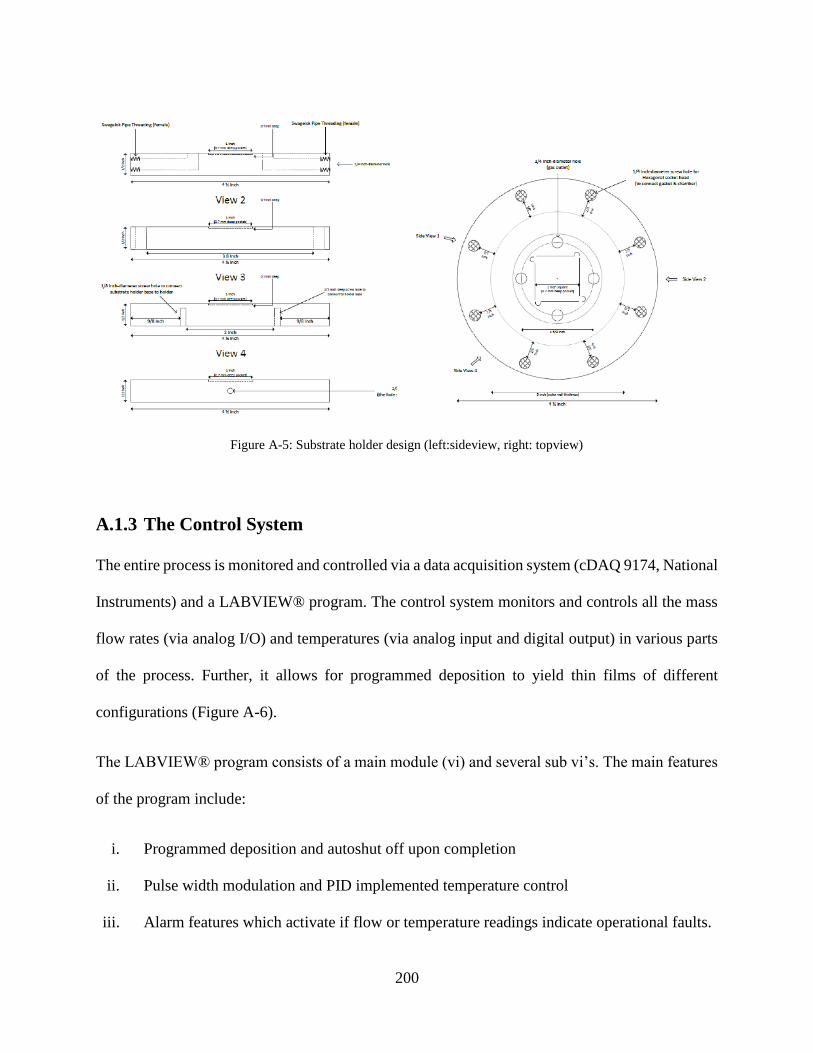
200
A.1.3 The Control System
The entire process is monitored and controlled via a data acquisition system (cDAQ 9174, National
Instruments) and a LABVIEW® program. The control system monitors and controls all the mass
flow rates (via analog I/O) and temperatures (via analog input and digital output) in various parts
of the process. Further, it allows for programmed deposition to yield thin films of different
configurations (Figure A-6).
The LABVIEW® program consists of a main module (vi) and several sub vi’s. The main features
of the program include:
i. Programmed deposition and autoshut off upon completion
ii. Pulse width modulation and PID implemented temperature control
iii. Alarm features which activate if flow or temperature readings indicate operational faults.
Figure A-5: Substrate holder design (left:sideview, right: topview)

201
iv. Safety auto shutdown if alarms remain active for more than 15 secs continuously. System
informs the operator automatically via text message.
Since the main vi block diagram is large, it has been shown in sections (Figure A-7 Section 1-7).
This is followed by the sub vi’s. Only one subvi of each type has been shown – Mass flow
controller sub vi and heater PID subvi.
Figure A-6: Possible film configurations which can be synthesized by the ACVD
system

202
Figure A-7: Overview of the Labview main vi.

203

204

205

206

207

208

209

210
Figure A-8: Block diagram of a mass flow controller sub vi.

211
Figure A-9: Block diagram of heater control sub vi implemented via pulse-width modulation and PID control

212
Figure A-10: Front Panel of the Labview program for the ACVD system

213
A.2 Standard Operating Procedure
Version 3.0 – Updated on 02/02/2016 by Tandeep S. Chadha
A.2.1 Scope and Applicability
This standard operating procedure applies to the operation of the multicomponent Aerosol
Chemical Vapor Deposition (ACVD) reactor in Room 3035. The ACVD reactor is used to
synthesize thin films of single component and mixed metal oxides (TiO2, Nb doped TiO2, SnO2)
with well controlled morphologies for several applications.
A.2.2 Summary of the Method
An ACVD reactor is used to synthesize thin films of metal oxides with smooth, granular or
columnar morphologies on different substrates (Stainless steel, ITO coated glass, FTO coated
glass) for various applications. The process parameters in the reactor determine the morphology
of the thin film formed.
A.2.3 Definitions
ACVD: Aerosol Chemical Vapor Deposition.
TTIP: Titatnium(IV) Isopropoxide
TMT: Tetramethyl Tin
Nb ethoxide: Niobium (V) ethoxide
NTO: Niobium doped TiO2
PPE: Personal protective equipment

214
EHS: Environmental Health and Safety Office
A.2.4 Health and Safety Warnings
i. The ACVD operates at high temperatures (up to 600 C). Extreme care and caution should
be taken to prevent injury from burns. Flame retardant PPE should be used when operating
the ACVD. Make sure that non approved personnel in the lab area are fully aware of the
risks during ACVD operation.
ii. The ACVD generates aerosol nanoparticles. The ACVD enclosure should always be vented
in a fume hood. Extreme care should be taken to prevent any leakages of nanoparticles in
the lab environment. Risks for nanoparticle inhalation should be minimized.
A.2.5 Equipment and Supplies
i. Personal Protective equipment:
a. Safety glasses (worn at all times)
b. Nitrile gloves (worn at all times)
c. Flame retardant lab coat (worn at all time)
d. Heat protective glove (worn while sample exchange)
e. N95 particulate mask (worn while FLAR is in operation
ii. Chemicals and gases (see appendix for MSDS)
a. Titanium(IV) Isopropoxide
b. Niobium Ethoxide
c. Tetramethyl Tin
d. Pressurized gas (Oxygen, Nitrogen, Hydrogen)

215
A.2.6 Apparatus and Materials
i. Enclosure hood-used to contain the generated aerosols, must be kept under negative
pressure at all times
ii. ACVD deposition substrate with glass cover. The deposition substrate is maintained at high
temperature. Caution must be taken while handling the substrate or the glass cover.
iii. Mass flow controllers-used to control gas flow rates in the ACVD. All gas lines supplying
MFCs should be maintained below 40 psi line pressure.
iv. Precursor bubblers (X2)-used to contain the precursors for nanoparticle generation. These
precursors are typically metal organic compounds and can be toxic when inhaled thus they
must always be properly sealed. If the bubblers leak/break, spray water onto/near the
bubblers to hydrolyze the precursors so they form inert oxides. If toxic substance, contact
EHS.
v. Precursor feeder tube attached to the delivery line. This tube can get hot during operation.
Heat protective gloves must be worn while handling.

216
Figure A-11: Photograph of the ACVD process reactor

A.2.7 Procedures
A.2.7.1 Preliminary Checklist
□ Make sure all proper PPE is being worn
□ Fittings are all properly tightened
□ Gas tanks are adequately full while the regulators are at the right pressure
□ Flow valves are operating normally and in the right position
□ Mass flow controllers are warmed up and stable
□ Check the flow rates of the gas in the mass flow controllers using the Gilibrator (if
necessary)
□ No leakages are detected
□ The precursor bubblers are properly filled
□ Precursor delivery lines are properly wrapped
A.2.7.2 System Startup
1. Ensure that the water/oil level in the isothermal water/oil bath around the precursors is full.
Fill additional water/oil if required.
2. Turn on all power switches attached to the system.
3. Turn on the MFC power box.
4. Turn on the PC and RUN the labview program.
5. In the program front panel, switch on the needed heaters and set the desired substrate
temperature, delivery tube temperatures and precursor temperatures. Allow temperature to
stabilize. This will take usually 1 hour.
6. Clean the feeder tube and the glass cover and place in the oven to dry.

218
A.2.7.3 System Stabilization
7. Place the glass cover on the substrate holder.
8. Attach the precursor tubing to the system. Use 2 wrenches to tighten and ensure that
precursor feed lines are not disturbed.
9. Raise the level plate upto the standard plate level. Check height using level indicator.
10. Take a glass slide. Cut using a diamond scribe.
11. Place the glass slide onto the substrate using tweezers.
12. Open the central nitrogen supply valve (on the fume hood).
13. In the program, select which precursors will be used and set the desired precursor and
dilution flow rates in the labview program.
14. Set the deposition time to 180 mins and turn on the deposition switch on the program.
15. After 180 mins the deposition switch will automatically turn off.
16. Lift the glass cover and take out the slide
A.2.7.4 Depositing on desired substrates
17. Lower the level plates.
18. Remove the precursor feeding nozzle. Use two wrenches.
19. With heat resistant gloves on, clean the nozzle with tissue and ethanol. Then blow air into
the nozzle to ensure complete drying.
20. Tighten to the setup again as descried in step 8.
21. Keep the substrate on the substrate holder using tweezers. Ensure that the substrate covers
the entire substrate pocket on the holder. If not, place a steel foil below the substrate.
22. If needed, place a mask on one side of the slide to ensure deposition free area for attaching
the electrode.

219
23. In the program, select which precursors will be used and set the desired precursor and
dilution flow rates in the labview program.
24. Set the desired deposition time and turn on the deposition switch on the program.
25. After the set deposition time is over, the deposition switch will automatically turn off.
26. Lift the glass cover and take out the substrate.
27. Hold the substrate using tweezers in air and shake to cool. DO NOT place directly on table
if glass.
28. After the susbtrate has cooled down, place it on the table.
29. Repeat steps 17-28 for subsequent samples.
A.2.7.5 Switching off the system
30. Turn off al heaters in the program.
31. Switch the three way valves on the precursors to purge mode (bypassing the bubbler)
32. Repeat steps 17-28 with a glass sample, 15 mins deposition time with a flow rate of atleast
500 ccm through all precursors.
33. Turn off the labview program by hitting the big STOP button. DO NOT switch off the
program from the labview software terminated button on the top.
34. Turn of all gass supply valves in the system.
35. Lower the level plates and remove the feeder tube.
36. Remove the glass cover and place upside down (Narrow portion down) on the side.
37. Turn off mass flow controller power box and PC.
38. Switch off all power switches.

220
Appendix B
COMSOL model setup for simulating fluid
dynamics and heat transfer in the ACVD
Reactor

221
B.1 Global Definitions
B.1.1 Parameters
Name Expression Description
T_s0 723.15 Substrate temperature
Q_in0 9.17E-6 Inflow rate
E 74.03e3[J/mol] Activation Energy
A 1.54e6[1/s] Frequency factor
T_in0 323.15 Inflow temperature
h0 20[mm] tube height from substrate
ts 2[mm] substrate thickness
Rs 37.5[mm] Radius of substrate
tc 3[mm] Thickness of the cover
h1 90[mm] first height of the cover stair
h2 110[mm] total height from the substrate
Rt 4[mm] tube inner radius
tt 1[mm] tube thickness
w 19[mm] cover radius change
Rs2 10[mm] Radius of the substrate 2
ts2 1[mm] thickness of the substrate 2
c0 0.0060 Initial concentration of TTIP

222
B.2 Model 1 (mod1)
B.2.1 Geometry 1
B.2.1.1 Units
Length unit mm
Angular unit deg
B.2.1.2 Geometry statistics
Property Value
Space dimension 2
Number of domains 7
Number of boundaries 28
Figure B-1: Setup of the geometry of the ACVD reactor in COMSOL.

223
B.3 Materials
B.3.1 Air
B.3.1.1 Selection
Geometric entity level Domain
Selection Domains 3–4, 6
Figure B-2: Setup of simulation domains in COMSOL. The domain highlighted
in blue is air.

224
B.3.2 Steel AISI 4340
B.3.2.1 Selection
Geometric entity level Domain
Selection Domains 1, 5
Figure B-3: Setup of simulation domains in COMSOL. The domains
highlighted in blue are steel.

225
B.3.3 Silica glass
B.3.3.1 Selection
Geometric entity level Domain
Selection Domains 2, 7
Figure B-4: Setup of simulation domains in COMSOL. The domain highlighted
in blue is silica glass.

226
B.4 Heat Transfer (ht)
Features
Heat Transfer in Fluids 2
Axial Symmetry 1
Thermal Insulation 1
Initial Values 1
Heat Transfer in Solids 2
Temperature 1
Convective Cooling 1
Open Boundary 1
Outflow 1
Figure B-5: Setup of the heat transfer module for the ACVD reactor. Domains
for which the heat transfer simulation was carried out are highlighted in blue.

227
B.5 Laminar Flow (spf)
Features
Fluid Properties 1
Axial Symmetry 1
Wall 1
Initial Values 1
Inlet 1
Wall 2
Outlet 1
Figure B-6: Setup of the heat transfer module for the ACVD reactor. Domains
for which the laminar flow simulation was carried out are highlighted in blue.

228
B.6 Transport of Diluted Species (chds)
Features
Convection and Diffusion 1
Axial Symmetry 1
No Flux 1
Initial Values 1
Inflow 1
Outflow 1
Figure B-7: Setup of the transport of diluted species module for the
ACVD reactor. Domains for which the transport of diluted species
simulation was carried out are highlighted in blue.

229
B.7 Mesh 1
B.8 Study1
B.8.1 Stationary
Mesh selection
Geometry Mesh
Geometry 1 (geom1) mesh1
Physics selection
Physics Discretization
Heat Transfer (ht) physics
Laminar Flow (spf) physics
Transport of Diluted Species (chds) physics
Figure B-8: Mesh formulation for the ACVD reactor simulation in COMSOL

230
Curriculum Vitae
Tandeep S. Chadha Email: [email protected]
ACADEMIC BACKGROUND
2016 Ph.D., Energy, Environment and Chemical Engineering., Washington University
in St. Louis.
Advisor: Prof. Pratim Biswas
2013 M.S., Energy, Environment and Chemical Engineering., Washington University
in St. Louis
2009 B.Tech., Biotechnology, SASTRA University, Thanjavur, India
PROFESSIONAL EXPERIENCE
2014-
present
Co-Founder, Applied Particle Technology, LLC
Developing and commercializing a disruptive air–purification technology
Principal Investigator for a National Science Foundation STTR Phase I grant
“Soft X-ray Enhanced Electrostatic Precipitator for High Efficiency Air
Purification in Indoor Environments” (Jan–Dec 2016)
RESEARCH EXPERIENCE
2010-
present
Graduate research assistant, Washington University in St. Louis
Ph.D. Thesis: “Synthesis of nanostructured thin films by chemical vapor-aerosol
deposition (CVAD) process for energy applications.”
2009-2010 Junior research fellow, IIT Bombay, Mumbai, India
Aerosol routes for the synthesis of nanoparticles with controlled structural
properties” Applications to biodegradable particles for drug delivery
2008 Summer research intern, Chung-Ang University, Seoul, South Korea
2D patterning of gold nanoparticles on PS-b-PEO block copolymer thin
films
and crystallization of Guanosine-5’-Monophosphate to identify new
crystal polymorphs
2007-2008 Undergraduate research, SASTRA University, Thanjavur, India
Synthesis of anti-microbial properties of silver nanoparticles for applications in
water purification.
HONORS AND AWARDS
2015 Global Impact Award 2015, Washington University in St. Louis
2015 Breakthrough Technology of the Year Award 2015, CleanTech Open

231
2015 Winner, Arch Grants for the development of Applied Particle Technology
2015 Student Travel Award, Battery Division, 227th Meeting of the Electrochemical
Society, Chicago, IL
2014 Student Travel Award, Battery Division, 226th Meeting of the Electrochemical
Society, Cancun, Mexico
2014 Graduate Student Teaching Assistant Award, Department of Energy
Environmental and Chemical Engineering, Washington University in St. Louis
2013 Best poster award, 32nd American Association for Aerosol Research Annual
Conference, Portland, OR
2012 Student Travel Award, 31st American Association for Aerosol Research Annual
Conference, Minneapolis, MN
2011 Best poster award, 30th American Association for Aerosol Research Annual
Conference, Orlando, FL
2010-2011 Recipient of Cheryll Walzel-Frick & F. Alan Frick Endowed Scholarship
PROFESSIONAL ACTIVITIES
2012-2014 Student co-ordinator for McDonnell Academy Global Energy and Environment
Partnership (MAGEEP). Initiated the development of a global education network
platform for course development and delivery.
2010-2011 Elected Vice-President of Umang - Indian Graduate Students Association,
Washington University in St. Louis
PATENTS, PUBLICATIONS AND PRESENTATIONS
Patents:
1. Chadha, T.S., Biswas, P, An, W-J., (2014) “Single-Step Synthesis of
Nanostructured Thin Films by a Chemical Vapor Aerosol Deposition Process”,
US2016/0056448
2. Biswas, P., Chadha, T.S., Fang, J., “Systems and Methods for Gas Cleaning Using
Electrostatic Precipitation and Photoionization”, Provisional Application Filed.
Journal Publications:
1. Kavadiya, S., Chadha, T. S., Liu, H., Shah, V. B., Blankenship, R. E., & Biswas, P.
(2016). Directed assembly of the thylakoid membrane on nanostructured TiO 2 for
a photo-electrochemical cell. Nanoscale, 8(4), 1868-1872.
2. Raliya, R., Chadha, T. S., Haddad, K., & Biswas, P. (2016). Perspective on
nanoparticle technology for biomedical use. Current Pharmaceutical Design,
22(17), 2481-2490.
3. Vazquez-Pufleau, M., Chadha, T.S., Yablonsky, G., Erk, H., Biswas, P., (2015)
“Elimination of Carbon Contamination from Silicon Kerf using a Furnace Aerosol
Reactor (FuAR) Methodology”, Industrial and Engineering Chemistry Research,
54(22), 5914-5920.
4. Shah, V.B., Henson, W., Chadha, T.S., Lakin, G., Liu, H., Blankenship, R., Biswas,
P. (2015) “Linker-Free Deposition and adhesion of Photosystem I onto
Nanostructured TiO2 for Biohybrid Photo-electrochemical Cells”, Langmuir, 31(5),
1675-1682.

232
5. Chadha, T.S., Tripathi, A.M., Mitra, S., Biswas, P. (2014). “One-Dimensional,
Additive-Free, Single Crystal TiO2 Nanostructured Anodes Synthesized by a Single
Step Aerosol Process for High Rate Lithium-Ion Batteries”, Energy Technology
2(11), 906-911. (Journal inside cover highlight article)
6. Chadha, T.S., Park, J., An, W.J., Biswas, P. (2014) “Gold Nanocage Coupled Single
Crystal TiO2 Nanostructures for Near-Infrared Water Photolysis”, Journal of
Nanoparticle research, 16(11), 1-9.
7. Fang, J., Wang, Y., Attoui, M., Chadha, T.S., Ray, J.R., Wang, W.N., Jun, Y.S.,
Biswas, P., (2014) “Measurement of Sub-2 nm Clusters of Pristine and Composite
Metal Oxides during Nanomaterial Synthesis in Flame Aerosol Reactors”,
Analytical Chemistry, 86(15), 7523-7529.
8. Park, J., Ozdemir, S.K., Monifi, F., Chadha, T.S., He, S.H., Biswas, P., Yang, L.
(2014). “On-Chip Titanium Dioxide Whispering Gallery Microcavities”, Advanced
Optical Materials, 2(8), 711-717.
9. Wang Y., Fang, J., Attoui, M., Chadha, T.S., Wang, W.N., Biswas, P. (2014).
“Application of Half Mini DMA for sub 2 nm Particle Size Distribution
Measurement in Electrospray and a Flame Aerosol Reactor” Journal of Aerosol
Science, 71, 52-64.
10. Henson, W.R., Shah, V.B., Lakin, G., Chadha, T.S., Liu, H., Blankenship, R.E.,
Biswas, P. (2013). “Production and Performance of a Photosystem I Based Solar
Cell Using Nano-Columnar TiO2”, Proceedings of the 39th IEEE Photovoltaics
Specialists Conference, Tampa, FL, 2705-2709, 2013.
11. Chadha, T. S., Chattopadhyay, S., Venkataraman, C., & Biswas, P. (2012). “Study
of the charge distribution on liposome particles aerosolized by air-jet
atomization” Journal of Aerosol Medicine and Pulmonary Drug Delivery, 25(6),
355-364.
12. Chadha, T.S., Yang, M.M., Haddad, K., Shah, V., Li, S., & Biswas, P., “Multi-scale
Model to Predict Nanostructured Thin Film Morphology in an Aerosol Chemical
Vapor Deposition Process”, submitted to Chemical Engineering Journal, July
2016.
13. Chadha, T.S., Suthar, B., Rife, D., Subramanian, V., & Biswas, P., “Model based
analysis of one-dimensional oriented lithium ion battery electrodes”, submitted to
Journal of Power Sources, July 2016.
14. Chadha, T.S., Dutta, P., Raliya, R., Mitra, S., & Biswas, P., “Additive-free Anatase
Dendrites as Ultra-stable Anodes for Sodium-ion Batteries”, submitted to Journal
of American Chemical Society, July 2016.
15. Raliya, R., Saha, D., Chadha, T.S., Raman, B., & Biswas, P, “Aerosol based gold
nanoparticles delivery to brain: A non-invasive approach to cross the blood-brain
barrier”, submitted to Nanoscale, July 2016
16. Jung, H., Chadha, T.S., Kim, D., Biswas, P., & Jun, Y-S, “Photochemically-assisted
Fast Oxidation of Manganese and Formation of δ-MnO2 Nanosheets”, submitted to
Nature Geoscience, July 2016
17. Haddad, K., Kavadiya, S., Chadha, T.S., Wang, Y., Raliya, R., & Biswas, P.,
“Growth of oriented, single crystal SnO2 Nanocolumn Arrays by Aerosol Chemical
Vapor Deposition (ACVD)”, submitted to CrystEngComm, June 2016.

233
18. Vazquez-Pufleau, M., Chadha, T.S., Yablonsky, G., & Biswas, P., “Determination
of activation energy of carbon elimination from Si kerf by thermogravimetric
analysis and insights in its reaction mechanism” in preparation
19. Fang, J., Guo, Z., Raliya, R., Chadha, T.S., Banerjee, P., & Biswas, P.,
“Combustion synthesis of niobium doped TiO2 thin nanostructured thin films”, in
preparation
20. Chadha, T.S., Dutta, P., Raliya, R., Fang, J., Mitra, S., & Biswas, P., “Single Step
Synthesis of Nb doped TiO2 nanostructured electrodes as high capacity anodes for
sodium ion batteries”, in preparation.
Selected Conference Presentations
1. Chadha, T.S., Haddad, K., Raliya, R., & Biswas, P. (2015). “Single step synthesis
of tin oxide nanopillar arrays by aerosol chemical vapor deposition (ACVD)” 34th
American Association for Aerosol Research Annual Conference, Minneapolis, MN.
2. Chadha, T.S., Shetty, P., Tripathi, A.M., Mitra, S., Biswas, P. (2015). “Gas Phase
Synthesis of One-Dimensional Single Crystal Tin Oxide Nanostructured Lithium-
Ion Battery Anodes”, 227th Meeting of the Electrochemical Society, Chicago, IL.
3. Rife, D., Chadha, T.S., Suthar B., Mitra, S., Subramanian, V., Biswas, P. (2015)
“Two-Dimensional Modeling of Columnar TiO2 Nanostructured Electrodes”, 227th
Meeting of the Electrochemical Society, Chicago, IL.
4. Shetty, P., Chadha, T.S., Biswas, P., Mukhopadhyay, A., Ramadesigan, V., (2015)
“Modeling the Effects of Morphology in Lithium-Ion Battery Electrodes”, 227th
Meeting of the Electrochemical Society, Chicago, IL.
5. Chadha, T.S., Rife, D., Tripathi, A.M., Mitra, S., Subramanian, V., Biswas, P.
(2014). “Understanding the Relationship of Nanostructure to Performance in
Additive Free TiO2 Anodes for Lithium-Ion Batteries”, 226th Meeting of the
Electrochemical Society, Cancun, Mexico.
6. Chadha, T.S., Fang, J., Biswas, P. (2014). “Single Step Aerosol Route Synthesis of
Mixed Oxide Nanostructures for Use as Additive Free Lithium Ion Battery
Electrodes”, 226th Meeting of the Electrochemical Society, Cancun, Mexico.
7. Fang, J., Chadha, T.S., Banerjee, P., Biswas, P. (2014). “Flame aerosol synthesis
of niobium-doped TiO2 nanostructured thin films for transparent conducting
oxides”, 2014 MRS Fall Meeting, Boston, MA.
8. Chadha, T.S., Tripathi, A.M., Mitra, S., Biswas, P. (2014). “Relationship of
Nanostructure to Performance of Single Step Aerosol Route Synthesized Carbon
Free TiO2 Anodes for Lithium-ion Batteries”, 2014 MRS Spring Meeting, San
Francisco, CA.
9. Wang Y., Liu, P., Chadha, T.S., Fang J., Biswas, P. (2014). “Kinetics of Sub 3 nm
Titanium Dioxide Particle Formation in an Aerosol Reactor during the Thermal
Decomposition of Titanium Isopropoxide (TTIP)”, 32nd American Association for
Aerosol Research Annual Conference, Portland, OR.
10. Chadha, T.S., Fang, J., Biswas, P. (2013). “Controlling Composition and
Morphology of Mixed Oxide Thin Films by Aerosol Chemical Vapor Deposition
Process”, 32nd American Association for Aerosol Research Annual Conference,
Portland, OR.

234
11. Chadha, T.S., Yang, M., Li, S., Biswas, P. (2013). “TiO2 Nanoparticle Formation
and Growth in Aerosol Chemical Vapor Deposition (ACVD) Systems: Discrete
Sectional Simulation”, 32nd American Association for Aerosol Research Annual
Conference, Portland, OR.
12. Wang Y., Fang, J., Chadha, T.S., Wang, W.N., Biswas, P. (2013). “Comparison of
Half Mini DMA and Nano DMA for Measurement of Size Distributions in
Electrospray and a Flame Aerosol Reactor”, 32nd American Association for Aerosol
Research Annual Conference, Portland, OR..
13. Biswas, P., Chadha, T.S., Shah, V.B., Henson, W.R. (2013). “Aerosol Nanoparticle
Technology Enabling Solar Research and Development”, Indo-US workshop on
nano-structured electronic materials, Thrissur, India (Invited Talk).
14. Chadha, T.S., Park, J., An, W.J., Biswas, P. (2012). “Effect of Shape and Size of
Au Nanoparticles on the Water-Splitting Performance of Au-TiO2 Thin Films”, 31st
American Association for Aerosol Research Annual Conference, Minneapolis, MN
15. Chadha, T. S., Chattopadhyay, S., Venkataraman, C., & Biswas, P. (2011). “Study
of the charge distribution on aerosolized liposomes generated by air jet
atomization”, 30th American Association for Aerosol Research Annual Conference,
Orlando, Fl
16. Pawar, A.A., Chadha, T.S., Venkataraman, C., Mehra A. (2010). “Synthesis of
Solid Nanoparticles with Hydrophillic Cores in a Low Temperature Aerosol
Reactor (LoTAR)” Conference of Indian Aerosol Science and Technology (IASTA),
Darjeeling, India
17. Vidya, M., Chadha, T.S., Maheswari, K.U. (2007). “A Novel Enzyme Assay for
the enzyme Thiopurine Methyltransferase to identify the variants of the TPMT
gene” Indo-Australian Conference on Human Variations and Pharmacogenomics,
Manipal, India