Structure-dependent optical and electrical transport properties of nanostructured Al-doped ZnO

ISSN: 0975-8585
July - August 2014 RJPBCS 5(4) Page No. 615
Research Journal of Pharmaceutical, Biological and Chemical
Sciences
Sol-Gel Dip Coated Pure and Fe-Doped Nanostructured ZnO Thin Films.
Brahmaiah Vutukuri, Vignesh Elavalagan, Ganesh Kumar Mani, Prabakaran Shankar and John Bosco Balaguru Rayappan*
Centre for Nanotechnology & Advanced Biomaterials (CeNTAB) and School of Electrical & Electronics Engineering (SEEE) SASTRA University, Thanjavur 613 401, Tamil Nadu, India
ABSTRACT
Pure and Fe-doped zinc oxide thin films were coated on glass substrates using sol-gel dip technique. Zinc
acetate dihydrate and ferrous chloride anhydrous were used as the host and dopant precursor salts respectively. X-ray diffraction patterns confirmed the hexagonal wurtzite structurewith polycrystalline nature of the films. Morphological studies revealed the tightly packed spherical shaped grains for both the pure and Fe-doped films. The optical characteristics were observed using UV- Vis spectrophotometer in the wave length range of 300-800 nm. The Fe-doped ZnO film showed a greater absorption in the visible region compared to that of pure ZnO film. The decrease in band gap and electrical resistance with Fe-doping were observed for the Fe-doped ZnO thin film. Keywords: Sol-gel; ZnO; Doping; Thin films. *Corresponding author
ISSN: 0975-8585
July - August 2014 RJPBCS 5(4) Page No. 616
INTRODUCTION
One of the most prominent metal oxide materials namely zinc oxide (ZnO) has been exploited to the core by the scientific community due to its functional and catalytic nature. Being an n-type semiconducting material with larger band gap (3.37 eV) and exciton binding energy (∼60 meV)[1–3], itattracts scientists across various fundamental and applied fields of science due to its resourcefulness. It has been identified as one of the versatile and predominant candidates for the electronic, optoelectronic, sensing, solar cell and laser applications[4–6]. Moreover, the field of “nano” has surprisingly brought out the low dimensional features of this flexible material to a newer dimension. The different nanostructures of ZnO and their uniqueness indeed captured a reasonable map of the literature on the metal oxide materials. The presence of intrinsic defects like oxygen vacancies and zinc interstitialsin the ZnO nano scale has furthered its applications in the area of magnetic devices[7].
Structural, morphological, optical and electrical properties of thethin film form of this “Queen of Metal Oxides”can be varied by modulating the different synthesize parameters of both the physical and chemical deposition techniques. Further, tuning of its transport properties by impurity doping has reached newer heights in the recent past. Doping ZnO has helped to modulate the band gap and hence all its related electronic and optical properties in-turn resulted in the development of modern optoelectronic devices. In the past, metal oxides like TiO2[8], MoO3[9], CuO[10]were doped with ZnO but in recent times, doping transition metals (TM) like Mn, Fe, Ni and Co in ZnO has gained significanttechnological advantages in fabricating spintronic and optoelectronic devices[11–13].Among these transition metals, Fe doping in ZnO has strongly influenced the magnetic behavior of ZnO and particularly Fe-dopingfacilitates the manipulation ofits charge and spin degrees of freedom[11].In particular, the partially filled d states of Fe atom has a strong influence on exhibiting the magnetic behavior of ZnO. The electronic state interaction or exchange between Fe dopants and host ZnO, directly influence its band gap by raising and lowering the valence and conduction band edges respectively[14,15].Chenet al.reported the influence of Fe-dopants on the structural and photoluminescence characteristics of ZnO thin films[16]. Similarly,the effect of synthesize conditions and Fe-doping on the various characteristic features of ZnO thin films were investigated by Zhanget al.[12].
Since deposition parameters of various thin film coating techniqueslikespray pyrolysis, citrate decomposition, hydrothermal, RF sputtering, pulsed laser deposition, etc., play a crucial role in fine-tuning the physical and chemical properties of ZnO, sol-gel dip technique has been considered in this work to deposit Fe-doped ZnO thin film. Compared to other techniques sol-gel dip coating has many advantagessuch as simple deposition conditions, cost effectiveness and control over the structural and morphological properties of thin films [1,17].Hence in this work, a major focus is given to investigate the structural, morphological, optical, electrical properties of Fe-doped ZnO thin films employing sol-gel dip coating technique.

ISSN: 0975-8585
July - August 2014 RJPBCS 5(4) Page No. 617
MATERIALS AND METHODS Film deposition
Pure and Fe-doped nanostructured ZnO thin films were coated on glass substratesusingsol-gel dip coating (HOLMARC, HO-TH-02)technique. Zinc acetate dihydrate [Zn(CH3COO)2.2H2O, (Sigma Aldrich, 99% purity)] and ferrous chloride anhydrous [FeCl2, (MERCK, 99% purity)]were used as the precursor salts. Ethanol and monoethanol amine were used as solvent and stabilizer respectively.The sol was prepared by dissolving 0.05 M of zinc acetate dihydrate and ferrous chloride anhydrous in a mixture of 25 ml of ethanol and 0.05 M of MEA. The molar ratio of the dopant atoms in the precursor solution was considered as 0 and 2 at%. The solution was stirred at room temperature for 15 min to produce clear solution.Flow chart representing the deposition of undoped and Fe-doped ZnO films is shown in Fig.1. Glass substrates (Blue Star, Mumbai) were ultrasonically (Supersonic, Mumbai) cleaned with acetone and deionized water for 15 min. Films were coated by dipping them at the speed of 9000 μm/sec and retrieving them by 1000 μm/sec speed. The time of interval between each dipping and drying was maintained at 1 min in order to avoid “peeling off” as a layer and also to enhance the adhesive nature of the films. All the coating conditions were auto controlled by the processor.Films were deposited on glass substrates by preheating the substrate at 348 Kbefore each dipping cycle. The dip coating and preheating were repeated 5 times. The pure and Fe-doped ZnO films were subsequently annealed at 723 K for 3 hrs. Characterization techniques
Structural characteristics of the films were studied using X-ray diffractometer (X’PERT PANanalytical, Netherland) with Cu Kα source (λ =1.5408 Å) in the 2θ range of 10 to 80o. Surface morphology of the films was examined using Field Emission Scanning Electron Microscope (FE-SEM) (JSM-6701F, JEOL, Japan). Optical properties were studied using UV-Vis spectrophotometer (Perkin Elmer, Lambda 25, USA) in the wavelength range of 300 to 800 nm. The electrical conductivity was measured using two probe electrometer (6517A, Keithley Inc., USA).
RESULTS AND DISCUSSION Structural studies
The structural features of the undoped and Fe-doped ZnO thin films were characterized using X-ray diffractometer (Fig. 2). Both the pure and Fe-doped filmswere found to be polycrystalline in nature with hexagonal wurtzite structure. The diffraction peaks corresponding to (100) (002) (101) planes were observed. There was no specific diffraction patterns were observed for anysecondary phases such as FeO, Fe2O3,Fe3O4and Zn2Fe4O. Thishas confirmed that the Fe atoms were perfectly replacedthe Zn atoms. The crystallite size was calculated usingDebye Scherrer (Eq. 1) formula and was found to be 15 and 27 nm for the pure and Fe-doped films respectively.
ISSN: 0975-8585
July - August 2014 RJPBCS 5(4) Page No. 618
(1)
where, ‘D’ is the crystallite size, ‘λ’ is the wavelength of the X-ray used (1.5406 Å for Cu Kα), ‘θ’ is the Bragg’s angle and ‘β’ is the full width at half maximum. It can be seen from the XRD patterns that the FWHM washigh for undoped sample, whereas for Fe-doped ZnO film the FWHM was decreased. This decrease in FWHM confirmed the increase in crystallite size for Fe-doped ZnO film[18]. Morphological studies
Scanning electron micrographs of the pure and Fe-doped ZnO thin films are shown in Fig. 3, which showed the formation of films with a tightly packed spherical shaped grains.The surface morphology of pure filmshoweda uniform distribution of smaller grains throughout the substrate, whereas the micrograph of Fe-doped films showed an unevenly arranged larger grains with voids. This increase in grain size was also revealed by the XRD data. Optical studies
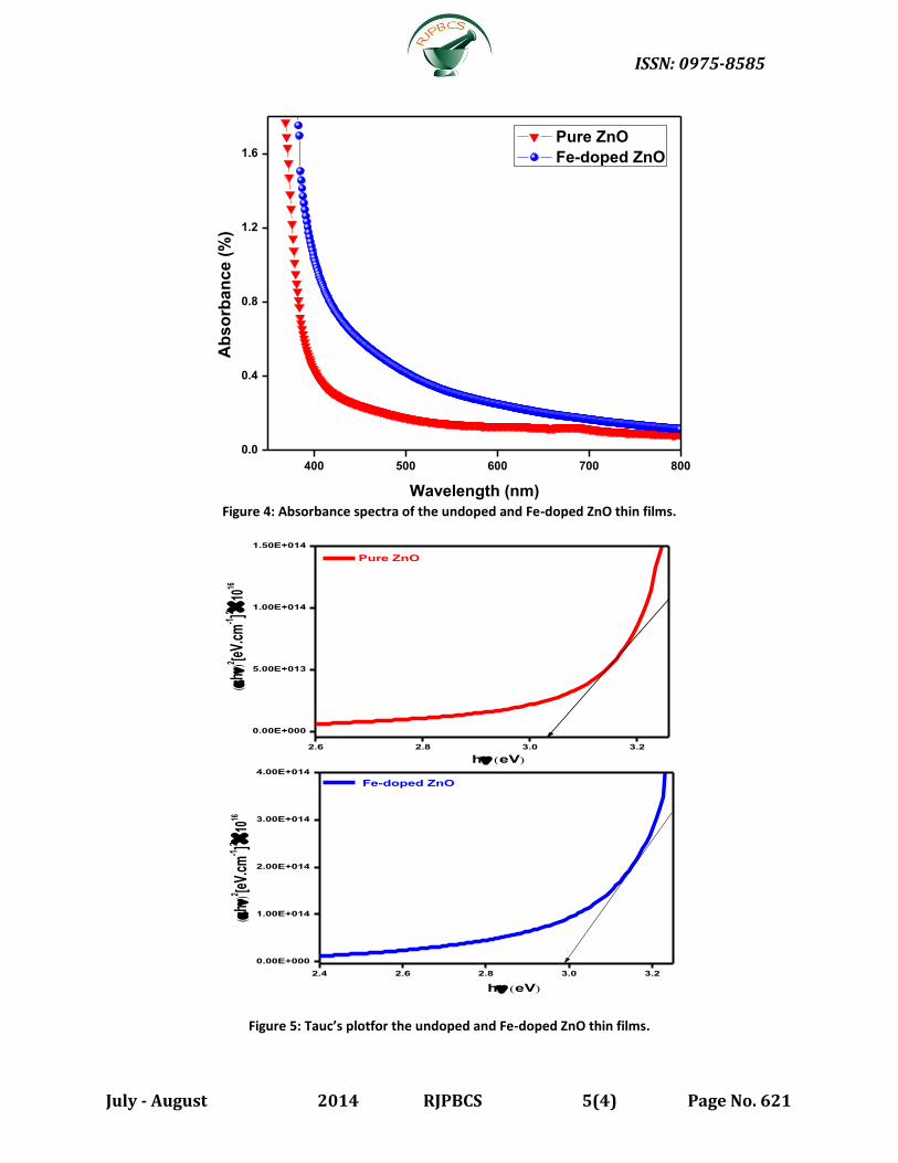
The optical absorbancespectra of theannealed pure and Fe-doped ZnO thin films are shown in Fig. 4. Fe-doped ZnO thin film showeda higherabsorption of photons in the visible region and low absorption in the region below 350 nm. This increase in absorption between 350-400 nm might be due to the radiative direct transition of electrons.A sharp absorption edge rise at 390 nm for the pure sample corresponds to the characteristic spectrum of pure ZnO. For Fe-doped sample the absorption region was found to be extended from UV to UV-Visible region. This has confirmed the incorporation of Fe-dopants into ZnO lattice as well as the formation of new donor impurity level below the conduction band of ZnO[19].Optical band gap values of the films werecalculated using Tauc’s plot by plotting (αhν)2 versus hν and extrapolating the linear portions of the absorption edge to find the intercept with energy axis. Fig. 5 shows the band gap variation of the pure and Fe-doped ZnO thin films. The band gap energy value was found to be decreased for the Fe-doped film. This decrease in band gap might be due to the sp-d spin exchange interaction betweenhost and dopant ions , which in-turn influenced the valence and conduction band edges resulted in a reduced band gap[14,15,20]. Electrical studies
The electrical conductivity behaviour of the pure and Fe-doped ZnO thin films aredepicted in Fig. 6. The electrical conductivity of Fe-doped ZnO thin film was found to be increased with reference to the pure film. This might be due to the increase in crystallite size and also increase in donor concentration of the Fe-doped ZnO thin film [17,21].

ISSN: 0975-8585
July - August 2014 RJPBCS 5(4) Page No. 619
CONCLUSION
Figure 1: Flow chart representation of the deposition process.
In this investigation, pure and Fe-doped ZnO thin films were successfully depositedon
glass substrates using sol-gel dip coating. The influence of Fe-doping on the structural, morphological, optical and electrical properties of ZnO were observed and correlated.The deposited films showed polycrystalline nature witha preferential orientation along (002) plane. Morphological studies revealedthe formation of films with tightly packed spherical shaped grain morphology. Optical studies revealed the enhanced absorption of photons by the Fe-doped ZnO thin film. The optical band gap energy and electrical resistanceof the ZnO film was found to be decreased upon Fe-doping.
Zinc Acetate dihydrate
(0.05 M) Zn (CH3COO)2.2H2O
(0.05 M) Zn(CH3CO2)2.2H2O
2 at% Ferrous Chloride
anhydrous (FeCl2)
Pre heated at 75 ˚C for each
dip
Dip coating
Clear solution
Stirred for 15 min
25 ml ethanol
Dried at room temperature
Annealed at 450˚C for
3 h
Fe-doped ZnO thin films
MEA
Dipping Speed–
9000 μm/s
Retrieval Speed –
1000 μm/s
Dipping Duration –
1 min
Drying Duration –
1 min

ISSN: 0975-8585
July - August 2014 RJPBCS 5(4) Page No. 620
30 40 50
Inte
ns
ity
(a
.u.)
Pure ZnO
Fe-doped ZnO
(10
0)
(10
1)
2deg.
(00
2)
Figure 2: X-raydiffraction patterns of the undoped and Fe-doped ZnO thin films.
Figure 3: FE- SEM images of the undoped and Fe-doped ZnO thin films.
Pure ZnO
Fe-doped ZnO
Pure ZnO
Fe-doped ZnO
ISSN: 0975-8585
July - August 2014 RJPBCS 5(4) Page No. 621
400 500 600 700 800
0.0
0.4
0.8
1.2
1.6
Ab
so
rba
nc
e (
%)
Wavelength (nm)
Pure ZnO
Fe-doped ZnO
Figure 4: Absorbance spectra of the undoped and Fe-doped ZnO thin films.
Figure 5: Tauc’s plotfor the undoped and Fe-doped ZnO thin films.
2.6 2.8 3.0 3.2
0.00E+000
5.00E+013
1.00E+014
1.50E+014
Pure ZnO
heV
h
2 [eV.
cm-1]2
1016
2.4 2.6 2.8 3.0 3.2
0.00E+000
1.00E+014
2.00E+014
3.00E+014
4.00E+014
Fe-doped ZnO
heV
h2 [e
V.cm
-1]2
1016
2.6 2.8 3.0 3.2
0.00E+000
5.00E+013
1.00E+014
1.50E+014
Pure ZnO
heV
h
2 [eV.
cm-1]2
1016
2.4 2.6 2.8 3.0 3.2
0.00E+000
1.00E+014
2.00E+014
3.00E+014
4.00E+014
Fe-doped ZnO
heV
h
2 [eV.
cm-1]2
1016

ISSN: 0975-8585
July - August 2014 RJPBCS 5(4) Page No. 622
Pure ZnO Fe-doped ZnO
5.0x10¹⁰
1.0x10¹¹
1.5x10¹¹
2.0x10¹¹
2.5x10¹¹
3.0x10¹¹
Ele
ctr
ica
l re
sis
tnc
e (
)
Figure 6: Electrical resistance variation of the undoped and Fe-doped ZnO thin films.
ACKNOWLEDGEMENTS
The authors wish to express their sincere thanks to the Department of science &
Technology, New Delhi, India for their financial support ( ID: INT/SWD/VINN/P-04/2011 and SR/FST/ETI-284/2011(C)). They also wish to acknowledge SASTRA University, Thanjavur for extending infrastructure support to carry out this work.
REFERENCES
[1] L Znaidi. Mater Sci Eng B 2010;174:18-30. [2] M Mirzaee, A Zendehnam, and S Miri. Sci Iran 2013;20:1071-1075. [3] J Lee, W Choi, C Kim, and J Hong. J Korean Phys Soc 2006;49: 1126-1129. [4] B Timmer, W Olthuis, and A Van Den Berg. Sens Actuators B Chem 2005; 107: 666-677. [5] V Kumar, RG Singh, F Singh, and LP Purohit. J Alloys Compd 2012;544: 120-124. [6] B Godbole. Mater Sci Appl 2011;02: 643-648. [7] XC Wang, WB Mi, and DF Kuang. Appl Surf Sci 2010; 256: 1930-1935. [8] S Siuleiman, N Kaneva, A Bojinova, K Papazova, A Apostolov, and D Dimitrov. Coll Surf A
Physicochem Eng Asp 2014; 1-6. [9] H.-L. Yu, et al. Sens Actuators B Chem 2012;679: 171-172. [10] DH Yoon, GM Choi. Sens Actuators B Chem 1999;55: 47-54. [11] A Goktas, IH Mutlu, and Y Yamada. Superlattices Microstruct 2013; 57: 139-149. [12] W.-G. Zhang, et al. Thin Solid Films 2011;519: 6624-6628. [13] A Srivastava, N Kumar, and S Khare. Opto-Electronics Rev 2014;22: 68-76.

ISSN: 0975-8585
July - August 2014 RJPBCS 5(4) Page No. 623
[14] KJ Kim and YR Park. J Appl Phys 2004;96: 4150-4153. [15] AP Rambu, V Nica, and M Dobromir. Superlattices Microstruct 2013;59: 87-95. [16] A Chen, X Wu, and Z Sha. J Phys D 2006;39: 4762-4765. [17] T Demet, T Guven, and B Duzgun. Rom J Phys 2013;58: 143-158. [18] AR Bushroa, RG Rahbari, HH Masjuki, and MR Muhamad. Vacuum 2012; 86: 1107-1112. [19] L Han, D Wang, Y Lu, T Jiang, L Chen, T Xie, and Y Lin. Sens Actuators B Chem 2013;177:
34-40. [20] DP Joseph and C Venkateswaran. J At Mol Opt Phys 2011; 2011: 1-7. [21] K Pandiadurai, GK Mani, P Shankar, and JBB Rayappan. Superlattices Microstruct 2013;
62: 39-46.
Copyright © 2022 FDOKUMEN