
Nanostructured Heterojunction Crystalline Silicon Solar Cells ...
219
General rights Copyright and moral rights for the publications made accessible in the public portal are retained by the authors and/or other copyright owners and it is a condition of accessing publications that users recognise and abide by the legal requirements associated with these rights. • Users may download and print one copy of any publication from the public portal for the purpose of private study or research. • You may not further distribute the material or use it for any profit-making activity or commercial gain • You may freely distribute the URL identifying the publication in the public portal If you believe that this document breaches copyright please contact us providing details, and we will remove access to the work immediately and investigate your claim. Downloaded from orbit.dtu.dk on: Aug 03, 2018 Nanostructured Heterojunction Crystalline Silicon Solar Cells with Transition Metal Oxide Carrier Selective Contacts Plakhotnyuk, Maksym Publication date: 2018 Document Version Publisher's PDF, also known as Version of record Link back to DTU Orbit Citation (APA): Plakhotnyuk, M. (2018). Nanostructured Heterojunction Crystalline Silicon Solar Cells with Transition Metal Oxide Carrier Selective Contacts. DTU Nanotech.
-
Upload
khangminh22 -
Category
Documents
-
view
0 -
download
0
Transcript of Nanostructured Heterojunction Crystalline Silicon Solar Cells ...

General rights Copyright and moral rights for the publications made accessible in the public portal are retained by the authors and/or other copyright owners and it is a condition of accessing publications that users recognise and abide by the legal requirements associated with these rights.
• Users may download and print one copy of any publication from the public portal for the purpose of private study or research. • You may not further distribute the material or use it for any profit-making activity or commercial gain • You may freely distribute the URL identifying the publication in the public portal
If you believe that this document breaches copyright please contact us providing details, and we will remove access to the work immediately and investigate your claim.
Downloaded from orbit.dtu.dk on: Aug 03, 2018
Nanostructured Heterojunction Crystalline Silicon Solar Cells with Transition MetalOxide Carrier Selective Contacts
Plakhotnyuk, Maksym
Publication date:2018
Document VersionPublisher's PDF, also known as Version of record
Link back to DTU Orbit
Citation (APA):Plakhotnyuk, M. (2018). Nanostructured Heterojunction Crystalline Silicon Solar Cells with Transition MetalOxide Carrier Selective Contacts. DTU Nanotech.

Nanostructured Heterojunction Crystalline Silicon Solar Cells with Transition Metal Oxide Carrier Selective Contacts
Maksym M. PlakhotnyukPhD Thesis May 2018


Nanostructured Heterojunction CrystallineSilicon Solar Cells with Transition Metal
Oxide Carrier Selective Contacts
Maksym M. PLAKHOTNYUK
THESIS FOR DOCTOR OF PHILOSOPHY DEGREE
Supervisor:Prof. Ole Hansen
Dr. Michael Stenbæk SchmidtDr. Tim Booth
May 14, 2018

ii
The title of the Ph.D. thesis:
Nanostructured Heterojunction Crystalline Silicon Solar Cells with Transition MetalOxide Carrier Selective Contacts
Author’s Name: Maksym M. PLAKHOTNYUK
Research Project Duration: August 2014 - March 2017
Supervisors:Prof. Ole Hansen, DTU NanotechDr. Michael Stenbæk Schmidt, DTU NanotechDr. Tim Booth, DTU Nanotech
Examiners:Dr. Anders Michael Jørgensen, Deputy Director of DTU Danchip,DenmarkAssistant Prof. Olindo Isabella, Delft University of Technology,NetherlandsAssociate Prof. Morten Madsen, Syddansk Universitet, Denmark
In collaboration with:

iii
PrefaceThis document concludes my last three years as a Ph.D. student at the Silicon Microtechnol-ogy group, Department of Micro- and Nanotechnology (Nanotech), Technical University ofDenmark (DTU). It also summarizes more than three years of intensive learning, laboratorywork, and personal search, challenging trails, falls, and rises. This work was funded by DTUinternal fund as a proof of concept Ph.D. project. The scope of the project has been to explorenew conceptual transition metal oxide carrier selective contacts in high-efficiency crystallinesilicon solar cells with improved light trapping black silicon nanostructures and graphenetop contact. After many experiments, tests, discussions I soon realized that it was a veryambitious plan considering the projects goals and realization period, available equipmentat the time. Nevertheless, I think I ended up with very interesting results and promisingnew concepts.
Fortunately for me, I was responsible for carrying all the process development, device fab-rication, and characterization. It gave me a chance to choose the interesting direction in myresearch, explore new ideas, and find collaborators in different parts of the world as well aswithin DTU and deliver this work to you.
Shortly, this work is about testing new concepts in the fabrication of crystalline silicon solarcell that could lead to a much cheaper solar cell with low toxic materials and with the sim-plified process flow. One of the concepts, transition metal oxide carrier selective contacts,such as TiO2 and NiO films, deposited by atomic layer deposition technique and RF sput-tering, will be discussed in Chapter 3 and 5. In Chapter 4, I will present the results on highlyefficient light trapping nanostructures, so-called black silicon. All the tested processes wereapplied in the fabrication of heterojunction silicon solar cells and these results are brieflypresented in Chapter 5. Even though most process development had remarkable results,the final fabricated solar cells displayed some severe defects that requires further analysisand device optimization.
Many of these results were possible to achieve only with support of other experts and friendsfrom the DTU Nanotech, Danchip, Energy and Physics, bachelor and master students, exter-nal collaborators from the University of Oslo, Martin Luther University Halle-Wittenberg,Fraunhofer CSP, SASTRA University, University of New South Wales and Freiberg Instru-ments Inc. Since the goal of this Ph.D. thesis is to show what my contribution has been, Iwill underline my personal input and contributions from others.
While on this project, I attended the QUANTSOL Ph.D. summer school on photovoltaics inAustria. The results of this thesis were presented as an oral and visual presentation at theinternational conferences on nanotechnology and photovoltaics in Stockholm, Singapore,Munich (EAMC, PVSEC-26, EU PVSEC-32, respectively). Two applications for patents werefiled with the design of high-efficiency silicon solar cells with metal oxides carrier selectivecontacts. Two articles were submitted for publications and two other articles are underpreparation. Hence, the knowledge attained while working on this project is transferred toother researchers in the Silicon Microtechnology group for use in recent and future projectson solar cells.
Finally, I would like to express my best gratitude to my family and friends who believed inme and provided support all the time.

iv
“If You Want To Go Fast, Go Alone. If You Want To Go Far, Go Together.”
Chinese proverb

v
To my beloved wife Lesia, son Maksym Junior and daughter Anna -for their support, patience, and belief in me during this time. . .
To my parents who will never see this work, but have always beenproud of. . .


vii
AbstractOne of the most severe challenges man is facing today is to satisfy the need for energywithout harmful environmental consequences. This complicated, grand challenge must bemet by a wide range of solutions; among these are more efficient use of resources and re-placement of fossil fuels by renewable energy sources. Any sustainable, renewable energysystem must directly or indirectly rely on solar energy. Photovoltaic or solar cells are al-ready efficient and reliable sources of electricity from solar light, but even though their costhas decreased significantly in recent years, solar cells are still far too costly for a competitiveproduction of bulk grid power. The challenge within the solar cell field is thus to reduce thecosts involved in solar cell production without sacrificing efficiency and reliability; actually,the efficiency should better improve towards 25 % or more, since the cell efficiency stronglyaffects the overall economy of a solar cell power plant. Currently, most of the solar cell mar-ket is based on 180-300 micrometer thick crystalline silicon wafers, and approximately 50% of the cost is due to the cost of the material. To reduce material costs, introducing thin-film cells is a promising alternative, but a limitation in thin film solar cell technologies isthat the absorptivity of light is quite weak, in particular for indirect band gap materials likesilicon. This limitation may be lifted by application of photon trapping strategies that canincrease the absorptivity of thin photo-absorbers by orders of magnitude at longer wave-lengths. Another proven approach in solar cell optimization is carrier selective contacts,such as conventional amorphous silicon, or wide bandgap metal oxide semiconductor.
In this Ph.D. thesis, I present several new ideas for novel silicon-based solar cells to developefficient solar cells that can be fabricated in a low thermal budget, and with the low-cost fab-rication procedure using only abundant ecocompatable materials. The main photo-absorberis lightly doped p-type silicon (1.12 eV band gap) with a thin n-type TiO2 (3.2 eV band gap)film on top. This structure forms a p-n heterojunction that effectively separates the photo-generated electron hole-pairs since the TiO2 and silicon conduction bands are aligned facili-tating electron transport, while a ∼2 eV valence band energy barrier prevents hole transport.
The electrons transported in the conduction band through the TiO2 to the surface are con-ducted laterally by a metal grid or continuous transparent conductive oxides (TCO) suchas Aluminum Zinc Oxide (AZO) with high conductivity, highly transparency (optical losses10%) electrode layer. On the backside, silicon was coated with complementary to TiO2 thinfilm of NiO. NiO is a p-type wide bandgap (3.6 eV) semiconductor. In connection to silicon itforms a p-p isotype heterojunction with excellent valence band matching and creating holeconducting and electron blocking layer. As a back contact, I used high work-function metalsto form an additional potential barrier against electron transport, while the holes could eas-ily conduct to the metal. This basic structure was combined with micro-and nanostructuringof the silicon surface prior to fabrication to reduce optical reflectance below 1 % and to en-hance light trapping inside the absorber layer. All fabrication procedures were completedat temperatures close to room temperature with a maximum of ∼200 C in a single step, andthus the thermal budget became unusually low.
The overall Ph.D. thesis project had four main research phases. In the first phase, the basicTiO2-Si heterostructure was investigated on planar silicon wafers. Here, I focused on devel-opment and optimization of fabrication procedures for obtaining excellent TiO2 passivationquality, high-performance junctions and efficient lateral transport. In addition, I found thatthe atomic layer of Al2O3 between TiO2 and silicon enhanced passivation properties andjunction performance. Using atomic layer deposition (ALD) techniques, thickness and ma-terial composition of TiO2 and Al2O3 were highly precisely controlled. The fabricated teststructures of TiO2 and Al2O3 showed high open circuit voltage VOC=0.63 V) and short-circuit

viii
current JSC=20 mA/cm2. Other metals with close by work function (Al, Ti, Ni) were testedto minimize current blocking effects in diode structure.
In the second stage, NiO-Si isotype heterostructure was tested and optimized to meet thebest ohmic (hole conductive) properties. I fabricated and characterized NiO-Si structuresimilar to the TiO2-Si structure. Using sputtering from NiO target and ALD techniques, Iobtained conformal NiO films with excellent ohmic behavior but modest passivation quality.
Next stage, I optimized nanostructuring process for silicon surfaces with reactive ion etch-ing (RIE) and obtained a so-called black silicon. Using low surface damage RIE strategy,nanostructured surfaces I obtained low reflectivity (∼1 %) and surface recombination veloc-ity (SRV∼4 cm/s) in comparison to KOH-textured and plane silicon. Black silicon nanos-tructured surfaces were passivated with ALD Al2O3 grown at 200 C and annealed at 400C.
Finally, after the previous three stages were completed, I applied our process developmentresults in HIT-type architecture on the recent record silicon solar cell type. However, dueto a combination of many new concepts the fabricated solar cells did not show excellentperformance and needed further investigation and optimization.

ix
Dansk ResumeEn af de mest alvorlige udfordringer, som menneskeheden står over for idag, er at møde be-hovet for energi uden skadelige, miljømæssige konsekvenser. Denne enorme, kompliceredeudfordring skal mødes med en bred vifte af løsninger; blandt disse et mere effektivt forbrugaf ressourcer og en erstatning af fossile brændsler med vedvarende energikilder. Enhvervedvarende, bæredygtig energikilde er baseret direkte eller indirekte på solenergi. Foto-voltaiske celler eller solceller er allerede en effektiv og pålidelig kilde til elektricitet fra sollys,men selvom prisen på energi fra solceller er faldet markant de seneste år, er solceller stadigalt for dyre til fuldt ud konkurrencedygtig produktion af primær energi i elnettet. Udfor-dringen inden for solcelle-området er derfor at reducere produktionsomkostningerne udenat ofre effektivitet eller pålidelighed; faktisk skal effektiviteten helst forbedres til over 25 %eller mere, da solcelle-effektiviteten påvirker økonomien i et ’solcelle-kraftværk’ markant. Idag er størstedelen af solcellemarkedet baseret på 180-300 mikrometer tykke krystallinskesilicium skifer og ca. 50 % af omkostningerne skyldes rå-materiale alene. Tynd-films teknologier et lovende alternativ med henblik på at reducere materiale-omkostningerne, men en be-grænsning for tynd-films solcelle-teknologier er, at absorbansen af lys er lav, især for indi-rekte båndgabs-materialer, som silicium. Denne begrænsning kan måske blive overvundetved at anvende strategier til at fange fotoner, såkaldt ’light trapping’, og dermed øge ab-sorptiviteten af tynde foto-absorbere med flere størrelsesordener for lange bølgelængder.En anden veldokumenteret tilgang i solcelle-optimering er ladningsbærer-selektive kon-takter, som konventionel amorf silicium eller metal-oxid halvleder-materialer med brederebåndgab.
I denne Ph.D. afhandling præsenterer Jeg adskillige nye ideer til nye, silicium-baserede sol-celler med henblik på at udvikle effektive solceller, der kan blive fabrikeret i en billig procesmed et lavt termisk budget og kun ved at bruge øko-venlige materialer, der findes i rigeligemængder. Den primære foto-absorber er let-doteret p-type silicium (1.12 eV båndgab) meden tynd n-type TiO2 (3.2 eV båndgab) film på toppen. Denne struktur former en p-n hetero-overgang, der effektivt separerer de foto-genererede elektron-hul par, idet TiO2 og siliciumsledningsbånd er tilpasset hinanden, så de faciliterer elektron-transport, mens et 2 eV valens-bånd udgør en energi-barriere, der forebygger hul-transport.
De elektroner, der bliver transporteret i ledningsbåndet gennem TiO2 til overfladen, bliverledt lateralt af et metal-gitter eller et elektrode lag bestående af en kontinuer transparentledende oxid (TCO) som fx aluminium zink oxid (AZO) med høj ledningsevne, høj trans-parens (optiske tab på 10 %). På bagsiden blev silicium dækket med NiO, som en komple-mentær tynd film til TiO2. NiO er en p-type halvleder med et bredt båndgab (3.6 eV), som -forbundet til silicium - former en p-p isotype hetero-overgang med fremragende valensbåndmatch og som udgør et hul-ledende og elektron-blokerede lag. Som bagside-kontakt brugteJeg metal med høj arbejdsfunktion for at forme en ekstra potential-barriere mod elektron-transport, mens huller nemt ledes til metallet. Denne basale struktur blev kombineret medmikro- og nanostrukturering af silicium-overfladen med henblik på at reducere den op-tiske reflektans til under 1 % og forøge ‘light trapping’ i absorber-laget. Alle fabrikations-processer blev udført ved temperaturer på maksimalt 200 C i et enkelt trin og det termiskebudget bliver derfor usædvanlig lavt.
Ph.D.-projektet havde fire primære faser. I første fase blev den basale TiO2-Si hetero-strukturundersøgt på planare silicium skiver. Her fokuserede Jeg på udvikling og optimering affabrikations-processer, der resulterer i fremragende TiO2 passiverings-kvalitet, overgange

x
med høj ydeevne og effektiv lateral ladnings–transport. Desuden fandt Jeg ud af, at et atom-art lag af Al2O3 mellem TiO2 og silicium forstærkede passiverings-egenskaberne og over-gangens ydeevne. Ved at bruge ‘atom-lags deposition’ (ALD) kunne tykkelse og materiale-komposition kontrolleres meget præcist. Fabrikerede strukturer med TiO2 og Al2O3 resul-terede i høj tomgangs-spænding, (VOC = 0.63 V) og kortslutningsstrøm (JSC = 20 mA/cm2).Andre metaller med lignende arbejdsfunktioner (Al, Ti, Ni) blev testet med henblik på atminimere blokering af strømmen i diode-strukturen.
I anden fase blev NiO-Si isotype heterostrukturer testet og optimeret med henblik på atopnå de bedste ohmske (hul-ledende) egenskaber. Jeg fabrikerede og karakteriserede NiO-Si strukturer svarende til TiO2-Si strukturerne. Ved at bruge ‘sputtering’ fra et NiO targetog ALD teknikker opnåede Jeg konforme NiO film med fremragende ohmsk opførsel, menmoderat passiverings-kvalitet.
I næste fase optimerede Jeg nanostruktureringen af silicium overflader med reaktiv ion æts(RIE) og opnåede såkaldt ‘sort silicium’. Ved at bruge en strategi fokuseret på lav overflade-beskadigelse i RIE opnåede Jeg lav reflektivitet (<1 %) og overflade-rekombinationshastighed(SRV∼4 cm/s) sammenlignet med KOH-tekstureret og planar silicium. Overfladerne medsort silicium nanostrukturer blev passiveret med ALD Al2O3 groet ved 200 C og varmebe-handlet ved 400 C.
Slutteligt, efter de første tre faser blev færdiggjort, anvendte Jeg vores proces-optimerederesultater i en HIT-type arkitektur, som er solcelletypen bag seneste rekord for effektivitetaf silicium solceller. Men grundet en kombination af adskillige nye koncepter viste de fab-rikerede solceller ikke fremragende ydeevne og der er behov for yderligere undersøgelse ogoptimering.

xi
AcknowledgementsAbove all, I would like to thank my primary supervisor Professor Ole Hansen (DTU Nan-otech) for selecting me as a Ph.D. student for this project. I appreciate his efforts, patience,time, guidance and feedback that helped me to develop skills and knowledge to pass themilestones. I would like to express my gratitude to my second supervisor Dr. MichaelStenbæk Schmidt for his support with my ideas, encouragement and keeping me fromsharp edges; to my third supervisor Dr. Tim Booth for being straightforward in our com-munication and warning me about dead-end directions in my research.
I would like to express my special thanks to Dr. Rasmus Schmidt Davidsen who supportedme as an unofficial supervisor, being a reliable friend, a brainstorm partner and an inspirer.His positive attitude, support, and expertise allow me to achieve many interesting resultswith black silicon nanostructures and overall solar cells fabrication. We made together notonly black silicon and solar cell but also some nanojewelry. Also, I am very thankful also toDr. Andrea Crovetto for all his technical and emotional support during these three yearsand, finally, to Dr. Thomas Pedersen and Dr. Beniamino Iandolo, as well as other SiliconMicrotechnology group members for being a good team to work with. I would like to givethanks to my B.Sc., M.Sc. and visiting students who worked with me shoulder by shoulderon this project, particularly to Jesper Fly Hansen, Jesper Bodilsen, Frederik Villebro, AlixDodu, and Andre Steckel and other short-term courses students from DTU Nanotech.
I thank to Dr. Evgeniy Shkondin for his help with ALD processes, particularly ALD AZO,Dr. Radu Malureanu for his guidance, positive feedback and help with optical measure-ment; to Prof. Eric Thomsen and his group for giving help with measurements and beinggreat office neighbors; to Dr. Dowon Bae for providing NiO sputtered samples, and Dr. KaiWu for black silicon simulations.
I would like to express my special thanks to DTU Danchip staff, with special focus to MikkelDysseholm Mar, Jonas Michael Lindhard, Jesper Hanberg, Pernille Voss Larsen, ThomasAarøe Anhøj, Majken Becker, Berit Geilman Herstrøm, Conny Hjort, Patama Pholprasit,Anders Gregersen, Rune Christiansen and others who are devils in details, guided me injungles of cleanroom tools, stayed always behind my back to save my experiments or at leastthe cleanroom labs. Fortunately, the last had never happened!
Moreover, I would like to thank to external collaborators who helped shaping our results.First of all to Dr. Dominik Lausch from Fraunhofer CSP Institute, Maria Gaudig from Mar-tin Luther University Halle-Wittenberg for hosting me in Halle and helping with passivationand measurements on our black Si samples. Second, to the Device Modelling Lab in SAS-TRA University, particularly to Ramachandran Ammapet Vijayan and Prof. MuthubalanVaradharajaperumal for their support with SENTAURUS simulations of TiO2-Si heterojunc-tion defects. Third, to Prof. Ola Nilsen from the University of Oslo, for providing NiOALD samples and support with their characterization. Fourth, to Dr. Nadine Schueler,who kindly agreed to help me with proof lifetime measurements of our black Si and TiO2passivated samples at Freiberg Instruments. Finally, I would also like acknowledge Prof.L. Karachevtseva and Dr. V. Onyshchenko from V. Lashkaryov Institute of SemiconductorPhysics, National Academy of Science of Ukraine for their simulations work on black siliconeffective carrier lifetime prediction on high aspect ratio nanostructures.
With a particular focus, I would like to thank the whole DTU Nanotech, including otherresearch groups and administration for the great working environment, positive attitude,and support.

xii
Finally, I would like to thank my family and friends: particularly to my kids for being alovely support and a reason for selecting this path seven years ago, to my lovely wife andlife consort for sharing support and love during this time. To my mom and posthumously tomy father for their faith, offering, and struggle. To my teacher, friend, and inspirer GalynaAbramovych for encouragement and support.
Maksym M. PLAKHOTNYUK
May 14, 2018
Kongens Lyngby

xiii
Contents
Preface iii
Abstract vii
Dansk Resume ix
Acknowledgements xi
List of Figures xvii
List of Tables xxi
Physical Constants xxiii
List of Symbols xxix
1 Introduction 11.1 Personal motivation . . . . . . . . . . . . . . . . . . . . . . . . . . . . . . . . . . . . 11.2 Global demand for photovoltaic energy . . . . . . . . . . . . . . . . . . . . . . . . 2
1.2.1 Global energy . . . . . . . . . . . . . . . . . . . . . . . . . . . . . . . . . . . 21.2.2 Role of photovoltaics as an energy source . . . . . . . . . . . . . . . . . . 31.2.3 Why silicon photovoltaic? . . . . . . . . . . . . . . . . . . . . . . . . . . . . 5
1.3 Physics behind solar energy conversion . . . . . . . . . . . . . . . . . . . . . . . . 71.3.1 Solar radiation . . . . . . . . . . . . . . . . . . . . . . . . . . . . . . . . . . . 71.3.2 Photovoltaic effect . . . . . . . . . . . . . . . . . . . . . . . . . . . . . . . . . 81.3.3 Principles of charge separation . . . . . . . . . . . . . . . . . . . . . . . . . 101.3.4 Silicon as a dominating energy material . . . . . . . . . . . . . . . . . . . 13
1.4 State of the art in Si solar cell technology . . . . . . . . . . . . . . . . . . . . . . . 151.4.1 Conventional p-n doped homojunction technology . . . . . . . . . . . . 151.4.2 Amorphous silicon heterojunction technology . . . . . . . . . . . . . . . 151.4.3 Transition metal oxide–silicon heterojunction technology . . . . . . . . 17
1.5 Thesis outline and objectives . . . . . . . . . . . . . . . . . . . . . . . . . . . . . . . 19
2 Theory 212.1 Carrier transport . . . . . . . . . . . . . . . . . . . . . . . . . . . . . . . . . . . . . . 21
2.1.1 Boltzmann transport equation . . . . . . . . . . . . . . . . . . . . . . . . . 212.1.2 Drift and diffusion . . . . . . . . . . . . . . . . . . . . . . . . . . . . . . . . 222.1.3 Continuity and Poisson equation . . . . . . . . . . . . . . . . . . . . . . . 25
2.2 Generation . . . . . . . . . . . . . . . . . . . . . . . . . . . . . . . . . . . . . . . . . . 262.2.1 Light absorption and electron-hole pair generation . . . . . . . . . . . . 26
2.3 Recombination . . . . . . . . . . . . . . . . . . . . . . . . . . . . . . . . . . . . . . . 282.3.1 Recombination mechanisms . . . . . . . . . . . . . . . . . . . . . . . . . . . 302.3.2 Radiative recombination . . . . . . . . . . . . . . . . . . . . . . . . . . . . . 302.3.3 Auger recombination . . . . . . . . . . . . . . . . . . . . . . . . . . . . . . . 31

xiv
2.3.4 Shockley-Read-Hall recombination . . . . . . . . . . . . . . . . . . . . . . 312.3.5 Surface recombination . . . . . . . . . . . . . . . . . . . . . . . . . . . . . . 322.3.6 Effect of surface enhancement on generation and recombination pro-
cesses . . . . . . . . . . . . . . . . . . . . . . . . . . . . . . . . . . . . . . . . . 342.4 Light trapping . . . . . . . . . . . . . . . . . . . . . . . . . . . . . . . . . . . . . . . . 36
2.4.1 Anti-reflective coating . . . . . . . . . . . . . . . . . . . . . . . . . . . . . . 372.4.2 Geometrical light trapping . . . . . . . . . . . . . . . . . . . . . . . . . . . 382.4.3 Randomly structured surfaces . . . . . . . . . . . . . . . . . . . . . . . . . 392.4.4 Black silicon concept . . . . . . . . . . . . . . . . . . . . . . . . . . . . . . . 412.4.5 Other light management concepts: non-diffractive approaches . . . . . 42
2.5 Solar cell operating principles and device physics . . . . . . . . . . . . . . . . . . 422.5.1 Solar cell parameters . . . . . . . . . . . . . . . . . . . . . . . . . . . . . . . 422.5.2 Equivalent Solar Cell Circuit . . . . . . . . . . . . . . . . . . . . . . . . . . 46
2.6 Heterojunction carrier selective contacts . . . . . . . . . . . . . . . . . . . . . . . . 482.6.1 Requirements for effective heterojunctions on c-Si . . . . . . . . . . . . . 492.6.2 Construction of a heterojunction band diagram . . . . . . . . . . . . . . 492.6.3 Derivation of p-n–heterojunction theory . . . . . . . . . . . . . . . . . . . 502.6.4 Interface passivation . . . . . . . . . . . . . . . . . . . . . . . . . . . . . . . 542.6.5 The effect of tunneling oxide on carrier selectivity . . . . . . . . . . . . . 54
3 TiO2 as n-Type Carrier Selective Contact 573.1 Introduction: TiO2-Si heterojunction and its band alignment . . . . . . . . . . . 573.2 TiO2-Si devices fabrication . . . . . . . . . . . . . . . . . . . . . . . . . . . . . . . . 59
3.2.1 ALD process . . . . . . . . . . . . . . . . . . . . . . . . . . . . . . . . . . . . 593.2.2 ALD growth of TiO2 . . . . . . . . . . . . . . . . . . . . . . . . . . . . . . . 603.2.3 Influence of ALD deposition temperature on growth kinetics of TiO2
films and their properties . . . . . . . . . . . . . . . . . . . . . . . . . . . . 643.2.4 Passivation properties of TiO2 films on hydrogenated Si surface: Effect
of ALD growth temperature . . . . . . . . . . . . . . . . . . . . . . . . . . 693.2.5 Diode properties of TiO2-Si devices . . . . . . . . . . . . . . . . . . . . . . 70
TCAD simulation and experiment comparison for 5 nm TiO2 devices . 713.2.6 Carrier and trap density variations of the TiO2 film . . . . . . . . . . . . 73
3.3 Interlayer and annealing effect . . . . . . . . . . . . . . . . . . . . . . . . . . . . . . 743.3.1 Passivation properties of TiO2 films with interlayers on Si . . . . . . . . 743.3.2 TiO2-Si diodes with interlayers: TCAD simulation and experiment
comparison . . . . . . . . . . . . . . . . . . . . . . . . . . . . . . . . . . . . . 753.4 Conclusions . . . . . . . . . . . . . . . . . . . . . . . . . . . . . . . . . . . . . . . . . 76
4 Silicon Light Trapping Nanostructures 794.1 Introduction . . . . . . . . . . . . . . . . . . . . . . . . . . . . . . . . . . . . . . . . . 79
4.1.1 Silicon nanostructuring methods . . . . . . . . . . . . . . . . . . . . . . . . 804.1.2 Wet chemical metal-assisted catalytic etching . . . . . . . . . . . . . . . . 804.1.3 Alkaline chemical etching . . . . . . . . . . . . . . . . . . . . . . . . . . . . 834.1.4 RIE . . . . . . . . . . . . . . . . . . . . . . . . . . . . . . . . . . . . . . . . . . 84
4.2 RIE process for nanostructured black Si . . . . . . . . . . . . . . . . . . . . . . . . 854.2.1 RIE process parameters . . . . . . . . . . . . . . . . . . . . . . . . . . . . . 854.2.2 Black Si nanostructures formation . . . . . . . . . . . . . . . . . . . . . . . 864.2.3 RIE process optimization strategy . . . . . . . . . . . . . . . . . . . . . . . 88
4.3 RIE black Si morphology: an origin of black Si unique optical properties . . . 904.3.1 Black Si morphology . . . . . . . . . . . . . . . . . . . . . . . . . . . . . . . 904.3.2 Surface area enhancement . . . . . . . . . . . . . . . . . . . . . . . . . . . . 92

xv
4.3.3 Si fraction and gradual refractive index . . . . . . . . . . . . . . . . . . . . 924.4 Light trapping mechanism in RIE black Si . . . . . . . . . . . . . . . . . . . . . . 94
4.4.1 Optical properties of black Si . . . . . . . . . . . . . . . . . . . . . . . . . . 944.5 Surface passivation of RIE black Si . . . . . . . . . . . . . . . . . . . . . . . . . . . 96
4.5.1 ALD Al2O3 passivation scheme . . . . . . . . . . . . . . . . . . . . . . . . 96Sample preparation and ALD passivation layer deposition . . . . . . . 97Post-deposition annealing . . . . . . . . . . . . . . . . . . . . . . . . . . . . 98
4.5.2 Electro-optical properties of black Si . . . . . . . . . . . . . . . . . . . . . 99Effective lifetime of minority carrier on the passivated polished Si . . . 99Effective lifetime of minority carrier on the passivated black Si . . . . . 100TEM and FFT spectroscopy of Al2O3 passivated black Si . . . . . . . . . 101Evaluation of surface passivation: fitting the experimental data with
theoretical model . . . . . . . . . . . . . . . . . . . . . . . . . . . 1014.6 Doping of nanostructured surfaces . . . . . . . . . . . . . . . . . . . . . . . . . . . 105
4.6.1 Introduction . . . . . . . . . . . . . . . . . . . . . . . . . . . . . . . . . . . . 1054.6.2 Doping procedure . . . . . . . . . . . . . . . . . . . . . . . . . . . . . . . . . 1084.6.3 Results and discussions . . . . . . . . . . . . . . . . . . . . . . . . . . . . . 108
4.7 Conclusions . . . . . . . . . . . . . . . . . . . . . . . . . . . . . . . . . . . . . . . . . 111
5 Outlook and Guideline for Future Work 1135.1 Outline on the main results . . . . . . . . . . . . . . . . . . . . . . . . . . . . . . . . 1135.2 Concepts in progress . . . . . . . . . . . . . . . . . . . . . . . . . . . . . . . . . . . . 114
5.2.1 NiO as p-Type Carrier Selective Contact on Si . . . . . . . . . . . . . . . 1145.2.2 Top Contact Carrier Collecting Layers . . . . . . . . . . . . . . . . . . . . 1165.2.3 Nanotextured Si solar cell with electron conductive TiO2 contact and
hole conductive NiO contact . . . . . . . . . . . . . . . . . . . . . . . . . . 1185.3 Future work . . . . . . . . . . . . . . . . . . . . . . . . . . . . . . . . . . . . . . . . . 1235.4 ALD grown CSCs, passivation layers, ARC and TCO and industrial potential 124
Bibliography 127
A B.Sc. and M.Sc. Supervised Students Theses 143
B Publications and Approbation 145
C Solar Cell Fabrication Process Flows 149C.1 TiO2-Si Heterojunction . . . . . . . . . . . . . . . . . . . . . . . . . . . . . . . . . . 149C.2 NiO-Si Heterojunction . . . . . . . . . . . . . . . . . . . . . . . . . . . . . . . . . . . 156C.3 TiO2-Si-NiO Heterojunction Cell . . . . . . . . . . . . . . . . . . . . . . . . . . . . 160C.4 Matlab Code . . . . . . . . . . . . . . . . . . . . . . . . . . . . . . . . . . . . . . . . . 174
C.4.1 Illuminated IV Extraction Code . . . . . . . . . . . . . . . . . . . . . . . . 174C.4.2 Dark IV Extraction Code . . . . . . . . . . . . . . . . . . . . . . . . . . . . . 178C.4.3 IV Mean Code . . . . . . . . . . . . . . . . . . . . . . . . . . . . . . . . . . . 182


xvii
List of Figures
1.1 World population growth rate . . . . . . . . . . . . . . . . . . . . . . . . . . . . . . 21.2 Energy consumption by sources . . . . . . . . . . . . . . . . . . . . . . . . . . . . . 31.3 CO2 concentration over the last 400,000 years [7] . . . . . . . . . . . . . . . . . . 41.4 Levelized cost of electricity . . . . . . . . . . . . . . . . . . . . . . . . . . . . . . . . 41.5 Cumulative installation capacity of photovoltaic systems . . . . . . . . . . . . . 51.6 Price reduction for Si PV and Swanson’s learning curve . . . . . . . . . . . . . . 61.7 Global PV market shares by production technology . . . . . . . . . . . . . . . . 61.8 Solar spectral intensity . . . . . . . . . . . . . . . . . . . . . . . . . . . . . . . . . . . 71.9 Map of solar global horizontal irradiation intensity . . . . . . . . . . . . . . . . . 81.10 Photon absorption schemes . . . . . . . . . . . . . . . . . . . . . . . . . . . . . . . . 91.11 Charge transport and separation mechanisms in Si solar cells . . . . . . . . . . 111.12 J-V characteristic curve of solar cell . . . . . . . . . . . . . . . . . . . . . . . . . . . 121.13 Theoretical power conversion efficiency limit . . . . . . . . . . . . . . . . . . . . 141.14 Schematic images of typical c-Si solar cells and records efficiency . . . . . . . . 161.15 Charge separation schemes in homo- and heterojunction Si solar cells . . . . . 171.16 Record efficiencies for selected c-Si PV technologies with CSCs . . . . . . . . . 181.17 Schematic image of fabricated nanostructured c-Si solar with CSCs . . . . . . . 20
2.1 Visualization of carrier transport in a semiconductor . . . . . . . . . . . . . . . . 232.2 Excitation mechanism in semiconductors . . . . . . . . . . . . . . . . . . . . . . . 272.3 Absorption coefficient and absorption depth of Si . . . . . . . . . . . . . . . . . . 282.4 Recombination mechanisms in semiconductors . . . . . . . . . . . . . . . . . . . 302.5 Surface enhancement area concept for RIE black Si nanostructures . . . . . . . 342.6 Sketches of light path in a planar, pyramidal texture and randomly textured
solar cell with ARC, encapsulation and glass cover. . . . . . . . . . . . . . . . . . 362.7 Refractive index, n, and the extension coefficient, k of Si . . . . . . . . . . . . . . 372.8 Interference effect in quarter-wave ARCs and ARC layer reflectivity . . . . . . 382.9 Geometrical light trapping scheme . . . . . . . . . . . . . . . . . . . . . . . . . . . 392.10 Randomized light trapping scheme . . . . . . . . . . . . . . . . . . . . . . . . . . . 412.11 Cross section of one of the typical solar cell consisting of a p-type absorbing
base, a p-n–junction and metal contacts . . . . . . . . . . . . . . . . . . . . . . . . 432.12 Typical current density-voltage characteristics of the solar cell . . . . . . . . . . 442.13 EQE and spectrum intensity for screen-printed solar cell . . . . . . . . . . . . . 462.14 Equivalent electric circuit of a solar cell . . . . . . . . . . . . . . . . . . . . . . . . 472.15 Effect of parasitic resistances on the J − V characteristic of a solar cell . . . . . 482.16 The equivalent electric circuit of a solar cell based on a two-diode model . . . 482.17 Energy-band diagram for Si homojunction and heterojunction . . . . . . . . . . 502.18 Energy band diagram for WBS-Si heterojunctions . . . . . . . . . . . . . . . . . . 51
3.1 Anderson energy band diagram of TiO2-Si heterojunction . . . . . . . . . . . . 583.2 Schematic crystal structure of the TiO2 polymorphs . . . . . . . . . . . . . . . . 583.3 ALD process fundamentals . . . . . . . . . . . . . . . . . . . . . . . . . . . . . . . . 60

xviii
3.4 Schematic of ALD TiO2 surface passivation with Al2O3 or SiO2 interlayers . . 613.5 Schematic illustration of three types of TiO2-film-based diode devices . . . . . 613.6 Scheme of ALD TiO2 deposition process . . . . . . . . . . . . . . . . . . . . . . . 623.7 ALD TiO2 deposition rate as a function of ALD temperature . . . . . . . . . . . 633.8 The variation of spectral transmittance of ALD TiO2 20 nm thick films grown
at different temperatures . . . . . . . . . . . . . . . . . . . . . . . . . . . . . . . . . 643.9 SEM images of selected TiO2 films grown at 120 oC, 150 oC, 200 oC, and 300 oC 643.10 AFM images of TiO2 on Si . . . . . . . . . . . . . . . . . . . . . . . . . . . . . . . . 663.11 AFM measured surface roughness for TiO2 on Si . . . . . . . . . . . . . . . . . . 673.12 Raman spectra of ALD TiO2 films on glass substrates . . . . . . . . . . . . . . . 673.13 XPS spectra of ALD TiO2 films grown at 120 and 300 oC: (a) XPS survey with
all the spectra peaks, (b) Cl 2p peak, (c) Ti peaks, (d) O 1s peaks . . . . . . . . . 683.14 Schematic of the nucleation and crystal growth model for ALD TiO2 (A) dur-
ing ALD film formation at lower temperature (75-120 oC) and (B) during solidphase ALD and annealing (150-300oC). Adopted from ITO model presentedby Macco et al. [159] . . . . . . . . . . . . . . . . . . . . . . . . . . . . . . . . . . . . 68
3.15 Carrier lifetime and SRV vs ALD temperature for 5-, 10-, and 20 nm thick TiO2 693.16 Illuminated J − V characteristics of TiO2-Si(p) and TiO2-Si(n) devices . . . . . 713.17 Comparison of experimental and simulation data of TiO2-Si(p) structure . . . 723.18 Electron and hole motion picture in TiO2-Si diode . . . . . . . . . . . . . . . . . 733.19 J − V variations on TiO2 carrier density . . . . . . . . . . . . . . . . . . . . . . . . 743.20 Annealing effect on TiO2 passivation quality . . . . . . . . . . . . . . . . . . . . . 753.21 Experimental and simulated J − V for Al2O3 and SiO2 interlayers in TiO2-Si . 76
4.1 MACE process schematic and surface SEM morphology (top view) . . . . . . . 814.2 SEM image of side and top view wafer with MACE surface . . . . . . . . . . . 824.3 EDX images with detected materials highlighted in colors . . . . . . . . . . . . 824.4 EDX spectrum conforming Au and O peaks on Si . . . . . . . . . . . . . . . . . . 834.5 KOH-etched profile of silicon . . . . . . . . . . . . . . . . . . . . . . . . . . . . . . 844.6 Inductively coupled plasma system used for the DRIE process . . . . . . . . . . 854.7 Schematic view of plasma etching based black Si nanostructure formation . . 874.8 SEM micrographs and photographic image of nanostructured black Si surface 894.9 Black Si optimization for high lifetime . . . . . . . . . . . . . . . . . . . . . . . . . 904.10 Blacks silicon etch time dependent nanostructures . . . . . . . . . . . . . . . . . 914.11 Depth profile of the Si fraction . . . . . . . . . . . . . . . . . . . . . . . . . . . . . . 934.12 Profile of LT scheme and graded refractive index in black Si . . . . . . . . . . . 934.13 Optical properties of black Si . . . . . . . . . . . . . . . . . . . . . . . . . . . . . . . 954.14 ALD Al2O3 passivation scheme effective lifetime and SRV . . . . . . . . . . . . 984.15 ALD Al2O3 passivation lifetime maps . . . . . . . . . . . . . . . . . . . . . . . . . 994.16 Effective lifetime and SRV of n- and p-type black Si . . . . . . . . . . . . . . . . . 1004.17 TEM black Si with Al2O3 passivation . . . . . . . . . . . . . . . . . . . . . . . . . 1024.18 The dependence of the effective lifetime from the shape of nanostructures . . 1054.19 High-temperature furnace . . . . . . . . . . . . . . . . . . . . . . . . . . . . . . . . 1064.20 A schematic of the doping process on plain, KOH etched and black Si surfaces 1074.21 Sheet resistance versus temperature . . . . . . . . . . . . . . . . . . . . . . . . . . 1094.22 Sheet resistance times square root time vs inverse temperature . . . . . . . . . 1094.23 Sheet resistance difference for planar–KOH, planar–bSi and KOH–bSi vs dop-
ing temperature and time . . . . . . . . . . . . . . . . . . . . . . . . . . . . . . . . . 1104.24 Lifetime of doped plain, KOH-etched and black Si . . . . . . . . . . . . . . . . . 1104.25 Athena Silvaco simulation of doped plain, KOH etched and black Si . . . . . . 111

xix
5.1 Anderson energy band diagram of NiO-Si heterojunction . . . . . . . . . . . . . 1155.2 Effective carrier lifetime of NiO films deposited with various techniques . . . 1165.3 Sheet resistance versus optical transmission of TCO . . . . . . . . . . . . . . . . 1175.4 Effect of metal workfunction on the FF, efficiency and J − V characteristics of
the TiO2/Si/NiO structure . . . . . . . . . . . . . . . . . . . . . . . . . . . . . . . . 1185.5 Energy band diagram of proposed TiO2-Si-NiO solar cell . . . . . . . . . . . . . 1215.6 Structure of proposed TiO2-Si-NiO solar cell with all interlayers and CSCs . . 1215.7 Process flow of proposed TiO2-Si-NiO solar cell with all interlayers and CSCs 1225.8 Photoimages of fabricated solar cells: plain, KOH and black Si . . . . . . . . . . 1225.9 J-V characteristic of polished, KOH textured and black Si solar cell . . . . . . . 1235.10 Illustrations of IBC front contact and SHJ solar cell with CSC transition metal
oxides contacts and nanostructured absorbing surface . . . . . . . . . . . . . . . 1245.11 Energy band diagram of wide bandgap materials . . . . . . . . . . . . . . . . . . 1255.12 Energy band diagram of SHJ solar cells with WBS transition metal oxide CSCs 1255.13 ALD in industrial solar cell production . . . . . . . . . . . . . . . . . . . . . . . . 126


xxi
List of Tables
3.1 ALD TiO2 process parameters . . . . . . . . . . . . . . . . . . . . . . . . . . . . . . 62
4.1 RIE process parameters . . . . . . . . . . . . . . . . . . . . . . . . . . . . . . . . . . 864.2 Etch time-dependent black Si nanostructure dimensions . . . . . . . . . . . . . 904.3 Passivating carrier selective materials prepared by ALD and their interface
properties on c-Si . . . . . . . . . . . . . . . . . . . . . . . . . . . . . . . . . . . . . . 974.4 ALD Al2O3 process parameters suitable for high aspect ratio nanostructures . 974.5 Characteristics of polished and black Si nanocones . . . . . . . . . . . . . . . . . 103
5.1 Workfunction of conductive coatings . . . . . . . . . . . . . . . . . . . . . . . . . . 1195.2 Physical parameters of Si, TiO2 (anatase), NiO and a-Si semiconductor mate-
rials [161, 253] . . . . . . . . . . . . . . . . . . . . . . . . . . . . . . . . . . . . . . . . 120


xxiii
Physical Constants
Avogadro’s constant NA = 6.022 140 857 74 × 1023 1/molBoltzmann constant k = 1.380 648 8 × 10⁻²³ J K−1
Dirac constant (Planck’s reduced) h = h2π = 1.054 58 × 10−34 J ⋅ s
Electronic Charge q = 1.602 176 62 × 10−19 CPlanck constant h = 6.626 070 04 × 10−34 J ⋅ sElectron rest mass m0 = 9.108 × 10⁻³¹ kgPermittivity of vacuum ε0 = 8.854 187 817 × 10−14 F m−1
Permeability of vacuum µ0 = 1.256 637 061 4 × 10⁻⁶ V ⋅ sThermal voltage at 300 K kT /q = 0.025 86 VWavelength of 1 eV photon λ0 = 1.24µmBohr radius a0 = 0.529 17 ÅSpeed of Light c0 = 2.997 924 58 × 108 m s−1


xxv
Nomenclature
AFM Atomic Force Microscopy
ALD Atomic Layer Deposition
AM1.5 air mass 1.5 global reference solar spectrum (ASTM G173-03)
AR anti-reflective
ARC Anti-reflective Coating
a − Si amorphous silicon (Si)
AZO Aluminum Zinc Oxide
bHF buffered HydroFluric acid
BP British Petroleum (company)
BSF Back Surface Field
bSi Black Silicon (Si)
CCP Capacitively Coupled Plasma
CSC Carrier Selective Contact
c − Si mono-crystalline silicon (Si)
DRIE Dry Reactive Ion Etching
DT Direct Tunneling
DTU Danmarks Tekniske Universitet (Technical University of Denmark)
EDX Energy-Dispersive X-ray spectroscopy
EQE External Quantum Efficiency
FF Fill Factor
FNT Fowler-Nordheim Tunneling
FSF Front Surface Field
HCC Hole Conducting Contact
HIT Heterojunction with Intrinsic Thin layer technology
IBC Interdigitated Back Contact silicon solar cell technology
ICP Inductively Coupled Plasma
IPA Isopropyl Propanol Alcohol

xxvi
IQE internal quantum efficiency
FraunhoferISE Fraunhofer Institute for Solar Energy
IV Current-Voltage
JSC Short-Circuit Current Density
JV Current Density-Voltage
KOH Potassium Hydroxide
LT light trapping
MACE Metal-Assisted Chemical Etching
mc − Si multi-crystalline or poly-crystalline silicon (Si)
MDP Microwave Detected Photoconductivity
MPP Maximum Power Point
NOCT Nominal Operating Cell Temperature
PECV D Plasma Enhanced Chemical Vapor Deposition
PERC Passivated Emitter Rear diffused Contact
PERL Passivated Emitter Rear Locally Diffused
PFE Poole-Frenkel Emission
PV Photovoltaic
PV D Physical Vapor Deposition
QE Quantum Efficiency
QSSPC Quasi-Steady-State PhotoConductivity
RF Radio Frequency
RIE Reactive Ion Etching
SE Schottky Emission
SEF Surface Enhancement Factor
SEM Scanning Electron Microscope
SHJ Silicon Heterojunction
SRH Shockley-Read-Hall (recombination)
SRV Surface Recombination Velocity
UV ultraviolet
TAT Trap-Assisted Tunneling
TCO Transparent Conductive Oxide
TMA TriMethylAluminum
TMO Transition Metal Oxide
UNSW University of New South Wales

xxvii
VOC Open Circuit Voltage
WBS Wide Bandgap Semiconductor
WEO World Energy Outlook
WKB Wentzel–Kramers–Brillouin approximation
XPS X-ray Photoelectron Spectroscopy


xxix
List of Symbols
A absorptance %Ac cell area m2
Anano nanostructure surface area m2
Aproj projected surface area from nanostructured surface m2
Brad radiative recombination coefficient cm3 s−1
Cn electron Auger coefficient cm3 s−1
Cp hole Auger coefficient cm3 s−1
d thickness of anti-reflective coating nmDit density of interface states 1/cm2
Dn electron diffusivity cm2/sDp hole diffusivity cm2/sEp energy bandgap eVEph photon energy eVfp photon frequency Hzfi fraction of silicon to air in the i’th layer -G generation rate cm−3 s−1
gsp spectral generation rate cm−3 s−1
h sheet thickness mI current AmpereIL photo-current AmpereI0 thermal recombination current AIp photo-current AJdiff total diffusion current density through pn-junction mA/cm2
Jrec total recombination current density mA/cm2
Jtun total tunneling current density mA/cm2
JD dark current density through pn-junction mA/cm2
J0 saturation current density mA/cm2
Jgen generation current density mA/cm2
Jn electron current density mA/cm2
Jp hole current density mA/cm2
J∑ total current density through pn-junction mA/cm2
J0 thermal recombination current density mA/cm2
JSC short-circuit current density mA/cm2
Ln diffusion length of electrons mLp diffusion length of holes mNC effective density of states in conduction band cm−3
NV effective density of states in valence band cm−3
NA acceptor concentration cm−3
ND donor concentration cm−3
Nph spectral photon flux density -n electron density cm−3
nz(k+n),eff refractive index of effective medium -

xxx
nair refractive index of air -ni intrinsic carrier density cm−3
nid ideality factor -nr refractive index -ni=1,2,.. refractive index of layers i = 1,2.. -nint refractive index of intermediate layer -nSi refractive index of silicon -NS sheet carrier density cm−2
p hole density cm−3
pc contact pitch µmPin incident power density W/m2
P incident optical power WP0 optical power at normal incidence WPel electrical output power WR reflectance %Rs series resistance ΩRsh shunt resistance Ωrsp rate of spontaneous emission cm−3s−1
Seff effective surface recombination velocity cm/sSrear effective rear surface recombination velocity cm/sSfront effective front surface recombination velocity cm/sT absolute temperature KTr transmittance %Ttun tunneling probability %U recombination rate cm−3 s−1
UAuger Auger recombination rate cm−3 s−1
Urad radiative recombination rate cm−3 s−1
V voltage VVj junction voltage VVOC open-circuit voltage VW wafer thickness µmWe edge length of cell m
α absorption coefficient cm−1
αa absorption coefficient with photon absorption component cm−1
αe absorption coefficient with photon emission component cm−1
αBB black-body absorptivity %∆η separation of quasi Fermi levels eVε dielectric permittivity of material -η power conversion efficiency %ηg generation quantum efficiency %λ wavelength nmµn electron mobility cm2 V−1 s−1
µp hole mobility cm2 V−1 s−1
ρ resistivity Ωcmρb density g/cm3
τeff effective minority carrier lifetime sτbulk bulk minority carrier lifetime sτsurface surface minority carrier lifetime sτrad radiative minority carrier lifetime sτAuger Auger minority carrier lifetime s

xxxi
τSRH Shockley-Read-Hall minority carrier lifetime sτp minority carrier lifetime of holes sτn minority carrier lifetime of electrons sΦph spectral photon flux density W/m2
Φ0 incident photon flux density W/m2
χs electron affinity of semiconductor eV


1
Chapter 1
Introduction
“How wonderful it is that nobody need wait a single moment before starting to improve the world.”
Anne Frank, Anne Frank’s Tales from the Secret Annex
In this chapter, the motivation for photovoltaics materials and device research will be discussed. Thisis followed by a global demand for solar cells as clean and renewable energy sources along with adiscussion of commercial and emerging silicon PV technologies. Next, the carrier selective conceptwould be explained exemplified in recent record power conversion efficiencies in silicon photovoltaiccells. It will be introduced, followed by a discussion of doped and amorphous junction technology andatomic layer deposited transition metal oxides in solar cells. Finally, the outline of the thesis will beprovided.
1.1 Personal motivation
The most important choices can shape our future far ahead. I made a choice – to make adifference, to keep this planet a clean and safe place for living for our kids and ourselves.How to make it clean and safe? We have to change our attitude to nature, to each otherand think how we consume resources – it is all our common culture and it is atrocious inthe majority. It needs to be changed, but it is a matter of change in our personal and socialbehavior.
I was just 3-year old and just two months before my sister was born in 1983 at a distance of400 km from Chernobyl nuclear plant exploded. The radioactive cloud covered almost allUkraine, neighbor countries and even reached Scandinavia. Within few years thousands offamilies, including mine, were diagnosed with different diseases related to radiation expo-sure. The consequences caused by harmful technologies to our environment in a big run forenergy and technological domination can lead us to total degradation.
As a human being, I want to promote sustainable culture to people I can influence. As anelectrical and nanotechnology engineer, with my knowledge I can also affect and work onthe development of future technologies and make our environment cleaner and safer! Forthis and other reasons, I devoted last three years and most probably more in future to renew-able technology development and promotion. From my perspective, solar cell technologycan change the way we live and make our civilization more sustainable. Moreover, this the-sis is about the path and effort I spent on making the world more sustainable with cheaperand more affordable solar cells.

2 Chapter 1. Introduction
1.2 Global demand for photovoltaic energy
1.2.1 Global energy
Modern society largely depends on consumption. Energy for civilization is like food forhuman. We use energy for heating in our houses, transport, goods production, communica-tion, food and even for reading this thesis.
FIGURE 1.1: World population growth rate across the globe for all the conti-nents: past, present and future [1]
Energy is never produced - it is always converted from one form to another. We convert itfrom one form to another, a more usable form of energy. Humanity developed many dif-ferent methods for energy conversion. The most prosperous and technologically developedcountries consume the most energy per inhabitant [2]. However, the economies are rela-tively stable and do not show rapid growth and, therefore, increase in power consumption.While developing countries, according to the World Energy Outlook (WEO) [3], display 30% growth of energy consumption and at the same time these countries have the highest birthrate leading to increase in the global population. In May 2017, the world population was 7.5billion people [4] and consumed 12.3 TW1 of power [5], by 2050 the world population wouldbe around 10 billion [1, 6] with the projected energy need for 18-20 TW or 16-18 billion toe2
as shown in Fig. 1.1 and Fig. 1.2 [5]. It is the so-called supply-demand energy challenge andit could be and would be solved by increasing the total energy production [2].
A second challenge is that our energy infrastructure heavily depends on fossil fuels, like oil,coal, and gas. Fossil fuels resources, due to our intensive use, would be depleted in a while
1TW – terra watts = 1012 Watt2toe – tonne of oil equivalent (1 toe = 11.63 MW)

1.2. Global demand for photovoltaic energy 3
FIGURE 1.2: Energy consumption by sources from 1965 with forecast until2035 according to BP Energy Outlook 2017 [5]. (a) primary energy consump-tion by fuel, (b) shares of primary energy sources, (c) shares of renewables
(Note: Solar PV in the global energy market is only 0.077 %)
and require unconventional extraction methods, such as tar sands rectification, off-shoredrilling, and fracking [2]. These methods use more energy to get fuel out of the ground andlead to catastrophic consequences for the environment.
Furthermore, by burning fossil fuels, we produce greenhouse gases like carbon dioxide(CO2). Carbon dioxide accumulates in ocean and atmosphere forcing global warming andclimate change. According to the carbon dioxide variation records (Fig. 1.3)[7] for the last400 years, our civilization released two times more carbon dioxide in the last two centuriesfrom industrial revolution than for the previous 100,000 years [8].
1.2.2 Role of photovoltaics as an energy source
In contrast, renewable energy could solve all of the above challenges. Renewable energycarriers are energy carriers that can be replenished by natural processes at the rate compara-ble to or faster than human consumption. Consequently, hydro-, wind, and solar energy arerenewable energy resources. However, let us focus on solar energy. The surface of the Earthreceives between 89-120 PWh3 from the Sun, which is 10000 times more than we consumenow for the whole year.
In other words, we can satisfy our energy needs only with solar energy if we install enoughsolar energy converters to electrical energy, like photovoltaic (PV) cells. Imagine that the ter-ritory of Spain covered with PV panels would suffice to cover all our energy needs withoutany CO2 emission!
However, to compete in the energy market, the cost of converted solar energy should becomparable to the cost of fossil fuel energy. Therefore, levelized cost of electricity should belower than the average cost of power in the grid, and it is known as ‘grid parity’. The aver-age levelized cost of PV-generated electricity for PV is still higher than the cost of electricity
3PW – peta watt = 1015 Watt

4 Chapter 1. Introduction
FIGURE 1.3: CO2 concentration over the last 400,000 years [7]
generated from fossil fuels. An example of such levelized cost for different energy carrier ispresented in Fig. 1.4 and given as Euro per kWh.
The cost of solar cell electricity can be lowered by decreasing the production cost increasingpower output. For PV to be competitive, the cost of modules should be below 1$/W andcells price – below 30 cents/W as shown in Fig. 1.5 (a). According to previous market trendsand thankfully to lowering of production, PV market exhibits exponential growth potentialas shown in Fig. 1.4. The highest growth rate, which is expected, is demonstrated in Chinaand overall Asia-Pacific region.
FIGURE 1.4: Levelized cost of electricity from different power sources for com-parison [9]

1.2. Global demand for photovoltaic energy 5
FIGURE 1.5: Cumulative installation capacity of photovoltaic systems inMWp grouped by region with from 2006 until 2015 and projection for 2016-2017. The data was adopted from Global Market Outlook for Solar Power [10]
1.2.3 Why silicon photovoltaic?
Nowadays, only silicon based solar cell technology fits these two requirements. Silicon isan abundant and heavily used element in the semiconductor industry and therefore has arelatively low market price and well-developed technology. At the same time, a silicon solarcell possesses the high enough efficiency among all other technologies and is approachingto 26.3 % power conversion efficiency [11]. In spite of once high production prices in thelast decades, the PV market has grown at an average rate of 30 % annually since 1998, andin 2017 it will reach cumulatively 368 GW peak power with $35 billion in global revenue asshown in Fig. 1.5 [10]. The PV oriented business seems to have reached high maturity, i.e.moving from governmental subsidized activities towards the truly market-based industry.In addition, recent tremendous interest in renewable energy, caused by demand for reduc-tion of global warming effect, leads to increasing shares of electric driven cars. While theelectric driven car industry has already contributed to the increased demand for installa-tion of solar cell modules all over the world. Moreover, for this reason, famous futuristRay Kurzweil predicts solar cell industry dominance in 12 years [12]. Figure 1.6 (a) showsthe price trend for silicon-based solar cells, and it has exponentially decreased since 1977.The cumulative PV capacity over the last decades allowed PV module cost reduction. Thisdependency is represented as logarithmic Swanson’s Law learning curve in Fig. 1.6 (b).
The price drop for silicon over time became possible due to another reason – for severaldecades Si had been dominating materials and technology in semiconductor industry aswell as in photovoltaic industry. Si shared more than 90 % of the total PV market splitting itshares between different Si-based technologies: multi-crystalline Si (mc-Si) (54.9 %), mono-crystalline Si (c-Si) (36 %), amorphous Si (a-Si) (2 %) in 2013 according to Fig. 1.7. Suchsignificant market shares led to the development of different Si-based PV technologies and

6 Chapter 1. Introduction
FIGURE 1.6: (a) Price reduction for silicon PV cells since mass productionstarted in 1977 till 2015, (b) Swanson’s learning curve for silicon Si PV modules
[9]
cell designs with efficiency above 22 % up to 26.3 %.
FIGURE 1.7: Global PV market shares by technology: (a) recent (2016) PV mar-ket shares by dominating material technologies, (b) historical market shares
trends for PV material technologies [13]
Nevertheless, many different promising PV technologies could promise a combination ofhigh power conversion efficiency and low production cost, but Si has a huge potential forits further usage in PV industry. Development of new technologies that could optimize oneor another parameter (improve efficiency or reduce production cost) will keep Si as a PVmarket dominant further at least for several decades.
In summary, since the industrial revolution humanity extensively exploited non-renewablefossil energy resources to satisfy its growing needs with growing population and, conse-quently, a demand. Such policy resulted in numerous environmental problems, includingglobal warming and biosphere pollution. Luckily, renewables can help to change the culturewe, as inhabitants of Earth, have developed over the last 200 years. Thus, Si solar cells arethe most promising technology as a renewable energy source that can guarantee sustainablefuture for and our future generations.

1.3. Physics behind solar energy conversion 7
1.3 Physics behind solar energy conversion
1.3.1 Solar radiation
Every second our planet receives an enormous amount of energy from our star, the Sun, thatis generated by nuclear fusion of hydrogen nuclei into helium. Every second the Sun gen-erates approximately 3.846 × 1026 W, however, the Earth receives the much smaller amountof this energy equal to 1.7 × 10¹⁸ W. It is due to Sun’s photosphere that we can see the Sunand feel the heat. The Sun’s photosphere has around 6000 K temperature and emits a broadrange of wavelengths radially directed around the Sun and of course towards the Earth.However, the most intense solar radiation follows Plank’s Law of black-body radiation andhas a maximum at 500 nm according to Wien’s displacement law [14].
Propagation of sunlight depends on earth’s atmosphere. The atmosphere attenuates manyparts of the spectrum due to air molecules, dust, particularly water (H2O), oxygen (O2),ozone (O3) and carbon dioxide (CO2). Ozone absorbs hard ultraviolet light below 300 nmand protects live species from harmful UV effect. CO2 absorbs radiation above 1 µm andthus preserving infrared radiation from dissipation creating a greenhouse effect.
FIGURE 1.8: Solar spectral intensity for black-body radiation at 5900 K (yel-low filled shape), AM0 extraterrestrial radiation (orange filled shape) andAM1.5 terrestrial radiation (dark blue and rainbow filled shape). AM1.5 radi-ation intensity is affected by atmospheric gases and suspended particles thatreflect light back to the cosmos. Plotted data was adopted from National Re-newable Energy Laboratory (NREL) data file [15] and the insert image was
adopted from Newport company website [16].

8 Chapter 1. Introduction
It is valuable to relate the amount of sunlight at the earth’s surface to air mass (AM) of theatmosphere due to the angle and atmosphere effect (insert in Fig. 1.8). Before entering theEarth atmosphere solar irradiance or sunlight intensity is equal to 1387 W/m2 and notedas AM0 as is shown in Fig. 1.8. The sunlight power intensity that passes atmosphere andreaches earth’s surface is equal to 1000 W/m2 at the sea level and This sunlight power in-tensity is known as AM1.5 global standard and accepted by major research and industrialagencies.
FIGURE 1.9: Map of solar global horizontal irradiation intensity representedin kWh per square meter [17]
Depending on the global position, the solar irradiance differs, but it is evident that the maxi-mum values are found in tropical zones, elevated altitudes (mountains) and in deserts closeto tropical and equator zones, however almost all the Earth surface has solar irradiance andtherefore possibility to install solar cells. In Figure 1.9 the global solar irradiation intensityis shown with position and altitude effect.
1.3.2 Photovoltaic effect
Visible light is only a small fraction of the vast radiation spectrum as seen in Fig. 1.9. Asknown, light moves as a wave and it is useful to characterize light radiation by parame-ters associated with waves and have its frequency and energy according to Planck-Einsteinrelation:
E = hν = hc
λ(1.1)
where h is Planck’s constant, ν is photon frequency, c is the speed of light and λ is thephoton wavelength. This relation is the foundation of photovoltaic effect; French physicistAlexander-Edmond Becquerel was the first to discover that [18]. He was the first who ob-served current and voltage bias on illuminated platinum electrode immersed in an acidicsolution. He called this phenomenon as the photovoltaic effect and, therefore, in his ex-periment he invented the first solar cell. Of course, at that time, he did not think about

1.3. Physics behind solar energy conversion 9
its efficiency. Now, it is known that photovoltaic effect occurs in various systems made ofsemiconductors, electrochemical substances, organic materials, dyes and others.
Modern solar cells in their majority are based on semiconductor junctions, complicatedstructure, and theory behind. In order to understand photovoltaic cell operation and todesign one, we will briefly explain the most important principles of conversion of photonenergy into electrical energy in the semiconductor. The first principle states that there mustbe at least a two-level system, where electrons can make a transition from lower (relaxed)to the upper (excited) energy state when they observe light [18, 19]. In a semiconductor,each atom has a certain energy level and since the bulk material has 1022 atoms/cm3, theseenergy levels form continuous energy bands. The lower band is called valence band, theupper – conduction band. The gap between these bands is called a bandgap, and electronscannot exist there.
FIGURE 1.10: A two-level system can absorb photon only at a certain energy(wavelength) (a-e) with an increasing number of energy levels (towards theright). The color of arrows corresponds to the color of absorbed light, while(f) is band structure of Si. Note: black arrow corresponds to infrared radiation.
The image was inspired by Altermatt Lectures series [14].
A semiconductor, like Si, can absorb light only for photon energy larger than energy bandgapEg (for Si Eg=1.12 eV). Photon energies below Eg cannot be absorbed since these photonsdo not excited electrons enough to jump over the bandgap. Since the 1.12 eV Si bandgapcorresponds to infrared radiation, Si solar cells cannot produce much electricity from heat,but only from visible light and near-infrared radiation. Also, generated electrons are af-fected with crystal structure and energy – momentum in the crystal plane (see Fig. 1.10(e-f)). This effect creates a difference between valence and conduction band and is related towave vector. Therefore, there are two types of semiconductor with the direct bandgap andthe indirect like Si. In the case of a direct semiconductor, an electron can easily pass fromvalence to conduction band (Fig. 1.10 (e)), but in the indirect semiconductor, in our case Si,the excited electron requires also an energy momentum provided by vibrations in the crystallattice (called phonon) (Fig. 1.10 (f)). Phonon is generated with the absorption of low energyphotons (>1 eV), lattice vibration energy or heat.
If we assume each absorbed photon excites one electron, and all of these electrons flow tothe contacts, we can calculate the maximum photon generated current density:
Jgen = q∫∞
EgΦph(E)dE (1.2)

10 Chapter 1. Introduction
where q is electron charge, Φph is the spectral photon flux density. The maximum generatedcurrent density for a Si solar cell is 46 mA/cm2, i.e., there are about 1017 photons/cm/secabsorbed Si solar cells. The Si bandgap energy is equal to 1.12 eV and according to Eq. (1.1) itcorresponds to the wavelength of 1.11 µm. Thus, Si is an indirect semiconductor; it absorbsa photon with 1.12 eV to excite an electron from the valence band and some additionalenergy to compensate momentum and reach conduction band. This explains why Si hasbroad absorption in comparison to direct bandgap semiconductors from II-VI, III-IV groupscompound semiconductors like GaAs, etc. as shown in Fig. 1.13.
When a photon is absorbed in a semiconductor, its energy is converted to electrochemicalpotential and electrical energy through the generation of electron and hole pair or oppositecharge carriers and electric current flow. The electron is a negative charge. An excited elec-tron transfers to the conduction band leaving behind a positive covalent bond, called a hole.Since the electron and the hole have opposite charges, they tend to annihilate or recombineand create quanta of energy. Consequently, the main characteristic of the solar cell is toeffectively separate electron and holes to avoid recombination to do useful work.
1.3.3 Principles of charge separation
Since this work is based on Si technology, most of the discussions and illustrations dis-play and discuss Si based concepts, however most of the charge separation concepts arealso transferable to other solar cell technologies. Conventional Si solar cells employ severalcharge separation mechanisms. The most commonly used mechanisms, since the first in-vention of the solar cell, is doped p-n homojunction with field effect and diffusion inducedcharge current (Fig. 1.11 (b-d, e, g). In other words, Si bulk material with n-type doping (forinstance Phosphorous) is doped with p-type dopant (like Boron) to form different dopinglevels and a p-n junction close to one of the surfaces. A difference in doping levels leads toenergy split in charge concentration in conduction and valence band known as quasi-Fermilevels for electron EFn and holes EFp and form an energy barriers in semiconductor leadingto separation of electron and holes as depicted in Fig. 1.11 (h, g).
The second and more advanced charge separation mechanism is a heterojunction, formedby deposition of material with different energy bandgaps. Heterojunction on Si could beformed with deposition of another wider bandgap material such as amorphous Si (a-Si)with bandgap between 1.5-1.7 eV [20], transition metal oxides with bandgaps between 2.6-3.6 eV [21], dielectric tunneling films with bandgap above 4 eV [22] etc.) (see Fig. 1.11 (f,h)).
Effective charge separation leads to efficient charge transport to electrical terminals underelectric field bias and efficient performance of a solar cell. All the charge separation mech-anisms in solar cells introduce a junction that turns a solar cell into a diode device or morespecifically into a photodiode. Therefore, to evaluate solar cell performance, its internalprocesses and external characteristics, a set of different diode parameters are used. Mostimportant parameters that characterize solar cell performance are the total electric currentdensity J (Eq. (1.3)), short-circuit current density JSC (Eq. (1.4)), dark current density JD(Eq. (1.5)), open circuit voltage VOC (Eq. (1.7)), maximum generated power Pmax (Eq. (1.8)),power conversion efficiency η (Eq. (1.9)) and nominal operating cell temperature (NOCT).More detailed discussion about solar cell parameters is described in Sect. 2.5. Brief descrip-tion of these parameters are given below and visualized on Fig. 1.12.
The total electric current density in a solar cell is a difference between the short circuit cur-rent density JSC and the dark current JD

1.3. Physics behind solar energy conversion 11
FIGURE 1.11: Charge transport and separation mechanisms in Si solar cellsand principle of homo- and heterojunction formation. Note: each sub-
Figure has explanation to its content
J (V ) = JSC − JD (V ) (1.3)
The short-circuit current density JSC is the maximum current from a solar cell when thevoltage across the cell is equal to zero [23]. JSC is related to the absorbed photon spectrumby measurement of cell’s quantum efficiency (QE), which is the probability of the incidentphoton of energy E to be absorbed and converted to collected charge carriers.
JSC = q∫∞
Eg
Φph (E)EQE (E)dE (1.4)
where E is the photon energy, Eg is the bandgap of the absorber (i.e. Si), Φph (E) is the

12 Chapter 1. Introduction
FIGURE 1.12: General current density-voltage characteristic curves of a solarcell under illumination and dark.
incident spectral photon flux density,EQE (E) - is the external quantum efficiency. Obviousthat the short circuit current density allows diagnosing absorption behavior of the solar cells.
While, the dark current density JD is a voltage-dependent recombination current density.
Ideally, the short-circuit current JSC is a quantity greater than zero at zero voltage. At darkconditions, JSC=0 and the current-voltage behavior of the solar cell is the same as p-n–junction diode.
J (V ) = −JD (V ) (1.5)
The open circuit voltage, VOC, is the maximum voltage available from a solar cell at zerocurrent flow (J=0). The open-circuit voltage VOC is defined as
VOC =nkBT
qln(
JSCJ0
+ 1) (1.6)
Here, T - nominal operating cell temperature (NOCT), J0 and n are dark saturation currentand diode ideality factor, respectively.
The NOCT is the temperature of cell operation in the field and is defined as the temperaturereached by open circuited cells in a module under the certain conditions (for more detailsplease follow the reference [24]).
The maximum power can be extracted by biasing the solar cell at a certain voltage wherethe JV product would be maximized. This voltage is labeled as Vmax, and the correspond-ing current density is labeled as Jmax. Note, that maximum current density and voltagevalues are not the same as short circuit current density and open circuit voltage values andcorrespondingly lower. Then, the maximum power point (MPP) is defined as

1.3. Physics behind solar energy conversion 13
Pmax = AVmaxJmax (1.7)
where A is the areas of the solar cell.
Another important parameter of the solar cell performance is Fill Factor FF . The FF isdefined as the ratio of the maximum power from a solar cell to the product of the opencircuit voltage VOC and the short-circuit current JSC. According to the Fig. 1.12, the FF is avalue that defines the sharpness of the JV curve [25]. The fill factor is defined by
FF =JmaxVmaxJSCVOC
(1.8)
The power conversion efficiency or simply efficiency of a solar cell η is the most commonlyused parameter to evaluate a solar cell performance and compare with another cells. Effi-ciency is given as a relation of a converted electric power to the incoming power from thesun:
η =PmaxPin
=AVmaxJmaxFF
Pin(1.9)
The latest solar cell efficiency records could be found on a National Renewable Energy Lab-oratory website and efficiency chart [26] or as a semiannual report in Progress in Photo-voltaics: Research and Applications journal [27, 28].
More detailed explanation and derivation above-mentioned solar cell parameters are foundin Chapter 2 or elsewhere [20].
1.3.4 Silicon as a dominating energy material
As mentioned above in Sect. 1.2.3, more than 90 % of all commercial solar cells are madefrom Si even though other materials, i.e. III-V semiconductor, are theoretically more pre-ferred because of direct bandgap absorption (See Fig. 1.10 (a)). The reasons why Si is stillthe dominating solar cell production material are that it is the second most abundant ma-terial on Earth (28 %), it offers material stability, well-developed industrial production andsolar cell fabrication technology. And more important, it has relatively high power con-version efficiency. These facts lead to the competitive lowest cost of Si solar cells if com-pared to other solar cell technologies. The record efficiency for mono-crystalline Si solarcells was just recently reported equal to 26.3 % [11] and 20.8 % for multi-crystalline Si solarcell. These record efficiencies are very close to the theoretical limit of Si efficiency, known asthe Shockley-Queisser limit and equal to 29 % in Si single-junction under one sun illumina-tion at the room temperature [29].
Any increase in power conversion efficiency above theoretical limit is not possible. A semi-conductor single-junction solar cell illuminated at AM1.5 spectral irradiance can only ab-sorb a photon within this limit. Due to fundamental material properties such as Boltzmann,Carnot, internal emission, thermalization, transmission (photons with energy below energybandgap) and fill factor losses are the reasons that solar cells cannot be 100 % efficient asshown in Fig. 1.13 (b).
Mono-crystalline silicon (c-Si) solar cell efficiency is limited with 29 % due to fundamentalthermodynamic and quantum mechanics limitations as mentioned above and according to

14 Chapter 1. Introduction
FIGURE 1.13: Theoretical power conversion efficiency limit of solar cells as afunction of band gap energy at 300 K and AM1.5 spectral intensity. (a) Limitsof power conversion efficiency that has the highest probability to be absorbedin semiconductor (usable part of photon energy) (The data is adopted from[29]), (b) total conversion potential and losses in semiconductor materials in-
cluding Si (inspired by [30]).
Fig. 1.13. However, the limit of 29 % can be reached if we assume that all the losses are ide-alized, e.g. absorptivity approaches unity with ideal internal quantum efficiency (IQE4) andlossless charge separation and transport mechanism besides intrinsic radiative and Augerrecombination. Keeping this in mind, real limitations in Si solar cells are presented below.
One of the significant limitations in Si solar cell is a very high refractive index of c-Si (∼3.5).A polished Si wafer, on average, has more than 30 % of reflected incident light. In all thesolar cell structures (Figs. 1.14-1.15) presented further, including homojunction and hetero-junction high-efficiency solar cells this problem is solved with deposition of effective anti-reflective (AR) coatings. Second, Si as an indirect semiconductor with the weak absorptionof light closes the energy bandgap. The solution is to incorporate an effective light trapping(LT) mechanism to reach the maximum possible absorptivity, with internal multi-reflectanceuntil the light is totally absorbed in Si bulk. With efficient light trapping mechanism, opticalabsorptivity is maximized leading to main losses contribution from charge transport. Be-sides, the above-mentioned intrinsic limits, surface and crystal defects are the strong rootsof losses due to the recombination. Crystal defects losses could be neglected with thinnerand high-quality wafers. However, front and rear surface interface quality gain significance.
The second major limitation, according to Green [31], in c-Si solar cells is intrinsic limitationby Auger recombination. Solar cell efficiency can be improved with reduction of surfacerecombination velocity (SRV). The SRV depends on the recombination rate at the surfacesand excess minority carrier density and is expected to be small (S = 4 cm/s) for thick wafers(400 µm) with high bulk lifetimes (10 ms). Open circuit voltage, VOC, has a logarithmic de-pendency on recombination within the solar cell active area and strong dependency on SRVabove 10 cm/s, but it is entirely independent of optical absorption. In opposite, the short-circuit current density JSC depends on optical absorption and is constant if SRV is below 103
cm/s. It means that optical absorption becomes a limiting factor in silicon solar cells. Thenthe product of VOC × JSC, which contributes to maximum power and efficiency depends on
4IQE – the fraction of absorbed photons contributing to the output current.

1.4. State of the art in Si solar cell technology 15
optical absorption and Auger recombination, i.e. SRV. The optical absorption of c-Si waferscan be improved with texturing of Si surface. Anisotropic alkaline etching is state of the artin the industrial production of high-efficiency Si solar cells. Alkaline etching creates micro-structures that utilize geometrical light trapping, but it retains surface reflection about 10% [32]. Therefore, anti-reflective coatings (ARC) are applied on top of micro-textures to re-duce reflectance to few percent [33]. However, due to the half wavelength condition fordestructive interfering waves, ARC is efficient only for the narrow range of Si absorptionspectra. A solution is to use a stack of multiple film coatings with different refractive in-dexes. However, such stacking films are quite costly. In addition, geometrical structureswith ARC coatings require multi-step processing including photolithography and variousfilms deposition techniques [34]. However, there is a more simple one-step processing solu-tion to overcome optical losses of alkaline texturing. Dry reactive ion etching of Si satisfiesthe demand and offers anti-reflective properties and light trapping properties for Si surfaces,creating optically black nanostructures, the so-called black Si [35]. In this work, black Si wastested as an alternative to standard texturing technology for Si solar cell fabrication withobjectives to achieve optical reflectance below 1% and low surface recombination velocity.
1.4 State of the art in Si solar cell technology
1.4.1 Conventional p-n doped homojunction technology
Homojunction Si solar cell technology has been dominant for several decades since 1954 andthe first efficiency of 6 % and allowing to achieve 25 % efficiency in 2000 in University ofNew South Wales (UNSW) after many trials and research with their well-known PassivatedEmitter Rear Locally Diffused (PERL) and later PERC (Passivated Emitter Rear diffusedContact) architectures solar cells [31] structure as shown in Fig. 1.14 (a). The PERL cell with25 % record was significant achievement in silicon photovoltaics. The PERL cell had severalkey technology features:
• n-p homojunction was formed at a high-temperature (900-1000oC) diffusion of phos-phorus atoms into p-type Si at the top of the PERL cell (Fig. 1.11 (b), (d)).
• Local anode contacts at the rear of the cell were formed with optical lithography.
• With a high-temperature diffusion of boron atoms to the back of Si, a p+-p back surfacefield (BSF) junction was formed.
• Phosphorus diffusion is utilized to form a n+p junction and front surface field (FSF).
• Enhanced light trapping was achieved with optical lithography and anisotropic etch-ing techniques to form inverted pyramids on the surface of the solar cell.
• Selective emitter approach was realized with a formation of openings for contacts ina high quality, thermally grown silicon dioxide for that worked as excellent surfacepassivation.
1.4.2 Amorphous silicon heterojunction technology
However, due to these complicated technological steps, such as diffusion, oxide passivation,photolithography and high processing temperature (up to 1000 oC), most current Si solarcell utilizes heterojunction Si technology (Fig. 1.11 (f, h), Fig. 1.14 (b, d)). First successful

16 Chapter 1. Introduction
heterojunction Si solar cell achieved 20 % power conversion efficiency and was fabricatedby Sanyo based on Heterojunction with Intrinsic Thin (HIT) layer technology in 2000 asshown in Fig. 1.14 (b) [36] and then 23 % efficiency to 24.7 % in 2014 with the application ofhydrogenated amorphous Si (a-Si:H) as passivating and heterojunction formation material.That was the point of no return. Since 2000 many private companies and research institu-tions start to focus on heterojunction Si solar cell technology. It was and is highly promisingtechnology allowing to cut production cost dramatically and allow to compete for solar cellswith fossil fuel.
FIGURE 1.14: Schematic images of typical c-Si solar cells and records effi-ciency. The image was adopted and modified according to Yoshikawa et al.
publication in Nature Energy [11]
Next HIT cell record was presented by Panasonic with 25.6 % efficiency in the same 2014[37] and kept this record for over 2 years. The reason why Panasonic appeared on solarcell scene is simple – Sanyo technology was overtaken by Panasonic after its patent expiredin 2010. Since that time new solar cell research race was started. Moreover, heterojunctionc-Si solar cell technology keeps surprising us further. The Japanese company Kaneka, in themiddle of 2016, reported that they established a new record of 26.3 % using large-area (180cm2 cell) c-Si solar cell with interdigitated back contact (IBC) structures and a-Si/c-Si carrierselective contacts. The Fraunhofer ISE certified the record efficiency of this 180 cm2 largerecord cell, and finally, it upheld a breaking record that over-performed the previous recordby 0.7 % and in March 2017 it was published in Nature Energy [11].
Kaneka predicts that with their current IBC technology record they can decrease the lev-elized cost to 0.13 $/kWh before 2020 and to 0.06 $/kWh [11]. This record proves thatheterojunction becomes dominating technology and grant us a possibility to use affordablerenewable solar energy. It can be explained with a recent device sketch comparing homo-junction, and heterojunction solar cell structure reported by Kaneka in Nature Energy andpresented here in Fig. 1.14 (a-d).
Heterojunction cell technology is successful due to many factors and offers not only highefficiencies; it also provides much-simplified production process sequence consisting of sixprocess steps compared to 9 steps in standard homojunction Si cell technology. Hetero-junction processing technology has as a core plasma enhanced chemical vapor deposition

1.4. State of the art in Si solar cell technology 17
FIGURE 1.15: Charge separation schemes in (a) homojunction Si solar cellsenergy band diagram based on PERC technology from UNSW and (b) hetero-junction a-Si:H/Si solar cell energy band diagram based on HIT technology
from Panasonic and Kaneka
(PECVD) technique that allows depositing a-Si layers and physical vapor deposition (PVD)technique for deposition of the transparent conductive oxide layer (TCO). HeterojunctionSi solar cell records technology from Sanyo, then Panasonic and finally Kaneka companiesbecame possible to achieve via implementation of carrier selective contacts (CSCs) [38–40]based on a-Si:H/c-Si type of charge carriers (electrons or holes) from the absorber (e.g.,silicon). Such carrier separation scheme is slightly different from conventional diffused p-n homojunction since the motion of electrons and holes corresponds to the same physicallaws as shown in Fig. 1.15. However, these schemes are different in processing technologies,and according to the records reported above, heterojunction technology seems like allowsto achieve high power conversion efficiency for a lower price.
Currently, the most widely used CSC in Si photovoltaic technology amorphous hydrogenatedSi (a-Si:H) deposited by PECVD technique at around 200 oC over thin passivation interlayers(intrinsic a-Si:H, or SiO2) [41–43]. High-quality CSCs are conductive films (for the selectedcarrier) with excellent surface passivation properties. The incorporation of CSCs into Si so-lar cells provides excellent surface passivation, simplified design, and process robustness[44]. Although a-Si:H and SiO2 -based CSCs have shown remarkable performance, thesetechnologies have some fundamental challenges related to thermal stability and parasiticphoton absorption in a-Si:H films, a complicated deposition process, and quite high pro-duction costs. Therefore, there is an interest in developing high-quality CSCs that can beeasily deposited, at low cost and with minimal use of hazardous materials [44].
1.4.3 Transition metal oxide–silicon heterojunction technology
One of the most promising material groups for CSC is transition metal oxides (TMOs).TMOs were first used in organic and perovskite solar cells [46]. These CSCs have shownpotential as alternative CSCs in silicon photovoltaics [47] due to the low cost of processingsteps involved (atomic layer deposition, thermal evaporation, sputtering, spin-coating, or

18 Chapter 1. Introduction
FIGURE 1.16: Summarizing chart of the record efficiencies for selected c-Siphotovoltaic technologies including new concepts based on transition metal
oxide passivating carrier selective contacts [45]
spray methods). As a hole-selective CSC’s molybdenum oxide (MoOx) [48–55], nickel oxide(NiOx) [56–60], vanadium oxide (VOx) and tungsten oxides (WOx) [47] have been investi-gated as replacements for a-Si:H p-type layer in silicon solar cells with a record efficiency of22.5 % [48] and show further positive progress as seen from Fig. 1.16. For the n-type elec-tron selective CSC, TiO2 is the most promising materials in SHJ solar cells [50–61]. TiO2 hasa 3.2 eV band gap energy. TiO2 as a hole-blocking layer in silicon solar cells is intensivelyinvestigated. A single heterojunction silicon solar cell with a TiO2 backside hole blockinglayer achieved an efficiency of 21.6 % [61]. All the above success records with TMO CSCsare summarized in a chart below in Fig. 1.16. According to this chart TMO CSCs alreadysuccessfully compete with homojunction and amorphous silicon heterojunction technolo-gies. In about 3 years, solar cells based on TMO CSCs advances in development with recordefficiencies from 7 % to 21 % for TiO2 and MoOx base devices. Also, atomic layer deposi-tion (ALD) coated metal oxide films guarantee excellent passivation properties on surfaceswith complex morphology. In few words, it becomes possible to fabricate solar cells usingALD or other low process temperature techniques and decrease levelized cost [62, 63]. Incombination with advanced light trapping techniques such as reactive ion etching for blacksilicon nanostructures, heterojunction Si solar cells with CSC can be a strong competitor toa-Si:H heterojunction technology. The main advantages are mostly based on a deposit ofthese materials with ALD technique that also leads to low toxicity and a low depositiontemperature of the process and in principle possibility to deposit all functional thin filmsin one ALD machine. Such benefits can simplify the process flow, reduce production costwithin production line and thermal budget.

1.5. Thesis outline and objectives 19
1.5 Thesis outline and objectives
The objectives of this work are to investigate the use of low-temperature heterojunctionformed with metal oxide (TiO2 and NiO) thin films as passivating carrier selective contactson nanostructured Si surfaces. Such approach has a potential to replace diffused junctiontechnology and might be a cheaper alternative to amorphous Si heterojunction technology.Metal oxide based carrier selective contacts in Si solar cell works based on a physical princi-ple similar to HIT technology solar cells with doped p- and n-type doped a-Si:H. However,due to lack of technological solutions to deposit high-quality metal oxide films, this technol-ogy had a slow development phase until the 2000’s. ALD technology allowed to speed upresearch with metal oxide thin films and its applications in photovoltaics.
Therefore, in this project, the main goal was to investigate metal oxide carrier selective, pas-sivating, tunneling and conductive films in fabrication of c-Si solar cells with nanostructuredabsorber surfaces. Particular focus was dedicated to TiO2 and NiO transition metal oxidesas carrier selective passivating contacts on nanotextured black silicon (bSi) surface with ametal grid and transparent conductive oxides such as AZO. AZO process was skipped inthis thesis due to incomplete process development and preliminary raw results. Main pas-sivation layer is Al2O3. The schematic image of proposed c-Si solar with carrier selectivepassivating contacts is illustrated in Fig. 1.17. All the functional layers (TiO2, NiO, Al2O3)were deposited mainly with ALD technique or with RF sputtering (NiO) as ultra-thin 5-30nm thick films. Before any solar cell fabrication, process optimization was conducted toachieve best diode and passivation properties of functional layers and low surface recombi-nation velocity on nanostructured Si surfaces. After final optimization, two batches of solarcells with TiO2, NiO, Al2O3 layers were fabricated, characterized. The corresponding resultsof the solar cell tests were presented in this thesis.
In Chapter 2 theoretical foundations of light trapping, surface texturing and passivation,charge separation with heterojunctions are presented. Further, selected solar cells operationtheory and their important characterization parameters are discussed.
In Chapter 3 the experimental and simulation results of passivation and diode properties ofTiO2-Si hole blocking heterojunction are discussed. The experiments data is presented forthermal ALD TiO2 films growth at different temperatures (80-300 C) and investigation ofsurface morphology, film thickness (5-20 nm), different tunneling interlayers (SiO2, Al2O3)and annealing conditions on TiO2-Si(p) test structures and devices.
Chapter 4 discusses optical and light trapping properties of black silicon nanostructuresfabricated with one-step maskless reactive ion etching. Also, best passivation schemes withALD Al2O3 on planar and corrugated surfaces are presented.
Chapter 5 presents the outlook for nanostructured Si solar cells with TMO passivating car-rier selective contacts and their potential in for future industrial applications. It also sum-marizes all the presented results and observation and provides some directions for futurework, experimental concept tests in progress, particularly, NiO-Si heterojunction with elec-tron blocking properties, transparent conductive layers such as Aluminum Zinc Oxide andconcept of Si solar cell with TiO2 and NiO carrier selective contacts and advanced light trap-ping texturing.

20 Chapter 1. Introduction
FIGURE 1.17: Schematic image of fabricated nanostructured black c-Si solarwith TiO2, NiO carrier selective passivating contacts, transparent conductiveoxide (AZO) contact and passivating Al2O3 layers: (a) 3D illustration of thesolar cell, (b) energy band diagram, (c) photoimage of the fabricated solar cell

21
Chapter 2
Theory
“One day I will find the right words, and they will be simple.”
Jack Kerouac, The Dharma Bums
In this chapter, a brief introduction of all theoretical concept applied in this thesis are presented. First,a carrier transport (Sect. 2.1) based on Boltzmann Transport Equation, drift and diffusion theory,Continuous and Poisson’s equations are discussed. In the 2.2 section, a light absorption conceptand its effect on carrier generation in semiconductors are introduced. In the 2.3 section, differentrecombination mechanisms and their effect on the current in the solar cell are discussed. In the 2.4section, light trapping mechanisms and structures in solar cells are described. In the 2.5 section, solarcell operating principles and equivalent circuits are derived and explained. At last, the 2.6 sectionfocuses on the heterojunction theory of carrier selective contacts.
2.1 Carrier transport
2.1.1 Boltzmann transport equation
Boltzmann transport equation is a fundamental physics for the analysis of carrier transportin semiconductors and solids in general. The equation represented the probability distribu-tion of a free particle in a wave vector and physical space as a function of time and givenbelow as a 3-dimensional (3D) standard semi-classical transport equation:
∂f
∂t+v∇rf+
qE
h∇kf =∑ [S (k′, k) f (r, k′, t) [1 − f (r, k, t)] − S (k, k′) f (r, k, t) [1 − f (r, k′, t)]]
(2.1)
where r is the position, k is the momentum, f (k, t) is the distribution function (in the casesemiconductors – a Fermi-Dirac distribution function in equilibrium), v is the group velocity,E is the electric field, q is absolute value of the electric charge, S (k′, k) is the transitionprobability between the momentum states k and k′, and [1 − f (k′, t)] is the probability ofnon-occupation for a momentum state k′. The summation on the right-hand side is thecollision term, which accounts for all the scattering events. The terms on the left-hand sideindicate, respectively, the dependence of the distribution function of time, space (explicitlyrelated to velocity), and momentum (specifically related to the electric field).

22 Chapter 2. Theory
The Boltzmann equation is valid under assumptions of semi-classical transport: effectivemass approximation; Born approximation for the collisions, in the limit of small perturba-tion for the electron-phonon interaction and instantaneous collisions; no memory effects,i.e., no dependence on initial condition terms. The phonons are usually treated as in equi-librium, although the condition of non-equilibrium phonons may be included through anadditional equation [64, 65]. Analytic solutions of the Boltzmann equation are possible onlyunder very restrictive assumptions. The vast majority of device simulations are normallybased on the numerical solution of approximate models which are related to the Boltzmannequation, coupled with Poisson’s equation for self-consistency. The collision term on theright-hand side of Eq. (2.1) is substituted with a phenomenological term feq−f(r,k,t)
τ , wherefeq is the local equilibrium distribution function, τ is a relaxation time. For simplicity ofelectric current calculations, the distribution function is expressed regarding velocity, ratherthan momentum. In equilibrium state, the Maxwell-Boltzmann distribution function is usedand therefore the overall equilibrium distribution function that is represented as
feq (r, v) = n (r) (2πkBT0m∗
)
−3/2
exp(−m∗ ∣v∣2
2kBT0) (2.2)
where n (r)is the carrier density, T0 is the lattice temperature, m∗ is the effective mass andkB is the Boltzmann constant. Equation (2.2) is valid only in an equilibrium state in the non-degenerate material. The carrier density n (r) is directly related to the distribution functionand represented general expression below:
n (r) = ∫ dv f (r, v) (2.3)
The relaxation time plays a significant role charge transport and helps to evaluate chargetransport in the semiconductor material. If the electric field is switched off instantaneously,space independent distribution function could be considered. Therefore, the resulting Boltz-mann equation is then rewritten as:
∂f
∂t=feq − f
τ(2.4)
This equation shows the relaxation time as a characteristic decay constant required for thesystem to return to the equilibrium state.
2.1.2 Drift and diffusion
Electron and hole motion in semiconductors and particularly in Si leads to an electric currentflow. The electric charge carriers transport can be caused by an electric field, due to externalbias. This carrier transport is a carrier drift. Under external bias (electric field) the forceacts on charge carriers in a semiconductor accelerating positive charges, i.e., holes, in thedirection of the electric field and negative charges, i.e., electrons, in the opposite directionto the electric field as shown in Fig. 2.1 (a). Meanwhile, carrier motion from regions withhigher carrier density to the area with lower carrier density in a random order is knownas carrier diffusion as shown in Fig. 2.1 (b). The driving force of diffusion is a gradientof charge concentration. In both cases, carrier concentration is defined by the quasi-Fermilevels for electron EFn and holes EFp as depicted in Fig. 2.1. Quasi-Fermi levels represent

2.1. Carrier transport 23
a separate population of electrons and holes displaced from equilibrium in conduction andvalence bands, respectively. For drift transport quasi-Fermi levels perturbed by appliedelectric field, while for diffusion transport quasi-Fermi levels have a gradient across the bulkthe semiconductor due to doping gradient. If both transport mechanisms are combined, thetotal carrier transport in the semiconductor can be described by the sum of drift-diffusioncurrents, which could be easily derived from the Boltzmann equation.
FIGURE 2.1: Visualization of (a) drift transport and (b) diffusion transport ina semiconductor with corresponding current components with electron and
hole
In a steady-state and 1-D geometry with consideration of relaxation time approximation (seeEq. (2.4)) the Boltzmann equation becomes
v∂f
∂x+qE
m∗
∂f
∂v=feq − f (v, x)
τ(2.5)
Since a parabolic energy bandis considered, then the relaxation could be represented asm∗v = hk. Meanwhile, the current density in general definition is given by
J (x) = q∫ vf (v, x) dv (2.6)
where the right-hand integral represents the first moment of the distribution function. Thecurrent density can be related to 1D Boltzmann equation (2.5) after multiplication both sidesby v and integrate over v. Taking into consideration that the equilibrium distribution func-tion is symmetrical in v and its integral is equal to zero, one obtains the current densityequation:
J (x) = −qqτ
m∗E ∫ v
∂f
∂vdv − qτ
d
dx∫ v2f (v, x) dv (2.7)
After integration by parts one obtains
∫ v∂f
∂vdv = [vf (v, x)]∞−∞
´¹¹¹¹¹¹¹¹¹¹¹¹¹¹¹¹¹¹¹¹¹¹¹¹¹¹¹¹¹¹¹¹¸¹¹¹¹¹¹¹¹¹¹¹¹¹¹¹¹¹¹¹¹¹¹¹¹¹¹¹¹¹¹¹¹¶0
−∫ f (v, x) dv = −n (x) (2.8)

24 Chapter 2. Theory
moreover, one can write
∫ v2f (v, x) dx = n (x) ⟨v2⟩ (2.9)
where ⟨v2⟩ is the average of the square of carrier velocity defined as
⟨v2⟩ =1n∫ v2f (v, x) dx (2.10)
For 1D geometry case, the exponent −32 in Eq. (2.3) may be replaced with −1
2 and the thermalkinetic energy component becomes kBT
2 instead of 3kBT2 .
The drift-diffusion equation then is derived with substitution the mobility as µ =qτm∗ and
replacing ⟨v2⟩ with its average equilibrium value kBTm∗ and neglecting thermal effects. The
relation between carrier mobility and diffusivity is called Einstein relation and only validfor non-degenerate carrier concentration:
Dn,p = µn,pkT /q (2.11)
Therefore, the total current density is the sum of the drift and diffusion current densities:
Jn = qµnn (x)E´¹¹¹¹¹¹¹¹¹¹¹¹¹¹¹¹¹¹¹¹¹¹¹¸¹¹¹¹¹¹¹¹¹¹¹¹¹¹¹¹¹¹¹¹¹¹¹
drift
(x) + qDndn
dx´¹¹¹¹¹¹¹¹¹¸¹¹¹¹¹¹¹¹¹¶diffusion
(2.12)
Jp = qµpp (x)E (x)´¹¹¹¹¹¹¹¹¹¹¹¹¹¹¹¹¹¹¹¹¹¹¹¹¹¹¹¹¹¹¹¹¹¹¹¹¹¸¹¹¹¹¹¹¹¹¹¹¹¹¹¹¹¹¹¹¹¹¹¹¹¹¹¹¹¹¹¹¹¹¹¹¹¹¹
drift
− qDpdp
dx´¹¹¹¹¹¹¹¹¸¹¹¹¹¹¹¹¹¹¶diffusion
(2.13)
where µnand µp are carrier electron and hole mobilities Dn and Dp are electron and holediffusivities, p and n are the carrier charge densities on each side of the junction. Electronand hole concentrations are computed using Boltzmann approximation:
n = ni exp [q (E −EFn)
kBT] (2.14)
p = ni exp⎡⎢⎢⎢⎣
−q (E −EFp)
kBT
⎤⎥⎥⎥⎦
(2.15)
whereEFn EFp are the Quasi-Fermi levels and ni is the intrinsic charge carrier density whichin Boltzmann approximation follows in the next equation:
ni =√NCNV exp(
−Eg
2kBT) (2.16)
where NC,NV are the effective density if states of conduction and valence bands respec-tively. These Eqs. (2.12)-(2.13) are the foundation for analysis of Si solar cells in most oper-ating conditions. Considering electron and hole currents the total current in semiconductor

2.1. Carrier transport 25
devices is the sum of the electron and hole current densities multiplied with the area, A,perpendicular to the current flow:
I∑ = A (Jn + Jp) (2.17)
Important to note that represented equations for drift-diffusion current densities in Eqs. (2.12)and (2.13) lack assumptions on the non-equilibrium distribution function f (v, x). The choiceof equilibrium (thermal) velocity means that the drift-diffusion equations are only validfor minuscule perturbations of the equilibrium states or at low field conditions. The drift-diffusion equations can be “upgraded” if field-dependent mobility µ (E) and diffusivityD (E) are introduced.
2.1.3 Continuity and Poisson equation
The Continuity equation is one of the most important fundamental laws of semiconductordevice physics. It states that charge is conserved quantities and the total amount of chargesin volume V only can be changed via charge flow through the boundary surface S of thevolume V. This law in more general form was discovered by J.L. Lagrange in 1762, later andindependently by several mathematicians in France by C.F. Gauss in 1813, in Great Britain byG. Green in 1825 and then independently by Ukrainian mathematician M.V. Ostrogradskyin 1831. Know as the conservation law; it is applied in fluid mechanics, quantum mechanics,other fields of physics and in electrodynamics. For electric charge flow the conservation lawis known as a Continuity equation in a differential formulation and represented as follows:
∇J +∂ρ
∂t= 0 (2.18)
or as
(∂Jx∂x
+∂Jy
∂y+∂Jz∂z
) +∂ρ
∂t= 0 (2.19)
where Jx, Jy, Jy – components of current density vector J, ρ is a charge density. In asemiconductor solar cell, the Continuity equation accounts sunlight absorption regardingelectron-hole pair generation and recombination and charge contribution to the electric cur-rent collected at the electrodes. This equation is transformed into the following equationsfor electron and hole components:
∂n∂t = Gn −Un +
1q∇Jn
∂p∂t = Gp −Up +
1q∇Jp
(2.20)
where G is the generation and U is recombination rates.
To find dependency between charge density and electric field the Poisson equation as aspecial case of Maxwell equation with no magnetic field contribution should be used:
∇E = 1ερ
or∂Ex∂x +
∂Ey∂y + ∂Ez
∂z =ρεε0
(2.21)

26 Chapter 2. Theory
where E = (Ex,Ey,Ez) is electric field vector with its Cartesian components.
Finally, the Continuity (2.20) and Poisson equations (2.21) contribute to the Boltzmann trans-port equation (2.5) regarding current density Eqs. (2.12) and (2.13). There three sets of equa-tions are the fundamentals of semiconductor device physics and particularly Si solar cells.
2.2 Generation
As mentioned above generation of electron-hole pairs contribute to the charge conservation,and mathematically is shown in the Continuity equation (2.20). Depending on the typeof semiconductor energy bandgap, light absorption in the semiconductor can be absorbedeither directly or indirectly.
In direct semiconductors, crystal momentum for valence and conduction bands have thesame value allowing the electron to be excited from valence band to conduction band, leav-ing a hole in a valence band (Fig. 2.2 (a)). Both energy and momentum are conserved in adirect transition.
In the case of an indirect-band-gap semiconductor, like Si, minimum of conduction bandenergy and the maximum of valence band energy have a different value of crystal moment(Fig. 2.2 (b)). This crystal momentum difference leads to the much higher energy requiredfor direct transition of an electron from valence to conduction band. However, electrontransition process at lower excitation energy in if a photon-phonon mechanism is involved.Phonon energy compensates crystal momentum difference for an electron to transit to theconduction band minimum, and phonon represents lattice vibrations. Therefore, the mini-mum energy required to excite an electron from valence to conduction band is representedas:
hν = Eg −Ep (2.22)
where Ep is a phonon absorption energy.
2.2.1 Light absorption and electron-hole pair generation
When light penetrates into a material, it is absorbed as it propagates through the material.Light absorption depends on the absorption coefficient of the material, in our case Si, whichis wavelength and momentum dependent. The attenuation of photon flux density Φ (x, λ)with account of surface reflection that decreases exponentially with the distance x that ittravels through semiconductor absorber can be expressed using Lambert-Beer’s Law:
Φ (z, λ) = (1 −R (E))Φ0 exp (−α (λ) z) (2.23)
where Φ0 incident photon flux density and α (λ) is the absorption coefficient. The photonflux density is related to the spectral power density P (λ) and associated with the solarradiation via
Φ0 (λ) = P (λ)λ
hc(2.24)

2.2. Generation 27
FIGURE 2.2: Excitation mechanism in (a) a direct (like GaAs and (b) indi-rect (like Si) semiconductors with different energy-crystal moment diagrams
showing photon absorption.
Moreover, the theoretical value of absorption coefficient for indirect bandgap semiconduc-tor, like Si, is a sum of two components of absorption coefficient including phonon absorp-tion αa (hν) and involving phonon emission αe (hν)and possible under the condition thathν > Eg +Ep:
α (hν) = αa (hν)´¹¹¹¹¹¹¹¹¹¹¸¹¹¹¹¹¹¹¹¹¹
+αe (hν)´¹¹¹¹¹¹¹¹¹¸¹¹¹¹¹¹¹¹¹¹
³¹¹¹¹¹¹¹¹¹¹¹¹¹¹¹¹¹¹¹¹¹¹¹¹¹¹¹¹¹¹¹¹¹¹¹¹¹¹¹¹¹¹¹¹¹¹¹¹¹¹¹¹¹¹¹¹¹¹¹¹¹¹¹¹¹¹¹¹¹¹¹·¹¹¹¹¹¹¹¹¹¹¹¹¹¹¹¹¹¹¹¹¹¹¹¹¹¹¹¹¹¹¹¹¹¹¹¹¹¹¹¹¹¹¹¹¹¹¹¹¹¹¹¹¹¹¹¹¹¹¹¹¹¹¹¹¹¹¹¹¹¹¹µ
αa (hν) =A(hν−Eg+Ep)
2
exp( EpkBT
)−1
³¹¹¹¹¹¹¹¹¹¹¹¹¹¹¹¹¹¹¹¹¹¹¹¹¹¹¹¹¹¹¹¹¹¹¹¹¹¹¹¹¹¹¹¹¹¹¹¹¹¹¹¹¹¹¹¹¹¹¹¹¹¹¹¹¹¹¹¹¹¹·¹¹¹¹¹¹¹¹¹¹¹¹¹¹¹¹¹¹¹¹¹¹¹¹¹¹¹¹¹¹¹¹¹¹¹¹¹¹¹¹¹¹¹¹¹¹¹¹¹¹¹¹¹¹¹¹¹¹¹¹¹¹¹¹¹¹¹¹¹¹¹µ
αe (hν) =A(hν−Eg−Ep)
2
1−exp(− EpkBT
)
(2.25)
The experimental absorption coefficient and absorption depth for Si are shown in Fig. 2.3 asa function of the wavelength of incident light. The weak absorption region at a wavelengthof 500 nm corresponds to indirect bandgap processes. Below 400 nm region corresponds tohigh-energy photons that can excite electrons for direct transition from valence to conduc-tion band and therefore lead to high absorption in this wavelength region. The penetrationdepth of long wavelength photons (λ ≥ 800 nm) is vastly significant and drops over a few or-ders of magnitude. Therefore, the optical path length or absorption depth weakly absorbedphotons has to be increased enough to maximize absorption. Absorption depth as a func-tion of photon wavelength is shown in Fig. 2.3 in red. As could be concluded, to achievehigher absorption probability the thick Si wafers should be used.
The spectral generation rate gsp (z, λ) is the number of electron-hole pairs generated at thedepth z in the semiconductor material per time in a volume per unit wavelength includingsurface reflection:
gsp (z, λ) = (1 −R (E))ηgΦ0 (λ)α (λ) exp (−α (λ) z) (2.26)
where ηg is the generation quantum efficiency, usually equal to unity and it brings the as-sumption that one photon generates only one electron-hole pair. However, for high-energy

28 Chapter 2. Theory
FIGURE 2.3: Absorption coefficient and absorption depth of Si as a functionof wavelength of incident light (experimental data taken from PVeducation
portal [66] and [67])
photons, a generation quantum efficiency can exceed unity and reach maximum value 1.3for Si. Then the optical generation rate GL (z) is calculated as integral of spectral generationrate over wavelength spectrum:
GL (z) = ∫λ2
λ1gsp (z, λ)dλ = (1 −R (E))ηg ∫
λ2
λ1Φ0 (λ)α (λ) exp (−α (λ) z)´¹¹¹¹¹¹¹¹¹¹¹¹¹¹¹¹¹¹¹¹¹¹¹¹¹¹¹¹¹¹¹¹¹¹¹¹¹¹¹¹¹¹¹¹¹¹¹¹¹¹¹¹¹¹¹¹¹¹¹¹¹¹¹¹¹¹¹¹¹¹¹¹¹¹¹¹¹¹¹¹¹¹¹¸¹¹¹¹¹¹¹¹¹¹¹¹¹¹¹¹¹¹¹¹¹¹¹¹¹¹¹¹¹¹¹¹¹¹¹¹¹¹¹¹¹¹¹¹¹¹¹¹¹¹¹¹¹¹¹¹¹¹¹¹¹¹¹¹¹¹¹¹¹¹¹¹¹¹¹¹¹¹¹¹¹¹¹¹
A(z)
dλ (2.27)
whereA (z) is an absorption depth in a semiconductor. Finally, the generated excess chargesconcentration per time are equal for electrons and holes and can be written as follows:
∂n
∂t∣light
=∂p
∂t∣light
= GL (2.28)
2.3 Recombination
In the thermal equilibrium, the product of the electron and hole concentration is constantand known as intrinsic carrier concentration:
n2i = n0p0 (2.29)
Thermal equilibrium conditions suppose to have the temperature above 0 K at which thecrystal lattice is vibrating, leading to thermal generation and simultaneous recombinationG = U . Recombination is the relaxation or decay process of electrons from conduction to

2.3. Recombination 29
valence band and occurs only when a convenient hole is available in the valence band. Ac-cording to the conservation law, the relaxation energy of the electron is then either releasedby spontaneous emission of a photon, known as radiative recombination, and mostly domi-nating for direct bandgap semiconductors, or indirect energy transfer, know as nonradiativerecombination dominating in indirect bandgap semiconductors like Si. Since Si is an indi-rect semiconductor, almost all recombination processes involve momentum conservationregarding phonon and require some additional time. The average duration between chargecarrier generation and recombination is called carrier lifetime τ . Lifetime is an essential the-oretical and experimental parameter that qualitatively represents recombination channelsgiven by extrinsic factors.
As written in the Eq. (2.27) light excitation leads to the generation of excess charge densitiesof electrons and holes
∆n = n − n0∆p = p − p0
(2.30)
That will decay over time. Under charge neutrality, assumption and absence of trap state,i.e., ∆n = ∆p, only one type of charge carrier is considered and known as minority chargecarriers. The net recombination rate of excess minority charge carriers in a general form isdefined as
U (∆n (t) , n0, p0) = −∂∆n(t)∂t
U (∆p (t) , n0, p0) = −∂∆p(t)∂t
(2.31)
in the case of a spatially homogeneous generation. In thermal equilibrium, the total genera-tion and recombination compensate each other and thus U(∆n,∆p=0) = 0. ∆n and ∆p decayover time if the net recombination rate is only proportional to the excess carrier densities.Then the minority charge carrier recombination lifetime (shortly, lifetime) can be defined asthe following ratio:
τ (∆n,n0, p0) =∆n
U(∆n,n0,p0)
τ (∆p,n0, p0) =∆p
U(∆p,n0,p0)
(2.32)
In the case of U ∼ ∆n the resulting lifetime is constant over excess carrier density or injectionlevel ∆n. In general case, lifetime τ depends on the injection level ∆n. Lifetime τ alsodepends on the intrinsic carrier density related to the doping level.
Total recombination in the semiconductor consist of different recombination mechanismsthat occur simultaneously, however, the effective minority carrier lifetime is determined bythe loosest recombination channel. The effective lifetime is limited by the shortest lifetimein the process. In summary, the effective lifetime is defined by the sum of all recombinationprocess:
1τeff
=m
∑i=1
1τi
(2.33)

30 Chapter 2. Theory
2.3.1 Recombination mechanisms
Recombination is the inverse process to generation when the electron-hole pairs decay. Re-combination mechanism can be classified as radiative and nonradiative decay, also with theintrinsic and extrinsic mechanism. Intrinsic (band-to-band) recombination occurs via directband-to-band transition of an electron. Depending on electron-hole pair combination, intrin-sic mechanisms can be divided into two categories: radiative band-to-band recombinationand Auger band-to-band recombination (Fig. 2.4 (a), (b)).
FIGURE 2.4: Recombination mechanisms in semiconductors. The direct ra-diative and Auger band-to-band decays are intrinsic processes, whereas theShockley-Read-Hall (SRH) and surface recombination are extrinsic processesassisted by a defect level in the bandgap. The black arrows indicate the di-rection of the electron (blue circuit with minus sign) transitions. The holes(red circle with plus sign) travel against the arrow direction. (a) depicts theschematic of spontaneous radiative recombination, (b) depicts the (eeh) and(ehh) Auger recombination processes, (c) shows the four basic transitions thatmay occur during SRH recombination, (d) represents surface recombination
through one of gap state within defect density Dit
Extrinsic (band-to-bound, trap-assisted, surface) recombination occurs via defects withinenergy bandgap. Defect recombination type is known as the SRH recombination. All therecombination mechanisms are depicted in Fig. 2.4.
2.3.2 Radiative recombination
Radiative recombination involves spontaneous recombination of an electron-hole pair, re-sulting in an emission of a photon with energy approximately equal to bandgap (Eph ≈ Eg)(Fig. 2.4 (a)). The net radiative recombination rate is given by
Urad = Brad (np − n2i ) (2.34)
Here Brad is radiative recombination coefficient or quantum mechanical transition probabil-ity1 and depends directly on absorption coefficient. As a result, it is dominating for directbandgap semiconductors and can be defined as
1The indirect transition in Si requires a high momentum transfer. Thus, at a recombination transition proba-bility B = 4.73 × 10⁻¹⁵cm−3s−1 is very small.

2.3. Recombination 31
Brad =1n2
i
2πh3c2 ∫
∞
0n2sα (E) exp(−
E
kBT)E2dE (2.35)
where ns is the refractive index of the semiconductor. Considering charge neutrality ∆n =
∆p and non-equilibrium concentrations of n = n0 +∆n andp = p0 +∆p, radiative recombina-tion lifetime can be written as
τrad =1
Brad (n0 + p0 +∆n)(2.36)
2.3.3 Auger recombination
For high charge carrier concentrations, three charge processes dominate the recombinationrate. In such case, energy and momentum conservation are preserved by the generation of asecond electron or hole, which can carry the excess amounts of energy in the recombinationprocess. These intrinsic processes are illustrated in Fig. 2.4 (a). The second electron or holerelax back to original energy state by emitting phonons. Auger recombination is the reverseprocess to impact ionization or collision effect, when a high-energy electron collides with anatom, breaking a bond and creating an electron-hole pair. The Auger recombination rate in-creases with increasing carrier concentration and therefore it is a dominating recombinationprocess in highly doped or high injection Si:
UAuger = Cn (n2p − n20p0) +Cp (np2
− n0p20) (2.37)
where the Auger coefficients for eeh and ehh process2. Then, Auger lifetime can be expressedunder low injection level and high injection level condition as follows:
Low injection ∣ High injectionn − type ∣ τAuger.LLI =
1CnN2
D∣ τAuger.HLI =
1(Cn+Cp)∆n2
p − type ∣ τAuger.LLI =1
CpN2A
∣
(2.38)
Thus, Auger recombination is stronger than radiative recombination in doped c-Si or bothlow and high injection. As a result, the Auger recombination is the most severe physicallimitation to the long charge carrier lifetime in c-Si and therefore to the solar cell efficiency.The Auger recombination process can be additionally enhanced by Coulomb interactionsbetween charges, which leads to even lower Auger lifetime in low-doped Si.
2.3.4 Shockley-Read-Hall recombination
Except for the two intrinsic recombination mechanisms that theoretically represent a physi-cal upper limit to the lifetime. Practically, a more severe limitation in Si solar cell absorber iscontrolled by impurity related recombination. In 1952 Shockley, Read and Hall [69, 70] for-mulated the theory of recombination through defects from purely statistical considerationand determined the recombination rate from a single defect level as a function of defects,
2Auger coefficients were determined by Dziewior and Schmidt [68] on n-type and p-type doped c-Si at 300 Kfor high doping concentration level have values of Cn = 2.8×10⁻³¹cm6/s and Cp = 9.9×10⁻³²cm6/s, respectively

32 Chapter 2. Theory
material, and excitation parameters. In the Shockley-Read-Hall recombination process, il-lustrated in Fig. 2.4 (c), does not occur as a direct decay process from one band to another.The recombination process is facilitated by impurities or defects in Si. The defect and impu-rities in Si may arise from impurities incorporated into the Si, from crystallographic defectsor apparently certain defects at semiconductor surfaces. The concentration of these defectsis usually small compared to the acceptor or donor doping concentration. The original SRHmodel assumes only one type of defect state in the middle of the bandgap, but in gen-eral SRH lifetime τSRH depends on the trap state energy. The net SRH recombination ratethrough defects can be written as:
USRH =np − n2
iτn0 (p + p1) + τp0 (n + n1)
(2.39)
where τn0 and τp0 are the capture time constants of electrons and holes, which are relatedto the thermal velocity vth, the defect concentration Nt and the capture cross-section of theelectron and hole, σn and σp, respectively.
τn0,p0 =1
σn,pvthNt(2.40)
where thermal velocity for Si vth ≈ 107cm/s .
The full SRH lifetime further depends on the equilibrium and excess carrier concentrationand the density if carriers in the traps p1 and n1 under charge neutrality and thermal equi-librium conditions
τSRH =τp0 (n + n1 +∆n) + τn0 (p + p1 +∆p)
p0 + n0 +∆n(2.41)
The density of carriers in the trap states p1 and n1 are defined as
n1 ≡ NC exp(−EC −EtkBT
) and p1 ≡ NV exp(−Et −EVkBT
) (2.42)
2.3.5 Surface recombination
Semiconductor surfaces represent rather severe defects in the crystal structure, and it is aspace for many defect states within the forbidden gap, as shown in Fig. 2.4 (d). The surfaceof an ideal semiconductor has a large crystal disorder that gives rise to a huge numberof SRH-like recombination centers or interfaces traps. SRH formalism can describe suchrecombination mechanism. However, the interface trap density should be defined as thenumber of defects per unit area. Surface defects states are continuously distributed over thebandgap and presented as interface defect density Dit and given per unit area and energyinterval. Consequently, the surface recombination rate with extended SRH formalism isgiven as
US = (nsps − n2i )∫
EC
EV
vthDit (Et)ns+n1(Et)
σp(Et)+ps+p1(Et)σn(Et)
dEt (2.43)

2.3. Recombination 33
where ns and ps are the electron and hole density at the surface. To evaluate the recombina-tion activity at the surface directly, surface recombination velocity (SRV) is given as
S (∆n,n0, p0) ≡US (∆n,n0, p0)
∆n(2.44)
The full expression for SRV can be expressed in the particular case of flat band conditionafter substituting (2.43) into (2.44) would be as
S (∆n,n0, p0) ≡ ∫EC
EV
(∆ns + n0 + p0) vthDitdEn0+n1+∆ns
σp+p0+p1+∆ns
σn
(2.45)
The integral in Eq. (2.45) may only be solved numerically, however, in most cases, an upperlimit of S could be estimated for the cases of low and high injection. Additionally, surfacedefect densityDit is assumed homogeneous over the bandgap. Then, the remaining integral∫Eg
DitdE can be replaced by an equivalent effective density of interface defects per unitarea, Nit, and according to Eq. (2.35) SRV will be as
Sn0,p0 = σn,pvthNit (2.46)
Finally, to evaluate and interpret the experimental data the bulk recombination model ofRichter [71] and the surface recombination model simplified by Olibet [72] were used. Thecombination of these two models allows calculating carrier injection level dependent effec-tive lifetime and surface recombination velocity. Therefore, the overall recombination ratewith the contribution of intrinsic and extrinsic recombination mechanisms can be defined asthe effective lifetime (τeff):
1τeff
= (1τrad
+1
τAuger+
1τSRH
)
´¹¹¹¹¹¹¹¹¹¹¹¹¹¹¹¹¹¹¹¹¹¹¹¹¹¹¹¹¹¹¹¹¹¹¹¹¹¹¹¹¹¹¹¹¹¹¹¹¹¹¹¹¹¹¹¹¹¹¹¹¹¹¹¹¹¹¹¹¹¹¸¹¹¹¹¹¹¹¹¹¹¹¹¹¹¹¹¹¹¹¹¹¹¹¹¹¹¹¹¹¹¹¹¹¹¹¹¹¹¹¹¹¹¹¹¹¹¹¹¹¹¹¹¹¹¹¹¹¹¹¹¹¹¹¹¹¹¹¹¹¹¹¶bulk
+1
τsurface=
1τbulk
+1
τsurface(2.47)
τsurface can be used for calculation of the SRV:
1τsurface
=SfrontW
+SrearW
(2.48)
where W is the thickness of Si wafer, Sfront- the front SRV and Srear- rear side SRV. Dependingon the effective lifetime’s values, the most exact expression for SRV was used. For symmet-rically passivated structures, Sfront is expected to be equal to Srear and then the equation canbe rewritten
1τeff
=1
τbulk+
2SeffW
(2.49)
Seff =W
2(
1τeff
−1
τbulk) (2.50)
Bulk lifetime (τbulk) then can be calculated based on the model according to Richter [73] pro-vided at PVEducation online platform (www.pveducation.org). Based on bulk lifetime,

34 Chapter 2. Theory
one more critical parameter can be derived. Diffusion length, L, the average distance thatcharge carriers diffused before their recombine and defined as following
L =√Dτbulk (2.51)
For the p-type Si wafer, the bulk lifetime is in the order of 3297 µs. If the bulk material qual-ity is high, charge carrier recombination at the surfaces is the dominating recombinationmechanisms, since surfaces represent an abrupt termination of the crystal lattice. Lattice ter-mination leads to the creation of energy states in the bandgap energy region, which createsunique recombination centers.
2.3.6 Effect of surface enhancement on generation and recombination processes
Surface energy states could be incorporated with surface modification to enhance light trap-ping properties in Si. Different texturing techniques are applied to modify the Si surface.More details about such techniques and its results would be presented in this thesis in Chap-ter 4. Here, a general idea of surface enhancement and its effect on SRV and effective lifetimewill be represented. The surface enhancement factor (SEF) γ is involved in the nanostructur-ing process as the ratio of top surface area of the nanostructureAnano related to the projectedarea Aproj [74],
γ =AnanoAproj
(2.52)
In Figure 2.5, SEF concept for RIE etch black Si and pyramidal Si surfaces are discussed.Each of these surfaces has different surface area and as a result SEF.
FIGURE 2.5: Surface enhancement area concept for (a) RIE black Si nanostruc-tures with conical shapes and calculated according to intake formula and (b)alkaline etched pyramidal shape Si structures (typical height of Si pyramids
is 5 µm)
The SEF is directly related to SRV. If the SRV is not too high the excess carrier concentra-tion n at the surface may be assumed constant, and thus the surface recombination currentmagnitude is

2.3. Recombination 35
Ip = qnSlocA (2.53)
where Sloc is the real recombination velocity at the surface which has the real area A. Thiscurrent passes, first, through nanotextured area Anano and then through the projected areaAproj just below the surface, and thus one may define an effective (projected) SRV Seff suchthat
Ip = qnSeffAproj = qnSlocAnano (2.54)
Solving for the effective SRV yields
Seff =AnanoAproj
Sloc =AnanoAproj
SlocSpol
Spol (2.55)
where Spol is the SRV of a polished Si surface. Surface modification increases the defectdensity at the interface Dit, and thus enhances the SRV since S = vth × σDit [75]. Since atextured Si surface has a SEF γ as discussed in above and shown in Eq. (2.55), thus one maywrite
Seff =AnanoAproj
DlocDpol
Spol = γςSpol (2.56)
where ς is the ratio of defect densities, showing that two mechanisms increase the SRV. Let’sconsider the dependency of an effective lifetime on surface recombination on both sidesof samples when the bulk lifetime is assumed infinitely large. Then the effective lifetimeequation will be according to [72] as
1τeff
=SFeff + S
Beff
W(2.57)
Since in this work, the results of a single-sided, double-sided textured and polished samplesare tested, the appropriate equations for each type of samples are given below in Eqs. (2.58)-(2.61) .
Textured front surface, SF ≠ SB
τeff =W
Seff+
4D
(W
π)
2(2.58)
Seff =W
τeff −4D
(Wπ)
2 (2.59)
Double side (polished or textured) surfaces, SF = SB
τeff =W
2Seff+
4D
(W
π)
2(2.60)

36 Chapter 2. Theory
Seff =W
2 (τeff −1D
(Wπ)
2)
(2.61)
2.4 Light trapping
In the ideal solar cell, all light rays enter the solar cell through the front surface and couldbe absorbed in the absorber layer. However, in real solar cells light rays pass several ma-terial layers before entering the absorber materials. Typically, industrial solar cells have aglass cover, EVA or PVB encapsulation, ARC and passivation coating and absorber materialwith planar top surface or textures as shown in Fig. 2.6. More advanced techniques help toextend the path of light inside the cell, and they are known as optical confinement or lighttrapping. As it was presented in Sect. 2.2, the intensity of light decreases exponentially as itpropagates through absorber material. Light trapping consists of different physical conceptsfor photon management to enhance solar cell efficiency by maximizing surface to volumeratio or surface enhancement factor as shown in Eq. (2.52) and explained in Sect. 2.3.6. Whenlight impinges on the top surface of Si, it is affected by a combination of reflection, refraction,and diffraction effects. Only refraction and diffraction can enhance the light trapping pro-cess, while reflection should be minimized. Light trapping concepts intended to enhance theoptical depth for absorption and open circuit voltage and reduce cell thickness. Several con-cepts are well known and widely used in Si photovoltaics. Among them are non-diffractive,refractive and diffractive approaches.
FIGURE 2.6: Sketches of light path in (a) a planar, (b) pyramidal textures and(c) randomly textured solar cell with ARC, encapsulation and glass cover. (d)a table with refractive index data for different layers was adopted from [76]
.
All of these concepts rely on Si optical properties. As known, Si has a high refractive indexof 3.5, and in the case of a flat surface, it has high reflectivity (above 30 %) for any incidentangle. The reflectivity of a bare Si for incident light at the interface air-Si is given as
R =(1 − nSi)
2+ k2
Si
(1 + nSi)2+ k2
Si(2.62)
where nSi is the refractive index and k is the extension coefficient of the Si. Both coefficientsare functions of the photon wavelength λ as shown in Fig. 2.7. The extension coefficientdepends on Si absorption coefficient, and it is represented as

2.4. Light trapping 37
kSi =αλ
4πn(2.63)
As seen from the Eqs. (2.25) and (2.62) reflectivity of Si depends on light incident wavelengthand absorption coefficient of Si. There are two types of AR schemes presented below.
FIGURE 2.7: Refractive index, n, and the extension coefficient, k, as a functionof light wavelength for bare Si calculated according to Eq. (2.63)
2.4.1 Anti-reflective coating
Most recent solar cells rely on a thin layer of a dielectric that works as an ARC [77]. ARCis based on interference of light waves uses destructive suppression of reflectivity over awavelength range determined by the index of refraction variation and ARC thickness. Suchscheme can be realized via deposition a stack with an optical thickness of λ/4 resulting in anoptical path difference of λ/2 at the interface air-ARC. This concept is known as a quarter-wavelength rule. Figure 2.8 shows reflection as a function of wavelength for bare c-Si; Sicoated with glass, and Si with coated with glass and ARC [33]. For single-layer ARC ofrefractive index nARC between a top layer or refractive index n0 (for example, glass or air)and semiconductor, reflection coefficient becomes as:
R =r2
0 + r2sc + 2r0rsc cos 2β
1 + r20 + 2r0rsc cos 2β
(2.64)
where r0 =nARC−n0nARC+n0
; rsc =nsc−nARCnsc+nARC
; β = 2πλ nARCd where d is the thickness of the coating.
While transmission coefficient is known as
T = 1 −R (2.65)

38 Chapter 2. Theory
In most cases, rsc and r0 are positive, and R reduces when
d =λ
4nARC; 3λ
4nARC; 5λ
4nARC; ... (2.66)
mentioned earlier and known as a quarter-wavelength rule, and where
nARC =√n0nsc (2.67)
Reflection from the top surface can be reduced further by deposition of multilayer coatings.More detailed theory for oblique incident light can be found elsewhere [78]. In Figure 2.8compares the reflectivity of the bare (polished) Si surface, polished Si coated with ARC sin-gle and double layers and textured Si surface coated with single layer ARC.
FIGURE 2.8: (a) Interference effect in quarter-wave ARCs; (b) Reflection (Re-flectivity) as a function of wavelength λ for bare Si, single, double layer ARC
and textured Si surface with ARC. The data on graph was adopted from [79]
Deposition on multilayer ARC is often too expensive for the most commercial solar cell, italso very sensitive to the layers thickness and incident angle [79]. Therefore, the secondconcept is widely used to suppress reflectivity on the Si surface and aims to manipulatewith the refractive index function at the air-Si interface. To enhance light trapping in thecell with ARC additional texturing is applied that allows to achieve reflectivity below 2% (using triple ARC system of ZnS/MgF2/SiO2) as shown in Fig. 2.8 (b) [79]. This maybe achieved by modification of top Si surface and obtaining textured surface. In the idealcase, the refractive index could increase continuously in the transition region from air toSi, since single or double layer coating cannot meet the requirements for a broad spectralrange. Depending on the shape of textures and material fraction, refractive index becamea function of material fraction and called as a density-graded index profile [80–82]. It wasdemonstrated previously and would be proved once again in this work, that diverse texturemorphology can produce the density-graded index.
2.4.2 Geometrical light trapping
Geometrical light trapping relies on trapping of light wavelengths much smaller the typicalfeatures sizes leading to light bouncing onto the textured surface multiple times as illus-trated in Fig. 2.9. It relies on artificial light trapping schemes based on ray optics [83, 84].

2.4. Light trapping 39
Alkaline etched pyramidal textured surfaces with double-layer ARC are used in most recordhigh-efficiency single-junction Si solar cells with power conversion efficiency over 22 % andas illustrated in Chapter 1 in Fig. 1.14 and it represents the state of the are in Si PV technol-ogy.
FIGURE 2.9: Geometrical light trapping scheme: (a) bifacially pyramidalstructured wafer, (b) single-side structured wafers with a back-side mirror,(c) SEM image of the pyramidal textured Si surface. Structures are not to scale
Initially reflected from the surface light can impinge the absorber several times. However, inmost Si solar cell architectures, such as PERC, PERT, etc., the top textured surface is coveredwith a 110 nm SiO2 single layer ARC to reduce surface reflectance and improve a short-circuit current ISC. Parameters of pyramidal structure geometry have to be carefully opti-mized to obtain yield with thinner Si wafers. Otherwise, the light may exit the device ifthe back reflected ray hits perpendicular facets. These conditions require many lithographicsteps to achieve the best geometrical light trapping design including ARC deposition. Im-portant, geometrical light trapping structures are angular selective [85] On the other hand,randomly structured pyramids possess much better light trapping properties due to ran-domizing effect. Pyramidal Si structures are a cheap industrial method of surface texturing,however, even with an optimized SiNx ARC on top, it does not allow every reflected ray tohit another pyramid facet. The best light trapping in pyramidal structures could be achievedwith bifacial randomized pyramidal structures, backside mirror, and ARC coatings. Eventhough these structures with additional ARC are used in all record high-efficiency Si so-lar cells, there are more efficient light trapping concept available and would be presentedfurther in this chapter, and with deep experimental and theoretical studies in Chapter 4.
2.4.3 Randomly structured surfaces
Randomized surface structures are the most efficient light trapping mechanism. It covers thewhole optical phase space. The randomizing concept relies on diffractive scattering, conse-quently leading to a longer light path through the absorber. Yablonovich et al [83] werethe first who calculated 50 times light trapping enhancement with the Lambertian scheme.Later Green [67] generalized Yablonovitch formalism to apply it for arbitrary absorption co-efficients. Figure 2.10 represents most possible cases of light trapping in single and doubleside structured slabs with randomizing or Lambertian light trapping scheme and is summa-rized as following according to indexes in circles:
1. The randomizing or Lambertian scattering scheme is defined as operates fully inde-pendent of the angle of incidence due to diffractive multi-scattering centers in the scat-tering layer.

40 Chapter 2. Theory
2. The randomizing structuring scheme is applied only on a single side of the slab, itdoes not follow 4n2limit but follows the 2n2 limit, and in some cases, light can escapethrough the rear surface even with back reflector layer or create parasitic absorption.
3. Due to multi-scattering in double-sided structured slabs, path length enhancementfactor for Si is close to 50 according to Yablonovitch model [83] and Eq. (2.69). Ran-domizing scattering scheme has a very broadband light trapping for almost all anglesof incidence and re-scattering. It shows high scattering probability for wide spectraof wavelengths of light, particularly for visible and near infrared (NIR) spectra (seeChapter 4).
4. Due to refractive index difference between Si and air and multi-scattering centers atthe surface, the escape probability at the randomized structured surface is very low.
5. The Lambertian approach utilizes so-called “Yablonovitch” light path enhancementlimit of 4n2 in the case of double-side structured wafer with perfect white background[83].
6. In case of double-side structuring and re-scattering events on both surfaces, the lightescape probability is very low
The light path length enhancement in a double side structured slab which is coupled outafter each successive rear reflection can be calculated by following a power series as
P =2Wn2 +
6W (n2 − 1)n4 +
10W (n2 − 1)2
n6 + ... (2.68)
where W is slab or wafer thickness. Using power series expansion law, the above equationcan be simplified to the expression for the path-length enhancement factor B:
B = 4n2− 2 (2.69)
Since for randomized scheme, the refractive index can become a function of material frac-tion and gain different value, it is worth to introduce graded refractive index model. Asillustrated in the circular intake in Fig. 2.10 the refractive index value between air-siliconmedia changes if the material fraction differs. In most randomizing schemes, a fraction ofthe material increases with the material depth and consequently leading to increasing of re-fractive index or graded refractive index (effective refractive index nz(k+i),eff as a function ofa material fraction between air and Si medium) and can be represented as follows:
nz(k+i),eff = finSi + (1 − fi)nair (2.70)
where fi is the fraction of Si in an i-th layer. In Figure 2.10 square intake a typical refractiveindex function are represented. Each function corresponds to different shapes of structures.Step-function corresponds to the abrupt interface between air-silicon (polished samples),linear function corresponds to conical or pyramidal shapes of structures, cubic and quanticfunctions correspond to needle-like, Mie-type structures, and black Si nanostructures.
In this work, the main focus is on black Si as excellent light trapping concept in solar cell. Itstheoretical concept is presented further in Subsect. 2.4.4 and in [86, 87].

2.4. Light trapping 41
FIGURE 2.10: Randomized light trapping scheme: (1) randomizing schemeis entirely independent of incident angle and creates cosine light distributiondue diffractive scattering, (2) single-sided structure path length enhancementfactor corresponds to 2n2 limit, (3) double-side structures path length en-hancement factor corresponds to 4n2 limit, (4) due to structuring light escapeprobability is low, (5) due to multi-scattering in double side structured slabs,path length enhancement factor for Si is close to 50 according to Yablonovitchmodel, (6) in case of double-side structuring and re-scattering events on bothsurfaces, the light escape probability is very low. Intake pictures representa graded refractive index concept: refractive index changes as a function of
material fraction or shape and effects light scattering
2.4.4 Black silicon concept
This section will introduce to a brief overview of black Si theoretical concept that lays behindits unique optical properties. Black Si due to its nanostructured surface morphology has ex-cellent AR properties, but more important and often disregarded by other ARC, enhancedlight trapping properties [88]. Black Si is randomly textured nanostructures, based on Lam-bertian light trapping scheme, which appear visibly black because of effective suppressionof reflection and simultaneous enhancement of absorption and scattering of light in bulk Si.The reflectivity of the black Si depends on the nanostructures shape and dimensions andthe color of the surface changes from silver-gray typical for planar Si surface to black. Agraded refractive index may explain optical effect induced by a nanostructured surface, i.e.,the nanostructured surface region has a gradual change of Si fraction and air-filled voidssurrounding the nanostructures. Consequently, the effective refractive index in the nanos-tructure region gradually changes from the refractive index of Si and the refractive index ofair as shown in Fig. 2.10. This leads to unique optical properties of black Si, e.i. almost zero

42 Chapter 2. Theory
reflectivity as it would be discussed in detail in Chapter 4. For short wavelengths (below800 nm), the light penetrates crystalline Si only in the shallow top layer of nanostructureswith almost 99 % absorption. As mentioned above in Subsect. 2.4.3, Yablonovitch describesthe ideal AR surface as light trapping surface with a rough surface and inner bulk multi-scattering [83]. Multi-scattering is particularly important for thin wafer and the wavelengthwith absorption lengths above 800 nm. This concept becomes an important enhancementto the thin film Si solar cells, since it could enhance absorption in the NIR spectral regionsignificantly by 28.4 % INIR=19.56 mA/cm2) [89, 90]. Therefore, it is important to control thesurface morphology of black Si nanostructures to comply with excellent AR and LT proper-ties. More detailed optical and electro-optical properties of black Si, its optimization strategyto achieve lower RIE damage are presented in Chapter 4.
2.4.5 Other light management concepts: non-diffractive approaches
Examples of non-diffractive approaches are Si nanowires [91, 92], plasmonic resonance metalnanoparticles [93], and structures, dielectric Mie resonators [94–96]. Silicon nanowires ex-hibit extreme SEF but suffer stability of junction, surface passivation and issues with nanowireintegration into modules. Plasmonic resonance metal particles absorb at resonance wave-length and efficiently scatters the incident light into the thin film. Important to note, theparticles dimensions affect resonance conditions. Solar cells with plasmonic nanostructureswere reported to enhance power conversion efficiency by 30 %. Spinelli et al. [94] proposeddielectric Mie resonators, where they demonstrated almost perfect impedance matchingfrom ultraviolet (UV) to the NIR spectral range using arrays of 150 nm long Si nanopillarswith less than 3 % reflectivity for the entire spectral range 450-900 nm. All above conceptare discussed only for acquaintance purposes and will not be discussed further.
2.5 Solar cell operating principles and device physics
The first solar cell used for power energy conversion of solar light into electric energy wasfirst reported in 1954 [97] and was based on a diffused Si p-n–junction. Since that times Sisolar cells have a slight difference in their working principles and physical concept behind.A solar cell converts sunlight photon energy directly to electric energy, using photovoltaiceffect. Each solar cell has three essential components: light absorption and conversion mate-rial (for example Si etc.), conductive contact layers on front and back (metal grid, TCO, etc.)and built-in electric field in p-n–junction as shown in Fig. 2.11. Each photon, absorbed in amaterial, excites an electron from valence energy band to conduction energy band, leavinga hole in the valence band. Under electric field electron and hole pulled in the differentdirection in the solar cell to the external circuit via conductive contacts as shown in Fig. 2.11.
2.5.1 Solar cell parameters
The basic performance characteristics of solar cells have been described by many authors[20, 34, 98, 99]. Every solar cell can be characterized and evaluated by a set of its parameters.These parameters can tell if the solar cell functions with the highest efficiency or if it has anyproblems causing efficiency or performance drop. Most important parameters that accountfor solar cell performance are total electric current J , short-circuit current JSC, dark currentJD, open circuit voltage VOC, maximum power Pmax, power conversion efficiency η. Theexternal net-current in the solar cell can be written as

2.5. Solar cell operating principles and device physics 43
FIGURE 2.11: Cross section of one of the typical solar cell consisting of a p-type absorbing base, a p-n–junction and metal contacts
J (V ) = JSC − JD (V ) (2.71)
where the short-circuit current JSC is related to the absorbed photon spectrum by measure-ment of cell’s quantum efficiency (QE), which is the probability of the incident photon ofenergy E to be absorbed and converted to charge carriers.
JSC = q∫∞
Eg
Φph (E)A (E)C (E)dE ≡ q∫∞
Eg
Φph (E)EQE (E)dE (2.72)
where E is the photon energy, Eg is the bandgap of the absorber (i.e. Si), Φph (E) is theincident spectral photon flux density, A (E) is the photon absorbance, C (E) is the collec-tion efficiency (i.e. the fraction of photogenerated electron-hole pairs that are collected attheir respective contacts, EQE (E) - is the external quantum efficiency. Consequently, shortcircuit current allows diagnosing absorption behavior of the solar cells.
Dark current JD is voltage-dependent recombination current:
JD (V ) = J0 [exp(qVj
ndkBT) − 1] (2.73)
Here, J0 and nD are dark saturation current and diode ideality factor, respectively.
For the ideal case n=1 and from diffusion theory [100] J0 is given as
J0 = qn2i [
Dn
NALn+
Dp
NDLp] (2.74)

44 Chapter 2. Theory
where n2i is defined by Eq. 2.26, Ln and Lp are diffusion lengths of minority carriers and
defined by Eq. 2.51, NA and ND are the acceptor and donor concentrations, Dn and Dp arediffusivities. The Einstein relation relates the diffusivity D and the mobility µ:
D =kBT
qµ (2.75)
In Equation 2.74 the intrinsic carrier concentration ni is given as
n2i = NVNC exp(
−Eg
kBT) (2.76)
where Eg is the semiconductor energy bandgap (i.e. Si EgSi=1.2 eV), NV and NC are thevalence and conduction band density of states.
Vj is the voltage across the junction given by
Vj = V − J (V )RS (2.77)
where V is the total voltage across the solar cell and Rs is the series resistance.
Plots of Eqs. 2.71 and 2.73 are shown in Fig. 2.12 for the illuminated and dark case in linearand semilog graphs.
FIGURE 2.12: Current density-voltage characteristics of the solar cell underilluminated and dark conditions: (a) linear scale graph and (b) semilog graph
Ideally, short-circuit current JSC is a quantity greater than zero at zero voltage. At darkconditions, JSC=0 and the current-voltage behavior of the solar cell is the same as p-n–junction diode.
J (V ) = −JD (V ) (2.78)

2.5. Solar cell operating principles and device physics 45
As it is seen, the maximum power can be extracted by biasing the solar cell at a certainvoltage where the JV product would be maximized. This voltage is labeled as Vmax, and thecorresponding current density is labeled as Jmax. Then, the maximum power point (MPP)with the power is
Pmax = AVmaxJmax (2.79)
where A is the areas of the solar cell.
Another important parameter of the solar cell performance is Fill Factor FF that defines thesharpness of the JV curve. The fill factor is defined by
FF =JmaxVmaxJSCVOC
(2.80)
The efficiency of the solar cell η is given as a converted electric power to the incoming powerfrom the sun:
η =PmaxPin
=AVmaxJmax
∫ Φph (E)EdE(2.81)
Substituting Eq. 2.79 into 2.80, the efficiency η will be given as
η =PmaxPin
=AVmaxJmaxFF
Pin(2.82)
When J=0 in the Eq. 2.71 the open circuit voltage VOC can be defined as
VOC =nkBT
qln(
JSCJ0
+ 1) ≈ nkBT
qln JSC
J0(2.83)
Equation 2.71 can be expressed more detailed as
J (V ) = JSC − (Jdiff + Jrec + Jtun) (2.84)
J (V ) ≈ JSC − [J0,diff (exp(qVj
kBT) − 1) + J0, rec (exp(
qVj
kBT) − 1) + Jtun] (2.85)
where the tunneling component Jtun will be described later in Sect. 2.6.5. At high forwardvoltage, ideality factor is equal to 1 and can be neglected. At lower voltages, the recombina-tion current Jrec will dominate at the maximum power point and thus reduce the fill factorof the cell.
The tunneling current Jtun contributes for the structures with TiO2, Al2O3, and SiO2, NiOlayers. In the case of TiO2-SiO2 and TiO2-Al2O3 structures, the tunneling current has twocomponents. The details of this concept will be discussed in Subsect. 2.6.5 and in Chapters 3.
The external quantum efficiency EQE(λ0) is the fraction of incident photon flux on the solarcell that generates electron-hole pairs in absorber material. EQE is wavelength dependentand measured by illuminating the solar cell with a very narrow or monochromatic light of

46 Chapter 2. Theory
wavelength λ0 and simultaneously measuring the photogenerated current ISC. The externalquantum efficiency is given then as
EQE (λ0) =JSC (λ0)
−qΦph (λ0)(2.86)
The JSC is dependent on the bias voltage. Therefore, the bias voltage is fixed during themeasurements.
FIGURE 2.13: External quantum efficiencies of screen printed front contactand PERL overlapped with standard sun spectrum AM1.5G and spectrum
from xenon lamp used in typical solar simulator source [76]
Figure 2.13 illustrates a typical EQE for screen printed front contact solar cell (from AecusoftWPVS reference cell) and PERL cell from UNSW reported in 1998 [101]. Additionally, theFig. 2.13 includes irradiance spectrum of sun AM1.5G and xenon lamp spectrum.
2.5.2 Equivalent Solar Cell Circuit
Any Si solar cell under illumination can be represented as an ideal p-n–junction diode inparallel with a current source in the proximity of the junction as shown in Fig. 2.14 anddescribed by Eq. (2.87).
J (V ) = JSC − J0 [exp(qVj
ndkBT) − 1] (2.87)

2.5. Solar cell operating principles and device physics 47
This behavior can be explained according to the Fig. 2.14, however, without series and shuntresistance components. In such a case a diode and current source are connected in parallel.A p-n–junction forms the diode. The dark current density JD is given in Eq. (2.73). If seriesand shunt resistance are included in the model that the equation will be modified. The cur-rent density source JSC represents the photo-generated current density, which flows in theopposite direction to the diode current density JD. The equivalent electric circuit contains ashunt resistor Rsh in parallel and series resistor Rs in series with a diode as a schematic ofthe equivalent circuit in Fig. 2.14. The internal voltage drops are represented by series andshunt resistances and the resulting load current is than JSC–JD–(V /Rsh). Under forwardbias the current in a such diode flows in the opposite direction and hence one can write re-sulting load current as −J = JSC − JD–(V /Rsh). If the series resistance is inserted before theshunt resistance, then the voltage drop across the p-n–junction is according to [98]:
V ≈ V + JRs + (RsRsh
)V (2.88)
In practice the fill factor (FF is effected by the series Rs and shunt Rsh resistances of thesolar cells. These parameters can be studied by using the equivalent circuit representedin Fig. 2.14. This equivalent circuit is a one diode equivalent circuit with series and shuntresistance and can be represented as:
J (V ) = JSC − J0 [exp(Vj −AJRSndkBT
) − 1] −Vj −AJRS
Rsh(2.89)
FIGURE 2.14: Equivalent electric circuit of (a) an ideal solar cell and (b) a solarcell with parallel to the p-n–junction shunt resistor and in series resistor
Shunt Rsh and series Rs resistances demonstrate the effect on output characteristics of thesolar cells. Shunt resistance is expected to be as high as possible, while series resistance isprojected to be opposite. The effect of Rsh and Rs on J − V characteristic is illustrated inFig. 2.15
As seen from the Fig. 2.15 shunt and series resistances influence on FF . These effects de-pend on recombination processes in the p-n junction. In such a case one deals with a non-ideal diode as shown in Fig. 2.14 (b) with ideality factor larger than unity. However, theequivalent circuit of a practical solar cell is much more complicated and represented as atwo-diode model in Fig. 2.16. The corresponding analytic equation of the two-diode modelis the following

48 Chapter 2. Theory
FIGURE 2.15: Effect of parasitic resistances on the J − V characteristic of asolar cell: (a) series resistance effect (Rsh=const), (b) shunt resistance effect
(Rs=const)
J (V ) = JSC − J01 [exp(Vj − JRSn1kBT
) − 1] − J02 [exp(Vj − JARSn2kBT
) − 1] −Vj − JARS
Rsh(2.90)
where J01 and J02 are the saturation currents of the two diodes, respectively, and n1 and n2are corresponding ideality factors.
FIGURE 2.16: The equivalent electric circuit of a solar cell based on a two-diode model
2.6 Heterojunction carrier selective contacts
The junction between two semiconductors with different energy bandgap materials is de-noted as a heterojunction. Heterojunctions have unique electrical or electro-optical prop-erties between two different materials.There are two types of heterojunctions namely theanisotypical and the isotypical heterojunctions. Anisotypical junctions are the combinationof two semiconductors with different conduction types, i.e., a p-n–junction. The isotypicaljunction is a mix of identical conduction type materials. (n-n or p-p junction).
To understand the nature of the heterojunctions, different models were developed that ef-fectively predict heterojunction properties based on geometrical and structural parameters.

2.6. Heterojunction carrier selective contacts 49
The most commonly used models are Andersen energy band model [102], Frensley andKroemer model that predicts mean potential and includes interface dipoles [103]. Harri-son LCAO model that helps to calculate valence band maxima based on linear combinationof atomic orbitals [104]. Adams and Nussbaum’s model contributes to defining the intrin-sic level of the semiconductor [105]. Ross model [106] considers the total difference of thebandgaps as valence band offset and the conduction band as a reference potential. Tersoffmodel [107] considered midgap as a common reference potential, and interface states anddipoles characterize the junction. Even though these models define heterojunction theory,they all lack agreement with experimental data. Milnes [108] summarized different hetero-junctions in his book, and some part of it is applied to the heterojunctions in this work.
2.6.1 Requirements for effective heterojunctions on c-Si
This section discusses the requirements for effective heterojunction on c-Si solar cells. Thefirst requirement is to have a valence (preferred for hole transport) or conduction (preferredfor electron transport) band alignment for semiconductor materials depending on the typeof junction. The band alignments of a heterojunction create conditions for carrier selectivityby creating one type of carrier transport in valence or conduction band and blocks anothercarrier flux out of the absorber.
Such conditions allow avoiding interface defects recombination. However, heterojunctiontends to form energy offset spikes that can work as a block to carrier transport. Therefore,the second requirement is to keep band offset spikes as low as possible (≤ 0.2 eV) in the des-ignated carrier transport band. On the opposite, the energy band offset for carrier blockingshould be as high as possible (≥ 0.5 eV).
The third requirement is effective interface passivation of defects and dangling bond. Thedefects can be passivated by the formation of new bonds to the heterojunction material.
2.6.2 Construction of a heterojunction band diagram
In the first step, the various semiconductor materials are connected to close contact (Fig. 2.17).According to Andersen model, a common Fermi level is established, and space charge isbuilt up. In the case of an anisotypical homojunction (Fig. 2.17 (a) and (c)), two materialscreate p-n–junction without any defects, band spikes or discontinuities under no voltagebias applied. The energy band diagram of a heterojunction is complicated somewhat morethan that of a homojunction because of the presence of the discontinuities in either conduc-tion or valence bands and denoted as ∆EC and ∆EV. In the case of heterojunctions, twomaterials have different energy bandgap and crystal lattice, that create abrupt heterojunc-tion with spikes and discontinuities and possible interface defects (Fig. 2.17 (b) and (d)).
Examples of heterojunctions diode that widely used in Si solar cell are Si/TiO2 [109], Si/NiO[110], Si/a-Si [36], Si/Mo2O3 [48], Si/TaO2 [111], Si/WO3 [47], Si/V2O5 , Si/ZnO [112], etc.Four cases of abrupt heterojunction type are discussed in this thesis: isotypical n-n and p-pheterojunction and anisotypical n-p and p-n as shown in Fig. 2.18. These energy band dia-grams fit well for heterojunctions of TiO2/Si (Fig. 2.18 (a)-(b)) and NiO/Si (Fig. 2.18 (c)-(d)).Both TiO2 and NiO are wide bandgap semiconductors and form II-nd type of heterojunction.

50 Chapter 2. Theory
FIGURE 2.17: Energy-band diagram for Si homojunction and heterojunction:before the establishment of the thermal equilibrium for (a) homojunction and(b) heterojunction; after the establishment of the thermal equilibrium for (c)
homojunction and (d) heterojunction
2.6.3 Derivation of p-n–heterojunction theory
Based on Anderson model [102] the conduction and valence band offsets ∆EC and ∆EV canbe obtained from the energy band diagram shown in Fig. 2.18 and are given by
∆EC = q (χSi − χWBS) (2.91)
∆EV = (Eg WBS −Eg Si) −∆EC (2.92)
The total built-in potential Vbi is defined as Fermi displacement and
Vbi = EFn −EFp = (χSi +Eg Si − δSi) − (χWBS + δWBS) = VDn + VDp (2.93)
where VDn and VDp are the band bending potentials in Si and WBS, respectively. It is notedthat the discontinuity of the electrostatic field at the interface is due to the difference in di-electric constants of these materials. Using Poisson’s equation (2.21) in the depletion regionof the heterojunction diode and the two boundary conditions, one can write

2.6. Heterojunction carrier selective contacts 51
FIGURE 2.18: Energy band diagram for (a) n-WBS-p-Si, (b) n-WBS-n-Si, (c)p-WBS-p-Si, (d) p-WBS-n-Si heterojunctions. Note: WBS stands for wide
bandgap semiconductor
χWBS
χSi=NAWBS
NDSi
(2.94)

52 Chapter 2. Theory
εSiESi = εWBSEWBS (2.95)
Using Poisson’s equation (2.21) one can derive the following relations
VDn =NDSiχ
2WBS
2εWBS
(2.96)
and
VDp =NAWBSχ
2Si
2εSi(2.97)
VDn
VDn
=NAWBSεSiNDSiεWBS
(2.98)
The depletion approximation enables VDn and VDp in the p-Si and n-TiO2 region to be ex-pressed respectively by
VDn =εSiNDSi
εSiNDSi + εWBSNAWBS
Vbi (2.99)
VDp=εWBSNAWBS
εSiNDSi+εWBSNAWBS
Vbi (2.100)
Under assumption of a Schottky barrier at the interface, the solution of Poisson’s equationyields the depletion layer widths on either both sides of the abrupt heterojunction diodeunder bias conditions and then given, respectively, as
WSi =
¿ÁÁÀ 2NAWBSεSiεWBS (Vbi − V )
qNDSi (εSiNDSi + εWBSNAWBS)(2.101)
WWBS =
¿ÁÁÀ 2NDSiεSiεWBS (Vbi − V )
qNAWBS (εSiNDSi + εWBSNAWBS)(2.102)
Therefore, the total depletion layer width of the heterojunction is a sum of depletion layerwidths from Eqs. (2.101) and (2.102) as
Wd =WSi +WWBS =WSi =
¿ÁÁÁÁÀ
2εSiεWBS (Vbi − V ) (N2AWBS
+N2DSi
)
qNDSiNAWBS (εSiNDSi
+ εWBSNAWBS)(2.103)
The transition capacitance per unit area for the p-n–heterojunction can be derived fromEq. (2.103) and the result yields
Cj =
¿ÁÁÀ
qNDSiNAWBSεSiεWBS
2 (εSiNDSi+ εWBSNAWBS) (Vbi − V )
(2.104)

2.6. Heterojunction carrier selective contacts 53
The current-voltage (I − V ) characteristics for n-p heterojunction diode can be derived us-ing the energy band diagram and thermionic emission theory for a Schottky barrier diode.Under thermal equilibrium condition, the two oppositely directed fluxes of the carrier mustbe equal since the net current flow is zero. Then, one can write
ASi exp [−(∆Ev − qVbSi)
kBT] = AWBS exp(−
qVbWBSkBT
) (2.105)
where ASi and AWBS are constants that depend on the doping levels and carrier effectivemasses on materials in the diode.
Under forward-bias voltage Va across the junction, the voltage drops on the two sides ofthe junction are determined by the relative doping densities and dielectric constants of thematerials and given as
VWBS =NDSiεSi
NDSiεSi +NAWBSεWBS´¹¹¹¹¹¹¹¹¹¹¹¹¹¹¹¹¹¹¹¹¹¹¹¹¹¹¹¹¹¹¹¹¹¹¹¹¹¹¹¹¹¹¹¹¹¹¹¹¹¹¹¹¹¹¹¹¹¹¹¹¹¹¹¹¹¸¹¹¹¹¹¹¹¹¹¹¹¹¹¹¹¹¹¹¹¹¹¹¹¹¹¹¹¹¹¹¹¹¹¹¹¹¹¹¹¹¹¹¹¹¹¹¹¹¹¹¹¹¹¹¹¹¹¹¹¹¹¹¹¹¹¹
K2
Va (2.106)
and
VSi = (1 −NDSiεSi
NDSiεSi +NAWBSεWBS
)
´¹¹¹¹¹¹¹¹¹¹¹¹¹¹¹¹¹¹¹¹¹¹¹¹¹¹¹¹¹¹¹¹¹¹¹¹¹¹¹¹¹¹¹¹¹¹¹¹¹¹¹¹¹¹¹¹¹¹¹¹¹¹¹¹¹¹¹¹¹¹¹¹¹¹¹¹¹¹¹¹¹¹¹¹¹¹¹¹¹¸¹¹¹¹¹¹¹¹¹¹¹¹¹¹¹¹¹¹¹¹¹¹¹¹¹¹¹¹¹¹¹¹¹¹¹¹¹¹¹¹¹¹¹¹¹¹¹¹¹¹¹¹¹¹¹¹¹¹¹¹¹¹¹¹¹¹¹¹¹¹¹¹¹¹¹¹¹¹¹¹¹¹¹¹¹¹¹¹¹¶1−K2
Va (2.107)
By using Eq. (2.105) the net carrier flux from right to the left under forward-bias conditionscan be expressed by
φn = AWBS exp(−qVbSikBT
)(exp(qVbWBSkBT
) − exp(qVbSikBT
)) (2.108)
If thermionic emission dominates the conduction mechanism, the current density due toelectron injection from p to n of the n-p–heterojunction diode shown in Fig. 2.18 (a) has asimilar form as that given by Eq. (2.108). Then, the electron current density can be writtenas
Jn = A exp (−qVbSikBT
) (exp (qVbWBSkBT
) − exp (qVbSikBT
)) ≈
≈ J0 (1 − VaVbi
) (exp (qVakBT
) − 1)(2.109)
where
J0 = (qA∗TVbikB
) exp(−qVbikBT
) (2.110)
It is important to note that Eq. (2.109) was obtained under approximation that exp (q(VhSi−VSi)
kBT) ≈
(q
kBT) (Vbi − Va), and the total applied voltage. From Eq. (2.109) is seen that the current-
voltage relation for n-p heterojunction diode is different from that of a metal-semiconductorSchottky diode.

54 Chapter 2. Theory
2.6.4 Interface passivation
One of the fundamental problems of the heterojunction is the interrupted periodicity of thecrystalline semiconductors at the interface. Such interruptions lead to electronic defects, par-ticularly surface states. These state (white dots at the interface of heterojunction in Fig. 2.18are capable of capturing electron and holes during their transport across the interface andact as recombination centers. The effect of interface recombination centers was studied inthis work in Chapters 3 and 4. The recombination centers represented as dangling bondsand can be passivated with either chemical passivation with atomic hydrogen or chargesinduced electric field generated by the strong charges in wide bandgap material. Chemicalpassivation is mainly based on hydrogen passivation or termination. In the heterojunctionSi solar cell technology, the hydrogen passivation is applied via annealing in a forming gasor with materials decomposing the complex molecules containing hydrogen, for example,organic precursors in ALD or CVD processes. Another passivation technique is HF solutiondip. Electrostatic passivation is based on depletion, accumulation and inversion modes.The energy band diagram has a Si bending that creates a barrier for charge transport to theinterface and therefore, recombination at the interface.
2.6.5 The effect of tunneling oxide on carrier selectivity
In the case of heterojunction Si solar cell the diode Eq. (2.85) will obtain another form. Mostcontributions to the equation would be distinguished by the diffusion J0,diff and depletionlayer J0,rec recombination-generation components of the reverse saturation current density.Additional tunneling component is also included into equation due to several tunnelingmechanisms. Ultra thin oxides of SiO2 and Al2O3 are used as passivation layers in hetero-junctions. One of the critical parameters for selection of such passivating films is tunnelingprobability. To evaluate carrier tunneling through oxide films nonlocal tunneling model canbe used [113, 114]. It is assumed that the tunneling current can completely support the totaltransport through the ultra-thin oxide layer and current transport through pinholes in theoxide layer is not considered. Tunneling probability is calculated as
Ttun(Ex) = exp [−2∫x2
x1k (x,Ex)dx] (2.111)
kC (x,Ex) =√
2mt,e (Ex −EC) /h2 (2.112)
kV (x,Ex) =√
2mt,e (EV −Ex) /h2 (2.113)
wheremt,e andmt,h are the tunneling mass of electron and holes respectively,EC andEV arethe energies of conduction and valence band edges of the rectangular tunnel oxide barrier.The tunneling mass for SiO2 mt,e and mt,h are 0.3m0 and 0.45m0 [115], respectively, andfor Al2O3 mt,e and mt,h are 0.3m0 and 0.58m0 [116]. Then the tunneling current can becalculated according to Tsu-Esaki formula [117]:
Jtun =qm∗
2π2h3 ∫ Tt (Ex)N (Ex)dEx (2.114)

2.6. Heterojunction carrier selective contacts 55
where m∗ is the effective mass of the parabolic band edges and N (Ex) is the supply func-tion, that depends on the Fermi-Dirac distribution function on each side of the tunnelingbarrier:
Jtun =qm∗kBT
2π2h3 ∫ Tt (Ex) ln⎛
⎝
1 + exp [(Ef,1 −Ex) /kBT ]
1 + exp [(Ef,2 −Ex) /kBT ]
⎞
⎠dEx (2.115)


57
Chapter 3
TiO2 as n-Type Carrier SelectiveContact
“If the facts don’t fit the theory, change the facts.”
Albert Einstein
In this chapter, titanium dioxide (TiO2) will be presented as a carrier selective contact with Si bulk asheterojunction. Atomic layer deposition (ALD) TiO2 experiments were carrier out to investigate thebest heterojunction properties to apply in Si solar cell. The design of experiments included thermalALD TiO2 film growth at different temperatures (80-300 oC), investigation of surface morphology,film thickness (5-20 nm), different passivating tunneling interlayers (SiO2, Al2O3), and annealingconditions on TiO2-Si(p) test structures and devices. It was shown that TiO2 films could provide ex-tremely low SRV approaching 16 cm/s. Excellent surface passivation of c-Si with ALD TiO2 providesopportunities to optimize heterojunction Si solar cells with CSC as either an electron collector or asurface passivation layer. The TCAD simulation model allow to predict the current density-voltagebehavior of TiO2-Si devices and explained S-shape diode behavior as well as optimize the experiment.The results presented in this chapter were recently published in Japanese Journal of Applied Physics[118] in collaboration with SASTRA University and Freiberg Instruments GmbH.
3.1 Introduction: TiO2-Si heterojunction and its band alignment
Titanium oxide (TiO2) is already widely used in PV industry as AR coating [119]. Howeverit further applications were limited by thin film deposition technology until chemical va-por deposition (CVD) techniques, particularly ALD [120], were applied. ALD technologyis based on self-limiting growth process, that allows to obtain high film thickness precision,uniformity and conformity, homogeneity, pin-hole free and in general excellent crystal prop-erties of ultra-thin TiO2 films [121]. As consequence, TiO2 became an interesting candidateas carrier selective contact with its wide energy bandgap and almost perfect match of con-duction band with Si. As a n-type electron-selective contact in Si heterojunction (SHJ) solarcells technology, TiO2 has already proved to be an excellent carrier selective contacts [58–61,109, 122–128].
TiO2 has a 3.2 eV bandgap energy with a small conduction band offset to silicon (∆Ec=0.05eV), which allows the electron to pass from the silicon conduction band through a TiO2 layervia the conduction band; in addition, it has a large valence band offset (above ∆Ev=2 eV),which blocks hole transport through the TiO2 layer [129, 130] as shown in Fig. 3.1 and com-piled according to data in Tab. 5.2. A single SHJ cell with a TiO2 backside hole blocking

58 Chapter 3. TiO2 as n-Type Carrier Selective Contact
FIGURE 3.1: Anderson energy band diagram of TiO2-Si heterojunction: (a)n-p structure, (b) n-n structure
layer achieved an efficiency of 21.6 % [61]. In addition, TiO2 has also shown excellent pas-sivation properties on c-Si surfaces [78, 131–136]. The best TiO2 passivation films are ALDgrown at low-temperatures in the range of 80-150 oC and annealed at 200-250 C. ALD TiO2is highly compatible with the simultaneous deposition of Al2O3 in the same deposition sys-tem [132, 137]. Both films, TiO2 and Al2O3, are fixed negative charge materials with idealoptical properties (low optical absorption in the visible range and refractive indexes of 2.4and 1.65, respectively).
FIGURE 3.2: Schematic crystal structure of the TiO2 polymorphs: rutile (a),anatase (b), brookite (c) and TiO2 (d). Purple spheres represent Ti atoms, andthe blue octahedra represent TiO 6 blocks. Oxygen atoms at the corner of the
octahedra are omitted for clarity [138]
TiO2 has high electric resistivity, but as ultra-thin film it has excellent transverse electricconductivity [139], mechanical [140], chemical stability and optical high refractive index (upto 2.70-2.71 at a wavelength of 600 nm) with excellent transmittance in the visible range[141]. TiO2 possesses complex material properties: it has four crystal phases (amorphous,anatase, rutile and brookite shown in Fig. 3.2).

3.2. TiO2-Si devices fabrication 59
Each of this crystal phases has different, optical, electrical and chemical properties. Never-theless, this study was only limited to amorphous and anatase phases of TiO2 due to theirlow-temperature growth and processing conditions and simplicity to apply in the fabrica-tion of solar cell devices. Other phases, rutile and brookite, require high-temperature growthor annealing conditions (above 450 oC). Brookite phase is also highly unstable. Therefore,rutile and brookite titania films are not be discussed in this work.
On other hand, TiO2 thin films are not fully investigated with respect to optimization for thebest passivation properties and effect of interface defects on diode properties. In this work,TiO2 study is presented on ALD TiO2 applications as carrier selective contacts in Si solarcell.
3.2 TiO2-Si devices fabrication
3.2.1 ALD process
ALD technology was developed and patented back to 1970’s by Suntola and co-workers inFinland [142]. The purpose was to develop thin film coating in electroluminescent displays.As an alternative to conventional methods, ALD offered the capability to produce high-quality, dense and pinhole-free films with excellent uniformity and conformality with greatthickness and composition control at an atomic level.
The extensive review of ALD processes and applications are well described by Puurunenand many other experts in the field [121, 143, 144]. The ALD process consists of the sequenceof precursor reactant gas purge and evacuation steps of gases. Each precursor gas purgepulses are separated by inert gas purging or evacuation of the reaction chamber (Fig. 3.3 (b))to maintain separate half-reaction for each precursor. Such half-reaction makes one cyclethat creates on a monolayer of desired materials. To grow certain thickness, growth processshould be repeated by a number of cycles determined by deposition rate per cycle. The ALDprinciple diagram is depicted in Fig. 3.3 (a), where the process consists of two precursorspurged separately with inert gas purging impulses.
The first step, the ALD process chamber is stabilized at a required temperate in order tomaintain stable, acceptable deposition window. Next, the chamber is flushed several timeto remove any contaminating gases and particles. A chemical process starts with exposureof a substrate surface to the pulse of the first precursor and its chemisorption on the availablesurface sites (−OH groups) until the surface saturated with the precursor radicals. Satura-tion of chemisorption leads to self-limited reaction allowing to grow the film with stablemonolayer thickness at a certain temperature. After inert gas purging, the excess precursorand reaction by-products are removed from the chamber. Second, half-reaction starts withthe surface exposed to the second precursor with similar saturation effect leading to self-limited second half-reaction. Finally, after the full cycle, the chamber is purged with inertgas to remove remaining second precursor and by-products. Important to note, that a pro-cess containing only one precursor alone is not qualified as ALD. The total growth processconsists of n-cycles and is relatively slow due to the purging periods. The temperature rangewith a constant deposition rate is known as an acceptable window as shown in Fig. 3.3 (c)[145, 146]. The ALD acceptable window is a recommended deposition regime, but it is notstrictly required. More important success factor in ALD process is a proper precursor chem-istry match, e.g. fast and complete surface reactions. Ritala et al. [144] summarized somefeatures that could lead to a reliable ALD process. A self-limiting growth process gives:

60 Chapter 3. TiO2 as n-Type Carrier Selective Contact
FIGURE 3.3: ALD process fundamentals: (a) precursor purge and timely reac-tion scheme, (b) system schematics of ALD process chamber, (c) deposition di-agram depicting process acceptable window in temperature regime, (d) pho-
toimage of ALD system of Picosun model R200
• precise film thickness control by the number deposition cycles
• no need to control reactant flux
• excellent uniformity and conformality
• capability to process large-area samples and batches
• dense, homogeneous and pin-hole free films
• atomic layer composition control
• excellent reproducibility and high-quality film
• wide range of operating temperatures (from root temperature up to 400 oC and higher)
3.2.2 ALD growth of TiO2
ALD Titanium dioxide (TiO2) process is well described in many publications [147–152]. Inthis study, TiO2 films were deposited onto both sides of c-Si wafers by thermal ALD (PicosunR200) 1. Undiffused double-side-polished CZ wafers [100 mm diameter, (100) orientation, 5Ωcm resistivity, and 350 µm thickness] were used as substrates. Before any processing, allwafers from the box received standard buffered HF etch for 30 s to remove the native oxide,followed by DI water rinsing and drying. For chemical SiO2 layer growth, HNO3 acid was
1ALD Picosun R200 http://www.picosun.com/en/home/

3.2. TiO2-Si devices fabrication 61
used as oxidizer, heated to 95 C in a glass beaker to oxidize the wafers for 10 min. The final1.38 nm thickness of the SiO2 layers was measured by ellipsometry with fitting Tauc-Lorentzmodel. For Al2O3 interlayer growth, the same ALD Picosun R200 system was used. Al2O3film was synthesized from a trimethylaluminum (TMA) precursor and H2O oxidant in 10cycles at 200 C, which resulted in 1 nm thickness according to ellipsometry measurements.After all preparations, three groups of wafers samples were defined: bare hydrogenated Si(from bHF etch), and interlayers SiO2– and Al2O3–coated Si wafers (Figs. 3.4-3.5).
FIGURE 3.4: Schematic of ALD TiO2 surface passivation with Al2O3 or SiO2interlayers and with hydrogenated surfaces on c-Si wafers
FIGURE 3.5: Schematic illustration of three types of TiO2-film-based diodedevices
TiO2 films were synthesized on all wafers using a TiCl4 precursor and DI H2O as the ox-idant and presented as a diagram in Fig. 3.6. The ALD TiO2 process is based on the fol-lowing chemical reaction, which occurs in cycles after each precursor was dosed into thechamber. In reality, this reaction is accomplished by divided binary reactions into separatehalf-reactions (step (2) in Fig. 3.6):
TiOH∗+TiCl4 → TiOTi (Cl)3 +HCl ↑ (3.1)
After the first half-reaction is finished, the surface is passivated by TiCl∗ groups (step (3)in Fig. 3.6). Next, the purge step (4) removes the excess of TiCl4 and hydrogen chloride(byproduct), the next reaction step (5) is
TiCl∗ +H2O→ TiOH∗+HCl ↑ (3.2)
Here, H2O reacts with TiCl∗ groups, while HCl leave the chamber and TiO2 is synthesized.The overall sequence is repeated until the film with required thickness is grown. The netreaction, therefore, is:
TiCl4+2H2OÐ→ TiO2+4HCl (3.3)

62 Chapter 3. TiO2 as n-Type Carrier Selective Contact
TABLE 3.1: ALD TiO2 process parameters
Precursor Pulse time, s N2 flow, sccm N2 purge time, sTiCl4 0.1 150 0.5TiCl4 0.1 150 20H2O 0.1 200 0.5H2O 0.1 200 20
Each surface reaction is self-limited and the deposition recipe is shown in Table 3.1.
FIGURE 3.6: Schematic representation of the ALD TiO2 deposition process.Yellow inlet represented time dependent chemical process sequence
The inlet and by-product are in the gas phase, and the rate of chemical reaction is slightlytemperature dependent (Fig. 3.7). The full ALD process is described elsewhere [73, 153–155]. The first experiment included ALD TiO2 with a constant thickness of 20 nm on thewafers with interlayers. It was found that the deposition rate was a function of ALD growthtemperature, as shown in Fig. 3.7. Moreover, the TiO2 growth rate remained stable at alltemperatures, according to our observation and other reports [153].

3.2. TiO2-Si devices fabrication 63
100 150 200 250 30080 1200.30
0.35
0.40
0.45
0.50
0.55
Dep
ositi
on ra
te (Å
/cyc
le)
ALD growth temperature ( oC)
FIGURE 3.7: ALD TiO2 deposition rate as a function of ALD temperature
Before ALD TiO2 deposition, TiO2-Si diode devices had 300 nm of Al (electron beam de-posited) on the full backside of the samples. After ALD TiO2 deposition, 15 nm of semi-transparent Al film was deposited as shown in Fig. 3.5. Top Al contact was formed witheither electron beam or thermal evaporation of Al through a shadow mask with a circularshape of 8 mm diameter. Initially, the electron beam technique was used for Al deposi-tion; however, to reduce radiation damage to the thin TiO2 film, Al was later deposited bythermal evaporation.
The thicknesses and optical properties of the TiO2, SiO2, and Al2O3 layers were measuredby spectroscopic ellipsometry (J.A. Woollam VASE) at 5-10 different spots on the samples.The TiO2 layers discussed in the manuscript were found to be 5-20 nm thick with a standarddeviation of less than 5 % across each wafer. The refractive index of the deposited films wasusually around 2.2-2.7 at a wavelength of 632.8 nm. The TiO2 film with thickness below25 nm had close to 100 % transmittance on a silicon wafer and around 92 % on a fusedsilica substrate and limited only by transmittance of the the base material (Fig. 3.8, (a)).The TiO2 films grown or annealed at different temperatures had different crystalline phases,i.e., amorphous, anatase, etc. The bandgap energy was calculated from measured values ofabsorption coefficient and corresponded to 3.25 eV for amorphous (80, 100, 120 oC and 3.4 eVfor anatase phase samples (150 and 200 oC) (Fig. 3.8, (b-c)). X-ray photoelectron spectroscopy(XPS Thermo Fisher Scientific Kα) was used to determine the surface composition of theTiO2. XPS measurements were performed at an angle of 20o with the base pressure of 10−9
mbar with a monochromated microfocused Al Kα radiation source. The crystal phase ofTiO2 films was studied by Raman spectroscopy using a DXR Raman Microscope excitedwith a DXR 455 nm laser having a DXR 455 nm filter.
The surface morphology of deposited samples was investigated by scanning electron mi-croscopy (SEM) (Zeiss SEM Supra 40 instrument) and atomic force microscopy (AFM) us-ing Bruker AFM Dimension Icon. The roughness of the samples was also investigated byAFM. Recombination properties were studied by the microwave detected photoconductiv-ity (MDP) method on the MDPmap from Freiberg Instruments. The illuminated currentdensity–voltage (J − V ) characteristics of the fabricated heterojunction TiO2-Si solar cellwere measured with Newport 1 sun (AM1.5G) illumination and a Keithley 2400 sourceme-ter; dark J − V measurements were carried out using a Keysight B1500A semiconductordevice analyzer.

64 Chapter 3. TiO2 as n-Type Carrier Selective Contact
FIGURE 3.8: The variation of spectral transmittance of ALD TiO2 20 nm thickfilms grown at different temperatures
3.2.3 Influence of ALD deposition temperature on growth kinetics of TiO2 filmsand their properties
In order to establish the effect of the deposition temperature on the passivation and diodeproperties of TiO2 films on Si, different characterization techniques and methods were per-formed on the samples grown at 75-80, 100, 120, 150, 200, 250, and 300 oC. In order to under-stand the effect of crystal grains and there morphology, top-view SEM and AFM imagingwere employed in Fig. 3.9 and Fig. 3.10, correspondingly.
FIGURE 3.9: SEM images of selected TiO2 films grown at 120 oC, 150 oC, 200oC, and 300 oC

3.2. TiO2-Si devices fabrication 65
In Fig. 3.9 top-view SEM images of the samples deposited at 120, 150, 200 and 300 oC areshown.
Difficulties to focus with SEM (Fig. 3.9) for samples grown below 120 oC were noticed owingto continuous amorphous TiO2 films and the absence of any grain structure. Thus, for theas-grown TiO2 films grown at ALD temperature above 150 oC SEM images confirm thepresence of anatase nuclei (Figs. 3.9 (b) and (c)). At 150 oC, the anatase nuclei have a randomnature, while at 200 oC, they have a high density. In this regime, the amorphous phase isdominant over the anatase phase. All the TiO2 films contained small embedded crystalnucleus which appeared as bright dots on Fig. 3.9 (b). The higher crystal brightness wasobserved in the SEM images owing to additional surface roughness that enhance secondaryelectron yield from these nucleus. At the higher growth temperatures above 200 oC crystalgrains were fully formed and shown as a very large grains in the order of hundreds of nmin Fig. 3.9 (c-d). At the same time AFM scan images confirmed presence and dimensions ofthe crystal nucleus and grains as shown in Fig. Fig. 3.10 (a-h).
Full analysis of AFM scan measurements were conducted with extraction of the arithmeticalmean height Sa, root mean square height Sq, maximum height Sz , maximum pit height Sv,and maximum peak height Sp and shown in Fig. 3.11. In fact, from AFM scans it was de-duced that the crystal nucleus and crystallites protruded up 30 nm at 200 oC and accordingto Fig. 3.11. Since the AFM scanning was conducted on the films with thickness 30 nm, itsuggests an enhancement of deposition rate at least 50 % on the crystal grain surfaces. Thistendency is easily observed from Fig. 3.11 for samples grown above 150 oC.
To understand and identify crystal phase modification, Raman measurements were con-ducted on all the samples grown at 80, 100, 120, 150, 200, 250, and 300 oC. In each tem-perature regime, different TiO2 films are formed with amorphous, anatase, and combinedamorphous-anatase phases. In region I (80-120 oC), amorphous TiO2 formation was con-firmed with Raman spectra measurements and corresponded to the report by Niilisk et al.[156].
Raman measurement confirmed anatase TiO2 peaks at 141, 396, 525, and 640 cm−1 only forsamples grown above at 250 oC (Fig. 3.12). It means that these samples have continuousanatase crystalline phase films, while samples grown at 150 and 200 oC most probably weremeasured on amorphous phase film part.
Only XPS measurements of the TiO2 film grown at 120 and 300 oC are presented, owingto the small difference in the element content observed at other temperatures. All the XPSspectra confirm the presence of TiO2 films with Ti4+ valence. For samples grown at 120 oC,Cl peaks were detected at 202 and 270 eV. 202 eV peak corresponds to Cl 2p3/2 to Ti or TiCl4.These peaks are probably caused by the remaining Cl reaction byproducts (maybe TiClxOy)due to incomplete ALD chemical reaction (Fig. 3.13). Only XPS measurements of the TiO2film grown at 120 and 300 oC are presented, owing to the small difference in the elementcontent observed at other temperatures. According to Fig. 3.13(c), several Ti peaks weredetected that corresponded to different bonds in the material. The Ti 2p3/2 peak with therange of 458.6 – 459.2 eV for Ti4+ and TiO2 molecular. Slight overlap in the ranges 454.9 –455.2 eV particularly for 300 oC in depth corresponds to the Ti2+, Ti0 molecule and Ti 2p3/2peaks within 453.7 – 454.2 eV range. [157, 158] The most intensive peak was Ti 2p3/2 peaklocated at 459.7 eV that corresponded to Ti4+ bonded in TiO2 or TiSi2. At 465.3 additionalpeak appeared for all samples and corresponded to the Ti 2p1/2 peak. This peaks alsoimplied a spin-orbit splitting of 5.6 eV and corresponded to the Ti4+ and a bond with Oand Si. In summary, the XPS spectra confirms the presence of Ti4+ species bonded in TiO2

66 Chapter 3. TiO2 as n-Type Carrier Selective Contact
FIGURE 3.10: AFM scan images of TiO2 films grown on a Si wafer in the 80-300 oC temperature range (All the samples except image (b) were scanned as
grown films). Scale bar is 200 nm, scanning area is 1×1 µm

3.2. TiO2-Si devices fabrication 67
100 150 200 250 30080 120
0
5
10
15
20
25
30
Surf
ace
Rou
ghne
ss (n
m)
ALD Growth Temperature ( oC)
Sa
Sq
Sz
Sv
Sp
FIGURE 3.11: Surface roughness dependence calculated from AFM images forTiO2 films grown at different temperatures
100 200 300 400 500 600 700 800
Inte
nsity
(arb
itrar
y un
its)
EgA1B1
Eanataseg
300oC
200oC250oC
150oC
Wavelength (cm -1)
100oC
Eg
TiO2 anatase crystal phase peaks
FIGURE 3.12: Raman spectra of ALD TiO2 films on glass substrates
molecules with some traces of TiOSix complex and Cl. Fig. 3.13(c) confirmed presence of Clonly in samples grown at 120 oC.
Interestingly, that Macco et al.[159] observed similar nucleation tendency for ALD grownITO films in a similar temperature regime. Macco et al. even proposed a model that de-scribes the crystallization process for ITO ALD process. Here, the Macco model was adoptedfor TiO2 films and presented in Fig. 3.11.
This model describes the crystallization process of the ALD TiO2 films. The schematic viewof the model is shown in Fig. 3.14. During the ALD process, the process temperature playsa major role in crystal nucleation and film growth. At lower temperature (80-120), an amor-phous incubation layer develops (A.1). At higher process temperatures (150-200), crystalnucleus start to form in a random order with increased growth rate on crystal nucleus and

68 Chapter 3. TiO2 as n-Type Carrier Selective Contact
FIGURE 3.13: XPS spectra of ALD TiO2 films grown at 120 and 300 oC: (a) XPSsurvey with all the spectra peaks, (b) Cl 2p peak, (c) Ti peaks, (d) O 1s peaks
FIGURE 3.14: Schematic of the nucleation and crystal growth model for ALDTiO2 (A) during ALD film formation at lower temperature (75-120 oC) and (B)during solid phase ALD and annealing (150-300oC). Adopted from ITO model
presented by Macco et al. [159]
elevation above the amorphous film. At even higher ALD process temperatures or anneal-ing solid phase crystallization occurs with isotropic growth of the crystal nucleus into large

3.2. TiO2-Si devices fabrication 69
grains without the formation of new nucleus according to a top-view SEM, respectively(B.1). The grain growth proceeds until the nuclei coalesce (B.2.) and until the TiO2 film isfully crystallized (B.3).
3.2.4 Passivation properties of TiO2 films on hydrogenated Si surface: Effect ofALD growth temperature
The effective carrier lifetime (τeff) of each sample was determined by MDP measurementsunder steady-state conditions. The measurements were performed as either injection de-pendent at a single point in the middle of the samples or spatial dependent as a map with a500 µm resolution and at an injection level of 1015 cm−3. All measurements were conductedwith a laser excitation using the following parameters: 980 nm, pulse/pause duration: 500-8000 µs, laser power: 10-50 mW. To evaluate and interpret the experimental data, the bulkrecombination model of Richter et al.[154] and the surface recombination model simplifiedby Olibet et al.[155] were used. The final model is summarized in the Sect. 2.3-2.3.6.
FIGURE 3.15: Carrier lifetime @ 1015 cm−3 (a) and surface recombination ve-locity (b) as functions of ALD temperature for 5-, 10-, and 20 -nm TiO2 filmson p-type c-Si samples. [Note: the legend color and shapes are valid for both
graphs]
Figure 3.15 shows the single point effective lifetimes (τeff) at the 1015 cm−3 injection levelof p-type silicon wafers passivated by 5, 10, and 20 nm TiO2 films grown at different ALDtemperatures. The calculated upper limit of effective SRV (Seff) is also shown in Fig. 3.15.Figure 3.15 shows that the passivation properties are dependent on the ALD depositiontemperature and, as a consequence, on the crystal phase of TiO2 films. Let us define fourregions from I to IV as indicated in Fig. 3.15 (a).
In region I, the effective lifetime has the highest values of ≈ 450 µs and the lowest SRV of≈ 33 cm/s. In regions II-IV, the effective lifetime decreases and SRV increases. Owing to ahigher SRV (above 100 cm/s), the calculation model for samples grown above 250 oC wasoptimized. The results demonstrate that the passivation quality of TiO2 films depends onthe deposition temperature. AFM and SEM measurements showed smooth films in region Ias shown in Fig. 3.11 and AFM images in Fig. 3.10 (a-h).
In region II (150-200 oC), the effective lifetime decreases to the order of 150-250 µs and SRVincreases to 70-100 cm/s, while for 5 nm TiO2 film samples, the lifetime drops to 10-30 µs,

70 Chapter 3. TiO2 as n-Type Carrier Selective Contact
and for 20 nm TiO2, from 200 to 10 µs (Fig. 3.15). In this region, AFM images (Fig. 3.11 andFig. 3.10 (i-h)) show increased surface roughness caused by random anatase TiO2 nucleationaccording to Figs. 3.9.
In region III (200-250 oC), the effective lifetime for all TiO2 thicknesses remains low (10-30 µs)owing to the low passivation quality caused by dominant anatase grain formation accordingto SEM (Figs. 3.9), AFM (Fig. 3.10) scan images and Raman peaks at at 141, 396, 525, and 640cm−1 for samples grown at 250 oC. Anatase crystals have a random nature and create denseinterface defects at the silicon surface. Dense anatase crystals were detected by SEM imagesand Raman measurement and confirmed with appropriate anatase TiO2 peaks at 141, 396,525, and 640 cm−1 for samples grown at 250 oC (Fig. 3.12).
In the last region IV (250-300 oC), the TiO2 films are fully anatase phase with coalescedcrystal grains according to AFM and SEM (Fig. 3.10(g-h), Fig. 3.9(d) and Raman spectra(Fig. 3.12). Such surface morphology causes further deterioration of passivation propertiesand effective lifetime degradation.
3.2.5 Diode properties of TiO2-Si devices
First, TiO2-Si devices only without any interlayers were fabricated. The design of experi-ments for the TiO2-Si device relied on the definition of the best passivation conditions andthe definition of the best diode parameters. On the basis of the reference analysis, it wasfound that several reports stated that 5-10 nm TiO2 films exhibited the best diode prop-erties [126, 128, 160]. Therefore, the initial experiments with 10-nm-thick, and later, with5-nm-thick TiO2 films. were conducted. Devices with 10-nm-thick TiO2 films have shownpromising diode properties and are presented in the following subsection and Fig. 3.16.
On the other hand, devices with 5-nm-thick TiO2 films had S-shaped J − V behavior. As aconsequence, additional theoretical and simulation studies were performed and and com-pared with experimental data to understand the nature of such behavior and to identify thecause of the irregular behavior. For the ALD temperature effect on TiO2-Si heterojunctiondiodes, only a 10-nm-thick TiO2 film were grown at 80-300 oC on p- and n-type Si wafers.Next, Al 15 nm thick contacts of 8mm diameter circular shape were deposited by electronbeam technique. In Figures 3.16 (a) and (b), the J − V curves of TiO2-Si(p) and TiO2-Si(n)devices are shown, respectively. It could be concluded that TiO2-Si(p) devices show rectify-ing behavior and therefore have hole-blocking properties. The expected open circuit voltageVOC and the series resistance RS from Fig. 3.16 (b) and the values are shown in Fig. 3.16 (d).A dependence of VOC and RS on TiO2 growth temperature was found as a consequenceof TiO2 crystal phase and morphology changes. Relying on the previous analysis in thismanuscript, it can be concluded that the highest VOC is due to continuous amorphous films.
A higher ALD temperature (above 150 oC) causes anatase phase transformation and there-fore reduction in RS. The VOC drops at higher temperatures owing to the morphology ofTiO2 films, which changes significantly with ALD growth temperature and as confirmed inFigs. 3.10, 3.13 and 3.12. According to Fig. 3.16 (b), TiO2-Si(n) devices show almost perfectresistive behavior, which proves electron transport in the conduction band. Some nonlinearJ − V behavior is observed for samples grown above 200 oC, probably due to the effect ofthe anatase TiO2 films on devices. This effect needs further investigation.

3.2. TiO2-Si devices fabrication 71
100 150 200 250 30080 120
200
250
300
350
400
Ope
n Ci
rcui
t Vol
tage
, VOC
(mV)
ALD Growth Temperature ( oC)
0
1
2
3
4
5
6
7(d)
Serie
s Re
sist
ance
, RS (
cm
2 )
-0.4 -0.3 -0.2 -0.1 0.0 0.1 0.2 0.3 0.4
-12
-8
-4
0
4
8
12 (b)
Cur
rent
Den
sity
, J (m
A/c
m2 )
Voltage, U (V)
80oC 100oC 120oC 150C 200C 300oC 300C
-0.4 -0.3 -0.2 -0.1 0.0 0.1 0.2 0.3 0.4 0.5-1
0
1
2
3
4
5(a)
Cur
rent
Den
sity
, J (m
A/c
m2 )
Voltage, U (V)
80oC 100oC 120oC 150oC 200oC 250oC 300oC
FIGURE 3.16: Illuminated J − V characteristics of (a) TiO2-Si(p) and (b) TiO2-Si(n) devices; (c) illustration of energy band diagram of TiO2-Si(p) and TiO2-Si(n); (d) VOC and RS dependencies on ALD growth temperature for TiO2-
Si(p) devices
TCAD simulation and experiment comparison for 5 nm TiO2 devices
Simulation (details in the next paragraph) predicts that the TiO2 film with a low carrier den-sity exhibits an S-shaped J − V curve. Experimentally, the reduction in carrier density insidethe TiO2 film could be due to damage during aluminum deposition, which creates additionaltrap states significantly reducing the carrier density. To understand the degradation mech-anism for the diode devices, TiO2-Si devices were fabricated. Al contacts were depositedwith the commonly used e-beam evaporation and later replaced it with the thermal evap-oration technique. Such replacement allowed us to fabricate more reliable and promisingdevices with 5 nm TiO2. The experimental data and simulation results for both e-beam andthermally evaporated Al are shown in Fig. 3.17 (a) and explained in the this subsections.
A possible effect on J-V S-shape behaviour of TiO2-Si heterojunction devices could be dueto metal induced gap states (MIGS). Dedicated discussion on effect of MIGS on TiO2-Si het-erojunction is well presented by Islam et al. [161] and supported by Winfried Mönch in histheoretical work on barrier heights of real Schottky contacts [162]. According to Islam et al.,MIGS are created by the electron wave function in metal and penetrates into the bandgapof silicon. This leads to formation of a dipole charge at the interface. In equilibrium, theFermi level of metals shifts close to the charge neutrality level of the silicon. At this pointthe MIGS switch from donorlike to acceptor like to compensate overall dipole charge. Thiseffect is known as Fermi level pinning and causes the barrier height metal/semiconductorjunction become less sensitive to the metal workfunction. A qualitative factor that defineshow strongly metal Fermi level will be pinned toward charge neutrality level is defined as

72 Chapter 3. TiO2 as n-Type Carrier Selective Contact
empirical parameter pinning factor S and for TiO2 S=0.58. The pinning factor leads to effec-tive metal workfunction and for TiO2 it is equal to 4.5 eV and align well with Al and Ti ascontact metals [161].
The schematic structure of the TiO2-Si stack shown as an inset in Fig. 3.16(a) was simulatedand analyzed using Sentaurus TCAD [163]. The TiO2 material parameters from Islam etal.[161] were used. Thermionic emission, trap-assisted, and direct tunneling models [164]were employed for the carrier transport simulation of TiO2/Si(p) devices. A constant mobil-ity model was assumed inside TiO2. Fermi-Dirac statistics was used to determine the carrierdensity. The trap density inside the TiO2 film is assumed as a uniform distribution for thesake of simplicity.
FIGURE 3.17: (a) Comparison of experimental (symbol) and simulation (line)data of TiO2-Si(p) structure. 2.2 × 1017 cm−3 (blue line) and 1.2×1018 cm−3 (redline) are the assumed doping concentrations inside the TiO2 film with a trapdensity of 1.25×1018 cm−3. (b, c) Band diagrams simulated under illuminationand different bias conditions magnified near the front contact (blue: +1 V, red:0 V, and black: -1 V) for 2.2 × 10¹⁷ and 1.2× 1018 cm−3 doping concentrations ofthe TiO2 film, respectively. The conduction band edge is shown as a solid lineand the valence band edge is shown as a dashed line. Electron flow is shown
schematically in band diagrams
Figure 3.17 (a) shows the experimental and simulated J − V curves. The S-shaped kink inthe J − V curve indicates the performance degradation. An improved J − V curve withouta kink is also shown in the same figure. Simulation predicts that the S-shaped kink is due tothe lower carrier density inside the TiO2 film, whereas a high carrier density improves theperformance. The explanation of the kink under low carrier density and its improvementis provided below. Figures 3.17 (b) and (c) show the band diagrams of simulated structuresthat matched the experimental data in Fig. 3.17 (a) for different TiO2 carrier densities of2.2×1017 and 1.2×1018 cm−3, respectively. These band diagrams are zoomed on the front re-gion of the Al/TiO2/Si(p) stack, which was simulated under 1-sun illumination and variousbiasing conditions (-1, 0, and +1 V). In the band diagram for low carrier density inside theTiO2 film shown in Fig. 3.17 (b), a barrier for electrons (in addition to holes) is observed at≈0 V. The barrier is reduced under a negative bias condition and thus more photogeneratedelectrons are collected. This is the reason for the enhanced photocurrent under the nega-tive bias condition in Fig. 3.17 (a). However, the barrier becomes more pronounced undera positive bias condition. The barrier restricts photoelectron flow and causes a current dropin the J − V curves, which is the reason for the S-kink in the J − V curves. Under a largepositive bias (>0.6 V) condition, band bending favors a trap-assisted tunneling (TAT) mech-anism to inject electrons in the opposite direction to the photoelectron flow, which is shownschematically in Fig. 3.17 (b) (see Fig. 3.18 for the carrier motion picture).

3.2. TiO2-Si devices fabrication 73
The current density in TiO2-Si heterojunction consists of five correlated charge carrier trans-port processes: Schottky emission (SE), direct tunneling (DT), Fowler-Nordheim tunneling(FNT), Poole-Frenkel emission (PFE) and TAT [165]. Three of five processes, i.e. SE, DTand FNT are included in Tsu-Esaki model [117] and described in Sect. 2.6. The TAT modelemployed in this work is actually proposed for near-interface oxide traps in the Si/SiO2 in-terface. It accounts for both elastic and inelastic tunneling and depends on the tunnelingprobability density computed based on Wentzel–Kramers–Brillouin (WKB) approximation.TAT theory was used in device simulation using capture and emission rate which enablesthe traps inside the TiO2 film to capture and emit electrons from the nearby interfaces ac-cording to Weiler et al. model [165]. It uses Fermi-Dirac statistics for occupation probabilitywhereas, for multi-phonon assisted inelastic tunneling, capture rate also depends on theBose-Einstein statistics. The full description of the model are given in the Sentaurus Manual[163].
FIGURE 3.18: Electron and hole motion picture for (a) -1 V and (b) +1 V biascondition at the bottom contact of TiO2-Si diode. Simulated TiO2 film has a
carrier density of 2.2 × 1017 cm−3 and a trap density of 1.25×1018 cm−3
This becomes the transport mechanism under high positive bias condition, even under darkcondition. Figure 3.17 (c) shows that the band alignment in the high-carrier-density TiO2film is weakly dependent on bias conditions, where no electron barrier is seen, and hence,no S-kink is observed in J − V curves. Consequently, high-carrier-density TiO2 films arepreferable candidates for carrier-selective solar cell applications. Carrier and trap densityvariations in the TiO2 film are shown in Subsect. 3.2.5.
3.2.6 Carrier and trap density variations of the TiO2 film
Figure 3.19 shows the carrier and trap density variations of the TiO2 film. The figures showthat TiO2 film with high carrier density or low trap density exhibits the desired performance.Otherwise, S-shaped J − V curves are observed. It is due to the electron barrier (in additionto the hole barrier) which occurs at the specified biasing conditions for low carrier densityfilms. The electron barrier occurs due to the highly sensitive TiO2 band alignments with thebiasing conditions for the low carrier density film.

74 Chapter 3. TiO2 as n-Type Carrier Selective Contact
FIGURE 3.19: J − V variations on TiO2 carrier density for the assumed trapdensity of 2×1018 cm−3 (b) J − V variations on TiO2 trap density for the as-
sumed carrier density of 1018 cm−3
3.3 Interlayer and annealing effect
3.3.1 Passivation properties of TiO2 films with interlayers on Si
The SiO2 interlayer has shown excellent surface passivation and thermal stability in SiO2-doped poly-Si CSC [22]. Al2O3 grown by ALD has also shown excellent passivation proper-ties with a dual passivation mechanism: chemical surface and negative charge passivationschemes [166]. Therefore, these two material interlayers were introduced to test their effecton TiO2 passivation and carrier-selective properties. Three groups of samples were pre-pared, as shown in Fig. 3.4. The measured effective lifetime is shown in Fig. 3.21 (a). For theannealing experiment, 5 nm TiO2 films were tested since this thickness was reported as theoptimal TiO2 thickness with the best diode properties [126]. TiO2-Si and TiO2-SiO2-Si stacksshow almost similar effective lifetimes in the range of 150-300 µs (Fig. 3.20).
TiO2-Al2O3-Si stacks show 2-3 times higher passivation quality than as-deposited samples,i.e., effective lifetimes around 600 µs. It is interesting that annealing in N2 ambient of allsamples improves passivation quality only until 200 oC while lifetime degraded at temper-atures above 200 oC. Additionally, the annealing in forming gas (5 % H2 and 95 % N2) wastested. The annealing results in forming gas are slightly better than those with N2 ambientannealing. For safety and practical reasons, the experiments with annealing in N2 ambientonly was selected to continue further. It was observed that annealing time also affects thepassivation quality: annealing for 10 min has been proven as the best to achieve the high-est passivation quality, while annealing for 30 min causes passivation quality degradation.Annealing-dependent passivation improvement could be explained by the assumption thatat 200 oC the TiO2 films transform to anatase phase and remain uniform and continuous (ac-cording to the AFM image as shown in Fig. 3.10 (d)), while a longer annealing time mightcreate film cracks. An annealing temperature of above 200 oC causes the coalescence ofanatase grains and film cracks and, as a consequence, lifetime degradation. SiO2 and Al2O3

3.3. Interlayer and annealing effect 75
100 150 200 250 300800
200
400
600
800
1000(a)
Effe
ctiv
e lif
etim
e,
eff (
s)
Annealing temperature, Ta (oC)
No IL 10 min No IL 30 min SiO2 IL 10 min SiO2 IL 30 min Al2O3 IL 10 min Al2O3 IL 30 min
As
grow
n
1012 1013 1014 1015 1016100
101
102
103
(b)
Effe
ctiv
e lif
etim
e,
eff (
s)
Injection, n (cm-3)
After 3 month Immidiately after ALD
FIGURE 3.20: Annealing effect on TiO2 passivation quality on Si wafers withand without SiO2 and Al2O3 interlayers. (b) Time-dependent degradation and
annealing effect on TiO2 passivation films
interlayers play a major role in passivation quality. In the case of the SiO2, interlayer pas-sivation is well reported [167–169]. For Al2O3 ALD growth, a TMA precursor was used.TMA precursor is a source of hydrogen and hydroxylic radicals, that chemically passivatedangling silicon bonds on the interface, whereas Al2O3 and TiO2 provide negative chargepassivation [169]. It is important to note, that the annealing process should occur immedi-ately after the ALD deposition of TiO2, since it has a time-dependent lifetime degradationas shown in Fig. 3.20 (b). It was noted that such lifetime degradation for all TiO2-coatedsamples without and with Al2O3 and SiO2interlayers. However, owing to a huge numberof data, it was decided to focus only on the TiO2-Si structure. Two types of TiO2-Si sampleswere compared: samples after three months of lab storage and samples immediately afterALD deposition. The lifetime degradation corresponds to a factor of 7 (from 350 to 50 µs).This phenomenon is not studied well and will be investigated further. The probable reasonfor such behavior is TiO2 moisture absorption, and slow crystal phase transformation andfilm cracks caused by different crystal phase grains.
3.3.2 TiO2-Si diodes with interlayers: TCAD simulation and experiment com-parison
Test structures were fabricated as described in Sect. 3.2 and according to Fig. 3.5. Fig-ure 3.21(a) shows the simulated and experimental J − V curves for TiO2-SiO2 (or) Al2O3-Si(p) devices. Test structures with interlayers did not show any improvement in illuminatedJ − V curves [see Fig. 3.21 (a)], which is independent of carrier density inside a TiO2 filmdespite carrier lifetime improvement. This effect was attributed to the very high recombi-nation in the rear surface of the test structure owing to the direct aluminum contact on theSi(p) wafer (see Fig. 3.5). Hence, improvement by front surface passivation is nullified bythe very high rear surface recombination velocity, and hence, the effective carrier lifetime ofthe metalized test structure is not enhanced with interlayers leading to poor VOC.
In case of the TiO2 film with a low carrier density, a mild degradation in performance isobserved with interlayers when compared with that without any interlayers, as shown inFig. 3.21 (a). Simulation predicts that degradation might be due to the tunneling trans-port and lesser availability of states for trap-assisted tunneling hindering the performance,

76 Chapter 3. TiO2 as n-Type Carrier Selective Contact
FIGURE 3.21: (a) Experimental (symbol) and simulated (lines) J − V for in-terlayers, Al2O3 (red), and SiO2 (black). The curves for without and withinterlayers are overlapped for a high-carrier-density TiO2 film. Correspond-ingly simulated equilibrium band diagrams with conduction band edge (solidline) and valence band edge (dashed line) for (b) low TiO2 carrier density and(c) high TiO2 carrier density, magnified near the front contact. Please notethat the Si(p) is inverted near the surface in (c) due to the large work functiondifference between the high-carrier-density TiO2 film and Si(p). Fitted TiO2carrier density was slightly lower for the SiO2 interlayer, which can be seenfrom (b). TiO2 carrier density significantly alters the front band alignment,
and hence, the electron collection mechanism
which is shown in Fig. 3.21 (b). Such phenomenon is absent in high-carrier-density TiO2film shown in Fig. 3.21 (c). With different interlayers, in addition to a slight change in thefitted TiO2 carrier density for the SiO2 interlayer, the current density difference under thenegative bias condition is attributed to the fixed charges in the interface of the passivationlayer and Si(p). In the case of the positive bias condition, the difference in current density isdue to the availability of states for trap-assisted transport.
To estimate the potential VOC of the TiO2-based electron contact, simulation was performedwith passivated contacts on both sides, which shows that VOC could reach 700 mV withimproved optical transparency on the illuminated side (results not shown here). Please notethat fixed charges and interface trap density at the interface of the substrate and interlayerplay a significant role in the charge collection mechanism, which is notable only in the caseof passivated contacts on both sides.
In summary, despite the increase in charge carrier lifetime due to interlayers, no improve-ment in J − V curves is observed owing to a very low rear surface lifetime of the metalizedtest structure used in this study. It requires further work with passivated contact on bothsides of the wafer to understand the role of interlayers in the performance of the carrier-selective solar cells.
3.4 Conclusions
In this chapter, comprehensive design, experimental process development, simulation andoptimization of TiO2-Si structures with and without SiO2 and Al2O3 interlayers for appli-cations in SHJ solar cells are presented. The TiO2-Si structure for passivation and carrier-selective properties have been studied. The results suggest that TiO2 and interlayer growthcondition, surface passivation, TiO2-Si energy band alignment, and the quality of interfacesplay important roles in determining the performance of such devices. Consequently, the

3.4. Conclusions 77
following key factors, which improve the performance during fabrication of TiO2-Si passi-vating carrier-selective contacts, are suggested:
• ALD temperature affects the passivation and diode properties of the TiO2-Si devices.Low-temperature-grown TiO2 films possess a much higher passivation quality owingto the continuous amorphous film. At higher temperatures, the TiO2 films form pref-erentially in the anatase phase with increased roughness. At 80 oC, the VOC has a lowvalue equal to 275 mV. VOC values increase either with a higher ALD growth temper-ature at 100-150 oC or with annealing at around 200 oC. Above 250 oC, the growthor annealing processes have a detrimental effect on passivation and diode properties.This effect is caused by the modification of the TiO2 surface morphology, anatase crys-tal grain formation, and change in stoichiometry in TiO2 films.
• Therefore, the best ALD grown TiO2 films were obtained at low-temperature (80 oC)and further annealed at 200-250 oC for 10 min. These conditions allow transformingan amorphous film to anatase phase. Such treatment allows improving the lifetimeeven further and increasing VOC without the degradation of TiO2 film quality.
• Interlayers such as SiO2 and Al2O3 markedly improve passivation quality by a fac-tor 3-10. Note that Al2O3 interlayers show a significant enhancement of passivationproperties. However, the nature of this phenomenon has not yet been investigated.Simulation predicts that TiO2 with a high carrier density is a favored candidate. De-spite the increase in carrier lifetime for TiO2 with interlayers (SiO2 or Al2O3), the J − Vperformance has not improved for the metalized test structure used in this work. Incontrast, mild degradation is observed for the case of a TiO2 film with a low carrierdensity when compared with that without interlayers.


79
Chapter 4
Silicon Light Trapping Nanostructures
“Take it easy, but take it.”
Woody Guthrie
This Chapter discusses a concept of texturing silicon surfaces for enhancing light trapping proper-ties. Different texturing methods are compared, including metal assisted catalytic etching (MACE),alkaline KOH-etched pyramidal microstructures and reactive ion etching (RIE) nanostructured Siknown as black Si. The main focus is on black Si optical and electro-optical properties optimizationfor heterojunction silicon solar cell application. Achievement of low surface recombination velocity(SRV) with low optical reflectivity are reported as a results of optimization of RIE process for Sitexturing. Excellent passivation quality of ALD Al2O3 on black Si surfaces was reported here andin Journal of Applied Physics [170]. To understand the electro-optical properties of nanostructuredSi, a theoretical model for effective lifetime of minority carrier in black Si was applied to experimen-tal results presented here and in Semiconductor Physics, Quantum Electronics and OptoelectronicsJournal [87]. Since conventional silicon solar cells rely on a doping process for junction formation,experiments were carried out and presented here on phosphorous doping on textured silicon surfaceunder different ambient, including temperature and time variation.
4.1 Introduction
High-efficiency conventional silicon solar cells are based on wet alkaline etching for surfacetexturing with a feature size between 5 and 10 µm. This process has been adopted as astandard by the photovoltaic industry because of its cost-efficiency and good light trappingproperties [171]. However, this surface texturing leads to a reflectivity of approximately5-10 %, so single or multilayer ARCs are applied on top of the microstructures to reducereflectance to 2 % [32]. Black Si nanostructured surfaces, which are textured using mask-less RIE may be a replacement for wet-chemical texturing in silicon solar cell fabrication[172–176]. Black Si yields extraordinary low reflectance in a vast spectral range. Thus, anadditional ARC is not required to reduce reflectance. Black Si RIE technology also enablesreduction of the Si wafer thickness to below 100 µm [176], avoids the use of toxic materials[177] provides easy RIE process optimization through adjustment of plasma parameters andoffers the possibility to texture any Si-based film or wafer, such as multi-crystalline [178],cast-mono, kerfless and diamond-wire sawed Si substrates. However, the first attempts tointegrate black Si into a solar cell reached average conversion efficiency [175, 179], due tosurface defects and surface recombination caused by ion impact damage [180] and increasedeffective surface area. A possible solution is to optimize the plasma texturing process with

80 Chapter 4. Silicon Light Trapping Nanostructures
a focus on reduction of surface recombination. To optimize the RIE process, black Si for-mation process was analyzed and defined as consisting of three steps [181]: 1) Isotropic Sietching with fluorine radicals to form volatile SiF4. 2) The addition of O2 causes a localmasking layer of SiFxOy to build on the Si surface (mainly on sidewalls). 3) Etching of theSiOF passivation and Si layers. The etching process combines chemical and physical etch-ing (ion-assisted etching). To further decrease surface recombination, a wet chemical RCAcleaning, and subsequently, ALD Al2O3 passivation layer should be applied [182–184]. Ex-cellent surface passivation is known to be obtained with ALD Al2O3 on planar silicon dueto the high fixed negative charge in Al2O3 and the low defect density at the interface be-tween Si and Al2O3. In this chapter, results on testing different Si texturing techniques arepresented. However, the main focus is devoted to optimization of RIE black Si process withreduced ion energy and flux density. Such approach allowed us to reduce surface damage,and consequently to improve the effective carrier lifetime.
4.1.1 Silicon nanostructuring methods
In this Subsection, different top-down silicon texturing techniques for photovoltaic devicesare presented. These techniques are based on solution-liquid-solid (known as metal assistedcatalytic etching and alkaline (KOH solution) based etching) and reactive ion etching meth-ods. These texturing processes enable the fabrication of micro- and nanostructures with ahighly ordered and alignment structures leading to enhance the light absorption. For photo-voltaic application, textured surfaces should follow few parameters criteria: excellent lighttrapping properties and low surface recombination velocity. These two qualities are pre-sented here as a set of parameters to qualify textured surfaces for photovoltaic applications.
Note: materials used for the experiments were 100 mm diameter CZ c-Si (100) n- and p-type(1-20 Ω ⋅ cm) wafers with thickness 350±25 µm and a bulk lifetime above 2 ms.
4.1.2 Wet chemical metal-assisted catalytic etching
Introduction to MACE. Metal-assisted catalytic etching (MACE) is a procedure for gener-ating nanostructures on Si, which at first glance has low reflective properties and is typicallyreferred as black Si. The idea is to deposit a very thin layer of metal that can catalyze a Sietching process in a chemical solution. The metal layer is so thin (≈1 nm of gold) that it is de-posited evenly and balls up in nanoparticles. In the area around the metal particles etchingwill be catalyzed, and etch very fast compared to areas without gold. MACE of Si occursin the presence of HF and an oxidative agent, catalyzed by noble metals. Well presentedreview of this technique was published by Huang et al. in 2011 [185].
In MACE process, a Si substrate is covered by ultra-thin (5-10 nm) layer of noble metalnanoparticles, commonly gold (Au) and silver (Ag), and immersed in a solution of HF andan oxidative agent (H2O2) [185–187]. The noble metals can be deposited onto the surfaceby physical vapor deposition techniques (i.e., via thermal evaporation, sputtering and elec-tron beam evaporation) or in solution (i.e., via electrolysis deposition and electro-deposition)[185–187]. In our experiments, an electron beam vacuum deposition was selected to catalyticmetal layer deposition. This technique allows a higher degree of control over the metal filmmorphology. During the chemical reaction, noble metal ions acquire electrons from the sili-con valence band and are reduced to form seed nuclei which develop into nanoparticles asshown in Fig. 4.1 (a). At the same instance, these ions inject holes underneath the silicon

4.1. Introduction 81
FIGURE 4.1: (a) Schematic illustration of metal-assisted catalytic etching pro-cess (inspired and adopted from [185]) and (b) SEM image of top view nanos-
tructured surface
causing oxidation into SiO or SiO2, which are then removed by HF [185, 188]. This pro-cess continuously removes Si and sinks the metal nanoparticles further into the Si creatingporous structures (Fig. 4.1 (b)). The depth of these nanopores is directly proportional to theetching time [189]. Once the desired surface morphology obtained, the metal nanoparticlesare removed by another etchant or neutralizing solution, such as HNO3 or KI and followedby a cleaning process.
Figure 4.1 illustrated (a) schematic of the metal-assisted chemical etch process: first, a noblemetal nanoparticle catalyze the reduction of an oxidative agent H2O2; second, generatedholes are injected during the reduction reaction into the silicon substrate, with the highesthole concentration underneath the metal particle; third, holes migrate to silicon sidewallsand surfaces; and the fourth step the oxidizes silicon is removed with HF [185].
Koynov et al. [190] stated that the etching speed was deficient around 1 nm/min confirm-ing the importance of metal catalyst in the etching process. Addition of Au increases theetching speed, and the size and shape of deposited metal particles largely define the mor-phologies of the etched surface. Thus, the Si underneath the metal catalyst is etched muchfaster, and by controlling the surface coverage and distance between metal particles, surfacenanostructures can vary from black Si hillocks to nanowires [190, 191].
MACE texturing experiments. The results on MACE based nanostructuring process arepresented. Morphology of formed nanostructures were studied with SEM and residues ofgold in Si were studied with EDX technique. Optical properties of MACE etched black Siare compared with KOH-etch nanostructures and RIE black Si.
The MACE procedure was based on the method described in [35]. Plain n- and p-type Siwafers were acetone dipped, IPA rinsed, and bHF dipped for 30 sec in order to precleanand remove the native oxide layer. Next, 1 nm of gold was deposited with Alcatel electronbeam system. It was found that the best thickness to obtained quick catalytic reaction andappropriate nanostructure depth was ≈1 nm of gold. Any above thickness of gold layer re-duced chemical reaction speed and depths of nanostructures. After gold deposit, the nextetching steps were introduced. First, a solution of HF (40 %)/H2O2 (30 %)/H2O (volume ra-tio: 1.25:5:10) at room temperature was prepared. Second, gold coated samples were dippedin to the solution. The first sample was etched for 1 min, rinsed in bubble DI water for 1

82 Chapter 4. Silicon Light Trapping Nanostructures
FIGURE 4.2: SEM image of side and top view wafer with MACE surface. Thesurface is very random and chaotic, but the etch depth is very uniform, mostwithin a couple of hundred nm.(a) SEM image from the side of a snappedwafer with MACE surface. Height is approximately 1.5 µm; (b) SEM image
with top view of MACE wafer
min, dried off with a nitrogen flow gun, inspected under the light, and then reemerged intothe etching solution. This procedure was repeated five times, to achieve a total of 5 minetch time. Due to created nanostructures the surface obtained hydrophobic properties. Itcaused inhomogeneous surface etching due to trapped air bubbles on the surface. To solvethis issue, the next samples were etch continuously for desired amount of time.
The second experiment consisted with a variation of gold thickness. Two wafer sampleswere immersed into a HF/H2O2/H2O solution for 1.5 min etch. As a results, 1 nm Au-coated samples looked more black than the 5 nm Au-coated samples inspected with opticalmicroscope. Afterwards, the wafers were dipped into an Iodine:KI:H2O (weight ratio 1:4:40)solution for 30 - 80 s to remove metal particles. This was done on all the wafers except forone SEM and EDX reference wafer.
FIGURE 4.3: EDX images with detected materials highlighted in colors. It isapparent that the gold traces are still present. No big cluster were detected,however numerous small signals from various places on the wafer. (a) SEMimage of top surface with indication of EDX analysis sites on the surface; (b)EDX map image, same as to the left with color overlay representing the dif-ferent elements detected. Here, green corresponds to Si, blue to O, and red to
Au.

4.1. Introduction 83
Surface morphology analysis was conducted on SEM Zeiss Supra 40. The MACE etchedwafer that still had a gold layer was placed in a SEM, and the EDX analysis method wasused to detect gold traces on a surface. Figure 4.2 are the SEM images and Fig. 4.3 are theEDX spectra and Fig. 4.4 for an X-ray spectrum.
FIGURE 4.4: EDX spectrum showing Au and O traces in depth of Si surface.The samples had 1 nm gold coated layer. According to EDX picks traces of
gold were detected even after Iodine:KI:H2O solution cleaning
Conclusion on MACE method. In general, MACE texturing method is very promisingwhich was proved by several reports [174, 192]. However, the method uses either Au or Agmetal particles that should be removed from the surface after texturing procedure. Metaltraces cleaning procedure could be very complicated and as shown in our experiments couldnot guarantee 100% metal traces free surfaces. Such catalytic metals as Au and Ag couldcreate mid energy gap recombination centers in Si, leading to high surface recombination.Our preliminary passivation tests showed a very low lifetime of MACE textured silicon (5-30 microsecond) and therefore, it was decided to skip further application of MACE texturedsamples in passivation experiments.
4.1.3 Alkaline chemical etching
Introduction to alkaline texturing. Alkaline etching based on potassium hydroxide (KOH)and isopropyl propanol alcohol (IPA) solution is the most widely used texturing method insilicon solar cell production and known as anisotropic etch process [85]. KOH-etching is ahighly versatile and cheap way to obtain micro-structured silicon surface [193]. It provideslow surface damage and interface defects. Depending on a Si crystal orientation, the etch-ing process can alter due to the anisotropy stems from the different etch rates in differentcrystal directions as shown in Fig. 4.5. The (111)-planes are almost inert whereas the etchrates of, e.g. (100)- and (110)-planes are several orders of magnitude faster. In this work,standard (100) orientation wafers were used. The etching process followed (111) planes and

84 Chapter 4. Silicon Light Trapping Nanostructures
created pyramidal structures, which suppress reflectivity on silicon to 8-10 % [194]. How-ever, it induces potassium contamination of the surface and can be non-uniformly texturedif any traces of native oxide or other surface contamination left on the surface. Therefore,it is required to properly clean all the wafer in RCA solution before KOH processing. Allalkaline etch samples require a wet post-clean (’7-up’ or RCA-clean) if the samples are to beprocessed further.
FIGURE 4.5: (a) Etched profile of silicon with (100) orientation and (b) SEMimage of top view of KOH textured silicon with (100) orientation. SEM stands
for scanning electron microscopy 1
KOH-based texturing experiments. A standard a 28 wt% KOH solution was used for Sietching. The KOH-based texturing process consisted of preparation of a KOH-based solu-tion with 2 % concentration mixed with 7 % isopropyl alcohol (IPA) solution in deionized(DI) water, i.e., 120 ml KOH, 210 ml IPA and 3 liters of DI water. The etch rate and the selec-tivity towards a SiO2 mask depend on the solution temperature. The obtained solution washeated to 70 oC which was the texturing process temperature. Addition of IPA solution to28 wt% KOH etch solution at temperature of T=70 oC (reduce evaporation of IPA) allowedto achieve more homogeneous pyramidal micro-structures on a surface. Etching with IPAadded to the KOH solution was conducted in a dedicated KOH fumehood.
The consistency of the solution was preserved with a magnetic stirring bar. When the solu-tion reached the required temperature, Si wafers were immersed in the solution for 50 minfor texturing. After completion of the texturing process, all wafers were post cleaned in thesolution of sulfuric acid (98 %) and ammonium persulfate (known as 7-Up), then rinsed inDI water and spin-dried.
4.1.4 Reactive ion etching
Dry reactive ion etching (RIE) or also know as plasma etching process showed very promiss-ing results for replacement of wet etching methods. There are two main reasons for that. Thefirst reason is reactive chemical species produced in plasma often more vigorous. The sec-ond reason is that plasma etching gives a high level of directional or anisotropic etchingpossibilities due to the presence of ionic species in plasma and electric field that controls thedirection of etching process [195, 196]. Different industrial RIE systems available for plasmaetching of silicon. In this project, the SPTS Pegasus deep reactive ion etching system shownin Fig. 4.6 was used.
The reactive ion etching process consists in the formation of ions, assisting radicals formedin the discharge, that provide etching. The RIE process allowed to create randomly ordered

4.2. RIE process for nanostructured black Si 85
nanostructured silicon surface with surface reflectivity (below 1 %) and obtain so-calledblack silicon (bSi). The maskless RIE black Si method first was developed by Jansen et al.[197], and more recent works presented by Otto et al. [183, 198], Gaudig et al. [199] andDavidsen et al. [175]
Since the main focus of this chapter is RIE black silicon, further RIE process details, its op-timization experiment and black silicon characterization results are presented in the nextseparate section.
FIGURE 4.6: Inductively coupled plasma system used for the DRIE process:(a) RIE chamber schematic and (b) Photoimage of SPTS Pegasus DRIE systemwith load lock allowing to process a bath of 25 silicon wafer in automatic
mode
4.2 RIE process for nanostructured black Si
4.2.1 RIE process parameters
As mentioned above, the RIE nanostructured Si surfaces were prepared in the SPTS Pegasusdeep reactive ion etching system (Fig. 4.6). The setup can produce an ICP using externalcoils and a CCP using parallel plate internal electrodes with both power systems driven at13.56 MHz. Each discharge type can be sustained separately or assist each other. In the ICPmode, the wafer stage is grounded, so that ions are accelerated towards the wafer in thepotential difference given by the plasma potential, which is at most a few tens of volts.[198]
Ions are assisting radicals formed in the discharge thus providing a rather mild etching. TheCCP mode builds up a positive sheath above the wafer, due to the large difference in mobil-ity between ions and electrons. This causes a negative DC bias on the substrate holder in therange from tens of volts to above of 100 V, depending on the power and the pressure. Sincethe ICP discharge can provide much higher plasma density than the CCP discharge, [198]the simultaneous use of both sources provides perfect control of the RIE process such as toreduce or increase the ion energy and or flux. As a reactant gasses, SF6 and O2 were supplied

86 Chapter 4. Silicon Light Trapping Nanostructures
TABLE 4.1: RIE process parameters
RIE parameters Ref. [183, 198] & [199] Ref. [175] This workSF6 flow (sccm) 47 37 70O2 flow (sccm) 55 37 100
Pressure (mTorr) 50 24 45CC power (W) 20 100 10-70IC power (W) 600 0 3000
Temperature (oC) 20 -10 -20Max. DC bias (V ) 34 41 41
to the chamber while the substrate stage was kept at -20 oC. The CCP power was kept low(10 to 50 W) to reduce the kinetic energy of ions while the ICP power was increased from2500 to maximum 3000 W to create a homogeneous and high-density plasma to enhance theetch rate. The surface aspect ratio of nanostructures was controlled via the chamber pres-sure which was kept at 38 mTorr to provide the right balance between directionality of theions and the necessary collisional frequency to produce radical species assisting the etching.As an experimental procedure, the maskless RIE black Si method developed by Jansen et al.[197] was used. A homogeneous black Si surface with reflectivity below 1 % was obtainedbase on the process developed by Davidsen et al. [175]. The effective lifetime at 1015 cm−3
injection level for p-type Si was below 50 µs for passivated wafers while reference untex-tured wafers had 600±200 µs. The optimization process was based on Gaudig et al. [199]and Otto et al. [183, 198] works. The final optimized parameters were as shown in Tab. 4.1.
4.2.2 Black Si nanostructures formation
The black Si nanostructuring process consists of three main steps occurring at low temper-ature: passivation layer formation, passivation layer etching, and Si etching, which wererepeated with discrete time increments until the final process was reached. The nanostruc-turing process was conducted as illustrated in Fig. 4.7.
The black Si nanostructuring process consists of three main steps occurring at low temper-ature: passivation layer etching, and Si etching, passivation layer formation, which wasrepeated in cycles until the final process is reached. The nanostructuring process was con-ducted in the following order as shown in Fig. 4.7. The etching process is controlled byparameters such SF6 and O2 partial pressure, process temperature, and voltage DC biasmeasured at the wafer stage. To understand deeper black Si formation and plan further op-timization, the RIE process was analyzed with a theoretical model presented by Saab et al.[181]. The passivation layer etching process can be described as following: a sample wafer isloaded into the RIE chamber and cooled to -20 oC (Step (1) in Fig. 4.7). SF6 gas was suppliedto the chamber and fluorine radicals rapidly attacked the Si and destroyed native oxide ontop of the wafer forming volatile SiF4 (Steps (2)-(3) in Fig. 4.7). Then, a passivation layerformed again with oxygen and SF6 supplied to the chamber (Step (4) in Fig. 4.7). Oxygenradicals with SF6 form silicon-oxyfluoride that act as passivation layer:
SiF4 +O∗ = SiOxFy (4.1)
SiOxFy acts as an etch stop for F* and passivated sample surface. After the passivationlayer formed SF6 gases is purged and etching F* radicals etch away silicon-oxyfluoride and

4.2. RIE process for nanostructured black Si 87
FIGURE 4.7: Schematic view of plasma etching based black Si nanostructureformation
silicon and forming structured surface (Step (5) in Fig. 4.7). Based on the model and ex-periment analysis, the passivation layer with thickness ZPL can be calculated based on theself-limiting growth of SiOxFy and described below:
ZPL = f (Z linPL) = Z
maxPL
⎡⎢⎢⎢⎢⎢⎢⎣
2
1 + exp(−2Zlin
PLZmax
PL)
− 1
⎤⎥⎥⎥⎥⎥⎥⎦
(4.2)
where Z linPL is the self-limiting thickness of passivation layer is, Zmax
PL is a maximum passiva-tion layer thickness. The passivation layer thickness at the end of the current time step canbe calculated by the following expression:
ZPL(t + dt) = f (f−1(ZPL(t) +
vpfΩdt4π
) − cos (αn) vpedt (4.3)
which includes the direction etching term that is dependent on normal angle αn, vpf - maxi-mum passivation etching rate, Ω is plasma exposure solid angle everywhere on the surface.The passivation layer, SiOxFy has a fixed thickness, and SF6 gas reacts with the passivationlayer and etches until the bare silicon. On horizontal faces, this passivation layer is etchedphysically due to ion bombardment from the plasma. However, on vertical sidewalls, thesputtering of the passivation layer is weaker due to the directionality of the plasma ions, andthe sidewalls, therefore, remain protected from chemical etching by fluorine radicals. As aresult, the overall etching process becomes strongly anisotropic. In this regime, precipitates

88 Chapter 4. Silicon Light Trapping Nanostructures
from the gas phase can lead to the formation of random nanostructures. Passivation layeretching time to bare Si is defined as
δt =f (f−1 (ZPL(t)) +
vpfΩdt4π )
cos (αn) vpe(4.4)
Silicon etching are only performed in an area where no passivation layer is present, for thetime interval dt− δt that is remaining in the current step. The silicon height at the end of theSi etching step is, therefore,
ZSi (t + dt) =
⎧⎪⎪⎨⎪⎪⎩
ZSi (t) −vseΩ(dt−δt)cos(αn)4π if ZPL (t + dt) = 0ZSi (t) otherwise
(4.5)
where vse is maximum silicon etching rate (related to SF6 concentration).
SF6 gas was supplied to the chamber and fluorine radicals rapidly attacked the silicon anddestroyed native oxide on top of the wafer forming volatile SiF4. Then, oxygen is suppliedto the chamber. Oxygen radicals form silicon-oxyfluoride.
Each new cycle of main steps (Step (1)-(5) in Fig. 4.7) depends on the geometrical absorp-tion and can be proportional to the local solid angle Ω of direct exposure to the plasma. Onthe other hand, passivation layer etching depends primarily on accelerated ions directed tothe sample by the plasma self-biased DC voltage. These high energetic ions with verticaltrajectories physically remove the passivation layer. Thus, the etch rate becomes a functionof the plasma DC bias but not on geometric absorption. The effective passivation thicknessdepends on a local surface normal angle since the formation of the passivation layer is a con-formal process with highly directional etching. Consequently, the passivation layer etchingrate on horizontal surfaces is higher than on close-to-vertical walls [181, 199, 200].
The shapes of such nanostructures were observed by Jansen et al.[201] and can be modi-fied depending on the process parameters. The shape can be changed from parabolic torandomly distributed etch pits that eventually overlap and leave needle-like Si features in-between in agreement with simulations conducted by Saab et al. [181] and observation fromother works and in this report in Fig. 4.8. The aspect ratio of the nanostructures can be con-trolled via the gas pressure, which determines the directionality of ions. This directionalityaffects the physical etching component. The shape of nanostructures and their aspect ratioare discussed further in Sect. 4.2.3.
4.2.3 RIE process optimization strategy
The main goals of the black Si optimization process were low reflectivity (below 1 %) andimproved effective lifetime. The starting process had a reflectivity of 0.5 % but a low effectivecarrier lifetime of 50 µs. After the process analysis of the etch recipe, it was found thatthe CCP power was too high leading to high DC bias causing ion impact damage whichleads to the low effective minority carrier lifetime. By combining the analytical model andsimulation program provided by Saab et al. [181] with the experimental results [SEM imagesin Fig. 4.8] CCP power was reduced during etching.
This modified etching process resulted in effective lifetimes as shown in Fig. 4.9. All theother parameters in this experiment were kept constant. Figure 4.9 shows that the effective

4.2. RIE process for nanostructured black Si 89
FIGURE 4.8: SEM micrographs and photographic image of nanostructuredblack Si surface: (a) cross-section view of the etch edge between polished andnanostructured surface; (b) cross-section view of nanostructures; (c) top-view
of nanostructures; (d) photograph of a nanostructured black Si wafer
lifetime increased with decreased CCP power, while reflectivity was unaffected except atCCP power below 10 W.
Below 10 W, the reflectivity increased rapidly, and at 0 W the wafer had an almost polishedsurface morphology. The best trade-off between reflectivity and lifetime is found at 10 WCCP power and a reflectivity of 1 % [yellow zone in Fig. 4.9] results.
For this experiment, the MDP setup was used to measure lifetime at a carrier injection levelof 1016 cm−3. The MDP map setup uses a high injection level due to default miscalibration.However, it still allowed to identify the main data trends, compare samples at this injectionlevel and select optimal parameters for the RIE process. All the trends were confirmed withtest measurements on a QSSPC Sinton WCT-120 Instrument with an injection level of 1015
cm−3. These experimental parameters were used for the etch time and double-sided (DS)nanostructuring effect studies presented below.

90 Chapter 4. Silicon Light Trapping Nanostructures
FIGURE 4.9: Black Si optimization based on balancing of a high effective life-time and low reflectivity as a function of CCP
4.3 RIE black Si morphology: an origin of black Si unique opticalproperties
4.3.1 Black Si morphology
The origin of the optical effects of black Si nanostructures can be understood from morphol-ogy studies of the surfaces. Final nanostructures coated with 30 nm ALD Al2O3 are shownin Fig. 4.10 (a)-(c) as SEM cross-sections, SEM images at 30o tilt and drawn profile cross-sections. The RIE etching was conducted with 4 min increments starting from 8 min etch(8, 12, and 16 min) to find the minimum reflectivity of the Si nanostructures in the completeabsorption spectral range of Si. For each etch time the height and pitch of nanostructuresvaried, and the variation agreed with an etch rate of 30 nm/min; a summary is presented inTab. 4.2.
Black Si nanostructures represented as SEM images and drawn profile cross-sections, as wellas SEM images at 30o tilt: (a) for 8 min etch, (b) for 12 min etch, (c) for 16 min etch.
TABLE 4.2: Etch time-dependent black Si nanostructure dimensions
Etch time Height, nm Pitch, nm Al2O3 thickness, nm SEF, γ8 min 280±50 180±20 30±5 3.8
12 min 440±70 200±20 30±5 5.416 min 510±80 250±30 30±5 6.9
Si volume fraction as a function of normalized depth is shown in Fig. 4.11. Since the lateralfeatures are smaller than the wavelength of the incident light, minimal reflection occurs;instead, the incident wave experiences a gradual change in refractive index that depends onthe Si volume fraction. This effect is also known as an effective medium theory or moth-eyetheory.

4.3. RIE black Si morphology: an origin of black Si unique optical properties 91
FIGURE 4.10: Black Si nanostructures represented as SEM images and drawnprofile cross-sections, as well as SEM images at 30o tilt: (a) for 8 min etch, (b)
for 12 min etch, (c) for 16 min etch

92 Chapter 4. Silicon Light Trapping Nanostructures
4.3.2 Surface area enhancement
The exact surface area of nanostructures is not known and can not be measured due to therandom nature of the nanostructures. From SEM cross-section images in Fig. 4.10 the profileshape and the surface enhancement factor (SEF) γ were estimated. SEF was involved in thenanostructuring process as the ratio of top surface area of the nanostructure Anano to theprojected area Aproj [74]
γ =AnanoAproj
(4.6)
Obviously, γ becomes unity for the reference sample. From the reconstructed surfacesshown in Fig. 4.10, γ increases for higher aspect ratio nanostructures. The height of nanos-tructure depends on etch rate, while γ changes from 1 to 7 from planar to high aspect rationanostructures (above 12 min etch time). The shape of the nanostructures is more complexas discussed in the previous section. Hence, the statistical calculations of Si fraction varia-tion within normalized depth based on the nanostructure shape are shown in Fig. 4.10 (a).
4.3.3 Si fraction and gradual refractive index
The Si fraction at a certain depth is defined as the integrated cross-sectional area of all pro-truding Si features that are traversed by a horizontal plain, normalized to the whole cross-section area [174]. The complement presents the fraction of the surrounding air medium.According to Fig. 4.11, the nanostructures have a shape profile between ideal parabolic andconical shapes. The corresponding Si fraction diagram shows three transition regions be-tween the air medium and silicon.
The top layer (I) is defined as a vanishing small conical Si fraction since it contains only thevery sharp tips of few nanometers. The second layer (II) depends on the etch time of thesamples: for 8 and 12 min samples the second layer was characterized by the almost linearincrease of Si fraction with slight variations in-depth; the 16 min samples have the parabolicSi fraction increase with depth. Such dependency corresponds to the transition across themajor structural features of the texture, from the top of the conical or parabolic shapes to thebottom layer.
These layers can act as an effective optical medium because the Si nanostructures are notdistinguished from the surrounding medium by light with effective wavelength higher thanλSi ∼100 nm, which is equivalent to λair>400 nm [190], since λSi = λair/nSi. This is alsoknown as the so-called ‘zero order effective medium requirement’. The secondary texturefeatures act like a zero order effective medium in the long wavelength region (>1000 nm)similar to a stack of plain surfaces with increased effective refractive index and effectivediffractive scattering centers in the visible and NIR wavelength region (400-1000 nm).Thethird layer (III) has the lower increase of Si fraction for all nanostructures shown in Figs.4.10 and 4.11. From SEM images, one can see that this layer contains sharp pits. The pits areseparated laterally by a pitch from 180 to 280 nm with the aspect ratio close to one as shownin Table 4.2.
According to Fresnel and Snell laws, the reflectivity, absorptivity and transmittivity spectradepend on the effective refractive index of Si and air, and cosine of the propagation anglein each media and it also valid for nanostructures. To evaluate further the refractive indexin the nanostructures, the statistical Si fraction curves shown in Fig. 4.11 and theoretical

4.3. RIE black Si morphology: an origin of black Si unique optical properties 93
FIGURE 4.11: Depth profile of the Si fraction variation with the normalizeddepth of the nanostructures
functions approximated for different material and shape interfaces were used. To calculatethe effective refractive index profile shown in Fig. 4.12 different material interface were pre-sented with different theoretical functions: a step function for air-plain Si, a linear functionfor conical shaped structures of Si, cubic or quantic for parabolic-conical shapes function.
FIGURE 4.12: Profile of light trapping scheme and graded refractive indexchange in black Si nanostructures
Southwell defined these gradient index functions and showed the surface enhancement fac-tors [81]. Due to the effective refractive index gradient, there is no abrupt interface betweensilicon (nSi (pristine) = 3.4), and air (nair = 1) and Fresnel reflections are strongly reduced.

94 Chapter 4. Silicon Light Trapping Nanostructures
4.4 Light trapping mechanism in RIE black Si
Due to the variation of shape and size of nanostructures with etch time two light trap-ping mechanisms in black Si nanostructures based on effective medium approximation anddiffraction mechanism were considered. Hence, the diffraction mechanism based on Lam-bertian randomized light trapping is the dominant mechanism according to Yablonovitch[83, 190, 202]. With diffraction, solar radiation is smoothly in-coupled from air to Si leadingto nearly zero reflectance. According to Fig. 4.10 and Tab. 4.2, the pitch between nanos-tructures is in the range 180-280 nm, which smaller than or similar to the wavelength inthe range (200-1100 nm), then light interferes and forms a transmissivity diffraction patternbehind the nanostructures acting as a diffraction slit. Following Koynov [190], the transmit-tivity diffraction grid of nanostructures is characterized by an average distance ∆ betweenscatters. According to Bragg’s equation, the direction of constructively interfering rays canbe defined as λair/nSi = ∆ sin (β) after passing the grid, where λairis the wavelength of theincident light in air λair/nSiand β are the effective light wavelength and the scattering anglewithin the Si layers, respectively. Efficient light trapping occurs for rays that enter the film(scattering angles β < π/2 in the direction of the incident beam) and reach the rear Si-airinterface under angles β higher than the critical angle for total internal reflection. These as-sumptions are equivalent to the requirements 0 < sin(β) < 1 and sin(β) > 1/nSi. Apply theseconditions to Bragg’s equation one could deduct
λair/nSi < ∆ < λair (4.7)
Therefore, the efficient light trapping via diffractive scattering depends on the average dis-tance between the scattering centers, i.e., black Si nanostructure peaks. The light absorp-tion enhancement should occur at light wavelengths longer than the absorption edge ofnanostructures layer, i.e., for typical Si layer with a thickness of ∼1 µm in the range ofλair ≈ 700−1000 nm. Thus, the best distance between the scattering structures on the surfaceof Si should be in the range of 150 nm< ∆ <1000 nm according to the Eq. (4.7). Spacing be-yond this limit will be inefficient for light trapping by diffractive scattering. Smaller spacingleads to effective medium approximation, while bigger spacing (above 1000 nm) to geomet-rical ray optics [203]. According to Fig. 4.10, the spacing between the secondary features ofthe black Si films (pits and valleys spaced at 180 to 300 nm) match perfectly the favorablerange. Such spacing resulted in rather high scattering angles (above the critical angle) thatconsiderably increase the light path lengths, accounting for the near-perfect light trappingeffects experimentally shown in the black Si nanostructures and reported in Fig. 4.13.
4.4.1 Optical properties of black Si
The spectral resolved reflectivity R and transmittivity T of the black Si were measured withPerkin Elmer Lambda 1050 UV/Vis/NIR Spectrophotometer in the wavelength range of200-1100 nm. Figure 8 shows reflectivity, absorptivity and transmittivity spectra in thewavelength range of 200-1100 nm before Al2O3 deposition. The optical spectra changeslightly after deposition of the thin Al2O3 layer. For comparison, a theoretical Yablonovitchlimit [83] with the resulting absorptivity
A4n2 = 1 − 11 + 4n2
SiαSid(4.8)

4.4. Light trapping mechanism in RIE black Si 95
FIGURE 4.13: Measured optical properties of nanostructured black Si: (a) re-flectivity, (b) transmittivity, (c) absorptivity. Note: the legend is valid for all
three graphs
is also plotted. Here nSi is a Si refractive index, αSi is the absorption coefficient, and d is thewafer thickness.
Figure 4.13 (a) compares the total reflectance spectra of the polished (100) Si wafer, 8 min, 12min, 16 min, 20 min, 16 min DS black Si textured samples with that of KOH-textured sam-ples. The polished reference sample has around 30 % reflectivity, while the KOH-texturedreference has the much lower average reflectance of ∼8 %. All black Si (RIE) samples exhibit

96 Chapter 4. Silicon Light Trapping Nanostructures
very low reflectance in the 400-950 nm spectral range. Three regions were identified on theFig. 4.13: I (UV), II (visible-NIR), and III (IR) regions. In region I (UV) all samples have afluctuating reflectivity. These fluctuations are due to Si absorption coefficient fluctuationsthat agree with the reflectivity peaks. The sample etched for 8 min has a reflectance gradientin the 400-1000 nm range. The reflectivity gradient is analyzed based on the Si nanostructureshape, fraction and gradient refractive index shown in Figs. 4.10, 4.11 and 4.12 respectively.The nanostructures etched for 8 min have an average depth of 250-300 nm subject to tran-sition from diffractive scattering to effective media conditions. This transition is especiallyimportant at increased wavelength (above 475 nm) and explains the increasing reflectivityshown in Fig. 4.13 (a) as the red curve. Most nanostructured samples, except those etchedfor 8 min, approach the Yablonovitch limit, particularly in the range from 450 to 1100 nm.In the case of the 16 min DS samples, low reflectivity is implied by conical nanostructureson both sides of the sample, while the 20 min samples have the lowest reflectivity due toenhanced surface morphology only at the front surface.
Figure 4.13 (b) illustrates the total transmittivity of the same set of samples. In general,transmittivity decreases for deeper nanostructures. The transmittivity for the sample etchedfor 8 min is higher than that of the reference polished Si sample. This is also valid for 12min etched samples that overlap with the polished Si reference. On the other hand, KOH-textured samples have lower transmittivity almost in agreement with the ideal Yablonovitchlimit. This effect can be explained by the 54.74o angle of the KOH-etched facets.
The measured absorptivity and theoretical model are shown in Fig. 4.13 (c). Total internalabsorptivity was calculated as Atotal = 1 − R − T . The absorptivity spectra of all nanos-tructured samples follow similar trends to transmittivity measurements. The experimentalabsorptivity was compared with the theoretical model described above in Eq. (4.8) [204].The highest absorptivity is reported for 20 min etch, and DS 16 min etch. However, theKOH-textured sample has higher absorptivity in the NIR region (red region) due to thefront surface facets at an angle of 54.74o. The absorptivity of the textured samples near theabsorption edge, i.e., near the band gap of Si exceeds that of a polished wafer with perfectARC and provides a light trapping effect due to light scattering at the black Si nanostruc-tures.
4.5 Surface passivation of RIE black Si
4.5.1 ALD Al2O3 passivation scheme
Interfaces in crystalline silicon solar cell play a major role and if not passivated becomethe main reason for recombination and losses. Therefore, interface passivation is the keyfactor in achieving optimal device performance. Moreover, higher energy conversion effi-ciency. Passivation of nanostructured surfaces, i.e., black Si, becomes even more necessarysince most nanostructuring processes induce additional damage to the surface and createinterface defect. The ALD provides the solution and by application of various materialsguarantees excellent interface passivation [205]. ALD Al2O3 passivation scheme providedthe best chemical and enhanced field-effect passivation [168] based on different materialsand their combinations in stacks.
Before the discussion of passivation schemes and results it is important to underline re-quirements to passivation layers on black Si surfaces summarized by Otto [90]. First, the

4.5. Surface passivation of RIE black Si 97
TABLE 4.3: Passivating carrier selective materials used in this work preparedby ALD and their interface properties on c-Si [205]
ALD material or stack Tdep Dit(∗1011eV −1cm−2) Qf (∗1012cm−2) Seff Refs.Al2O3 200 0.8 -5.6 2.8 [168]SiO2 200 10 0.6 2 25 [206]
SiO2/Al2O3 200 1 -5.8-+0.6 3 3 [206]TiO2 100 n.a negative 6.5 [118, 207]
TABLE 4.4: ALD Al2O3 process parameters suitable for high aspect rationanostructures
Precursor Pulse time, s N2 flow, sccm N2 purge time, sTMA 0.1 150 0.5TMA 0.1 150 20H2O 0.1 200 0.5H2O 0.1 200 20
passivation materials should fit crystal orientation of c-Si and its doping level, provide excel-lent chemical passivation quality and induce strong field effect passivation. Second, nanos-tructured corrugated surfaces must be a highly conformal coating to avoid any pin-holes,inclusions or defects. Third, the coating should have minimal effect on optical properties ofthe nanostructures. Fourth, the highest ALD process temperature should be kept to avoidcontaminants diffusion from the nanostructured surface into the bulk Si and to ensure com-plete ALD surface reactions. Fifth, silicon surface has to be cleaned, and the damage causedby etching process should be minimized [86].
In the Table 4.3 all the passivation schemes tested in this work were summarized. The pas-sivation properties on both n- and p-type Si wafers with TiO2 were presented in Chapter 3,while Al2O3 and SiO2/Al2O3 stacks passivation schemes were presented in this Chapter.All the materials schemes above are well-known as a relatively high negative charge den-sity dielectric. In the case of n-type wafers, negative surface charges repel majority carriersfrom the surface, leading to depletion or even inversion. Regarding p-type wafers, the highcharge density leads to accumulation at the nanostructured surface; the effect of passivationdue to charge was discussed by von Gastrow et al. [182].
Sample preparation and ALD passivation layer deposition
After the nanostructuring etching process, all samples were cleaned using the standard RCAprocedure. Detailed RCA process parameters and steps could be found in [195, 208, 209].Subsequently, wafers were coated with 380 cycles of ALD Al2O3 synthesized from TMA andH2O mainly at 200 oC. Thus, for research purpose ALD deposition processes were conductedat 120 oC, 150 oC and 200 oC. For references, two polished Si wafers (p- and n-type) werealso included in the ALD Al2O3 passivation process. ALD method parameters are given inTab. 4.4 and details on chemical reaction are described below in Eqs. (4.9)-(4.11).
Puurunen et al. [143] gave a detailed description of the reaction mechanism in 2005. Thedeposition process is based on chemical sequential reactions as shown below:
AlOH∗+Al(CH3)3 → AlOAl (CH3)2 + (CH4) ↑ (4.9)

98 Chapter 4. Silicon Light Trapping Nanostructures
After the first half cycle is done, the surface is passivated by CH3 groups. Next, the purgestep removes the excess of TMA and methane, the next reaction step is
Al (CH3)2∗+H2O→ AlOH∗
+ (CH4) ↑ (4.10)
Here, H2O reacts with CH3 groups, while CH4 leave the chamber and monolayer of Al2O3 issynthesized. The overall sequence is repeated until the film of required thickness is grown.The net reaction, therefore, is:
Al (CH3)2∗+ 3H2O→ Al2O3 + 3(CH4) ↑ (4.11)
Post-deposition annealing
FIGURE 4.14: ALD Al2O3 passivation scheme development for films grownat 120 oC, 150 oC, 200 oC (a) effective lifetime τeff @1015 cm−3 injection level
and (b) surface recombination velocity Seff
ALD grown Al2O3 films, in the as-deposited state, demonstrate poor passivation quality[210, 211]. Additional post-deposition annealing at moderate temperatures around 370-420oC or at 500 oC activate Al2O3 negative fixed charges [211] at the Si-SiO2-Al2O3. Negativefixed charges affect silicon energy band bending and create either inversion (for n-type sili-con) or depletion (for p-type silicon) region at the interface leading to decrease of interfacedensity of states. Annealing or thermal activation of Al2O3 is essential for both field effectand chemical passivation schemes [212]. Annealing of the ALD deposited layers was con-ducted at 380-400 oC for 30 min and discussed in the Sect. 4.5.2. Annealing effect on ALDAl2O3 films is well studied by others [213, 214] and some of our results are presented inFig. 4.14. However, the most significant results were obtained for samples annealed at 500oC for 5 min in nitrogen or air ambient during. This conditions were used for annealingexperiments and resulted into high effective lifetime presented in Fig. 4.16

4.5. Surface passivation of RIE black Si 99
4.5.2 Electro-optical properties of black Si
Effective lifetime of minority carrier on the passivated polished Si
The quality of surface passivation can be evaluated by measurements of effective lifetimeof minority carrier on the passivated Si sample. In our study, the effective minority carrierlifetime τeff was measured using the MDP method in transient and injection dependent sin-gle point modes and the lifetime mapping mode using an MDP map setup from FreibergInstruments and the quasi-steady-state photoconductivity (QSSPC) methods in an injectiondependent mode with a Sinton WCT-120 Instrument.
FIGURE 4.15: ALD Al2O3 passivation lifetime maps for samples (a) as grownat 200 oC and (b) annealed at 400 oC for 30 min
Based on the effective lifetime and the surface recombination velocity as a function of ALDdeposition temperature, the best ALD Al2O3 passivation films were grown at 200 oC accord-ing to Fig. 4.14. SRV was calculated according to Eq. (2.61). ALD allows depositing highlyconformal films. Film quality over the whole wafer was tested with lifetime mapping tooland presented in Fig. 4.15 only for 200 oC as grown (a) and annealed at 400 oC for 30 min(b). As one can see, the lifetime maps confirm conformality of Al2O3 films with some minoredge degradation. After annealing at 400 oC for 15 and 30 min the passivation quality ofthe film was improved, with preferred 30 min annealing, resulted to extremely high lifetimeof 1800 µs for p-type silicon wafer and 16 cm2/s for 200 oC grown films annealed at 400oC for 30 min. Additionally, Fig. 4.15 contains insets for (a) as grown and (b) annealed for30 min samples with transient signal ratio over transient time and histograms of effective

100 Chapter 4. Silicon Light Trapping Nanostructures
lifetime relative frequency over the lifetime map. This map data allows statistically estimatethe quality of passivation over the whole wafer.
FIGURE 4.16: Measured effective lifetime (a) and surface recombination veloc-ity (b) at an injection level ∆n =1015 cm−3 and injection dependent effective
carrier lifetime for (c) p-type and (d) n-type samples
Effective lifetime of minority carrier on the passivated black Si
Figure 4.16 (a) and (b) show etch time-dependent effective lifetime of n- and p-type samples.For polished Si samples τeff=12 ms for n-type, and τeff=800 µs for p-type Si were measured.For nanostructured for n-type samples, the best results were for 8 min etch τeff=4 ms, andfor 16 min SS nanostructured τeff=7.5 ms, while p-type samples obtained τeff=400 µs for 12min etch, and τeff=800 µs for 16 min DS textured samples. Figures 4.16 (c) and (d) displaythe effective minority carrier lifetime as a function of injection level for polished and nanos-tructured samples on p-type and n-type samples, respectively. The effective SRV Seff was

4.5. Surface passivation of RIE black Si 101
determined according to Eqs. (2.59) and (2.61) and is shown in Fig. 4.16 (b). All n-type sam-ples had extremely low Seff values below 10 cm/s. The lowest value was for the polishedreference samples (Seff =1.5 cm/s), 8 min etch (Seff=4 cm/s) and for 16 min SS textured(Seff =3 cm/s) samples. The best results on p-type samples were obtained on the polishedreference (Seff=22 cm/s) samples; the 12 min etch samples (65 cm/s) and the 16 min DStextured samples (Seff=25 cm/s). This difference in τeff and Seff for n- and p-type samples isbased on the inversion and depletion mechanism of electrostatic passivation of Si inducedby ALD deposition of the Al2O3 layer. This scheme also worked well on DS textured blackSi samples. It became possible with optimization of RIE process, i.e. with reduction of theCCP power. It was found that the optimal thickness for the Al2O3 layer was equal to 25-35nm, which overlap with other referred report [214, 215] and provided excellent passivationquality without scarification of optical properties. The thickness of films was measured us-ing ellipsometry 4 at 5-10 different spots on the samples. The Al2O3 layer had a thickness of32 nm on polished samples for 350 cycles.
TEM and FFT spectroscopy of Al2O3 passivated black Si
To study potential damage occurring in silicon after a RIE process, conformality of the passi-vation layer on silicon and lattice match of silicon crystal place, the corresponding high res-olution Transmission-Electron-Microscopy (TEM) measurement were conducted and pre-sented in Fig. 4.17. Figure 4.17 illustrates a low magnification bright field TEM images,where a black silicon nanocone (Fig. 4.17 (a-e)) can be observed in dark grey, while ALDAl2O3 layer is observed as a lighter grey layer on top of Si base. TEM images confirmed thatblack Si nanocones uniformly passivated with 350 cycles of ALD Al2O3 and correspondedto 28-32 nm thick film. The Fast Fourier Transform (FFT) Spectroscopy in the Fig. 4.17 (f)shows that the the distance between silicon (111) plains was estimated 3.13 Å and absenceof silicon plains damage. It means that the crystallographic structure of silicon was pre-served during RIE process showing that RIE process is not harmful to the silicon surface. Asa result, a good uniform ALD Al2O3 passivation was obtained with the high lifetime.
Evaluation of surface passivation: fitting the experimental data with theoretical model
To understand the effect of nanostructured surfaces on effective lifetime a simulation of ef-fective carrier lifetime was conducted based on a conceptual model described by Onyshchenkoet al. [216] and Ernest et al. [217]. The experimental data presented in Fig. 4.16 was analyzedand compared with a theoretical model as a fit in Fig. 4.18. The effective lifetime of minor-ity carriers in black Si was calculated by the solution of the diffusion equation for minoritycarriers using models and methods of the lifetime calculation and the minority carrier distri-bution in macro-porous Si and c-Si [216, 217]. A system of equations includes the diffusionequation for minority carriers in a c-Si and boundary conditions. Black Si surface consists ofcones and pyramids, which were divided into elementary cylinders. The elementary cylin-ders represented an effective medium and sewed to their bases. The stationary diffusionequation for minority carriers in elementary cylinders can be written as:
Dp∇2δp(x) −
δp(x)
τeff+ g0pexp(−αx) = 0 (4.12)
4Spectroscopic ellipsometer VASE J.A.Woollam Co.

102 Chapter 4. Silicon Light Trapping Nanostructures
FIGURE 4.17: Transmission electron microscopy images of ALD Al2O3 pas-sivation RIE black Si: (a)-(c) silicon nanocones coated with 28-32 nm Al2O3with defined boundary between these two materials, (d)-(e) focus area (bluesquare) for Fast Fourier transform analysis, (f) Fast Fourier Transform analy-sis image confirming the lattice distance plains orientation. (Courtesy to Be-
niamino Iandolo)

4.5. Surface passivation of RIE black Si 103
where Dp – the hole diffusion coefficient, δp(x) - the extra hole concentration, α - coefficientof light absorption of silicon, g0p– bulk generation of excess holes, τeff – the effective minor-ity carrier lifetime in elementary cylinder defined by the Eq. (4.12) according to [216, 217].Stationary equation of the minority carrier diffusion in c-Si similar to Eq. (4.12), but it needsto put the volume lifetime instead the effective one. Boundary conditions are determinedtaking into account the balance of the excess carriers on the surface:
gs =jp(xi)
q+ Spδp(xi) (4.13)
where q – electron charge, gs – speed of the surface generation of the excess charge carriers,δp - density of the hole current at the surface, Sp – surface recombination velocity for holes,δp(xi) – the concentration of excess holes on the surface, xi – coordinate of the selectedsurface. Effective lifetime was obtained as follow:
τeff =1
hg0p∫
h
0δp(x)dx (4.14)
where h is the sample thickness.
For the numerical calculations, presented in Tab. 4.5, the data presented in Fig. 4.16 wasused. The thickness of the polished c-Si and black Si wafer were 350 µm for n-type andp-type silicon, the injected carrier concentration was 5⋅1015 cm−3.
TABLE 4.5: Characteristics of polished and black Si nanocones
τs = τeff , ms* Seff , cm/s* S2/S1 τb**, ms τs**, ms s**, cm/s S2**/S1**n-Si 5.64 4.17 1 30 6,95 2.67 1
n-bSi 1.55 15.16 6.28 30 1.63 2.67 7.14p-Si 1.24 19 1 1.75 4,26 4.35 1
p-bSi 0.75 31.3 2.31 1.75 1.32 4.35 9.65
*The values obtained experimentally and presented in Fig. 4.16.**The values obtained by numerical calculations account the bulk lifetime.
The effective minority carriers lifetime and SRV for the polished wafers and black Si wafersare given in the Tab. 4.5.
To estimate relation between the concentration of recombining carriers on the side of theblack Si and the polished side the following equation was applied:
S2S1
=2Seff(bSi)
S1 − 1(4.15)
where Seff = h/(2τeff), τeff = τs = h/(2Seff), 2Seff= S1+ S2. Value S1 is SRV on the polished sideof black Si wafer. Value S2 is marked SRV on the black Si side and Seff (bSi) is effective SRVon the black Si at all. The relation S2/S1 is more than 6 for the black Si n-type wafer, whereasfor p-type this relation is 2.3 according to Tab. 4.5.
Using numerical methods, models and techniques presented in [216, 217], the volume life-time τ and the SRV S were fitted to the effective lifetime τeff of a polished Si wafer and blackSi one. For black Si the distance between cylinder centers is 0.13 µm, the cylinder diameter is0.11 µm, the cylinder height is 0.5 mm for black Si according to Fig. 4.16. In addition, instead

104 Chapter 4. Silicon Light Trapping Nanostructures
of the black Si square pyramids the base instead cylinders were considered. The pyramidheight is equal to the cylinder one, the distance between pyramid centers is equal to thedistance between cylinder centers. The base side of the pyramids is equaled to the cylinderdiameter. The bulk lifetime for c-Si wafer and black Si were the same. The obtained τeff=0.03ms for n-type Si and 1.75 ms for p-type Si (the concentration of excess carriers 5⋅1015 cm−3)were calculated by numerical methods and models presented in [216, 217]. The estimatedrate of SRV on the material surface was of 2.67 cm/s for the n-type Si and 4.35 cm/s p-typeone, taking into account the same rate of surface recombination for single crystal wafer andblack Si (Tab. 4.5).
The SRV on the black Si n-type surface is 7.14 times higher than SRV on polished surface (seeTab. 4.5). This result is not different much from the calculations with valid values neglectingthe volume lifetime. At the n-type black Si volume lifetime is higher (30 ms) and thereforeit does not affect the effective minority carriers lifetime. At the same time, the SRV for thep-type black Si nanocones is 9.62 times higher than for polished one and higher S2/S1= 2.31calculated for the effective values. In the last case, the volume lifetime plays an essential rolein the charge carrier recombination. The table also contains also the lifetime of minority car-riers on the surface, which shows the impact of the entire material surface on recombinationprocesses.
The volume lifetime τb and the minority carrier lifetime τs are high in polished n-type c-Siindicating as volume and surface material purity. However, the table data show that theeffective lifetime τeff is a little less than τs. In n-type black nanocones Si the effective lifetimeτeff and the surface lifetime τs are almost identical. So very pure material volume does notinfluence on recombination processes. The minority carrier lifetime of in polished p-typebulk Si is lower than the surface lifetime τs, this indicates that the concentration of surfacerecombination centers is less than the volume one. The effective minority carrier lifetime ofa p-type black Si is lower than the volume lifetime τb.
The effective minority carrier lifetime was presented as a dependence of the diameter of thecone base Dc, the base of the pyramid sides Lp on the height of cones Hc and pyramidsHp. Figure 4.18 presents these dependencies for n-type (a) and p-type (b) of black Si: thediameter of the cone base diameter Dc (curve 1), the base of the pyramid sides Lp (curve 2),the height of cones Hc (curve 3) and pyramids Hp (curve 4). The effective minority carrierlifetime are presented in Fig. 4.18 for black Si (see Fig. 4.16 and Table 4.5) for the diameter ofthe cone base Dc 0.11 µm (curve 1) and for the height of the cone 0.5 µm (curve 3).
Figure 4.18 shows that the effective minority carrier lifetime in the black Si wafer with cones(curves 1 and 3) is higher than the effective minority carrier lifetime on the surface withpyramids (curves 2 and 4). The effective photo carrier lifetime in the black Si wafer sharplydecreases (curves 1, 2) with increasing diameter circle base of the cone, the sides, and base ofthe pyramid height difference between life times in the black Si cones and pyramids grows(curves 1, 2 and 3, 4). The effective lifetime of minority carriers in the silicon wafer heightscurves sharply decreases (1), (2) with the cone diameter and the pyramid base increasingat the height of the cone or pyramid 0.5 µm. The effective photo carrier lifetime changesslightly at 0.05 µm, then abruptly drop at 0.2 µm and then gradually saturates at 0.5 µm(curves 1, 2 from Fig. 4.18 (b). Saturation is not observed in Fig. 4.18 (a), it will come athigher heights of cones and pyramids.
Experimental data for nanocones in Fig. 4.18 (signs) are in good correlation with calculationsof the effective lifetime of minority carriers taking into account the volume recombinationvelocity 2.67 cm/s for n-type silicon and 4.35 cm/s for p-type silicon (Table 4.5). The same

4.6. Doping of nanostructured surfaces 105
FIGURE 4.18: The dependence of the effective minority carrier lifetime fromthe shape of nanostructures: the cone diameter circle (1), the parties base ofthe pyramid (2), the height of the cone (3) and pyramid (4) for n-type (a) and
p-type (b) black Si; circular big signs – experimental data from Fig. 4.16.
lifetime one can obtain for pyramids at 7-8 times lower the base square and 1.4 times lowerheights in comparison with cones.
4.6 Doping of nanostructured surfaces
4.6.1 Introduction
The doping process of nanostructured black Si is different from doping of planar and othertextured surfaces [218] due to the higher surface area of black Si nanostructures. Black Si toplanar area ratio is in the order of 5 to 10 (see Fig. 2.5) that potentially leads to higher dopingdensity, faster diffusion and modified p-n junction and emitter properties. To investigatephosphorous doping of nanostructured RIE black Si, the doping of planar and KOH texturedsamples were compared. Experiments were carried out in a Tempress diffusion furnacewith POCl3 dopant source. The diffusion furnace principle is illustrated in Fig. 4.19. It isultra-purity horizontal oven capable of temperatures from 600-1200 C and a simple gasdistribution system capable of introducing O2, H2O, N2 or dopant gas or vapor. In practice,such systems are far more complex because of the need for uniformity, reproducibility, andcleanliness in the process.
Gases from these liquid sources are carried to the furnaces through high-purity stainlesssteel lines. For boron p-type doping BCl3 gas is used while for phosphor n-type dopingPOCl3 is used.
Doping level and recombination properties are characterized by sheet resistance and effec-tive carrier lifetime measurements. A schematic of the doping process on different surfaces,including plain, KOH etched pyramids, and black Si is shown in Fig. 4.20.
Doping is dominated by Fick’s first law: The diffusion is driven by the concentration gradi-ent. C is concentration, D is diffusivity, and F is flux.

106 Chapter 4. Silicon Light Trapping Nanostructures
FIGURE 4.19: High-temperature oxidation, doping and oxide annealing fur-nace. (a) Schematics of the furnace, (b) photoimage of one of the stack of
furnaces in Danchip cleanroom
F = −D∂C
∂x(4.16)
Moreover, together with Fick’s second law: "... the divergence of the flux F gives the rate atwhich the concentration in a unit volume is being depleted" - [195], one gets the diffusionequation.
∂C
∂t=D
∂2C
∂x2 (4.17)
This equation can be solved for simple symmetric cases, such as an entirely flat plain. Thisgives us a relation between the doping, Q, and the diffusion coefficient, D.
Q = C(x, t)√πDt exp(
x2
4Dt) (4.18)
The diffusion coefficient for common impurities is found to depend exponentially on tem-perature as such, [195]
D =D0 exp(−EAkBT
) (4.19)

4.6. Doping of nanostructured surfaces 107
FIGURE 4.20: A schematic of the doping process on plain, KOH etched andblack Si surfaces
This means that the doping is
Q = C(x, t)√πDt exp(−
x2
4Dt)∝ exp(−
EA2kBT
) (4.20)
The resistance has a dependence on, electron charge q, mobility µn and µp, and the dopingQn and Qp, [195]:
ρ =1
q (Qnµn + pµp)≈
1qQnµn
(4.21)
Phosphor doping induces dominantly n-type doping in the wafers that compensate p-typedopants. The relation between resistance ρ and sheet resistance is [195]:
R◻ =ρ
x(4.22)
where x is the thickness of the layer level. This layer thickness depends on the dopinglength, and it varies with approximately
x∝√Dt∝ exp(−
EA2kBT
) (4.23)
Moreover, the last parameter that also has a dependence on the furnace temperature T is thecarrier mobility, by the same factor. Then, the temperature dependence of sheet resistancewould be
R◻ ∝ exp(EA
2kBT) (4.24)

108 Chapter 4. Silicon Light Trapping Nanostructures
4.6.2 Doping procedure
To understand the doping effect on electrical properties on the Si surfaces, different param-eters were modified in a design of experiment. Wafer type, furnace temperature, and actualdoping times were investigated with RIE black Si, KOH etched Si, and plain Si wafer sam-ples. The process temperatures selected for experiments were 850 oC, 900 oC, 950 oC, 1000oC, while the doping time was chosen to test for 15 min and 20 min.
The black Si was processed in DRIE setup according to the procedure described in Sub-sect. 4.2.1. The KOH etched wafers were prepared according to the procedure describedin Subsect. 4.1.3. Important to note that the plain wafer and the black Si textured were ondifferent sides of a single wafer. All the wafers were RCA cleaned as a requirement for thepredep phosphor furnace. Each experiment was carried out with the black Si, plain, andKOH wafers and one set of temperature and time simultaneously. The black Si and KOHetched samples were placed into the furnace with a textured side toward the gas inlets, fac-ing the flow direction. The distance between wafer samples was around 5 cm. An exceptionexperiment was conducted at 850 oC for 15 min to test a flow direction on 4 wafers. Twoplaced the same way as described above, and two other at the middle in different face di-rections.
All the wafers were annealed in oxygen and doped at the same temperature for 20 min. Afterthat, the wafers were dipped into bHF solution for 2 min to remove the oxide layer. Themeasured oxide thickness was maximum of 105 nm, and with bHF having a SiO2 etch ratewas 75-80 nm/min [219]. To measure of the sheet resistance a four-probe measurements onthe wafers were conducted. 5 different sheet resistivity position measurements were doneon each wafer within ±2 cm from the center. An observation was that the sheet resistancewas very homogeneous in the center, and less so on edge (∼1 cm from the edge). However,this could also be the result of the geometry for the four probe measurement changing. Nonumbers of significance were recorded for the edge.
4.6.3 Results and discussions
The sheet resistance data for all the wafers at different temperatures and doping times areshown in Fig. 4.21. The error-bars represented one standard deviation of the sheet resistancemeasurements. For most of the values, the error bars were smaller than the actual dots torepresent them.
There were six cases where the error-bars were larger than the dot sizes. For the 15 min,for temperatures 850 oC and 900 oC, for all types, there were fewer measurements, becauseof a planning error. This gives a higher uncertainty of the measurements. The depth offour-point probe measurement is limited to the thickness of the doping layer. This depth ofthe layer depends on the time and temperature of the furnace when the doping is done. Itmeans that to get the accurate doping, the doping depth should be measured. Due to failureof of SIMS setup the depth of doping layer was estimated according to experiments detailsand simulation model.
From the theory, it was expected that the sheet resistance should decay with doping and thatthe doping increased with temperature and time in the furnace. However, the theory statesthat the general tendency of the system should be exponential increasing, with the inverseof temperature. The theory also predicts that the doping is proportional to square root oftime, and since the sheet resistance is proportional to the inverse of doping. See Figure 4.22.

4.6. Doping of nanostructured surfaces 109
FIGURE 4.21: Sheet resistance versus temperature for plain silicon, KOHetched and black Si (bSi) samples: (a) doped for 15 min and (b) doped for20 min. Also notice that there are error-bars on all the measurements, but that
in most cases the error-bars are smaller than the actual dot sizes
FIGURE 4.22: Semilog plot of sheet resistance times square root time versusinverse temperature in Kelvin: (a) doped for 15 min and (b) doped for 20 min
In Fig. 4.23 sheet resistance differentials between the different surfaces are shown as a func-tion of doping temperature. In particular, for 20 min doping time it appears that the sheetresistance obtained on black Si is lower as those of the other two surfaces, which are verysimilar in sheet resistance value. Data from the 15 min experiment does not show the sameunique tendency, perhaps because of lower total dose, which makes sheet resistance mea-surements more difficult and more prone to error.
Minority carrier lifetime measurements of the doped plain, KOH etched and RIE blackSi surfaces. The measurements of effective minority carrier on doped samples was usedMDP method. The resulting lifetime is shown in Fig. 4.24 may be a result of Auger recombi-nation. Auger recombination is most likely the dominant process, since the emitter are rela-tively highly doped at the interface at lower temperatures (850 oC) and further decreases for

110 Chapter 4. Silicon Light Trapping Nanostructures
FIGURE 4.23: Sheet resistance difference between planar–KOH, planar–bSiand KOH–bSi samples depending on doping temperature and time: (a) doped
for 15 min and (b) doped for 20 min
black Si compared to KOH-textured and plain Si due to even higher dopant concentrationand therefore higher Auger recombination in higher doped emitters.
FIGURE 4.24: Minority carrier lifetime measurements of doped plain, KOHetched and black Si surfaces
Athena Silvaco doping process simulation. To verify the results and investigate the ob-served differences may be explained solely by differences in the surface area and topology;simulations were carried out using the Athena Silvaco software. A simple phosphorus dif-fusion model was used, in which the dopant concentration was assumed constant and equalto the solid solubility at the Si surface. Defect-induced diffusion was not taken into account.The results in Fig. 4.25 confirms the experimentally measured tendency that sheet resistanceis significantly lower on black Si to planar silicon. The relative difference in resistance be-tween black Si and planar varies between 12 and 26 % for the 9 diffusion process simulations.The junction in all cases is deeper for black Si compared to planar Si. This shows that the

4.7. Conclusions 111
lower sheet resistance is not due to higher carrier density on a surface but also in a deeperjunction.
FIGURE 4.25: Athena simulation of the phosphorous doping process on plainand black Si surfaces: (a) Athena cross-section profile of the black Si surface,(b) a table with estimated surface dopant concentration, (c) junction versusexperiments and their process temperature and (d) simulated sheet resistance
versus experiments and their process temperature
In general, the doping experiment demonstrated that nanostructured surfaces tend to havelower sheet resistance and therefore higher doping concentration in comparison to planarand KOH structured Si. With geometrical calculations and simulations, the higher surfaceaspect ration caused higher doping and deeper junction. Due to dominating Auger recom-bination, doped black Si had a lower lifetime. To achieve the same order of doping as onplanar surfaces, black Si doping process should be optimized.
4.7 Conclusions
By comparing different texturing methods (MACE, KOH-etched pyramidal surfaces, andRIE black Si) and their optical properties, passivation properties element analysis, it becameapparent that black Si was the least reflective surface, almost by a factor of two comparedto MACE, and around 7 times less reflective than KOH. EDX analysis of MACE samplesconfirmed the presence of Au contamination traces. Au is the element that supports mid-gap trap assisted recombination in Si. Therefore, it could not be used further until moreeffective cleaning procedure for MACE samples could be implemented. The further dopingexperiments were conducted on only KOH etched and RIE black Si samples. RIE black Si

112 Chapter 4. Silicon Light Trapping Nanostructures
method, on the other hand, was in the main focus of this thesis due to its unique opticaland electronic properties and its potential to replace conventional texturing methods, suchas alkaline etching. Low optical reflectivity and excellent passivation quality are key fac-tors for black Si use in photovoltaics. The low reflectance and good surface passivation waspossible to obtained with low CCP power used for black Si nanostructuring. it was foundthat lower CCP power (∼10 W) reduces surface damage and improves effective minoritycarrier lifetime. The resulting nanostructures led to almost ideal reflectivity below 1 % ap-proaching Yablonovitch limits in the visible and NIR ranges. With ALD Al2O3 passivationfilms deposited on a native oxide interlayer, the remarkably high effective lifetime of 12 msfor polished wafers, 4 ms for 8 min etched, 7.5 ms for 16 min etched on SS nanostructuredn-type samples; and 800 µs for polished wafers and 400 µs for 12 min etch and 800 µs for 16min DS nanostructured p-type samples were obtained. Effective SRVs below 10 cm/s wereobtained, with the lowest value for polished reference samples (1.5 cm/s), while slightlylarger values resulted (4 cm/s for 8 min etch and 3 cm/s 16 min etch) on SS nanostructuredn-type samples. On p-type samples higher SRVs were measured (65 cm/s for 12 min etchand 25 cm/s for 16 min DS nanostructured sample). These findings show that high effectivelifetime values can be obtained on both SS and DS nanostructured surfaces. Thus the use ofblack Si in the fabrication of high-efficiency Si solar cells is very promising.
The numerical calculation shows that n-type polished side and black Si side of c-Si waferhad high volume lifetime and minority carrier lifetime, indicating a high purity of materialvolume and surface. However, the surface lifetime was less than the volume lifetime ofminority carriers. So the measured experimentally effective lifetime of minority carriers wasdetermined by the surface lifetime. The minority carrier lifetime in the black Si wafer wascompared with a volume one. The surface lifetime reduced three times faster in the n-typepolished and black Si due to high volume and surface lifetime. An experimental lifetime ofminority carriers for cones was in good correlation with calculations of the effective lifetimeof photo carriers taking into account the volume n- and p-type SRV. The same lifetime onecould obtain for pyramids at lower sizes in comparison with cones.
It was observed that textures with higher surface area obtain higher doping concentration.The black Si was observed with the highest doping level in comparison to plain and KOHpyramidal textures doped at the same temperatures. The KOH and plain were comparablein sheet resistance, but the KOH was more doped, having a lower resistance. Also, the ex-periments were compared with the theory and gave a general linear behavior when plottedon a semilog plot versus the inverse of the temperature. However, the theory that the dop-ing was inversely proportional to the square root of time remains inconclusive, because oftoo few data points. While this data seems to stay consistent, it is a well-known thing thatit was hard to get the same level of sheet resistance, of different wafers, of different batches.It is also important to remember that the error bars here were a representation of the sheetresistance measurements and not the actual variation for multiple samples. Variation fromsample to sample could be much larger than these error bars. However, these results can beused as a rough guideline for estimating the sheet resistance for future projects with dopingof these nanostructures.

113
Chapter 5
Outlook and Guideline for FutureWork
“Words do not, cannot mean all that they stand for, yet they are all we have to describe experience.”
Roald Hoffmann, from the talk at Noble Prize Award Ceremony, 1981
In Chapter, the final key points are presented regarding the experimental results, including the ex-periments with TiO2-Si heterojunction diode and passivation and light trapping nanostructures withfocus on RIE black Si light trapping and passivation optimization. In addition, brief overview of ex-perimental work on NiO-Si heterojunction, ALD AZO and fabrication of TiO2-Si-NiO heterojunc-tion solar cells with carrier selective contacts and textured surfaces are also given. These additionalsection on NiO, AZO and TiO2-Si-NiO solar cell fabrication are not represented as separate chapterdue to a need for more detailed analysis of obtained results.
5.1 Outline on the main results
The key target of this work was to investigate the potential of SHJ solar cells with metal ox-ide selective contacts. Such contacts can revolutionize the photovoltaic industry, reduce thebudget and improve performance for higher efficiencies. The key finding from this projectresulted in several publications and are summarized in Chapter 3, 4, and in this Chapter asan outline of conducted experiments and attempts.
In Chapter 3, the comprehensive experiments, simulation, design, and optimization of TiO2-Si structures with and without SiO2 and Al2O3 interlayers for applications in heterojunctionSi solar cells were presented. The TiO2-Si structure for passivation and carrier-selectiveproperties have been studied. The results suggest that TiO2 and interlayer growth condi-tion, surface passivation, TiO2-Si energy band alignment, and the quality of interfaces playa major role in determining the performance of heterojunction devices. Consequently, thefollowing key factors, which improved the performance during fabrication of TiO2-Si passi-vating carrier-selective contacts, were determined as following:
ALD temperature affected the passivation and diode properties of the TiO2-Si devices. Low-temperature-grown TiO2 films possessed much higher passivation quality owing to the con-tinuous amorphous film. At higher temperatures, the TiO2 films formed preferentially inthe anatase phase with increased roughness. At 80 oC, the VOC had low value equal to275 mV. VOC values increased either with the higher ALD growth temperature at 100-150oC or with annealing at around 200 oC. Above 250 oC, the growth or annealing processes

114 Chapter 5. Outlook and Guideline for Future Work
had a detrimental effect on passivation and diode properties. This effect was caused by themodification of the TiO2 surface morphology, anatase crystal grain formation, and changein stoichiometry in TiO2 films.
Therefore, it is suggested in this work growing TiO2 films at low temperature (80 oC) andfurther annealing at 200-250 oC for 10 min in order to obtain carrier selective and passivationproperties. These conditions allow transforming amorphous film to the anatase phase. Suchtreatment allows improving the lifetime even further and increasing VOC without degrada-tion of TiO2 film quality.
Interlayers such as SiO2 and Al2O3 markedly improve passivation quality by the factor 3-10. Note that Al2O3 interlayers show a significant enhancement of passivation properties.However, the nature of this phenomenon has not yet been investigated. Simulation predictsthat TiO2 with the high carrier density is a favored candidate. Despite the increase in carrierlifetime for TiO2 with interlayers (SiO2 or Al2O3), the J − V performance has not improvedfor the metallized test structure used in this work. In contrast, mild degradation is observedfor the case of the TiO2 film with low carrier density when compared with that withoutinterlayers.
In Chapter 4 discussed the optical and light trapping properties of black Si nanostructuresfabricated with one-step mask-less RIE. The black Si optimization led to the developmentof highly efficient nanostructuring recipe. The RIE black Si recipe guarantees to obtain lowdamage black Si surfaces with low SRV (below 10 cm/sec). The RIE black Si method wascompared with the KOH-etched standard procedure and MACE black Si process in termsof fabrication process, optical reflectance, recombination properties and possibility to dopein standard high temperature furnaces. RIE black Si surface defect density is comparableto KOH and plain polished surface. As a passivation layer Al2O3 was used. Al2O3 is well-known in PV industry as one the best passivation layer on silicon with surface recombina-tion velocity reaching close to 4 cm/sec. One of the intention in this project was to optimizeRIE black Si for doping process. Therefore, the results of doping of RIE black Si experi-ment and investigated its properties were presented. However, our experimental resultsconfirmed that black Si tended to have over-doped regions due to inhomogeneous dopantdistribution on a rough surface analyzed with sheet resistance measurements and simu-lation. Due to fatal breakdown of SIMS setup that allows to measure doping profile andcomplexity of such measurements on nanostructured surfaces with wide ion beam, furtherinvestigation is required and currently in progress.
5.2 Concepts in progress
In this section, the experiments results overview that required additional analysis and test-ing are presented. Most of experiments and devices presented in this section were fabricatedand characterized, however were not sufficient to present as separate chapters and requiredadditional analysis and optimization.
5.2.1 NiO as p-Type Carrier Selective Contact on Si
One of the most promising and important concept tested during this project was develop-ment of hole selective contacts based on NiO-Si heterojunction.

5.2. Concepts in progress 115
FIGURE 5.1: Anderson energy band diagram of NiO-Si heterojunction: (a) n-pstructure, (b) n-n structure
Nickel (II) oxide or NiO has recently gained attention as the potential carrier selective con-tact in solar cells. The recent report on application NiO as a CSC proved its potential forapplication in silicon solar cells as well as in organic solar cell [161, 220–224]. NiO is the op-tically transparent, high work function (>5 eV) wide energy band gap (Eg=3.6 eV) with lowelectron affinity semiconductor material, excellent valence band alignment to silicon, andhigh conduction band offset (∆Ec=2.6 eV) (see Tab. 5.2 and Fig. 5.1). Also, NiO is chemi-cally stable and has one stable crystal phase [225]. As a result, NiO acts as a transparent holeconducting contact (HCC) for SHJ solar cells [161]. There are different deposition techniquesexist that could guarantee high quality of NiO films. Among them, RF and DC sputteringfrom NiO target [226, 227] and oxidation of Ni particles in oxygen plasma [228], electronbeam deposition from NiO target [229], and ALD growth of NiO [222], etc. Each of thesetechniques can be operated at low temperatures giving additional advantage over the high-temperature process. These techniques have their benefits and disadvantages.
In the context of this project, RF sputtering from a Ni target in Ar and Oxygen ambient, RFsputtering from a NiO target and ALD NiO using Ni(acac)2 (nickel acetylacetonate) withO3 synthesized films were deposited to form a NiO-Si heterojunction in order to investi-gate NiO passivation properties, isotypical and anisotypical heterojunction properties. Theexperiments of NiO and c-Si heterojunction development with electron blocking propertieswere conducted with the focus to investigate the back surface field carrier selective con-tact, rectifying carrier selective contact and passivation properties of NiO films in NiO-Siheterojunction.
All the techniques allowed depositing NiO films to form NiO-Si(p) structures. However,there was detected a huge difference between RF sputtering techniques and ALD. RF sput-tering processes are well known to cause surface damage due to energetic ions. On theother hand, ALD process uses atomic scale surface reaction and allows very precisely anddamage-free deposition of NiO. The quantitative analysis of the deposition methods wasmade based on the effective lifetime measurements with the MDP lifetime measurementmethod and setup of the samples deposited with all three techniques and presented inFig. 5.2

116 Chapter 5. Outlook and Guideline for Future Work
FIGURE 5.2: Effective carrier lifetime of RF sputtered NiO films from Ni targetoxidized in plasma, RF sputtering from NiO target and ALD grown NiO mea-sured with microwave detected photoconductivity (MDP) lifetime mapping
method at the 1015 cm−3 injection level
Electrical properties (I-V illuminated and dark conditions) on all the films altered a lot forall three deposition techniques and in most cases were uneven with S-shape varied behav-ior. Isotypical NiO-pSi heterojuntion showed close to ohmic behavior. However, furtheroptimization is still required. Therefore, they were not included here and are required moredetailed analysis to understand the behavior of NiO-Si heterojunction and effect on deviceperformance, including valence band alignment of NiO and Si, oxygen vacancies in NiO,defect states at the heterointerface and Fermi level pinning in regards of NiO to metal con-tact.
5.2.2 Top Contact Carrier Collecting Layers
In order to support the concept of carrier selective contacts based on transition metal oxidesin silicon solar cell fabrication, a top transparent conductive layer should be implemented.In silicon solar cells and generally in all solar cells, the power conversion efficiency is lim-ited by many fundamental losses. One of the principal causes of such losses is incompleteabsorption of solar spectrum, shading and series resistance losses [100, 202]. Metal inter-connects in a solar cell are excellent conductors with low resistive losses; however, due tothe shadowing effect, the shape of metal interconnected requires optimization [230]. Suchoptimization leads to the adverse effect on series resistance and power conversion efficiency.Therefore, transparent conductive oxides (TCOs) or graphene film can provide 100 % cov-ering of the top contact could solve the problem. TCOs also possess low resistivity (ρ ≈10−4
Ωcm), and high transparency (T>85 %) in the limited visible and near ultraviolet part of thesolar spectrum and is thus transparent to only the limited spectral range [231]. Most con-ventional TCOs are indium tin oxide (ITO) [232], fluorine doped tin oxide (FTO), ZnO:Al

5.2. Concepts in progress 117
(AZO) [233], and ZnO:Ga (GZO) [234] have had the dominant shares in optoelectronic de-vices including solar cells for several decades. TCOs are still limited by optical transparencyand parasitic absorption and series resistance, as well as high cost for depleted materialssuch as ITO. Graphene and other ultra-thin metallic films [235], and grids could be used asan alternative for top contact in solar cells. A monolayer of graphene absorbs only 2.3 %of visible light and is theoretically as low as 30 Ω/◻ [236]. TCO films such as AZO couldbe deposited with a variety of deposition methods. These methods include RF magnetronsputtering [237], chemical vapor deposition [238], pulse laser deposition [239–241], and ALD[242–245]. However, the series resistance of synthesized graphene usually exceeds severalhundred Ω/◻, and on the corrugated surface its behavior is not well studied. The corre-sponding graph of sheet resistance versus transmittance of different top contact materials isshown in Fig. 5.3.
FIGURE 5.3: Sheet resistance versus optical transmission (at 550 nm) for ITO,graphene, CNT, Ag NWs, Ag grid, Ni, Cu, Au, Ag, and Al [246]
In this context, there were attempts to introduce graphene as a transparent conductor on topof the black Si roughened surfaces in this project. However, the attempts did not provideany significant results, since graphene was found to be suspended on top of the corrugatedsurface and displayed severe adhesion problem to such surfaces. Second, all the methods forgraphene transfer allowed to transfer only damaged flakes of graphene. Therefore, it wasdecided to test TCO films based on aluminum zinc oxide (AZO) material as a top contacttransparent conductive layer. RF sputtering process for AZO was first tested; however, dueto the highly sensitive ultra-thin TiO2 film and induced damaged by the sputtering process,it decided to focus on ALD AZO process. The low resistive AZO (below 10 mΩ⋅cm ) filmsgrown at 150 to 250 oC with excellent film quality were developed. However, this processwas developed after the main batch of the solar cell had been fabricated, and, therefore, theprocess was not implemented in the fabrication process flow. However, additional analy-sis of AZO effect on TiO2-Si and NiO-Si heterojunctions should be conducted in order toinvestigate diode properties, contact resistance, optical losses in the layer and devices.
In heterojunction solar cell, a conducting metal contact to each carrier selective layer playsan important role. Islam et al. [224] simulated on the TiO2-Si-NiO heterostructure solar cellwith pinning materials with different workfunctions. Different workfunctions do not affectJSC and VOC , but the slope of I − V curve decreases if the workfunction is too large for the

118 Chapter 5. Outlook and Guideline for Future Work
layer on top of NiO or too small for the layer on top of TiO2 as shown in Fig. 5.4. Overall,such effect results in the reduction of fill factor and power conversion efficiency.
FIGURE 5.4: (a) Effect of metal workfunction on the fill factor (FF) and effi-ciency of the TiO2/Si/NiO solar cell and (b) current-voltage characteristic of
the TiO2/Si/NiO solar cell for different metal workfunctions [224]
Based on the analysis the best fit of conductor material workfunction on top TiO2 CSCscould be evaluated based on Fermi level pinning in the range of 4.0-4.6 eV, particularly Ti,Al, Ta, Zr, In and TCO AZO. For NiO CSC: Ni, C, graphene, Cu, Ir are conductors with work-function in the range of 4.9-5.2 eV. Therefore, Ti ultra-thin 5 nm layer was implemented ontop of TiO2 films before Al finger deposition. NiO was tested as back side field layer inTiO2-Si-NiO cell. On top of NiO, Ni ultra-thin 5 nm layer was deposited before Al contactdeposition. Important to note that AZO is a material with an excellent fit with TiO2 coating,while graphene is with NiO. The corresponding material workfunction is shown in Tab. 5.1.
5.2.3 Nanotextured Si solar cell with electron conductive TiO2 contact and holeconductive NiO contact
State of the art in Si photovoltaic is interdigitated back contact Si solar cell with amorphoussilicon carrier selective contacts and record efficiency 26.7 % [11]. Amorphous silicon (a-Si:H) solar cells technology provides the best passivation of silicon interfaces, low tempera-ture processing and high scalability to industrial production [41–43]. Although a-Si:H andSiO2 -based carrier selective contacts have shown remarkable performance, these technolo-gies have some fundamental challenges related to thermal stability and parasitic photonabsorption in a-Si:H films, a complicated deposition process and toxicity, and quite highproduction costs. Therefore, there is an interest in developing high-quality CSCs that can beeasily deposited, at low cost and with minimal use of hazardous materials [44].
One of the most promising material groups for carrier selective contacts is transition metaloxides (TMOs). TMOs were first used in organic and perovskite solar cells [46]. These CSCshave shown potential as alternative CSCs in silicon photovoltaics [47] due to the low costof processing steps involved. For each group of carrier selective contacts, there is a wideselection of materials available. As a hole-selective CSC’s molybdenum oxide (MoOx) [48–55], nickel oxide (NiOx) [56–60], vanadium oxide (VOx) and tungsten oxides (WOx) [47]have been investigated as replacements for a-Si:H p-type layer in silicon solar cells with
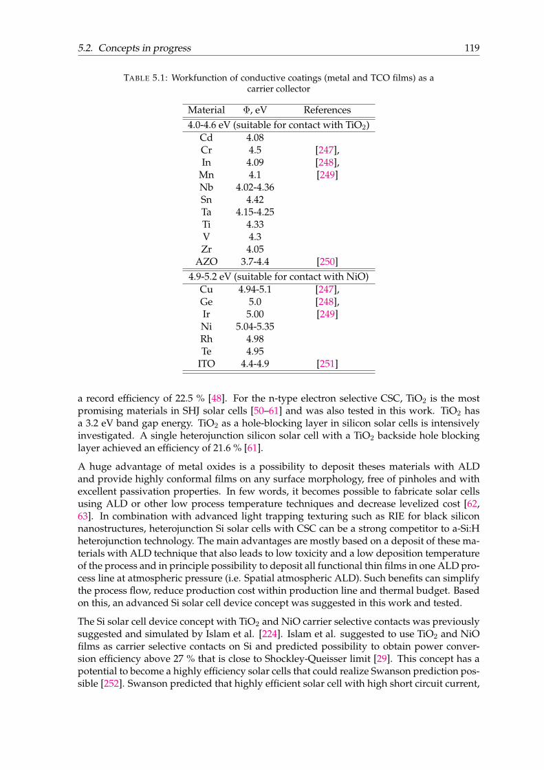
5.2. Concepts in progress 119
TABLE 5.1: Workfunction of conductive coatings (metal and TCO films) as acarrier collector
Material Φ, eV References4.0-4.6 eV (suitable for contact with TiO2)
Cd 4.08Cr 4.5 [247],In 4.09 [248],
Mn 4.1 [249]Nb 4.02-4.36Sn 4.42Ta 4.15-4.25Ti 4.33V 4.3Zr 4.05
AZO 3.7-4.4 [250]4.9-5.2 eV (suitable for contact with NiO)
Cu 4.94-5.1 [247],Ge 5.0 [248],Ir 5.00 [249]Ni 5.04-5.35Rh 4.98Te 4.95
ITO 4.4-4.9 [251]
a record efficiency of 22.5 % [48]. For the n-type electron selective CSC, TiO2 is the mostpromising materials in SHJ solar cells [50–61] and was also tested in this work. TiO2 hasa 3.2 eV band gap energy. TiO2 as a hole-blocking layer in silicon solar cells is intensivelyinvestigated. A single heterojunction silicon solar cell with a TiO2 backside hole blockinglayer achieved an efficiency of 21.6 % [61].
A huge advantage of metal oxides is a possibility to deposit theses materials with ALDand provide highly conformal films on any surface morphology, free of pinholes and withexcellent passivation properties. In few words, it becomes possible to fabricate solar cellsusing ALD or other low process temperature techniques and decrease levelized cost [62,63]. In combination with advanced light trapping texturing such as RIE for black siliconnanostructures, heterojunction Si solar cells with CSC can be a strong competitor to a-Si:Hheterojunction technology. The main advantages are mostly based on a deposit of these ma-terials with ALD technique that also leads to low toxicity and a low deposition temperatureof the process and in principle possibility to deposit all functional thin films in one ALD pro-cess line at atmospheric pressure (i.e. Spatial atmospheric ALD). Such benefits can simplifythe process flow, reduce production cost within production line and thermal budget. Basedon this, an advanced Si solar cell device concept was suggested in this work and tested.
The Si solar cell device concept with TiO2 and NiO carrier selective contacts was previouslysuggested and simulated by Islam et al. [224]. Islam et al. suggested to use TiO2 and NiOfilms as carrier selective contacts on Si and predicted possibility to obtain power conver-sion efficiency above 27 % that is close to Shockley-Queisser limit [29]. This concept has apotential to become a highly efficiency solar cells that could realize Swanson prediction pos-sible [252]. Swanson predicted that highly efficient solar cell with high short circuit current,

120 Chapter 5. Outlook and Guideline for Future Work
open circuit voltage and above 25 % power conversion efficiency could be realized with ef-ficient selective contacts, one for electron blocking and another for hole blocking. In thiscontext, TiO2 and NiO are almost perfect candidates. There materials have almost perfectenergy band alignment in conduction band (for TiO2) and valence band (for NiO) and hugevalence band barrier for holes at the TiO2-Si interface and conduction band barrier for elec-trons at the NiO-Si interface as shown in Fig. 5.5 and accordingly to Tab. 5.2. TiO2-Si andSi-NiO heterojunctions have either with p- or n-type equivalent to Si doping and thereforen-p, n-n and p-p and n-p heterojunctions. Corresponding properties of these materials arepresented in Tab. 5.2 [161]. These two thin films in conjunction have the same role as thep-n–junction in the conventional solar cell. The barrier from each CSCs should result in acurrent flow.
TABLE 5.2: Physical parameters of Si, TiO2 (anatase), NiO and a-Si semicon-ductor materials [161, 253]
Parameters Si TiO2(anatase)
NiO a-Si
Energy bandgap, Eg, eV 1.12 3.26 3.36 1.4-1.9Electron affinity, χ, eV 4.01 4.1 1.8 3.8Net donor doping, ND −NA 1018 1018 1018
Net acceptor doping, NA−ND 1018 1018 1018
Lattice constant, a, (Å) 5.431 a0=b0=3.785c0=9.514
a0=4.1758c0=5.213
NA
Dielectric constant, ε 12 86 11.75 11.8Electron mobility, µe,(cm2/(Vs))
1350 0.1 0.1 1
Hole mobility, µh, (cm2/(Vs)) 480 0.1 0.1 0.01Effective density of states(conduction band), NC,(cm−3)
2.8 × 10¹⁹ 7.93 × 10²⁰ 8.87 × 10¹⁸ 4.5 × 10²¹
Effective density of states (va-lence band), NV, (cm−3)
1.04 × 10¹⁹ 1.79 × 10¹⁹ 7.57 × 10¹⁸ 6.4 × 10²¹
Based on the presented solar cell concept with carrier selective TiO2-Si and Si-NiO hetero-junctions contacts, an advanced architecture on nanostructured Si solar cell was suggestedand presented in Fig. 5.6. Figure 5.7 shows the simplified process flow in order to fabri-cate the cell. More details process flow is attached as Appendix C. In order to increase theshort circuit current, light trapping texturing was employed for silicon wafers as a step (1).Texturing techniques and optimization process are presented in details in Chapter 4 andconsisted of three set of wafer: polished, KOH textured and RIE black Si textured. KOHtextured samples were processed for 50 min in 2 % KOH, 7 % IPA (HO2 solution) at 70 oCand RIE black Si with etching time - 14 min; pressure 38 mTorr; O2 100 sccm; SF6 70 sccm;power coil 3000 W; power platen 10 W, chiller temperature, -20 oC; etch rate - 98 nm/min.The second (2) step consists of ALD deposition of Al2O3 layer in order to suppress minoritycarrier recombination at the interface. ALD Al2O3 process was conducted with TMA andH2O precursors as described in Chapter 4 at 200 oC with 380 cycles, which resulted to 32 nmthick layer.
After deposition, Al2O3 films were annealed in N2 ambient at 400 oC for 30 min. The third(3) step was UV photolithography in order to prepare opening on the backside of the waferprior to NiO carrier selective film deposition (see Appendix C). Forth step was NiO depo-sition with RF sputtering from Ni target in Ar and O2 ambient leading to Ni oxidation in

5.2. Concepts in progress 121
FIGURE 5.5: Energy band diagram of proposed TiO2-Si-NiO solar cell
FIGURE 5.6: Structure of proposed TiO2-Si-NiO solar cell with all interlayersand CSCs
plasma and its deposition on Si wafer. NiO RF sputtering process was conducted at 20 %Ar/O2 ratio, power 20 W, pressure 5 mTorr, temperature 20 oC for 3 min and resulted in 15nm thick NiO film. Fifth step was Ni film electron beam deposition in order to obtain 5 nmthick film. Ni film was deposited with intention to adjust hole barrier height and Fermi leveldepinning [224]. The next step (6), Al with electron beam technique was deposited with athickness of 300 nm. The seventh step (7) included UV front side photolithography in orderto prepare opening on the backside of the wafer prior to TiO2 film growth. The eighth step(8) was ALD TiO2 growth at 80 oC with 110 cycles leading to 5 nm thick film. Post depositionannealing at 200 oC for 10 min was applied in order to improve TiO2 properties. Next andthe last step (9) was Ti film 5 nm thick deposition, in order to adjust hole barrier height andFermi level depinning [224], following with 300 nm Al film deposition with electron beamtechnique.
Figure 5.8 shows KOH textured and black Si textured fabricated solar cell with metal oxidecarrier selective contacts concept.
Characterization of the cell performance was evaluated under a sun simulator. The currentdensity -voltage (j-V) experimental results in dark and under one sun illumination (AM1.5G)

122 Chapter 5. Outlook and Guideline for Future Work
FIGURE 5.7: Process flow of proposed TiO2-Si-NiO solar cell with all interlay-ers and CSCs
FIGURE 5.8: Photoimages of fabricated solar cells: (a) KOH-textured solar celland (b) black Si RIE textured solar cell
for all cells obtained from each of the fabricated devices. However, only one selected illu-minated J-V curves for each type of cells (polished, KOH textured and black Si) are shown

5.3. Future work 123
FIGURE 5.9: J-V characteristic of fabricated solar cells on a polished, KOH-textured and black Si RIE textured substrate
in Fig. 5.9 since the other characteristic expressed similar behaviour. It is obvious fromFig. 5.9 that solar cell devices suffer from severe issues. Analysis of lifetime evolution dur-ing fabrication of solar cell batch led to conclusion that the causes of lifetime degradationis possible Al2O3 damage during photolithography steps, electron beam metal depositionand/or TMA precursor poor quality. The S-type varied J-V behaviour of the devices couldbe due to surface interface recombination difference, excessive defects in Al2O3 layer, de-fects in TiO2 layer due to electron beam deposited particles, ALD TiCl4 precursor impurity,defects in NiO layer due to RF sputtering induced damage on Si and oxygen vacancies ef-fect on NiO properties. In order to understand in details the causes, more comprehensiveanalysis is required. Detailed analysis including simulation of devices and comparison withexperimental device characterization, SEM and TEM study of metal oxides coating of tex-tured surfaces, external quantum efficiency in order to understand the carrier extractionissues, surface recombination analysis to understand losses at the interfaces, UPS and XPSstudy of heterojunctions in order to understand composition of deposited materials, oxygenvacancies and band alignment at the interfaces.
5.3 Future work
Metal oxide carrier selective contacts have an enormous potential for solar cells as a po-tentially cheap and reliable technology to advance the field. The goal of this thesis wasto identify the issue, challenges, and possible solutions. First – improvement of interfacepassivation, second – reliable device architecture, and third – testing and development of al-ternative materials as carrier selective passivating contacts. Alternative methods of surfacepassivation can be based on TiO2 and Al2O3 material and their ALD deposited stacks. Sec-tion 3.2 briefly discussed the possibility of using tunnelling oxides as an enhancement to the

124 Chapter 5. Outlook and Guideline for Future Work
interface passivation. The well-tested architecture could be simulated and tested with newmaterials like CSCs. The concept of such based HIT architecture is presented in Fig. 5.10,by replacing conventional CSC with metal oxides (TiO2 or NiO, etc.). Application of newmaterials based on perfect fit with silicon either conduction or valence band can guaranteelow interface defects, higher efficiency, and low-cost production technology. In Figure 5.11,brief summary of the most interesting and already tested metal oxide materials such as CSCand TCOs are shown.
FIGURE 5.10: Illustrations of IBC (a) front contact (b) SHJ solar cell with carrierselective transition metal oxides contacts and nanostructured (black Si) front
surface absorber
Electron conductive materials (TiO2, ZnO, Ta2O5) [50–61], transparent conductive oxides(AZO, ITO, IZO etc.)[232–234], hole conductive materials (NiO, MoO3, CuAlOx, V2O5, WO3etc.) [48–55], [56–60], [47] and tunneling passivation oxides (SiO2, Al2O3) are already ingood match with silicon (Fig. 5.11) to be tested in a heterojunction concept (Fig. 5.12). Thiswork was called to explore some of the concepts. However, there are numerous opportuni-ties that could be explored further with the materials mentioned above. Another interestingconcept is to test such carrier selective contacts with perovskite absorbers or in tandem withSi heterojunction solar cells.
5.4 ALD grown CSCs, passivation layers, ARC and TCO and in-dustrial potential
Furthermore, the above mentioned materials (TiO2, ZnO, Ta2O5, AZO, ITO, IZO, NiO, MoO3,CuAlOx, V2O5, WO3, SiO2, Al2O3) become even more interesting if all of them are depositedwith ALD techniques [254], which provides excellent quality of the films without any sur-face damage and even possibility for stack deposition; consequently, more efficient passi-vation of interfaces and tuning of material properties. During this PhD project, ALD hasshown as the most reliable thin film deposition technique, that allowed to deposit highlyconformal films on any simple and complex surface morphology, guarantee excellent sur-face passivation with different materials and precisely control film thickness. It is one of themost interesting topics for future work: application of ALD for deposition of carrier selec-tive and passivating materials in solar cell fabrication. Moreover, ALD has already gainedsome industrial interest, and there are several companies that manufacture industrial scaleALD equipment (Beneq, SoLayTec, Oxford Instruments, ALD NanoSolutions, Cambridge

5.4. ALD grown CSCs, passivation layers, ARC and TCO and industrial potential 125
FIGURE 5.11: Energy band gap of materials that have potential as a carrierselective contacts in silicon solar cells
FIGURE 5.12: Energy band diagram of heterojunction silicon solar cells withwide bandgap transition metal oxide carrier selective contacts
NanoTech, Encapsulix, Picosun etc.) focused for PV applications. Such equipment can re-place almost all high-temperature processing equipment in the solar cell production line(Fig. 5.13). Consequently, industrial ALD process development for PV industry acquired a

126 Chapter 5. Outlook and Guideline for Future Work
new interesting turn and opportunities to explore. Now the time to show a proof of conceptdevices with ALD deposited layers in solar cell.
FIGURE 5.13: ALD industrial equipment as an alternative to the conven-tional high-temperature process production line. Note: red cross indicates
the equipment which could be replaced with ALD
In addition, the newest concepts in ALD development, such as spacial atmospheric ALD,combine the advantage of temporal ALD, excellent control of film composition, conformal-ity and uniformity at atmospheric pressure and at low temperatures with a deposition rateapproaching 100 nm per min. In this sense, ALD start to compete with other well estab-lished thin film deposition techniques particularly in PV industry and not only. No doubt,ALD is the future technology for precise thin film growth and worth to explore!

127
Bibliography
[1] J. Melorose, R. Perroy, and S. Careas. “World population prospects”. In: United Na-tions 1.6042 (2015), pp. 587–92. DOI: 10.1017/CBO9781107415324.004.
[2] Arno H. M. Smets et al. Solar energy: the physics and engineering of photovoltaic conver-sion, technologies and systems. UIT Cambridge Ltd., 2016.
[3] U.S. Energy Information Administration. International Energy Outlook 2016. Vol. 0484(2016).May 2016. 2016, pp. 1–2. DOI: www.eia.gov/forecasts/ieo/pdf/0484(2016).pdf.
[4] Worldometers. World Population Clock. 2017. URL: http://www.worldometers.info/world-population/.
[5] British Petroleum. BP energy outlook 2016. Tech. rep. 9. 2016, pp. 1689–1699. DOI: 10.1017/CBO9781107415324.004.
[6] Joel E Cohen. “Human Population: The Next Half Century”. In: Science 302.5648(2003), pp. 1172–1175. DOI: 10.1126/science.1088665.
[7] Robert A. Rohde. “Global Warming Art”. In: (June 2011). URL: http://www.globalwarmingart.com.
[8] IPCC. “Climate Change 2013: The Physical Science Basis”. In: Climate Change 2013.2013, p. 1535. DOI: 10.1017/CBO9781107415324.
[9] Christoph Kost et al. “Levelized Cost of Electricity Renewable Energy Technologies”.In: Fraunhofer Institut for Solar Energy Systems ISE Levelized November (2013), p. 50.DOI: 10.1613/jair.301.
[10] Solar Power Europe. Global Market Outlook for Solar Power 2016-2020. Tech. rep. 2016.[11] Kunta Yoshikawa et al. “Silicon heterojunction solar cell with interdigitated back con-
tacts for a photoconversion efficiency over 26%”. In: Nature Energy 2.17032 (2017).DOI: 10.1038/nenergy.2017.32.
[12] Steven Bushong. “Futurist Ray Kurzweil predicts solar industry dominance in 12years”. In: Solar Power World 3.30 (2016), p. 063301.
[13] Fraunhofer ISE. “Photovoltaics Report”. In: August (2015).[14] Pietro Altermatt. Altermatt’s Lectures on Photovoltaics. 2017. URL: https://www.
pvlighthouse.com.au/cms/lectures/altermatt/ (visited on 10/28/2017).[15] NREL. Reference Solar Spectral Irradiance: Air Mass 1.5. 2017. URL: http://rredc.
nrel.gov/solar/spectra/am1.5/ (visited on 10/28/2017).[16] Newport. Solar Radiation. 2017. URL: https://www.newport.com/t/introduction-
to-solar-radiation (visited on 10/28/2017).[17] SOLARGIS. Global Horizontal Irradiation (GHI) map. 2017. URL: http://solargis.
com/products/maps-and-gis-data/free/download/world (visited on10/28/2017).
[18] A. Becquerel. “Mémoire sur les effets électriques produits sous linfluence des rayonssolaires”. In: Comptes rendus 9 (1839), 561–567. DOI: 10.1109/PVSC.2016.7750356.
[19] Peter Würfel. Physics of Solar Cells. Weinheim, Germany: Wiley-VCH Verlag GmbH,2005, pp. 1 –186. DOI: 10.1002/9783527618545.
[20] M A Green, A Ho-Baillie, and H J Snaith. “The emergence of perovskite solar cells”.In: Nature Photonics 8.7 (2014). DOI: Doi10.1038/Nphoton.2014.134.

128 BIBLIOGRAPHY
[21] S. Smit et al. “Metal-oxide-based hole-selective tunneling contacts for crystalline sil-icon solar cells”. In: Solar Energy Materials and Solar Cells 120.PART A (2014). DOI:10.1016/j.solmat.2013.06.016.
[22] Frank Feldmann et al. “Tunnel oxide passivated contacts as an alternative to partialrear contacts”. In: Solar Energy Materials and Solar Cells 131 (2014). DOI: 10.1016/j.solmat.2014.06.015.
[23] pvEducation recombination. http://pveducation.org/pvcdrom/characterisation/surface-recombination. Accessed: 2017-06-23. surface-recombination.
[24] pvEducation lifetime. http://pveducation.org/pvcdrom/pn- junction/lifetime. Accessed: 2016-06-23.
[25] M. A. Green. “Solar cell fill factors: General graph and empirical expressions”. In:Solid-State Electronics 24 (1981), pp. 788 –789. DOI: 10.1016/0038- 1101(81)90062-9.
[26] National Renewable Energy Laboratory. Best Research-Cell Efficiencies. 2017. URL: https://www.nrel.gov/pv/assets/images/efficiency-chart.png (visited on10/28/2017).
[27] Wiley. Progress in Photovoltaics: Research and Applications. 2017. URL: http://onlinelibrary.wiley.com/journal/10.1002/(ISSN)1099-159X (visited on 10/28/2017).
[28] Martin A. Green et al. “Solar cell efficiency tables (version 50)”. In: Progress in Pho-tovoltaics: Research and Applications 25.7 (2017). PIP-17-089, pp. 668–676. ISSN: 1099-159X. DOI: 10.1002/pip.2909.
[29] William Shockley, Hans Queisser, and Hans J Queisser. “The Shockley-Queisser limit”.In: Journal of Applied Physics 32 (1961), pp. 510–519.
[30] Louise C. Hirst and Nicholas J. Ekins-Daukes. “Fundamental losses in solar cells”.In: Progress in Photovoltaics 19.3 (2011), pp. 286–293. DOI: 10.1002/pip.1024.
[31] Martin A. Green. “The path to 25 % silicon solar cell efficiency: History of silicon cellevolution”. In: Progress in Photovoltaics: Research and Applications 17.3 (2009), pp. 183–189. DOI: 10.1002/pip.892.
[32] Simeon C. Baker-Finch and Keith R. McIntosh. “Reflection of normally incident lightfrom silicon solar cells with pyramidal texture”. In: Progress in Photovoltaics: Researchand Applications 19.4 (2011), pp. 406–416. DOI: 10.1002/pip.1050.
[33] Gerhard Bauer. “Absolutwerte der optischen Absorptionskonstanten von Alkalihalo-genidkristallen im Gebiet ihrer ultravioletten Eigenfrequenzen”. In: Annalen der Physik411 (1934), pp. 434 –464. DOI: 10.1002/(ISSN)1521-388910.1002/andp.v411:410.1002/andp.19344110405.
[34] M. A. Green. Solar Cells - Operating Principles, Technology and System Application. Kens-ington, Australia: University of New South Wales, 1992.
[35] Martin Otto et al. “Black silicon photovoltaics”. In: Advanced Optical Materials 3.2(2015), pp. 147–164. DOI: 10.1002/adom.201400395.
[36] Stefaan De Wolf et al. “High-efficiency Silicon Heterojunction Solar Cells: A Review”.In: Green 2.1 (2012), pp. 7–24. DOI: 10.1515/green-2011-0039.
[37] “Achievement of More Than 25% Conversion Efficiency With Crystalline Silicon Het-erojunction Solar Cell”. In: IEEE Journal of Photovoltaics 4.6 (2014), pp. 1433–1435. DOI:10.1109/JPHOTOV.2014.2352151.
[38] U. Würfel, A. Cuevas, and P. Würfel. “Charge Carrier Separation in Solar Cells”. In:IEEE Journal of Photovoltaics 5.1 (2015), pp. 461–469. DOI: 10.1109/JPHOTOV.2014.2363550.
[39] David L. Young et al. “Carrier selective, passivated contacts for high efficiency siliconsolar cells based on transparent conducting oxides”. In: 2014 IEEE 40th PhotovoltaicSpecialist Conference (PVSC). Vol. 55. 2014, pp. 1–5. DOI: 10.1109/PVSC.2014.6925147.

BIBLIOGRAPHY 129
[40] Frank Feldmann et al. “Efficient carrier-selective p- and n-contacts for Si solar cells”.In: Solar Energy Materials and Solar Cells 131 (2014), pp. 100–104. DOI: 10.1016/j.solmat.2014.05.039.
[41] Mikio Taguchi et al. “24.7% Record efficiency HIT solar cell on thin silicon wafer”. In:IEEE Journal of Photovoltaics 4.1 (2014), pp. 96–99. DOI: 10.1109/JPHOTOV.2013.2282737.
[42] A. Terakawa. “Review of thin-film silicon deposition techniques for high-efficiencysolar cells developed at Panasonic/Sanyo”. In: Solar Energy Materials and Solar Cells119 (2013). Thin-film Photovoltaic Solar Cells, pp. 204 –208. DOI: http://dx.doi.org/10.1016/j.solmat.2013.06.044.
[43] Martin Schaper et al. “20.1%-efficient crystalline silicon solar cell with amorphoussilicon rear-surface passivation”. In: Progress in Photovoltaics: Research and Applications13.5 (2005), pp. 381–386. DOI: 10.1002/pip.641.
[44] Xinbo Yang et al. “High-Performance TiO2-Based Electron-Selective Contacts for Crys-talline Silicon Solar Cells”. In: Advanced Materials 28.28 (2016), pp. 5891–5897. DOI:10.1002/adma.201600926.
[45] Bart Macco. “Status and prospects for atomic layer deposited metal oxide thin filmsin passivating contacts for c-Si photovoltaics”. In: 2016 IEEE 43rd Photovoltaic Special-ists Conference (PVSC) 9 (2016). DOI: 10.1109/PVSC.2016.7750088.
[46] Jens Meyer et al. Transition metal oxides for organic electronics: Energetics, device physicsand applications. 2012. DOI: 10.1002/adma.201201630.
[47] Luis G. Gerling et al. “Transition metal oxides as hole-selective contacts in silicon het-erojunctions solar cells”. In: Solar Energy Materials and Solar Cells 145 (2016), pp. 109–115. DOI: 10.1016/j.solmat.2015.08.028.
[48] Jonas Geissbühler et al. “22.5% efficient silicon heterojunction solar cell with molyb-denum oxide hole collector”. In: Applied Physics Letters 107.8 (2015). DOI: 10.1063/1.4928747.
[49] Corsin Battaglia et al. “Hole selective MoOx contact for silicon solar cells”. In: Nanoletters 14.2 (2014), pp. 967–71. DOI: 10.1021/nl404389u.
[50] Corsin Battaglia et al. “Hole selective MoOx contact for silicon heterojunction solarcells”. In: 2014 IEEE 40th Photovoltaic Specialist Conference, PVSC 2014. 2014, pp. 968–970. DOI: 10.1109/PVSC.2014.6925074.
[51] B. Macco et al. “Low-temperature atomic layer deposition of MoO x for silicon het-erojunction solar cells”. In: physica status solidi (RRL) - Rapid Research Letters 9.7 (2015),pp. 393–396. DOI: 10.1002/pssr.201510117.
[52] Martin Bivour et al. “Molybdenum and tungsten oxide: High work function wideband gap contact materials for hole selective contacts of silicon solar cells”. In: SolarEnergy Materials and Solar Cells 142 (2015), pp. 34–41. DOI: 10.1016/j.solmat.2015.05.031.
[53] James Bullock et al. “Molybdenum oxide MoOx: A versatile hole contact for siliconsolar cells”. In: Applied Physics Letters 105.23 (2014). DOI: 10.1063/1.4903467.
[54] James Bullock et al. “N- and p-typesilicon Solar Cells with Molybdenum Oxide HoleContacts”. In: Energy Procedia. Vol. 77. 2015. DOI: 10.1016/j.egypro.2015.07.063.
[55] Corsin Battaglia et al. “Silicon heterojunction solar cell with passivated hole selectiveMoOx contact”. In: Applied Physics Letters 104.11 (2014), p. 113902. DOI: 10.1063/1.4868880.
[56] Raisul Islam, Gautam Shine, and Krishna C. Saraswat. “Schottky barrier height re-duction for holes by Fermi level depinning using metal/nickel oxide/silicon con-tacts”. In: Applied Physics Letters 105.18 (2014), p. 182103. DOI: 10.1063/1.4901193.

130 BIBLIOGRAPHY
[57] Xingtian Yin et al. “19.2% Efficient InP Heterojunction Solar Cell with Electron-SelectiveTiO2 Contact”. In: ACS Photonics 1.12 (2014), pp. 1245–1250. DOI: 10.1021/ph500153c.
[58] Zu-Po Yang et al. “Atomic Layer Deposition TiO2 Films and TiO2/SiNx Stacks Ap-plied for Silicon Solar Cells”. In: Applied Sciences 6.8 (2016), p. 233. DOI: 10.3390/app6080233.
[59] Ken Alfred Nagamatsu. “Crystalline silicon photovoltaics via low-temperature TiO2/Siand PEDOT/Si heterojunctions.” In: Thesis (Ph.D.)–Princeton University, 2016.; Publi-cation Number: AAT 10010662 January (2016).
[60] Sushobhan Avasthi et al. “Double-heterojunction crystalline silicon solar cell fabri-cated at 250 C with 12.9 % efficiency”. In: 2014 IEEE 40th Photovoltaic Specialist Con-ference, PVSC 2014 (2014), pp. 949–952. DOI: 10.1109/PVSC.2014.6925069.
[61] Xinbo Yang et al. “High-Performance TiO2-Based Electron-Selective Contacts for Crys-talline Silicon Solar Cells”. In: Advanced Materials (2016), pp. 5891–5897. DOI: 10.1002/adma.201600926.
[62] Bart Macco. “Status and prospects for atomic layer deposited metal oxide thin filmsin passivating contacts for c-Si photovoltaics”. In: 2016 Ieee 43rd Photovoltaic SpecialistsConference (pvsc) September (2016). DOI: 10.1109/PVSC.2016.7750088.
[63] B. W. H. van de Loo et al. “Atomic-layer deposited passivation schemes for c-Si solarcells”. In: 2016 IEEE 43rd Photovoltaic Specialists Conference (PVSC). 2016, pp. 3655–3660. DOI: 10.1109/PVSC.2016.7750356.
[64] J.M. Ziman. Electrons and phonons: the theory of transport phenomena in solids. Vol. 20.New York: Oxford University Press, 1960, pp. xiv + 554. DOI: 10.1016/0160-9327(61)90046-1.
[65] Dragica Vasileska. Drift-Diffusion Model, Part A: Introduction. June 2006. URL: https://nanohub.org/resources/1511.
[66] PV Education. 2017. URL: http://www.pveducation.org/.[67] Martin A. Green and Mark J. Keevers. “Optical properties of intrinsic silicon at 300
K”. In: Progress in Photovoltaics: Research and Applications 3.3 (1995), pp. 189–192. DOI:10.1002/pip.4670030303.
[68] J. Dziewior and W. Schmid. “Auger coefficients for highly doped and highly excitedsilicon”. In: Applied Physics Letters 31.5 (1977), pp. 346–348. DOI: 10.1063/1.89694.
[69] R. N. Hall. “Electron-Hole Recombination in Germanium”. In: Phys. Rev. 87 (2 1952),pp. 387–387. DOI: 10.1103/PhysRev.87.387.
[70] W. Shockley and W. T. Read. “Statistics of the Recombinations of Holes and Elec-trons”. In: Phys. Rev. 87 (5 1952), pp. 835–842. DOI: 10.1103/PhysRev.87.835.
[71] Armin Richter et al. “Improved quantitative description of Auger recombination incrystalline silicon”. In: Physical Review B - Condensed Matter and Materials Physics 86.16(2012). DOI: 10.1103/PhysRevB.86.165202.
[72] Sara Olibet, Evelyne Vallat-Sauvain, and Christophe Ballif. “Model for a-Si:H/c-Siinterface recombination based on the amphoteric nature of silicon dangling bonds”.In: Physical Review B - Condensed Matter and Materials Physics 76.3 (2007). DOI: 10.1103/PhysRevB.76.035326.
[73] Armin Richter et al. “Improved quantitative description of Auger recombination incrystalline silicon”. In: Physical Review B 86.16 (2012), p. 165202. DOI: 10.1103/PhysRevB.86.165202.
[74] Jihun Oh, Hao-Chih Yuan, and Howard M. Branz. “An 18.2%-efficient black-siliconsolar cell achieved through control of carrier recombination in nanostructures”. In:Nature nanotechnology 7.11 (2012), pp. 743–748. DOI: 10.1038/nnano.2012.166.
[75] Martin Otto et al. “Extremely low surface recombination velocities in black siliconpassivated by atomic layer deposition”. In: Applied Physics Letters 100.191603 (2012),pp. 1–5. DOI: 10.1063/1.4714546.

BIBLIOGRAPHY 131
[76] Keith McIntosh, Malcolm Abbott, and Ben Sudbury. PV Lighthouse. 2017. URL: https://www.pvlighthouse.com.au/.
[77] B. Swatowska et al. “The role of antireflective coatings in silicon solar cells - Theinfluence on their electrical parameters”. In: Optica Applicata 41.2 (2011), pp. 487–492.
[78] Andrew F Thomson and Keith R McIntosh. “Light-enhanced surface passivation ofTiO2-coated silicon”. In: Progress in Photovoltaics: Research and Applications 20.3 (2012),pp. 343–349. DOI: 10.1002/pip.1132.
[79] Christian Stefano Schuster. Diffractive Optics for Thin-Film Silicon Solar Cells. SpringerInternational Publishing, 2017.
[80] J. I. Gittleman et al. “Textured silicon: A selective absorber for solar thermal conver-sion”. In: Applied Physics Letters 35.10 (1979), pp. 742–744. DOI: 10.1063/1.90953.
[81] W H Southwell. “Gradient-index antireflection coatings.” In: Optics letters 8.11 (1983),pp. 584–586. DOI: 10.1364/OL.8.000584.
[82] C. C. Striemer and P. M. Fauchet. “Dynamic etching of silicon for broadband an-tireflection applications”. In: Applied Physics Letters 81.16 (2002), pp. 2980–2982. DOI:10.1063/1.1514832.
[83] Eli Yablonovitch. “Statistical ray optics”. In: Journal of the Optical Society of America72.7 (1982), p. 899. DOI: 10.1364/JOSA.72.000899.
[84] V. Ganapati, O. D. Miller, and E. Yablonovitch. “Light Trapping Textures Designed byElectromagnetic Optimization for Subwavelength Thick Solar Cells”. In: IEEE Journalof Photovoltaics 4.1 (2014), pp. 175–182. DOI: 10.1109/JPHOTOV.2013.2280340.
[85] Bennett W. Schneider et al. “Pyramidal surface textures for light trapping and antire-flection in perovskite-on-silicon tandem solar cells”. In: Optical Express 22.S6 (2014),A1422–A1430. DOI: 10.1364/OE.22.0A1422.
[86] Maksym Plakhotnyuk et al. “Lifetime of Nano-Structured Black Silicon for Photo-voltaic Applications”. In: Proceeding of the 32nd European Photovoltaic Solar Energy Con-ference and Exhibition. Munich, 2016, pp. 1–4. URL: http://www.forskningsdatabasen.dk/en/catalog/2307186226.
[87] V.F. Onyshchenko et al. “Effective lifetime of minority carriers in black silicon nano-textured by cones and pyramids”. In: Semiconductor Physics, Quantum Electronics Op-toelectronics 20.3 (2017), p. 325. DOI: https://doi.org/10.15407/spqeo20.03.325.
[88] Yi-Fan Huang et al. “Improved broadband and quasi-omnidirectional anti-reflectionproperties with biomimetic silicon nanostructures”. In: Nature Nanotechnology 2.12(2007), pp. 770–774. DOI: 10.1038/nnano.2007.389.
[89] Matthias Kroll et al. “Black silicon for solar cell applications”. In: Proc. SPIE. Ed.by Ralf Wehrspohn and Andreas Gombert. Vol. 8438. 8438-42. 2012, p. 843817. DOI:10.1117/12.922380.
[90] Martin Otto. “Effective Passivation of Black Silicon Surfaces by Conformal ThermalALD Deposited Al2O3 Layers. Ph.D. Thesis”. PhD thesis. Halle-Salle: Martin-Luther-Universitat Halle-Wittenberg, 2015, p. 161.
[91] Loucas Tsakalakos. “Nanostructures for photovoltaics”. In: Materials Science and En-gineering R-reports 62.6 (2008), pp. 175–189. DOI: 10.1016/j.mser.2008.06.002.
[92] Thomas J. Kempa et al. “Single and Tandem Axial p-i-n Nanowire Photovoltaic De-vices”. In: Nano Letters 8.10 (2008), pp. 3456–3460. DOI: 10.1021/nl8023438.
[93] J. Gwamuri, D. Ö. Güney, and J. M. Pearce. “Advances in Plasmonic Light Trappingin Thin-Film Solar Photovoltaic Devices”. In: Solar Cell Nanotechnology. John Wiley &Sons, Inc., 2013, pp. 241–269. DOI: 10.1002/9781118845721.ch10.
[94] Pierpaolo Spinelli and Albert Polman. “Light Trapping in Thin Crystalline Si So-lar Cells Using Surface Mie Scatterers”. In: IEEE Journal of Photovoltaics 4.2 (2014),pp. 554–559. DOI: 10.1109/JPHOTOV.2013.2292744.

132 BIBLIOGRAPHY
[95] Claire van Lare et al. “Dielectric Scattering Patterns for Efficient Light Trapping inThin-Film Solar Cells”. In: Nano Letters 15.8 (2015), pp. 4846–4852. DOI: 10.1021/nl5045583.
[96] Hua-Min Li et al. “Enhancement of light absorption using high-k dielectric in local-ized surface plasmon resonance for silicon-based thin film solar cells”. In: Journal ofApplied Physics 109.9 (2011), p. 093516. DOI: 10.1063/1.3587165.
[97] D.M. Chapin, C.S. Fuller, and G.L. Pearson. “A new silicon p-n junction photocell forconverting solar radiation into electrical power”. In: Journal of Applied Physics 25(5)(1954), p. 676.
[98] P. T. Landsberg. “Introduction to the theory of photovoltaic cells”. In: Solid-state Elec-tron 18.12 (1975), pp. 1043–1052.
[99] R.J. Handy. “Theoretical analysis of the series resistance of a solar cell”. In: Solid-StateElectronics 10.8 (1967), pp. 765 –775. DOI: http://dx.doi.org/10.1016/0038-1101(67)90159-1.
[100] William Shockley and Hans J. Queisser. “Detailed balance limit of efficiency of p-n junction solar cells”. In: Journal of Applied Physics 32.3 (1961), pp. 510–519. DOI:10.1063/1.1736034.
[101] Jianhua Zhao, Aihua Wang, and Martin A. Green. “24.5% Efficiency PERT siliconsolar cells on SEH MCZ substrates and cell performance on other SEH CZ and FZsubstrates”. In: Solar Energy Materials and Solar Cells 66.1-4 (2001), pp. 27–36. DOI:10.1016/S0927-0248(00)00155-0.
[102] R.L. Anderson. “Experiments on Ge-GaAs heterojunctions”. In: Solid-State Electronics5.5 (1962), pp. 341 –351. DOI: http://dx.doi.org/10.1016/0038-1101(62)90115-6.
[103] W. R. Frensley and H. Kroemer. “Theory of the energy-band lineup at an abruptsemiconductor heterojunction”. In: Physical Review B 16.6 (1977), pp. 2642–2652. DOI:10.1103/PhysRevB.16.2642.
[104] Walter A. Harrison. “Elementary theory of heterojunctions”. In: Journal of VacuumScience and Technology 14.4 (1977), pp. 1016–1021. DOI: 10.1116/1.569312.
[105] M.J. Adams and Allen Nussbaum. “A proposal for a new approach to heterojunctiontheory”. In: Solid-State Electronics 22.9 (1979), pp. 783 –791. DOI: http://dx.doi.org/10.1016/0038-1101(79)90127-8.
[106] Oldwig von Ross. “Theory of extrinsic and intrinsic heterojunctions in thermal equi-librium”. In: Solid-State Electronics 23.10 (1980), pp. 1069 –1075. DOI: http://dx.doi.org/10.1016/0038-1101(80)90187-2.
[107] J. Tersoff. “Theory of semiconductor heterojunctions: The role of quantum dipoles”.In: Physical Review B 30.8 (1984), pp. 4874–4877. DOI: 10.1103/PhysRevB.30.4874.
[108] A.G. Milnes, and D.L. Feucht. Academic Press, 1972, pp. iii –. DOI: https://doi.org/10.1016/B978-0-12-498050-1.50001-0.
[109] Sushobhan Avasthi et al. “Hole-blocking titanium-oxide/silicon heterojunction andits application to photovoltaics”. In: Applied Physics Letters 102.20 (2013). DOI: 10.1063/1.4803446.
[110] Raisul Islam, Krishna C. Saraswat, and Electrical Engineering. “Metal/insulator/semi-conductor carrier selective contacts for photovoltaic cells”. In: IEEE 40th PhotovoltaicSpecialist Conference (PVSC). 2014, pp. 285–289. DOI: 10.1109/PVSC.2014.6924915.
[111] Yimao Wan, James Bullock, and Andres Cuevas. “Tantalum oxide/silicon nitride:A negatively charged surface passivation stack for silicon solar cells”. In: AppliedPhysics Letters 106.20 (2015), p. 201601. DOI: 10.1063/1.4921416.

BIBLIOGRAPHY 133
[112] B. Hussain, A. Ebong, and I. Ferguson. “Zinc oxide and silicon based heterojunctionsolar cell model”. In: 2015 IEEE 42nd Photovoltaic Specialist Conference (PVSC). June2015, pp. 1–4. DOI: 10.1109/PVSC.2015.7356242.
[113] MeiKei Ieong et al. “Comparison of raised and Schottky source/drain MOSFETsusing a novel tunneling contact model”. In: International Electron Devices Meeting1998. Technical Digest (Cat. No.98CH36217). 1998, pp. 733–736. DOI: 10.1109/IEDM.1998.746461.
[114] H. Steinkemper et al. “Numerical Simulation of Carrier-Selective Electron ContactsFeaturing Tunnel Oxides”. In: IEEE Journal of Photovoltaics 5.5 (2015), pp. 1348–1356.DOI: 10.1109/jphotov.2015.2455346.
[115] H. Watanabe, D. Matsushita, and K. Muraoka. “Determination of tunnel mass andphysical thickness of gate oxide including poly-Si/SiO2 and Si/SiO2 interfacial tran-sition Layers”. In: IEEE Transactions on Electron Devices 53.6 (2006), pp. 1323–1330.DOI: 10.1109/TED.2006.874749.
[116] M. Zemanová Diešková, A. Ferretti, and P. Bokes. “Tunneling through Al/AlOx/Aljunction: Analytical models and first-principles simulations”. In: Physical Review B 87(19 2013), p. 195107. DOI: 10.1103/PhysRevB.87.195107.
[117] R. Tsu and L. Esaki. “Tunneling in a finite superlattice”. In: Applied Physics Letters22.11 (1973), pp. 562–564. DOI: 10.1063/1.1654509.
[118] Maksym M. Plakhotnyuk et al. “Surface passivation and carrier selectivity of thethermal-atomic-layer-deposited TiO2 on crystalline silicon”. In: Japanese Journal of Ap-plied Physics 56.8S2 (2017), 08MA11. DOI: 10.7567/jjap.56.08ma11.
[119] G. San Vicente, A. Morales, and M. T. Gutierrez. “Preparation and characterizationof sol-gel TiO2 antireflective coatings for silicon”. In: Thin Solid Films 391.1 (2001),pp. 133–137. DOI: 10.1016/S0040-6090(01)00963-4.
[120] / N-Si Heterojunction et al. “Photovoltaic Behaviors in an Isotype n-TiO2/n-Si Het-erojunction Photovoltaic Behaviors in an Isotype n-TiO”. In: Chinese Phys. Lett. PHYS.LETT 28.12 (2011), pp. 2–4. DOI: 10.1088/0256-307X/28/12/127305.
[121] Markku Leskelä and Mikko Ritala. “Atomic layer deposition (ALD): From precursorsto thin film structures”. In: Thin Solid Films 409.1 (2002), pp. 138–146. DOI: 10.1016/S0040-6090(02)00117-7.
[122] Xingtian Yin et al. “19.2% Efficient InP Heterojunction Solar Cell with Electron-SelectiveTiO2 Contact”. In: ACS Photonics 1.12 (2014), pp. 1245–1250. DOI: 10.1021/ph500153cM4-Citavi.
[123] Weitse Hsu et al. “Electron-Selective TiO2 Contact for Cu(In,Ga)Se2 Solar Cells”. In:Scientific Reports 5 (2015), p. 16028. DOI: 10.1038/srep16028.
[124] D. Vossing et al. “Heterojunction Solar Cell with Titanium Dioxide Nanolayer withan Efficiency of 10.1%”. In: 43th IEEE Photovoltaic Specialists Conference (2016), inpress. DOI: 10.1109/PVSC.2016.7750104.
[125] Xinbo Yang and Klaus Weber. “N-type silicon solar cells featuring an electron-selectiveTiO2 contact”. In: 2015 IEEE 42nd Photovoltaic Specialist Conference (PVSC). Vol. 42.IEEE, 2015, pp. 1–4. DOI: 10.1109/PVSC.2015.7356139.
[126] Xinbo Yang et al. “Silicon heterojunction solar cells with electron selective TiOx con-tact”. In: Solar Energy Materials and Solar Cells 150 (2016), pp. 32–38. DOI: 10.1016/j.solmat.2016.01.020.
[127] Ken A. Nagamatsu et al. “Titanium dioxide/silicon hole-blocking selective contact toenable double-heterojunction crystalline silicon-based solar cell”. In: Applied PhysicsLetters 106.12 (2015), pp. 0–5. DOI: 10.1063/1.4916540.
[128] Jie Cui et al. “Titanium oxide: A re-emerging optical and passivating material forsilicon solar cells”. In: Solar Energy Materials and Solar Cells 158 (2016), pp. 115–121.DOI: 10.1016/j.solmat.2016.05.006.

134 BIBLIOGRAPHY
[129] S. Avasthi et al. “Hole-blocking TiO2/Silicon Heterojunction for Silicon PhotovoItaics”.In: Device Research Conference (DRC), 2012 70th Annual (2012), p. 93. DOI: 10.1109/DRC.2012.6256955.
[130] Janam Jhaveri et al. “Stable low-recombination n-Si/TiO2 hole-blocking interface andits effect on silicon heterojunction photovoltaics”. In: 2014 IEEE 40th Photovoltaic Spe-cialist Conference (PVSC). IEEE, 2014, pp. 1525–1528. DOI: 10.1109/PVSC.2014.6925206.
[131] Ing-Song Yu et al. “Surface Passivation of c-Si by Atomic Layer Deposition TiO2 ThinFilms Deposited at Low Temperature”. In: IEEE 40th Photovoltaic Specialist Conference(PVSC). 100. 2014, pp. 1271–1274. DOI: 10.1109/PVSC.2014.6925148.
[132] Benjamin G. Lee et al. “Excellent passivation and low reflectivity Al2O3 /TiO2 bi-layer coatings for n-wafer silicon solar cells”. In: Conference Record of the IEEE Photo-voltaic Specialists Conference June (2012), pp. 1066–1068. DOI: 10.1109/PVSC.2012.6317787.
[133] Gijs Dingemans and W.M.M. Kessels. “Aluminum Oxide and Other ALD Materialsfor Si Surface Passivation”. In: ECS Transactions 41.2 (2011), pp. 293–301. DOI: 10.1149/1.3633680.
[134] B. S. Richards, J. E. Cotter, and C. B. Honsberg. “Enhancing the surface passivation ofTiO[sub 2] coated silicon wafers”. In: Applied Physics Letters 80.7 (2002), p. 1123. DOI:10.1063/1.1445810.
[135] P. Spinelli et al. “Al2O3/TiO2 nano-pattern antireflection coating with ultralow sur-face recombination”. In: Applied Physics Letters 102.23 (2013), p. 233902. DOI: 10.1063/1.4810970.
[136] Karim Mohamed Gad et al. “Ultrathin titanium dioxide nanolayers by atomic layerdeposition for surface passivation of crystalline silicon”. In: IEEE Journal of Photo-voltaics 6.3 (2016). DOI: 10.1109/JPHOTOV.2016.2545404.
[137] Dongchul Suh, Duk Yong Choi, and Klaus J. Weber. “Al2O3/TiO2 stack layers foreffective surface passivation of crystalline silicon”. In: Journal of Applied Physics 114.15(2013). DOI: 10.1063/1.4825258.
[138] Mingzheng Ge et al. “A review of one-dimensional TiO2 nanostructured materialsfor environmental and energy applications”. In: Journal of Material Chemistry A 4 (182016), pp. 6772–6801. DOI: 10.1039/C5TA09323F.
[139] Sushobhan Avasthi et al. “Hole-blocking titanium-oxide/silicon heterojunction andits application to photovoltaics”. In: Applied Physics Letters 102.20 (2013). DOI: 10.1063/1.4803446.
[140] J. H. Kim, S. Lee, and H. S. Im. “The effect of different ambient gases, pressures,and substrate temperatures on TiO2 thin films grown on Si(100) by laser ablationtechnique”. In: Applied Physics A: Materials Science and Processing 69.7 (1999). DOI:10.1007/s003399900208.
[141] Jaan Aarik et al. “Effect of crystal structure on optical properties of TiO2 films grownby atomic layer deposition”. In: Thin Solid Films 305.1-2 (1997), pp. 270–273. DOI:10.1016/S0040-6090(97)00135-1.
[142] Tuomo Suntola and Jaakko Hyvarinen. “Atomic Layer Epitaxy”. In: Annual Reviewof Materials Science 15.1 (1985), pp. 177–195. DOI: 10.1146/annurev.ms.15.080185.001141.
[143] Riikka L Puurunen and Riikka L Puurunen. “Surface chemistry of atomic layer depo-sition: A case study for the trimethylaluminum/water process”. In: Journal of AppliedPhysics 97.12 (2005), p. 121301. DOI: 10.1063/1.1940727.
[144] Mikko Ritala and Jaakko Niinistö. “Atomic Layer Deposition”. In: Chemical VapourDeposition: Precursors, Processes and Applications. 2009, pp. 158–206.

BIBLIOGRAPHY 135
[145] Mikko Ritala and Markku Leskelä. “Handbook of Thin Film Materials”. In: Handbookof Thin Film Materials. Vol. 1. 2002, pp. 103–159. DOI: 10.1016/B978-012512908-4/50005-9.
[146] Tuomo Suntola. “Surface chemistry of materials deposition at atomic layer level”. In:Applied Surface Science 100 (1996), pp. 391 –398. DOI: http://dx.doi.org/10.1016/0169-4332(96)00306-6.
[147] Janne-Petteri Niemelä, Giovanni Marin, and Maarit Karppinen. “Titanium dioxidethin films by atomic layer deposition: a review”. In: Semiconductor Science and Tech-nology (2017). URL: http://iopscience.iop.org/10.1088/1361-6641/aa78ce.
[148] Jaan Aarik et al. “Morphology and structure of TiO2 thin films grown by atomic layerdeposition”. In: Journal of Crystal Growth 148.3 (1995), pp. 268–275. DOI: 10.1016/0022-0248(94)00874-4.
[149] Jaan Aarik et al. “Effect of crystal structure on optical properties of TiO2 films grownby atomic layer deposition”. In: Thin Solid Films 305.1-2 (1997), pp. 270–273. DOI:10.1016/S0040-6090(97)00135-1.
[150] J. D. Ferguson et al. “TiO2 atomic layer deposition on ZrO2 particles using alternatingexposures of TiCl4 andH2O”. In: Applied Surface Science 226.4 (2004), pp. 393–404. DOI:10.1016/j.apsusc.2003.10.053.
[151] Riikka L Puurunen et al. “Controlling the crystallinity and roughness of atomic layerdeposited titanium dioxide films.” In: Journal of nanoscience and nanotechnology 11.9(2011), pp. 8101–7. DOI: 10.1166/jnn.2011.5060.
[152] Yujian Huang, Gregory Pandraud, and Pasqualina M. Sarro. “Characterization oflow temperature deposited atomic layer deposition TiO2 for MEMS applications”.In: Journal of Vacuum Science & Technology A: Vacuum, Surfaces, and Films 31.1 (2013),01A148. DOI: 10.1116/1.4772664.
[153] S. K. Kim et al. “Relation Between Enhancement in Growth and Thickness-DependentCrystallization in ALD TiO2 Thin Films”. In: Journal of The Electrochemical Society 158.1(2011), pp. D6–D9. DOI: 10.1149/1.3507258.
[154] A. Richter et al. “Improved parameterization of Auger recombination in silicon”. In:Energy Procedia. Vol. 27. 2012, pp. 88–94. DOI: 10.1016/j.egypro.2012.07.034.
[155] Sara Olibet, Evelyne Vallat-Sauvain, and Christophe Ballif. “Model for a-Si:H/c-Siinterface recombination based on the amphoteric nature of silicon dangling bonds”.In: Physical Review B 76.3 (2007), p. 035326. DOI: 10.1103/PhysRevB.76.035326.
[156] A Niilisk et al. “Structural study of TiO2 thin films by micro-Raman spectroscopy”.In: Central European Journal of Physics 4.1 (2006), pp. 105–116. DOI: 10.1007/s11534-005-0009-3.
[157] Janam Jhaveri et al. “Hole-blocking crystalline-silicon/titanium-oxide heterojunctionwith very low interface recombination velocity”. In: 2013 IEEE 39th Photovoltaic Spe-cialists Conference (PVSC). IEEE, 2013, pp. 3292–3296. DOI: 10.1109/PVSC.2013.6745154.
[158] Sushobhan Avasthi et al. “Hole-blocking titanium-oxide/silicon heterojunction andits application to photovoltaics”. In: Applied Physics Letters 102.20 (2013), p. 203901.DOI: 10.1063/1.4803446.
[159] Bart Macco et al. “On the solid phase crystallization of In2O3:H transparent conduc-tive oxide films prepared by atomic layer deposition”. In: Journal of Applied Physics120.8 (2016), p. 085314. DOI: 10.1063/1.4962008. eprint: https://doi.org/10.1063/1.4962008. URL: https://doi.org/10.1063/1.4962008.
[160] Xinbo Yang et al. “High-Performance TiO2 -Based Electron-Selective Contacts forCrystalline Silicon Solar Cells”. In: Advanced Materials 28.28 (2016), pp. 5891–5897.DOI: 10.1002/adma.201600926.

136 BIBLIOGRAPHY
[161] Raisul Islam, Koosha Nassiri Nazif, and Krishna C. Saraswat. “Si Heterojunction So-lar Cells: A Simulation Study of the Design Issues”. In: IEEE Transactions on ElectronDevices 63.12 (2016), pp. 4788–4795. DOI: 10.1109/TED.2016.2613057.
[162] Winfried Mönch. “Barrier heights of real Schottky contacts explained by metal-inducedgap states and lateral inhomogeneities”. In: Journal of Vacuum Science & Technology B:Microelectronics and Nanometer Structures Processing, Measurement, and Phenomena 17.4(1999), pp. 1867–1876. DOI: 10.1116/1.590839.
[163] Synopsys. “Sentaurus TCAD User’s Manual”. In: Synopsys Sentaurus Device. 2009,pp. 191–413. URL: http://www.synopsys.com/.
[164] Ammapet Vijayan R.and Essig S.and De Wolf S.and Ramanathan B. G.and LöperP.and Ballif C. and Varadharajaperumal M. “Titanium Oxide Silicon diode simula-tion”. submitted for publication. 2017.
[165] Benedikt Weiler, Alessio Gagliardi, and Paolo Lugli. “Kinetic Monte Carlo Simula-tions of Defects in Anatase Titanium Dioxide”. In: The Journal of Physical Chemistry C(2016), 10062–10077. DOI: 10.1021/acs.jpcc.6b01687.
[166] Neha Batra et al. “Influence of deposition temperature of thermal ALD depositedAl2O3 films on silicon surface passivation”. In: AIP Advances 5.6 (2015), p. 067113.DOI: 10.1063/1.4922267.
[167] G. Dingemans et al. “Hydrogen induced passivation of Si interfaces by Al2O3 filmsand SiO2/Al2O3 stacks”. In: Applied Physics Letters 97.15 (2010), p. 152106. DOI: 10.1063/1.3497014.
[168] G. Dingemans et al. “Influence of annealing and Al2O3 properties on the hydrogen-induced passivation of the Si/SiO2 interface”. In: Journal of Applied Physics 111.9(2012), p. 93713. DOI: 10.1063/1.4709729.
[169] M. Pawlik et al. “Electrical and Chemical studies on Al2O3 passivation activationprocess”. In: Energy Procedia. Vol. 60. C. 2014, pp. 85–89. DOI: 10.1016/j.egypro.2014.12.347.
[170] Maksym M. Plakhotnyuk et al. “Low surface damage dry etched black silicon”. In:Journal of Applied Physics 122.14 (2017), p. 143101. DOI: http://dx.doi.org/10.1063/1.4993425.
[171] Andrea Ingenito, Olindo Isabella, and Miro Zeman. “Nano-cones on micro-pyramids:modulated surface textures for maximal spectral response and high-efficiency solarcells”. In: Progress in Photovoltaics: Research and Applications 23.11 (2015), pp. 1649–1659. DOI: 10.1002/pip.2606.
[172] Howard M. Branz et al. “Nanostructured black silicon and the optical reflectanceof graded-density surfaces”. In: Applied Physics Letters 94.23 (2009), p. 231121. DOI:10.1063/1.3152244.
[173] Svetoslav Koynov, Martin S. Brandt, and Martin Stutzmann. “Black nonreflectingsilicon surfaces for solar cells”. In: Applied Physics Letters 88.20 (2006), p. 203107. DOI:10.1063/1.2204573.
[174] Martin Otto et al. “Black Silicon Photovoltaics”. In: Advanced Optical Materials 3.2(2015), pp. 147–164. DOI: 10.1002/adom.201400395.
[175] Rasmus Schmidt Davidsen et al. “Black silicon laser-doped selective emitter solar cellwith 18.1% efficiency”. In: Solar Energy Materials and Solar Cells 144 (2016), pp. 740–747. DOI: 10.1016/j.solmat.2015.10.018.
[176] Arijit Bardhan Roy et al. “Black silicon solar cell: analysis optimization and evolutiontowards a thinner and flexible future.” In: Nanotechnology 27.30 (2016), p. 305302. DOI:10.1088/0957-4484/27/30/305302.
[177] Jinsu Yoo, Gwonjong Yu, and Junsin Yi. “Black surface structures for crystalline sil-icon solar cells”. In: Materials Science and Engineering: B 159-160 (2009), pp. 333–337.DOI: 10.1016/j.mseb.2008.10.019.

BIBLIOGRAPHY 137
[178] Jinsu Yoo, Gwonjong Yu, and Junsin Yi. “Large-area multicrystalline silicon solar cellfabrication using reactive ion etching (RIE)”. In: 95.1 (2011), pp. 2–6. DOI: 10.1016/j.solmat.2010.03.029.
[179] Hele Savin et al. “Black silicon solar cells with interdigitated back-contacts achieve22.1% efficiency.” In: Nature Nanotechnology 10.7 (2015), pp. 624–8. DOI: 10.1038/nnano.2015.89.
[180] G Kumaravelu et al. “Damage studies in dry etched textured silicon surfaces”. In:Current Applied Physics 4.2-4 (2004), pp. 108–110. DOI: 10.1016/j.cap.2003.10.008.
[181] David Abi Saab et al. “Static and Dynamic Aspects of Black Silicon Formation”. In:Physical Review Letters 113.26 (2014), p. 265502. DOI: 10.1103/PhysRevLett.113.265502.
[182] Guillaume von Gastrow et al. “Analysis of the Atomic Layer Deposited Al2O3 field-effect passivation in black silicon”. In: Solar Energy Materials and Solar Cells 142 (2015),pp. 29–33. DOI: 10.1016/j.solmat.2015.05.027.
[183] Martin Otto et al. “Extremely low surface recombination velocities in black siliconpassivated by atomic layer deposition”. In: Applied Physics Letters 100.19 (2012), p. 191603.DOI: 10.1063/1.4714546.
[184] Bingfei Dou et al. “Surface passivation of nano-textured silicon solar cells by atomiclayer deposited Al2O3 films”. In: Journal of Applied Physics 114.17 (2013), p. 174301.DOI: 10.1063/1.4828732.
[185] Zhipeng Huang et al. “Metal-assisted chemical etching of silicon: a review”. In: Ad-vanced Materials 23.2 (2011), pp. 285–308. DOI: 10.1002/adma.201001784.
[186] Kensuke Nishioka et al. “Antireflection subwavelength structure of silicon surfaceformed by wet process using catalysis of single nano-sized gold particle”. In: SolarEnergy Materials and Solar Cells 92.8 (2008), pp. 919 –922. ISSN: 0927-0248. DOI: http://dx.doi.org/10.1016/j.solmat.2008.02.017.
[187] Shinji Yae et al. “Formation of porous silicon by metal particle enhanced chemicaletching in HF solution and its application for efficient solar cells”. In: ElectrochemistryCommunications 5.8 (2003), pp. 632 –636. DOI: http://dx.doi.org/10.1016/S1388-2481(03)00146-2.
[188] Xiaogang Liu et al. “Black silicon: fabrication methods, properties and solar energyapplications”. In: Energy and Environmental Science 7.10 (2014), pp. 3223–3263. DOI:10.1039/C4EE01152J.
[189] Sanjay K. Srivastava et al. “Excellent antireflection properties of vertical silicon nanowirearrays”. In: Solar Energy Materials and Solar Cells 94.9 (2010), pp. 1506–1511. DOI: 10.1016/j.solmat.2010.02.033.
[190] Svetoslav Koynov, Martin S. Brandt, and Martin Stutzmann. “Black thin film silicon”.In: Journal of Applied Physics 110.4 (2011), p. 043537. DOI: 10.1063/1.3626900.
[191] Yen-Tien Lu and Andrew R Barron. “Nanopore-type black silicon anti-reflection lay-ers fabricated by a one-step silver-assisted chemical etching.” In: Physical chemistrychemical physics : PCCP 15.24 (2013), pp. 9862–70. DOI: 10.1039/c3cp51835c.
[192] X. Li and P. W. Bohn. “Metal-assisted chemical etching in HF/H2O2 produces poroussilicon”. In: Applied Physics Letters 77.16 (2000), pp. 2572–2574. DOI: 10.1063/1.1319191.
[193] William L. Bailey et al. United States Patent: 4137123 - Texture etching of silicon: method.1979.
[194] Patrick Campbell and Martin A. Green. “High performance light trapping texturesfor monocrystalline silicon solar cells”. In: Solar Energy Materials and Solar Cells 65.01(2001), pp. 369 –375.

138 BIBLIOGRAPHY
[195] James D Plummer, M D Deal, and Peter B Griffin. Silicon VLSI technology: fundamen-tals, practice and modeling. 2000. URL: http://books.google.com/books?id=enmdQgAACAAJ&pgis=1.
[196] Maria Gaudig et al. “Elemental evolution of the SiOxFy self-masking layer of plasmatextured silicon and its modification during air exposure”. In: Journal of Applied Physics121.6 (2017), p. 063301. DOI: 10.1063/1.4976007.
[197] H Jansen et al. “The black silicon method: a universal method for determining theparameter setting of a fluorine-based reactive ion etcher in deep silicon trench etch-ing with profile control”. In: Journal of Micromechanics and Microengineering 5.2 (1995),pp. 115–120. DOI: 10.1088/0960-1317/5/2/015.
[198] Martin Otto et al. “Passivation of different black silicon surfaces by ALD depositedAl2O3”. In: 2013 IEEE 39th Photovoltaic Specialists Conference (PVSC). July 2015. IEEE,2013, pp. 1277–1279. DOI: 10.1109/PVSC.2013.6744374.
[199] Maria Gaudig et al. “Properties of black silicon obtained at room-temperature by dif-ferent plasma modes”. In: Journal of Vacuum Science & Technology A: Vacuum, Surfaces,and Films 33.5 (2015), 05E132. DOI: 10.1116/1.4929540.
[200] M. Otto et al. “Conformal Al2O3 Coatings on Black Silicon by Thermal ALD forSurface Passivation”. In: Energy Procedia 27 (2012), pp. 361–364. DOI: 10.1016/j.egypro.2012.07.077.
[201] Henri Jansen et al. “The black silicon method II:The effect of mask material and load-ing on the reactive ion etching of deep silicon trenches”. In: Microelectronic Engineer-ing 27.1-4 (1995), pp. 475–480. DOI: 10.1016/0167-9317(94)00149-O.
[202] T. Tiedje et al. “Limiting efficiency of silicon solar cells”. In: IEEE Transactions on Elec-tron Devices 31.5 (1984), pp. 711–716. DOI: 10.1109/T-ED.1984.21594.
[203] Philipp Obermeyer, Christian Haase, and Helmut Stiebig. “Advanced light trappingmanagement by diffractive interlayer for thin-film silicon solar cells”. In: AppliedPhysics Letters 92.18 (2008). DOI: 10.1063/1.2919727.
[204] Andrea Ingenito, Olindo Isabella, and Miro Zeman. “Experimental Demonstration of4n2 Classical Absorption Limit in Nanotextured Ultrathin Solar Cells with DielectricOmnidirectional Back Reflector”. In: ACS Photonics 1.3 (2014), pp. 270–278. DOI: 10.1021/ph4001586.
[205] Bas W.H. Van De Loo et al. “Atomic-layer deposited passivation schemes for c-Si so-lar cells”. In: Conference Record of the IEEE Photovoltaic Specialists Conference. Vol. 2016-November. 2016, pp. 3655–3660. DOI: 10.1109/PVSC.2016.7750356.
[206] G Dingemans et al. “Plasma-Assisted ALD for the Conformal Deposition of SiO(2):Process, Material and Electronic Properties”. In: Journal of the Electrochemical Society159.3 (2012), H277–H285. DOI: 10.1149/2.067203jes.
[207] Baochen Liao et al. “Excellent c-Si surface passivation by low-temperature atomiclayer deposited titanium oxide”. In: Applied Physics Letters 104.25 (2014), p. 253903.DOI: 10.1063/1.4885096.
[208] DTU Danchip. Danchip. 2017. URL: http://www.danchip.dtu.dk/.[209] T. Hattori. Ultraclean surface processing of silicon wafers. Secrets of VLSI manufacturing.
Springer-Verlag, 1998, pp. xxviii+616.[210] R. Hezel. “Low-Temperature Surface Passivation of Silicon for Solar Cells”. In: Jour-
nal of The Electrochemical Society 136.2 (1989), p. 518. DOI: 10.1149/1.2096673.[211] B. Hoex et al. “Ultralow surface recombination of c-Si substrates passivated by plasma-
assisted atomic layer deposited Al2O3”. In: Applied Physics Letters 89.4 (2006), p. 042112.DOI: 10.1063/1.2240736.
[212] G. Dingemans and W. M. M. Kessels. “Status and prospects of Al2O3-based surfacepassivation schemes for silicon solar cells”. In: Journal of Vacuum Science & TechnologyA: Vacuum, Surfaces, and Films 30.4 (2012), p. 040802. DOI: 10.1116/1.4728205.

BIBLIOGRAPHY 139
[213] Martin Otto et al. “Passivation of Optically Black Silicon by Atomic Layer DepositedAl2O3”. In: Energy Procedia 38 (2013), pp. 862–865. DOI: 10.1016/j.egypro.2013.07.357.
[214] Baochen Liao et al. “Deposition temperature independent excellent passivation ofhighly boron doped silicon emitters by thermal atomic layer deposited Al2O3”. In:Journal of Applied Physics 114.9 (2013), p. 094505. DOI: 10.1063/1.4819970.
[215] Armin Richter et al. “Passivation of phosphorus diffused silicon surfaces with Al2O3:Influence of surface doping concentration and thermal activation treatments”. In:Journal of Applied Physics 116.24 (2014). DOI: 10.1063/1.4903988.
[216] V. F. Onyshchenko and L. A. Karachevtseva. “Conductivity and photo-induced con-ductivity of two-dimensional macroporous silicon structures”. In: Ukrainian Journalof Physics 58.9 (2013), pp. 846–852.
[217] Marco Ernst and Rolf Brendel. “Modeling effective carrier lifetimes of passivatedmacroporous silicon layers”. In: Solar Energy Materials and Solar Cells 95.4 (2011),pp. 1197–1202. DOI: 10.1016/j.solmat.2011.01.017.
[218] Sihua Zhong et al. “The study on the properties of black multicrystalline silicon so-lar cell varying with the diffusion temperature”. In: Energy Procedia. Vol. 14. 2012,pp. 505–511. DOI: 10.1016/j.egypro.2011.12.887.
[219] DTU Danchip Labadviser. http://labadviser.danchip.dtu.dk/index.php/Specific_Process_Knowledge/Etch/Wet_Silicon_Oxide_Etch_(BHF).Accessed: 2017-06-23.
[220] Daniil Paranichev et al. “Photovoltaic properties of Si-NiO structure”. In: PhysicaStatus Solidi (C) Current Topics in Solid State Physics 9.7 (2012), pp. 1597–1599. DOI:10.1002/pssc.201100704.
[221] Hong-Sik Kim et al. “Optically transparent and electrically conductive NiO windowlayer for Si solar cells”. In: Materials Letters 174 (2016), pp. 10–13. DOI: 10.1016/j.matlet.2016.03.074.
[222] Alexander H. Berg et al. “Electron-blocking NiO/crystalline n-Si heterojunction formedby ALD at 175 C”. In: 2016 74th Annual Device Research Conference (DRC). Vol. 2. IEEE,2016, pp. 1–2. DOI: 10.1109/DRC.2016.7548444.
[223] Xiaobao Xu et al. “Hole Selective NiO Contact for Efficient Perovskite Solar Cellswith Carbon Electrode”. In: Nano Letters 15.4 (2015), pp. 2402–2408. DOI: 10.1021/nl504701y.
[224] Raisul Islam and Krishna C. Saraswat. “Metal/insulator/semiconductor carrier se-lective contacts for photovoltaic cells”. In: 2014 IEEE 40th Photovoltaic Specialist Con-ference (PVSC). 2014, pp. 285–289. DOI: 10.1109/PVSC.2014.6924915.
[225] N. N. Khoi. “Growth and Structure of Nickel Oxide on Nickel Crystal Faces”. In: Jour-nal of The Electrochemical Society 122.11 (1975), p. 1495. DOI: 10.1149/1.2134052.
[226] Y.M. Lu et al. Properties of nickel oxide thin films deposited by RF reactive magnetron sput-tering. 2002. DOI: 10.1016/S0040-6090(02)00654-5.
[227] I Hotový et al. “Deposition and properties of nickel oxide films produced by DCreactive magnetron sputtering”. In: Vacuum 51.2 (1998), pp. 157–160. DOI: 10.1016/S0042-207X(98)00190-0.
[228] I Hotový et al. “Characterization of NiO thin films deposited by reactive sputtering”.In: Vacuum 50.98 (1998), pp. 41–44. DOI: 10.1016/S0042-207X(98)00011-6.
[229] D.Y. Jiang et al. “Optical properties of NiO thin films fabricated by electron beamevaporation”. In: Vacuum 86.8 (2012), pp. 1083–1086. DOI: 10.1016/j.vacuum.2011.10.003.
[230] A. R. Burgers. “How to design optimal metallization patterns for solar cells”. In:Progress in Photovoltaics: Research and Applications 7.6 (1999), pp. 457–461. DOI: 10.1002/(SICI)1099-159X(199911/12)7:6<457::AID-PIP278>3.0.CO;2-U.

140 BIBLIOGRAPHY
[231] Kin Man Yu et al. “Transparent conductors for full spectrum photovoltaics”. In: Con-ference Record of the IEEE Photovoltaic Specialists Conference. 2012, pp. 2024–2029. DOI:10.1109/PVSC.2012.6317996.
[232] Woon Hyuk Baek et al. “Use of fluorine-doped tin oxide instead of indium tin ox-ide in highly efficient air-fabricated inverted polymer solar cells”. In: Applied PhysicsLetters 96.13 (2010). DOI: 10.1063/1.3374406.
[233] Z. L. Pei et al. “Transparent conductive ZnO:Al thin films deposited on flexible sub-strates prepared by direct current magnetron sputtering”. In: Thin Solid Films 497.1-2(2006), pp. 20–23. DOI: 10.1016/j.tsf.2005.09.110.
[234] Aslan Abduev et al. “A revised growth model for transparent conducting Ga dopedZnO films: Improving crystallinity by means of buffer layers”. In: Plasma Processesand Polymers 12.8 (2015), pp. 725–733. DOI: 10.1002/ppap.201400230.
[235] Cheng Zhang et al. “An ultrathin, smooth, and low-loss Al-doped Ag film and its ap-plication as a transparent electrode in organic photovoltaics”. In: Advanced Materials26.32 (2014), pp. 5696–5701. DOI: 10.1002/adma.201306091.
[236] R. R. Nair et al. “Fine structure constant defines visual transparency of graphene.”In: Science 320.5881 (2008), p. 1308. DOI: 10.1126/science.1156965.
[237] Andrea Crovetto et al. “On performance limitations and property correlations of Al-doped ZnO deposited by radio-frequency sputtering”. In: Journal of Physics D: AppliedPhysics 49.29 (2016), p. 295101. URL: http://stacks.iop.org/0022-3727/49/i=29/a=295101.
[238] Seung Yeop Myong et al. “Extremely transparent and conductive ZnO:Al thin filmsprepared by photo-assisted metalorganic chemical vapor deposition (photo-MOCVD)using AlCl3(6H2O) as new doping material”. In: Japanese Journal of Applied Physics,Part 2: Letters 36.8 SUPPL. B (1997). DOI: 10.1143/JJAP.36.L1078.
[239] Sung-Kyu Kim and Jong-Yeog Son. “Epitaxial ZnO Thin Films for the Application ofEthanol Gas Sensor: Thickness and Al-Doping Effects”. In: Electrochemical and Solid-State Letters 12.2 (2009), J17–J19. DOI: 10.1149/1.3035975.
[240] H Kim et al. “Effect of aluminum doping on zinc oxide thin films grown by pulsedlaser deposition for organic light-emitting devices”. In: Thin Solid Films 377-378 (2000),pp. 798–802. DOI: 10.1016/S0040-6090(00)01290-6.
[241] Hideki Tanaka et al. “Low resistivity polycrystalline ZnO:Al thin films prepared bypulsed laser deposition”. In: Journal of Vacuum Science & Technology A 22.4 (2004),pp. 1757–1762. DOI: 10.1116/1.1763903.
[242] “Influence of dosing sequence and film thickness on structure and resistivity of Al-ZnO films grown by atomic layer deposition”. In: Journal of Vacuum Science and Tech-nology A 32.5 (2014), p. 041516. DOI: 10.1116/1.4885063.
[243] Tommi Tynell et al. “Atomic layer deposition of Al-doped ZnO thin films”. In: Journalof Vacuum Science & Technology A: Vacuum, Surfaces, and Films 31.2013 (2013), 01A109.DOI: 10.1116/1.4757764.
[244] Y. Geng et al. “Effects of Rapid Thermal Annealing on Structural, Luminescent, andElectrical Properties of Al-Doped ZnO Films Grown by Atomic Layer Deposition”.In: ECS Journal of Solid State Science and Technology 1.3 (2012), N45–N48. DOI: 10.1149/2.015203jss.
[245] Parag Banerjee et al. “Structural, electrical, and optical properties of atomic layerdeposition Al-doped ZnO films”. In: Journal of Applied Physics 108.4 (2010), p. 043504.DOI: 10.1063/1.3466987.
[246] Minghui Luo et al. “Towards Flexible Transparent Electrodes Based on Carbon andMetallic Materials”. In: Micromachines 8 (1).12 (2017). DOI: 10.3390/mi8010012.
[247] Herbert B. Michaelson. “The work function of the elements and its periodicity”. In:Journal of Applied Physics 48.11 (1977), pp. 4729–4733. DOI: 10.1063/1.323539.

BIBLIOGRAPHY 141
[248] J. Hölzl and F. K. Schulte. “Work function of metals”. In: Solid Surface Physics. Berlin,Heidelberg: Springer Berlin Heidelberg, 1979, pp. 1–150. DOI: 10.1007/BFb0048919.
[249] B.J. Hopkins and J.C. Riviere. “Work function values from contact potential differ-ence measurements”. In: British Journal of Applied Physics 15.8 (1964), p. 941. URL:http://stacks.iop.org/0508-3443/15/i=8/a=309.
[250] Park H. et al. “Inserted Layer of AZO Thin Film with High Work Function BetweenTransparent Conductive Oxide and p-Layer and Its Solar Cell Application”. In: Jour-nal of Nanoscience and Nanotechnology 13.10 (2013), pp. 7116–7118. DOI: doi:10.1166/jnn.2013.8142.
[251] Y. Park et al. “Work function of indium tin oxide transparent conductor measured byphotoelectron spectroscopy”. In: Applied Physics Letters 68.19 (1996), pp. 2699–2701.DOI: 10.1063/1.116313.
[252] Approaching the 29% limit efficiency of silicon solar cells. <br />. Lake buena Vista, FL,USA: 01/2005, 2005, pp. 889–94.
[253] Kazuo Morigaki, Sándor Kugler, and Koichi Shimakawa. “Electronic and OpticalProperties of Amorphous Silicon”. In: Amorphous Semiconductors. John Wiley Sons,Ltd, 2017, pp. 61–155. ISBN: 9781118758236. DOI: 10.1002/9781118758236.ch5.
[254] Wenbin Niu et al. “Applications of atomic layer deposition in solar cells”. In: Nan-otechnology 26.6 (2015), p. 064001. URL: http://stacks.iop.org/0957-4484/26/i=6/a=064001.
[255] Maksym M. Plakhotnyuk et al. “Graphene transfer on highly corrugated black siliconsurface”. In: Proceeding of 6th Symposium on Carbon and Related Nanomaterials "Carbon-hagen" (2015).
[256] M.M Plakhotnyuk and O. Hansen. “TiO2-Si heterojunction solar cells”. In: Book ofAbstracts. DTU’s Sustain Conference 2015 E-37 (2015), p. 2.
[257] Maksym Plakhotnyuk et al. “Phosphorous Doping of Nanostructured Crystalline Sil-icon”. In: Conference Record of the 26th International Photovoltaic Science and EngineeringConference (PVSEC-26) (2016).


143
Appendix A
B.Sc. and M.Sc. Supervised StudentsTheses
• Jesper Mark Fly Hansen and Jesper Bodilsen. "Fabrication, Optimization and Char-acterization of Titania/Silicon Heterojunction Solar Cells", Bachelor Thesis, TechnicalUniversity of Denmark, 2014
• Marco De Paolis. "Design and Fabrication of an Interdigitated Back Contact SiliconHeterojunction Solar Cell with Poly-Silicon Carrier Selective Contacts", Master Thesis,Sapienza Universita Di Roma and Technical University of Denmark, 2015
• Ermis Kanakakis. "Simulations and Experiments on Carrier Selective Contacts forJunction-less Photovoltaic Cells", Master Project, Technical University of Denmark,2016
• Alix Dodu. "Doped Nanostructured Silicon Solar Cells with TiO2 Electron SelectiveContacts", Master Project, UPMC Sorbonne University and Technical University ofDenmark, 2016
• Frederik Villebro. "Heterojunction Silicon Solar Cells", Bachelor Thesis, Technical Uni-versity of Denmark, 2016
• Emil Astrup Wrisberg and Anders Lyngbye Pedersen. "Black Silicon Nanostructuresfor PV Application and Selective Carrier Contacts Solar Cells", Bachelor Project, Tech-nical University of Denmark, 2016


145
Appendix B
Publications and Approbation
Author’s Publications
Published
• Plakhotnyuk M.M., Schüler N., Shkodin E., Vijayan R.A., Masilamani S., Varadhara-japerumal M., Crovetto A., Hansen O. (2017). Surface passivation and carrier selectiv-ity of the thermal-atomic-layer-deposited TiO2 on crystalline silicon. Japanese Journalof Applied Physics, V.56, 8S2, pages 08MB18 [118]
• Plakhotnyuk M.M., Davidsen R. S., Schmidt M. S., Malureanu R., Stamate E., HansenO. (2016). Lifetime of Nano-Structured Black Silicon for Photovoltaic Applications.Proceedings of the 32nd European Photovoltaic Solar Energy Conference and Exhibition (EUPVSEC), pp. 764-767 [86]
• Plakhotnyuk M.M., Gaudig M., Davidsen R. S., Lindhard J.M., Hirsh J., Lausch D.,Stenbæk M.S., Stamate E., Hansen O. (2017). Low surface damage dry etched blacksilicon. Journal of Applied Physics, 122(14), pp.143101, 2017 [170]
• V.F. Onyshchenko, L.A. Karachevtseva, O.O. Lytvynenko, M.M. Plakhotnyuk, O.J.Stronska (2017). Effective lifetime of minority carriers in black silicon nano-texturedby cones and pyramids. Semiconductor Physics, Quantum Electronics and Optoelectronics,20(3), pp.325, 2017 [87]
Under preparation
• Plakhotnyuk M.M., Schüler N.,Iandolo B., Hansen O. (2017). Effect of ultra-thin Al2O3film on passivation and diode properties in TiO2/Al2O3-Si stack. Under preparation,2017
• Plakhotnyuk M.M., Bae D., Stamate E., Villebro F., Nilsen O., Bratvold J.E., Hansen O.(2017). Comparative studies of NiO film as a carrier selective contact prepared by RFsputtering and atomic layer deposition. Under preparation, 2017

146 Appendix B. Publications and Approbation
Conference Contributions
Oral Presentations
• Plakhotnyuk M.M. et al. "Hole Selective NiO Contact for Silicon Solar Cells", EuropeanAdvanced Material Conference (EAMC), Stockholm, Sweden, 2016
• Plakhotnyuk M. et al. "Enhanced Passivation And Characterization Of Titania Sili-con Heterojunction With Tunneling Oxide Interlayers", European Advanced MaterialConference (EAMC), Stockholm, Sweden, 2016
• Plakhotnyuk M.M. et al. "Heterojunction Nanostructured Silicon Solar Cells withMetal Oxide Carrier Selective Contacts", (Invited talk, Halle, Germany, 2016)
• Plakhotnyuk M.M. et al. "Discovering Challenges in Fabrication of Nanostructured c-Si Solar Cells with Metal Oxides Carrier Selective Contacts", Sustain-ATV conference,Kgs. Lyngby, Denmark, 2016
• Plakhotnyuk M.M. et al. "Behind the Nature of Titanium Oxide Excellent Surface Pas-sivation and Carrier Selectivity of c-Si", 26th International Photovoltaic Science and Engi-neering Conference (Asia PVSEC), Singapore.
• Plakhotnyuk M.M. et al. "Application of ALD in Photovoltaics", International TrainingSchool on Atomic Layer Deposition – "ALD-UKRAINE 2017", Kyiv, Ukraine, 2017
Posters
• Plakhotnyuk, M.M., Shvets, V., Whelan, P. R., Mackenzie, D., Bøggild, P., Hansen, O.(2015). Graphene transfer on highly corrugated black silicon surface. 6th Symposiumon Carbon and Related Nanomaterials, Copenhagen, Denmark. [255]
• Plakhotnyuk, M.M., Hansen, O. (2015). TiO2-Si solar cells with carrier selective con-tacts and low temperature processing. DTU Sustain Conference 2015 [E-37] Lyngby:Technical University of Denmark. [256]
• Plakhotnyuk, M.M., Davidsen, R. S., Steckel, A., Dodu, A., Hansen, O. (2016). Phos-phorous Doping of Nanostructured Crystalline Silicon. 26th International PhotovoltaicScience and Engineering Conference, Singapore, Singapore. [257]
• Plakhotnyuk M.M., Davidsen R. S., Schmidt M. S., Malureanu R., Stamate E., HansenO. (2016). Lifetime of Nano-Structured Black Silicon for Photovoltaic Applications.32nd European Photovoltaic Solar Energy Conference and Exhibition [86]
As co-author
• Iandolo B., Plakhotnyuk M.M., Gaudig M., Davidsen R. S., Lausch D., Hansen O.(2017). Dry Etch Black Silicon with Low Surface Damage: Effect of Low CapacitivelyCoupled Plasma Power. Proceedings to the 33nd European Photovoltaic Solar Energy Con-ference and Exhibition (33rd EU PVSEC), Amsterdam, Netherlands.
• Payne D., Lopez A.C., Zeng Y., Abbott M., McIntosh K., Cruz-Campa J., Davidson R.,Plakhotnyuk M.M., Bagnall D. (2017). Rapid Optical Modelling of Plasma Textured

Appendix B. Publications and Approbation 147
Silicon.Proceedings to the 33nd European Photovoltaic Solar Energy Conference and Exhibi-tion (33rd EU PVSEC), Amsterdam, Netherlands.
• Karachevtseva L., Lytvynenko O., Onyshchenko V., Plakhotnyuk M., Stronska E. Effec-tive lifetime of minority carriers in black silicon nano-textured by cones and pyramids(2017). Abstract at the V International Research and Practice Conference "Nanotechnologyand Nanomaterials" NANO-2017, August, 2017
• Iandolo B., Fiordaliso E.M., Johannsen S.J., Davidsen R. S., Plakhotnyuk M.M., Beleg-gia M., Kasama T., Hansen O. Accessing nanoscale structural and electrical propertiesof black silicon for solar cells. Abstract at the European Material Research Society Meeting(2017 Fall E-MRS Meeting), Fall 2017, Warsaw, Poland
Patent Applications
• Plakhotnyuk, M.M., Davidsen, R.S., Hansen O. Heterojunction silicon solar cells withnanostructured surfaces and ALD grown passivation and carrier selective contacts,Submitted in January 2017.
• Plakhotnyuk, M.M., Davidsen, R.S., Hansen O. Interdigitated back contacted hetero-junction silicon solar cells with front surface nanostructured surfaces and ALD grownpassivation and carrier selective contacts, Submitted in January 2017.


149
Appendix C
Solar Cell Fabrication Process Flows
C.1 TiO2-Si Heterojunction

Process flow title Revision
Al2O3 passivated TiO2 test solar cell 1.0
Contact phone
Labmanager group Date of creation Date of revision
Microreactors
Not confidential File name: Process flow Al2O3-TiO2 Page 1 of 6
Objective
- Investigate small area TiO2-Si diode for photovoltaic properties with Al2O3 passivated surface
Device cross section

Process flow title Rev. Date of revision Contact email
Al2O3 passivated TiO2 test solar cell 1.0
Not confidential File name: Batch 7. TiO2-Al2O3-Si-Al2O3-NiO-Ni Page 2 of 6
Process flow

Process flow title Rev. Date of revision Contact email
Al2O3 passivated TiO2 test solar cell 1.0
Not confidential File name: Batch 7. TiO2-Al2O3-Si-Al2O3-NiO-Ni Page 3 of 6
Mask design Mask 1: General view
Mask 1: Alignment marks
Mask 1: Test structure
Mask 2: General view

Process flow title Rev. Date of revision Contact email
Al2O3 passivated TiO2 test solar cell 1.0
Not confidential File name: Batch 7. TiO2-Al2O3-Si-Al2O3-NiO-Ni Page 4 of 6
Design of Experiment Wafer ID Top contact Emmiter Interlayers Front passivation Substrate BSF layer Back contact
WA1.1 Al.300nm/Ti5 nm TiO2 NA Al2O3 380 c pSi NA Al.300nm
WA1.2 Al.300nm/Ti5 nm TiO2 Al2O3 1 c Al2O3 380 c pSi NiO / Ni Al.300nm
WA1.3 Al.300nm/Ti5 nm NA NA Al2O3 380 c pSi NA Al.300nm
WA1.4 Al.300nm/Ti5 nm TiO2 NA Al2O3 380 c nSi NA Al.300nm
WA1.5 Al.300nm/Ti5 nm TiO2 Al2O3 1 c Al2O3 380 c nSi NiO / Ni Al.300nm
WA1.6 Al.300nm/Ti5 nm NA NA Al2O3 380 c nSi NA Al.300nm
Substrates Substrate
Orient. Size Doping/type Polish Thickness Box Purpose # Sample ID
Silicon <100> 4” p(Boron) DSP 350±25µm OP506 Device wafers 5 WA1.1- WA1.3, D1-D3
Silicon <100> 4” n(Phospor) DSP 350±25µm ON505 Device wafers 5 WA1.4- WA1.6
Al-TiO2-Si-Al Al-TiO2-Si-NiO-Al Al-TiO2-Al2O3-Si-Al Al-TiO2-Al2O3-Si-NiO-Al Al-Si-Al
1. BHF
2. ALD Al2O3
30 nm
3. Litho 1
4. BHF Al2O3
5. Back metal
6. ALD TiO2 4-
5nm
7. Litho 2
8. Front metal
1. BHF
2. ALD Al2O3 30 nm
3. Litho 1
4. BHF Al2O3
5. NiO on a back
6. Back metal
7. ALD TiO2 4-5nm
8. Litho 2
9. Front metal
1. BHF
2. ALD Al2O3 30 nm
3. Litho 1
4. BHF Al2O3
5. Back metal
6. ALD Al2O3 1c
7. ALD TiO2 4-5nm
8. Litho 2
9. Front metal
1. BHF
2. ALD Al2O3 30 nm
3. Litho 1
4. BHF Al2O3
5. NiO on a back
6. Back metal
7. ALD Al2O3 1c
8. ALD TiO2 4-5nm
9. Litho 2
10. Front metal
1. BHF
2. ALD Al2O3 30 nm
3. Litho 1
4. BHF Al2O3
5. Back metal
6. Litho 2
7. Front metal
Process flow
Step Heading Equipment Procedure Comments
1 Wafer selection Wafer
1.1 Wafer selection
Wafer Box Follow standard procedure. Buy wafers in the Labmanager
1.2 Measure sheet resistivity
Four point probe
Measure resistivity of wafer no. 1-4 Expected 1-20 Ω cm
2 ALD Al2O3 growth All
2.1 Oxide growth
ALD 200°C 350 cycles Expected thickness = 30 nm
All

Process flow title Rev. Date of revision Contact email
Al2O3 passivated TiO2 test solar cell 1.0
Not confidential File name: Batch 7. TiO2-Al2O3-Si-Al2O3-NiO-Ni Page 5 of 6
2.2 Annealing ALD, C1, ATV 30 min annealing at 375-415C All
3 Lithography #1– 1.5µm standard Test first on 3 dummy wafer
3.1 Surface treatment
HMDS in new SS spinner
Load all wafers in oven for ~30 min Recipe: program 4
Note time in logbook
3.2 Clean spinner
SSE spinner Clean spinner nozzle and run the dummy wafers Recipe: 1,5um 4inch_Prox bake (Temp: 95°C, time: 90 sec). Spin coat both sides of the wafer
1-3 dummies dedicated to SS spinner Note time in logbook
3.3 Coat wafers frontside
SSE spinner Coat the front side of the device wafers
1.5 m AZ5214e Novolac resist Soft bake on hotplate Recipe: 1,5 4inch_Prox bake (Temp: 95°C, time:90 sec)
Resist thickness not checked Note time in logbook
3.4 Exposure KS Aligner/MA6 aligner
Hard contact Exposure time: 6.5-7 sec (check logbook) Mask:
Note time in logbook Define exposure time on dummy wafer
3.5 Develop Developer TMAH UV lithography
Development SP 120 sec and post bake for 60 sec Note time in logbook
3.6 Rinse/dry Wet bench/ Spin dryer
Rinse in DI water for 5 min (300±30 sec). Spin dry
3.7 Inspection: Optical
Optical microscope
Check pattern and alignment marks D1-D3 Note in measurement sheet
4 Al2O3 etching in BHF All
4.1 BHF BHF Prepare separate solution Etching rate: 30 nm/min
4.2 Rinse/dry Wet bench/ Spin dryer
Rinse in DI water for 5 min (300±30 sec). Spin dry
4.3 Inspection: Optical
Optical microscope
Check pattern and alignment marks D1
4.4 Strip resist Acetone First 2-3 min in rough followed by 5 min in fine strip bath with US. Acetone strip in ultrasound bath. Strip with ultrasound for 5 min
4.5 Rinse/dry Wet bench/ Spin dryer
Rinse in DI water for 5 min (300±30 sec). Spin dry
4.6 Inspection: Profile
AFM, Optical Profilometer
Measure step height Target: 30±10 nm
D1 Note in measurement sheet
5 ALD Al2O3 growth
5.1 Oxide growth
ALD 200°C 1 cycles Expected thickness?
2n and 2p
6 Contact deposition: backside
6.1 Al film deposition
Wordentec/ Alcatel
Expected thickness 300 nm
Register in logbook.
7 ALD TiO2 growth
7.1 Oxide growth
ALD 80°C 95 cycles Expected thickness 4-5nm
All
8 Lithography#2: 1.5 µm standard – Brightfield, negative: front side openings
Can be done in Gamma spinner
8.1 Surface treatment
HMDS oven Load all wafers in oven for ~30 min Recipe: program 4
Note time in logbook

Process flow title Rev. Date of revision Contact email
Al2O3 passivated TiO2 test solar cell 1.0
Not confidential File name: Batch 7. TiO2-Al2O3-Si-Al2O3-NiO-Ni Page 6 of 6
8.2 Clean spinner
SSE spinner Clean spinner nozzle and run the dummy wafers Recipe: 1.5 4inch
1-3 dummies Note time in logbook
8.3 Coat wafers backside
SSE spinner Coat the backside of the device wafers
1.5 m AZ5214e Novolac resist Recipe: 1,5 4inch_Prox bake (Temp: 95°C, time:90 sec)
Resist thickness not checked Note in logbook
8.4 Coat wafers frontside
SSE spinner Coat the front side of the device wafers
1.5 m AZ5214e Novolac resist Soft bake on hotplate Recipe: 1,5 4inch_Prox bake (Temp: 95°C, time:90 sec)
Resist thickness not checked Note time in logbook
8.5 Exposure KS Aligner/MA6
Align to alignment marks. Hard contact Exposure time: 6.5-7 sec (check logbook) Mask: Front Contact
Register in logbook.
8.6 Develop Developer TMAH UV lithography
Development SP 120 sec and post bake for 60 sec Note time in logbook
8.7 Rinse/dry Wet bench/ Spin dryer
Rinse in DI water for 5 min (300±30 sec). Spin dry
8.8 Inspection: Optical
Optical microscope
Check pattern and alignment D1 Note in measurement sheet.
9 Contact deposition: frontside All
9.1 Deposition frontside
Alcatel, Wordentech
Metals to deposit: Al / TI - 300/5 nm Note time in logbook
9.2 Inspection: Optical
Optical microscope
Check for completeness
9.3 Lift-off Lift-off bench
Leave wafers in acetone for 2-3 min. Start the US for 10 min. Rotate wafers and start US for another 10 min.
Fill the bench with Acetone until carrier is covered.
9.4 Rinse/dry Wet bench/ Spin dryer
Rinse in DI water for 5 min (300±30 sec). Spin dry

156 Appendix C. Solar Cell Fabrication Process Flows
C.2 NiO-Si Heterojunction

Process flow title Revision
NiO-SiO-Si Process optimization 1.0
Contact email Contact persons Contact phone
Maksym Plakhotnyuk
27575092
Labmanager group Batch name Date of creation Date of revision
Microreactors Feb 2016 3-Jul-16 3-Jul-16
Not confidential File name: NiO optimization process flow Page 1 of 3
Objective
- Optimize the NiO deposition process for use in heterojunction solar cell.
Device cross section
Al
NiO
Native oxide
Silicon
Design of Experiment
Optimization settings
O2 [%] Power [W] Pressure
[mtorr]
Temp [C]
#.# 1 2 3 3
1
2
3
4
5 100 3
20
2 10 125 4 50
3 15 150 5 75
4 20 175 7 100
5 25 200 10 125
6 30 12.8 150
7 40 175
8
50
200
9 70
Table 1 Optimization parameters for NiO thin film deposition.
Table 2 Optimization
Table 3 Optimization parameters for NiO thin film.
Wafers
Wafer ID
Type Thickness Polished Number
P.1 P 350 um DSP OP506
N.1 N 350 um DSP ON505
Table 4 Wafers used for optimization process.

Process flow title Rev. Date of revision Contact email
NiO-SiO-Si Process optimization 1.0 3-Jul-16 [email protected]
Not confidential File name: Batch 7. TiO2-Al2O3-Si-Al2O3-NiO-Ni Page 2 of 3
Comments:Click here to enter text.
Figures Figure Caption Step Figure
1 Wafer selection
Buy in labmanager, ON505 and OP506.
2 Deposit back contact
Alcatel 300 nm of al is deposited.
3 Slice into chips Slicing machine
The wafer is sliced into 2x2cm chips.
4 Deposit NiO thin film Lesker sputtering
NiO is deposited with the desired test parameters.
5 Deposit front contact 15 nm of al is deposited through shadow mask.

Process flow title Rev. Date of revision Contact email
NiO-SiO-Si Process optimization 1.0 3-Jul-16 [email protected]
Not confidential File name: Batch 7. TiO2-Al2O3-Si-Al2O3-NiO-Ni Page 3 of 3
Process flow
Step Heading Equipment Procedure Comments References
1 Wafer selection P.1 and N.1
1.1 Wafer selection
Wafer Box
Follow standard procedure. ON 505 and OP506
Buy wafers in the Labmanager
2 Back contact deposition P.1 and N.1
2.1 Back contact Alcatel Deposit 300 nm of al on the backside
3 Slice into chips P.1 and N.1
3.1 Chips Dedicated slicing room
Slice the wafer into 2x2 chips using the slicing machine.
4 NiO thin film P.1 and N.1
4.1 NiO thin film Lesker sputtering system
Deposit NiO thin film with the desired test parameters available in table 1 on both a P and N-type 2x2 cm chip.
Include a 2x2 piece of glass for transmission measurements.
5 Front contact deposition
5.1 Front contact
Alcatel Deposit 15 nm of al on the front side through a shadow mask to create pattern required for further measurements.
Use the created chip holder and shadow masks.
6 Characterization - Cleanroom P.1 and N.1
6.1 Ellipsometry Thickness
Ellipsometer VASE
Check thickness of thin film.
6.2 Ellipsometry Band gap
Ellipsometer VASE
Check the bandgap.
6.3 Ellipsometry Transmission
Check the transmission. Glass pieces
7 Characterization – Outside cleanroom P.1 and N.1
7.1 Light IV Room above cleanroom
Check Voc, Jsc, FF, Pout, efficiency.
Let the lamp heat up for 30 min before use.
7.2 Dark IV MEMS lab Check Rs, Rsh, Ideality factor and J0.
7.3 XPS X-ray Photoelectron Spectroscopy
Check oxygen vs nickel content.

160 Appendix C. Solar Cell Fabrication Process Flows
C.3 TiO2-Si-NiO Heterojunction Cell

Process flow title Revision
TiO2-Al2O3-BSi-Al2O3-NiO-Ni Solar cell process 1.0
Contact email Contact persons Contact phone
Maksym Plakhotnyuk
27575092
Labmanager group Batch name Date of creation Date of revision
Microreactors Feb 2016 17-Jun-16 17-Jun-16
Not confidential File name: Batch 7 Process flow TiO2-Al2O3-BSi-Al2O3-NiO-Ni Solar cell V2 FV
Page 1 of 13
Objective
- Fabricate crystalline silicon solar cells with double side carrier selective contacts of TiO2 and NiO layers and Al2O3 passivation layer
- Investigate effect of double side carrier selective contacts, nanostructuring, aluminum oxide passivation of crystalline Si solar cells
Device cross section
Photoresist
N-type TiO2
Si wafer
Al2O3
Ni
NiO
Aluminium
Black Si (RIE structure)

Process flow title Rev. Date of revision Contact email
TiO2-Al2O3-BSi-Al2O3-NiO-Ni Solar cell process 1.0 17-Jun-16 [email protected]
Not confidential File name: Batch 7. TiO2-Al2O3-Si-Al2O3-NiO-Ni Page 2 of 13
Mask design Front side
Alignment marks

Process flow title Rev. Date of revision Contact email
TiO2-Al2O3-BSi-Al2O3-NiO-Ni Solar cell process 1.0 17-Jun-16 [email protected]
Not confidential File name: Batch 7. TiO2-Al2O3-Si-Al2O3-NiO-Ni Page 3 of 13
Test structures
Back side mask

Process flow title Rev. Date of revision Contact email
TiO2-Al2O3-BSi-Al2O3-NiO-Ni Solar cell process 1.0 17-Jun-16 [email protected]
Not confidential File name: Batch 7. TiO2-Al2O3-Si-Al2O3-NiO-Ni Page 4 of 13
Design of Experiment Wafer ID 7. Top
contact 6. Emmiter 3. Front
passivation 2. ARC 1. Substrate 2. ARC 3. Back
passivation 4. BSF layer 5. Back contact
W 7.1 Al.300nm/Ti5
nm TiO2 Al2O3 380 c pSi Al2O3 380 c NiO / Ni Al.300nm
W 7.2 Al.300nm/Ti5
nm TiO2/Al2O3
Al2O3 380 c pSi Al2O3 380 c NiO / Ni Al.300nm
W 7.3 Al.300nm/Ti5
nm TiO2
Al2O3 380 c Black Si pSi Al2O3 380 c NiO / Ni Al.300nm
W 7.4 Al.300nm/Ti5
nm TiO2
Al2O3 380 c Black Si pSi Al2O3 380 c NiO / Ni Al.300nm
W 7.5 Al.300nm/Ti5
nm TiO2
Al2O3 380 c Black Si pSi Black Si Al2O3 380 c NiO / Ni Al.300nm
W 7.6 Al.300nm/Ti5
nm TiO2
Al2O3 380 c nSi Al2O3 380 c NiO / Ni Al.300nm
W 7.7 Al.300nm/Ti5
nm TiO2/Al2O3
Al2O3 380 c nSi Al2O3 380 c NiO / Ni Al.300nm
W 7.8 Al.300nm/Ti5
nm TiO2
Al2O3 380 c Black Si nSi Al2O3 380 c NiO / Ni Al.300nm
W 7.9 Al.300nm/Ti5
nm TiO2
Al2O3 380 c Black Si nSi Al2O3 380 c NiO / Ni Al.300nm
W 7.10 Al.300nm/Ti5
nm TiO2
Al2O3 380 c Black Si nSi Black Si Al2O3 380 c NiO / Ni Al.300nm
W 7.11 Al.300nm/Ti5
nm TiO2
Al2O3 380 c KOH pSi KOH Al2O3 380 c NiO / Ni Al.300nm
W 7.12 Al.300nm/Ti5
nm TiO2/Al2O3
Al2O3 380 c KOH pSi KOH Al2O3 380 c NiO / Ni Al.300nm
W 7.13 Al.300nm/Ti5
nm TiO2
Al2O3 380 c KOH nSi KOH Al2O3 380 c NiO / Ni Al.300nm
W 7.14 Al.300nm/Ti5
nm TiO2/Al2O3
Al2O3 380 c KOH nSi KOH Al2O3 380 c NiO / Ni Al.300nm
W 7.15 Al.300nm/Ti5
nm TiO2
Al2O3 380 c MACE pSi Al2O3 380 c NiO / Ni Al.300nm
W7.16 Al.300nm/Ti5
nm TiO2
Al2O3 380 c MACE nSi Al2O3 380 c NiO / Ni Al.300nm
Test wafers
WT 7.17 Al.15nm/Ti5 nm TiO2 pSi Al.300nm
WT 7.18 Al.15nm/Ti5 nm TiO2 nSi Al.300nm
WT 7.19 Al.15nm/Ti5 nm pSi NiO / Ni Al.300nm
WT 7.20 Al.15nm/Ti5 nm nSi NiO / Ni Al.300nm
WT 7.21 Al.15nm/Ti5 nm TiO2/Al2O3 pSi NiO / Ni Al.300nm
WT 7.22 Al.15nm/Ti5 nm TiO2/Al2O3 nSi NiO / Ni Al.300nm
WT 7.23 Al.15nm/Ti5 nm TiO2 pSi NiO / Ni Al.300nm
WT 7.24 Al.15nm/Ti5 nm TiO2 nSi NiO / Ni Al.300nm
Total = 22 wafers
Metal deposition =
22 wafer
ALD TiO2 growth
=20 wafers
ALD Al2O3 growth & annealing = 16 wafer
Front RIE =
6 wafer
22 Si wafers 11 pSi 11 nSi
Back RIE = 2 wafer
NiO / Ni
deposition= 20 wafers
Metal deposition = 22 wafer

Process flow title Rev. Date of revision Contact email
TiO2-Al2O3-BSi-Al2O3-NiO-Ni Solar cell process 1.0 17-Jun-16 [email protected]
Not confidential File name: Batch 7. TiO2-Al2O3-Si-Al2O3-NiO-Ni Page 5 of 13
Substrates Substrate
Orient. Size Doping/type Polish Thickness Box Purpose # Sample ID
Silicon <100> 4” p(Boron) DSP 350±25µm OP506 Device wafers 5 W1-5
Silicon <100> 4” n(Phospor) DSP 350±25µm ON505 Device wafers 5 W6-10
Silicon <100> 4” p(Boron) DSP 350±25µm OP506 Test wafers 5 WT 11, 13, 15, 17, 18
Silicon <100> 4” n(Phospor) DSP 350±25µm ON505 Test wafers 5 WT 12, 14, 16, 19, 20
Silicon <100> 4” p (Boron) SSP 525±25µm Danchip test wafers
3 T1-3

Process flow title Rev. Date of revision Contact email
TiO2-Al2O3-BSi-Al2O3-NiO-Ni Solar cell process 1.0 17-Jun-16 [email protected]
Not confidential File name: Batch 7. TiO2-Al2O3-Si-Al2O3-NiO-Ni Page 6 of 13
Figures Figure Caption Step Figure
1 Wafer selection 1
2 After RIE Etch: Black Silicon 2
3 Lithography alignment marks
4 ASE: Shallow trench
Pegasus: Process D
5 RCA Clean
6 After ALD Al2O3 growth 4
7 Lithography #1: wafer coating both sides
5.3
8

Process flow title Rev. Date of revision Contact email
TiO2-Al2O3-BSi-Al2O3-NiO-Ni Solar cell process 1.0 17-Jun-16 [email protected]
Not confidential File name: Batch 7. TiO2-Al2O3-Si-Al2O3-NiO-Ni Page 7 of 13
Lithography #1: develop backside
5.5
9 Al2O3 etching in BHF 6
10 After lithography #1 6.3
11 After NiO film growth 7
12 After Ni film growth 8
13 After Al back contact film growth
8

Process flow title Rev. Date of revision Contact email
TiO2-Al2O3-BSi-Al2O3-NiO-Ni Solar cell process 1.0 17-Jun-16 [email protected]
Not confidential File name: Batch 7. TiO2-Al2O3-Si-Al2O3-NiO-Ni Page 8 of 13
14 Lithography #2: wafer coating both sides
9.3
15 Lithography #2: develop front side
9.5
16 Al2O3 etching in BHF 10
17 ALD TiO2 growth
+ALD Al2O3 1 c interlayer 11
18 Lithography #3: frontside wafer coating
12.3

Process flow title Rev. Date of revision Contact email
TiO2-Al2O3-BSi-Al2O3-NiO-Ni Solar cell process 1.0 17-Jun-16 [email protected]
Not confidential File name: Batch 7. TiO2-Al2O3-Si-Al2O3-NiO-Ni Page 9 of 13
19 Lithography #3: frontside develop
12.5
20 Contact Al deposition: frontside
13.1
21 Lift off 13.3
Comments:Click here to enter text.

Process flow title Rev. Date of revision Contact email
TiO2-Al2O3-BSi-Al2O3-NiO-Ni Solar cell process 1.0 17-Jun-16 [email protected]
Not confidential File name: Batch 7. TiO2-Al2O3-Si-Al2O3-NiO-Ni Page 10 of 13
Process flow
Step Heading Equipment Procedure Comments
1 Wafer selection Wafer W7.1-16, WT7.17-24
1.1 Wafer selection
Wafer Box Follow standard procedure. Buy wafers in the Labmanager
1.2 Measure sheet resistivity
Four point probe
Measure resistivity of wafer no. 1-4 Expected 1-20 Ω cm
Measure on WT 7.17 and WT 7.18 Register in logbook.
2 RIE Etch: Black Silicon
2.1 DRIE DRIE Pegasus Recipe: LPP BS, time - 14 min; pressure 38 mtorr; O2 100 sccm; SF6 70 sccm; Power coil 3000 W; Power platen 10 W, Chiller temperature, -20 C; Etch rate, 98 nm/min
W 7.3-7.5 W 7.8-7.10 Double RIE: W 7.5, W 7.10 Register in logbook.
2.2 Inspection SEM
SEM & Optical microscope
Check pattern W7.3 Register in logbook.
3 Lithography #0 – Alignment marks
3.1 Spin coating Gamma UV 1.5 um MiR 701 on the frontside of the wafer.
W 7.1-16
3.2 Exposure MA6-Aligner Approximately 13 secs. Cover the main mask with square wafer (8x8 cm) to leave the alignment marks free.
W 7.1-16
3.3 Develop TMAH Developer
Prebake at 110C 60 secs + SP 60 secs.
W 7.1-16
3.4 Post bake Oven 110-250C
150C for 30 min.
W 7.1-16
4 Alignment mark etching
4.1 Etching ASE Pegasus
ASE: recipe: shallowtr (Shallow trench) in the Danchip ASE folder. Pegasus: Process D.
W 7.1-16
5 RCA clean W 7.3-5, W 7.8-10
5.1 RCA clean RCA bench Follow standard procedure. RCA1 for 10 min / DI water rinse (3 dumps) 72C in Ammonium hydrooxide and H2O2 Rinse 5 min; HF: 30 sec / DI water rinse (3 dumps) RCA2: 10 min / DI water rinse (3 dumps) 72C in H2SO4 and H2O2 HF: 30 sec / DI water rinse (3 dumps, 5 min) Spindry 3 min
W 7.3-5 W 7.8-10
6 ALD Al2O3 growth W 7.1-7.16
6.1 Oxide growth
ALD 200°C 380 cycles Expected thickness = 30 nm
W 7.1-7.16
6.2 ALD in situ annealing
ALD 30 min annealing at 370-420C W 7.1-7.16
6.3 Inspection ellipsometer
Ellipsometer VASE
Measure thickness on a test wafer WT 7.1 W 7.1 Register in logbook.
6.4 Inspection lifetime
MDP Lifetime measurements
Expected lifetime nSi=10-13ms, pSi=1.5-2 ms
W 7.1-16 Register in logbook.

Process flow title Rev. Date of revision Contact email
TiO2-Al2O3-BSi-Al2O3-NiO-Ni Solar cell process 1.0 17-Jun-16 [email protected]
Not confidential File name: Batch 7. TiO2-Al2O3-Si-Al2O3-NiO-Ni Page 11 of 13
7 Lithography #1– 1.5µm standard W 7.1-7.16
7.1 Clean spinner
Gamma spinner
Recipe: 1,5um 100mm_AZ MiR 701 with HMDS. Spin coat both sides of the wafer
Note time in logbook
7.2 Coat wafers backside
Gamma spinner
Coat the backside of the device wafers
1.5 m AZ MiR 701 resist Recipe: 1,5um 100mm_AZ MiR 701 with HMDS
W 7.1-10, W 7.15-16
7.3 Coat wafers backside
Gamma spinner
Coat the backside of the device wafers
2 m AZ MiR 701 resist Recipe: 2 um 100mm_AZ MiR 701 with HMDS
W 7.11-14
7.4 Coat wafers frontside
Gamma spinner
Coat the front side of the device wafers
1.5 m AZ MiR 701 resist Recipe: 1,5um 100mm_AZ MiR 701 with HMDS
Note time in logbook
7.5 Exposure MA6-aligner Align to alignment marks. Hard contact Exposure time: 13 sec (check logbook) Mask: Back Contact
Note time in logbook
7.6 Develop Developer TMAH UV lithography
Pre-bake @ 110C for 60 secs, SP 60 secs. Note time in logbook
7.7 Rinse/dry Wet bench/ Spin dryer
Rinse in DI water for 5 min (300±30 sec). Spin dry
7.8 Post bake 110-250C oven Post bake for 30 min at 150C. W 7.1-16
7.9 Inspection: Optical
Optical microscope
Check pattern and alignment marks W 7.1
8 Al2O3 etching in BHF W 7.1-7.16
8.1 BHF BHF Prepare separate solution Etching rate: 30 nm/min Time: 1-1.1 min
8.2 Rinse/dry Wet bench/ Spin dryer
Rinse in DI water for 5 min (300±30 sec). Spin dry
8.3 Inspection: Optical
Optical microscope
Check pattern and alignment marks
8.4 Strip resist Lift-off bench Lift-off bath for 30 min.
8.5 Rinse/dry Wet bench/ Spin dryer
Rinse in DI water for 5 min (300±30 sec). Spin dry
8.6 Inspection: Optical
Optical microscope
Check etch pattern W 7.1
9 NiO film growth
9.1 NiO film sputtering
Lesker Sputtering machine
Expected thickness 10-20 nm, Time check O2, 20%, O2, 13 sccm, Ar, 100%, Ar, 43 sccm, Pressure, 5 mTorr, Gun 4, Target - Ni, Power, 150 W, Substrate Temperature 20C
W 7.1-7.16 WT 7.19-7.24
9.2 Inspection: Ellipsometer
Ellipsometer VASE
Measure thickness on a testwafer T1 WT 7.19 Register in logbook.
9.3 Inspection: AFM
AFM Check film continuity WT 7.19 Register in logbook.
10 Contact deposition: backside W 7.1-7.16, WT 7.19-7.24
10.1 Al film deposition
Wordentec Expected thickness 300 nm
Register in logbook.

Process flow title Rev. Date of revision Contact email
TiO2-Al2O3-BSi-Al2O3-NiO-Ni Solar cell process 1.0 17-Jun-16 [email protected]
Not confidential File name: Batch 7. TiO2-Al2O3-Si-Al2O3-NiO-Ni Page 12 of 13
11 Lithography#2: 1.5 µm standard – Brightfield, negative: front side openings
W 7.1-7.16
11.1 Coat wafers backside
Gamma spinner
Coat the backside of the device wafers
1.5 m AZ MiR 701 resist Recipe: 1,5um 100mm_AZ MiR 701 with HMDS
W 7.1-10, W 7.15-16
11.2 Coat wafers backside
Gamma spinner
Coat the backside of the device wafers
2 m AZ MiR 701 resist Recipe: 2 um 100mm_AZ MiR 701 with HMDS
W 7.11-14
11.3 Coat wafers frontside
Gamma spinner
Coat the front side of the device wafers
1.5 m AZ MiR 701 resist Recipe: 1,5um 100mm_AZ MiR 701 with HMDS
Note in logbook
11.4 Exposure MA6-aligner Align to alignment marks. Hard contact Exposure time: 13 sec (check logbook) Mask: frontside Al2O3 mask
Note time in logbook
11.5 Develop Developer TMAH UV lithography
Pre-bake @ 110C for 60 secs, SP 60 secs. Register in logbook.
11.6 Rinse/dry Wet bench/ Spin dryer
Rinse in DI water for 5 min (300±30 sec). Spin dry
Note time in logbook
11.7 Post bake 110-250C
oven Post bake for 30 min at 150C. W 7.1-16
11.8 Inspection: Optical
Optical microscope
Check pattern and alignment marks W 7.1 Note in measurement sheet.
12 Al2O3 etching in BHF W 7.1-7.16
12.1 BHF BHF Prepare separate solution Etching rate: 30nm/min Time: 1-1.1 min
Investigate etch rate for Al2O3
12.2 Rinse/dry Wet bench/ Spin dryer
Rinse in DI water for 5 min (300±30 sec). Spin dry
12.3 Inspection: Optical
Optical microscope
Check pattern and alignment marks
12.4 Strip resist Lift-off bench Lift-off bath for 30 min.
12.5 Rinse/dry Wet bench/ Spin dryer
Rinse in DI water for 5 min (300±30 sec). Spin dry
12.6 Inspection: AFM
AFM Measure step height Target: 30±10 nm
W 7.1
13 ALD Al2O3/TiO2 growth W 7.1-16, WT 7.17-24
13.1 Oxide growth
ALD 200°C 1 cycle Al2O3 interlayer
W 7.2, W 7.7, W 7.12, W 7.14 WT 7.21-22
13.2 Oxide growth
ALD 80°C 5 nm (110cycles) TiO2 will be deposited on Al back layer
W 7.1-16 WT 7.17-24
13.3 Inspection: Ellipsometer
Ellipsometer VASE
Measure thickness on a testwafer T1 WT 7.17 Register in logbook.
13.4 Inspection: AFM
AFM Measure step height, Target: 5 nm :
W 7.1 Note in measurement sheet

Process flow title Rev. Date of revision Contact email
TiO2-Al2O3-BSi-Al2O3-NiO-Ni Solar cell process 1.0 17-Jun-16 [email protected]
Not confidential File name: Batch 7. TiO2-Al2O3-Si-Al2O3-NiO-Ni Page 13 of 13
14 Lithography #3 – 2.2µm standard – Brightfield, negative: front side metal grid
W 7.1-7.16
14.1 Coat wafers backside
Gamma spinner
Coat the backside of the device wafers
1.5 m AZ MiR 701 resist Recipe: 1,5um 100mm_AZ MiR 701 with HMDS
W 7.1-16
14.2 Coat wafers frontside
Gamma spinner
Coat the front side of the device wafers
1.5 m AZ MiR 701 resist Recipe: 1,5um 100mm_AZ MiR 701 with HMDS
W 7.1-16 Note in logbook
14.3 Exposure MA6-aligner Align to alignment marks. Hard contact Exposure time: 13 sec (check logbook) Mask: Front contact
Resist thickness not checked Note time in logbook
14.4 Develop Developer TMAH UV lithography
Pre-bake @ 110C for 60 secs, SP 60 secs. Register in logbook.
14.5 Rinse/dry Wet bench/ Spin dryer
Rinse in DI water for 5 min (300±30 sec). Spin dry
14.6 Inspection: Optical
Optical microscope
Check pattern and alignment marks W 7.1 Note in measurement sheet.
15 Contact deposition: frontside W 7.1-7.10, WT 7.11-7.16
15.1 Deposition frontside
Alcatel, Wordentech
Metals to deposit: Al / TI - 300/5 nm Note time in logbook
15.2 Inspection: Optical
Optical microscope
Check for completeness W 7.1-7.10, WT 7.11-7.16
15.3 Lift-off Lift-off bench
Leave wafers in acetone for 2-3 min. Start the US for 10 min. Rotate wafers and start US for another 10 min.
Fill the bench with Acetone until carrier is covered.
15.4 Rinse/dry Wet bench/ Spin dryer
Rinse in DI water for 5 min (300±30 sec). Spin dry
15.5 Inspection: Optical
Optical microscope
Check for completeness W 7.1-7.16, WT 7.17-7.24
15.6 Inspection: AFM
AFM Measure step height, Target: Note in measurement sheet W 7.1, W7.3
15.7 Inspection: SEM
SEM Check film continuity and cross section images
W 7.1, W7.3
15.8 Inspection: lifetime
MDP Lifetime measurements
Expected lifetime nSi=10-13ms, pSi=1.5-2 ms
W 7.1-16 WT 7.17-24 Register in logbook.
15.9 IV measurements
Light IV
15.10 IV measurements
Dark IV
15.11 EQE R, EQE, IQE Spectral Response

174 Appendix C. Solar Cell Fabrication Process Flows
C.4 Matlab Code
C.4.1 Illuminated IV Extraction Code
1 %% Startup2 % Clears workspace and c l o s e s a l l f i g u r e s3 c l e a r v a r s4 c l o s e a l l5
6 % Defining cons tan ts7 s i z e = ( 0 . 5 ) ^2* pi ;8 q = 1.602*10^( −19) ;9 k = 1 .38*10^( −23) ;
10 T = 2 9 3 ;11 L i g h t I n t e n s i t y = 100 0 ;12
13 % Asking user f o r data f o l d e r14 main = u i g e t d i r ;15 cd ( main ) ;16 f = d i r ;17
18 % P r e a l l o c a t e s f o r data19 data = c e l l ( length ( f ) −2 ,1) ;20
21 % Gett ing data22 f o r n = 1 : length ( f ) −223 data n = Light_IV_mean ( [ main , ’\ ’ , f ( n+2) . name ] ) ;24 end25
26 %% C h a r a c t e r i s t i c parameter e x t r a c t i o n27 % P r e a l l o c a t i n g f o r parameter e x t r a c t i o n28 l = length ( data ) ;29 V = c e l l ( 1 , l ) ;30 I = c e l l ( 1 , l ) ;31 J = c e l l ( 1 , l ) ;32 V _ f i t = c e l l ( 1 , l ) ;33 J _ f i t = c e l l ( 1 , l ) ;34 J _ s c = zeros ( 1 , l ) ;35 I _ s c = zeros ( 1 , l ) ;36 V_oc = zeros ( 1 , l ) ;37
38 f o r n = 1 : l39 % E x t r a c t i n g data40 V n = data n ( : , 1 ) ;41 I n = data n ( : , 2 ) ;42 J n = I n/ s i z e ;43
44 % F i t t i n g data45 p = p o l y f i t (V n , J n , 1 5 ) ;46 V _ f i t n = l i n s p a c e ( min (V n ) ,max(V n ) ) ;

C.4. Matlab Code 175
47 J _ f i t n = polyval ( p , V _ f i t n ) ;48 f i t = @( x ) polyval ( p , x ) ;49
50 % C a lc u l a t i n g Voc , I s c and J s c51 J _ s c ( n ) = f i t ( 0 ) ;52 i f J _ s c ( n ) <= 053 J _ s c ( n ) = 0 ;54 end55 I _ s c ( n ) = J _ s c ( n ) * s i z e ;56 V_oc ( n ) = fz ero ( f i t , 0 . 3 ) ;57 i f V_oc ( n ) <= 058 V_oc ( n ) = 0 ;59 end60
61 % Power62 P n = I n . * V n ;63 pp = p o l y f i t (V n , P n , 1 5 ) ;64 P _ f i t n = polyval ( pp , V _ f i t n ) ;65
66 % Max power67 i f max( P n ) <=068 Pmax( n ) = 0 ;69 e l s e70 Pmax( n ) = max( P n ) ;71 end72
73 % T h e o r e t i c a l max power74 theorPmax ( n ) = abs ( I _ s c ( n ) * V_oc ( n ) ) ;75
76 % F i l l f a c t o r77 FF ( n ) = Pmax( n ) /theorPmax ( n ) ;78 i f ~ i s f i n i t e ( FF ( n ) )79 FF ( n ) = 0 ;80 end81
82 % E f f i c i e n c y83 e ta ( n ) = (Pmax( n ) /( L i g h t I n t e n s i t y * s i z e ) ) * 1 0 0 ;84 i f V_oc ( n ) == 085 e ta ( n ) = 086 end87 end88
89 %% PLott ing preparat ion90 % Legends and l a b e l s91 l eg = f ( 3 : length ( f ) ) ;92 k = leg . name ;93 f o r n = 1 : length ( k )94 k n = k n ( 3 : end ) ;95 end96 l e = length ( V_oc ) ;97

176 Appendix C. Solar Cell Fabrication Process Flows
98
99 %% Parameter p l o t100 f ig_para = f i g u r e ;101 hold on102
103 % Voc104 subplot ( 2 , 2 , 1 )105 p1 = p l o t ( 1 : l , V_oc , ’−−* ’ ) ;106 t i t l e ( ’Open c i r c u i t vol tage − V_ oc ’ )107 y l a b e l ( ’ Voltage [V] ’ )108 p1 . Parent . XTick = 1 : l e ;109 p1 . Parent . XTickLabel = k ;110 p1 . Parent . XTickLabelRotat ion = 4 5 ;111 p1 . Parent . XLim = [1 l e ]112
113 % I s c114 subplot ( 2 , 2 , 2 )115 p2 = p l o t ( 1 : l , J _ s c *1000 , ’−−* ’ ) ;116 t i t l e ( ’ Short c i r c u i t current − I_ sc ’ )117 y l a b e l ( ’ Current dens i ty [mA/cm^2] ’ )118 p2 . Parent . XTick = 1 : l e ;119 p2 . Parent . XTickLabel = k ;120 p2 . Parent . XTickLabelRotat ion = 4 5 ;121 p2 . Parent . XLim = [1 l e ]122
123 % FF124 subplot ( 2 , 2 , 3 )125 p3 = p l o t ( 1 : l , FF , ’−−* ’ ) ;126 t i t l e ( ’ F i l l f a c t o r − FF ’ )127 p3 . Parent . XTick = 1 : l e ;128 p3 . Parent . XTickLabel = k ;129 p3 . Parent . XTickLabelRotat ion = 4 5 ;130 p3 . Parent . XLim = [1 l e ]131
132 % E f f i c i e n c y133 subplot ( 2 , 2 , 4 )134 p4 = p l o t ( 1 : l , eta , ’−−* ’ ) ;135 t i t l e ( ’ E f f i c i e n c y − \eta ’ )136 y l a b e l ( ’ Percentage [%] ’ )137 p4 . Parent . XTick = 1 : l e ;138 p4 . Parent . XTickLabel = k ;139 p4 . Parent . XTickLabelRotat ion = 4 5 ;140 p4 . Parent . XLim = [1 l e ]141
142 %% Light IV−curve p l o t t i n g143 f ig_ IV = f i g u r e ;144 hold a l l145
146 % Defining l i n e t y p e s147 l i n e t y p e = ’ −* ’ ’−o ’ ’−+ ’ ’−p ’ ’−x ’ ’−s ’ ’−d ’ ’−^ ’ ’−h ’ ;148

C.4. Matlab Code 177
149 % Actual p l o t t i n g150 f o r n = 1 : l151 p l o t (V n , J n * 1 0 0 0 , l i n e t y p e n )152 end153
154 % T i t l e , l a b e l s and legends155 f ig_ IV . CurrentAxes . Box = ’ on ’ ;156 t i t l e ( ’Oxygen l i g t h IV−curve , p−type ’ )157 x l a b e l ( ’ Voltage [V] ’ )158 y l a b e l ( ’ Current [mA/cm^2] ’ )159 legend ( k : ) ;160
161 % Creating l i n e s and a d j u s t i n g a x i s162 l i 1 = l i n e ( [ 0 0] , [ −10 1 0 ] ) ;163 l i 2 = l i n e ([ −10 1 0 ] , [ 0 0 ] ) ;164 a x i s ( [ −0 . 5 0 . 5 −6 3 ] ) ;165
166 % Resets working d i r e c t o r y167 cd ( main ) ;

178 Appendix C. Solar Cell Fabrication Process Flows
C.4.2 Dark IV Extraction Code
1 %% Startup2 % Clears the workspace and c l o s e s a l l f i g u r e s .3 c l c4 c l o s e a l l5
6 % Defining cons tan ts7 q = 1.602*10^( −19) ;8 legends = 1.3806488*10^( −23) ;9 T = 2 9 3 ;
10
11 % Size and type of sample i s defined12 % True = p−type , Fa l se = n−type .13 s i z e = ( ( 0 . 0 5 ) ^2* pi ) ;14 type = true ;15
16 %% Acquiring data17 % Aks the user f o r a data f o l d e r18 main = u i g e t d i r ;19 cd ( main ) ;20 f = d i r ;21
22 % P r e a l l o c a t i n g23 l e = length ( f ) −2;24 datapara = ones ( 4 , length ( f ) −2) ;25 data = c e l l ( le , 1 ) ;26
27 % E x t r a c t s est imated c h a r a c t e r i s t i c parameters and mean dark IVcurves
28 f o r n = 1 : l e29 datapara ( : , n ) = dark_para ( [ main , ’\ ’ , f ( n+2) . name ] , type ) ;30 end31 datapara ( datapara <= 0) = 0 ;32 f o r n = 1 : l e33 data n = mean_data ( [ main , ’\ ’ , f ( n+2) . name ] ) ;34 end35
36 %% P l o t t i n g a l l of the e x t r a c t e d parameters37 % Creates f i g u r e f o r parameters38 f i g_ par a = f i g u r e ;39 t i t l e s = ’ I d e a l i t y f a c t o r ’ , ’ S a t u r a t i o n current ’ , ’ S e r i e s
r e s i s t a n c e ’ , ’ Shunt r e s i s t a n c e ’ ;40 ylab = ’ ’ ’ Current dens i s ty [mA/cm^2] ’ ’ R es i s ta n c e [\Omega] ’ ’
R es i s ta n c e [ k\Omega] ’ ;41
42 % P l o t t i n g a l l parameters43 f o r n = 1 : length ( datapara ( : , 1 ) ) ;44 subplot ( 2 , 2 , n )45 p l o t ( 1 : length ( datapara ( 1 , : ) ) , datapara ( n , : ) , ’−−* ’ ) ;46 t i t l e ( t i t l e s ( n ) ) ;

C.4. Matlab Code 179
47 y l a b e l ( ylab ( n ) )48 end49
50 % Gett ing l a b e l s f o r legends , e t c .51 l eg = f ( 3 : length ( f ) ) ;52 legends = leg . name ;53 f o r n = 1 : length ( legends )54 legends n = legends n ( 3 : end ) ;55 end56
57 % Changing the l a b e l s58 ax = f i n d o b j ( f ig_ par a . Children , ’−property ’ , ’ XTickLabel ’ ) ;59
60 f o r n = 1 : length ( ax ) ;61 ax ( n ) . XTick = 1 : l e ;62 ax ( n ) . XTickLabel = legends ;63 ax ( n ) . XTickLabelRotat ion = 4 5 ;64 ax ( n ) . XLim = [1 l e ] ;65 end66
67 %% Creating Dark IV−curve p l o t .68 % Figure i s crea ted69 f i g _ p l o t = f i g u r e ;70 hold on71
72 % Markers and l i n e t y p e s i s defined73 markers = ’ * ’ ’ o ’ ’+ ’ ’ pentagram ’ ’ x ’ ’ square ’ ’ diamond ’ ’^ ’ ’
hexagram ’ ;74 l i n e t y p e s = ’ −* ’ ’−o ’ ’−+ ’ ’−p ’ ’−x ’ ’−s ’ ’−d ’ ’−^ ’ ’−h ’ ;75
76 % P l o t t i n g a l l the curves77 f o r n = 1 : l e78 f i g _ p l o t . CurrentAxes . ColorOrderIndex = n ;79 p l o t ( data n ( : , 1 ) , abs ( data n ( : , 2 ) / s i z e ) *1000 , ’ H a n d l e V i s i b i l i t y
’ , ’ o f f ’ )80 f i g _ p l o t . CurrentAxes . ColorOrderIndex = n ;81 p l o t ( data n ( 1 : 1 0 : end , 1 ) , abs ( data n ( 1 : 1 0 : end , 2 ) / s i z e ) *1000 , ’
Marker ’ , markers n , ’ L i n e S t y l e ’ , ’ none ’ , ’ H a n d l e V i s i b i l i t y ’ , ’o f f ’ )
82 f i g _ p l o t . CurrentAxes . ColorOrderIndex = n ;83 p l o t ( data n ( 1 , 1 ) , abs ( data n ( 1 , 2 ) / s i z e ) *1000 , l i n e t y p e s n )84 end85
86 % Adds t i t l e , l a b e l s , e t c .87 f i g _ p l o t . Children . YScale = ’ log ’ ;88 f i g _ p l o t . Children . Box = ’ on ’ ;89 t i t l e ( ’ Thickness dark IV−curve , p−type ’ )90 x l a b e l ( ’ Voltage [V] ’ )91 y l a b e l ( ’ Current dens i ty [mA/cm^2] ’ )92 legend ( legends )93 a x i s ([ −1 1 10^( −4) 10^3] )

180 Appendix C. Solar Cell Fabrication Process Flows
94
95 %% S e t s the working d i r e c t o r y back to d e f a u l t96 cd ( main )
1 func t ion M = dark_para ( fo lder , type )2 %% Constants3 q = 1.602*10^( −19) ;4 k = 1.3806488*10^( −23) ;5 T = 2 9 3 ;6 V_t = ( k *T ) /q ;7 s i z e = ( ( 0 . 0 5 ) ^2* pi ) ;8
9 %% Loading the t e x t f i l e s10 cd ( f o l d e r )11 t x t f i l e s = d i r ( ’ * . t x t ’ ) ;12 l i s t = t x t f i l e s . name ;13
14 %% E x t r a c t i n g the data15 data = c e l l ( length ( l i s t ) , 1 ) ;16 f o r d = 1 : length ( l i s t ) ;17 data d = dlmread ( l i s t d , ’ ’ , 1 1 ) ;18 end19
20 i f type21 f o r n = 1 : length ( data )22 data n = f l ipud ( data n ) ;23 data n ( : , 1 ) = −data n ( : , 1 ) ;24 data n ( : , 2 ) = −data n ( : , 2 ) ;25 end26 end27
28 Rs = zeros ( 1 , length ( data ) ) ;29 Rsh = zeros ( 1 , length ( data ) ) ;30 i d e a l i t y = zeros ( 2 , length ( data ) ) ;31
32 %% Estimating the shunt r e s i s t a n c e33 % At zero vol tage the shunt r e s i s t a n c e dominates the device .34 % The r e s i s t a n c e i s equiva lent to the inverse s lope .35
36 f o r n = 1 : length ( data ) ;37 d = and ( data n ( : , 1 ) >= −0.1 , data n ( : , 1 ) <= 0 . 1 ) ;38 X = data n ( d , 1 ) ;39 Y = data n ( d , 2 ) ;40 p_rsh = p o l y f i t (X , Y , 1 ) ;41 Rsh ( n ) = (1/ abs ( p_rsh ( 2 ) ) ) /1000;42 end43
44
45 %% I d e a l i t y f a c t o r , S e r i e s r e s i s t a n c e and I046
47 f o r n = 1 : length ( data )

C.4. Matlab Code 181
48 % Data f o r f i t t i n g49 X_orig = data n ( : , 1 ) ;50 Y_orig= r e a l ( log ( ( data n ( : , 2 ) ) ) ) ;51
52 % Creates n _ f i t53 i n t = and ( X_orig >= 0 . 1 , X_orig <= 0 . 2 ) ;54 X = X_orig ( i n t ) ;55 Y = Y_orig ( i n t ) ;56 p_n = p o l y f i t (X , Y , 1 ) ;57 n _ f i t = @(V) polyval ( p_n ,V) ;58
59 n_rea l = ( 0 . 1 ) /( V_t * ( n _ f i t ( 0 . 2 )−n _ f i t ( 0 . 1 ) ) ) ;60 I0 = ( exp(−p_n ( 1 ) ) * 10 00 )/ s i z e ;61
62 % Est imates s a t u r a t i o n current and i d e a l i t y f a c t o r63 i d e a l i t y ( 1 , n ) = n_rea l ;64 i d e a l i t y ( 2 , n ) = I0 ;65
66 % Creates r s _ f i t67 i n t = and ( X_orig >= 0 . 8 , X_orig <= 1) ;68 X = X_orig ( i n t ) ;69 Y = Y_orig ( i n t ) ;70 p_rs = p o l y f i t (X , Y , 1 ) ;71 r s _ f i t = @(V) polyval ( p_rs ,V) ;72
73 % C a l c u l a t e s the s e r i e s r e s i s t a n c e74 I _ f i t t i n g = r s _ f i t ( 0 . 8 ) ;75 n_v = @( v ) I _ f i t t i n g − n _ f i t ( v ) ;76 rs_v = @( v ) I _ f i t t i n g − r s _ f i t ( v ) ;77 dv = fz ero ( rs_v , 0 . 8 ) − f zero ( n_v , 0 . 6 ) ;78 r s = dv/exp ( I _ f i t t i n g ) ;79 Rs ( n ) = r s ;80 end81
82 %% Output83 % The rows of the output matr ice i s as fo l lows : n , I0 , Rs , Rsh .84 e x t r a c t e d = [ i d e a l i t y ; Rs ; Rsh ] ;85
86 M = mean ( ext rac ted , 2 ) ;87 end

182 Appendix C. Solar Cell Fabrication Process Flows
C.4.3 IV Mean Code
1 func t ion mean_IV = IV_mean ( f o l d e r )2 %% Searches f o r t x t f i l e s in the given f o l d e r3 cd ( f o l d e r )4 t x t f i l e s = d i r ( ’ * . t x t ’ ) ;5 l i s t = t x t f i l e s . name ;6
7 %% E x t r a c t i n g the data of each t x t f i l e8 data = c e l l ( length ( l i s t ) , 1 ) ;9 f o r d = 1 : length ( l i s t ) ;
10 data d = dlmread ( l i s t d , ’ ’ , 1 1 ) ;11 end12
13 % C a l c u l a t e s the mean14 mean_IV = zeros ( s i z e ( data 1 ) ) ;15
16 f o r n = 1 : length ( data )17 mean_IV = mean_IV + data n ;18 end19
20 % Exports the mean Dark IV curve21 mean_IV = mean_IV/length ( data ) ;22 end


Copyright: Maksym M. PlakhotnyukAll rights reserved
Published by:DTU NanotechDepartment of Micro- and NanotechnologyTechnical University of DenmarkØrsteds Plads, building 345CDK-2800 Kgs. Lyngby