Device Simulation of High-Performance SiGe Heterojunction ...
155
Device Simulation of High-Performance SiGe Heterojunction Bipolar Transistors vorgelegt von M.Sc. Julian Korn geb. in Heidelberg von der Fakultät IV - Elektrotechnik und Informatik der Technischen Universität Berlin zur Erlangung des akademischen Grades Doktor der Naturwissenschaften -Dr.rer.nat.- genehmigte Dissertation Promotionsausschuss: Vorsitzender: Prof. Dr.-Ing. Martin Schneider-Ramelow Gutachter: Prof. Dr. Bernd Tillack Gutachter: Prof. Dr.-Ing. Christoph Jungemann Gutachter: Prof. Dr.-Ing. Wolfgang Heinrich Tag der wissenschaftlichen Aussprache: 27. Februar 2018 Berlin 2018
-
Upload
khangminh22 -
Category
Documents
-
view
0 -
download
0
Transcript of Device Simulation of High-Performance SiGe Heterojunction ...

Device Simulation of High-PerformanceSiGe Heterojunction Bipolar Transistors
vorgelegt vonM.Sc.
Julian Korngeb. in Heidelberg
von der Fakultät IV - Elektrotechnik und Informatikder Technischen Universität Berlin
zur Erlangung des akademischen Grades
Doktor der Naturwissenschaften-Dr.rer.nat.-
genehmigte Dissertation
Promotionsausschuss:
Vorsitzender: Prof. Dr.-Ing. Martin Schneider-RamelowGutachter: Prof. Dr. Bernd TillackGutachter: Prof. Dr.-Ing. Christoph JungemannGutachter: Prof. Dr.-Ing. Wolfgang Heinrich
Tag der wissenschaftlichen Aussprache: 27. Februar 2018
Berlin 2018


AbstractSilicon-germanium (SiGe) heterojunction bipolar transistors (HBT) are well suited forhigh-frequency applications. Their performance has been improved continuously in re-cent years. Today’s SiGe HBT technologies show transit frequencies fT up to 300 GHzand maximum oscillation frequencies up to 500 GHz.
Numerical device simulation plays an important role in the development of SiGe HBTs.Possible optimizations of the transistor can be evaluated by simulation, which reducesthe number of necessary test wafers. Furthermore, device simulation helps to explorethe physical mechanisms that govern the performance of the SiGe HBTs.
The benefit of device simulations depends on their predictive power. Limitations inthe underlying model of charge transport can lead to false simulation results. Devicesimulation based on the hydrodynamic transport model is still the workhorse for theoptimization and investigation of SiGe HBTs. More rigorous models such as the Boltz-mann transport equation are computationally very expensive, which considerably limitstheir use.
In this thesis, the ability of state-of-the-art hydrodynamic simulation to predict theRF-performance of advanced SiGe HBTs is evaluated. For this purpose, a comprehensivecomparison between measured and simulated electrical characteristics is made. SiGeHBTs with a scaled vertical doping profile and a transit frequency above 400 GHz areused in this investigation. The impact of variations of the vertical doping profile on thetransit frequency is investigated by simulation and experiment. Possible optimizationsof the lateral architecture of the SiGe HBT are explored by means of simulation.
i


ZusammenfassungSilicium-Germanium (SiGe) Heterobipolartransistoren (HBT) sind für Höchstfrequenz-anwendungen gut geeignet. Ihre Leistungsfähigkeit bei höchsten Frequenzen wurde inden letzten Jahren stetig verbessert. Heutige SiGe HBT Technologien verfügen überTransitfrequenzen fT von bis zu 300 GHz und maximale Oszillationsfrequenzen von biszu 500 GHz.
Numerische Bauelementsimulation nimmt in der Entwicklung von SiGe HBTs einewichtige Rolle ein. Mögliche Optimierungen des Transistors können vorab mit Hilfe derSimulation getestet werden, was zu einer Reduzierung der Anzahl der benötigten Testwa-fer führt. Zusätzlich trägt die Bauelementsimulation zum Verständnis der physikalischenMechanismen bei, welche die Leistung des SiGe HBTs bestimmen.
Der Nutzen der Bauelementsimulation für die Entwicklung neuer Generationen vonSiGe HBTs hängt von deren Vorhersagekraft ab. Unzulänglichkeiten des zugrundeliegen-den Modells des Ladungstransports können zu falschen Simulationsergebnissen führen.Bauelementsimulation, welche auf dem hydrodynamischen Modell des Ladungstrans-ports basiert, ist die meistverwendete Methode zur numerischen Untersuchung und Op-timierung von SiGe HBTs. Exaktere Modelle des Ladungstransports wie die Boltzmann-Transportgleichung erfordern einen sehr hohen Rechenaufwand, welcher ihre Anwendungdeutlich einschränkt.
In dieser Arbeit wird die Fähigkeit der hydrodynamischen Bauelementsimulation zurVorhersage der Hochfrequenz-Leistungsfähigkeit moderner SiGe HBTs untersucht. Hier-zu wird ein umfassender Vergleich zwischen simulierten und gemessenen elektrischenKenngrößen angestellt. Für diesen Vergleich werden SiGe HBTs mit einem skaliertenvertikalen Dotierungsprofil verwendet, welche Transitfrequenzen über 400 GHz aufwei-sen. Der Einfluss des vertikalen Dotierungsprofils wird experimentell und simulativ un-tersucht. Mögliche Optimierungen der lateralen Transistorarchitektur werden mit Hilfeder Simulation evaluiert.
iii


Contents1. Introduction 1
1.1. The SiGe HBT . . . . . . . . . . . . . . . . . . . . . . . . . . . . . . . . 21.1.1. Figures of Merit . . . . . . . . . . . . . . . . . . . . . . . . . . . . 31.1.2. SiGe HBT Performance Factors . . . . . . . . . . . . . . . . . . . 41.1.3. Recent Developments . . . . . . . . . . . . . . . . . . . . . . . . . 5
1.2. TCAD for SiGe HBTs . . . . . . . . . . . . . . . . . . . . . . . . . . . . 61.3. Thesis Content . . . . . . . . . . . . . . . . . . . . . . . . . . . . . . . . 7
2. Device Simulation Framework 92.1. Semiconductor Equations . . . . . . . . . . . . . . . . . . . . . . . . . . . 9
2.1.1. Boltzmann Equation . . . . . . . . . . . . . . . . . . . . . . . . . 92.1.2. Method of Moments . . . . . . . . . . . . . . . . . . . . . . . . . 102.1.3. Hydrodynamic Transport Model . . . . . . . . . . . . . . . . . . . 122.1.4. Drift-Diffusion Model . . . . . . . . . . . . . . . . . . . . . . . . . 142.1.5. Poisson Equation . . . . . . . . . . . . . . . . . . . . . . . . . . . 152.1.6. Implementation in Device Simulators . . . . . . . . . . . . . . . . 152.1.7. Carrier Statistics . . . . . . . . . . . . . . . . . . . . . . . . . . . 16
2.2. Transport Parameters . . . . . . . . . . . . . . . . . . . . . . . . . . . . 172.2.1. Energy Relaxation Time . . . . . . . . . . . . . . . . . . . . . . . 172.2.2. Mobility . . . . . . . . . . . . . . . . . . . . . . . . . . . . . . . . 182.2.3. Effective Density of States . . . . . . . . . . . . . . . . . . . . . . 212.2.4. Hydrodynamic Model Parameters . . . . . . . . . . . . . . . . . . 22
2.3. Calibration of the Effective Bandgap in SiGe . . . . . . . . . . . . . . . . 232.3.1. Characterization of the Box-Shaped Reference Profiles . . . . . . 252.3.2. Extraction of the Effective Bandgap . . . . . . . . . . . . . . . . . 272.3.3. Temperature Dependence of the Effective Bandgap . . . . . . . . 29
2.4. Summary . . . . . . . . . . . . . . . . . . . . . . . . . . . . . . . . . . . 30
3. Comparison of 2D Simulation and Experiment 333.1. Experimental Characterization of the Reference Transistors . . . . . . . . 34
3.1.1. Electrical Characteristics . . . . . . . . . . . . . . . . . . . . . . . 343.1.2. Vertical Base Profile . . . . . . . . . . . . . . . . . . . . . . . . . 36
3.2. Setup of the Simulation . . . . . . . . . . . . . . . . . . . . . . . . . . . . 393.2.1. Geometry of the 2D Simulation Domain . . . . . . . . . . . . . . 393.2.2. Doping Profile . . . . . . . . . . . . . . . . . . . . . . . . . . . . . 403.2.3. Effective Bandgap . . . . . . . . . . . . . . . . . . . . . . . . . . . 433.2.4. Series Resistance . . . . . . . . . . . . . . . . . . . . . . . . . . . 44
v

Contents
3.2.5. Self-Heating . . . . . . . . . . . . . . . . . . . . . . . . . . . . . . 463.3. Calculation of fT and fmax . . . . . . . . . . . . . . . . . . . . . . . . . . 483.4. Simulation Results . . . . . . . . . . . . . . . . . . . . . . . . . . . . . . 49
3.4.1. Hydrodynamic Transport Model Parameters . . . . . . . . . . . . 503.4.2. Impact of the Bandgap on the Collector Current Ideality . . . . . 513.4.3. High Injection and Self-Heating . . . . . . . . . . . . . . . . . . . 553.4.4. Transit Frequency . . . . . . . . . . . . . . . . . . . . . . . . . . . 573.4.5. Transit Time Analysis and Comparison with Drift-Diffusion Simu-
lation . . . . . . . . . . . . . . . . . . . . . . . . . . . . . . . . . 583.4.6. Impact of the Parasitics . . . . . . . . . . . . . . . . . . . . . . . 62
3.5. Summary . . . . . . . . . . . . . . . . . . . . . . . . . . . . . . . . . . . 67
4. Impact of Vertical Profile Variations on the Transit Frequency 694.1. Simulation of the inner 1D Transistor in Sentaurus Device . . . . . . . . 694.2. Quasi-Static Transit Time Analysis . . . . . . . . . . . . . . . . . . . . . 71
4.2.1. Regional Partition of the Transit Time . . . . . . . . . . . . . . . 734.2.2. Small-Signal Equivalent Circuit . . . . . . . . . . . . . . . . . . . 754.2.3. Comparison of 1D and 2D Simulation . . . . . . . . . . . . . . . . 77
4.3. Examples of Vertical Profile Variations . . . . . . . . . . . . . . . . . . . 804.3.1. Impact of the Base-Emitter Junction Width . . . . . . . . . . . . 804.3.2. Impact of the Selectively Implanted Collector . . . . . . . . . . . 834.3.3. Impact of the Position of the Heterojunction . . . . . . . . . . . . 854.3.4. Comparison with Profile N3 from Scaling Roadmap . . . . . . . . 89
4.4. Sensitivity of the Simulated Transit Frequency to the Vertical Profile . . 954.5. Summary . . . . . . . . . . . . . . . . . . . . . . . . . . . . . . . . . . . 98
5. Impact of Variations of the Lateral Architecture on the RF Performance 995.1. Impact of the Width of the Emitter . . . . . . . . . . . . . . . . . . . . . 1005.2. Base Link Doping . . . . . . . . . . . . . . . . . . . . . . . . . . . . . . . 1025.3. Impact of the Collector Window Width . . . . . . . . . . . . . . . . . . . 1085.4. Impact of the Oxide Thickness . . . . . . . . . . . . . . . . . . . . . . . . 1105.5. Analysis of Lateral Scaling of the DOTSEVEN HBT . . . . . . . . . . . 1135.6. Summary . . . . . . . . . . . . . . . . . . . . . . . . . . . . . . . . . . . 116
6. Conclusions and Outlook 117
A. Numerical Parameters of the Physical Models 119A.1. Parameter Values of the Energy Relaxation Time Model . . . . . . . . . 119A.2. Parameter Values of the Mobility Model . . . . . . . . . . . . . . . . . . 119A.3. Parameter Values of the Effective DOS Model . . . . . . . . . . . . . . . 122
B. Depth Profiling Techniques 123B.1. X-ray diffractometry (XRD) . . . . . . . . . . . . . . . . . . . . . . . . . 123B.2. Secondary Ion Mass Spectroscopy (SIMS) . . . . . . . . . . . . . . . . . 124
vi

Contents
B.3. Energy-Dispersive X-Ray Spectroscopy in a TEM . . . . . . . . . . . . . 124
Bibliography 127
List of Figures 137
List of Tables 141
List of Abbreviations and Symbols 143Abbreviations . . . . . . . . . . . . . . . . . . . . . . . . . . . . . . . . . . . . 143Symbols . . . . . . . . . . . . . . . . . . . . . . . . . . . . . . . . . . . . . . . 144
List of Publications 145Publications . . . . . . . . . . . . . . . . . . . . . . . . . . . . . . . . . . . . . 145Co-authored Publications . . . . . . . . . . . . . . . . . . . . . . . . . . . . . 145
vii


1. Introduction
Silicon-germanium (SiGe) heterojunction bipolar transistors (HBT) are well suited forradio-frequency (RF) applications. They provide high cut-off frequencies, can handlehigh power densities and have a high current drive capability and low noise. The per-formance of SiGe HBTs has been improved continuously in recent years. Today, SiGeHBTs are widely used in applications in the mm-wave range, which have traditionallybeen the domain of III-V compound semiconductors [1, 2]. Modern SiGe HBT technolo-gies such as IHPs SG13G2 reach frequencies of several hundred GHz [3]. Major driversfor this development are applications like broadband communication, automotive radaror millimeter-wave sensing and imaging [4, 5, 6, 7].
Numerical device simulation plays an important role during the development of newtechnology generations. Variations and optimizations of the device can be evaluated bysimulation which helps to reduce the number of test wafers. For example, simulationcan be used to predict the impact of optimized doping profiles, device geometries andmaterial compositions on the electrical characteristics of the transistor. The benefit ofsuch simulations depends on their predictive power. Limitations of the physical modelswhich describe the carrier transport can lead to false simulation results. For this reason,a lot of effort has been put into the improvement of the simulation tools. The validityof conventional device simulation methods based on the drift-diffusion and the hydro-dynamic transport models has been extended continuously by including sophisticatedmodels for transport parameters like the mobility [8, 9, 10]. Moreover, advanced simu-lation methods, based on the solution of the Boltzmann transport equation have beendeveloped and applied to SiGe HBTs [11].
The main objective of this work is to evaluate how accurate such simulation methodscan predict the performance of modern SiGe HBTs. This evaluation is based on acomparison of measured and simulated electrical characteristics. Dedicated referencetransistors with an advanced vertical doping profile are used for this comparison. Devicesimulation of the transistors is performed using hydrodynamic transport with calibratedparameter models.
In the following section, the basic principles and key properties of SiGe HBTs areshortly described. Some remarks on TCAD (technology computer-aided design) forSiGe HBTs are provided in Section 1.2 and an overview of the content of this thesis isgiven in Section 1.3.
1

1. Introduction
1.1. The SiGe HBTThe silicon-germanium (SiGe) heterojunction bipolar transistor (HBT) can be regardedas an advanced version of the conventional silicon bipolar junction transistor (Si BJT). Ina SiGe HBT, the base region is formed by a SiGe layer, which is placed between collectorand emitter. The resulting Si-SiGe-Si heterostructure leads to a reduced bandgap in thebase. The bandgap of germanium is significantly smaller than the bandgap of silicon(0.66 eV compared to 1.12 eV at room temperature). Moreover, the relatively smalllattice mismatch of 4.2 % allows pseudomorphic growth of strained SiGe on a siliconsubstrate. The critical thickness of a SiGe film with 30 % Ge is about 8 nm. By cappingthe SiGe layer with Si, it is possible to deposit pseudomorphic layers with a thicknessexceeding the critical value [12].
A reduction of the bandgap in the base of the HBT leads to an exponential increase ofelectron injection from the emitter into the base because it reduces the potential barrierat the emitter-base junction. This results in a strong increase of the current gain βcompared to a Si BJT with the same doping:
βSiGeβSi
∝ exp(
∆EgkT
)(1.1)
A HBT with a Ge mole fraction of 20 %, for example, has a band gap difference ∆Eg ofabout 140 meV which results in an enhancement of β by a factor of 148.
By tailoring the alloy composition of the SiGe base, one can optimize the characte-ristics of the transistor for particular applications. This approach is often referred to asbandgap engineering. Figure 1.1 shows the schematic band diagrams of a graded-basenpn SiGe HBT and a corresponding npn Si BJT with uniform doping concentrationsin base, emitter and collector. The bandgap difference ∆Eg between Si and Si1−xGexdepends on the Ge mole fraction x. Thus, the desired spatial variation of the bandgapcan be attained by shaping the Ge profile accordingly. The triangular Ge profile shownin Fig. 1.1 results in a reduction of the conduction band barrier as well as in a conductionband gradient in the neutral base.
The maximum performance of conventional Si BJTs is fundamentally limited by theinherent trade-off between current gain and base transit time. To operate at high fre-quencies, a short base transit time is necessary which can be achieved by a small basewidth. A thinner base requires a higher doping concentration to avoid punch-throughbreakdown and to maintain a sufficiently low base resistance. However, a higher dopingconcentration in the base also reduces majority carrier injection from the emitter into thebase, which results in a degradation of the current gain. The lower bandgap in the baseof the SiGe HBT allows a high doping concentration while maintaining a high current.This enables device designs with a reduced base width leading to a strong performanceimprovement compared to Si BJTs. An additional reduction of the base transit timecan be achieved by a graded Ge profile as indicated in Fig. 1.1. The additional drift fieldthat is caused by the Ge gradient accelerates the diffusive transport of electrons in theneutral base.
2

1.1. The SiGe HBT
n-Emitter n-Collectorp-Base
x
Ge
qVBE
qVBC
EF
EC
EV
ΔEg
wb
Figure 1.1.: Schematic band diagram of a SiGe HBT with a linearly graded Ge profile(dashed lines) and a corresponding Si BJT (solid lines), biased in forward active mode. Thegrey background highlights the neutral regions in contrast to the space charge regions.
Furthermore, a high Ge concentration at the collector side of the base leads to ahigh Early voltage (which characterizes the dependence of the collector current on thebase-collector voltage) [13].
1.1.1. Figures of MeritThe most important figures of merit to characterize the high-frequency performance ofSiGe HBTs are the cutoff or transit frequency fT and the maximum oscillation frequencyfmax. The cutoff frequency fT is defined as the frequency at which the current gain ofthe transistor becomes unity. Circuit designers typically use operating frequencies muchlower than fT because it becomes increasingly difficult to design a circuit at a frequencynear fT . An analytical expression that relates fT to the relevant device parasitics canbe derived from a small-signal equivalent circuit model [14]:
fT = 12π(τf + CjEB+CjBC
gm
) (1.2)
Here, τf is the forward transit time, CjEB and CjBC are the depletion capacitances of thebase-emitter and base-collector junction respectively and gm is the transconductance.The forward transit time describes the delay that is associated with the storage ofminority charge carriers. For further analysis, τf can be separated into individual transittimes for the different regions of the transistor (cf. Section 4).
3

1. Introduction
The maximum oscillation frequency fmax is defined as the frequency at which thepower gain of the transistor becomes unity. An expression for fmax as a function of fTcan also be derived from the equivalent circuit [15]:
fmax =
√√√√ fT8πCjBCRB
(1.3)
Here, one can see that fmax benefits from an increase of fT and that it also depends onthe base resistance RB and the capacitance CjBC .
1.1.2. SiGe HBT Performance FactorsThe technological measures that have led to continuous improvements in the performanceof SiGe HBTs can be divided into two categories: lateral scaling and vertical scaling.Vertical scaling mainly refers to the optimization of the vertical doping profile with theaim to reduce the transit time τf . On the other hand, lateral scaling refers both to theshrinkage of lateral device dimensions as well as to improvements of the lateral devicearchitecture.
Vertical scaling involves optimizations of the emitter, the base and the collector ofthe transistor. Scaling of the emitter region aims at producing a shallow base-emitterjunction to reduce the transit time across the BE depletion region. Moreover, a mono-crystalline emitter with high in-situ doping helps to reduce the emitter resistance RE
[16]. The base transit time is reduced by a shrinkage of the base width wb and by anoptimized concentration gradient in the Ge profile [17]. A significant progress in reducingthe base width was possible by introducing carbon to suppress boron diffusion during theannealing process [18, 19]. Recently, further improvement has been achieved by usingmillisecond flash anneal to reduce the thermal budget [20, 21]. Scaling of the collectorregion aims at reducing the transit time through the base-collector depletion region andat suppressing degradation at high current densities (Kirk effect). Vertical scaling haslead to a strong increase of fT in the past, but it also resulted in an increased currentdensity, increased local electric fields and increased impact ionization [22]. For scaledvertical profiles, it might become difficult to maintain sufficient breakdown voltages anda low base resistance. Furthermore, self-heating becomes a serious issue with increasingcurrent density.
Lateral scaling aims at a reduction of device parasitics by a combination of structuraloptimizations and shrinking device dimensions. The main purpose is to reduce the baseresistance RB and the external base-collector capacitance CBCx in order to counteract thedegradation of these parameters due to vertical scaling. An illustration of the lateraldevice geometry of a high-performance HBT is shown in Figure 1.2. This geometrycorresponds to a HBT from IHPs 0.13µm technology SG13G2 [3]. Specific featuresof this transistor architecture are the elevated extrinsic base, the implanted collectorwithout deep-trench isolation and that the whole transistor is formed in a single activearea, which means that there is no shallow trench isolation (STI) between emitter andcollector contacts [23].
4

1.1. The SiGe HBT
Highly-doped Collector
Elevated Base
SiGe Base
CollectorContact
EmitterContact
BaseContact
STI
SIC
Oxide-Spacer
RBx
CBCx
CEBx
RBi
WE
Figure 1.2.: Schematic cross section of a high-performance SiGe HBT from IHPs 0.13µmtechnology SG13G2.
Lateral scaling involves a number of trade-offs between different parasitics. The in-ternal base resistance RBi, for example, can be reduced by shrinking the emitter widthWE, which itself would lead to an increase of fmax according to (1.3). However, atthe same time a smaller emitter window increases the relative external contributions tothe base-emitter and base-collector capacitances CEBx and CBCx, which can lead to adegradation of fT . Similar trade-offs between base resistance and external capacitanceexist for the width of the base-emitter spacers and for the width of the external base.A guideline for the design of the lateral device dimensions is the desired ratio of fT andfmax. Usually, high speed SiGe HBTs have a ratio fmax/fT between 1 and 2.
1.1.3. Recent DevelopmentsThe development of SiGe HBTs during the last decade was primarily pushed forward bythe EU-funded projects DOTFIVE and DOTSEVEN. Prior to the beginning of the DOT-FIVE project, the record value of fmax was 350 GHz [24]. This value was first increasedto 500 GHz during DOTFIVE and finally to 720 GHz at the end of DOTSEVEN. Oneimportant result of DOTFIVE was that the conventional DPSA-SEG transistor struc-ture, which is most commonly used in high-performance SiGe HBT technologies today,has a limited potential for further improvements [23]. The acronym DPSA-SEG standsfor Double-Poly-silicon Self-Aligned emitter/base with Selective Epitaxially Grown base.All attempts during DOTFIVE to push fmax of conventional DPSA-SEG HBTs beyond400 GHz have been unsuccessful. The main reason for the limited performance of thisarchitecture is the high resistance of the vertical base link [25]. Two alternative HBTconcepts with a lateral base link had been developed by IHP, one with selective and
5

1. Introduction
another one with non-selective base epitaxy. Both achieved much higher fmax than theconventional architecture. The transistor with non-selective base epitaxy has then beenintegrated into IHPs 0.13µm BiCMOS technology SG13G2. Continued vertical andlateral scaling during DOTSEVEN have led to a record fT/fmax of 505 GHz/720 GHz,demonstrating the high potential of this transistor architecture [21]. A summary of pu-blished values of fT and fmax from recent SiGe HBT technologies is shown in Figure 1.3.
Figure 1.3.: Published values of fT and fmax from several high-speed SiGe HBT techno-logies. Values are taken from [26, 27, 21] (IHP), [25] (Infineon), [23, 28] (ST), [29] (NXP),[30, 20] (IBM/Globalfoundries) and [31] (TowerJazz).
1.2. TCAD for SiGe HBTsThe term TCAD (technology computer-aided design) usually refers to a set of softwaretools to support the development of semiconductor technologies [32]. Commerciallyavailable TCAD packages typically include tools for process and device simulation, toolsto define simulation structures, meshing tools for the creation of simulation grids andtools for parameter extraction. The core part of TCAD is physics-based process anddevice simulation. Process simulation software is used to simulate the fabrication ofsemiconductor technologies. Such tools include models for various process steps such asetching, deposition, oxidation, ion implantation and diffusion.
The main purpose of device simulation tools is to calculate the electrical characteristicsof semiconductor devices. Additional features are the simulation of optical and thermalproperties. The classical TCAD approach to simulate carrier transport is based onthe drift-diffusion model. The drift-diffusion model is valid for devices with a minimalfeature size in the micrometer range. The underlying assumption is that the mean freepath of the carriers between two scattering events is much smaller than typical devicedimensions. In this case, one can assume that the carriers are in thermal equilibriumwith the lattice. High electric fields, which frequently appear in scaled devices, can
6

1.3. Thesis Content
lead to a significant deviation from thermal equilibrium. This leads to non-local effectssuch as velocity overshoot [33], which occurs for example in the base-collector depletionregion of SiGe HBTs. Such effects can be captured within TCAD by hydrodynamicor energy-balance transport models, which include an additional balance equations forthe carrier energy. A more sophisticated description of carrier transport is given by thesemiclassical Boltzmann transport equation (BTE) which supports detailed models forthe band structure and scattering mechanisms and allows to simulate ballistic transportin nanometric devices. In extremely scaled devices, quantum effects become relevant.The semiclassical transport models can be augmented with quantum models to accountfor effects such as tunneling through the gate oxide or quantization in a 2D electron gasin the channel of a MOSFET. Several approaches to full quantum transport simulationexist, but these models are not an established part of commercial TCAD frameworksyet [34].
State-of-the-art simulation of SiGe HBTs is based on a hierarchy of different simulationapproaches. The most rigorous approach is based on the Boltzmann transport equationwhich can be solved by stochastic Monte Carlo (MC) simulation [35] or by deterministicmethods such as the spherical harmonics expansion (SHE) [36, 11]. Simulations basedon the BTE are computationally very expensive, which limits the details of simulateddevices to 1D or small 2D domains with only few parasitics. For this reason, classicalTCAD based on the drift-diffusion or the hydrodynamic model is still the workhorse inscientific and industrial research. It makes it possible to simulate large realistic devicestructures with a reasonable computational expense.
In order to get reliable results with the classical TCAD approaches, well calibratedmodels for the transport parameters are required. Such models have been developedduring the DOTFIVE project. These models have been calibrated to the results ofadvanced simulations based on the BTE [8, 9, 10]. However an experimental verificationof these parameter models has not yet been done.
1.3. Thesis ContentCalibrated parameter models for the simulation of SiGe HBTs with the hydrodyna-mic transport model have been developed during the DOTFIVE project. In this workthese models are applied in the investigation of advanced SiGe HBTs. The aim of thisinvestigation is twofold: firstly to evaluate the accuracy of state-of-the-art TCAD forSiGe HBTs; and secondly to understand the mechanisms that limit the RF-performanceof SiGe HBTs and explore possible measures to optimize them. For this purpose, si-mulations are compared with experimental results from transistors with an advancedvertical doping profile. These transistors have been fabricated during the developmentof a 700 GHz SiGe HBT within the context of the DOTSEVEN project. Special atten-tion has been paid to the characterization of the doping profile, which goes beyond theusual method of basic SIMS measurements.
This thesis is organized as follows. In Chapter 2, the device simulation framework thatis used in this work is described. An overview of the hydrodynamic transport model
7

1. Introduction
and its derivation from the Boltzmann transport equation is given and the calibratedparameter models are described. Furthermore, the effective bandgap in the SiGe baseof the HBT is determined experimentally for different SiGe alloy compositions usingdedicated reference transistors.
In Chapter 3, a comprehensive comparison of simulated and measured electrical cha-racteristics for a set of HBTs with an advanced vertical doping profile is presented.The vertical doping profile of these transistors is determined by a combination of diffe-rent experimental techniques, including secondary ion mass spectroscopy (SIMS), energydispersive X-ray spectroscopy (EDX) in a transmission electron microscope (TEM) andX-ray diffractometry (XRD).
In Chapter 4, the impact of different variations of the vertical doping profile is inves-tigated by simulation and experiment. The 1D quasi-static transit time analysis is usedto understand how the vertical profile affects the RF-performance of the SiGe HBTs.
In Chapter 5, possible optimizations of the lateral device geometry are explored bysimulation and a comparison between the lateral geometry of the SG13G2 HBT and the700 GHz HBT from DOTSEVEN is made. Furthermore, the effect of boron diffusionfrom the extrinsic base into the inner region is investigated.
8
2. Device Simulation Framework
The simulations in this work have been performed with the commercially availableTCAD software Sentaurus Device by Synopsys [37] using the hydrodynamic transportmodel. A description of the model equations and an overview of their derivation fromBoltzmann’s transport equation is given in Section 2.1. The accuracy of HD simulationsstrongly depends on the quality of the parameters that describe the physical proper-ties of the carrier transport. These parameters are the mobility, the energy relaxationtime, the effective density of states and the bandgap. In this work, calibrated modelsof the mobility, the energy relaxation time and the effective density of states are used,which have been developed by Sasso et al. [8, 9] within the context of the EU projectDOTFIVE [38]. These parameter models are described in Section 2.2.
The simulated collector current of the transistor is mainly determined by the bandgapEg. Realistic simulation results can only be achieved if the dependence of Eg on the ger-manium mole fraction x is known accurately. Measured values for the effective bandgapin SiGe and SiGe:C HBTs can be found in the literature [39, 40, 41, 42, 18, 43, 44]. Ho-wever, these values have been determined using certain assumptions about the mobilityand effective density of states which may be inconsistent with the models that are usedin this work. For this reason, the effective bandgap is determined in Section 2.3 frommeasurements of the collector current. For this purpose, a set of HBTs with box-shapedbase profiles and varying Si1−xGex alloy compositions has been fabricated.
2.1. Semiconductor EquationsIn this section, a derivation of the hydrodynamic as well as the drift-diffusion transportmodel from the Boltzmann equation is briefly outlined. A comprehensive discussion ofthe various approximations that are used in the derivation of transport models from theBoltzmann equation can be found in the textbook by Lundstrom [45] and in the reviewby Grasser et al. [46].
2.1.1. Boltzmann Equation
The Boltzmann equation is the fundamental equation of semiclassical transport theory.It describes the state of the carriers in the device by a distribution function f(r,k, t) inthe six-dimensional phase space, which is spanned by the spatial coordinate r and thewave vector k. The BTE is a balance equation for the distribution function f , describing
9

2. Device Simulation Framework
the kinetics of carriers under influence of an electric field E. It is given by [45]
∂f
∂t+ v · ∇rf + q
~E · ∇kf =
(∂f
∂t
)coll
, (2.1)
where v is the group velocity, q is the positive electron charge and ~ is Planck’s constantdivided by 2π. The right hand side of this equation is the collision integral, whichdescribes the change of the distribution function due to scattering processes. Generally,it includes all possible scattering processes such as collisions with ionized impurities,phonons, crystal defects and other carriers as well as generation and recombinationprocesses. In the case of intraband single-electron processes, the collision integral isgiven by
(∂f
∂t
)coll
=∑k′
Wkk′f(r,k′
, t)[1− f(r,k, t)]−Wk′k[1− f(r,k′, t)]f(r,k, t)
(2.2)
Here, Wkk′ denotes the transition probability from k′ to k, which is given by Fermi’sgolden rule in first order quantum mechanical perturbation theory. A high computationaleffort is required to solve the BTE numerically. The most common method to solve theBTE is the stochastic Monte Carlo method, which simulates the motion of individualcarriers, subject to random scattering events. A deterministic solution, which has alsobeen used to simulate realistic device structures, is based on the spherical harmonicsexpansion of the BTE [47, 11].
2.1.2. Method of Moments
Simpler transport models than the BTE, such as the drift-diffusion and the hydrodyna-mic model, are still desirable for the analysis and optimization of semiconductor devices.These models are based on balance equations which can be derived from the BTE. Forthis purpose, one considers moments of the distribution function f , which represent ma-croscopic quantities such as the carrier density n or the carrier’s mean energy w. Forany function Φ(k) of the momentum k, the moment 〈Φ〉 is defined as
〈Φ〉 = 14π3
∫Φ(k)f(r,k, t)d3k. (2.3)
A balance equation for the moment 〈Φ〉 can be derived from the BTE. For this purpose,the BTE has to be multiplied with Φ and integrated over k space. This yields anequation of the form [48]
∂
∂t〈Φ〉+∇r〈v⊗ Φ〉 − qE
~〈∇k ⊗ Φ〉 =
(∂
∂t〈Φ〉
)coll
. (2.4)
10

2.1. Semiconductor Equations
By a proper choice of Φ(k), the moments may represent the carrier density n, themomentum p, the energy w and the energy flux Fw:
n = 〈1〉 = 14π3
∫f(r,k, t)d3k (2.5)
p = 〈~k〉 = 14π3
∫~kf(r,k, t)d3k (2.6)
w = 〈E(k)〉 = 14π3
∫E(k)f(r,k, t)d3k (2.7)
Fw = 〈vE(k)〉 = 14π3
∫vE(k)f(r,k, t)d3k (2.8)
Here, E(k) is the electron energy and v = ~−1∇kE(k) is the electron group velocity. Inthe following an isotropic, parabolic band structure is assumed. The dispersion relationis then given by E(k) = ~2k2/(2m). Inserting (2.5) into (2.4), one obtains the balanceequation for the carrier density as
∂n
∂t− 1q∇j =
(∂n
∂t
)coll
, (2.9)
with the current j = −qn〈v〉 = −qnvd. The momentum balance equation reads:
∂p∂t
+ 2∇w − nqE =(∂p∂t
)coll
, (2.10)
with the energy tensor w = 〈v⊗ ~k〉/2 = m/2〈v⊗ v〉. This relation holds for parabolicbands. The carrier energy w is given by the trace of the energy tensor. The momentumequation (2.10) can be converted into a balance equation for the electron current j:
∂j∂t− 2qm∇w − q2n
mE =
(∂j∂t
)coll
(2.11)
The energy balance equation reads
∂w
∂t+∇ · Fw − j · E =
(∂w
∂t
)coll
. (2.12)
Each equation derived by the method of moments is coupled to the balance equation ofthe next higher order moment. The continuity equation (2.9) for example contains thecurrent j. The balance equation of the current in turn depends on the carrier energyand so on. This leads to an infinite hierarchy of balance equations. For a practicalsimulation of the carrier transport however, a closed set of equations is required. Inorder to obtain a closed set of transport equations, an appropriate closure relation hasto be introduced to truncate the infinite hierarchy. For example, a closure relation forthe first three balance equations, (2.9), (2.11) and (2.14) has to express the energy fluxFw as a function of variables n, j and w. This leads to the hydrodynamic transportmodel.
11

2. Device Simulation Framework
2.1.3. Hydrodynamic Transport ModelTransport models that take into account the first three moments of the BTE are calledhydrodynamic transport models due to their analogy to the Euler equations of fluiddynamics. Here, the closure relation of Bløtekjær [49], which relates the heat flow tothe gradient of the carrier temperature, is used to derive the hydrodynamic transportmodel. For this purpose, the electron velocity is split in an average drift component anda random component due to collisions: v = vd + c. With this definition, the energy canbe expressed as a sum of a drift energy and a thermal energy:
w = nm
2 v2d + nm
2 〈c2〉. (2.13)
Based on the temperature of an ideal gas, the carrier temperature TC is defined by
nm
2 〈c2〉 = 3
2nkTC . (2.14)
The corresponding energy tensor w is then given by [46]
w = nm
2 〈vd ⊗ vd〉+ 12nkTC I , (2.15)
with the identity matrix (I)ij = δij. Similarly, an expression for the energy flux Fw canbe derived [45]:
Fw = 〈vE〉 (2.16)= 〈(vd + c)E〉 (2.17)
= vdw + m
2 〈cv2〉 (2.18)
= vdw + m
2 〈c(vd + c)2〉 (2.19)
= vdw + m
2 (v2d〈c〉+ 2vd〈c2〉+ 〈c2c〉) (2.20)
The first component of the second term is zero by definition. With the definition of thecarrier temperature from (2.14) and definition of the heat flux Q as
Q = nm
2 〈c2c〉, (2.21)
the energy flux can be written as
Fw = wvd + nkTcvd + Q. (2.22)
The first term accounts for energy transport by the motion of the carriers, the secondterm describes the work to move the carriers against the pressure of the electron gas andthe last term describes the energy loss due to heat flow. With Fw given by (2.22), themomentum balance equation is still related to the moment of third order by the heat
12

2.1. Semiconductor Equations
flux Q. To get a closed set of equations for the first three moments, the phenomeno-logical closure relation Q = κ∇TC is introduced. Thereby, the heat flow is related tothe gradient of the carrier temperature by the thermal conductivity κ. Following theWiedemann-Franz law, κ is given by
κ =(5
2 − p)k2
qnµTC (2.23)
with the fitting parameter p. The energy flux then becomes
Fw = (w + nkTC) vd − κ∇TC . (2.24)
If the contribution of the drift energy is neglected compared to the thermal energy inthe first term on the rhs (w ≈ 3/2nkTC), this equation can be written as
Fw = −52kTCq
j− κ∇TC . (2.25)
Furthermore, hydrodynamic device simulation requires suitable approximations forthe collision terms. Therefore the collision terms are written in the relaxation timeapproximation. The collisions can be separated into inter-band and intra-band contri-butions [50]. Inter-band processes exchange carriers between the valence and conductionband and are usually described by generation and recombination rates. Intra-band col-lisions lead to a randomization of the carrier momentum and to energy transfer to thelattice. These effects can be described by a corresponding relaxation time. The collisionterms of the first three moments can then be expressed as(
∂n
∂t
)coll
= G−R, (2.26)(∂p∂t
)coll
= − pτp, (2.27)(
∂w
∂t
)coll
= −w − w0
τw+ w
n(G−R), (2.28)
with the net carrier generation rate G − R, the momentum relaxation time τp and theenergy relaxation time τw. In order to cover the significant effects of the various scat-tering processes as good as possible in the device simulation, appropriate models for G,R, τp and τw are required. The dominating generation and recombination mechanismsin silicon transistors are trap-assisted Shockley-Read-Hall (SRH) recombination, Augerrecombination at high carrier densities and impact ionization which occurs at high elec-tric fields. Models which describe these effect as a function of the carrier density, energyand the electric field are contained in commercial device simulators [37]. Usually thecarrier mobility µ is used for the formulation of the balance equations rather than themomentum relaxation time. The mobility µ is defined by µ = qτp/m. The mobility andenergy relaxation time models used in this work are discussed in Section 2.2.
13

2. Device Simulation Framework
With (2.15) and (2.22) as well as (2.26)-(2.28) a closed set of balance equations can beobtained from (2.9), (2.12) and (2.22), which is referred to as the hydrodynamic (HD)transport model:
∂n
∂t− 1q∇j = G−R (2.29)
j− τp∂j∂t
+ τp2qm∇(j⊗ j
n
)= µ∇(nkTC) + nqµE (2.30)
∂w
∂t+∇Fw − jE = w − w0
τw+ w
n(G−R) (2.31)
A further simplification of the HD transport model is obtained by neglecting the secondand third term on the lhs of (2.30), which describes the convective current. The resultingset of equations is often referred to as energy transport (ET) model, however there is noconsensus on nomenclature in the literature and often the terms energy transport andhydrodynamic are used synonymously. The full set of the HD/ET equations is given by:
∂n
∂t− 1q∇j = G−R (2.32)
j = µ∇(nkTC) + nµ∇EC − µ32nkTC
∇mm
(2.33)
32k∂(nTC)∂t
+∇Fw − j∇EC = 32nk
TC − TLτw
+ 32kTC(G−R) (2.34)
Fw = −52kTCq
j− κ∇TC (2.35)
In (2.33) an additional term has been added to account for a spacial variation of theeffective mass as it occurs in heterostructures [45]. The variation of the effective massacts as an additional driving force on the carriers. In this case, the term −qE has to bereplaced by the effective force F, which is given by
F = −∇EC + 32kTC
∇mm
, (2.36)
where EC denotes the potential energy of the carriers.
2.1.4. Drift-Diffusion ModelThe drift-diffusion model only takes into account the zeroth and first order momentof the BTE. It can be derived from the hydrodynamic equation by assuming that thecarriers are in thermal equilibrium with the crystal lattice (TC = TL = const.). From(2.32) and (2.33) one obtains
∂n
∂t− 1q∇j = G−R (2.37)
j = µkT∇(n) + nµ∇EC − µ32nkT
∇mm
(2.38)
14

2.1. Semiconductor Equations
2.1.5. Poisson EquationFor a complete description of the semiconductor device, the transport model has to becoupled to Poisson’s equation, which relates the electrostatic potential Φ to the chargedensity ρ.
∇ · ε∇Φ = q(n− p−N+D +N−A ) (2.39)
Here, both the electron and hole density n and p, as well as the density of ionized donorsand acceptors N−A and N+
D contribute to the net charge density. With the potential Φthe conduction and valence band energies are given by
EC = −χ− qΦ (2.40)EV = −χ− Eg − qΦ, (2.41)
where χ denotes the electron affinity and Eg the bandgap energy. Here the vacuumenergy is chosen as reference level.
2.1.6. Implementation in Device SimulatorsMany variations of the hydrodynamic model have been developed, which treat the carrierenergy in different ways [46]. The implementation of the hydrodynamic model in thedevice simulator Sentaurus Device includes some parameters which allow to adjust theequations to cover many of the models described in the literature. The current equationcontains the parameter f td which determines the influence of the thermal diffusion onthe total current.
j = µ(kTC∇n+ f tdkn∇TC + n∇EC −
32nkTC
∇mm
)(2.42)
The thermal diffusion parameter f td originates from the derivation of the hydrodynamicmodel by Stratton [51], which is based on the assumption that the distribution functionis a heated Maxwellian. The equation for the current density derived by Stratton differsfrom the equation derived by Bløtekjær by the formulation of the diffusion term. AfterStrattons approach, the diffusion term is given by k∇(nµTC) instead of kµ∇(nTC). Thefact that the mobility is inside the gradient in the former case leads to an additionalterm in the current equation. The current equation after Stratton can be written as [46]
j = µ (qnE + kTC∇n+ kn (1 + νC)∇TC) (2.43)
withνC = TC
µ
∂µ
∂TC. (2.44)
The parameter νC = f td− 1 is usually used as a fit parameter with values between −0.5and −1.
15

2. Device Simulation Framework
The energy flux contains two empirical parameters. The heat flux diffusion factorfhf and the energy flux coefficient r. They can be used to change the convective anddiffusive contributions to the total energy flux.
Fw = −52r(kTCq
j + fhfk2
qnµTC∇TC
)(2.45)
With this notation, the empirical factor p of the Wiedemann-Franz law used in (2.23) isgiven by p = 5/2
(1− rfhf
). The hydrodynamic model parameters f td, fhf and r can
have a significant impact on the simulation results. A pragmatic approach to choosethese parameters is to calibrate them to the results of Monte Carlo simulation or toexperiments.
2.1.7. Carrier StatisticsAssuming a parabolic and isotropic band structure with the well known square rootdependence of the density of states on the energy and a Fermi distribution of the carriers,the electron and hole densities are given by
n = NCF1/2 (ηn) , (2.46)p = NV F1/2 (ηp) , (2.47)
with
ηn = Efn − ECkT
, (2.48)
ηp = EV − EfpkT
. (2.49)
NC and NV are the effective densities of states in the conduction and valence bandrespectively. Efn is the quasi-Fermi energy for electrons and Efp is the quasi-Fermienergy for holes. F1/2 denotes the Fermi integral of order 1/2.
For non-degenerate semiconductors, the Fermi distribution functions can be approxi-mated by a Maxwell-Boltzmann distribution so that a closed form solution can be givenfor the carrier densities:
n = NC exp(Efn − EC
kT
)(2.50)
p = NV exp(EV − Efp
kT
)(2.51)
In the derivation of the balance equations above, a Boltzmann distribution of thecarriers has been implicitly assumed by using 3/2nkTC for the thermal energy of thecarriers in (2.14). However, if Fermi statistics are applied, the thermal energy density uof the carriers is given by [52]
u = 32nkTCγC (2.52)
16

2.2. Transport Parameters
withγC = F3/2(ηC)
F1/2(ηC) . (2.53)
If this definition is used in the derivation of the balance equations, one arrives at thefollowing expression for the current [37]:
j = µ(kTC∇n− nkTC∇ ln(γC) + ξCf
tdkn∇TC + n∇EC −32nkTC
∇mm
)(2.54)
withξC = F1/2(ηC)
F−1/2(ηC) . (2.55)
The corresponding energy flux is given by
Fw = −52rξC
(kTCq
j + fhfk2
qnµTC∇TC
). (2.56)
The simulations in this work are performed using Boltzmann statistics.
2.2. Transport ParametersDevice simulation based on the drift-diffusion or hydrodynamic transport models re-quires specification of several parameters. The parameters can be divided into band-structure-related and scattering-related parameters. If the band structure is approxi-mated by a single-valley parabolic band, the corresponding parameters are the bandgapEg, the electron affinity χ and the effective masses of electrons me and holes mh. Al-ternatively, one can use the valence and conduction band energies EV and EC insteadof Eg and χ and the effective densities of states in the valence and conduction band NV
and NC instead of the effective masses. The collision-related parameters are the electronand hole mobilities µe and µh as well as the energy relaxation times for electrons andholes, τw,e and τw,h
In this section the models for the mobility, the energy relaxation time and the effectiveDOS used in this work are described. These models have been developed by Sasso et al.within the DOTFIVE project [8, 9, 53]. They are matched to the results of full-bandMonte Carlo simulations.
2.2.1. Energy Relaxation TimeThe model of the energy relaxation time used in this work is described in [8]. Similar tothe model introduced by Gonzalez et al. [54], it describes τw as a function of the carrierand lattice temperatures:
τw = τw,0 + τw,1 · exp[C1 ·
(TC
300K + C0
)2+ C2 ·
(TC
300K + C0
)+ C3 ·
(TL
300K
)](2.57)
17

2. Device Simulation Framework
The composition dependence of the energy relaxation time in the Si1−xGex alloy isincluded by composition dependent parameters τw,0 and C1:
τw,0 = τw,0,Si · (1− xn) + τw,0,Si0.7Ge0.3 · xn + Cτ (1− xn)xn (2.58)C1 = C1,Si · (1− xn) + C1,Si0.7Ge0.3 · xn + Cc(1− xn)xn (2.59)
Here, xn = x/0.3 is the normalized Ge mole fraction. The values of the electron energyrelaxation time τw,e, for parameters as in [8], are plotted in Figure 2.1 for differentSiGe compositions. Monte Carlo simulation predicts a strong increase of τw for verylow electron temperatures [54], which is not reproduced by the analytical model. Thisbehavior can usually be neglected because for electron temperatures close to the latticetemperature, the term (TC − TL)/τw in (2.34) becomes very small. However, if electrontemperatures which are significantly lower than TL occur in the device, this model mightbe inadequate. The parameter values used in the simulation are given in Table A.1 inthe appendix.
Figure 2.1: Electron energy re-laxation time as a function of thenormalized electron temperaturefor different Ge mole fractions x.
2.2.2. MobilityThe electron and hole mobilities µe and µh account for scattering processes during themotion of carriers. These parameters have a strong impact on the hydrodynamic si-mulation, because both current and energy flux are functions of the mobility. For thisreason, an accurate description of the mobility is essential to obtain reasonable simula-tion results. Mobility models for device simulation are usually empirical models whichare fitted to experiments or to the results of Monte Carlo simulation. These models aretypically separated into a part which describes the low-field mobility and a part thataccounts for high-field effects.
A model which describes the low-field mobility in doped silicon as a function of thedoping concentration N = NA +ND was given by Thomas and Caughey [55]:
µ(T ) = µmin + µmax − µmin1 + (N/Nref )α (2.60)
18

2.2. Transport Parameters
For N → 0, this formula yields the lattice mobility µmax which accounts for phononscattering. For N Nref , when the mobility is governed by impurity scattering, it yieldsµmin. The dependence of the lattice mobility on the temperature is usually modeled as
µmax = µL
(T
300K
)−γ, (2.61)
where µL is the lattice mobility at 300 K. The low-field mobility model has to be combi-ned with a high-field model to account for the effect of drift velocity saturation at highdriving fields. The model given in [55] reads
µ(F ) = µlow[1 + (F/Fc)β
]1/β , (2.62)
with the low-field mobility µlow and the driving force F . For drift-diffusion simulations,one usually uses the electric field or the gradient of the quasi-Fermi potential as drivingforce F . In hydrodynamic simulations, the following expression [56, 37] is usually used:
F =√
3k(TC − TL)2qτwµlow
(2.63)
The mobility model of Thomas and Caughey served as basis for a variety of extendedmobility models. Based on comprehensive measurements on arsenic- and boron-dopedsamples, Masetti et al. [57] added an additional term to fit the observed drop of themobility at very high doping concentrations. The model of Masetti was extended byReggiani et al. [58]. They included a temperature dependence of the doping relatedparameters as well as an explicit functional dependence on the donor and acceptorconcentration ND and NA. The latter allows to distinguish between the mobility ofminority and majority carriers.
The mobility model used in this work was developed by Sasso et al. [8, 9] withinthe DOTFIVE project (in the following referred to as dotfive model). It is an extensionof the model by Reggiani et al. which holds only for silicon. Based on Monte Carlosimulations it includes the dependence of the mobility on the germanium mole fractionx up to x = 0.3. The model equations are given in the following sections.
Low Field Mobility
The main equations of the low-field mobility model are borrowed from the Reggianimodel.
µ = µ0 + µmax − µ0
1 + (ND/Cr1)α1 + (NA/Cr2)α2 −µ1
1 + (ND/Cs1 +NA/CS2)−2 (2.64)
The lattice mobility is given by
µmax = µmax,0
(TL
300K
)γ. (2.65)
19

2. Device Simulation Framework
In order to distinguish between majority and minority mobility, the parameters µ0 andµ1 are expressed as
µ0 = µ0d ·ND + µ0a ·NA
ND +NA
(2.66)
µ1 = µ1d ·ND + µ1a ·NA
ND +NA
. (2.67)
The dependence of the mobility on the germanium mole fraction x is modeled by inter-polation between the silicon mobility µSi and the mobility in Si0.7Ge0.3 µSi0.7Ge0.3 :
1µSiGe
= 1− x/0.3µSi
+ x/0.3µSi0.7Ge0.3
+ [1− (x/0.3)α] (x/0.3)αCµ
(2.68)
The minority electron mobility as a function of the acceptor concentration is plotted inFig. 2.2 for different temperatures as well as in Fig. 2.3 for different germanium fractions.The parameter values are given in Tab.A.2, Tab.A.3 and Tab.A.4.
Figure 2.2.: Minority electron mobility insilicon as function of acceptor doping con-centration.
Figure 2.3.: Minority electron mobilityfor different germanium percentages (T =300 K).
High Field Mobility
The high-field mobility model [9] that was developed along with the dotfive low-fieldmobility model cannot be implemented in Sentaurus Device, because the physical modelinterface of Sentaurus Device does not support the carrier temperature (or more spe-cifically (2.63)) as a driving force for high-field mobility models. Instead, the standardmodel (2.62), which is implemented in the device simulator by default, is used here [37].If the critical field strength Fc in (2.62) is replaced by vsat/µlow one obtains
µhigh = µlow[1 + (µlowF/vsat)β
] 1β
. (2.69)
20

2.2. Transport Parameters
The exponent β depends on the temperature according to
β = β0
(T
300K
)βexp. (2.70)
Similarly, the saturation velocity vsat is modeled by
vsat = vsat,0
(300KT
)vsat,exp. (2.71)
Figure 2.4.: Electron saturation velocityas a function of the Ge mole fraction (T =300 K).
Figure 2.5.: Field dependence of the mi-nority electron mobility (T = 300 K, NA =1017 cm−3).
The model parameters were adjusted according to the model of Sasso et al. [9]. Thedependence upon the germanium mole fraction is included by parameter tables whichare interpolated linearly. With the fitted parameters, a good accordance of the defaulthigh-field mobility model with the dotfive model could be achieved, at least in the rangeof doping concentrations which are of interest for the simulation of SiGe HBTs. InFig. 2.5, the electron mobility is shown as a function of field strength for different Gemole fractions. However, the dotfive model includes the dependence of the saturationvelocity on the the doping concentration, which is not included in the default model (seeFig. 2.4). Here, the parameters of the default saturation velocity model have been fittedto the values of the dotfive model for a doping concentration of 1018 cm−3. The fittedparameter values are given in Tab.A.5.
2.2.3. Effective Density of StatesThe splitting of the valley degeneracy in strained SiGe modifies the effective density ofstates. To account for this effect, the effective DOS has to be modeled as a function ofthe Ge mole fraction x. Analytical models from [9] are used in this work. The effective
21

2. Device Simulation Framework
DOS in the SiGe conduction band is calculated by
NSiGeC (T, x) = NSi
C (TL)4 + 2 exp
(∆EC ·xkT
)4 + 2 , (2.72)
where NSiC is the effective DOS in silicon. NSiGe
C is modeled in accordance to the valleysplitting and the relative occupation of the upper bands. ∆EC ·x is the energy differencebetween the 4-fold degenerate lower band and the 2-fold degenerate upper band. Asimilar model is used for effective DOS in the valence band:
NSiGeV (T, x) = NSi
V (T )1 + exp
(∆EV 1·xkT
)+ exp
(∆EV 2·xkT
)1 + 1 + exp
(∆EV 3·xkT
) (2.73)
The temperature dependence of the silicon effective DOS is modeled as
NSiC,V = NSi
C,V (300K)(
T
300K
)αC,V
, (2.74)
using the exponents αC and αV as fit parameters. The result of both models are shownin Figure 2.6 for parameter values as given in Table A.6.
Figure 2.6: Effective density ofstates in the conduction and thevalence band as a function of theGe mole fraction.
2.2.4. Hydrodynamic Model ParametersBesides the parameters described above, also the hydrodynamic model parameters fhf ,f td and r have a significant impact on the simulation results. A comprehensive investi-gation of the influence of the individual parameters has been carried out along with thedevelopment of the analytical transport models which are used here. In [59], differentcalibration strategies for the HD model parameters have been evaluated by a compa-rison of the HD simulation with results from device simulators based on the BTE. Itturned out, that the best calibration strategy is to fix r and f td to 1 and use fhf asfitting parameter. Setting f td to 1 corresponds to Bløtekjærs formulation of the current
22

2.3. Calibration of the Effective Bandgap in SiGe
equation. If the value of the parameter fhf is too high, an unphysical negative outputconductance and an exaggerated spurious velocity overshoot in the collector region canbe observed. Thus, a sufficiently small value of fhf has to be used to obtain reasonablesimulation results. Optimal values of fhf are given in [59] for three different referencetransistors. These reference devices represent different HBT generations with a peak fTof 100 GHz, 450 GHz and 700 GHz. The corresponding optimum values of fhf are 0.2,0.07 and 0.05, respectively.
A similar calibration of the HD parameters to BTE simulations has been performedby Wedel el al. [10]. They also used three referencs HBTs (100 GHz, 500 GHz and1000 GHz), but only adjusted a single set of parameters in order to obtain a universalresult for all technology generations. They obtained r = 1, f td = 1 and fhf = 0.295,which is similar to the results of Sasso et al.
In this work the calibration strategy suggested in [59] has been adopted. The parame-ters r and f td are set to 1 and fhf is used to fit the output conductance of the simulationto measured characteristics. A good agreement between measurement and simulationhas been obtained for fhf = 0.4 (cf. Section 3.4.1).
2.3. Calibration of the Effective Bandgap in SiGeIn this section, the bandgap parameters are calibrated against measurements of thecollector current. In order to determine the dependence of the effective bandgap on theGe mole fraction x, a set of dedicated HBTs with box-shaped base profiles and varyingSi1−xGex alloy compositions has been fabricated.
A relation between the effective bandgap Eg,eff and the collector current JC can bederived from the generalized Moll-Ross relation [60]. In the ideal region of operation,the collector current of a bipolar transistor with non-uniform base doping and bandgapis given by:
JC =exp
(qVBEkT
)∫ wb
0p(x)
kTµn(x)n2i,eff
(x)dx(2.75)
The integral runs over the neutral base with width wb. The effective intrinsic carrierdensity ni,eff is given by
ni,eff =√NCNV exp
(−Eg,eff2kT
). (2.76)
The HBTs which are used here have nearly uniform B and Ge concentrations in the base(see Fig. 2.10), so it can be assumed that both µn and ni,eff are constant. In this case,the collector current can be written as
JC = −qµnkTn
2i,eff
QB
exp(qVBEkT
), (2.77)
with the total hole charge in the base
QB = −q∫ wb
0p(x)dx. (2.78)
23

2. Device Simulation Framework
QB can be approximated by SIMS measurements of the base doping or it can be de-termined from measurements of the base sheet resistance. Equation 2.77 shows, thatmeasurements of JC as a function of VBE deliver the value of µnn2
i,eff . To determinethe effective bandgap from such measurements, both the mobility and the effective DOShave to be known. Here, the models decribed above are used to calculate µn as well asNC and NV . In this way, consistent bandgap parameters for the simulation are obtained.
In order to model the effective bandgap in SiGe HBTs, two effects are usually consi-dered: first, the reduction of the Si1−xGex bandgap with the mole fraction x and second,the heavy-doping induced bandgap narrowing. One usually assumes that these effectscan be separated. This means on one hand, that the doping induced bandgap narro-wing ∆Eg,dop does not depend on the Ge mole fraction and on the other hand, that thebandgap reduction due to germanium ∆Eg,Ge is independent of doping. With the siliconbandgap Eg,Si, the effective bandgap in SiGe can then be written as:
Eg,eff = Eg,Si −∆Eg,Ge −∆Eg,dop (2.79)
In the following, ∆Eg,Ge is determined experimentally while the values of Eg,Si and∆Eg,dop are taken from the literature. For ∆Eg,dop the results of Klaassen et al. [61] areused. These results have also been derived from measurements of the collector currentusing certain assumption on the mobility. To obtain values which are consitent with themobility model used here, the values of Klaassen et al. are recalculated according to thefollowing relation:
µold exp(
∆Eg,dop,oldkT
)= µnew exp
(∆Eg,dop,new
kT
). (2.80)
Both original and recalculated values of ∆Eg,dop are plotted in Fig. 2.7. Next, the verticalprofiles of the reference transistors have to be determined.
Figure 2.7: Doping-inducedbandgap narrowing. Originalvalues from Klaassen et al. [61]and the recalculated valueswhich are consistent with thedotfive mobility model.
24

2.3. Calibration of the Effective Bandgap in SiGe
2.3.1. Characterization of the Box-Shaped Reference ProfilesFor the calibration of the effective bandgap, a set of transistors with box-shaped boronand germanium profiles has been fabricated. The base layers of these transistors containcarbon at concentrations up to 1020 cm3. Carbon is introduced in the base to suppressboron diffusion. Additionally, substitutional carbon also influences the bandgap by acompensation of strain.
A thickness of 20 nm was targeted for the SiGe:C layers as well as a constant borondoping in the center of the base with 5 nm undoped SiGe:C spacers at each side. Fourdifferent SiGe:C alloy compositions with a Ge percentage of 0 %, 8.4 %, 21 % and 30.7 %were realized. A boron concentration of about 5× 1019 cm−3 was targeted for all varia-tions. Table 2.1 summarizes the measured Ge percentages and doping concentrations ofthe four samples.
The transistors have been fabricated in a dedicated process flow, which is based onIHPs SG13G2 technology [3]. However, process steps not relevant for the HBT areomitted and only one metal layer is used. The process module of the HBT is alsochanged compared to the original process by fabricating the HBT without an elevatedexternal base. In this way, the process complexity and the thermal budget can bereduced significantly. The reduced thermal budget minimizes dopant diffusion and helpsto maintain the deposited Ge profile. A TEM cross section of a HBT fabricated in thisprocess is shown in Figure 2.8.
SiGe
Figure 2.8.: TEM cross section of a SiGeHBT fabricated in the simplified process.
Figure 2.9.: Ge concentration from SIMSand X-ray diffraction.
An accurate characterization of the material composition and the doping profile in thebase of the HBT is essential for the calibration of the effective bandgap. Two differentmethods have been used to determine the germanium concentration: X-ray diffraction(XRD) and secondary ion mass spectroscopy (SIMS) (see Appendix B for a short des-cription of the methods). Basically, XRD is the most accurate method to determine thematerial composition because it directly measures the lattice strain. However, it is notpossible to discriminate between germanium and carbon by measuring the strain. For
25

2. Device Simulation Framework
this reason, Ge profiles without carbon have also been deposited, which were used todetermine the Ge concentration. Figure 2.9 shows Ge depth profiles determined by SIMSand X-ray diffraction. XRD cannot measure the depth profile directly. Assumptions onthe shape of the profile have to be made to evaluate the measurements. Here, a simplebox profile is assumed. The Ge concentrations resulting from SIMS deviate from theXRD result by less then 1 at.%.
Figure 2.10.: Typical SIMS profile of thebox-like SiGe base. This profile correspondsto wafer 16 from Tab. 2.1.
Figure 2.11.: Vertical transistor profile andsimulated electron and hole density at zerobias.
A typical SIMS profile, measured after base epitaxy is shown in Figure 2.10. TheGe concentration from the SIMS measurement has been calibrated to the results ofXRD. In contrast, it was not possible to obtain reliable results for the total boron dosefrom SIMS. A comprehensive calibration of the SIMS setup is necessary for a reliablequantification of the boron concentration in SiGe [62], which was not available at thetime. For this reason, the hole charge in the base Qb is determined from the measuredbase sheet resistance Rsbi, which is given by
Rsbi =(q∫ wb
0µp(x)p(x)dx
)−1≈ − 1
µpQb
. (2.81)
The hole mobility µp in the base is required to determine Qb. It can be calculatedby the model given in Sect. 2.2.2. However, the mobility itself depends on the boronconcentration in the base. For this reason, Qb cannot simply be determined from themeasured Rsbi using (2.81). Instead, device simulation has been used to determine aconsistent set of values for both the base charge Qb and the boron concentration NA.The vertical doping profile determined from SIMS has been used as starting point forthe 1D simulation. For this purpose, the measured boron profile has been fitted by adouble sigmoid function:
y(x) = A ·(
1 + exp[−x+ w1/2
w2
])−1
·
1−(
1 + exp[−x− w1/2
w2
])−1 (2.82)
26

2.3. Calibration of the Effective Bandgap in SiGe
The simulation yields µp(x) and p(x), which can be used to calculate the base sheetresistance of the simulated profile. Then, the boron concentration of the simulatedprofile has been changed iteratively, until the calculated sheet resistance equaled themeasured Rsbi. The boron concentration has been adjusted via the parameter A in(2.82), while leaving the other parameters unchanged. This procedure yields consistentvalues for NA and QB in accordance with the mobility model that is used here.
The vertical profile used in the simulation as well as the simulated electron and holeconcentrations are plotted in Figure 2.11 for the HBT with 21 % Ge. The emitter andcollector profiles have also been determined by SIMS. The widths of the base-emitter andbase-collector junction have been adjusted to measured capacitances of large HBTs withan emitter area of 100×50µm2. The base sheet resistance is determined using transistortetrodes with different emitter widths (see Section 3.2.4 for a description of the tetrodestructure). Measured values of Rsbi as well as the results of the boron concentration NA
and the hole charge Qb are summarized in Table 2.1.
Table 2.1.: Parameters of wafer splits with different material composition in the HBT base.
Wafer
Parameter Unit Method 13 14 16 17
Ge % XRD 0 8.4 21 30.7NA 1019cm−3 Rsbi 2.83 3.25 3.79 5.36Qb 1013cm−2 Rsbi 2.03 2.58 3.17 4.83Carbon % SIMS 0.03 0.1 0.22 0.3Rsbi kΩ Tetrode 5.6 4.5 3.6 2.4
2.3.2. Extraction of the Effective BandgapThe effective bandgap can be extracted from measurements of the collector currentdensity JC as a function of the base-emitter voltage VBE. Measured Gummel plots forthe different alloy compositions are shown in Fig. 2.12. Relatively large transistors withan emitter area of 5 × 5µm2 have been evaluated here, in order to reduce perimetereffects. The collector current shows an ideal behavior up to a VBE of about 0.7 V forall alloy compositions. The base current is also shown in Fig. 2.12. At low and mediumVBE, IB increases with higher Ge, which can be explained by enhanced recombinationin the neutral base [63].
In order to determine the effective bandgap, the saturation current JC0 is extractedfrom the ideal region of the Gummel plot. Assuming an idealiy factor of 1.0, JC0 is givenby
JC0 = JC exp(−qVBE
kT
). (2.83)
Combining this relation with (2.77) and (2.76), the effective bandgap can be expressed
27

2. Device Simulation Framework
Figure 2.12.: Gummel characteristics fordifferent Ge percentages. Solid lines repre-sent the collector current and dashed linesrepresent the base current.
Figure 2.13.: Bandgap as a function of thegermanium mole fraction. Symbols showdata obtained in this work. Lines show va-lues from Sturm [64] and Eberhardt [44] aswell as default values from Sentaurus Device.
as a function of the saturation current:
Eg,eff = −kT log(−qµnkTNCNV
JC0QB
). (2.84)
The bandgap reduction due to Ge can be determined from the difference of the effectivebandgap of the Si BJT and the effective bandgap of the SiGe HBT. In this case, one hasto consider that the transistors have different doping concentrations in the base, whichlead to a different doping induced bandgap narrowing:
∆Eg,Ge = (ESig,eff + ∆ESi
g,dop)− (ESiGeg,eff + ∆ESiGe
g,dop) (2.85)
Inserting (2.84) into this equation, one obtaines
∆Eg,Ge = −kT log(µSinµSiGen
NSiC N
SiV
NSiGeC NSiGe
V
QSiGeb
QSib
JSiGeC0JSiC0
)+ ∆ESi
g,dop −∆ESiGeg,dop. (2.86)
The mobility and the effective DOS product are calculated using the models describedin sections 2.2.2 and 2.2.3. The total base charge is given in Table 2.1. The results arepresented in Figure 2.13, where Eg = 1.12eV−∆Eg,Ge is plotted as a function of the Gepercentage together with data from the literature.
In a review of Sturm [64] the published SiGe bandgap data available at that time isevaluated. A linear fit to the data shows a bandgap reduction of 6.9 meV per 1 % Ge.Sturm used data of the minority electron mobility in Si from [65] for the mobility inSiGe. This is a reasonable approximation at high doping levels, where the minorityelectron mobility is only weakly dependent on the Ge content (cf. Fig. 2.2). For the ratioof the effective densities of state in Si and SiGe (NCNV )SiGe/(NCNV )Si the model of
28

2.3. Calibration of the Effective Bandgap in SiGe
[66] is used. Additional data on the SiGe effective bandgap was published by Eberhardtet al. [44]. They analyzed HBTs with germanium contents ranging from 15.4 % to 28.4 %and a base doping concentration of about 5× 1019 cm−3. Using electron mobility valuescalculated by Bufler [67] and a constant ratio of 0.4 between the effective DOS in SiGeand Si, they obtained a bandgap reduction similar to the results of Sturm. A linearfit to the results of this work provides a bandgap reduction of 6.8 meV/%, which is ingood agreement with the results of Sturm and Eberhardt et al. The default bandgapvalues from the parameter file for SiGe HBTs of Sentaurus Device are also plotted inFig. 2.13. These values are calculated according to the theoretical work of Martin andVan de Walle [68]. The use of these values would lead to a strong overestimation of thecollector current.
The HBTs which are used here contain up to 0.3 % carbon. Substitutional carbonin the SiGe base compensates strain and increases the bandgap. Bandgap changes of20-30meV/%C have been reported [69, 18, 70]. In order to investigate the impact ofcarbon on the effective bandgap, carbon-free transistors with the same germanium anddoping profiles as the samples in Table 2.1 have been fabricated. However, no significantimpact on the collector current was observed. For this reason, the impact of carbon onEg is neglected in the following.
2.3.3. Temperature Dependence of the Effective BandgapThe temperature dependence of the bandgap is usually described by the empirical equa-tion of Varshni [71]:
Eg(T ) = Eg(0K)− αT 2
β + T. (2.87)
The parameter values for silicon are α = 4.73 × 10⁻⁴ eV/K and β = 636 K. Typically,these values are also used to model the temperature dependence of the SiGe bandgap.Optical absorption measurements by Braunstein et. al. [72] support this approach. Howe-ver, these measurements were done at unstrained bulk SiGe and only up to a temperatureof 300K. Therefore, it is also necessary to calibrate the temperature dependence of theeffective bandgap. For this purpose, Gummel plots at various temperatures between233K and 473K have been measured as shown in Figure 2.14. This temperature rangecorresponds to the valid range of the parameter models.
Experimental values of the effective bandgap are shown in Fig. 2.15 as a function ofthe temperature. The solid lines represent Eg(T ) as given by the Varshni model usingthe silicon values of α and β. Eg(0 K) is set in such a way that the curve agrees withthe measured values at 300 K. In case of 0 % and 8.4 % Ge, there is a good agreementbetween the Varshni model and the experimental results at 293 K, 353 K and 413 K. Themeasured bandgaps at 233 K and 473 K are larger then predicted by the Varshni model.This is an indication that the temperature dependence of the parameters (µ, NC/V )which are used for the extraction of the bandgap is not described accurately over thewhole temperature range. However, in the temperature range relevant for most (roomtemperature) applications, there is no such discrepancy.
29

2. Device Simulation Framework
Figure 2.14.: Collector current of the all-silicon transistor measured at 233 K, 293 K,353 K, 413 K and 473 K.
Figure 2.15.: Temperature dependence ofthe effective bandgap for 0 %, 8.4 %, 21 %and 30.7 % germanium.
In the case of 21 % and 30.7 % Ge, the measured effective bandgap decreases strongerwith increasing temperature than in case of the Si BJT. The parameters of the Varshnimodel have to be changed to obtain a better agreement with the measurements. Agood fit of the data is achieved with α = 5.2 × 10⁻⁴ eV/K for 21 % Ge and with α =6.1 × 10⁻⁴ eV/K for 30.7 % Ge, except for the bandgap at T = 233 K. The fittedcurves are plotted in Fig. 2.15 as dotted lines. A better fit of the measured bandgapcan be achieved by a linear dependence (β = 0 K), however this would lead to strongoverestimation of Eg at lower temperatures.
The generalized Moll-Ross relation has been used here to determine the effective band-gap. It is derived from the drift-diffusion model of the current. So, the effective bandgap,which is determined on the basis of (2.75), is strictly valid only for drift-diffusion simula-tions. In the hydrodynamic transport model, thermal diffusion additionally contributesto the current so that the simulated IC also depends on the hydrodynamic model pa-rameters f td, fhf and r. Therefore the validity of the parameters for HD simulationshas to be verified by a comparison of measured and simulated gummel characteristics.Figure 2.16 shows the measured collector current and the results of hydrodynamic simu-lations which use the bandgap parameters that have been determined in this section aswell as the parameter models described in the previous sections. The calibrated bandgapleads to a good agreement between simulation and measurement. The deviation at highVBE is a result of series resistance which has not been considered in this simulation.
2.4. SummaryIn Chapter 2, the hydrodynamic model framework which is used for the simulation ofSiGe HBTs has been described. The derivation of the hydrodynamic transport modelhas been outlined and the models of the transport parameters, which have been de-
30

2.4. Summary
Figure 2.16.: Measured and simulated collector current as a function of VEB for the fourwafer splits with different Ge fraction. The current is plotted for a temperatures of 233 K,293 K, 353 K, 413 K and 473 K.
veloped within the DOTFIVE project, are presented. The effective bandgap has beendetermined experimentally from the collector current of dedicated reference transistorswith various SiGe:C alloy compositions. The results agree well with published data fromSiGe HBTs. A clear impact of the carbon on the effective bandgap could not be foundfor the investigated devices. So, the published bandgap values for SiGe HBTs can also beused to simulate SiGe:C HBTs with typical carbon concentrations of about 1020 cm−3.
31

3. Comparison of 2D Simulation andExperiment
The TCAD based roadmap for SiGe HBTs by Schröter et al. [73], which is also part ofthe 2013 ITRS roadmap, suggests that fT values of more than 1 THz may be achievedwith vertically scaled doping profiles and reduced paracitics. However, the reliabilityof such predictions has not yet been verified. There are essentially two conditions fora realistic estimation of the performance of future SiGe HBT generations. On the onehand, realistic assumptions for process specific parameters of future technologies have tobe made. Examples include the achievable steepness of doping profiles and the possiblereduction of the contact resistivity with advanced processes. On the other hand, thesimulation tools that are used to predict the performance of hypothetical devices haveto be sufficiently accurate. They must capture all relevant physical effects that determinethe performance of advanced SiGe HBTs.
In order to evaluate the accuracy of state-of-the-art simulation of SiGe HBTs, a compa-rison of measured and simulated electrical characteristics of transistors with an advancedvertical doping profile is presented in this chapter. For a quantitative comparison bet-ween measurement and simulation, a realistic 2D model of the device which comprisesall relevant parasitics has to be used. Such simulations are not practicable with de-vice simulation based on Boltzmann’s transport equation (MC, SHE) due to their highcomputational expense. Hydrodynamic simulations with calibrated parameter models,however, are well suited for this task because they are computationally less expensive.Therefore, the hydrodynamic model is still the workhorse for technology development.
Another important prerequisite for a meaningful comparison of simulation and mea-surement is that the transistors which are used in such a study are well characterized.Precise knowledge of the vertical doping profile is particularly important to draw conclu-sions on the accuracy of device simulation. Vertical doping profiles for device simulationare usually derived from SIMS profiles or from process simulation. These methods aregenerally not accurate enough to decide, if discrepancies between measurement and si-mulation are caused by errors in the doping profile or by an insufficient description ofthe carrier transport. The usual way, to deal with the lack of precise knowledge onthe vertical doping profile, is to adjust the profile to electrical measurements [74]. Ob-viously, this method is not the best option if the accuracy of device simulation shallbe evaluated by a comparison of measurement and simulation. In this work, a com-bination of different experimental techniques has been used to determine the verticaldoping profile with the best available accuracy. The experimental techniques includesecondary ion mass spectroscopy (SIMS), energy dispersive X-ray spectroscopy (EDX)in a transmission electron microscope (TEM) and X-ray diffractometry (XRD).
33

3. Comparison of 2D Simulation and Experiment
This chapter is organized as follows: Section 3.1 deals with the experimental charac-terization of the HBTs. In Section 3.2, the definition of the 2D simulation domain ispresented. In Section 3.3, the calculation of the figures of merit fT and fmax is describedand in Section 3.4, the measured and simulated electrical characteristics are comparedand analyzed.
3.1. Experimental Characterization of the ReferenceTransistors
HBTs with a scaled vertical doping profile are used for the comparison of simulation andexperiment. They were fabricated in an experimental process based on IHPs SG13G2technology [3]. This preparation aimed at realizing a vertical doping profile that wassuggested by a TCAD based optimization (Node N3 from the SiGe HBT roadmap) [75].The process flow in this experiment was simplified by skipping the steps which are onlynecessary for CMOS and by reducing the number of metal layers from 5 to 3. Further,the width of the base-emitter spacers and the minimal width of the emitter window wereincreased compared to the original process. This helps to realize homogeneous dopingprofiles over the whole emitter width. Relaxed lateral dimension lead to a reduction offmax, however the focus of this study is on the impact of the vertical profile on fT . Thepeak temperature of the final rapid thermal annealing (RTA) was reduced to 1030 Cin order to minimize broadening of the deposited doping profiles. The structure of thedevice is shown in a TEM cross section in Figure 3.1
Figure 3.1: TEM cross section of the HBT.
3.1.1. Electrical CharacteristicsDC and RF measurements have been performed at different transistor layouts. Thehighest fT achieved in this preparation is 430 GHz [76]. This value has been measuredat RF transistors with a BEC layout and eight emitters in parallel. The emitters have alength of 1.01µm and a width of 0.17µm. In the following, this device is denoted as D0.The BEC layout configuration is shown in Figure 3.2. Base and collector contacts are at
34

3.1. Experimental Characterization of the Reference Transistors
opposite ends of the emitter, which minimizes the overlap between the base polysiliconand the collector resulting in a reduction of CBC .
Active
(a) (b)
Base Poly Emitter Poly Contact Row
Figure 3.2.: Different transistor layouts: (a) BEC layout with minimal overlap betweenbase poly and active. (b) Symmetrical CBEBC layout which is well sited for comparisonwith 2D simulation.
For a comparison with 2D device simulation, the symmetrical CBEBC layout withbase and collector contacts parallel to the emitter is better suited. Here, three deviceswith such a layout configuration and different emitter geometries were available. Thesedevices, in the following denoted as D1, D2 and D3, have an emitter length of 5µm anda width of 0.14µm, 0.28µm and 0.41µm, respectively. Due to the fact that the lengthof these transistors is much larger than their width, the effect of the short edges on theoverall operation of the transistor can safely be neglected. As a consequence, electrontransport in these transistors is assumed to be accurately described by a 2D simulation.
Figure 3.3.: Measured Gummel characteristics ofdevice D0. Non-ideal base current is mainly causedby band-to-band tunneling.
Figure 3.4.: fT and fmax as afunction of the collector current den-sity.
Measured Gummel characteristics of the device D0 are shown in Fig. 3.3. The non-ideal base current at low VBE is caused by band-to-band tunneling at the base-emitterjunction. A narrow base-emitter junction helps to reduce the base-emitter transit timewhile, on the other hand, it leads to an increase of band-to-band tunneling. The measu-red transit frequency fT and the maximum oscillation frequency fmax of D0 are plotted
35

3. Comparison of 2D Simulation and Experiment
in Fig. 3.4 showing peak values of 430 GHz and 315 GHz, respectively. Here, fT and fmaxhave been determined from extrapolation of the small-signal current gain h21 and theunilateral gain U , respectively, at a frequency of 40 GHz (cf. Section 3.3).
Further electrical parameters of devices D0 to D3 are summarized in Table 3.1. Thebreakdown voltages of emitter-base and base-collector junctions (BVEBO and BVCBO)as well as the collector-emitter breakdown voltage (BVCEO) are still high enough formany applications. The base sheet resistance Rsbi is about 2.7 kΩ, which is sufficientlylow for achieving high fmax values with reduced lateral device dimensions.
Table 3.1.: Measured electrical parameters of the HBTs.
Parameter Method D0 D1 D2 D3
Layout 8×BEC CBEBC CBEBC CBEBCWE (µm) 0.17 0.14 0.28 0.41LE (µm) 1.01 5 5 5peak fT (GHz) VCE = 1.25V 430 371 404 395peak fmax (GHz) VCE = 1.25V 315 278 233 195jC (mA/µm2) at peak fT 22 19 16 15RTH (K/W) as in [77] 3100 2900 2700
β VBE = 0.7V 1550BVEBO (V) IE = 9µA/µm2 1.0BVCBO (V) IC = 1µA/µm2 4.0BVCEO (V) IB reversal 1.45
3.1.2. Vertical Base ProfileAn accurate characterization of the doping profile and the material composition in thebase layer is essential for a quantitative comparison of device simulation and experiment.A combination of various experimental techniques has been used to analyze the verticaldoping profile. SIMS measurements were performed at IHP and by Evans AnalyticalGroup (EAG) to reduce uncertainties related to the SIMS analysis. Additionally, thegermanium profile in the base has been analyzed by energy dispersive X-ray spectroscopy(EDX) in a transmission electron microscope and by X-ray diffractometry (XRD). Ashort description of the methods is given in Appendix B.
The measured Ge and B profiles of an as-grown HBT structure are shown in Fig. 3.5.Both SIMS measurements from IHP and EAG are shown together with the EDX resultsof the Ge profile. The depth scale of the IHP SIMS measurements has been fitted tothe EDX results. EDX in a TEM provides a direct measurement of the depth scale witha high resolution, while dynamic SIMS records the count rate of secondary ions as afunction of time, which has to be converted into a depth profile. The adjustment of theSIMS depth scale has been done by fitting the sputter rate: In order to convert the timeaxis into depth, the final depth of the sputter crater is measured by a profilometer after
36

3.1. Experimental Characterization of the Reference Transistors
Figure 3.5.: Depth profile of the base doping. SIMS measurements of boron and germaniumfrom IHP (blue, square) and EAG (green, square) as well as EDX profile of germanium (red,circle).
the SIMS analysis. The average sputter rate is then simply given by the crater depthdivided by the total sputtering time. However, the sputter rate generally depends onthe material composition of the sample. This effect must be considered when convertingthe ion signal over time into a depth profile. Here, a linear dependence of the Si1−xGexsputter rate r on the Ge fraction x was assumed to calculate the depth scale:
r(x) = r0 · (1 + a · x) (3.1)
The sputter rate correction factor a was then used to fit the depth scale of the SIMSmeasurement to the EDX depth profile. The shape of the EDX profile and the SIMSprofile from IHP are almost identical, as can be seen in Figure 3.5. Here, an agreementbetween SIMS and EDX was achieved with a correction factor of a = 0.35.
In order to achieve an accurate quantification of the germanium concentration, theEDX and SIMS measurements of the Ge profile were calibrated against the results ofXRD [78]. Samples with a simple box-like Ge profile without any boron or carbondoping have been used for the calibration. At such samples XRD allows an accuratedetermination of the germanium mole percentage with an approximate absolute error of±0.3 % [79].
The Ge profile measured at EAG has a smaller gradient and a longer tail but the totalGe dose is nearly the same. The reason for the different shapes is that SIMS at IHPwas performed using oxygen as primary ions with an energy of 0.5 keV, whereas SIMSat EAG was carried out using 2 keV caesium sputtering for the Ge profile. In general,sputtering at higher energies leads to enhanced profile broadening.
The boron profiles were both measured with O+2 sputtering with an energy of 0.5 keV
at IHP and 1 keV at EAG. The EAG profile shows a stronger broadening at the trailing
37

3. Comparison of 2D Simulation and Experiment
edge compared to the IHP profile. The total boron dose of the EAG profile is about7.2× 1013 cm−2, the IHP measurement delivered a dose of 5.2× 1013 cm−2. It can beassumed that the dose measured by EAG is more accurate, because their proprietarySIMS analysis (PCOR-SIMS) includes a so called point-by-point correction for the re-lative sensitivity factors (RSF). The relative sensitivity factor relates the secondary ionintensities of the matrix material and the element to be determined, IM and IE to theirrespective concentrations CM and CE:
IMCM
= RSFE ·IECE
(3.2)
The SIMS analysis available at IHP assumed a silicon matrix and a constant RSF forthe quantification of the boron concentration. This can introduces a considerable errorin the measured boron concentration in the base, where the real matrix material is SiGewith up to 30 % germanium. The EAG point-by-point correction claims to take intoaccount this effect. Therefore it can be expected that the boron dose from the EAGmeasurement is more accurate than the IHP result. On the other hand, one can assumethat the boron profile from IHP reflects the real width of the base more accurately thanthe EAG profile, due to the lower sputtering energy.
Figure 3.6.: Influence of the thermal budget on the base profile. As-grown (red, circles)and final (blue, squares) boron and germanium profile. Boron profile is obtained by SIMS,germanium profile by EDX. Grey line shows carbon concentration from SIMS.
Dopant diffusion due to thermal processing leads to a broadening of the doping profile.In Fig. 3.6, the final profile which has been measured after emitter deposition and finalannealing, is compared to the as-grown profile, which has been measured before theemitter formation. Only minor broadening of the B profile can be observed due to thesuppression of boron diffusion by both germanium and carbon. On the other hand, aconsiderable broadening of the Ge profile occurs, which leads to a reduction of the Gepeak concentration from 32 % to 28 %.
38

3.2. Setup of the Simulation
Another important effect has to be considered to obtain the correct vertical profile ofthe HBTs. On a patterned wafer, the thickness of epitaxial layers depends on the sizeof the patterned structure. SIMS measurements require a relatively large sample areacompared to the typical area of a HBT . Here, a window of 400µm2 × 600µm2 has beenused for SIMS. The Ge depth profile has been measured by EDX, both in the SIMSmonitor and in a typical HBT structure. As can be seen in Figure 3.7, the width of theSiGe layer in the HBT is 14 % smaller than in the large SIMS monitor. It is assumedhere, that the boron profile in the HBT structure scales in the same way and can thusbe obtained from the SIMS profile by shrinking the depth scale by 14 %.
Figure 3.7: EDX line scan over the SiGe layerat a sample from the transistor (red, circles)and a sample from the large SIMS monitor(blue, squares).
3.2. Setup of the SimulationThe overall aim of this chapter is to compare the measured characteristics of the HBTsto the results of 2D device simulation. For a quantitative comparison between simulationand experiment, the two-dimensional structure which represents the cross-section of thetransistor must comprise all features which affect the electrical characteristics. Somefeatures, such as the vertical doping profile, can be determined very accurately by adirect measurements. Other features, such as the lateral doping profile, are not directlyaccessible by experiment and must be deduced indirectly for example from electricalmeasurements. In the following, the construction of the two-dimensional simulationstructure based on the experimental characterization of the HBTs is described in detail.The resulting simulation structure is shown in Figure 3.8
3.2.1. Geometry of the 2D Simulation DomainThe geometry of the 2D simulation domain is based on TEM images of the transistorcross-section as shown in Fig. 3.8. It includes the complete active region of the device,the contacts and the first metal layer. Open-short de-embedding is used to eliminatethe contact pad and interconnect parasitics from the RF-measurements. However, the
39

3. Comparison of 2D Simulation and Experiment
contact to the transistor which is formed in the first two metal layers is not includedin the de-embedding structures and must be considered in the simulation domain. Thebase and collector contact lines are formed using only the first metal layer. Only thecontact to the emitter uses a connection formed by the second metal layer. Simulationshowed that the capacitive coupling of the second metal layer emitter connection to thebase and collector is negligible. For this reason, only the first metal layer is includedin the 2D simulation domain. Due to the symmetry, only half of the device has to besimulated.
Net Doping (cm-3)
-2×10²⁰ -3×10¹⁴ 8×10¹⁴ 7×10²⁰
Al W Si3N4
SiO2 CoSi2
a) b)
c)
Figure 3.8.: a) TEM image of the HBT cross section. b) Detailed view of the simulationdomain. c) Complete simulation domain. It includes the complete active region, the contactwiring and the first metal layer.
3.2.2. Doping ProfileThe vertical doping profile used for simulation is shown in Fig. 3.9. The germaniumprofile is fitted to the final profile, measured by EDX in the HBT structure (see Fig. 3.7).The boron profile has been fitted to the SIMS profile obtained at IHP because it showsthe weakest broadening. Additionally, the B concentration was scaled to fit the totaldose of 7.2× 1013 cm−2 measured by EAG, which seems to be the most reliable result.In a last step, the depth scale of the boron profile was shrunken by 14 % to account forthe lower deposition rate in small structures.
SIMS measurements of the arsenic doping of the emitter and collector are also shownin Fig. 3.9. A significant As concentration peak can be observed near the base-emitterjunction. Such a high concentration of As at the beginning of the emitter deposition isrequired to achieve the desired steep profile. However, it is believed that not all the Asin the peak is electrically active due to the formation of neutral As clusters at impurityconcentrations in excess of 1020 cm−3. For this reason, a constant As concentration in
40

3.2. Setup of the Simulation
Figure 3.9.: Vertical doping profile used in the simulation. Red line is the net dopingconcentration, black line is the germanium percentage. SIMS measurements of the arsenicdoping are indicated by blue dots.
the emitter is used in the simulation. The arsenic diffusion from the emitter into thebase is modeled by a Gaussian function.
Incomplete dopant activation also occurs in the implanted collector. An indicationto this effect is that the sheet resistance of the collector well, which results from asimulation with the measured SIMS profile, is significantly lower than the measuredsheet resistance. To account for this effect, the peak As-concentration in the collectorhas been reduced compared to the SIMS profile from 2.1× 1020 cm−3 to 1.7× 1020 cm−3
(cf. Fig. 3.9). The fitted collector profile yields the correct sheet resistance of 48 Ω/sq .The arsenic profile and the base profile were determined from different SIMS measu-
rements, so they do not contain reliable information about their relative position. Forthis reason, the widths of the base-emitter and base-collector junctions are adjusted tothe respective measured junction capacitance. The area-specific junction capacitancecan be determined from the dependence on the emitter width. In general, the totalcapacitance between base and emitter or between base and collector terminals can beseparated into two contributions: the inner junction capacitance Ci which is proporti-onal to the junction area and the parasitic edge capacitance Cx, which is proportionalto the perimeter length. The latter includes the parasitic capacitance contributions ofthe emitter perimeter, the overlap between collector and external base and the contactmetal. As stated above, the emitter length LE of the transistors used here is much largerthan their width WE, which means that the contributions of the short edge to Cx canbe neglected. The total capacitance between two ports of such a transistor can then bedescribed by
C = Ci · LE ·WE + Cx · LE. (3.3)
In Fig. 3.10c, the measured zero bias BE and BC capacitance per length is plotted
41

3. Comparison of 2D Simulation and Experiment
against the emitter width. The capacitance has been extracted from s-parameters andaveraged over measurement frequencies from 5 GHz to 10 GHz. Fitting a straight line tothe measured data yields CEBi of 11.7 fF/µm2 and CBCi of 5.3 fF/µm2. The correspon-ding junction widths in the simulation structure are fitted to these values.
Figure 3.10.: Measured and simulated base-emitter (a) and base-collector (b) capacitanceper length as a function of reverse bias voltage. c) Capacitance scaling: zero-bias capacitanceas a function of WE . Linear fit indicated by dotted lines.
The parasitic edge capacitances are CEBx = 1 fF/µm and CBCx = 1.2 fF/µm. Thesevalues are mainly determined by the lateral geometry of the transistor, by the dopingconcentration in the emitter and in the external base and by the lateral extension ofthe selectively implanted collector. The device geometry is known from TEM imagesand has been reproduced quite detailed in the 2D simulation domain (cf. Fig. 3.8). Thevertical profile of the implanted collector is also known from the SIMS. However, thedoping profile in the external base and the lateral profile of the SIC are not directlyaccessible by measurements.
For the simulation domain, a constant boron doping in the external base of 1020 cm−3 isassumed. The extent of boron diffusion into the internal transistor region and the lateralspreading of the SIC have been adjusted to the measured edge capacitance. Measuredand simulated CEB and CBC as a function of the corresponding terminal voltages areshown in Fig. 3.10 for the three HBTs with different emitter widths. One can see thatthe scaling of the capacitance with WE and the dependence on the junction voltage arewell captured by the simulation.
The 2D simulation domain which is used to simulate the capacitance includes the metalcontacts as described in Section 3.2.1. Due to a bug in the device simulator, it was notpossible to perform simulations that include self-heating with a device structure thatcontains metal regions1. For this reason, the impact of the metal wiring is modeled bytwo lumped element capacitors CEB,met and CBC,met connected to the device structure.The resistance of the metal lines is negligible. The values of CEB,met and CBC,met can
1Bug has been reported and is fixed in a newer version of Sentaurus TCAD [80]
42

3.2. Setup of the Simulation
be determined by comparing the simulated capacitance of a device with metal and adevice without metal, as shown in Fig. 3.10c. The simulations show that about 45 % ofthe CEBx and 26 % of CBCx are related to the metal contacts.
3.2.3. Effective BandgapSimulations of the HBT with the vertical profile from Fig. 3.9 and the bandgap para-meters determined in Section 2.3, produce a collector current that is slightly smallerthen the measured current. This difference can have several reasons. The most obviousreason is that the Ge concentration might be too small, although much effort has beenput in the characterization of the Ge-profile. However, already a small error in the Geconcentration can lead to a significant change of IC . For example, a reduction of Egby about 7.8 meV leads to a doubling of IC , which corresponds to a difference in theGe concentration of less than 1.1 at.%. Furthermore, process-inherent stress acting onthe base layer has a significant impact on the effective bandgap [81]. As a result thecollector current also depends on the layout of the metal interconnects near the device.The bandgap parameters have been determined at relatively large transistors with onlyone metal layer. So it is also possible that the difference in the effective bandgap resultsfrom different stress conditions in the SiGe layer.
Figure 3.11.: Current scaling: Collectorcurrent (VBE = 0.5V ) as a function of theemitter width WE .
Figure 3.12.: Bandgap as a function of thegermanium mole fraction.
Here, the bandgap parameters are adjusted to match the simulated and the measuredcollector current at VBE = 0.5 V. Instead of the original parameters from Section 2.3,which are given by Eg(x) = 1.12 eV − 0.68 eV · x, a slightly larger bandgap reductionof 7.28 meV/% was used here. Figure 3.11 shows the simulated and measured collectorcurrent at VBE = 0.5 V as a function of the emitter width. The three devices show anearly ideal scaling with WE. With the fitted bandgap an excellent agreement betweenmeasurement and simulation is achieved. The corresponding bandgap is plotted inFigure 3.12 as a function of the Ge mole fraction.
43

3. Comparison of 2D Simulation and Experiment
Theoretical calculations of the band structure of strained SiGe on a Si substratesuggest a type II band alignment with a large offset in the valence band and a very smalloffset in the conduction band [82]. However, there is no consensus on the exact valuesof the band offsets. For the simulation in this work, a zero band offset in the conductionband is assumed, so that the valence band offset equals the bandgap difference (∆EC = 0,∆EV = ∆Eg,Ge).
3.2.4. Series ResistanceSeries resistance occurs at various regions of the HBT e.g. at the neutral device regions,at the metal wiring and at the various material interfaces. The former two contributionsare naturally accounted for by the simulation structure (given that the doping concen-tration, the mobility and the metal conductivity are specified correctly). The resistanceat material interfaces, especially at the silicide contacts strongly depends on processconditions and thus cannot be included in the simulation in a rigorous way. Instead,lumped element resistances connected to the contacts of the simulation domain are usedto include the measured series resistance into the simulation.
To adjust the base resistance in the simulation, measurements of RB from a tetrodetransistor structure as well as measurements of the sheet resistance of the base polysiliconare used. The external base resistance Rsbx strongly depends on the sheet resistance ofthe polycrystalline silicon on top of the oxide. The mobility in poly-Si generally differsfrom the mobility in crystalline Si, so that realistic values of Rsbx cannot be simulatedwith the default silicon mobility model described in Section 2.2.2. At least the majoritymobility in the base-poly must be described properly to achieve reasonable results forRB. Therefore, the hole mobility in the base poly is modeled by a constant value whichis calculated from the sheet resistance Rsbply using
Rsbply = 1q ·NA · µp,eff · d
. (3.4)
Here, NA denotes the acceptor concentration, µp,eff the effective hole mobility and d thethickness of the poly silicon layer. With the assumed boron concentration of 1020 cm−3,a thickness of 0.14µm and a measured Rsbply of 148 Ω, one obtains an effective holemobility of 30 cm2/(Vs). This value is used in the simulation for the hole mobility in theexternal base.
The base resistance of the HBTs is further evaluated with a transistor tetrode [83].The tetrode structure has two base terminals which can be biased independently. Theyare separated by the emitter which completely encloses the inner base (see Fig. 3.13).The tetrode structure can be biased with a small voltage drop ∆VB between B1 and B2which leads to a current I through the base. The total resistance RB12 between B1 andB2 can be expressed by the following relation
1RB12
= 2Rsbi
WE
LE+ 4Rsbx
LE
+ 1Rfs(WE) (3.5)
44
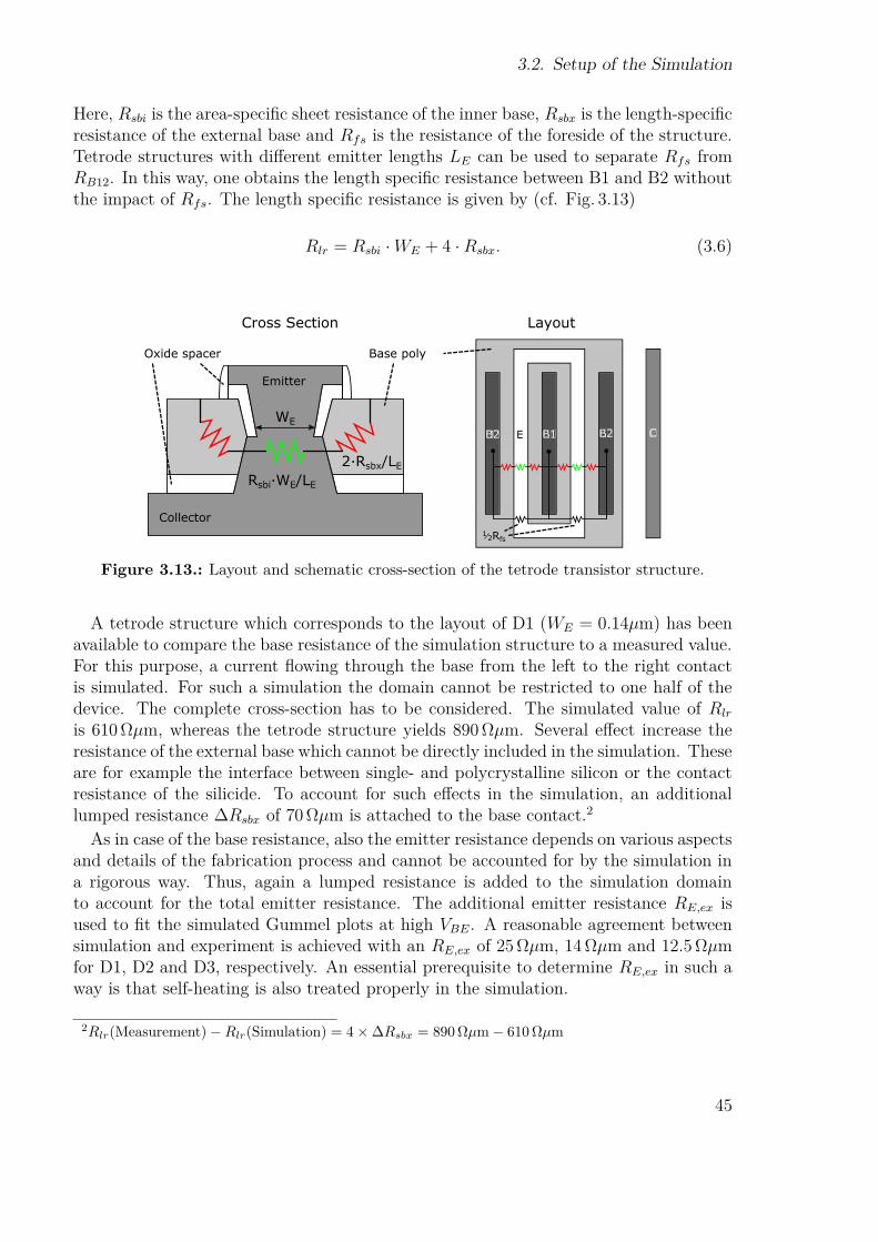
3.2. Setup of the Simulation
Here, Rsbi is the area-specific sheet resistance of the inner base, Rsbx is the length-specificresistance of the external base and Rfs is the resistance of the foreside of the structure.Tetrode structures with different emitter lengths LE can be used to separate Rfs fromRB12. In this way, one obtains the length specific resistance between B1 and B2 withoutthe impact of Rfs. The length specific resistance is given by (cf. Fig. 3.13)
Rlr = Rsbi ·WE + 4 ·Rsbx. (3.6)
Rsbi∙WE/LE
2∙Rsbx/LE
Base polyOxide spacer
Collector
Emitter
WEEB2 B1 B2 C
Cross Section Layout
Rfs12
Figure 3.13.: Layout and schematic cross-section of the tetrode transistor structure.
A tetrode structure which corresponds to the layout of D1 (WE = 0.14µm) has beenavailable to compare the base resistance of the simulation structure to a measured value.For this purpose, a current flowing through the base from the left to the right contactis simulated. For such a simulation the domain cannot be restricted to one half of thedevice. The complete cross-section has to be considered. The simulated value of Rlr
is 610 Ωµm, whereas the tetrode structure yields 890 Ωµm. Several effect increase theresistance of the external base which cannot be directly included in the simulation. Theseare for example the interface between single- and polycrystalline silicon or the contactresistance of the silicide. To account for such effects in the simulation, an additionallumped resistance ∆Rsbx of 70 Ωµm is attached to the base contact.2
As in case of the base resistance, also the emitter resistance depends on various aspectsand details of the fabrication process and cannot be accounted for by the simulation ina rigorous way. Thus, again a lumped resistance is added to the simulation domainto account for the total emitter resistance. The additional emitter resistance RE,ex isused to fit the simulated Gummel plots at high VBE. A reasonable agreement betweensimulation and experiment is achieved with an RE,ex of 25 Ωµm, 14 Ωµm and 12.5 Ωµmfor D1, D2 and D3, respectively. An essential prerequisite to determine RE,ex in such away is that self-heating is also treated properly in the simulation.
2Rlr(Measurement)−Rlr(Simulation) = 4×∆Rsbx = 890 Ωµm− 610 Ωµm
45

3. Comparison of 2D Simulation and Experiment
3.2.5. Self-HeatingThe global self-heating model [84] is used to account for an increasing lattice temperatureat high current densities. Within this model, a uniform lattice temperature TL for thecomplete simulation domain is calculated from the dissipated power Pdiss. With thecurrent Ii and the voltage Vi at contact i, the total dissipated power is given by
Pdiss =∑i
Ii · Vi (3.7)
The global lattice temperature is calculated from the following heat balance equation:
TL − T0 = Pdiss ·RTH (3.8)
Here, RTH denotes the thermal resistance and T0 is the temperature of the correspondingheat sink connected to the device. The main advantage of the global self-heating modelis that measured values of RTH can be used in the simulation, which results in the correctexcess temperature. Measured values of RTH from the reference transistors are given inTable 3.1.
Device simulation tools are also able to simulate the electrothermal behavior of thetransistor by solving the heat equation for the lattice temperature coupled to the semi-conductor equations. In principle, such simulations yield a more realistic temperaturedistribution than the global self-heating model, which assumes a uniform temperatureover the whole device [85, 86]. However, using the global self-heating model reducessimulation time, improves the convergence of the iterative solver and allows to use me-asured values of RTH . Furthermore, as pointed out by D’Alessandro et al. [87], realisticsimulations of the thermal behavior are not possible with 2D device simulation tools,because heat diffusion is an intrinsically three-dimensional process. For these reasons,the global self-heating model is the preferred method to account for self-heating in thiswork.
In Sentaurus Device, the global self-heating model is implemented as a post-processingmodel [37]. The uniform lattice temperature TL is computed by equation (3.8), afterthe coupled solution of the transport equations. Therefore, the step size of a quasi-stationary simulation must be sufficiently small to capture the dependence of TL on theapplied bias voltage correctly. Another consequence of the fact, that the temperatureis not computed self-consistently with the other variables, is that the temperature re-sponse is not considered in the small-signal ac simulation. However, at frequencies inthe GHz range, the temperature response is very small and can be neglected, as will bedemonstrated below.
To test whether the global self-heating model can be used to simulate the RF figuresof merit of the SiGe HBTs, a comparison with full electrothermal simulations is per-formed. Within these simulations, the balance equation for the lattice temperature TLis solved in addition to the energy balance equation of the electrons [37]. A thermalcontact is added at the bottom of the simulation domain assuming that most heat isdissipated to the substrate. The thermal resistance at this contact has been adjustedin such a way, that the collector current agrees with the results from the simulations
46

3.2. Setup of the Simulation
Figure 3.14.: Comparison between full electro-thermal simulation and the global self-heating model. a) fT as a function of IC . b) Collector current and maximum latticetemperature as a function of VEB. VCB = 0 V.
Figure 3.15.: Distribution of the latticetemperature TL at VBE = 0.9 V. The ma-genta line indicates the thermal contact.
Figure 3.16.: Cross-sections of TL and thesmall-signal temperature response ∆TL atx = 0.001µm for VBE = 0.9 V.
with the global self-heating model. The simulated collector current IC and the latticetemperature TL are plotted in Fig. 3.14b as a function of base-emitter voltage. In case ofthe full electrothermal simulation, the maximum value of TL is plotted, which roughlyagrees with the average junction temperature of the transistor. Both simulations agreevery well. The spatial distribution of the lattice temperature is illustrated in Fig. 3.15.The simulated transit frequency fT is plotted in Fig. 3.14a as a function of the collectorcurrent density for the different simulation approaches. It can be seen that both appro-aches yield the same fT . This result shows that the small-signal response of TL has nosignificant impact on fT .
Small-signal ac simulation computes the linear response of the device to a small sinus-oidal variation of the dc voltage. For this purpose, the system variables (n, p,Φ, Tn, TL)are written in the from ξ(t) = ξ0+ξ(ω)eiωt, with the dc solution ξ0 and the corresponding
47

3. Comparison of 2D Simulation and Experiment
small-signal response ξ [37]. The magnitude of the small-signal response of the latticetemperature |T | is plotted in Fig. 3.16 for different frequencies. A strong decrease of |T |with increasing frequency can be observed. The transit frequency is determined fromthe small-signal current gain h21 at a frequency of 40 GHz (cf. Section 3.3). At such highfrequencies, the impact of the lattice temperature response can be neglected. For thisreason, the RF figures of merit can safely be calculated from simulations that utilize theglobal self-heating model.
3.3. Calculation of fT and fmaxThe transit frequency fT is defined as the frequency at which the magnitude of thesmall-signal short-circuit current gain h21 becomes one. Correspondingly, the maximumoscillation frequency fmax is defined as the frequency where the power gain becomes one.There are different definitions for the power gain of the HBT. Here, Mason’s unilateralgain U is used to determine fmax. U can be calculated from the impedance parametersby [88]
U = |z21 − z12|2
4 [Re(z11) Re(z22)− Re(z12) Re(z21)] . (3.9)
Both h21 and U can be determined as a function of frequency using small-signal ACsimulation, as shown in Fig. 3.17a. At low frequencies, the gain is constant. At highfrequencies h21 can be approximated by (cf. Section 4.2.2)
h21 = gmjω(CEB + CBC) . (3.10)
Assuming that gm and (CEB+CBC) are independent of the frequency, |h21|2 falls off witha slope of −20 dB per decade. The same ideal slope can be derived for the unilateralgain U . The results of small-signal simulation show that this assumption is valid forh21 up to a frequency of 100 GHz. At higher frequencies, the simulated gain deviatessignificantly from the ideal slope. In contrast, the simulated unilateral gain U shows anideal behavior up to 1 THz. Note that the simulation domain does not include couplingof the collector to the substrate. Typical substrate coupling networks used in compactmodels cause U to decay with a steeper slope than −20 dB per decade.
In reality, reliable measurements of the gain at frequencies as high as fT and fmaxare not possible. Thus, fT and fmax are usually determined by an extrapolation of thegain to higher frequencies, assuming an ideal slope of −20 dB per decade. Under thisassumption, fT and fmax can simply be calculated from the gain at a single frequency:
fT = |fex · h21(fex)| (3.11)
fmax = fex ·√U(fex) (3.12)
Here, fex denotes the extrapolation frequency. Fig. 3.17b shows the extrapolated fTand fmax as a function of fex. The transit frequency fT increases significantly at higherextrapolation frequencies because the slope of the simulated h21 deviates from the ideal
48

3.4. Simulation Results
−20 dB/dec. For example, the fT value which results from an extrapolation at 40 GHzis 360 GHz, compared to 420 GHz where the simulated |h21| equals 0 dB.
Figure 3.17.: a) Calculated current gain h21 and unilateral power gain U as a function offrequency at VBE = 0.9 V. b) fT and fmax as a function of the extrapolation frequency.
Experimentally, fT and fmax are determined in this work by extrapolation of h21 andU at 40 GHz, respectively. For this reason, the simulated figures of merit which arepresented in the following are determined by (3.11) or (3.12) with fex = 40 GHz.
3.4. Simulation ResultsMeasured and simulated Gummel characteristics of D2 are shown in Figure 3.18. Due tothe adjustment of the effective bandgap and the emitter contact resistance RE,ex, a goodagreement between measured and simulated collector current is achieved. The base cur-rent is also shown in this figure. It is determined by recombination in the base and in theemitter. Ohmic boundary conditions are used at the contacts corresponding to infiniterecombination velocities. The following bulk recombination models have been activatedin Sentaurus Device: Auger recombination, Shockley-Read-Hall (SRH) recombinationwith doping dependent recombination lifetimes, the trap-assisted tunneling model bySchenk as well as the band-to-band tunneling model by Hurkx [37, 50, 89]. The de-fault model parameters have been used in the simulation. For VBE > 0.5 V, there is aquite good agreement between simulated and measured IB. At smaller VBE, where thebase current is dominated by band-to-band tunneling, the simulation deviates from themeasurement. The base current at low VBE is not relevant for a correct simulation ofthe high-frequency figures-of-merit fT and fmax, so no adjustment of the recombinationmodels has been carried out here.
The measured and simulated ideality factor of the collector current nIC is also shownin Fig. 3.18. The simulation yields a collector current that is less ideal than the measured
49

3. Comparison of 2D Simulation and Experiment
current. At VBE = 0.5 V the measured nIC is 1.025, whereas the simulated nIC is 1.033.As a result, the simulated IC at high VBE is slightly smaller than the measured currentbecause the simulated IC has been fitted to the measurements at VBE = 0.5 V. An in-depth discussion of the simulated collector current ideality is given in the Section 3.4.2.
Figure 3.18.: Measured and simulatedgummel characteristics and the ideality ofthe collector current nIC of device D2.
Figure 3.19.: Measured and simulated fTand fMAX of device D2 at VCB = 0V .
Measured and simulated fT and fmax of D2 are shown in Figure 3.19 as a functionof the collector current density. Up to a current density of about 5 mA/µm2, a goodagreement between experiment and simulation can be observed. However, the simulatedfT begins to decrease at a significantly lower current density than the measured curve. Itreaches its peak value of only 367 GHz at a current density of 10 mA/µm2 (VBE = 0.9 V),whereas the measured peak value of fT equals 404 GHz at 16 mA/µm2 (0.93 V). So, thesimulated peak fT is 9 % smaller than the real value. A similar behavior can be observedfor fmax. At low current densities, simulation and measurement match well but thefmax roll-off also starts earlier in the case of the simulation. It yields a peak fmax of208 GHz at 9 mA/µm2 compared to the measured value of 238 GHz at 12 mA/µm2. Adetailed investigation of the difference between measured and simulated fT is given inSection 3.4.4 and Section 3.4.5.
3.4.1. Hydrodynamic Transport Model ParametersThe transport model parameters r, f td and fhf have a significant impact on the simula-tion results. Following the suggestions of [59] and [10], the energy flux coefficient r andthe thermal diffusion parameter f td are set to 1. The heat flux diffusion factor has to besufficiently small to avoid an unphysical negative Early-Voltage. Simulated Gummel andoutput characteristics are shown in Fig. 3.20 for different values of fhf . For fhf > 0.5 anegative Early-Voltage can be observed in the output characteristics with a fixed VBEof 0.7 V. For values of fhf smaller 0.5, this effect does not occur. Very small valuesof fhf lead to a significant decrease of the collector current and to an increase of nIC .
50

3.4. Simulation Results
Best agreement with the measured Gummel and output characteristics is achieved forfhf = 0.4. This value is used throughout this work. The impact of fhf on the simulatedtransit frequency is shown in Fig. 3.20c. One can see that fT increases with higher valuesof fhf , except for fhf = 0.05 which yields approximately the same fT as fhf = 0.6. Themaximum value of fT ranges from 365 GHz for fhf = 0.2 to 395 GHz for fhf = 1.
In [59] and [10], the heat flux parameter has been calibrated to the results of BTEsimulations. An optimal fhf of 0.07 was obtained in [59] for a generic HBT with fT of450 GHz. A value of 0.295 was found in [10] to be suitable for different HBT generations.
Figure 3.20.: a) Simulated collector current and corresponding ideality for different values offhf . Symbols indicate measurements. b, d) Measured and simulated output characteristics.c) Measured and simulated fT .
3.4.2. Impact of the Bandgap on the Collector Current IdealityThe ideality of the collector current of a SiGe HBT is highly sensitive to the shape andthe position of the Ge profile [90]. This can be explained by the Moll-Ross relation forthe collector current which is given by (2.75). Assuming a constant electron diffusivity
51

3. Comparison of 2D Simulation and Experiment
Dn, the saturation current JC0 can be written as
JC0 = qDn
(∫ wb
0
p(x)n2i,eff (x)dx
)−1
. (3.13)
The saturation current is determined by the integral of the base charge p weighted bythe square of the effective intrinsic density ni,eff . The effective intrinsic density dependsexponentially on the bandgap (cf. (2.76)). Thus, if there are regions in the base in whichthe Ge concentration is small, these regions make a major contribution to the integralin (3.13) due to a small n2
i,eff . In case of the doping profile which is investigated here,a considerable part of the base doping lies inside the gradient of the Ge profile wherethe Ge concentration is relatively low. A change of the base-emitter voltage changes thewidth of the BE space-charge region and shifts the boundary of the neutral base. Thisshift leads to a change of the hole concentration p in the particular region where the Geconcentration is small. For this reason, the HBTs used here have a relatively high nICof about 1.02. In comparison, the HBTs with box-shaped Ge profiles used in Section 2.3have a nIC of less than 1.002.
One possibility to obtain a better agreement between measured and simulated collec-tor current ideality is to adjust the shape of the vertical Ge profile [74]. However, thisapproach does not necessarily yield a more realistic profile. At worst, one just compen-sates the insufficiency of the physical models by a wrong Ge profile. Another possibilityto fit the simulated nIC is to adjust the model of doping induced bandgap narrowing.Assessing the shape of the bandgap at the emitter side of the base in more detail, itturns out that, besides the Ge gradient, doping-induced bandgap narrowing also has astrong impact on the ideality of the collector current.
In the following, these two possible sources for the poor agreement between measuredand simulated ideality are investigated. Therefore, two examples are presented whichdemonstrate that the ideality of the simulated collector current can be matched to themeasurement. First, this matching is accomplished by an adjustment of the Ge profile.In the second example, it is accomplished by changing the doping-induced bandgapnarrowing model.
Measured and simulated Gummel characteristics and the corresponding nIC are shownin Fig. 3.21 for three different cases. Fig. 3.21a shows the results of the original simulationwith the vertical profile from Section 3.2.2 and the bandgap narrowing model describedin Section 2.3. The results of the simulations with the adjusted Ge profile and thechanged bandgap narrowing are shown in Fig. 3.21b and Fig. 3.21c, respectively. Theadjusted Ge profile is plotted in Fig. 3.22b. Compared to the original profile, the leadingedge has been shifted towards the emitter by 0.8 nm. An error of a few nanometerscan be assumed for the relative position of the measured boron and Ge profiles, so theadjusted profile still lies within the expected error range. The shift of the Ge profile leadsto a higher Ge concentration at the base-emitter junction and thus to a higher collectorcurrent. To get the same collector current with the shifted Ge profile, the Ge-dependentbandgap has to be reduced. Agreement with the measured IC is achieved for the newprofile using a ∆Eg,Ge of 6.8 meV/%. The collector current ideality is reduced by the
52

3.4. Simulation Results
Figure 3.21.: Measured and simulated Gummel plots and collector current ideality for D2.a) Simulated with original profile and bandgap. b) Simulated with shifted Ge profile. c)Simulated with uniform bandgap narrowing.
profile shift to 1.025 at VBE = 0.5 V which agrees with the measured nIC . However,the VBE dependence of nIC still differs from the measured results. A better agreementcould in principle be achieved by further adjustment of the Ge profile, but this wouldbe in contradiction with the measured profile. The effect of the profile changes can alsobe observed in the conduction band, which is shown in Fig. 3.22. The conduction bandpeak at the BE junction, which becomes significant at VBE = 0.7 V, is less pronouncedin case of the shifted Ge profile.
In the second row of Fig. 3.22 the bandgap is illustrated for the three different si-mulations. Both the SiGe bandgap Eg,SiGe and the effective bandgap Eg,eff are shown.Eg,SiGe only includes the bandgap reduction due to germanium while Eg,eff also includesthe doping-induced bandgap narrowing:
Eg,SiGe = 1.12−∆Eg,Ge (3.14)Eg,eff = 1.12−∆Eg,Ge −∆Eg,dop (3.15)
The difference between the two curves is the doping-induced bandgap narrowing ∆Eg,dop.One can see that the shape of the bandgap at the edge of the BE space-charge region isnot only determined by the Ge profile but also by the doping-induced bandgap narrowing.∆Eg,dop, which is modeled as function of the total doping concentration NA + ND, hasa local minimum at the BE junction and a maximum in the center of the base. Thiscauses the strong gradient of the bandgap which, in case of the original profile, leadsto the higher ideality factor. The shift of the Ge profile towards the emitter reducesthe impact of ∆Eg,dop on the shape of the bandgap in that region, and thus leads to areduction of nIC .
Due to the fact that doping-induced bandgap narrowing is mainly responsible for thepoor agreement between measured and simulated ideality, it is interesting to see howthe ideality behaves if the bandgap is only determined by the Ge profile. Therefore, thedoping dependence of the bandgap is switched off and a uniform bandgap narrowing is
53

3. Comparison of 2D Simulation and Experiment
Figure 3.22.: Vertical profile, bandgap and conduction band energy as a function of depth.Left column (a) shows simulations with the original profile and bandgap narrowing. Centerand right columns (b, c) show simulations with a shifted Ge profile and a uniform doping-induced bandgap narrowing, respectively.
applied to the whole device. The value of the uniform BGN equals the doping-inducedBGN in the center of the base so that the collector current density is similar in bothsimulations. The resulting bandgap is illustrated in Fig. 3.22c and the correspondingsimulation results are shown in Fig. 3.21c. A very good agreement between measuredand simulated nIC can be observed in this case.
These results show that the simulated collector current ideality is extremely sensitiveto the shape of the the band structure at the base-emitter junction, especially if theleading edge of the Ge profile is close to the leading edge of the base doping. A reaso-nable agreement between measured and simulated nIC can be achieved by a shift of theGe profile by 0.8 nm which is justifiable by the inaccuracy of the profile measurement.However, it is also possible that the bandgap peak in the BE depletion region, whichis caused by doping-induced bandgap narrowing, is overestimated in the simulation. Inthis case, the shifted Ge profile would compensate an insufficient physical model. Theimpact of the profile and bandgap changes on the simulated fT is shown in Figure 3.27.
54

3.4. Simulation Results
3.4.3. High Injection and Self-HeatingSelf-heating has a significant impact on the RF-performance of SiGe HBTs. Hence, itis important that this effect is considered properly in the simulation. In this section weexamine how accurate self-heating can be described by the global self-heating model thatuses a uniform lattice temperature for the whole device. Figure 3.23 shows the collectorcurrent as a function of VBE for different VCB illustrating the effect of self-heating.According to (3.7), the dissipated power increases with VCB leading to an increase of thelattice temperature TL at a sufficiently high current density. The higher temperature inturn leads to an increase of IC . So, the Gummel characteristics measured at differentVCB split up at high VBE due to self-heating. This effect is most pronounced for D3with WE = 0.41µm because more power is dissipated by a larger transistor. The dottedlines in Fig. 3.23 show the simulation results with the standard profile and a constantthermal resistance, the same setup that is used for the simulations in Figs. 3.18 and3.19. The dashed lines result from simulations with the Ge profile which is shifted by0.8 nm, as shown in Fig. 3.21b. The solid lines show the results of simulations whichuse a temperature-dependent thermal resistance RTH(T ) (in addition to the shifted Geprofile).
Figure 3.23.: Measured and simulated IC as well as simulated lattice temperature TL as afunction of VBE at a VCB of 0.5 V, 0 V and −0.5 V.
The standard simulation reproduces the split-up of the Gummel plots quite well forVCB of −0.5 V and 0 V. The absolute value of IC is a bit too small at such high VBE dueto the overestimation of nIC . The shifted Ge profile gives a better agreement with themeasurement. However, in the case of the strongest self-heating at VCB = 0.5 V, boththe standard simulation and the simulation with the shifted Ge profile strongly underes-timate the collector current at VBE > 0.9V. The main reason for this underestimationis the assumption of a constant thermal resistance. At lattice temperatures in excess of400 K the temperature dependence of RTH has to be taken into account. Here, RTH(T )
55

3. Comparison of 2D Simulation and Experiment
is described by the phenomenological model
RTH(T ) = RTH(300 K)(
T
300 K
)η(3.16)
with η = 0.3, which yields a reasonable increase of TL. The global self-heating modelin Sentaurus Device does not support a temperature dependent RTH . In order to stillproduce Gummel plots with temperature dependent RTH , successive simulations withstepwise increasing RTH have to be performed. The quasi-stationary ramp-up of VBEis interrupted and restarted with an updated RTH , whenever the lattice temperaturehas risen by 10 K. As a consequence of this simulation procedure, small steps can beobserved in the simulated curves in Fig. 3.23. In case of the two larger transistors D2and D3, the agreement between measurement and simulation is significantly improvedby taking into account the temperature dependence of RTH . However there is still anotable deviation at very high VBE.
In case of the smallest HBT, the impact of the temperature dependence of RTH ismuch smaller because of the lower lattice temperature TL. Furthermore, the deviationbetween measured and simulated current at very high VBE is most pronounced for D1.One probable cause of the poor agreement in case of D1 could be the non-uniformityof the SiGe base layer. The SiGe layer tends to be thicker at the edge of the collectorwindow (cf. Fig. 3.1). In connection with current crowding, this could lead to an effectivebandgap reduction at high current densities.
Figure 3.24.: Measured and simulated output characteristics at a fixed VBE of 0.7 V, 0.86 Vand 0.9 V.
Output characteristics for the three devices are shown in Fig. 3.24 for a fixed base-emitter voltage of 0.7 V, 0.86 V and 0.9 V. Simulation results are again shown for thestandard setup, for the simulation with the shifted Ge profile and for the simulation thatincludes the shifted Ge profile and the temperature dependence of RTH . As already seen
56

3.4. Simulation Results
in the Gummel plot, the original transistor profile leads to slight underestimation of IC .The overall agreement between measurement and simulation is very good. In case ofthe largest transistor, it is necessary to take into account the temperature dependenceof RTH to reproduce the measured output characteristics at VBE = 0.9 V. In summaryit can be said that the effect of self-heating on the collector current is well reproducedby the simulation, at least up to a base-emitter voltage of 0.95 V.
3.4.4. Transit FrequencyThe dependence of the transit frequency fT on the emitter width WE is illustrated inFig. 3.25, which shows measured and simulated fT for the 3 different emitter geometries.The highest fT of 404 GHz is reached for the intermediate device D2 with a width of0.28µm. At low and medium current densities, D2 and D3 nearly show the same fTwhereas D1 has a significantly smaller fT due to the larger contribution of the deviceperimeter to the parasitic capacitance. The peak value of D3 is smaller than that of D2,due to various reasons: There is an additional delay as a result of the distributed baseresistance. Self-heating is stronger in larger HBTs and the effect of RC is increased, too.Apart from the fact that the fT roll-off sets in too early, the dependence of fT on theemitter width is well captured by the simulation. For D3, simulated peak fT is 10 %smaller and for D1 it is 6 % smaller than in the measurement.
Figure 3.25.: Measured and simulated fTfor different emitter geometries. VCB = 0 V.
Figure 3.26.: Measured and simulated fTfor different VCB for D2.
The dependence of fT on the collector-base voltage VCB is shown in Figure 3.26, wherefT is plotted as a function of IC at VCB = 0.5 V, 0 V and −0.3 V. Two opposing effectsgovern the dependence of fT on the collector-base voltage. If the BC junction is reversebiased (VCB > 0) the additional electric field counteracts the widening of the base intothe collector region and thus delays the onset of the Kirk effect. On the other hand, theadditional electric field increases self-heating, which results in a degradation of fT . Forthe transistor D2 one can see in Fig. 3.26 that peak fT is merely affected by an increaseof VCB from 0 V to 0.5 V. However the roll-off of fT is shifted to a higher current density
57

3. Comparison of 2D Simulation and Experiment
for VCB = 0.5 V. If VCB equals −0.3 V, which means that the BC junction is forwardbiased, degradation of fT due to high-current effects sets in much earlier. This resultsin a significant drop of peak fT . Qualitatively, this behavior is well reproduced by thesimulation. However, again the maximum values of the simulated fT -curves are between6 % to 9 % lower than the experimental values.
Figure 3.27.: Measured and simulated fTfor D2 at VCB = 0 V.
Figure 3.28.: Measured and simulated ICas a function VBE for D2 at VCB = 0 V.
The impact of the profile and bandgap variations discussed in Section 3.4.2 on thetransit frequency is shown in Fig. 3.27 for the example of D2. The corresponding collectorcurrents are shown in Fig. 3.28. One can see that these variations have almost no impacton fT . Only the uniform bandgap leads to a slight increase of fT at high currents.Simulations including the temperature-dependent thermal resistance are also shown andthe impact on fT is also negligible.
In the following, the reason for the marked deviation between measured and simulatedfT is examined. Quasi-static transit time analysis is used to reveal the mechanism whichis responsible for the premature fT fall-off. In order to clarify how specific featuresof the hydrodynamic transport model (e.g. velocity overshoot) are responsible for thisdeviation, a comparison with drift-diffusion simulations is performed.
3.4.5. Transit Time Analysis and Comparison with Drift-DiffusionSimulation
The quasi-static transit time analysis is a convenient method for the investigation ofthe internal transistor operation. It is based on calculating the response of the chargedensity to a modulation of the applied voltage. The change of the electron charge storedin the device ∆Qn is related to a time delay τec which limits the current gain at highmodulation frequencies. Within the quasi-static approximation, the following relationbetween fT and ∆Qn can be derived [91]:
12πfT
= ∆Qn
∆IC= τec (3.17)
58

3.4. Simulation Results
The total transit time τec can be divided into several regional transit times which accountfor the delay that is caused by charge storage in the specific region of the device:
τec = τe + τeb + τb + τbc + τc (3.18)
Here, τe, τb and τc denote the emitter, base and collector transit time, respectively. Thetransit times which are related to the EB and BC depletion regions are denoted by τeband τbc. A more detailed description of the quasi-static transit time analysis and thedefinition of the regional contributions can be found in Section 4.2.
In Figure 3.29, simulated fT as well as the corresponding regional transit times areplotted as a function of IC for both hydrodynamic and drift-diffusion simulations. Theregional transit times are calculated from 1D cross sections of the quasi-static electronand hole density response ∆n and ∆p according to the definitions (4.19 – 4.23) givenin Section 4.2.1. A vertical cross section through the center of the transistor has beenused for the calculation of the transit times. In doing so, charge storage in the exter-nal transistor regions is neglected. Nevertheless, the behavior of the transistor is wellrepresented by the transit times which are calculated from the 1D cross section throughthe center of the device. This can be seen by comparing the 1D and 2D quasi-statictransit frequencies which are shown in Fig. 3.29a and Fig. 3.29b together with fT fromsmall-signal AC simulation. The quasi-static fT is calculated according to (3.17). Inthe 1D case, ∆Qn is given by the integral of the quasi-static electron density response∆n over the 1D cross section in the center of the device, whereas in the 2D case, ∆nin integrated over the complete 2D domain. The 1D quasi-static fT is higher than thecorresponding 2D result, mainly because charge storage in the external transistor isomitted. However, both curves show the same dependence of fT on IC , which demon-strates that regional transit times of the inner vertical transistor represent the behaviorof the whole device. Furthermore, it can be seen that quasi-static fT agrees well withthe results from small-signal AC simulation.
The regional transit times are shown in Fig. 3.29c and Fig. 3.29d as a function ofIC . Based on these figures, the operation of the transistor can be separated into threedifferent regimes. At low injection, the total transit time is dominated by the depletiontransit times τeb and τbc, which decrease rapidly with increasing IC . Then, there is anintermediate region around peak fT in which all transit times change comparativelylittle with increasing IC . The dominating transit times in this region are τb and τbc. Thefollowing high injection regime is characterized by a strong increase of τb, τe and τc. InFigure 3.29 the transitions between the different regimes are indicated by dotted lines.Although these transitions are gradual, the following criteria are used here to indicatethe transition points: The threshold from the low injection regime to the intermediateregime is defined as the current density at which τeb equals τb. The transition betweenintermediate and high injection regime is defined as the current density at which τbequals 80 % of the sum of the remaining transit times (τe + τeb + τbc + τc).
As expected, the drift-diffusion simulations yield a significantly smaller fT than thehydrodynamic simulations. However, the shape of the simulated fT (IC) curve corre-sponds more closely to the measurement. The difference between HD and DD simula-tions is primarily caused by the base transit time. The higher τb in the intermediate
59

3. Comparison of 2D Simulation and Experiment
Figure 3.29.: Measured and simulated fT as a function of IC are plotted in a) and b).Solid lines show fT from small-signal AC simulation whereas dashed lines show 1D and 2Dquasi-static fT . 1D fT is calculated from the quasi-static ∆n along a vertical cross sectionat the center of the transistor. In c) and d) the regional transit times are plotted as afunction of IC . Linearly scaled x-axis is used to highlight differences between measurementand simulation as well as between HD and DD.
regime is responsible for the smaller peak fT of DD simulations. Furthermore, the highinjection regime sets in earlier in case of DD simulation because the rapid increase of τbstarts at a lower current density than for HD simulation. In addition to the delayed on-set of the high injection regime, fT shows a significant reduction within the intermediateregion for HD simulations. The following numbers emphasize the different behavior ofDD and HD simulation: At the transition to the high injection regime fT is decreasedby 20 % compared to its peak value in case of DD simulation, whereas it is decreased by42 % in case of HD simulation. For a further analysis of the difference between HD andDD simulation, cross sections of internal variables are shown in Fig. 3.30 and Fig. 3.31.
Figure 3.30 shows DD simulations of the electron and hole densities (a), the quasi-static response of the electron density ∆n relative to the collector current response ∆IC(b), the electron velocity vn (c) and the conduction band energy EC (d) for the three
60

3.4. Simulation Results
different operation regimes. The three cases shown in this figure correspond to the threecolored markings in Figure 3.29b. The spatial distribution of ∆n, which is plotted inFig. 3.30b, illustrates which location in the device contributes most to the total delay.The integration of q∆n/∆IC over the whole device yields the total transit time τec. Inthe low injection regime (red lines), a high peak at the BE junction can be seen, whichis related to the change of the electron density at the BE depletion region boundary.This peak decreases with increasing IC . In the intermediate regime (green lines), thispeak has almost vanished. The transit time is now dominated by τb and τbc, which arerelated to electrons passing the base and the BC depletion region at saturation velocity.∆n in the base is higher than in the BC depletion region due to the lower saturationvelocity in SiGe. At high injection, the Kirk effect leads to a strong increase of the holedensity at the boundary of the BC depletion region. This results in a high peak in ∆n,which is related to the rapid increase of the base transit time τb.
Figure 3.30.: Internal variables from DD simulation for three different operation regimes(marked in Fig. 3.29b by colored dots). a) Net doping as well as electron and hole density.b) Quasi-static change of the electron density. c) Electron velocity. d) Conduction band andquasi-Fermi energy.
61

3. Comparison of 2D Simulation and Experiment
The corresponding results from HD simulations are shown in Figure 3.31. Similarto the case of DD simulation, ∆n shows a high peak at the BE junction in the lowinjection regime and another high peak at the BC junction in the high injection regime.Both peaks almost vanish in the intermediate regime. In contrast to the DD results, ∆nalso varies strongly at the collector side of the BC depletion region in the low injectionregime. There is a positive peak on the base-facing side of the depletion region boundaryand a negative peak on the collector-facing side. The impact of those peaks on the totaltransit time is relatively small because they compensate each other when integrating overthe device. The reason for this behavior can be understood by looking at the electrondensity n in the BC depletion region. In case of DD simulation, n is approximatelyconstant inside the space charge region with a sharp boundary to the neutral collector.In case of HD simulation, the electron density is not constant in the depletion region dueto the strong variation of the electron velocity within this region (velocity overshoot).The transition between depletion region and neutral collector is much smoother. Thechange of sign in ∆n results from a change of n at the depletion region boundary. Withincreasing injection, the boundary to the neutral collector gets flatter and reaches deeperinto the collector, which is accompanied by a relocation of electrons from the right tothe left side.
The relatively strong reduction of fT within the intermediate regime in case of HD si-mulation can be explained by a comparison of the electron velocity. Within drift-diffusiontransport, vn cannot become higher than the saturation velocity vsat. Consequently, theelectron velocity in the base and the BC depletion region does not change significantlyat the different current injection levels shown in Figure 3.30. In contrast, the hydro-dynamic transport model accounts for velocity overshoot in the BC depletion region.This is accomplished by modeling velocity saturation as a function of the carrier energy,instead of the electric field or the gradient of the quasi-Fermi potential (cf. Sect. 2.2.2).Electrons that are accelerated in the BC space charge region can achieve high velocities(> vsat) before they gain enough energy that saturation sets in. So, in HD simulation,the electron velocity in the base and the BC depletion region still depends on the shapeof the conduction band, whereas in DD simulation, it is mainly determined by the satu-ration velocity. As a result, the electron velocity in the base and the BC depletion regionchanges significantly between the different current injection levels. The reduction of theelectron velocity with increasing IC , which can be observed in Fig. 3.31c, is responsiblefor the comparatively strong degradation of fT in the intermediate regime in case of HDsimulation.
3.4.6. Impact of the Parasitics
In this section, the contributions of various device parasitics to the high frequency per-formance of the HBT are investigated. In addition, the results of device simulation arecompared to results that have been obtained by means of compact modeling.
62

3.4. Simulation Results
Figure 3.31.: Internal variables from HD simulation for three different operation regimes(marked in Fig. 3.29a by colored dots). a) Net doping as well as electron and hole density.b) Quasi-static change of the electron density. c) Electron velocity. d) Conduction band andquasi-Fermi energy.
Evaluation of the Parasitics by Means of Device Simulation
The impact of the different parasitic elements of the HBT is investigated by a stepwisereduction of the simulation structure towards a 1D transistor. Starting point is the full2D simulation which includes self-heating, the capacitance of the contact wiring andthe parasitic series resistances RE,ex and RB,ex. As described above, the capacitancesCEB,met and CBC,met and in part also the series resistances are included in the simulationby lumped elements connected to the contacts of the 2D simulation domain. The impactof these parasitic elements on the electrical characteristics is shown in Fig. 3.32 for themedium-size transistor D2.
As a first step, self-heating (SH) is omitted, which leads to an increase of maximum fTby 58 GHz. The onset of the high injection regime is shifted to a higher current density.The simulated current density at peak fT agrees much better with the measured valuewhen self-heating is omitted. However, the shape of the fT (IC) curve has not changed.
63

3. Comparison of 2D Simulation and Experiment
Figure 3.32.: Stepwise elimination of the following parasitic elements from the 2D simu-lation: Self-heating, contact capacitance, external base and emitter resistance. a) fT as afunction of IC . b) Gummel characteristics. (“w/o Cmet” coincides with “w/o RB,ex”).
Removing the capacitance of the contact wiring leads to an increase of maximum fT byanother 23 GHz. Whereas the elimination of self-heating mainly leads to an increase offT at high injection, the reduction of the parasitic capacitance also results in a higher fTat low currents. Removing the external base resistance RB,ex has no impact on fT , buta reduction of the emitter series resistance by removing RE,ex leads to a strong increaseof fT by 50 GHz. In Figure 3.33a the peak values of fT of the different 2D simulationconfigurations are summarized for all three devices D1, D2 and D3. The impact of self-heating is lowest for the smallest transistor, with an increase of fT by 8 % in comparisonto 20 % for the largest device. On the other hand, the impact of the parasitic capacitanceof the contact is most pronounced for the smallest transistor, where fT increases by 10 %compared to only 5 % for D3. The impact of the additional series resistance is similarfor all emitter geometries.
These simulation results show that fT could be increased by 30 % to 40 %, if self-heating was eliminated and if the transistor terminals were connected ideally. In thenext step, the impact of the parasitic capacitance and resistance of the transistor itselfwill be examined. For this purpose, quasi 1D simulations of the inner transistor have beenperformed. Using such a quasi 1D simulation domain eliminates all parasitic capacitanceof the device perimeter as well as the base resistance. The resistance of the collectorwell between the contact and the center of the device can also be eliminated but seriesresistance of the inner collector and the emitter are still included in the 1D domain.Figure 3.34 shows a sketch which illustrates the 2D and 1D simulation configurations.A detailed description how to simulate the inner 1D transistor with Sentaurus TCAD isgiven in Chapter 4.
Four different configurations of the 1D simulation are compared to the full 2D simu-
64

3.4. Simulation Results
Figure 3.33.: Impact of the parasitics for devices D1, D2 and D3. a) Maximum fT forthe different 2D simulation configurations shown in Fig. 3.32. b) Peak fT for the 1D/2Dsimulation configurations from Fig. 3.35.
E B C E
B
C
2D 1D
Figure 3.34: Sketch of the 2D and 1D si-mulation configuration. External parasiticsare removed stepwise. Quasi 1D domain re-presents the inner transistor, where the das-hed part accounts for the collector well.
lation in Figure 3.35 for D2. The first configuration, referred to as full 1D, includesself-heating, the additional emitter resistance RE,ex and the resistance of the collectorwell. The collector well is modeled in the 1D simulation by an extension of verticalprofile with a constant doping concentration, as indicated in Figure 3.34. The IC-VBEcharacteristic of the full 1D simulation equals the 2D case (Fig. 3.35b). Due to theabsence of the parasitic capacitance, the 1D transistor has a much higher fT than the2D transistor. Peak fT increases by 31 % to 54 % depending on the size of the device(Fig. 3.33b). If self-heating is omitted, fT increases by another 14 % to 27 %. As in the2D simulation, this increase is due to a delay of the high injection regime. In a next step,the resistance of the collector well Rc,well is eliminated by reducing the 1D domain to theinner transistor. This results in an increase of fT by about 14 %. This increase is mainlycaused by a delay of the Kirk effect, because Rc,well leads to a reduction of the voltageat the BC depletion region. If also RE,ex is removed and only the inner transistor is
65

3. Comparison of 2D Simulation and Experiment
considered, a maximum fT of 692 GHz is obtained. A comparison of the regional transittimes of the different 1D and 2D configurations is given in Section 4.2.3.
Figure 3.35.: Comparison between 1D and 2D simulation. 1D simulation is shown withand without self-heating and external emitter resistance.
Evaluation of the Parasitics by Means of Compact Modeling
Additionally, the impact of device parasitics on fT of the transistors D1, D2 and D3 hasbeen investigated in collaboration with TU Dresden using the HICUM compact model.The results of this study have been published in [76]. HICUM is a geometry scalablephysics-based compact model for bipolar transistors. Its geometry scaling capabilitiesallow to investigate modifications of the transistor configuration [92]. Furthermore,it can be used to extract 1D transistor characteristics from actual devices. A set ofscalable HICUM model parameters has been extracted from measured characteristics oftransistors D1, D2 and D3. The impact of the different external device parasitics can beexamined by successively switching them off in the compact model. The correspondingfT -characteristics are shown in Fig. 3.36 for device D2 with WE = 0.28µm.
A very good agreement between measured and simulated fT can be observed, whichdemonstrates the high modeling capabilities of HICUM. If self-heating (SH) is turnedoff in the model, fT increases by about 60 GHz. If additionally, the external contribu-tions to the base-emitter and base-collector capacitances are removed, fT increases byanother 150 GHz. A similar increase by another 180 GHz is achieved if also the externalcontributions to the emitter, base and collector resistances as well as the internal baseresistance are removed. HICUM also covers effects associated with the device perime-ter such as collector current crowding and emitter perimeter injection. For this reason,important quantities of the internal transistor such as the transfer current and the tran-sit times depend on the ratio between the area and the perimeter of the emitter [93].
66

3.5. Summary
Figure 3.36.: fT -characteristics of D2 simulated with the HICUM compact model. Externalparasitics are successively switched off.
The characteristics of a 1D transistor are thus obtained by elimination of the perimetereffects in the parameters of the internal transistor. This leads to a further increase offT by about 100 GHz (Fig. 3.36). De-embedding of the internal 1D transistor from de-vices D1, D2 and D3 by means of the HICUM compact model yields a maximum fT ofabout 900 GHz, which is significantly higher than the result of the 1D device simulation.A possible reason for this strong discrepancy might be a wrong partition between theinternal transit time and the external parasitics in the compact model as suggested in[94]. In this publication, 1D characteristics are presented which have been extractedfrom similar transistors. Due to adaptions in the compact model a significantly smaller1D transit frequency has been obtained.
3.5. SummaryIn Chapter 3, measured electrical characteristics of SiGe HBTs with an advanced ver-tical doping profile and a measured peak fT over 400 GHz have been compared to theresults of 2D device simulation. The simulations are based on results of a comprehen-sive experimental characterization of the HBTs. The vertical doping profile has beendetermined by a combination of different experimental techniques in order to achievethe best available accuracy.
A good agreement between the measured and simulated Gummel characteristics couldbe achieved by a slight adjustment of the Ge-dependent bandgap parameters, that havebeen determined in the previous chapter. Such an adjustment is necessary for tworeasons: First, even small errors in the measured Ge profile can influence the collectorcurrent noticeably. Second, as a result of process-inherent stress, the effective bandgapalso depends on the layout of metal interconnects near the device.
67

3. Comparison of 2D Simulation and Experiment
A quite good agreement between measured and simulated output characteristics couldbe achieved by adjusting the heat flux parameter fhf .
The simulated collector current ideality showed a considerable deviation from themeasurement, which is caused by a bandgap peak in the base-emitter depletion region.This peak is a result of the doping induced bandgap narrowing. A much better agreementbetween measured and simulated ideality has been achieved by replacing the dopinginduced bandgap narrowing by a uniform bandgap reduction.
The simulated transit frequency deviates significantly from the measurement. In thesimulation, fT starts to fall-off at a lower current density than in the measurement, whichresults in an underestimation of the maximum fT . The analysis of the regional transittimes suggests that electron transport through the base is not described sufficiently wellby the hydrodynamic simulation. It has been shown that the reduction of the electronvelocity in the base and the BC depletion region with increasing current density isresponsible for the premature fall-off of fT .
The impact of the parasitic resistances and capacitances has been investigated by astepwise reduction of the simulation domain. The ideal inner 1D transistor shows fT of692 GHz, which is about 90 % higher than for the full device. About 40 % of the increaseare related to the capacitance of the device perimeter and the metal contacts. 20 % arerelated to self-heating and about 15 % each are related to emitter and collector seriesresistance. This analysis shows that the advanced vertical profile of the investigateddevices still offers a significant potential for further performance improvements. It alsoshows that the reduction of device parasitics is essential to reach the highest fT values.
68

4. Impact of Vertical Profile Variationson the Transit Frequency
In this chapter, an experimental and numerical investigation of a scaled vertical transis-tor profile is given. Different variations of the vertical profile presented in Chapter 3 areexamined regarding their RF-performance. One-dimensional quasi-static transit timeanalysis is used to understand the impact of profile changes and to identify performancelimiting factors.
This chapter is organized as follows: The next section describes how quasi 1D simula-tions of HBTs are realized in Sentaurus TCAD. Then the method of quasi-static transittime analysis as well as the regional partitioning scheme are introduced in Section 4.2.After that, the different profile variations are examined, namely, the variation of theemitter-base junction width (Sect. 4.3.1), two different selectively implanted collectorsand a variation of the position of the heterojunction (Sect. 4.3.2 and Sect. 4.3.3). Ad-ditionally, a comparison of the experimental profile with a hypothetical profile fromthe SiGe HBT scaling roadmap is made is Section 4.3.4. Finally, in Section 4.4, thequestion is discussed if the discrepancy between measured and simulated fT , that hasbeen observed in the Chapter 3, could be caused by an inaccurate determination of thevertical profile. Additionally, potential improvements of fT by further optimizations ofthe vertical profile are examined.
4.1. Simulation of the inner 1D Transistor in SentaurusDevice
Sentaurus TCAD does not support one-dimensional simulation of bipolar transistors.Alternatively, a rectangular 2D simulation domain can be used to represent the vertical1D transistor. An essential prerequisite for such simulations is the appropriate definitionof the boundary conditions for the base contact. Usually, ohmic contacts are modeledby Dirichlet boundary conditions [15, 95]. This means that the carrier densities n andp, as well as the corresponding temperatures Tn and Tp are pinned to their equilibriumvalues at the contacts. The electron and hole densities are then defined by the followingconditions:
n− p−ND +NA = 0 (4.1)np− n2
i,eff = 0 (4.2)The first equation is the charge neutrality condition, the second equation is the pn-product in thermal equilibrium. The carrier temperatures at the ohmic contact are
69

4. Impact of Vertical Profile Variations on the Transit Frequency
fixed at the value of the lattice temperature TL,
Tn = Tp = TL (4.3)
The quasi-Fermi potentials of electrons and holes, ΦFn and ΦFp are set to the value ofthe applied voltage Vapp. The electrostatic potential at the boundary is then given by
Φ = Vapp + Vbi, (4.4)
with the built-in potential Vbi which is calculated from (2.46) or (2.50). In the case ofBoltzmann statistics, an analytical solution for the boundary condition exists, which isgiven by
n =
√C2 + 4n2
i,eff + C
2 , (4.5)
p =
√C2 + 4n2
i,eff − C2 , (4.6)
Φ = Vapp + kT
qasinh
(C
2ni,eff
), (4.7)
Here, C denotes the net doping C = ND −NA. When defining the simulation domain,one has to make sure that ohmic boundary conditions are satisfied at the contacts.Therefore the contacts have to be far enough away from the junctions of the transistor.The minority carrier density and the electron temperature in the intrinsic base are faraway from equilibrium, which is why ohmic boundary conditions do not apply there.Thus, in a 1D simulation of the inner transistor, the base contact cannot be modeled asan ohmic contact. The usual way to simulate the base contact in 1D simulation is to setonly the quasi-Fermi potential of holes to the value of the applied voltage. SentaurusTCAD does not allow to pin the quasi-Fermi potential in a 1D simulation in such away. However it is possible to emulate a 1D transistor by a 2D simulation domain. Asketch of this quasi 1D domain is shown in Fig. 4.1. The transistor is simply modeledby a rectangular region with two small extensions for the base contacts at both sides.Instead of using the equilibrium values n0 and p0 at the contacts, the device simulatorallows to define a recombination velocity for electrons and holes at the contact so thatn an p are defined by [37]
Jn · n = qvn(n− n0), (4.8)Jp · n = qvp(p− p0), (4.9)
where vn and vp are the electron and hole recombination velocities and n is the normalvector to the contact surface. This option can be used to model the base contact inthe quasi 1D domain by setting the electron recombination velocity to zero. Thereby,recombination of electrons at the contact is suppressed, while the quasi Fermi potentialof the holes can still be modulated by the applied voltage. However, it is not possibleto change the boundary condition for the electron temperature in such a way. So, to
70

4.2. Quasi-Static Transit Time Analysis
prevent that the electron temperature in the base is distorted by inappropriate boundaryconditions for Tn, the base contact is not directly placed at the rectangular region whichrepresents the inner transistor. Instead, small base extensions are added at both sidesand the contacts are placed at these extensions. Inside these regions, energy transport isswitched off by setting the energy flux coefficient r to zero (cf. (2.45)). In this way, theinner transistor is thermally isolated from the base contact and the fact that Tn equals300 K at the contact does not affect the electron temperature in the inner transistor.
Figure 4.1.: Sketch of the 2D domain which is used to simulate the inner transistor (LHS).The base extensions are not in scale. A part of the actual simulation grid is shown on theRHS. The doping is extended in y-direction into the base extension.
The width of the quasi 1D domain should be small compared to its length, as otherwisethe potential drop along the base becomes significant. Here, a width of 0.01µm is used.In this case the difference of the quasi Fermi potentials between the base contacts andcenter of the base can be neglected and the current transport can be regarded as one-dimensional.
4.2. Quasi-Static Transit Time AnalysisQuasi-static transit time analysis is a useful method to investigate the performance ofvertical transistor profiles. It is based on the concept of charge control which links thechange of the terminal bias voltages to the change of the internal carrier densities [96].Internally, the transistor responds to an AC input signal with a modulation of the chargewhich is stored in the device. This change of stored charge causes a time delay whichlimits the gain of the transistor at high frequencies. A measure of this delay is the transittime τec, which is defined by
τec = 12πfT
. (4.10)
A relation between τec and the charge in the transistor can be derived by the followingconsideration [97]: The small-signal current gain in common emitter configuration is
71

4. Impact of Vertical Profile Variations on the Transit Frequency
Figure 4.2: Comparison of fT from quasi-static simulation (QS) and from small-signalAC simulation.
given by
h21 = ∆IC(ω)∆IB(ω)
∣∣∣∣∣VCE=const.
. (4.11)
Here, ∆IC and ∆IB denote the change of the collector and base current respectively,that is caused by a voltage change ∆VBE. At high frequencies, one can assume that∆IB is determined solely by the modulation of holes stored in the transistor becauserecombination can be neglected at time scales of 1/ω:
∆IB = d
dt∆Qp = iω∆Qp (4.12)
Here, ∆Qp is the small-signal hole charge. The time derivative is evaluated by writing∆Qp in the form |∆Qp|eiωt. From equations (4.10)-(4.12) and the definition of thetransit frequency |h21(fT )| = 1, one obtains the desired relation between τec and thestored charge in the transistor:
τec = ∆Qp
∆IC
∣∣∣∣∣VCE=const.
(4.13)
Due to charge neutrality, ∆Qp can be replaced in (4.13) by the electron charge ∆Qn:
τec = ∆Qn
∆IC
∣∣∣∣∣VCE=const.
(4.14)
Within the quasi-static approximation, one assumes that ∆Qn and ∆IC are independentof the frequency ω. This allows one to calculate the transit time of the transistor fromsteady-state device simulation by a small change of the DC voltage. A comparison offT calculated from (4.14) in the quasi-static approximation with the results of frequencydependent small-signal AC simulation is shown in Fig. 4.2. In case of the AC simulation,fT is extrapolated from simulated h21 at a frequency of 40 GHz. One can see that thequasi-static approximation only leads to a small underestimation of peak fT . Thus itcan be regarded as a valid approximation for the investigation of the vertical profile.
72

4.2. Quasi-Static Transit Time Analysis
4.2.1. Regional Partition of the Transit Time
With the aid of device simulation it is possible to calculate the spatial distributionof the stored charge in the device. Such simulations provide detailed information onthe regional contributions to the total transit time τec [15]. In a 1D simulation, thestored charge can easily be partitioned into different regional transit time components[98, 99]. Such a charge partitioning helps to interpret simulation results and to identifyperformance limiting factors in the vertical doping profile.
Figure 4.3.: Distribution of the transit time in the 1D transistor at peak fT . a) Verticaltransistor profile and carrier densities n and p. b) Quasi-static density response (dividedby the collector current response). Inset shows the regional contributions as indicated bycolored areas. c) Accumulated transit time of electrons τacc,n and holes τacc,p.
The regional distribution of the transit time is illustrated in Figure 4.3. The totaltransit time τec can be calculated from the small-signal change of the electron density
73

4. Impact of Vertical Profile Variations on the Transit Frequency
∆n asτec = ∆Qn
∆IC= q
∆IC
∫ l
0∆n(x) dx. (4.15)
The integral runs over the whole device from the base contact at x = 0 to the collectorcontact at x = l. The equivalent relation for holes is given by
τec = ∆Qp
∆IC= q
∆IC
∫ l
0∆p(x) dx, (4.16)
with the small-signal change of the hole density ∆p. Additionally, one can define theaccumulated electron transit time τacc,n at position x by
τacc,n(x) = q
∆IC
∫ x
0∆n dx (4.17)
or, equivalently the accumulated hole transit time
τacc,p(x) = q
∆IC
∫ x
0∆p dx. (4.18)
In this work, the partitioning scheme of van den Biesen [98] is used to investigate theregional distribution of the time delay in the transistor. Within this approach the totaltransit time is divided into five contributions (τec = τe+τeb+τb+τbc+τc). The advantageof the partition scheme of van den Biesen compared to others form the literature [99] isthat only two boundaries are needed for the regional partition of the transit time. Theseboundaries, which are labeled by xeb and xbc, are defined by the intersections of ∆n and∆p as shown in Figure 4.3b. The various transit times are defined as follows:
τe = q
∆IC
∫ xeb
0∆p dx (4.19)
τeb = q
∆IC
∫ xeb
0(∆n−∆p) dx (4.20)
τb = q
∆IC
∫ xbc
xeb
∆n dx (4.21)
τbc = q
∆IC
∫ l
xcb
(∆n−∆p) dx (4.22)
τc = q
∆IC
∫ l
xbc
∆p dx (4.23)
The emitter, base and collector transit times τe, τb and τc are related to locally com-pensated minority charge in the respective region. They are also referred to as diffusioncharging times. The base-emitter and base-collector transit times τeb and τbc are de-pletion charging times, which are related to locally uncompensated charge. The spatialdistribution of ∆n and ∆p (at peak fT ) is shown in Fig. 4.3b. The integrals definingthe regional transit times (4.19)-(4.23) are indicated by colored areas. Note that thenegative ∆n is a manifestation of the extension of the BC space-charge region into thecollector [15]. This leads to a maximum of τacc,n at the position where ∆n changes sign(see Fig. 4.3c).
74

4.2. Quasi-Static Transit Time Analysis
Other methods for calculating the regional transit time contributions additionallydistinguish between mobile charge in space-charge regions (SCR) and in neutral regions(NR) [100, 101]. However, finding an unambiguous and meaningful definition of the SCRboundaries at high injection is a cumbersome task [102, 99]. Within the partition schemeof van den Biesen, the delay τeb,N due to neutral charge storage in the base-emitter SCRis included in τe and τb. Thus, the emitter delay time τe consists of τ ∗e , the delay due tominority charge storage in the neutral emitter and a portion of τeb,N . In a transparentemitter, where recombination at the contact predominates against recombination in theneutral region, τ ∗e can be estimated by [98]
τ ∗e = 1β
(devrec,h
+ d2e
2Dh
), (4.24)
where de is the distance between the emitter contact and the base-emitter SCR, Dh isthe hole diffusivity and vrec,h is the hole recombination velocity at the emitter contact.
Neutral charge storage in the base-collector depletion region, τbc,N , is included in τband τc. Similar to τe, the base transit time τb consists of the transit time of the neutralbase τ ∗b and additional contributions of τeb,N and τbc,N . Assuming a uniform base dopingand a constant Ge concentration, the neutral base transit time can be estimated by [103]
τ ∗b = w2b
2Dn
+ wbvsat
(4.25)
with the base width wb and the electron diffusivity Dn.The depletion charging times τeb and τbc are due to uncompensated charge at the
base-emitter and base-collector junction. With the corresponding depletion capacitancesCjEB and CjBC , they can be expressed as [98]
τeb = CjEBgm
(4.26)
andτbc = CjBC
gm+ xd
2vsat. (4.27)
Here, xd is the length of the base-collector depletion region and vsat is the electronsaturation velocity. The second term in (4.27) accounts for uncompensated mobile chargein base-collector SCR. Due to the high doping at the BE junction and the small size ofthe depletion region, the impact of uncompensated mobile charge in the BE depletionregion is neglected in (4.26).
4.2.2. Small-Signal Equivalent CircuitAn expression for τec can also be derived from the small-signal equivalent circuit modelshown in Figure 4.4. The small-signal current gain h21 in common-emitter configurationunder the condition of a short-circuit load is then given by [15]
h21 = icib
= gm − jωCBC1/rπ + jω(CEB + CBC) . (4.28)
75

4. Impact of Vertical Profile Variations on the Transit Frequency
It is usually assumed that gm ωCBC at frequencies of practical interest. The currentgain then simplifies to
h21 = gm1/rπ + jω(CEB + CBC) . (4.29)
Further, one assumes that the denominator of equation (4.29) is dominated by theimaginary part at high frequencies so that h21 can be approximated by
h21 = gmjω(CEB + CBC) . (4.30)
The transit frequency is defined as the frequency at which |h21| becomes unity, whichleads to
12πfT
= CEB + CBCgm
(4.31)
The capacitances CEB and CBC can be split into depletion and diffusion capacitances.The sum of the diffusion capacitances is usually expressed in terms of the forward transittime τf :
CdEB + CdBC = τfgm. (4.32)
With this definition, equation (4.31) can be expressed in the commonly used form
τec = 12πfT
= τf + CjEB + CjBCgm
, (4.33)
with the depletion capacitances CjEB and CjBC . The forward transit time can now berelated to the regional transit times defined in the previous section. By comparing (4.33)to (4.27) and (4.26) one obtains
τec = 12πfT
= τe + τb + τc + τbc,0 + CjEB + CjBCgm
, (4.34)
where τbc,0 ≈ xd/vsat is the current-independent part of τbc.
E E
B
CBC
C
CEB rπ gmvbe
Figure 4.4.: Simple high-frequency small-signal equivalent circuit of a bipolar transistor.
The forward transit time τf includes all the delay components that are independentof the current density at low and moderate current injection. By plotting (2πfT )−1 as a
76

4.2. Quasi-Static Transit Time Analysis
Figure 4.5.: Measured (2πfT )−1 as afunction of inverse transconductance. Ex-trapolation from linear region yields τf .
Figure 4.6.: Simulated transit time τec andits regional contributions as a function of in-verse gm.
function of g−1m (see Fig. 4.5), both τf and the total junction capacitance can easily be
extracted from fT -measurements. The total capacitance CjEB + CjBC is given by theslope of a linear regression line and τf is given by its y-intersection.
In Fig. 4.6 the simulated regional transit times are plotted as a function of inversetransconductance g−1
m . At low injection, the total transit time is dominated by τeb dueto the large depletion capacitance of the base-emitter junction. With increasing collectorcurrent, the depletion charging times decrease and the contributions of τe and τb becomerelevant. At high injection, both τe and τb increase rapidly leading to the strong decreaseof fT at high currents. The collector transit time τc has no significant impact on τec.
4.2.3. Comparison of 1D and 2D SimulationIn this chapter, the impact of changes of the vertical doping profile on fT is investigatedby means of 1D simulation in order to highlight their impact on the internal transittimes. These simulations are compared qualitatively with experimental results. It isimportant to know the differences between the transit times of a realistic 2D device andan idealized 1D transistor, to draw reasonable conclusions from such a comparison. Inthis section, these differences are investigated by looking at the transit times of the diffe-rent 2D and 1D simulation configurations which have been investigated in Section 3.4.6.Figure 4.7 shows the regional transit times which correspond to the transit frequenciesshown in Figure 3.35. The results from full 2D simulations including all parasitics areplotted in Fig. 4.7a and full 1D simulations are shown in Fig. 4.7b. Transit times from1D simulation, where self-heating, collector well resistance and emitter resistance aresuccessively removed, are plotted in Fig. 4.7c, Fig. 4.7d, and Fig. 4.7e, respectively. As
77

4. Impact of Vertical Profile Variations on the Transit Frequency
in Section 3.4.5, the regional transit times of the 2D simulations are calculated froma 1D cross section through the center of the transistor, so that charge storage in theexternal regions is not included.
The main differences between the transit times from full 2D and full 1D simulationare that τb and τbc are smaller and the increase of τc is delayed in the 1D case. The mainreason is that the voltage at the BC junction is slightly smaller in the center of the 2Dtransistor due to the higher effective collector resistance.
Elimination of self-heating leads to a significant shift of the high injection regime whereτb and τe increase rapidly. Furthermore, τbc is almost constant for IC > 10 mA/µm2 inthe isothermal simulation. This indicates that the increase of τbc is caused by self-heatingdue to an increase of the collector resistance with higher temperature. Removing thecollector well resistance RC,well leads to a further shift of the high injection regime andto a small reduction of τbc. If also the external emitter resistance RE,ex is removed, afurther reduction of τbc can be observed due to the higher gm.
Simulations which only account for the internal 1D transistor, as shown in Fig. 4.7e, areused in the following to investigate the impact of variations of the vertical doping profile.By using 1D simulation, one avoids that the impact of the profile change on the transittime is concealed by the influence of device parasitics. The effect of the profile change ismore pronounced in a 1D simulation which helps to interpret the experimental results.The fT characteristics in the following section have been measured and simulated at aconstant VCE of 1.25 V because this setup usually yields the highest fT . Correspondingregional transit times are shown in Fig. 4.7f. Compared to the simulations with VBC =0 V, a lower base transit time is achieved at medium and high current densities.
78

4.2. Quasi-Static Transit Time Analysis
Figure 4.7.: Regional transit times for different configurations of 1D and 2D simulation. a)Full 2D simulation with all parasitics. b) 1D simulation including self-heating, the collectorwell and RE,ex. These parasitics are successively removed in c, d and e. f) Same simulationsetup as in e but with VCE = 1.25 V instead of VCB = 0 V.
79

4. Impact of Vertical Profile Variations on the Transit Frequency
4.3. Examples of Vertical Profile VariationsIn the following the impact of various profile variations on fT is investigated both bysimulation and experiment. For this purpose, different variations of the vertical profilefrom the transistors investigated in Chapter 3 have been been fabricated. In addition tothe experimental results, 1D transit time simulation is used to elucidate how the profilevariations affect the internal transistor operation.
4.3.1. Impact of the Base-Emitter Junction WidthThree wafer splits with a variation of the emitter-base junction width have been fabrica-ted. This profile variation was obtained by changing the thickness of the undoped siliconcap layer which is deposited after the SiGe base. The wafer splits with a measured capthickness of 13.4 nm (P0), 14.9 nm (P1) and 16.4 nm (P2) show a peak fT of 416 GHz,402 GHz and 381 GHz (see Fig. 4.8b). In Figure 4.8a, the measured transit time τec isplotted as a function of inverse gm. The extrapolated transit times are 0.205 ps, 0.209 psand 0.232 ps and the corresponding capacitances which result from the slope of the cur-ves are 44 fFµm−2, 41 fFµm−2 and 37 fFµm−2, respectively. The extrapolation of τec toinfinite gm is done from the range where τec lies between 1.25 ·τminec and 2 ·τminec , with τminec
being the minimum of the transit time. As expected, a reduction of the EB-junctionwidth leads to an increase of the depletion capacitance CjEB but also to a reduction ofthe forward transit time τf . Further insight into the distribution of the total delay canbe gained by looking at the quasi-static transit time from a 1D simulation.
Figure 4.8.: a) Measured τec as a function of g−1m for profile variations with increasing cap
thickness from P0 to P2. b) fT as a function of IC . c) Collector current density as a functionof base-emitter voltage. Measurements have been performed at fixed VCE of 1.25 V.
The results of 1D simulations are shown in Figure 4.9. The different cap thicknesses aresimply modeled by a shift of the emitter doping profile. The profile with the thinnest caplayer, labeled P0, corresponds to the standard profile described in Section 3.2.2. ProfilesP1 and P2, have an emitter doping that is shifted away from the base by 1.5 nm and3 nm, respectively. The vertical profiles are shown in Fig. 4.9a along with the simulatedelectron and hole density for a current density of 12 mA/µm2 (which is close to peak
80

4.3. Examples of Vertical Profile Variations
fT ). The transit frequency calculated in quasi-static approximation is shown in Fig. 4.9band the collector current as a function of VBE is plotted in Fig. 4.9c. The correspondingregional transit times are plotted in Figure 4.10. Here, it can be seen that a shift ofthe emitter doping away from the base leads to a strong increase of τe. In the zoomedinset in Fig. 4.10, one can also see the reduction of τeb due to the reduced depletioncapacitance. Furthermore, an increase of τb can be observed for P1 and P2 which iscaused by the an increase of the neutral base width.
Figure 4.9.: 1D quasi-static simulations with different doping profiles at the EB junction.a) Doping profile as well as electron and hole density at IC = 12 mA/µm2. b) fT as afunction of IC . c) IC as a function of VBE . VCE is fixed at 1.25 V.
Increased charge storage in the emitter is the main cause for the degradation of fTwith increasing BE junction width. Maximum fT drops from 674 GHz for P0 to 569 GHzfor P2 in the 1D simulation. The reason why a shift of the emitter doping away fromthe base leads to increased minority charge storage in the emitter is that a higher VBEis needed to reach the same collector current density (see Fig. 4.9c). As a result, moreholes are injected into the emitter at the same collector current density leading to anincreased emitter transit time. Figure 4.11 shows the band structure for the different
81

4. Impact of Vertical Profile Variations on the Transit Frequency
doping profiles at a fixed base-emitter voltage of VBE = 0.91 V. In case of profile P2there is a marked barrier at the base-emitter junction. This barrier is a result of thelarger bandgap in the EB space charge region due to a reduced bandgap narrowing asdiscussed in Section 3.4.2 (see also Fig. 3.22 for the shape of the bandgap in the EBdepletion region). At low VBE the shape of the bandgap in this particular region ismasked by the high electric field. But at high VBE, the EB space charge region collapsesand reveals the shape of the band structure. This effect can be significantly reduced bya narrower EB-junction.
Figure 4.10.: Regional transit times as a function of the collector current.
The increase of τe also has a strong impact on the shape of the simulated fT charac-teristics. Due to the domination of τe at high current densities, fT drops significantlyslower in case of a wider EB junction. However this effect is much more pronounced inthe 1D simulation than in real transistor. As shown in the previous section, the Kirkeffect sets in much earlier in a real device so that the increase of τe at high IC is cove-red by a much higher τb. The measured fT characteristics do also show a less abruptdecrease of fT for profile P2, but the effect is much less pronounced.
Both simulation and experiment show that a reduction of the width of the base-emitterdepletion region leads to a higher fT because charge storage in the neutral emitter andin the EB depletion region is reduced. However, a smaller junction width also leadsto increased tunneling at low and medium injection (cf. Fig. 3.3) and to a loweringof the base-emitter breakdown voltage BVEBO which ultimately limits the maximumdoping at the junction. Measured BVEBO for P0, P1 and P2 are 1.0 V, 1.2 V and 1.6 V,respectively, where BVEBO is defined by a reverse current of IE = 9µA/µm. So eventhe device with the thinnest cap layer shows a BVEBO which is still sufficiently high formany applications.
82

4.3. Examples of Vertical Profile Variations
Figure 4.11: Band structure of the differentprofiles at VBE = 0.91 V. The y-axis is brokenfor sake of clarity.
4.3.2. Impact of the Selectively Implanted CollectorHBTs with two different collector doping profiles have been fabricated to investigate theimpact of the selectively implanted collector (SIC) on the high-frequency performance.One of these variants has a highly doped SIC which is relatively close to the base. Theother SIC-variant has a lower doping level and is further away from the base. The highlydoped SIC receives twice the implantation dose of the lightly doped SIC, resulting inan increase of the arsenic concentration from about 8× 1018 cm−3 to 1.3× 1019 cm−3.Additionally, the thickness of the silicon buffer which is deposited prior to the SiGe baselayer is decreased. This results in a narrower base-collector depletion region.
Figure 4.12.: a) Measured τec as a function of g−1m for HBTs with different SIC doping.
b) Corresponding fT (IC) curves. c) Collector current density as a function of base-emittervoltage. Measurements have been performed at fixed VCE of 1.25 V.
Measured τec-curves of both transistor variants are shown in Fig 4.12. The device withthe highly doped SIC has a maximum fT of 402 GHz (same sample as P1 in the previoussection) while the one with the lightly doped SIC shows a maximum fT of only 347 GHz.
83

4. Impact of Vertical Profile Variations on the Transit Frequency
The forward transit time τf extrapolated from the measured τec-curve is 0.209 ps forthe transistor with the highly doped SIC and 0.267 ps for the lightly doped SIC. Thecorresponding total capacitances from the slope of τec are 41 fF/µm−2 and 38 fF/µm−2.Comparing the fT characteristics in Fig 4.12b, one can see that fT degradation sets inat a significantly lower current density in the case the lightly doped SIC. A higher SICdoping shifts the onset of the Kirk effect to a higher current density, which is shown inthe following by means of simulation.
Figure 4.13.: a) Vertical doping profile and carrier densities at IC = 12 mA/µm2. b)Simulated fT as a function of IC . c) Simulated IC as a function of VBE . VCE is fixed at1.25 V.
The vertical doping profiles used in the simulation are plotted in Fig. 4.13a. CalculatedfT values resulting from quasi-static 1D simulations are shown in Fig. 4.13b. As in theexperiment, the lightly doped SIC variant has a significantly lower peak fT than theHBT with the highly doped SIC. The corresponding regional transit times are plottedin Figure 4.14 as a function of the collector current density. This plot shows that thereduction of fT is caused by an increase of τbc and τb. The higher τbc, which is constantat high injection, is related to the larger width of the base-collector space charge region.
84

4.3. Examples of Vertical Profile Variations
The increase of τb is mainly caused by an enhancement of the Kirk effect. The Kirkeffect refers to the push-out of the base into the collector at high injection, which leadsto a rapid increase of the base transit time. It is caused by mobile electrons which arepassing the base-collector region. If the charge density of these electrons exceeds thecharge in the depletion region, majority carriers from the base spread into the depletionregion. This results in a widening of the neutral base. A higher doping of the BCdepletion region suppresses this effect. From the simulated base transit time, one cansee that the Kirk effect sets in at a current density of about 35 mA/µm2 in case of thelow SIC doping, whereas for the high SIC doping, it sets in at about 80 mA/µm2.
Figure 4.14.: Regional transit times for different variants of the selectively implanted col-lector.
Despite the significant delay of the Kirk effect, the current density at which fT reachesits maximum only changed slightly in the simulation. The reason for this is that theimpact of the emitter transit time is overrepresented in the 1D simulation. In case of thehigh SIC, τe leads to a premature degradation of fT . As a consequence, 1D simulationmight underestimate the potential performance improvements of an optimized collectorprofile.
4.3.3. Impact of the Position of the HeterojunctionThe transistor characteristics are highly sensitive to the position of the heterojunctionrelative to the base-emitter depletion region. If the leading edge of the Ge profile extendsconsiderably into the emitter, neutral charge storage in the BE space charge region willdegrade fT [104]. If, on the other hand, the leading edge of the Ge profile is located insidethe neutral base, fT is degraded by a reduction of the collector current. Hence, there
85

4. Impact of Vertical Profile Variations on the Transit Frequency
is an optimum range for the position of the heterojunction relative to the base-emitterdepletion region [100].
Figure 4.15.: a) Measured τec as a function of g−1m for HBTs with different Ge profiles. b)
Corresponding fT vs. IC curves. c) Collector current density as a function of base-emittervoltage. Measurements have been performed at fixed VCE of 1.25 V.
Figure 4.15 shows measured fT values as a function of the current density as wellas the corresponding Gummel characteristics of two HBTs with different germaniumprofiles. One device has the standard profile described in Chapter 3, the other devicehas a Ge profile that extends about 3 nm further into the emitter. The doping is similarfor both HBTs. The extension of the germanium into the emitter leads to a shift ofthe fT curve to higher current densities and to a slight decrease of maximum fT . For abetter interpretation of this result, simulations of three different Ge-profiles have beenperformed. Besides the standard profile (labeled by P0) there are two variations wherethe leading edge of the germanium is shifted towards the emitter by 2 nm (P1) and 4 nm(P2), respectively (see Fig. 4.16a).
Simulated fT characteristics and Gummel plots are shown in Fig. 4.16b and 4.16c,respectively. Highest fT is achieved by P1, the profile which is shifted by 2 nm. Both thestandard profile and the profile which extends further into the emitter show a significantdegradation of fT . The shift of the Ge profile also leads to a significant change in thecollector current between P0 and P1 because the Ge percentage at the BE junction isincreased. Between P1 and P2 there is also a small increase in IC . At low currents, P0and P1 show a similar transit frequency but the roll-off of fT sets in much earlier incase of P0. For P2, the fT curve is shifted to higher current densities. At high injection,where fT drops heavily with increasing IC , P2 shows the same behavior as P1.
To identify the different delay contributions that limit fT for P0 and P2, the spatialdistribution of the quasi-static electron and hole density response is shown in Fig. 4.17aand 4.17b at a current density of 5 mA/µm2 and 50 mA/µm2, respectively. At lowcurrent, P2 shows a much lower fT than P0 and P1. This is a result of enhanced chargestorage in the base leading to a higher τb as can be seen in the inset of Fig. 4.17a. Thestrong degradation of fT at high current densities in case of P0 is due to enhanced chargestorage in emitter. This is similar to the effect of a wider BE junction discussed above.The higher VBE at a fixed current density leads to an enhanced injection of minority
86

4.3. Examples of Vertical Profile Variations
Figure 4.16.: a) Germanium profiles. b) 1D quasi-static simulation of fT (IC) for thedifferent Ge profiles. c) Corresponding simulated collector current as a function base-emittervoltage. VCE = 1.25 V.
carriers into the emitter which results in a strong increase of τe. Profile P1 representsthe optimal position of the heterojunction which minimizes both charge storage in theemitter and in the base.
The results of the 1D simulation suggest that the standard profile P0 is still conside-rably far away from the optimum and that one could gain performance improvementsby an extension of the germanium profile into the emitter. However, the experimentalresults shown in Fig. 4.15, indicate that an extended Ge profile degrades maximum fT .This discrepancy is again a result of the strong impact of τe in case of 1D simulation.A profile which minimizes charge storage in the emitter might perform better in a 1Dsimulation, but in reality, a profile which minimizes the base transit time might delivera higher fT . To demonstrate this effect, full 2D simulations including self heating havebeen performed for the Ge profiles P0, P1 and P2. The results are shown in Figure 4.18.The lateral geometry of device D2 from Chapter 3 has been used with an emitter widthof 0.28µm. In contrast to the 1D simulation, there is practically no improvement of fT
87

4. Impact of Vertical Profile Variations on the Transit Frequency
Figure 4.17.: Spatial distribution of the quasi-static electron (solid lines) and hole (dashedlines) density response at IC = 5mA/µm (a) and IC = 50mA/µm (b). The insets show theregional transit times.
from P0 to P1. They nearly show the same fT (IC)-characteristics. One the other hand,a strong reduction of fT is shown for P2.
The results so far show that enhanced charge storage in the neutral emitter can bemitigated both by a reduction of the EB junction and by an appropriate positioning ofthe heterojunction. This leads to the question if the impact of the EB junction width,that was investigated in Section 4.3.1, is still considerable if the heterojunction is alwaysat the optimum position. Corresponding simulations are shown in Fig. 4.19. Here, fTis simulated for the three different EB junction widths and the heterojunction is shiftedto the optimum position in each case. The optimum position is met by a shift of theheterojunction by −1.5 nm, −2 nm and −2.5 nm for the standard emitter, the emittershifted by 1.5 nm and the emitter shifted by 3 nm, respectively. One can see that theimpact of the EB junction width is much weaker if the the germanium profile is optimizedaccordingly. However, there is still a marked difference in maximum fT , which is mainlycaused by enhanced charge storage in the depletion region in case of a larger junctionwidth.
88

4.3. Examples of Vertical Profile Variations
Figure 4.18: Full 2D simulation offT as a function of IC for the differentGe profiles. Lateral geometry of D2from Chapter 3 has been used (WE =0.28µm). VCE = 1.25 V.
Figure 4.19: fT from 1D quasi-static simulation for different EBjunction widths (cf. Fig. 4.9c). Emit-ter is shifted by 0 nm, 1.5 nm and3 nm away from the base. Dashedlines correspond to the results fromFig. 4.9, while solid lines are simulati-ons with an optimized position of theheterojunction. VCE = 1.25 V.
4.3.4. Comparison with Profile N3 from Scaling Roadmap
In [73], a technology roadmap for SiGe HBTs based on TCAD simulation was suggested.This roadmap defines five technology nodes with an increasing targeted maximum oscil-lation frequency fmax. Starting with node N1 which represents the currently availabletechnology with a fmax of 500 GHz to node N5 with a fmax of 2 THz which is conside-red as the physical performance limit [75]. Vertical doping profiles are derived for eachnode which yield the targeted performance under certain assumptions upon the lateraldevice structure. The vertical profile of node N3, which targets a fmax value of 1 THz,represents the theoretical profile that comes closest to the present experimental profileP0. In this section, the experimental profile P0 is compared to the hypothetical profileof node N3 by 1D quasi static simulation.
The vertical doping profiles P0 and N3 are plotted in Fig. 4.20a. The emitter profileof N3 has a lightly doped region at the BE junction to reduce the base-emitter tunnelingcurrent. This results in a relatively low base-emitter junction capacitance of 9.35 fFµm−2
compared to 11.7 fFµm−2 of P0. Further, the maximum doping concentration is higherin case of N3. An experimental realization of the lightly doped emitter region is difficultdue the diffusion of dopants. The p-doping of the base is quite similar in both profiles.The base of N3 is slightly thinner and has a smaller peak concentration. The hypothetical
89

4. Impact of Vertical Profile Variations on the Transit Frequency
Figure 4.20.: Comparison of experimental profile P0 with hypothetical profile N3 from[73]. a) Vertical doping profiles. b) fT as a function of collector current density from 1Dquasi-static simulation. c) Gummel characteristics. VCE = 1.25 V.
Ge profile N3 has an extended gradient that reaches into the lightly doped emitter aswell as a higher Ge peak concentration. The collector doping of N3 differs significantlyfrom the experimental profile. It increases exponentially from about 5× 1017 cm−3 atthe BC junction to a maximum concentration of 2× 1020 cm−3 within a range of 50 nm.The selectively implanted collector of P0 has an extension of about 70 nm and the peakconcentration is reached 100 nm after the BC junction. It is hardly possible to reproducethe collector profile of N3 with the conventional process flow.
The simulated fT characteristics of profiles P0 and N3 are shown in Fig. 4.20b andthe corresponding Gummel plots are shown in Fig. 4.20c. N3 shows a higher fT thanthe experimental profile. Its maximum value is 701 GHz1 which is 4 % higher than
1In [73] a 1D peak fT of 822 GHz was obtained for N3 by device simulations based on the BTE.However, in [105], the authors show that the BTE simulator predicts abnormal fT (IC) characteristicsfor N3 due to an artificial barrier in the conduction band which is caused by the specific dopingprofile of N3.
90
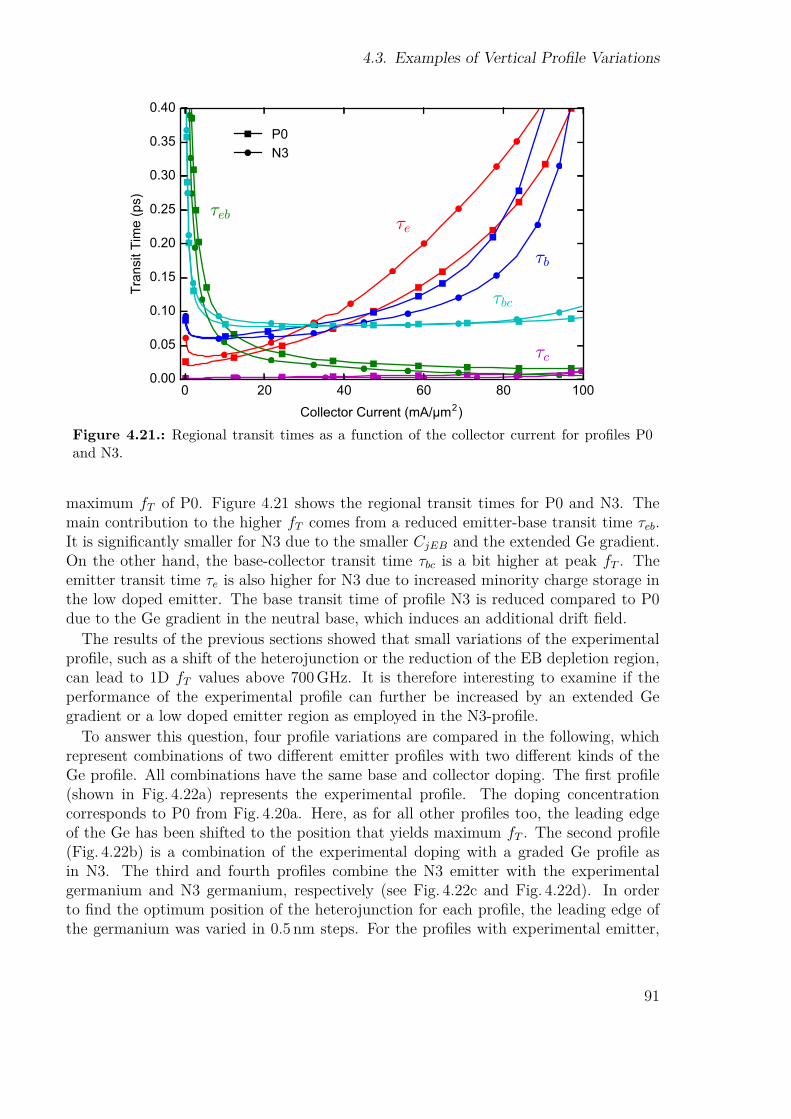
4.3. Examples of Vertical Profile Variations
Figure 4.21.: Regional transit times as a function of the collector current for profiles P0and N3.
maximum fT of P0. Figure 4.21 shows the regional transit times for P0 and N3. Themain contribution to the higher fT comes from a reduced emitter-base transit time τeb.It is significantly smaller for N3 due to the smaller CjEB and the extended Ge gradient.On the other hand, the base-collector transit time τbc is a bit higher at peak fT . Theemitter transit time τe is also higher for N3 due to increased minority charge storage inthe low doped emitter. The base transit time of profile N3 is reduced compared to P0due to the Ge gradient in the neutral base, which induces an additional drift field.
The results of the previous sections showed that small variations of the experimentalprofile, such as a shift of the heterojunction or the reduction of the EB depletion region,can lead to 1D fT values above 700 GHz. It is therefore interesting to examine if theperformance of the experimental profile can further be increased by an extended Gegradient or a low doped emitter region as employed in the N3-profile.
To answer this question, four profile variations are compared in the following, whichrepresent combinations of two different emitter profiles with two different kinds of theGe profile. All combinations have the same base and collector doping. The first profile(shown in Fig. 4.22a) represents the experimental profile. The doping concentrationcorresponds to P0 from Fig. 4.20a. Here, as for all other profiles too, the leading edgeof the Ge has been shifted to the position that yields maximum fT . The second profile(Fig. 4.22b) is a combination of the experimental doping with a graded Ge profile asin N3. The third and fourth profiles combine the N3 emitter with the experimentalgermanium and N3 germanium, respectively (see Fig. 4.22c and Fig. 4.22d). In orderto find the optimum position of the heterojunction for each profile, the leading edge ofthe germanium was varied in 0.5 nm steps. For the profiles with experimental emitter,
91

4. Impact of Vertical Profile Variations on the Transit Frequency
Figure 4.22.: Variations of the experimental profile using the emitter and Ge profile of N3.
maximum fT was achieved with a shift of −1.5 nm. In case of the N3-emitter, theexperimental Ge edge was shifted by −2 nm and the Ge edge of N3 was shifted by−1.5 nm.
Figure 4.23.: fT as a function of IC from 1D quasi static simulation. f) Gummel plot.
Simulated fT as a function of IC is shown in Fig. 4.23a and the corresponding Gummelplots are shown in Fig. 4.23b. One can see that the different emitter profiles have arelatively large impact on fT , whereas the impact of the Ge profile is smaller. Theprofiles with the N3 emitter have a higher fT at low and medium current densitiesdue to the smaller junction capacitance. However, the fT roll-off sets in earlier due toenhanced charge storage in the low-doped emitter region at high injection. The extendedGe gradient of N3 leads to a small increase of the maximum fT for both emitter variants.This effect is more pronounced in case of the N3-emitter.
92

4.3. Examples of Vertical Profile Variations
Further insight into the impact of the Ge gradient can be gained from Fig. 4.24a andFig. 4.24c where the regional transit times are compared for the different Ge profiles. InFig. 4.24a, the two variants with the experimental emitter are compared. The extendedGe gradient of N3 leads to an increase of τe, particularly at low injection. On the otherhand, it reduces τeb and τb at high current densities which results in a higher peak fT .Basically the same behavior can be observed when the Ge variants with the N3-emitterare compared (see Fig. 4.24c). The only difference is that the impact on τeb and on τb ismuch more pronounced in this case, because the extended Ge gradient reduces chargestorage in the low doped emitter region.
Figure 4.24.: Impact of the emitter and Ge profile on the regional transit times. Compa-risons of the Ge variants are shown in a) and c). Comparisons of the emitter variants areshown in b) and d).
The impact of the different emitter variants on the regional transit times is demon-strated in Fig. 4.24b and Fig. 4.24d. The lower junction capacitance of the N3-emitterresults in a reduction of τeb at low current. On the other hand, the storage of mobilecharge in the low doped emitter region leads to a strong increase of τe and τb. Compari-son of Fig. 4.24b and Fig. 4.24d shows again that the extended Ge gradient can partiallycompensate the negative effect of the low doped emitter. However this compensation islimited, even though the profiles shown here already represent the ideal position of theheterojunction.
93

4. Impact of Vertical Profile Variations on the Transit Frequency
The next question that will be examined is whether the experimental profile wouldbenefit from the collector doping suggested by N3. Therefore, simulated fT -curves withthe original collector as well as with the collector of N3 are compared in Fig. 4.25a.These simulations have been performed both with standard Ge profile and with a shiftof the leading Ge edge by −2 nm. In the both cases, maximum fT is increased by theN3 collector due to a mitigation of the Kirk effect. The impact of the collector is weakerfor the standard Ge profile, because in this case, fT is dominated by charge storage inthe emitter. Hence, a mitigation of the Kirk effect has less influence on the peak valueof fT . In the real transistor, where fT is determined by τb, one could expect a significantimpact of such a collector profile.
Figure 4.25.: Comparison of collector profiles. a) Vertical profiles. b) fT from 1D quasi-static simulation. c) Collector current as a function of VBE .
94

4.4. Sensitivity of the Simulated Transit Frequency to the Vertical Profile
4.4. Sensitivity of the Simulated Transit Frequency tothe Vertical Profile
The previous sections have shown that the transit frequency is very sensitive to certainchanges of the vertical profile. Small variations of the doping at the base-emitter junctionor the position of the heterojunction, for example, can change fT significantly. Thisraises two questions: Can the discrepancy between measured and simulated fT , thatwas found in Section 3.4, be caused by errors in the vertical profile? And to whatextend can the transit frequency of the HBTs, which are investigated here, be increasedby further optimizations of the vertical profile? In order to answer these questions, full2D simulations with the lateral geometry of device D2 and different variations of thevertical doping profile have been performed.
Figure 4.26.: a) Variations of the vertical profile. b) Measured fT (symbols) and fT from2D simulation (lines) at VCB = 0 V. c) Measured and simulated Gummel characteristics.
The first question is addressed by checking if a better agreement between measure-ment and simulation can be achieved by reasonable changes of the vertical profile. 2Dsimulations of several profile variations, which all lead to an increase of fT , are shown
95

4. Impact of Vertical Profile Variations on the Transit Frequency
in Figure 4.26. The first profile variation concerns the emitter doping. The emitterprofile (E1) is shifted towards the base by 1 nm and the maximum doping concentrationis increased from 1× 1020 cm−3 to 2× 1020 cm−3. This leads to an increase of fT , whichis mainly caused by a reduction of the emitter transit time. The higher doping concen-tration leads to a reduction of the minority carrier density in the emitter2, which reducesτe additionally to the effect of a smaller BE depletion width (cf. Section 4.3.1) and thesmaller RE. The higher doping also leads to a small reduction of the base current. Afurther enhancement of fT by shifting the Ge profile as in Section 4.3.3, could not beachieved for the profile with the optimized emitter doping. The agreement between me-asured and simulated fT in the intermediate injection regime is improved by the higheremitter doping, but the premature fT fall-off remains. Furthermore, the higher dopingleads to an increase of the junction capacitance to 14.3 fF/µm2 which disagrees withthe measured value of 11.7 fF/µm2 and leads to a reduction of fT at low injection (notvisible in Fig. 4.26b due to linear x-axis).
The next profile variation that is shown in Fig. 4.26 is a reduction of the base width(B1), which accounts for a possible error of the measured boron profile. The ion bom-bardment during SIMS leads to a relocation of the atoms at the sample surface. Thiseffect, which is known as ion-induced mixing, can lead to a broadening of the depthprofile. Thus, it might be possible that the width of the real boron profile is smallerthan the width of the measured profile. To evaluate the possible impact of such a mea-surement error, the base width (at NA = 1018 cm−3) is reduced from 11 nm to 9 nm whilekeeping the total dose constant. The green curve in Fig. 4.26b corresponds to a verticalprofile which includes both the higher emitter doping and the thinner base. One can seethat the reduction of the base width only leads to a small increase of fT . The impact ofa lower boron dose on fT has also been checked and turned out to be even smaller.
Variations of the collector profile have also been tested. Simulated fT characteristicsare shown for two variations. One includes a higher SIC doping (S1) and the otherincludes a higher doping of the collector well (C1). Both simulations also include thehigher emitter doping and the thinner base. One can see that a higher doping bothin the SIC as well as in the collector well leads to a significant increase of fT . This iscaused by a reduction of the collector resistance and a shift of the onset of the Kirk effect.However, the overall agreement between measured and simulated fT cannot be improvedby a higher collector doping. One can improve the agreement in the intermediate regime,but this leads to a strong overestimation of fT in the high injection regime. Thus, thehigher emitter doping is the only profile variation that improves the overall agreementbetween measurement and simulation. However, the higher emitter doping leads to anincrease of the BE junction capacitance which contradicts with the measured values. Inconclusion, the sensitivity analysis has shown that the deviation between measurementand simulation cannot be attributed to errors in the measured doping profile.
The profile variations of the emitter, the SIC and the collector well, (E1, S1, and C1),
2Within the depletion approximation, the minority hole density at the edge of the BE depletion regioncan be expressed as pn = n2
i
NDexp
(VBE
kT
), which illustrates the reduction of the hole injection into
the emitter with increasing donor concentration ND.
96

4.4. Sensitivity of the Simulated Transit Frequency to the Vertical Profile
are suitable candidates for a further enhancement of the transit frequency. In contrastto the emitter and the collector profile of node N3 from the scaling roadmap, they canbe realized with the conventional process flow. The reduction of the base width (B1), onthe other hand, only led to a small increase of fT , although τb strongly contributes to thetotal transit time. Therefore, a second base profile variation (B2) with a strongly reducedbase width of 5 nm (but with the same total dose) has also been tested. To fabricatesuch a thin base profile, a process with a low thermal budget would be required to reducedopant diffusion. The different base profiles are plotted in Figure 4.27.
Figure 4.27.: Base profiles with a width of11 nm (Std), 9 nm (B1) and 5 nm (B2) at adensity of 1018 cm−3. Total dose is the same.
Figure 4.28.: 2D simulation of fT as afunction of IC for different vertical dopingprofiles at VCB = 0 V.
The impact of the individual profile variations on fT is shown in Figure 4.28. Theoptimized emitter doping (E1) leads to an increase of maximum fT by 4 % (as alreadyshown in Fig. 4.26b). The reduction of the base width from 11 nm (Std) to 5 nm (B2)results in an increase of fT by 12 %. In contrast to the higher emitter doping, whichreduces fT at low injection, the thinner base leads to an enhancement at both low andmedium injection. A higher doping of the collector (by a combination of S1 and C1)leads to an increase of maximum fT by 11 %. Combining all these variations results inan enhancement of fT by 29 %.
These results show that there is still a considerable potential to increase the transitfrequency of the HBTs by further optimizing the vertical doping profile. A reduction ofthe base width and an optimized collector profile are particularly important because fTis determined by τb and τbc. A realization of the optimized emitter and collector profilesshould be possible with the current process technology. However, the realization of athin and highly doped base profile such as B2 would require a substantial reduction ofthe thermal budget.
97

4. Impact of Vertical Profile Variations on the Transit Frequency
4.5. SummaryIn Chapter 4, the impact of the vertical doping profile on the transit frequency fT hasbeen investigated by experiment and simulation. Experimental variations of the base-emitter junction width, the Ge profile and the collector doping have been compared to1D quasi-static simulations. The impact of the profile variations on fT is qualitativelywell captured by the simulation. Using regional transit-time analysis, it has been pos-sible to assign the performance changes due to profile variations to individual transittimes, which helps to identify the critical features of the vertical profile. Two importantfeatures are the width of the BE-depletion region and the position of the heterojunction.Experiment and simulation have shown that a narrow BE-depletion region helps to mi-nimize charge storage in the emitter. Further it has been shown, that the position of theheterojunction relative to the BE-depletion region has to be chosen carefully to minimizeboth charge storage in the base and in the emitter.
It should also be pointed out that an idealized 1D simulation of the intrinsic devicealone is not sufficient to optimize the vertical profile for a real transistor. The Kirkeffect is shifted to significantly higher currents in the 1D simulation. This can lead to anoverestimation of the impact of τe, because a reduction of charge storage in the emitteris much more pronounced when the Kirk effect is delayed. Thus, 1D simulation prefersprofiles which minimize τe over profiles which lead to a reduction of τb. To obtain arealistic representation of the regional transit times, self-heating as well as the emitterand collector series resistance have to be included in the simulation.
Considering these effects, the regional analysis has shown that even for such advancedvertical profiles, fT is still dominated by the transit times of the base and the BCdepletion region. To increase fT significantly in the future, it is therefore necessary torealize transistors with thin base layers and steep collector profiles as suggested in theITRS roadmap for SiGe HBTs. Here, the simulation has shown that fairly moderatechanges of the present profile can increase fT by up to 30 %.
Another important result of this chapter is that it is not possible to improve theagreement between measured and simulated fT (IC) significantly by reasonable changesof the vertical profile. This shows that the deviation, that has been found in the previouschapter, cannot be attributed to errors of experimental measurement of the verticalprofile.
98

5. Impact of Variations of the LateralArchitecture on the RF Performance
In this chapter, the influence of variations of the lateral device architecture on the RFfigures of merit is investigated. The starting point for the investigations is the devicegeometry shown in Fig. 5.1 (which is similar to the lateral geometry of IHP’s SG13G2technology [3]). The vertical doping profile from Chapter 3 is used here too. The aimof this chapter is to examine potential performance improvements from modificationsof the lateral architecture by 2D simulation. Since no quantitative comparisons withmeasurements are made, an additional resistance or capacitance at the contacts of thesimulation domain and an adjustment of the hole mobility in the external base regionas in Chapter 3 is not required here.
Figure 5.1.: Geometry of the 2D simulation domain which represents one half of the HBT.The complete domain extends to x = 1.3µm in lateral direction and to y = 2µm in verticaldirection.
This chapter is organized as follows: In Section 5.1, the impact of the width of theemitter window WE is discussed. In Section 5.2, the influence of boron diffusion fromthe external base into the inner transistor is investigated. Section 5.3 and Section 5.4deal with the impact of the collector window width WC and the oxide thickness HOx,respectively. In Section 5.5, the reference geometry shown in Fig. 5.1 is compared to thescaled geometry of the 700 GHz HBT that resulted from the DOTSEVEN project [21].
99

5. Impact of Variations of the Lateral Architecture on the RF Performance
5.1. Impact of the Width of the EmitterIn order to increase the maximum oscillation frequency fmax, a reduction of the baseresistance RB is essential, as can be seen from the well-known relation between fT andfmax which is given by [15]
fmax =√
fT8πCBCRB
. (5.1)
For a given vertical transistor profile, the base resistance can be reduced by an optimi-zation of the external base link or by a reduction of the emitter width WE. However, asmaller WE increases the relative contribution of the device perimeter to the total capa-citances and hence degrades fT . Thus, when designing the layout of an HBT there is aninevitable trade-off between maximum fT or maximum fmax. In practical applications,a balanced device design is usually desired in which fmax assumes a value between 1×fTand 2× fT .
Simulated values of maximum fT and fmax as a function ofWE are plotted in Fig. 5.2afor WE ranging from 0.03µm to 0.3µm. Simulations have been performed both withand without taking into account self-heating. For the simulations that take into accountself-heating, a linear dependence of the thermal resistance Rth on the emitter widthis assumed in accordance with the measured values of devices D1, D2 and D3 fromSection 3.1. The following relation is used to model Rth as a function WE:
Rth = 3310 KW − 1480 K
Wµm ·WE (5.2)
This assumption is obviously not valid for very wide or extremely narrow devices. Ho-wever, for the values of WE which are considered here, this should be a reasonableassumption.
Without self-heating, the HBT shows a maximum fT of 500 GHz for WE larger than0.22µm. Scaling down WE leads to a degradation of fT due to an increasing impact ofthe resistance and capacitance of the external transistor regions. On the other hand,fmax increases with decreasing WE until it reaches a maximum of almost 800 GHz atWE = 0.05µm. At this point the reduction of RB and CBC due to a smaller WE iscompensated by the degradation of fT . Taking into account self-heating leads to areduction of both fT and fmax. This effect is more pronounced for wider transistors,because the higher power dissipation of larger devices leads to a stronger self-heating,even if the thermal resistance is smaller. As a result, fT reaches its maximum at smallerWE than in the isothermal case. The peak value of 435 GHz is attained at a WE of0.2µm.
Besides fT and fmax, additional parameters are shown in Fig. 5.2 to characterize thesimulated device structures. The parameters considered here are the same that are usu-ally used to characterize the device experimentally. These are the zero-bias capacitancesCEB and CBC , the base resistance RB, the emitter resistance RE,flb and the collectorresistance RC,sat. Experimentally, the base resistance can be determined from measureds-parameters using the circle impedance method [106], which yields the sum of the base
100

5.1. Impact of the Width of the Emitter
Figure 5.2.: Influence of the emitter width on the characteristics of the HBT. a) fT andfmax. b) Sum of RB and RE extracted from s11 using the circle fit method. c) CEB and CBCat zero bias. d) RE extracted by the fly-back method and RC,sat as a function of inverse WE
and emitter resistance rb + re. The symbols in lower case indicate the results of smallsignal AC measurements. To determine the base resistance by the circle impedancemethod, the emitter resistance must be known. A common method to determine theemitter resistance is the flyback method [107], which works as follows: A current is fedinto the base while the floating voltage VCE is measured at the open collector. Theemitter resistance can then be calculated by RE,flb = ∆VCE/∆IB. RE,flb is also usedto extract the base resistance from the results of the circle impedance method, eventhough RE,flb and re are not strictly equal. Here, the base resistance RB is calculatedby RB = rb + re −RE,flb.
The collector resistance RC,sat is determined in saturation operation. At a predefinedcurrent gain β, typically between 1 and 2, the collector voltage VCE is measured. RC,sat
can then be calculated by RC,sat = ∆VCE/∆IC − (1 + 1/β)RE [107]. The emitterresistance RE must also be known to calculate RC,sat. Again, RE,flb is used for thispurpose.
CEB and CBC are plotted in Fig. 5.2c as a function of the emitter width. They showan ideal scaling behavior resulting from a constant external capacitance and an internaljunction capacitance that scales linearly with WE. RE,flb and RC,sat are plotted inFig. 5.2d as a function of the inverse emitter width. RE,flb scales nearly linear with
101

5. Impact of Variations of the Lateral Architecture on the RF Performance
W−1E . Both, RE,flb and RC,sat are determined at relatively low current densities1, hence
the influence of self-heating is weak. Fig. 5.2b shows the base resistance RB as well asrb + re, which results from the extrapolation of s11 to infinite frequency. RB shows anearly linear decrease with WE down to 0.07µm. For smaller WE, the base resistanceRB increases again. However, this increase is only an artefact of the extraction methodof RB. The emitter resistance is much larger than the base resistance at small WE. Forthis reason, the difference between re and RE,flb can become larger than rb for narrowemitters, which leads to a significant error in the extracted base resistance RB. However,such narrow emitters are not considered in the subsequent sections.
In the following, several changes of the lateral device structure are investigated. Inaddition to fT and fmax, the series resistances RE,flb, RB and RC,sat as well as thecapacitances at zero bias CEB and CBC are calculated as described above in order tocharacterize the changes of the device structure. Self-heating is not taken into accountin the following. If not stated otherwise, an emitter width of 0.12µm is used.
5.2. Base Link DopingThe doping profile at the transition from the internal base to the external base regioncannot be determined as simply and accurately as the vertical profile (which can bemeasured by SIMS with high accuracy). However, the doping profile in this region canhave a significant impact on the characteristics of the HBT.
In the SG13G2 technology, the external base region is formed by in-situ B-doped Siepitaxy after the fabrication of the emitter and after wet etching a sacrificial nitridelayer [108]. The complex fabrication of the external base region makes it difficult tomake realistic assumptions on the doping profile. It is particularly unclear how far thep-doping extends into the inner transistor. For this reason, it is important to understandthe impact of the doping at the external base link on the characteristics of the HBT, inorder to avoid that wrong assumptions on the doping profile lead to improper simulationresults.
In order to investigate the impact of the base link doping, four different profile varia-tions are compared in this section. The extension of the boron doping from the externalbase is varied in both vertical and lateral direction. Fig. 5.3a shows the 2D profile whichrepresents the maximum spreading of the external boron doping in both lateral andvertical direction. On the other hand, Fig. 5.3b shows the profile with a reduced spre-ading in both directions. One dimensional cross sections of the doping profiles alongthe lateral and vertical directions are shown in Fig. 5.3c and Fig. 5.3d. The profiles thatrepresent the stronger out-diffusion are labeled A and the profiles corresponding to lessout-diffusion are labeled B. The shape of the boron profile is not changed, it is simplyshifted by 10 nm in lateral direction and 5 nm in vertical direction. In addition to the twoprofiles shown in Fig. 5.3a and Fig. 5.3b, two mixed variants with an extended spread ofB doping in the lateral direction and a reduced spread in vertical direction and vice versa
1RE,flb is determined at IB = 2mA/µm2 and RC,sat is determined at IB = IC = 2mA/µm2
102

5.2. Base Link Doping
are also considered. The simulated electrical parameters of the four different variationsare summarized in Table 5.1.
Figure 5.3.: Doping of the base link region. a) Base link doping with strong boron out-diffusion. b) Base link doping with reduced boron out-diffusion. The solid white line is thecontour of 10 % germanium. c) Cross section of the doping profile in lateral direction aty = −0.105. d) Cross section in vertical direction at x = 0.12.
Simulated fT and fmax of the four profile variations are plotted in Figure 5.4. Acomparison of Profile 1 and Profile 2 shows a significant increase of both fT and fmaxdue to the reduced spread of p doping in vertical direction. This is accompanied by asmall reduction of CBC (see Tab. 5.1). A similar behavior can be observed by comparingprofiles 3 and 4, which, in contrast to 1 and 2, have a reduced spread of p doping inlateral direction. However, the difference in both fT and fmax is less pronounced in thiscase.
The impact of a change of the p doping in lateral direction can be seen by comparingprofiles 1 and 3 as well as 2 and 4. The reduction of boron doping under the EBspacer leads to a decrease of CEB in both cases. A small reduction of CBC can also beobserved which is more pronounced in the former case where the p doping is closer tothe collector. The base resistance increases significantly with less doping under the EBspacer. The transit frequency fT also increases with reduced spreading of the p dopingin both cases, however the difference is much larger between Profile 1 and Profile 3 thanbetween Profile 2 and Profile 4. In contrast, fmax is decreasing in both cases, but thedecrease is much stronger from Profile 2 to Profile 4.
103

5. Impact of Variations of the Lateral Architecture on the RF Performance
Table 5.1.: Simulated electrical parameters. The second and third columns contain theprofile variant in lateral and vertical direction.
No. x-Dop y-Dop fT fmax CEB CBC RB RC RElateral vertical GHz GHz fF/µm fF/µm Ωµm Ωµm Ωµm
1 A A 464 663 2.125 1.459 33.2 15.0 13.62 A B 507 730 2.125 1.428 32.5 14.9 13.73 B A 485 656 2.115 1.452 36.7 15.0 13.64 B B 509 680 2.115 1.426 37.4 14.9 13.7
Figure 5.4.: Impact of boron out-diffusion from the external base on fT (a) and fmax (b).
Overall, it can be stated that a relatively small change of the p doping at the con-junction of the internal and external base can lead to a significant change of fT andfmax. In case of Profile 1 and Profile 2 for example, a 5 nm shift of the external basedoping away from the collector leads to an increase of fT and fmax by 9 % and 10 %,respectively. In order to understand the cause of this behavior one has to examine thecharge storage in the device. Figure 5.5 shows the spatial distribution of the quasi-staticchange of the electron density ∆n for Profile 1 and Profile 4 (cf. Sect. 4.2.1 for the defini-tion of ∆n). One can see that a significant amount of charge is stored in the area wherethe SiGe layer extends into the external base region. Laterally, the SiGe base reachesup to the edge of base-collector oxide. (In fact, the silicon or SiGe that grows on theoxide is polycrystalline. In the simulation, however, it is simply modeled as crystallineSi.) In case of Profile 4 the charge storage in this area is significantly smaller than forProfile 1. The cause of this difference lies in the position of the base doping edge relativeto the SiGe layer. Cross sections of both profiles in vertical direction at x = 0.12µmare shown in Fig. 5.6, along with the conduction band energy EC , the electron densityn and the quasi-static change ∆n. Here, one can see that the enhanced charge storagein the external base region is caused by an additional barrier at the p-side of the spacecharge region between the external base and the collector. This barrier is caused bythe lower bandgap of SiGe compared to Si. The height of this barrier varies with the
104

5.2. Base Link Doping
Figure 5.5.: Quasi-static change of the electron density ∆n for the two different degrees ofboron out-diffusion shown in Fig. 5.3 at VBE = 0.9 V. a) Profile 1. b) Profile 4.
position of the space charge region relative to the SiGe layer. Ideally, the trailing edgeof the Ge profile should lie inside the space charge region so that the bandgap differenceis masked by the electric field, as it is the case in the internal base region. However,as the p-doping extends beyond the SiGe base, an additional barrier in the conductionband is formed which leads to enhanced charge storage. This is basically the same effectas the well-known formation of a parasitic barrier due to boron out-diffusion from theinternal base [109].
The occurrence of parasitic barriers in the internal base can be detected experimentallyby an unexpectedly strong dependence of IC on VCB. This method is not applicable toparasitic barriers in the external base, because the bigger part of the electrons movingfrom emitter to collector do not pass this barrier. However, it can be assumed that anincreased concentration of minority carriers in the base link region leads to enhancedrecombination, and thus to a higher base current. For this reason, it should be possible toidentify parasitic barriers in the base link region by increased neutral base recombination.
Usually, the base current is dominated by hole injection into the emitter. However,a significant contribution of neutral base recombination has been observed for someSiGe HBTs, which can lead to a degradation of the current gain and to a lower outputresistance in forced-IB operation [110, 111]. Several reasons for the observed neutral baserecombination have been discussed in the literature. In [110], an extremely low electronlifetime was assumed in the vicinity of the CB heterojunction to model the observed basecurrent, although no defects have been found by TEM investigations. In [112], it wasshown that such an enhancement of the recombination can also be caused by parasiticbarriers in the CB depletion region due to dopant outdiffusion from the SiGe base intothe Si collector. In [113], the presence of traps in the CB depletion region has beenassumed to reproduce the observed dependence of the base current on the collector-basebias.
A reduction of the base current with increasing VCB is a clear indication of neutralbase recombination. A higher reverse bias voltage at the base-collector junction leads
105

5. Impact of Variations of the Lateral Architecture on the RF Performance
Figure 5.6.: 1D plot in vertical direction at x = 0.12µm (cf. dotted lines in Fig. 5.5) toillustrate charge storage in the external base. a) Doping and Ge profile. b) Conduction bandenergy EC and electron density n. c) Quasi-static change of n.
to a spreading of the depletion region and to a reduction of the neutral base width.As the total recombination in the neutral base is proportional to its width, the basecurrent decreases with increasing VCB. Such an effect can also occur in the base linkregion, when excess minority charge due to a parasitic potential barrier leads to enhancedrecombination. A higher VCB can lead to a reduction of the barrier height, which resultsin less accumulation of minority carriers and thus in less neutral base recombination.Simulation results which demonstrate this effect are shown in Figure 5.7. Here, the basecurrent (normalized to its value at zero VCB) is plotted as a function of collector-basevoltage for the different variants of the base link doping. These simulations have beenperformed using drift-diffusion transport because hydrodynamic simulations led to anunrealistic increase of IB, even if recombination in the base was completely switched off.Both Auger and SRH recombination (with doping-dependent SRH lifetimes) has beenincluded in the drift-diffusion simulations [37]. Impact ionization is not included in thesimulation because the local models do not adequately capture the threshold of avalanchegeneration (cf. [113, 36]). The simulation shows a significant decrease of the normalizedbase current for Profile 1 which is caused by a modulation of the recombination in thebase link region. For Profile 2 and Profile 4, the dependence on VCB is considerably less
106

5.2. Base Link Doping
pronounced due to the absence of the parasitic potential barrier. For Profile 3, whichalso exhibits a parasitic barrier, the normalized base current lies between the two formercases because the barrier is further away from the internal region.
Figure 5.7.: Simulated base current as afunction of VCB. The base current is norma-lized to IB at VCB = 0 V. Impact Ionizationis omitted in the simulation.
Figure 5.8.: Measured normalized basecurrent as a function of VCB for HBTs withdifferent widths of the polysilicon emitter.VBE = 0.7 V.
In order to find experimental evidence for a parasitic potential barrier at the base-collector perimeter, transistors with different emitter layouts have been examined. Thesedevices have been fabricated in an experimental process during the DOTSEVEN project.They correspond to the wafer split D7a described in [21]. Four HBTs with differentsizes of the emitter polysilicon window have been compared with regard to neutral baserecombination. A smaller overlap between the polysilicon emitter and the external basehas the effect that the p-doping of the external base can reach further towards the innerregion of the transistor. So, if such barriers occur at all, it can be expected that theyare most pronounced in devices with a small overlap between emitter and base.
Figure 5.8 shows the measured normalized base current for the four different HBTs,which have a drawn width of the polysilicon emitter of 0.33µm, 0.37µm, 0.41µm and0.45µm, respectively. The three devices with the largest emitter poly widths show nearlythe same behavior. The slight decrease of the base current that can be observed up to acollector-base voltage of 0.45 V can be attributed to neutral base recombination (NBR).At higher VCB, the decrease of the base current is determined by impact ionization.The device with the smallest base-emitter overlap shows a significantly stronger NBR.In accordance with the simulation results shown in Fig. 5.7, this can be explained by anenhanced accumulation of minority electrons in the base link region due to a parasiticpotential barrier. However, it might also be possible that the stronger doping in thebase link region introduces additional traps, which increase neutral base recombination.So, increased NBR can be regarded as an indication of parasitic potential barriers in thebase link region but not as an evidence. Further investigations are needed to clarify thisissue.
107
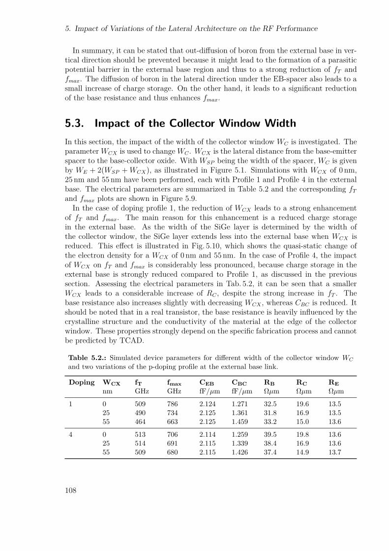
5. Impact of Variations of the Lateral Architecture on the RF Performance
In summary, it can be stated that out-diffusion of boron from the external base in ver-tical direction should be prevented because it might lead to the formation of a parasiticpotential barrier in the external base region and thus to a strong reduction of fT andfmax. The diffusion of boron in the lateral direction under the EB-spacer also leads to asmall increase of charge storage. On the other hand, it leads to a significant reductionof the base resistance and thus enhances fmax.
5.3. Impact of the Collector Window WidthIn this section, the impact of the width of the collector window WC is investigated. TheparameterWCX is used to changeWC . WCX is the lateral distance from the base-emitterspacer to the base-collector oxide. With WSP being the width of the spacer, WC is givenby WE + 2(WSP + WCX), as illustrated in Figure 5.1. Simulations with WCX of 0 nm,25 nm and 55 nm have been performed, each with Profile 1 and Profile 4 in the externalbase. The electrical parameters are summarized in Table 5.2 and the corresponding fTand fmax plots are shown in Figure 5.9.
In the case of doping profile 1, the reduction of WCX leads to a strong enhancementof fT and fmax. The main reason for this enhancement is a reduced charge storagein the external base. As the width of the SiGe layer is determined by the width ofthe collector window, the SiGe layer extends less into the external base when WCX isreduced. This effect is illustrated in Fig. 5.10, which shows the quasi-static change ofthe electron density for a WCX of 0 nm and 55 nm. In the case of Profile 4, the impactof WCX on fT and fmax is considerably less pronounced, because charge storage in theexternal base is strongly reduced compared to Profile 1, as discussed in the previoussection. Assessing the electrical parameters in Tab. 5.2, it can be seen that a smallerWCX leads to a considerable increase of RC , despite the strong increase in fT . Thebase resistance also increases slightly with decreasing WCX , whereas CBC is reduced. Itshould be noted that in a real transistor, the base resistance is heavily influenced by thecrystalline structure and the conductivity of the material at the edge of the collectorwindow. These properties strongly depend on the specific fabrication process and cannotbe predicted by TCAD.
Table 5.2.: Simulated device parameters for different width of the collector window WC
and two variations of the p-doping profile at the external base link.
Doping WCX fT fmax CEB CBC RB RC REnm GHz GHz fF/µm fF/µm Ωµm Ωµm Ωµm
1 0 509 786 2.124 1.271 32.5 19.6 13.525 490 734 2.125 1.361 31.8 16.9 13.555 464 663 2.125 1.459 33.2 15.0 13.6
4 0 513 706 2.114 1.259 39.5 19.8 13.625 514 691 2.115 1.339 38.4 16.9 13.655 509 680 2.115 1.426 37.4 14.9 13.7
108

5.3. Impact of the Collector Window Width
Figure 5.9.: Impact of the collector window width WCW on fT (a) and fmax (b) for twodifferent variants of boron diffusion from the external base.
These results show that parasitic barriers in the base link region lead to a strongdependence of fT and fmax on the width of the collector window (with respect to theemitter window). If a variation of the collector window geometry results in an unex-pectedly strong change of the high-frequency performance of the HBT, one can assumethat this device suffers from degradation due to boron out-diffusion from the externalbase. On the other hand, if fT is not affected significantly, the presence of parasiticbarriers is unlikely. In the data that has been available for this work, such a significantdependence on the collector window width has not been observed. However, no datawas available from HBTs with the smallest overlap of the emitter polysilicon and theexternal base, in which such barriers most likely occur. A comparison of devices withdifferent collector window geometries at smallest possible overlap the emitter polysiliconand the external base is still to be made.
Figure 5.10.: Quasi-static change of the electron density ∆n at VBE = 0.9 V for WCX =0 nm (a) and WCX = 55 nm (b), each with doping profile 4.
109

5. Impact of Variations of the Lateral Architecture on the RF Performance
5.4. Impact of the Oxide ThicknessIn Section 4.3.4 it was shown that an advanced vertical collector profile, as suggested in[73], can increase fT by a reduction of the Kirk effect. However, such a steep collectorprofile cannot be realized with the standard device architecture of SG13G2 because thevertical collector profile is determined by the fabrication process flow, and in particularby the thickness of the base-collector oxide. The relevant part of the process flow startswith the formation of the collector well by ion implantation, followed by the depositionof the oxide. Then the collector window is opened and filled by selective Si epitaxy.After that, the SIC is formed by a masked ion implantation, followed by the SiGe baseepitaxy. Hence, the vertical distance between the collector well and the base is definedby the oxide thickness. Reducing the thickness of the oxide thus allows to produce asteeper collector profile.
In this section the impact of a reduced oxide thickness on the RF performance of theHBT is investigated. A comparison of the doping profile of the standard device with anoxide thickness of 80 nm and the profile of a device with a reduced thickness of 40 nmis shown in Fig. 5.11. It is assumed that the same SIC implantation is used for bothversions of the oxide. The new vertical profile that results from the shift of emitter, baseand SIC towards the collector well is shown in Fig. 5.11c.
Figure 5.11.: 2D doping profile for an oxide thickness of 80 nm (a) and 40 nm (b). Thedoping profiles in vertical direction at x = 0.04µm are plotted in (c).
Simulated fT and fmax curves of the devices with a HOX of 40 nm and 80 nm are
110

5.4. Impact of the Oxide Thickness
shown in Fig. 5.12. Again, the simulations have been performed both with Version 1and Version 4 of the external p-doping. The corresponding electrical parameters aregiven in Table 5.3. The reduction of the oxide thickness leads to a significant increaseof fT at high current densities. At low and medium currents, fT becomes smaller witha thinner HOX . RC and also RE are reduced by a reduction of HOX . The reduction ofRE, however, is an artefact of the determination by the flyback method which assumesa constant reverse current gain [107]. The emitter itself is not affected by a thinneroxide, so the true RE should not be affected either. The strong reduction of RB is alsonot real. The circle impedance method assumes a negligible external BC capacitanceCBCX . CBCX and RC form a capacitive path between the base and collector terminalswhich reduces the input resistance at high frequencies. Thus the resulting RB decreaseswith increasing CBCX [107]. The base-collector capacitance CBC increases significantlywhen the oxide becomes thinner and the distance between collector and base shrinks.The increased capacitance is the reason for the lower fT at low and medium currentdensities. The reason for the strong enhancement of fT at high IC is that the onset ofthe Kirk effect is delayed due to the higher p-doping at the base-collector junction. Incontrast to fT , the peak value of fmax decreases with a thinner oxide. At low currents,fmax is significantly smaller due to the high CBC . Its peak value is shifted to higher ICdue to the suppression of the Kirk effect. However, the increase in fT is not sufficient tocompensate for the increase of CBC .
Figure 5.12.: Impact of the oxide thickness HOX on fT (a) and fmax (b) for two differentvariants of boron diffusion from the external base and WCX = 55 nm.
A comparison of the solid and dashed lines in Fig. 5.12 shows, that the doping of theexternal base has only a small effect on the impact of the oxide thickness. The increaseof peak fT is slightly higher in case of Profile 1, but mainly, the changes between 40 nmand 80 nm oxide are similar for Profile 1 and Profile 4.
Furthermore, simulations with a collector window width of WCX = 0 are shown inFig. 5.13. Here, the impact of the oxide thickness on fT and fmax is basically the same asfor WCX = 55 nm, even though one could expect a smaller impact due to the reductionof the external base-collector resistance. The fact that neither the external base doping,
111

5. Impact of Variations of the Lateral Architecture on the RF Performance
Figure 5.13.: Impact of the oxide thickness HOx on fT (a) and fmax (b) for two differentvariants of boron diffusion from the external base with WCX = 0 nm.
nor the width of the collector window influence the impact of the oxide thickness on fTand fmax, leads to the conclusion that these changes are mainly determined by the Kirkeffect and the internal base-collector capacitance.
Table 5.3.: Simulated Device Parameters
WCX Dop HOx fT fmax CEB CBC RB RC REnm nm GHz GHz fF/µm fF/µm Ωµm Ωµm Ωµm
55 1 80 464 663 2.125 1.459 33.2 15.0 13.640 501 650 2.122 2.226 29.6 12.5 12.9
4 80 509 680 2.115 1.426 37.4 14.9 13.740 530 652 2.111 2.173 34.3 12.7 13.0
0 1 80 509 786 2.124 1.271 32.5 19.6 13.540 532 771 2.121 1.795 30.9 15.4 12.4
4 80 513 706 2.114 1.259 39.5 19.8 13.640 536 693 2.110 1.772 36.9 15.8 12.5
Scaling of the vertical doping profile usually results in a trade-off between performanceand breakdown voltage. A higher doping of the collector can lead to a higher electric fieldacross the BC junction which might decrease the breakdown voltage. In order to assesif a degradation of the BC breakdown voltage has to be expected for the thinner oxide,simulations of output characteristics in common-base and common-emitter configurationhave been performed. For this purpose, the following recombination models have beenactivated in Sentaurus Device: Auger recombination, Shockley-Read-Hall recombinationwith doping-dependent lifetimes and avalanche generation with the impact-ionizationmodel from [114] (referred to as New University of Bologna Model).
Simulated output characteristics in common-base configuration for fixed IE are shown
112

5.5. Analysis of Lateral Scaling of the DOTSEVEN HBT
in Figure 5.14. The simulations predict that for VCB above 4 V, avalanche generationbecomes significant and leads to a strong increase of IC . This result is in accordancewith the measured BVCBO of 4 V for this doping profile (see Tab. 3.1). The current dueto impact ionization is also plotted in Fig. 5.14 (dashed lines). Comparing the simulatedoutput characteristics of the different oxide thicknesses shows that there is practicallyno impact on the breakdown voltage in common-base configuration.
Figure 5.14.: Output characteristics incommon-base configuration with fixed emit-ter current. Dashed lines show the currentdue to impact-ionization (II).
Figure 5.15.: Absolute value of the basecurrent as a function of VCE for fixed VBEof 0.7 V. BVCEO is defined by the change insign of IB.
The breakdown voltage in common-emitter configuration BVCEO can be determinedfrom the base current reversal with increasing VCE [115]. When avalanche generationsets in, holes which are created in the BC depletion region cancel out the forward basecurrent, which leads to a reversal of the terminal base current. Figure 5.15 shows theabsolute value of the simulated base current at VBE = 0.7 V as a function of VCE. Thebase current becomes zero at about 1.8 V for both variations of the oxide thickness.This suggests, that the proposed variation of the collector profile does not lead to adegradation of the breakdown voltage.
5.5. Analysis of Lateral Scaling of the DOTSEVEN HBTAs a result of the DOTSEVEN (D7) project, a new generation of SiGe HBTs has beendeveloped, which shows a maximum fT/fmax of 505 GHz/720 GHz. The main techno-logical measures which have led to such a strong enhancement of the high-frequencyperformance compared to the previous transistor generation are an optimized verticalprofile, a decrease of base and emitter resistance due to the application of millisecondannealing in combination with a low temperature back-end as well as lateral devicescaling. A summary of the technological progress can be found in [21].
113

5. Impact of Variations of the Lateral Architecture on the RF Performance
Scaling of the lateral device dimensions has significantly contributed to achieve fmaxof more than 0.7 THz. Its impact is demonstrated in [21] by a comparison of wafer splitswith the reference device architecture of SG13G2 and the scaled device architectureof the D7 transistor. However, these wafer splits also include process optimizationswhich lead to changes of the vertical doping profile and the conductivity of the externalbase regions. For this reason, it is difficult to estimate the impact of the scaled devicedimensions independently of the doping profile from the experimental results only.
In this section, device simulation is used to get a more detailed understanding of howscaling of the lateral device dimensions contributed to the performance enhancement ofthe new HBT generation. Therefore, simulations of a HBT with the lateral geometry ofthe reference technology (G2) are compared to simulations of the optimized geometry(D7). The same doping profile is used for all simulations, so that the differences in theelectrical characteristics are only determined by the device geometry. The doping profilewith minimal extension of the external p-doping (No. 4 in Tab. 5.1) is used for all devicemodifications.
Figure 5.16.: Simulated device structures. a) Reference structure with G2-like geometry.b) Scaled structure with the lateral geometry of the D7 HBT.
Figure 5.16 shows the 2D device structures that are used in the simulation to representthe reference and the scaled HBT design. Several intermediate stages of the devicescaling are simulated to determine their individual impact on the transistor performance.Starting with G2, the scaled D7 device is obtained by a stepwise application of thefollowing modifications:
1. The width of the emitter window WE was reduced from 0.12µm to 0.1µm.
2. The thickness of the emitter has been reduced by 50 nm.
3. The thickness of the base-emitter spacer has been reduced.
4. The silicide thickness has been increased from 20 nm to 40 nm.
5. The width of the base poly WBPLY has been reduced by 0.1µm.
114

5.5. Analysis of Lateral Scaling of the DOTSEVEN HBT
Simulated fT and fmax of the subsequent device modifications are plotted in Fig. 5.17.The corresponding electrical parameters are summarized in Table 5.4. The reduction ofWE from 0.12µm to 0.1µm results in a small reduction of fT from 523 GHz to 512 GHzdue to the stronger impact of the capacitance from the device perimeter. At the sametime, fmax increases by 11 % from 693 GHz to 766 GHz due to a reduction of the baseresistance. This behavior has already been discussed in Section 5.1. The next modifi-cation is the reduction of the emitter thickness HE, which results in a decrease of theemitter resistance. The smaller RE leads to a slight increase of fT . A greater impactis achieved by the reduction of the width of the EB-spacer. The width of the oxidebetween emitter and external base is reduced from 22 nm to 15 nm and the width of thenitride is reduced from 50 nm to 35 nm. Additionally the width of the emitter poly isreduced by 10 nm. The optimized spacer leads to a significant reduction of RB whichresults in an increase of fmax by 10 % from 766 GHz to 843 GHz. The transit frequency,however, decreases a bit due to a higher CEB. Increasing the thickness of the silicideleads to a small increase of fmax. A scaled base poly width results in to a reduction ofthe base-collector capacitance from which both fT and fmax benefit.
Figure 5.17.: a) Transit frequency vs. collector current density. b) Maximum oscillationfrequency vs. collector current density.
Table 5.4.: Simulated device darameters for various modifications of the HBT structure.
# Modification fT fmax CEB CBC RB RC REGHz GHz fF/µm fF/µm Ωµm Ωµm Ωµm
Reference 523 693 2.112 1.314 38.1 13.2 13.21 WE reduced 512 766 1.875 1.211 34.7 14.0 15.82 HE reduced 515 766 1.879 1.212 38.2 14.0 13.43 Thinner Spacer 513 843 1.938 1.180 32.7 14.4 13.44 Thicker Silicide 512 854 1.939 1.180 33.1 14.4 12.75 WBPLY reduced 517 859 1.939 1.137 33.7 13.6 12.6
115

5. Impact of Variations of the Lateral Architecture on the RF Performance
Summarizing the results above, both scaling of the emitter window and the EB spacerwidth contribute significantly to the strong increase in fmax of the D7 HBT comparedto the G2 HBT. However, these modifications also lead to a degradation of fT which hasto be compensated by an optimized vertical profile. A reduction of the base poly widthis beneficial for both fT and fmax.
The wafer split D7a presented in [21] contains modifications 1 to 4 from Table 5.4as well as additional process changes which alter the vertical profile and increase theconductivity of the external base region. Compared to a standard SG13G2 wafer, thesechanges lead to an increase of fT by 7 % from 314 GHz to 337 GHz and to an increase offmax by 43 % from 414 GHz to 591 GHz. The simulation yields a decrease of fT by 2 %and an increase of fmax by 23 % if modifications 1 to 4 are applied. The absolute valuesof the simulation results are significantly higher than the measured values because amore advanced vertical profile is used and because self heating is omitted. Comparingthe relative changes from simulation and experiment leads to the conclusion that roughlyhalf of the fmax enhancement can be attributed to the scaled lateral dimensions. Theother half can be attributed to the additional process changes, namely the higher emitterdoping, the reduced temperature of the final RTP which reduces broadening of the basedoping, the enhanced conductivity in the external base and the SIC implantation trougha hard mask instead of a resist mask which helps to reduce CBCx.
5.6. SummaryIn Chapter 5, several possible modifications of the lateral structure of the SiGe HBThave been investigated by means of simulation, regarding their impact on fT and fmax.The simulation has shown, that a reduction of the collector window width as well as athinner oxide between collector well and external base can improve the RF-performance.
The simulations have shown that out-diffusion of boron can lead to parasitic barriersin the transitional region between internal and external base. Such barriers lead to astrong degradation of fT and fmax. This effect is similar to the well known effect ofparasitic barriers in the internal base [109]. The difference is, that it is not caused byboron out-diffusion from the internal base doping but from diffusion of boron from theexternal base into the inner transistor. However, further experimental investigations arenecessary to clarify if this effect plays a role in real transistors.
Furthermore, the comparison between the lateral geometry of the DOTSEVEN HBTand the reference geometry of SG13G2 has shown that geometry scaling alone leads toan increase of fmax by almost 25 %.
116

6. Conclusions and OutlookThe primary objective of this thesis is to evaluate the ability of state-of-the-art hydro-dynamic simulation to predict the RF-performance of advanced SiGe HBTs. For thispurpose, measured and simulated DC characteristics and RF figures of merit from SiGeHBTs with a vertical doping profile tailored for high transit frequencies have been com-pared. In addition, the simulations provided valuable insight on performance-limitingmechanisms in the HBTs.
The commercial TCAD tool Sentaurus Device has been used for the hydrodynamicsimulations. Calibrated parameter models, which were developed by Sasso et al. duringthe DOTFIVE project, are applied in this work. The effective bandgap in the SiGeC baselayer has been determined experimentally for different Ge mole fractions. The obtainedbandgaps are in good agreement with published data extracted from SiGe HBTs. Nosignificant impact of carbon on the effective bandgap was found for concentrations upto 1.5× 1020 cm−3. Thus, the literature values for the effective bandgap in SiGe HBTscan also be used to simulate SiGeC HBTs with typical carbon concentrations of about1020 cm−3.
For a meaningful comparison between measurement and simulation, it is necessarythat the doping profile and the device geometry, which define the simulation domain,closely correspond with the real device. Based on a comprehensive experimental charac-terization, a simulation structure has been created which comprises all relevant featuresof the reference transistors. Long devices have been used for this comparison, so thatcharge transport can be described sufficiently accurate by a 2D simulation domain. Theprecise knowledge of the vertical doping profile is particularly important to assess thepredictive power of the simulation. Here, the vertical profile has been determined by acombination of different experimental techniques in order to achieve the best availableaccuracy.
A good agreement between measured and simulated Gummel and output characteris-tics has been achieved by an adjustment of the bandgap and the heat flux parameterfhf . However, the simulated collector current ideality showed a considerable deviationfrom the measurement. It turned out that this deviation is related to the doping-inducedbandgap narrowing model, which produces a bandgap peak in the base-emitter depletionregion. Future work should address the question if a better agreement can be achievedby an improved bandgap narrowing model. A model which takes into account the de-pendence of the effective bandgap narrowing on the carrier density (as in [116]) mightproduce a more realistic bandgap in the depletion regions.
The comparison of experimental profile variations with simulation has shown that theimpact of these variations on fT is qualitatively well captured by the simulation. Thisimplies that hydrodynamic device simulation is a useful tool for the optimization of the
117

6. Conclusions and Outlook
vertical doping profile.However, it was found that the dependence of fT on the collector current IC is not
reproduced properly by the simulation. The degradation of fT sets in at lower currentsthan in the experiment. Additionally, the transition to the high injection regime, wherethe Kirk effect leads to a rapid decrease of fT , is less abrupt in the simulation. Overall,this results in an underestimation of the maximum fT by about 10 %.
The quasi-static transit time analysis has been used to examine the impact of theprofile variations on fT . It revealed that a narrow BE depletion region leads to a higherfT by reducing minority charge storage in the emitter and that the optimum positionof the heterojunction (relative to the BE depletion region) is determined by a trade-offbetween charge storage in the emitter and in the base. Moreover, it was shown that evenfor such advanced vertical profiles, maximum fT is still dominated by the transit timesof the base and the base-collector depletion region. A significant improvement of fT canthus be expected by further scaling of the base width and the BC junction doping. Thesimulation suggests that moderate changes of the vertical profile can increase fT of thepresent HBTs by about 30 %.
Considerable improvements can also be expected from a reduction of device parasiticssuch as the series resistance of the emitter and the collector. The simulated transitfrequency of the inner 1D transistor is about 90 % higher than fT of the full device. Thisshows that the present vertical doping profile offers a significant potential for furtherperformance improvements.
Possible modifications of the lateral device architecture have been investigated bysimulation. A strong effect of the external base doping on fT was found: Enhanced boronout-diffusion from the external base link can create parasitic barriers in the conductionband, which lead to enhanced charge storage in the base link region. Such barrierswould have a particularly strong impact on laterally scaled transistors where the relativecontribution of the device perimeter to the total charge storage increases. However,further experimental investigations are needed to figure out if this effect is relevant inreal HBTs.
The comprehensive comparison between measured and simulated electrical characte-ristics presented in this thesis reveals weaknesses in the hydrodynamic simulation ofadvanced SiGe HBTs. The measured fT (IC) characteristics could not be reproducedproperly by the simulation. This suggests that the hydrodynamic transport model isnot sufficiently accurate for a reliable quantitative prediction of the high-frequency per-formance of the next generation of SiGe HBTs. In future work, it should be investigatedif simulations based on BTE are capable to reproduce the measured fT characteristics.Furthermore, it should be assessed if a more realistic model of the effective bandgapnarrowing improves the accuracy of the simulation. Nevertheless, the HD simulationswere able to qualitatively reproduce the impact of changes of the vertical profile andvariations of the lateral device geometry. Therefore, HD simulation continues to be auseful tool for the investigation and optimization of modern SiGe HBTs.
118

A. Numerical Parameters of thePhysical Models
A.1. Parameter Values of the Energy Relaxation TimeModel
Table A.1.: Parameter values are taken from [8].
Parameter Unit Value Parameter Unit Value
τw,0,Si ps 0.391 C1,Si0.7Ge0.3 1 0.0028τw,0,Si0.7Ge0.3 ps 0.449 Cc 1 -0.001818Cτ ps -0.05 C0 1 0τw,1 ps -0.14434 C2 1 -0.059C1,Si 1 0.00135 C3 1 0.0107
A.2. Parameter Values of the Mobility Model
Table A.2.: Parameters for Si taken from [8]. Normalized temperature Tn = T/300K.
Parameter Unit Electrons Holes
µmax,0 cm2/Vs 1421.6 485.51γ -2.24 -2.49µ0d cm2/Vs 49 123.34 · T−1.028
n
µ0a cm2/Vs 205.25 · T−0.934n 46.42 · T−0.627
n
µ1d cm2/Vs 24.81·T 2n+84.6·Tn−132.36
T 2n
−68.8·T 2n+300.19·Tn−230.53
T 2n
µ1a cm2/Vs 94.533·T 2n+518.28·Tn−419
T 2n
−5.783·T 2n+81.146·Tn−76.02
T 2n
Cr1 cm−3 8.393 · 1016 · T 2.951n 1.329 · 1017 · T 3.07
n
Cr2 cm−3 5.42 · 1016 · T 3.045n 1.631 · 1017 · T 3.111
n
Cs1 cm−3 1.81 · 1019 5.1 · 1019
Cs2 cm−3 4.2 · 1019 5.8 · 1019
α1 1 0.68 0.7α2 1 0.7 0.77
119

A. Numerical Parameters of the Physical Models
Table A.3.: Parameters for Si0.7Ge0.3 taken from [8]. Tn is the normalized temperatureTn = T/300K.
Parameter Unit Electrons Holes
µmax,0 cm2/Vs 453.23 641.08γ 1 -1.14 -2.118µ0d cm2/Vs 91.59 · T−1.0547
n 130.24 · T−1.332n
µ0a cm2/Vs 191.58 · T−0.92012n 40.848 · T−0.633
n
µ1d cm2/Vs 5.494·T 2n+95.87·Tn−96.0
T 2n
−90.178·T 2n+325.95·Tn−214.83
T 2n
µ1a cm2/Vs 49.072·T 2n+87.32·Tn−131.97
T 2n
3.184·T 2n+59.611·Tn−57.091
T 2n
Cr1 cm−3 3.8812 · 1016 · T 2.0845n 1.151 · 1017 · T 4.2018
n
Cr2 cm−3 1.913 · 1016 · T 2.4096n 1.3873 · 1017 · T 3.2117
n
Cs1 cm−3 6 · 1019 2 · 1020
Cs2 cm−3 5.4 · 1019 7 · 1019
α1 1 0.76 0.59α2 1 0.7 0.65
Table A.4.: Parameters for interpolation between Si and Si0.7Ge0.3 taken from [8].
Parameter Unit Electrons Holes
α 1 0.487 0.548Cµ cm2/Vs 2379.4 556.4
120

A.2. Parameter Values of the Mobility Model
Table A.5.: Fitted parameters for the high-field mobility.
Parameter Unit Ge MoleFraction
Electrons Holes
β0 1 0 1.4 1.20.1 1.55 1.20.2 1.75 1.20.3 1.86 1.2
βexp 1 0 0.1 0.10.1 0.1 0.10.2 0.1 0.10.3 0.1 0.1
vsat,0 107 cm/s 0 1.05 1.190.1 0.77 1.010.2 0.66 0.90.3 0.62 0.84
vsat,exp 1 0 0.3 0.30.1 0.3 0.260.2 0.3 0.230.3 0.23 0.23
121

A. Numerical Parameters of the Physical Models
A.3. Parameter Values of the Effective DOS Model
Table A.6.: Parameter values are taken from [9].
Parameter Unit Value Parameter Unit Value
NSiC (300 K) cm−3 2.94× 10¹⁹ ∆EC eV -0.6
NSiV (300 K) cm−3 2.24× 10¹⁹ ∆EV 1 eV -0.31
αC 1 1.62 ∆EV 2 eV -0.315αV 1 1.79 ∆EV 3 eV -0.044
122
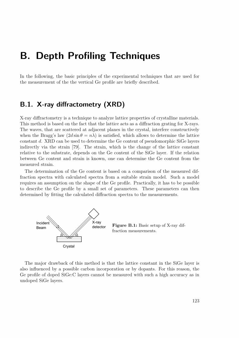
B. Depth Profiling Techniques
In the following, the basic principles of the experimental techniques that are used forthe measurement of the the vertical Ge profile are briefly described.
B.1. X-ray diffractometry (XRD)
X-ray diffractometry is a technique to analyze lattice properties of crystalline materials.This method is based on the fact that the lattice acts as a diffraction grating for X-rays.The waves, that are scattered at adjacent planes in the crystal, interfere constructivelywhen the Bragg’s law (2d sin θ = nλ) is satisfied, which allows to determine the latticeconstant d. XRD can be used to determine the Ge content of pseudomorphic SiGe layersindirectly via the strain [79]. The strain, which is the change of the lattice constantrelative to the substrate, depends on the Ge content of the SiGe layer. If the relationbetween Ge content and strain is known, one can determine the Ge content from themeasured strain.
The determination of the Ge content is based on a comparison of the measured dif-fraction spectra with calculated spectra from a suitable strain model. Such a modelrequires an assumption on the shape of the Ge profile. Practically, it has to be possibleto describe the Ge profile by a small set of parameters. These parameters can thendetermined by fitting the calculated diffraction spectra to the measurements.
Crystal
IncidentBeam
X-ray detector
Θ Θ
Figure B.1: Basic setup of X-ray dif-fraction measurements.
The major drawback of this method is that the lattice constant in the SiGe layer isalso influenced by a possible carbon incorporation or by dopants. For this reason, theGe profile of doped SiGe:C layers cannot be measured with such a high accuracy as inundoped SiGe layers.
123

B. Depth Profiling Techniques
B.2. Secondary Ion Mass Spectroscopy (SIMS)Secondary ion mass spectroscopy is an analytical technique for the characterization ofthe chemical composition of surfaces. In SIMS, atoms and molecules are removed fromthe surface by bombardment with ions. Typical primary ions for the measurement ofdoping profiles in a silicon matrix are O+
2 and Cs+. A small fraction of the removedparticles is emitted as (secondary) ions, which makes it possible to analyze them in amass spectrometer. The rest is emitted as neutral atoms. The efficiency of the ionization(referred to as ion yield) strongly depends on the matrix material and the sputteringenergy.
Figure B.2: Experimental setup of SIMS.Depth profiling is achieved by dynamic re-moval of material during the measurement.
Ion Gun MassSpectrometer
Sample
SputterDirection
For a quantitative analysis in SIMS, the measured ion intensities has to be convertedinto material concentrations. For this purpose, the relative sensitivity factor RSFE forthe element E in the matrix material M is defined according to
IMCM
= RSFE ·IECE
, (B.1)
with the intensities IX and the and concentrations CX . Depth profiles of the materialcomposition can be obtained by continuous measurement over time, while the samplesurface is removed layer by layer. This approach is called dynamic SIMS. It provides adepth resolution down to 0.3 nm [117].
B.3. Energy-Dispersive X-Ray Spectroscopy in a TEMAnother method to determine the elemental composition in solid materials is to useenergy-dispersive X-ray spectroscopy in an electron microscope. The electron beam ofthe microscope generates X-ray emission, which is characteristic of the elements con-tained in the sample. Energy dispersive spectroscopy of the emitted radiation providesinformation on the material composition at the position of the electron beam. Usinga scanning transmission electron microscope (STEM) in EDX mode allows to createspatial maps of the elements distribution in the sample. In this way, depth profiles ofSiGe layers can be measured with a high spatial resolution [78].
A major advantage of this method, compared to SIMS and XRD, is that the materialcomposition can be measured at very small sample areas. This allows the Ge profile tobe measured directly in the transistor which is not possible with SIMS or XRD.
124

B.3. Energy-Dispersive X-Ray Spectroscopy in a TEM
Sample
FocusedElectronBeam
ScanningDirection
EDX Detector
X-ray
Figure B.3: Principle of element analysisby energy dispersive X-ray spectroscopy inan transmission electron microscope.
125


Bibliography[1] J. D. Cressler, “SiGe HBT Technology: A New Contender for Si-Based RF and
Microwave Circuit Applications,” IEEE Transactions on Microwave Theory andTechniques, vol. 46, no. 5, pp. 572–589, 1998.
[2] J. D. Cressler, “A retrospective on the SiGe HBT: What we do know, what wedon’t know, and what we would like to know better,” 2013 IEEE 13th TopicalMeeting on Silicon Monolithic Integrated Circuits in RF Systems, SiRF 2013 -RWW 2013, pp. 81–83, 2013.
[3] H. Rücker, B. Heinemann, and A. Fox, “Half-Terahertz SiGe BiCMOS Techno-logy,” in Silicon Monolithic Integrated Circuits in RF Systems (SiRF), 2012 IEEE12th Topical Meeting on, pp. 133–136, 2012.
[4] A. Margomenos, “A Comparison of Si CMOS and SiGe BiCMOS Technologies forAutomotive Radars,” 2009 9th Topical Meeting on Silicon Monolithic IntegratedCircuits in RF System, SiRF’09 - Digest of Papers, pp. 1–4, 2009.
[5] U. R. Pfeiffer and E. Öjefors, “Terahertz imaging with CMOS/BiCMOS processtechnologies,” ESSCIRC 2010 - 36th European Solid State Circuits Conference,pp. 52–60, 2010.
[6] W. Liebl, J. Boeck, K. Aufinger, et al., “SiGe Applications in Automotive Radars,”ECS Transactions, vol. 75, no. 8, pp. 91–102, 2016.
[7] A. Mai and M. Kaynak, “SiGe-BiCMOS based technology platforms for mm-waveand radar applications,” 2016 21st International Conference on Microwave, Radarand Wireless Communications, MIKON 2016, pp. 4–7, 2016.
[8] G. Sasso, N. Rinaldi, G. Matz, and C. Jungemann, “Accurate Mobility and EnergyRelaxation Time Models for SiGe HBTs Numerical Simulation,” in 2009 Internati-onal Conference on Simulation of Semiconductor Processes and Devices, pp. 241–244, 2009.
[9] G. Sasso, N. Rinaldi, G. Matz, and C. Jungemann, “Analytical Models of EffectiveDOS, Saturation Velocity and High-Field Mobility for SiGe HBTs Numerical Si-mulation,” in Simulation of Semiconductor Processes and Devices (SISPAD), 2010International Conference on, pp. 279–282, 2010.
127

Bibliography
[10] G. Wedel and M. Schröter, “Hydrodynamic simulations for advanced SiGe HBTs,”in Bipolar/BiCMOS Circuits and Technology Meeting (BCTM), 2010 IEEE,pp. 237–244, 2010.
[11] C. Jungemann, A.-T. Pham, S.-M. Hong, L. Smith, and B. Meinerzhagen, “Deter-ministic solvers for the Boltzmann transport equation of 3D and quasi-2D electronand hole systems in SiGe devices,” Solid-State Electronics, vol. 84, pp. 112–119,2013.
[12] R. People and J. C. Bean, “Calculation of critial layer thickness versus lattice mis-match for GexSi1−x/Si strained-layer heterostructures,” Applied Physics Letters,vol. 47, pp. 322–324, 1985.
[13] E. J. Prinz and J. C. Sturm, “Analytical Modeling of Current Gain-Early VoltageProduct in Si/Si1−xGex Heterojunction Bipolar Transistors,” in IEEE Internatio-nal Electron Devices Meeting, pp. 853–856, 1991.
[14] P. Ashburn, SiGe Heterojunction Bipolar Transistors. John Wiley and Sons, Ltd,2003.
[15] J. D. Cressler and G. Niu, Silicon-Germanium Heterojunction Bipolar Transistors.Artech House, 2002.
[16] S. Decoutere, S. Van Huylenbroeck, B. Heinemann, et al., “Advanced ProcessModules and Architectures for Half-Terahertz SiGe:C HBTs,” in Proceedings ofthe IEEE Bipolar/BiCMOS Circuits and Technology Meeting, pp. 9–16, 2009.
[17] M. Schroter, H. Tran, and W. Kraus, “Germanium profile design options for SiGeLEC HBTs,” Solid-State Electronics, vol. 48, no. 7, pp. 1133–1146, 2004.
[18] L. Lanzerotti, A. St. Amour, C. Liu, et al., “Si/Si1−x−y/GexCy/Si heterojunctionbipolar transistors,” IEEE Electron Device Letters, vol. 17, pp. 334–337, jul 1996.
[19] H. Rücker, B. Heinemann, D. Bolze, et al., “Dopant diffusion in C-doped Si andSiGe: Physical model and experimental verification,” Electron Devices Meeting,1999. IEDM Technical Digest. International, pp. 345–348, 1999.
[20] Q. Z. Liu, J. W. Adkisson, V. Jain, et al., “SiGe HBTs in 90nm BiCMOS Techno-logy Demonstrating fT/fMAX 285GHz/475GHz through Simultaneous Reduction ofBase Resistance and Extrinsic Collector Capacitance,” ECS Transactions, vol. 64,no. 6, pp. 285–294, 2014.
[21] B. Heinemann, H. Rücker, R. Barth, et al., “SiGe HBT with fT/fmax of505GHz/720 GHz,” in IEEE International Electron Devices Meeting 2016, 2016.
[22] D. L. Harame, G. Freeman, and J. Rieh, “Look into the Future for SiGe HBTs,” in2003 International Symposium on Compound Semiconductors, pp. 207–208, 2003.
128

Bibliography
[23] P. Chevalier, T. F. Meister, B. Heinemann, et al., “Towards THz SiGe HBTs,” in2011 IEEE Bipolar/BiCMOS Circuits and Technology Meeting, pp. 57–65, 2011.
[24] M. Khater, J.-S. Rieh, T. Adam, et al., “SiGe HBT Technology with fmax/fT =350/300 GHz and Gate Delay below 3.3 ps,” in IEEE International Electron De-vices Meeting 2004, pp. 247–250, 2004.
[25] R. Lachner, “Towards 0.7 Terahertz Silicon Germanium Heterojunction BipolarTechnology – The DOTSEVEN Project,” ECS Transactions, vol. 64, pp. 21–37,aug 2014.
[26] B. Heinemann, R. Barth, D. Bolze, et al., “SiGe HBT technology with fT/fmaxof 300GHz/500GHz and 2.0ps CML gate delay,” in Electron Devices Meeting(IEDM), 2010 IEEE International, pp. 30.5.1–30.5.4, 2010.
[27] J. Böck, K. Aufinger, S. Boguth, et al., “SiGe HBT and BiCMOS Process Integra-tion Optimization within the DOTSEVEN Project,” in Bipolar/BiCMOS Circuitsand Technology Meeting (BCTM), pp. 121–124, 2015.
[28] P. Chevalier, G. Avenier, G. Ribes, et al., “A 55 nm Triple Gate Oxide 9 MetalLayers SiGe BiCMOS Technology Featuring 320 GHz fT 370 GHz fMAX HBTand High-Q Millimeter-Wave Passives,” in IEEE International Electron DevicesMeeting, pp. 3.9.1–3.9.3, 2014.
[29] V. P. Trivedi, J. P. John, J. Young, et al., “A 90nm BiCMOS technology fea-turing 400GHz fMAX SiGe:C HBT,” 2016 IEEE Bipolar/BiCMOS Circuits andTechnology Meeting (BCTM), pp. 60–63, 2016.
[30] J. J. Pekarik, J. Adkisson, P. Gray, et al., “A 90nm SiGe BiCMOS technology formm-wave and high-performance analog applications,” in Proceedings of the IEEEBipolar/BiCMOS Circuits and Technology Meeting, pp. 92–95, 2014.
[31] P. Hurwitz, R. Kanawati, K. Moen, et al., “Advances in RF foundry technologyfor wireless and wireline communications,” SiRF 2016 - 2016 IEEE 16th TopicalMeeting on Silicon Monolithic Integrated Circuits in RF Systems, pp. 5–8, 2016.
[32] S. Li and Y. Fu, 3D TCAD Simulation for Semiconductor Processes, Devices andOptoelectronics. Springer-Verlag New York, 2012.
[33] T. Grasser, H. Kosina, and S. Selberherr, “Investigation of spurious velocity overs-hoot using Monte Carlo data,” Applied Physics Letters, vol. 79, no. 12, pp. 1900–1902, 2001.
[34] R. Kosik, Numerical Challenges on the Road to NanoTCAD. PhD thesis, Technis-chen Universität Wien, 2004.
129

Bibliography
[35] S. Keith, C. Jungemann, S. Decker, et al., “Full-band Monte Carlo device simu-lation of a Si/SiGe-HBT with a realistic Ge profile,” in International Conferenceon Simulation of Semiconductor Processes and Devices (SISPAD), pp. 219–222,1999.
[36] S. M. Hong and C. Jungemann, “Electron transport in extremely scaled SiGeHBTs,” Proceedings of the IEEE Bipolar/BiCMOS Circuits and Technology Meet-ing, pp. 67–74, 2009.
[37] Synopsys, “Sentaurus Device User Guide,” 2016.
[38] M. Al-Sa’di, V. D’Alessandro, S. Fregonese, et al., “TCAD simulation and deve-lopment within the European DOTFIVE project on 500 GHz SiGe:C HBTs,” inMicrowave Integrated Circuits Conference (EuMIC), pp. 29–32, 2010.
[39] G. L. Patton, S. S. Iyer, S. L. Delage, S. Tiwari, and J. M. Stork, “Silicon-Germanium-Base Heteroiunction Bipolar Transistors By Molecular Beam Epi-taxy,” IEEE Electron Device Letters, vol. 9, no. 4, pp. 65–67, 1988.
[40] C. King, J. Hoyt, and J. Gibbons, “Bandgap and transport properties of Si1−xGexby analysis of nearly ideal Si/Si1−xGex/Si heterojunction bipolar transistors,”IEEE Transactions on Electron Devices, vol. 36, no. 10, pp. 2093–2104, 1989.
[41] S. Jain, J. Poortmans, S. Iyer, et al., “Electrical and optical bandgaps of GexSi1−xstrained layers,” IEEE Transactions on Electron Devices, vol. 40, no. 12, pp. 2338–2343, 1993.
[42] Z. Matutinovic-Krstelj, V. Venkataraman, E. J. Prinz, J. C. Sturm, and C. W.Magee, “Base resistance and effective bandgap reduction in n-p-n Si/Si1−xGex/SiHBTs with heavy base doping,” Electron Devices, IEEE Transactions on, vol. 43,no. 3, pp. 457–466, 1996.
[43] I. Anteney, G. Lippert, P. Ashburn, et al., “Electrical determination of bandgapnarrowing and parasitic energy barriers in SiGe and SiGeC heterojunction bipolartransistors,” in Workshop on High Performance Electron Devices for Microwaveand Optoelectronic Applications, vol. 2, pp. 55–60, 1997.
[44] J. Eberhardt and E. Kasper, “Bandgap narrowing in strained SiGe on the basisof electrical measurements on Si/SiGe/Si hetero bipolar transistors,” MaterialsScience and Engineering: B, vol. 89, pp. 93–96, feb 2002.
[45] M. Lundstrom, Fundamentals of Carrier Transport. Cambridge University Press,2000.
[46] T. Grasser, T. W. Tang, H. Kosina, and S. Selberherr, “A Review of Hydrodynamicand Energy-Eransport Models for Semiconductor Device Simulation,” Proceedingsof the IEEE, vol. 91, no. 2, pp. 251–273, 2003.
130

Bibliography
[47] D. Ventura, A. Gnudi, G. Baccarani, and F. Odeh, “Multidimensional SphericalHarmonics Expansion of Boltzmann Equation for Transport in Semiconductors,”Applied Mathematics Letters, vol. 5, pp. 85–90, may 1992.
[48] T. Grasser, H. Kosina, M. Gritsch, and S. Selberherr, “Using six moments ofBoltzmann’s transport equation for device simulation,” Journal of Applied Physics,vol. 90, no. 5, pp. 2389–2396, 2001.
[49] K. Blotekjaer, “Transport equations for electrons in two-valley semiconductors,”IEEE Transactions on Electron Devices, vol. 17, no. 1, pp. 38–47, 1970.
[50] A. Schenk, Advanced Physical Models for Silicon Device Simulation. Springer-Verlag Wien, 1998.
[51] R. Stratton, “Diffusion of Hot and Cold Electrons in Semiconductor Barriers,”Phys. Rev., vol. 126, pp. 2002–2014, jun 1962.
[52] E. Azoff, “Generalized energy-momentum conservation equations in the relaxationtime approximation,” Solid-State Electronics, vol. 30, pp. 913–917, sep 1987.
[53] Dotfive, “Website of the Dotfive Projekt,” 2011.
[54] B. Gonzalez, V. Palankovski, H. Kosina, A. Hernandez, and S. Selberherr, “Anenergy relaxation time model for device simulation,” Solid-State Electronics,vol. 43, pp. 1791–1795, sep 1999.
[55] D. M. Caughey and R. E. Thomas, “Carrier Mobilities in Silicon EmpiricallyRelated to the Doping and Field,” Proceedings of the IEEE, vol. 55, no. 11, pp. 2192– 2193, 1967.
[56] W. Hänsch, M. Orlowski, and W. Weber, “THE HOT-ELECTRON PROBLEMIN SUBMICRON MOSFET,” Le Journal de Physique Colloques, vol. 49, pp. C4–597–C4–606, sep 1988.
[57] G. Masetti, M. Severi, and S. Solmi, “Modeling of Carrier Mobility Against CarrierConcentration in Arsenic-Doped, Phosphorus-Doped, and Boron-Doped Silicon,”IEEE Transactions on Electron Devices, vol. 30, no. 7, pp. 764–769, 1983.
[58] S. Reggiani, M. Valdinoci, L. Colalongo, et al., “Electron and hole mobility insilicon at large operating temperatures - Part I: Bulk mobility,” IEEE Transactionson Electron Devices, vol. 49, no. 3, pp. 490–499, 2002.
[59] G. Sasso, Transport Models and Advanced Numerical Simulation of Silicon-Germanium Heterojunction Bipolar Transistors. PhD thesis, University of NaplesFederico II, 2010.
[60] H. Kroemer, “Two integral relations pertaining to the electron transport througha bipolar transistor with a nonuniform energy gap in the base region,” Solid StateElectronics, vol. 28, no. 11, pp. 1101–1103, 1985.
131

Bibliography
[61] D. B. M. Klaassen, J. W. Slotboom, and H. C. De Graaff, “Unified apparentbandgap narrowing in n- and p-type silicon,” Solid-State Electronics, vol. 35, no. 2,pp. 125–129, 1992.
[62] F. Bärwolf, I. Costina, Y. Yamamoto, and A. Scheit, “DSIMS Quantitative Ca-libration and Analysis of Dopant Concentration in Homogeneously and GradedSiGe Layer,” in SIMS Europe Münster, 2016.
[63] B. Barbalat, T. Schwartzmann, P. Chevalier, et al., “The effect of carbon on neu-tral base recombination in high-speed SiGeC heterojunction bipolar transistors,”Semiconductor Science and Technology, vol. 22, no. 1, pp. 99–102, 2007.
[64] J. Sturm, “Si/SiGe/Si heterojunction bipolar transistors,” in Properties of strainedand relaxed Silicon Germanium (E. Kasper, ed.), ch. 7, pp. 193–204, inspec, 1995.
[65] S. Swirhun, Y.-H. Kwark, and R. Swanson, “Measurement of electron lifetime,electron mobility and band-gap narrowing in heavily doped p-type silicon,” 1986International Electron Devices Meeting, vol. 32, pp. 0–3, 1986.
[66] E. J. Prinz, P. M. Garone, P. V. Schwartz, X. Xiao, and J. C. Sturm, “The effect ofbase-emitter spacers and strain dependent densities of states in Si/Si1−xGex/Si he-terojunction bipolar transistors,” in IEEE International Electron Devices Meeting,pp. 639–642, 1989.
[67] F. M. Bufler, Full-Band Monte Carlo Simulation of Electrons and Holes in StrainedSi and SiGe. PhD thesis, Universität Bremen, 1998.
[68] C. G. Van de Walle, “Theoretical calculations of semiconductor heterojunctiondiscontinuities,” Journal of Vacuum Science and Technology B: Microelectronicsand Nanometer Structures, vol. 4, no. 8, p. 1055, 1986.
[69] A. S. Amour, C. W. Liu, J. C. Sturm, Y. Lacroix, and M. L. W. Thewalt, “Defect-free band-edge photoluminescence and band gap measurement of pseudomorphicSiGeC alloy layers on Si (100),” Applied Physics Letters, vol. 67, no. 26, p. 3915,1995.
[70] K. Yuki, K. Toyoda, T. Takagi, et al., “Bandgap and Strain Engineering in SiGeCHeterojunction Bipolar Transistors,” Japanese Journal of Applied Physics, vol. 40,no. 4, pp. 2633–2636, 2001.
[71] Y. Varshni, “Temperature dependence of the energy gap in semiconductors,” Phy-sica, vol. 34, pp. 149–154, jan 1967.
[72] R. Braunstein, A. Moore, and F. Herman, “Intrinsic Optical Absorption inGermanium-Silicon Alloys,” Physical Review, vol. 109, no. 3, pp. 695–710, 1958.
132

Bibliography
[73] M. Schröter, T. Rosenbaum, P. Chevalier, et al., “SiGe HBT Technology: FutureTrends and TCAD-Based Roadmap,” Proceedings of the IEEE, vol. PP, no. 99,pp. 1–19, 2016.
[74] T. Rosenbaum, O. Saxod, V. T. Vu, et al., “Calibration of 1D doping profiles ofSiGe HBTs,” in 2015 IEEE Bipolar/BiCMOS Circuits and Technology Meeting -BCTM, pp. 64–67, 2015.
[75] M. Schröter, G. Wedel, B. Heinemann, et al., “Physical and Electrical PerformanceLimits of High-Speed SiGeC HBTs—Part I: Vertical Scaling,” IEEE Transactionson Electron Devices, vol. 58, no. 11, pp. 3687–3796, 2011.
[76] J. Korn, H. Rücker, B. Heinemann, et al., “Experimental and theoretical studyof fT for SiGe HBTs with a scaled vertical doping profile,” in Bipolar/BiCMOSCircuits and Technology Meeting - BCTM, 2015 IEEE, pp. 117–120, 2015.
[77] A. Pawlak, S. Lehmann, and M. Schröter, “A Simple and Accurate Method forExtracting the Emitter and Thermal Resistance of BJTs and HBTs,” in Bipo-lar/BiCMOS Circuits and Technology Meeting - BCTM, 2014 IEEE, pp. 175–178,2014.
[78] M. A. Schubert, P. Zaumseil, I. Costina, and H. Rücker, “Quantitative energy dis-persive X-ray spectroscopy on thin SiGe layers,” in The 16th European MicroscopyCongress, 2016.
[79] P. Zaumseil, D. Krüger, and R. Kurps, “Precise Measurement of Ge Depth Profilesin SiGe HBT’s - a Comparison of Different Methods,” Solid State Phenomena,vol. 95, pp. 473–482, 2003.
[80] Synopsys, “TCAD Sentaurus Release Notes Version M-2016.12 (STAR No.9001056792),” tech. rep., Synopsys Inc., 2016.
[81] H. Rücker, B. Heinemann, R. Barth, and M. Lisker, “Impact of back end stresson SiGe bipolar transistors,” in Electron Devices Meeting (IEDM), 2011 IEEEInternational, pp. 34.5.1–34.5.4, 2011.
[82] D. J. Paul, “Si/SiGe heterostructures: from material and physics to devices andcircuits,” Semiconductor Science and Technology, vol. 19, no. 10, pp. R75–R108,2004.
[83] M. Schröter and S. Lehmann, “The rectangular bipolar transistor tetrode struc-ture and its application,” IEEE International Conference on Microelectronic TestStructures, pp. 206–209, 2007.
[84] T. Grasser, R. Quay, V. Palankovski, and S. Selberherr, “A global self-heatingmodel for device simulation,” in European Solid-State Device Research Conference,pp. 324–327, 2000.
133

Bibliography
[85] A. Magnani, G. Sasso, V. Alessandro, et al., “Advanced thermal resistance simula-tion of SiGe HBTs including backend cooling effect,” in Thermal Investigations ofICs and Systems (THERMINIC), 2015 21st International Workshop on, pp. 1–5,2015.
[86] H. Kamrani, D. Jabs, V. Alessandro, et al., “A Deterministic and Self-ConsistentSolver for the Coupled Carrier-Phonon System in SiGe HBTs,” IEEE Transactionson Electron Devices, vol. 64, no. 2, pp. 361–367, 2017.
[87] V. D’Alessandro and N. Rinaldi, “A critical review of thermal models for electro-thermal simulation,” Solid-State Electronics, vol. 46, no. 4, pp. 487–496, 2002.
[88] S. J. Mason, “Power Gain in Feedback Amplifier,” Transactions of the IRE Pro-fessional Group on Circuit Theory, vol. CT-1, no. 2, pp. 20–25, 1954.
[89] G. A. M. Hurkx, D. B. M. Klaassen, and M. P. G. Knuvers, “A New RecombinationModel for Device Simulation Including Tunneling,” IEEE Transactions on ElectronDevices, vol. 39, no. 2, pp. 331–338, 1992.
[90] A. Gruhle, “The Influence of Emitter-Base Junction Design on Collector Satura-tion Current, Ideality Factor, Early Voltage and Device Switching Speed of Si /SiGe HBT’s,” IEEE Transactions on Electron Devices, vol. 41, no. 2, pp. 198–203,1994.
[91] H. K. Gummel and H. C. Poon, “An Integral Charge Control Model of BipolarTransistors,” Bell System Technical Journal, vol. 49, no. 5, pp. 827–852, 1970.
[92] M. Schröter and A. Chakravorty, Compact Hierarchical Bipolar Transistor Mo-deling with HICUM. World Scientific, 2010.
[93] A. Pawlak, M. Schröter, and A. Fox, “Geometry Scalable Model Parameter Ex-traction for mm-Wave SiGe-Heterojunction Transistors,” in Proceedings of theIEEE Bipolar/BiCMOS Circuits and Technology Meeting, pp. 127–130, 2013.
[94] A. Pawlak and M. Schröter, “Modeling of SiGe HBTs with (fT , fmax) of (340,560) GHz based on physics-based scalable model parmeter extraction,” in IEEE17th Topical Meeting on Silicon Monolithic Integrated Circuits in RF Systems,pp. 100–102, 2017.
[95] S. Selberherr, Analysis and Simulation of Semiconductor Devices. Springer Vienna,1984.
[96] H. K. Gummel, “A Charge Control Relation for Bipolar Transistors,” The BellSystem Technical Journal, vol. 49, no. 1, pp. 115–120, 1970.
[97] B. Heinemann, 2D-Bauelementesimulation der elektischen Eigenschaften vonSiGe-HBTs. PhD thesis, Technische Universität Berlin, 1997.
134

Bibliography
[98] J. J. H. van den Biesen, “A Simple Regional Analysis of Transit Times in BipolarTransistors,” Solid State Electronics, vol. 29, no. 5, pp. 529–534, 1986.
[99] M. Schröter and H. Tran, “Charge-storage related parameter calculation for Si andSiGe bipolar transistors from device simulation,” in WCM, International Nano-Tech Meeting, Boston (MA), vol. 3, pp. 735–740, 2006.
[100] P. Agarwal, G. Hurkx, J. Donkers, and J. Slotboom, “On the delay times invertically scaled SiGe HBTs,” Proceedings of the Bipolar/BiCMOS Circuits andTechnology Meeting, 2005., pp. 264–267, 2005.
[101] P. Palestri, M. Mastrapasqua, A. Pacelli, and C. A. King, “A Drift-Diffusion /Monte Carlo Simulation Methodology for Si1−xGex HBT Design,” IEEE Tran-sactions on Electron Devices, vol. 49, no. 7, pp. 1242–1249, 2002.
[102] Y. Shi and G. Niu, “Vertical Profile Design and Transit Time Analysis of Nano-Scale SiGe HBTs for Terahertz fT ,” in Bipolar/BiCMOS Circuits and TechnologyMeeting (BCTM), pp. 213–216, 2004.
[103] J. Kirk, C.T., “A Theory of Transistor Cutoff Frequency (fT ) Falloff at HighCurrent Densities,” IRE Transactions on Electron Devices, vol. 9, no. 2, pp. 164–174, 1962.
[104] R. J. E. Hueting, J. W. Slotboom, A. Pruijmboom, et al., “On the Optimization ofSiGe-Base Bipolar Transistors,” IEEE Transactions on Electron Devices, vol. 43,no. 9, pp. 1518–1524, 1996.
[105] G. Wedel, “Terahertz SiGe HBT TCAD and numerical device simulation,” in IEEECompound Semiconductor Integrated Circuit Symposium (CSICS) - Short Course,2016.
[106] W. Kloosterman, J. Paasschens, and D. Klaassen, “Improved extraction of baseand emitter resistance from small signal high frequency admittance measure-ments,” Bipolar/BiCMOS Circuits and Technology Meeting, 1999. Proceedings ofthe 1999, pp. 93–96, 1999.
[107] J. Berkner, Kompaktmodelle für Bipolartransistoren. Expert Verlag Renningen,2002.
[108] H. Rücker, B. Heinemann, W. Winkler, et al., “A 0 .13µm SiGe BiCMOS Techno-logy Featuring fT/fmax of 240GHz/330GHz and Gate Delays Below 3ps,” Solid-State Circuits, IEEE Journal of, vol. 45, no. 9, pp. 1678–1686, 2010.
[109] J. Slotboom, G. Streutker, a. Pruijmboom, and D. Gravesteijn, “Parasitic energybarriers in SiGe HBTs,” IEEE Electron Device Letters, vol. 12, no. 9, pp. 486–488,1991.
135

Bibliography
[110] Z. A. Shafi, C. J. Gibbings, P. Ashburn, et al., “The Importance of NeutralBase Recombination in Compromising the Gain of Si/SiGe Heterojunction BipolarTransistors,” IEEE Transactions on Electron Devices, vol. 38, no. 8, pp. 1973–1976,1991.
[111] A. J. Joseph, J. D. Cressler, D. M. Richey, and R. C. Jaeger, “Neutral Base Recom-bination and its Influence on the Temperature Tependence of Early Voltage andCurrent Gain-Early Voltage Product in UHV/CVD SiGe Heterojunction BipolarTransistors,” IEEE Transactions on Electron Devices, vol. 44, no. 3, pp. 404–413,1997.
[112] S.-I. Kim, B. R. Ryum, S.-W. Kang, and W. Kim, “The Effect of a Parasitic Poten-tial Barrier on the Neutral Base Recombination Current of Si/SiGe/Si DHBTs,”Solid-State Electronics, vol. 37, pp. 517–519, mar 1994.
[113] G. Niu, J. D. Cressler, and A. J. Joseph, “Quantifying Neutral Base Recombinationand the Effects of Collector-Base Junction Traps in UHV/CVD SiGe HBT’s,”IEEE Transactions on Electron Devices, vol. 45, no. 12, pp. 2499–2504, 1998.
[114] S. Reggiani, E. Gnani, M. Rudan, et al., “Measurement and Modeling of theElectron Impact-Ionization Coefficient in Silicon Up to Very High Temperatures,”IEEE Transactions on Electron Devices, vol. 52, no. 10, pp. 2290–2297, 2005.
[115] J. D. Hayden, D. Burnett, and J. Nangle, “A Comparison of Base Current Reversaland Bipolar Snapback in Advanced N-P-N Bipolar Transistors,” IEEE ElectronDevice Letters, vol. 12, no. 8, pp. 407–409, 1991.
[116] A. Schenk, “Finite-temperature full random-phase approximation model of bandgap narrowing for silicon device simulation,” Journal of Applied Physics, vol. 84,no. 7, pp. 3684–3695, 1998.
[117] H. Czichos, T. Saito, and L. Smith, Spinger Handbook of Materials MeasurementMethods. Springer, 2006.
136

List of Figures1.1. Schematic band diagram of a SiGe HBT . . . . . . . . . . . . . . . . . . 31.2. Schematic cross section of a high-performance SiGe HBT from IHPs
0.13µm technology SG13G2. . . . . . . . . . . . . . . . . . . . . . . . . . 51.3. Published values of fT and fmax from several high-speed SiGe HBT techno-
logies . . . . . . . . . . . . . . . . . . . . . . . . . . . . . . . . . . . . . . 6
2.1. Electron energy relaxation time as a function of the normalized electrontemperature for different Ge mole fractions x. . . . . . . . . . . . . . . . 18
2.2. Minority electron mobility in silicon as function of acceptor doping con-centration. . . . . . . . . . . . . . . . . . . . . . . . . . . . . . . . . . . . 20
2.3. Minority electron mobility for different germanium percentages (T = 300 K). 202.4. Electron saturation velocity as a function of the Ge mole fraction (T =
300 K). . . . . . . . . . . . . . . . . . . . . . . . . . . . . . . . . . . . . . 212.5. Field dependence of the minority electron mobility (T = 300 K, NA =
1017 cm−3). . . . . . . . . . . . . . . . . . . . . . . . . . . . . . . . . . . 212.6. Effective density of states in the conduction and the valence band as a
function of the Ge mole fraction. . . . . . . . . . . . . . . . . . . . . . . 222.7. Doping-induced bandgap narrowing. Original values from Klaassen et
al. [61] and the recalculated values which are consistent with the dotfivemobility model. . . . . . . . . . . . . . . . . . . . . . . . . . . . . . . . . 24
2.8. TEM cross section of a SiGe HBT fabricated in the simplified process. . . 252.9. Ge concentration from SIMS and X-ray diffraction. . . . . . . . . . . . . 252.10. Typical SIMS profile of the box-like SiGe base. This profile corresponds
to wafer 16 from Tab. 2.1. . . . . . . . . . . . . . . . . . . . . . . . . . . 262.11. Vertical transistor profile and simulated electron and hole density at zero
bias. . . . . . . . . . . . . . . . . . . . . . . . . . . . . . . . . . . . . . . 262.12. Gummel characteristics for different Ge percentages. Solid lines represent
the collector current and dashed lines represent the base current. . . . . . 282.13. Bandgap as a function of the germanium mole fraction. Symbols show
data obtained in this work. Lines show values from Sturm [64] and Eber-hardt [44] as well as default values from Sentaurus Device. . . . . . . . . 28
2.14. Collector current of the all-silicon transistor measured at 233 K, 293 K,353 K, 413 K and 473 K. . . . . . . . . . . . . . . . . . . . . . . . . . . . 30
2.15. Temperature dependence of the effective bandgap for 0 %, 8.4 %, 21 % and30.7 % germanium. . . . . . . . . . . . . . . . . . . . . . . . . . . . . . . 30
2.16. Measured and simulated collector current as a function of VEB for thefour wafer splits with different Ge fraction . . . . . . . . . . . . . . . . . 31
137

List of Figures
3.1. TEM cross section of the HBT. . . . . . . . . . . . . . . . . . . . . . . . 343.2. Different transistor layouts . . . . . . . . . . . . . . . . . . . . . . . . . . 353.3. Measured Gummel characteristics of device D0 . . . . . . . . . . . . . . . 353.4. fT and fmax as a function of the collector current density. . . . . . . . . . 353.5. Measured depth profile of the base doping (SIMS, EDX). . . . . . . . . . 373.6. Influence of the thermal budget on the base profile. . . . . . . . . . . . . 383.7. EDX line scan over the SiGe layer at a sample from the transistor and a
sample from the large SIMS monitor. . . . . . . . . . . . . . . . . . . . . 393.8. HBT cross section: TEM image and simulation structure. . . . . . . . . . 403.9. Vertical doping profile used in the simulation. . . . . . . . . . . . . . . . 413.10. Measured and simulated capacitance. . . . . . . . . . . . . . . . . . . . . 423.11. Collector current scaling . . . . . . . . . . . . . . . . . . . . . . . . . . . 433.12. Bandgap as a function of the germanium mole fraction. . . . . . . . . . . 433.13. Layout and schematic cross-section of the tetrode transistor structure. . . 453.14. Comparison between full electro-thermal simulation and the global self-
heating model. . . . . . . . . . . . . . . . . . . . . . . . . . . . . . . . . 473.15. Distribution of the lattice temperature TL at VBE = 0.9 V. . . . . . . . . 473.16. Cross-sections of TL and the small-signal temperature response. . . . . . 473.17. Calculated current gain h21 and unilateral power gain as well as fT and
fmax. . . . . . . . . . . . . . . . . . . . . . . . . . . . . . . . . . . . . . . 493.18. Measured and simulated gummel characteristics and the ideality of the
collector current nIC of device D2. . . . . . . . . . . . . . . . . . . . . . . 503.19. Measured and simulated fT and fMAX of device D2 at VCB = 0V . . . . . 503.20. Simulated electrical characteristics for different values of fhf . . . . . . . 513.21. Impact of bandgap-narrowing on simulated IC . . . . . . . . . . . . . . . . 533.22. Vertical profile, bandgap and conduction band energy as a function of
depth. . . . . . . . . . . . . . . . . . . . . . . . . . . . . . . . . . . . . . 543.23. Measured and simulated IC as well as simulated lattice temperature TL
as a function of VBE at a VCB of 0.5 V, 0 V and −0.5 V. . . . . . . . . . . 553.24. Measured and simulated output characteristics at a fixed VBE of 0.7 V,
0.86 V and 0.9 V. . . . . . . . . . . . . . . . . . . . . . . . . . . . . . . . 563.25. Measured and simulated fT for different emitter geometries. VCB = 0 V. . 573.26. Measured and simulated fT for different VCB for D2. . . . . . . . . . . . 573.27. Measured and simulated fT for D2 at VCB = 0 V. . . . . . . . . . . . . . 583.28. Measured and simulated IC as a function VBE for D2 at VCB = 0 V. . . . 583.29. Regional transit times for HD and DD simulation. . . . . . . . . . . . . . 603.30. Internal variables from DD simulation. . . . . . . . . . . . . . . . . . . . 613.31. Internal variables from HD simulation. . . . . . . . . . . . . . . . . . . . 633.32. Impact of parasitic elements from 2D simulation. . . . . . . . . . . . . . 643.33. Overview on the impact of different parasitics. . . . . . . . . . . . . . . . 653.34. Sketch of the 2D and 1D simulation configuration. . . . . . . . . . . . . . 653.35. Comparison between 1D and 2D simulation. . . . . . . . . . . . . . . . . 663.36. fT -characteristics of D2 simulated with the HICUM compact model. Ex-
ternal parasitics are successively switched off. . . . . . . . . . . . . . . . 67
138

List of Figures
4.1. Sketch of the 2D domain which is used to simulate the inner transistor. . 714.2. Comparison of fT from quasi-static simulation (QS) and from small-signal
AC simulation. . . . . . . . . . . . . . . . . . . . . . . . . . . . . . . . . 724.3. Distribution of the transit time in the 1D transistor at peak fT . . . . . . 734.4. Simple high-frequency small-signal equivalent circuit of a bipolar transistor. 764.5. Measured (2πfT )−1 as a function of inverse transconductance. Extrapo-
lation from linear region yields τf . . . . . . . . . . . . . . . . . . . . . . . 774.6. Simulated transit time τec and its regional contributions as a function of
inverse gm. . . . . . . . . . . . . . . . . . . . . . . . . . . . . . . . . . . . 774.7. Regional transit times for different configurations of 1D and 2D simulation. 794.8. Measured τec, fT and IC for profile variations with increasing cap thickness. 804.9. 1D quasi-static simulations with different doping profiles at the EB junction. 814.10. Regional transit times as a function of the collector current. . . . . . . . 824.11. Band structure of the different profiles at VBE = 0.91 V. . . . . . . . . . . 834.12. Measured τec for HBTs with different SIC doping. . . . . . . . . . . . . . 834.13. Simulation results for different SIC doping. . . . . . . . . . . . . . . . . . 844.14. Regional transit times for different variants of the selectively implanted
collector. . . . . . . . . . . . . . . . . . . . . . . . . . . . . . . . . . . . . 854.15. Measured τec for different Ge profiles. . . . . . . . . . . . . . . . . . . . . 864.16. 1D Simulation results for different Ge profiles. . . . . . . . . . . . . . . . 874.17. Spatial distribution of the quasi-static electron and hole density response
at IC = 5mA/µm . . . . . . . . . . . . . . . . . . . . . . . . . . . . . . . 884.18. 2D Simulation results for different Ge profiles. . . . . . . . . . . . . . . . 894.19. fT from 1D quasi-static simulation for different EB junction widths. . . . 894.20. Comparison of experimental profile P0 with hypothetical profile N3. . . . 904.21. Regional transit times as a function of the collector current for profiles
P0 and N3. . . . . . . . . . . . . . . . . . . . . . . . . . . . . . . . . . . 914.22. Variations of the experimental profile using the emitter and Ge profile of
N3. . . . . . . . . . . . . . . . . . . . . . . . . . . . . . . . . . . . . . . . 924.23. fT as a function of IC from 1D quasi static simulation. f) Gummel plot. 924.24. Impact of the emitter and Ge profile on the regional transit times. . . . . 934.25. Comparison of collector profiles. . . . . . . . . . . . . . . . . . . . . . . . 944.26. Variations of the vertical profile. . . . . . . . . . . . . . . . . . . . . . . . 954.27. Variations of the base profile. . . . . . . . . . . . . . . . . . . . . . . . . 974.28. 2D simulation of fT as a function of IC for different vertical doping profiles
at VCB = 0 V. . . . . . . . . . . . . . . . . . . . . . . . . . . . . . . . . . 97
5.1. Geometry of the 2D simulation domain which represents one half of theHBT. . . . . . . . . . . . . . . . . . . . . . . . . . . . . . . . . . . . . . . 99
5.2. Influence of the emitter width on the characteristics of the HBT. . . . . . 1015.3. Doping of the base link region . . . . . . . . . . . . . . . . . . . . . . . . 1035.4. Impact of boron out-diffusion from the external base on fT (a) and fmax
(b). . . . . . . . . . . . . . . . . . . . . . . . . . . . . . . . . . . . . . . . 104
139

List of Figures
5.5. Quasi-static change of the electron density ∆n for the two different degreesof boron out-diffusion. . . . . . . . . . . . . . . . . . . . . . . . . . . . . 105
5.6. 1D plot to illustrate charge storage in the external base. . . . . . . . . . 1065.7. Simulated base current as a function of VCB. . . . . . . . . . . . . . . . . 1075.8. Measured base current as a function of VCB for HBTs with different widths
of the polysilicon emitter. . . . . . . . . . . . . . . . . . . . . . . . . . . 1075.9. Impact of the collector window width WCW . . . . . . . . . . . . . . . . . 1095.10. Quasi-static change of the electron density for WCX = 0 nm and WCX =
55 nm . . . . . . . . . . . . . . . . . . . . . . . . . . . . . . . . . . . . . 1095.11. 2D doping profile for an oxide thickness of 80 nm and 40 nm. . . . . . . . 1105.12. Impact of the oxide thickness HOX on fT with WCX = 55 nm. . . . . . . 1115.13. Impact of the oxide thickness HOX on fT with WCX = 0 nm. . . . . . . . 1125.14. Output characteristics in common-base configuration with fixed emitter
current. . . . . . . . . . . . . . . . . . . . . . . . . . . . . . . . . . . . . 1135.15. Absolute value of the base current as a function of VCE. . . . . . . . . . . 1135.16. Reference structure G2 and scaled structure D7. . . . . . . . . . . . . . . 1145.17. fT and fmax as a function of IC . . . . . . . . . . . . . . . . . . . . . . . . 115
B.1. Basic setup of X-ray diffraction measurements. . . . . . . . . . . . . . . . 123B.2. Experimental setup of SIMS. Depth profiling is achieved by dynamic re-
moval of material during the measurement. . . . . . . . . . . . . . . . . . 124B.3. Principle of element analysis by energy dispersive X-ray spectroscopy in
an transmission electron microscope. . . . . . . . . . . . . . . . . . . . . 125
140

List of Tables2.1. Parameters of wafer splits with different material composition in the HBT
base. . . . . . . . . . . . . . . . . . . . . . . . . . . . . . . . . . . . . . . 27
3.1. Measured electrical parameters of the HBTs. . . . . . . . . . . . . . . . . 36
5.1. Simulated electrical parameters. The second and third columns containthe profile variant in lateral and vertical direction. . . . . . . . . . . . . . 104
5.2. Simulated device parameters for different width of the collector windowWC and two variations of the p-doping profile at the external base link. . 108
5.3. Simulated Device Parameters . . . . . . . . . . . . . . . . . . . . . . . . 1125.4. Simulated device darameters for various modifications of the HBT structure.115
A.1. Parameter values are taken from [8]. . . . . . . . . . . . . . . . . . . . . 119A.2. Parameters for Si taken from [8]. Normalized temperature Tn = T/300K. 119A.3. Parameters for Si0.7Ge0.3 taken from [8]. Tn is the normalized temperature
Tn = T/300K. . . . . . . . . . . . . . . . . . . . . . . . . . . . . . . . . . 120A.4. Parameters for interpolation between Si and Si0.7Ge0.3 taken from [8]. . . 120A.5. Fitted parameters for the high-field mobility. . . . . . . . . . . . . . . . . 121A.6. Parameter values are taken from [9]. . . . . . . . . . . . . . . . . . . . . 122
141


List of Abbreviations and Symbols
Abbreviations
BC Base-CollectorBE Base-EmitterBGN Bandgap NarrowingBJT Bipolar Junction TransistorBTE Boltzmann Transport EquationCMOS Complementary Metal-Oxide-SemiconductorDD Drift-DiffusionDOS Density of StatesDPSA Double Poly-Silicon Self-Aligned (emitter/base)EAG Evans Analytical GroupEDX Energy Dispersive X-ray SpectroscopyET Energy TransportFOM Figure of MeritHBT Heterojunction Bipolar TransistorHD HydrodynamicHICUM High Current ModelITRS International Technology Roadmap for SemiconductorsMC Monte CarloMOSFET Metal-Oxide-Semiconductor Field-Effect TransistorNBR Neutral Base RecombinationQS Quasi-StaticRF Radio FrequencySCR Space Charge RegionSEG Selective Epitaxially Grown (base)SHE Spherical Harmonics ExpansionSiGe(C) Silicon Germanium (Carbon)SIC Selectively Implanted CollectorSIMS Secondary Ion Mass SpectroscopySRH Shockley-Read-HallTCAD Technology Computer Aided DesignTEM Transmission Electron MicroscopeRSF Relative Sensitivity FactorRTA Rapid Thermal AnnealingXRD X-ray Diffractometry
143

List of Abbreviations and Symbols
Symbols
β Current gainCjEB Base-emitter depletion capacitanceCdEB Base-emitter diffusion capacitanceCEBi Internal base-collector capacitanceCEBx External base-collector capacitance∆Eg,dop Doping induced bandgap narrowing∆Eg,Ge Bandgap reduction due to germaniumDn Electron diffusivityEC/EV Conduction/valence band energyEFn/EFp Quasi Fermi energy of electrons/holesEg BandgapEg,eff Effective bandgap in SiGe (including bandgap narrowing)Eg,Si Bandgap in (undoped) siliconfmax Maximum oscillation frequencyfT Transit frequencyfhf Heat flux parameterf td Thermal diffusion parametergm Transconductanceh21 Small-signal current gainIB/IC Base/collector currentk Boltzmann constantLE (Lateral) length of the emitter windowµe/µe Electron/hole mobilityn Electron densityNC/NV Effective DOS in the conduction/valence bandnIC Collector current ideality factorp Hole densityQb Hole charge in the baser Energy flux coefficientRE/RB/RC Emitter/base/collector resistanceRsbi Base sheet resistanceRsbx External base resistanceτf Forward transit timeTC Carrier TemperatureTL Lattice Temperatureτw Energy relaxation timeU Mason’s unilateral gainvsat Saturation velocitywb (Vertical) width of the neutral baseWE (Lateral) width of the emitter window
144

List of Publications
PublicationsJ. Korn, H. Rücker, B. Heinemann, A. Pawlak, G. Wedel and M. Schröter, “Expe-rimental and theoretical study of fT for SiGe HBTs with a Scaled Vertical DopingProfile", 2015 IEEE Bipolar/BiCMOS Circuits and Technology Meeting - BCTM,Boston, MA, 2015, pp. 117-120.
J. Korn, H. Rücker and B. Heinemann, “Experimental Verification of TCAD Si-mulation for High-Performance SiGe HBTs," 2017 IEEE 17th Topical Meeting onSilicon Monolithic Integrated Circuits in RF Systems (SiRF), Phoenix, AZ, 2017,pp. 94-96.
Co-authored PublicationsH. Rücker, B. Heinemann, J. Korn, “Optimization of Vertical Doping Profilesfor High-Speed SiGe HBTs", 2015 10th European Microwave Integrated CircuitsConference (EuMIC) - Workshop on SiGe for mm-Wave and THz, Paris, 2015
B. Heinemann et al., “SiGe HBT with fT/fmax of 505 GHz/720 GHz," 2016 IEEEInternational Electron Devices Meeting (IEDM), San Francisco, CA, 2016, pp.3.1.1-3.1.4.
J. Schmidt, J. Korn, G. G. Fischer and R. Sorge, “Impact of Breakdown Voltageon Gamma Irradiation Effects in 0.13µm and 0.25µm SiGe HBTs," in IEEE Tran-sactions on Nuclear Science, vol. 64, no. 4, pp. 1037-1041, April 2017.
H. Rücker, J. Korn, J. Schmidt, “Operation of SiGe HBTs at Cryogenic Tempera-tures", 2017 IEEE Bipolar/BiCMOS Circuits and Technology Meeting (accepted).
145