
Operation and Control of Device-to-Device Communication in ...
Upload
independentCategory
view
1download
0
Chapter 5
DEVICE EDITS AND MODIFICATIONS
Kultaransingh (Bobby) N. Hooghan Agere Systems, 555 Union Blvd. Allentown, Pa 18109-3286
Abstract: The ability to physically modify prototype Integrated Circuits (ICs) helps in reducing time to market and increases the likelihood of having fully functional board level systems before the IC's come out in mass production. This can be achieved using a Focused Ion Beam (FIB) system, which can be used to make devicelcircuit edits on prototype IC's, in order to correct and subsequently test, designlprocess flaws, in an iterative manner, before mask changes are made. This includes but is not limited to making metal connections, disconnecting metal lines, make probe pads, speed up/ delay circuits etc.
Key words: Deposition, milling, device edit, device modification, vias, navigation, clean-up.
1. INTRODUCTION
Focused Ion Beam (FIB) systems have come a long way since the early days of mask repair. A stable Gallium ion source and enhanced resolution have really turned these systems into very versatile tools in the semiconductor industry. In addition to its analytical capabilities, one application that stands out, is the ability of the FIB system to carry out device/circuit modifications on prototype chips. A word of caution is warranted at this point before proceeding further. Gallium beam interaction with the substrate is inherently destructive. The damage inflicted is essentially twofold: impact damage due to heavier mass of the Ga" ions, and

8 8 Chapter 5
surface and subsurface charging effects. The damage inflicted under both these categories has been well documented elsewhere in the literature, and suffice to say, one needs to be aware of the damage and minimize it when working on the prototype chips. (Wills, 1998; Campbell, 1998; Benbrick, 1998)
Modifications carried out on prototype chips include, (but are not limited to) making new connections using metal deposition (either W or Pt), breaking connections, and making probe points for tapping signals. These modifications may be to fix design errors, or carry out design modifications presented by customers. In either case, a FIB system is usually able to turn around the modified chips in a matter of hours, compared to mask changes, which could take a few weeks, are quite expensive and with changes based only on simulations, run the potential risk of some kind of mismatch.
Eventually, mask changes have to be made, but testing of new concepts and system level scrutiny can be carried out using the modified chips before the fab turns out new chips. Prototype chips can be worked on iteratively until the right result is achieved.
The basic and underlying theme in working on prototype chips is to provide fully functional chips in a timely manner. In practice, customer needs change continuously, and these changes are often forwarded to the chip manufacturers, typically, at the last minute. In order to keep the customer happy one needs to implement the changes asked for, test the changes on prototype chips and send them back to the customer. The customer in turn puts the modified chips on their board level application, and checks their system out. Traditionally this would take weeks (going through mask and testing cycles). With a FIB system around, design changes can be made on a few prototype chips that can literally save the day. The customer can carry out all their board level tests, and be assured that the chips being manufactured will have the necessary changes incorporated in them.
Just like any other project, a device edit can be broadly divided into two phases namely, (1) planning and (2) execution~implementation. These are discussed in detail below.
1.1 Planning
The planning phase primarily involves the engineer requiring the fix, but efficient planning at this stage ensures smoother execution subsequently. Defining and explaining what needs to be achieved is vital to the success of the device edit, whether it is rerouting a signal, gate inversion, tagging gateslcircuits high or low, or making probe points for e-beam/mechanical probing. The planning stage can be broadly divided into the following sections: a) decapsulation b) data collection, and c) deposition layout.

5. Device Edits and Modijkation
1.1.1 Decapsulation
An important part of planning is to have the devices decapsulated and tested after decapsulation. Devices are often damaged during decapsulation, therefore it is imperative to test the devices after decapsulation to ensure proper functionality, prior to FIB operations.
1.1.2 Data Collection:
This can be further classified into the following: (i) targeting information (ii) accessibility, and (iii) chip orientation
1.1.2.1 Targeting information:
After identifying the fix to be performed, one needs to gather the targeting information necessary to carry out the fix. Depending on the technology (interconnect line width) that one is dealing with, this could range from visual reference plots, to 3-point alignment co-ordinates and/or database information for overlaying the CAD layout. In any case, plots are essential to any technology being dealt with. Plots need to illustrate the fix location, with the level of metal that one is dealing with, along with metals above that level so one can have access without damaging them. Basic 8 112" x 11" plots are satisfactory, but larger colored plots are often more useful.
1.1.2.2 Accessibility:
At this point the designer should try to identify the most convenient, optimal and feasible location to carry out the fix. A point to remember is that top level metal is always preferred, but lower level metal layers are acceptable. Alternately one may have to perform FIB fixes from the backside of the chip, depending upon the technology and/or package type. This is especially true when carrying out lower level repairs in today's seven or eight layer metallizations. It augurs well for the design engineer to trace signals and see where the fix can be carried out at the most easily accessible level. Success rates are the highest for top level metal fixes and fall off considerably when dealing with lower levels of metals. This is especially true when connections are to be made on lower level metals. This is because end-point detection gets difficult on lower level metals, and filling up the

90 Chapter 5
vias is more challenging. Cuts are not that much of a problem. This is discussed further in 1.2.3.
1.1.2.3 Chip Orientation:
Plots showing the fix location with reference to the entire chip are essential, because some fix locations may be near bond pads along the periphery of the chip. These locations require appropriate orientation of the chip in the system, such that the etchldeposition needles do not touch the chip on extension.
1.1.3 Deposition layout:
At this point, the FIB engineer might look at the length of the depositions involved. One can use a different deposition technique (for lengthier connections) or may use a redundant runner (which is not being used for that particular circuit). The basic idea behind all this is the optimization of beam time, so as to impart minimal damage to the chip being FIB'ed.
It behooves the FIB engineers and the design engineers to sit down together, after all the relevant information is assimilated, and discuss the fixes involved. Go over the plots and make sure the fix is feasible, and that it can be done in the manner requested by the designer. This is a good time to navigate using the plots and try to carry out the fix "on paper." Note: Designers usually lay the most direct route between two points. The FIB engineer has to make sure that the Jixes do not run over active circuitry. This is so because of the inherently destructive nature of the beam as mentioned earlier. Capacitors charge up and can be damaged when directly FIB imaged, and even laying a line across a capacitor causes them to charge up. In addition, transistors undergo parametric changes when imaged using the FIB. Some of the changes may be temporary and reversible, but that entails additional work, after the FIB repair is complete (Campbell, 1998; Beam-It)
After all the above is said and done, one moves on to the implementation/execution phase of the project. So far the chip has not been put under the beam but has been "worked" with on paper so as to optimize the beam time in this phase. Optimizing beam time is essentially a joint effort between the engineer requesting the design fix, and the FIB engineer carrying it out. By working in tandem, this team can carry out the required fixes successfully and in a timely manner.

5. Device Edits and Modgcation 9 1
The implementation/execution phase essentially consists of the following elements: a) sample mounting and grounding, b) imaging and navigation, c) milling vias, d) filling vias and making connections, e) disconnecting lines and cleanup.
1.2.1 Sample Mounting and Grounding
This is the first step in getting the chip in the system to be worked on and serves a dual purpose: 1) the chip is mounted such that it does not move in the chamber, and 2) that the chip is well grounded.
1.2.1.1 Sample Mounting
FIB manufacturers do offer numerous sample-mounting contraptions, but typically a sample holder machined out of Aluminium works great. This can be custom machined out of aluminium stock and diameters can vary from 2" to 8" depending on the size of the chamber. Electron Microscopy suppliers also offer smaller sample holders, which fit in most electron microscopes, and FIB systems. The choice of sample holders is limited only by the needs, ingenuity or innovation of the FIB engineer.
The samples can be mounted on these sample holders using double-sided carbon tape, enhanced with A1 tape, depending on the IC package one is dealing with. Figures 1-4 below show different devices and the way they are mounted on Al sample holders.
Figure 5.1. A chip mounted with A1 tape.

Chapter 5
Figure 5. 2. A device mounted with A1 tape.
Figure 5.3. A device mounted and held with A1 tape.

5. Device Edits and Modijkation 93
Figure 5.4. A device held by a clamp.
1.2.1.2 Sample Grounding
Being grounded is vital to the health of the chip, as the beam striking the surface has a positive charge which has to be dissipated as it is being worked on. Hence, one must ensure that the leads touch a conductive surface in order to effectively dissipate the charge generated by the beam. On a well grounded chip, bond pads appear very bright as evident in Figure 5.
Figure 5.5. Wire bonds showing bright contrast indicating a well ground device.

Chapter 5
1.2.2 Imaging and Navigation
1.2.2.1 Imaging:
Imaging essentially is dependent on effective mounting and excellent grounding of the sample. Occasionally, one runs into samples that will charge up, despite mounting in the best possible way. For such samples one can :
a) lower the beam current, though there is a limit to that, since at lower beam currents, the secondary electron yield reduces significantly and hence, making out features on the chip becomes difficult, or
b) apply a local Platinum (Pt) coat. This is done by extending the Pt needle, commence imaging and manually opening the valve in order to let the Pt flow onto the surface and hence dissipate some of the charge, and/or
c) apply a global carbon coat. The only caveat to this being, that the carbon has to be ashed in a plasma etcher after completion of the fix, and one must make sure that the leads are well grounded while the chip is in the asher.
The last suggestion works very well, as one can image the sample using low beam currents (between 30-50 PA), which is a safe working beam current for a majority of the devices being worked on. Besides, the yield is good enough to be able to make out surface features easily during imaging and navigation.
1.2.2.2 Navigation:
The next step in the process is navigating to the location of the repairs or modifications. As mentioned in the previous section on Planning, one should have a good idea of target locations on the chip, based on the information previously assimilated. On-chip navigation broadly falls under three categories:
1) Dead reckoning, 2) 3-point alignment 3) CAD Navigation

5. Device Edits and Modification
1.2.2.2.1 Dead Reckoning:
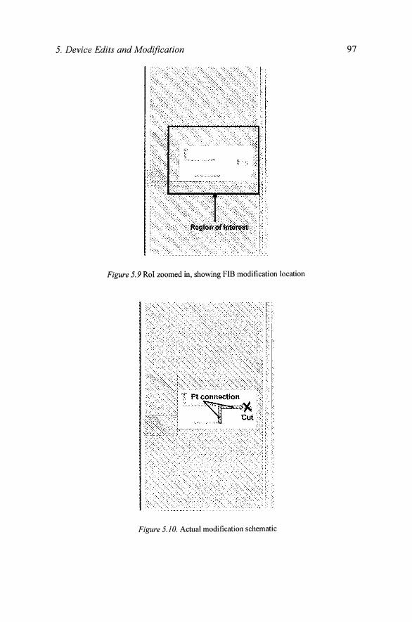
This is just what the name implies, when you use visual references to reach your target location. Top-level metal plots are essential, and once the location is identified on paper, the rest is relatively easy. One has to make sure the orientation of the chip is correct and then proceed to the target location. Figures 6-9 show a typical example of dead reckoning navigation on a chip. Figure 6 shows the overall chip with the region of interest (Rol) indicated by a square. Figures 7-8 show the RoI zoomed in further and Figure 9 shows the target location. Figure 10 shows the fixes involved.
Figure 5.6. Overall chip plot, showing region of interest.

Chapter 5
Figure 5.7. RoI zoomed in
Figure 5.8. RoI zoomed in further
5. Device Edits and Modzfication
Figure 5.9 Rol zoomed in, showing FIB modification location
Figure 5.10. Actual modification schematic

Chapter 5
1.2.2.2.2 3-Point Alignment:
The next level of progression in navigation is using three-point alignment. This is where the stage of the FIB system is realigned using the co-ordinates from the chip obtained from the chip database. This is usually with the chip center as the origin. Stage alignment software on the FIB system allows one to enter the co-ordinates of the three edges of the chip. Once the alignment is complete the stage is aligned to the user-defined units, hence one can navigate by entering the co-ordinates of the target location. One suggestion for the alignment would be to get the co-ordinates for all four corners of the chip. Enter the three points as required, then enter the remaining point to gauge the accuracy of the alignment. Stage offsets would be noticed and corrected at this point. Also the corners are near the bond pads and charge dissipation is better there. With charge dissipation better near the bond pads, imaging is easier and subsequently, chip damage due to the charged beam is minimized.
The same chip is used to illustrate the 3-pt navigation in the figures below. Figure 11 is an overall plot of the chip with the corners marked. A chip schematic is necessary in order to orient the chip prior to alignment. One can use a company logo or a "pin 1" notification on the package for orientation. In this case, box 1 corresponds to the lower left corner of the chip. The corners are zoomed into in Figure 12, as shown. These are mask alignment marks and are oriented this way before the alignment procedure. They are similar on the other corners also. These marks were used because they were there and were convenient, but other references i.e. top level metal features (in each corner) may be used to achieve the same results. One would have to use the design layout to correlate with features on the chip. Figure 13 shows the target location and fixes involved.

5. Device Edits and M o d ~ c a t i o n
n
u
Figure 5.11. Overall chip plot, showing comers for 3-pt alignment
Corner I (Lower left)
Figure 5.12. Corner 1, zoomed in

Chapter 5
Figure 5.13. Schematic of modification, with connections and cut marked.
1.2.2.2.3 CAD Navigation:
The next natural step up for efficient on-chip navigation is using the database information for the layout of the chip. This can be obtained as a .gds file. This information is then converted using the x-y mask information on the different layer structures for the chip. The conversion is typically done on a separate, dedicated workstationIPC, and there is typically an interface between the CAD computer and the FIB system. Different FIB systems use a variety of vendors to convert the information on the .gds files into tangible information for the FIB stage to facilitate on chip navigation. Once the conversions are carried out, the stage is aligned to the CAD navigation software using the 3-pt alignment mentioned above. One important point worth mentioning here, is the fact that, as one aligns the stage and database one has to make sure that the deposition and etch needles do not interfere with the bond pads or wires on their way in and out on the chip. This is especially critical when the FIB locations are near or around the bond pads. Of course, one should be aware of this information from the

5. Device Edits and Modijication 101
earlier planning stage, when the locations are appraised on paper. The database software usually allows the database information to be rotated as needed, so the needles have an easy in and out path.
It would thus suffice to say that one would essentially study the plots, be aware of the FIB locations, check the path of the etch and deposition needles, and then align the CAD information from the database. All this can be checked when the eucentric adjustments are made on the FIB system.
Once the CAD system is aligned to the FIB stage, one can go to the target location either by entering co-ordinates, or by navigating using the CAD software. Once the target area is reached, out come the zoomed-in plots. Also, the different layers can be highlighted on the CAD software. At this point, in today's highly planarized chips, one can hope to find a top-level metal structure, which can be used to fine-tune the alignment. (Van Doorselear, 1993) Typically one uses alignment marks which are similar to the ones mentioned in the previous section, and then proceeds to the target location.
One important point at this juncture is the fact that after the alignment is done, and the target area is arrived at, and the point of contact is determined, one has to typically use an enhanced etch gas for efficient milling. Unfortunately, there is always an image shift when the etch needle is inserted just above the chip. That may be enough to be milling in the wrong place. One way out of this predicament is to define the mill box, as needed, and lightly mill the surface of the chip, so as to make a small indentation on the surface. In this way when the needle is inserted, and image shift occurs, one can correct the location of the mill box using the indentation created as mentioned earlier.
Another unfortunate outcome of planarization is the fact that more often than not, one has to make some "seeker" holes to align with underlying and buried targets. Coupled with the extremely accurate stages provided by the FIB manufacturers, one should be able to reach underlying targets with relative ease. Depending upon how far the seeker holes are one may need to fill them in using FIB induced insulator deposition to avoid unwanted shorting of metals. It is hereby left to the FIB engineer to use whatever means available at hislher disposal to hit underlying metal targets.
1.2.3 Milling vias:
Vias are typically milled using the same beam current used to image the sample. Beam currents between 30-50pA work well for a majority of samples. Vias for top-level metal connections can be just a couple of microns on the side. However, as one needs to make vias on lower level

102 Chapter 5
metals, via size needs to increase. This is because of the higher aspect ratio of the holes, and the fact that when one deposits metal in the vias for making contact, there are chances that the metal bridges on the top of the via instead of making contact with the metal at the bottom. Also larger contact areas ensure lower contact resistance. One can increase the area by making via shapes rectangular instead of being square.
Vias were made in the earlier times using just the regular mill using just the Ga beam. Over time, gas chemistries have enhanced the milling rates for specific materials. The enhanced etch gas used to assist the milling of oxides enhances the milling rate about 7-9 times. What the gas does is essentially convert the sputtered material into a volatile compound, which is pumped away by the vacuum system. This ensures that the via hole is made with minimal redeposition, and the beam is on for a shorter time. It is also a good idea to watch a real time monitor (RTM), update box etc. to check for drift, and also to ascertain when one hits metal. Using end point detection is also highly recommended. (Beam-It; Ashmore; Walker)
1.2.4 Filling vias and making connections with platinum:
1.2.4.1 Filling vias:
Filling vias in top-level metal is straightforward. It is just part of the connection. One just has to make sure that the deposition box is smaller than the via dimension. Making fills on lower level vias is a lot trickier. This is so because if one is not careful, improper deposition techniques will lead to "voiding" in the vim. In this case the Platinum bridges across the top of the via and does not make contact to the metal below.
A couple of good rules of thumb regarding via filling are as follows: a) Make the deposition box smaller (in both dimensions, x and y) than the mill box and b) use the 2 112 minute rule. This number was empirically ascertained. (Beam-It) One needs to alter the dimensions of the deposition box (x, y, z) and the beam current so that the time for the deposition is 2 2 % minutes. This combination ensures better filling in the vias. (Beam-It) Some FIB systems have material files for via fills. The material files usually alter the dwell and overlap times, besides dropping the beam current.

5. Device Edits and ModiJication
1.2.4.2 Making connections:
Another suggestion for figuring out the beam current is to calculate the area of the deposition box and multiplying by 2-6 p ~ / p m 2 . These give a ballpark figure for the beam current to be used. Keep in mind that with higher beam currents one needs to use different material files in order to keep ahead of the deposition curve. (Van Doorselear, 1993)
Typical connections run about 10-75 pm long, 1.5-4 pm wide and about a micron to a micron and half thick. (Beam-It; Carlson, 1997) The deposition tracks need to be wider when using higher beam currents (typically > 350pA). (Beam-It; Carlson, 1997) While doing depositions at higher beam currents (>350 PA) it is generally a good idea not to grab too many frames while depositing, so as to minimize over spray. One can check and compensate for drift using a Real Time Monitor, update box etc.
1.2.5 Disconnecting lines and Clean-up:
1.2.5.1 Disconnecting lines:
In order to avoid refilling of cuts with redeposition, lines are cut or disconnected after all depositions are complete, and prior to over spray clean- up (discussed in the following section). Typical beam currents for exposing the lines to be cut are similar to ones used for exposing lines prior to deposition, i.e. 30-50 PA. It is quite tempting at this stage to use a higher beam current in order to get the job done quickly. It is however prudent to maintain control over the cuts and avoid using beam currents greater than 300 PA. One may start exposing underlying metal levels very quickly, when using a higher beam current. Use of insulator and metal enhancing etch gases is highly recommended so as to have cleaner cuts. Knowledge of barrier metal materials is essential so one can use gases to attack the barrier metals and get the cuts done more quickly and cleanly.
1.2.5.2 Clean-up: Clean up is typically required if there are several modifications in close
proximity to each other and only if the Pt deposition over sprays overlap. If the depositions are far enough away and do not overlap, no clean up is necessary.

Chapter 5
Cleanups can be carried out in a couple of ways: I) One can draw individual mill boxes around the deposition paths
and mill them in series or parallel. Alternatively, one can use the outline mill boxes to achieve the same result. In both cases, one needs to be extremely careful so as not to mill too much into the top surface. Monitoring the mill on the RTM and rapidly grabbing frames would ensure knowing when to quit. One needs to stop when the Pt over spray is milled through.
11) One can also do this: Zoom into the sample (typically around 30- 50 KX) extend the enhanced etch needle, start the flow of gas, and start imaging. Soon one will find the over spray separating out, then one can just move using the joystick and carry on the clean up. (Beam-It; Van Doorselear, 1993)
One important point to be remembered during clean up is to make sure that one does not clean up on lines just deposited. That is quite easy to do and one has to be extremely careful not to do that. Figure 14 gives an example of a clean up following a "complex and messy" FIB modification. The thick white lines are the Pt depositions. The lighter white is the over spray and the black lines in between are the clean ups. The four cut locations are also marked. In this case the depositions needed to be isolated from each other, and were successfully carried out as shown.

5. Device Edits and ModiJication 105
Figure 5.14. Complex modification and clean-up
2. SUMMARY:
For future reference, it may be a good idea to design spare gates at top level metals, and also give power and ground contact points at top level metal. These could be scattered all over the top surface, so FIB engineers would not have very far to FIB certain changes that are needed. These would serve two purposes: 1) Provide easy access to tie signals high or low, and 2) Give additional visual reference points to aid navigating in today's planarized multi-layered circuits.
3. ACKNOWLEDGEMENTS
The author would like to acknowledge all his co-workers at Beam-It Inc., during his tenure there for all the discussions, and a lot of experimentation we were encouraged to do, in order to carry out difficult repairs. Also on the list would be folks from FEI Company, Richard Young and Peter Carleson in particular, for helpful advice and useful discussions over the past several years. Credit also goes to Sho Nakahara, Bob Privette, for their constant

106 Chapter 5
support and encouragement, and Judy Moore, Agere Systems, for help with the figures and manuscript. A special mention would also go out to Robert Ashmore, Robert Pajak, and Bruce Griffiths (all from Agere systems) for their contributions and many useful discussions. The original pictures for Figures 6-13 were provided by Clinton Holder, Esq., Agere Systems (and were actual modifications that were carried out), and are gratefully acknowledged. A special mention also to Joe Serpiello and my boss Jim Cargo, Agere Systems, for their help with the final version of the manuscript and comments.
REFERENCES
Ashmore R, Griffiths B, and Pajak R, private discussions of the PAL FIB group, Agere Systems, Allentown, Pa.
Beam-It, Inc., Numerous discussions, experiments and notes compiled during the author's tenure.
Benbrick J, Rolland G, Perdu P, Casari M, Desplats R " Focused Ion Beam Irradiation Induced Damages on CMOS and Bipolar Technologies," Proceedings, ISTFA'98, pp. 49-57 (1998).
Campbell AN and Soden JM, "Voltage Contrast in the FIB as a Failure Analysis Tool", Electronic Failure Analysis desk reference, pp. 129-135 (1998).
Carlson P, "Integrated Circuit Modification", Course notes The Essentials of Focused Ion Beam Technology, University of Maryland, October 5,6, (1997).
Van Doorselear K, Van Den Reeck, Van Den Bempt L, Young R, Whitney J, "How to Make Golden Devices using Lesser Materials", Proceedings ISTFA, pp. 404- 414 (1993).
Walker J, Applications note, "Focused Ion Beam Applications Using Enhanced Etch", FEI Europe, LTD
Wills KS, and S. V. Pabisetty SV, "Microsurgery Technology for the Semiconductor Industry", Electronic Failure Analysis, desk reference, pp.227-276 (1998).
Copyright © 2022 FDOKUMEN