
Physics of Nanostructured Solid State Devices
567
Physics of Nanostructured Solid State Devices
-
Upload
khangminh22 -
Category
Documents
-
view
2 -
download
0
Transcript of Physics of Nanostructured Solid State Devices

Physics of Nanostructured Solid State Devices


Supriyo Bandyopadhyay
Physics of NanostructuredSolid State Devices
123

Supriyo BandyopadhyayDepartment of Electrical and Computer EngineeringVirginia Commonwealth University601 West Main StreetRichmond, VA, USA
ISBN 978-1-4614-1140-6 e-ISBN 978-1-4614-1141-3DOI 10.1007/978-1-4614-1141-3Springer New York Dordrecht Heidelberg London
Library of Congress Control Number: 2012930227
© Springer Science+Business Media, LLC 2012All rights reserved. This work may not be translated or copied in whole or in part without the writtenpermission of the publisher (Springer Science+Business Media, LLC, 233 Spring Street, New York,NY 10013, USA), except for brief excerpts in connection with reviews or scholarly analysis. Use inconnection with any form of information storage and retrieval, electronic adaptation, computer software,or by similar or dissimilar methodology now known or hereafter developed is forbidden.The use in this publication of trade names, trademarks, service marks, and similar terms, even if they arenot identified as such, is not to be taken as an expression of opinion as to whether or not they are subjectto proprietary rights.
Printed on acid-free paper
Springer is part of Springer Science+Business Media (www.springer.com)

Dedicated to the memory of my father


Preface
This textbook is intended to introduce a first year graduate student of electricalengineering and/or applied physics to concepts that are critical to understandingthe behavior of charge carriers (electrons and holes) in modern nanostructuredsolid state devices. The student is assumed to have undergraduate background insolid state physics, solid state devices, and quantum mechanics. Many of the topicsdiscussed here are specific to ultrasmall (nanostructured) devices, but some aremore general and apply to any solid. This material is the result of the author’steaching a graduate level introductory course on electron theory of solids in three USuniversities over a period spanning nearly 25 years. It has been his experience thatonce students are able to grasp the concepts presented here and become comfortablewith them, they are able to handle more difficult and specialized topics quite easily.
This book is organized into nine chapters. The first chapter reviews the steady-state “drift–diffusion model” of charge transport in solids that electrical engineerstypically learn in their first undergraduate solid state device course. Physicsundergraduates are less exposed to this topic, but should be able to grasp theconcept easily. This chapter introduces the basic drift–diffusion model, starting withtwo important assumptions about the nature of charge conduction in solids, andemphasizes the notion that this model is valid only as long as nonlocal transporteffects are absent. It ends with an introduction to the so-called “equations of state”(also known as drift–diffusion equations) that are used to compute the carrierconcentration and current density in a solid state device self-consistently. Onlysteady-state transport is considered.
Chapter 2 discusses a more sophisticated charge transport model based on theBoltzmann Transport Equation (BTE). It derives this equation from conservationprinciples, and then uses it to deduce the generalized moment equation (or thehydrodynamic balance equation) which governs charge transport in the presenceof both local and nonlocal effects. The steady-state drift–diffusion equations ofChap. 1 are shown to be special cases of the last equation. Two methods of solvingthe BTE—the relaxation time approximation and the Monte Carlo (MC) simulationmethod—are discussed and some analytical results are obtained from the relaxationtime approximation. This chapter also discusses linear response transport or ohmic
vii
viii Preface
conduction and finds an expression for the linear response conductivity. It thendistinguishes chemical potential from electrostatic potential inside a device anddiscusses a few important thermodynamic concepts pertinent to charge transport.Overall, the purpose of this chapter is to provide a sound basis for understandingboth linear and nonlinear (or hot-carrier) transport in solids.
Chapter 3 reviews basic concepts in quantum mechanics, operators and theirapplications, energy quantization in quantum-confined systems (i.e., nanostructures)such as quantum wells, wires and dots, and ends with a description of time-independent and time-dependent perturbation theory. The purpose is to present theessential tools needed to understand and appreciate the quantum foundations ofnanostructured solid state devices. As an example of applying quantum mechanicsto a solid state device, time-independent perturbation theory is employed toelucidate the operation of an electro-optic modulator based on the quantum-confinedStark effect. Performance metrics of this device are calculated using perturbationtheory, thereby exemplifying how quantum mechanics plays a critical role in deviceoperation.
Chapter 4 presents methods of calculating the bandstructure (energy versuswavevector relation) of a crystalline solid based on time-independent perturbationtheory. Since bandstructure plays a vital role in the operation of many devices,particularly optical devices, it is included in this book. More importantly, it is onemore application of time-independent perturbation theory to an actual problem. Wediscuss four different bandstructure calculation methods—the nearly-free electronmethod, the orthogonalized plane wave (OPW) expansion method, the tight-bindingapproximation (TBA) and the Ek � Ep theory—three of which invoke time-independentperturbation theory. Band structure results are then applied to calculate the densityof states of electrons and holes as a function of particle energy in bulk (three-dimensional systems) and nanostructured systems such as quantum wells (quasitwo-dimensional) and wires (quasi one-dimensional). Based on the density of states,analytical expression are derived for equilibrium carrier concentrations in three-, two- and one-dimensional structures. This chapter ends with a derivation of thephonon and photon density of states in a crystal.
Chapter 5 illustrates the application of time-dependent perturbation theory totransport physics. It uses this theory to derive Fermi’s Golden Rule which providesa useful prescription to calculate the rate with which an electron scatters as it travelsthrough a solid and interacts with various entities such as impurities and phonons.These rates appear in the BTE and are first mentioned in Chap. 2, but derived here.In order to make the student comfortable in applying Fermi’s Golden Rule to variousproblems, the scattering rate of an electron interacting with nonpolar acousticphonons is derived in three-, two-, and one-dimensional systems as a function ofthe electron’s kinetic energy. Such exercises are extremely instructive and revealimportant physics associated with carrier interactions with the environment inboth bulk- and quantum-confined systems. Once students master the technique ofcalculating the scattering rate due to any one type of interaction, they should beable to calculate the rate associated with any other type of interaction since the

Preface ix
basic principle is the same. A few advanced topics such as phonon confinement andphonon bottleneck effects are also discussed.
Chapter 6 discusses electron–photon interactions and their impact on the opticalproperties of solids, while addressing the general concepts of absorption, sponta-neous emission, and stimulated emission of light. Fermi’s Golden Rule is utilizedto calculate absorption and luminescence intensities as a function of photon energyin three-, two and one-dimensional systems. The basic physics behind the operationof some solid state optical devices, such as light emitting diodes (LED) and lasers,is also discussed. This chapter also discusses excitons since they impact opticalproperties of solids, and could produce nonlinear optical effects. Finally, somespecial topics of current interest in nanophotonics, such as polariton lasers, photoniccrystals, and negative refraction are discussed. This is the only chapter that dealswith “optical properties” of nanostructured solids; the rest are mainly focused on“transport properties.”
Chapter 7 discusses the behavior of an electron in a magnetic field. It firstintroduces the Dirac equation and the Pauli equation to account for an electron’sspin explicitly and then focuses on the “spinless” electron in order to discuss effectsunrelated to the spin. The important concepts of magnetic vector potential and“gauge” are introduced, and the Schrodinger equation is solved in two- and one-dimensional systems to find the wavefunctions and energy eigenstates. Solution ofthe Schrodinger equation in a two-dimensional system leads to the idea of Landaulevel quantization, as well as its observable effects such as Shubnikov–deHaasconductance oscillations. In the context of one-dimensional systems, the conceptof edge states is introduced along with hybrid magneto-electric states. A deviceapplication of the physics, namely the operation of a magneto-optical device basedon quantum-confined Lorentz effect (QCLE) (a magnetic analog of the quantum-confined Stark effect) is discussed. This chapter concludes with a few basic remarksregarding the integer and fractional quantum Hall effect (FQHE).
Chapter 8 introduces some popular quantum transport formalisms such as thescattering matrix formalism, the Landau–Vlasov equation (which can be viewedas a quantum-mechanical equivalent of the collisionless BTE), the nonequilibriumGreen’s function approach, the Wigner distribution function, the Tsu–Esaki formal-ism, and the Landauer–Buttiker approach for linear response transport. Applicationsof these formalisms are presented in Chap. 9.
In Chap. 9, some of the quantum transport formalisms developed in Chap. 8 areapplied to actual quantum devices. The Tsu–Esaki formula is used to calculate thetunneling current in resonant tunneling devices and numerous mesoscopic devicesand phenomena are treated with the Landauer–Buttiker formalism. This chapter isintended to show how quantum mechanics impacts the operation of nanostructureddevices.
The author is grateful to his numerous graduate students who had this course andoften made valuable contributions to developing the course material. There are too

x Preface
many of them to name here. He is also indebted to an anonymous reviewer whomade helpful comments while reviewing the draft.
As always, in spite of the author’s best efforts at proof reading, it is possible thatsome typographical errors have eluded detection. The author will be immenselygrateful if they are brought to his notice by e-mailing him at [email protected].
Welcome to the world of electron physics in nanostructured devices!
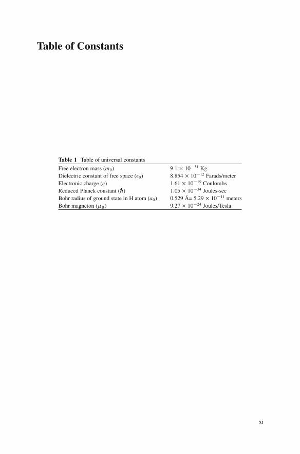
Table of Constants
Table 1 Table of universal constants
Free electron mass (m0) 9.1 � 10�31 Kg.Dielectric constant of free space (�0) 8.854 � 10�12 Farads/meterElectronic charge (e) 1.61 � 10�19 CoulombsReduced Planck constant („) 1.05 � 10�34 Joules-secBohr radius of ground state in H atom (a0) 0.529 A= 5.29 � 10�11 metersBohr magneton (�B) 9.27 � 10�24 Joules/Tesla
xi


Contents
1 Charge and Current in Solids: The Classical Drift–Diffusion Model . . . . . . . . . . . . . . . . . . . . . . . . . . . . . . . . . . . . . . . . . . . . . . . . . . . . . . . . . . . . . . 11.1 Introduction . . . . . . . . . . . . . . . . . . . . . . . . . . . . . . . . . . . . . . . . . . . . . . . . . . . . . . . . . . . . 11.2 Drift–Diffusion Model . . . . . . . . . . . . . . . . . . . . . . . . . . . . . . . . . . . . . . . . . . . . . . . . 41.3 The Drude Model and Ohm’s Law. . . . . . . . . . . . . . . . . . . . . . . . . . . . . . . . . . . . 51.4 Diffusion Current . . . . . . . . . . . . . . . . . . . . . . . . . . . . . . . . . . . . . . . . . . . . . . . . . . . . . . 111.5 Electron and Hole Currents . . . . . . . . . . . . . . . . . . . . . . . . . . . . . . . . . . . . . . . . . . . 131.6 Conservation of Charge and the Continuity Equation . . . . . . . . . . . . . . . 141.7 Determining Transport Variables: The “Equations
of State” or “Drift–Diffusion Equations” .. . . . . . . . . . . . . . . . . . . . . . . . . . . . 161.8 Generation and Recombination Processes . . . . . . . . . . . . . . . . . . . . . . . . . . . . 171.9 Nonlinear but Local Effects: The Drift–Diffusion Model Holds . . . . 201.10 Nonlocal Effects: Invalidity of Drift–Diffusion Model . . . . . . . . . . . . . . 211.11 Summary .. . . . . . . . . . . . . . . . . . . . . . . . . . . . . . . . . . . . . . . . . . . . . . . . . . . . . . . . . . . . . . 27References . . . . . . . . . . . . . . . . . . . . . . . . . . . . . . . . . . . . . . . . . . . . . . . . . . . . . . . . . . . . . . . . . . . . . 33
2 Boltzmann Transport: Beyond the Drift–Diffusion Model . . . . . . . . . . . . . . 352.1 Transport in the Presence of Nonlocal Effects:
The Carrier Distribution Function . . . . . . . . . . . . . . . . . . . . . . . . . . . . . . . . . . . . 352.2 Boltzmann Transport Equation for the Carrier
Distribution Function .. . . . . . . . . . . . . . . . . . . . . . . . . . . . . . . . . . . . . . . . . . . . . . . . . 372.2.1 Limitations of the BTE . . . . . . . . . . . . . . . . . . . . . . . . . . . . . . . . . . . . . . 392.2.2 Limits of Validity of the BTE . . . . . . . . . . . . . . . . . . . . . . . . . . . . . . . 40
2.3 The Generalized Moment Equation or HydrodynamicBalance Equation . . . . . . . . . . . . . . . . . . . . . . . . . . . . . . . . . . . . . . . . . . . . . . . . . . . . . . 41
2.4 Deriving the Drift–Diffusion Equations fromthe Generalized Moment Equation.. . . . . . . . . . . . . . . . . . . . . . . . . . . . . . . . . . . 452.4.1 The Zero-th Moment . . . . . . . . . . . . . . . . . . . . . . . . . . . . . . . . . . . . . . . . . 452.4.2 The First Moment . . . . . . . . . . . . . . . . . . . . . . . . . . . . . . . . . . . . . . . . . . . . 47
2.5 Too Many Unknowns .. . . . . . . . . . . . . . . . . . . . . . . . . . . . . . . . . . . . . . . . . . . . . . . . . 50
xiii

xiv Contents
2.6 Finding the Mobility and Diffusion Coefficient fromthe Carrier Distribution Function . . . . . . . . . . . . . . . . . . . . . . . . . . . . . . . . . . . . . 51
2.7 Methods of Solving the Boltzmann Transport Equation .. . . . . . . . . . . . 582.8 Relaxation Time Approximation Method . . . . . . . . . . . . . . . . . . . . . . . . . . . . 582.9 When Can We Define a Constant Relaxation Time? .. . . . . . . . . . . . . . . . 60
2.9.1 Elastic Scattering. . . . . . . . . . . . . . . . . . . . . . . . . . . . . . . . . . . . . . . . . . . . . 632.9.2 Isotropic Scattering in a Nondegenerate Carrier
Population . . . . . . . . . . . . . . . . . . . . . . . . . . . . . . . . . . . . . . . . . . . . . . . . . . . . 652.10 Low Field Steady-State Conductivity in a Homogeneous
Nondegenerate Electron Gas . . . . . . . . . . . . . . . . . . . . . . . . . . . . . . . . . . . . . . . . . . 662.11 The Monte Carlo Simulation Method for Evaluating
the Distribution Function . . . . . . . . . . . . . . . . . . . . . . . . . . . . . . . . . . . . . . . . . . . . . . 712.11.1 Initial Conditions in the Simulation . . . . . . . . . . . . . . . . . . . . . . . . . 722.11.2 Determination of the Duration of Free Flight. . . . . . . . . . . . . . . 732.11.3 Updating the Electron Trajectory at the End
of Free Flight and Beginning of the Collision Event . . . . . . . 762.11.4 Updating the Electron State After the Collision Event . . . . . 762.11.5 Terminating a Trajectory . . . . . . . . . . . . . . . . . . . . . . . . . . . . . . . . . . . . 782.11.6 Collecting Statistics and Evaluating
the Distribution Function . . . . . . . . . . . . . . . . . . . . . . . . . . . . . . . . . . . . 782.11.7 Finer Points. . . . . . . . . . . . . . . . . . . . . . . . . . . . . . . . . . . . . . . . . . . . . . . . . . . 80
2.12 Summary .. . . . . . . . . . . . . . . . . . . . . . . . . . . . . . . . . . . . . . . . . . . . . . . . . . . . . . . . . . . . . . 81References . . . . . . . . . . . . . . . . . . . . . . . . . . . . . . . . . . . . . . . . . . . . . . . . . . . . . . . . . . . . . . . . . . . . . 89
3 Some Essential Elements of Quantum Mechanics . . . . . . . . . . . . . . . . . . . . . . . . 913.1 Introduction . . . . . . . . . . . . . . . . . . . . . . . . . . . . . . . . . . . . . . . . . . . . . . . . . . . . . . . . . . . . 913.2 The Schrodinger Picture . . . . . . . . . . . . . . . . . . . . . . . . . . . . . . . . . . . . . . . . . . . . . . . 91
3.2.1 Calculating Expectation Values . . . . . . . . . . . . . . . . . . . . . . . . . . . . . 923.3 The Wavefunction and the Schrodinger Equation .. . . . . . . . . . . . . . . . . . . 93
3.3.1 Schrodinger Equation in a Time-Independent Potential . . . 953.3.2 Wavefunction of a Free Electron . . . . . . . . . . . . . . . . . . . . . . . . . . . . 963.3.3 Electron Wave and Electron Waveguide . . . . . . . . . . . . . . . . . . . . 97
3.4 How to Find the Quantum-Mechanical Operatorfor a Physical Quantity . . . . . . . . . . . . . . . . . . . . . . . . . . . . . . . . . . . . . . . . . . . . . . . . 983.4.1 Rectangular Potential Well . . . . . . . . . . . . . . . . . . . . . . . . . . . . . . . . . . 1043.4.2 Parabolic Well . . . . . . . . . . . . . . . . . . . . . . . . . . . . . . . . . . . . . . . . . . . . . . . . 106
3.5 Perturbation Theory . . . . . . . . . . . . . . . . . . . . . . . . . . . . . . . . . . . . . . . . . . . . . . . . . . . 1073.5.1 Time-Independent Perturbation Theory.. . . . . . . . . . . . . . . . . . . . 1083.5.2 Time-Dependent Perturbation Theory . . . . . . . . . . . . . . . . . . . . . . 114
3.6 Wavefunction Engineering: Device Applicationsof Perturbation Theory . . . . . . . . . . . . . . . . . . . . . . . . . . . . . . . . . . . . . . . . . . . . . . . . 1173.6.1 The Velocity Modulation Transistor . . . . . . . . . . . . . . . . . . . . . . . . 1173.6.2 The Electro-Optic Modulator Based
on the Quantum-Confined Stark Effect . . . . . . . . . . . . . . . . . . . . . 119

Contents xv
3.7 Multi-Electron Schrodinger Equation . . . . . . . . . . . . . . . . . . . . . . . . . . . . . . . . 1243.7.1 Hartree and Exchange Potentials . . . . . . . . . . . . . . . . . . . . . . . . . . . . 1283.7.2 Self-Consistent Schrodinger–Poisson Solution .. . . . . . . . . . . . 130
3.8 Summary .. . . . . . . . . . . . . . . . . . . . . . . . . . . . . . . . . . . . . . . . . . . . . . . . . . . . . . . . . . . . . . 133References . . . . . . . . . . . . . . . . . . . . . . . . . . . . . . . . . . . . . . . . . . . . . . . . . . . . . . . . . . . . . . . . . . . . . 145
4 Band Structures of Crystalline Solids . . . . . . . . . . . . . . . . . . . . . . . . . . . . . . . . . . . . . 1474.1 Introduction . . . . . . . . . . . . . . . . . . . . . . . . . . . . . . . . . . . . . . . . . . . . . . . . . . . . . . . . . . . . 1474.2 The Schrodinger Equation in a Crystal . . . . . . . . . . . . . . . . . . . . . . . . . . . . . . . 149
4.2.1 Crystallographic Directions and Miller Indices . . . . . . . . . . . . 1504.3 The Nearly Free Electron Method for Calculating Bandstructure.. . 151
4.3.1 Why Do Energy Gaps Appear in the Bandstructure? . . . . . . 1544.3.2 Designation of Conduction and Valence Bands . . . . . . . . . . . . 155
4.4 The Orthogonalized Plane Wave Expansion Method . . . . . . . . . . . . . . . . 1554.4.1 The Pseudopotential Method . . . . . . . . . . . . . . . . . . . . . . . . . . . . . . . . 159
4.5 The Tight-Binding Approximation Method . . . . . . . . . . . . . . . . . . . . . . . . . . 1604.6 The Ek � Ep Perturbation Method . . . . . . . . . . . . . . . . . . . . . . . . . . . . . . . . . . . . . . . . 165
4.6.1 Application of Perturbation Theory to CalculateBandstructure. . . . . . . . . . . . . . . . . . . . . . . . . . . . . . . . . . . . . . . . . . . . . . . . . 167
4.6.2 A Simple Two-Band Theory: Neglectingthe Remote Bands . . . . . . . . . . . . . . . . . . . . . . . . . . . . . . . . . . . . . . . . . . . . 168
4.6.3 The Effect of Spin–Orbit Interaction on Bandstructure . . . . 1724.6.4 The 8-band Ek � Ep Perturbation Theory . . . . . . . . . . . . . . . . . . . . . . 1754.6.5 The 6�6 Hamiltonian: Neglecting the Split-Off
Valence Band . . . . . . . . . . . . . . . . . . . . . . . . . . . . . . . . . . . . . . . . . . . . . . . . . 1784.6.6 The 4�4 Hamiltonian: Neglecting Spin–Orbit
Interaction . . . . . . . . . . . . . . . . . . . . . . . . . . . . . . . . . . . . . . . . . . . . . . . . . . . . 1794.7 Density of States of Electrons and Holes in a Crystal . . . . . . . . . . . . . . . 184
4.7.1 Equilibrium Electron Concentrationsat Absolute Zero of Temperature . . . . . . . . . . . . . . . . . . . . . . . . . . . . 188
4.7.2 Density of States as a Function of Kinetic Energy . . . . . . . . . 1894.7.3 Calculating the Electron and Hole
Concentrations in a Crystal Using the Densityof States in Kinetic Energy Space . . . . . . . . . . . . . . . . . . . . . . . . . . . 192
4.7.4 Expressions for the Carrier Concentrationsat Nonzero Temperatures . . . . . . . . . . . . . . . . . . . . . . . . . . . . . . . . . . . . 195
4.8 Density of States of Phonons and Photons . . . . . . . . . . . . . . . . . . . . . . . . . . . 1974.8.1 Density of Modes or Density of States of Phonons . . . . . . . . 2004.8.2 Density of States of Photons . . . . . . . . . . . . . . . . . . . . . . . . . . . . . . . . 201
4.9 Summary .. . . . . . . . . . . . . . . . . . . . . . . . . . . . . . . . . . . . . . . . . . . . . . . . . . . . . . . . . . . . . . 202References . . . . . . . . . . . . . . . . . . . . . . . . . . . . . . . . . . . . . . . . . . . . . . . . . . . . . . . . . . . . . . . . . . . . . 207
5 Carrier Scattering in Solids . . . . . . . . . . . . . . . . . . . . . . . . . . . . . . . . . . . . . . . . . . . . . . . . . 2095.1 Charge Carrier Scattering . . . . . . . . . . . . . . . . . . . . . . . . . . . . . . . . . . . . . . . . . . . . . 209

xvi Contents
5.2 Fermi’s Golden Rule for Calculating Carrier Scattering Rates . . . . . . 2095.2.1 Derivation of Fermi’s Golden Rule . . . . . . . . . . . . . . . . . . . . . . . . . 210
5.3 Dressed Electron States and Second Quantization Operators . . . . . . . 2165.3.1 Matrix Elements with Dressed States . . . . . . . . . . . . . . . . . . . . . . . 218
5.4 Applying Fermi’s Golden Rule to Calculate PhononScattering Rates . . . . . . . . . . . . . . . . . . . . . . . . . . . . . . . . . . . . . . . . . . . . . . . . . . . . . . . . 2195.4.1 Einstein’s Thermodynamic Balance Argument .. . . . . . . . . . . . 221
5.5 Calculation of Relaxation Rates . . . . . . . . . . . . . . . . . . . . . . . . . . . . . . . . . . . . . . 2285.5.1 Scattering Rates in 3-D (Bulk) Systems . . . . . . . . . . . . . . . . . . . . 2285.5.2 Scattering Rates in 2-D (Quantum Well) Systems . . . . . . . . . 2375.5.3 Scattering Rates in 1-D (Quantum Wire) Systems . . . . . . . . . 242
5.6 Advanced Topics. . . . . . . . . . . . . . . . . . . . . . . . . . . . . . . . . . . . . . . . . . . . . . . . . . . . . . . 2465.6.1 Phonon Confinement Effects . . . . . . . . . . . . . . . . . . . . . . . . . . . . . . . . 2465.6.2 Phonon Bottleneck Effects . . . . . . . . . . . . . . . . . . . . . . . . . . . . . . . . . . 249
5.7 Summary .. . . . . . . . . . . . . . . . . . . . . . . . . . . . . . . . . . . . . . . . . . . . . . . . . . . . . . . . . . . . . . 250References . . . . . . . . . . . . . . . . . . . . . . . . . . . . . . . . . . . . . . . . . . . . . . . . . . . . . . . . . . . . . . . . . . . . . 254
6 Optical Properties of Solids . . . . . . . . . . . . . . . . . . . . . . . . . . . . . . . . . . . . . . . . . . . . . . . . . 2576.1 Interaction of Light with Matter: Absorption
and Emission Processes . . . . . . . . . . . . . . . . . . . . . . . . . . . . . . . . . . . . . . . . . . . . . . . 2576.1.1 The k-selection Rule . . . . . . . . . . . . . . . . . . . . . . . . . . . . . . . . . . . . . . . . . 2606.1.2 Optical Processes in Direct-Gap and Indirect-
Gap Semiconductors .. . . . . . . . . . . . . . . . . . . . . . . . . . . . . . . . . . . . . . . . 2646.2 Rate Equation in Two-Level Systems. . . . . . . . . . . . . . . . . . . . . . . . . . . . . . . . . 265
6.2.1 Gain Medium and Lasing . . . . . . . . . . . . . . . . . . . . . . . . . . . . . . . . . . . . 2696.3 The Three Important Optical Processes . . . . . . . . . . . . . . . . . . . . . . . . . . . . . . 2706.4 Van Roosbroeck–Shockley Relation . . . . . . . . . . . . . . . . . . . . . . . . . . . . . . . . . . 273
6.4.1 The B-Coefficient . . . . . . . . . . . . . . . . . . . . . . . . . . . . . . . . . . . . . . . . . . . . 2766.5 Semiconductor Lasers . . . . . . . . . . . . . . . . . . . . . . . . . . . . . . . . . . . . . . . . . . . . . . . . . 276
6.5.1 Threshold Condition for Lasing . . . . . . . . . . . . . . . . . . . . . . . . . . . . . 2776.6 Different Types of Semiconductor Lasers . . . . . . . . . . . . . . . . . . . . . . . . . . . . 282
6.6.1 Double Heterostructure Lasers . . . . . . . . . . . . . . . . . . . . . . . . . . . . . . 2836.6.2 Quantum Well Lasers . . . . . . . . . . . . . . . . . . . . . . . . . . . . . . . . . . . . . . . . 2836.6.3 Quantum Cascade Lasers . . . . . . . . . . . . . . . . . . . . . . . . . . . . . . . . . . . . 2836.6.4 Graded Index Separate Confinement
Heterostructure Lasers . . . . . . . . . . . . . . . . . . . . . . . . . . . . . . . . . . . . . . . 2856.6.5 Distributed Feedback Lasers . . . . . . . . . . . . . . . . . . . . . . . . . . . . . . . . 2866.6.6 Vertical Cavity Surface Emitting Lasers . . . . . . . . . . . . . . . . . . . . 2876.6.7 Quantum Dot Lasers . . . . . . . . . . . . . . . . . . . . . . . . . . . . . . . . . . . . . . . . . 287
6.7 Calculation of K Op;!l .m; n/ in Bulk Semiconductor .. . . . . . . . . . . . . . . . . 2896.7.1 The Electron–Photon Interaction Hamiltonian . . . . . . . . . . . . . 2936.7.2 Polarization Dependence of Absorption and Emission . . . . 298
6.8 Absorption and Emission in SemiconductorNanostructures (Quantum Wells and Wires) . . . . . . . . . . . . . . . . . . . . . . . . . 300

Contents xvii
6.8.1 Quantum Wells . . . . . . . . . . . . . . . . . . . . . . . . . . . . . . . . . . . . . . . . . . . . . . . 3016.8.2 Quantum Wires. . . . . . . . . . . . . . . . . . . . . . . . . . . . . . . . . . . . . . . . . . . . . . . 309
6.9 Excitons . . . . . . . . . . . . . . . . . . . . . . . . . . . . . . . . . . . . . . . . . . . . . . . . . . . . . . . . . . . . . . . . 3146.9.1 Excitons in Quantum-Confined Nanostructures . . . . . . . . . . . . 3186.9.2 Bleaching of Exciton Absorption: Nonlinear
Optical Properties . . . . . . . . . . . . . . . . . . . . . . . . . . . . . . . . . . . . . . . . . . . . 3206.10 Polariton Laser . . . . . . . . . . . . . . . . . . . . . . . . . . . . . . . . . . . . . . . . . . . . . . . . . . . . . . . . . 3216.11 Photonic Crystals . . . . . . . . . . . . . . . . . . . . . . . . . . . . . . . . . . . . . . . . . . . . . . . . . . . . . . 3236.12 Negative Refraction.. . . . . . . . . . . . . . . . . . . . . . . . . . . . . . . . . . . . . . . . . . . . . . . . . . . 325
6.12.1 Superlens . . . . . . . . . . . . . . . . . . . . . . . . . . . . . . . . . . . . . . . . . . . . . . . . . . . . . 3266.12.2 Invisibility Cloaking . . . . . . . . . . . . . . . . . . . . . . . . . . . . . . . . . . . . . . . . . 327
6.13 Summary .. . . . . . . . . . . . . . . . . . . . . . . . . . . . . . . . . . . . . . . . . . . . . . . . . . . . . . . . . . . . . . 328References . . . . . . . . . . . . . . . . . . . . . . . . . . . . . . . . . . . . . . . . . . . . . . . . . . . . . . . . . . . . . . . . . . . . . 339
7 Magnetic Field Effects in a Nanostructured Device . . . . . . . . . . . . . . . . . . . . . . 3417.1 Electrons in a Magnetic Field . . . . . . . . . . . . . . . . . . . . . . . . . . . . . . . . . . . . . . . . . 3417.2 Dirac’s Equation and Pauli’s Equation . . . . . . . . . . . . . . . . . . . . . . . . . . . . . . . 3427.3 The “Spinless” Electron in a Magnetic Field . . . . . . . . . . . . . . . . . . . . . . . . . 3457.4 An Electron in a Two-Dimensional Electron Gas
(Quantum Well) Placed in a Static and UniformMagnetic Field . . . . . . . . . . . . . . . . . . . . . . . . . . . . . . . . . . . . . . . . . . . . . . . . . . . . . . . . . 3457.4.1 Landau Levels and Landau Orbits . . . . . . . . . . . . . . . . . . . . . . . . . . 3497.4.2 Density of States in a Two-Dimensional
Electron Gas in a Perpendicular Magnetic Field . . . . . . . . . . . 3557.4.3 Shubnikov–deHaas Oscillations in a Two-
Dimensional Electron Gas . . . . . . . . . . . . . . . . . . . . . . . . . . . . . . . . . . . 3587.5 An Electron in a One-Dimensional Electron Gas
(Quantum Wire) Placed in a Static and UniformMagnetic Field . . . . . . . . . . . . . . . . . . . . . . . . . . . . . . . . . . . . . . . . . . . . . . . . . . . . . . . . . 3617.5.1 Quantum Wire with Parabolic Confinement
Potential Along the Width . . . . . . . . . . . . . . . . . . . . . . . . . . . . . . . . . . . 3617.5.2 Quantum Wire with Rectangular Confinement
Potential Along the Width . . . . . . . . . . . . . . . . . . . . . . . . . . . . . . . . . . . 3687.5.3 Edge State Phenomena.. . . . . . . . . . . . . . . . . . . . . . . . . . . . . . . . . . . . . . 3737.5.4 Shubnikov–deHaas Oscillations in a Quasi
One-Dimensional Electron Gas . . . . . . . . . . . . . . . . . . . . . . . . . . . . . 3747.6 The Quantum-Confined Lorentz Effect . . . . . . . . . . . . . . . . . . . . . . . . . . . . . . . 3757.7 The Hall Effect in a Two-Dimensional Electron Gas . . . . . . . . . . . . . . . . 3777.8 The Integer Quantum Hall Effect . . . . . . . . . . . . . . . . . . . . . . . . . . . . . . . . . . . . . 3827.9 The Fractional Quantum Hall Effect . . . . . . . . . . . . . . . . . . . . . . . . . . . . . . . . . . 3827.10 Summary .. . . . . . . . . . . . . . . . . . . . . . . . . . . . . . . . . . . . . . . . . . . . . . . . . . . . . . . . . . . . . . 386References . . . . . . . . . . . . . . . . . . . . . . . . . . . . . . . . . . . . . . . . . . . . . . . . . . . . . . . . . . . . . . . . . . . . . 393

xviii Contents
8 Quantum Transport Formalisms . . . . . . . . . . . . . . . . . . . . . . . . . . . . . . . . . . . . . . . . . . . 3958.1 When Is a Quantum-Mechanical Model for Transport Necessary? . 3958.2 Quantum Mechanical Model to Calculate Transport Variables. . . . . . 400
8.2.1 How to Calculate the Wavefunction.. . . . . . . . . . . . . . . . . . . . . . . . 4028.2.2 The Transmission Matrix Method . . . . . . . . . . . . . . . . . . . . . . . . . . . 4078.2.3 The Scattering Matrix . . . . . . . . . . . . . . . . . . . . . . . . . . . . . . . . . . . . . . . 4098.2.4 Finding the Composite Current Scattering
Matrix of a Disordered Region . . . . . . . . . . . . . . . . . . . . . . . . . . . . . . 4158.2.5 The Scattering Matrix for an Elastic Scatterer . . . . . . . . . . . . . . 4168.2.6 Finding the Coefficients Am;pIm0 ;p0.x/,
Bm;pIm0 ;p0.x/, Cm;pIm0;p0.x/, and Dm;pIm0 ;p0.x/
at Some Location Within the Device . . . . . . . . . . . . . . . . . . . . . . . . 4198.3 The Importance of Evanescent Modes . . . . . . . . . . . . . . . . . . . . . . . . . . . . . . . . 4288.4 Spatially Varying Potential and Self-Consistent Solutions . . . . . . . . . . 4328.5 Terminal Currents. . . . . . . . . . . . . . . . . . . . . . . . . . . . . . . . . . . . . . . . . . . . . . . . . . . . . . 434
8.5.1 A Two-Terminal Device and Tsu–Esaki Equation . . . . . . . . . 4348.5.2 When Is Response Linear? . . . . . . . . . . . . . . . . . . . . . . . . . . . . . . . . . . 4438.5.3 Landauer Formula and Quantized Conductance
of Point Contacts . . . . . . . . . . . . . . . . . . . . . . . . . . . . . . . . . . . . . . . . . . . . . 4468.5.4 The Buttiker Multiprobe Formula .. . . . . . . . . . . . . . . . . . . . . . . . . . 448
8.6 The 2-probe and 4-probe Landauer Formulas . . . . . . . . . . . . . . . . . . . . . . . . 4518.6.1 The Contact Resistance . . . . . . . . . . . . . . . . . . . . . . . . . . . . . . . . . . . . . . 4558.6.2 The Addition Law of Series Resistance . . . . . . . . . . . . . . . . . . . . . 4568.6.3 Computing the Landauer Resistances by
Finding the Transmission Probability Through a Device . . 4588.7 The Landau–Vlasov Equation or the Collisionless
Quantum Boltzmann Transport Equation.. . . . . . . . . . . . . . . . . . . . . . . . . . . . 4598.8 A More Useful Collisionless Boltzmann Transport Equation . . . . . . . 4648.9 Quantum Correlations . . . . . . . . . . . . . . . . . . . . . . . . . . . . . . . . . . . . . . . . . . . . . . . . . 4668.10 Quantum Transport in an Open System with
Device-Contact Coupling and the Self-Energy Potential . . . . . . . . . . . . 4738.10.1 Coupling of a Device to a Single Contact . . . . . . . . . . . . . . . . . . 474
8.11 The Nonequilibrium Green’s Function Formalism.. . . . . . . . . . . . . . . . . . 4788.12 Summary .. . . . . . . . . . . . . . . . . . . . . . . . . . . . . . . . . . . . . . . . . . . . . . . . . . . . . . . . . . . . . . 480References . . . . . . . . . . . . . . . . . . . . . . . . . . . . . . . . . . . . . . . . . . . . . . . . . . . . . . . . . . . . . . . . . . . . . 488
9 Quantum Devices and Mesoscopic Phenomena . . . . . . . . . . . . . . . . . . . . . . . . . . 4919.1 Introduction . . . . . . . . . . . . . . . . . . . . . . . . . . . . . . . . . . . . . . . . . . . . . . . . . . . . . . . . . . . . 4919.2 Double Barrier Resonant Tunneling Diodes. . . . . . . . . . . . . . . . . . . . . . . . . . 491
9.2.1 Current–Voltage Characteristic of a DoubleBarrier Resonant Tunneling Diode . . . . . . . . . . . . . . . . . . . . . . . . . . 499
9.2.2 Space Charge Effects and Self-Consistent Solution . . . . . . . . 4999.2.3 The Effect of Nonidealities on the
Double-Barrier Resonant Tunneling Diode . . . . . . . . . . . . . . . . . 500

Contents xix
9.2.4 Other Mechanisms for Negative DifferentialResistance in a DBRTD. . . . . . . . . . . . . . . . . . . . . . . . . . . . . . . . . . . . . . 502
9.2.5 Tunneling Time . . . . . . . . . . . . . . . . . . . . . . . . . . . . . . . . . . . . . . . . . . . . . . 5039.3 The Stub-Tuned Transistor . . . . . . . . . . . . . . . . . . . . . . . . . . . . . . . . . . . . . . . . . . . . 5059.4 Aharonov–Bohm Quantum Interferometric Devices. . . . . . . . . . . . . . . . . 509
9.4.1 The Altshuler–Aronov–Spivak Effect . . . . . . . . . . . . . . . . . . . . . . . 5129.4.2 More on the Ballistic Aharonov–Bohm
Conductance Oscillations . . . . . . . . . . . . . . . . . . . . . . . . . . . . . . . . . . . . 5169.4.3 Magnetostatic Aharonov–Bohm Effect in
Quantum Wire Rings . . . . . . . . . . . . . . . . . . . . . . . . . . . . . . . . . . . . . . . . 5179.5 The Electrostatic Aharonov–Bohm Effect . . . . . . . . . . . . . . . . . . . . . . . . . . . . 520
9.5.1 The Effect of Multiple Reflections . . . . . . . . . . . . . . . . . . . . . . . . . . 5249.6 Mesoscopic Phenomena: Applications of Buttiker’s
Multiprobe Formula . . . . . . . . . . . . . . . . . . . . . . . . . . . . . . . . . . . . . . . . . . . . . . . . . . . 5309.6.1 Hall Resistance of a Cross and Quenching of
Hall Resistance . . . . . . . . . . . . . . . . . . . . . . . . . . . . . . . . . . . . . . . . . . . . . . . 5319.6.2 Bend Resistance of a Cross . . . . . . . . . . . . . . . . . . . . . . . . . . . . . . . . . . 5359.6.3 An Alternate Explanation of the Integer
Quantum Hall Effect . . . . . . . . . . . . . . . . . . . . . . . . . . . . . . . . . . . . . . . . . 5359.7 Summary .. . . . . . . . . . . . . . . . . . . . . . . . . . . . . . . . . . . . . . . . . . . . . . . . . . . . . . . . . . . . . . 540References . . . . . . . . . . . . . . . . . . . . . . . . . . . . . . . . . . . . . . . . . . . . . . . . . . . . . . . . . . . . . . . . . . . . . 545
Index . . . . . . . . . . . . . . . . . . . . . . . . . . . . . . . . . . . . . . . . . . . . . . . . . . . . . . . . . . . . . . . . . . . . . . . . . . . . . . . 547


Chapter 1Charge and Current in Solids: The ClassicalDrift–Diffusion Model
1.1 Introduction
All solid state devices, including those that have nanoscale dimensions, can bebroadly classified into two main categories: (1) transport devices where transportof electric charge (resulting in current flow) takes place and is responsible for thedevice’s operation, and (2) optical devices where transport of charge may or maynot take place, but such transport, if present, is not primarily responsible for deviceaction. Instead, what governs device behavior is transition of charge from one energystate to another resulting in the emission or absorption of light or photons. Anexample of the first class of devices is the ubiquitous complementary metal oxidesemiconductor (CMOS) transistor, while an example of the second class of devicesis a semiconductor light emitting diode. Both classes play important roles in ourlives.
This book is primarily concerned with the electron theory of solids that under-girds the operation of the first class of devices, namely transport devices, althoughwe will also have occasion to delve into the second class of devices in onechapter. Needless to say, the operation of transport devices is governed by thephysics of charge transport in solids. Therefore, to understand their operation at thefundamental level, we have to understand how charge transport takes place within asolid, typically a semiconductor. Over the years, increasingly sophisticated modelsof charge transport have been developed. This was necessitated by the decreasingsize of devices; smaller devices need more sophisticated models. As a result, ahierarchy of charge transport models has emerged, which is broadly as follows:
• Drift–diffusion model: It is the easiest to understand and historically the mostwidely used. Its shortcoming is that it cannot capture so-called nonlocal transporteffects that frequently occur in submicron (nanoscale) devices, heterostructureddevices, and devices with strong doping modulation. Within such devices, theelectric field that drives charge transport may change very rapidly in space,resulting in “nonlocality” whereby the behavior of a charge carrier at any locationin the device not only depends on its local surroundings but also on events
S. Bandyopadhyay, Physics of Nanostructured Solid State Devices,DOI 10.1007/978-1-4614-1141-3 1, © Springer Science+Business Media, LLC 2012
1

2 1 Charge and Current in Solids: The Classical Drift–Diffusion Model
taking place at remote sites. In other words, the behaviors at different locationswithin the device are interconnected. Such nonlocal behavior is beyond the drift–diffusion model.
• Boltzmann transport model: This is more sophisticated than the drift–diffusionmodel since it can handle nonlocal transport effects. However, it cannot capturequantum mechanical effects, such as those arising from the interference ofelectron waves. These effects sometimes manifest themselves in ultrasmalldevices at low temperatures and is at the heart of “quantum devices” such asresonant tunneling diodes, whose operations are based on quantum-mechanicalprinciples. As long as such effects are absent, the Boltzmann Transport modelis applicable and therefore it is widely used to model charge transport innanostructured devices at room temperature.
• Quantum transport models: This is the most sophisticated and the most powerfulof all models since it can handle both classical and quantum-mechanical trans-port, but unfortunately it is also the most difficult. Unlike the previous two modelswhich are purely classical and treat charge carriers as classical particles, quantumtransport models account for the quantum-mechanical wave nature of chargecarriers. The wave nature is manifested whenever a device’s critical dimensionsare smaller than the distance an electron can travel before losing quantum-mechanical phase coherence. Today, many nanostructured devices call for a fullquantum-mechanical treatment. They exhibit effects such as current modulationarising from interference of electron waves, which cannot be modeled with anyclassical prescription.
The drift–diffusion model, which is the subject of this chapter, is predicated ontwo basic assumptions about the nature of charge carriers in a solid. They are:
1. Assumption 1: Charge carriers (electrons and holes) are classical particles, likebilliard balls, that travel through a solid obeying the classical Newton’s laws ofmotion.1
2. Assumption 2: While traveling in a solid, charge carriers are subjected to forcesdue to external electric and/or magnetic fields, as well as instantaneous forcesdue to scattering. The latter tend to restore equilibrium of the charge carrierswith their local surroundings.2 The electric and magnetic fields are assumed tovary slowly enough in time and space that a carrier scatters many times beforethese fields change significantly. As a result, a carrier always remains at localequilibrium with its surroundings and its behavior is determined solely by localconditions.
If both these assumptions hold, then the drift–diffusion model is adequate todescribe charge transport in a solid. However, if there are rapid doping and/or
1Relativistic effects that are beyond Newton’s laws are typically unimportant in most solid statedevices since charge carriers travel in them with speeds much less than the speed of light in vacuum.2This is local equilibrium which is different from global equilibrium. Under global equilibriumconditions, no current flows through the solid.

1.1 Introduction 3
compositional variations within a device (e.g., in a heterostructure), then the internalelectric fields can change very quickly in space. In that case, assumption 2 may beviolated. This assumption is also violated if the device is so small (smaller thanthe mean free path of carriers) that a carrier can traverse the entire device withoutsuffering too many collisions with other carriers, impurities or the vibrating atomiclattice (phonons). This type of transport is called nearly collisionless (or “quasi-ballistic”) transport. Since there is not enough scattering to restore local equilibriumfor the carrier, assumption 2 can be violated. When this happens, nonlocal effects aremanifested in the behavior of charge carriers and these effects cannot be capturedwithin the drift–diffusion model. We will see an example of this in the next chapter.
Finally, at very low temperatures and in very small devices, even assumption 1may be violated. When the device dimension is smaller than the inelastic mean freepath of carriers at the operating temperature, a carrier can traverse the entire devicewithout suffering a single inelastic scattering event.3 Inelastic scattering eventsdestroy the quantum-mechanical wave nature of carriers, so that when they areabsent, the wave nature is preserved and carriers can no longer be treated as classicalparticles obeying Newton’s laws. Instead, they must be treated as waves propagatingthrough the device according to the laws of quantum mechanics (Schrodingerequation). Since the inelastic mean free path increases rapidly with decreasingtemperature in most solids, this scenario is quite likely to occur in submicron devicesat temperatures of a few Kelvin.
If carriers behave like waves, they can interfere like waves,4 resulting in a hostof “quantum interference effects” that have collectively come to be known as phasecoherent effects or mesoscopic effects. The term “mesoscopic” was coined in theearly 1980s to describe a regime between the truly microscopic (single atoms ormolecules) and macroscopic. Devices of mesoscopic size will have dimensionscomparable to the so-called “phase breaking length” of carriers, which is thedistance a carrier can travel before phase randomizing collisions randomize anelectron wave’s phase and restore the electron’s classical particle nature. Onlyinelastic collisions randomize the phase; elastic collisions do not. Therefore, thephase-breaking length is basically the inelastic mean free path. The inelastic meanfree path depends on many parameters, such as the ambient temperature, materialpurity, electron concentration, spin orbit interaction in the material, etc., but underfavorable conditions (i.e., at low enough temperatures), it can be longer than 1 �min high-purity semiconductors. Hence, mesoscopic effects are not that rare! In themesoscopic or phase coherent regime of charge transport, neither drift diffusion nor
3The inelastic mean free path is usually longer than the elastic mean free path at low temperatures.A carrier can traverse a device without suffering inelastic collisions, but may suffer elasticcollisions. Such a carrier is still capable of manifesting quantum-mechanical interference effectssince its phase has not been randomized.4An electron can interfere only with itself; two different Fermi particles do not interfere witheach other. However, an electron interfering with itself can result in observable effects that cannotbe captured by the drift–diffusion model or the Boltzmann transport model, and will require fullapplication of quantum transport models.

4 1 Charge and Current in Solids: The Classical Drift–Diffusion Model
Device larger than both elastic andinelastic mean free path and electricfield changes little within a meanfree path
DRIFT-DIFFUSION MODELADEQUATE
Device larger than both elastic andinelastic mean free path but electricfield changes significantly within amean free path
DRIFT-DIFFUSION MODELINADEQUATE; BOLTZMANNTRANSPORT MODEL REQUIRED
Device smaller than inelastic meanfree path
DRIFT-DIFFUSION MODEL ANDBOLTZMANN TRANSPORT MODELINADEQUATE; QUANTUMTRANSPORT MODELS REQUIRED
Fig. 1.1 Validity regimes forthree different transportmodels
Boltzmann transport models have any validity since they are both based on classicalphysics and cannot describe quantum-mechanical effects. In this regime, the onlyreliable recourse will be the quantum transport models.
The validity regimes for different transport models are indicated in Fig. 1.1.In the remainder of this chapter, we will discuss the drift–diffusion model.
Graduate students or senior undergraduate students with some background in solidstate devices, physics and/or materials, are probably already familiar with theessential elements. We revisit them below.
1.2 Drift–Diffusion Model
In the drift–diffusion model, electric current in a solid is viewed as being the resultof two effects: (1) electrons (and/or holes) drifting under an applied electric field(caused by an applied voltage across the device), and (2) the same particles diffusing

1.3 The Drude Model and Ohm’s Law 5
from a region of higher concentration to a region of lower concentration as a resultof interparticle collisions. These two phenomena—drift and diffusion—are solelyresponsible for current flow. Hence the name “drift–diffusion model.”
We just mentioned that drift is caused by an applied electric field, but thisimmediately raises a question. The term “drift” usually implies that the chargecarriers are moving or drifting with a constant velocity. But why should the velocitybe constant in an electric field? After all, the electric field results in a force onthe electron equal in magnitude to the product of the electron’s charge and thestrength of the electric field. This force should accelerate the electron, causingits velocity to increase continuously with time. So, how does the electron reacha constant “drift velocity?” It happens because there are other forces that act on theelectron in a solid. The electron typically collides with other electrons, impurities,and even the vibrating atoms in the solid (phonons), which slows it down. In theend, these scattering forces act like a frictional force whose magnitude is roughlyproportional to the electron’s velocity. The frictional force always opposes the forcedue to the accelerating electric field. When these two forces exactly balance, thenet acceleration vanishes and the electron reaches a steady-state velocity and beginsto “drift.” This picture is sometimes referred to as the Drude model in solid statephysics.
Diffusion, on the other hand, is a more complicated issue. It has its origin ininterparticle collisions which has the net effect of driving charge carriers from aregion of higher concentration to one of lower concentration, resulting in currentflow. However, it is more complicated because diffusion is not a single particleconcept. Hence, it cannot be derived from simple Newton’s laws. Many particlesare required to make up a “concentration” and collisions between them drivediffusion. Hence, diffusion is inherently a multiparticle concept. We will examinethe implication of this later in this chapter.
1.3 The Drude Model and Ohm’s Law
We mentioned at the outset that the drift–diffusion model is predicated on twoassumptions, namely (1) charge carriers are classical particles that obey Newton’slaws, and (2) they scatter many times in a solid before the electric field driving themchanges significantly. Under assumption (2), scattering enforces local equilibrium.Hence, the frictional force due to scattering depends on local conditions alone, suchas the local carrier velocity (Fig. 1.2).
Consider now a single electron that obeys the above two assumptions. Newton’ssecond law (assumption 1) mandates that the electron’s velocity Evn.Er; t/ at positionEr and at the instant of time t obeys the equation
m�n
dEvn.Er; t/
dtD �eŒEE.Er; t/ � Evn.Er; t/ � EB.Er; t/� C Fscat.Er; t/; (1.1)

6 1 Charge and Current in Solids: The Classical Drift–Diffusion Model
distance along the direction of the electric field
Ele
ctric
fiel
d
Electron motion
Fig. 1.2 Pictorial depiction of the conditions under which assumptions 1 and 2 that undergird thedrift–diffusion model are valid. Scattering causes the electron motion to be a random walk. Notethat the carrier scatters many times before the electric field changes appreciably
where EE.Er; t/ is the electric field acting on the electron at position Er at the instantt , and EB.Er; t/ is the magnetic flux density at that position at that instant of time.The electron’s charge is �e and Fscat.Er; t/ is the local scattering force that theelectron experiences at location Er at the instant t . Furthermore, m�.Er; t/ is the localeffective mass of the electron, which, we assume to be time dependent for the sakeof generality.5 In a crystal, (1.1) is not exactly the correct equation for Newton’slaw. In the correct equation, we have to replace m�Ev with the crystal momentum „Ek,where Ek is the electron’s wavevector. At this point however, we will not worry aboutthis subtlety and assume that the two quantities are the same.
Since scattering forces act like frictional forces that damp an electron’s velocity,and since frictional forces are usually proportional to a moving body’s velocity butact in the direction opposite to the velocity, we can write (Drude’s assumption)
Fscat.Er; t/ D �m�nEvn.Er; t/
�n.Er; t/; (1.2)
5The concept of “effective mass” will be discussed in more detail in Chap. 4 when we discussbandstructures of solids. For the time being, suffice it to say that in a crystalline solid, an electronexperiences a periodic electrostatic force because of the periodically placed background ions.This force needs to be accounted for in Newton’s law. Its presence will make matters immenselycomplicated, but fortunately we can get by without accounting for it as long as we replace the realmass of the electron with an effective mass. The effective mass depends on the energy-wavevectorrelation of the electron in the crystal and is generally different from the real mass. The use of theeffective mass also allows us to use Newton’s classical law to describe the motion of an electronin a solid, which, in truth, should be described using quantum-mechanical laws and not Newton’slaws.

1.3 The Drude Model and Ohm’s Law 7
where �n.Er; t/ is the local (instantaneous) time constant associated with relaxationof electron velocity due to scattering. Note that we implicitly invoked assumption(2) when we wrote down the last equation because we assumed that the localfrictional force depends only on the local effective mass, local velocity, and localtime constant. Drude’s assumption is valid only under weak electric fields whenthe acceleration of the electron is small, because only then can the frictional forceinstantaneously adjust to the local velocity.
Let us now restrict ourselves only to steady-state conditions when all variablesbecome time independent. In that case, the derivative with respect to time in (1.1)will vanish6 and we will immediately get (assuming that there is no magnetic field)
Evn.Er/ˇˇsteady-state D �e�n.Er/
m�n
EE.Er/ D ��n.Er/ EE.Er/; (1.3)
where �n.Er/ ( D e�n.Er/=m�n) is the local electron drift mobility.7 Since we restricted
ourselves to steady-state conditions, we dropped the variable t in (1.3). The negativesign in the last equation is a result of the negative charge of the electron. Becauseof this negative sign, the electron velocity is always directed opposite to the electricfield.
Equation (1.3) is the well-known equation of the Drude model of charge con-duction and is the defining equation for drift mobility at low electric field strengthswhen Drude’s assumption holds. At high electric fields, Drude’s assumption willbreak down. Effectively, that will make �n.Er/ depend on EE.Er/, which will makethe relationship between Evn.Er/
ˇˇsteady-state and EE.Er/ nonlinear. When that happens,
the drift mobility will no longer be constant, but will depend on the local electricfield EE.Er/. As long as that is all it depends on, our “local” model will still hold andthe drift–diffusion model will remain valid. However, sometimes the mobility maydepend on other factors that are associated with what is going on at remote locations.If and when that happens—i.e., nonlocal effects take hold—the entire drift–diffusionmodel collapses, as we have stated before. In this chapter, we will not worry aboutsuch situations.
The local electron current density in a solid EJn.Er/ is, by definition, related to theelectron velocity as
EJn.Er/ D �n.Er/eEvn.Er/; (1.4)
where n.Er/ is the local concentration of electrons. The negative sign on the right-hand-side merely reflects the fact that the direction of conventional current (definedas the direction of flow of positive charges) is opposite to the direction of the electronvelocity.
6This happens when the electron is no longer accelerating or decelerating, which means that theexternal and frictional forces exactly balance.7The perceptive reader would notice that we have defined the drift mobility while ignoring anymagnetic field. Therefore, the drift mobility is not a good transport parameter if a magnetic field ispresent.

8 1 Charge and Current in Solids: The Classical Drift–Diffusion Model
We deduce from the last two equations that the steady-state current densitywill be
EJn.Er/ˇˇˇsteady-state
D n.Er/e�n.Er/ EE.Er/ D �n.Er/ EE.Er/; (1.5)
where
�n.Er/ D n.Er/e�n.Er/: (1.6)
Here, we have attached the subscript “n” to the mobility � and the velocity v just toremind us that it is the mobility and velocity of electrons, as opposed to the mobilityand velocity of the other type of charge carriers in a semiconductor (holes). Thequantity �n.Er/ is the local conductivity of electrons. At low electric field strengths,both �n.Er/ and �n.Er/ will be independent of the electric field strength EE.Er/. In thatcase, (1.5) will be nothing but Ohm’s law. Therefore, the Drude model directly givesus Ohm’s law.
Special Topic 1: Hall resistance and longitudinal resistance
Consider the resistor (a rectangular sample) shown in Fig. 1.3. A magnetic field isdirected along the z-direction and an electric field is applied along the x-directionthat causes a current to flow in that direction. Because the magnetic field exerts aLorentz force on the electron in the y-direction, the latter’s trajectory will bend asshown (so that its velocity develops a y-component) and consequently electrons willpile up at one edge of the resistor. This charge “pile up” will cause an electric fieldalong the y-direction, which, in turn can cause a current to flow in the y-direction ifwe electrically connect (or shunt) the two edges of the resistor.
Magnetic field
vx
vy
x
yz
Fig. 1.3 A resistor where amagnetic field is appliedalong the z-direction and anelectron is injected with avelocity along the x-direction

1.3 The Drude Model and Ohm’s Law 9
The steady-state version of (1.1) in this case will be
eŒ EE.Er/ � Evn.Er/ � EB.Er/� D �m�nEvn.Er/
�n.Er/: (1.7)
This vector equation can be written as three scalar equations for the threecomponents of the velocity:
vx.Er/ D �e�n.Er/
m�n
ŒEx.Er/ � vyB.Er/� D ��n.Er/ŒEx.Er/ � vyB.Er/�
vy.Er/ D �e�n.Er/
m�n
ŒEy.Er/ C vxB.Er/� D ��n.Er/ŒEy.Er/ C vxB.Er/�
vz.Er/ D �e�n.Er/
m�n
Ez.Er/ D ��n.Er/Ez.Er/; (1.8)
where
EE.Er/ D Ex.Er/ Ox C Ey.Er/ Oy C Ez.Er/OzEvn.Er/ D vx.Er/ Ox C vy.Er/ Oy C vz.Er/OzEB.Er/ D B.Er/Oz: (1.9)
The first two relations in (1.8) can be combined and written in a matrix form as
"� 1
�n.Er/B.Er/
�B.Er/ � 1
�n.Er/
#�vx.Er/
vy.Er/
�
D�
Ex.Er/
Ey.Er/
�
: (1.10)
Using (1.4), the last equation can be written as2
4
1
�n.Er/�B.Er/
B.Er/ 1�n.Er/
3
5
�Jx.Er/=en.Er/
Jy.Er/=en.Er/
�
D�
Ex.Er/
Ey.Er/
�
: (1.11)
Finally, using (1.6), we can write
1
�n.Er/
�1 ��n.Er/B.Er/
�n.Er/B.Er/ 1
� �Jx.Er/
Jy.Er/
�
D�
Ex.Er/
Ey.Er/
�
: (1.12)
The resistivity tensor Œ�.Er/� is defined as
��xx.Er/ �xy.Er/
�yx.Er/ �yy.Er/
� �Jx.Er/
Jy.Er/
�
D�
Ex.Er/
Ey.Er/
�
; (1.13)

10 1 Charge and Current in Solids: The Classical Drift–Diffusion Model
which yields
�xx.Er/ D �yy.Er/ D 1
�n.Er/
��xy.Er/ D �yx.Er/ D �n
�Er�B.Er/
�n.Er/D B.Er/
en.Er/: (1.14)
The diagonal resistivity (e.g., �xx D Ex=JxjJy D0) is called the longitudinalresistivity, and the off-diagonal resistivity (e.g., �yx D Ey=Jx
ˇˇJy D0
) is called theHall resistivity. The latter is linearly proportional to the magnetic flux density andthe proportionality constant depends only on the electron concentration n.Er/. Hence,measurement of this proportionality constant, called the Hall constant, will allowone to determine the average carrier concentration in the sample. If there are twotypes of carriers in a sample, namely both electrons and holes, then the situationbecomes a little more complicated, but as long as there is only one type of carrier,or there are two types but one is much more numerous than the other, this simplederivation holds. In the latter case, it holds for the majority carriers.
Hall measurement is a routine way of measuring majority carrier concentrationin a sample. The experiment is carried out by measuring the voltage Vy between thetransverse edges of a sample with a voltmeter, while applying a magnetic field in thez-direction and passing a current in the x-direction using a current source. Becausean ideal voltmeter has infinite impedance, it should draw no current so that Jy D 0.The electric field Ey is estimated from the relation Ey D Vy=W , where W is thesample’s width. The current density Jx is measured with an ammeter. All this yieldsthe Hall resistivity �yx D Ey=Jx
ˇˇJy D0
. By measuring this quantity under various
flux densities, one can obtain the Hall constant and from it the carrier concentrationas long as the sample is unipolar (only one type of charge carrier is present) orbipolar (both types of charge carrier are present) but one type is the majoritycarrier.
Note that we can define a conductivity tensor Œ�.Er/� as
��xx.Er/ �xy.Er/
�yx.Er/ �yy.Er/
� �Ex.Er/
Ey.Er/
�
D�
Jx.Er/
Jy.Er/
�
: (1.15)
Since, we should have Œ�.Er/��1 D Œ�.Er/�, we will obtain that
��xx.Er/ �xy.Er/
�yx.Er/ �yy.Er/
�
D2
4
�yy .Er/
�xx.Er/�yy.Er/��xy .Er/�yx.Er/� �yx.Er/
�xx.Er/�yy .Er/��xy .Er/�yx.Er/
� �xy .Er/
�xx.Er/�yy .Er/��xy .Er/�yx.Er/
�xx.Er/
�xx.Er/�yy .Er/��xy .Er/�yx.Er/
3
5: (1.16)
Hence, �xx.Er/ ¤ 1=�xx.Er/, unless the Hall resistances vanish!

1.4 Diffusion Current 11
1.4 Diffusion Current
Ohm’s law relates only the drift current density to the electric field in a solid.It makes no allowance for the diffusion current which does not depend on theelectric field in any case. Ohm’s law could never have accounted for diffusionsince it is based on the Drude model which deals only with a single electron. Asmentioned earlier, diffusion requires multiple electrons to be present. It is caused bya concentration gradient (electrons diffuse from a region with higher concentrationto a region with lower concentration) and a single electron does not define aconcentration. One needs many electrons to form a “concentration.” Therefore,diffusion is a phenomenon that cannot be captured within the single electron pictureand will not emerge from the Drude model.
We have mentioned earlier that diffusion causes particles to move away from aregion of high concentration to a region of low concentration. This happens dueto Brownian motion of particles that causes them to bounce off one another andexecute a random walk. There will be more frequent collisions in the region ofhigh concentration, which will cause the average particle to move toward the lowconcentration region, as shown in Fig. 1.4a. This will happen regardless of whether
Direction of diffusion
λ
a
b
Fig. 1.4 (a) Particles,whether or not they arecharged, diffuse from a regionof higher concentration to aregion of lower concentrationthrough a process of randomwalk. The random walk takesplace since the particlescollide with each other andwith other scatterers presentwithin a solid; (b) A region iscompartmentalized into binsof width � which is the meanfree path. Within each bin, theconcentration is assumed tobe uniform so that theprobability of a particlediffusing to the left is equal tothe probability of diffusing tothe right. The concentration,however, varies from one binto the next

12 1 Charge and Current in Solids: The Classical Drift–Diffusion Model
the particles are charged or uncharged, but if the particles are charged, then the netmotion will result in an electric current. We call this current the “diffusion current.”
In order to derive an expression for the diffusion current, let us consider thesituation in Fig. 1.4b where a sample with nonuniform particle distribution ispartitioned into a number of compartments of equal width �. Here, � is the mean freepath, or the average distance a particle travels before suffering a collision. Although� could be different in different compartments, we will ignore that difference in theensuing zeroth-order analysis.
We will assume that within any compartment, the concentration is approximatelyuniform (although it varies from one compartment to another), so that a particle hasequal probability of moving to the left and to the right. In that case, the number ofelectrons moving from the m-th compartment to the mC1-th compartment in time �
is 12nm�A, where nm is the volume concentration in the m-th compartment, � is the
mean free time between collisions, and A is the cross-sectional area of the sample.Similarly, the number of electrons moving from the mC1-th compartment to them-th compartment in time � is 1
2nmC1�A. The net number crossing the interface
between the two compartments in time � is
nnet D 1
2�AŒnm � nmC1�: (1.17)
The magnitude of the resulting particle flux is
F D nnet
A�D �
2�Œnm � nmC1�: (1.18)
Making a Taylor series expansion of the concentration and retaining only the firstorder term since � is very small, we get
nm � nmC1 D � Errn � E�; (1.19)
where Err is the spatial gradient operator ( Err D .@=@x/ Ox C.@=@y/ Oy C.@=@z/Oz). Thisresults in
EF D � �2
2�Errn D �Dn.Er/ Errn.Er/; (1.20)
where Dn.Er/ is called the (position-dependent) diffusion coefficient. The lastequation is known as Fick’s law.
Clearly, in this simple picture, Dn.Er/ D �2.Er/
2�.Er/. Since both � and � are generally
functions of position within a semiconductor device in steady-state, Dn will be afunction of position as well.
The diffusion current density is the particle flux multiplied by the charge of aparticle. Since the charge of an electron is �e, we can write the current density dueto diffusing electrons as
EJ diffusionn .Er/ D �e EF.Er/ D eDn.Er/ Errn.Er/; (1.21)

1.5 Electron and Hole Currents 13
1.5 Electron and Hole Currents
So far, we have talked mostly about electrons. Let us now turn our attention to holes.Electrons and holes have negative and positive charges, respectively. Therefore,electrons drift in the direction opposite to the electric field and holes drift in thesame direction as the electric field. Consequently, electrons and holes always driftin opposite directions in an electric field. However, since conventional current isviewed as the flow of positive charge, the drift current due to electrons flows inthe direction opposite to the direction in which the electrons are drifting, whereasthe drift current due to holes flows in the same direction as that in which holesare drifting. Therefore, even though electrons and holes drift in opposite directions,their associated drift currents flow in the same direction, namely the direction of theelectric field. Hence, the electron drift current density and hole drift current densityalways have the same sign and they add; they do not subtract. We can write theelectron and hole (steady state) drift currents as
EJn.Er/jdrift D n.Er/e�n.Er/ EE.Er/
EJp.Er/jdrift D p.Er/e�p.Er/ EE.Er/; (1.22)
where n refers to electrons and p to holes. Note that the drift current densities havethe same sign, which is the sign of the electric field. In our convention, the quantitye is always positive; the charge of an electron is �e and the charge of a hole is Ce.
Even though electrons and holes always drift in opposite directions, they neednot diffuse in opposite directions as well. The direction of diffusion is determinedby the direction of the concentration gradient which is a vector quantity. Particles,regardless of whether they are electrons or holes or even charged or uncharged,always diffuse from a region of higher concentration to one of lower concentration.Therefore, they always diffuse in the direction opposite to the concentrationgradient because in going from a region of higher concentration to a region oflower concentration, the gradient is negative. Remembering that the direction ofconventional current is defined as the direction of flow of positive charges, we get
EJn.Er/jdiffusion D eDn.Er/ Errn.Er/
EJp.Er/jdiffusion D �eDp.Er/ Errp.Er/: (1.23)
The total steady-state current density for each type of carrier is obtained byadding the drift and diffusion current densities vectorially. This will yield:
EJn.Er/jsteady-state D n.Er/e�n.Er/ EE.Er/ C eDn.Er/ Errn.Er/
EJp.Er/jsteady-state D p.Er/e�p.Er/ EE.Er/ � eDp.Er/ Errp.Er/: (1.24)

14 1 Charge and Current in Solids: The Classical Drift–Diffusion Model
Electric field
Jndrift
Jpdrift
Jndiffusion
Jpdiffusion
J n
Jp
n
p
J n
Jp
J
Fig. 1.5 The arrows show the directions of the different components of the steady-state electronand hole currents at any given location Er . Note that the drift components are always in the directionof the local electric field. The electron diffusion current component is in the direction of theconcentration gradient for electrons while the hole diffusion current component is directed oppositeto the direction of the hole concentration gradient
Finally, the total steady-state current due to both electrons and holes is given bythe vector sum of the electron and hole currents:
EJ jsteady-state D EJn.Er/jsteady-state C EJp.Er/jsteady-state: (1.25)
In Fig. 1.5, we show pictorially the different steady-state current components thatcan arise in a semiconductor.
1.6 Conservation of Charge and the Continuity Equation
Both electrons and holes, being charged particles, obey the principle of conservationof charge which mandates that charge cannot be created or destroyed arbitrarily.This principle leads to the continuity equation, which we derive below for steady-state situations.

1.6 Conservation of Charge and the Continuity Equation 15
dz
dy
dx
G, RIin
Iout
Fig. 1.6 An incrementalvolume in space wherecurrent is entering and exiting
Consider an incremental region in space with dimensions dx, dy, and dz as shownin Fig. 1.6. Let current flow in the x-direction, with Iin being the current entering thebox and Iout the current exiting.
Therefore, we get that
Iin D Jindydz D dqin
dt
Iout D Joutdydz D dqout
dt; (1.26)
where qin and qout are the charge entering and exiting.In steady state situations, conservation of charge dictates that
qout � qin D qgained � qlost D �gaineddxdydz � �lostdxdydz; (1.27)
where qgained is the charge gained within the box due to generation processes suchas light shining on a semiconductor and creating electron-hole pairs, while qlost isthe charge lost due to electron-hole recombination. Here, � is the charge density.
Combining the last two equations, we obtain
dJ D Jout � Jin D�
�gained � �lost�
dx
dtD�
�gained � �lost�
dx
dt; (1.28)
which yields
dJ
dxD qG � qR; (1.29)
where G is the particle generation rate, R is the particle recombination rate, and q isthe charge of a particle. Remembering that electrons are negatively charged so thatq D �e for them, and holes are positively charged, so that q D e for them, we getthe following continuity equations for electrons and holes in steady state (in threedimensions):
Err � EJn C eGn.Er/ � eRn.Er/ D 0 .for electrons/
Err � EJp � eGp.Er/ C eRp.Er/ D 0 .for holes/: (1.30)

16 1 Charge and Current in Solids: The Classical Drift–Diffusion Model
1.7 Determining Transport Variables: The “Equationsof State” or “Drift–Diffusion Equations”
The utility of any steady-state charge transport model, such as the steady-state drift–diffusion model, is to allow us to determine steady-state transport variables suchas steady-state current density, steady-state carrier concentration, etc. at differentlocations within a solid. If we use the steady-state drift–diffusion model that we havedescribed so far, then we will find the transport variables by solving three differentsets of equations, namely the current equation (one for electrons and one for holes),the continuity equation (again, one for electrons and one for holes) and the Poissonequation. There are a total of five unknowns: EJn.Er/; EJp.Er/; n.Er/; p.Er/; EE.Er/, so thatwe need five equations. These five equations are:
Err � Œ�.Er/ EE.Er/� D eŒp.Er/ � n.Er/� .Poisson equation/
Err � EJn C eGn.Er/ � eRn.Er/ D 0 .electron continuity equation/
EJn.Er/ D n.Er/e�n.Er/ EE.Er/ C eDn.Er/ Errn.Er/ .electron current equation/
Err � EJp � eGp.Er/ C eRp.Er/ D 0 .hole continuity equation/
EJp.Er/ D p.Er/e�p.Er/ EE.Er/ � eDp.Er/ Errp.Er/ .hole current equation/:
(1.31)
Here, Gn.Gp/ and Rn.Rp/ are the generation and recombination rates of electrons(holes). The last five equations are sometimes referred to as the “equations of state,”or simply, “drift–diffusion equations.” They form the basis of the drift–diffusionmodel of steady-state charge transport [5].
The Poisson equation is simply a restatement of the famous Gauss’ law ofelectrostatics. It can be rewritten as
Err � Œ�.Er/ ErrV.Er/� D �� D �eŒp.Er/ � n.Er/�; (1.32)
where the potential V.Er/ is related to the electric field EE.Er/ as
EE.Er/ D � ErrV.Er/: (1.33)
Equation (1.32) is solved subject to the boundary conditions that specify thepotential V.Er/ at two ends of a device. The unknowns p.Er/ and n.Er/ are foundby solving (1.31), (1.33), and (1.32) simultaneously or iteratively. In the iterativeapproach, one starts with a guess for the potential V.Er/ everywhere within thedevice, then extracts the electric field from this potential using (1.33), uses this fieldin (1.31) to find the carrier concentrations, and finally uses those concentrationsin (1.32) to come up with a more refined guess for V.Er/. The process is repeated

1.8 Generation and Recombination Processes 17
until satisfactory convergence is obtained, i.e., until we reach a situation whenˇˇVm.Er/ � Vm�1.Er/
ˇˇ � �, where � is a small voltage, Vm.Er/ is the voltage found
in the m-th iteration and Vm�1.Er/ is the voltage found in the previous iteration. Thismethod of finding the transport variables within a solid state device is sometimescalled self-consistent device analysis.
1.8 Generation and Recombination Processes
In the continuity equations within (1.31), we have two terms G and R associatedwith generation and recombination rates of charge carriers. Electron-hole pairs canbe generated within a solid by external agents such as light shining on the solid,thermal fluctuations, electron bombardment, etc. Additionally, internal processessuch as impact ionization can also generate electron-hole pairs. The number of pairsgenerated per unit time by such processes is the generation rate G. On the otherhand, electron-hole pairs can be annihilated when an electron recombines with ahole while giving off light or heat, or via Auger recombination. The number ofpairs recombining per unit time is the recombination rate R. In both recombinationand generation, net charge is conserved since an electron and a hole have equal butopposite charges. This is consistent with charge conservation. Note that wheneveran electron is generated, a hole is generated as well, and whenever an electron isannihilated, a hole is annihilated with it. Therefore, it is obvious that Gn.Er; t/ DGp.Er; t/.
In light induced generation—also known as “radiative generation”—light isabsorbed in a semiconductor to provide the energy to break a covalent bond betweenatoms and release an electron which becomes free. This process is viewed as aphoton being absorbed to excite an electron from the valence band to the conductionband, leaving behind a hole in the valence band. It is depicted in Fig. 1.7a.
In thermally induced generation, an electron in the valence band absorbs aphonon associated with thermal lattice vibrations and gets excited to a trap levelin the bandgap. Since phonons typically have much less energy than photons, directtransfer from the valence band to the conduction band is usually not possible unlessthe semiconductor has a very small bandgap. The trapped electron may then absorbanother phonon to get to the conduction band. This multiphonon process can exciteelectrons from the valence band to the conduction band in multiple steps and causeelectron–hole pair generation. It is shown in Fig. 1.7b.
Electron–hole pairs can also be generated due to internal processes such asimpact ionization. An electron with large kinetic energy collides with an atom,breaks a bond and knocks off an extra electron leaving behind a hole. In the energyband diagram, this process is viewed as an electron high in the conduction band(large kinetic energy) falling down in the conduction band and the released energyis absorbed to excite an electron from the valence band into the conduction bandleaving behind a hole in the valence band. It is depicted in Fig. 1.7c.

18 1 Charge and Current in Solids: The Classical Drift–Diffusion Model
Ec
Evhole
electron
photon
Eg
Ec
Evhole
electron 2
Eg
electron 1
a c
Ec
Evhole
electron
phonon
Eg
phonon
b
Traplevel
Fig. 1.7 Energy band depictions of generation processes: (a) The process of radiative generationin a semiconductor. A photon is absorbed to excite an electron from the valence band to theconduction band, leaving behind a hole in the valence band. The conduction band edge is denotedby Ec0 and the valence band edge by Ev0. The bandgap is Eg. (b) The process of nonradiativegeneration through the intercession of traps. An electron in the valence band absorbs phonons toreach up to a trap level in the bandgap, leaving behind a hole in the valence band. It then absorbsmore phonons to ultimately reach the conduction band. In the process, an electron–hole pair isgenerated. (c) Process of nonradiative generation via impact ionization. An energetic electron givesup some of its energy, falling down in the conduction band. The released energy is used to excite asecond electron from the valence band to the conduction band, leaving behind a hole in the valenceband. In physical terms, a photon (in process “a”) or a phonon (in process “b”), will provideenough energy to an electron in the outermost (valence) shell of an atom to get free from the atom(ionization). This is depicted as excitation of an electron from the valence to the conduction band,leaving behind a hole in the valence band. In impact ionization, an energetic electron travelingthrough a semiconductor collides with an electron in the outermost shell of an atom and knocks itfree. The first electron loses some of its kinetic energy, but the second electron gets free from itsparent atom. This process is depicted as the first electron falling down in the conduction band andthe second electron getting excited from the valence to the conduction band
Recombination involves an electron and a hole annihilating each other, resultingin the loss of both the electron and the hole. In the energy band diagram, thisprocess is viewed as an electron from the conduction band falling down into thevalence band (in one or multiple steps), releasing energy, and annihilating a hole inthe valence band. The released energy can be given off as light (a photon) or heat(phonons). The former is called radiative recombination and the latter nonradiativerecombination. The radiative processes can be accomplished in a single hop, inwhich case the energy of the photon emitted will be equal to or larger than thebandgap energy. If there are bandgap states, i.e., allowed energy levels in thebandgap of the semiconductor caused by impurities and crystal defects, then it ispossible that the falling electron makes multiple hops, with pit stops at the bandgapstates. Photons may or may not be emitted during any of these hops, but since theenergy difference between the initial and final state of the electron at the beginningand end of a hop is less than the bandgap energy, the energy of the emitted photon(if one is emitted) will be less than the bandgap energy. However, the probability ofa photon being emitted while transitioning through bandgap states is usually verysmall. It is much more likely that phonons are emitted while transitioning throughbandgap states. Since the energy of a phonon in a semiconductor is typically muchless than the bandgap energy, a phonon cannot be usually emitted in the single hop

1.8 Generation and Recombination Processes 19
Ec
Evhole
electron
photon
Eg
Ec
Evhole
electron
phonons
Eg
ba
hole
electron 2
Eg
electron 1
c
Fig. 1.8 Energy band depictions of recombination processes: (a) The process of radiativerecombination in a semiconductor. An electron falls down from the conduction band into thevalence band, releasing a photon, and annihilating itself as well as a hole in the valence band;(b) The process of nonradiative recombination in a semiconductor. An electron falls down fromthe conduction band to the valence band, making stops at bandgap states (shown by dashed lines),and emitting phonons at each step. Ultimately, the electron reaches the valence band where itannihilates itself and a hole; (c) Auger recombination process. Two electrons collide where onegives up its energy to the other. The electron which gains energy goes higher up in the conductionband, while the electron which loses energy falls down into the valence band and annihilates ahole. In physical terms, recombination is the process of an atom capturing a free electron andmaking it quasi-bound. The captured electron settles down into an outer shell of the atom, therebyannihilating a vacancy (hole) there
process. Thus, the presence of bandgap states caused by defects and impuritieshelps the nonradiative (phonon emission) processes, while their absence inhibitsthem. Semiconductor lasers that emit light through the radiative recombinationprocess would prefer that all recombination processes are radiative and none arenonradiative. In fact, the internal quantum efficiency of such a laser is defined asthe ratio of the radiative recombination rate to the total (radiative + nonradiative)recombination rate. Hence, in order to make this efficiency high, the nonradiativeprocesses must be suppressed. This requires eliminating the bandgap states by usingvery pure and perfect semiconductor materials.
Finally, there is one other important process of recombination known as Augerrecombination. Here, two electrons in the conduction band collide. One gains energyfrom the collision and goes high up in the conduction band, while the other losesenergy and drops down into the valence band where it recombines with a hole.In the collision process, the total energy is conserved, i.e., the energy gained byone electron is equal to that lost by the other. Clearly, this process is the converseof impact ionization. Since no light is given off, it is also a form of nonradiativerecombination. Radiative, nonradiative, and Auger recombination processes aredepicted in Fig. 1.8a–c, respectively.
Radiative processes—both recombination and generation—can take place effi-ciently only in so-called “direct-gap” semiconductors like GaAs. They will nothappen efficiently in “indirect-gap semiconductors” like Silicon and Germanium.We will see the reason for that in Chap. 6.

20 1 Charge and Current in Solids: The Classical Drift–Diffusion Model
1.9 Nonlinear but Local Effects: The Drift–DiffusionModel Holds
Equation (1.3) seems to imply that the steady-state drift velocity of carriers inan electric field is linearly proportional to the electric field and the constant ofproportionality is the drift mobility. In reality, the drift mobility may not be aconstant and could depend on the electric field itself, which would make thevelocity versus electric field relation nonlinear. This actually happens in almost allsemiconductors at high enough electric field.
Figure 1.9 shows schematically the magnitude of the steady-state drift velocityversus electric field characteristic in two well-known semiconductors—silicon andGaAs. In both cases, the steady-state drift-velocity is actually proportional to theelectric field at low fields, so that the drift mobility is indeed a field-independentconstant at low field strengths. However, in the case of silicon, the drift velocitysaturates at high field strengths, so that it is no longer proportional to the field and themobility is no longer a field-independent constant. If we still define mobility as theratio of the drift velocity to the electric field, then it becomes progressively smallerwith increasing electric field strength, showing that it is a field-dependent quantity.Consequently, mobility is not a material parameter, since it is not a constant for agiven material. Rather, it is a “transport parameter” indicating how mobile a chargecarrier is in a semiconductor. If the mobility becomes zero, then the drift velocitybecomes zero at any electric field, meaning that the carrier is completely immobileand no amount of force or electric field will make it move. Recall that mobility isproportional to the mean time between collisions and inversely proportional to theeffective mass. Obviously, a particle with infinite effective mass will be immobileand a particle that experiences scattering so frequent that the mean time betweencollisions is zero, will be also effectively immobile. Hence, the term “mobility” forthe quantity � in (1.3) is completely apt.
In the case of GaAs, the drift velocity peaks at a critical electric field and thenactually drops, resulting in a negative slope, or a negative differential mobility. Thisfeature is the basis of the well-known Ridley–Watkins–Hilsum effect or Gunn effect
Electric field Electric field
Car
rier
drift
vel
ocity
Car
rier
drift
vel
ocity
Silicon
GaAsμ1
μ2
E1 E2 E E1 2
μ1
Fig. 1.9 Schematic depiction of the steady-state carrier drift velocity versus electric field charac-teristics in Silicon and GaAs

1.10 Nonlocal Effects: Invalidity of Drift–Diffusion Model 21
[1–3] first observed in GaAs, which is exploited in microwave generators. Here too,the drift mobility will be a function of the electric field strength, since the velocityversus electric-field relation is not linear.
Because of the nonlinearity of the velocity-field characteristics in Fig. 1.9, onemight wonder if the drift–diffusion model can hold up and handle this kind ofnonlinearity. The answer is “yes.” All we have to do is to replace �.Er/ with �. EE.Er//,i.e., the mobility is made a function of the local electric field. This will allow usto model nonlinear effects correctly. We simply have to extract the dependence ofthe mobility on the local electric field using the type of characteristic as shown inFig. 1.9, and use that in determining �. EE.Er//. As long as the drift mobility is afunction of local electric field alone, our drift–diffusion model holds up.
1.10 Nonlocal Effects: Invalidity of Drift–Diffusion Model
The drift–diffusion model will unfortunately crumble if there are nonlocal effects sothat the mobility cannot be expressed as a function of local parameters (such as localelectric field, or local electron energy, etc.) alone. One example of nonlocal effects(in time) is “velocity overshoot” where the velocity of an electron in response to anelectric field exhibits transient behavior. After the electric field is switched on (attime t D 0), the average velocity of the electron ensemble subjected to the electricfield 8 increases rapidly, reaches a peak in time, and then subsides gradually to settledown to the steady-state value as shown in Fig. 1.10. This effect cannot be capturedwithin the drift–diffusion model since the velocity is no longer a unique functionof the local electric field. The final steady-state velocity may be a unique function,but the transient velocity is not. In very short devices, the electron may traversethe entire device without ever reaching steady-state. In such a device, the velocityis never a unique function of the local electric field. Consequently, (1.31) (and theentire drift–diffusion model) will fail in such a device.
Car
rier
velo
city
t1 t2
µ(t1) µ(t2)
time
Fig. 1.10 Velocity overshooteffect. The applied electricfield is constant and turned onat time t D 0. The velocitybegins to rise with time,reaches a peak, and thendrops, ultimately settling to aconstant value
8We call this the “average velocity of the electron ensemble” as opposed to “drift velocity” sinceit is not steady-state.

22 1 Charge and Current in Solids: The Classical Drift–Diffusion Model
r
Leftcontact
Rightcontact
Electric field
Fig. 1.11 A resistor where electrons are injected from the left contact with zero velocity. Theinjected electrons encounter an electric field after entering the resistor (due to the battery), whichpropels them toward the right contact. The electrons may suffer velocity overshoot. The mobilityat location r is not well-defined (it is certainly not uniquely prescribed by the electric field at thatlocation) since it depends on how long it took for electrons to get there. This time depends notonly on the electric field at location r but also on electric fields everywhere to the left of r sincethey will determine the electron’s acceleration and hence the time it takes to reach r. If there isscattering within the device, then the time to reach r—and hence the mobility at r—also dependson the scattering history! Therefore, the mobility cannot be expressed in terms of local variablesalone
In order to understand the problem caused by velocity overshoot, consider thedevice shown in Fig. 1.11 which is subjected to a potential gradient (or electricalbias) caused by a battery. The electrons were injected from the left contact with, say,zero velocity and encountered the electric field after entering the device. At locationEr , we do not have a unique mobility �.Er/ determined by the electric field at locationEr , since the mobility depends on how long it took on the average for an electronto reach that location. If it took a time t1, then the mobility is �.t1/ (see Fig. 1.10),whereas if it took a time t2, then the mobility is �.t2/. There is not a unique mobilityat Er anymore! This creates a problem for the drift–diffusion equations which canonly deal with a unique mobility �.Er/. As a result, the drift–diffusion model fails.
The reader may think that this happens because we are dealing with a nonsteady-state situation and the drift–diffusion model was derived for steady-state transportonly. This line of thinking would be wrong. First, the drift–diffusion model worksin nonsteady-state situation as well and we will derive the nonsteady-state versionin the next chapter. Second, we will show another example now where the drift–diffusion model breaks down in steady-state situation as well.
Figure 1.12 shows the approximate conduction band profile within an nC-pC�nheterojunction bipolar transistor (HBT) where the emitter is composed of AlGaAs
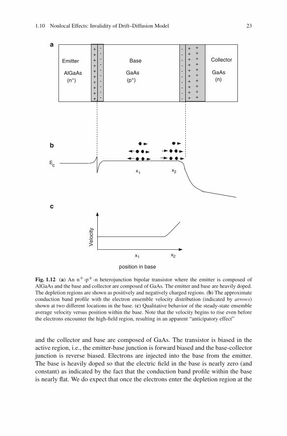
1.10 Nonlocal Effects: Invalidity of Drift–Diffusion Model 23
++++++++++
----------
----------
++++++++++
++++++++++
AlGaAs GaAs GaAs
(n+) (p+) (n)
Emitter Base Collector
Ecx x21
x1 x2
position in base
Vel
ocity
a
b
c
Fig. 1.12 (a) An nC-pC-n heterojunction bipolar transistor where the emitter is composed ofAlGaAs and the base and collector are composed of GaAs. The emitter and base are heavily doped.The depletion regions are shown as positively and negatively charged regions. (b) The approximateconduction band profile with the electron ensemble velocity distribution (indicated by arrows)shown at two different locations in the base. (c) Qualitative behavior of the steady-state ensembleaverage velocity versus position within the base. Note that the velocity begins to rise even beforethe electrons encounter the high-field region, resulting in an apparent “anticipatory effect”
and the collector and base are composed of GaAs. The transistor is biased in theactive region, i.e., the emitter-base junction is forward biased and the base-collectorjunction is reverse biased. Electrons are injected into the base from the emitter.The base is heavily doped so that the electric field in the base is nearly zero (andconstant) as indicated by the fact that the conduction band profile within the baseis nearly flat. We do expect that once the electrons enter the depletion region at the

24 1 Charge and Current in Solids: The Classical Drift–Diffusion Model
base-collector junction,9 they will encounter a high electric field and the steady-statedrift velocity should begin to rise. But in reality, the steady-state drift velocity beginsto rise well before the electrons enter the depletion region at the base-collectorinterface and encounter the high electric field region [4]. This is shown in Fig. 1.12c.It is as if the electrons are prescient and can anticipate the high-field region, so thattheir average velocity begins to rise even before encountering the high electric field!This means that the drift velocity (and hence the electron mobility) is no longera function of the local electric field, since if it were, then it would be the samethroughout the electrically neutral base since the electric field is the same throughoutthe neutral base.
What really happens here is the following. The steady-state drift velocity at anylocation is determined by the ensemble average of the steady-state velocities of allthe electrons at that location. Far to the left of the base-collector junction, say atlocation x1, the ensemble has both right- and left-moving electrons. Electrons thathave scattered forward from regions to the left of x1 are traveling to the right atx1, and electrons that have scattered backward from regions to the right of x1 aretraveling to the left at x1. Because of the presence of electrons with both positiveand negative velocity components at x1, the ensemble average velocity here issmall since the positive and negative components tend to offset each other. Now,just to the left of the base-collector junction, say at location x2, the left-travelingelectrons are virtually absent since electrons from the collector region will nevertravel back into the base because of the huge accelerating electric field in the base-collector depletion region that inexorably sweeps them forward, away from the base.Viewed differently, there is a huge potential barrier at the base-collector junction thatprevents electrons from the collector traveling back into the base and increasing thefraction of left traveling electrons at x2. Consequently, the ensemble average steady-state velocity at x2 is much higher than what it is at x1, even though the local electricfields at x1 and x2 are about the same. Therefore, the velocity (and mobility) are notfunctions of the local electric field alone. This is a dramatic illustration of nonlocaleffects. The drift velocity begins to rise when electrons reach the location x2, eventhough the electric field at x2 is still very weak. This is the basis of the “anticipatoryeffect.”
Needless to say, such an effect cannot be captured within the standard drift–diffusion model. The drift–diffusion model fails here since assumption 2 is violated.There is not enough backscattering near the collector edge within the base toallow the electron ensemble to reach local equilibrium with the surroundings.The inevitable aftermath is nonlocal effects that invalidate the drift–diffusion model.
The final issue to address before we conclude this chapter is how does one goabout determining the transport parameters mobility and diffusion coefficient forboth electrons and holes at different locations within a piece of solid. These quan-tities appear in the drift–diffusion equations, i.e., (1.31), and must be known before
9Because of the much heavier doping in the base compared to the collector, the depletion regionresides mostly in the collector and hence starts almost at the base-collector metallurgical junction.

1.10 Nonlocal Effects: Invalidity of Drift–Diffusion Model 25
we can solve (1.31) to find the steady-state transport variables Jn.Er/; Jp.Er/, n.Er/,and p.Er/. As long as there are no nonlocal effects, we can always find the mobilityfrom the velocity field relationships of the type shown in Fig. 1.9. The diffusioncoefficient can then be related to the mobility by the so-called Einstein relationdiscussed next. This relation is at least approximately valid as long as the currentdensity is small, quasi equilibrium conditions prevail, and the semiconductor isnondegenerate. Therefore, we can determine the transport parameters if no nonlocaleffect shows up. However, all bets are off if nonlocal effects take hold. In that case,the transport parameters cannot be expressed as functions of the local electric field,or any other variable that depends only on the local coordinate, and the entire drift–diffusion model fails. In fact, the mobility and diffusion coefficient then becomefunctionals of a certain function known as the distribution function f .Er; Ek; t/, whichis the probability of finding an electron at a position Er , with a wavevector Ek, at aninstant of time t . The distribution function can be found by solving the BoltzmannTransport equation (BTE) which is the subject of the next chapter.
Special Topic 2: The Einstein relation
The Einstein relation relates the diffusion coefficient to the drift mobility in anondegenerate semiconductor under global equilibrium conditions. When globalequilibrium exists, no electron or hole current is flowing through the semiconductor.However, if some electron or hole current is flowing but it is small, then we can saythat quasi-equilibrium condition prevails. In that case, the Einstein relation will beapproximately valid. We will derive this relation here.
A nondegenerate semiconductor is one where the Fermi level is at least 3kBT
energy below the conduction band edge and 3kBT energy above the valence bandedge (kB is the Boltzmann constant and T is the absolute ambient temperature). Insuch a semiconductor, the steady-state electron concentration is related to the Fermilevel �F
10 as
n.Er/ D Nce�F�Ec0.Er/
kBT ; (1.34)
where Nc is the effective density of states in the conduction band and Ec0 is theconduction band edge. We will derive this relation later in Chap. 4. The quantity Nc
depends on the effective mass of the electron and temperature, which we assume to
10The Fermi level �F is defined in the following way: the probability that an electron in asolid under global equilibrium has total energy (kinetic C potential) equal to the Fermi level�F is exactly one-half or 50%. This follows from Fermi–Dirac statistics which dictates that theprobability of finding an electron with total energy E under global equilibrium is 1=fexpŒ.E ��F/� C 1g.

26 1 Charge and Current in Solids: The Classical Drift–Diffusion Model
be spatially invariant. We will also show in Chap. 2 that if the effective mass andtemperature are spatially invariant, then the Fermi level �F does not vary in spaceas long as the semiconductor is in global equilibrium.
Using this result in the electron current equation in (1.31), and setting Jn D 0 forglobal equilibrium, we get
0 D Nce�F�Ec0.Er/
kBT e�n.Er/ EE.Er/ C eDn.Er/ Err
�
Nce�F�Ec0.Er/
kBT
�
; (1.35)
which simplifies to
0 D �n.Er/ EE.Er/ � Dn.Er/1
kBTErrEc0.Er/: (1.36)
Now, the electric field is the negative of the potential gradient, so that ErrEc0.Er/ De EE.Er/. Therefore, we immediately get
Dn.Er/ D kBT
e�n.Er/: (1.37)
Similarly, it can be shown that
Dp.Er/ D kBT
e�p.Er/: (1.38)
The above relations between the local diffusion coefficient and mobility arecollectively known as the Einstein relation.
Special Topic 3: Shockley–Read–Hall recombination
Whenever the concentrations of electrons and holes in a semiconductor exceed thelocal equilibrium concentrations n0.Er; t/ and p0.Er; t/, the excess electrons and holesrecombine radiatively and/or nonradiatively to restore local equilibrium conditions.Similarly, whenever the concentrations are less than the local equilibrium concentra-tions, electrons and holes are generated (nonradiatively, if there are no light sourcespresent) until local equilibrium is restored.
Shockley, Read, and Hall developed an expression for the recombination rate ofelectrons and holes, which stated
Rn.Er; t/ D Rp.Er; t/
D n.Er; t/p.Er; t/ � n0.Er; t/p0.Er; t/
�p0.Er; t/Œn.Er; t/ C ni .Er; t/� C �n0.Er; t/Œ.p.Er; t/ C ni .Er; t/�; (1.39)

1.11 Summary 27
where ni is the intrinsic carrier concentration in the semiconductor, n and p arethe electron and hole concentrations, and �p0, �n0 are lifetimes associated withrecombination and generation processes.
We can write
n.Er/ D n0.Er/ C n.Er/
p.Er/ D p0.Er/ C p.Er/; (1.40)
which reduces the last equation to
Rn.Er; t / D Rp.Er; t /
D n.Er; t /p.Er; t / C n.Er; t /.n0.Er; t / C p0.Er; t //
�p.Er; t /.n0.Er ; t / C ni .Er ; t / C n.Er; t // C �n.Er; t /.p0.Er; t / C ni .Er; t / C n.Er; t //;
(1.41)
where we have used the fact that because electrons and holes always generateor recombine in pairs (charge neutrality), n.Er; t/ D p.Er; t/. Furthermore, thedeviations from local equilibrium are assumed to be small so that we can neglectproduct terms np. Finally, defining a quantity
�R.Er; t/ D �p.Er; t/.n0.Er; t/ C ni .Er; t// C �n.Er; t/.p0.Er; t/ C ni .Er; t//
n0.Er; t/ C p0.Er; t/(1.42)
and recognizing that as long as we are not too far off equilibrium (known as lowlevel injection conditions), n.Er/ D p.Er; t/ � ni .Er; t/, we get
Rn.Er; t/ D Rp.Er; t/ D n.Er; t/
�R.Er; t/D p.Er; t/
�R.Er; t/: (1.43)
The above equation is the expression for the Shockley–Reed–Hall recombinationrate.
1.11 Summary
In this chapter, we learned about the drift–diffusion model. The important points toremember are:
1. The drift–diffusion model is predicated on two basic assumptions about thenature of charge transport in a solid, namely that (1) charge carriers areclassical particles obeying Newton’s laws, and (2) they experience forces dueto external electric and/or magnetic fields as well as scattering. The latter tends

28 1 Charge and Current in Solids: The Classical Drift–Diffusion Model
to restore local equilibrium. A carrier scatters many times before the electricand/or magnetic fields change significantly, so that a carrier is always at localequilibrium with its surroundings.
2. The single particle drift model is the Drude model of conduction that yieldsOhm’s law.
3. Electron and hole drift current densities at any location within a solid alwayspoint in the same direction, which is the direction of the local electric field.
4. Electron diffusion current density at any location points in the direction of thelocal electron concentration gradient, while the hole diffusion current densitypoints opposite to the direction of the local hole concentration gradient.
5. Steady-state transport variables, like current densities EJp.Er/, EJn.Er/ and carrierconcentrations p.Er/, n.Er/, at any location in space, are found by simultaneouslysolving the continuity equations, current equations, and Poisson equation (1.31).These equations are collectively known as the “equations of state.” In order tosolve them, we must know the transport parameters mobility [�p.Er/, �n.Er/] anddiffusion coefficient [Dp.Er/, Dn.Er/] everywhere in the device. In the absence ofnonlocal effects (which would have invalidated the drift–diffusion model in anycase), the mobility can be found from the known drift velocity versus electricfield characteristics in the material, and the diffusion coefficient can be related tothe mobility by the Einstein relation.
6. The drift–diffusion model can handle local nonlinear effects, such as velocitysaturation or negative differential mobility, by defining transport parameters—mobilities and diffusion coefficients—as functions of the local electric field.
7. The drift–diffusion model breaks down in the presence of nonlocal effects thatarise when carriers fail to reach local equilibrium with their surroundings. Thiscan happen in devices with rapid compositional or doping variations (recallthe device in Fig. 1.12) which make the electric field in the device change sorapidly in space that a charge carrier does not have the opportunity to scattermany times before the field changes significantly. This prevents the charge carrierfrom equilibrating with the local environment, so that its behavior is no longerdetermined uniquely by its local surroundings. Nonlocal effects can also arise inultrasmall devices where transport is quasi-ballistic and velocity overshoot canoccur.
Problems
Problem 1.1. Newton’s second law states
d Ep.Er; t/
dtD EF .Er; t/: (1.44)

Problems 29
where Ep is a particle’s momentum and the force EF is usually defined as
EF .Er; t/ D � ErrU.Er; t/; (1.45)
where Err is the spatial gradient and U.Er; t/ is the potential energy .Hamiltonian mechanics treats Ep and Er as independent variables and postulates
dErdt
D ErpH.Er.t/; Ep.t//ˇˇˇErDconstant
d Epdt
D � ErrH.Er.t/; Ep.t//ˇˇˇ EpDconstant
; (1.46)
where Erp is the momentum gradient and H is the Hamiltonian which is the sum ofkinetic energy T and potential energy U .
Consider the situation when the mass of the particle varies in space. If we definemomentum as Ep.Er; t/ D m.Er; t/Ev.Er; t/ and T .Er; t/ D p2.Er; t/=2m.Er; t/, show thatthe first of Hamilton’s equation in (1.46) is satisfied. Show also that the second ofHamilton’s equations, (1.44) and (1.45) cannot all be satisfied. Which of these threeequations need to be modified in the case of spatially varying mass so that all threeequations can be satisfied simultaneously? Note that if mass did not vary in space,then ErrT j EpDconstant D 0, but otherwise it is nonzero.
Problem 1.2. In this chapter, we saw that current is carried in a solid by electronsand holes that drift and diffuse. Such current is called “conduction current” sinceit is caused by the flow (or conduction) of actual charged particles. There can beanother type of current in a solid (or even vacuum), called “displacement current,”which does not require flow of particles. It is caused by the time variation of thedisplacement vector which is the product of the dielectric constant � and the electricfield EE in a medium. Both types of current can give rise to a magnetic field accordingto the well-known Ampere’s law.
Maxwell’s equation provides a mathematical statement of Ampere’s law. Themagnetic field intensity H arising from conduction and displacement currents arerelated to those currents by the relation
Err � EH D EJ C @.� EE/
@t;
where the first term in the right-hand side is the conduction current, and the secondterm is the displacement current.
Using the above equation and Poisson equation, derive the nonsteady-statecontinuity equation
Err � EJ C @�
@tD 0;

30 1 Charge and Current in Solids: The Classical Drift–Diffusion Model
in the absence of any recombination or generation. Here, � is the charge density.We will derive this equation in the next chapter from the BTE. This equationimmediately shows that in the absence of any recombination and generation, thesteady-state conduction current density must be spatially invariant.
Problem 1.3. Consider a situation when minority carrier electrons are injectedinto a piece of p-type semiconductor where the electric field is weak. Assumingthat the equilibrium minority carrier concentration n0 does not vary with positionor time, show that the excess minority carrier concentration n.Er; t/ obeys theequation
@n.Er; t/
@t� Dnr2
r n.Er; t/ C Gn.Er; t/ � n.Er; t/
�R.Er; t/
if we assume that the diffusion coefficient is spatially invariant and therecombination rate is given by the Shockley–Read–Hall expression.
Hint: Use the equation in Problem 1.1 and add the generation and recombinationterms on the right-hand-side of that equation. Then express the conduction currentin terms of its drift and diffusion components.
The above equation is called the minority carrier diffusion equation. Can thisequation be applied to find the minority carrier concentration at the edge of thedepletion region of a diode?
Problem 1.4. Consider a one-dimensional n-type semiconductor structure oflength L stretching from coordinate x D 0 to x D L. There is no recombination orgeneration inside this structure since the semiconductor is maintained in the darkand the nonradiative lifetime is extremely long. Minority carrier holes are injectedfrom the end x D 0 and the electric field inside the semiconductor is uniform andequal to E . Assume that the current through the semiconductor is small enoughthat Einstein relation is approximately valid. Assume also that the hole mobilityis spatially invariant. Show that the steady-state minority hole concentration isgiven by
p.x/ D p.L/
2 exp.eEL=2kBT / sinh.eEL=2kBT /
�
exp
�eE
kBTx
�
� 1
�
:
if the hole concentration at x D 0 is zero.
Problem 1.5. Under steady-state conditions, is the ensemble average velocityalways the same as the drift velocity?
Solution. No. The drift velocity is the velocity imparted by the electric field.However, carriers can have a net velocity due to diffusion when carriers migratefrom a region of high concentration to a region of low concentration. This “diffusionvelocity” contributes to the ensemble average velocity but has nothing to do withany electric field. Hence, the ensemble average velocity need not be equal to thedrift velocity.

Problems 31
Problem 1.6. Consider a bar of nondegenerate semiconductor doped with spatiallyvarying donor concentration ND.x/ = ND.0/e�x=L. Assume that ND.x/ � ni ,where ni is the intrinsic carrier concentration in the semiconductor. Assume that allthe donors are ionized. Show that under equilibrium, there will be a homogeneousbuilt-in electric field within the semiconductor. Find the strength of this electricfield at room temperature if L D 1�m. Does this electric field satisfy the Poissonequation?
Solution. Since all the donors are ionized,
n.x/ D ND.x/ D ND.0/ expŒ�x=L�:
The law of mass action (students should be familiar with this law; otherwise, see[6]) mandates that at equilibrium,
n.x/p.x/ D n2i :
Hence, p.x/ D n2i =n.x/ � ni � 0 since n.x/ D ND.x/ � ni .
At equilibrium, Jn.x/ D 0. Therefore, we can write
0 D e�n.x/n.x/E.x/ C eDn.x/dn.x/
dx;
where E.x/ is the electric field in the semiconductor.Using Einstein relation, we can write
0 D e�n.x/ND.0/ expŒ�x=L�E.x/ C ekBT
e�n.x/
�
� 1
L
�
ND.0/ expŒ�x=L�;
which yields
E.x/ D kBT
eL:
Note that the electric field turns out to be spatially invariant (independent of x);hence, it is homogeneous.
At room temperature, kBT=e D 26 mV. Therefore, the strength of this field is 26kV/m everywhere since L D 1 �m.
The Poisson equation states
�dE.x/
dxD eŒND.x/ C p.x/ � n.x/� D e
�
ND.x/ C n2i
n.x/� n.x/
�
� 0:
Since the electric field is homogeneous, its spatial derivative vanishes andPoisson’s equation is satisfied.
Problem 1.7. Consider an infinite one-dimensional silicon bar whose central sec-tion extending from x D �L to x D L is selectively illuminated with light that

32 1 Charge and Current in Solids: The Classical Drift–Diffusion Model
Light
0 L–L
Fig. 1.13 A uniformly doped infinite semiconductor bar whose central region extending fromx D �L to x D L is illuminated. There is no electric field inside the semiconductor
generates G electron-hole pairs per unit volume per unit time. The semiconductor isuniformly doped with Boron at a level of 1018 cm�3. There is no electric field insidethe semiconductor since it is uniformly doped and no battery is connected acrossit. Refer to Fig. 1.13 for this problem. (Hint: You should use the minority carrierdiffusion equation derived in Problem 1.2 for this exercise.)
1. If the semiconductor were not uniformly doped, would an electric field inevitablyexist inside the semiconductor at equilibrium? Explain.
2. Explain why the excess minority carrier concentration generated by light and itsfirst derivative must be continuous everywhere.
3. If the semiconductor is maintained at steady-state, derive an equation for theminority carrier concentration everywhere.
Problem 1.8. Consider a nonuniformly doped semiconductor doped with donors.The majority carrier concentration is approximately equal to the donor concentrationeverywhere.
Apply Poisson equation to derive an expression for the intrinsic level profile[Ei.x/ versus x] at equilibrium assuming that the semiconductor is nondegenerate,which allows one to use the equation
p.x/ D ni exp
�Ei.x/ � �F
kBT
�
;
where ni is the intrinsic carrier concentration and �F is the Fermi level.
References 33
The intrinsic level is approximately half-way between the conduction andvalence band edges and is given by Ei � Ec0CEv0
2. The electric field inside the
semiconductor is related to the intrinsic level as E.x/ D 1e
dEi .x/
dx.
Show that if the intrinsic level intersects the Fermi level at x D 0 and at thatpoint the electric field is zero, then the intrinsic level profile in the vicinity of thatregion can be written as
Ei .x/ D �F C kBT
�
1 � cosh
�x
LD
��
;
where LD Dq
�r�0kBTe2ni
is called the intrinsic Debye length.
Problem 1.9. Consider an n-type semiconductor bar that is at steady state but notat equilibrium since a small current is flowing through it. If the majority carrierconcentration varies linearly in space, then show that the built-in electric field E.x/
in the semiconductor obeys the equation (in one dimension):
dn.x/
dxE.x/ C n.x/
dE.x/
dxD 0:
References
1. B. K. Ridley and T. B. Watkins, “The possibility of negative resistance effect in semiconduc-tors”, Proc. Phys. Soc. Lond., 78, 293 (1961).
2. C. Hilsum, “Transferred electron amplifiers and oscillators”, Proc. IRE, 50, 185 (1962).3. J. B. Gunn, “Microwave oscillation of current in III-V semiconductors”, Solid State Commun.,
1, 88 (1963).4. S. Bandyopadhyay, M. E. Klausmeier-Brown, C. M. Maziar, S. Datta and M. S. Lundstrom,
“A rigorous technique to couple Monte Carlo and drift–diffusion models for computationallyefficient device simulation”, IEEE Trans. Elec. Dev., 34, 392 (1987).
5. S. M. Sze, Physics of Semiconductor Devices, 2nd. edition, (John Wiley & Sons, New York,1981).
6. R. F. Pierret, Semiconductor Device Fundamentals (Addison Wesley Longman, Reading,Massachusetts, 1996).

Chapter 2Boltzmann Transport: Beyondthe Drift–Diffusion Model
2.1 Transport in the Presence of Nonlocal Effects:The Carrier Distribution Function
In the previous chapter, we mentioned that when nonlocal effects are present,transport parameters—such as mobility and diffusion coefficient—become func-tionals of a quantity known as the carrier distribution function. This quantityf .Er; Ek; t/ is the probability of finding an electron at a position Er , with a wavevectorEk at an instant of time t .1
The distribution function f .Er; Ek; t/ is a function in 7-dimensional phase space(three coordinates of Er , three coordinates of Ek, and one coordinate of t). Beinga “probability,” it is always positive indefinite (i.e., its value is never negative).In order to determine this quantity (which we must determine if we wish to findtransport parameters in the presence of nonlocal effects), we have to solve anequation known as the BTE which we discuss in this chapter. Once the distributionfunction is found from the BTE, we can find any transport parameter as a function ofposition Er and time t from the distribution function.
At a given location Er in a solid and at a given instant of time t , the distributionfunction f .Er; Ek; t/ will tell us the probability of finding an electron with awavevector Ek, or velocity Ev which is a single-valued function of Ek. If there are Nelectrons in that location at that instant of time, it will tell us how many of them havewavevectors between Ek1�� Ek1 and Ek1C� Ek1, how many have wavevectors between
1The electron’s wavevector may seem to be a quantum-mechanical attribute since only a wave hasa wavevector and the electron behaves as a wave only in the domain of quantum mechanics. TheBoltzmann transport formalism is however almost entirely classical. The wavevector is uniquelyrelated to the electron’s velocity which may appear to be more of a classical attribute. We could
have defined the distribution function as f .Er;Ev; t /, but is more common to define it as f .Er ; Ek; t/since it is easy to count electron states in wavevector space. This will become clearer when wediscuss the concept of density of states in a later chapter.
S. Bandyopadhyay, Physics of Nanostructured Solid State Devices,DOI 10.1007/978-1-4614-1141-3 2, © Springer Science+Business Media, LLC 2012
35

36 2 Boltzmann Transport: Beyond the Drift–Diffusion Model
Ek2 �� Ek2 and Ek2 C� Ek2, etc. In the example of Fig. 1.12, it would have told us thatthere are very few electrons with negative wavevectors at x2 (or that the probabilityof finding an electron with negative wavevector is very small there). Therefore, itwould have correctly predicted the anticipatory rise in the ensemble average velocityat x D x2. In other words, it would have correctly described nonlocal effects.
Now, we said that the transport parameters are functionals of the distributionfunction and therefore we can determine them if we know the distribution function.The procedure for doing this is straightforward but unfortunately, it is cumbersome,as we shall see later. However, the utility of transport parameters is ultimately infinding transport variables from (1.31). What if it were possible to find the transportvariables directly from the distribution function, without having to first evaluate thetransport parameters and then finding the transport variables from (1.31)? This isnot only possible, but preferred since it is direct. The transport variables can befound directly from the distribution function since they are nothing but different“moments” of the distribution function. For example,
n.Er; t/ D 1
˝
X
Ekf .Er; Ek; t/ D 1
4�3
Z
d3 Ek f .Er; Ek; t/ .0-th moment/
EJn.Er; t/ D �e˝
X
EkEv.Ek/f .Er; Ek; t/ D �e
4�3
Z
d3 Ek Ev.Ek/f .Er; Ek; t/ .1st: moment/
�n.Er; t/ D 1
˝
X
EkE.Ek/f .Er; Ek; t/ D 1
4�3
Z
d3 EkE.Ek/f .Er; Ek; t/ .2nd: moment/
(2.1)
and so on. Here, �n.Er; t/ is the electron energy density at location Er at time t , E.Ek/is the energy of an electron with wavevector Ek, Ev.Ek/ is the velocity of an electronwith wavevector Ek, and ˝ is a normalizing volume, which does not matter in theend since the right-hand sides are independent of this quantity.
This direct approach appears to be far better than finding the transport parametersfrom the distribution function and then solving (1.31) to find the transport variables.However, there is one caveat. Since the distribution function is a 7-dimensionalfunction, the BTE is not easy to solve. It is usually solved numerically orwith MC simulation. Both techniques are computationally demanding and requireconsiderable resources. Therefore, it is sometimes more efficient to solve the BTEonly in selected regions of a device where we suspect that nonlocal effects willprevail, instead of solving it globally. From these solutions, we can extract thetransport parameters in the suspect regions, while the transport parameters in theremaining regions are found from local field-dependent models (such as from thevelocity-field characteristic of Fig. 1.9). Finally, we can solve the drift–diffusionequation (1.31) globally using the transport parameters found in every region ofthe device. This kind of an approach, although seemingly indirect and tortuous,

2.2 Boltzmann Transport Equation for the Carrier Distribution Function 37
is actually computationally more efficient in many cases and is used in commercialdevice simulation packages such as MINIMOS that analyze charge transport in solidstate devices.
2.2 Boltzmann Transport Equation for the CarrierDistribution Function
We are now ready to introduce the BTE. It is really nothing but a statement about theconservation of particles (or charge). Since it is difficult for us humans to mentallyvisualize a 7-dimensional phase space, let us consider a simpler situation wherethere is only one spatial dimension x, one wavevector dimension kx , and time t . Forthe purpose of this discussion, we have mentally shrunk the 7-dimensional phasespace to a 3-dimensional phase space because it is easy to visualize.
Now consider a rectangular “box” located at .x; kx; t/ which has dimensions�x, �kx , and �t , as shown in Fig. 2.1. The number of electrons within this box isproportional to the probability of finding an electron at position x, with wavevectorkx at time t , or, in other words, it is proportional to f .x; kx; t/. The rate at whichthe number of electrons within this box is changing must be equal to the differenceof the rate at which electrons are scattering into this box from the outside and therate at which electrons are scattering out of this box to the outside. Electrons cannotspontaneously appear or disappear within this box because of the conservation ofparticles or conservation of charge. Therefore, we can write:
df .x; kx; t/
dtD df .x; kx; t/
dt
ˇˇˇˇscatter-in
� df .x; kx; t/
dt
ˇˇˇˇscatter-out
D Sin � Sout: (2.2)
Δx
Δt
Δkx
Scattering out Scattering in
Fig. 2.1 A rectangular box inthree-dimensional phasespace located at .x; kx; t /.The box has dimensions of�x,�kx , and �t . Thenumber of electrons in thisbox is proportional tof .x; kx; t /. Because ofcharge conservation, the onlyway the number of electronswithin this box can change isif electrons scatter into thisbox from outside to increasethe number, or scatter fromthis box to the outside todecrease the number

38 2 Boltzmann Transport: Beyond the Drift–Diffusion Model
Generalizing back to seven dimensions and converting the total derivative in theleft-hand side to partial derivatives, we get
df .Er; Ek; t/dt
D @f .Er; Ek; t/@t
C @f .Er ; Ek; t/@Er � dEr
dtC @f .Er; Ek; t/
@Ek� d Ekdt
D Sin�Sout; (2.3)
where Sin and Sout are the in- and out-scattering rates.Now, Newton’s second law tells us that the force on a particle in a crystal is equal
to the rate of change of crystal momentum „Ek:
EF .Er; t/ D d.„Ek/dt
: (2.4)
Furthermore, by definition,
dErdt
D Ev.Ek/; (2.5)
where Ev is the velocity. Using these two results in (2.3), we get:
@f .Er; Ek; t/@t
C Ev.Ek/ � Errf .Er; Ek; t/CEF .Er; t/
„ � Erkf .Er; Ek; t/ D Sin � Sout; (2.6)
where Err represents gradient in real space and Erk represents gradient in wavevectorspace.
We are almost there, but we have one last step to complete. We need to findmore explicit expressions for Sin and Sout. The former is the rate of scattering intothe “box” from outside the “box,” i.e., from all other wavevector states Ek0, fromall other sites Er 0, and from all other times t 0. However, in the Boltzmann picture,scattering events are always considered to be instantaneous in both time and space,i.e., Er D Er 0 and t D t 0. Therefore, the in-scattering rate is the rate of scattering fromall wavevector states Ek0 to the wavevector state Ek, multiplied by the probability thatthe wavevector state Ek0 is occupied to begin with so that an electron can scatter infrom that state, multiplied by the probability that the wavevector state Ek is empty toscatter into. The last requirement comes about from the Pauli Exclusion Principlethat prohibits two electrons from occupying the same wavevector state Ek. In realityup to two electrons can occupy the wavevector state Ek, but they must have oppositespins. The BTE, however, does not account for spin.2 Hence,
2If we wished to account for spin in the BTE, we could have written one BTE for each spin and thenintroduced a coupling term to couple the two BTE-s. The coupling term would have been a termto represent spin-flip scattering. This is an approach implicit in the drift–diffusion model of spintransport but it has some limitations. An arbitrary spin can be written as the coherent superpositionof two antiparallel spins. Spin precession about a magnetic field is equivalent to continuously

2.2 Boltzmann Transport Equation for the Carrier Distribution Function 39
Sin DX
Ek0
S� Ek0; Ek
�
f�
Er; Ek0; t� h
1 � f�
Er; Ek; t�i
Sout DX
Ek0
S� Ek; Ek0�f
�
Er; Ek; t� h
1 � f�
Er; Ek0; t�i
; (2.7)
where S.Ek1; Ek2/ is the rate at which a particle scatters from a wavevector state Ek1 toa wavevector state Ek2.
Therefore, the final form of the BTE is
@f�
Er; Ek; t�
@tC Ev
� Ek�
� Errf�
Er; Ek; t�
CEF �Er; t�
„ � Erkf�
Er; Ek; t�
DX
Ek0
S�Ek0; Ek
�
f�
Er; Ek0; t� h
1 � f�
Er; Ek; t�i
�X
Ek0
S� Ek; Ek0
�
f�
Er; Ek; t� h
1 � f�
Er; Ek0; t�i
: (2.8)
Note that the left-hand-side contains derivatives in wavevector space whereasthe right-hand-side contains summations (or equivalently integrals) in wavevectorspace. Hence, the BTE is an integro-differential equation.
2.2.1 Limitations of the BTE
At the outset, let us point out that the BTE is purely classical and does not accountfor any quantum-mechanical effect. It cannot. Note that the distribution functionf .Er; Ek; t/ is a function of both Er and Ek. This is forbidden by the laws of quantummechanics since Er and Ek are Fourier transform pairs and obey the HeisenbergUncertainty relation
�Er �� Ek � „2: (2.9)
That means both a position Er and a wavevector Ek cannot be defined at the sametime with precision, according to quantum mechanics. In other words, a functionsuch as f .Er; Ek; t/, which is simultaneously a function of both Er and Ek, cannot
changing the phase relationship between the two components coherently. This coherence aspectcannot be included satisfactorily in such an approach, which is why the coupled BTE method isnot an accurate way to model spin transport.

40 2 Boltzmann Transport: Beyond the Drift–Diffusion Model
even exist according to orthodox quantum mechanics. Therefore, the BTE cannever model quantum-mechanical effects. Furthermore, quantum mechanics allowsinterference between electron waves. Destructive interference would involve twowaves canceling each other out to produce a “null’ or “zero.” BTE can never modelsuch an effect since the distribution function is never negative. To produce a zero, anegative quantity must cancel a positive quantity. That is not possible if the quantityin question can never be negative.
Quantum mechanical effects arise when charge carriers cease to behave asclassical particles like billiard balls, and instead behave as waves propagatingthrough a device in accordance with the Schrodinger equation. Starting in themid-1980s, a branch of physics, known as “mesoscopic physics,” emerged thatdeals with such situations in ultrasmall metal and semiconductor structures [1–4].These structures are so small that an electron can traverse them without suffering asingle phonon collision or collision with another electron. Such inelastic collisionswould have randomized the electron’s phase and restored its particle nature, butif they are infrequent or absent, the wave nature is preserved. Charge transport insuch structures cannot be captured by the BTE, but will require strictly quantum-mechanical formulations. Many such formulations exist and some are discussed inChap. 8.
2.2.2 Limits of Validity of the BTE
The Heisenberg Uncertainty Principle sets limits on the validity of the BTE. ThisPrinciple states
�E�t � „2; (2.10)
where �E is the uncertainty in the carrier’s energy and �t is the associateduncertainty in time. Therefore, the carrier must remain in a state for a sufficientlylong time to have a well-defined energyE (or wavevector k, since the latter is relatedto the energy). If we assume that the electron remains in a fixed energy state betweentwo successive inelastic collisions (which always change the electron’s energy), thenwe can set �t D �inelastic, which is the mean time between inelastic collisions. Now,if we assume that the electron energy level is thermally broadened to the effect that�E D kBT [5], then we require that
�inelastic � „2kBT
: (2.11)
At room temperature, this means that the inelastic scattering time should farexceed 12.5 fs for the BTE to be valid („=.2kBT / D 12.5 fs at room temperature).In some metals with high electron concentration, the electron–electron scattering(an inelastic scattering process) can be frequent enough that the above inequality isnot fulfilled. In that case, the BTE is not valid.

2.3 The Generalized Moment Equation or Hydrodynamic Balance Equation 41
Note that if the inelastic scattering time is too long, the BTE may be invalidatedbecause the wave nature of electrons will be manifested. On the other hand, if itis too short, then the BTE may be invalidated again because of the UncertaintyPrinciple. Thus, there is a range of the inelastic scattering time over which the BTEis meaningful.
2.3 The Generalized Moment Equation or HydrodynamicBalance Equation
In the last chapter, we stated that there is a transient (or time-varying) version of theequations of state, even though we derived (1.31) only for steady-state situations.In this section, we will show how to generalize (1.31) to the transient case. In fact,we will derive a general equation from the BTE which will yield the continuityequation and the current equation of (1.31) as mere special cases. This generalequation will allow us to derive not just (1.31), but an equation for any arbitrarytransport variable, that is valid for both steady-state and nonsteady-state situations.In order to accomplish this, we will first define a general moment of the distributionfunction and show that this moment obeys an equation that is variously known asthe “generalized moment equation,” or “hydrodynamic balance equation” becauseof its similarity with the equations of hydrodynamics. Once we obtain this equation,we will show how the current and continuity equations of the preceding chaptercan be derived as corollaries. Moreover, this new equation will allow us to extendthe equations of state to nonsteady-state or time-varying situations. Clearly, sincethe drift–diffusion equations can be derived from the BTE, but not the other wayaround, it is obvious that the Boltzmann model is more advanced and powerful thanthe drift–diffusion model.
Let us define the m-th moment of the distribution function as the quantity
Gm.Er; t/ DX
Ekg.km/f .Er; Ek; t/; (2.12)
where g.km/ is a scalar, vector, or tensor function of km, the m-th power of thewavevector.
Multiplying both sides of the BTE in (2.8) with g.km/ and summing over all Ek,we get
X
Ekg.km/
@f .Er ; Ek; t/@t
CX
Ekg.km/Ev.Ek/ � Errf .Er; Ek; t/
CX
Ekg.km/
EF .Er; t/„ � Erkf .Er; Ek; t/

42 2 Boltzmann Transport: Beyond the Drift–Diffusion Model
DX
Ekg.km/
8
<
:
X
Ek0
S.Ek0; Ek/f .Er; Ek0; t/Œ1 � f .Er; Ek; t/�
�X
Ek0
S.Ek; Ek0/f .Er; Ek; t/Œ1 � f .Er; Ek0; t/�
9
=
;: (2.13)
Since g.km/ is a function of only wavevector and not time, the first term on theleft-hand-side of (2.13) can be simplified to
X
Ekg.km/
@f .Er; Ek; t/@t
DX
Ek
@Œg.km/f .Er; Ek; t/�@t
D@nP
EkŒg.km/f .Er; Ek; t/�
o
@t
D @Gm.Er; t/@t
(2.14)
To evaluate the second term on the left-hand-side of (2.13), we need to use thevector identity
Er � . EV S/ D S Er � EV C EV � ErS; (2.15)
where EV is a vector and S is a scalar.The second term becomes
X
Ekg.km/Ev.Ek/ � Errf .Er; Ek; t/ D
X
Ekg.km/
n Err �h
Ev.Ek/f .Er; Ek; t/i
�f .Er; Ek; t/ Err � Ev.Ek/o
D8
<
:
Err �X
Ekg.km/Ev.Ek/f .Er; Ek; t/
9
=
;
D Err � EJGm.Er; t/; (2.16)
where we have used the fact that since Er , Ek, and t are independent variables, neitherEv.Ek/ nor g.km/ will be functions of Er unless the quantities that relate Ev.Ek/ or g.km/with k change in space or time. The latter can happen, for example, if the materialhas a spatially varying bandstructure that makes the effective mass spatially variant.In that case, Ev.Ek/ will depend on vecr, but we will not be considering such situationshere. The quantity EJGm.Er; t/ is called “flux of the momentGm.Er; t/”. Note that since

2.3 The Generalized Moment Equation or Hydrodynamic Balance Equation 43
Ev.Ek/ is roughly proportional to k (in metals or semiconductors with approximatelyparabolic band structures), this flux is like the .mC1/-th moment of the distributionfunction.
Using the vector identity in (2.15), we can write the third term on the left-handside of (2.13) as
X
Ek
g.km/EF .Er; t/
„ � Erkf .Er; Ek; t/ DX
Ek
(
Erk�"
g.km/EF .Er; t/
„ f .Er; Ek; t/#
�f .Er; Ek; t/ Erk �"
g.km/EF .Er; t/
„
#)
: (2.17)
The first term on the right-hand-side in the last equation can be written as
X
EkErk �
"
g.km/EF .Er; t/
„ f .Er; Ek; t/#
/Z 1
�1
@
�
g.km/EF .Er;t /
„ f .Er; Ek; t/�
@EkdEk
DEF .Er; t/
„˚
g.1/f .Er;1; t/� g.�1/f .Er;�1; t/�
D 0; (2.18)
This term vanishes since the distribution function is bounded and must vanish whenEk D ˙1.3
Using (2.15) yet again, the second term on the right-hand-side of (2.17) can bewritten as
X
Ekf .Er; Ek; t/
(
g.km/ Erk � EF .Er; t/
„
!
CEF .Er; t/
„ � ErkŒg.km/�
)
DEF .Er; t/
„ �X
EkΠErkg.k
m/�f .Er; Ek; t/ DEF .Er; t/
„ �G0m.Er; t/; (2.19)
where we have made use of the fact that the force EF .Er; t/ is not a function ofwavevector and hence its divergence in wavevector space is zero. The quantityG0m.Er; t/ is called the “wavevector gradient of the moment Gm.Er; t/.” Note that it
is like the .m� 1/-th moment of the distribution function. Therefore, the third term
on the left-hand-side of (2.13) will be � EF .Er;t /„ �G0
m.Er; t/.
3The quantity g.km/ is a transport variable, like electron velocity or electron energy. Hence, it mustalways remain finite.

44 2 Boltzmann Transport: Beyond the Drift–Diffusion Model
The right-hand-side of (2.13) is
X
Ekg.km/
8
<
:
X
Ek0
S.Ek0; Ek/f .Er; Ek0; t/Œ1 � f .Er; Ek; t/�
�X
Ek0
S.Ek; Ek0/f .Er; Ek; t/Œ1 � f .Er; Ek0; t/�
9
=
;
DX
Ek;Ek0
g.km/n
S.Ek0; Ek/f .Er; Ek0; t/Œ1 � f .Er; Ek; t/�
� S.Ek; Ek0/f .Er; Ek; t/Œ1 � f .Er; Ek0; t/�o
: (2.20)
Since Ek and Ek0 are dummy variables running from �1 to 1, we can interchangethe order of summation over the first term only, i.e., interchange the variables in thefirst term, and write the right-hand-side of (2.13) as
X
Ek;Ek0
g.k0m/
8
<
:S.Ek; Ek0/f .Er; Ek; t/Œ1 � f .Er; Ek0; t/�
�X
Ek;Ek0
g.km/S.Ek; Ek0/f .Er; Ek; t/Œ1 � f .Er; Ek0; t/�
9
=
;
DX
Ek;Ek0
g.km/
S.Ek; Ek0/f .Er; Ek; t/Œ1 � f .Er; Ek0; t/�g.k0m / � g.km/
g.km/
D �X
Ekg.km/f .Er; Ek; t/ 1
�Gm.Er; Ek; t/; (2.21)
where
1
�Gm.Er; Ek; t/DX
Ek0
S.Ek; Ek0/g.km/� g.k0m/
g.km/Œ1 � f .Er; Ek0; t/�: (2.22)
Let us now define a quantity
1
h�Gmi .Er; t/ DP
Ek g.km/f .Er; Ek; t/ 1
�Gm .Er;Ek;t/P
Ek g.km/f .Er; Ek; t/
DP
Ek g.km/f .Er; Ek; t/ 1
�Gm .Er;Ek;t/Gm.Er; t/ : (2.23)

2.4 Deriving the Drift–Diffusion Equations from the Generalized... 45
Therefore, the right-hand-side of (2.13) can be written as � Gm.Er;t /h�Gmi.Er;t / .
Collecting all the terms of (2.13), we finally get our generalized moment equationor hydrodynamic balance equation:
@Gm.Er; t/@t
C Err � EJGm.Er; t/C Gm.Er; t/h�Gmi .Er; t/ D
EF .Er; t/„ �G0
m.Er; t/: (2.24)
We remind the reader that we derived this equation assuming spatially invariantbandstructure. Hence, this will not exactly hold in a heterostructure where thebandstructure (and hence effective mass of the carrier) will be changing in space.
2.4 Deriving the Drift–Diffusion Equations fromthe Generalized Moment Equation
2.4.1 The Zero-th Moment
Let us choose the function g.k0/ as
g.k0/ D 1
˝; (2.25)
so that the generalized zero-th moment becomes
G0.Er; t/ DX
Ekg.k0/f .Er; Ek; t/ D 1
˝
X
Ekf .Er; Ek; t/ D n.Er; t/; (2.26)
which is the carrier concentration.The flux of this moment becomes
EJG0.Er; t/ DX
Ekg.k0/Ev.Ek/f .Er; Ek; t/ D 1
˝
X
EkEv.Ek/f .Er; Ek; t/ D �1
eEJn.Er; t/:
(2.27)and the relaxation rate of the generalized zero-th moment becomes
1
�G0.Er; Ek; t/DX
Ek0
S.Ek; Ek0/g.k0/ � g.k00/
g.k0/Œ1 � f .Er; Ek0; t/�
DX
Ek0
S.Ek; Ek0/1=˝ � 1=˝
1=˝Œ1 � f .Er; Ek0; t/�
D 0: (2.28)
46 2 Boltzmann Transport: Beyond the Drift–Diffusion Model
Therefore,
1
h�G0i .Er; t/DP
Ek g.k0/f .Er; Ek; t/ 1
�G0
�
Er;Ek;t�
G0.Er; t/ D 0: (2.29)
The wavevector-gradient of the generalized zero-th momentG00.Er; t/ is also zero
since Erkg.k0/ D Erk.1=˝/ D 0.
Substituting these results in (2.24), we get the equation
@n.Er; t/@t
� 1
eErr � EJn.Er; t/ D 0: (2.30)
Compare the above equation with the continuity equation of the precedingchapter, which was
� 1
eErr � EJn.Er; t/ D Gn.Er; t/ �Rn.Er; t/: (2.31)
We can see that we have gained a new term @n.Er;t /@t
that did not appear in Chap. 1because it is a time-dependent term that vanishes in steady-state transport. Wehave also lost two terms, namely the generation and recombination terms. Thattoo is not surprising since generation and recombination require two types ofcarriers—electrons and holes. Only an electron can recombine with a hole, and theyalways generate in pairs because charge must be conserved. Therefore, generation-recombination is a concept of bipolar transport, not unipolar transport. A single BTEcan describe a single type of carrier, either electron or hole, but not both. In otherwords, it can describe unipolar transport only. Hence, the recombination-generationterms do not show up. In order to make them appear, we will have to write downtwo coupled BTE-s, one for the conduction band and one for the valence band, andadd scattering terms that would scatter an electron from the conduction band to thevalence band resulting in recombination, or scatter an electron from the valenceband to the conduction band, resulting in generation. These “inter-band” scatteringterms will couple the two equations. Since we have not gone that route, we must addthe recombination/generation terms by hand. Thereupon, the continuity equationbecomes
@n.Er ; t/@t
� 1
eErr � EJn.Er; t/ D Gn.Er; t/ �Rn.Er; t/: (2.32)
which can also be written in a compact form as
@�.Er; t/@t
C Err � EJ .Er; t/ D G.Er; t/ � R.Er; t/; (2.33)
where � is the charge density.The above equation is the general continuity equation that is valid in all cases.
The reader can easily verify that it is valid for both electrons and holes

2.4 Deriving the Drift–Diffusion Equations from the Generalized... 47
2.4.2 The First Moment
Let
g.k1/ D � e
˝Ev.Ek/ D � e
˝vi .Ek/; (2.34)
where we have used tensor notation. The quantity vi is a velocity vector directedalong the i -th direction.
The generalized first moment is
G1.Er; t/ DX
Ekg.k1/f .Er; Ek; t/ D � e
˝
X
EkEv.Ek/f .Er; Ek; t/ D EJn.Er; t/ D Ji .Er; t/:
(2.35)
The flux of this moment is
JG1.Er; t/ DX
Ekg.k1/Ev.Ek/f .Er; Ek; t/
D � e
˝
X
EkEvi .Ek/Evj .Ek/f .Er; Ek; t/
D � e
˝
X
Ek
2Ouij .Er; Ek; t/m�n
f .Er; Ek; t/
D � 2e
m�n
n.Er; t/uij .Er; t/; (2.36)
where
Ouij .Er; Ek; t/ D 1
2m�nEvi .Ek/Evj .Ek/: (2.37)
The quantities uij .Er; t/ and Ouij .Er; Ek; t/ are second-ranked tensors or “dyadics.” Theyare like kinetic energy since m�
n here is the effective mass of the carrier. Note thatwe have assumed m�
n to be independent of space and time consistent with ourassumption of spatially invariant bandstructure when we derived the generalizedmoment equation.
Next, the wavevector gradient of the generalized first moment is
G01.Er; t/ D
X
Ekf .Er; Ek; t/ ErkŒg.k
1/� D � e
˝
X
Ekf .Er; Ek; t/ ErkEv.Ek/: (2.38)

48 2 Boltzmann Transport: Beyond the Drift–Diffusion Model
Now, since Ev.Ek/ is considered to be linearly proportional to Ek, the quantityErkEv.Ek/ must be a constant independent of Ek. If we assume a parabolic energydispersion relation, then Ev.Ek/ D „Ek=m�
n . In that case,
G01.Er; t/ D � e„
m�n
1
˝
X
Ekf .Er; Ek; t/ D � e„
m�n
n.Er; t/: (2.39)
Finally, the relaxation rate is
1
�G1.Er; Ek; t/DX
EkS.Ek; Ek0/
g.k1/ � g.k01/g.k1/
Œ1 � f .Er; Ek0; t/�
DX
EkS.Ek; Ek0/
Ev.Ek/ � Ev.Ek0/Ev.Ek/
Œ1 � f .Er; Ek0; t/�
D 1
�m.Er; Ek; t/(2.40)
so that
1˝
�G1.Er; t/˛ D
P
Ek g.k1/f .Er; Ek; t/ 1
�G1 .Er;Ek;t/G1.Er; t/
DP
Ek Ev.Ek/f .Er; Ek; t/ 1
�m.Er;Ek;t/P
Ek Ev.Ek/f .Er; Ek; t/
D 1
h�mi .Er; t/ : (2.41)
We will call the quantity h�mi .Er; t/ the momentum relaxation time or velocityrelaxation time since it is associated with relaxation of momentum or velocity.
Substituting the above terms in the hydrodynamic balance equation (2.24), we get
@ EJn.Er; t/@t
C Err��
� 2e
m�n
n.Er; t/uij .Er; t/�
CEJn.Er; t/
h�mi .Er; t/ D �eEF .Er; t/m�n
n.Er; t/; (2.42)
Since the quantity uij .Er; t/ is like kinetic energy, let us write
uij .Er; t/ D 1
2kTij .Er; t/ D 1
2eVij .Er; t/; (2.43)

2.4 Deriving the Drift–Diffusion Equations from the Generalized... 49
where Tij is a tensor “electron temperature” and Vij is a tensor potential. Usingtensor calculus,
Err � ŒeVij .Er; t/� D e
3X
jD1
@Vij .Er; t/@xj
D �eEi.Er; t/ D �e EEn.Er; t/; (2.44)
where EEn is an effective electric field arising from the divergence of the electrontemperature or electron energy. This field would be identically zero if the electrontemperature does not vary in space.
Using this result in (2.42), we get
@ EJn.Er; t/@t
C e2
m�n
n.Er; t/ EEn.Er; t/ � ekBTij .Er; t/m�n
Errn.Er; t/CEJn.Er; t/
h�mi .Er; t/
D e2
m�n
n.Er; t/ EE.Er; t/: (2.45)
Multiplying the above equation throughout by h�mi .Er; t/ and defining electronmobility as
�n.Er; t/ D e h�mi .Er; t/m�n
; (2.46)
based on what we found in Chap. 1, we get
h�mi .Er; t/@EJn.Er; t/@t
C EJn.Er; t/ D en.Er; t/�n.Er; t/h EE.Er; t/ � EEn.Er; t/
i
C ekBTij .Er; t/
e�n.Er; t/ Errn.Er; t/: (2.47)
Finally, defining the electron diffusion coefficient as (note its similarity with theEinstein relation)
Dn.Er; t/ D kTij .Er; t/e
�n.Er; t/; (2.48)
we get
h�mi .Er; t/@EJn.Er; t/@t
C EJn.Er; t/ D en.Er; t/�n.Er; t/h EE.Er; t/ � EEn.Er; t/
i
C eDn.Er; t/ Errn.Er; t/: (2.49)
The last equation is the electron current density equation derived from the BTE.Comparing it with the electron current density equation derived in the preceding

50 2 Boltzmann Transport: Beyond the Drift–Diffusion Model
chapter, we find that we have obtained three new terms. The first of these, @EJn.Er;t /@t
, isthe time-varying term which would not have appeared in the steady state analysis ofChap. 1, and the second of these is the effective electric field EEn arising from spatialvariation of the electron energy or temperature Tij .
The steady-state electron current density equation will become
EJn.Er; t/ D en.Er; t/�n.Er; t/Œ EE.Er; t/ � EEn.Er; t/�C eDn.Er; t/ Errn.Er; t/; (2.50)
which is the familiar current equation with one exception. The exception is the terminvolving the energy gradient field EEn.Er; t/, which is usually ignored in low fieldtransport where the electron energy varies little in space. However, it cannot beignored in high-field transport where the electron energy can vary quite rapidly inspace giving rise to a large energy-gradient field.
2.5 Too Many Unknowns
When we derived the electron current density equation rigorously from the BTE,we ended up introducing a new transport variable which is the tensor temperatureTij .Er; t/ (or, equivalently, the energy gradient field EEn.Er; t/). So, now we have a
total of four transport variables—Jn.Er; t/, n.Er; t/, EE.Er; t/, Tij .Er; t/—and yet onlythree equations to work with, namely the new electron current density equation(2.49), the new continuity equation (2.30) and the Poisson equation. Thus, we haveone more unknown than the number of equations. We can try to overcome thisproblem by deriving an equation for the second moment of the distribution functionwhich will be the electron energy density related to the tensor temperature Tij .Er; t/.Unfortunately, each time we derive a new hydrodynamic balance equation for a newgeneralized moment we will invariably end up introducing yet another new transportvariable. For example, in the equation for the second moment which we have notderived here, that new transport variable will be the flux of the energy density. Thus,we can continue to add more hydrodynamic equations, but in the end we will alwayshave one more unknown than the number of equations. In bipolar transport, we willhave seven transport variables—Jn.Er; t/, Jp.Er; t/, n.Er; t/; p.Er; t/; EE.Er; t/, T nij .Er; t/,Tpij .Er; t/—and five equations which are current density equations for electrons and
holes (2 equations), continuity equations for electrons and holes (2 equations) andthe Poisson equation. Thus, we will have two more unknowns than the number ofequations.
In order to close the hierarchy of equations (so that we have as many equations asunknowns), we must introduce a completely ad-hoc assumption. For example, wemay assume (without any justifiable basis) that
T nij D Tpij D T (2.51)

2.6 Finding the Mobility and Diffusion Coefficient from the Carrier... 51
everywhere, where T is some temperature (not necessarily the ambient temperature).This will make EEn D EEp D 0 everywhere and eliminate our problem because nowwe will have just as many unknowns as equations. But, obviously this is an ad-hocmeasure that has no scientific basis. Yet, we must do this in order to be able to solvethe hydrodynamic equations. This is the primary shortcoming of the hydrodynamicapproach.
We do not have to live with this shortcoming if we evaluate the distributionfunction f .Er; Ek; t/ and find the transport variables directly from (2.1). However,as mentioned before, solving the BTE is not easy and therefore f .Er; Ek; t/ is noteasily found everywhere within a device. We may be able to find it in some selectedregions of a device without expending too much effort, but finding it everywherewithin a large device becomes nearly intractable. The most common method ofsolving the BTE is MC simulation which is discussed later in this chapter. Thismethod becomes particularly inefficient in regions of a device where the electricfield is low (or, even worse, retards the forward motion of the carrier). Fortunately,in those regions, nonlocal effects are most unlikely to occur so that we can find themobility from the steady-state velocity versus field characteristics. That is indeed avery fortuitous happenstance.
The advantage of the hydrodynamic equation approach is that we never have tofind f .Er; Ek; t/. Therefore, we can bypass a computationally challenging step, butthe disadvantage is that we will ultimately have to make an ad-hoc assumption toclose the hierarchy of equations, which may make the final results dubious.
2.6 Finding the Mobility and Diffusion Coefficient fromthe Carrier Distribution Function
We mentioned earlier that mobility and diffusion coefficient are functionals of thedistribution function f .Er; Ek; t/. Here, we provide the explicit steps for finding themfrom the distribution function.
As defined earlier,
�.Er; t/ D e h�mi .Er; t/m� ; (2.52)
where
1
h�mi .Er; t/ DP
Ek Ev.Ek/f .Er; Ek; t/ 1
�m.Er;Ek;t/P
Ek Ev.Ek/f .Er; Ek; t/(2.53)
and
1
�m.Er; Ek; t/DX
Ek0
S.Ek; Ek0/Ev.Ek/� Ev.Ek0/
Ev.Ek/Œ1 � f .Er; Ek0; t/�: (2.54)
52 2 Boltzmann Transport: Beyond the Drift–Diffusion Model
The diffusion coefficient is defined as
D.Er; t/ D kTij .Er; t/e
�.Er; t/ D m�
2e
P
Ek Evi .Ek/Evj .Ek/f .Er; Ek; t/P
Ek f .Er; Ek; t/�.Er; t/: (2.55)
The above equations tell us how to find the transport parameters—mobility anddiffusion coefficient—from the distribution function f .Er; Ek; t/ and the scatteringrate S.Ek; Ek0/. Finding the latter quantity requires quantum mechanics and it isusually evaluated from a quantum mechanical prescription known as Fermi’sGolden Rule, which we will discuss in Chap. 5. One should note that mobility anddiffusion coefficient found in this fashion have nonlocal effects incorporated in themimplicitly since the distribution function at a location Er is influenced by scatteringevents that occurred at a different location Er 0 and caused electrons to drift and diffusedown to the location Er . In other words, the transport parameters are no longer justa function of the local electric field and therefore may be able to reproduce somenonlocal effects.
Special Topic 1: The variational principle of transport
We state a very important principle here without proof. The so-called variationalprinciple of transport [6] states that a first order change in the distribution functionwill cause only a second order change in a transport parameter such as mobility.Therefore, the transport parameters, which are functionals of the distributionfunction, are ultimately not particularly sensitive to the distribution function.
Special Topic 2: Principle of detailed balance: a relationshipbetween S. Ek; Ek0/ and S. Ek0; Ek/
Without deriving specific expressions for the scattering rates S.Ek; Ek0/ and S.Ek0; Ek/,we can still derive a universal relation between them, which is sometimes referredto as the Principle of Detailed Balance.
When global equilibrium exists, the distribution function will not change due tocollisions, i.e.,
df .Er; Ek; t/dt
ˇˇˇˇˇcollisions
D Sin � Sout D 0: (2.56)
To understand this, recall the box in Fig. 2.1. The number of particles inside thisbox should become constant under global equilibrium and should not change, sothat the rate at which particles are scattering in should be equal to the rate at whichthey are scattering out. This leads to the above equation.

2.6 Finding the Mobility and Diffusion Coefficient from the Carrier... 53
Therefore,
X
Ek0
n
S.Ek0; Ek/f0.Er; Ek0; t/Œ1 � f0.Er; Ek; t/�
� S.Ek; Ek0/f0.Er; Ek; t/Œ1 � f0.Er; Ek0; t/�o
D 0; (2.57)
where the subscript “0” on the distribution function implies that it is the (global)equilibrium distribution function.
Since the scattering rates are positive indefinite and can never assume negativevalues, this implies that
S.Ek0; Ek/f0.Er; Ek0; t/Œ1�f0.Er; Ek; t/� D S.Ek; Ek0/f0.Er; Ek; t/Œ1�f0.Er; Ek0; t/�; (2.58)
which, in turn, yields
S.Ek0; Ek/(
1
f0.Er; Ek; t/� 1
)
D S.Ek; Ek0/(
1
f0.Er; Ek0; t/� 1
)
: (2.59)
Since the distribution function at global equilibrium is always the Fermi–Diracfunction, it is given by
f0.Er; Ek; t/ D 1
eE.Er;Ek;t/CEc0.Er;t/��F
kBT C 1
; (2.60)
so that the last equation can be recast as
S.Ek0; Ek/eE.Er;Ek;t/CEc0.Er;t/��FkBT D S.Ek; Ek0/e
E.Er;Ek0 ;t /CEc0.Er;t/��FkBT ; (2.61)
or
S.Ek0; Ek/ D S.Ek; Ek0/eE.Er;Ek0 ;t /�E.Er;Ek;t/
kBT : (2.62)
The above relation between the scattering rates is valid even out of equilibriumsince the scattering rates themselves do not generally depend on the distributionfunction, and therefore do not depend on whether global equilibrium conditionsprevail or not. This relation is often called the Principle of Detailed Balance [7].Note that the Principle of Detailed Balance implies that it is more probable to scatterfrom a higher energy state to a lower energy state. This is a manifestation of thegeneral principle of thermodynamics that all systems tend to lower their energy bydissipation.

54 2 Boltzmann Transport: Beyond the Drift–Diffusion Model
Special Topic 3: Electrostatic potential versus chemicalpotential
Students of device physics and device engineering are very familiar with the notionthat under global equilibrium conditions, the Fermi level is spatially invariant, i.e.,Err�F D 0. This is among the first things one is taught in undergraduate devicephysics courses. We even used this result in the previous chapter to derive theEinstein relation. Here, we prove this result explicitly from the BTE.
Under global equilibrium conditions, the number of particles in the box in
Fig. 2.1 cannot change, so that df .Er;Ek;t/dt
ˇˇˇcollisions
� 0. In other words, the right-
hand-side of the BTE vanishes. That means, the-left-hand-side should vanish aswell under global equilibrium.
Now, global equilibrium implies steady-state, so that the distribution functionwill be independent of time and the BTE will read
Ev.Ek/ � Errfeq.Er; Ek/CEF .Er/„ � Erkfeq.Er; Ek/ D 0; (2.63)
where the subscript “eq” represents global equilibrium.There are two ways in which the above equation can be satisfied: (1) transport
is spatially homogeneous so that the distribution function does not vary in spaceand there is no electric field anywhere, or (2) transport is spatially varying andthere is an electric field. The latter case is the nontrivial one and we encounteredit in Problems 1.5 and 1.6 of the previous chapter. This situation occurs, forexample, in the depletion region of a p–n junction diode whose energy banddiagram under equilibrium is shown in Fig. 2.2. There is an electric field in thedepletion region because the conduction/valence band edge varies spatially. Thiscauses a drift current, but the distribution function (and hence the electron and holeconcentrations) vary spatially within the depletion region which causes a diffusioncurrent as well. Under global equilibrium conditions, the two currents are equal andopposite, so that the total current is exactly zero and global equilibrium exists. Thisis an example of the Case 2 situation.
Now, let us define a quantity .Er; Ek/ such that
� .Er; Ek/ D Ec0.Er/C E.Er; Ek/ � �F.Er/kBT .Er/ ; (2.64)
where Ec0.Er/ is the electron’s potential energy, E.Er; Ek/ is the electron’s kineticenergy which would vary in space if the electron’s effective mass varies spatially,4
4Readers having some familiarity with device physics will recognize Ec0.Er/ as the conductionband edge.

2.6 Finding the Mobility and Diffusion Coefficient from the Carrier... 55
EF
Ec
Ev
depletionregion
p-region n-region
Fig. 2.2 Energy band diagram of a p-n junction diode under global equilibrium conditions. Notethat there is an electrostatic potential gradient (or an electric field) in the depletion region but theFermi level is “flat” (or spatially invariant), so that there is no chemical potential gradient. Hencethere is no current flow and the diode is maintained in global equilibrium
and �F.Er/ is the Fermi level. Let us assume that it could vary in space and test thisassumption. For the sake of generality, we also assume that the electron temperaturevaries in space.
Using the chain rule of differentiation, (2.63) can be written as
df .Er; Ek/d
"
Ev.Ek/ � Err CEF .Er/„ � Erk
#
D 0: (2.65)
Next, we find the gradients of in both real space and wavevector space:
Err D 1
kBT .Er/ ŒErrEc0.Er/C ErrE.Er; Ek/ � Err�F.Er/�
CŒEc0.Er/C E.Er; Ek/� �F.Er/� Err
�1
kBT .Er/�
D 1
kBT .Er/ Œ�EF .Er/C ErrE.Er; Ek/ � Err�F.Er/�
CŒEc0.Er/C E.Er; Ek/� �F.Er/� Err
�1
kBT .Er/�
; (2.66)

56 2 Boltzmann Transport: Beyond the Drift–Diffusion Model
where we have made use of the fact that the negative gradient of the potential energyis the force on the particle.
Now, if the kinetic energy of the electronE.Er; Ek/ does not vary spatially (e.g., dueto spatial variation of the electron effective mass), then
Err D 1
kBT .Er/ Œ�EF .Er/� Err�F.Er/�C ŒEc0.Er/C E.Ek/� �F.Er/� Err
�1
kBT .Er/�
:
(2.67)
The gradient of in wavevector space is
Erk D 1
kBT .Er/ErkE.Ek/ D 1
kBT .Er/„Ev.Ek/: (2.68)
Substituting the results of the last two equations in (2.65), we get that
� 1
kBT .Er/Err�F.Er/C ŒEc0.Er/C E.Ek/� �F.Er/� Err
�1
kBT .Er/�
D 0: (2.69)
Since the preceding equation must hold for every Ek, each of the two terms mustvanish individually. Therefore,
Err�F.Er/ D 0
ErrT .Er/ D 0: (2.70)
The last equation shows that under global equilibrium conditions (when nocurrent flows), the Fermi level is spatially invariant and there can be no thermalgradients. Of course, all this is strictly true as long as the effective mass is spatiallyinvariant. The term “Fermi level” is only meaningful in global equilibrium sinceonly then it is a constant independent of position within a solid. If current flows,then equilibrium is disturbed and the Fermi level is not spatially invariant any more.In that case, the concept of Fermi level is no longer meaningful. Instead, we candefine a “quasi-Fermi level” which replaces the Fermi level. The defining relationfor the quasi-Fermi level is proved in Problem 2.2 which shows that the total currentdensity (including both drift and diffusion components) in a solid is proportional tothe gradient of the quasi Fermi-level.
All of this has profound implications. Most of us, steeped in the culture ofOhm’s law that is taught in high-school physics classes, subconsciously tend tothink of current as being entirely due to drift and almost never think of the diffusioncomponent. In that mindset, current appears to be caused by an electric field, oran electrostatic potential gradient. Problem 2.2 shows that it is instead caused bya Fermi level gradient. In the physics and chemistry literature, the Fermi level istypically referred to as “chemical potential.” It is important to realize that currentis not caused by electrostatic potential gradients, but rather by chemical potential

2.6 Finding the Mobility and Diffusion Coefficient from the Carrier... 57
eVdc
EFl
EFr
quasiFermi-level
Leftcontact
Rightcontact
Device
+–
Vdc EFl–EFr = eVdc
Fig. 2.3 A two-terminal device has two contacts that are in local thermodynamic equilibrium.The electron distribution function in each contact is Fermi–Dirac defined by a local Fermi levelor chemical potential. A battery delivering a voltage Vdc connected between the two contacts willmake the Fermi levels different such that �Fl � �Fr D eVdc. The left contact will try to raise thequasi Fermi level in the device to �Fl by injecting carriers from the left, while the right contact willtry to lower it to �Fr by extracting carriers from the right. As long as Vdc ¤ 0, so that �Fl ¤ �Fr,carriers will be constantly injected from the left and extracted from the right resulting in a currentflow
gradients. The obvious example of this is the p-n junction diode in equilibriumshown in Fig. 2.2. There is clearly an electrostatic potential gradient in the depletionregion, but no chemical potential gradient. Hence, no current flows.
A two-terminal device, such as a resistor, is a piece of material connectedto two contacts (see Fig. 2.3). It is very difficult to drive the contacts out oflocal thermodynamic equilibrium since they are enormous reservoirs containingnumerous electrons. As a result, the distribution function in each contact is Fermi–Dirac and prescribed by a local Fermi level or chemical potential. We can write thedistribution functions in the left and right contacts (see Fig. 2.3) as
fleft.E/ D 1
eE��FlkBT C 1
fright.E/ D 1
eE��FrkBT C 1
(2.71)
where �Fl and �Fr are the local chemical potentials.Let us assume that �Fl > �Fr. In that case, the left contact will try to raise the
chemical potential within the device to �Fl and the right contact will try to lower itto �Fr. Thus, the left contact will inject electrons into the device to raise the quasiFermi-level, and the right contact will extract those electrons to lower the quasi

58 2 Boltzmann Transport: Beyond the Drift–Diffusion Model
Fermi-level. As a result, as long as �Fl ¤ �Fr, electrons are constantly injectedfrom the left and extracted from the right, leading to current flow through the device[8]. This picture immediately shows that it is the chemical potential difference(�Fl ¤ �Fr), and not any electrostatic potential difference, that drives current flow.
2.7 Methods of Solving the Boltzmann Transport Equation
In order to find the distribution function from the BTE we have to solve it. That canbe a daunting task since the distribution function is a function of seven variables.Four different methods are commonly employed to solve the BTE. They are
• Relaxation time approximation (easy, but applicable only in quasi-equilibrium,and that too only in spatially homogeneous and steady-state transport)
• Series expansion method (harder)• MC simulation (numerical and even harder)• Numerical methods (hardest)
The last method is computationally most challenging because of the infamous“curse of dimensionality.” Remember that the distribution function is a functionof seven variables—three space coordinates, three wavevector coordinates, and onetime coordinate. Therefore, even if we were to discretize the distribution function bytaking just 100 grid points in each coordinate (a relatively coarse mesh), we will stillbe dealing with matrices of dimension 1014 � 1014, which will burden even the mostpowerful supercomputers. We will not discuss this technique here, but conceptuallyit is straightforward.
We will not discuss the series expansion technique either since this is not astandard method. This method involves expanding the distribution function in acomplete orthonormal set and then finding the coefficients of expansion which willfinally yield the entire distribution function. For an example of this, see [9]. A relatedmethod is called the variational method of solution which, too, is nonstandardand omitted from discussion. Therefore, we will briefly discuss the other twotechniques, spending most of our time on the relaxation time approximation, whichwe discuss next.
2.8 Relaxation Time Approximation Method
This is a particularly simple method of solving the BTE to find an analytical solutionfor the distribution function when transport is: (1) space- and time-invariant, and (2)the deviation of the distribution function from its equilibrium value is small.
The physical assumption that undergirds the relaxation time approximation isthat if any perturbation makes the distribution function deviate from its equilibrium

2.8 Relaxation Time Approximation Method 59
value, then scattering forces will tend to restore the distribution function to itsequilibrium value exponentially in time with a wavevector-dependent time con-stant, i.e.,
f .Ek; t/ D f0.Ek/�
1 � e� t
� .Ek/
�
; (2.72)
where f .Ek; t/ is the perturbed distribution function and f0.Ek/ is the equilibriumdistribution function (normally Fermi–Dirac).
From the last equation, we get
df .Ek; t/dt
ˇˇˇˇˇcollisions
D Sin � Sout D f0.Ek/�.Ek/
e� t
� .Ek/ D f0.Ek/ � f .Ek; t/�.Ek/
: (2.73)
Equation (2.73) is obtained by simply differentiating the preceding one with respectto time.
Let us now consider space- and time-invariant transport so that the distributionfunction becomes a function of only wavevector. The terms in the BTE involvingthe spatial and temporal gradients will vanish, and the equation will reduce to
EF„ � Erkf .Ek/ D Sin � Sout D f0.Ek/ � f .Ek/
�.Ek/: (2.74)
Using the chain rule of differentiation, the above equation can be written as
EF ��1
„ErkE.Ek/
�@f .Ek/@E.Ek/
D f0.Ek/ � f .Ek/�.Ek/
: (2.75)
The term within the square brackets is the carrier velocity Ev.Ek/. Next, defining�f.Ek/ D f .Ek/� f0.Ek/, we get
EF � Ev.Ek/(
@f0.Ek/@E.Ek/
C @�f .Ek/@E.Ek/
)
D f0.Ek/� f .Ek/�.Ek/
: (2.76)
Because the distribution function is assumed to deviate little from the globalequilibrium value, �f.Ek/ � f0.Ek/ so that we can neglect the second term withinthe curly brackets in comparison with the first. Consequently, the solution of theBTE is
f .Ek/ D f0.Ek/� �.Ek/ EF � Ev.Ek/@f0.Ek/
@E.Ek/: (2.77)

60 2 Boltzmann Transport: Beyond the Drift–Diffusion Model
Finally, recognizing that the equilibrium distribution function is the Fermi factorin (2.60), we get
f .Ek/ D 1
eE.Ek/CEc0��F
kBT C 1
C�.Ek/ EF �Ev.Ek/ 1
4kBTsech2
"
E.Ek/C Ec0 � �F
2kBT
#
: (2.78)
The above solution is the so-called relaxation-time-approximation solutionwhich is valid for quasi-equilibrium (when the distribution function is close to itsglobal equilibrium value) and transport is both spatially homogeneous and time-invariant.
2.9 When Can We Define a Constant Relaxation Time?
In order for the relaxation time approximation method to be meaningful, it isimperative that one is able to define a constant relaxation time that is independent ofthe distribution function. Let us examine under what circumstances that is possible.
Earlier, we had shown that the momentum relaxation time h�mi is a functionalof the distribution function. Therefore, one would expect that the relaxation time�.Ek/ too would depend on the distribution function. If that were true, then it wouldinvalidate the entire solution in (2.78) which was based on the assumption of aconstant relaxation time that depends only on the wavevector Ek. Therefore, we needto identify the situations in which �.Ek/ becomes independent of the distributionfunction. Only in those situations will the relaxation time method (and the resultingsolution in (2.78)) will have any validity.
Here, we identify the situations when this happens. The relaxation time �.Ek/becomes independent of the distribution function in two cases: Either
1. The scattering processes are elastic, or2. The scattering processes are isotropic and also the carrier population is nonde-
generate, i.e., the carrier density is small, so that the probability of finding acarrier with wavevector Ek at any position Er at time t is much smaller than unity.
In this section, we will prove the above two results.First, let us derive an expression for the relaxation time �.Ek/ that we used in
(2.73). From this equation, we obtain
Sin � Sout DX
Ek0
S.Ek0; Ek/f .Ek0/Œ1 � f .Ek/� �X
Ek0
S.Ek; Ek0/f .Ek/Œ1 � f .Ek0/�
D f0.Ek/ � f .Ek/�.Ek/
D ��f.Ek/
�.Ek/: (2.79)

2.9 When Can We Define a Constant Relaxation Time? 61
Using a short-hand notation f D f .Ek/, f 0 D f .Ek0/, �f.Ek/ D �f and �f.Ek0/ D�f 0, we can rewrite the above equation as
X
Ek0
n
S.Ek0; Ek/f 0Œ1 � f � � S.Ek; Ek0/f Œ1 � f 0�o
D � �f
�.Ek/: (2.80)
Noting that f D f0 C�f and f 0 D f 00 C�f 0, the last equation is recast as
X
Ek0
n
S.Ek0; Ek/.f 00 C�f 0/Œ1 � f0 ��f � � S.Ek; Ek0/.f0 C�f /Œ1 � f 0
0 ��f 0�o
D � �f
�.Ek/: (2.81)
Regrouping the terms, we get
X
Ek0
n
S.Ek0; Ek/f 00 .1 � f0/ � S.Ek; Ek0/f0.1 � f 0
0 /o
�X
Ek0
n
S.Ek0; Ek/Œf 00�f ��f 0.1 � f0/� � S.Ek; Ek0/Œf0�f 0 ��f.1 � f 0
0 /�o
D � �f
�.Ek/; (2.82)
where we have neglected terms that are second order in the deviation, such as�f�f 0. We can do that as long as the deviations are small, which is what weassumed in the first place.
Because of the equality in (2.58) (Principle of Detailed Balance), the first sumvanishes, leaving us with
X
Ek0
S.Ek0; Ek/Œf 00�f ��f 0.1�f0/��S.Ek0; Ek/f
00 .1�f0/f0.1�f 0
0 /Œf0�f
0 ��f.1 � f 00 /�
D �f
�.Ek/; (2.83)
where we have again used (2.58).Simplifying, we obtain
X
Ek0
S.Ek0; Ek/
f 00�f ��f 0.1 � f0/ � f 0
0 .1� f0/
.1 � f 00 /
�f 0 C f 00
f0�f � f 0
0�f
D �f
�.Ek/; (2.84)

62 2 Boltzmann Transport: Beyond the Drift–Diffusion Model
or
X
Ek0
S.Ek0; Ek/
�f 0.1 � f0/�
1C f 00
1 � f 00
�
� f 00
f0�f
D � �f
�.Ek/; (2.85)
or1
�.Ek/DX
Ek0
S.Ek0; Ek/f 00
f0� �f 0Œ1 � f0�/
�f Œ1 � f 00 �
: (2.86)
The above is the expression for the relaxation time �.Ek/ used in the relaxationtime approximation method. Clearly, this time depends on the distribution function,in general. In the following two subsections, we will show that this dependencedrops out when scattering is either elastic or isotropic in a nondegenerate population.However, first, we need to derive a slightly different form of (2.86).
Using the relaxation time solution in (2.78), we get
�f D f .Ek/� f0.Ek/ D �.Ek/ EF � Ev.Ek/ 1
4kBTsech2
E.Ek/C Ec0.Er; t/ � �F
2kBT
!
D .k/ cos
�f 0 D f .Ek0/� f0.Ek0/ D �.Ek0/ EF � Ev.Ek0/1
4kBTsech2
E.Ek0/C Ec0.Er; t/ � �F
2kBT
!
D .k0/ cos 0; (2.87)
where
.k/ D �.k/j EF jjEv.Ek/j 1
4kBTsech2
�E.k/C Ec0.Er; t/ � �F
2kBT
�
.k0/ D �.k0/j EF jjEv.Ek0/j 1
4kBTsech2
�E.k0/CEc0.Er; t/ � �F
2kBT
�
(2.88)
and is the angle between the direction of the force EF and the direction of Ev.Ek/while 0 is the angle between the direction of the force EF and the direction of Ev
�Ek0�
.
Note that since the �-s depend only the magnitude of the wavevectors,.k/ dependsonly on the magnitude of k and .k0/ only on the magnitude of k0.
Substituting these results in (2.86), we get
1
�.Ek/DX
Ek0
S.Ek0; Ek/f 00
f0� .k0/ cos 0Œ1 � f0�.k/ cos Œ1 � f 0
0 �
: (2.89)

2.9 When Can We Define a Constant Relaxation Time? 63
θ’
θ
φ’
φ
α
x
y
z
k
k’
FFig. 2.4 A sphericalcoordinate system shownwith the z-axis aligned alongthe direction of the forceacting on the carrier
2.9.1 Elastic Scattering
Elastic scattering events are energy conserving, i.e., the energy of the carrier(electron or hole) is the same before and after scattering. Let us assume thatthe carrier’s wavevector before scattering was Ek and after scattering becomes Ek0.Elasticity implies
E.Ek/ D E.Ek0/; (2.90)
and since the carrier energy depends only on the magnitude of the wavevector,
j Ekj D j Ek0j: (2.91)
Therefore, for elastic scattering, .k/ D .k0/. Also, since the equilibriumdistribution function depends only on the magnitude (and not the direction) of thewavevector, f0.k/ D f0.k
0/. Consequently, in the case of elastic scattering, (2.89)reduces to
1
�.Ek/DX
Ek0
S.Ek0; Ek/
1 � cos 0
cos
: (2.92)
To proceed further, we need to derive a relation between cos and cos 0. Forthis purpose, refer to Fig. 2.4 where we show a spherical coordinate frame assumingthat the z-axis is aligned along the direction of the force EF acting on a carrier.

64 2 Boltzmann Transport: Beyond the Drift–Diffusion Model
Since the angle is the angle between Ev.Ek/ and EF , it will be the polar angle ofthe velocity vector Ev.Ek/. Similarly, the angle 0 is the polar angle of the velocityvector Ev.Ek0/. The azimuthal angles of the velocity vectors are � and �0. Let ˛ bethe angle between Ev.Ek/ and Ev.Ek0/. Since the velocity is generally proportional to thewavevector (in a parabolic band Ev.Ek/ D „Ek=m�), they are collinear and hence ˛ isalso the angle between Ek and Ek0.
A little bit of algebra and geometry will show that
cos 0 D sin sin �0 sin ˛ C cos cos˛: (2.93)
Therefore, (2.92) reduces to
1
�.Ek/DX
Ek0
S.Ek0; Ek/ ˚1 � tan sin �0 sin ˛ � cos˛�
: (2.94)
We will convert the summation over all wavevectors Ek0 to an integral in Ek0 by firstmultiplying the summand with the three-dimensional density of states in wavevectorspace5 and then integrating in spherical coordinates. This is the standard method ofconverting summations to integrals and this leads to
1
�.Ek/D ˝
4�3
Z 1
�1
Z 2�
0
Z 1
�1k02dk0d�0d.cos 0/S.Ek0; Ek/
� ˚1 � tan sin�0 sin ˛ � cos˛�
: (2.95)
Since 0 is uniquely related with ˛, we can replace the variable 0 in the aboveintegral with ˛. This yields
1
�.Ek/D ˝
4�3
Z 1
�1
Z 2�
0
Z 1
�1k02dk0d�0d.cos˛/S.Ek0; Ek/
� ˚1 � tan sin �0 sin ˛ � cos˛�
: (2.96)
Finally, noting that scattering rates for anisotropic scattering mechanisms maydepend only on the angle between the initial and final wavevectors, i.e., only on ˛,but not on the azimuthal angle �0, we find that the second term within the curlybrackets integrates to zero because of the integration over �0. Therefore, convertingthe integral back to a sum, we find that
1
�.Ek/DX
Ek0
S.Ek0; Ek/Œ1 � cos˛�: (2.97)
5We will see more of the density of states in Chap. 6.

2.9 When Can We Define a Constant Relaxation Time? 65
This relaxation time is clearly independent of the distribution function since thelatter does not appear anywhere. Therefore, in the case of elastic scattering, therelaxation time approximation method is valid.
Compare now the last equation with (2.40). Note that since we are discussingelastic scattering, jEv.k/j D jEv.k0/j. Furthermore, if we assume that the carrierpopulation is nondegenerate, then the probability of finding an electron at any givenposition, with any given wavevector, at any given instant of time is much smallerthan unity, so that f .Ek � 1/. Therefore, the relaxation time in the last equationis nothing but the momentum relaxation time �m.k/ for a nondegenerate carrierpopulation. In other words, the appropriate relaxation time to use in the relaxationtime approximation, when all scattering mechanisms are elastic and the carrierpopulation is nondegenerate, is the momentum relaxation time if .
2.9.2 Isotropic Scattering in a Nondegenerate CarrierPopulation
In this case, jkj ¤ jk0j, so that.k/ ¤ .k0/ and f0.k/ ¤ f0.k0/. Therefore, from
(2.89), we obtain
1
�.Ek/DX
Ek0
S.Ek0; Ek/f 00
f0� .k0/Œ1 � f0�
.k/Œ1 � f 00 �Œtan sin �0 sin ˛ C cos˛�
: (2.98)
Converting the summation to an integral, we get
1
�.Ek/D ˝
4�3
Z 1
�1
Z 2�
0
Z 1
�1k02dk0d�0d.cos˛/
h
S.Ek0; Ek/
�f 00
f0� .k0/Œ1 � f0�
.k/Œ1 � f 00 �Œ1 � tan sin �0 sin ˛ � cos˛�
�
: (2.99)
Since the scattering mechanism is isotropic, S.Ek0; Ek/ no longer can depend on ˛.Therefore, the second term within the curly brackets integrates to zero and we get
1
�.Ek/DX
Ek0
S.Ek0; Ek/f00
f0DX
Ek0
S.Ek; Ek0/1� f 0
0
1 � f0; (2.100)
where we have used (2.58) to arrive at the last equality.Now, in a nondegenerate carrier population, f0 � 1 and f 0
0 � 1. Therefore,when scattering mechanisms are isotropic and the carrier population innondegenerate,
1
�.Ek/X
Ek0
S.Ek; Ek0/: (2.101)

66 2 Boltzmann Transport: Beyond the Drift–Diffusion Model
The last result shows that once again �.Ek/ is independent of the distributionfunction. Therefore, the relaxation time approximation holds for isotropic scatteringin a nondegenerate carrier population as well. However, in this case, the relaxationtime is not the momentum relaxation time, but the so-called mean time betweencollisions defined by (2.101).
2.10 Low Field Steady-State Conductivity in a HomogeneousNondegenerate Electron Gas
The relaxation time solution for the distribution function was derived for quasi-equilibrium conditions when the distribution function deviates little from its globalequilibrium value. Therefore, we can trust it only when the electric field drivingtransport is weak and does not drive the distribution function far out of equilibrium.Furthermore, the solution is valid only in steady-state and spatially homogeneoustransport. Using this solution, we will derive an expression for the low field steady-state conductivity of a homogeneous nondegenerate electron gas.
From (2.1), the expression for the steady-state current density in a spatiallyhomogeneous medium is
EJn D �e˝
X
EkEv.Ek/f .Ek/ D �e
˝
X
EkEv.Ek/
"
f0.Ek/� �.Ek/ EF � Ev.Ek/@f0.Ek/
@E.Ek/
#
; (2.102)
where we have used the relaxation-time-approximation solution for the distributionfunction.
The summation over the first term within the square bracket must be zero sincethere can be no current flowing under global equilibrium. Mathematically, f0.Ek/ isan even function in Ek and Ev.Ek/ is an odd function in Ek. Therefore, this term shouldsum to zero when summed over all Ek from �1 to +1. As a result,
EJn D e
˝
X
EkEv.Ek/�.Ek/ EF � Ev.Ek/@f0.
Ek/@E.Ek/
: (2.103)
In an electric field EE , EF D �e EE . Consequently,
EJn D �e2˝
X
EkEv.Ek/�.Ek/ EE � Ev.Ek/@f0.
Ek/@E.Ek/
: (2.104)
Now
EE � Ev D Exvx C Eyvy C Ezvz D3X
jD1Ej vj (2.105)

2.10 Low Field Steady-State Conductivity in a Homogeneous... 67
In tensor notation, we will write the right-hand-side of the above equation simplyas Ej vj since repeated indices always imply summation over that index. Moreover, avector is always written with a single index. Using this notation, (2.104) is written as
Ji D �e2˝
X
Ekvi .Ek/�.Ek/Ej vj .Ek/@f0.
Ek/@E.Ek/
: (2.106)
The above equation shows immediately that if we make the relaxation timeapproximation and assume spatially homogeneous, steady-state, quasi-equilibriumtransport, then the current density turns out to be proportional to the electric field,which is essentially Ohm’s law. Since we assumed spatial homogeneity, we will nothave any diffusion current since that is proportional to the spatial gradient of thecarrier concentration. Hence, we will only have the drift current, and we have seenearlier from the Drude model that the drift current density is proportional to theelectric field and yields Ohm’s law. Therefore, the relaxation time approximationfor spatially homogeneous, steady-state, quasi-equilibrium transport yields what theDrude model for a single particle yields. Everything is consistent.
Transport where the current density is linearly proportional to the electric fieldis sometimes referred to as linear response transport. Therefore, the relaxation timeapproximation for spatially homogeneous, steady-state, quasi-equilibrium transportresults in linear response. The converse, however, is not true, i.e., linear responsedoes not necessarily imply that the relaxation time approximation is valid.
We will define the electron conductivity tensor as
�ij D Ji
Ej (2.107)
which is the ratio of the electron current density flowing in the i -th direction inresponse to an electric field applied in the j -th direction. It is a second-ranked tensor(also known as a dyadic) and has 9 components:
� D0
@
�xx �xy �xz
�yx �yy �yz
�zx �zy �zz
1
A: (2.108)
From (2.106), the expression for the conductivity tensor is
�ij D �e2
˝
X
Ek
"
vi .Ek/vj .Ek/�.Ek/@f0.Ek/
@E.Ek/
#
D �e2
˝
˝
4�3
Z
d3 Ek"
vi .Ek/vj .Ek/�.Ek/@f0.Ek/
@E.Ek/
#
; (2.109)
where once again we have converted the summation to an integral using the densityof states.
68 2 Boltzmann Transport: Beyond the Drift–Diffusion Model
We will now make two assumptions:
• The energy dispersion relation for the electrons is parabolic, i.e.,
E.k/ D „2k22m� ; so that
Evi .Ek/ D 1
„@E.k/
@kiD „Ekim�
Evj .Ek/ D 1
„@E.k/
@kjD „Ekjm� : (2.110)
• The carrier population in nondegenerate so that Fermi–Dirac statistics can beapproximated by Boltzmann statistics. Therefore,
f0.Ek/ D e�F�E.Ek/�Ec0
kBT
@f0.Ek/@E.Ek/
D � 1
kBTe�F�E.Ek/�Ec0
kBT : (2.111)
Substituting these results in (2.109), we get
�ij D e2
4�3kBT
Z 1
0
Z 2�
0
Z 1
�1dkd�d.cos/k2
� „m�
�2
kikj �.Ek/e�F�Ec0�
„
2k2
2m�
kBT
D e2„2m�24�3kBT
Z 1
0
Z 2�
0
Z 1
�1dkd�d.cos/k4
kikj
k2�.Ek/e
�F�Ec0�
„
2k2
2m�
kBT
D e2„2m�24�3kBT
e�F�Ec0kBT
Z 1
0
Z 2�
0
Z 1
�1dkd�d.cos/k4
kikj
k2�.Ek/e
�
„
2k2
2m�
kBT ;
(2.112)
where we have used the fact that E.Ek/ D Ec0 C „2k22m�
.
Next, let us assume a specific functional form for �.Ek/, which is valid for manydifferent scattering mechanisms:
�.Ek/ D �0
� „2k22m�kBT
�s
: (2.113)
Substituting this form in the last equation, we get
�ij D e2„2m�24�3kBT
e�F�Ec0kBT �0
�Z 1
0
Z 2�
0
Z 1
�1dkd�d.cos/k4
kikj
k2
� „2k22m�kBT
�s
e�
„
2k2
2m�
kBT : (2.114)

2.10 Low Field Steady-State Conductivity in a Homogeneous... 69
Let us now define a new variable ˇ such that
ˇ D „2k22m�kBT
: (2.115)
Therefore,
k Dp2m�kBT
„p
ˇ
dk D 1
2
p2m�kBT
„1p
ˇdˇ: (2.116)
The expression for the tensor conductivity can then be written as
�ij D e2„2m�24�3kBT
e�F�Ec0kBT �0
�Z 1
0
Z 2�
0
Z 1
�1d�d.cos /
�2m�kBT
„2�5=2 kikj
k21
2ˇ.3=2Cs/e�ˇdˇ
D e2
4�3m�
�2m�kBT
„2�3=2
e�F�Ec0kBT �0
�Z 1
0
Z 2�
0
Z 1
�1d�d.cos /
kikj
k2ˇ.3=2Cs/e�ˇdˇ: (2.117)
Now, referring to Fig. 2.4, which shows the spherical coordinate frame, we seethat
kx D k sin cos�
ky D k sin sin �
kz D k cos ; (2.118)
where and � are the polar and azimuthal angles, respectively.It is obvious that the ratio kikj =k2 depends only on and � and not on k.
Therefore, we can write the conductivity tensor as
�ij D e2
4�3m�
�2m�kBT
„2�3=2
e�F�Ec0kBT �0
�Z 1
0
ˇ.3=2Cs/e�ˇdˇZ 2�
0
Z 1
�1d�d.cos/
kikj
k2: (2.119)

70 2 Boltzmann Transport: Beyond the Drift–Diffusion Model
It is easy to see from (2.118) that
Z 2�
0
Z 1
�1d�d.cos/
kikj
k2D 4�
3ıi;j ; (2.120)
where ıi;j is the Kronecker delta. Moreover,
Z 1
0
ˇ.3=2Cs/e�ˇdˇ D
�5
2C s
�
; (2.121)
where is the gamma function.Therefore, the expression for the conductivity tensor can be written as
�ij D e2
4�3m�
�2m�kBT
„2�3=2
e�F�Ec0kBT �0
�5
2C s
�4�
3ıi;j
D e2
�3=2m�
"
2
�2�m�kBT
h2
�3=2
e�F�Ec0kBT
#
�0
�5
2C s
�4�
3ıi;j : (2.122)
In the above equation, the term within the square brackets can be written as
Nce�F�Ec0kBT where Nc is the effective density of states in the conduction band [10].
Since the electron concentration is given by
n D Nce�F�Ec0kBT ; (2.123)
we can write the conductivity tensor as
�ij D e2
�3=2m� n�0 �5
2C s
�4�
3ıi;j (2.124)
Finally, noting that .5=2/ D .3=4/p� , we can write the final expression for the
conductivity tensor as
�ij D nee�0
m� �52
C s�
�52
� ıi;j D ne�ıi;j ; (2.125)
where the mobility � is given by
� D e�0
m� �52
C s�
�52
� : (2.126)

2.11 The Monte Carlo Simulation Method for Evaluating the Distribution Function 71
If we write an effective momentum relaxation time as
h�mi D �0 �52
C s�
�52
� ; (2.127)
then � D e h�mi =m�, which is consistent with the result in Chap. 1 and the Drudemodel.
The above expression shows that the conductivity tensor is “diagonal” and all thediagonal terms are equal, i.e.,
�ij D0
@
� 0 0
0 � 0
0 0 �
1
A; (2.128)
where � = ne� and the expression for � is given by (2.126).
2.11 The Monte Carlo Simulation Method for Evaluating theDistribution Function
The most popular method for evaluating the distribution function from the BTEis the MC simulation method [7, 11]. In this method, the BTE is not directlysolved, but the distribution function f .Er; Ek; t/ is evaluated by simulating electrontrajectories in the presence of an external electric field and collisions. This isachieved by generating random numbers. The effect of the external electric fieldon the trajectories is deterministic and found from Newton’s second law, but theeffect of collisions is probabilistic.
In MC simulation, random numbers uniformly distributed between 0 and 1 areused to determine:
1. The time between successive collisions, or the so-called “free-flight time”2. The nature of the collision at the end of the free-flight time3. The trajectory and the electron state after the collision
There are two types of MC simulation: single particle (where the trajectoriesof a single electron are simulated) and multi-particle (where the trajectories ofmany particles are simulated). Obviously, the latter is more time consuming andcomputationally demanding, but its advantage is that it can yield the time-dependentdistribution function f .Er; Ek; t/, while the former can yield only the steady-statedistribution function f .Er; Ek/. Here, we describe the multi-particle method.

72 2 Boltzmann Transport: Beyond the Drift–Diffusion Model
f(E)
E
L
Fermi-Dirac
Left contact Right contact
Electric field
Fig. 2.5 In Monte Carlo simulation, an electron whose energy is picked from the Fermi–Diracdistribution in the left contact, is injected into the device. The injected electron is accelerated by theelectric field during the free flight and then suffers a collision. The free flight duration, the nature ofthe collision, and the state of the wavevector after collision are all determined by random numbers.After executing random walk motion (where the electron is accelerated during free flight and thewavevector changes randomly after collision), the electron finally reaches the right contact where itis immediately absorbed and exits the device. When this happens, a new electron is injected at theleft contact and the process is repeated. Statistics of electron variables (e.g., wavevector, energy,velocity) are collected at fixed time intervals �t . After the trajectories of a sufficient number ofelectrons have been simulated, the gathered statistics is used to compute the electron distributionfunction
2.11.1 Initial Conditions in the Simulation
In the multi-particle simulation, the first electron is injected into the device from theleft contact as indicated in Fig. 2.5. Electrons in the left contact are assumed to bein local thermodynamic equilibrium, i.e., the distribution function in the left contactis Fermi–Dirac distribution characterized by the local Fermi level:
fleft-contact.Er; Ek; t/ D 1
eEclC�.k/��Fl
kBT C 1
; (2.129)
where Ecl is the conduction band edge energy in the device at the interface withthe left contact and �Fl is the Fermi level in the left contact. The entering electron’skinetic energy �.k/ is picked from this distribution. The kinetic energy with whichthe electron enters the device is found from the conservation of energy:
�entering D �.k/C Ecl �Evalleyc ; (2.130)
where Evalleyc is the energy at the bottom of a particular valley in the conduction
band of the device. Thus, Evalleyc � Ecl is the conduction band offset between the

2.11 The Monte Carlo Simulation Method for Evaluating the Distribution Function 73
valley and the left contact. Semiconductors typically have multiple valleys in theconduction band and their bottoms have different energies.6 Let us say that there arem valleys for which the energy �entering turns out to be positive. Then all these valleyscan be populated and as a first level of approximation, we can assume that there isequal probability of the electron going into any of these valleys. Once an electronenters a valley, it need not stay there forever. It can later transfer to a different valleyby suffering intervalley scattering.
The magnitude of the wavevector k0 with which the electron enters the deviceis found from the dispersion relation �entering D �.k0/ for the initial valley. Thisrelation may not be parabolic, but must be specified so that k0 can be determined.A frequently used dispersion relation is
„2k22m�
valley
D �.1C ˛valley�/; (2.131)
where m�valley is the effective mass and ˛valley is the so-called nonparabolicity factor
in the conduction band valley occupied by the electron.Once the magnitude of k0 is determined as above, the azimuthal angle is chosen
as uniformly distributed between 0 and � (not 2� since electrons that have anegative component of the wavevector along the direction of current flow do notenter the device to begin with) and the polar angle is also chosen as uniformlydistributed between 0 and � . If we call these angles �0 and 0, respectively, then
�0 D �r1
0 D �r2: (2.132)
where r1 and r2 are two random numbers uniformly distributed in the interval [0, 1].
2.11.2 Determination of the Duration of Free Flight
The next task is to determine the duration of free flight, i.e., the time to the nextcollision. Let the probability that the free flight lasts for a time between t and t C dtbe P.t/dt . The simulator generates a third random number r3 uniformly distributedin the interval [0, 1]. If collisions are true random events, then we can relate r3 tothe free-flight time tc as
r3 DR tc0P.t/dt
R10 P.t/dt
: (2.133)
6GaAs, Si, and Ge all have three conduction band valleys known as the , L, and X valleys, all ofwhich can be occupied by electrons at sufficiently high electric fields. The lowest valley in GaAsis the , followed by L and X . In Si, the ordering is X , L, and (in ascending order) and in Ge,the ordering in L, X , and .

74 2 Boltzmann Transport: Beyond the Drift–Diffusion Model
Let S.k.t// be the scattering probability per unit time (or the scattering rate) foran electron with wavevector k.t/ at time t .7 Then the number of electrons sufferinga collision between time t and t C dt is n.t/S.k.t//dt where n.t/ is the number ofelectrons that have not suffered a prior collision at time t . Since the number n.t/ isreduced by the number that suffered a collision between time t and t C dt , we get
� dn.t/ D n.t/Sk.t//dt; (2.134)
ordn.t/
n.t/D �S.k.t//dt: (2.135)
Integrating,
ln
�n.t/
n.0/
�
D �Z t
0
S.k.t 0//dt 0; (2.136)
which yields
n.t/ D n.0/e� R t0 S.k.t
0//dt 0 : (2.137)
Since we called n.t/ the number of electrons that have not suffered a priorcollision up to time t , it is clearly the number that have not suffered a collisionbetween time t D 0 and t D t . The probability that an electron which suffered acollision at time t D 0 has not suffered another one till time t is n.t/=n.0/, whichaccording to the last equation is
n.t/
n.0/D e� R t
0 S.k.t0//dt 0 : (2.138)
Let us now calculate the probability that an electron which suffered a collision attime t D 0 suffered the next one precisely between time t and t C dt . This is theproduct of the probability of not suffering a collision between time t D 0 and t D t
and the probability of suffering a collision between time t and t C dt . This quantityis also the probability that the free flight lasts for a duration between t and t C dt ,which is P.t/dt . Therefore,
P.t/dt D S.k.t//e� R t0 S.k.t
0//dt 0dt: (2.139)
As a result, (2.133) can be recast as
r3 DR tc0P.t/dt
R10P.t/dt
DR tc0S.k.t//e� R t
0 S.k.t0//dt 0dt
R10 S.k.t//e� R t
0 S.k.t0//dt 0dt
: (2.140)
7This rate depends only on the magnitude of Ek and is independent of the direction.

2.11 The Monte Carlo Simulation Method for Evaluating the Distribution Function 75
Once the random number r3 is generated by the simulator, the above equation issolved to find the free flight duration tc . Note that since the wavevector changeswith time because of the external electric field and collisions, the complicateddouble integral on the right-hand-side has to be evaluated dynamically during thesimulation. In order to evaluate the double integral, we need to know how to findS.k.t//. It is the total scattering rate at any instant t and is given by
S.k.t// DX
i;Ek0
Si.Ek.t/; Ek0/; (2.141)
where Si .Ek.t/; Ek0/ is the scattering rate for an electron in the initial wavevectorstate Ek scattering into the final wavevector state Ek0 via the i -th type of scatteringmechanism.
Solving (2.140) is too complicated and computationally demanding. Reesdeveloped a method of generating the free flight time more easily [12]. He defineda constant that is larger than the largest value of S.k.t// to be encountered at anytime during the simulation.
> S.k.t//jmaximum: (2.142)
Since S.k.t// tends to increase monotonically with increasing electron energy(or, equivalently, the magnitude of the electron wavevector), we need to estimatewhat is the maximum possible energy an electron can acquire during the simulation.Once we estimate that, we can determine S.k.t//jmaximum and pick an appropriatevalue for that satisfies the last equation. Rees showed that the free flight time isthen given by
tc D � 1
ln.r3/; (2.143)
provided we introduce a new fictitious scattering mechanism called “self-scattering”that has a rate of � S.k.t// at any time t . If a self-scattering event takes place,then the wavevector of the electron does not change at all, i.e.,
Ekfinal D Ekinitial .for self � scattering/: (2.144)
The method due to Rees considerably reduces the computational burden in MCsimulation, but it is unfortunately not applicable in quasi one-dimensional structures(quantum wires). Many scattering mechanisms (e.g., electron scattering due toacoustic phonons) are proportional to the density of final states, and the latterquantity diverges at subband edges in quasi one-dimensional systems. Therefore, is infinity in quasi one-dimensional structures, which invalidates the Rees procedureof self-scattering. That is why MC simulation of carrier transport in quantum wiresis especially demanding because there one must solve (2.140) rigorously to find thefree flight time. This is usually done by rejection techniques which is often quitetime consuming.

76 2 Boltzmann Transport: Beyond the Drift–Diffusion Model
2.11.3 Updating the Electron Trajectory at the End of FreeFlight and Beginning of the Collision Event
The electron trajectories, i.e., the different electron variables such as wavevector,position Er , energy E , velocity Ev, etc. are updated at the end of the free flightfollowing Newton’s second law:
� e EE D d.„Ek/dt
; (2.145)
which yields
Ek.t C tc/ D Ek.t/ � e
„Z tCtc
t
EE.t 0/dt 0
E.t C tc/ D E.Ek.t C tc//
Ev.t C tc/ D Ev.Ek.t C tc//
Er.t C tc/ D Er.t/� E.t C tc/� E.t/
e EE(2.146)
The updated wavevector, i.e., the wavevector at time t C tc , is the wavevector at theend of free flight and at the beginning of the collision event that ends the free flight.
2.11.4 Updating the Electron State After the Collision Event
In order to determine the electron wavevector (and all other electron variables suchas energy and velocity) after the collision event, we need to first determine whattype of scattering took place. Let the total number of possible scattering types(including “self-scattering”) that the electron can encounter be m. We generate arandom number r4 uniformly distributed between 0 and 1. If
Pn�1iD1 Si .k.t//
PmiD1 Si .k.t//
r4 Pn
iD1 Si .k.t//Pm
iD1 Si .k.t//; (2.147)
then we determine that the n-th type of scattering took place. Basically, we partitionthe domain of scattering rate (normalized to ) into different bins for different typesof scattering mechanisms, such that the width of each bin is proportional to thescattering rate Si.k.t// for that type. This is schematically shown in Fig. 2.6. If thegenerated random number r4 falls in the n-th bin, then we determine that the n-thmechanism was operative. This modality guarantees that the frequency of the n-th scattering mechanism is indeed proportional to scattering rate associated withthat mechanism, as it should be. Note that since the scattering rate depends on the

2.11 The Monte Carlo Simulation Method for Evaluating the Distribution Function 77
Selfscattering
Impurityscat.
Polaropticalphononscat.
Piezo-electricscat.
Fig. 2.6 The domain of the scattering rate is broken up intom bins, wherem is the total number of
scattering mechanisms, including self-scattering. The width of the i -th bin is Si .Ek.t//= ; hence,it is always proportional to the probability of the i -th scattering mechanism. If the generatedrandom number r4 (uniformly distributed between 0 and 1) falls in the n-th bin, then we determinethat the n-th type of scattering occurred. Note that this method guarantees that the frequency ofevery scattering mechanism is proportional to its scattering probability so that more probableevents occur more frequently, as they should. Since the width of any bin changes with time t ,this partitioning is dynamic and has to be updated whenever a scattering event occurs during thesimulation
magnitude of the wavevector, which changes with time, this partitioning is dynamic.That is why, MC simulation is usually computationally burdensome.
Once we have determined the type of scattering mechanism, we need to updatethe electron wavevector after scattering. That is, we need to find the magnitude anddirection of the new wavevector. If the scattering type that occurred was elastic(such as impurity scattering), then the electron energy (and hence the magnitude ofthe wavevector) is not changed by the collision, so that we have
jkfinalj D jkinitialj (2.148)
If the scattering type was inelastic (such as phonon emission or absorption) but nointervalley transfer took place, then
E.kfinal/ D E.kinitial/˙ „!phonon; (2.149)
where „!phonon is the phonon energy. The plus sign is for absorption and the minussign for emission of a phonon during the scattering process. Once the final energyis determined, the magnitude of the final wavevector is found from the energydispersion relation in (2.131). If the scattering type involved a valley transfer (i.e.,the electron makes a transition from one conduction band valley to another), then
E.kfinal/ D E.kinitial/˙ „!int-phonon ˙�; (2.150)
where � is the energy separation between the valley bottoms. The plus sign(before �) applies when the final valley’s bottom is lower in energy than theinitial valley’s bottom and the minus sign applies when it is higher in energy. Suchtransfers are mediated by intervalley phonons with large wavevectors whose energyis „!int-phonon and once again the plus sign applies when a phonon is absorbed andthe minus sign applies when a phonon is emitted. Once the new energy is found,the magnitude of the new wavevector is determined from the dispersion relation in(2.131).

78 2 Boltzmann Transport: Beyond the Drift–Diffusion Model
Next, the direction of the new wavevector must be found. In order to determinethe azimuthal and polar angle �final and final of the new wavevector, we generatetwo more random numbers r5 and r6. Since the scattering rate for any scatteringmechanism depends only on the angle ˛ between the initial and final wavevector(see Fig. 2.4), the new azimuthal angle is found simply from
�final D 2�r5: (2.151)
The new polar angle is found from
cos final D cos˛ cos initial � sin ˛ sin initial cos�initial; (2.152)
where the only unknown ˛ is found by solving the equation
r6 DR cos ˛
�1 S.Ekinitial; Ekfinal/d.cos˛/R 1
�1 S.Ekinitial; Ekfinal/d.cos˛/: (2.153)
Once the new polar and azimuthal angles are found, the new wavevector iscompletely determined.
2.11.5 Terminating a Trajectory
The electron trajectories are sampled at fixed time intervals of �t , where �t � tc .At every sampling instant, we gather information about the position, wavevector,velocity, energy, etc. of the sampled electron. If at any sampling instant, the positionof the electron is found to be outside the device, i.e., the electron has reached orexited at the right contact, we terminate the trajectory and inject the next electronfrom the left contact. We repeat this process until we have exhausted the pool ofelectrons whose trajectories we intended to simulate. This pool typically will haveseveral tens of thousands of electrons. The larger the pool, the more reliable will thestatistics be.
2.11.6 Collecting Statistics and Evaluating the DistributionFunction
From the sampled data obtained during the s-th sampling, we produce histogramsof the electron’s wavevector components at any location Er at the time t D ts D s�t .We specify the location by partitioning each of the dimensions—the length, widthand thickness—of the device into a number of bins of equal size. Let the location

2.11 The Monte Carlo Simulation Method for Evaluating the Distribution Function 79
Numberof electrons
Numberof electrons
Numberof electrons
k k kx y z
Fig. 2.7 Histograms of the electron’s wavevector components at any location Er.tav/, where tav isthe average time for the electrons to reach that location after being injected from the left contact
designated by Eri;j;k denote a position within the i -th bin along the length, j -th binalong the thickness and k-th bin along the width. The histogram is produced fromall the electrons that happen to be located within that bin at the sampling instant ts Ds�t . This histogram may look like the data in Fig. 2.7, and if the number of electronsplotted along the vertical axis is normalized to the total number of electrons in thepool, then it is the distribution function f .Eri;j;k; Ek; ts/. We can also plot histogramsof the energy distribution f .Eri;j;k; E; ts/, or velocity distribution f .Eri;j;k; Ev; ts/, etc.since we gather statistics about energy and velocity as well. From these distributions,we can calculate the ensemble averaged velocity or energy or electron number (orconcentration) at any location, which yields the transport variables n.Er; t/, EJn.Er; t/,etc. It is also possible to evaluate the transport parameters �ij .Er; t/ and Dij .Er; t/.The method for extracting these parameters from MC simulation has been describedin [13]. Those quantities were shown to be tensors and given by:
�ij .Er; t/ D hvi i.Er; t/Ej .Er; t/C 2
en.Er;t /@hnuij i.Er;t /
@xj
Dij .Er; t/ D �ik.Er; t/2hukj i.Er; t/e
; (2.154)
where hvii.Er; t/ is the ensemble averaged electron velocity component in the i -thdirection, Ej .Er; t/ is the electric field in the j -th direction, and huij i.Er; t/ is theensemble averaged tensor energy uij D .1=2/m�vivj—all evaluated at location Erand at time t . The ensemble averaging is carried out over all the electrons at locationEr D Eri;j;k at time t D s�t . The quantities in the right-hand-side of (2.154) are founddirectly from the results of MC simulation. This provides a method for computingthe mobility and diffusion coefficient at any arbitrary location Er and at any arbitrarytime t in a device using MC simulation.
80 2 Boltzmann Transport: Beyond the Drift–Diffusion Model
2.11.7 Finer Points
Monte Carlo simulations have now developed to an art form and new sophisticationsare routinely introduced. We mention some of them here:
• Self-consistent MC: Since it is possible to evaluate the carrier concentrationn.Er; t/ at any location and at any time dynamically during the simulation, one cansolve the Poisson equation in the device dynamically and update the electric fielddynamically as well. Such a simulation is called a self-consistent MC simulation.
• Degenerate statistics: Pauli Exclusion Principle forbids scattering into an occu-pied state. Once a scattering event occurs at a location Er and at time t , and thefinal wavevector state Ekfinal is determined, one generates a random number r ,uniformly distributed in the interval [0, 1], and compares it with the distributionfunction f .Er; Ekfinal; t/ at the location Er , at time t . This distribution is dynamicallycomputed from the histograms sampled. If r f .Er; Ekfinal; t/, then a decision ismade that the scattering event is blocked by Pauli Exclusion Principle and theevent is ignored. This strategy accounts for the Pauli Exclusion Principle andis particularly important when the carrier population is degenerate so that theprobability of a state being occupied is high.
• Simulations in quantum wires: The density of states of electrons has singularitiesat the subband edge energies in quasi one-dimensional structures (or “quantumwires”) where the electron motion is constrained in two of the three dimensions.This is discussed in Chap. 4. Scattering rates for many scattering mechanisms areproportional to the density of the final state that the electron scatters into, whichcould be infinity in a quantum wire, if the final state is at a subband bottom.Therefore, the Rees parameter will be infinity and the Rees self-scatteringtechnique cannot be applied. In that case, (2.140) is solved numerically usingrejection techniques. This is time consuming. As a result, MC simulation in quasione-dimensional structures is usually computationally burdensome.
• Full-band MC: The energy-dispersion relation of an electron is required inMC simulations to relate the electron energy and velocity to the wavevector(see (2.131)) and also for calculating the scattering rates S.k.t// since it isproportional to the density of final states. In the most sophisticated simulators,the band structure of the material (in which electron transport is taking place)is solved to find the accurate energy dispersion relation to replace the empiricalrelation in (2.131). The density of states as a function of energy is then foundfrom this relation. Such an approach is called full-band MC [14].
• Hot phonon effects: The rates Si.Ek; Ek0/ of electron scattering events that involvephonon absorption or stimulated emission are proportional to the phonon occupa-tion probability (see Chap. 5). If the phonons are in thermodynamic equilibrium,then the occupation probability (i.e., the probability of finding a phonon of aparticular energy) is given by Bose–Einstein statistics. However, if numerousphonons are emitted or absorbed, then the phonon population may be drivenout of equilibrium so that the occupation probability is no longer determinedby Bose–Einstein statistics. Phonons that are out of thermodynamic equilibrium

2.12 Summary 81
are called “hot phonons.” Hot phonon effects are incorporated by keeping trackof the phonons that are emitted and absorbed during the simulation, and thenfilling up the phase space for phonons with these phonons. This will change thephonon occupation probability and alter the scattering rates dynamically.
• In MC simulations, scattering events are considered instantaneous in both timeand space since that is the fundamental assumption in BTE. However, in reality,scatterings take place over a finite duration. In very high electric fields, theelectron can be accelerated substantially while it is scattering. This is knownas intracollisional field effect. A related effect is collision retardation whichinhibits scattering into certain states. These effects are beyond the scope of thisintroductory textbook, but detailed discussions can be found in many referencessuch as [15–18]. Such effects can be accounted for in MC simulations as wellusing numerical rejection techniques (see, for example, [17, 18]).
2.12 Summary
In this chapter, we learned about Boltzmann transport. We learned that
1. The distribution function f .Er; Ek; t/ is the probability of finding an electron atposition Er , with wavevector Ek at an instant of time t . This quantity is positiveindefinite.
2. Transport variables like carrier concentration, current density, etc. are differentmoments of the distribution function. Hence, these variables can be founddirectly if we can find the distribution function.
3. The distribution function is found by solving the BTE which describes itsevolution in time, real space, and wavevector space. This equation is an equationof classical mechanics and cannot describe quantum-mechanical effects thatarise when electrons suffer no “phase-breaking” inelastic scattering. It is alsoinconsistent with the Heisenberg Uncertainty Principle of quantum mechanics.
4. The generalized moment equations, or hydrodynamic balance equations, de-scribe the evolution in time and space of any arbitrary moment of the distributionfunction, i.e., any arbitrary transport variable. However, in dealing with theseequations in unipolar transport, we always end up with one more unknowntransport variable than the number of equations. Therefore, we have to arbitrarilyclose the hierarchy of equations by making an ad-hoc assumption. This is thedisadvantage of the hydrodynamic equation method. The advantage is that wecan find any arbitrary transport variable without having to find the distributionfunction which is not easy to evaluate.
5. Transport parameters, such as mobility and diffusion coefficient are functionalsof the distribution function and we can find them from the latter if we knowthe scattering rate S.Ek; Ek0/ associated with scattering of an electron from awavevector state Ek to a wavevector state Ek0. This rate is found from a quantum-mechanical prescription, e.g., Fermi’s Golden Rule. This Rule is discussed inChap. 5.

82 2 Boltzmann Transport: Beyond the Drift–Diffusion Model
6. The two popular methods of solving the BTE are the (1) relaxation time approxi-mation for steady-state, spatially homogeneous, quasi-equilibrium transport, and(2) MC simulation. The former is easy but has limited validity, while the latter ismore difficult but has a much wider range of validity.
7. The relaxation time approximation is applicable only if the scattering mecha-nisms are (i) elastic, or (ii) isotropic and the carrier population is nondegenerate.
8. The relaxation time approximation yields Ohm’s law and an analytical expressionfor the conductivity.
9. MC simulation simulates electron trajectories with the help of random numbers.These trajectories are sampled at fixed time intervals to gather statistics aboutelectron variables such as concentration, velocity, energy, etc. as a function ofwavevector. The statistics also yield the distribution function f .Er; Ek; t/.
Problems
Problem 2.1. Consider a semiconductor like Silicon which has an ellipsoidalconduction band valley [10] so that the energy dispersion relation in the valley canbe written as
Ec.k/ D Ec0 C „2k2x2m1
C „2k2y2m2
C „2k2z2m3
:
Note that the kinetic energy E.k/ of the electron is Ec.k/ � Ec0. Assume that�.Ek/ D �0.
Starting from the general expression for the low-field steady-state tensor conduc-tivity in (2.109), show that for a nondegenerate electron gas
�zz D nee�0
m3
:
You may find the following integrals helpful:
Z 1
�1dxe�˛x2 D
r�
˛Z 1
�1dxx2e�˛x2 D 1
2˛
r�
˛
Remember that for a nondegenerate population,
n D 2
�2�mdkBT
h2
�3=2
e.�F�Ec0/=kBT ;
where the “density of states effective mass” is md D .m1m2m3/1=3.

Problems 83
Problem 2.2. The equilibrium electron concentration in a nondegeneratesemiconductor maintained at a uniform temperature is [10]
n.Er/ D Nc.Er/e�F�Ec0.Er/
kBT ;
where Ec0 is the conduction band edge, �F is the Fermi level, and Nc is theeffective density of states in the conduction band. Under quasi-equilibrium steady-state condition when a small current flows, the above expression changes to
n.Er/ D Nc.Er/eF.Er/�Ec0.Er/
kBT ;
where F.Er/ is called the quasi Fermi level.Using the fact that the electric field is related to the gradient of the conduction
band edge according toe EE.Er/ D ErrEc0.Er/;
show that the total steady-state electron current density in the drift–diffusion modelcan be written as
EJn D n.Er/�n.Er/ ErrŒF .Er/�: (2.155)
State any assumption that you make.
Problem 2.3. Equation (2.155) is approximately valid for a degenerate semicon-ductor as well. Using this equation show that under quasi-equilibrium conditions,the following relation holds for the spatial gradient of the quasi-Fermi level:
ErrF.Er/ D ErrEc0.Er/C kBT Errn.Er/.1=˝/
P
Ek f0.Er; Ek/Œ1 � f0.Er; Ek/�:
Use the above relation in (2.155) to derive the familiar steady-state current densityequation
EJn D n.Er/�n.Er/ EE.Er/C eDn.Er/ Errn.Er/:
where the relation between the diffusion coefficient and mobility for the degeneratesemiconductor is
Dn.Er/ D kBT
e�n.Er/
P
Ek f0.Er; Ek/P
Ek f0.Er; Ek/Œ1 � f0.Er; Ek/�:
Note that this equation reduces to the Einstein relation for a nondegeneratesemiconductor because in the latter, f0.Er; Ek/ � 1.

84 2 Boltzmann Transport: Beyond the Drift–Diffusion Model
Problem 2.4. This problem and some of the ensuing ones in this chapter areinspired by [7].
Let us define two real quantities ˚.Er; Ek; t/ and ˚.Er; Ek0; t/ as follows:
�f D f .Er; Ek; t/ � f0.Er; Ek; t/ D �˚.Er; Ek; t/@f0.Er;Ek; t/
@E.Ek/
�f 0 D f .Er; Ek0; t/ � f0.Er; Ek0; t/ D �˚.Er; Ek0; t/@f0.Er; Ek0; t/@E.Ek0/
;
where
f0.Er; E�; t/ D 1
eE.E�/CEc0.Er;t/��F
kBT C 1
:
Show that under quasi-equilibrium conditions
df .Er; Ek; t/dt
ˇˇˇˇˇcollisions
D 1
kBT
X
Ek0
S.Ek0; Ek/f0.Er; Ek0; t/Œ1 � f0.Er; Ek; t/�f˚.Er; Ek0; t/ � ˚.Er; Ek; t/g
D 1
kBT
X
Ek0
S.Ek; Ek0/f0.Er; Ek; t/Œ1 � f0.Er; Ek0; t/�f˚.Er; Ek0; t/ � ˚.Er; Ek; t/g
(2.156)
Solution. By definition
df .Er; Ek; t/dt
ˇˇˇˇˇcollisions
DX
k0
n
S.Ek0; Ek/f .Er; Ek0; t /Œ1 � f .Er; Ek; t/�
�S.Ek; Ek0/f .Er; Ek; t/Œ1 � f .Er; Ek0; t /�o
DX
k0
n
S.Ek0; Ek/ �f 0
0 C�f 0
�
Œ1 � f0 ��f � � S.Ek; Ek0/.f0 C�f /Œ1 � f 0
0 ��f 0�o
DX
k0
n
S.Ek0; Ek/Œ�f 0.1 � f0/ ��ff 0
0 �� S.Ek; Ek0/Œ�f .1 � f 0
0 / ��f 0f0�o
; (2.157)
where we have made use of the Principle of Detailed Balance and neglected secondorder terms involving deviation of the distribution function from equilibrium. Suchdeviations are small when quasi-equilibrium conditions prevail. We have also usedthe shorthand notation f0 D f0.Er; Ek; t/ and f 0
0 D f0.Er; Ek0; t/.

Problems 85
Note that
@f0
@E.k/D � 1
kBTf0.1 � f0/
@f 00
@E.k/D � 1
kBTf 00 .1 � f 0
0 /
Using the last two relations in the defining equations given in the problemstatement, we get
�f D 1
kBT˚f0.1� f0/
�f 0 D 1
kBT˚ 0f 0
0 .1 � f 00 /
Using these relations in (2.157), we obtain
df .Er; Ek; t/dt
ˇˇˇˇˇcollisions
DX
k0
S.Ek0; Ek/�1
kBTf 00 .1 � f 0
0 /.1 � f0/˚ 0 � 1
kBTf0.1 � f0/f 0
0˚
�
�S.Ek; Ek0/�1
kBTf0.1 � f0/.1 � f 0
0 /˚ � 1
kBTf 00
�
1 � f 00
�
f0˚0�
DX
k0
S.Ek; Ek0/�1
kBTf0.1 � f 0
0 /2˚ 0 � 1
kBTf 20
�
1 � f 00
�
˚
�
�S.Ek; Ek0/�1
kBTf0.1 � f0/.1 � f 0
0 /˚ � 1
kBTf 00 .1� f 0
0 /f0˚0�
using the Principle of Detailed Balance
D 1
kBT
X
k0
S.Ek; Ek0/f0.1 � f 00 /
.1 � f 00 /˚
0 � f0˚ � .1 � f0/˚ C f 00˚
0�
D 1
kBT
X
k0
S.Ek; Ek0/f0.1 � f 00 /Œ˚
0 �˚�
D 1
kBT
X
k0
S.Ek; Ek0/f0.Er; Ek; t/Œ1 � f0.Er; Ek0; t/�Œ˚.Er ; Ek0; t/ �˚.Er; Ek; t/�
D 1
kBT
X
k0
S.Ek0; Ek/f0.Er; Ek0; t/Œ1 � f0.Er; Ek; t/�Œ˚.Er ; Ek0; t/ �˚.Er; Ek; t/�;
where we have used the Principle of Detailed Balance once again to arrive at the lastequality. This proves the result in the problem statement.

86 2 Boltzmann Transport: Beyond the Drift–Diffusion Model
Problem 2.5. Using (2.86) derived for the relaxation time approximation in thecase of steady-state spatially-invariant transport, and remembering thatdf .Ek/
dt
ˇˇˇcollisions
D ��f.Ek/=�.Ek/, rederive (2.156). This is a special case. Equation
(2.156) is valid for space- and time-varying transport as well, since we showed thatin Problem 2.4. Here, we show that it is certainly valid for the special case whentransport is space- and time-invariant.
Problem 2.6. Define an operator L given by
L˚.Er; Ek; t/ D df .Er; Ek; t/dt
jcollisions
D 1
kBT
X
Ek0
S.Ek; Ek0/f0.Er; Ek; t/h
1 � f0.Er; Ek0; t/i
�f˚.Er; Ek; t/ � ˚.Er; Ek0; t/g
D ˝
4�3kBT
Z
d3 Ek0S.Ek; Ek0/f0.Er; Ek; t/Œ1 � f0.Er; Ek0; t/�
�f˚.Er; Ek; t/ � ˚.Er; Ek0; t/g:
Show that this operator is Hermitian (or self-adjoint), i.e., for two arbitrary functionsA.Er; Ek; t/ and B.Er; Ek; t/, the following relation is always satisfied:
Z
d3 EkA.Er; Ek; t/LB.Er; Ek; t/ DZ
d3 EkB.Er; Ek; t/LA.Er; Ek; t/:
Solution. Using the defining relation for the operator L, we get
LB.Er; Ek; t/ D ˝
4�3kBT
Z
d3 Ek0S.Ek; Ek0/f0.Er; Ek; t/Œ1 � f0.Er; Ek0; t/�
�fB.Er; Ek; t/ � B.Er; Ek0; t/gTherefore,
Z
d3 EkA.Er; Ek; t/LB.Er; Ek; t/
D ˝
4�3kBT
Z
d3 EkA.Er; Ek; t/Z
d3 Ek0S.Ek; Ek0/f0.Er; Ek; t/Œ1 � f0.Er; Ek0; t/�
�fB.Er; Ek; t/ � B.Er; Ek0; t/g
D ˝
4�3kBT
Z Z
d3 Ekd3 Ek0A.Er; Ek; t/S.Ek; Ek0/f0.Er; Ek; t/Œ1 � f0.Er; Ek0; t/�
�fB.Er; Ek; t/ � B.Er; Ek0; t/g

Problems 87
D ˝
4�3kBT
Z Z
d3 Ekd3 Ek0S.Ek; Ek0/f0.Er; Ek; t/Œ1 � f0.Er; Ek0; t/�
�fA.Er; Ek; t/B.Er ; Ek; t/ � A.Er; Ek; t/B.Er ; Ek0; t/g
Since Ek and Ek0 are dummy variables of integration, we will interchange them inthe second term only and obtain
Z
d3 EkA.Er; Ek; t/LB.Er; Ek; t/
D ˝
4�3kBT
Z Z
d3 Ekd3 Ek0S.Ek; Ek0/f0.Er; Ek; t/Œ1 � f0.Er; Ek0; t/�
�fA.Er; Ek; t/B.Er; Ek; t/ � A.Er; Ek0; t/B.Er; Ek; t/g
D ˝
4�3kBT
Z
d3 EkB.Er; Ek; t/Z
d3 Ek0S.Ek; Ek0/f0.Er; Ek; t/Œ1 � f0.Er; Ek0; t/�
�fA.Er; Ek; t/ � A.Er; Ek0; t/g
DZ
d3 EkB.Er; Ek; t/LA.Er; Ek; t/:
This proves the hermiticity. One can also prove the same result in a different wayby interchanging the dummy variables of integration in both terms, instead of justthe second term, and then using the Principle of Detailed Balance. This is left to thereader.
Problem 2.7. Show that for a real function A.Er; Ek; t/, the quantityR
d3 EkA.Er; Ek; t/LA.Er; Ek; t/ is positive indefinite (or nonnegative).
Problem 2.8. Let � be an eigenvalue of the operator L, i.e.,
L�.Er; Ek; t/ D ��.Er; Ek; t/;
where the eigenfunction � is real. Show that � is real and nonnegative.
Solution. Since the operator L is Hermitian, its eigenvalue � must be real (well-known property of all Hermitian operators; see the next chapter). We merely haveto show that this real value is positive indefinite.
Z
d3 Ek�.Er; Ek; t/L�.Er; Ek; t/ D �
Z
d3 Ek�.Er; Ek; t/�.Er; Ek; t/
D �
Z
d3 EkŒ�.Er; Ek; t/�2:

88 2 Boltzmann Transport: Beyond the Drift–Diffusion Model
According to the statement of Problem 2.7, the left-hand-side is positiveindefinite, so that the right-hand-side must also be the same, i.e.,
�
Z
d3 EkŒ�.Er; Ek; t/�2 � 0:
But, for real � ,Z
d3 EkŒ�.Er; Ek; t/�2 � 0:
Therefore,� � 0:
Problem 2.9. Show using the relaxation time approximation that the function˚.Er; Ek; t/ defined in Problem 2.4 is generally not an eigenfunction of the operatorL.
Problem 2.10. Show that the relaxation time � in the relaxation timeapproximation is nonnegative if it is independent of the wavevector Ek. Thisshows that when the distribution function is disturbed from its equilibrium value,the fluctuation continuously dies down with time and does not grow, leading toinstabilities. However, note that the relaxation time approximation is valid underspatially homogeneous transport and hence it is entirely possible for the relaxationtime to have negative values in spatially inhomogeneous transport. This will allowfluctuations to grow, temporarily, but they must ultimately die down if equilibriumis restored.
Solution. According to the relaxation time approximation,
df
dt
ˇˇˇˇcollisions
D ��f.Er;Ek; t/
�.Ek/:
Using the definition of ˚.Er; Ek; t/ given in Problem 2.4,
�f.Er; Ek; t/ D �˚.Er; Ek; t/@f0.Er;Ek; t/
@E.Ek/we obtain
df
dt
ˇˇˇˇcollisions
D"
1
�.Ek/@f0.Er; Ek; t/@E.Ek/
#
˚.Er; Ek; t/:
Finally, using the definition of the operator L given in Problem 2.6, we get
L˚.Er; Ek; t/ D �"
1
�.Ek/@f0.Er; Ek; t/@E.Ek/
#
˚.Er; Ek; t/:

References 89
From the last equation, we get that in case �.Ek/ D �0 (independent ofwavevector), then
Z
d3 Ek˚.Er; Ek; t/L˚.Er; Ek; t/ D 1
�0
Z
d3 Ek"
�@f0.Er;Ek; t/
@E.Ek/
#
˚2.Er; Ek; t/: (2.158)
Note that
�@f0.Er;Ek; t/
@E.Ek/D 1
4kBTsech2
"
E.Ek/C Ec0.Er; t/ � �F
kBT
#
� 0;
Additionally, note from the defining statement in Problem 2.4 that ˚.Er; Ek; t/ is real,so that
˚2.Er; Ek; t/ � 0 for all Ek:Thus, the integral on the right-hand-side of (2.158) is positive indefinite. But
Problem 2.7 showed that the left-hand-side is also positive indefinite. Therefore, �0must be positive indefinite as well, i.e.,
�0 � 0:
We made two assumptions to derive this result:
1. Relaxation time approximation is valid, which also implies that transport isspatially homogeneous since the relaxation time approximation is not validotherwise. The variable Er should have been omitted in the problem.
2. Wavevector independence of the relaxation time.
If either of these assumptions is violated, the “relaxation time” need not be positivedefinite.
References
1. Y. Imry, Introduction ot Mesoscopic Physics (Oxford University Press, Oxford, 2002).2. C. W. J. Beenakker and H. van Houten, “Quantum transport in semiconductor nanostructures”,
Chapter 1 in Solid State Physics, Eds. H. Ehrenreich and D. Turnbull, Vol. 44, (Academic Press.San Diego, 1991).
3. M. Cahay and S. Bandyopadhyay, “Semiconductor quantum devices”, in Advances in Elec-tronics and Electron Physics, Ed. P. W. Hawkes, Vol. 89, (Academic Press, San Diego, 1994).
4. S. Datta, Electronic Transport in Mesoscopic Systems, (Cambridge University Press,Cambridge, 1995).
5. M. Lundstrom, Fundamentals of Carrier Transport, Modular Series on Solid State Devices,Eds. G. W. Neudeck and R. F. Pierret (Addison-Wesley, Reading, 1990)
6. J. M. Ziman, Electrons and Phonons, (Clarendon Press, Oxford, 1960).

90 2 Boltzmann Transport: Beyond the Drift–Diffusion Model
7. B. R. Nag, Electron Transport in Compound Semiconductors, (Springer-Verlag,New York, 1980).
8. S. Datta, “Nanoelectronic devices: A unified view”, The Oxford Handbook on Nanoscience andNanotechnology: Frontiers and Advances, Vol. I, Eds. A. V. Narlikar and Y. Y. Fu, Chapter 1.
9. S. Bandyopadhyay, C. M. Maziar, S. Datta and M. S. Lundstrom, “An analytical technique forcalculating high-field transport parameters in semiconductors”, J. Appl. Phys., 60, 278 (1986).
10. S. M. Sze, Physics of Semiconductor Devices, 2nd. edition, (John Wiley & Sons, New York,1981).
11. C. Jacobini and L. Reggiani, “The Monte Carlo method for the solution of charge transport insemiconductors with applications in covalent materials”, Rev. Mod. Phys., 55, 645 (1983).
12. H. D. Rees, “Calculation of distribution functions by exploiting stability of steady state”,J. Phys. Chem. Solid., 30, 643 (1969).
13. S. Bandyopadhyay, M. E. Klausmeier-Brown, C. M. Maziar, S. Datta and M. S. Lundstrom,“A rigorous technique to couple Monte Carlo and drift–diffusion models for computationallyefficient device simulation”, IEEE Trans. Elec. Dev., 34, 392 (1987).
14. Monte Carlo Device Simulation: Full Band and Beyond, Ed. K. Hess, (Kluwer AcademicPublishers, Boston, 1991).
15. J. R. Barker and D. K. Ferry, “Self scattering path variable formulation of high-fieldtime-dependent quantum kinetic equations for semiconductor transport in the finite collisionduration regime”, Phys. Rev. Lett., 42, 1779 (1979).
16. P. Lipavsky, F. S. Khan, A. Kalvova and J. W. Wilkins, “High field transport in semiconductors2: Collision duration time”, Phys. Rev. B, 43, 6650 (1991).
17. D. K. Ferry, A. M. Kriman, H. Hida and S. Yamaguchi, “Collision retardation and its role infemtosecond-laser excitation of semiconductor plasmas”, Phys. Rev. Lett., 67, 633 (1991).
18. N. Telang and S. Bandyopadhyay, “Effects of collision retardation of hot electron transport ina two dimensional electron gas”, Phys. Rev. B, 47, 9900 (1993).

Chapter 3Some Essential Elements of Quantum Mechanics
3.1 Introduction
In the previous two chapters, we treated electrons as particles that obey Newton’slaws of classical mechanics. In this chapter, we will treat them as waves (quantum-mechanical entities) and revisit some essential concepts of quantum mechanics. Thiswill allow us to treat effects arising from electron wave interference in solids, aswell as device phenomena that are essentially quantum-mechanical in origin. Manyof the concepts in this chapter should be already very familiar to the reader if he/shehas had an advanced undergraduate class in quantum mechanics.
3.2 The Schrodinger Picture
An electron anywhere in the universe is described by a “wavefunction” .Er; t/whose squared magnitude
ˇˇ .Er; t/ˇˇ2 is the probability of finding that electron at
any position Er at an instant of time t . In that sense,ˇˇ .Er; t/ˇˇ2 has some similarities
with the Boltzmann distribution function f .Er; Ek; t/. Both are positive indefinitequantities, but the bare wavefunction .Er; t/ need not be positive indefinite. Itis generally a complex quantity. Hence, adding (or superposing) two wavefunc-tions can produce a null, which is what is needed to represent the phenomenonof destructive interference. Thus, the wavefunction approach can do what theBoltzmann approach could not, namely represent the phenomenon of destructiveinterference.
The wavefunction of an electron has a wealth of information in it since if weknow it, then we can determine the “expectation value” of any physical propertyof the electron (such as its position, momentum, energy, current density, etc.).If we make a measurement of that physical variable, we will not get the sameanswer every time because of the probabilistic nature of quantum mechanics.
S. Bandyopadhyay, Physics of Nanostructured Solid State Devices,DOI 10.1007/978-1-4614-1141-3 3, © Springer Science+Business Media, LLC 2012
91

92 3 Some Essential Elements of Quantum Mechanics
Measured value of a physical variable
Pro
babi
lity
of m
easu
ring
a va
lue
Measured value of a physical variableP
roba
bilit
y of
mea
surin
g a
valu
e
x0x0
Fig. 3.1 The left figure shows the probability distribution of measured values of a physicalquantity according to quantum mechanics. The expectation value is the average of the measuredvalues and is denoted by x0. The right figure shows the probability distribution according toclassical mechanics. The classical distribution has zero width and is located at x0
Hence, we cannot say what we will measure in any one given measurement.However, we can tell what will be the average value that we will measure if wemake several measurements. The results could have a probability distribution likethat shown in Fig. 3.1, but the average value (or expectation value) is deterministic.Classical mechanics, however, is completely deterministic, so that if we makerepeated measurements of the same variable and that variable did not changebetween measurements, then we will measure exactly the same value every time.Hence, the “classical” probability distribution will be a delta function of unitamplitude, while the “quantum-mechanical” probability distribution will have anonzero width. What is important, however, is that the classical value will beexactly equal to average quantum-mechanical value in the appropriate limit. Thisis known as the Correspondence Principle, which was introduced by Niels Bohrphenomenologically in 1923 to reconcile quantum theory with classical theory.
3.2.1 Calculating Expectation Values
Any physical variable like current density, velocity, momentum, position, etc. willhave a linear operatorO associated with it. If we want to determine the expectationvalue of that variable, then we will compute the quantity
hOi DR1
�1 d3Er �.Er; t/O .Er; t/R1
�1 d3Er �.Er; t/ .Er ; t/ ; (3.1)

3.3 The Wavefunction and the Schrodinger Equation 93
where the asterisk represents complex conjugate. Dirac introduced a shorthand nota-tion (called the “bra-ket” notation) to represent the integrals in the above equation. Inthis notation h .Er; t/j is called the “bra” and represents the complex conjugate of thewavefunction, while j .Er; t/i is called the “ket” and represents the wavefunction.The integral
R1�1 d3Er �.Er; t/O .Er; t/ will be written as h .Er; t/jOj .Er; t/i.
Therefore, in the Dirac bra-ket notation, the last equation will be written as
hOi D h .Er; t/jOj .Er; t/ih .Er; t/j .Er; t/i ; (3.2)
Thus, it is obvious that in order to calculate expectation values of physicalquantities, we need to know two things: (1) the wavefunction .Er; t/ and (2) theoperatorO for the particular physical variable that we seek.
3.3 The Wavefunction and the Schrodinger Equation
The wavefunction .Er; t/ is found by solving the celebrated Schrodinger equation.This equation is basically a statement of the conservation of energy:
Kinetic Energy C Potential Energy D Total Energy (3.3)
The kinetic energy is equal to .1=2/ Ep �Ev and Ev D Ep=m0, where Ep is the electron’smomentum, Ev is its velocity, and m0 is its mass. Therefore, in operator terms, theconservation of energy can be written as
�
Epop � Epop
2m0
C Vop
�
.Er; t/ D Eop .Er; t/; (3.4)
where pop is the operator for momentum, Vop is the operator for potential energyand Eop is the operator for total energy. The operator for momentum was derivedfrom the famous wave–particle duality equation of Louis DeBroglie who stipulatedthat the momentum p of an electron that has a dual wave and particle character, isgiven by
p D „k D h=�; (3.5)
where h is Planck’s constant, „ D h=.2�/, and k is the electron’s wavevector whichis related to the electron’s wavelength � as k D 2�=�. The quantities k and � aresometimes referred to as the DeBroglie wavevector and DeBroglie wavelength of aparticle, respectively.
We will show later that the wavefunction of a free electron is the plane wave
free electron D 1p˝
ei.Ek�Er�!t/; (3.6)

94 3 Some Essential Elements of Quantum Mechanics
where ˝ is a normalizing volume and the angular frequency ! is related to theelectron’s energy by Planck’s famous equation
E D „!: (3.7)
If we define the momentum operator as Epop D �i„ Err, then for a free electron,the expectation value of the momentum is (see (3.1))
hpi D .1=˝/R1
�1 d3Ere�i.Ek�Er�!t/.�i„ Err/ei.Ek�Er�!t/
.1=˝/R1
�1 d3Ere�i.Ek�Er�!t/ei.Ek�Er�!t/ D „Ek; (3.8)
which agrees with (3.5). Hence, the appropriate choice for the momentum operatoris �i„ Err.
The appropriate choice for the total energy operator is i„ @@t
since if we use thefree electron wavefunction, then the expectation value of the total energy is
hEi D .1=˝/R1
�1 d3Ere�i�Ek�Er�!t
��
i„ @@t
�
ei�Ek�Er�!t
�
.1=˝/R1
�1 d3Ere�i�Ek�Er�!t
�
ei�Ek�Er�!t
� D „!; (3.9)
which agrees with the Planck equation (3.7).Using these operators in (3.4) and realizing that the potential energy operator is
a multiplicative operator, we get the final form of the Schrodinger equation as
"
�„2 Err � Err
2m0.Er/
!
C V.Er; t/#
.Er; t/ D Hop .Er; t/ D i„@ .Er; t/@t
if the mass is spatially varying�
� „22m0
r2r C V.Er; t/
�
.Er; t/ D Hop .Er; t/ D i„@ .Er; t/@t
if the mass is spatially invariant: (3.10)
where the operator Hop (called the Hamiltonian) is the operator for kinetic pluspotential energy.
The wavefunction .Er; t/ is found by solving the above equation.
Boundary conditions on the wavefunction: Note immediately that:
• The wavefunction must be continuous in space since otherwise its gradientwill blow up resulting in infinite momentum wherever the wavefunction isdiscontinuous. Infinite momentum is not physical (it also violates the principleof relativity) and therefore not allowed.
• The ratio of the spatial gradient of the wavefunction to the mass must also be con-tinuous in space, since otherwise the kinetic energy term will blow up resulting

3.3 The Wavefunction and the Schrodinger Equation 95
in infinite kinetic energy wherever the ratio becomes discontinuous. Of course, ifthe mass is spatially invariant, then the spatial gradient of the wavefunction mustbe continuous. In that case, the wavefunction and its first derivative in space arealways continuous. The only exception occurs at boundaries of infinite potentialbarriers. There, since the potential energy is infinite, the kinetic energy is allowedto blow up and the ratio of the gradient of the wavefunction to the mass need notbe continuous in space.
3.3.1 Schrodinger Equation in a Time-Independent Potential
If the potential energy is time independent, then the Schrodinger equation (3.10)reduces to
i„@ .Er; t/@t
D Hop .Er; t/ D�
� „22m0
r2r C V
�Er��
.Er; t/; (3.11)
provided the mass is spatially invariant.In the above equation, there are no “mixed terms”, i.e., terms that depend on both
time and space. Hence, we can write a product solution for the wavefunction that isthe product of a space-dependent part and a time-dependent part, i.e.,
.Er; t/ D T .t/�.Er/: (3.12)
Substituting this in (3.11) and then dividing throughout with the wavefunction .Er; t/, we get
i„ 1
T .t/
@T .t/
@tD � „2
2m0
1
�.Er/r2r �.Er/C V.Er/: (3.13)
Now, the left-hand-side does not depend on spatial coordinate Er but depends ontime t , while the right-hand-side does not depend on time t but depends on thespatial coordinate Er . The only way they can be equal to each other is if they actuallydepended neither on time t , nor on spatial coordinate Er . Therefore, each side is aconstant. Setting this constant equal to energyE (since each side has the dimensionof energy), we get
i„@T .t/@t
D ET .t/
� „22m
r2r �.Er/C V.Er/�.Er/ D E�.Er/; or
Hop�.Er/ D E�.Er/ (3.14)

96 3 Some Essential Elements of Quantum Mechanics
The first equation above has the solution
T .t/ D T .0/e�iEt=„ D T .0/e�i!t : (3.15)
The second equation can be written as
r2r �.Er/C k2.Er/�.Er/ D 0; (3.16)
where
k.Er/ Dq
2m0
�
E � V.Er/�=„: (3.17)
The solution of (3.16) is
�.Er/ D 1p˝
eiEk.Er/�Er ; (3.18)
where ˝ is some normalizing volume such thatR
˝d3Er ˇˇ�.Er/ˇˇ2 D 1. This last con-
dition simply implies the probability of finding the electron within the volume˝ is100%.
Substituting these results in (3.12), we get
.Er; t/ D 1p˝
ei.Ek.Er/�Er�!t/; (3.19)
where we have posited the initial condition T .0/ D 1 to ensure that at any instantof time t ,
R
˝ d3Er j .Er; t/j2 D 1.
3.3.2 Wavefunction of a Free Electron
By definition, a free particle is one that is not subjected to any force. Since forceis the negative gradient of potential energy ( EF D � ErV.Er/),1 the potential energyV of a free particle will be spatially invariant. If we are considering steady statesituations, then the potential energy will be time invariant as well. In other words,it is a constant. Now, since potential energy is always undefined to the extent of an
1Such a force is a conservative (or irrotational) force whose curl vanishes: Err � EF D � Err �ErrV .Er/ D 0. There can be nonconservative forces which may not be expressed as the gradientof a scalar potential. A familiar example of a nonconservative force is friction which dissipatesenergy. For a conservative force, the work done to move a particle around a closed contour C iszero: W D H
CEF � Er D 0, which will of course not hold true if the force is dissipative. Dissipation
cannot be handled in the Schrodinger equation in a straightforward way. This discussion is howeverdeferred until Chap. 8.

3.3 The Wavefunction and the Schrodinger Equation 97
arbitrary constant, we can assume any constant potential energy to be identicallyzero. Thus, for a free particle, the wavevector given in (3.17) will be spatiallyinvariant and will be given by k D p
2m0E=„ since V D 0. Thus, the wavefunctionof a free particle is indeed given by (3.6).
3.3.3 Electron Wave and Electron Waveguide
The one-dimensional version of the time-independent Schrodinger equation in(3.16) is
d2�.z/
dz2C k2.z/�.z/ D 0: (3.20)
Compare this with the one-dimensional version of the Maxwell equation for theelectric field in an electromagnetic wave:
d2E.z/dz2
C k2.z/E.z/ D 0; (3.21)
where k.z/ D �.z/!0=c. Here, �.z/ is the spatially varying refractive index, !0 isthe angular frequency of the (monochromatic) electromagnetic wave, and c is thespeed of light in vacuum.
The mathematical similarity between (3.20) and (3.21) is intriguing. It is alsophysically meaningful, since j�.z/j2 is the probability of finding an electron at thelocation z and jE.z/j2 is proportional to the wave intensity or the probability offinding a photon (in the electromagnetic wave) at location z. It is amazing that theamplitudes of an electron wave and an electromagnetic wave obey mathematicallyidentical equations! Needless to say, this has profound implications. It tells usthat the physics of electron propagation through a medium with time-independent(but spatially varying) potential is analogous to the physics of electromagneticwave propagation through a medium with time-independent (but spatially varying)refractive index! Indeed, at low temperatures, when time-dependent perturbationson an electron in a solid (such as electron–phonon or electron–electron interactions)are weak, the physics of electron transport will be very similar to the physics ofelectromagnetic wave propagation in a static medium. Electromagnetic waves (likelight waves or microwaves) are known to interfere and produce interference fringes.Therefore, electrons in a disordered solid with spatially varying (but not time-varying) potential should also produce interference effects. Such effects should be,and have been, observed in ultrasmall metallic and semiconductor structures at lowtemperatures because of the absence of inelastic electron scattering events whichare time-varying perturbations. Since these structures can propagate electron wavescoherently and therefore produce interference effects, they are sometimes referredto as electron waveguides.

98 3 Some Essential Elements of Quantum Mechanics
The similarity works both ways. The Maxwell equation in (3.21) has sometimesbeen referred to as the Schrodinger equation for a single photon. Why a single (notmultiple) photons? That is because only for a single photon it is always possible todefine an electric field E . For multi-photon ensembles, the average field will be zeroif the ensemble forms an incoherent state (like photons from a light bulb where thephotons are in a Bose–Einstein distribution). The average value will be nonzero onlyif the photons form a coherent state (like photons from a laser where the photonsare in a Poisson distribution). Further discussion of this concept is beyond thescope of this book, but can be found in textbooks dealing with many body physics.Suffice it to say that we can always associate an electric field with a single photon;hence, Maxwell’s equation is aptly viewed as the Schrodinger equation for a singlephoton.
3.4 How to Find the Quantum-Mechanical Operatorfor a Physical Quantity
We had stated earlier that two things are needed to determine the expectationvalue of any physical quantity: (1) the wavefunction which is found by solving theSchrodinger equation, and (2) the quantum-mechanical operator for the physicalquantity. We showed how the operators for momentum and energy were found,but how do we find the operator for any arbitrary quantity like, say, currentdensity? The usual prescription for that is to relate the physical quantity to otherquantities for which the quantum-mechanical operators are known, and then usethe same relationship to come up with the unknown operator. Once this is done,we must check for two features: first, the expectation value of the operator thatwe come up with must correspond to the classical value in accordance withthe Correspondence Principle, and second, we must make sure that the operatoris Hermitian since all quantum-mechanical operators have to be Hermitian.That latter requirement comes about from the fact that the expectation value ofany physical quantity must be real, and not imaginary or complex. We cannotmeasure an imaginary or complex current density, or charge density, or position,or any other such thing! Note that if the wavefunction is an eigenfunction of theoperator, then the expectation value of that operator is nothing but its eigenvalue.Since we cannot have a complex or imaginary expectation value of a physicalquantity, we cannot have a complex or imaginary eigenvalue of the operatoreither. Only Hermitian operators are guaranteed to have real eigenvalues (seeProblem 3.1) and hence only Hermitian operators can make legitimate quantum-mechanical operators. Conversely, all quantum-mechanical operators must beHermitian.
Since examples are better than precepts, we will exemplify this method of findingquantum-mechanical operators of physical quantities by finding the operators for

3.4 How to Find the Quantum-Mechanical Operator for a Physical Quantity 99
charge density and current density due to a single electron at a location Er0 at aninstant of time t . The charge density must be proportional to the probability offinding the electron at Er0 at the instant t since charge density is proportional toelectron density. Therefore, we insist that the expectation value of the charge densityoperator h�opi.Er0; t/ should be
h�opi.Er0; t/ D �ej .Er0; t/j2; (3.22)
as long asR1
�1 d3Er �.Er; t/ .Er; t/D R1�1 d3Er j .Er; t/j2 D 1, so that the probability
of finding the electron somewhere in the universe is unity. The last condition—namely, normalization of the wavefunction—is needed to interpret j .Er0; t/j2 as theprobability of finding the electron at location Er0 at time t .
Equation (3.22) actually follows from the Correspondence Principle since theexpectation value is assumed to be equal to the classical value. Now, we need tofind the operator �op that satisfies the relation
h�opi.Er0; t/ DR1
�1 d3Er �.Er; t/�op .Er; t/R1
�1 d3Er �.Er; t/ .Er ; t/ DZ 1
�1d3Er �.Er; t/�op .Er; t/
D �ej .Er0; t/j2: (3.23)
A little reflection shows that �op D �eı.Er � Er0/ (where ı.Er � Er0/ is the Dirac delta)since it satisfies the preceding equation. The final check is to make sure that thisoperator is Hermitian, i.e., it obeys the condition
Z 1
�1d3Er �.Er; t/�op .Er; t/ D
Z 1
�1d3ErŒ�op .Er; t/�� .Er; t/: (3.24)
Since ı.Er � Er0/ D Œı.Er � Er0/��, the above equation is obviously satisfied. Therefore,the charge density operator for electrons is indeed �op D �eı.Er � Er0/.
To find the current density operator EJ opn , we use the following analogy: Since
classically EJn.Er; t/ D �.Er; t/v.Er; t/, we will start with the guess that
EJ opn D �op � Epop
m0
D �eı.Er � Er0/ � �i„ Err
m0
jErDEr0 : (3.25)
The problem now is that operators generally do not commute and hence there
is a difference between eı.Er/ � i„ Errm0
and i„ Errm0
� eı.Er/. The velocity and chargedensity operators indeed do not commute (see Problem 3.2), so that we are in aquandary to choose between the two. At first glance, both appear equally legitimate.The quandary is resolved easily since it turns out that neither is actually Hermitianand therefore neither is legitimate. What is Hermitian is the “average” or symmetriccombination of the two (see Problem 3.3), and hence we choose

100 3 Some Essential Elements of Quantum Mechanics
EJ opn D 1
2
�
�op � Epop
m0
C Epop
m0
� �op
�
D 1
2
"
eı.Er � Er0/ � i„ Err
m0
ˇˇˇˇˇErDEr0
C i„ Err
m0
ˇˇˇˇˇErDEr0
eı.Er � Er0/#
: (3.26)
We can now proceed to find the expectation value of the current density operator.
h EJ opn h.Er0; t/ D
R1�1 d3Er �.Er; t/ EJ op
n .Er; t/R1
�1 d3Er �.Er; t/ .Er ; t/ DZ 1
�1d3Er �.Er; t/ EJ op
n .Er; t/
D 1
2
Z 1
�1d3Er �.Er; t/eı.Er � Er0/ i„ Err
m0
.Er; t/
C1
2
Z 1
�1d3Er �.Er; t/ i„ Err
m0
eı.Er � Er0/ .Er; t/: (3.27)
Now use the Hermiticity property of the momentum operator that guarantees
Z 1
�1d3Er �
�i„ Err
m0
!
Œeı.Er � Er0/ � DZ 1
�1d3Er
"
�i„ Err
m0
#�eı.Er � Er0/ :
(3.28)Using the last relation in (3.27), we get that the expectation value of current
density operator (which is the current density at location Er0 at time t because of theCorrespondence Principle) is
h EJ opn i.Er0; t/ D �ie„
2m0
h
.Er0; t/. Err .Er; t/jErDEr0/� � �.Er0; t/. Err .Er; t/jErDEr0 /
i
D e„m0
Imh
.Er0; t/. Err .Er; t/jErDEr0/�i
; (3.29)
where “Im” stands for the “imaginary part.” Note that the expectation value ofthe current density operator is completely real just as the expectation value of anyquantum-mechanical operator should be.
The above two examples illustrate the usual procedure for finding the quantum-mechanical operator for any physical variable. There are three basic steps:
1. First, relate the physical variable whose operator is being sought to othervariables whose quantum-mechanical operators are known.
2. Next, assume that the operators obey the same relation between them as thephysical variables do. This will yield the first guess for the operator that we seek.
3. Finally, ensure that the operator thus obtained is Hermitian. If not, then trysymmetric combinations as we did in the case of the current density operator.
The above approach works in most cases.

3.4 How to Find the Quantum-Mechanical Operator for a Physical Quantity 101
Special Topic 1: Common potential well problems encounteredin nanostructured solid state devices
An electron in any solid structure finds itself in a potential well since the structure’sboundaries act as potential barriers which prevent the electron from escaping.Confinement of an electron within a potential well causes its energy to becomediscretized so that only specific energies are allowed. The energy differencebetween any two allowed states of the electron increases with decreasing sizeof the potential well. In the case of nanostructures (when the potential well hasnanometer scale dimensions), this energy difference usually exceeds the thermalenergy kBT , so that thermal smearing of the energy levels cannot mask the energydiscretization. We will show that “energy discretization” or “energy quantization” isa consequence of the electron’s motion being restricted within the boundaries of thepotential well.
The exact values of an electron’s energy in an allowed state is determined bymaterial properties such as the electron’s effective mass in the material, and also theshape and size of the potential well. The two shapes that one typically encounters inmodern solid state devices are “rectangular” and “parabolic.” We will explain themshortly.
Since any solid structure will be three dimensional, an electron’s motion can beconfined along either one, two, or all three dimensions. A structure that restrictsthe electron’s motion along only one dimension, but keeps it free along the othertwo, is called a quantum well or quasi two-dimensional structure. A structure thatrestricts the motion along two dimensions, but keeps it free along one is called aquantum wire or quasi one-dimensional structure, while a structure that restricts themotion along all three dimensions is called a quantum dot or quasi zero-dimensionalstructure. They are pictorially depicted in Fig. 3.2.
Assume that the structures shown in Fig. 3.2 are placed in vacuum which presentsan infinite potential barrier at the surfaces of the structures. If we are to plot thepotential profile along any restricted dimension,—say, the z-axis—then the profilemight look like that in Fig. 3.3a. Such a shape is called a rectangular shape andthe corresponding potential well is called a rectangular potential well. The potentialenergy V.z/ in a rectangular well is given by
V.z/ D constant if 0 � z � Wz
V.z/ D 1 otherwise:
A quantum well having this kind of (rectangular) potential profile along thedirection of confinement can be realized by sandwiching a thin layer of a narrowgap semiconductor (e.g., 100 A of InSb) between two wide gap semiconductors(e.g., CdTe). This situation is shown in Fig. 3.4. The potential barrier for electronswill be the conduction band offset and the potential barrier for holes will be thevalence band offset between CdTe and InSb. Of course the potential barriers willnot be really infinite, but if they are large enough (�1 eV or more), we can consider

102 3 Some Essential Elements of Quantum Mechanics
Wz
Wz
Wy
Wz
W y
Wx
infinity
infinity
infinityinfinity
infinityinfinity
QUANTUM WELL
QUANTUM WIRE
QUANTUM DOT
Fig. 3.2 Quantum well, quantum wire and quantum dot structures
Pot
entia
l ene
rgy
0 Wz
z –z z
0
a b
Fig. 3.3 Potential energy profile in (a) a rectangular quantum well, and (b) a parabolic quan-tum well

3.4 How to Find the Quantum-Mechanical Operator for a Physical Quantity 103
InS
b
CdT
e
CdT
e
InS
b
CdT
e
CdT
e
Ec
E vx
0 Wz
x
0 Wzel
ectr
ons
conf
ined
holes confined
a
b
Quantum wire
CdTe
CdTe
InSb
x
z
y
Metal gate
Fig. 3.4 (a) A quantum well is realized by sandwiching a narrow gap semiconductor like InSbbetween two widegap semiconductors like CdTe. (b) A quantum wire is fabricated by delineatinga split metal gate on top of a quantum well, and then applying a negative potential to the gates todeplete electrons from underneath. This leaves behind a narrow sliver of electron pool underneaththe slit in the gate, resulting in the formation of a quantum wire
them to be nearly infinite. The conduction band offset between InSb and CdTe isquite large, so that we can consider the electrons in the InSb layer to be confinedin a potential well with nearly infinite barriers. In this structure, the holes are alsoquantum-confined (see Fig. 3.4a).

104 3 Some Essential Elements of Quantum Mechanics
A quantum wire, where the electron’s motion will be restricted in two dimen-sions, can be realized by delineating split metal gates on top of the quantum well(see Fig. 3.4b). When a negative potential is applied to the two metal gates on top,the electrons in the InSb layer underneath are repelled from under the gates leavinga narrow sliver of electron gas in the InSb region directly beneath the slit betweenthe two gates. If the slit is very narrow (a few nanometers across), then the electronmotion in the sliver is constrained along both the z-direction (because of the CdTebarriers) and the y-direction (because of the electrostatic potential caused by thegates). Hence, the motion is free only along the x-axis. The narrow sliver thenbecomes a “quantum wire.”
While the potential profile along the z-direction looks like that in Fig. 3.3a, thepotential profile along the y-direction might look more like that in Fig. 3.3b since theelectrostatic confinement is more “gradual” in the y-direction. The potential shapein Fig. 3.3b is called “parabolic” and the corresponding potential energy V.y/ canbe written as
V.y/ D 1
2m�!2y2;
since it varies quadratically with distance from the center of the quantum wire. Thequantity ! is the curvature of the potential. The higher its value, the more steeplywill the potential rise away from the center. Check that ! must have the dimensionof frequency or angular frequency so that V.y/ can have the dimension of energy.
3.4.1 Rectangular Potential Well
Let us now proceed to solve the time-independent Schrodinger equation in aone-dimensional rectangular potential well and find both the time-independentwavefunction and the allowed energy states. The well is located between z D 0 andz D Wz. Since potential energy is always undefined to the extent of an arbitraryconstant, any constant potential energy can be assumed to be 0. Therefore, thepotential within the rectangular well can be assumed to be zero and the one-dimensional time-independent Schrodinger equation will read:
� „22m�
@2�.z/
@z2D E�.z/; (3.30)
where m� is the electron’s effective mass in the well, � is the time-independentwavefunction, and the confinement is assumed to exist along the z-axis as shown inFig. 3.3a.
The above equation can be recast as
@2�.z/
@z2C k2�.z/ D 0; (3.31)

3.4 How to Find the Quantum-Mechanical Operator for a Physical Quantity 105
where
k Dp2m�E
„ : (3.32)
This is very reminiscent of the free electron and we note that (3.31) is identicalwith the Schrodinger equation for a free electron. Therefore, we may be tempted towrite the wavefunction as that of a free electron given in (3.6). However, note thatthe electron is not free; it is confined within the well. Therefore, its wavefunctionshould not be that of a free electron’s. It cannot venture outside the well andthat restriction is expressed via the boundary conditions on the wavefunction. Thesolution of a differential equation is not independent of the boundary conditionsand the same equation can have very different solutions for different boundaryconditions. It is the boundary conditions that make a difference and will result ina solution for the wavefunction that is very different from that in (3.6). This is anexample of how important boundary conditions are. In fact, we will show now thatenergy discretization (also known as energy quantization) is purely a consequenceof the boundary conditions in a potential well.
We can write the general solution of the above second order linear differentialequation with constant coefficients as
�.z/ D A sin.kz/C B cos.kz/; (3.33)
where A and B are two constants to be determined from the boundary conditions.Let us now proceed to establish the correct boundary conditions. Since the
potential barriers at z D 0 and z D Wz are infinite (see Fig. 3.3a), the electroncannot be found outside the well. Hence, the probability j�.z/j2 will be zero forz < 0 and z > Wz. But since the wavefunction must be continuous at z D 0 andWz, we conclude that the probability must vanish at z D 0 and z D Wz as well,so that
�.0/ D �.Wz/ D 0: (3.34)
Applying the first boundary condition [�.0/ D 0] to the solution in (3.33),we get that �.z/ D A sin.kz/, and then applying the second boundary condition[�.Wz/ D 0], we get that either A = 0, or kWz D n� , where n is an integer.The former condition makes the wavefunction vanish everywhere and is a trivialsolution, while the latter is the nontrivial solution and yields the energy quantizationcondition:
k Dp2m�E
„ D n�
Wz
) E D En D „22m�
�n�
Wz
2
: (3.35)

106 3 Some Essential Elements of Quantum Mechanics
The above result shows that only discrete energy states are allowed in a rectangularpotential well, corresponding to n D 1, 2, 3,. . . , etc. These states are called“subbands.” Note that the formation of subbands, or energy quantization, is entirelya consequence of boundary conditions.
We will normalize the wavefunction to represent the fact that the probability offinding it somewhere within the well is exactly unity. Therefore,
Z Wz
0
j�.z/j2dz D A2Z Wz
0
sin2�n�z
Wz
dz D 1; (3.36)
which yields that A2 D 2=Wz. Hence, the solution for the complete wavefunction is
�.z/ Ds
2
Wzsin
�n�z
Wz
: (3.37)
3.4.2 Parabolic Well
Let us now solve the time-independent Schrodinger equation in a parabolic well,such as along the y-direction in Fig. 3.4b. The equation in this case is
� „22m�
@2�.y/
@y2C 1
2m�!2y2 D E�.y/: (3.38)
We define a quantity D ˛y, so that the Schrodinger equation can be written as
@2�./
@2C . � 2/�./ D 0; (3.39)
where
˛ D�m�!
„1=2
D 2E
„! : (3.40)
The solution of this equation is [1]
˚.y/ D� ˛
�1=22nnŠ
�1=2
Hn.˛y/e�.1=2/˛2y2 ; (3.41)
where Hn is the Hermite polynomial of the n-th order.

3.5 Perturbation Theory 107
Since the potential energy becomes infinity at y D ˙1, the wavefunction mustvanish there. Application of this boundary condition yields that D 2nC 1, wheren is an integer. This leads to the energy quantization result:
E D En D�
nC 1
2
„!: (3.42)
Thus, a parabolic well too has discrete subbands corresponding to n D 1, 2, 3, . . . etc.The Schrodinger equation for a parabolic potential is sometimes referred to as theSchrodinger equation for a simple harmonic motion oscillator since the parabolicpotential energy is reminiscent of the potential energy of a simple harmonic motionoscillator.
Comparison of (3.35) and (3.42) shows that the ladder of allowed energy states(subbands) increases quadratically with the index n in a rectangular well, butlinearly with the index n in a parabolic well. Hence, the energy states are unequallyspaced in energy in a rectangular well (the spacing continues to increase withincreasing n) but equally spaced in energy in a parabolic well. Note also that theenergy of the state with n D 0 is zero in the rectangular well, but it is nonzero(D 1
2„!) in a parabolic well. The latter energy is often called the zero-point energy
(or “quantum noise energy”). Therefore, what this result shows is that a simpleharmonic oscillator that does not oscillate (n D 0) still has some energy! This is oneof the surprising results of quantum mechanics.
3.5 Perturbation Theory
In quantum mechanics, we are sometimes faced with a situation where we knowthe wavefunction and allowed energy states of a particle in a potential, but then aperturbation changes the potential landscape and alters the wavefunction and theenergy states. In the new potential landscape, the wavefunction and energy statesare unknown and we have to find them. Solving the Schrodinger equation in the newlandscape may be very difficult and may not even be analytically possible. In thatcase, we can approximately find the new wavefunction and new energy states fromknowledge of the old wavefunction and energy states as long as the perturbation isrelatively weak and the change in the potential landscape is not drastic. The methodthat allows us to accomplish this task is known as perturbation theory.
Perturbation theory is widely applied in different areas of solid state physics,including calculation of bandstructure in crystals, operation of wavefunction-engineering devices (see Problem 3.9), and calculation of electron scatteringrates associated with such phenomena as electron–phonon, electron–impurity, andelectron–electron interaction. It is therefore an extremely important recipe and willbe repeatedly used in this textbook in different scenarios.

108 3 Some Essential Elements of Quantum Mechanics
The idea behind perturbation theory is simply this: Suppose we know the solutionof the time-independent Schrodinger Equation
H0.Er/�n.Er/ D En�n.Er/; (3.43)
i.e., we know the allowed eigenenergies En and the corresponding wavefunctions(or eigenfunctions) �n.Er/, can we then find the new wavefunction �.Er; t/ and thenew eigenenergyE when the Hamiltonian changes according to
H ! H0.Er/CH 0.Er; t/;
where H 0.Er; t/ is the Hamiltonian associated with the perturbation. In general,H 0.Er; t/ is both time and space dependent. If it is time independent, then the newHamiltonian H will be time-independent as well and the new wavefunction willobey the time-independent Schrodinger equation, but if H 0.Er; t/ is time-dependent,then the new Hamiltonian will be time-dependent and the new wavefunction will betime-dependent and obey the time-dependent Schrodinger equation. The methodof ascertaining the new wavefunction and the new energy in the former case isknown as time-independent perturbation theory, while in the latter case, it is thetime-dependent perturbation theory.
3.5.1 Time-Independent Perturbation Theory
When the perturbation is time independent, our task is to solve the time-independentSchrodinger equation
ŒH0.Er/CH 0.Er/��.Er/ D E�.Er/; (3.44)
to find the new energyE and the new wavefunction �.Er/.Now, there is a mathematical theorem which stipulates that any analytical
function can be written as a weighted sum of functions that form a completeorthonormal set. The new wavefunction, being an analytical function, can thereforebe written as
�.Er/ DX
n
Cnwn.Er/; (3.45)
where the constants Cn are the coefficients of expansion (or “weights”) and wn.Er/are functions that form a complete orthonormal set, i.e., they satisfy the conditionR10d 3Erw�
n.Er/wm.Er/ D ım;n, where ım;n is the Kronecker delta. The orthonormalfunctions wn are called “basis functions.” The space spanned by a denumerablyinfinite number of orthonormal functions is called Hilbert space, so that the basisfunctions can be viewed as coordinate axes in a (denumerably) infinite dimensional

3.5 Perturbation Theory 109
Hilbert space. We can, of course, choose any arbitrary orthonormal set as basisfunctions, e.g., sine and cosine functions, but we will choose the unperturbedwavefunctions �n.Er/ as basis functions. The reason for this specific choice willbecome clear later. We therefore write:
�.Er/ DX
n
Cn�n.Er/: (3.46)
The unperturbed wavefunctions �n.Er/ are guaranteed to form a complete orthonor-mal set because they are eigenfunctions of the Hermitian operator H0.Er/ andeigenfunctions of any Hermitian operator (corresponding to distinct eigenvalues)are mutually orthogonal (see Problem 3.3). If the unperturbed wavefunctions havebeen normalized, then it is easy to show that
Z 1
0
d 3Er��n .Er/�m.Er/ D ım;n; (3.47)
so that they indeed form a complete orthonormal set.Substituting (3.46) in (3.44), we get
X
n
CnH0.Er/�n.Er/CX
n
CnH0.Er/�n.Er/ D E
X
n
Cn�n.Er/; (3.48)
where we have used the fact that the coefficients Cn are constants independent ofboth time and space.
The reason for choosing the unperturbed wavefunctions as basis functions forexpansion will now become clear. Because of this choice, we can write the firstterm as
P
n CnEn�n.Er/ since the basis functions obey the unperturbed Schrodingerequation (3.43). Therefore, we get:
X
n
CnEn�n.Er/CX
n
CnH0.Er/�n.Er/ D E
X
n
Cn�n.Er/; (3.49)
Premultiplying the last equation throughout by ��m.Er/ and integrating over all
space, we obtain
X
n
CnEn
Z 1
0
d 3Er��m.Er/�n.Er/C
X
n
Cn
Z 1
0
d 3Er��m.Er/H 0.Er/�n.Er/
D EX
n
Cn
Z 1
0
d 3Er��m.Er/�n.Er/: (3.50)
Next, using the orthonormality property in (3.47), we get
X
n
CnEnım;n CX
n
CnH0mn D E
X
n
Cnım;n; (3.51)

110 3 Some Essential Elements of Quantum Mechanics
where
H 0mn D
Z 1
0
d 3Er��m.Er/H 0.Er/�n.Er/: (3.52)
The quantityH 0mn is usually referred to as a “matrix element.”
The Kronecker delta in (3.51) removes the summation, so that we end up with
CmEm CX
n
CnH0mn D ECm: (3.53)
The above equation is a set of coupled equations for the coefficient Cm, whichcan be written as
C1E1 CX
n
CnH01n D EC1 .m D 1/
C2E2 CX
n
CnH02n D EC2 .m D 2/
: : :
: : :
CpEp CX
n
CnH0pn D ECp .m D p/
: : :
: : :
CnEn CX
n
CnH0nn D ECn .m D n/: (3.54)
Such coupled equations can be written in a matrix form:
2
6666666666664
E1 CH 011 H 0
12 : : : : : : : : : H 01n
H 021 E2 CH 0
22 : : : : : : : : : H 02n
: : : : : : : : : : : : : : : : : :
: : : : : : : : : : : : : : : : : :
: : : : : : : : : : : : : : : : : :
H 0n1 H 0
n2 : : : : : : : : : En CH 0nn
3
7777777777775
2
6666666666664
C1
C2
: : :
: : :
: : :
Cn
3
7777777777775
D E
2
6666666666664
C1
C2
: : :
: : :
: : :
Cn
3
7777777777775
: (3.55)
Note that since H 0mn appears as elements of a matrix, it is commonly referred to
as a “matrix element.”The last equation shows that the new eigenenergy E is the eigenvalue of
the square matrix on the left-hand-side and for each eigenvalue we can find thecorresponding eigenfunction which will give us the coefficients C1; C2; : : : ; Cn.

3.5 Perturbation Theory 111
Finally, substituting these coefficients in (3.46), we can get the new wavefunction�.Er/. It is easy to see that if the new wavefunction �.Er/ is normalized, then
X
n
jCnj2 D 1: (3.56)
Let us find the first perturbed eigenstate, i.e., the first energy eigenvalue E andthe corresponding wavefunction. As long as the perturbation is weak, we can findan approximate analytical answer. The answer is
E.1/ � E1 CH 011 C
nX
pD2
jH 01pj2
E1 CH 011 � Ep �H 0
1p
C.1/
n;n¤1 � H 0n1
E1 CH 011 � En �H 0
1n
C1; (3.57)
where the superscript “(1)” denotes that this is the first eigenstate of the perturbedsystem. These results are valid if: (1) the perturbation is weak, and (2) the firstunperturbed energy state E1 is not degenerate with any other unperturbed energystate. We will prove this answer for a simple 2 � 2 matrix later since that can behandled analytically (larger matrices will require a computer).
Substituting the last result in (3.46), the wavefunction for the first eigenstate ofthe perturbed system will be
�.1/.Er/ D C1
�
�1.Er/C H 021
E1 CH 011 � E2 �H 0
12
�2.Er/C : : : : : : : : :
C H 0n1
E1 CH 011 � En �H 0
1n
�n.Er/�
D C1
2
4�1.Er/CnX
pD2
H 0p1
E1 CH 011 �Ep �H 0
1p
�p.Er/3
5 : (3.58)
The only remaining unknown is C1 which is found from the normalizationcondition in (3.56):
jC1j2"
1Cˇˇˇˇ
H 012
E1 CH 011 �E2 �H 0
12
ˇˇˇˇ
2
C : : : : : : : : :
Cˇˇˇˇ
H 0n1
E1 CH 011 � En �H 0
1n
ˇˇˇˇ
2#
D 1: (3.59)
This gives the magnitude of C1, but not its phase. It does not matter since theabsolute phase of the wavefunction is not something we can measure in any case. Itis always undefined to the extent of an arbitrary constant.

112 3 Some Essential Elements of Quantum Mechanics
3.5.1.1 The 2�2 Matrix Case: An Analytical Result
If the square matrix on the left-hand-side of (3.55) were a simple 2� 2 matrix, thenwe would have
�E1 CH 0
11 �E H 012
H 021 E2 CH 0
22 � E
� �C1C2
�
D 0: (3.60)
In order to have nontrivial solutions for C1; C2, the determinant of the matrixmust vanish, which yields
�
E1 CH 011 � E
� �
E2 CH 022 � E
� �H 012H
021 D 0: (3.61)
Since H 0 is a Hermitian operator, H 012 D H 0
21� (where the asterisk denotes
complex conjugate), so thatH 012H
021 D jH 0
12j2. Therefore, the last equation becomesa quadratic equation
E2 � .E1 CH 011 CE2 CH 0
22/E C Œ.E1 CH 011/.E2 CH 0
22/� jH 012j2� D 0: (3.62)
Assume now that E1 ¤ E2 and H 011 ¤ H 0
22. In that case, the two unperturbedenergy states E1 and E2 are nondegenerate and the resulting perturbation theory iscalled nondegenerate perturbation theory. The solution for the last equation is
E D E1 CH 011 CE2 CH 0
22
2˙ E1 CH 0
11 �E2 �H 022
2
�s
1C 4jH 012j2
.E1 CH 011 �E2 �H 0
22/2: (3.63)
Making a binomial expansion of the terms under the radical, we get
E D E1 CH 011 CE2 CH 0
22
2˙ E1 CH 0
11 �E2 �H 022
2
��
1C 2jH 012j2
.E1 CH 011 �E2 �H 0
22/2
C higher order terms:
�
: (3.64)
Now if the perturbation had been weak so that jH 012j � jE1 CH 0
11 �E2 �H 022j,
we can retain only the first term in the binomial expansion and neglect the higherorder terms which are progressively smaller. The resulting theory is known as first-order nondegenerate perturbation theory. This theory then yields the solution for thenew (perturbed) energy as
E �8
<
:
E1 CH 011 C jH 0
12j2E1CH 0
11�E2�H 0
22
E2 CH 022 � jH 0
12j2E1CH 0
11�E2�H 0
22
(3.65)

3.5 Perturbation Theory 113
E1
E2
ΔH’
11
2|H’ |12
a b
Fig. 3.5 Energy splitting of states caused by time-independent perturbation: (a) nondegeneratecase, and (b) degenerate case
Generalizing the first solution to the case of n-states instead of just two states, weget the result in (3.57).
Let us find the eigenfunction corresponding to the first eigenvalue in thepreceding equation. It is easy to show that the solution is
C2 D H 021
E1 CH 011 � E2 �H 0
22
C1; (3.66)
which, when generalized to n states instead of just two states, yields the result in(3.57).
From (3.65), we see that the energy splitting between the two states in this case is
� D .E2 � E1/C .H 022 �H 0
11/C 2jH 0
12j2E2 CH 0
22 � E1 �H 011
(3.67)
The energy splitting due to perturbation is shown schematically in Fig. 3.5a.
Special Topic 2: Degenerate perturbation theory
In the case when the unperturbed states E1 and E2 are degenerate, i.e., E1 D E2,(3.60) becomes
�E1 CH 0
11 �E H 012
H 021 E1 CH 0
11 � E
� �C1C2
�
D 0: (3.68)
This equation can be solved exactly for the energies of the perturbed states. Thesesolutions are
E D E1 CH 011 ˙ jH 0
12j: (3.69)
The coefficients C1 and C2 are related as C2 D ˙ei�C1, where � is the phase ofthe generally complex quantityH 0
21.

114 3 Some Essential Elements of Quantum Mechanics
The energy splitting is
� D 2jH 012j: (3.70)
The energy diagram for the degenerate case is shown in Fig. 3.5b.
3.5.2 Time-Dependent Perturbation Theory
Consider the situation when the perturbation is both time and space dependent. Inthat case, our task will be to solve the time-dependent Schrodinger equation
i„@�.Er; t/@t
D ŒH0.Er/CH 0.Er; t/��.Er; t/: (3.71)
We will once again write the perturbed wavefunction as a series expansioninvolving the unperturbed states as basis functions, but this time the coefficients ofexpansion will be time dependent. Furthermore, we will include the time-dependentphase of the unperturbed wavefunctions. Hence, (3.46) will be modified as
�.Er; t/ DX
n
Cn.t/�n.Er/e�iEnt=„: (3.72)
Substituting (3.72) in (3.71), we get
i„X
n
@Cn.t/
@t�n.Er/e�iEnt=„ D
X
n
Cn.t/ŒH0.Er/ �En��n.Er/e�iEnt=„
CX
n
H 0.Er; t/Cn.t/�n.Er/e�iEnt=„: (3.73)
The first term on the right-hand-side is obviously zero since �n.Er/e�iEnt=„ is theunperturbed solution of the Schrodinger equation. Next, premultiplying both sidesof the above equation once again with ��
m.Er/eiEmt=„, integrating over all space andusing the orthonormality condition in (3.47), we obtain
i„@Cm.t/@t
DX
n
Cn.t/H0mn.t/e
iEm�En„
t ; (3.74)
where
H 0mn.t/ D
Z 1
0
d 3Er��m.Er/H 0.Er; t/�n.Er/: (3.75)
Unlike in the time-independent case, the matrix element H 0mn.t/ is now a
function of time since the perturbation is time-dependent.

3.5 Perturbation Theory 115
Equation (3.74) is a collection of coupled differential equations for the coeffi-cients and can be written in a matrix form
i„ @@t
2
666666664
C1.t/
C2.t/
: : :
: : :
: : :
Cn.t/
3
777777775
D
2
6666666664
H 011.t/ H 0
12.t/eiE1�E2
„
t : : : : : : : : : H 01n.t/e
i E1�En„
t
H 021.t/e
iE2�E1
„
t H 022.t/ : : : : : : : : : H 0
2n.t/eiE2�En
„
t
: : :
: : :
: : :
H 0n1.t/e
iEn�E1
„
t H 0n2.t/e
iEn�E2
„
t : : : : : : : : : H 0nn
3
7777777775
2
6666666664
C1.t/
C2.t/
: : :
: : :
: : :
Cn.t/
3
7777777775
:
(3.76)
The solution of the above equation is
2
666666664
C1.t/
C2.t/
: : :
: : :
: : :
Cn.t/
3
777777775
D e�iŒH�t=„
2
666666664
C1.0/
C2.0/
: : :
: : :
: : :
Cn.0/
3
777777775
; (3.77)
where ŒH� is the square matrix in the right-hand-side of (3.76). Obviously, in orderto find the perturbed wavefunction given in (3.72), we will have to know the initialcondition, i.e., what state the electron initially was in before the perturbation wasturned on. If the electron was in the m-th eigenstate at time t D 0 when theperturbation was turned on, then Cm.0/ D 1 and all other coefficients at timet D 0 were zero. This will allow us to find the coefficients at any time t andcorrespondingly find the perturbed wavefunction at any time t from (3.72).
Now, in the case of time-independent perturbation theory, we found not only theperturbed wavefunction, but also the perturbed energy eigenstate. So, what aboutthe perturbed energy when the perturbation is time dependent? Actually it makesno sense to talk about the energy any more since the energy is no longer conservedwhen the perturbation is time dependent. For example, if the perturbing agent is a

116 3 Some Essential Elements of Quantum Mechanics
phonon, it can be absorbed to increase the electron’s energy by the phonon energy, ora phonon could be emitted (stimulated emission) so that the electron’s energy dropsby an amount equal to the phonon energy. Since the energy is no longer conserved,we say that energy is no longer a “good” quantum number.
In Sect. 3.3.1, we showed that only when the entire Hamiltonian is timeindependent, we can write the wavefunction as the product of a time-dependentpart and a space-dependent part. The variable separation solution then yields aconstant energy eigenvalue. But now, looking at (3.72), we see immediately thatthe perturbed wavefunction under a time-dependent perturbation can no longer bewritten as the product of a time-dependent part and a space-dependent part. Eachterm in the summation can be written as such a product, but the entire sum cannotbe written as such a product. Hence, we will not get a constant eigenvalue.
Time-dependent perturbations change the energy state of the electron due toabsorption or emission of the perturbing agent. In Chap. 5, we will make use ofthe time-dependent perturbation theory to derive Fermi’s Golden Rule that providesa prescription for calculating electron scattering rates associated with scattering ofan electron due to time-dependent perturbations.
Special Topic 3: Exponentiating a matrix
In (3.77), the matrix e�iŒH�t=„ is called a unitary transformation since it is a unitarymatrix. It is unitary since H is a Hermitian operator. In order to find this matrix, firstevaluate the different eigenvalues of ŒH� and call them 1; 2; � � � �; n, and let theircorresponding eigenvectors be
2
66666664
.1/1
.2/1
: : :
: : :
: : :
.n/1
3
77777775
;
2
66666664
.1/2
.2/2
: : :
: : :
: : :
.n/2
3
77777775
;
2
66666664
: : :
: : :
: : :
: : :
: : :
: : :
3
77777775
;
2
66666664
: : :
: : :
: : :
: : :
: : :
: : :
3
77777775
;
2
66666664
: : :
: : :
: : :
: : :
: : :
: : :
3
77777775
;
2
66666664
.1/n
.2/n
: : :
: : :
: : :
.n/n
3
77777775
:
Now, define a matrix M whose columns are the eigenvectors, i.e.,
ŒM � D
2
66666664
.1/1
.1/2 : : : : : : : : :
.1/n
.2/1
.2/2 : : : : : : : : :
.2/n
: : : : : : : : : : : : : : : : : :
: : : : : : : : : : : : : : : : : :
: : : : : : : : : : : : : : : : : :
.n/1
.n/2 : : : : : : : : :
.n/n
3
77777775

3.6 Wavefunction Engineering: Device Applications of Perturbation Theory 117
and another diagonal matrix Œ � as
Œ � D
2
66666664
e�i 1t=„ 0 0 0 0 0
0 e�i 2t=„ 0 0 0 0
0 0 e�i 3t=„ : : : : : : : : :
: : : : : : : : : : : : : : : : : :
: : : : : : : : : : : : : : : : : :
0 0 0 0 0 e�i nt=„
3
77777775
:
The matrix
e�iŒH�t=„ D ŒM �Œ �ŒM ��1: (3.78)
The last equation tells us how to exponentiate a matrix.
3.6 Wavefunction Engineering: Device Applicationsof Perturbation Theory
Perturbation theory, which we have just discussed, showed us that by applying anexternal perturbation to an electron (or a hole) in a solid state structure, we canchange its wavefunction. This has found applications in a number of electronic andoptical devices. We will discuss two of them here.
3.6.1 The Velocity Modulation Transistor
The velocity modulation transistor (VMT), proposed in the early 1980s [2, 3],is an excellent example of the application of perturbation theory to a real solidstate device problem. This device is an analog of the traditional metal oxidesemiconductor field effect transistor (MOSFET). A normal n-channel MOSFETworks as follows. An electrostatic potential applied to the gate terminal changesthe carrier concentration in the channel (see Fig. 3.6). For example, if we apply apositive potential to the gate, then it draws electrons into the channel from the sourcecontact by electrostatic attraction, thereby increasing the channel conductance sincethe channel conductivity �n D en�n (where n is the electron concentration in thechannel and �n is the electron mobility). This, in turn, will increase the source-to-drain current at a fixed source-to-drain bias, which realizes transistor action. Allordinary n-channel MOSFETs work on the basis of changing nwith a gate potential.
We can, however, also increase or decrease the mobility �n with a gate potential.That too will change the channel conductance and realize transistor action. This is

118 3 Some Essential Elements of Quantum Mechanics
Oxide
Gate+ + + +
Channelelectrons
Source Drain
AlGaAs
GaAs
AlGaAs
Substrate
GateSource Drain
MOSFET VMT
a b
Fig. 3.6 (a) A traditional n-channel metal-oxide-semiconductor-field-effect-transistor (MOS-FET), (b) a Velocity Modulation Transistor (VMT)
the operating principle of the VMT.2 The typical VMT configuration is shown inFig. 3.6. It consists of a thin layer of, say, GaAs sandwiched between two AlGaAslayers. The GaAs layer acts as a rectangular potential well (it is called a “quantumwell”) since it has a smaller bandgap than AlGaAs. When a negative electrostaticpotential is applied to the gate, it exerts an electric field in a direction perpendicularto the heterointerfaces, which tilts the conduction band diagram (see Fig. 3.8 inProblem 3.9). The electron wavefunction is skewed toward the lower GaAs/AlGaAsinterface and the electrons now reside closer to this interface. There, they suffersevere scattering from the rough interface which decreases electron mobility. That,in turn, decreases the channel conductance, thereby realizing transistor action. Thetheory of this device has been discussed in [2, 3].
In order to calculate the change in electron mobility induced by the gatepotential, we will treat the latter as a time-independent perturbation and applytime-independent perturbation theory to calculate the new wavefunction. From thiswavefunction, we can compute the new scattering rate and hence the new mobility.This is a direct application of perturbation theory to a real-life device problem.
Changing mobility instead of carrier concentration is preferable from consider-ations of switching speed, i.e., how fast the conductance can be changed by thegate voltage. The disadvantage of changing n is that it takes too long. Typically,the current will respond in a timescale no shorter than the transit time through thechannel, which is the average time it takes for electrons to travel from the sourceto the drain. This is because additional electrons have to flow in from the sourceand populate the entire channel up to the drain, and that takes at least as long as thetransit time. The transit time depends on the channel length and the average electronvelocity (it is the ratio of the two).
2Since changing the mobility changes the drift velocity of carriers in a constant electric field, thisdevice is called a “velocity modulation transistor.”

3.6 Wavefunction Engineering: Device Applications of Perturbation Theory 119
Changing �n however does not take that long. The wavefunction can be skewedvery fast—on a timescale much faster than the transit time through the channel.Nevertheless, the mobility cannot change any faster than the momentum relaxationtime (why?). Since the transit time is typically much longer than the momentumrelaxation time (at least in transistors that existed in the 1980s), the VMT can befaster than the traditional MOSFET. However, the disadvantage of the VMT is thatwe can change n by several orders of magnitude with a reasonable gate voltage(�1 V) but we certainly cannot change�n by several orders of magnitude. Changingn can easily result in a conductance ON/OFF ratio of �106, but changing �n maynot be able to produce a conductance ON/OFF ratio of even 10. This is the reasonwhy VMTs did not ultimately succeed as mainstream transistors against MOSFETs,but the device still serves as an useful example of perturbation theory at work.
3.6.2 The Electro-Optic Modulator Basedon the Quantum-Confined Stark Effect
Perturbation theory can be applied to find the device characteristics of opticalmodulators based on the so-called quantum-confined dc Stark effect. Problem3.9 deals with direct application of the time-independent perturbation theory tothis device. Consider a quantum well in which carriers are photoexcited fromthe heavy hole band to the conduction band (by a light source), and then thephotoexcited electrons and holes recombine to produce photons or light. Thisprocess is known as photoluminescence (PL). The energy of the emitted photonsis the energy gap between the lowest electronic subband and the highest heavy-hole subband. If a dc electric field is applied transverse to the well interface,then the wavefunctions of electrons and holes are skewed in opposite directionsbecause these particles are oppositely charged (see Fig. 3.8), and the intensity ofthe emitted light decreases since the intensity is proportional to the square of theoverlap between the electron and hole wavefunctions. This overlap decreases whenthe wavefunctions are skewed. At the same time, the effective bandgap (energydifference between the lowest electron state and highest heavy hole state) decreases,causing a redshift in the PL spectrum. Thus, by applying a transverse electric field,we can change both the intensity and the frequency of the emitted light. In fact, ifwe apply an ac transverse electric field, we can modulate both the intensity and thefrequency of the emitted light with the electric field’s frequency, resulting in bothamplitude modulation (AM) and frequency modulation (FM). The theory of thisdevice has been discussed in [4].
The above two examples show how device functionality can be implemented by“wavefunction engineering,” which is the art of changing an electron’s wavefunctionwith an external perturbation, such as a voltage. These devices best exemplifythe application of perturbation theory to real-life solid-state systems. Perturbationtheory also has other applications, such as in calculation of bandstructure in a crystaland computation of electron scattering rates. We will see examples of them in thenext two chapters.

120 3 Some Essential Elements of Quantum Mechanics
x=0 x=L
tkeikx
rke-ikx
eikx
Δx
Fig. 3.7 An arbitrary one-dimensional potential profile approximated as a series of steps
Special Topic 4: A simple technique to solve theone-dimensional time-independent Schrodinger equation
We would like to solve the one-dimensional time-independent Schrodinger equationin an arbitrary potential profile V.x/ as shown in Fig. 3.7. The potential profileis approximated by a series of steps of uniform width �x. The step height Vn ofthe n-th segment is made equal to the average potential within that segment, i.e.,R xnC1
xndxV.x/ D Vn�x.
The time-independent Schrodinger equation within the n-th segment is thenwritten as
� „22m�
d2�.x/
dx2C .Vn � E/�.x/ D 0: (3.79)
which is recast as
d2�.x/
dx2C k2n�.x/ D 0; (3.80)
where kn D p
2m�.E � Vn/=„.We can break up the last equation into two equations and write them in a matrix
form:
d
dx
��.x/
�0.x/
�
D�0 1
�k2n 0� �
�.x/
�0.x/
�
; (3.81)
where �0.x/ D d�.x/dx .

3.6 Wavefunction Engineering: Device Applications of Perturbation Theory 121
Consider the segment located between x and x C �x. We can relate thewavefunction at the right edge of the segment to that at the left edge according to
��.x C�x/
�0.x C�x/
�
D eŒA��x��.x/
�0.x/
�
; (3.82)
where the matrix ŒA� is the 2 � 2 matrix in (3.81).We now have to exponentiate the matrix ŒA�x�. For this, we need to first find the
eigenvalues of this matrix and the corresponding eigenvectors.The two eigenvalues are 1 D ikn�x and 2 D �ikn�x, while the
corresponding eigenvectors are:
�1 D��ikn
�
�2 D�
ikn
�
: (3.83)
Therefore, (see Special Topic 3)
eŒA��x D��i ikn kn
� �eikn�x 0
0 e�ikn�x
� ��i ikn kn
��1: (3.84)
The last matrix above can be easily evaluated:
��i ikn kn
��1D�
i=2 1=2kn�i=2 1=2kn
�
: (3.85)
From (3.82), we now get
��.x C�x/
�0.x C�x/
�
D�
cos.kn�x/ sin.kn�x/=kn�kn sin.kn�x/ cos.kn�x/
� ��.x/
�0.x/
�
; (3.86)
Consider now a plane wave with wavevector k impinging on the potentialprofile from the left as shown in Fig. 3.7. It will be partially reflected and partiallytransmitted. If there are no inelastic processes within the region, then the energywith which the electron will be transmitted will be the same energy with which itwas incident on the region, so that the wavevector of the transmitted wave will bek0, where E.k0/ � E.k/ D Ecl � Ecr. Here, E.k/ is the energy of an electron withwavevector k,Ecl is the conduction band level to the left of the region, andEcr is theconduction band level to the right of the region. The wavefunction on the left of theregion (x � 0) is the superposition of the incident and transmitted waves and hencewill be eikx C rke�ikx , while the wavefunction on the right of the region (x L)will be tkeik0.x�L/, where rk and tk are the (wavevector-dependent) reflection and

122 3 Some Essential Elements of Quantum Mechanics
transmission coefficients, respectively, of an electron impinging on the region withwavevector k.
The wavefunction at the right edge of the first segment to the right of x D 0 willbe �.�x/ which will obey (see (3.86))
��.�x/
�0.�x/
�
D�
cos.k1�x/ sin.k1�x/=k1�k1 sin.k1�x/ cos.k1�x/
� ��.0/
�0.0/
�
D�
cos.k1�x/ sin.k1�x/=k1�k1 sin.k1�x/ cos.k1�x/
� �1C rk
ik � ikrk
�
; (3.87)
since �.0/D 1 + rk and �0.0/D ik � ikrk .Since the wavefunction and its first derivative are continuous in space, the
wavefunction to the right of the second segment (�.2�x/) obeys the equation
��.2�x/
�0.2�x/
�
D�
cos.k2�x/ sin.k2�x/=k2�k2 sin.k2�x/ cos.k2�x/
� ��.�x/
�0.�x/
�
D�
cos.k2�x/ sin.k2�x/=k2�k2 sin.k2�x/ cos.k2�x/
�
��
cos.k1�x/ sin.k1�x/=k1�k1 sin.k1�x/ cos.k1�x/
� �1C rk
ik � ikrk
�
: (3.88)
Continuing in this fashion, we can cascade (or multiply) the matrices all the wayfrom x D 0 to x D L and obtain
��.L/
�0.L/
�
D�tk
ik0tk
�
D�
cos.kM�x/ sin.kM�x/=kM�kM sin.kM�x/ cos.kM�x/
�
� : : : : : : : : :
��
cos.k1�x/ sin.k1�x/=k1�k1 sin.k1�x/ cos.k1�x/
� �1C rk
ik � ikrk
�
;
(3.89)
where we have assumed that there are M segments of width �x between x D 0
and x D L. The reader can easily grasp that the segments do not actually have to beof equal width. They could very easily be of different widths (a nonuniform mesh)and the process still works.
Note that we have to cascade the matrices from right to left. Their orderingmatters since, in general, matrices do not commute. But now we have two equationsand two unknowns tk and rk in (3.89). We can solve these two equations to find thetransmission and reflection coefficients tk and rk. We show how to do this in SpecialTopic 5, which follows immediately.

3.6 Wavefunction Engineering: Device Applications of Perturbation Theory 123
Now suppose that we want to know the wavefunction at any arbitrary location x0which happens to be located within a segment that is N segments from the left edgeat x D 0. It is easy to see that
��.x0/�0.x0/
�
D�
cos.kN�x/ sin.kN�x/=kN�kN sin.kN�x/ cos.kN�x/
�
� : : : : : : : : :
��
cos.k1�x/ sin.k1�x/=k1�k1 sin.k1�x/ cos.k1�x/
� �1C rk
ik � ikrk
�
: (3.90)
Since we have already determined tk and rk , we can now completely find thewavefunction �.x0/ from the last equation. This provides a simple, yet elegant,technique to solve the one-dimensional time-independent Schrodinger equation inany arbitrary potential profile and find the wavefunction at any arbitrary location.The accuracy of the method increases with increasing fine-graining of the mesh,i.e., with decreasing step width �x.
Special Topic 5: Finding the transmission and reflectionamplitudes
Equation (3.89) provides the prescription for finding the transmission amplitude tkthrough any arbitrary section of length L. We rewrite this equation as
tk
"
1
ik0
#
D ŒW �
"
1C rk
ikŒ1 � rk�
#
; (3.91)
where ŒW � is the total transfer matrix of the section of length L obtained bycascading (or multiplying) the transfer matrices of the constituent sections in theproper order as indicated in (3.89).
Eliminating rk from the above equation, we get
tk D 2ik.W11W22 �W12W21/
i.k0W11 C kW22/C .kk0W12 �W21/; (3.92)
whereWpq is the .p; q/-th element of the matrix ŒW �.It is easy to verify that the matrix ŒW � is unimodular, i.e., its determinant is
always unity [5]. Therefore, the term within the parenthesis in the numerator is 1.Hence,
tk D 2ik
.ik0W11 C ikW22/C .kk0W12 �W21/: (3.93)

124 3 Some Essential Elements of Quantum Mechanics
Similarly,
rk D .ikW22 � ik0W11/C .kk0W12 CW21/
.ik0W11 C ikW22/C .kk0W12 �W21/: (3.94)
Using the unimodularity of ŒW �, it is easy to show that k0
kjtkj2 C jrkj2 D 1.
This guarantees current conservation (Kirchoff’s current law) as we will seelater in Chap. 8 when we discuss current scattering matrices. The reader may beuncomfortable with the thought that jtkj2 C jrkj2 ¤ 1 and worry that it violatesconservation of probability since it appears that the transmission and reflectionprobabilities are not adding up to unity. One should note that the transmission andreflection probabilities are not calculated at the same point in space; the reflectionprobability is calculated at the left edge and the transmission probability at the rightedge. Hence, they need not add up to unity. Actually, what happens is that the currententering the region is proportional to 1�jrkj2 and the current exiting is proportionalto k0
kjtkj2, so that the identity correctly enforces the requirement that current in is
equal to current out.
3.6.2.1 Matrices for Evanescent States
By repeating the procedure used to derive (3.86), the reader can easily show thatif the electron wave is evanescent in any section, i.e., if its energy is less than thepotential (E < Vn), then for that section, (3.86) will be replaced with
��.x C�x/
�0.x C�x/
�
D�
cosh.�n�x/ sinh.�n�x/=�n�n sinh.�n�x/ cosh.�n�x/
� ��.x/
�0.x/
�
; (3.95)
where �n D p
2m�.Vn � E/=„ D ikn. The 2�2 matrix above is also unimodularand its elements are real. The transmission and reflection coefficients of an electronimpinging on such a section with wavevector k are still given by (3.93) and (3.94)with the elements of the ŒW � matrix replaced with the corresponding elements ofthe matrix above.
3.7 Multi-Electron Schrodinger Equation
So far everything that we have discussed in connection with the Schrodingerequation pertains to the one-electron or single-particle Schrodinger equation thatdescribes a single isolated electron. However, in any solid, there are numerouselectrons which interact with each other, so that the one-electron equation does notappear to be describing reality. Strictly speaking, we should always be dealing withthe multi-electron Schrdinger equation in any real situation, but this is enormouslycomplex and therefore avoided in device physics. What we will show in this sectionis that as long as we solve the one-electron Schrodinger equation simultaneously

3.7 Multi-Electron Schrodinger Equation 125
(or self-consistently) with the Poisson equation, we can account for the effectof other electrons (and any surrounding fixed charges) reasonably well. This isnot always true, but is true in most cases of interest. By self-consistent solution,we mean the following: the Schrodinger equation has a potential term in theHamiltonian. That potential must satisfy the Poisson equation. The latter equationhas an electron charge density term which is proportional to the square of thewavefunction’s modulus. That wavefunction must satisfy the Schrodinger equation.Thus, the Schrodinger and the Poisson equations have to be mutually consistent. Inother words, we have to solve the Schrodinger and Poisson equations simultaneouslyto find the two variables—potential and wavefunction. If we do this, the resultingwavefunction will have taken into account the effect of all other electrons on the testelectron approximately.
If the approximate result is not adequate and we need to be exact and accurate(which we almost never have to be), then we must solve N -coupled Schrodingerequations for all the electrons in a system. This is computationally prohibitive, aswe illustrate below with just the two-electron problem. It is difficult enough to solvethe 2-electron problem, and one can only imagine how difficult it will be to solvethe N -electron problem, when N 2.
The 2-electron time-independent Schrodinger equation is
� „22m0
r2r1
� „22m0
r2r2
C V.Er1/C V.Er2/C e2
4��jEr1 � Er2j D E .Er1; Er2/; (3.96)
where .Er1; Er2/ is the 2-electron wavefunction, Er1 is the coordinate of the firstelectron, and Er2 is the coordinate of the second. The interaction between the twoelectrons is Coulombic (which gives rise to the last term in the left-hand-side) and� is the dielectric constant of the medium hosting the electrons.
We can write the Hamiltonian in the above equation as
H.Er1; Er2/ D H1.Er1/CH2.Er2/CH 0.Er1; Er2/; (3.97)
where
H1.Er1/ D � „22m0
r2r1
C V.Er1/
H2.Er2/ D � „22m0
r2r2
C V.Er2/
H 0.Er1; Er2/ D e2
4��jEr1 � Er2j : (3.98)
Now concentrate on the HamiltonianH0 D H1 CH2 (which is the Hamiltonianwithout the Coulomb interaction term) and let its eigenfunction be ˚.Er1; Er2/. Thatmeans ˚.Er1; Er2/ satisfies the equation
ŒH1.Er1/CH2.Er2/�˚.Er1; Er2/ D "˚.Er1; Er2/; (3.99)

126 3 Some Essential Elements of Quantum Mechanics
where " is the energy of the 2-electron system without the Coulomb interaction.Since H1.Er1/ depends only on Er1, H2.Er2/ depends only on Er2, and there are no
mixed terms inH0 that depend on both Er1 and Er2, we can write˚.Er1; Er2/ as a product:
˚.Er1; Er2/ D �m.Er1/�n.Er2/; (3.100)
where it is easy to show that �m.Er1/ and �n.Er2/ obey the equations
H1�m.Er1/ D "m�m.Er1/H2�m.Er2/ D "n�n.Er2/
" D "m C "n: (3.101)
We can think of H0 (D H1 C H2) as the unperturbed Hamiltonian, H 0 as theperturbation, and apply perturbation theory to calculate .Er1; Er2/ and E , but thereis a subtlety that needs to be addressed before proceeding further. Since electronsare Fermi particles, they obey the so-called Symmetry Principle which states thatthe total wavefunction of two electrons must be anti-symmetric under exchange ofthe two electrons. What we mean by the “total” wavefunction is the wavefunctionthat includes both the orbital part and the spin part. So far, we have ignored thefact that the electron has a quantum-mechanical property called “spin” that needsto be accounted for in the wavefunction. Roughly speaking—and again this is notaccurate—we can think of the total wavefunction as the tensor product of the orbitalpart (which we are dealing with) and the spin part:
Total wavefunction D Orbital partO
Spin part:
If the spins of the two electrons are mutually anti-parallel, then they form the so-called “singlet” state which is considered anti-symmetric in spin space. In that case,the orbital part of the 2-electron wavefunction must be symmetric to make the totalwavefunction anti-symmetric. On the other hand, if the spins of the electrons aremutually parallel, then they form the “triplet” state, which is considered symmetricin spin space. In that case, the orbital part of the 2-electron wavefunction must beanti-symmetric.
Looking at (3.100), it is obvious that if m D n, then (the orbital part of) the2-electron wavefunction must be symmetric and given by
˚S.Er1; Er2/ D �m.Er1/�m.Er2/; (3.102)
which of course mandates that the spins will be anti-parallel and the electrons willform the singlet state. Note that this is in conformity with Pauli Exclusion Principlewhich states that no two electrons whose wavefunctions have a nonzero overlap canhave all their quantum states identical. Therefore, if they are in the same orbital state�m, then they must have anti-parallel spins.

3.7 Multi-Electron Schrodinger Equation 127
However, if m ¤ n, then we have two possibilities. The orbital part could beeither symmetric and given by
˚S.Er1; Er2/ D 1p2Œ�m.Er1/�n.Er2/C �n.Er1/�m.Er2/�; (3.103)
or anti-symmetric and given by
˚A.Er1; Er2/ D 1p2Œ�m.Er1/�n.Er2/� �n.Er1/�m.Er2/�: (3.104)
In the former case, the spins must be anti-parallel (singlet) and in the latter casethey must be parallel (triplet) to satisfy the Symmetry Principle. The anti-symmetricorbital wavefunction can be written as a so-called Slater determinant:
˚A.Er1; Er2/ D 1p2
det
ˇˇˇˇ
�m.Er1/ �m.Er2/�n.Er1/ �n.Er2/
ˇˇˇˇ: (3.105)
The advantage of writing the wavefunction as a Slater determinant is that it can beextended to any arbitrary number of electrons (we state this without proof). Hence,for an N -electron system, the many-body wavefunction could be written as
˚A.Er1; Er2; : : : ErN / D 1pN
det
ˇˇˇˇˇˇˇˇ
�1.Er1/ �1.Er2/ : : : �1.ErN /�2.Er1/ �2.Er2/ : : : �2.ErN /: : : : : : : : : : : :
�N .Er1/ �N .Er2/ : : : �N .ErN /
ˇˇˇˇˇˇˇˇ
: (3.106)
Note from (3.104), that if we put Er1 D Er2, then the wavefunction vanishesentirely! This means that if the two electrons have parallel spins, they will never befound at the same location in space. Once again, this is in conformity with the PauliExclusion Principle. The Symmetry Principle has the Pauli Exclusion Principle builtin it. The fact that electrons of parallel spins avoid each other implies that electronmotion in a solid is correlated in a way to make this happen, and the wavefunctionin (3.104) contains this correlation effect.
It is easy to verify that both ˚S.Er1; Er2/ and ˚A.Er1; Er2/ satisfy the 2-electron“unperturbed” Schrodinger equation without the Coulomb interaction term, as givenin (3.99). Our normal tendency will then be to consider the Coulomb interactionterm as a perturbation,˚S.Er1; Er2/ and ˚A.Er1; Er2/ as unperturbed wavefunctions, anduse them as basis functions in perturbation theory to determine .Er1; Er2/ and E .However, this is an enormously complicated enterprise since any attempt to apply(3.57) and (3.58) will involve nightmarish bookkeeping. The summation over p inthese equations will be a double summation over m and n, we will have to accountfor symmetric and anti-symmetric orbital parts of the wavefunctions, and take spininto account explicitly. Therefore, perturbation theory is not an elegant or practicalapproach for this problem. There are more convenient and elegant formalisms thatdeal with many-particle Schrodinger equation, which are outside the scope of thistextbook.

128 3 Some Essential Elements of Quantum Mechanics
3.7.1 Hartree and Exchange Potentials
We can calculate the expectation value of the Coulomb repulsion energy betweenthe two electrons approximately using the unperturbed wavefunctions ˚S.Er1; Er2/and ˚A.Er1; Er2/, provided that the actual perturbed wavefunctions are not toodifferent from the unperturbed ones. This works only if the perturbation (Coulombinteraction) is weak, which unfortunately it may not be. Nonetheless, this is thebest we can do without getting too complicated. Within this approach, the CoulombenergyKmm for two electrons in the same orbital state �m is given by
Kmm D ˝
�m.Er1/�m.Er2/ˇˇ
e2
4��jEr1 � Er2jˇˇ�m.Er1/�m.Er2/
˛
DZ
d3Er1Z
d3Er2 e2ˇˇ�m.Er1/
ˇˇ2 ˇˇ�m.Er2/
ˇˇ2
4��ˇˇEr1 � Er2
ˇˇ
; (3.107)
where we have omitted the spin part of the wavefunction.When m ¤ n, the Coulomb repulsion energy will have two different values
depending on whether we choose the symmetric orbital wavefunction ˚S.Er1; Er2/[singlet state] or the anti-symmetric orbital wavefunction˚A.Er1; Er2/ [triplet state] tocalculate the expectation value of the Coulomb interaction.
3.7.1.1 Singlet State; Symmetric Orbital Wavefunction
In this case,
Kmn D*
˚S.Er1; Er2/ˇˇˇˇˇ
e2
4��ˇˇEr1 � Er2
ˇˇ
ˇˇˇˇˇ˚S.Er1; Er2/
+
D 1
2
Z
d3Er1Z
d3Er2(
e2
4��ˇˇEr1 � Er2
ˇˇ
� ��m.Er1/��
n .Er2/C ��n .Er1/��
m.Er2/�
� �m.Er1/�n.Er2/C �n.Er1/�m.Er2/�
)
D �mn C Jmn; (3.108)
where
�mn DZ
d3Er1Z
d3Er2 e2ˇˇ�m.Er1/
ˇˇ2 ˇˇ�n.Er2/
ˇˇ2
4��ˇˇEr1 � Er2
ˇˇ
Jmn DZ
d3Er1Z
d3Er2 e2��
m.Er1/��n .Er2/�n.Er1/��
m.Er2/4��
ˇˇEr1 � Er2
ˇˇ
: (3.109)

3.7 Multi-Electron Schrodinger Equation 129
In deriving the above, we used the fact that since Er1 and Er2 are dummy variables ofintegration, we can interchange them within the integral.
The term �mn is called the Hartree term, or Hartree potential, and the term Jmnis called the exchange interaction, or exchange potential. The latter’s origin can betraced back to the Symmetry Principle which comes about because electron motionis correlated. If we define two quantities
�mn.Er1/ D e��m.Er1/�n.Er1/
�nm.Er2/ D e��n .Er2/�m.Er2/; (3.110)
then the Hartree and exchange terms can be written as
�mn DZ
d3Er1Z
d3Er2 �mm.Er1/�nn.Er2/4��jEr1 � Er2j
Jmn DZ
d3Er1Z
d3Er2 �mn.Er1/�nm.Er2/4��jEr1 � Er2j : (3.111)
3.7.1.2 Triplet State; Anti-Symmetric Orbital Wavefunction
In this case,
Kmn D�
˚A�Er1; Er2
� j e2
4��jEr1 � Er2j j˚A�Er1; Er2
�
D 1
2
Z
d3Er1Z
d3Er2(
e2
4��ˇˇEr1 � Er2
ˇˇ
� ��m.Er1/��
n .Er2/ � ��n .Er1/��
m.Er2/�
� �m.Er1/�n.Er2/ � �n.Er1/�m.Er2/�
)
D �mn � Jmn: (3.112)
The energy difference between the triplet state and the singlet state is therefore�2Jmn. If Jmn is positive, then the triplet state is at a lower energy than the singletstate. If Jmn is negative, then the opposite is true. When two electrons are boundto a common attractive potential, like the nucleus of a helium atom, Jmn is usuallypositive, and the triplet state is at a lower energy than the singlet state. In the contextof the helium atom, this state is called orthohelium, which is at a lower energythan the singlet state known as parahelium. On the other hand, if the two electronsare bound to two different potentials, such as in the hydrogen molecule, or twoadjacent quantum dots, then Jmn is usually negative and the singlet state is at thelower energy.
In a many- (more than two) electron ensemble, the Hartree term is written as

130 3 Some Essential Elements of Quantum Mechanics
�mn D 1
2
X
i;j
Z
d3EriZ
d3Erj �mm.Eri /�nn.Erj /4��jEri � Erj j ; (3.113)
where the factor of one-half is there to account for the fact that every electron iscounted twice in the summation. The last equation is the standard expression for theCoulomb energy due to interaction between two charge densities �.Eri / and �.Erj /.
The above term can also be written as
�mn D 1
2
Z
d3Eri�mm.Eri /eVsc.Eri /; (3.114)
where
Vsc D 1
e
X
i;j
Z
d3Erj �nn.Erj /4��jEri � Erj j ; (3.115)
which is a solution of the Poisson equation �r2Vsc D �=� in a homogeneousmedium. Therefore, the Hartree term (but not the exchange term) which is dueto the Coulomb interaction of all other electrons with the test electron, can beincorporated in the single-particle Schrodinger equation for the test electron byadding the self-consistent potential that comes out of the Poisson equation! Thisis a remarkable result and simplifies matters considerably since now we can includethe effects of many electrons in the single-particle Schrodinger equation if we solveit simultaneously (or self-consistently) with the Poisson equation. The only thingthat we will miss is the influence of exchange and correlation. The latter can beaccounted for separately by using empirical expressions for the exchange energy.One such expression is
J D � e2
4��C Œn.x; y; z/�1=3; (3.116)
where C is a constant of the order of unity. This expression is known as the Slaterapproximation for the exchange energy.
3.7.2 Self-Consistent Schrodinger–Poisson Solution
3.7.2.1 Structure with Confinement in Three Dimensions,or Quantum Dot
In a structure with quantum confinement in all three dimensions, e.g., a quantum dot,we have to solve the following effective mass Schrodinger and Poisson equationssimultaneously or self-consistently subject to appropriate boundary conditions:

3.7 Multi-Electron Schrodinger Equation 131
�
� „22m�
�@2
@x2C @2
@y2C @2
@z2
C Vsc.x; y; z/
�
m;n;p.x; y; z/ D Em;n;p m;n;p.x; y; z/
Schrodinger equation (3.117)
� @
@x
�
�.x; y; z/@Vsc.x; y; z/
@x
� @
@y
�
�.x; y; z/@Vsc.x; y; z/
@y
� @
@z
�
�.x; y; z/@Vsc.x; y; z/
@z
D en.x; y; z/C �fixed D eX
m;n;p
j m;n;p.x; y; z/j2f .Em;n;p � �F/C �fixed
Poisson equation (3.118)
where m, n, p are integers denoting the subband indices for quantization alongx-, y-, and z-directions, n.x; y; z/ is the electron concentration, �fixed is the fixedbackground charge concentration (such as due to ionized dopant atoms), �F is theFermi level, f .E/ is the occupation probability of an electron of energyE (given bythe Fermi–Dirac factor at equilibrium), andEm;n;p is the energy of the subband withindices m; n; p. The subband energies Em;n;p are found from boundary conditionson the wavefunction. There are two unknowns— m;n;p.x; y; z/ and Vsc.x; y; z/—which are found from the above two equations.
3.7.2.2 Structure with Confinement in Two Dimensions, or Quantum Wire
In a structure with quantum confinement in two dimensions, e.g., a quantum wirewith its axis along the x-direction, we have to solve the following Schrodingerand Poisson equations simultaneously or self-consistently subject to appropriateboundary conditions:
�
� „22m�
�@2
@x2C @2
@y2C @2
@z2
C Vsc.x; y; z/
�
m;n;kx .x; y; z/ D Em;n;kx m;n;kx .x; y; z/
Schrodinger equation (3.119)
� @
@x
�
�.x; y; z/@Vsc.x; y; z/
@x
� @
@y
�
�.x; y; z/@Vsc.x; y; z/
@y
� @
@z
�
�.x; y; z/@Vsc.x; y; z/
@z

132 3 Some Essential Elements of Quantum Mechanics
D en.x; y; z/C�fixed D eX
m;n;kx
j m;n;kx .x; y; z/j2f .Em;n C E.kx/� �F/C �fixed
D e2
�
X
m;n
Z 1
0
dkx j m;n;kx .x; y; z/j2f .Em;n C E.kx/� �F/C �fixed
Poisson equation (3.120)
where kx is the wavevector along the unconfined direction and E.kx/ is the energyof an electron with wavevector kx associated with motion in the x-direction. Notethat in this case, confinement along the y- and z-directions give rise to the transversesubband indices m and n. Since kx is a continuous variable, unlike the discretevariables m and n, we have converted the summation over kx to an integral. Theprocedure for doing this is to multiply the quantity to be summed by the “density ofstates” and then integrate over the wavevector. The density of states concept willbe introduced in the next chapter. Suffice it to say that the density of states inone dimension is simply 2=� , which explains why this factor appears in the lastequation.
3.7.2.3 Structure with Confinement in One Dimension, or Quantum Well
In a structure with quantum confinement in one dimension, e.g., a quantumwell in the x–y plane, we have to solve the following Schrodinger and Pois-son equations simultaneously or self-consistently subject to appropriate boundaryconditions:
�
� „22m�
�@2
@x2C @2
@y2C @2
@z2
C Vsc.x; y; z/
�
m;kx;ky .x; y; z/ D Em;kx;ky m;kx;ky .x; y; z/
Schrodinger equation (3.121)
� @
@x
�
�.x; y; z/@Vsc.x; y; z/
@x
� @
@y
�
�.x; y; z/@Vsc.x; y; z/
@y
� @
@z
�
�.x; y; z/@Vsc.x; y; z/
@z
D en.x; y; z/ D e2X
m;kx;ky
j m;kx ;ky .x; y; z/j2f .Em C E.kx; ky/ � �F/C �fixed
D e1
2�2
X
m
Z 1
0
Z 2�
0
kdkd� j m;k.x; y; z/j2f .Em;n C E.k/ � �F/C �fixed

3.8 Summary 133
D e
�
X
m
Z 1
0
kdkj m;k.x; y; z/j2f .Em;n C E.k/ � �F/C �fixed
Poisson equation (3.122)
where k2 D k2x Ck2y , andE.k/ is the energy of an electron with wavevector k in theplane of the quantum well. Note that in this case, confinement along the z-directiongives rise to the transverse subband indexm. In two dimensions, the density of statesin wavevector space is 1=2�2.
3.8 Summary
In this chapter, we learned the following important concepts and recipes:
1. The electron is described by a wavefunction�.Er; t/, which is a function of spaceand time, whose squared magnitude j�.Er; t/j2 gives us the probability of findingthe electron at position Er at an instant of time t .
2. The expectation value of any quantum-mechanical operator, which tells us theaverage value we will measure if we conducted repeated experiments to measurethe corresponding physical quantity, is given by the integral h�.Er;t /jO j�.Er;t /i
h�.Er;t /j�.Er;t /i inDirac’s bra-ket notation.
3. All quantum-mechanical operators are Hermitian. A quantum-mechanical op-erator for any physical variable can be found by relating the variable to othervariables with known operators, relating the operators in the same way, ensuringthat the final operator is Hermitian and finally checking that the expectation valueof the operator yields a result that corresponds with the classical result.
4. The physics of an electron wave propagating through a disordered mediumis similar to the physics of an electromagnetic wave propagating through aninhomogeneous medium with spatially varying refractive index.
5. An electron (or hole) in a potential well has discrete energy eigenstates. This isknown as energy quantization.
6. Perturbation theory gives us the recipe to find the perturbed wavefunction if weknow the unperturbed energy eigenstates and the corresponding wavefunctions.
7. Perturbation theory has direct applications in many areas such as bandstructurecalculation, wavefunction engineering devices, and calculation of electron scat-tering rates.
8. The Symmetry Principle that governs multi-electron wavefunction gives rise tothe exchange energy. This Principle states that the overall wavefunction of twofermions (i.e., the orbital and spin parts together) must be anti-symmetric underexchange of the fermions.
9. As long as we can ignore exchange, the Coulomb forces due to all surroundingelectrons on a test electron in a solid can be accounted for by solving the one-electron Schrodinger and Poisson equations simultaneously or self-consistently.

134 3 Some Essential Elements of Quantum Mechanics
Problems
Problem 3.1. Show that the eigenvalues of Hermitian operators are real.
Problem 3.2. Show that the operators for velocity and charge density do notcommute.
Problem 3.3. Show that neither the operator i„m�
Err eı.Er/, nor the operator
eı.Er/ i„m�
Err , is Hermitian, but their symmetric combination is. To show this, use thedefinition of hermiticity, i.e., a Hermitian operator obeys the identity
Z 1
�1d3Er˚�.Er/H�.Er/ D
Z 1
�1d3ErŒH˚.Er/���.Er/:
Problem 3.4. Show that the eigenfunctions of a Hermitian operator correspondingto distinct eigenvalues are mutually orthogonal.
Problem 3.5. Sturm–Liouville equation: Equation (3.72) can be written as
�.Er; t/ DX
n
Rn.t/�n.Er/;
where Rn.t/ D Cn.t/e�iEnt=„. Substitution of this in (3.71) yields
i„@Rm.t/@t
DX
j
Rj .t/Hmj .t/;
where Hmj .t/ D R10d 3Er��
m.Er/H.Er; t/�j .Er/ D h�mjH.Er; t/j�j i in Dirac’s bra-ketnotation.
Show that
i„@
R�n .t/Rm.t/
�
@tDX
j
ŒR�n .t/Rj .t/Hmj .t/ �R�
j .t/Rm.t/Hjn.t/�:
Define a “density matrix” Œ�.t/� whose elements are
�mn.t/ D Rm.t/R�n .t/:
Show that
i„@Œ�.t/�@t
D ŒH.t/�.t/ � �.t/H.t/� D ŒH.t/; �.t/�: (3.123)
The last equation is called the Sturm–Liouville equation.

Problems 135
Problem 3.6. Ehrenfest Theorem: Show that the expectation value of any time-dependent operator A obeys the equation
i„@hAi@t
D hŒA;H�i C i„�@A
@t
; (3.124)
where H is the Hamiltonian and the angular brackets h: : : i denote expectationvalues.
If the operator is time independent, only the last term in the right-hand-side willvanish. However, the other term (commutator) will not vanish unless A commuteswith H . How can you explain the oddity that even though the operator is timeindependent, its expectation value may not be time independent?
An example of this is the momentum operator �i„ Er which is time independent.However, it does not commute with the Hamiltonian if the potential energy isposition dependent, so that the expectation value of the momentum will change withtime. Note that a position-dependent potential energy gives rise to a force on theparticle (force is negative gradient of potential energy) and this force will accelerateor decelerate the particle, causing its momentum to change with time.
Problem 3.7. Consider a region of space where there is an incident electronwave and a reflected electron wave. The wavefunction is given by the coherentsuperposition of these two waves:
.z/ D e�z CRe��z;
where R is the complex reflection coefficient and � is the complex propagationconstant given by
� D � C ik;
where � and k are real.
1. Find an expression for the expectation values of the charge and current density.2. Assume � D 0, i.e., the wave is purely propagating and has no evanescent
component. In that case, show that in the absence of reflection (i.e., R D 0), thecharge density is spatially uniform, but not otherwise. Explain the significanceof this result.
3. Show that if the wave is purely propagating, then the current density is thedifference between the incident current density and the reflected current density.
4. If the wave is purely evanescent (as in the case of tunneling through a potentialbarrier), i.e., when k D 0, show that the current density is zero if the reflectioncoefficient R is real. Therefore, a nonzero tunneling current requires an imagi-nary or complex reflection coefficient.
Problem 3.8. Starting from the time-dependent Schrodinger equation, show thatthe expectation values of the electron and current densities obey the familiarcontinuity equation as long as the Hamiltonian is hermitian, i.e.,
@hni@t
D 1
eEr � h EJni:

136 3 Some Essential Elements of Quantum Mechanics
ZnSe
ZnSe
GaAs
Photoluminescence
Ec
Ev
ϕe
ϕh
Ec
Ev
a b c
Fig. 3.8 Quantum-confined dc Stark Effect. (a) A heterostructure consisting of a GaAs quantumwell sandwiched between ZnSe barriers. The battery is used to apply an electric field perpendicularto the heterointerfaces. (b) the conduction band (Ec0) and valence band (Ev0) profile along thedirection perpendicular to the heterointerfaces in the absence of any applied electric field. Theunperturbed wavefunctions e and h are shown, and (c) the band diagrams in the presence of theelectric field. The perturbed (skewed) wavefunctions are shown
Hint: You may find the vector identity in (2.15) useful.Show also that the wavefunction and its complex conjugate obey the same
Schrodinger equation with time reversed, as long as the Hamiltonian is hermitian.This property is known as time reversal symmetry.
Problem 3.9. Refer to Fig. 3.8 for this problem.Consider a 10 nm layer of GaAs sandwiched between two ZnSe layers. The bulk
bandgap of ZnSe and GaAs are 2.83 and 1.42 eV so that for all practical purposes,we can consider the conduction and valence band offsets to be large enough thatthe potential barriers for both electrons and holes in the GaAs layer are effectivelyinfinite. Suppose that the temperature and carrier concentration in GaAs are lowenough that only the lowest electron and heavy hole subband in GaAs are occupied.The effective masses of electrons and heavy holes in GaAs are 0.067 and 0.45 timesthe free electron mass, respectively.
Assume that an electric field of 100 kV/cm is applied transverse to the heteroin-terfaces which tilts the energy band diagram as shown in Fig. 3.8c. Answer thefollowing questions:
1. Use first-order, time-independent, nondegenerate perturbation theory to comeup with an expression for the skewed wavefunctions of electrons and heavyholes when the electric field is turned on. Remember that the unperturbedwavefunctions for both electrons and holes (in the absence of the electric field)are particle-in-a-box states given by
e.x/ D h.x/ Dr
2
Wsin�n�x
W
�
;

Problems 137
whereW is the width of the GaAs layer (quantum well). When the field is turnedon, the wavefunctions of electrons and holes are skewed in opposite directionssince the field exerts oppositely directed forces on the electrons and holes. Theperturbed wavefunctions are very different for electrons and holes. Note that theelectric field E causes a perturbation �eEx on the electrons and CeEx on theholes; i.e., H 0 D ˙eEx.
2. Which wavefunction is skewed more—the electron or the heavy hole? Why?3. The device emits light when electrons and holes recombine to produce photons.
We can shine an ultraviolet lamp on the quantum well which excites carriers fromthe heavy hole subband to the electron subband and the photoexcited carrierssubsequently recombine to emit light. This phenomenon is known as PL. Forlight polarized in the plane of the quantum well, the PL intensity I depends onthe overlap between the electron and heavy hole wavefunctions:
I /ˇˇˇˇ
Z W
0
�e .x/ h.x/dx
ˇˇˇˇ
2
:
Find the percentage decrease in the PL intensity when then electric field is turnedon. Provide a numerical answer.
4. Not only will the PL be partially quenched by the electric field, but the PLpeak frequency (i.e., the frequency of the emitted photons) will be redshifted.Calculate the redshift in the photon energy and provide a numerical answer. Forthis part, first calculate the change in the lowest subband energies of the electronsand heavy holes from perturbation theory. The redshift in photon energy is thesum of the changes in the electron and hole subband energies.
5. If H is a Hamiltonian and � is a wavefunction, then is it always true that
H� D E�‹
This question was posed to 89 advanced undergraduates and more than 200first-year physics graduate students in 7 US universities (see C. Singh, M. Belloniand W. Christian, “Improving students’ understanding of quantum mechanics”,Physics Today, August 2006, p. 43). Only 29% of the respondents gave thesupposedly correct answer. However, according to this author, even those 29%did not give the completely correct answer.
Problem 3.10. Prove that the factors 1=p2 appearing in (3.103) and (3.104) are
needed to normalize ˚S.Er1; Er2/ and ˚A.Er1; Er2/. In other words, show that
Z Z
d3Er1d 3Er2˚S.Er1; Er2/j2 DZ Z
d3Er1d 3Er2˚A.Er1; Er2/j2 D 1;
provided the individual �-s are normalized, i.e.,
Z
d3Er1j�m.Er1/j2 DZ
d3Er2j�m.Er2/j2 D 1:

138 3 Some Essential Elements of Quantum Mechanics
Problem 3.11. Show that each of the transmission matrices in (3.89) have theeigenvalues
�1 D ��12 D exp.i�/ D T rŒW �
2Cs�T rŒW �
2
2
� 1;
where � D kn�x and ŒW � is the transmission matrix.
Problem 3.12. Consider a periodic structure, like a finite superlattice, consistingof N identical sections. Clearly, if ŒW � is the transmission matrix describingpropagation of an electron wave through a single section, then the total transmissionmatrix describing propagation through all sections will be
ŒW �tot D ŒW �N :
Show that the matrix ŒW �tot can be expressed as
ŒW �tot D ŒW �sin.N�/
sin �� ŒI �sinŒ.N � 1/��
sin �;
where ŒI � is the 2 � 2 identity matrix and � is defined in the preceding problem.Also show that the matrix ŒW � is unimodular even for evanescent states, i.e., if
k D ˙i�.
Problem 3.13. Coupling and crosstalk between interconnects in ultra-large-scale-integrated (ULSI) circuitsIn modern ULSI circuit chips, interconnects are so densely packed that twointerconnects can be extremely close to each other, which makes it very possible forelectrons in one interconnect to tunnel into an adjacent one, causing coupling andcrosstalk. This corrupts data processed in the chip. In this problem, we will studythis issue to assess how serious this problem can be by calculating the couplingcoefficient between two very narrow and closely spaced interconnects that we willtreat as electron waveguides. The approach used here are similar to (but not identicalwith) perturbation theory.
Problem statement: Consider two linear interconnects of rectangular cross sectionas shown in Fig. 3.9. The electron wavefunctions leak out of the interconnects andoverlap in space, so that an electron can laterally tunnel from one interconnect toanother, causing coupling between them. Calculate the coupling coefficient whichwill tell us how much of the signal from one interconnect leaks into the other overa given distance.
Solution. The time-independent Schrodinger equation governing an electron in thecoupled waveguide pair is
�
� „22m�
�@2
@x2C @2
@y2C @2
@z2
�
CH 0.y; z/�
.x; y; z/ D E .x; y; z/;

Problems 139
x
y
z
y-component of the wavefunctionsin the electron waveguides
Fig. 3.9 Two interconnects modeled as rectangular electron waveguides. The wavefunctions leakout and overlap in space as shown, causing tunneling of electrons between the interconnects.Current flows along the length of the interconnects, i.e., along the x-direction, but tunneling willcause some current to flow along the y-direction as well
where H 0 is the perturbation in either interconnect caused by its neighbor. Weassume thatH 0 (causing coupling) is constant along the lengths of the interconnects,i.e., it does not depend on the coordinate x.
We will write the wavefunction as
.x; y; z/ D C1.x/�1.y; z/C C2.x/�2.y; z/;
where �n.y; z/ is the transverse component of the wavefunction in the n-thwaveguide (n D 1; 2). Bear in mind that when the electron is completely in thefirst waveguide, C1 D 1 and C2 D 0; similarly, when the electron is completely inthe second waveguide, C2 D 1 and C1 D 0.
Substituting the last equation in the Schrodinger equation, we get
� „22m�
�@2C1.x/
@x2C C1.x/
�@2
@y2C @2
@z2
��
�1.y; z/CH 0C1.x/�1.y; z/
� „22m�
�@2C2.x/
@x2C C2.x/
�@2
@y2C @2
@z2
��
�2.y; z/CH 0C2.x/�2.y; z/
D E ŒC1.x/�1.y; z/C C2.x/�2.y; z/� : (3.125)
Let us define the following quantities:
Omn DZ 1
0
��m.y; z/�n.y; z/dydz
140 3 Some Essential Elements of Quantum Mechanics
H 0mn D
Z 1
0
��m.y; z/H
0�n.y; z/dydz:
Note that Omn ¤ ım;n (Kronecker delta) because the transverse wavefunctions intwo waveguides overlap in space and hence they are not mutually orthogonal. Notealso that Omn D O�
nm, where the asterisk, as usual, denotes complex conjugate.Multiplying (3.125) with ��
1 .y; z/ and integrating over the y � z plane, we get
� „22m�
@2C1.x/
@x2O11 C C1.x/E1O11 CH 0
11C1.x/
� „22m�
@2C2.x/
@x2O12 C C2.x/E2O12 CH 0
12C2.x/
D EC1.x/O11 C EC2.x/O12; (3.126)
where
� „22m�
�@2
@y2C @2
@z2
�
�n.y; z/ D En�n.y; z/:
Similarly, multiplying (3.125) with ��2 .y; z/ and integrating over the y� z plane,
we get
� „22m�
@2C2.x/
@x2O22 C C2.x/E2O22 CH 0
22C2.x/
� „22m�
@2C1.x/
@x2O21 C C1.x/E1O21 CH 0
21C1.x/
D EC2.x/O22 C EC1.x/O21: (3.127)
Defining two other quantities
k2n D 2m�.E �En/=„2
�2mn D 2m�
„2 H0mn;
we get from (3.126) and (3.127)
@2C1.x/
@x2O11 C @2C2.x/
@x2O12 D k21C1.x/O11 C k22C2.x/O12
C�211C1.x/C �212C2.x/
@2C1.x/
@x2O21 C @2C2.x/
@x2O22 D k21C1.x/O21 C k22C2.x/O22
C�221C1.x/C �222C2.x/: (3.128)
Problems 141
We now define yet another variable as follows:
Dn.x/ D Cn.x/e�iknx: (3.129)
Using this in (3.128), we get
@2D1.x/
@x2eik1xO11 C 2ik1
@D1.x/
@xeik1xO11
@x2eik2xO12 C 2ik2
@D2.x/
@xeik2xO12
D �211D1.x/eik1x C �212D2.x/eik2x
@2D2.x/
@x2eik2xO22 C 2ik2
@D2.x/
@xeik2xO22
@x2eik1xO21 C 2ik1
@D1.x/
@xeik1xO21
D �222D2.x/eik2x C �221D1.x/eik1x: (3.130)
The last set of equations are often referred to as coupled mode equations. Theycan be written in a matrix form as
ŒA�@2
@x2ŒD�C 2iŒB�
@
@xŒD� D ŒK�ŒD�;
where ŒD� is a 2�1 matrix whose elements areD1 andD2, ŒA� is a 2�2 matrix whoseelements are Amn D Omneiknx, ŒB� is a 2�2 matrix whose elements are Bmn DknOmneiknx and ŒK� is a 2�2 matrix whose elements are given by Kmn D �2mne
iknx .The quantity kn is a wavevector that can be written as 2�=�n, where �n will
be of the order of the DeBroglie wavelength in the interconnect. This will be onthe order of a few nanometers to few tens of nanometers. Over a length scale of afew tens of nanometers, we do not expect significant coupling to occur between thetwo interconnects (we justify this later). Hence, we can always neglect the secondderivative terms in (3.130) in comparison with the first derivative terms. This yields
@D1
@xD �i�1D1 � i˝12D2e�iŒk1�k2�x
@D2
@xD �i�2D2 � i˝21D1e�iŒk2�k1�x ; (3.131)
where
�1 D �211O22 � �221O12
2k1.O11O22 � jO12j2/

142 3 Some Essential Elements of Quantum Mechanics
�2 D �222O11 � �212O21
2k2.O11O22 � jO12j2/
˝12 D �212O22 � �222O12
2k1.O11O22 � jO12j2/
˝21 D �221O11 � �211O212k2.O11O22 � jO12j2/ :
We now make another transformation of variables
D1 D R1e�i�1x
D2 D R2e�i�2x
k1 D k01 C�1
k2 D k02 C�2: (3.132)
This reduces (3.131) to
@R1
@xD �i˝12R2eiŒk0
2�k0
1�x
@R2
@xD �i˝21R1eiŒk0
1�k0
2�x: (3.133)
The above two coupled differential equations can be decoupled in the followingway. First, differentiate the top relation in (3.133) with respect to x to obtain:
@2R1
@x2D �i˝12
@R2
@xeiŒk0
2�k0
1�x C˝12Œk02 � k0
1�R2eiŒk0
2�k0
1�x :
Next, use the bottom relation in (3.133) to replace the first derivative, which willyield
@2R1
@x2D .�i˝12/.�i˝21/R1 C˝12Œk
02 � k0
1�R2eiŒk0
2�k0
1�x :
Now, use the top relation in (3.133) again in the last equation, which will result inthe equation below that involves only R1 and not R2.
@2R1
@x2C i.k0
1 � k02/@R1
@xC˝12˝21R1 D 0: (3.134)
The solution of the last equation is
R1.x/ D eiıxŒP ei�x CQe�i�x� (3.135)

Problems 143
where P and Q are constants, 2ı D k02 � k0
1 and � D p�2 C ı2 with � D ˝12 D
˝21. The last equality follows from the fact that the two interconnects are assumedto be identical. The reader can easily find a solution for R2.x/ following the sameprocedure.
Finally, using (3.129) and (3.132), we get
C1.x/ D eik0xŒP ei�x CQe�i�x� (3.136)
where k0 D k02 C k0
1.Similarly,
C2.x/ D �eik0xŒP 0ei�x CQ0e�i�x�: (3.137)
where P 0 D P kC
�and Q0 D Qk�
�with kC D 2ı C 2� and k� D 2ı � 2�.
To evaluate the constants P and Q, we need to apply boundary conditions. Let
C1.x D 0/ D P CQ D AC1
C2.x D 0/ D �kCP C k�Q
�D AC
2 : (3.138)
This tells us
P D �k�
2�AC1 � �
2�A�2
Q D kC
2�AC1 C �
2�A�2 : (3.139)
Now let
C1.x D L/ D BC1
C2.x D L/ D BC2 : (3.140)
Using (3.135)–(3.139), we get
BC1 D eik0L
��
cos.�L/C iı
�sin.�L/
AC1 C
�
� i�
�sin.�L/
AC2
�
BC2 D eik0L
��
cos.�L/ � iı
�sin.�L/
AC2 C
�
� i�
�sin.�L/
AC1
�
: (3.141)
This equation can be written in a matrix form as
�B1
CB2
C
D�a c
b d
:
�A1
CA2
C
; (3.142)

144 3 Some Essential Elements of Quantum Mechanics
where
a D eik0L
�
cos.�L/C iı
�sin.�L/
b D c D eik0L
�
� i�
�sin.�L/
d D eik0L
�
cos.�L/ � iı
�sin.�L/
:
Note that the 2�2 matrix in (3.142) is in the form of a transmission matrix.The matrix element b (D c) is an indication of the coupling from one interconnectto another. It is the fraction of the signal in interconnect 1 that gets coupled tointerconnect 2 after a distance L. Substituting back the values of � and �, we findthat the quantity b is given by
jbj D jcj D �p�2 C ı2
sinhp
�2 C ı2Li
:
It is easy to show that this coupling is maximum if ı D 0 as long as tan.�L/ > �Lor as long as �L � �=2. To have ı D 0 would require that the two interconnects beidentical and carry the same signal frequency. Note that when ı is zero it is possiblefor 100 % of the signal in one interconnect to get coupled to the other and thishappens at a distance
L100% D �
2�:
In the case of ı D 0, the coupling over a distance L is simply given by
jbj D jcj D sin.�L/
Therefore, the fraction of the signal power from one interconnect that is coupledinto another is given by
jbj2 D jcj2 D sin2.�L/
The last relation is the sought after relation for the coupling coefficient. Notethat this relation indicates that signal power alternately flows along interconnect 1and interconnect 2 because of the sinusoidal dependence on length L. As long asthe mutual coupling does not vary along the length of the interconnects (as we haveassumed), the signal will alternate between the two waveguides, and this is a typicalcharacteristic of coupled mode behavior.
The coupling coefficient jbj can be calculated exactly if we know the nature ofthe perturbation HamiltonianH 0 and the y-components of the wavefunctions in thetwo waveguides, which will allow us to calculate �. It has been calculated in [6]for a specific set of conditions. There, it was found that significant coupling occurs

References 145
only over lengths of few millimeters, which justifies our previous assumption thatnegligible coupling occurs over distance scales of tens of nanometers. Interconnectsthat are several millimeters long are actually not that unusual in chips with areas ofseveral square centimeters that are found today.
References
1. L. I. Schiff, Quantum Mechanics, 3rd. edition (McGraw Hill, New York, 1968).2. H. Sakaki, “The velocity modulation transistor (VMT): A new field effect transistor concept”,
Jpn. J. Appl. Phys., Part 2, 21, L381 (1982).3. C. Hamaguchi, K. Miyatsuji and H. Hihara, “Proposal for a single quantum well transistor
(SQWT): Self consistent calculation of 2-D electrons in a quantum well with external voltage”,Jpn. J. Appl. Phys., Part 2, 23, L132 (1984).
4. D. A. B. Miller, D. S. Chemla, T. C. Damen, A. C. Gossard, W. Weigmann, T. H. Wood andC. A. Burrus, “Band edge electroabsorption in quantum well structures - The quantum confinedStark effect”, Phys. Rev. Lett., 53, 2173 (1984).
5. D. J. Vezetti and M. Cahay, “Transmission resonance in finite repeated structures”, J. Phys. D.,19, L53 (1986).
6. S. Bandyopadhyay, “Coupling and crosstalk between high speed interconnects in ultra large saleintegrated circuits”, IEEE J. Quant. Elec., 28, 1554 (1992).
Chapter 4Band Structures of Crystalline Solids
4.1 Introduction
In the last chapter, we saw a real-life application of time-independent perturbationtheory in explaining the working of an electro-optic modulator based on thequantum-confined Stark effect. In this chapter, we will see yet another—perhapsa more important—application of this theory in calculating the energy dispersionrelations of electrons in a crystal. The energy dispersion relation, also referred toas “band structure,” yields the relation between the energy and wavevector of anelectron. It is important in understanding both optical and electronic properties ofcrystalline semiconductors, such as why certain semiconductors like GaAs can emitlight easily and certain others like Si cannot, or why certain semiconductors likeInAs have high electron mobilities while others like GaN do not. However, beforewe delve into bandstructure calculations based on time-independent perturbationtheory, let us first understand what a “crystal” is.
All solids can be broadly classified into three distinct types: (1) crystalline,(2) polycrystalline, and (3) amorphous. In a crystalline solid, all the atoms areperiodically arranged throughout the entire material, although the distance betweenthe nearest neighbors (which is the so-called “lattice period”) may be differentalong different directions since a crystal is generally anisotropic. In a polycrystallinematerial, the atoms are periodically arranged only within finite-sized regions called“grains.” While there is perfect spatial ordering within every grain, if we examinethe lattice period in any fixed direction, it will vary between different grains, sincedifferent grains are oriented differently. Neighboring grains are separated from eachother by “grain boundaries.” Thus, a polycrystalline material has short-range order,but no long-range order unlike a pure crystal. Amorphous materials, on the otherhand, exhibit no order at all and the atoms are found in random locations. The threedifferent types are portrayed in Fig. 4.1.
In a perfectly crystalline material, we can find a well-defined relationshipbetween the energy and the wavevector of an electron. This relationship is calledthe energy dispersion relation, or the E � k relation, or the “bandstructure.” In
S. Bandyopadhyay, Physics of Nanostructured Solid State Devices,DOI 10.1007/978-1-4614-1141-3 4, © Springer Science+Business Media, LLC 2012
147

148 4 Band Structures of Crystalline Solids
Crystalline Poly-crystalline Amorphous
a b c
Fig. 4.1 Three different classes of solids: (a) crystalline, (b) polycrystalline, and (c) amorphous.The dark circles represent individual atoms. In (b), the different grains are shown
order to derive the bandstructure, we will assume that at high enough temperatures,the atoms ionize to release electrons from the outermost shells, and the releasedelectrons constitute the mobile charge carriers that carry current in the crystal.We are seeking the E � k relation of one such electron. Since the ionized atomsare electrically charged and immobile, they form a perfectly periodic potentiallandscape for the mobile electron. Such a system is sometimes referred to as“jellium” since the electron gas will have the consistency of jelly. If the gas isdisplaced from its equilibrium position by some force, there will be a restoringforce acting on it due to the electrostatic attraction between the electrons and thepositively charged ions, which will endow the jellium with some viscosity. In orderto find the E � k relation of an electron in this jellium, we will neglect interactionsbetween different electrons, or between electrons and holes, and consider only theinteraction between the electron and the rigid background of ions. The backgroundis considered rigid since we neglect lattice vibrations (phonons) that will invariablybe present at any nonzero temperature. Thus, the E � k relation that we will deriveis strictly valid at absolute zero of temperature.
This raises a conundrum. At absolute zero of temperature, the atoms will not havethermal energy to ionize and hence there will be no jellium formation! One way toovercome this dichotomy is to assume that the temperature was initially high enoughto produce a jellium and then the system was gradually cooled down to absolutezero. However, the ionic potentials were shielded by the free electron gas whichprevented recapture of the electrons by their parent donors when the temperaturefell to 0 K. This allows the jellium to exist at 0 K. It is a convenient mental tool andmerely allows us to think of bandstructure without worrying about phonons.
In this chapter, we will discuss four different methods for calculating thebandstructure, or E-k relation, in a crystalline solid at effectively 0 K. They are: (1)the nearly free electron (NFE) method, (2) the orthogonalized plane wave expansionmethod, (3) the TBA method and (4) the Ek � Ep perturbation method. All, except thethird, draw upon timeindependent, first order perturbation theory discussed in theprevious chapter. The reader should understand that these four methods are notthe only methods available, nor are they necessarily the most popular methods.The intention here is not to discuss band structure calculation for the sake of it,but rather to exemplify time-independent perturbation theory through applications

4.2 The Schrodinger Equation in a Crystal 149
to band structure calculations. Once a reader grasps the essential elements of thefour methods discussed here, other methods of calculating band structure will berelatively transparent. This is the philosophy throughout this textbook; the idea is toteach principles and not recipes.
Knowing the bandstructure in a crystalline solid is extremely useful and impor-tant in many contexts. We need it to calculate many physical properties, such asoptical absorption spectra discussed in Chap. 6, the electron (or hole) density ofstates which determines the electron-phonon or electron-impurity scattering ratesdiscussed in the next chapter, and several other parameters, such as equilibriumelectron and hole concentrations in a crystal. We also need it in full band MCsimulations of Boltzmann transport discussed in Chap. 2. Therefore, it is vital inmany different applications.
4.2 The Schrodinger Equation in a Crystal
The starting point for calculating the relation between the energy and the wavevectorof an electron in a crystal is the time-independent Schrodinger equation thatdescribes an electron in a periodically modulated potential. The potential that anelectron sees inside a crystal will be periodic in space since the atoms (or ions)are periodically arranged in space. Since the lattice constant (or the “period”) isdifferent in different directions within a crystal, the potential term in the Schrdingerequation will be direction dependent. This will make the bandstructure anisotropic,meaning that the E � k relation will be different along different crystallographicdirections.
Solution of the time-independent Schrodinger equation will give us the wave-function and the corresponding energy. Both will depend on the electron’s wavevec-tor, and the relation between the energy and the wavevector will be the bandstructurerelation that we are after. Thus, the bandstructure along a particular crystallographicdirection in a crystal is obtained by solving the following Schrodinger equation:
� „22m0
r2r .Er/C VL.Er/ .Er/ D E .Er/; (4.1)
where .Er/ is the wavefunction, E is the energy, and VL.Er/ is the periodic crystalpotential such that
VL.Er/ D VL.Er C nEa/; (4.2)
where Ea is the lattice period along any given direction in the crystal and n is aninteger. The last equation is a result of the periodicity of the lattice potential, i.e.,the potential repeats itself after integral multiples of the lattice constant Ea.

150 4 Band Structures of Crystalline Solids
y
x
z
(1/i)
(1/j)
(1/k)
plane (ijk)
Fig. 4.2 The Miller systemfor designating acrystallographic plane
4.2.1 Crystallographic Directions and Miller Indices
In a crystal, different crystallographic directions are denoted by three Miller indicesŒijk�. The direction denoted by Œijk� is perpendicular to the plane denoted by theMiller indices .ijk/. Readers who are not already familiar with the Miller indexsystem can find good descriptions in many undergraduate textbooks on solid statephysics, but here we will provide a very short introduction. Let us first adopt aCartesian coordinate system to describe directions within a crystal. Such a systemis shown in Fig. 4.2. Consider next an arbitrary plane whose intercepts with thex, y, and z axes are a, b, and c (in some arbitrary units), respectively. The threeMiller indices describing this plane will be chosen as follows. The first Millerindex i is proportional to the reciprocal of the intercept the plane makes with thex-axis. Hence, we can choose i D 1=a. The second index j will be proportionalto the reciprocal of the intercept with the y-axis (j D 1=b) and the last index k isproportional to the reciprocal of the intercept with the z-axis (k D 1=c). Hence, theMiller index for this plane will be .ijk/ D .1=a; 1=b; 1=c/. Obviously, the x-y planewill have Miller indices .001/, the plane that makes equal intercepts with the x-, y-,and z-axes will have Miller indices .111/, and so on. The plane that makes interceptsof �1=l with the x-axis, 1=m with the y-axis, and �1=n with the z-axis will haveMiller indices .lmn/, where the “overline” or “bar” stands for negative quantities.The direction that is perpendicular to the plane with Miller indices .ijk/ is denotedby the Miller indices Œijk�. Note that while the indices for planes are enclosed withincurved braces, the indices for directions are enclosed with square braces.
Since a crystal’s bandstructure is different along different crystallographic direc-tions, bandstructure plots (E versus k) typically carry a label indicating the Millerindices of the crystallographic direction along which the bandstructure is calculated.In this chapter, we discuss four different methods of finding the bandstructure andthe electron wavefunction in a crystal. In each case, we will solve the full three-dimensional Schrodinger equation given in (4.2), which will yield the E versus krelation along any arbitrary direction.

4.3 The Nearly Free Electron Method for Calculating Bandstructure 151
4.3 The Nearly Free Electron Method for CalculatingBandstructure
In some atoms like sodium, the outermost electron is very loosely bound to thenucleus and is “nearly free.” In a solid made of such atoms, we can treat the latticepotential VL.Er/ in (4.2) as a weak time-independent perturbation and apply firstorder time-independent nondegenerate perturbation theory to find the two quantitiesof interest: the wavefunction .Er/ and the energy E . The unperturbed Schrodingerequation in this case is obviously the equation describing a free electron, since,if we remove the crystal potential, the Schrodinger equation becomes that ofa free electron. Consequently, the unperturbed wavefunctions are free electronwavefunctions or plane wave states given by (3.6). Now, in order to come up witha complete orthonormal set that we will use as basis functions for expanding theperturbed wavefunction, we need to find a set of plane wave states that are mutuallyorthogonal. For this purpose, we will take the normalizing volume ˝ to be thevolume of a unit lattice and define the set of unperturbed wavefunctions as
�n.Er/ D 1pa3
ei.EkCn EG/�Er ; (4.3)
where a is the lattice constant so that a3 is the volume of the unit lattice, andEG D 2�=Ea is the reciprocal lattice vector. Note that
Z a3
0
d 3Er��m.Er/�n.Er/ D 1
a3
Z a3
0
d 3Ere�i.EkCm EG/�Erei.EkCn EG/�Er
D 1
a3
Z a3
0
d 3Erei.n�m/.2�=Ea/�Er D ım;n; (4.4)
where ım;n is the Kronecker delta. Hence, we find that the wavefunctions in (4.3)indeed form a complete orthonormal set.
Following standard time-independent nondegenerate perturbation theory that wediscussed in the previous chapter, we expand the perturbed wavefunction in acomplete orthonormal set using the wavefunctions in (4.3) as basis functions. Thisyields:
NFE.Er/ DnX
pD0Cp
1pa3
ei.EkCp EG/�Er
D 1pa3
h
eiEk�Er C C1ei.EkC EG/�Er C � � � C Cnei.EkCn EG/�Eri ; (4.5)

152 4 Band Structures of Crystalline Solids
0 G 2G nG–G–2G–nG
Fig. 4.3 Fourier components of the spatially periodic lattice potential at integral multiples of thereciprocal lattice vector
where we have assumed that C0 D 1, and the superscript NFE stands for the nearly-free-electron model that we are discussing here.
Recall now the results of time-independent first order nondegenerate perturbationtheory. We get:
Cp D H 00p
E0 CH 000 �Ep �H 0
pp
C0 D H 00p
E0 CH 000 �Ep �H 0
pp
; (4.6)
where
H 00p D h�0jH 0j�pi D 1
a3
Z a3
0
d 3Ere�iEk�ErVL.Er/ei.EkCp EG/�Er
D 1
.2�=G/3
Z .2�=G/3
0
d 3Ereip EG�ErVL.Er/ D Vp EG
H 0pp D 1
.2�=G/3
Z .2�=G/3
0
d 3Ere�i.EkCp EG/�ErVL.Er/ei.EkCp EG/�Er
D 1
.2�=G/3
Z .2�=G/3
0
d 3ErVL.Er/
D V0 D dc component; independent of p
Ep D 1
.2�=G/3
Z .2�=G/3
0
d 3Ere�i.EkCp EG/�Er�
� „22m0
r2r
�
ei.EkCp EG/�Er
D „2j Ek C p EGj22m0
: (4.7)
The first equation tells us that H 00p D V
p EG , which is the Fourier component of
the spatially periodic lattice potential at Eq D p EG. These Fourier components arepictorially depicted in Fig. 4.3.
4.3 The Nearly Free Electron Method for Calculating Bandstructure 153
Using the above results, we get
Cp DVp EG
E0 CH 000 � Ep �H 0
pp
DVp EG
„2jEkj22m0
� „2jEkCp EGj22m0
: (4.8)
Finally, using the results of time-independent nondegenerate first order perturba-tion theory, we obtain
NFE.Er/ D 1pa3
eiEk�Er CnX
pD1
Vp EG
E0 CH 000 � Ep �H 0
pp
1p
.2�=G/3ei.EkCp EG/�Er
D 1p
.2�=G/3eiEk�Er C
nX
pD1
Vp EG
„2jEkj22m0
� „2jEkCp EGj22m0
1p
.2�=G/3ei.EkCp EG/�Er
E D E0 CH 000 C
nX
pD1
jVp EG j2
„2jEkj22m0
� „2jEkCp EGj22m0
D „2k22m0
C V0 CnX
pD1
jVp EG j2
„2jEkj22m0
� „2jEkCp EGj22m0
(4.9)
The last equation gives the energy E versus the wavevector Ek relation andtherefore the bandstructure. However, this equation is not valid at Ek D p EG=2because at those values, the denominator of the p-th term in the summation mayvanish, making that term diverge. What happens is that when Ek D p EG=2, the planewave (or free electron) states with wavevectors Ek and Ek C p EG are degenerate inenergy and hence we cannot apply nondegenerate perturbation theory, as we havedone so far. But this is easily handled since we know exactly what happens atpoints of degeneracy (see Special Topic 2 in Chap. 3). Energy gaps open up at thesewavevectors, whose values will be 2jH 0
0pj D 2Vp EG .
In Fig. 4.4 [left panel], we have plotted the energy versus wavevector relation(or bandstructure) of an arbitrary crystal calculated using the NFE method. Notethat indeed energy gaps appear at wavevectors Ek D p EG=2. The region betweenEk D � EG=2 and EG=2 is called the first Brillouin zone, while the regions betweenEk D � EG and � EG=2 together with the regions between Ek D EG=2 and EG makeup the second Brillouin zone, and so on. This plot is called the extended zonerepresentation of the bandstructure. If we translate the bandstructure curves alongthe wavevector in either direction (positive or negative Ek) by multiples of thereciprocal lattice vector EG, then we can map every zone on to the first Brillouinzone and obtain the dispersion relation shown in Fig. 4.4 [right panel]. This is calledthe reduced zone representation of the bandstructure.

154 4 Band Structures of Crystalline Solids
0 G/2 G 3G/2-G/2-G-3G/2
E
k
0 G/2 G 3G/2-G/2-G-3G/2
E
k
Extended zone representation Reduced zone representation
Firs
t Bril
loui
n zo
ne
Firs
t Bril
loui
n zo
ne
Sec
ond
Bril
loui
n zo
ne
Thi
rd B
rillo
uin
zone
Sec
ond
Bril
loui
n zo
ne
Thi
rd B
rillo
uin
zone
F
Conductionband
Valenceband
μ
Fig. 4.4 The bandstructure calculated from the nearly free electron model. The left panel showsthe extended zone representation and the right panel shows the reduced zone representation. Inthe right panel, we indicate the conduction and valence bands depending on the placement of theFermi level �F
4.3.1 Why Do Energy Gaps Appear in the Bandstructure?
By solving the Schrodinger equation in a periodic potential, we found that energygaps open up at wavevectors Ek D p EG=2, which are called the Brillouin zoneedges or zone boundaries. We will now hint at a physical reason as to why thesegaps open up in the bandstructure. They are entirely a consequence of the periodiclattice potential. An electron wave suffers distributed reflection from the periodicallyplaced atoms in the crystal. Readers familiar with electromagnetic wave theoryknow that whenever a wave propagates through a periodic array of scatterers (e.g., atransmission line), “stop bands” and “pass bands” appear, i.e., certain bands offrequencies can transmit through the array of scatterers and certain other bandscannot. The former types constitute the “pass bands” and the latter the “stop bands”.The wave is evanescent in the stop bands and does not propagate, while it doespropagate in the pass bands. The same physics is at work here. Note that energyand frequency are synonymous in this context since they are related accordingto E D hf , where E is energy, h is Planck’s constant, and f is frequency.There is no real solution for the wavevector Ek in the energy gaps, which meansthat electron waves with those energies have imaginary or complex wavevectors,which is another way of saying that they are evanescent. Since the wave natureof electrons is a quantum-mechanical attribute, the bandstructure is obviously ofquantum-mechanical origin.
4.4 The Orthogonalized Plane Wave Expansion Method 155
4.3.2 Designation of Conduction and Valence Bands
Note from the reduced zone representation that there are denumerably infinitenumber of bands in a crystal. The band that is just above the Fermi level willbecome the “conduction band” and the band just below this level will become the“valence band,” as shown in the right panel of Fig. 4.4. Therefore, the conductionand valence bands are determined by the placement of the Fermi level.1 Because ofFermi–Dirac statistics, at any reasonable temperature, bands below the valence bandwill be completely filled with electrons, meaning every k-state in those bands willcontain two electrons of opposite spins, while bands above the conduction band willbe completely empty. Only the conduction and the valence bands will be partiallyfilled. Since neither completely filled bands, nor completely empty bands, can carryany current, it is only the conduction and valence bands that contribute to current ina crystal and therefore are important for transport. They are also the only bands thatmatter for optical properties which are usually determined by electron transitionsfrom the conduction band to the valence band and vice versa. Transitions involvingbands above the conduction band or below the valence band will involve photons ofvery high energies (e.g., x-rays) that are not usually encountered.
One last question is why do we call this method the nearly free electron method.We call it that because we applied first order perturbation theory to calculate thebandstructure and that theory is applicable only when the perturbation is relativelyweak. If the perturbation is weak, then the electron must be “nearly free” because ifthe perturbation (i.e., the attractive lattice potential) were absent, then the electronwould have been completely free. This implies that the NFE method is most suitablefor a material like sodium which has only one electron in the outermost shell thatbarely feels the heavily screened electrostatic attraction from the nucleus. On theother hand, an electron in an element like arsenic is strongly bound to the nucleusand is not nearly free. Hence, the nearly free electron method will not be suitablefor arsenic, but it will be very suitable for sodium.
4.4 The Orthogonalized Plane Wave Expansion Method
In the NFE method, we use plane waves (wavefunctions of free electrons) as basisfunctions to expand the wavefunction. The question we wish to ask now is can westill use the plane waves as basis functions if the electron is not nearly free, but
1The placement of the Fermi level is determined by the number of electrons released by eachatom in the crystal. We will fill up every available wavevector state in every band starting from thebottom, putting two electrons of opposite spins in each state in accordance with the Pauli ExclusionPrinciple. When we exhaust all the electrons in the crystal, the last wavevector state that we filledup in the last band becomes the Fermi wavevector and the corresponding energy becomes the Fermienergy at 0 K. A little reflection should convince the reader that this is consistent with Fermi–Diracstatistics at absolute zero of temperature.

156 4 Band Structures of Crystalline Solids
instead quite tightly bound to the ions, as in arsenic? The answer is YES as longas we use the exact (3.55) and not the approximate solution in (3.57) to find theenergy eigenvalues E and the eigenfunctions ŒC1; C2; : : : Cn� which will yield thewavefunction. Note that while (3.57) is valid only for a weak perturbation, (3.55) isvalid for perturbation of any arbitrary strength. Therefore, we can use plane wavesas basis functions to find the bandstructure in any arbitrary material as long as weuse the exact (3.55) and not resort to the approximate (3.57). The only problemthen is a computational one. Equation (3.55) represents N -coupled equations andtherefore we have to deal with an N � N matrix. The computational burden tofind the eigenvalues and eigenfunctions of an N � N matrix increases rapidly asN becomes larger. On the other hand, the accuracy of the calculated bandstructureimproves with increasing N . How large N has to be in order to yield results withacceptable accuracy depends on the strength of the perturbation; the stronger it is,the larger willN have to be. To understand this, note thatN is also the number termsin the summation in (4.5) where we are trying to replicate the wavefunction of theelectron by adding up free electron wavefunctions. If the electron is not free to beginwith, then we will obviously need numerous terms in the summation to successfullyreplicate the wavefunction. In other words, N will be reasonably small in sodium,but very large in a material like arsenic, where the electron is quite strongly boundto the background ions, and the lattice potential (or perturbation) is strong.
A clever strategy to overcome the computational challenge in a material likearsenic was suggested by Herring in 1940 [1]. He realized that the actual wavefunc-tion in such a material will deviate most strongly from the plane wave state of freeelectrons right at the core of the ions where the electrostatic attraction is strongest.There, the wavefunction will resemble the core state (bound electron) wavefunctionsrather than the free electron wavefunction. Therefore, the best approach is to use asbasis functions for expansion in (4.5) not free electron wavefunctions, but insteadwavefunctions that have a mixed character—partly free and partly bound. In otherwords, these wavefunctions will be superpositions of plane waves and core statewavefunctions. They are written as
�OPWn .Er/ D 1p
a3ei.EkCn EG/�Er �
X
i;j
ˇi;j j�i .Er � ERj /i; (4.10)
where j�i .Er� ERj /i are the core state wavefunctions. They are, in fact, the wavefunc-
tion of an electron orbiting around an atom located at location ERj in the i -th atomic
orbital state (i D 2s; 3p; 5d , etc.). In other words, j�i .Er � ERj /i are the solutions ofthe Schrodinger equation
� „22m0
r2r �i .Er � ERj /C Va.Er � ERj /�i .Er � ERj / D Ei;j �i .Er � ERj /; (4.11)
where Ei;j is the energy of an electron in the i -th orbital state of an atom located
at ERj . The atomic potential is Va.Er � ERj /. Since the core state wavefunctions are

4.4 The Orthogonalized Plane Wave Expansion Method 157
strongly localized over their parent ions, they will not even see the potential due toother ions. Hence, we might as well write
� „22m0
r2r �i .Er � ERj /C VL.Er/�i .Er � ERj / D Ei;j �i .Er � ERj /: (4.12)
The quantity ˇi;j is a weighting coefficient in the linear expansion. Compare(4.10) with (4.3) to appreciate the difference between the NFE method and the OPWexpansion method.
The perturbed wavefunction is now written as a linear superposition of the basisfunctions:
OPW.Er/ DnX
pD0Cp�
OPWp .Er/; (4.13)
which is very different from (4.5).The next order of business is to find the coefficients ˇi;j . Herring showed that the
actual wavefunction .Er/ will contain many oscillations where the ions are located(i.e., at the core of the ions) and we can account for them quite well if we make�OPWn .Er/ orthogonal to the core states j�i .Er � ERj /i. Hence,
h�p.Er � ERq/j�OPWn .Er/i D 0: (4.14)
The last equation can be recast as
�
�p.Er � ERq/ˇˇˇˇ
1pa3
ei.EkCn EG/�Er�
�X
i;j
ˇi;j h�p.Er � ERq/j�i .Er � ERj /i D 0: (4.15)
Since the core state wavefunctions of adjacent ions do not overlap in space (thesewavefunctions are strongly localized over their parent ions), it is obvious that
h�p.Er � ERq/j�i .Er � ERj /i D ıp;i ıq;j ; (4.16)
where the delta-s are Kronecker deltas. The first Kronecker delta comes aboutbecause the core state wavefunctions in an atom are orthonormal (since they areeigenfunctions of the atom’s Hamiltonian which is a Hermitian operator), andthe second Kronecker delta comes about because core state wavefunctions ofneighboring atoms have no overlap in space. Using this result in (4.15), we obtain
�
�p.Er � ERq/ˇˇˇˇ
1pa3
ei.EkCn EG/�Er�
� ˇp;q D 0; (4.17)
or
ˇi;j D�
�i .Er � ERj /ˇˇˇˇ
1pa3
ei.EkCn EG/�Er�
: (4.18)

158 4 Band Structures of Crystalline Solids
Using this result in (4.10), we get
�OPWn .Er/ D 1p
a3ei.EkCn EG/�Er �
X
i;j
j�i .Er � ERj /i�
�i .Er � ERj /ˇˇˇˇ
1pa3
ei.EkCn EG/�Er�
D .1 � P/ 1pa3
ei.EkCn EG/�Er
D .1 � P/ 1p
.2�=G/3ei.EkCn EG/�Er ; (4.19)
where P is called the “projection operator” and is given by
P DX
i;j
j�i .Er � ERj /ih�i .Er � ERj /j
DX
i;j
�i .Er � ERj /Z 1
0
d 3Er 0�i .Er 0 � ERj /: (4.20)
The last expression immediately shows that P is zero outside the core since the corestate wavefunctions vanish outside the core of the ion.
Finally, (4.13) can be written as
OPW.Er/ D .1 � P/nX
pD0Cp
1p
.2�=G/3ei.EkCp EG/�Er ; (4.21)
so that the only difference with (4.5) is the factor .1 � P/.We can now find the bandstructure and the wavefunction in two ways. The first
is referred to as the direct method, and the second as the pseudopotential method. Inthe direct method, we will find the energy eigenvalues from (3.55) after evaluatingthe matrix elements using the wavefunctions in (4.19). That is,
Em D�
�OPWm
ˇˇˇˇ� „22m0
r2r
ˇˇˇˇ�OPWm
�
H 0mn D ˝
�OPWm
ˇˇVL.Er/
ˇˇ�OPWn
˛
: (4.22)
We will also find the eigenfunctions ŒC1; C2; : : : :Cn� from (3.55) and then use thatin (4.21) to find the wavefunction. We will still need a computer to do all this, butfortunately, the size of the matrixN in (4.21) is now a lot smaller which relieves thecomputational burden significantly. The reader should realize that N is going to bemuch smaller simply because �OPW
n is a better basis function than plane waves andis a lot closer to the actual wavefunction than plane waves, so that we will need farfewer terms in the summation in (4.13) to replicate the actual wavefunction on theleft-hand-side of this equation.

4.4 The Orthogonalized Plane Wave Expansion Method 159
4.4.1 The Pseudopotential Method
Let
�.Er/ DnX
pD0Cp
1pa3
ei.EkCp EG/�Er ; (4.23)
so that OPW.Er/ D .1 � P/�.Er/: (4.24)
Substituting the last result in the Schrodinger equation (4.1), we get
� „22m0
r2r �.Er/C VL.Er/�.Er/�
�
� „22m0
r2r C VL.Er/
�
P�.Er/C EP�.Er/ D E�.Er/:(4.25)
The last three terms on the left-hand-side are combined and called the pseudopo-tential U; so that the Schrodinger now equation becomes
� „22m0
r2r �.Er/C U�.Er/ D E�.Er/: (4.26)
From (4.12) and (4.20), we can write
�
� „22m0
r2r C VL.Er/
�
P DX
i;j
Ei;j j�i .Er � ERj /ih�i .Er � ERj /j; (4.27)
so that the pseudopotential can be conveniently written as
U D VL.Er/CX
i;j
.E � Ei;j /j�i .Er � ERj /ih�i.Er � ERj /j: (4.28)
The last equation is often referred to as the pseudopotential equation. Note thatbecause of the presence of the projection operator, the pseudopotentialU is nonlocalunlike the potential VL.Er/ which depends only on the local coordinate Er . Thiscomplicates matters, but the redeeming feature is that the pseudopotentialU is muchweaker than the actual crystal potential VL.Er/. This is because the crystal potentialis negative (attractive) while the second term on the right-hand-side of (4.28) isclearly positive since it is the difference of the total energy and core state energy,while the projection operator is also essentially positive. Therefore, the positive andnegative terms in the right-hand-side of (4.28) tend to cancel each other, whichmakesU a small quantity. This is sometimes referred to as the cancellation theorem.The result of all this is that we can solve (4.26) using first order nondegenerateperturbation theory to find the energy E and the wavefunction � because U is aweak perturbation while VL.Er/ was not. Once we have found �, we can use (4.24) tofind the actual wavefunction OPW.Er/. This yields the complete bandstructure andthe wavefunction in a material where the electron is strongly bound to the ions.

160 4 Band Structures of Crystalline Solids
4.5 The Tight-Binding Approximation Method
Consider a material where the electron is tightly bound to its parent ion so that itswavefunction is essentially the core state wavefunction. It is possible, however, forthe electron to tunnel or “hop” to the next ion elastically (i.e., without absorbingor emitting any form of energy) or inelastically (where energy is absorbed/emittedin some form). Therefore, we can represent the electron wavefunction as a linearsuperposition of core state wavefunctions at different atomic (or ionic) sites. This isknown as linear combination of atomic orbitals (LCAO):
TBA.Er/ DX
i;j
Cij �i .Er � ERj /; (4.29)
where �i .Er � ERj / is the wavefunction of an electron bound in the i -th orbitalstate of an atom located at the j -th atomic site in the crystal, and Cij is thecoefficient of expansion. We are now in a position to make a comparison betweenthe wavefunctions used in the three approaches we have discussed so far. They areshown in Table 4.1.
In the TBA method, we assume that electrons are so tightly bound to their parentions that their wavefunctions are strongly localized over the parent ions. As a result,there can be overlap between the wavefunctions of electrons in nearest neighborions only (see Fig. 4.5) so that the following condition holds:
h�i .Er � ERj /jVL.Er/j�p.Er � ERq/i D ıi;p�; (4.30)
where the delta is a Kronecker delta and
� D8
<
:
Ap if q D jtp if q D j˙ 10 otherwise
: (4.31)
Substituting (4.29) in the time-independent Schrodinger equation in a crystal, weobtain
H TBA.Er/ D�
� „22m
r2r C VL.Er/
�
TBA.Er/ D E TBA.Er/
and then following the usual prescription of multiplying from the left with the brah�i .Er � ERj /j, integrating over all volume, and making using of the conditions in
Table 4.1 Comparison between the wavefunctions used in the nearly free electronmethod (NFE), the OPW expansion method (OPW), and the TBA method
NFE OPW TBAPn
mD0 Cm1
p
a3ei.EkCm EG/�Er
PnmD0 Cm.1� P/ 1
p
a3ei.EkCm EG/�Er
P
i;j Cij �i .Er � ERj /

4.5 The Tight-Binding Approximation Method 161
atom
wavefunction
Fig. 4.5 The wavefunctions of electrons bound to nearest neighbor electrons have nonzero overlap
(4.31), we get the matrix equation
2
66666664
�p tp 0 : : : : : : 0
tp �p tp 0 : : : 0
0 tp �p tp : : : 0
: : : : : : : : : : : : : : : : : :
: : : : : : : : : : : : : : : : : :
0 : : : : : : 0 tp �p
3
77777775
2
66666664
Cp;1Cp;2: : :
: : :
Cp;n�1Cp;n
3
77777775
D E
2
66666664
Cp;1Cp;2: : :
: : :
Cp;n�1Cp;n
3
77777775
; (4.32)
where
�p;q D�
�p.Er � ERq/ˇˇˇˇ� „22m
r2r C VL.Er/
ˇˇˇˇ�p.Er � ERq/
�
D�
�p.Er � ERq/ˇˇˇˇ� „22m
r2r
ˇˇˇˇ�p.Er � ERq/
�
C Ap
tp;q DD
�p.Er � ERq�1/ˇˇVL.Er/
ˇˇ �p.Er � ERq/
E
DD
�p.Er � ERq/jVL.Er/j�p.Er � ERqC1/E
: (4.33)
If all the atoms (or ions) are identical, then we can drop the subscript q and write�p � �p;q and tp � tp;q .
The matrix element �p is called the “on-site energy” (for an electron in the p-thorbital) and tp is called the “tunneling or hopping matrix element” (again, for anelectron in the p-th orbital). Note that tp will be zero if there is no overlap betweenthe wavefunctions of nearest neighbor atoms, in which case an electron cannottunnel or hop between nearest neighbors. Now, considering any arbitrary row inthe matrix in (4.32) (note that the matrix is a band matrix with a band of nonzeroelements about the diagonal), we get the equation
tpCp;m�1 C �pCp;m C tpCp;mC1 D ECp;m; or
tp
�Cp;m�1Cp;m
C Cp;mC1Cp;m
�
D E � �p: (4.34)
In order to find a solution for the coefficientCi;n in the above equation, we invokethe well-known Bloch theorem [2] which states that the wavefunction of an electron

162 4 Band Structures of Crystalline Solids
in a periodic potential (such as in a crystal) can be written as
.Er/ D 1p˝
eiEk�EruEk.Er/; (4.35)
where ˝ is a normalizing volume such that 1˝
R
˝d3Erei.Ek�Ek0/�Er is equal to the
Kronecker delta ıEk;Ek0
, and the function uEk.Er/, known as the Bloch function, is aperiodic function that has the same period as the lattice potential VL.Er/. In otherwords, it obeys the relation
uEk.Er/ D uEk.Er C Ea/; (4.36)
where Ea is the lattice period or lattice constant. From (4.35) and (4.36), it is easy toshow that the wavefunctions at locations Er and Er C Ea are related according to
.Er C Ea/ D eiEk�Ea .Er/ (4.37)
Since the tight-binding wavefunction, like all legitimate wavefunctions in a crystal,must obey the Bloch equation, it follows that
Cp;mC1�i .Er � ERmC1/ D eiEk�EaCp;m�i .Er � ERm/; (4.38)
because ERmC1 � ERm D Ea.Furthermore, since all atoms are identical in a crystal (we are assuming an
elemental crystal here; atoms in a compound semiconductor like GaAs can bedifferent since they can be either Ga atoms or As atoms), it stands to reason that�p.Er � ERmC1/ D �p.Er � ERm/. Therefore,
Cp;mC1Cp;m
D Cp;m
Cp;m�1D eiEk�Ea (4.39)
Using the last relation in (4.38), we get
tp.e�iEk�Ea C eiEk�Ea/ D E � �p; or2tp cos.Ek � Ea/ D E � �p: (4.40)
The last equation yields the energy dispersion relation or the sought after E � k
relation in a crystal:
E D �p C 2tp cos.Ek � Ea/: (4.41)
Approximate plots of (4.41) are shown in Fig. 4.6.

4.5 The Tight-Binding Approximation Method 163
Energy E
Wavevector k−π/a π/a
t <0p
t >0p
Fig. 4.6 Dispersion relationsfound from the tight-bindingapproximation
From (4.29) and (4.38), we get that the tight-binding wavefunction is
TBA.Er/ DX
i;n
einEk�Ea�i .Er � ERn/: (4.42)
The TBA method has proved to be very useful in heterostructures composed oftwo or more materials. It also highlights the relation between the effective mass ofan electron in a crystal and the ability of the electron to transit between neighboringatoms by tunneling and hopping. If we use the TBA dispersion relation in (4.41),then the (group) velocity v and effective mass m� of an electron in the crystal turnout to be
v D 1
„@E
@kD �2tp Ea sin.Ek � Ea/
m� D „2@2E=@2k
D �„2 sec.Ek � Ea/2tpa2
(4.43)
The last relation shows that if the tunneling or hopping matrix element tp is zero,then an electron cannot transit between neighboring sites and must remain staticand completely localized over an atom. Such an electron should have no velocityand its effective mass should be infinity corresponding to infinite “inertia.” This isexactly what we find. Therefore, the TBA approximation is firmly grounded on avery physical basis.

164 4 Band Structures of Crystalline Solids
Special Topic 1: The effective mass Schrodinger equationfor the coefficient Cp;m
Interestingly, the coefficient Cp;m obeys an equation that is reminiscent of the time-independent effective mass Schrodinger equation. From (4.38), we get
tpCp;m�1 C �pCp;m C tpCp;mC1 D ECp;m: (4.44)
Since the index m indexes an atom located at the m-th lattice site, and nearestneighbor atoms are separated by a distance equal to the lattice period a, we canwrite
Cp;m�1 D C.x � a/
Cp;m D C.x/
Cp;mC1 D C.x C a/: (4.45)
Using a Taylor series expansion, we rewrite (4.38) as
tp
�
C.x/ � @C
@xa C 1
2
@2C
@2xa2 C : : :
�
C �pC.x/
C tp
�
C.x/C @C
@xa C 1
2
@2C
@2xa2 C : : :
�
D EC.x/: (4.46)
Retaining only up to second order terms (since the lattice period a is typicallysmall), the above equation reduces to
tpa2 @
2C.x/
@x2C .�p C 2tp/C.x/ D EC.x/: (4.47)
Now, near k D 0, tpa2 D �„2=2m�. Therefore, we get
� „22m�C.x/C .�p C 2tp/C.x/ D EC.x/ (4.48)
which is mathematically similar to the time-independent effective mass Schrodingerequation with the coefficient Cp;m playing the role of the wavefunction and .�p C2tp/ playing the role of the potential energy.

4.6 The Ek � Ep Perturbation Method 165
4.6 The Ek � Ep Perturbation Method
The Ek � Ep perturbation theory for calculating bandstructures is a very powerfulapproach that has been particularly successful for narrow gap semiconductors likeInSb [3]. This technique makes explicit use of the Bloch Theorem, as well as (4.35)and (4.36).
The time-independent Schrodinger equation for an electron in a crystal is givenby (4.1). If we substitute (4.35) for the wavefunction in this equation, we obtain
� „22m0
r2r
h
eiEk�EruEk.Er/i
C VL.Er/h
eiEk�EruEk.Er/i
D Eh
eiEk�EruEk.Er/i
: (4.49)
Note that
Err
h
eiEk�EruEk�Eri
Dh
iEkuEk�ErC ErruEk
�Eri
eiEk�Er
r2r
h
eiEk�EruEk�Eri
D Err � Err
h
eiEk�EruEk�Eri
D Err �h
iEkuEk�Er eiEk�Er
i
C Err �h ErruEk
�Er eiEk�Eri
: (4.50)
We will now make use of the familiar vector identity in (2.15). Treating the term
iEk as a vector and the term uEk.Er/eiEk�Er as a scalar, we obtain:
Err �h
iEkuEk�Er eiEk�Er
i
D iEk � Err
h
uEk�Er eiEk�Er
i
C uEk�Er eiEk�Er Err �
iEk�
„ ƒ‚ …
D iEk �h
iEkuEk�ErC ErruEk
�Eri
eiEk�Er
Dh
�k2uEk�ErC iEk � ErruEk
�Eri
eiEk�Er
Err �h ErruEk
�Er eiEk�Eri
D ErruEk�Er � Err
eiEk�Er�
C eiEk�Er Err � ErruEk�Er
D ErruEk�Er � iEkeiEk�Er C eiEk�Err2
r uEk�Er
Dh
iEk � ErruEk�ErC r2
r uEk�Eri
eiEk�Er : (4.51)
Note that the term with the underbrace vanishes since the wavevector is not afunction of position.
Adding the two terms on the left-hand side in the last equation and substitutingin (4.50), we get that
r2r
h
eiEk�EruEk�Eri
Dh
�k2uEk�ErC 2i Ek � ErruEk
�ErC r2r uEk
�Eri
eiEk�Er : (4.52)

166 4 Band Structures of Crystalline Solids
Using the last result in (4.49), we obtain
„22m0
h
k2uEk.Er/� 2i Ek � ErruEk.Er/ � r2r uEk.Er/
i
eiEk�Er C VL.Er/uEk.Er/eiEk�Er D EuEk.Er/eiEk�Er ;(4.53)
which can be simplified to
� „22m0
r2r uEk.Er/ � „2
m0
iEk � ErruEk.Er/C VL.Er/uEk.Er/ D�
E � „2k22m0
�
uEk.Er/; (4.54)
or
� „22m0
r2r uEk.Er/C „
m0
Ek � .�i„ Err/uEk.Er/C VL.Er/uEk.Er/ D �kuEk.Er/; (4.55)
where
�k D E � „2k22m0
(4.56)
Noting that the momentum operator Epop � Ep D �i„ Err, the last equation can berecast as
�
� „22m0
r2r C VL.Er/C „
m0
Ek � Ep�
uEk.Er/ D �kuEk.Er/: (4.57)
We now treat the term � „22m0
r2r C VL.Er/ as the unperturbed HamiltonianH0 and
the term „m0
Ek � Ep as the perturbation term H 0. Hence the name Ek � Ep perturbationtheory. The above equation now becomes the familiar equation:
ŒH0 CH 0�uEk.Er/ D �kuEk.Er/: (4.58)
Next, we apply normal time-independent first-order perturbation theory to findthe Bloch function uEk.Er/ and the energy �k . Once we have found the former, we canfind the entire wavefunction from (4.35) and from the latter, we can find the energydispersion (E � k) relation using (4.56).
4.6.0.1 Orthogonality of the Bloch Functions in Different Bandsat the Same Wavevector
It should be obvious that since the Bloch functions uEk;m.Er/ in different bands at the
same wavevector Ek are nondegenerate solutions of the same Hamiltonian ŒH0CH 0�,which is a hermitian operator, they must be orthonormal functions, i.e.,
Z 1
0
d 3Eru�Ek;m.Er/u
�Ek;n.Er/ D ım;n; (4.59)
4.6 The Ek � Ep Perturbation Method 167
where ım;n is a Kronecker delta. We will have occasion to use this property inChap. 6 where we discuss optical properties of semiconductor crystals.
4.6.1 Application of Perturbation Theory to CalculateBandstructure
Note that the perturbation term vanishes at zero wavevector ( Ek D 0). Hence, thezero-wavevector Bloch functions u0.Er/ are obviously the unperturbed states, whichmust obey the equation
H0u0.Er/ D �0u0.Er/: (4.60)
Now, from (4.56), it is obvious that the energy �k is the total energyE minus thefree (particle) energy „2k2=2m0, and is therefore the core energy. Consequently, �0must be the core energy of a particle that has no wavevector (k D 0) and hence nofree energy.2 Hence, it must be the energy of a completely bound state (or atomicorbital state). In other words, since the core energy of the unperturbed states (withzero wavevector) are the bound orbital state energies, the unperturbed states must bebound orbital states in an atom. Therefore,
u0.Er/ D jSi; jPxi; jPyi; jPzi; etc: (4.61)
where jSi is the s-orbital state, jPxi; jPyi; jPzi are the p-orbital states, etc. Normalperturbation theory will then tell us that
uEk.Er/ D C1u10 C C2u
20 C C3u
30 C � � �
D C1jSi C C2jPxi C C3jPyi C C4jPzi C � � �: (4.62)
We display the typical bandstructure of a crystal (in the reduced Brillouin zone)in Fig. 4.7. Note that the Bloch functions in the different bands at the zone center(i.e., at Ek D 0) are the quantities un0.Er/, and these are the wavefunctions of boundorbital states.
From (4.62), it then becomes obvious that the Bloch function in any band atnonzero wavevector is a mixture of the Bloch functions at the zone center (k D 0) ofall the bands. Therefore, every band perturbs the states in any given band at nonzerowavevectors. As a result, it is important to include the effects of all the other bandson the wavefunction at any nonzero k-state in any band, no matter how remote theother bands are in energy. This has important consequences, as we will see later.
2Physically, an electron in a core state is completely bound to the atom or ion and therefore has noresultant momentum. Hence „k D 0, which makes k D 0.

168 4 Band Structures of Crystalline Solids
Energy E
Wavevector k−π/a π/a
u01
0u2
0u
3
ε02
ε01
ε03
Fig. 4.7 The Bloch functionsat the zone center are theatomic orbital states and theBloch functions at nonzerowavevector in any band is amixture of the Blochfunctions at the zone centersof all bands
4.6.2 A Simple Two-Band Theory: Neglectingthe Remote Bands
We have seen before that the conduction and valence bands are determined by theplacement of the Fermi level. The band just above the Fermi level becomes theconduction band and the band just below becomes the valence band. Let us nowcalculate the wavefunctions and energy dispersion relations in the conduction andvalence bands by considering only the perturbation of one band on the other whileneglecting all other remote bands. This will lead to interesting consequences.
Since we are considering only two bands, (4.62) will have only two terms.Therefore, the Bloch function for any k-state in the conduction band will be
ucEk.Er/ D C1u
c0.Er/C C2u
v0.Er/; (4.63)
where the superscripts c and v refer to conduction and valence bands, respectively.

4.6 The Ek � Ep Perturbation Method 169
Using standard time-independent first order perturbation theory that we dis-cussed in the previous chapter, we obtain
C2
C1D H 0
12
E1 CH 011 �E2 �H 0
22
D„m0
huc0.Er/j Ek � Epjuv
0.Er/i�c0 � �v
0 CH 011 �H 0
22
; (4.64)
where �c0 and �v
0 are the unperturbed energy states which must be the energies inthe conduction and valence bands at the Brillouin zone center (see Fig. 4.7), i.e., atEk D 0, since the Ek � Ep perturbation vanishes when Ek D 0:
Let us now attempt to evaluate the self energy terms H 011 and H 0
22.
H 011 D „
m0
huc0.Er/j Ek � Epjuc
0.Er/i
H 022 D „
m0
huv0.Er/j Ek � Epjuv
0.Er/i: (4.65)
We offer two different arguments as to why these terms should be zero. First,recognize that uc
0.Er/ and uv0.Er/ are wavefunctions of atomic orbital states that are
purely real, while the momentum operator Ep is purely imaginary. This would havemade the self-energy terms imaginary had they not been zero. Any imaginary self-energy would be entirely unphysical since there is no such thing as imaginaryenergy. Therefore, these terms must vanish. Second, consider the simpler one-dimensional case:
H 011 D „
m0
huc0.x/jkxpx juc
0.x/i
D �i„kx „m0
Z 1
�1uc0.x/
�duc
0.x/
dx
�
dx
D �i„2kxm0
�
.uc0.1//2 � .uc
0.�1//2 C i
„2kxm0
Z 1
�1uc0.x/
�duc
0.x/
dx
�
dx;
D �i„2kxm0
�
.uc0.1//2 � .uc
0.�1//2 �H 0
11 (4.66)
where we have carried out integration by parts. Since any atomic orbital wavefunc-tion must vanish at ˙1, the first term on the right-hand side of the equation abovereduces to zero, leaving us with
H 011 D �H 0
11; or
H 011 D 0: (4.67)
Similarly, H 022 D 0. Note that at Ek D 0, the conduction band energy is
Ec.0/ D �c0 C „2.0/2=2m0 D �c
0 D Ec0 and likewise the valence band energy

170 4 Band Structures of Crystalline Solids
is Ev.0/ D �v0 D Ev0, where Ec0 and Ev0 are the energies at the conduction band
edge (bottom of the conduction band) and valence band edge (top of the valenceband) in a direct-gap semiconductor where the band edges occur at the Brillouinzone center (i.e., at Ek D 0). Therefore, from (4.64), we obtain
C2
C1D
„m0
huc0.Er/j Ek � Epjuv
0.Er/iEc0 �Ev0
D„m0
huc0.Er/j Ek � Epjuv
0.Er/iEg
; (4.68)
where, by definition, the bandgapEg D Ec0 � Ev0.Application of standard time-independent first-order perturbation theory also
yields:
�ck D �c0CH 0
11C jH 012j2
�c0 CH 0
11 � �v0 �H 0
22
D Ec0C„2m20
ˇˇˇhuc
0.Er/j Ek � Epjuv0.Er/i
ˇˇˇ
2
Eg: (4.69)
Finally, using (4.56), we obtain
Ec.k/ D Ec0 C „2k22m0
C„2m20
ˇˇˇhuc
0.Er/j Ek � Epjuv0.Er/i
ˇˇˇ
2
Eg: (4.70)
In direct-gap semiconductors, where the conduction and valence band extremaoccur at the Brillouin zone center, the conduction band states uc
0.Er/ tend to bes-type orbitals (jS >) and the valence band states uv
0.Er/ are usually p-type orbitals.There are three p-type orbitals, namely jPxi, jPy†, and jPzi. Electrons in thevalence band are weakly bound to their parent nuclei and experience the electricfield due to the latter. This causes fairly strong spin–orbit interaction in the valenceband which results in admixture between the three p-orbital states. Note that atomicspin–orbit interaction will require the orbital quantum number l to be nonzero, butthis requirement is satisfied by p-type orbitals since their l D ˙1. The result isthat we end up with three valence bands that we call the heavy-hole band, the light-hole band and the split-off band. There is, however, only one conduction band sincethere is only one s-type orbital, and there is no intrinsic spin–orbit interaction inthis band since s-type orbitals have orbital quantum number l D 0. In indirect-gap semiconductors like silicon, the conduction band edge is off-zone center whereEk ¤ 0. There, the orbitals need not be s-type and hence there can be intrinsic spin–orbit interaction in the conduction band as well.
From the last equation, we can get the dispersion relation in the conduction bandof a direct-gap semiconductor along any wavevector direction. For example, alongthe x-direction, we will have
Ec.kx/ D Ec0 C „2k2x2m0
C „2k2x jhS jpxjPxij2m20Eg
D Ec0 C „2k2x2m0
�
1C 2 2
m0Eg
�
; (4.71)

4.6 The Ek � Ep Perturbation Method 171
where D jhS jpxjPxij. In this simple two-band model, jhS jpxjPxij DjhS jpyjPyij D jhS jpzjPzij D , so that there is no anisotropy of bandstructurealong the principal crystallographic directions belonging to the h100i > family.The quantity is called the “momentum matrix element.”
The dispersion relation in the valence band is
�vk D �v
0 CH 022C jH 0
12j2�v0 CH 0
22 � �c0 �H 0
11
D Ev0C„2m20
jhuv0.Er/j Ek � Epjuc
0.Er/ij2�Eg
: (4.72)
Consequently, the valence band dispersion relation along the h100i directionwill be
Ev.kx/ D Ev0 C „2k2x2m0
� „2k2x jhPx jpxjSij2m20Eg
D Ev0 C „2k2x2m0
�
1 � 2 2
m0Eg
�
; (4.73)
since jhPx jpxjSij D jhS jpxjPxij because of the hermiticity of the px operator.We can represent the dispersion relation in either band as
Ec;v.kx/ D Ec0;v0 C „2k2x2m0
�
1˙ 2 2
m0Eg
�
; (4.74)
where the plus sign applies to the conduction band and the minus sign to thevalence band. The quantity 2 2
m0Egis obviously the deviation from “parabolicity”
since without this term, the dispersion relation in either band would have beenparabolic. Note that narrower gap materials (smaller Eg) are more nonparabolicbecause of this term. Note also that if we write the dispersion relation in the usualform
E.kx/ D E0 C „2k2x2m� ; (4.75)
wherem� is the effective mass, then
m� D
8
<
:
m0
1C 2 2
m0Eg
.electrons/
m0
1� 2 2
m0Eg
.holes/: (4.76)
Therefore, holes have a larger effective mass than electrons. Equally important,narrower gap materials (smaller Eg) have a smaller effective mass at zero wavevec-tor (the effective masses are wavevector-dependent since could depend onwavevector). In this simple two-band theory, the effective mass is isotropic, i.e.,it is the same along x-, y-, and z-directions (i.e., any direction in the h100i family),since the bandstructure is isotropic.

172 4 Band Structures of Crystalline Solids
Energy
Wavevector
Ec
Ev
Conduction band
Valence band
Eg
Fig. 4.8 The dispersionrelations of the conductionand valence bands obtainedfrom the simple two-bandEk � Ep perturbation theory
Limitation of the 2-band theory: Since we applied first-order perturbation theory, wetacitly assumed that the perturbation is weak so that 2 2
m0Eg� 1. In that case, if we
plot the energy dispersion relations of the conduction and valence bands (E versusk) from (4.74), then the plots will look like in Fig. 4.8.
The obvious problem with Fig. 4.8 (and therefore (4.74)) is that the valenceband curves up the wrong way! Instead of bending downward with increasingwavevector, as it should, it bends upward. This is of course wrong and is the resultof neglecting the influence of the remote bands in the two-band model. Therefore, asimple two-band model is not only quantitatively inaccurate, it is even qualitativelyincorrect. Consequently, the remote bands have a very nontrivial consequence onthe dispersion relations.
4.6.3 The Effect of Spin–Orbit Interaction on Bandstructure
A second problem with the dispersion relations in Fig. 4.8 is that there is only onevalence band instead of the three we expect (heavy-hole, light-hole, and split-off).This is a consequence of neglecting spin–orbit interaction. It is this interactionthat lifts the degeneracy between the three valence bands at nonzero wavevectorand makes them distinct. Without this interaction, the three valence bands will bedegenerate and hence indistinguishable from each other.
Spin–orbit interaction is a phenomenon of relativistic origin. When a chargedparticle, like an electron, is moving in an electric field (that arises from the Coulombpotential of the charged ions that the electrons see in the background), a magneticfield that did not exist in the laboratory frame, appears in the electron’s rest frame asa result of Lorentz transformation. The flux density of this magnetic field is given by
EBSOI DEE � Ev
2c2p
1 � v2=c2; (4.77)

4.6 The Ek � Ep Perturbation Method 173
where EE is the electric field associated with the ionic potential, Ev is the electronvelocity, and c is the speed of light in vacuum. This magnetic field interacts withthe magnetic moment E�e of the electron due to its spin. The resulting interaction isspin–orbit interaction and its strength is given by
Eso D � E�e � EBSOI: (4.78)
Lande had shown that D E�e D �g�BEs, where g is the Lande g-factor of the crystal,�B is the Bohr magneton (�B D e„=2m0; e is the electronic charge), and Es isthe normalized spin operator which is equal to (1/2)ŒE�, with ŒE� being the Paulispin matrix which we discuss later in Chap. 7. It is a 2�2 unitary matrix and is thequantum mechanical operator for a nonrelativistic electron’s spin [4].3 Therefore,the operator for spin–orbit interaction is
ŒHso� D �g2
e„2m0
ŒE� �EE � Ev
2c2p
1 � v2=c2: (4.79)
Noting that in a crystal, the effective electric field seen by an electron is EE D� ErrVL.Er/ and taking note of the fact that for a nonrelativistic electron v � c,we get
ŒHso� D � ge„8m2
0c2. ErrVL.Er/ � Ep/ � ŒE�: (4.80)
This operator is a 2�2 matrix since the Pauli spin matrix is a 2�2 matrix.In the presence of spin–orbit interaction, one must account for the electron’s
quantum mechanical spin explicitly. We can do this by replacing the Schrodingerequation describing a “spinless” electron with the Pauli equation [4] which dealswith a 2�1 component “spinor” Œ�.Er; t/�, instead of a scalar wavefunction .Er; t/.Just as .Er; t/ will tell us the probability of finding an electron at a location Er attime t , the spinor will give us information about the spin orientation at any givenlocation Er at time t .
The time-independent Pauli equation in a crystal will read
��
� „22m0
r2r C VL.Er/
�
ŒI� � ge„8m2
0c2. ErrVL.Er/ � Ep/ � ŒE�
�
Œ�.Er/� D EŒ�.Er/�;(4.81)
where
Œ�.Er/� D��1.Er/�2.Er/
�
:
3Things are much more complicated for a relativistic electron moving with speeds comparableto that of light in vacuum. There, the electron gets coupled with the corresponding positron(antimatter) and the spin operator for the coupled system is a 4�4 Dirac matrix. Discussion ofall this is of course outside the scope of this book.

174 4 Band Structures of Crystalline Solids
Here, ŒI� is the 2�2 identity matrix, and the vector ŒE� is given by
ŒE� D Œx� Ox C Œy � Oy C Œz�Oz:where On is the unit vector along the n-direction, and the Œn� are 2�2 matricesgiven by
Œx� D�
0 1
1 0
�
; Œy � D�
0 �ii 0
�
; Œz� D�
1 0
0 �1�
(4.82)
The Bloch theorem can be extended to the spinor as well. In a crystal, whichhas a periodic potential, the solution of the time-independent Pauli equation can bewritten as
Œ�.Er/� D eiEk�Er ŒvEk.Er/�; (4.83)
where
ŒvEk.Er/� D"
aEk.Er/bEk.Er/
#
: (4.84)
The Bloch spinor has the same property as the Bloch function, i.e., it has the sameperiodicity as that of the lattice. In other words, ŒvEk.Er/� D ŒvEk.Er C nEa/�, where n isan integer and Ea is the lattice period in the direction of Er .
Substitution of the Bloch expression for Œ�.Er/� in the Pauli equation (4.81)results in
��
� „22m0
r2r C VL.Er/
�
ŒI� � ge„8m2
0c2
ErrVL.Er/ � Ep�
� ŒE�
C „Ek ��p
m0
� ge„8m2
0c2
ŒE� � ErrVL.Er/���
ŒvEk.Er/� D�
E � „2k22m0
�
ŒvEk.Er/�
D �kŒvEk.Er/�: (4.85)
Since this equation contains 2�2 matrices, the eigenenergies �k will have two valuesfor every wavevector k, which, in general, will be distinct, i.e., not degenerate. Thecorresponding eigenspinors will be denoted by
h
v"Ek .Er/
i
D"
a"Ek .Er/b
"Ek .Er/
#
.upsin state/
h
v#Ek .Er/
i
D"
a#Ek .Er/b
#Ek .Er/
#
.downspin state/: (4.86)
These two eigenspinors are orthogonal in Hilbert space, i.e.,
h
a"Ek��
b"Ek�� i
"
a#Ek .Er/b
#Ek .Er/
#
D 0; (4.87)

4.6 The Ek � Ep Perturbation Method 175
since they are eigenspinors of a Hamiltonian which is a Hermitian operator. Thefact that they are orthogonal in Hilbert space means that the spin polarizationsrepresented by these two eigenspinors are anti-parallel. Therefore, we can call themthe “upspin” state and the “downspin” state.
The nondegeneracy of the eigenenergies at every value of Ek leads to “spin-splitting”, i.e., at any wavevector, there are two possible values of the energy in anyband — one for “upspin” electrons and one for “downspin” electrons. Althoughnot obvious, it also leads to three distinct valence bands: the heavy-hole band, thelight-hole band, and the split-off band.
4.6.4 The 8-band Ek � Ep Perturbation Theory
Spin–orbit interaction lifts the spin degeneracy of every band and breaks up thevalence band into three distinct bands. Therefore, at any wavevector, there willbe a total of 8 bands, instead of just 2, even if we neglect all remote bands andfocus only on the conduction and valence bands. These eight bands are: the upspinconduction band, the downspin conduction band, the upspin heavy hole band, thedownspin heavy hole band, the upspin light hole band, the downspin light hole band,the upspin split-off band, and the downspin split-off band. We will now deal withthese 8 conduction and valence bands, while still continuing to neglect the effect ofall remote bands.
Let the Bloch functions (spinors) in these 8 bands at the zone center ( Ek D 0)be Œv"
c0.Er/�, Œv#c0.Er/�, Œv"
hh0.Er/�, Œv#hh0.Er/�, Œv"
lh0.Er/�, Œv#lh0.Er/�, Œv"
so0.Er/�, and Œv"so0.Er/�,
respectively. Note that all these spinors are mutually orthogonal since they areeigenspinors of a Hamiltonian which is a Hermitian operator.
Equation (4.85) can be written as
ŒH �ŒvEk.Er/� D �kŒvEk.Er/�; (4.88)
where the Hamiltonian ŒH � now contains all the spin–orbit interaction terms andis a 2�2 matrix. Following standard perturbation theory, we can write the spinorŒvEk.Er/� as
ŒvEk.Er/� D C1
h
v"c0.Er/
i
C C2
h
v#c0.Er/
i
C C3
h
v"hh0.Er/
i
C C4
h
v#hh0.Er/
i
CC5h
v"lh0.Er/
i
C C6
h
v#lh0.Er/
i
C C7
h
v"so0.Er/
i
C C8
h
v"so0.Er/
i
D C1Œv1�C C2Œv2�C C3Œv3�C C1Œv4�
CC5Œv5�C C6Œv6�C C7Œv7�C C8Œv8�: (4.89)
Substituting the last result in (4.88) and defining the matrix elementHmn as
Hmn D Œvm��ŒH�Œvn�;

176 4 Band Structures of Crystalline Solids
where the superscript “dagger” represents Hermitian conjugate, we obtain theeigenequation
2
666666666664
H11 H12 H13 H14 H15 H16 H17 H18
H21 H22 H23 H24 H25 H26 H27 H28
H31 H32 H33 H34 H35 H36 H37 H38
H41 H42 H43 H44 H45 H46 H47 H48
H51 H52 H53 H54 H55 H56 H57 H58
H61 H62 H63 H64 H65 H66 H67 H68
H71 H72 H73 H74 H75 H76 H77 H78
H81 H82 H83 H84 H85 H86 H87 H88
3
777777777775
2
666666666664
C1
C2C3C4C5
C6C7C8
3
777777777775
D �k
2
666666666664
C1
C2C3C4C5
C6C7C8
3
777777777775
: (4.90)
There are 8 eigenvalues of this matrix for every value of Ek. These eight eigenvaluesgive the energies in the 8 bands—upspin conduction band, downspin conductionband, upspin heavy-hole band, downspin heavy-hole band, upspin light-hole band,downspin light-hole band, upspin split-off band, and downspin split-off band—atthe corresponding value of the wavevector Ek.
The basis functions in the 8-band model in the presence of spin–orbit interaction:We mentioned earlier that there is no spin–orbit interaction in a conduction bandwhose minimum is in the zone center since the orbital states are s-type. Therefore,the conduction band states are pure s-states jS >. There is, however, spin–orbitinteraction in the valence band where the orbital states are p-type. Therefore,the valence band states are not pure jPxi, jPyi or jPzi, but mixtures of them.Accordingly, the zone-center Bloch spinors in the conduction, heavy-hole, light-hole and split-off bands are given by [5]
h
v"c0.Er/
i
D� jS >
0
�
h
v#c0.Er/
i
D�
0
jS >�
h
v"hh0.Er/
i
D"
1p2
�jPxi C ijPyi
0
#
/"
1p2.x C iy/
0
#
h
v#hh0.Er/
i
D"
0ip2
�jPxi � ijPyi#
/"
0ip2.x � iy/
#
h
v"lh0.Er/
i
D2
4�iq
23jPzi
ip6
�jPxi C ijPyi3
5 /2
4�iq
23z
ip6.x C iy/
3
5

4.6 The Ek � Ep Perturbation Method 177
h
v#lh0.Er/
i
D2
4
1p6
�jPxi � ijPyiq
23jPzi
3
5 /2
4
1p6.x � iy/q
23z
3
5
h
v"so0.Er/
i
D"
1p3jPzi
1p3
�jPxi C ijPyi#
/"
1p3z
1p3.x C iy/
#
h
v#so0.Er/
i
D"� ip
3
�jPxi � ijPyiip3jPzi
#
/"� ip
3.x � iy/ip3z
#
: (4.91)
The conduction and heavy-hole band share the same spin quantization axis.That is, spins in the upspin conduction band and upspin heavy-hole band areparallel. The same is true of spins in the downspin conduction band and downspinheavy hole band. Therefore, it is impossible to excite (such as by shining light)an electron from the downspin heavy-hole band to the upspin conduction band,or from the upspin heavy hole band to the downspin conduction band since thespins of the initial and final states are anti-parallel or orthogonal in Hilbert space.Such transitions are “spin-blocked” and forbidden. The light hole band, however,has a spin quantization axis that is at an angle with the spin quantization axis of theconduction and heavy hole bands. Therefore, strictly speaking, we should not callthe light hole bands “upspin” and “downspin” bands if we call the conduction andheavy hole bands upspin and downspin bands. Because spins in neither of the twolight hole bands are anti-parallel to spins in either of the two conduction bands, it ispossible to photoexcite an electron from either light hole band to either conductionband because they are not spin blocked.
The 8�8 Hamiltonian in (4.90) written in the basis of the spinors Œvn� has thefollowing elements:
H8�8.Ek/ D2
666666666666666664
Ec0 C „
2k2
2m00 0 0 0 0 0 0
0 Ec0 C „
2k2
2m00 0 0 0 0 0
0 0 Q1 R �so=3 0 0 S1
0 0 R� Q2 �i�so=3 0 0 S2
0 0 �so=3 i�so=3 Q3 S1 S2 0
0 0 0 0 S1 Q1 R� �so=3
0 0 0 0 S2 R Q2 i�so=3
0 0 S1 S2 0 �so=3 �i�so=3 Q3
3
777777777777777775
;
(4.92)

178 4 Band Structures of Crystalline Solids
where the asterisk represents complex conjugate, �so is the spin–orbit splittingenergy, and
Q1 D Ev0 � Ak2x � B.k2y C k2z /
Q2 D Ev0 � Ak2y � B.k2z C k2x/
Q3 D Ev0 � Ak2z � B.k2x C k2y/
R D �Ckxky � i�so=3
S1 D �Ckzkx
S2 D �Ckykz: (4.93)
The coefficients A, B , and C are material parameters that are called Kip–Kittel–Dresselhaus parameters. Note from the Hamiltonian matrix in (4.92) that theconduction band is completely decoupled from the three valence bands, but there iscoupling between the three valence bands themselves. This 8�8 matrix is sometimesreferred to as the Kane matrix. It is easy to verify that this matrix is Hermitian, i.e.,Hmn D H�
nm, as it should be.The procedure for finding the energy dispersion relations of the eight bands is
the following. First evaluate the eight eigenvalues of the matrixH8�8.Ek/ for a givenwavevector Ek. These are the energies in the eight bands at that Ek-value. Repeat thisprocedure for other values of Ek to find the complete E � k relation, or dispersionrelation, for the eight bands.
4.6.5 The 6�6 Hamiltonian: Neglecting the Split-OffValence Band
In materials with large spin–orbit splitting energy�so that is larger than the bandgap,the split-off band is far below the other three bands in energy. Since it is so remotefrom the other bands, it is sometimes ignored and a 6�6 Hamiltonian is constructedin the basis of the zone-center spinors Œvn.Er/� in the conduction, light- and heavy-hole bands. This Hamiltonian is [6]:
H6�6.Ek/ D2
666666666664
Ec0 C „
2k2
2m00 U.kx C iky/ 0 �i
q43Ukz
1p
3U.kx � iky/
0 Ec0 C „
2k2
2m00 U.ky C ikx/ 1
p
3U.ky C ikx/
q43Ukz
U.kx � iky/ 0 X 0 M N
0 U.ky � ikx/ 0 X M� �N�
iq
43Ukz
1p
3U.ky � ikx/ M� N W 0
1p
3U.kx C iky/
q43Ukz N� �M 0 W
3
777777777775
;
(4.94)

4.6 The Ek � Ep Perturbation Method 179
where
U D 1p2
„m0
X D Ev0 � „22m0
h
. 1 C 2/.k2x C k2y/C . 1 � 2 2/k
2z
i
W D Ev0 � „22m0
h
. 1 � 2/.k2x C k2y/C . 1 C 2 2/k2z
i
M D „22m0
h
2p3 3kz.kx C iky/
i
N D „22m0
hp3 2.k
2y � k2x/C i2
p3 3kxky
i
; (4.95)
and the three -s are called Luttinger parameters. The Luttinger parameters arerelated to Kip–Kittel–Dresselhaus parameters that appeared in the 8�8 Hamiltonian.Note that the effect of neglecting the split-off band is that the conduction band is nolonger completely decoupled from the heavy- and light-hole valence bands. Thereis now coupling between them.
The wavefunctions for the electrons, light-holes, and heavy-holes at k D 0 arestill given by the expressions in (4.91), if we use the 6�6 Hamiltonian [6].
Once again, the procedure for finding the dispersion relations of the conduction,light-hole and heavy hole bands is to find the six eigenvalues of the matrixH6�6.Ek/for a given Ek and then repeat this process for other values of Ek to find the completeE � k relations in the six bands.
An important question to ask now is will the methods that we have describedso far, i.e., the 8�8 Hamiltonian and the simpler 6�6 Hamiltonian, yield thecorrect energy-dispersion relations in a crystal. The answer is actually no, sincewe have neglected the remote bands. Those bands have a very nontrivial effect onthe dispersion relations of the conduction and valence bands. We illustrate that inthe next subsection where we neglect spin–orbit interaction (and hence spin-splittingof the bands), but attempt to include the effect of remote bands.
4.6.6 The 4�4 Hamiltonian: Neglecting Spin–Orbit Interaction
If we neglect spin–orbit interaction and consider only the conduction, heavy-hole,light-hole and split-off bands, then we will be dealing with a 4�4 Hamiltonian sincethe spin degeneracy would not have been lifted. We now consider two cases:

180 4 Band Structures of Crystalline Solids
Wavevector kx
Energy
light-holesplit-off
heavy-hole Wavevector kx
Energy
light-holesplit-off
heavy-hole
A > h2 /2m0
a b
Fig. 4.9 The energy dispersion relation derived from the 4�4 Hamiltonian that ignores spin–orbitcoupling. (a) effect of remote bands neglected, (b) effect of remote bands included
Case I. Neglecting remote bands:When the effect of the remote bands is ignored, the Hamiltonian is
H4�4. Ek/ D
2
66664
Ec0 C „2k22m0
0 0 0
0 Ev0 C „2k22m0
�Ak2x �Akxky �Akxkz
0 �Akykx Ev0 C „2k22m0
� Ak2y �Akykz
0 �Akzkx �Akzky Ev0 C „2k22m0
� Ak2z
3
77775
:
(4.96)
Case II. Including the effect of remote bands:When the effect of the remote bands is taken into account, the Hamiltonian
becomes
H4�4.Ek/ D2
666664
Ec0 C „
2k2
2m00 0 0
0 Ev0 � Ak2x � B.k2y C k2z / �Ckxky �Ckxkz
0 �Ckykx Ev0 � Ak2y � B.k2x C k2z / �Ckykz
0 �Ckzkx �Ckzky Ev0 � Ak2z � B.k2x C k2y/
3
777775
:
(4.97)
Interestingly, if we evaluate the energy dispersion relations from (4.96) alongthe [100] crystallographic direction, i.e., finding the four eigenvalues of the 4�4matrix for different values of kx and then plotting the E � kx relations, we willget the absurd result for the three valence bands shown in Fig. 4.9a. The heavy-hole dispersion will curve the right way if A > „2=2m0, but the light-hole andsplit-off bands will be degenerate (at all wavevectors) and curve the wrong way.All three bands will curve the wrong way if A < „2=2m0. But if we plot the samerelations from (4.97), where the effect of remote bands has been included, all threevalence bands will go the right way, but once again, the light-hole and split-offbands will be degenerate (see Problem 4.4). This situation is shown in Fig. 4.9b. The

4.6 The Ek � Ep Perturbation Method 181
fact that the light-hole and split-off bands are degenerate at all wavevectors shouldnot come as a surprise since we have ignored spin–orbit interaction which makesthe bands nondegenerate. Normally, we would have expected all three bands to bedegenerate in the absence of spin–orbit interaction, but what makes the heavy-holeband distinct from the other two is the coupling between the three valence bands. Itis this coupling that makes the lower right 3�3 block in the matrix (representing thethree valence bands) in (4.96) and (4.97) have nonzero off-diagonal terms. Note thatthe conduction band is still decoupled from the valence band since the off-diagonalterms in the first row and first column are all zero.
Special Topic 2: More on spin–orbit interaction in a crystal
Spin–orbit interaction clearly has a nontrivial effect in the valence band of a crystalsince it resolves this band into three distinct bands—the heavy-hole, the light-hole,and the split-off. In the conduction band, however, there is no such dramatic effectsince the atomic orbital states are s-type with orbital angular momentum quantumnumber l D 0. Such states do not experience atomic spin–orbit interaction andtherefore the conduction band is not split into multiple bands. In contrast, thevalence band states are p-type with l D ˙1, so that these states do experienceatomic spin–orbit interaction which causes this band to split up into three distinctbranches.
The existence of spin–orbit interaction in an atom can also be posited from Biot–Savart’s law applied to an orbiting electron [4] and it can be shown that the energyof this interaction is approximately
Eso D � E�e � EBSOI � Zge2„28��.m�/2c2r3
El � Es; (4.98)
where Z is the atomic number of the nucleus, g is the so-called Lande g-factoror gyromagnetic ratio characterizing the electron’s surrounding (or the medium theelectron is in), m� is the effective mass of the electron, � is the dielectric constantof the medium, r is the radius of the atomic orbital, El is the orbital quantum numberoperator associated with the orbit, and Es is the spin quantum number operator.
If the orbit is s-type, then El D 0 and the atomic spin–orbit interaction vanishes.This is the reason why there is no atomic or intrinsic spin–orbit interaction in aconduction band whose minimum is at the zone center, because El D 0. However,there still can be weak, extrinsic spin–orbit interaction in the conduction bandthat accrues from more long-range (macroscopic) electric fields in a crystal. Themacroscopic electric fields could originate from bend-bending due to space charges,externally applied electrostatic potentials, or simply lack of inversion symmetryalong any given direction in a crystal. Externally applied electric fields and spacecharge fields break structural inversion symmetry and cause what is known asRashba spin–orbit interaction [7], while crystallographic asymmetry (which occursin compound semiconductors like GaAs, but not in elemental semiconductors like

182 4 Band Structures of Crystalline Solids
Energy (E)
Wavevector (k)
Fig. 4.10 Theenergy-dispersion relations inthe conduction band in thepresence of Rashba andDresselhaus interactions. Thebands for orthogonal spinstates are horizontallydisplaced from each other sothat (4.99) is satisfied. Notethat the bands cross (andhence are degenerate) atk D 0, since the Rashba andDresselhaus interactionsvanish at k D 0
Si) breaks bulk inversion symmetry and causes what is known as Dresselhausspin–orbit interaction [8]. These two extrinsic spin–orbit interactions can occur inthe conduction band of a crystal and lift the spin degeneracy at nonzero wavevectors.The result is that “upspin” and “downspin” bands will be horizontally displacedfrom each other as shown is Fig. 4.10. The consequence of this is that
E.k "/ ¤ E.�k "/E.k #/ ¤ E.�k #/E.k "/ D E.�k #/E.k #/ D E.�k "/: (4.99)
This band splitting is usually quite small because the Rashba and Dresselhausinteractions are normally weak in crystals. However, they can have a few observableeffects that are not discussed here since they are outside the scope of this book.
Special Topic 3: Satellite valleys
Normally, theE�k plot for any band in a crystal in any crystallographic direction isnearly symmetric about k D 0; unless there is very strong spin–orbit interactionmaking E.Ck/ ¤ E.�k/. Therefore, it is customary not to plot the E � k relationfor both positive and negative values of k in any given direction since that will besuperfluous. We will usually plot the E � k relation for positive k values alongone chosen direction and for negative k values in another direction in order toprovide as much information as possible in the same plot. A representative plotfor a hypothetical semiconductor is shown in Fig. 4.11 where we have plotted theE�k relation of the conduction band along the [100] direction for positive k valuesand [111] direction for negative k values in the Brillouin zone. Note that there aretwo minima in either crystallographic direction; one at the zone center and another

4.6 The Ek � Ep Perturbation Method 183
Fig. 4.11 The energy-dispersion (E � k) plot for GaAs the [100] and [111] directions.Reproduced with permission from John P. Walter and Marvin L. Cohen, “Calculation ofthe reflectivity, modulated reflectivity and band structure of GaAs, GaP, ZnSe and ZnS”,Physical Review, 183, 763 (1969). Copyright American Physical Society, 1969. See http W==prola:aps:org=abstract=PR=v183=i3=p763 1
at the zone edge. The lowest minimum is called the primary valley and the othersare called satellite valleys. Whether the zone edge minimum is the lowest valley orthe zone center minimum is the lowest valley depends on the semiconductor.
The valley occurring at the zone center is referred to as the � -valley, whilethe valley occurring at the zone edge in the [100] direction is referred to as theX-valley and the one occurring at the zone edge in the [111] direction is referredto as the L-valley. In GaAs, the � -valley is the lowest valley; in silicon, theX-valley is the lowest valley and in germanium, the L-valley is the lowest valley.The nomenclature adopted here—� , X, L, etc. have their origins in group theoryand are not discussed here.

184 4 Band Structures of Crystalline Solids
The valence band peak, however, usually occurs in the zone center (� -point)as shown in Fig. 4.11. Hence, GaAs is a direct-gap semiconductor since the lowestvalley in the conduction band occurs at the same wavevector where the valence bandmaxima occur, while silicon and germanium are indirect-gap semiconductors. Thishas consequences for their optical properties as we shall see later in Chap. 6.
4.7 Density of States of Electrons and Holes in a Crystal
In this section, we discuss the notion of carrier density of states which is extremelyuseful in many contexts, such as calculating carrier concentrations in a crystal, thescattering rates of electrons in a crystal due to interaction with phonons, and thecoefficient of absorption of light in a crystal. Since this quantity has such widespreadapplications, we derive it rigorously for three-dimensional (or bulk) crystals, two-dimensional electron and hole gases in a crystal, and one dimensional systems aswell.
The Pauli Exclusion Principle, one of the cornerstones of quantum mechanics,stipulates that no two Fermions (e.g., electrons or holes) whose wavefunctionsoverlap in space can occupy the same “quantum state.” Therefore, if we can findout how many quantum states exist in a given range of wavevectors, or a givenrange of electron (or hole) energies, then we can determine the maximum numberof electrons or holes that can have wavevectors or energies within those ranges sinceevery quantum state can contain at most one electron or hole. Let us therefore findhow many quantum states exist with wavevectors between k��k=2 and kC�k=2,or with energies betweenE ��E=2 and EC�E=2. We can then put one electron(or hole) in each of these states, and find the maximum number of electrons (orholes) that can have wavevectors between k � �k=2 and k C �k=2, or energiesbetweenE ��E=2 and EC�E=2. Ultimately, this will allow us to determine theelectron (or hole) density in a three- two- or one-dimensional crystalline solid.
A quantum state in a crystal is labeled by two quantities: the wavevector andspin. Each quantum state has a unique wavevector and one of two orthogonal spinpolarizations that we will call “upspin” and “downspin.” Therefore, the number ofquantum states is simply twice the number of wavevector states.
We will first find out how many allowed wavevector states exist within a givenrange of wavevectors in a crystal. To do this, we need to find out: (1) if thewavevector states are uniformly distributed in wavevector space, and if so (2) whatthe separation between neighboring states is. If the distribution is uniform so thatthe separation between neighboring states is constant, then we can find the numberof wavevector states in a range of wavevectors by simply dividing that range withthe separation.
In order to answer the two questions posed above, we appeal to the BlochTheorem. According to this theorem, the electron (or hole) wavefunction at anyarbitrary location Er in a crystal obeys the relation

4.7 Density of States of Electrons and Holes in a Crystal 185
Wavevector
Energy
2π/L
Fig. 4.12 Allowed states inthe bandstructure of aone-dimensional crystalof length L
Ek.Er C nEa/ D eiEk�.ErCnEa/uEk.Er C nEa/ D eiEk�.ErCnEa/uEk.Er/ D eiEk�nEaeiEk�EruEk.Er/D eiEk�nEa Ek.Er/; (4.100)
where n is an integer and Ea is the lattice period.The periodicity of the crystal mandates that the wavefunction has to repeat every
lattice period, so that
Ek.Er C nEa/ D Ek.Er/: (4.101)
This condition is often referred to as “periodic boundary condition.”From the last two equations, we infer that
eiEk�nEa D 1; or
Ek � nEa D 2n�; or
Ek � Ea D 2�: (4.102)
Consider now a one-dimensional crystal of length L that has m atoms in it. Thedistance between neighboring atoms in this crystal will be L=m, so that the latticeperiod a D L=m. (4.102) therefore tells us that the magnitudes of the allowedwavevectors in the crystal will obey the relation
kallowed D 2�=jEaj D 2m�=L: (4.103)
Thus, there is a discrete set of allowed wavevector states in a crystal whichare separated from their nearest neighbors by 2�=L. Since this separation isindependent of k, we have answered the two questions that we posed at thebeginning of this section: the separation between allowed wavevector states isconstant and therefore the states are distributed uniformly in wavevector space.Moreover, the separation is exactly 2�=L.
Figure 4.12 shows schematically what the actual allowed wavevector states arein the bandstructure of a one-dimensional crystal. If the crystal is very large, then

186 4 Band Structures of Crystalline Solids
L ! 1 and the separation is vanishingly small so that the allowed states form anear-continuum. But in a small-sized crystal, where L is small, the allowed statesare reasonably discrete.
Consider now a range of wavevectors from k � �k=2 to k C �k=2 in a one-dimensional crystal, and ask the question how many states are in this range ofwavevectors. That number is obviously the range divided by the separation betweenthe states, which is �k=.2�=L/ D L�k=.2�/. The “density” of wavevectorstates in this range will be, by definition, this number divided by the range itself.Therefore, the density of wavevector states in this one-dimensional crystal (inwavevector space) is simply L=.2�/. In a polydimensional crystal, the density of
wavevector states (Dd .k/) in wavevector space will therefore simply be�L2�
d,
where d is the dimensionality. Thus, in one-, two-, or three-dimensional crystals,the density of states in wavevector space will be:
D3�D.k/ D�L
2�
�3
D ˝
8�3in three dimensions
D2�D.k/ D�L
2�
�2
D A
4�2in two dimensions
D1�D.k/ D�L
2�
�
D L
2�in one dimension; (4.104)
where A is the area of a two-dimensional crystal and ˝ is the volume of a three-dimensional crystal.
There is one caveat however. If we use spherical coordinates in wavevector space,then in three dimensions, any wavevector will be specified by the magnitude k, polarangle � , and azimuthal angle � as shown in Fig. 4.13. In two-dimensions, it will bethe magnitude k and the angle '. In one dimension, the wavevector will have amagnitude k and a sign (positive or negative direction). When we integrate over allwavevectors in one dimension, we should be integrating from k D �1 to k D C1.But, if we want to integrate only over the magnitude (as we should do since thedensity of wavevector states was calculated by considering only the magnitude ofk), we should incorporate the sign by multiplying the density of wavevector statesby a factor of 2. Therefore, we modify the last relation in the preceding equationand write the correct density of wavevector states in one-dimension as
D1�D.k/ D 2
�L
2�
�
D L
�in one dimension: (4.105)
In the following discussion, we will concentrate on electrons, but everything thatapplies to electrons also applies to holes. We will start by calculating the number ofelectrons in a crystal that has wavevectors between k ��k=2 and k C �k=2. Forthis purpose, recall that every wavevector state can accommodate up to 2 electronsof opposite spins, so that the number of quantum states in every wavevector state is

4.7 Density of States of Electrons and Holes in a Crystal 187
φ
θ
x
y
z
x
y
ϕ
+–
k k
Three-dimension Two-dimension One-dimension
Fig. 4.13 Wavevector in three, two and one dimension
exactly 2. Therefore, the density of quantum states in wavevector space is obtainedby multiplying the density of wavevector states by 2, i.e.,
D3�Dq .k/ D 2D3�D.k/ D 2
�L
2�
�3
D ˝
4�3in three dimensions
D2�Dq .k/ D 2D2�D.k/ D 2
�L
2�
�2
D A
2�2in two dimensions
D1�Dq .k/ D 2D1�D.k/ D 2
�L
�
�
D 2L
�in one dimension: (4.106)
Since Pauli Exclusion Principle guarantees that each quantum state can beoccupied by either 0 or 1 electron, the number of electrons at a position Er in ad -dimensional crystal possessing wavevectors between k��k=2 and kC�k=2 attime t is therefore Dd
q .k/ times �k times the probability that the wavevector stateis actually occupied by an electron at position Er at the instant of time t . Calling thelatter probability f .Er; k; t/ (recall the Boltzmann distribution function of Chap. 2),we get that the total number of electrons at position Er and at time t having anywavevector magnitude between zero and infinity is
N.Er; t/ DZ 1
0
dd EkDdq .k/f .Er; k; t/: (4.107)
in a d -dimensional crystal.The electron density in a crystal will be then given by
n.Er3; t/ D N.Er3; t/˝
DZ 1
0
d 3 Ek 1
4�3f .Er3; k; t/
DZ 1
0
4�k2dk1
4�3f .Er3; k; t/ D
Z 1
0
k2dk1
�2f .Er3; k; t/ in 3 � D
188 4 Band Structures of Crystalline Solids
ns.Er2; t/ D N.Er2; t/A
DZ 1
0
d 2 Ek 1
2�2f .Er2; k; t/
DZ 1
0
2�kdk1
2�2f .Er2; k; t/ D
Z 1
0
kdk1
�f .Er2; k; t/ in 2 � D
nl .Er1; t/ D N.Er1; t/L
DZ 1
0
dk2
�f .Er1; k; t/ in 1 � D; (4.108)
where Er3 spans three coordinates, i.e., Er3 D x OxCy OyC zOz, Er2 spans two coordinates,i.e., Er2 D x Ox C y Oy, and Er1 spans one coordinate, i.e., Er1 D x Ox.
4.7.1 Equilibrium Electron Concentrations at AbsoluteZero of Temperature
In a population of electrons that are at thermodynamic equilibrium, the occupationprobability (or Boltzmann distribution function) is given by the Fermi–Diracfunction that has the form
f .Er; k; t/ D 1
eE.k/CEc0.Er;t/��F
kBT C 1
; (4.109)
where E.k/ is the kinetic energy of an electron having a wavevector of magnitudek, Ec0.Er; t/ is the time- and position-dependent conduction band edge which is theelectron’s potential energy, and �F is of course the Fermi level. At 0 K temperature,this function has the form
fŒTD0K�.Er; k; t/ D �.kF.Er; k; t/ � k/; (4.110)
where � is the Heaviside function or unit step function and kF.Er; t/ is the Fermiwavevector such that an electron with this wavevector has the kinetic energy �F �Ec0.Er; t/ in the crystal. In other words, E.kF/ D �F � Ec0.Er; t/, where E.kF/ isthe kinetic energy of an electron with wavevector kF and is found from the E � k
relation or bandstructure. Using this form in (4.108), we get
n.Er3; t/ D DZ kF.Er3;t /
0
k2dk1
�2D k3F.Er3; t/
3�2in 3 � D
ns.Er2; t/ DZ kF.Er2;t /
0
kdk1
�D k2F.Er2; t/
2�in 2 � D
nl.Er1; t/ DZ kF.Er1;t /
0
dk2
�D 2kF.Er1; t/
�in 1 � D: (4.111)

4.7 Density of States of Electrons and Holes in a Crystal 189
E
k
Δk
ΔE
2π/LFig. 4.14 The number ofstates in the wavevector range�k and the correspondingenergy range �E are thesame
The quantity E.kF/ D �F � Ec0.Er; t/ is called the Fermi energy EF. Clearly, itcan vary in space and time since Ec0.Er; t/ varies in space and time.4 If we knowthe Fermi energy in the crystal at any position at any time, we can find the Fermiwavevector from the bandstructure (or E-k relation) and thus determine the electrondensities at that position and that instant of time. Conversely, the Fermi wavevectorand Fermi energy in a crystal are determined by the electron densities. This bringsus to the next sub-topic, which is density of (quantum) states in energy space, asopposed to wavevector space.
4.7.2 Density of States as a Function of Kinetic Energy
Since we know the density of states in wavevector space, we will be able tofind the density of states in energy space easily if we know the E-k relation orbandstructure (the energy we are talking of here is the kinetic energy). All we have todo is use the knowledge that the number of states in the wavevector interval betweenk��k=2 and kC�k=2 is the same as the number of states in the interval betweenE.k ��k=2/ and E.k C�k=2/ as shown in Fig. 4.14. Therefore, we can write
Ddq .Ek/�Ek D Dd
q .k/�k; (4.112)
where Ddq .Ek/ is the density of (quantum) states in a d -dimensional crystal in
(kinetic) energy space.In the limit when the range becomes infinitesimally small, we get
Ddq .Ek/dEk D Dd
q .k/dd Ek: (4.113)
We will now work out the density of states in all three dimensions.
4Note that �F cannot vary in space under global equilibrium, but EF can.

190 4 Band Structures of Crystalline Solids
4.7.2.1 Three Dimensions
Since
D3�Dq .Ek/dEk D D3�D
q .k/d3 Ek D ˝
4�34�k2dk; (4.114)
we get
D3�Dq .Ek/
dEk
dkD ˝
�2k2 (4.115)
We now need the Ek � k relation to evaluate the derivative dEkdk and express k in
terms of Ek. Assuming that this relation is parabolic and given by
Ek D „2k22m� ; (4.116)
we get that dEk=dk D „2k=m� D „v, where v is the velocity of an electron withwavevector k or kinetic energy Ek. After substituting this derivative in (4.115), wefind
D3�Dq .Ek/ D ˝m�
„2�2 k D 4�˝
�2m�
h2
�3=2p
Ek: (4.117)
The above result yields the density of states in energy space, in three dimensions.Note that it depends on the kinetic energy Ek and increases as the square root ofkinetic energy.
4.7.2.2 Two Dimensions
Similarly, in two-dimensional systems,
D2�Dq .Ek/
dEk
dkD A
�k; or
D2�Dq .Ek/
dEk
dk2D A
2�: (4.118)
Once again, assuming a parabolic band and using (4.116), we obtain
D2�Dq .Ek/ D A
m�
�„2 : (4.119)
Note that the density of states in two dimensions is independent of kinetic energy,but only because of the assumption of the parabolic E-k relation. Had the dispersionrelation not been parabolic, the density of states would not have been independentof kinetic energy.

4.7 Density of States of Electrons and Holes in a Crystal 191
4.7.2.3 One Dimension
Finally, in one dimension,
D1�Dq .Ek/
dEk
dkD 2L
�: (4.120)
The assumption of a parabolic band and use of (4.116) then yields
D1�Dq .Ek/ D 2Lm�
�„2k Dp2m�L
�„pEk: (4.121)
Note the striking difference between the density of states in wavevector spaceand in kinetic energy space. The former is independent of wavevector in everydimension, but the latter is generally not independent of kinetic energy. Only in twodimensions it is independent of kinetic energy if the energy dispersion relation isparabolic. In three dimensions, it is directly proportional to the square root of kineticenergy and in one dimension, it is inversely proportional to the square root of kineticenergy—again only if the energy dispersion relation is parabolic. Also note that in aparabolic band, the density of states in kinetic energy space is always proportionalto .m�/d =2 in every dimension, where d is the dimensionality. Therefore, there is anice pattern to all the dependences.
We conclude this section by reminding the reader that everything we have saidabout electrons here also applies equally to holes. Whenever we are dealing withelectrons, we will use the effective mass of electrons and when we are dealing withholes we will use their effective mass. Since heavy holes, light holes, and split-offholes have different effective masses, they will all have different density of states inenergy space.
4.7.2.4 Anisotropic Effective Mass
In many semiconductors, such as Si and Ge, the conduction band bottom does notoccur at k D 0, but may occur at a nonzero value of the wavevector. In Si, it occursat the Brillouin zone edge in the [100] crystallographic direction (also known as theX-point) and in Ge, it occurs at the Brillouin zone edge in the [111] direction (alsoknown as the L-point, in the language of group theory). The electron’s effectivemass at the band bottom in such semiconductors is often anisotropic, i.e., it is verydifferent along the longitudinal direction (say, the [100] direction in the case ofSi) and the two transverse directions ([010] and [001] for Si). We can denote theeffective mass along the longitudinal direction as m�
l and that along the transversedirection as m�
t . The question then is which effective mass shall we consider whencalculating the density of states near the band bottom in silicon? The correct answeris that we shall consider the so-called density of states-effective-mass m�
de whichis given by m�
de D .m�l m
�t m
�t /1=3 [9]. In Si, m�
l D 0:98m0, and m�t D 0:19m0
[10]. Therefore, the density of states-effective-mass is 0.328m0, where m0 is thefree electron mass.

192 4 Band Structures of Crystalline Solids
Ec
Ev
Electron energy
Hole energy
Fig. 4.15 The energy banddiagram of a crystal in realspace at a given instant oftime. Energy of electrons ismeasured from theconduction band bottomEc0.Er; t / and extends upwardin the energy band diagram.The energy of holes ismeasured from the valenceband top Ev0.Er; t / andextends downward in thesame energy band diagram
4.7.3 Calculating the Electron and Hole Concentrationsin a Crystal Using the Density of States in KineticEnergy Space
We can use the density of states in kinetic energy space to calculate the electron orhole concentrations in a three-, two-, or one-dimensional crystal, assuming that theenergy dispersion relation is parabolic. We must remember, however, that when wemeasure a hole’s kinetic energy, we measure it from the valence band top Ev0.Er; t/and extend downward as shown in Fig. 4.15. In the case of electrons, we measurekinetic energy from the conduction band bottom Ec0.Er; t/ and extend upward.
Note that the total energy of a particle is the sum of kinetic and potential energy,i.e., E D Ek C Ec0 in the conduction band and E D Ev0 � Ek in the valenceband in a three-dimensional crystal. In one- and two-dimensions, the conduction andvalence bands are quantized into subband levels because of electron confinement inone- or two-dimensions. Hence, E D Ek C Ei in the conduction band and E DEj �Ek in the valence band, whereEm is the minimum energy in them-th subband.Consequently, the expressions for the electron and hole concentrations will be
n.Er3; t/ D 1
˝
Z 1
0
D3�Dq .Ek/fe.E/dEk
D 4�
�2m�
e .Er3; t/h2
�3=2 Z 1
0
p
Ekfe.Ek C Ec0.Er3; t//dEk .in 3 � D/
(4.122)

4.7 Density of States of Electrons and Holes in a Crystal 193
p.Er3; t/ D 1
˝
Z 0
�1D3�Dq .Ek/fh.E/dEk
D 4�
�2m�
h .Er3; t/h2
�3=2 Z 0
�1
p
Ekfh.Ev0.Er3; t/ �Ek/dEk .in 3 � D/
(4.123)
ns.Er2; t/ D1X
iD1
1
A
Z 1
0
D2�Dq .Ek/fe.E/dEk
D1X
iD1
m�e .Er2; t/�„2
Z 1
0
fe.Ek C Ei.Er2; t//dEk .in 2 � D/ (4.124)
ps.Er2; t/ D1X
jD1
1
A
Z 0
�1D2�Dq .Ek/fh.E/dEk
D1X
jD1
m�h .Er2; t/�„2
Z 0
�1fh.Ej .Er2; t/ �Ek/dEk .in 2 � D/ (4.125)
nl .Er1; t/ D1X
iD1
1
L
Z 1
0
D1�Dq .Ek/fe.E/dEk
D1X
iD1
p
2m�e .Er1; t/�„
Z 1
0
1pEkfe.Ek C Ei.Er1; t//dEk .in 1 � D/
(4.126)
pl.Er1; t/ D1X
jD1
1
L
Z 0
�1D1�Dq .Ek/fh.E/dEk
D1X
jD1
p
2m�h .Er1; t/�„
Z 0
�11pEkfh.Ej .Er1; t/ �Ek/dEk .in 1 � D/;
(4.127)
where m�e .Er; t/ is the effective mass of electrons at position Er at time t , m�
h .Er; t/ isthe effective mass of holes, fe.�/ is the probability of an electron occupying a statein the conduction band with total energy � and fh.�/ is the probability of a holeoccupying a state in the valence band with total energy �.

194 4 Band Structures of Crystalline Solids
Since the probability of finding a hole with energy � is the probability of notfinding an electron at that state, fh.�/ D 1�fe.�/. At equilibrium, these occupationprobabilities are given by
f equile .�/ D 1
e���FkBT C 1
fequil
h .�/ D 1 � f equile .�/ D 1 � 1
e���FkBT C 1
D 1
e�F��kBT C 1
: (4.128)
4.7.3.1 The Effective Two-Dimensional Density of States
Consider a quantum well and we wish to find the electron sheet concentrationns.Er; t/ in this quasi two-dimensional structure. From (4.124), we find that the sheetconcentration is the sum of the contributions due to each subband in the quantumwell and will be given by
ns.Er2; t/ D1X
iD1
m�e .Er2; t/�„2
Z 1
0
fe.Ek C Ei.Er2; t//dEk
D1X
iD1
m�e .Er2; t/�„2
Z 1
Ei .Er2;t /fe.E/dE D 1
A
1X
iD1
Z 1
Ei .Er2;t /D2�Dq .E/fe.E/dE:
(4.129)
Let us say that we wish to write the above equation in a more simple form such as
ns.Er2; t/ D 1
A
Z 1
0
D2�Deff .E; Er; t/fe.E/dE; (4.130)
where D2�Deff .E; Er2; t/ is the effective two-dimensional density of states in total
energy space at position Er and at time t . What will this effective density of statesbe? Equating the two expressions for ns in the last two equations, we obtain that
D2�Deff .E; Er2; t/ D A
m�e .Er2; t/�„2
1X
iD1�.E �Ei.Er2; t//: (4.131)
This expression is plotted as a function of total energy E for a given Er and t inFig. 4.16. It has a step-like structure. Note that while the density of statesD2�D
q .Ek/
in kinetic energy space is independent of energy, the density of statesD2�Deff .E; Er2; t/
in total energy space is clearly not.

4.7 Density of States of Electrons and Holes in a Crystal 195
Effe
ctiv
e de
nsity
of s
tate
sin
a q
uasi
two-
dim
ensi
onal
syst
em
Energy
4πm
/h2
Fig. 4.16 The effective density of states in a quasi two-dimensional structure as a function ofenergy
4.7.4 Expressions for the Carrier Concentrations at NonzeroTemperatures
Compact analytical expressions for electron and hole concentrations cannot beobtained in all cases at nonzero temperatures.
4.7.4.1 3-D Systems
Using (4.122), we get that for three-dimensional systems
n.Er3; t/ D 4�
�2m�
e .Er3; t/h2
�3=2 Z 1
0
p
Ekfe�
Ek C Ec0.Er3; t/
dEk
D Nc.Er3; t/ 2p�
Z 1
0
s
Ek
kBT
1
eEkkBT
� �F�Ec0.Er3 ;t/kBT C 1
d
�Ek
kBT
�
D Nc.Er3; t/ 2p�F1=2
��F �Ec0.Er3; t/
kBT
�
p.Er3; t/ D 4�
�2m�
h .Er3; t/h2
�3=2 Z 1
0
p
Ekfh�
Ev0.Er3; t/ � Ek
dEk

196 4 Band Structures of Crystalline Solids
D Nv.Er3; t/ 2p�
Z 1
0
s
Ek
kBT
1
eEkkBT
�Ev0.Er3;t/��FkBT C 1
d
�Ek
kBT
�
D Nv.Er3; t/ 2p�F1=2
�Ev0.Er3; t/ � �F
kBT
�
; (4.132)
where Nc.Er3; t/ is the effective three-dimensional density of states for electrons,Nv.Er3; t/ is the effective three-dimensional density of states for holes and F1=2 is theso-called Fermi–Dirac integral of order one-half. They are given by
Nc.Er3; t/ D 2
�2�m�
e .Er3; t/kBT
h2
�3=2
Nv.Er3; t/ D 2
�2�m�
h .Er3; t/kBT
h2
�3=2
F1=2.a/ DZ 1
0
px
1
ex�a C 1dx: (4.133)
In a nondegenerate semiconductor, �F�Ec0.Er;t /kBT
� 0 and Ev0.Er;t /��FkBT
� 0. Whena is a large negative quantity, the Fermi–Dirac integral F1=2.a/ ! p
�ea=2.Therefore, for a nondegenerate electron or hole population, we get the followingsimple expressions for the carrier concentration in bulk (3-D) systems:
n.Er3; t/ D Nc.Er3; t/ exp
��F � Ec0.Er3; t/
kBT
�
p.Er3; t/ D Nv.Er3; t/ exp
�Ev0.Er3; t/ � �F
kBT
�
: (4.134)
4.7.4.2 2-D Systems
For quasi two-dimensional systems, we can derive exact analytical expressions forthe sheet carrier concentrations. Once again, using (4.124), we get
ns.Er2; t/ D m�e .Er2; t/�„2
1X
iD1
Z 1
0
fe.Ek C Ei.Er2; t//dEk
D m�e .Er2; t/�„2
1X
iD1
Z 1
0
1
eEkCEi .Er2 ;t/��F
kBT C 1
dEk

4.8 Density of States of Phonons and Photons 197
D m�e .Er2; t/kBT
�„21X
iD1ln
�
e�F�Ei .Er2 ;t/
kBT C 1
�
D m�e .Er2; t/kBT
�„2 ln
" 1Y
iD1
�
e�F�Ei .Er2;t/
kBT C 1
�#
(4.135)
ps.Er2; t/ D m�h .Er2; t/�„2
1X
jD1
Z 1
0
fh.Ej .Er2; t/ �Ek/dEk
D m�h .Er2; t/�„2
1X
jD1
Z 1
0
1
eEj .Er2;t/�Ek��F
kBT C 1
dEk
D m�h .Er2; t/kBT
�„21X
jD1ln
�
eEj .Er2 ;t/��F
kBT C 1
�
D m�h .Er2; t/kBT
�„2 ln
2
4
1Y
jD1
�
eEj .Er2 ;t/��F
kBT C 1
�3
5 : (4.136)
4.7.4.3 1-D systems
For quasi one-dimensional systems, we cannot derive compact analytical expres-sions for the carrier concentrations since the integrals are improper integrals owingto the presence of a singularity in the density of states at Ek D 0: Such a singularityis called a van-Hove singularity.
4.8 Density of States of Phonons and Photons
Succinctly put, a “phonon” is a quantum of lattice vibration. At any finite tempera-ture, the atoms in a crystal vibrate about a mean position. This vibration propagatesthrough the entire crystal like a wave and carries heat and sound, thereby helpingthermal and acoustic conduction. The atoms can vibrate in different ways: if at anyinstant of time, every atom is moving in the same direction, then the associatedphonon mode is called an acoustic phonon mode,5 whereas if neighboring atomsare moving in opposite directions, then the associated mode is called an opticalphonon mode. These two modes are pictorially depicted in Fig. 4.17. Being a wave,
5These modes mostly carry sound and hence the name “acoustic”.
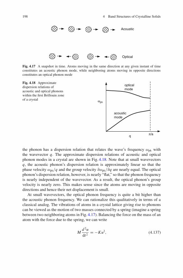
198 4 Band Structures of Crystalline Solids
Acoustic
Optical
Fig. 4.17 A snapshot in time. Atoms moving in the same direction at any given instant of timeconstitutes an acoustic phonon mode, while neighboring atoms moving in opposite directionsconstitutes an optical phonon mode
q
wph
acousticmode
opticalmode
p/a
Fig. 4.18 Approximatedispersion relations ofacoustic and optical phononswithin the first Brillouin zoneof a crystal
the phonon has a dispersion relation that relates the wave’s frequency !ph withthe wavevector q. The approximate dispersion relations of acoustic and opticalphonon modes in a crystal are shown in Fig. 4.18. Note that at small wavevectorsq, the acoustic phonon’s dispersion relation is approximately linear so that thephase velocity !ph=q and the group velocity @!ph=@q are nearly equal. The opticalphonon’s dispersion relation, however, is nearly “flat,” so that the phonon frequencyis nearly independent of the wavevector. As a result, the optical phonon’s groupvelocity is nearly zero. This makes sense since the atoms are moving in oppositedirections and hence their net displacement is small.
At small wavevectors, the optical phonon frequency is quite a bit higher thanthe acoustic phonon frequency. We can rationalize this qualitatively in terms of aclassical analog. The vibrations of atoms in a crystal lattice giving rise to phononscan be viewed as the motion of two masses connected by a spring (imagine a springbetween two neighboring atoms in Fig. 4.17). Balancing the force on the mass of anatom with the force due to the spring, we can write
Md2u
dt2D �Ku2; (4.137)

4.8 Density of States of Phonons and Photons 199
where K is the spring constant, M is the atomic mass, and u is the displacementof the atom from its equilibrium position. The solution of this equation is that thedisplacement varies sinusoidally with time as u � ei!pht , where !ph is the frequencyof the oscillation (or frequency of the phonon). Substituting this solution in theprevious equation, we get
!ph Dp
K=M: (4.138)
The above phenomenological relation shows that the phonon frequency increaseswith the spring constant or stiffness of the spring. An acoustic mode with smallwavevectors corresponds to atoms moving in the same direction with small velocityso that the spring connecting two neighboring atoms is barely stretched and thespring does not appear stiff at all. Such a mode will therefore have a small !ph
which agrees with Fig. 4.18. On the other hand, an optical mode will involve twoneighbors moving in opposite directions, which pulls on the spring and makes itappear stiff. Hence, optical phonons will have higher frequency, which is what wesee in Fig. 4.18.
In a “polar” material like GaAs, which consists of two different types of atoms(Ga and As), any displacement of an atom from its mean position causes local chargepolarization since the two different atoms have different numbers of electrons.Therefore, the phonons in a polar material cause an oscillating electric field tobuild up within the crystal. Such phonons are called polar phonons. In contrast,an elemental semiconductor like Si has only one kind of atom and is therefore“nonpolar” in the sense that atomic vibrations do not cause charge polarizationwithin the crystal. Hence, the phonons in a nonpolar material are nonpolar phonons.
Additionally, a phonon wave has a polarization just as most waves do. If thedisplacement of the vibrating atoms in the crystal is in the same direction inwhich the phonon wave propagates, the polarization is “longitudinal,” whereas ifthe displacement is transverse to the direction in which the wave propagates, thepolarization is “transverse.” The velocity of an acoustic wave traveling througha crystal typically depends on its polarization. Sometimes a wave has mixedpolarizations or other types of complex and exotic polarizations, particularly inquantum-confined structures like a quantum wire. Those are beyond the scope of thisbook, but are discussed in [11]. Suffice it to say then that a phonon has three differentcharacteristics: (1) mode (acoustic or optical), (2) nature (polar or nonpolar), and(3) polarization (longitudinal or transverse). A phonon in a crystal will thereforefall under one of eight different categories characterized by the two types of mode,two types of nature, and two types of polarization. The phonon family is pictoriallydepicted in Fig. 4.19.

200 4 Band Structures of Crystalline Solids
Phonons
Acoustic Optical
Longitudinal LongitudinalTransverse Transverse
Polar Non-polar Polar Non-polar Polar Non-polar Polar Non-polar
Fig. 4.19 The phonon family
4.8.1 Density of Modes or Density of States of Phonons
A phonon in a solid behaves as a plane wave and hence must obey the plane waveequation
r2r u.x; y; z; t/C 1
v2ph
@2u.x; y; z; t/
@t2D 0; (4.139)
where vph is the wave velocity of the phonon.Now consider the fact that the phonon is confined within a crystal of volume L3.
We will think of the crystal as a cube of edge L. Because of this confinement, theamplitude u.x; y; z; t/ must vanish at x D 0; L; y D 0; L and z D 0; L. Withthese boundary conditions, a solution of the wave equation is
u.x; y; z; t/ D A sinnx�x
L
�
sinny�y
L
�
sinnz�z
L
�
sin�
qvpht
; (4.140)
where A is a constant, q is the phonon’s wavevector and nx , ny , and nz are integers.Substitution of this solution into the wave equation immediately yields the
relationnx�
L
�2 Cny�
L
�2 Cnz�
L
�2 D q2: (4.141)
In order to find how many phonon modes are allowed within the crystal, weneed to evaluate how many modes can meet the above condition. This is equivalentto counting all possible combinations of nx , ny , and nz that satisfy (4.141). Thenumber of combinations can be viewed as the volume of a three-dimensionalgrid of the values of n in n-space as shown in Fig. 4.20. This is the so-calledRayleigh scheme of counting modes [12]. In spherical coordinates, this volumeis .4=3/�.n2x C n2y C n2z /
3=2. However, we have to make two corrections to thisvolume. First, in using the sphere in n-space, we have used both positive andnegative values of n, while the wave equation solution admits only positive values.

4.8 Density of States of Phonons and Photons 201
n x
^
ny
nx
nz
n xx ^ n yy
^+ + n zz
Fig. 4.20 Rayleigh schemeof counting modes
Therefore the number of combinations (or, equivalently, the number of allowedphonon modes) is .1=2/3 or 1/8-th of the sphere’s volume and is therefore equalto .1=6/�.n2x Cn2y Cn2z /
3=2. Second, a plane wave can be polarized in two mutuallyperpendicular directions (the longitudinal and transverse phonon modes). Therefore,we have to multiply the reduced volume by two to account for that. Hence, thenumber of phonon modes will be .1=3/�.n2x C n2y C n2z /
3=2. Using (4.141), thisnumber can be written as .1=3/q3L3=�2. Now the volume that this number of modesoccupies in wavevector space or q-space is .4=3/�q3. Hence, the density of modesin q-space is .1=3/q3L3=�2 divided by .4=3/�q3 which is L3=.4�3/ or V=4�3,which is reminiscent of the density of (electron) states in wavevector space. If wethink of phonon modes as phonon states, then the density of states of phonons inwavevector space is equal to the density of states of electrons in wavevector space.
4.8.2 Density of States of Photons
A photon is a quantum of electromagnetic wave just as a phonon is a quantum ofacoustic wave. Even without a detailed derivation, we can see easily that the densityof modes or density of states of photons in wavevector space will be the same asthat of phonons. This follows from the fact that an electromagnetic wave obeys theMaxwell’s equation
r2r E.x; y; z; t/ C �2
[email protected]; y; z; t/
@t2D 0; (4.142)
where E is the electric field in the wave, c is the wave velocity of the photon (i.e., thevelocity of the electromagnetic wave) and � is the refractive index of the medium inwhich the electromagnetic wave is traveling.

202 4 Band Structures of Crystalline Solids
The above equation is identical in mathematical form to (4.139). Therefore,E.x; y; z; t/ has the same solution as (4.140) (with vph replaced by c=�) becausethe boundary conditions are the same. Here, q will be the photon’s wavevector.The rest of the derivation is the same as in the case of phonons. In the end, we getthe result that the density of states of electrons, phonons, and photons are the samein wavevector space.
The last result allows us to calculate the density of state of photons in energyspace or photon frequency space. For this purpose, we use the usual relation(in three dimensions)
Dph.!/d! D Dph.Eq/d3Eq D ˝
4�34�q2dq; (4.143)
which yields
Dph.!/ D ˝q2
�2dq
d!D ˝
!2
�2�3
c3; (4.144)
where we have assumed that the dispersion relation of photons is ! D .c=�/q.
4.9 Summary
In this chapter, we learned four different techniques to calculate an electron’swavefunction and the bandstructure, i.e., energy versus wavevector (E�k) relations,in a crystalline solid. The important points to remember are:
1. In the NFE approach, the electron wavefunction is written as a linear superpo-sition of free electron wavefunctions, i.e., expanded in the basis of free-electronwavefunctions, which are plane waves. Time-independent, nondegenerate, firstorder perturbation theory is applied to calculate the coefficients of expansion,which then yields the complete wavefunction in the crystal as well as the energyversus wavevector relation. This method is most suitable for crystals like sodiumwhere the electron is loosely bound to the parent ion and is therefore nearly free.
2. The opening up of bandgaps at Brillouin zone edges is explained by invokingdegenerate perturbation theory, which also allows us to calculate the bandgapenergies.
3. In the OPW expansion method, the electron’s wavefunction is written as amixture of free electron wavefunctions and atomic orbital wavefunctions. Onceagain, time-independent, nondegenerate, first order perturbation theory is appliedto calculate the complete wavefunction and the bandstructure. This can beachieved in two ways: (1) the direct method, and (2) the pseudopotential method.
4. In the TBA, the electron wavefunction is written as a LCAO wavefunctions. Thecoefficients of expansion are not found from perturbation theory but by assumingthat electrons can tunnel or hop between nearest neighbor atomic sites only, andthen applying the Bloch Theorem to derive a relation between the coefficients.

Problems 203
This approach also directly yields the energy dispersion relation. From the latter,we can derive analytical expressions for the electron velocity and effective massin terms of the tunneling matrix element, which is a measure of how easily anelectron can tunnel between neighboring sites. This is the only nonperturbativeapproach to calculation of bandstructure that we have discussed.
5. In the Ek � Ep perturbation method, we substitute the Bloch expression for theelectron wavefunction in the Schrodinger equation. This yields a Schrodinger-like equation for the Bloch function, where the scalar product Ek � Ep appears asa perturbation term. Time-independent, nondegenerate, first-order perturbationtheory is applied to find the Bloch function and the energy dispersion relations.This technique is very illustrative since it shows clearly the consequences ofneglecting spin–orbit interaction for holes and the perturbation caused by remotebands.
6. The density of states can be expressed in either the wavevector space or inenergy space. The advantage of the former is that in wavevector space, thedensity of states of one-, two-, or three-dimensional structures is independent ofwavevector. In energy space, the density of states of two-dimensional structures isindependent of energy, but this is not true in the case of three- or one-dimensionalstructures.
7. The density of states allows us to calculate carrier concentrations in two- orthree-dimensional systems at any arbitrary temperature. In the case of a one-dimensional structure, we cannot derive compact analytical expressions for thecarrier concentration because the density of states has a singularity at the zero ofenergy. Such a singularity is known as a van Hove singularity.
8. The Fermi energy is determined by the carrier concentration and vice versa.9. The density of states of electrons, phonons, and photons are the same in
wavevector space.
Problems
Problem 4.1. The Fourier transform of the unscreened Coulomb potential V.Er/ De2
4��jErj is given by
VEk0�Ek D 1
˝
Z 1
�1V.Er/d 3Er D 1
˝
e2
4��ˇˇˇEk � Ek0
ˇˇˇ
2;
where � is the dielectric constant of the crystal.Assuming that the lattice potential in a particular crystal is unscreened Coulom-
bic, apply the NFE technique to calculate the value of the lowest energy gap openingup at the so-called L-point in the first Brillouin zone, i.e., at Ek D Œ�=a; �=a; �=a�,where a is the lattice period. The normalizing volume ˝ is equal to the volume

204 4 Band Structures of Crystalline Solids
of the unit lattice, i.e., V D a3. For this problem, assume the following values:a D 0:5 nm and � D 12:9 � 8:854 � 10�12 Farads/meter. Do you expect materialswith larger dielectric constant to have smaller or larger bandgaps? Explain.
Problem 4.2. Using the Bloch Theorem, first derive the following relation for theelectron wavefunction in a crystal:
�Er C nEa D eiEk�nEa .Er/;
where Ea is the lattice constant or lattice period.Show that the OPW basis function �OPW
n .Er/ obeys the above relation andtherefore is a legitimate choice to represent an electron’s wavefunction in a crystal.
Problem 4.3. Bloch–Zener oscillations: According to the simple TBA formalismthat we considered in this chapter, the energy dispersion relation in a single bandcan be expressed as
E.k/ D � � 2t cos.ka/; (4.145)
where t is the tunneling matrix element and a is the lattice constant or lattice period.Consider an electron in a crystal which is subjected to an external (uniform)
electric field EE . Ignore scattering forces. The field exerts a force on the electron,which accelerates the particle according to Newton’s second law:
d.„k/dt
D �e EE : (4.146)
Using (4.145) and (4.146), show that the velocity of the electron will oscillate intime with an angular frequency given by
! D ej EE ja„ : (4.147)
Hint: To show this, you will have to show that the electron’s velocity v in the bandobeys the equation of a simple-harmonic-motion oscillator:
d2v
dt2C
ej EE ja„
!2
v D 0:
Physically explain the cause of this oscillation which is called Bloch–Zeneroscillation. Find the angular frequency in (4.147) if the electric field is 100 kV/cmand the lattice constant is 0.5 nm. It is awfully hard to observe these oscillationsin practice since scattering forces (which we ignored) tend to dephase theseoscillations.
Problem 4.4. Justify the plots in Fig. 4.9 using the 4�4 Hamiltonians in (4.96) and(4.97).

Problems 205
Problem 4.5. Consider the 4�4 Hamiltonian in (4.97) which includes the effect ofremote bands, but ignores spin–orbit interaction.
(a) We wish to find the E � k relation of the three valence bands along the Œ100�and Œ111� crystallographic (Miller) directions. In the former case, kx D k; ky Dkz D 0, and in the latter case, kx D ky D kz D k=
p3. Find the E � k relations
and show that two of the bands are degenerate.(b) The effective mass of holes along the [100] direction was determined experi-
mentally (from cyclotron resonance experiments) and was found to be 0.3m0 inthe doubly degenerate bands and 0.2m0 in the other band (m0 is the free electronmass). Also, the effective mass of the doubly degenerate band along the [111]direction was determined to be 0.5m0. Armed with this knowledge, determinethe effective mass of holes in the three bands along the [110] crystallographicdirection. Are any two bands degenerate (at nonzero wavevector values) alongthe [110] direction?
Problem 4.6. We wish to determine the bandstructure of a hypothetical crystalwhere the effect of remote bands can be neglected for small wavevectors, so thatit is adequately described by the 8�8 Kane matrix.
Plot the E � k relations for small k-values along the [100] direction. For ourhypothetical material, the Luttinger parameters are 1 D 7:65, 2 D 2:41, 3 D 3:28
and the spin–orbit splitting energy�so is 0.34 eV.Concentrate on the lower 6�6 block in the Kane matrix which describes the
valence band. You will find that for the [100] crystallographic direction, this blockdecouples into two 3�3 blocks, which means that the bands are spin-degenerate(spin–orbit coupling does not lift the spin degeneracy). The Kip–Kittel–Dresselhausparameters are related to the Luttinger parameters as
A D „22m0
1
B D „2m0
2
p
C2 C 3B2 D p3
„2m0
3:
(a) Find the dispersion relations of the three valence bands in the [100] direction.(Hint: One of the eigenvalues of the 3�3 block is Ev0 � Bk2 C�so=3.)
(b) You will find that one of the three bands has a parabolic dispersion relation,while the other two do not. Is the parabolic band the heavy-hole, light-hole, orsplit-off band?
(c) Calculate the effective masses of the holes (for motion along the [100] direction)around k D 0.
Problem 4.7. Derive expressions for the three-dimensional density of states asfunctions of energy in the three valence bands that you derived in the previousproblem. Express your answer in terms of the Kip–Kittel–Dresselhaus parameters.

206 4 Band Structures of Crystalline Solids
Problem 4.8. (a) Consider the dispersion relation in (2.131). Find an expressionfor the two-dimensional density of states as function of electron kinetic energyE . Is this independent of kinetic energy?
(b) Consider a quasi two-dimensional electron gas (2-DEG) where the Fermilevel is well below the bulk conduction band edge so that the Boltzmannapproximation to Fermi–Dirac statistics is valid. Show that the equilibriumsheet concentration of electrons in the 2-DEG at any temperature T is
ns D m�kBT
�„2X
n
e�F�EnkBT Œ1C 2˛ .En C kBT /� ;
wherem� is the effective mass, kBT is the thermal energy,�F is the Fermi leveland En is the energy at the bottom of the n-th subband.
(c) By what percentage would you underestimate the equilibrium sheet electronconcentration at room temperature (300 K) in a 100 A wide GaAs quantumwell if you did not account for nonparabolicity? Assume that the effective massis 0.067m0, ˛ D 0:6/eV and the Fermi level is kBT energy below the bulkconduction band edge.
Problem 4.9. (a) Consider a one-dimensional lattice maintained at 0 K tempera-ture. Assume that only the lowest band is filled with electrons since the Fermilevel is below the second lowest band. Show that if there are two electrons peratom, then the energy at the Brillouin zone edge is the Fermi energy EF. Inother words, the Fermi level �F intersects the E � k curve at the Brillouin zoneedge.
(b) Will this crystal be an insulator or a metal? An insulator can carry no currentwhen a voltage is applied across it, while a metal will carry current. Acompletely filled band cannot carry any current since for every electron with awavevector Ck, there is one with wavevector �k and the currents due to thesetwo states cancel.
(c) Assume that the bandstructure has been calculated using the TBA formalismand there is only one electron per atom. Derive an expression for the E � k
relation in terms of the lattice period a and the Fermi energy EF. Assumealso that the energy is zero when the wavevector is zero. Show that the one-dimensional density of states in kinetic energy space is given by
D1�d .Ek/ D 2L
�EFa
q
1 � .Ek=EF � 1/2;
where L is the crystal’s length.(d) At what energies do van-Hove singularities occur, i.e., the one-dimensional
density of state diverges?
Problem 4.10. The heavy-hole, light-hole, and split-off band effective masses in ahypothetical semiconductor are 0.2m0, 0.06m0, and 0.1m0. The valence band topoccurs at k D 0, where the light- and heavy-hole bands are degenerate and the split-
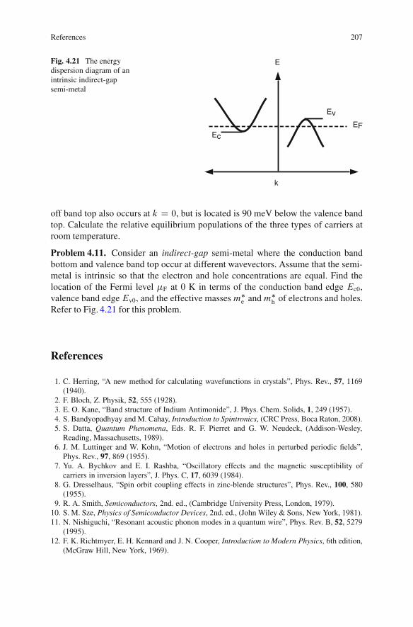
References 207
E
k
EFEc
Ev
Fig. 4.21 The energydispersion diagram of anintrinsic indirect-gapsemi-metal
off band top also occurs at k D 0, but is located is 90 meV below the valence bandtop. Calculate the relative equilibrium populations of the three types of carriers atroom temperature.
Problem 4.11. Consider an indirect-gap semi-metal where the conduction bandbottom and valence band top occur at different wavevectors. Assume that the semi-metal is intrinsic so that the electron and hole concentrations are equal. Find thelocation of the Fermi level �F at 0 K in terms of the conduction band edge Ec0,valence band edge Ev0, and the effective masses m�
e and m�h of electrons and holes.
Refer to Fig. 4.21 for this problem.
References
1. C. Herring, “A new method for calculating wavefunctions in crystals”, Phys. Rev., 57, 1169(1940).
2. F. Bloch, Z. Physik, 52, 555 (1928).3. E. O. Kane, “Band structure of Indium Antimonide”, J. Phys. Chem. Solids, 1, 249 (1957).4. S. Bandyopadhyay and M. Cahay, Introduction to Spintronics, (CRC Press, Boca Raton, 2008).5. S. Datta, Quantum Phenomena, Eds. R. F. Pierret and G. W. Neudeck, (Addison-Wesley,
Reading, Massachusetts, 1989).6. J. M. Luttinger and W. Kohn, “Motion of electrons and holes in perturbed periodic fields”,
Phys. Rev., 97, 869 (1955).7. Yu. A. Bychkov and E. I. Rashba, “Oscillatory effects and the magnetic susceptibility of
carriers in inversion layers”, J. Phys. C, 17, 6039 (1984).8. G. Dresselhaus, “Spin orbit coupling effects in zinc-blende structures”, Phys. Rev., 100, 580
(1955).9. R. A. Smith, Semiconductors, 2nd. ed., (Cambridge University Press, London, 1979).
10. S. M. Sze, Physics of Semiconductor Devices, 2nd. ed., (John Wiley & Sons, New York, 1981).11. N. Nishiguchi, “Resonant acoustic phonon modes in a quantum wire”, Phys. Rev. B, 52, 5279
(1995).12. F. K. Richtmyer, E. H. Kennard and J. N. Cooper, Introduction to Modern Physics, 6th edition,
(McGraw Hill, New York, 1969).

Chapter 5Carrier Scattering in Solids
5.1 Charge Carrier Scattering
An electron (or a hole) moving through any solid encounters random scatterers thatcan change its energy and/or its momentum. A scatterer could be a charged impurityin a crystal lattice (e.g., an ionized donor or acceptor atom), another electron orhole, a phonon which is associated with thermal vibrations of the lattice at a finitetemperature, or anything else that can take the charged carrier from one wavevectorstate to another. Since the wavevector changes (in either magnitude or directionor both), the momentum will change. Additionally, the kinetic energy will changeif the wavevector’s magnitude changes. If the kinetic energy does change, thenthe electron will either absorb energy from the scatterer or emit energy. We willbe interested in finding the rates with which such scattering events or interactionsoccur since they will determine the momentum and energy relaxation rates. Sincethe electron’s wavevector state will change from Ek to Ek0 as a result of scattering, theassociated scattering rate will be denoted as S.Ek; Ek0/. We encountered this quantityin Chap. 2 in the context of the Boltzmann Transport Equation.
5.2 Fermi’s Golden Rule for Calculating CarrierScattering Rates
The prescription for calculating the scattering rate S.Ek; Ek0/ is known as Fermi’sGolden Rule [1, 2]. This rule provides an approximate analytical expression forthe scattering rate and is derived from time-dependent perturbation theory whichwe derived in Chap. 3. Since Fermi’s Golden Rule tells us the rate of transitionof an electron from one wavevector state to another, it has applications beyondscattering theory. For example, it can tell us the rate at which electrons transitionfrom a wavevector state in the valence band of a crystal to another wavevectorstate in the conduction band upon absorption of a photon from a light source.
S. Bandyopadhyay, Physics of Nanostructured Solid State Devices,DOI 10.1007/978-1-4614-1141-3 5, © Springer Science+Business Media, LLC 2012
209

210 5 Carrier Scattering in Solids
k1
k2
ScattererFig. 5.1 An electron with
wavevector Ek1 at time t D 0
interacts with atime-dependent scatterer and
emerges with wavevector Ek2at time t D t
Therefore, it can be used to calculate the absorption coefficient of light in a solidas well. We will see more of that in Chap. 6, but our immediate task is to derive anexpression for S.Ek; Ek0/ using time-dependent perturbation theory. The expressionthat we will derive is Fermi’s Golden Rule.
5.2.1 Derivation of Fermi’s Golden Rule
Consider an electron in a crystal with initial wavevector Ek1 at time t D 0 thatinteracts with a scatterer as shown in Fig. 5.1 and emerges with a wavevectorEk2 at time t D t . In general, the scatterer will be a time-dependent scatterer (e.g.,a phonon or another electron passing by) and therefore it will act as a time-dependent perturbation. Prior to encountering the scatterer, at time t D 0, theelectron was obviously in an eigenstate of the crystal with wavevector Ek1. Hence,
its wavefunction was 1p˝
eiEk1�EruEk1.Er/ in accordance with the Bloch Theorem. Afterinteracting with the scatterer which acts as a time-dependent perturbation, theelectron’s wavefunction will change. The final wavefunction will be a superpositionof all allowed wavevector states Ek. Therefore, the wavefunction at time t D t canbe written as (recall time-dependent perturbation theory of Chap. 3)
.Er; t/ D 1p˝
X
EkCEk.t/e
iEk�EruEk.Er/e�iEEkt=„; (5.1)
where EEk is the energy in wavevector state Ek (found from the E � k relation in thecrystal) and the coefficientCEk.t/ will depend on time because of the time-dependentnature of the scatterer. We will find the latter using standard time-dependentperturbation theory of Chap. 3.
After the scattering event is complete at time t D t , the probability of finding theelectron emerging in the wavevector state Ek2 is, by definition,
P.Ek2/ D jCEk2.t/j2: (5.2)

5.2 Fermi’s Golden Rule for Calculating Carrier Scattering Rates 211
Therefore, the scattering rate S.Ek1; Ek2/, which is nothing but the probability of anelectron initially in state Ek1 ending up in state Ek2 per unit time, is
S.Ek1; Ek2/ D limt!1
P.Ek2/t
D limt!1
jCEk2.t/j2t
: (5.3)
Note that the physical significance of allowing the time t to go to infinity inthe previous equation is that the collision duration is viewed as infinitely long.Therefore, what we will derive—namely Fermi’s Golden Rule—is strictly valid forprolonged interactions and not instantaneous ones. Consequently, Fermi’s GoldenRule should never be applicable in Boltzmann Transport formalism because therescattering events are viewed as instantaneous in both time and space. Yet, in spite ofthis contradiction, the result of Fermi’s Golden Rule is routinely used to calculatescattering rates in Boltzmann transport and in many other situations. To go beyondFermi’s Golden Rule requires considerable effort which is seldom made.
There are, however, many inherent contradictions in Fermi’s Golden Rule. Ifthe collision duration is infinite and the electron is in an electric or magnetic fieldwhen it scatters, then its energy should change immensely while it is scatteringbecause the electric and/or magnetic field will accelerate or decelerate it. This effectis not included in Fermi’s Golden Rule which, as we shall see, does not allowthe electron’s energy to change during scattering events except via emission orabsorption of scattering entities such as phonons. The infinite collision durationis nevertheless consistent with the fact that the electron’s energy before and afterscattering are precisely defined (anything else would have violated the HeisenbergUncertainty Principle). On the other hand, the infinite collision duration also seemsto imply that the mean time between collisions must be infinite since otherwisetwo scattering events have to overlap in time. But an infinite mean time will makethe scattering rate identically zero! Thus, there are many contradictions. Despite allthese bothersome conundrums, Fermi’s Golden Rule has become the most widelyused recipe to calculate scattering rates since it provides an elegant and simpleanalytical expression to calculate the latter.
Going back to standard time-dependent perturbation theory, we note from (3.76)that the coefficients CEk1.t/; CEk2 .t/; : : : CEkn.t/ must obey the equation
i„ @
@t
2
666666664
CEk1.t /
CEk2.t /
: : :
: : :
: : :
CEkn.t /
3
777777775
D
2
666666666664
H 0
Ek1;Ek1.t / H 0
Ek1;Ek2.t /ei
EEk1
�EEk2
„
t � � � H 0
Ek1;Ekn.t /ei
EEk1
�EEkn
„
t
H 0
Ek2;Ek1.t /ei
EEk2
�EEk1
„
t H 0
Ek2;Ek2.t / � � � H 0
Ek2;Ekn.t /ei
EEk2
�EEkn
„
t
: : :
: : :
: : :
H 0
Ekn;Ek1.t /ei
EEkn
�EEk1
„
t H 0
Ekn;Ek2.t /ei
EEkn
�EEk2
„
t � � � H 0
Ekn;Ekn
3
777777777775
2
666666664
CEk1.t /
CEk2.t /
: : :
: : :
: : :
CEkn.t /
3
777777775
:
(5.4)
Hence, this equation must be solved to find the coefficients CEk.t/ that yield theexpression for the scattering rate.
212 5 Carrier Scattering in Solids
Born approximation: We will now have to make an approximation known as theBorn approximation. We will assume that since the scattering potential is weak,it perturbs the electron wavefunction very slightly. As a result, the perturbedwavefunction is only marginally different from the unperturbed wavefunction.Consequently, CEk1.t/ � 1 at all times t and CEkn.t/ � 0 if n ¤ 1. This is known asthe Born approximation. It allows us to ignore terms in every column of the abovematrix except the first, so that we can write
i„@CEk2.t/@t
� H 0Ek2;Ek1.t/e
iE
Ek2�E
Ek1„
t ; (5.5)
where, from (3.75), the matrix element is
H 0Ek2;Ek1.t/ D 1
˝
Z 1
0
d 3Ere�iEk2 �Eru�Ek2.Er/Vs.Er; t/eiEk1�EruEk1.Er/; (5.6)
with Vs.Er; t/ being perturbation term in the Hamiltonian. This term is the space- andtime-dependent scattering potential, which is the potential energy of the scatterer(e.g., phonons, impurities, etc.) responsible for the scattering event.
From (5.5), we obtain
CEk2.t/ � 1
i„Z t
0
H 0Ek2;Ek1.t
0/eiE
Ek2�E
Ek1„
t 0dt 0 C CEk2.0/: (5.7)
The last term on the right-hand side in the above equation is exactly zero sinceat time t D 0, the electron was in state Ek1. Therefore, the probability of finding it instate Ek2 at time t D 0, which is jCEk2.0/j2, is exactly zero. As a result,
CEk2.t/ � 1
i„Z t
0
H 0Ek2;Ek1.t
0/eiE
Ek2�E
Ek1„
t 0dt 0: (5.8)
Next, we will consider time-dependent scattering potentials that vary periodicallyin time and space. Such a potential can be expanded in a Fourier series and viewedas the superposition of forward and backward traveling plane waves. Accordingly,we will write the scattering potential as
Vs.Er; t/ D V Cs .Er; t/C V �
s .Er; t/ DX
!;Eq; OpV C!;Eq; Opei.!t�Eq�Er/ C
X
!;Eq; OpV �!;Eq; Ope�i.!t�Eq�Er/;
(5.9)
where Op is the polarization of the wave, ! is the angular frequency, and Eq is thewavevector.
The first term in the right-hand side is the forward traveling component and thelast term is the backward traveling component. The quantity V C
!;Eq; Op is the Fourier

5.2 Fermi’s Golden Rule for Calculating Carrier Scattering Rates 213
component of the scattering potential at frequency ! and wavevector Eq in theforward traveling wave of polarization Op and V �
!;Eq is the Fourier component of the
scattering potential at frequency! and wavevector Eq in the backward traveling waveof polarization Op.
Let us now focus on one particular polarization Op and one particular Fouriercomponent of the scattering potential with frequency ! and wavevector Eq. Theperturbation Hamiltonian due to this component alone is (from (5.6))
H 0!;Eq; Op;Ek2;Ek1.t
0/ D 1
˝
Z 1
0
d 3Ere�iEk2 �Eru�Ek2.Er/V
C!;Eq; Opei.!t 0�Eq�Er/eiEk1�EruEk1.Er/
C 1
˝
Z 1
0
d 3Ere�iEk2�Eru�Ek2.Er/V
�!;Eq; Ope�i.!t 0�Eq�Er/eiEk1�EruEk1.Er/
D MC!;Eq; Op;Ek2;Ek1e
i!t 0 CM�!;Eq; Op;Ek2;Ek1e
�i!t 0 ; (5.10)
where
M˙!;Eq; Op;Ek2;Ek1 D 1
˝
Z 1
0
d 3Ere�iEk2�Eru�Ek2.Er/V
˙!;Eq; Ope�iEq�EreiEk1�EruEk1.Er/: (5.11)
The quantity V ˙!;Eq; Op is actually an operator and should be treated like one. For
some types of time-dependent scatterers like phonons, it is a simple multiplicativeoperator, while for some other types, it may not be. In the case of photons, it is adifferential operator. This can make a serious difference and has profound physicalconsequences (see Special Topic 2 in Chap. 6). However, if we assume V ˙
!;Eq; Op to bea simple multiplicative operator, then we can simplify the previous equation to
M˙!;Eq; Op;Ek2;Ek1 D
V ˙!;Eq; Op˝
Z 1
0
d 3Ere�iEk2�Eru�Ek2.Er/e
�iEq�EreiEk1�EruEk1.Er/
�V ˙!;Eq; Op˝
Z 1
0
d 3Ere�iEk2�Ere�iEq�EreiEk1�Er Œfor parabolic bands�
D V ˙!;Eq; OpıEk2;Ek1�Eq; (5.12)
where the “delta” is a Kronecker delta.The approximation for parabolic bands (with parabolic E � k relation) is based
on the fact that electron wavefunctions in parabolic bands are plane waves just likethat of a free electron. In other words, the Bloch functions uEk.Er/ become exactlyunity. Note that the Kronecker delta simply represents momentum conservation inthe scattering process („Ek2 D „Ek1 ˙ „Eq).
In very nonparabolic bands, the Bloch functions uEk.Er/ cannot be assumed tobe unity when calculating M˙
!;Eq;Ek2;Ek1 . Additionally, they play an important role in

214 5 Carrier Scattering in Solids
interband scattering, i.e., scattering between two different bands in the Brillouinzone, regardless of whether the band is parabolic or not. The Bloch functions of twostates in two different bands at the same wavevector in the reduced Brillouin zoneare orthogonal. In the extended zone representation, these wavevectors will differby integer multiples of the reciprocal lattice vector EG. Scattering between states indifferent bands are called Umklapp processes and they are rare since they involvea very large momentum change („Eq > �=Ea; Ea Dlattice constant). However, it isclear that the matrix element for Umklapp scattering from one band to another willvanish if the initial and final state wavevectors differ by integral multiples of EG sincethe corresponding Bloch functions will be orthogonal. Therefore, such Umklappprocesses are forbidden. This is an important fact that we will miss if we completelyignore the Bloch functions. For intraband scattering events, however, ignoring theBloch functions will not have any serious consequence as long as the bands are atleast nearly parabolic.
Using (5.10) in (5.8), we obtain
CEk2.t/ D CCEk2 .t/C C�
Ek2.t/; (5.13)
where
C˙Ek2 .t/�
1
i„M˙!;Eq; Op;Ek2;Ek1
eiE
Ek2�E
Ek1˙„!
„
t � 1�
EEk2 �EEk1 ˙ „!�.
„D 1
i„M˙!;Eq; Op;Ek2;Ek1e
i�˙t=2 sin.�˙t=2/�˙t=2
t;
(5.14)
and
�˙ D EEk2 � EEk1 ˙ „!„ (5.15)
Substituting (5.13) and (5.14) in (5.3), we obtain
S.!; Eq; Op; Ek1; Ek2/ D limt!1
P.Ek2/t
D limt!1
jCEk2.t/j2t
D limt!1
8
<
:
ˇˇˇM
C!;Eq; Op;Ek2;Ek1
ˇˇˇ
2
t„2�
sin.�Ct=2/�Ct=2
�2
t2 C
ˇˇˇM�
!;Eq; Op;Ek2;Ek1
ˇˇˇ
2
t„2�
sin.��t=2/��t=2
�2
t2
9
>=
>;
D Cproduct terms: (5.16)
As t ! 1, the term within the square brackets in the above equation becomessharply peaked at �˙ D 0 and begins to resemble a delta-function centered at

5.2 Fermi’s Golden Rule for Calculating Carrier Scattering Rates 215
�˙ D 0. It can therefore be approximated as Aı.�˙/, where the strength A is foundfrom the relation
Z 1
�1
�sin.�˙t=2/�˙t=2
�2
d�˙ D 2�
t� A
Z 1
�1ı.�˙/d�˙ D A: (5.17)
This yields that A D 2�t
. Therefore,
limt!1
�sin.�˙t=2/�˙t=2
�2
D 2�
tı.�˙/: (5.18)
Substituting the last relation in (5.16), we finally get the scattering rate as
S.!; Eq; Op; Ek1; Ek2/ � 2�
„2� ˇˇˇM
C!;Eq; Op;Ek2;Ek1
ˇˇˇ
2
ı.�C/CˇˇˇM
�!;Eq; Op;Ek2;Ek1
ˇˇˇ
2
ı.��/
C product terms
�
D 2�
„ˇˇˇM
C!;Eq; Op;Ek2;Ek1
ˇˇˇ
2
ı.EEk2 �EEk1 C „!/C 2�
„ˇˇˇM�
!;Eq; Op;Ek2;Ek1
ˇˇˇ
2
� ı.EEk2 � EEk1 � „!/C product terms: (5.19)
In deriving the above, we used the fact that ı.ax/ D 1jaj ı.x/.
Now, the product terms are comparatively negligible since the first term of theproduct would have been peaked around EEk2 D EEk1 C „!, while the second wouldhave been peaked around a different energyEEk2 D EEk1 �„!. Therefore, the productis negligible as long as „! ¤ 0. Consequently, we can write
S.!; Eq; Op; Ek1; Ek2/ � SC.!; Eq; Op; Ek1; Ek2/C S�.!; Eq; Op; Ek1; Ek2/; (5.20)
where
S˙.!; Eq; Op; Ek1; Ek2/ D 2�
„ˇˇˇM
˙!;Eq; Op;Ek2;Ek1
ˇˇˇ
2
ı.EEk2 �EEk1 ˙ „!/: (5.21)
In a parabolic band, we can use (5.12) to write the above as
S˙.!; Eq; Op; Ek1; Ek2/ D 2�
„ˇˇˇV
˙!;Eq; Op
ˇˇˇ
2
ıEk2;Ek1�Eqı.EEk2 � EEk1 ˙ „!/: (5.22)
Because of the Dirac delta and the Kronecker delta in the preceding equation, therate SC.!; Eq; Op; Ek1; Ek2/ in (5.20) is nonzero only when EEk2 D EEk1 � „! and Ek2 DEk1 � Eq, while the rate S�.!; Eq; Op; Ek1; Ek2/ is nonzero only when EEk2 D EEk1 C „!

216 5 Carrier Scattering in Solids
and Ek2 D Ek1 C Eq. In the first case, the final energy is the initial energy minusthe energy of the scatterer (e.g., phonon) and the final momentum is the initialmomentum minus the momentum of the scatterer. In the second case, the finalenergy is the initial energy plus the energy of the scatterer and the final momentumis the initial momentum plus the momentum of the scatterer. Energy and momentumconservations imply that the first case corresponds to emission of a scattererof energy „! and momentum „Eq (since the electron’s energy and momentumdecrease by these amounts after scattering), while the second case corresponds toabsorption of the scatterer (since the electron’s energy and momentum increase bythese amounts after scattering). Thus, a time varying scattering potential can causescattering by either emission or absorption. The total scattering rate, given in (5.20),is the sum of the emission and the absorption rates.
Equation (5.21) is the final expression that we sought for the scattering rate(either emission or absorption). This expression is referred to as Fermi’s GoldenRule. It tells us what the rate of transition from wavevector state Ek1 to wavevectorstate Ek2 is due to any type of perturbation (phonons, photons, etc.). Note also thatFermi’s Golden Rule automatically enforces energy conservation by means of theDirac delta function, while the matrix element incorporates momentum conservationby means of the Kronecker delta function. The Dirac delta, however, implies thatenergy states before and after scattering are precisely defined. This, in turn, requiresthe collision duration to be infinite in order to satisfy Heisenberg’s UncertaintyPrinciple.
The energy conserving Dirac delta function in Fermi’s Golden Rule tells ussomething else which is important. If the scattering potential Vs.Er; t/ does notdepend on time, then according to (5.9), ! D 0. In that case, EEk2 D EEk1 , whichmeans that the scattering will be elastic. Thus, time-independent scatterers, whichdo not change with time (e.g., a crystallographic defect), can only cause elasticscattering where the electron’s energy before and after scattering remains the same.Inelastic scattering events invariably require a time-dependent scatterer.
5.3 Dressed Electron States and Second QuantizationOperators
In (5.6), we used the “bare” electron states in a crystal j�barei D 1p˝
eiEk�EruEk.Er/to calculate the perturbation term H 0
Ek2;Ek1.t/. However, we now know that this
perturbation causes emission and absorption of entities with energy „!. Emissioncreates these entities and absorption annihilates them. This immediately tells us thatthese entities must be bosons and not fermions, since fermions cannot be created ordestroyed at will, at least in low-energy physics.
Because of the presence of these bosons, we should use “dressed” electronstates instead of the bare electron states to calculate H 0
Ek2;Ek1.t/. Dressed states are

5.3 Dressed Electron States and Second Quantization Operators 217
coupled electron-boson states describing an electron dressed with bosons. Whenwe use them, we automatically account for the possibility that transitions betweensuch states can cause emission or absorption of a boson. Thus, we should use
dressed states j�dressedi D 1p˝
eiEk�EruEk.Er/jN!1;Eq1; Op1 ; N!2;Eq2; Op2 ; N!3;Eq3; Op3 ; : : : i whichrepresents an electron state dressed with N!1;Eq1; Op1 number of bosons (of frequency!1, wavevector Eq1, and polarization Op1), N!2;Eq2; Op2 number of bosons (of frequency!2, wavevector Eq2 and polarization Op2), etc. The quantity N!;Eq; Op is the effectivenumber of bosons in the mode with frequency !, wavevector Eq and polarization Op.This number, however, does not have to be an integer; it can be a fraction or a mixednumber. It is quite possible that one-half of a boson, or three and three-fifths of aboson, occupies a mode. This number is a measure of the likelihood that a modeis occupied. Obviously if there are 3.6 bosons in mode A and 0.5 bosons in modeB, then there is a 7.2 times higher probability for a boson to occupy mode A thanmode B.
Recall that the scattering potential in (5.9) is actually an operator where the firstterm will lead to emission of bosons and the second term will lead to absorption ofbosons. Hence, if we want to write it properly, then we should not write it as a meremultiplicative constant, but instead write it as
Vs.Er; t/ DX
!;Eq; OpV C!;Eq; Opa
�
!;Eq; Opei.!t�Eq�Er/ CX
!;Eq; OpV �!;Eq; Opa!;Eq; Ope�i.!t�Eq�Er/; (5.23)
where the operator a�!;Eq; Op acting on a dressed state will “create” a boson of frequency
!, wavevector Eq and polarization Op because of emission, while the operator a!;Eq; Opwill “annihilate” a boson of frequency !, wavevector Eq, and polarization Op becauseof absorption. These operators are called creation and annihilation operators,respectively. They are also called Bose operators or second quantization operatorssince they are associated with quantization of the boson field.
When these operators operate on a dressed state, they will create or annihilate aboson in that state. This is expressed via the relations:
a�
!n;Eqn; Opn1p˝
eiEk�EruEk.Er/jN!1;Eq1; Ep1 ; N!2;Eq2; Ep2 ; : : : ; N!n;Eqn; Opn ; : : : i
Dq
N!n;Eqn; Opn C 11p˝
eiEk�EruEk.Er/jN!1;Eq1; Ep1 ; N!2;Eq2; Ep2 ; : : : ; N!n;Eqn; Opn C 1; : : : i
(5.24)
a!n;Eqn; Opn1p˝
eiEk�EruEk.Er/jN!1;Eq1; Ep1 ; N!2;Eq2; Ep2 ; : : : ; N!n;Eqn; Opn ; : : : i
Dq
N!n;Eqn; Opn1p˝
eiEk�EruEk.Er/jN!1;Eq1; Ep1 ; N!2;Eq2; Ep2 ; : : : ; N!n;Eqn; Opn � 1; : : : i:(5.25)

218 5 Carrier Scattering in Solids
The above two equations show that the number of bosons (of the rightfrequency !, wavevector Eq, and polarization Op) increases or decreases by onein the dressed state when we operate with creation and annihilation operators,respectively. Note from the above equations that the dressed state j�dressedi D1p˝
eiEk�EruEk.Er/jN!1;Eq1; Ep1 ; : : : ; N!n;Eqn; Opn ; : : : i is not an eigenstate of either the creation
operator a� or the annihilation operator a. Also, neither ispN!n;Eqn; Opn an eigenvalue
of the annihilation operator a!n;Eqn; Opn , nor ispN!n;Eqn; Opn C 1 an eigenvalue of the
creation operator a�!n;Eqn; Opn . It can be shown that these two operators are indeed
hermitian conjugates of each other. Since a� ¤ a, clearly these operators are nothermitian. Second quantized operators do not have to be hermitian since theireigenvalues, if any, do not represent the expectation value of any observable.
We can write (5.25) in short-hand notation as
a�
!n;Eqn; Opn j : : : ; N!n;Eqn; Opn ; : : : i Dq
N!n;Eqn; Epn C 1j : : : ; N!n;Eqn; Epn C 1; : : : i
a!n;Eqn; Epn j : : : ; N!n;Eqn; Epn ; : : : i Dq
N!n;Eqn; Epn j : : : ; N!n;Eqn; Epn � 1; : : : i; (5.26)
where j : : : ; N!n;Eqn; Epn ; : : : i�j�dressediD 1p˝
eiEk�EruEk.Er/jN!1;Eq1; Ep1 ; : : : ; N!n;Eqn; Epn ; : : : i.Applying the above operation rules twice, we get
a�
!n;Eqn; Opna!n;Eqn; Opn j : : : ; N!n;Eqn; Opn ; : : : i D N!n;Eqn; Opn j : : : ; N!n;Eqn; Opn ; : : : i; ora�
!n;Eqn; Opna!n;Eqn; Opn j�dressedi D N!n;Eqn; Opn j�dressedi (5.27)
In this case, the dressed state j�dressedi D j : : : ; N!n;Eqn; Opn ; : : : i is indeed an eigenstate
of the product operator a�!n;Eqn; Opna!n;Eqn; Opn , whose eigenvalue is N!n;Eqn; Opn . Therefore,
this product operator is called the “number operator” since N!n;Eqn; Opn is the numberof bosons in the dressed state.
Using (5.26), we can easily show that
a!n;Eqn; Opna�
!n;Eqn; Opn � a�!n;Eqn; Opna!n;Eqn; Opn D 1; (5.28)
or, in commutator notation,h
a!n;Eqn; Epn ; a�
!n;Eqn; Epni
D 1. This is the universal com-
mutation rule for Bose operators and it shows that the creation and annihilationoperators for bosons do not commute.
5.3.1 Matrix Elements with Dressed States
If we correctly use dressed states instead of bare electron states to calculate thematrix elements for the perturbation Hamiltonian, then (5.10) and (5.12) will bemodified to

5.4 Applying Fermi’s Golden Rule to Calculate Phonon Scattering Rates 219
H 0!;Eq; Op;Ek2;Ek1.t
0/ DpN!;Eq; Op C 1
˝
Z 1
0
d 3Ere�iEk2�Eru�Ek2.Er/V
C!;Eqe
i.!t 0�Eq�Er/eiEk1�EruEk1.Er/
CpN!;Eq; Op˝
Z 1
0
d 3Ere�iEk2�Eru�Ek2.Er/V
�!;Eqe
�i.!t 0�Eq�Er/eiEk1�EruEk1.Er/
D MC!;Eq; Op;Ek2;Ek1e
i!t 0 CM�!;Eq; Op;Ek2;Ek1e
�i!t 0 ; (5.29)
where
M˙!;Eq; Op;Ek2;Ek1 D
V ˙!;Eq; Op˝
q
N!n;Eqn; Epn C .1=2/˙ .1=2/
�Z 1
0
d 3Ere�iEk2�Eru�Ek2.Er/e
�iEq�EreiEk1�EruEk1.Er/: (5.30)
For parabolic bands, the Bloch functions are unity, so that
M˙!;Eq; Op;Ek2;Ek1 D
V ˙!;Eq; Op˝
q
N!n;Eqn; Epn C .1=2/˙ .1=2/
Z 1
0
d 3Ere�iEk2�Ere�iEq�EreiEk1�Er
D V ˙!;Eq; Op
q
N!n;Eqn; Epn C .1=2/˙ .1=2/ıEk2;Ek1�Eq: (5.31)
In deriving the above, we used the orthonormality property of the dressed states:
h: : : ;M!;Eq; Op; : : : j : : : ; N!;Eq; Op; : : : i: D ıM!;Eq; Op;N!;Eq; Op; (5.32)
where the delta is a Kronecker delta.Equation (5.22) should now be modified to
S˙.!; Eq; Op; Ek1; Ek2/ D 2�
„�
N!n;Eqn; Epn C .1=2/˙ .1=2/
�ˇˇˇV ˙!;Eq; Op
ˇˇˇ
2
ıEk2;Ek1�Eqı�
EEk2 �EEk1 ˙ „!�
: (5.33)
5.4 Applying Fermi’s Golden Rule to Calculate PhononScattering Rates
One of the major causes of electron scattering in a crystal, particularly at roomtemperature, is due to interactions of the electron with the oscillating host lattice.The oscillations cause a disturbance that propagates through a bulk crystal like aplane wave. A “phonon” is a quantum of this wave or lattice vibration. Hence, thistype of scattering is simply called phonon scattering.

220 5 Carrier Scattering in Solids
hwphphonon stimulating
phonon
Absorption Stimulatedemission
Spontaneous emission
Rate = CN(wph) Rate = CN(wph) Rate = C
Fig. 5.2 The three different phonon scattering processes. Absorption and stimulated emissionrequire the presence of phonons to absorb or stimulate emission. Hence their rates are proportionalto the phonon occupation probability N.!ph/. Spontaneous emission does not require the presenceof other phonons
The displacement of an oscillating atom from its mean position is periodic intime and space. Hence, it can be expressed as a Fourier series:
u.Er; t/ DX
!ph;Eq
h
AC!ph;Eqei.!pht�Eq�Er/ C A�
!ph;Eqe�i.!pht�Eq�Er/i ; (5.34)
where !ph is phonon frequency and Eq is phonon wavevector.In a parabolic band, we can use (5.33) to find the electron–phonon scattering
rate (for both emission and absorption of a phonon of frequency !ph, wavevector Eqand polarization Op), as long as we can find the Fourier components V ˙
!ph;Eq; Op of the
scattering potential. Our next task is to find V ˙!ph;Eq; Op , but before we do that, let us
digress for a moment and discuss something else.As we have already seen, phonon scattering will cause an electron to either
absorb energy and momentum from the lattice vibration (phonon absorption), orgive up some of its own energy and momentum to the lattice (phonon emission).The latter process (emission) can be of two types: spontaneous and stimulated. Inthe former type, an electron spontaneously emits a phonon and loses energy andmomentum. In the latter type, a second phonon stimulates the electron to emit aphonon. Thus, there are really three different types of electron–phonon scatteringprocesses—absorption, stimulated emission, and spontaneous emission. All threeare pictorially depicted in Fig. 5.2.
From (5.33) it is clear that the absorption rate is proportional to N!ph;Eq; Op , whilethe emission rate is proportional to N!ph;Eq; Op C1. Since absorption requires a phononof frequency !ph, wavevector Eq and polarization Op to be available for absorption,it stands to reason that the absorption rate will be proportional to the number ofphonons available in that mode, i.e., the quantityN!ph;Eq; Op . Hence, this makes perfectsense.
Similarly, stimulated emission requires a phonon of frequency !ph, wavevectorEq, and polarization Op to be available to stimulate an electron to emit a phonon.

5.4 Applying Fermi’s Golden Rule to Calculate Phonon Scattering Rates 221
E2, N2
E1, N1
hω
Fig. 5.3 A two-level systemwith energies E1 and E2 andcarrier populations N1 andN2, respectively
Therefore, the stimulated emission rate should be proportional to N!ph;Eq; Op aswell. That leaves spontaneous emission which does not require any phonon to beavailable. Hence, out of the total emission rate which is proportional toN!ph;Eq; Op C1,the stimulated rate must be proportional to N!ph;Eq; Op and the spontaneous rate mustbe proportional to 1. Next, we show that all this is consistent with thermodynamics.
5.4.1 Einstein’s Thermodynamic Balance Argument
The quantityN.!; Eq; Op/ (sometimes referred to as the “boson occupation number”)can be thought of as the number of bosons occupying the mode with frequency !,wavevector Eq and polarization Op. If the boson system is in thermal equilibrium, thenat any temperature T , this quantity is given by the Bose–Einstein factor:
N.!; Eq; Op/ˇˇequilibrium D 1
e„!kBT � 1
: (5.35)
Note that the equilibrium boson occupation number depends only on the frequency!, or equivalently the energy of the particle „!, and does not depend on thewavevector or polarization. Note also that unlike the Fermi–Dirac factor whichinvolves a Fermi level�F, the Bose–Einstein factor does not involve a correspondingBose level�B. This happens because fermions are conserved (they cannot be createdor destroyed at will; at least in low energy physics), but bosons can be createdor destroyed easily (as in phonon emission or phonon absorption). Only particleswhose numbers are conserved have an energy like the Fermi energy, while particleswhose numbers are not conserved cannot have any such energy. Note also thatN.!; Eq; Op/ can vary between zero and infinity, unlike the Fermi–Dirac factor, which,being an occupation “probability,” is bounded by 0 and 1.
Consider now the two-level system shown in Fig. 5.3 which consists of twoenergy levels E2 and E1. The electron population in level 1 is N1 and that in level 2is N2. Each level’s equilibrium occupation probability is assumed to be determinedby Boltzmann’s statistics so that
N1
N2D e
E2�E1kBT : (5.36)

222 5 Carrier Scattering in Solids
If E2 � E1 D „!, then electrons can transition between the levels by emitting orabsorbing bosons of energy „!. Under thermodynamic equilibrium conditions, therate N2=�21 at which electrons transition from level 2 to level 1 by stimulated andspontaneous emission must equal the rateN1=�12 at which electrons transition fromlevel 1 to level 2 by absorption. This implies
1=�21
1=�12D N1
N2D e
E2�E1kBT D e
„!kBT D
1
e„!kBT �1
C 1
1
e„!kBT �1
D N.!/C 1
N.!/: (5.37)
Therefore, the total emission rate (1=�21) must be proportional to N.!/ C 1 ifthe absorption rate (1=�12) is proportional to N.!/. Since the emission has twocomponents—stimulated and spontaneous—and the former is proportional toN.!/,the ratio of the stimulated and spontaneous rates (and hence the ratio of their squaredmatrix elements) must be proportional to N.!/.
Returning to (5.33), we see that the Kronecker delta function basically enforcesmomentum conservation so that
„Ekfinal D „Ekinitial � „Eq .for emission/„Ekfinal D „Ekinitial C „Eq .for absorption/: (5.38)
All that is left for us to do now in order to evaluate phonon scattering rates is to findthe quantity V ˙
!;Eq; Op
5.4.1.1 Determination of V ˙!;Eq; Op
Let us now focus on just acoustic phonons and determine their V ˙!;Eq; Op . Acoustic
phonons are quanta of acoustic waves in a crystal that carry sound and heatwaves via lattice vibrations. They make the lattice constant Ea oscillate in timeand space because the lattice is continuously expanding and shrinking. Recall fromthe previous chapter that the bandgap of a crystal depends on the lattice constant.Therefore, if the lattice constant is oscillating in time and space, the bandgap of thecrystal will oscillate in time and space as shown in Fig. 5.4. As a result, an electron inthe conduction band of a crystal will experience an oscillating electrostatic potentialof amplitude Ec.Er; t/=2 which acts as a scattering potential. We can expand thispotential in a Fourier series and write:
Ec.Er; t/ DX
!ph;EqEC
c .!ph; Eq/ei.!pht�Eq�Er/ CX
!ph;EqE�
c .!ph; Eq/e�i.!pht�Eq�Er/: (5.39)
If the atoms are not displaced too far from their equilibrium positions, theirvibrations about the equilibrium positions can be viewed as simple harmonic motion

5.4 Applying Fermi’s Golden Rule to Calculate Phonon Scattering Rates 223
Conduction band Ec
Valence band Ev
ΔEc
Fig. 5.4 The conduction and valence band edges in a crystal oscillate in time and space as thelattice constant oscillates because of phonons
resulting in longitudinally polarized and transversely polarized acoustic wavestraveling through the crystal. In the valley of a semiconductor, the transversemodes (or more precisely the shear strains associated with transverse modes)produce no energy modulation in the conduction band or valence band, althoughin L or X valleys, they can [3]. Accordingly,Ec.Er; t/ D 0 for transverse acousticphonons in the valley. Therefore, if we just restrict ourselves to the valley, thenwe can write:
ˇˇˇV
˙!;Eq; Op
ˇˇˇ
2 Dˇˇˇˇ
Ec .!ph; Eq/2
ˇˇˇˇ
2
Op � Eqjqj ; (5.40)
where Op is the polarization vector (of unit norm) of the phonon wave and Eqis the phonon wavevector. Note that the scalar product vanishes for transversephonon modes (because Op and Eq are mutually perpendicular) and becomes unityfor longitudinal phonon modes.
5.4.1.2 Nonpolar Longitudinal Acoustic Phonons
For nonpolar acoustic phonons, Ec is determined by the spatial rate of displace-ment of the atoms from their mean position and is given by [3]
Ec.Er; t/ D D Err � Eu.Er; t/; (5.41)
whereD is the so-called dilational deformation potential and Eu is the displacementof the atoms from their mean position. Since we are dealing with longitudinalphonons, Eq and Eu are collinear. Therefore, using (5.34) for Eu, we get from (5.39)
Ec .!ph; Eq/ D �DiqA˙!ph ;Eq: (5.42)
As a result,
ˇˇˇV ˙!;Eq; Op
ˇˇˇ
2 Dˇˇˇˇ
Ec .!ph; Eq/2
ˇˇˇˇ
2
DD2q2
�
A˙!ph;Eq
�2
4: (5.43)

224 5 Carrier Scattering in Solids
Next, we need to determine A˙!ph;Eq . For this purpose, we invoke conservation of
energy. The kinetic energy of atomic motion is 12Matomjvatom.Er; t/j2, where Matom
is the atom’s mass and vatom.Er; t/ is the (position- and time-dependent) oscillationvelocity of the vibrating atom. We set the kinetic energy of all the atoms in thecrystal equal to the phonon’s energy to obtain
X
crystal
1
2Matomjvatom.Er; t/j2 D 1
2�˝jvatom.Er; t/j2 D „!ph; (5.44)
where � is the mass density and˝ is the volume of the crystal. Now,
vatom.Er; t/Ddu.Er; t/dt
D i!phAC!ph;Eqei.!pht�Eq�Er/.forward traveling wave/
D �i!phA�!ph;Eqe�i.!pht�Eq�Er/.backward traveling wave/;
(5.45)
which yields that for both forward and backward traveling waves
jvatom.Er; t/j2 D !2ph
�
A˙!ph;Eq
�2
.independent of r and t/: (5.46)
Substitution of the last result in (5.44) yields
�
AC!ph;Eq
�2 D�
A�!ph;Eq
�2 D 2„˝�!ph
: (5.47)
Finally, since acoustic phonons have a nearly linear dispersion relation atsufficiently low phonon energies and wavevectors, we can write that !ph D vlq,where vl is the velocity of the longitudinal acoustic phonons, or the longitudinalvelocity of sound propagation in the crystal (not to be confused with vatom).
Normally, this velocity is given by vl Dq
C11�
, where C11 is one of the elastic
constants in the crystal [7]. From (5.40), (5.43) and (5.47), we get
ˇˇˇV ˙!;Eq; Op
ˇˇˇ
2 D D2q„2�vl˝
: (5.48)
For low-energy phonons such that kBT � „!ph,
N.!ph/ˇˇequilibrium D 1
e„!phkBT � 1
� kBT
„!ph: (5.49)

5.4 Applying Fermi’s Golden Rule to Calculate Phonon Scattering Rates 225
Φ
kinitial
kfinalq
Φ
kinitial
kfinalq
Absorption Emission
θ
π−θ
Fig. 5.5 Conservation of momentum in electron–phonon scattering process
This result is sometimes referred to as equipartition of energy since the totalavailable thermal energy kBT is equally divided betweenN.!ph/ phonons such thateach phonon’s energy „!ph is kBT=N.!ph/.
Using this result and (5.48) in (5.33), we get that for low-energy longitudinalnonpolar acoustic phonons
S�.!ph; Eq; Ek1; Ek2/ D 2�
„D2q„2�vl˝
kBT
„!phıEk2;Ek1CEqı
�
EEk2 �EEk1 � „!�
D �D2kBT
„�v2l˝ıEk2;Ek1CEqı
�
EEk2 �EEk1 � „!�
for absorption
SC.!ph; Eq; Ek1; Ek2/ D 2�
„D2q„2�vl˝
kBT
„!phıEk2;Ek1�Eqı
�
EEk2 � EEk1 C „!�
D �D2kBT
„�v2l˝ıEk2;Ek1�Eqı
�
EEk2 � EEk1 C „!�
for stimulated emission
SC.!ph; Eq; Ek1; Ek2/ D 2�
„D2q„2�vl˝
ıEk2;Ek1�Eqı�
EEk2 �EEk1 C „!�
D �D2q„„�vl˝
ıEk2;Ek1�Eqı�
EEk2 � EEk1 C „!�
for spontaneous emission: (5.50)
5.4.1.3 Angular Dependence of Scattering Probability
A phonon scattering event will change a carrier’s wavevector. In Fig. 5.5, weshow the angle ˚ between the initial and final wavevectors, i.e., the wavevectorsbefore and after scattering. Conservation of momentum in the scattering process(represented by (5.38) leads to Fig. 5.5. Obviously, the angle of scattering ˚

226 5 Carrier Scattering in Solids
depends on the wavevector Eq of the phonon that is absorbed or emitted in thescattering process. The larger the magnitude of Eq, the larger is the angle ˚ .From (5.50), we find that the squared matrix element for absorption or stimulatedemission is independent of q and therefore must be independent of the scatteringangle˚ . This means that absorption and stimulated emission are isotropic scatteringprocesses whose probabilities are independent of the scattering angle. However,the squared matrix element for spontaneous emission is directly proportional to q.Consequently, stimulated emission is an anisotropic scattering process and there isa clear preference for scattering through larger angles. Such a scattering processis extremely efficient in relaxing the electron’s momentum since it changes thedirection of momentum by a lot. Therefore, spontaneous emission of nonpolarlongitudinal acoustic phonons degrades an electron’s mobility in a crystal veryefficiently.
5.4.1.4 Polar Longitudinal Acoustic Phonons
Polar acoustic phonons are associated with time- and space-varying local chargepolarization within a polar material (like GaAs) that occur due to lattice vibrations ofatoms. Since the bond between two atoms is polar, displacement of the atoms fromtheir mean positions causes charge build up in the crystal and an associated electricfield. This phenomenon is the cause of piezoelectricity; hence, an electron scatteringevent mediated by longitudinal polar acoustic phonons is also often referred to aspiezoelectric scattering.
The time- and space-varying charge polarization gives rise to an electric fieldwhich propagates as a wave through the crystal. The Fourier component of thelongitudinal mode with frequency !ph and wavevector Eq can be written as
EE!ph;Eq.Er; t/ D EC!ph;Eqei.!pht�Eq�Er/ Oq C E�
!ph;Eqe�i.!pht�Eq�Er/ Oq; (5.51)
where Oq is the unit vector in the direction of the wavevector.The electric potential associated with the electric field in the direction of the
wavevector is given by
V.Er; t/ D �Z
EE!ph;Eq.Er; t/ � dEr: (5.52)
The modulation in the conduction band edge as a result of this potential is simply
Ec.Er; t/ D �eV.Er; t/: (5.53)
Hence, from the last three equations and (5.39), we get
Ec .!ph; Eq/ D ˙eE˙!ph;Eqiq
: (5.54)

5.4 Applying Fermi’s Golden Rule to Calculate Phonon Scattering Rates 227
Therefore, for longitudinal polar acoustic phonon interaction,
ˇˇˇV
˙!;Eq; Op
ˇˇˇ
2 Dˇˇˇˇ
Ec .!ph; Eq/2
ˇˇˇˇ
2
De2ˇˇˇE˙!ph;Eq
ˇˇˇ
2
4q2; (5.55)
so that, from (5.33), we get
S�.!ph; Eq; Ek1; Ek2/ D 2�
„ N.!ph/e2ˇˇˇE�!ph;Eq
ˇˇˇ
2
4q2ıEk2;Ek1CEqı
�
EEk2 � EEk1 � „!�
for absorption
SC.!ph; Eq; Ek1; Ek2/ D 2�
„ N.!ph/e2ˇˇˇEC!ph;Eq
ˇˇˇ
2
4q2ıEk2;Ek1�Eqı
�
EEk2 �EEk1 C „!�
for stimulated emission
SC.!ph; Eq; Ek1; Ek2/ D 2�
„e2ˇˇˇEC!ph;Eq
ˇˇˇ
2
4q2ıEk2;Ek1�Eqı
�
EEk2 �EEk1 C „!�
for spontaneous emission: (5.56)
For low acoustic phonon energies, when kBT � „!ph, N.!ph/ � kBT=„!ph� D kBT= .„vlq/ [equipartition of energy]. Therefore, the scattering rates for
electron interaction with longitudinal polar acoustic phonons is
S�.!ph; Eq; Ek1; Ek2/ D�e2
ˇˇˇE�!ph;Eq
ˇˇˇ
2
2„vlq3ıEk2;Ek1CEqı
�
EEk2 � EEk1 � „!�
for absorption
SC.!ph; Eq; Ek1; Ek2/ D�e2
ˇˇˇEC!ph;Eq
ˇˇˇ
2
2„vlq3ıEk2;Ek1�Eqı
�
EEk2 �EEk1 C „!�
for stimulated emission
SC.!ph; Eq; Ek1; Ek2/ D�e2
ˇˇˇEC!ph;Eq
ˇˇˇ
2
2„q2 ıEk2;Ek1�Eqı�
EEk2 �EEk1 C „!�
for spontaneous emission: (5.57)
5.4.1.5 Angular Dependence
Note that the matrix elements for absorption and stimulated emission are inverselyproportional to q3 while the matrix element for spontaneous emission is inversely

228 5 Carrier Scattering in Solids
proportional to q2. Recalling Fig. 5.5, it becomes obvious that electron-longitudinalpolar acoustic phonon scattering is extremely anisotropic and there is a strongpreference for scattering through small angles. Such scattering events will notchange the direction of the electron’s wavevector or momentum drastically sincethe angle ˚ between the initial and final directions will be small. Therefore,scattering events mediated by longitudinal polar acoustic phonons—also known aspiezoelectric scattering events—are not very effective in relaxing momentum andconsequently will not degrade the electron mobility in a material significantly.
5.5 Calculation of Relaxation Rates
In MC simulations and in many other situations, we are interested in the totalelectron scattering rate due to one type of scattering (e.g., scattering due tolongitudinal nonpolar acoustic phonons). This quantity is given by
1
�.!ph; Ek/DX
Ek0
S.!ph; Ek; Ek0/: (5.58)
It depends on the initial wavevector and is found by summing S.!ph; Ek; Ek0/ over all
final wavevector states Ek0.We will evaluate this quantity for acoustic phonon scattering in three-, two-,
and one-dimensional structures to illustrate several important properties of carrierscattering in solids. This exercise is very instructive since it brings out manyinteresting and intriguing features that have nontrivial consequences. We will notdo this for every possible type of scattering mechanism since this is a textbook andnot an encyclopedia. If the reader can understand the method for acoustic phononscattering, he/she should be able to repeat the derivation for any other type ofscattering mechanism.
5.5.1 Scattering Rates in 3-D (Bulk) Systems
In a bulk (or three-dimensional) system, the total scattering rate will be
1
�3D.!ph; Ek/DX
Ek0
S.!ph; Ek; Ek0/: (5.59)
where, once again, the upper sign stands for emission and the lower for absorptionof a phonon. Recall that Ek0 is the final state wavevector and Ek is the initial statewavevector. In 3-D, the summation is carried out over the magnitude, polar angle,and azimuthal angle of the final state wavevector (in spherical coordinates).

5.5 Calculation of Relaxation Rates 229
5.5.1.1 Nonpolar Longitudinal Acoustic Phonon Absorption
Using the matrix element for nonpolar longitudinal acoustic phonon absorption(NPLAPA), we find that the scattering rate for this type of interaction is
1
�3D.!ph; Ek/
ˇˇˇˇˇNPLAPA
DX
Ek0
�D2kBT
„�v2l˝ıEk0;EkCEqı.EEk0
� EEk � „!ph/; (5.60)
as long as the phonon energy is much smaller than the thermal energy kBT and thephonons are in equilibrium (so that equipartition of energy holds).
If we now assume that the energy dispersion relation of electrons in the materialis parabolic, and that of acoustic phonons is linear (!ph D „vlq), then
EEk0
D „2k02
2m�
EEk D „2k22m�
„!ph D „vlq: (5.61)
In (5.60), we can absorb the Kronecker delta in the Dirac delta in the followingway. The Kronecker delta yields (see (5.38))
Ek0 D Ek C Eq so thatk02 D Ek0 � Ek0 D .Ek C Eq/ � .Ek C Eq/ D k2 C q2 C 2kq cos �; (5.62)
where � is the angle between Ek and Eq. We use this relation to rewrite the argumentof the Dirac delta function as
EEk0
�EEk � „!ph D „2k02
2m� � „2k22m� � „vlq
D „2q22m� C „2kq cos �
m� � „vlq: (5.63)
Therefore,
ıEk0;EkCEqı
EEk0
�EEk � „!ph� D ı
�„2q22m� C „2kq cos �
m� � „vlq
: (5.64)
Using the last result in (5.60), we obtain
1
�3D.Ek/
ˇˇˇˇˇNPLAPA
DX
Ek0
�D2kBT
„�v2l˝ı
�„2q22m� C „2kq cos �
m� � „vlq
: (5.65)

230 5 Carrier Scattering in Solids
The summation in the right-hand side is over the variable k0, � , and � (where� and � are polar and azimuthal angles of Ek0), but the quantity to be summedover does not explicitly contain k0. Instead, it contains the phonon wavevector qwhich is a unique function of k0 for a given k (see (5.38)). Instead of performing avariable substitution and writing q in terms of k0, we might just as well perform thesummation over q instead of over k0, since both k0 and q are dummy variables forsummation. This simplifies matters and we can write
1
�3D�
!ph; Ek�
ˇˇˇˇˇˇ
NPLAPA
DX
q;�;�
�D2kBT
„�v2l˝ı
�„2q22m� C „2kq cos �
m� � „vlq
: (5.66)
We can convert the summation to an integral in the usual way:
1
�3D.!ph; Ek/
ˇˇˇˇˇNPLAPA
DX
q;�;�
�D2kBT
„�v2l˝ı
�„2q22m� C „2kq cos �
m� � „vlq
DZ
d3EqD3�Dph .q/
�D2kBT
„�v2l˝ı
�„2q22m� C„2kq cos �
m� � „vlq
;
DZ 1
0
Z 1
�1
Z 2�
0
q2dqd.cos�/d�D3�Dph .q/
�D2kBT
„�v2l˝
� ı
�„2q22m� C „2kq cos �
m� � „vlq
; (5.67)
whereD3�Dph .q/ is the three-dimensional phonon density of states that we discussed
in the previous chapter. However, there is one subtle point. In calculating thephonon density of states, we accounted for both possible phonon polarizations—longitudinal and transverse. Since only longitudinal phonons are considered here,the phonon density of states that we should use is ˝=.8�3/ and not ˝=.4�3/.
Our choice of the spherical coordinate system in three-dimensional space isarbitrary. Let us choose it in such a way that the polar angle � is the angle betweenEk and Eq. (This corresponds to choosing the direction of the initial wavevector Ek asthe direction of the polar axis). This yields
1
�3D.!ph; Ek/
ˇˇˇˇˇNPLAPA
D D2kBT
8„�2�v2l
Z 1
0
Z 1
�1
Z 2�
0
q2dqd.cos �/d�
� ı
�„2q22m� C „2kq cos �
m� � „vlq
: (5.68)
Next, we will use the following property of Dirac delta functions:
ı.ax/ D 1
jajı.x/: (5.69)

5.5 Calculation of Relaxation Rates 231
Furthermore, since the electron energy dispersion relation was assumed to beparabolic, the electron velocity ve is related to the wavevector k as ve D „k=m�.All this results in
1
�3D�
!ph; Ek�
ˇˇˇˇˇˇ
NPLAPA
D D2kBT
8„�2�v2l
Z 1
0
Z 1
�1
Z 2�
0
q2dqd.cos �/d�m�
„2kq ı�
cos � C q
2k� vl
ve
D D2kBT
8�2�v2l „2ve
Z 1
0
Z 1
�1
Z 2�
0
qdqd.cos�/d�ı
�
cos � C q
2k� vl
ve
D D2kBT
4��v2l „2ve
Z 1
0
Z 1
�1qdqd.cos �/ı
�
cos � C q
2k� vl
ve
: (5.70)
Now, the integralR b
aı.x � y/dx is unity provided y lies in the interval Œa; b�;
otherwise, it is zero. Therefore, 1
�3D�
!ph;Ek�
ˇˇˇˇNPLAPA
will be nonzero and the second
integral over cos � will be unity as long as the quantity vlve
� q
2klies in the interval
Œ�1; 1�, i.e.,
� 1 vl
ve� q
2k 1: (5.71)
To check on the last condition, we will consider two cases since they will yielddifferent results.
Case I: Electron is supersonic
In this case, the electron travels faster than sound and ve > vl. Equation (5.71)
will then be satisfied as long as the maximum value of q is 2k�
vlve
C 1�
. The
minimum value of q can be zero. Therefore, we have the condition:
qmax D 2k
�vl
veC 1
qmin D 0: (5.72)
The restriction on the maximum value accrues from the fact that the electroncannot scatter by an angle greater than 180ı, i.e., ˚ in Fig. 5.5 cannot exceed 180ı(see Problem 5.1). Since the phonon energy is „vlq, this also means that the electroncannot absorb a phonon of arbitrary energy. The maximum energy of any phonon
that it can absorb is „vlqmax D 2„kvl
�vlve
C 1�
D 2m�vl .vl C ve/. Thus, a faster
electron can absorb a more energetic phonon and become even more energeticand faster. If left unchecked, this could have caused a velocity runaway, but ofcourse there are phonon emission and other processes that act as energy relaxationmechanisms and act as a check.

232 5 Carrier Scattering in Solids
Case II: Electron is subsonic
In this case, the electron travels slower than sound and ve < vl. Equation (5.71)
will then be satisfied as long as the maximum value of q is the same 2k�
vlve
C 1�
and the minimum value is 2k�
vlve
� 1�
Therefore, we have the condition:
qmax D 2k
�vl
veC 1
qmin D 2k
�vl
ve� 1
: (5.73)
The maximum value once again accrues from the condition that the electron cannotscatter by an angle larger than 180ı. Because of this restriction, the electron cannotabsorb a phonon of energy larger than 2m�vl .vl C ve/. The minimum value doesnot have such a simple physical interpretation. Nonetheless, we see that a subsonicelectron cannot absorb a phonon of energy any less than 2m�vl .vl � ve/.
Going back to (5.70), the nonpolar acoustic phonon absorption rate of electrons is
1
�3D.!ph; Ek/
ˇˇˇˇˇNPLAPA
D D2kBT
4��v2l „2ve
q2
2
ˇˇˇˇ
qmax
qmin
DD2kBT .m
�/2ve
2��v2l „4�
vlve
C 1�2
.supersonic electrons/
2D2kBT .m�/2
��vl„4�
vlve
C 1�2
.subsonic electrons/:
(5.74)
Note from the above that the absorption rate for subsonic electrons does notdepend on the electron’s velocity or kinetic energy, but for supersonic electrons,there is a velocity dependence; faster electrons tend to scatter more. When theelectron is extremely supersonic, i.e., ve � vl, then the absorption rate can beapproximated as
1
�3D.!ph; Ek/
ˇˇˇˇˇNPLAPA
D D2kBT .m�/2ve
2��v2l „4
D D2kBT .m�/3=2
pEp
2��v2l „4
D D2kBT�D3�d .E/
2�v2l „; (5.75)
which is directly proportional to the density of states of the electrons.

5.5 Calculation of Relaxation Rates 233
5.5.1.2 Energy Relaxation Rate for Nonpolar Longitudinal AcousticPhonon Absorption
From (2.22), the energy relaxation rate associated with any process is defined as
1
�3DE .Ek/�X
Ek0
S.!ph; Ek; Ek0/EEk � EEk0
EEk(5.76)
for a nondegenerate electron population, where EEk is the energy of an electron in
the wavevector state Ek.In the phonon absorption process, EEk � EEk0
D �„vlq. Therefore, from (5.70),we immediately get that
1
�3DE .!ph; Ek/� �D
2kBT .m�/2
2��vl„4k3Z 1
0
Z 1
�1q2dqd.cos �/ı
�
cos � C q
2k� vl
ve
D �D2kBT .m
�/2
2��vl„4k3q3
3
ˇˇˇˇ
qmax
qmin
: (5.77)
Consequently, the energy relaxation rate becomes
1
�3DE .!ph; Ek/D
�D2kBT .m�/2
3��vl„4�
vlve
C 1�3
Œsupersonic�
�D2kBT .m�/2
3��vl„4��
vlve
C 1�3 �
�vlve
� 1�3�
Œsubsonic�:(5.78)
Note that the energy relaxation rate is negative since an electron gains energy—does not lose or relax energy—when it absorbs a phonon. The energy relaxation rateassociated with an emission process will of course be positive.
5.5.1.3 Momentum Relaxation Rate for Nonpolar Longitudinal AcousticPhonon Absorption
From (2.22), the momentum relaxation rate associated with nonpolar longitudinalacoustic phonon absorption is
1
�3Dm .!ph; Ek/�X
Ek0
S.!ph; Ek; Ek0/k � k0
k
k(5.79)

234 5 Carrier Scattering in Solids
for a nondegenerate electron population, where k0k is the component of Ek0 along the
direction of Ek. In the phonon absorption process, the quantity k � k0k D � qk D �
q cos � , where qk is the component of Eq along the direction of Ek. Equation (5.70)then yields that
1
�3Dm .!ph; Ek/� �D
2kBTm�
4��v2l „3k2Z 1
0
Z 1
�1q2dq cos �d.cos �/ı
�
cos � C q
2k� vl
ve
D D2kBTm�
4��v2l „3k2Z 1
0
dqq2�q
2k� vl
ve
�
D D2kBTm�
4��v2l „3k2�q4
8k� q3
3
vl
ve
�ˇˇˇˇ
qmax
qmin
: (5.80)
Therefore, the momentum relaxation rate becomes
1
�3Dm .!ph; Ek/D
D2kBT .m�/2ve
2��v2l „4�
vlve
C 1�3 h
1 � vl3ve
i
Œsupersonic�
8D2kBT .m�/2
3��vl„4��
vlve
�2 C 1
�
Œsubsonic�:(5.81)
Note that the momentum relaxation rate is always positive since phonon absorp-tion invariably reduces the electron’s momentum along the original direction.
5.5.1.4 Nonpolar Longitudinal Acoustic Phonon-Stimulated Emission
The total scattering rate in this case is
1
�3D.!ph; Ek/
ˇˇˇˇˇNPLAPStE
DX
Ek0
�D2kBT
„�v2l˝ıEk0;Ek�Eqı.E
0Ek � EEk C „!ph/; (5.82)
as long as the phonon energy is much smaller than the thermal energy kBT and thephonons are in equilibrium, so that equipartition of energy holds.
The Kronecker delta mandates that
Ek0 D Ek � Eq; (5.83)
which results in
k02 D k2 C q2 � 2kq cos � 0; (5.84)
where (see Fig. 5.5), � 0 is the polar angle if we take Ek as the direction of the polaraxis as before. Note also that � 0 D � � � .

5.5 Calculation of Relaxation Rates 235
Assuming that the energy dispersion relation of electrons is parabolic and thatof phonons is linear, the argument of the delta function in (5.82) can be written as�„2kq cos � 0=m� C „2q2=.2m�/C „vlq. Therefore, (5.82) reduces to
1
�3D.!ph; Ek/
ˇˇˇˇˇNPLAPStE
D D2kBT
8„�2�v2l
Z 1
0
Z 1
�1
Z 2�
0
q2dqd.cos� 0/d�
� ı�„2q22m� � „2kq cos � 0
m� C „vlq
D D2kBT
8„�2�v2l
Z 1
0
Z 1
�1
Z 2�
0
q2dqd.cos� 0/d�
� m�
„2kq ı�
cos � 0 � q
2k� vl
ve
D D2kBT
4��v2l „2ve
Z 1
0
qdqZ 1
�1d.cos � 0/ı
�
cos � 0� q
2k� vl
ve
;
(5.85)
where we have used the fact that ı.x/ D ı.�x/ and ı.ax/ D 1jajı.x/. Once again,
the integration over the delta function will be unity if q
2kC vl
velies in the interval
[�1, 1]. This leads to the condition
� 1 q
2kC vl
ve 1; (5.86)
which, in turn, determines the maximum and minimum values of the phononwavevector q for supersonic and subsonic electrons.
Case I: Electron is supersonic
In this case, ve vl so that qmin = 0, but qmax D 2k
1� vlve
�
, which means that an
electron cannot emit a phonon of wavevector larger than 2k
1� vlve
�
or energy larger
than 2„vlk
1 � vlve
� D 2m�vl
ve � vl�
.
Case II: Electron is subsonic
In this case, the condition in (5.86) can never be fulfilled. Hence, the integrationover the delta function will vanish since q
2kC vl
venever lies in the interval [�1, 1]. In
other words, a subsonic electron can simply never emit a nonpolar acoustic phonon.This is actually a familiar situation; only a supersonic jet can emit a sonic boom(acoustic waves) when flying at Mach 1 or greater, while a subsonic one cannot.The present situation is a microscopic analog of this macroscopic phenomenon.

236 5 Carrier Scattering in Solids
We finally have
1
�3D.!ph; Ek/
ˇˇˇˇˇNPLAPStE
DD2kBT .m
�/2ve
2��v2l „4�
1 � vlve
�2
.supersonic/
0 .subsonic/:(5.87)
Once again, note that faster electrons emit phonons more frequently, i.e., theyhave a higher stimulated emission rate.
5.5.1.5 Nonpolar Longitudinal Acoustic Phonon Spontaneous Emission
In this case,
SC.!ph; Eq; Ek1; Ek2/ D�e2
ˇˇˇEC!ph;Eq
ˇˇˇ
2
2„q2 ıEk2;Ek1�Eqı.EEk2 �EEk1 C „!/ (5.88)
so that proceeding as before, we obtain
1
�3D.!ph; Ek/
ˇˇˇˇˇNPLAPSpE
D D2
4��vl„ve
Z qmax
qmin
q2dqZ 1
�1d.cos � 0/ı
�
cos � 0� q
2k� vl
ve
:
(5.89)
where qmax and qmin are once again found from (5.86) in the case of supersonic andsubsonic electrons. Obviously, (5.86) can never be satisfied by subsonic electronswhich implies that they cannot spontaneously emit an acoustic phonon just as inthe case of stimulated emission. Only supersonic electrons can spontaneously emitacoustic phonons.
For supersonic electrons, qmax D 2k�
1 � vlve
�
and qmin = 0. Therefore, the double
integration in (5.89) reduces to
1
�3D.!ph; Ek/
ˇˇˇˇˇNPLAPSpE
D D2
4��vl„ve
q3max
3: (5.90)
Combining both cases, we get
1
�3D�
!ph; Ek�
ˇˇˇˇˇˇ
NPLAPSpE
D2D2.m�/3v2e4��vl„ve
�
1 � vlve
�2
.supersonic/
0 .subsonic/:(5.91)
5.5 Calculation of Relaxation Rates 237
5.5.2 Scattering Rates in 2-D (Quantum Well) Systems
Phonon scattering rates in quantum well systems have been evaluated by Price [8]and Ridley [9] using a number of approximations. Here, we present a more detailedtreatment which results in a closed form expression for the scattering rate in somecases.
Consider a quantum well of width Wz. The electron motion is constrained in thez-direction, but free in the x-y plane. The wavefunction in the n-th subband of thewell is written as
n;Ek
k
E�; z� D 1pWz
1pA�n.z/eiEk
k
�E�; (5.92)
where Ekk is the electron’s wavevector in the x-y plane and E� is the radial positionvector in that plane. The quantities Wz and A are normalizing width (in the z-direction) and transverse area (in the x-y plane), respectively.
Using (5.31), the matrix element is
M˙Ekk2;nIEk
k1;mDV ˙!ph;Eq; OpAWz
Z
A
Z Wz
0
d 2 E�dz��n .z/e
�iEkk2�E�e�i.Eq
k
CqzOz/�.E�CzOz/�m.z/eiEkk1�E�
�q
N!ph;Eq; Op C .1=2/˙ .1=2/
DV ˙!ph;Eq; OpAWz
Z
A
Z Wz
0
d 2 E�dz��n .z/e
�iEkk2�E�e�i.Eq
k
�E�Cqzz/�m.z/eiEk
k1�E�
�q
N!ph;Eq; Op C .1=2/˙ .1=2/; (5.93)
where we assume that the electron is initially in them-th subband, but ends up in then-th subband after scattering. Here, Eqk is the phonon’s wavevector in the x-y plane(plane of the quantum well) and qz is the phonon’s wavevector in the z-direction(transverse to the plane of the quantum well).
The process where m D n is called intra-subband scattering, while the processwhere m ¤ n is called inter-subband scattering. As before, the upper sign is foremission and the lower for absorption.
Using (5.93), we get
ˇˇˇˇM˙
Ekk2;nIEk
k1;m
ˇˇˇˇ
2
DˇˇˇV
˙!ph;Eq; Op
ˇˇˇ
2�
N.!ph/C 1
2˙ 1
2
ˇˇˇˇ
1
Wz
Z Wz
0
dze�iqzz��m.z/�n.z/
ˇˇˇˇ
2
�ˇˇˇˇ
1
A
Z
A
d2 E�ei.kk1�kk2�qk
/�E�ˇˇˇˇ
2

238 5 Carrier Scattering in Solids
DˇˇˇV
˙!ph;Eq; Op
ˇˇˇ
2�
N.!ph/C 1
2˙ 1
2
ˇˇˇˇ
1
Wz
Z Wz
0
dze�iqzz��m.z/�n.z/
ˇˇˇˇ
2
� ıEkk2;Ekk1�Eq
k
DˇˇˇV ˙!ph;Eq; EP
ˇˇˇ
2�
N.!ph/C 1
2˙ 1
2
jImn;�.qz/j2 ıEkk2;Ekk1�Eq
k
;
(5.94)
where we have assumed that the phonon system is in equilibrium so that the phononoccupation number depends only on the phonon frequency (since it is the Bose–Einstein factor), and
Imn;�.qz/ D 1
Wz
Z Wz
0
dze�iqzz��m.z/�n.z/: (5.95)
Note that the Kronecker delta in (5.94) implies momentum conservation inthe x-y plane. There is no momentum conservation associated with motion in thez-direction since the electron’s motion is constrained in that direction. An alternateway of viewing the absence of momentum conservation for z-directed motion is interms of the Heisenberg uncertainty principle. Since the electron can be locatedanywhere in the well, the uncertainty in its position is Wz. The correspondinguncertainty in the z-component of the momentum will be greater than or equal to„= .2Wz/, which is a large uncertainty since the well’s width Wz is small. Hence,conservation of the z-component of the momentum is not meaningful. Furthermore,if we were to calculate the expectation value of the momentum in the z-direction,we will find that it is exactly zero, which simply reflects the fact that the electron hasno free motion in the z-direction due to the confining potential of the quantum well.Since the electron never has any expectation value of momentum in the z-direction,it makes no sense to talk of conservation of the z-component of momentum.
Finally, note from (5.95) that Imn;�.qz/ is the Fourier transform of the quantity1Wz�mn.z/ D 1
Wz��m.z/�n.z/. Therefore, by Parceval’s theorem, we have the follow-
ing identity
Z 1
�1jImn;�.qz/j2 dqz D 2�
W 2z
Z Wz
0
j�mn.z/j2 dz D Gmn; (5.96)
where Gmn is a constant and is sometimes called a “form factor.” It has the unit ofinverse length.
5.5.2.1 Nonpolar Longitudinal Acoustic Phonon Absorption
We wish to find an expression for the total scattering rate of an electron which isinitially in the m-th subband and has a transverse wavevector Ekk in the x-y plane,
5.5 Calculation of Relaxation Rates 239
ending up in the n-th subband after absorbing a nonpolar longitudinal acousticphonon. This rate is given by (using Fermi’s Golden Rule)
1
�2D.!ph; Ekk; m; n/
ˇˇˇˇˇNPLAPA
DX
Ek0
k
;qz
��D2kBT
„�v2l VjImn;C.qz/j2 ıEk0
k
;Ekk
CEqk
� ı�
EEk0
k
;n� EEk
k
;m� „!ph
�
; (5.97)
as long as the phonon energy is much smaller than the thermal energy kBT andthe phonons are in equilibrium. Here, we have used (5.48) to replace V ˙
!ph;Eq; Op and
(5.49) to replace N.!ph/. As a reminder, � is the density of the well material, ˝ is
the normalizing volume, Ek0k is the final wavevector in the final n-th subband, and
EEkk
;mis the energy of an electron in the initial m-th subband with a transverse
wavevector Ekk.If the energy dispersion relation is parabolic, then
EEkk
;mD „2k2k2m� C m; (5.98)
where m is the energy at the bottom of the m-th subband.Following the usual prescription, we can convert the summation over the final
state transverse wavevector Ek0k into an integral over the transverse component of the
phonon wavevector, which will result in
1
�2D.!ph; Ekk
; m; n/
ˇˇˇˇˇNPLAPA
DZ
1
0
Z1
�1
d2Eqk
dqz
�
D3�Dph .q/
�D2kBT
„�v2l˝
ˇˇImn;C.qz/
ˇˇ2
�ıEk0
k
;Ekk
CEqk
ı�
EEk0
k
;n� E
Ekk
;m� „vl
q
q2z C q2k
��
D 1
8�3�D2kBT
„�v2l
Z1
0
Z1
�1
dqzd2Eq
k
�ˇˇImn;C.qz/
ˇˇ2
� ı
�„vl
q
q2z C q2k
� m C n C „2m�
kk
qk
cos � C „2q2k
2m�
!#
;
(5.99)
where we have divided the phonon density of states D3�Dph .q/ by a factor of 2 to
account for the fact that only longitudinal phonons interact with electrons whiletransverse phonons do not. We have also absorbed the Kronecker delta in the Diracdelta by incorporating momentum conservation in the argument of the Dirac deltafunction. In so doing, we have assumed that the dispersion relation in the x-y planeis parabolic and that the subband bottom energies are denoted by m and n. Theangle between Ekk and Eqk is assumed to be � .

240 5 Carrier Scattering in Solids
Note that here we have treated the phonons as bulk (3-D) phonons since we areintegrating over both qz and Eqk and using the three dimensional phonon densityof states. Quantum wells can cause phonon confinement in some cases whichwill make the 3-D treatment of phonons inappropriate. This, however, happensrarely. Near the end of this chapter, we have briefly discussed the aftermath ofacoustic phonon confinement in the context of quasi one-dimensional (quantumwire) structures, where the effect of phonon confinement is much more pronouncedthan in the case of quantum well systems.
The preceding equation can be expanded as
1
�2D.!ph; Ekk; m; n/
ˇˇˇˇˇNPLAPA
D D2kBT
8�2„�v2l
Z 1
0
Z 2�
0
Z 1
�1qkdqkd�dqz
�"
jImn;C.qz/j2 ı
�„vl
q
q2z C q2k � m C n C „2m�kkqk cos � C „2q2k
2m�
!#
:
(5.100)
The above integration must be performed numerically. But we can attempt toobtain an analytical result if we make the approximation that qz � qk, which thenyields
1
�2D�
!ph; Ekk; m; n�
ˇˇˇˇˇˇ
qz � qk
NPLAPA
� D2kBT
8�2„�v2l
�Z 1
�1dqz jImn;C.qz/j2
�
�Z 1
0
Z 2�
0dqkd�
1
„vkı
cos � C qk2kk
� vl
vk� k2mnkkqk
!
D D2kBT
8�2„�v2lGmn
�Z 1
0
Z 2�
0dqkd�
1
„vkı
cos � C qk2kk
� vl
vk� k2mnkkqk
!
(5.101)
where kmn Dpm�. m� n/
„ and vk D .„=m�/kk. Note that kmn can be real orimaginary depending on whether m > n or m < n, but k2mn is always real.For intra-subband scattering, kmn is, of course, identically zero.
Once again, we enforce the condition that in order for the scattering rate to be
nonzero, the quantity vlv
k
C k2mnk
k
qk
� qk
2kk
must lie in the interval [�1, 1]. This yieldsthe following results:

5.5 Calculation of Relaxation Rates 241
Case I: Supersonic electronWhen vk vl, we get that
qmaxk D
s
k2k
�
1C vl
vk
2
C 2k2mn C kk�
1C vl
vk
qmink D
s
k2k
�
1 � vl
vk
2
C 2k2mn � kk�
1 � vl
vk
: (5.102)
Note that for intra-subband scattering (kmn D 0), qmaxk D 2kk
1 C vlv
k
�
and qmink D 0:
Case II: Subsonic electronWhen vk vl, we get
qmaxk D
s
k2k
�vl
vkC 1
2
C 2k2mn C kk�
vl
vkC 1
qmink D
s
k2k
�vl
vk� 1
2
C 2k2mn C kk�
vl
vk� 1
: (5.103)
For intra-subband scattering (kmn D 0), qmaxk D 2kk
vlv
k
C1� and qmink D 2kk
vlv
k
�1�
.The above conditions establish the maximum and minimum (transverse)
wavevectors of phonons that can be absorbed. In order to evaluate the integralsin (5.101), we apply the following property of Dirac delta functions:
ı.f .x// DX
i
ı.x � xi /
jf 0.xi /j ; (5.104)
where xi -s are the zeros of the function f .x/ and f 0.x/ D df .x/dx . Therefore, (5.101)
reduces to
1
�2D.!ph; Ekk; m; n/
ˇˇˇˇˇ
qz � qk
NPLAPA
D D2kBT
8�2„2�v2l vkGmn
Z qmaxk
qmink
Z 2�
0
dqkd�X
i
ı .� � �i /jsin �i j
D D2kBT
8�2„2�v2l vkGmn
Z qmaxk
qmink
dqk1
r
1 ��
vlv
k
C k2mnk
k
qk
� qk
2kk
�2; (5.105)

242 5 Carrier Scattering in Solids
where �i are roots of the function cos � C qk
2kk
� vlv
k
� k2mnk
k
qk
.It is not possible to perform the last integral analytically to obtain a closed form
solution. However, for intra-subband scattering (kmn D 0), we can perform theintegral analytically and obtain a closed form result which is
1
�2D.!ph; Ekk; m;m/
ˇˇˇˇˇ
qz � qk
NPLAPA
D D2kBT
8�2„2�v2l vkGmm 2kk sin�1
�qk2kk
� vl
vk
ˇˇˇˇ
qmaxk
qmink
:
(5.106)
For supersonic electrons, the intra-subband scattering rate becomes
1
�2D.!ph; Ekk; m;m/
ˇˇˇˇˇ
qz � qk
NPLAPA
D D2kBT
4�2„2�v2l vkGmmkk
��
2C sin�1
�vl
vk
�
D D2m�kBT
4�2„3�v2lGmm
��
2C sin�1
�vl
vk
�
; (5.107)
which becomes approximately D2m�kBT
8�„3�v2lGmm D D2kBT
8„�v2lGmmD
2�dq , if vl � vk. Here,
D2�dq is the two-dimensional density of states.For subsonic electrons, the intra-subband scattering rate becomes
1
�2D.!ph; Ekk; m;m/
ˇˇˇˇˇ
qz � qk
NPLAPA
D D2m�kBT
4�„3�v2lGmm D D2kBT
4„�v2lGmmD
2�dq : (5.108)
We leave it to the readers to work out the results for spontaneous and stimulatedemissions.
5.5.3 Scattering Rates in 1-D (Quantum Wire) Systems
Phonon scattering rates in quantum wire systems have been evaluated by a numberof authors [11] using a number of approximations. Here, we present a calculationof the acoustic phonon absorption rate. Other rates can be calculated by the readerfollowing the same prescription.
Consider a quantum wire of rectangular cross-section having widthWz and thick-ness Wy . The electron motion is free only along the x-direction. The wavefunctionin the .m; n/-th subband of the well (each subband is indexed by two integerscorresponding to confinement along the two transverse directions) is written as

5.5 Calculation of Relaxation Rates 243
k;m;n D 1p
Wy
�m.z/1pWz�n.y/
1pL
eikx; (5.109)
where k is the electron’s wavevector in the x direction andL is a normalizing lengthfor the wavefunction component in that direction, i.e., 1
L
R L
0ei.k�k0/xdx D ık;k0 .
Using (5.12), the matrix element for scattering is
Mk;m;nI k0;m0;n0
DV ˙!ph;Eq; Op
WxWyL
•
dxdydz��m0
.z/��n0
.y/e�ik0x.Er/�m.z/�n.y/
� eikxe�i.qxxCqyyCqzz/q
N!ph;Eq; Op C .1=2/˙ .1=2/; (5.110)
where we assume that the electron is initially in the .m; n/-th subband, but ends upin the .m0; n0/-th subband after scattering.
Once again, the process where m D m0 and n D n0 is called intra-subbandscattering, while any other process will be inter-subband scattering. As always, theupper sign in the preceding equation is for emission and the lower for absorption.
Using (5.110), we get
ˇˇM˙
k;m;nI k0;m0;n0
ˇˇ2 D
ˇˇˇV
˙!ph;Eq; Op
ˇˇˇ
2�
N.!ph/C1
2˙ 1
2
ˇˇˇˇ
1
Wz
Z Wz
0
dze�iqzz��m0
.z/�m.z/
ˇˇˇˇ
2
�ˇˇˇˇ
1
Wy
Z Wy
0
dye�iqyy��n0
.y/�n.y/
ˇˇˇˇ
2 ˇˇˇˇ
1
L
Z L
0
dxei.k�k0�qx/xˇˇˇˇ
2
DˇˇˇV ˙!ph;Eq; Op
ˇˇˇ
2�
N.!ph/C1
2˙ 1
2
ˇˇˇˇ
1
Wz
Z Wz
0
dze�iqzz��m0
.z/�m.z/
ˇˇˇˇ
2
�ˇˇˇˇ
1
Wy
Z Wy
0
dye�iqyy��n0
.y/�n.y/
ˇˇˇˇ
2
ık0;k�qx
DˇˇˇV ˙!ph;Eq; Op
ˇˇˇ
2�
N.!ph/C 1
2˙ 1
2
jImm0;�.qz/j2ˇˇInn0;�.qy/
ˇˇ2
�ık0;k�qx ; (5.111)
where
Ipq;�.q/ DZ W�
0
d�e�iq���p.�/�q.�/: (5.112)
Once again, Parceval’s theorem dictates that
Z 1
�1jIpq;�.q/j2dq D 2�
W 2�
Z W�
0
j�pq.�/j2d� D Gpq; (5.113)

244 5 Carrier Scattering in Solids
where �pq.�/ D ��p.�/�q.�/. Note that Gpq is a form factor that has dimensions of
inverse length.The Kronecker delta in (5.111) implies momentum conservation in the
x-direction only. There is no momentum conservation associated with motionin the y- or z-direction since the electron’s motion is constrained in those twodirections. Because of the Heisenberg Uncertainty Principle, the uncertainty in themomentum in the y- and z-directions precludes conservation of y- or z-componentof the momentum.
5.5.3.1 Nonpolar Longitudinal Acoustic Phonon Absorption
The total scattering rate for an electron in the .m; n/-th subband having a wavevectork in the x-direction, transitioning over to the .m0; n0/-th subband by absorbing alongitudinal acoustic phonon is given by Fermi’s Golden Rule:
1
�1D.!ph; kI m; nI m0; n0/
ˇˇˇˇNPLAPA
DX
k0;qy ;qz
��D2kBT
„�v2l˝
ˇˇˇI
�m;m0
.qz/ˇˇˇ
2 ˇˇˇI
�n;n0
.qy/ˇˇˇ
2
� ık0;k�qx ı.EEk0
k
;n� EEk
k
;m� „!ph/
�
;
(5.114)
where we have made the usual assumption that the phonon energy is much smallerthan the thermal energy kBT and the phonons are in equilibrium. We then convertthe summation over final state wavevector k0 into an integral over the x-componentof the phonon wavevector which will result in
1
�1D.!ph; kI m; nI m0; n0/
ˇˇˇˇNPLAPA
D �D2kBT
„�v2l˝
•
dqxdqydqz
�
D3�Dph .q/
�ˇˇˇI
�m;m0
.qz/ˇˇˇ
2 ˇˇˇI
�n;n0
.qy/ˇˇˇ
2
ık0;k�qx ı�
Ek0;m0;n0�Ek;m;n�„vl
q
q2x C q2y C q2z
��
D D2kBT
8�2„�v2l
Z 1
�1
Z 1
�1
Z 1
�1dqxdqydqz
ˇˇˇI
�m;m0
.qz/ˇˇˇ
2 ˇˇˇI
�n;n0
.qy/ˇˇˇ
2
� ı�
„vl
q
q2x C q2y C q2z C m;n � m0;n0 � „2m�kqx � „2q2x
2m�
: (5.115)
Note that once again the phonons are treated as bulk (3-D) phonons since we areintegrating over qx , qy , and qz while using the three dimensional phonon densityof states. However, we use only one-half of the phonon density of states sincetransverse phonons do not interact with electrons in the valley.

5.5 Calculation of Relaxation Rates 245
The triple integration in the last equation must generally be performed numer-ically since no analytical result is possible. For a wide range of electron energies
qx �q
q2y C q2z [11], but unfortunately that does not help in obtaining an analytical
result. We can obtain an analytical solution in the opposite case when qx �q
q2y C q2z . In that case,
1
�1D.!ph; kI m; nI m0; n0/
ˇˇˇˇ
qx�pq2yCq2z
NPLAPA
� D2kBT
8�2„�v2l
Z 1
�1dqy
ˇˇˇI�n;n0
.qy/ˇˇˇ
2Z 1
�1
ˇˇˇI�m;m0
.qz/ˇˇˇ
2
dqz
�Z 1
�1dqxı
�
„vljqxj C m;n � m0;n0 � „2m� kqx � „2q2x
2m�
: (5.116)
Now, jqxj D �qx in the interval Œ�1; 0�, and jqx j D qx in the interval Œ0;1�.Therefore,
1
�1D.!ph; kI m;nI m0; n0/
ˇˇˇˇ
qx�q
q2yCq2z
NPLAPA
D D2kBT
8�2„�v2lGmm0Gnn0
Z 0
�1dqx
2m�„2 ı
�
q2x C 2.m�=„/.ve C vl/qx � k2m;nWm0;n0
�
C D2kBT
8�2„�v2lGmm0Gnn0
Z 1
0dqx
2m�„2 ı
�
q2x C 2.m�=„/.ve � vl/qx � k2m;nWm0;n0
�
;
(5.117)
where ve D „kxm�
is the electron velocity in the x-direction (assuming a parabolic
band), and„2k2
m;nWm0;n0
2m�
D m;n � m0;n0 .Using (5.104), we can write the last equation as
1
�1D.!ph; kI m; nI m0; n0/
ˇˇˇˇNPLAPA
D D2m�kBT
4�2„3�v2lGmm0Gnn0
�"Z 0
�1dqx
X
i
ı.qx � qix/2qix C 2m
�
„ .ve C vl/CZ 1
0
dqxX
i
ı.qx � qix/2qix C 2m
�
„ .ve � vl/
#
(5.118)
where qix is the i -th root of q2x C 2.m�=„/.ve ˙ vl/qx � k2m;nWm0;n0
.

246 5 Carrier Scattering in Solids
The final expression then becomes
1
�1D.!ph; kI m; nI m0; n0/
ˇˇˇˇNPLAPA
D D2m�kBT
4�2„3�v2lGmm0Gnn0
�
2
64
1
2
qm�
„�2.ve C vl/2 C k2m;nWm0;n0
C 1
2
qm�
„�2.ve � vl/2 C k2m;nWm0;n0
3
75 :
(5.119)
Note that the scattering rate is proportional to the joint electron–phonon density ofstates.
We leave it to the readers to work out similar expressions for the longitudinalnonpolar acoustic phonon emission rates.
5.6 Advanced Topics
5.6.1 Phonon Confinement Effects
So far in this chapter we had not considered the possibility that phonons, whichare quanta of lattice vibrations and propagate like waves, can be confined withina small volume of space in a nanostructure much like electrons and holes. Asalways, confinement happens as a result of change in the material properties atboundaries. In the case of electron confinement, potential barriers at the boundariesof the structure, created by an abrupt change in material composition, reflect anelectron wave back and forth and set up standing electron waves. Similarly, inthe case of phonons, mechanical and electrical barriers at the boundaries of astructure can reflect acoustic and optical phonons (polar or nonpolar) back andforth and set up standing phonon waves. Just as electron confinement discretizes theelectron’s energy and therefore alters the energy dispersion relations of electrons,phonon confinement can alter the dispersion relation !ph versus q of phonons [10].This will have an effect on the electron–phonon scattering rates since they usuallydepend on the joint electron–phonon density of states and the phonon density ofstates will be altered if the phonon dispersion relation changes. Additionally, thematrix element for scattering depends on the particle displacement vector Eu, as wehave seen earlier. When acoustic phonons are confined, they no longer behave asplane waves but behave as guided waves instead [4]. Hence, the expression forEu given by (5.34) is no longer valid and different expressions hold. For example,consider a quantum wire of rectangular cross-section as shown in Fig. 5.6. Assumethat the x-axis is along the length of the wire, the y-axis is along the width and the z-axis is along the thickness. The confined acoustic phonon modes in such a wire can

5.6 Advanced Topics 247
xz
y
Fig. 5.6 A quantum wirewith rectangular cross-section
be approximately decomposed into so-called “width-modes” and “thickness modes”[6] corresponding to phonon confinement along the two transverse directions. If weassume that the wire’s axis is along the x-axis, then the expressions for the particledisplacements along the x-, y-, and z-coordinates in the width modes are [5, 6, 17]:
uwx .x; y; z; t/ D Aw˛w.qx; z/ cos.hy/eiqx.x�vl.qx ;!ph/t/
uwy .x; y; z; t/ D Awˇw.qx; z/ sin.hy/eiqx.x�vl.qx ;!ph/t/
uwz .x; y; z; t/ D Aw�w.qx; z/ cos.hy/eiqx.x�vl.qx;!ph/t/; (5.120)
and in the thickness modes, they are
utx.x; y; z; t/ D At˛t .qx; y/ sin.�z/eiqx.x�vl.qx;!ph/t/
uty.x; y; z; t/ D Atˇt .qx; y/ cos.�z/eiqx.x�vl.qx ;!ph/t/
utz.x; y; z; t/ D At�t .qx; y/ cos.�z/eiqx.x�vl.qx;!ph/t/; (5.121)
where qx is the phonon’s wavevector component in the x-direction, vl.qx; !ph/
is the longitudinal velocity of sound in a phonon branch, which depends onthe phonon’s wavevector and energy (or frequency), At and Aw are constants,˛t ; ˇt ; �t ; ˛w; ˇw; �w are variables that depend on the phonon wavevector qx , � isanother constant, and h D .n C 1=2/�=W , where W is the width of the wire andn is an integer. These expressions should be contrasted with (5.34) for unconfinedacoustic phonon modes. Since the particle displacement enters the expression forthe matrix element, it is obvious that the scattering rates will be modified if thephonons are confined (Fig. 5.7).

248 5 Carrier Scattering in Solids
0 0.5 1 1.5 2 2.5 3 3.5 4 4.5 50
0.2
0.40.6
0.81
1.21.4
1.6
1.82
PHONON WAVEVECTOR, 106 (1/cm)P
HO
NO
N E
NE
RG
Y,
meV
LATA
GaAs (300 A X 40 A)
width mode
ktkl
hν
Fig. 5.7 Dispersion relationsof acoustic “width” modes ina GaAs quantum wire ofrectangular cross-section3�40 nm. The dispersionrelations of unconfinedlongitudinal and transverseacoustic modes are shown bybroken lines for the sake ofcomparison. Reproducedfrom [10] with permissionfrom Elsevier. CopyrightElsevier, 2000
Scattering rates of electrons interacting with confined acoustic and opticalphonons in a variety of structures have been calculated by a number of authors, forexample, [6,12–17]. These calculations are fairly complex and the interested readeris referred to the cited work for the details. Here, we provide the expression for thescattering rate due to confined acoustic phonons in a quantum wire of rectangularcross-section derived (in the presence of an external magnetic field) in [6]:
1
�1D.kI m; n/ˇˇˇˇconfined acoustic phonons
D 1
„X
i;j
D� �E.kI m; n/;E.kI m; n/� !ph
�
q�k;m;n;i;j
�
; q�k;m;n;i;j
�
�ˇˇˇM
�
E.kI m; n/;E.kI m; n/� !ph
�
q�k;m;n;i;j ; i
�
; q�k;m;n;i;j
�ˇˇˇ
2
�h
N�
!ph
�
q�k;m;n;i;j ; i
��
� 1=2C 1=2i
; (5.122)
where the upper sign is for emission and the lower for absorption, !ph.q; i/ isthe energy of an acoustic phonon with wavevector q in the i -th phonon branch,the quantity q�
k;m;n;i;j is the j -th solution for q in the equation E.kI m; n/ �E.k0I m0; n0/�„!ph.q; i/ D 0 (we compute the solutions for all possible final stateenergies E.k0I m0; n0/; they form a finite set as long as we view k0 as a discretevariable separated by �=a with a being the lattice constant), and the matrix element
M�
E.kI m; n/;E.kI m; n/� !ph.q�k;m;n;i;j ; i /; q
�k;m;n;i;j
�
is different for thick-
ness and width modes. The expression for the matrix elements are given in [6].The quantity
D��
E1;E2; q�k;m;n;i;j
�
D 4
[email protected];E2 � „!ph.q; i/=@qjıq;q�
k;m;n;i;j; (5.123)

5.6 Advanced Topics 249
where the delta is a Kronecker delta, can be viewed as an effective one-dimensionaljoint electron–phonon density of states per unit length.
Not only is the electron-confined-phonon scattering rate very different fromthe electron-unconfined-phonon scattering rate, their energy dependences are alsovery different. The energy-averaged scattering rate is much higher when acousticphonons are confined than when they are unconfined [5,6]. There may even be someexperimental evidence of this fact [18]. Therefore, phonon confinement has a verydramatic effect on the electron–phonon scattering rates. Study of the interaction ofconfined electrons with confined phonons is very much an active area of researchand the reader is encouraged to scour the literature for new and emerging results inthis field.
5.6.2 Phonon Bottleneck Effects
While phonon confinement generally tends to increase the electron–phonon scat-tering rate (at least in the case of acoustic phonons), electron confinement mayelicit the opposite effect. Consider, for example, a quantum dot where the electronenergy is completely discretized since the electron motion is restricted in all threedimensions. Here, phonon emission or absorption can take place only between twodiscrete electron energy levels which must satisfy the energy conservation relation
Em;n;p � Em0;n0;p0 D ˙„!ph; (5.124)
where m; n; p are the subband indices of the initial state and m0; n0; p0 of the finalstate, with the plus sign for emission and the minus for absorption. In a smallenough quantum dot, the energy difference between two electron energy states (inthe left-hand side of the above equation) will be large enough that the quantity onthe right-hand side will have to be the energy of an optical phonon, since acousticphonons have much smaller energies. Because of the “flat” dispersion relations ofoptical phonons shown in Fig. 4.18, their energy is essentially a material constant.Therefore, transitions between only very specific energy levels will be allowed in aquantum dot since (5.124) must be satisfied. The electron energy levels in a quantumdot are determined by the material, geometry, and size of the quantum dots. If thedot shape is rectangular parallelepiped, then the energy states are
Em;n;p D „22m�
"�m�
Wx
2
C�n�
Wy
2
C�p�
Wz
2#
; (5.125)
where Wx , Wy , and Wz are the edge dimensions of the dot. If the effective mass ofelectrons in the material and the edge dimensions of the quantum dot are such that(5.124) cannot be satisfied by any pair of energy levels, optical phonon emissionand absorption are blocked, leading to a severe suppression of electron-optical

250 5 Carrier Scattering in Solids
phonon interaction. The electron-optical phonon scattering rate then plummets. Thisis called the phonon bottleneck effect, first pointed out in [19], and requires electronconfinement, but no phonon confinement. Here, the emission and absorption ofoptical phonons are blocked, but since acoustic phonons can have any energy (up tothe Debye energy in a crystal) if unconfined, it is possible to have acoustic phononemission and absorption between the levels, albeit these may be multi-phononprocesses. In many semiconductors like GaAs, polar optical phonon emission ratefar outweighs the acoustic phonon emission rate, so that the phonon bottleneckeffect can dramatically suppress the overall emission rate.
Acoustic phonon confinement can exacerbate the bottleneck. For example, ifthese phonons are confined, then their dispersion relations will be such that phononsof arbitrary energies are no longer necessarily available. In that case, emission andabsorption of acoustic phonons may be suppressed as well.
The phonon bottleneck effect has tangible outcomes. One outcome that wasdiscussed in [19] is that it can decrease the luminescence efficiency of quantumdot light emitters. Another outcome, recently discussed, is that it can increase thedephasing time of an electron spin in a nanostructure when the latter is placed in amagnetic field [20]. Thus, the phonon bottleneck effect is an important phenomenonpeculiar to nanostructures, and can have dramatic consequences.
5.7 Summary
1. Fermi’s Golden Rule is a convenient recipe to derive the scattering rate S.Ek; Ek0/of an electron that transitions from a wavevector state Ek to a wavevector stateEk0 as a result of interaction with a scatterer. It relates the scattering rate to thesquared matrix element which depends on the interaction Hamiltonian or thescattering potential. Since this “rule” is derived from first order time-dependentperturbation theory, it is applicable only if the scattering potential (or theinteraction Hamiltonian) is relatively weak. Fermi’s Golden Rule should not beapplied for strong scattering potentials.
2. Fermi’s Golden Rule is derived on the assumption that the electron interactswith a scatterer for a long time since we let the time of interaction t ! 1.However, in the Boltzmann picture of transport discussed in Chap. 2, we assumethat scattering events are instantaneous in time. Thus, there is an unavoidabledichotomy when Fermi’s Golden Rule is applied to evaluate the scattering rateS.Ek; Ek0/ in the BTE.
3. Time-invariant scatterers can only cause elastic scattering. Inelastic scatteringneeds a time-varying scatterer (e.g., a phonon, which is a quantum of latticevibration in time).
4. The total scattering rate 1=�.Ek/ is found by summingS.Ek; Ek0/ over all final states,i.e., 1=�.Ek/ D P
Ek0
S.Ek; Ek0/.
Problems 251
5. Energy and momentum are conserved in the scattering process, which setsrestrictions on scattering (for example, a subsonic electron cannot emit anonpolar acoustic phonon, or an electron with energy less than a longitudinalpolar optical phonon cannot emit such a phonon—see Problem 5.3—etc.).
6. The total scattering rates 1=�.Ek/ for an electron interacting with a given type ofscatterer are very different in three-, two-, and one-dimensional systems.
7. Phonon confinement can dramatically affect the phonon dispersion relations andtherefore the electron–phonon scattering rates.
Problems
Problem 5.1. Show that in the case of nonpolar acoustic phonon absorption, therestriction on the maximum value of the phonon wavevector comes about becausean electron cannot scatter by an angle greater than 180ı.
Solution. The maximum angle by which an electron can scatter, i.e., the maximumvalue of˚ , is obviously 180ı. This corresponds to direct backscattering. Momentumconservation will then mandate that
q D k C k0:
Energy conservation mandates that
„2k02
2m� D „2k22m� C „vlq:
Using the first relation in the second, we get
„2.q � k/22m� D „2k2
2m� C „vlq;
which immediately yields„q2m� D vl C ve:
or
q D 2k
�vl
veC 1
;
where we have used the fact that ve = „k=m�.
Problem 5.2. Consider a quantum wire where only the lowest electron subbandis occupied by electrons and only the lowest confined acoustic phonon branch isoccupied by phonons because the temperature is low. Assume that the electron’sdispersion relation is parabolic and that of the phonon is linear. Show that the

252 5 Carrier Scattering in Solids
electron’s wavevector states before and after scattering are symmetric about thewavevector ˙� D ˙m�vph=„, where m� is the electron’s effective mass, and vph
is the phonon velocity.
Solution. Energy conservation dictates
„2k02
2m� D „2k22m� ˙ „vphq;
while momentum conservation dictates
k0 D k ˙ q;
where the upper sign is for absorption and the lower for emission. Here, the primedk refers to final state wavevector and the unprimed k to initial state wavevector. Thephonon wavevector is q. From the last two equations, we obtain
k C k0
2D ˙� D ˙m�vph
„ :
Therefore, the electron wavevector states before (k) and after (k0) scattering aresymmetric about ˙�. This situation is depicted in Fig. 5.8. The wavevector spacecan be broken up into three segments between �1 and �� (Region I), �� and 3�(Region II) and 3� to 1 (Region III). Note that as a consequence of symmetricscattering, electrons can be scattered into Region III only from Region I and neverfrom Region II. In other words, Region III is coupled to Region I, but not to RegionII, by scattering.
Assume now that the equilibrium electron distribution was a Boltzmann orFermi–Dirac distribution centered symmetrically about k D 0 and whose high ve-locity tail did not extend past k D 3�. In that case, after an electric field is appliedto break equilibrium, Region III can be populated only by electrons that wereoriginally in Region I and scattered into Region III by the phonons they absorbed oremitted. If we apply a high electric field which depletes the electron population inRegion I (which are traveling against the electric field), then it will also inevitablydeplete the high velocity population in Region III, since that latter Region draws itselectrons exclusively from Region I. Region III electrons are the largest contributorsto the ensemble average velocity (or drift velocity) because they all have very largepositive wavevectors and velocities. Therefore, if we increase the electric field toomuch, then instead of increasing, the drift velocity may actually decrease, resultingin a negative differential mobility. See [21] for further details.
Problem 5.3. The energy dispersion curve of optical phonons is relatively “flat”(see Fig. 4.18) so that we can write the dispersion relation as
„!ph D „!0;where !0 is a constant.

Problems 253
Region I
Region II
Region III
0 ζ ζ ζ−ζ
Initialstate
emission
absorption
Energy
Wavevector
Fig. 5.8 Allowed scatteringevents which are symmetricabout the wavevector ˙�
The squared matrix element for electron interaction with longitudinal polaroptical phonon is
ˇˇˇM˙
Ek2;Ek1
ˇˇˇ
2 D ŒN.!0/C 1=2˙ 1=2�e2„24m�˝
�1
1� 1
0
„!0Ek
;
where e is the electron charge, m� is the electron effective mass, 1 and 0 arethe high- and low-frequency dielectric constants, ˝ is the normalizing volume, andEk is the energy of an electron with wavevector k (assume parabolic dispersionrelation). The upper sign is for emission and the lower for absorption. This kind ofinteraction is often referred to as Frolich interaction.
Show using Fermi’s Golden Rule that the total scattering rate (absorption Cstimulated emission C spontaneous emission) in bulk material is given by
1
�.Ek/D e2„!04�„2
s
m�2Ek
�
N.!0/ ln
ˇˇˇˇ
˛ C 1
˛ � 1
ˇˇˇˇC .N.!0/C 1/ ln
ˇˇˇˇ
1C ˇ
1 � ˇˇˇˇˇ
�
;
where
˛ Dp
1C „!0=Ek
ˇ Dp
1 � „!0=Ek
Show that an electron cannot emit a longitudinal polar optical phonon unless itskinetic energy exceeds that of the phonon.

254 5 Carrier Scattering in Solids
Show also that in a nondegenerate electron population, the total energy relaxationrate is
1
�E.Ek/D e2„2!20
4�„2s
m�2E3
k
�
.N.!0/C 1/ ln
ˇˇˇˇ
1C ˇ
1� ˇ
ˇˇˇˇ�N.!0/ ln
ˇˇˇˇ
˛ C 1
˛ � 1ˇˇˇˇ
�
;
Find an expression for the total momentum relaxation rate.
Problem 5.4. The interaction Hamiltonian for electron scattering due to screenedionized impurities is
Hint.Er/ D e2 expŒ�E� � Er�4�
ˇˇErˇˇ ;
where is the dielectric constant and E� is the screening vector.Find the electron scattering rate 1
�.Ek/caused by ionized impurities in a bulk
crystal as a function of electron energyEk. Treat the electrons as free particles. Findalso the energy and momentum relaxation rates. Hint: The Fourier transform of the
interaction Hamiltonian at wavevectorˇˇˇEk � Ek0
ˇˇˇ is e2
4� �
jEk�Ek0j2C�2� .
Show that if the impurities are unscreened, i.e., E� ! 0, then the scatteringrate diverges. This is of course unphysical and exposes the limitation of Fermi’sGolden Rule, or, equivalently, the Born approximation. The same problem arises incalculating the electron-acoustic phonon scattering rate in a quantum wire. Sincethis rate is proportional to the electron density of states, it diverges at electronenergies corresponding to subband bottoms, where van-Hove singularities occurand the density of states diverges. Once again, this is a limitation of Fermi’s GoldenRule.
Problem 5.5. Just by inspection of the rate S.Ek; Ek0/, determine if the associatedscattering mechanism is elastic, isotropic, or both. Explain your answers.
S.Ek; Ek0/ / 1ˇˇˇEk�Ek0
ˇˇˇ
ı .Ek � Ek0/.
S.Ek; Ek0/ / ı .Ek �Ek0/. is a constant.S.Ek; Ek0/ / 1
ˇˇˇEk�Ek0
ˇˇˇ
2 ı .Ek � Ek0 C „!/.
References
1. E. Fermi, Nuclear Physics, (University of Chicago Press, Chicago, 1950).2. P. A. M. Dirac, “The quantum theory of emission and abosrption of radiation”, Proc. Royal
Soc. (London) A, 114, 243 (1927).3. B. K. Ridley, Quantum Processes in Semiconductors, (Clarendon Press, Oxford, 1982).

References 255
4. N. Nishiguchi, “Resonant acoustic phonon modes in a quantum wire”, Phys. Rev. B, 52, 5279(1995).
5. SeGi Yu, K. W. Kim, M. A. Stroscio, G. J. Iafrate and A. Ballato, “Electron-acoustic-phononscattering rates in rectangular quantum wires”, Phys. Rev. B., 50, 1733 (1994).
6. A. Svizhenko, A. Balandin, S. Bandyopadhyay and M. A. Stroscio, “Electron interaction withconfined acoustic phonons in quantum wires subjected to a magnetic field”, Phys. Rev. B, 57,4687 (1998). See Also the erratum in Phys. Rev. B., 58, 10065 (1998).
7. S. Datta, Surface Acoustic Wave Devices (Prentice Hall, Englewood Cliffs, 1986).8. P. J. Price, “Transport in semiconductor layers”, Ann. Phys., 133, 217 (1981).9. B. K. Ridley, “The electron-phonon interaction in quasi two-dimensional semiconductor
quantum well structures”, J. Phys. C: Solid State Phys., 15, 5899 (1982).10. S. Bandyopadhyay, A. Svizhenko and M. A. Stroscio, “Why would anyone want to build a
narrow channel (quantum wire) transistor?”, Superlat. Microstruct., 27, 67 (2000).11. See, for example, R. Mickevicius and V. Mitin, “Acoustic phonon scattering in a rectangular
quantum wire”, Phys. Rev. B., 48, 17194 (1993).12. M. A. Stroscio, “Interaction between longitudinal optical phonon modes of a rectangular
quantum wire and charge carriers of a one-dimensional electron gas”, Phys. Rev. B., 40, 6428(1989).
13. M. A. Stroscio, K. W. Kim, M. A. Littlejohn and H. Chuang, “Polarization eigenvectors ofsurface optical phonon modes in a rectangular quantum wire”, Phys. Rev. B., 42, 1488 (1990).
14. K. W. Kim, M. A. Stroscio, A. Bhatt, R. Mickevicius and V. V. Mitin, “Electron optical phononscattering rates in a rectangular semiconductor quantum wire”, J. Appl. Phys., 70, 319 (1991).
15. N. Telang and S. Bandyopadhyay, “Quenching of electron acoustic phonon scattering in aquantum wire by a magnetic field”, Appl. Phys. Lett., 62, 3161 (1993).
16. N. Telang and S. Bandyopadhyay, “Effects of a magnetic field on electron-phonon scatteringin a quantum wire”, Phys. Rev. B., 48, 18002 (1993).
17. N. Bannov, V. Aristov, V. V. Mitin and M. A. Stroscio, “Electron relaxation times due to thedeformation potential interaction of electrons with confined acosutic phonons in a free-standingquantum well”, Phys. Rev. B., 51, 9930 (1995).
18. A. Varfolomeev, D. Zaretsky, V. Pokalyakin, S. Tereshin, S. Pramanik and S. Bandyopadhyay,“Admittance of CdS nanowires embedded in porous alumina template”, Appl. Phys. Lett., 88,113114 (2006).
19. H. Benisty, C. M. Sotomayor-Torres and C. Weisbuch, “Intrinsic mechanism for the poorluminescence properties of quantum box systems”, Phys. Rev. B., 44, 10945 (1991).
20. B. Kanchibotla, S. Pramanik, S. Bandyopadhyay and M. Cahay, “Transverse spin relaxationtime in organic molecules”, Phys. Rev. B., 78, 193306 (2008).
21. A. Goussev and S. Bandyopadhyay, “Universal negative differential resistance in one-dimensional resistors”, Phys. Lett. A, 309, 240 (2003).

Chapter 6Optical Properties of Solids
6.1 Interaction of Light with Matter: Absorptionand Emission Processes
When light is incident on a solid, it is partially transmitted, partially reflected, andthe rest is absorbed. We will focus on the absorption phenomenon since it is causedby electron–photon interaction within the solid and is a fundamental property oflight interacting with matter. When absorption takes place, a photon in the incidentlight is absorbed to excite an electron from a lower energy state in the solid to ahigher energy state in accordance with the energy conservation relation
Efinal �Einitial D „!l; (6.1)
where Einitial and Efinal are the initial and final energies of the electron and !l is theangular frequency of light or the photon that was absorbed.
In most semiconductors, the conduction band and higher bands are more orless devoid of electrons at any reasonable temperature, while the valence band andlower bands are mostly full. Therefore, a photon absorbed by a semiconductor willusually excite electrons from the valence band (or lower bands) to the conductionband (or higher bands) since Pauli Exclusion Principle will demand that the finalstate be initially unoccupied. In order to cause a transition from a state below thevalence band to a state above the conduction band, it will take a very energeticphoton (deep ultraviolet or x-ray); therefore, the origination point will usually be thevalence band and the destination will be the conduction band. Of course, intrabandprocesses, whereby a photon excites an electron from a low-lying energy state ineither the valence or the conduction band to a higher energy state in the same bandare also possible, but those are comparatively rare.
S. Bandyopadhyay, Physics of Nanostructured Solid State Devices,DOI 10.1007/978-1-4614-1141-3 6, © Springer Science+Business Media, LLC 2012
257

258 6 Optical Properties of Solids
In a semiconductor, semimetal or insulator,1 there is clearly a minimumfrequency !l of photons that can be absorbed because of (6.1), as long as weare restricting ourselves to transitions between the valence and the conductionband. Since the minimum energy difference between states in the conductionband and in the valence band is the bandgap energy Eg, the minimum value ofEfinal �Einitial isEg. Hence, the minimum frequency of photons that can be absorbedis !min
l D !g D Eg=„. Intraband processes are not constrained by this requirementand photons of energy less than „!g can be absorbed to excite an electron from alow-lying state to a higher lying state in the conduction band. Such processes aretermed free carrier absorption, but they are rare in comparison with the valence-to-conduction band processes for two reasons: First, there are many more electronsin the mostly filled valence band than in the mostly empty conduction band so thatvalence-to-conduction band processes are much more probable than free carrierprocesses. Second, momentum must be conserved in the absorption process, whichleads to the so-called k-selection rule that we will discuss next. Because of thisrule, the electron’s wavevectors in the initial and final states must be approximatelyequal. Two such states are not usually found in the same band. Hence, free carrierabsorption may require violation of the k-selection rule, which makes it improbable.Only in quantum-confined systems (quantum wells, quantum wires, and quantumdots), intraband processes are somewhat strong, but in bulk three-dimensionalstructures, they are relatively weak. The only exception of course is metals wherethere is a very high concentration of electrons in the conduction band. That makesfree carrier absorption quite strong in metals.
As far as a semiconductor, semimetal, or insulator is concerned, the value of!g is very important since it determines whether incident light will be absorbed.Frequencies lower than !g will be mostly transmitted and those above !g willbe mostly absorbed. Therefore, !g is called the absorption edge frequency and itdetermines whether a semiconductor, semimetal, or insulator will appear transparent(mostly transmittive) or opaque (mostly absorbing) under illumination with light ofa given frequency. A solid may appear transparent to yellow light, but opaque toblue light, if the frequency !g is in the green.
Let us now derive an expression for !g. In a semiconductor, semimetal, orinsulator, (6.1) will yield
„!g D „!minl D Eg for bulk semiconductor structures
D Eg C�2de C�2d
hh for quasi two � dimensional structures
D Eg C�1de C�1d
hh for quasi one � dimensional structures
D Eg C�0de C�0d
hh for quasi zero � dimensional structures;
(6.2)
1For our purpose here, a semimetal is a semiconductor with a narrow bandgap and an insulator isa semiconductor with a wide bandgap.

6.1 Interaction of Light with Matter: Absorption and Emission Processes 259
whereEg is the band gap in bulk (energy difference between conduction and valenceband edges),�e is the energy of the lowest electron subband, and �hh is the energyof the highest heavy hole subband in either a quantum well, or quantum wire, orquantum dot. We consider heavy holes rather than light holes since the heavy holesubband in a quantum-confined structure will be higher in energy than the light holesubband owing to the heavier effective mass of heavy holes.
The right-hand-side of the above equation is sometimes called the effectivebandgap energy Eeff
g . It is smaller between the lowest electron subband and highestheavy hole subband than between the lowest electron subband and the highest lighthole subband. However, for some polarizations of light, the heavy hole may notcouple to the photon, which means that a photon of that polarization will not excitean electron from the heavy hole to the conduction band. In that case, the effectivebandgapEeff
g will be the energy difference between the lowest electron subband andthe highest light hole subband, as long as the coupling between the photon and thelight hole is nonzero.
The effective bandgap, and hence the absorption edge frequency !g, is smallestin bulk and progressively increases in quantum wells, quantum wires, and quantumdots. This happens because the confinement energies of the lowest electron subbandand the highest heavy-hole (or light-hole) subband obey the following hierarchy:
�2de < �1d
e < �0de
�2dhh < �
1dhh < �
0dhh
�2dlh < �1d
lh < �0dlh : (6.3)
Hence, !0dg > !1dg > !2dg > !3dg . This is schematically depicted in Fig. 6.1.The difference between the absorption edge frequency in quantum-confined
structures (quantum well, quantum wire, or quantum dot) and in bulk (three-dimensional structures) is the blue shift in the absorption edge arising from quantumconfinement of electrons and holes. Normally, this will be a measure of the quantumconfinement. However, the situation is immensely complicated by the fact thatblue shifts can arise from a host of other effects such as Moss–Burstein shift andstrain. Moss–Burstein shift occurs in degenerate n-type semiconductors where theFermi level is above the conduction band edge. At low temperatures, all states inthe conduction band below the Fermi level are filled with electrons and a photoncannot excite an electron into these states because of the Pauli Exclusion Principle.Hence, the effective bandgap is now approximately the energy difference betweenthe Fermi level and the valence band edge which is larger than the energy differencebetween the conduction and valence band edges, or the true bandgap. This willresult in a blue shift of the absorption edge in even bulk structures. Strain, whichis always present in heterostructures because of the lattice mismatch between theconstituent materials, can introduce either a positive or a negative shift in thebandgap depending on material properties and the sign of the strain (compressive ortensile). If the shift is positive, then it results in a blue shift, while a negative shift

260 6 Optical Properties of Solids
Bulk Quantum well Quantum wire
h2/2me(π/Wx)2
h2/2me(π/Wx)2
h2/2me(π/Wy)2
h2/2mhh(π/Wx)2
h2/2mhh(π/Wy)2
h2/2mhh(π/Wx)2
Energy Energy Energy
k k k
+
+
Eg
Fig. 6.1 The conduction and valence band dispersion relations in bulk, quantum wells, andquantum wires of a direct-gap semiconductor. The values of !g are shown by the broken verticalarrows. The quantum well is assumed to have a thickness of Wx and a rectangular potentialprofile with infinite barriers. The quantum wire is assumed to have a rectangular cross-sectionof dimensions Wx �Wy and a rectangular potential profile with infinite barriers in both transversedirections. Note that !g is largest in the wire and smallest in bulk
will cause a red shift in the absorption edge. Thus, it is difficult, if not impossible,to deduce unambiguously the degree of quantum confinement from experimentalmeasurement of the blue shift in the absorption edge.
6.1.1 The k-selection Rule
In addition to energy conservation, momentum must also be conserved in theabsorption process.2 Therefore, we will require that
Ekfinal D Ekinitial C Eql; (6.4)
where Ekinitial is the electron’s initial wavevector, Ekfinal is the electron’s final wavevec-tor, and Eql is the photon’s wavevector.
2Except in a quantum dot, where the expected value of momentum in any direction is exactly zero.

6.1 Interaction of Light with Matter: Absorption and Emission Processes 261
ql
ωl
c/η
Energy
Wavevector
Valenceband
Conductionband
Fig. 6.2 (Left) Frequency versus wavevector (dispersion relation) of a photon in a TEM wave,where we have ignored the fact that the refractive index of any medium has a slight dependenceon photon frequency. (Right) Absorption processes in a direct-gap semiconductor showing thatk-selection rule mandates only vertical transitions in the Brillouin zone
If the photon is a free propagating wave, also known as a transverseelectromagnetic wave (TEM mode), then the photon’s dispersion relation is linearand given by
!l D c
�ql; (6.5)
where c is the speed of light in vacuum and � is the refractive index of the solid.Normally � will depend on !l, which will cause photons of different frequenciesto travel with different velocities in a medium. This will cause some deviationfrom linearity of the dispersion relation !l versus ql, but we will ignore that effecthere. The important point to note is that since c is a large quantity (3 � 108 m/s),the slope of the !l versus ql is very large, as shown in the left panel of Fig. 6.2.Therefore, at reasonable values of !l, ql � k, where k is the magnitude ofthe electron wavevector in the initial or final state. As an example, considerultraviolet light which has a wavelength �UV � 100 nm, so that the correspondingvalue of ql D 2�=�UV D 6:28 � 107 m�1. On the other hand, the thermalDeBroglie wavevector of electrons (i.e., the DeBroglie wavevector of an electronwith the thermal energy kBT ) at room temperature in the conduction band of asemiconductor like GaAs is � 2 � 108 m�1. In this case, even at ultraviolet lightfrequencies, the photon wavevector is less than one-third the electron wavevector.Accordingly, the inequality ql � k generally holds, so that (6.4) becomes
Ekfinal � Ekinitial: (6.6)
This is known as the k-selection rule and it stipulates that initial and final statewavevectors of the electron must be approximately equal. That means only vertical

262 6 Optical Properties of Solids
transitions in the Brillouin zone are allowed in photon absorption as shown in theright panel of Fig. 6.2.
The reader should understand that what we have said so far in connection withabsorption also holds for emission which is the reverse process where an electrondrops down from a higher energy state to a lower energy state in the material whilegiving off a photon. The energy of this photon will be the energy difference betweenthe two states. Therefore, (6.1) will still be valid with the sign of the right-hand-sidereversed, as will (6.6). While absorption generates an electron–hole pair, emissionannihilates such a pair since an electron drops down from the conduction to thevalence band and recombines with a hole.
Despite the fundamental similarities between emission and absorption, thereare still some differences. In a bulk semiconductor crystal, all photon frequenciespast the absorption edge frequency can be absorbed as shown in Fig. 6.3a sinceall vertical transitions are allowed. Therefore, the absorption spectrum in bulkwill look approximately like in Fig. 6.3b, where we have made some allowancefor free carrier absorption below the absorption edge frequency. The absorptionstrength increases with frequency past the absorption edge because more andmore conduction and valence band states become available with increasing photonfrequency (remember that the density of states of electrons or holes is proportionalto the square root of energy in bulk crystals). Hence, the absorption strengthshould increase proportionately with
p„.!l � !g/ if „!l > Eg. Consequently, theabsorption spectrum will not have a “peak,” but instead increase monotonically pastthe absorption edge.
This will change completely in a quantum well or quantum wire since in atwo- or one-dimensional system, the density of states in either the conduction or thevalence band does not increase with increasing energy. In a two-dimensional system,the density of states is independent of energy, while in a one-dimensional system,it decreases with increasing energy. Hence, the absorption spectrum in a strictlytwo-dimensional system should approximately saturate at photon energies above theeffective bandgap, while in a strictly one-dimensional system it should peak at aphoton energy equal to the effective bandgap, and then decrease with increasingphoton energy. Thus, the shape of the absorption spectrum, more than anything else,is a good indicator of whether a structure is behaving as bulk (3-d), quantum well(2-d), or quantum wire (1-d).
Emission, on the other hand, behaves differently. Once an electron is excited toany arbitrary state in the conduction band, it almost immediately starts emittingphonons and drops down to the bottom of the conduction band before it canfall down into the valence band and recombine with a hole there. This happensbecause the phonon emission processes are much faster than the photon emissionprocesses (the mean time between phonon emissions is of the order of 0.1 ps atroom temperature in GaAs, whereas the mean time between photon emission is�1 ns). Therefore, when the electron does ultimately make an interband transitionand recombines with a hole to give off a photon, it had already fallen down tothe bottom of the conduction band and the k-selection rule guarantees that it willrecombine with a hole at the top of the valence band, as long as the bottom of the

6.1 Interaction of Light with Matter: Absorption and Emission Processes 263
Energy
Wavevector
Valenceband
Conductionband
Photon frequency
Abs
orpt
ion
stre
ngth
Valenceband
Conductionband Absorption
Emission
Phonon emission
Photon frequency
Em
issi
on in
tens
ity
a
b d
c
ωg
interbandabsorption
free carrierabsorption
Fig. 6.3 (a) Process of absorption in a direct-gap semiconductor, semimetal, or insulator. Elec-trons are excited vertically from a valence band state to a conduction band state. The minimumphoton energy that can be absorbed is the bandgap energy. (b) The approximate absorptionspectrum in a bulk semiconductor, semimetal, or insulator. (c) An absorbed photon verticallyexcites an electron to a high energy state in the conduction band. The electron then emits multiplephonons and loses energy within the conduction band, dropping down to the bottom of the band.Ultimately, this electron radiatively recombines with a hole at the top of the valence band, whileemitting a photon. The emitted photon therefore always has the bandgap energy. The point to noteis that the phonon emission process is much faster than the photon emission process, which is whythe emitted photon always has energy close to the bandgap energy. (d) The emission spectrum isalways peaked around the absorption edge frequency !g
conduction band and the top of the valence band occur at the same wavevector in theBrillouin zone. This is shown in Fig. 6.3c. Consequently, the energy of the photonemitted is always around the bandgap energy. In other words, the emission spectrum,unlike the absorption spectrum, is peaked around !g, regardless of whether thesystem is three-, two-, one-, or zero-dimensional. This is shown in Fig. 6.3d.

264 6 Optical Properties of Solids
6.1.2 Optical Processes in Direct-Gap and Indirect-GapSemiconductors
In the preceding discussion, we mentioned that the k-selection rule will guaranteethat an electron at the bottom of the conduction band will recombine with a hole atthe top of the valence band, provided the conduction band bottom and the valenceband top in the semiconductor occur at the same wavevector in the Brillouin zone.Such semiconductors are called direct-gap semiconductors [1]. Examples of themare most compound semiconductors like GaAs or InSb, where the conduction bandbottom and the valence band top occur at the Brillouin zone center or the � point.Direct-gap semiconductors (or semimetals or insulators) are optically active and areefficient light absorbers and emitters because they can satisfy the k-selection rule.
Indirect-gap semiconductors are those where the bottom of the conductionband and the top of the valence band occur at different wavevectors (e.g., in Geor Si). They are not optically active and do not absorb or emit light efficientlybecause the k-selection rule cannot be satisfied. The k-selection rule allows onlyvertical transitions between the conduction and valence bands of a semiconductoras shown in Fig. 6.4. Such vertical transitions can only be sustained in direct-gapsemiconductors (like GaAs) and not in indirect-gap semiconductors (like Si). Onlyimpure Si, where the k-selection rule does not hold rigidly, can emit or absorb somelight. At room temperature, the average time it takes for an electron–hole pair torecombine and emit a photon (also known as the “radiative recombination lifetime”)is about 1 ns in GaAs, but it is of the order of 1 ms in (impure) Si. This six ordersof magnitude difference is a direct consequence of the fact that GaAs is a direct-gapsemiconductor while Si is not.
Recently, however, there has been a twist to this tale since it has been shownthat porous silicon, produced by etching crystalline silicon in certain acids, can emitlight quite efficiently [2]. The origin of this luminescence was initially unclear, but aconsensus seems to be building that the luminescence is a consequence of quantum-mechanical carrier confinement in porous silicon, which confines the electron andthe hole within a small space comparable to the DeBroglie wavelength of thecarriers [3, 4]. In other words, porous silicon behaves like quantum-confined struc-tures. More recently, silicon nanocrystals, which are obviously quantum confinedstructures, have exhibited optical gain whereby the amount of light emitted by thematerial exceeds the amount of light absorbed [5]. This is a prerequisite for laseraction, as we shall see later in this chapter. A silicon laser was finally demonstratedin 2004 [6]. Not only silicon, but germanium microcrystals emit light as well, eventhough germanium is an indirect-gap semiconductor [7]. In the case of germanium,it is possible that micro- or nanocrystals undergo an indirect-to-direct transitionsince the energy difference between the direct bandgap and indirect bandgap israther small. This is not likely to happen in silicon where the difference is muchlarger. Thus, the origin of the luminescence in porous silicon is quite intriguing.

6.2 Rate Equation in Two-Level Systems 265
E
k
[100][100]Conduction band
heavyhole band
lighthole
Emission
E
k[100]
Conduction band
heavyhole band
lighthole
~3.5 eV
Direct-gap Indirect-gap
Fig. 6.4 Bandstructures of two hypothetical semiconductors plotted along the [100] crystallo-graphic direction. The one on the left is a direct-gap semiconductor while the one on the rightis indirect-gap. Transitions between the bottom of the conduction band and the top of the valenceband are “vertical” in the former case, but not in the latter
6.2 Rate Equation in Two-Level Systems
Let us consider a solid where light is interacting with matter, i.e., photons are beingabsorbed and emitted as electrons are transitioning between two energy states. Sucha system is designated as a two-level system. We will derive a rate equation in atwo-level system, where absorption involves excitation of electrons from the lowerenergy level to the upper, and emission is the reverse process of decay from theupper to the lower. This equation will tell us the rate at which the photon occupationnumber (of a given frequency and polarization) is changing with time because ofboth absorption and emission taking place.

266 6 Optical Properties of Solids
We can write the time-rate of change of the photon occupation number as:
d
dtN Op.!l/ D
X
m;n
S emOp;!l.m; n/fm.1 � fn/� S ab
Op;!l.n;m/fn.1 � fm/; (6.7)
where N Op.!l/ is the photon occupation number for photons of angular frequency!l and polarization Op,3 m denotes the upper level, n the lower level, fi is theprobability of finding an electron in the i -th level, and the superscripts “em” and“ab” denote emission and absorption, respectively. Furthermore, S Op;!l.i; j / is therate of transition from level i to level j caused by the emission or absorption of aphoton of frequency !l and polarization Op. We can calculate this rate from Fermi’sGolden Rule, as described in the previous chapter, and write:
S abOp;!l.n;m/ D 2�
„ jMn;m. Op;!l/j2ı.Em � En � „!l/
D K Op;!l.n;m/N Op.!l/ıEkm;EknCEqlı.Em � En � „!l/
S emOp;!l.m; n/ D 2�
„ jMm;n. Op;!l/j2ı.En � Em C „!l/
D K Op;!l.m; n/ŒN Op.!l/C 1�ıEkn;Ekm�Eqlı.Em �En � „!l/; (6.8)
where we have included both spontaneous and stimulated emission processes. Sincethe photon’s wavevector Eql ! 0, the Kronecker deltas can be replaced with ıEkn;Ekm ,which expresses the k-selection rule. Note that the quantityK Op;!l .m; n/ is equivalentto .2�=„/jV C
!;Eq; Opj2 in Chap. 5, while K Op;!l.n;m/ is equivalent to .2�=„/jV �!;Eq; Opj2.
It is obvious from the material in the previous chapter that the constantK Op;!l.i; j / will depend on the electron–photon interaction Hamiltonian (or thenature of the coupling between electrons and photons) as all matrix elementsdo. This quantity depends on the energy levels involved, but does not dependon which energy level is higher and which is lower, so that it is obvious thatK Op;!l.m; n/ D K Op;!l.n;m/.
4 Note that in Chap. 5 too, it always turned out thatjV C!;Eq; Opj2 D jV �
!;Eq; Opj2. We will calculate the quantityK Op;!l.m; n/ from the interactionHamiltonian in due time, but before we do that, we can derive certain importantresults from what we have already inferred so far.
3Since we are considering a single photon mode, the frequency and wavevector of the photon areuniquely related. Hence, there is no need to label the occupation number with both frequency andwavevector, unlike what we did in the case of phonons in the last chapter. If we consider multiplemodes, then frequency alone is not enough to designate the mode since different modes can havedifferent wavevectors for the same frequency. Since we considered multiple modes for phonons, itwas necessary to label the phonon occupation number with both frequency and wavevector. Thatis not the case here with photons.4Note that this makes
SemOp;!l
.m;n/
SabOp;!l
.n;m/D N
Op.!l/C1
NOp.!l/
.

6.2 Rate Equation in Two-Level Systems 267
Using (6.8) in (6.7), we immediately get that
d
dtN Op.!l/ D
X
m;n
K Op;!l.m; n/ıEkn;Ekmı.Em �En � „!l/
� ˚�N Op.!l/C 1�
fm.1 � fn/ �N Op.!l/fn.1 � fm/�
: (6.9)
At equilibrium,N Op.!l/will be given by the Bose–Einstein factor and the electronoccupation probability fi will be given by the Fermi–Dirac factor. Therefore,(see (5.36)), the right-hand side of the preceding equation (or, more specifically,the term within the curly brackets) will vanish at equilibrium and the photonoccupation number will reach steady state and not change with time. RecallEinstein’s thermodynamic argument that we discussed in the previous chapter. Thesame argument (which we invoked for phonons in the previous chapter) applies herefor photons as well. At equilibrium, there is no net emission or absorption to changethe photon occupation number with time. If the system deviates from equilibrium,then photons will be emitted or absorbed to restore equilibrium distribution of bothphotons and electrons.
Equation (6.9) can be rewritten as [8]
d
dtN Op.!l/ D �N Op.!l/
� Op.!l/C l Op.!l/; (6.10)
where
1
� Op.!l/DX
m;n
K Op;!l.m; n/ıEkn;Ekmı.Em � En � „!l/.fn � fm/
l Op.!l/ DX
m;n
K Op;!l.m; n/ıEkn;Ekmı.Em � En � „!l/fm.1 � fn/: (6.11)
Here, the first term is related to the difference between absorption and stimulatedemission, while the second term is clearly related to spontaneous emission since itis independent of the photon occupation number.
Consider now a solid on which light is incident. The energy density U Op.!l/ dueto light inside the solid is the number of photons per unit volume multiplied by theenergy of each photon. The light intensity I Op.!l/ is the light flux or the light energycrossing a unit area per unit time. Hence, we get
U Op.!l/ D N Op.!l/„!l
˝
I Op.!l/ D c
� Op.!l/U Op.!l/
L Op.!l/ D l Op.!l/„!l
˝; (6.12)
where ˝ is the normalizing volume, and L Op.!l/ is called the luminescence.The luminescence is due to spontaneous emission.

268 6 Optical Properties of Solids
The total derivative in (6.10) can be expanded in partial derivatives, so that we get
d
dtN Op.!l/ D @
@zN Op.!l/
dz
dtC @
@tN Op.!l/ D @N Op.!l/
@z.c=� Op.!l//C @N Op.!l/
@t
D �N Op.!l/
� Op.!l/C l Op.!l/; (6.13)
where we have assumed that the direction of light propagation is the z-direction, sothat the speed of propagation dz
dt D .c=� Op.!l//.Multiplying the last equation throughout with „!l=˝ , we get
@I Op.!l/
@zC @U Op.!l/
@tD L Op.!l/ � U Op.!l/
� Op.!l/: (6.14)
The reader should compare the last equation with the general charge continuityequation (2.33) derived in Chap. 2, which can be rewritten in one-dimension as
@J
@zC @
@tD G � R; (6.15)
with being the charge density, J the current density, G the generation rate, andR the recombination rate. Obviously, there is a one-to-one correspondence betweencurrent density and light intensity, as well as light energy density and charge density.Similarly, there is a correspondence between generation and luminescence due tospontaneous emission, as well as between recombination and the difference betweenabsorption and stimulated emission.
Under steady-state situation, partial derivatives with respect to time will vanish,leaving us with an equation of the form
@I Op.!l/
@zC ˛ Op.!l/I Op.!l/ D L Op.!l/; (6.16)
where
˛ Op.!l/ D � Op.!l/
c� Op.!l/D � Op.!l/
c
X
m;n
K Op;!l .m; n/ıEkn;Ekmı.Em � En � „!l/.fn � fm/
L Op.!l/ DX
m;n
K Op;!l.m; n/„!l
˝ıEkn;Ekmı.Em �En � „!l/fm.1 � fn/: (6.17)
We used (6.11) and (6.12) to write down the above equation.The last equation is the defining equation for the absorption coefficient ˛ Op.!l/
and luminescence L Op.!l/. In order to evaluate the absorption coefficient, allthat remains to be done is to find the quantity K Op;!l.m; n/ from the interactionHamiltonian for electron–photon interaction. We will do that later in this chapter.

6.2 Rate Equation in Two-Level Systems 269
If we assume that ˛ Op.!l/ and L Op.!l/ are spatially invariant, then we can solve(6.16) to obtain
I Op.!l; z/ D L Op.!l/
˛ Op.!l/C�
I Op.!l; 0/� L Op.!l/
˛ Op.!l/
�
e�˛Op.!l/z � I Op.!l; 0/e�˛
Op.!l/z;
(6.18)if
LOp.!l/
˛Op.!l/
� I Op.!l; 0/. This last inequality is satisfied if either the incident intensity
or the absorption coefficient is high and the luminescence is low.The last equation shows how one can experimentally measure the absorption
coefficient in a material. Assume that the material is fashioned into a thin film thathas a thickness d . If light of sufficient intensity is incident on the film (so as tosatisfy the previous inequality), then we can measure the transmitted intensity andevaluate the absorption coefficient as
˛ Op.!l/ D � 1d
ln
�I Op.!l; d /
I Op.!l; 0/
�
D �1d
ln
�Itransmitted
Iincident
�
: (6.19)
6.2.1 Gain Medium and Lasing
An interesting observation to make from (6.17) is that if we can somehow manageto “invert” the electron population and put more electrons up at the higher level thanat the lower level, then fm > fn. This is known as “population inversion”. In thatcase, the absorption coefficient will be negative, which means that there will be morelight coming out of the medium than what went in, or was incident. In other words,the intensity will continue to grow, rather than diminish, with increasing distance ofpropagation into the medium, in accordance with (6.18). Such a medium exhibitsoptical gain, or negative absorption.5 It therefore acts as a light amplifier instead ofan attenuator, and this is at the heart of light amplification by stimulated emission ofradiation (LASER). If the system has an intrinsic optical gain or amplificationA.!l/
at frequency !l, and we introduce a frequency selective feedback with feedbackfactor ˇ.!l/, then the closed loop gain at frequency !l, which is the light output Odivided by the light input I is A.!l/= Œ1C A.!l/ˇ.!l/�. This is shown in Fig. 6.5.If we now make A.!l/ˇ.!l/ D �1, then the closed loop gain diverges to infinityat the frequency !l. This means that the system can output light of frequency !l
without any input. This is precisely what an injection laser does; it produces laserlight output without any light input.
Students of electrical engineering are very familiar with this concept and knowthat such a construct is called an “oscillator,” which produces an output signal at the
5Population inversion is, however, not a necessary condition for optical gain. Gain can happen evenwithout population inversion, but then one normally needs an additional energy source to absorbenergy from. Typically this would involve a signal source and a pump source of light, with thelatter providing the energy for the signal source to experience optical gain. See, for example, B. R.Mollow, Phys. Rev. A, 5, 2217 (1972).
270 6 Optical Properties of Solids
AI O
+-
b
bO
Fig. 6.5 An amplifier with feedback. The amplifier’s intrinsic gain (or open-loop gain) is A andthe closed loop gain will be A=.1C Aˇ/
frequency!l without any input. An injection laser is really such an oscillator since itproduces light output without light input. Of course, there is energy input in the formof injection current so that energy conservation is not violated. On the other hand,an optically pumped laser will be more like an amplifier with feedback. Perhaps, aninjection laser should have been called a LOSER as opposed to a LASER since itis technically an oscillator rather than an amplifier, but since the term “loser” has anegative connotation, it could not stick. We will have occasion to revisit lasers later.
6.3 The Three Important Optical Processes
When it comes to light interaction with matter, there are obviously three opticalprocesses of interest that we need to focus on: absorption, stimulated emission, andspontaneous emission. Starting from (6.7), the rate of change of photon occupationnumber due to these three processes can be written as
d
dtN Op.!l/
ˇˇˇˇabsorption
DX
m;n
K Op;!l .m; n/N Op.!l/ı.Em �En � „!l/
� ıEkm;Eknfn.1 � fm/
d
dtN Op.!l/
ˇˇˇˇstimulated emission
DX
m;n
K Op;!l .m; n/N Op.!l/ı.Em �En � „!l/
� ıEkm;Eknfm.1 � fn/
d
dtN Op.!l/
ˇˇˇˇspontaneous emission
DX
m;n
K Op;!l .m; n/ı.Em �En � „!l/
� ıEkm;Eknfm.1 � fn/: (6.20)

6.3 The Three Important Optical Processes 271
Consider now a strictly 2-level system, for which we can remove the summationover m and n. We have seen that when equilibrium prevails, i.e., the electronsobey Fermi–Dirac statistics and the photons obey Bose–Einstein statistics, the rateof change in the photon occupation number due to absorption is exactly equal tothe sum of those due to stimulated and spontaneous emission. In other words, theabsorption and emission processes balance exactly and there is no net absorption oremission. This is the basis of Einstein’s thermodynamic argument which holds atequilibrium.
Let us now consider deviations from equilibrium.
Case I. Assume that the electrons are still in equilibrium, but strong light input fromthe outside has put the photon system out of equilibrium and made N Op.!l/ � 1. Inthis case, obviously stimulated emission will dominate over spontaneous emissionsince the ratio of the two rates is N Op.!l/, which is, by assumption, much larger thanunity. But will stimulated emission also dominate over absorption? The answer is“no” since the ratio of the two rates is
stimulated emission rate
absorption rateD fm.1 � fn/
fn.1 � fm/D 1=fn � 1
1=fm � 1D exp Œ.En �Em/=kBT �;
(6.21)
as long as the electrons are in equilibrium and obey Fermi–Dirac statistics. SinceEm > En, the above ratio is less than unity. Therefore, the following inequality willhold when the photons are far out of equilibrium but the electrons are at equilibrium:
absorption rate > stimulated emission rate > spontaneous emission rate;
and the dominant process will be absorption. This actually makes perfect sense.If electrons are in equilibrium and the photons have been driven out of equilibriumby strong light input, absorption must rise above emission to remove the extraphotons in an attempt to restore equilibrium.
Case II. Consider now the opposite situation where the electrons are driven outof equilibrium, but the photons are near equilibrium and „!l � kBT so thatN Op.!l/ � 1. In this case, spontaneous emission will obviously dominate overstimulated emission since the ratio of the two is 1=N Op.!l/. But will the latterdominate over absorption? Since the electrons are out of equilibrium, we now have
stimulated emission rate
absorption rateD exp Œ.En � Fn �Em C Fm/=kBT � (6.22)
where Fm and Fn are the quasi-Fermi-levels associated with the energy statesm and n.6 The electron occupation probability for the i -th state is 1=Œexp.Ei �Fi /=
6We are assuming that the concept of quasi Fermi level is still valid when the electron system isfar out of equilibrium.

272 6 Optical Properties of Solids
electron
Em
En
1 photon
2 photons
1 photon
Em
En
STIMULATED EMISSION SPONTANEOUS EMISSION
Fig. 6.6 The processes of stimulated and spontaneous emissions in a 2-level system
kBT C 1�. Clearly, if Fm � Fn > Em � En, so that fm > fn, i.e., if populationinversion has occurred, then the following hierarchy will hold:
spontaneous emission rate > stimulated emission rate > absorption rate:
Here, the dominant process is spontaneous emission. This, too, makes perfect sense.Since the electron system has been driven out of equilibrium and a populationinversion has been created, the extra electrons in the higher level will spontaneouslyemit photons and drop down to the lower level in an attempt to restore equilibrium.Thus, whichever process acts to restore equilibrium will invariably dominate.
Unfortunately, light that is produced as a result of spontaneous emission isincoherent, whereas laser light is expected to be coherent. Only stimulated emissionproduces coherent light. In that process, a photon stimulates an electron in a higherenergy state and induces it to drop down to a lower state whose energy is exactlythe photon’s energy below the excited state. When that happens, a second photonis emitted which follows the first photon exactly in phase [9] (see Fig. 6.6). Thus,the two photons are coherent with each other and all subsequent photons that areemitted upon stimulation by these two photons are also coherent with them. In thisfashion, a coherent population of photons builds up, which is responsible for thecoherence of the laser light. In other words, we need the following hierarchy fora laser:
stimulated emission rate > spontaneous emission rate
stimulated emission rate > absorption rate:
We do not care if the spontaneous emission rate exceeds the absorption rate or not.The first condition requires that the photon population be far out of equilibrium sothat N Op.!l/ > 1 (recall that the ratio of the stimulated emission rate to spontaneousemission rate is N Op.!l/). The second condition requires that the electron populationis also far out of equilibrium, resulting in population inversion, i.e., fm > fn sothat Fm � Fn > Em � En. This last condition also ensures that the absorptioncoefficient is negative (see (6.17)), or that there is optical gain. Thus, a laser is a very

6.4 Van Roosbroeck–Shockley Relation 273
nonequilibrium device where both electron and photon populations are placed farout of equilibrium to produce coherent light emission. In the end, the two conditionsthat we need for lasing are:
1. N Op.!l/ > 1, so that the photons are far out of equilibrium.2. Fm �Fn > Em �En, so that the electrons are far out of equilibrium, resulting in
population inversion and optical gain.
Suppose now that we do not need a laser but instead want a simple luminescentdevice such as a LED which emits incoherent light. In this case, we can allowspontaneous emission to dominate over stimulated emission since the light produceddoes not have to be coherent. In other words, we can allow N Op.!l/ to be less thanunity. That means the photon system can be in equilibrium with „!l � kBT . We,however, need the spontaneous emission to dominate over absorption (althoughstimulated emission need not) since otherwise, no net light will be emitted. Theratio of the two rates is
spontaneous emission rate
absorption rateD 1
e„!lkBT � 1
e.En�Fn�EmCFm/=kBT
� exp Œ.En � Fn � Em C Fm/=kBT �
exp Œ.Em �En/=kBT �
D exp Œ.Fm � Fn/=kBT �; (6.23)
where we have made use of the fact (see (6.1)) that Em � En D „!l � kBT .For incoherent light to be emitted, we need this ratio to exceed unity. Therefore,
all we need for an incoherent emitter (like an LED) is that Fm�Fn > 0, whereas fora coherent emitter, we have a stronger condition, namely, Fm � Fn > Em � En. Ina semiconductor,Em is the conduction band edge and En is the valence band edge,so that Em � En D Eeff
g . If we want to make a semiconductor diode laser (which isused ubiquitously, such as in laser pointers), we will need to place the quasi Fermilevel for electrons above the conduction band edge and the quasi Fermi level forholes below the valence band edge. This can only happen if both the p-side and then-side of the p-n junction diode are degenerately doped. No laser diode can be madewithout degenerate doping. Therefore, to summarize, we need:
Fe � Fh > Eeffg .LASER/
Fe � Fh > 0 .LED/;
where Fe is the quasi Fermi-level for electrons and Fh is the quasi Fermi-level forholes.
6.4 Van Roosbroeck–Shockley Relation
Consider (6.17) for a 2-level system where we can remove the summation overindicesm and n since we are dealing with only two levels. The absorption coefficient

274 6 Optical Properties of Solids
can be related to the luminescence according to
c
� Op.!l/˛ Op.!l/ D L Op.!l/
„!l=˝
1=fm � 1=fn1=fn � 1
D L Op.!l/
„!l=˝
�
e.Em�En/�.Fm�Fn/
kBT � 1�
D L Op.!l/
„!l=˝
�
e„!l�.Fm�Fn/
kBT � 1�
: (6.24)
Near equilibrium, Fm � Fn D F, so that if we denote quasi-equilibriumquantities with a subscript “0,” then
c
� Op.!l/˛ Ep;0.!l/ D L Ep;0.!l/
„!l=˝
�
e„!lkBT � 1
�
; (6.25)
or, conversely,
L Ep;0.!l/ D c
� Op.!l/˛ Ep;0.!l/ .„!l=˝/
1
e„!lkBT � 1
; (6.26)
Using (6.12) in (6.24), we get that the rate of spontaneous emission l Op.!l/ ofphotons of frequency !l is given by
l Op.!l/ D c
� Op.!l/˛ Op.!l/
1
e„!l�.Fm�Fn/
kBT � 1
: (6.27)
In order to find the total spontaneous emission rate, we integrate l Op.!l/ over all !l
after multiplying by the photon density of states per unit volume given by (4.144).This yields
Z
d!lŒDph.!l/=˝�l.!l/ DZ
d!lRsp.!l/
DZ
d!l�2.!l/
c2!2l�2˛.!l/
1
e„!l�.Fm�Fn/
kBT � 1
; (6.28)
where we have removed the polarization index since we are summing overpolarization when we integrate over the photon density of states. In this process,we have defined a new quantity Rsp.!l/ which is the spontaneous emission ratel Op.!l/ multiplied by the photon density of states per unit volume. This quantity isthe rate of spontaneous emission per unit volume per unit photon frequency. It isclearly given by
Rsp.!l/ D �2.!l/
c2!2l�2˛.!l/
1
e„!l�.Fm�Fn/
kBT � 1: (6.29)

6.4 Van Roosbroeck–Shockley Relation 275
The last equation is referred to as the Van Roosbroeck–Shockley relation [10] andrelates the spectrum of the spontaneous emission per unit volume per unit photonfrequency per unit time Rsp.!l/ with the absorption spectrum ˛.!l/. The readershould note that the quantity Rsp.!l/ has the dimension of inverse volume.
The difference between off-equilibrium and equilibrium rates is
�Rsp.!l/ D Rsp.!l/� Rsp0 .!l/ D R
sp0 .!l/
2
4e
„!lkBT � 1
e„!l��FkBT � 1
� 1
3
5; (6.30)
where�F D Fm � Fn.If the photon energy „!l is much larger than the thermal energy kBT and we are
still not too far from equilibrium so that �F � „!l,7 then both e„!l��FkBT and e
„!lkBT
are far larger than unity. In that case, we get
�Rsp.!l/ � Rsp0 .!l/
h
e�FkBT � 1
i
: (6.31)
In a nondegenerate semiconductor, we can relate�F to the electron (n) and hole(p) concentrations using the relations:
n D ni e.Fe�Ei /=kBT
p D ni e.Ei�Fh/=kBT ; (6.32)
where Fe D Fm is the quasi Fermi level for electrons and Fh D Fn is the quasiFermi level for holes. Therefore,
np D n2i e�FkBT : (6.33)
We can write n D n0 C�n and p D p0 C�p, where n0 and p0 are the equilibriumelectron and hole concentrations (n0p0 D n2i ). In any reasonably conductingmaterial,�n D �p for the sake of charge neutrality. Therefore,
np D .n0 C�n/.p0 C�p/ D n2i C�n.n0 C p0/C .�n/2: (6.34)
We can neglect the last term since it is much smaller than the others as long as wedo not deviate too far from equilibrium. Consequently,
np � n2in2i
D e�FkBT � 1 D �n.n0 C p0/
n2i: (6.35)
7Note that this condition implies an LED and not a LASER.

276 6 Optical Properties of Solids
Substituting this result in (6.31), we get that as long as we are not too far fromequilibrium,
�Rsp.!l/ � Rsp0 .!l/
�n.n0 C p0/
n2i: (6.36)
The last equation clearly shows that unless equilibrium is violated and �n ¤ 0,there is no net spontaneous emission. We have already seen this before.
6.4.1 The B-Coefficient
When we are not too far from equilibrium, the integrated luminescence (integratedover all photon frequencies) is given by the expression
Z 1
0
�Rsp.!l/d!l DR10 R
sp0 .!l/d!l
n2i�n.n0 C p0/ D B�n.n0 C p0/; (6.37)
where
B DR10R
sp0 .!l/d.„!l/
n2i: (6.38)
The quantity B is called the B-coefficient. Note that the integrated luminescenceR10 R
sp0 .!l/d!l has the dimensions of inverse volume time. Physically, this quantity
is the rate of radiative recombination per unit volume since radiative recombinationproduce the luminescence. Of course, the luminescence is due to spontaneousemission only, but spontaneous emission events far outnumber the stimulatedemission events when the photon system is close to equilibrium. Therefore, wecan write the integrated luminescence as �n=�r, where the quantity �r will be theradiative recombination lifetime, which is the average time it takes for an excitedelectron in the conduction band to decay spontaneously to the valence band andgive off a photon. Therefore, from (6.37), we get
1
�rD B.n0 C p0/: (6.39)
6.5 Semiconductor Lasers
We have seen earlier that in order to devise a semiconductor laser, which emitscoherent light, we need to ensure that both photon and electron populations are farout of equilibrium, so that N Op.!l/ � 1 and Fe � Fh > Eeff
g . The last conditionimplies population inversion, which results in optical gain. Gain alone, however,produces a light amplifier, but not a light oscillator, which is really what a laser is.

6.5 Semiconductor Lasers 277
Recall Fig. 6.5 and recognize that in order to obtain an oscillator, we need tohave a feedback loop and ensure that Aˇ D �1. In the case of a semiconductorlaser, the feedback loop is implemented with an optical “cavity.” The cavity haspartially reflecting walls surrounding the region with optical gain where stimulatedemission (and the production of coherent photons) takes place. The coherentphotons produced by stimulated emission are partially reflected back into the gainregion by the cavity walls and stimulate further emission of coherent photons. Thishas two effects: first, it will eliminate the need for external stimulators, just as in anoscillator where there is no need for an external input to produce an output. Second,this will quickly build up the population of coherent photons within the cavity, sothat sooner or later, we will have N Op.!l/ � 1. Thus, in the end, we need twoconditions to be fulfilled in a semiconductor laser8:
• The existence of optical gain caused by population inversion, which requires thatFe � Fh > E
effg
• The existence of a cavity for feedback, which also ensures that N Op.!l/ � 1
Students of electrical engineering, with some knowledge of electronic circuitry,will immediately make a connection between this and circuit theory. They willrecognize that these two conditions are the analog of Barkenhausen’s criteria formaking an electronic oscillator, i.e., A > 1 and Aˇ D �1. This reinforces thenotion that the laser is an oscillator and not a mere amplifier, contrary to what itsname implies.
6.5.1 Threshold Condition for Lasing
In Fig. 6.7, we depict a semiconductor cavity. Let us assume that the walls of thecavity have reflection coefficients of R1.!l/ and R2.!l/ at the lasing frequency!l, which is the frequency of monochromatic light emanating from the laser. Letthe length of the cavity be L. In a trip around the cavity, the intensity of the lightwill grow by a factor R1.!l/R2.!l/eŒ˛g.!l/�˛i .!l/�2L, where ˛g.!l/ is the optical gainor negative absorption due to population inversion and ˛i .!l/ is the intrinsic loss(positive absorption) in the cavity due to defects, etc. Note that �˛g.!l/ will begiven by (6.17) with fm > fn (population inversion).
In order for the photon population to increase with every round trip, we need
R1.!l/R2.!l/eŒ˛g.!l/�˛i .!l/�2L � 1: (6.40)
The left-hand-side is called the “cavity gain” and it must exceed unity. This requiresthat ˛g.!l/ not just merely exceed 0, but actually obey the inequality
8We will understand later that these conditions are sufficient but not necessary.

278 6 Optical Properties of Solids
Photon emitted bystimulated emission
Partially reflectingmirror with reflectioncoefficient R1
Partially reflectingmirror with reflectioncoefficient R2
Laserlight Laser
light
L
Fig. 6.7 A laser cavity. A photon produced by stimulated emission suffers multiple reflectionsback and forth between the cavity walls and finally escapes through one of the partially reflectingwalls to produce laser light. A coherent beam of laser light will emerge from both walls if they areboth partially reflecting. If one is completely reflecting and the other is partially reflecting, then thebeam will of course emerge from only the latter
˛g.!l/ � ˛i .!l/C 1
2Lln
�1
R1.!l/R2.!l/
�
: (6.41)
6.5.1.1 Threshold Current Density in a SemiconductorDiode Injection Laser
Semiconductor lasers are mostly of two types: optically pumped and electricallypumped.9 The latter are also called “injection lasers.” In optically pumped lasers, anexternal light source supplies photons with energy larger than the bandgap energy.These photons are at first absorbed to excite a large number of electrons from thenearly filled valence band to the nearly empty conduction band to cause populationinversion. The electrons excited high up in the conduction band emit phonons anddecay down to the bottom of the conduction band. From there, they drop down intothe valence band to recombine radiatively with a hole when stimulated to do so bythe photons in the cavity. In the process, another photon is emitted that follows inphase the stimulating photon. This way a coherent population of photons builds up,resulting in laser light being emitted.
Injection lasers do not have any external photon source exciting electrons fromthe valence to the conduction band. Instead, the excitation is achieved electrically.Most semiconductor injection lasers are made of pC-nC diodes where both the
9There are many nonsemiconductor lasers, such as gas lasers where transitions occur between twoatomic energy levels, instead of between the conduction and valence bands in a semiconductor, butwe will restrict ourselves to semiconductors in this book.

6.5 Semiconductor Lasers 279
Fe
Fh
Ec
Ev
Bandgap energy
Depletion region
Fig. 6.8 A semiconductor diode injection laser. The band diagram of a pC-nC semiconductordiode under strong forward bias is shown. The quasi Fermi levels are split by more than thebandgap energy in the depletion region which ensures population inversion and optical gain inthis region. This region also has a slightly larger refractive index than the surrounding regions sothat it acts as an optical cavity as well. A photon produced by stimulated emission within the cavitysuffers multiple reflections between the edges of the depletion region and finally escapes througheither the nC-region or pC-region. The latter regions should not reabsorb the photon to producean electron–hole pair. The quasi Fermi levels have negligible slope in the nC-region or pC-regionbecause these regions have very high carrier concentrations
p- and n-sides are degenerately doped. The diode is forward biased to drive a currentthrough it which directly injects majority carrier electrons from the conduction bandin the n-side and majority carrier holes from the valence band in the p-side into thedepletion region. There, they recombine radiatively under stimulation by a photonand emit another photon that is in phase with the stimulating photon. This builds upa coherent population of photons within the depletion region. Because the depletionregion has very few carriers and the surrounding regions (the quasi-neutral n- and p-bulk regions) have a high density of charge carriers and are much more conductive,the refractive index in the depletion region is slightly larger than in the surroundingregions so that the depletion region confines the photons and acts as an optical cavityas well. The heavily doped pC-side and nC-side are metallic and act as partiallyreflecting mirrors. Thus, the second condition for lasing is met. The only questionthen is whether the first condition has been met, i.e., whether there is populationinversion and optical gain within the depletion region.
In Fig. 6.8, we show the bandstructure of a pC-nC diode that is forward biasedand carries a large current. Within the depletion region, the Fermi level is spatiallyvarying and splits into quasi Fermi levels for electrons and holes. As long as thesplitting exceeds the bandgap energy, the condition Fe � Fh > Eeff
g is fulfilled andwe have both population inversion and optical gain. That, coupled with the fact thatthe depletion region also acts as a (leaky) optical cavity, is sufficient to make this
280 6 Optical Properties of Solids
device lase. The reader will understand from this figure that we could never havesatisfied the condition Fe � Fh > Eeff
g , and therefore never have realized a laser,unless the Fermi level happens to be above the conduction band in the nC-bulk andbelow the valence band in the pC-bulk. Hence, the need for degenerate doping ofboth n- and p-sides.
We can now proceed to calculate the minimum current density required to initiatelasing. This is called the threshold current density. When we pump more than thethreshold current density through the forward biased diode, it should begin to emitlaser light.
We will calculate this current density from the continuity equation or (2.33).Under steady state condition, and considering only one dimension along the lengthof the cavity, we have
@Jn
@zD G �R D e�n
�
@Jp
@zD G � R D e�p
�(6.42)
where e is the electronic charge and 1=� is the total electron–hole recombination ratedue to both radiative processes (that produce photons) and nonradiative processes(such as Auger recombination that do not produce photons). Calling 1=�r theradiative recombination rate and 1=�nr the nonradiative recombination rate, we get
1
�D 1
�rC 1
�nr(6.43)
Next, we define a “quantum efficiency”Q as
Q D 1=�r
1=�r C 1=�nrD �nr
�r C �nrD 1=�r
1=�D �
�r; (6.44)
so that
�n
�D 1
Q
�n
�r
�p
�D 1
Q
�p
�r(6.45)
Integrating equation (6.42) over the z-coordinate, we get that
J D JnCJp D e�n
�LC e�p
�L D 1
Q
e�n
�rLC 1
Q
e�p
�rL D 2
Q
e�n
�rL; (6.46)
since in any reasonably conducting material �n D �p. We have also assumed thatthe recombination is taking place only within the cavity which has a length L, andoutside the cavity, the recombination rate is zero.

6.5 Semiconductor Lasers 281
Next, using (6.39), we get
J D 2
Qe�nBL.n0 C p0/: (6.47)
Then, using (6.37), we obtain
J D 2
QeL
Z 1
0
�Rsp.!l/d!l: (6.48)
Since at the onset of lasing, we are reasonably far from equilibrium (although nottoo far), �Rsp
Op .!l/ D Rsp.!l/ � Rsp0 .!l/ � Rsp.!l/. Substituting this result in the
previous equation, we get
J D 2
QeL
Z 1
0
Rsp.!l/d!l: (6.49)
It is customary to replace the integralR10Rsp.!l/d!l with the quantityRsp
peak�!,where �! is the full-width-at-half-maximum (FWHM) of the Rsp.!l/ spectrumand Rsp
peak is the peak of this spectrum which occurs at photon energy close to thebandgap.
Thereafter, using (6.29) and assuming that Rsp.!g/ D Rsppeak,10, we get
J � 2
QeL�2Op.!g/
c2˛ Op.!g/!
2g
1
e„!g��F
kBT � 1�!
D 2
QeL�2Op.!g/
c2˛g.!g/!
2 1
1 � e„!g��F
kBT
�!: (6.50)
where we have made use of the fact that optical gain is the negative of opticalabsorption so that ˛g.!l/ D �˛ Op.!l/.
Finally, using the threshold condition in (6.41), we get the expression for thethreshold current density:
Jth D 2
QeL�2Op.!g/
c2
�
˛i .!g/C 1
2Lln
�1
R1.!g/R2.!g/
��
!2g�!
1 � e„!g��F
kBT
D 2
QeL�2Op.!l/
c2
�
˛i .!l/C 1
2Lln
�1
R1.!l/R2.!l/
��
!2l�!
1 � e„!l��FkBT
; (6.51)
where !g D !l is the lasing frequency.Note that the threshold current density is guaranteed to be a positive quantity
since �F > Eeffg D „!g.
10This assumption is correct since the spontaneous emission spectrum does peak at !g.

282 6 Optical Properties of Solids
The last equation is very instructive. First, it tells us that the threshold currentdensity increases with decreasing quantum efficiency Q, so that it is importantto ensure that the nonradiative transition rate is much smaller than the radiativetransition rate. Otherwise, the quantum efficiency will be small and the thresholdcurrent density will be too high. This immediately tells us that it will be extremelyhard to make a silicon laser since silicon is an indirect-gap semiconductor andthe quantum efficiency will be very poor (the radiative recombination rate ismuch smaller that the nonradiative recombination rate).11 Even in direct-gapsemiconductors, Q may not be sufficiently large and sophisticated designs may becalled for to increase this quantity. Second, the threshold current density increaseswith cavity lengthL so that it is beneficial to have a small cavity. However, the cavitylength must be at least one-half of the wavelength; otherwise, efficient feedbackis not possible. Third, the threshold current density increases with the so-called“linewidth” or FWHM �!. This quantity increases with temperature, which makesit much more difficult to make a laser at higher temperatures. Before the advent ofheterostructure lasers, which we will discuss next, room temperature lasers wererare and semiconductor diodes had to be cooled with cryogens to make them lasewith reasonable current densities. Finally, the threshold current increases with thelaser frequency !g or !l. Hence, it is much harder to make a high frequency laserthan a low frequency one. Everything else being equal, it will be much harder tomake a wide gap semiconductor like GaN lase (in the ultraviolet) than a narrow gapsemiconductor like InSb lase (in the infrared).
Equation (6.51) is derived based on the premise that the semiconductor diodeneeds to produce enough optical gain to meet the condition in (6.41). However,optical gain, or equivalently, population inversion is only one condition for lasing.The other condition is that the photon system remains sufficiently out of equilibriumto make the photon occupation number exceed unity. That condition was never usedin deriving the expression for the threshold current, and it was tacitly assumedthat the cavity will ensure that N Op.!l/ � 1. However, the cavity alone cannotensure this. The rate of photon production must be high enough to guarantee thatN Op.!l/ � 1, and this requires that the radiative recombination rate is sufficientlyhigh. Equation (6.51) gives the impression that we can reduce the threshold currentarbitrarily by reducing the radiative recombination rate 1=�r. This is very deceptiveand of course not true. If we reduce 1=�r, we may never meet the conditionN Op.!l/ � 1, and therefore never lase. This is not evident from (6.51), but hasimportant consequences as we shall see later.
6.6 Different Types of Semiconductor Lasers
In this section, we discuss a few popular types of semiconductor lasers that haveshown major improvements over the traditional diode laser.
11Raman lasers have been made out of silicon, but their principle of operation is different.

6.6 Different Types of Semiconductor Lasers 283
6.6.1 Double Heterostructure Lasers
In the depletion region of a homostructure semiconductor diode (see Fig. 6.8), thereis a strong electric field that drives the negatively charged electron in one directionand the positively charged hole in the opposite direction. Since the two particles runaway from each other, the radiative recombination rate decreases. As discussed, thismay make it impossible to ensure thatN Op.!l/ � 1. Therefore, in order to make therecombination rate high enough to meet the lasing condition, excess current needsto be pumped (see (6.46) to appreciate how the recombination rate depends on thecurrent and vice versa). This actually increases the threshold current required toinitiate lasing.
The solution to this problem is to make a heterostructure diode, where thedepletion region (or cavity) occurs in a narrower gap semiconductor (like GaAs)placed between two wider gap semiconductors (like AlGaAs). The energy banddiagram of such a heterostructure diode is shown in Fig. 6.9. Note that unless theelectric field in the narrow gap semiconductor is extremely high, the electron andthe hole remain in close proximity with each other because of the confining potentialcaused by the conduction and valence band offsets between the two materials.This increases the radiative recombination rate and hence increases the rate ofphoton production, thereby decreasing the threshold current density.
The double heterostructure laser emits the laser light from the sides as shown inthe bottom panel of Fig. 6.9. The wider gap materials do not reabsorb the emittedlight since the photon energy is less than the bandgap energy in the wider gap layers.The wider gap layers are known as “cladding layers.”
6.6.2 Quantum Well Lasers
A quantum well laser is a double heterostructure laser where the narrow gap materiallayer is very thin and forms a quantum well. Only the wide gap material on bothsides of the quantum well are doped p- and n-type, respectively, while the quantumwell layer itself (the narrow gap material) need not be doped at all. This reduces thenonradiative recombination rate in the active region (quantum well) since dopantsintroduce traps that could increase the nonradiative rate. The result is an increase inthe quantum efficiencyQ over that of the double heterostructure laser.
6.6.3 Quantum Cascade Lasers
In a quantum cascade laser [11], the electronic transitions responsible for photonemission are not between valence and conduction band states, but instead betweenquantized subband states within the conduction band. This structure consists of

284 6 Optical Properties of Solids
E
c
E
v
AlGaAs
AlGaAs
GaAs
Electron
Hole
GaAs substrate
n-AlGaAsn-GaAs
p-GaAs
n-AlGaAs
Metal contact
Metal contact
Laser light
z
z
Fig. 6.9 A double heterostructure laser. (Top) The band diagram of a heterostructure laser diodeunder strong forward bias is shown. Note that despite the strong electric field in the depletionregion, the electrons are holes are kept in close proximity to each other by the confining potentials.(Bottom) Cross section of the laser structure
a “superlattice” with alternating layers of a wide gap and a narrow gap semicon-ductor (alternating wells and barriers). The band diagram is shown in Fig. 6.10.An electron tunnels into an upper subband within a quantum well and then emitsa photon and falls down into a lower subband. This electron then tunnels to thenext well and undergoes the same process in a cascading fashion. In this way,one electron can generate many photons resulting is extraordinary quantum yieldof photons, whereas in all previous constructs, one electron could have at bestgenerated a single photon. The maximum number of photons generated per electronis the number of quantum wells in the superlattice. The essential requirement is thatthe lower subband bottom energy of one well must be precisely aligned with the

6.6 Different Types of Semiconductor Lasers 285
Electron
Ec
photon
photon
photon
Fig. 6.10 Quantum cascade laser. The conduction band diagram for a superlattice under bias. Anelectron tunnels into the first well, emits a photon, then resonantly tunnels into the next and emitsyet another photon and so one in a cascading fashion. The upper energy level in any well must beprecisely aligned with the lower energy level in the preceding well for resonant tunneling throughthe barrier to occur
higher subband bottom energy in the next one so that the electron can resonantlytunnel from the first well to the second. Such precise alignments of energy levelsallow for very little fabrication tolerance and each layer must be built with nearlyatomic precision. Another issue of some concern is that the dwell time in a wellmust exceed the radiative recombination lifetime in that well; otherwise, the electronwill exit that well without emitting a photon. If the excited state in the first well isaligned in energy with an excited state in the second well, then the electron canresonantly tunnel out of the first well before it can emit a photon. This will decreasethe quantum yield of photons and is best avoided.
6.6.4 Graded Index Separate ConfinementHeterostructure Lasers
In quantum well lasers, the quantum well not only confines electron–hole pairs,but serves as the cavity for photons as well. The well typically has higher refractiveindex than the barrier12 so that emitted light will concentrate inside the well, makingit act as the cavity. The well is also expected to act as a waveguide for the laser lightand transport the light to the sides whence it is emitted. Unfortunately, because thewell’s transverse dimension is much smaller than the wavelength of the light emitted
12Narrower gap materials tend to have higher dielectric constant and hence higher refractive index.

286 6 Optical Properties of Solids
Ec
Ev
AlxGa1-xAsAlxGa1-xAs
GaA
sG
aAs
Graded indexoptical cavity
Fig. 6.11 The energy band diagram of a graded index separate confinement heterostructure(GRINSCH) laser. The electrons and holes are confined in the narrower well (GaAs) whereasthe photons are confined in the parabolic well (AlxGa1�xAs with varying mole fraction x)
(the well width may be �10 nm, while the wavelength of light emitted is slightlyshorter than 1�m in GaAs), it acts as a poor waveguide. The cut-off wavelengthin the waveguide is shorter than the wavelength of light emitted, which makes thewave evanescent and unable to propagate far enough. Therefore, it is often betterto delineate separate confinement regions for electrons/holes and photons, with thelatter being much larger (larger than one-half the wavelength of light). One wayto achieve this is to employ a heterostructure where the bandgap of the barrierlayer is gradually increased away from the interface with the well layer. The banddiagram is shown in Fig. 6.11. The well material is GaAs and the cladding layer isAlxGa1�xAs, where the mole fraction of Al (the value of x) is gradually increasedfrom about 0.2 to 0.45 away from the interface. The parabolic well confines lightwhile the much narrower rectangular well confines electrons and holes. Since thebandgap of the wider gap material is “graded,” the refractive index within the opticalcavity is graded as well. Such laser is called a “graded index separate confinementheterostructure” laser, with the acronym GRINSCH.
6.6.5 Distributed Feedback Lasers
In distributed feedback lasers, a diffraction grating is etched closed to the junctionof a p-n junction diode. The diffraction grating acts as a frequency selectivefilter and reflects light of a particular frequency back into the cavity, therebystimulating the emission of more photons of the same frequency. Thus, such lasersare extremely monochromatic and have a narrow linewidth �!, which reduces thethreshold current.

6.6 Different Types of Semiconductor Lasers 287
Distributed reflector (p-type)
Distributed reflector (n-type)Quantum well
Metal contact
Metal contact
Substrate
Current
CurrentLaser light
Fig. 6.12 A vertical cavity surface emitting laser structure. The current and light both propagatein the same direction perpendicular to the quantum well plane
6.6.6 Vertical Cavity Surface Emitting Lasers
All of the previous lasers that we have discussed so far emit light from the sides.Therefore, the direction of propagation of light is in the plane of the p-n junctionand hence perpendicular to the direction of propagation of the current. Sometimes,this is inconvenient and there is a need for a laser which emits light from the topsurface as opposed to the sides. Here, both light and current will propagate in thesame direction, i.e., perpendicular to the plane of the p-n junction. The structurefor such a laser is shown in Fig. 6.12, where the light and current both flow in thevertical direction and the laser emits from the surface.
6.6.7 Quantum Dot Lasers
A vexing problem with semiconductor lasers is that the threshold current densityincreases with temperature, roughly according to the empirical relation
Jth.T /
Jth.0/D eT=T0 : (6.52)

288 6 Optical Properties of Solids
This makes it difficult to realize lasers which operate at room temperature since thethreshold current density may be too large at room temperature. Before the adventof heterostructures, semiconductor diode lasers that operated at room temperaturewere a rarity. Heterostructures confined electrons and holes close to each other andincreased the quantum efficiency enough to reduce the threshold current density atroom temperature to reasonable values, thereby making room temperature operationcommonplace. However, one problem remained. With continuous operation, thetemperature inside the laser cavity inevitably increases, which increases the thresh-old current further and further, necessitating pumping at current levels much higherthan the threshold value. All of these problems would go away if the thresholdcurrent could be made temperature independent, i.e., if T0 could be made infinitelylarge.
A possible pathway to this objective is to employ quantum dots, instead ofquantum wells, for the laser cavity. The temperature dependence of the thresholdcurrent density accrues mostly from the temperature dependence of the linewidth�!. In a quantum dot, as long as the subband levels are well separated in energy, theabsorption and luminescence spectra will look like a series of delta functions withideally zero width, since both the electron and hole states are completely discretizedin energy. Hence, emission can take place only at discrete photon energies inaccordance with (6.1). Because of the complete discretization of electron and holestates into well-defined energy levels, there are no available energy states around theallowed levels that electrons and holes can occupy. Hence, there is no uncertaintyin the energy of photon emission (other than the fundamental uncertainty due to theHeisenberg Principle, which we can ignore) to cause any significant broadeningof the emission spectrum in a quantum dot. Therefore, �! ! 0. Moreover,because there are no available energy states around the allowed levels, temperatureplays no role in the broadening since the occupation of states around the allowedlevels (which would have been temperature dependent) is a nonissue. Therefore, thelinewidth is both small and temperature independent, so that the threshold currentdensity will also be both small and temperature independent. This was shownrigorously in [12] and it evoked a lot of interest in quantum dot lasers, where theactive region confining electrons and holes are fashioned into quantum dots withthree-dimensional carrier confinement. These lasers indeed have low threshold [13]and show temperature independence of the threshold current [14].
Quantum dot lasers have other advantages as well. We will show later that theabsorption coefficient in any semiconductor structure is proportional to the electron-hole joint density of states. In quantum dots, the latter quantity diverges when thephoton energy equals the energy separation between an electron subband and a holesubband. Therefore, for such photon energies, the gain ˛g.!l/ will be very large,which will make it easier to fulfill the condition in (6.41). Thus, one expects strongerlasing in quantum dots.
The only possible drawback of quantum dot lasers is that they may be vulnerableto the phononbottleneck effect discussed in the previous chapter [15]. In idealquantum dots in which the confining potentials for electrons and holes are the same,radiative recombination between electrons and holes can occur only if the subband

6.7 Calculation of KOp;!l .m; n/ in Bulk Semiconductor 289
indices .i; j; k/ for electrons and .i 0; j 0; k0/ for holes are such that i D i 0, j D j 0,and k D k0. Suppose now that the electron is excited (by current or anythingelse) to a subband that does not satisfy the above relation. Therefore, in order torecombine radiatively, the electron must first decay to a different subband in thequantum dot that does satisfy the above relation. This decay must be nonradiative,or phonon assisted, since radiative recombination is not possible between differentsubbands in the same band (in this case, the conduction band) of the quantum dot.But if the energy separation between the two subbands in the conduction band donot match any available phonon energy, this intraband decay becomes impossible,or very slow, owing to the requirement of energy conservation. This reduces theeffective electron-hole radiative recombination rate drastically, thereby impedinglaser action.
Quantum dot lasers continue to inspire significant research and the interestedreader is referred to many excellent treatise on this topic, such as [16, 17].
6.7 Calculation of K Op;!l.m; n/ in Bulk Semiconductor
So far, we have avoided calculating the quantity K Op;!l.m; n/ which governs bothabsorption and emission (see (6.17)). In this section, we will complete this taskusing quantum mechanics.
From (6.8), we immediately see that
K Op;!l .m; n/
�
N Op.!l/C 1
2˙ 1
2
�
ıEkm;EknCEql
D K Op;!l.n;m/
�
N Op.!l/C 1
2˙ 1
2
�
ıEkm;EknCEqlD 2�
„ jM˙. Op;!l/j2 ; (6.53)
where MC. Op;!l/ D Mm;n. Op;!l/ and M�. Op;!l/ D Mn;m. Op;!l/. Obviously,these two quantities are equal since we have shown earlier that K Op;!l .m; n/ DK Op;!l.n;m/.
As in the case of phonons (recall Chap. 5 material), we will view the photon’sinteraction with the electron to result in a wave-like perturbation in the electron’sHamiltonian that varies periodically in time and space. This perturbationHe�p.Er; t/can be expanded in a Fourier series:
He�p.Er; t/ D V Ce�p.Er; t/C V �
e�p.Er; t/D
X
!l;Eql ; OpV C
Op;!l;Eqlei.!lt�Eql �Er/ C
X
!l;Eql ; OpV �
Op;!l;Eqle�i.!lt�Eql�Er/: (6.54)

290 6 Optical Properties of Solids
Since the frequency and wavevector of the photon are uniquely related as!l D Œc=�.!l/�ql for any polarization, we need not sum over both frequencyand wavevector in the preceding equation. Summation over either one (e.g., thefrequency) is sufficient.13 Hence, we can write
He�p.Er; t/ D V Ce�p.Er; t/CV �
e�p.Er; t/ DX
!l; OpV C
Op;!lei.!lt�Eql�Er/C
X
!l; OpV �
Op;!le�i.!lt�Eql �Er/:
(6.55)
Focusing on the Fourier component with frequency !l and polarization Op, we getthat the time-dependent matrix element due to this component is (see (5.6))
H!l; Ope�p .t/ D MC. Op;!l/e
i!lt CM�. Op;!l/e�i!lt; (6.56)
where, using (5.31), we obtain
MC. Op;!l/ Dq
N Op.!l/C 11
˝
Z 1
0
d 3Ere�iEkn�Eru�Ekn;n.Er/V
COp;!l
e�iEql �EreiEkm�EruEkm;m.Er/
M�. Op;!l/ Dq
N Op.!l/1
˝
Z 1
0
d 3Ere�iEkm�Eru�Ekm;m.Er/V
�Op;!l
eiEql�EreiEkn�EruEkn;n.Er/;(6.57)
where km is the electron’s wavevector in the final state (in the m-th band of thecrystal) and kn is the electron’s wavevector in the initial state (in the n-th band ofthe crystal).
In deriving the above, we made use of the fact that in a crystal, the wavefunctions
of electrons and holes will be Bloch states of the form eiEk�EruEk;j .Er/, where Ek is the
particle’s wavevector and uEk;j .Er/ is the Bloch function in the j -th band. We have toremember, however, that in the case of emission, the initial state’s wavefunction isan electron wavefunction and the final state’s wavefunction is a hole’s wavefunctionif the transition involves the conduction and the valence band. For absorption, theopposite will be true.
In order to find K Op;!l.m; n/, which is our ultimate objective, we will proceed asfollows. First, we will find the electron–photon interaction Hamiltonian He�p.Er; t/from first principles. Then we will use (6.55) to find V ˙
Op;!l. Next, we will utilize
(6.57) to findM˙. Op;!l/. Finally, we will use (6.53) to find K Op;!l .m; n/.Before we can derive expressions for He�p.Er; t/, we have to understand how an
electron will respond to light or an electromagnetic wave that is made up of photons.Any electromagnetic wave or photon has an electric field and a magnetic field withwhich the electron will interact. However, in quantum mechanics, we never dealwith fields, but instead deal with potentials that the fields generate. These potentialswill determine the interaction Hamiltonian.
13We did not do this for phonons because there are multiple phonon modes—acoustic, optical, etc.

6.7 Calculation of KOp;!l .m; n/ in Bulk Semiconductor 291
The fields in an electromagnetic wave generate both vector and scalar potentialsEA.Er; t/ and V.Er; t/, such that the electric field and the magnetic flux density in the
wave can be related to these potentials as [18]
EE.Er; t/ D � ErrV.Er; t/ � @ EA.Er; t/@t
EB.Er; t/ D Err � EA.Er; t/: (6.58)
Note that the vector “potential” does not have the unit or dimension of potentialenergy unlike the scalar potential. However, the quantity c EA.Er; t/ has the unit ofpotential energy, while the quantity e EA.Er; t/ has the unit of momentum.
Since an electromagnetic field certainly has a nonzero magnetic field (otherwiseit will not be an electro“magnetic” field), EB.Er; t/ ¤ 0 and hence EA.Er; t/ ¤ 0. Whilewe know how to include the scalar potential V.Er; t/ in the Hamiltonian as a simpleadditive term, we do not yet know how to include the magnetic vector potential.That is trickier business. The magnetic vector potential does not simply add anotherterm to the Hamiltonian; instead, it modifies the electron’s momentum.
In Chap. 3, we showed that the operator for the momentum Epop is �i„ Err.This momentum is called the canonical momentum. A particle, however, alwaysresponds to kinematic (or mechanical) momentum m
dEr=dt
which is differentfrom the canonical momentum in the presence of a vector potential. The kinematicmomentum operator for a charged particle, which is sometimes represented as Eop,is given by [19, 20]
Eop D Epop C q EA.Er; t/ D �i„ Err C q EA.Er; t/; (6.59)
where q is the particle’s charge (for an electron, q D �e). One immediately sees thatwhile Epop is time and space invariant, Eop is not since the magnetic vector potentialcan change in space and time.
We have not derived (6.59), nor can we derive it rigorously from first principles,but we can offer arguments as to why it makes sense. We cannot derive theSchrodinger equation (or conservation of energy, for that matter) rigorously fromfirst principles either, but we can offer arguments as to why they make sense. Wewill now offer an argument as to why (6.59) makes sense.
Special Topic 1: Gauge transformations and gauge invariance
Consider the following transformations to the scalar and vector potentials:
V.Er; t/ ! V.Er; t/ � @ .Er; t/@t
EA.Er; t/ ! EA.Er; t/C Err .Er; t/; (6.60)

292 6 Optical Properties of Solids
where .Er; t/ is any arbitrary space- and time-dependent scalar. From (6.58),we can immediately see that these potential transformations—which are calledgauge transformations—do not affect the electric field and magnetic flux densityat all. Therefore, the electric field and magnetic flux density are gauge invariant.Any physically measurable quantity must remain gauge invariant. That is becausepotentials are always undefined to the extent of arbitrary quantities and thatarbitrariness should not impact anything that we measure.
It can be shown mathematically that in the presence of an electromagneticfield (i.e., nonzero magnetic vector potential), the canonical momentum Ep is notgauge invariant, but the kinematic momentum E is, as long as we define thelatter according to (6.59) [20]. This justifies (6.59) and therefore the definition ofthe kinematic momentum given by this equation. We emphasize that we have notrigorously derived (6.59), but we have shown that it indeed makes sense since itallows the kinematic momentum to be gauge invariant.
Equation (6.59) also implies that an electromagnetic field has kinematicmomentum since it has a nonzero vector potential. This is not something newsince we have already postulated that a photon has a momentum „ql along thedirection of light propagation. Not only does it have linear momentum but it hasangular momentum as well. Each photon behaves like a spinning bullet and carriesan angular momentum of „. Richard Feynman thought of a delightful experiment tounderscore this fact [21]. Consider a circular disk, made of an insulating material,that is centered on a frictionless concentric spindle around which the disk can rotatefreely. This gadget is shown in Fig. 6.13. Around the periphery, there are equallyspaced grooves, each of which contains a charge Q. These charges do not leak outquickly since the surrounding material is insulating and will not support a current.
A superconducting solenoid is wound around the spindle and carriers a constant(steady-state) supercurrent without a battery. This current gives rise to a magneticfield directed upward with an associated flux density EB given by Maxwell’s firstequation (Ampere’s law):
Err � EB D EJ ; (6.61)
where EJ is the supercurrent density and is the magnetic permeability.Suddenly, the ambient temperature is raised above the superconducting transition
temperature of the solenoid (made of a type I superconductor), which drives the coilnormal and ultimately cuts off the current since there is no battery. That, in turn, willchange the magnetic flux density and bring it down to zero sooner or later. Since theflux density will change with time, there will be a resultant time derivative @ EB=@t ,which according to Maxwell’s second equation (or Faraday’s law of induction) willgive rise to an electromagnetic field with a circulating electric field EE given by
Err � EE D �@EB@t: (6.62)

6.7 Calculation of KOp;!l .m; n/ in Bulk Semiconductor 293
Q
B
insulator
Fig. 6.13 A circular disksupported around a concentricfrictionless spindle. The diskmaterial is insulating whichallows one to maintain fixedcharges of Q in each groovecut around the periphery.A superconducting coil iswound around the spindlewhich initially carriers asupercurrent and causes amagnetic field directedvertically up. Adapted from[21] with permission fromPerseus Books Group
The circulating electric field will exert a force on each charge Q in a directiontangential to the circumference of the disk. Since this force is in the same sense inevery groove, it will exert a torque on the disk and attempt to make it rotate aroundthe spindle. The all-important question is whether the disk will, in fact, rotate. Whatmight prevent it from rotating is the principle of conservation of angular momentum.Since the disk was initially stationary and had no angular momentum, it wouldappear that after the current stops, the angular momentum should remain zero andthe disk should not rotate. So, will the disk rotate or not?
Feynman did not answer this question in his book, but the answer is obviously“yes.” The disk will rotate. It will not rotate because the electrons in the solenoidwere going about a circular path and since electrons have mass, the current hadsome angular momentum that was mystically transferred to the disk. That is not thecorrect reasoning. The correct reasoning is that the electromagnetic field generatedafter the supercurrent cuts off has nonzero angular momentum and supplies theangular momentum for the disk to rotate. This is a beautiful gedanken experimentto underscore the fact that photons have angular momentum, in addition to linearmomentum.
6.7.1 The Electron–Photon Interaction Hamiltonian
Let us now return to the subject ofHe�p.Er; t/. In the absence of light, the electron’sHamiltonian in a crystal will be
H0 D j Epj22m0
C VL.Er/; (6.63)

294 6 Optical Properties of Solids
and in the presence of light, the Hamiltonian will be
H D j Ep � e EA.Er; t/j22m0
C VL.Er/C V.Er; t/; (6.64)
wherem0 is the free electron mass, VL is the periodic lattice potential, EA.Er; t/ is themagnetic vector potential due to light, and V.Er; t/ is the scalar potential caused bylight.
Obviously,
He�p.Er; t/ D H.Er; t/ �H0.Er/
D � e
2m0
Œ Ep EA.Er; t/C EA.Er; t/ Ep�C e2
2m0
EA.Er; t/ EA.Er; t/C V.Er; t/:(6.65)
Remember that the operator Ep D �i„ Err. Therefore, the commutator
Ep EA.Er; t/ � EA.Er; t/ Ep D �i„ Err EA.Er; t/ ¤ 0 .generally/: (6.66)
However, for a TEM or TE wave, the divergence of the magnetic vector potentialErr EA.Er; t/ is always zero (see Problem 6.5). Therefore, Ep and EA.Er; t/ will commuteand we can write the electron–photon interaction Hamiltonian as
He�p.Er; t/ D � e
m0
EA.Er; t/ Ep C e2
2m0
j EA.Er; t/j2 C V.Er; t/: (6.67)
From (6.58), we see that the electric field has two components due to the gradientof the scalar potential and the time-derivative of the vector potential. The firstcomponent is a conservative field since its curl is zero, while the second componentis a nonconservative field. Since potentials are always undefined to the extent of anarbitrary constant, we can apportion the electric field in any way we like betweenthe two components. The simplest approach will be to have only one componentand not the other. Accordingly, we will make the first component zero and write theelectric field entirely as the time derivative of the vector potential. That is
EE.Er; t/ D �@EA.Er; t/@t
: (6.68)
This choice makes ErrV.Er; t/ 0, so that V.Er; t/ becomes spatially invariant.Therefore, we can summarily set V.Er; t/ D 0 in (6.67) since scalar potentials areundefined to the extent of an arbitrary constant.
Now, if the electromagnetic field is relatively weak, then we can neglect thesquare term in the magnetic vector potential in comparison with the linear termin (6.67) and write the electron–photon interaction Hamiltonian as
He�p.Er; t/ � � e
m0
EA.Er; t/ Ep D ie„m0
EA.Er; t/ Err: (6.69)

6.7 Calculation of KOp;!l .m; n/ in Bulk Semiconductor 295
This leaves us with only more step to go. We simply have to derive an expressionfor the vector potential and that will give us the electron–photon interactionHamiltonianHe�p.Er; t/.
In order to find the expression for the vector potential, we proceed as follows.The instantaneous electric field in a monochromatic electromagnetic wave14 ofangular frequency !l and polarization Op is [18]
EE.Er; t/ D OpE0 sin.!lt � Eql Er/; (6.70)
where Op is the unit vector along the polarization direction. For a TE or TEMwave, this direction is perpendicular to the propagation direction (or direction ofthe photon’s wavevector), so that
Op Eql D 0: (6.71)
The amplitude E0 must be found from conservation of energy. We know thatthe energy in the wave alternates between electric and magnetic energy and theenergy density in the electric field is .1=2/�E20 , where � is the dielectric constantof the medium in which the wave is propagating. Therefore, we can write fromconservation of energy
1
2�E20 D „!l
˝; (6.72)
where˝ is the normalizing volume.Using this result in (6.70), we obtain
EE.Er; t/ D �i Opr
„!l
2�˝
h
ei.!lt�Eql�Er/ � e�i.!lt�Eql�Er/i
: (6.73)
Next, using (6.68), we get that
EA.Er; t/ D Ops
„2�!l˝
h
ei.!lt�Eql�Er/ C e�i.!lt�Eql �Er/i
C E� .Er/; (6.74)
where E� .Er/ is the constant of integration and is a time-independent quantity.Once again, the vector potential E� .Er/ does not give rise to any electric field since
it is time independent and hence can be set equal to zero. This is also the right thingto do since otherwise it will give rise to a spurious magnetic field in accordance with(6.58). This choice is sometimes called the Weyl gauge. Thereafter, substitution of(6.74) in (6.69) yields
He�p.Er; t/ D ie„m0
s
„2�!l˝
h
ei.!lt�Eql�Er/ C e�i.!lt�Eql�Er/i
Op Err
14The instantaneous field is always a real quantity and cannot be complex.

296 6 Optical Properties of Solids
D ie„m0
s
„2�!l˝
h
ei.!lt�Eql�Er/ C e�i.!lt�Eql�Er/i
@ Op: (6.75)
where @ Op is the derivative operator in the direction of the photon’s polarization.Comparing the last equation with (6.55), it is easy to see that
V COp;!l
D V �Op;!l
D ie„m0
s
„2�!l˝
@ Op: (6.76)
Next, using (6.57), we find
MC. Op;!l/ Dq
N Op.!l/C 1
� 1
˝
Z 1
0
d 3Ere�iEkn�Eru�Ekn;n.Er/
ie„m0
s
„2�!l˝
@ Ope�iEql �EreiEkm�EruEkm;m.Er/
M�. Op;!l/ Dq
N Op.!l/
� 1
˝
Z 1
0
d 3Ere�iEkm�Eru�Ekm;m.Er/
ie„m0
s
„2�!l˝
@ OpeiEql�EreiEkn�EruEkn;n.Er/:
(6.77)
Finally, using the last equation in (6.53), we get
K Op;!l.n;m/ıEkm;EknCEql
D 2�
„
ˇˇˇˇˇˇ
Z 1
0d3Er 1p
˝e�iEkn�Eru�
Ekn;n.Er/ie„m0
s
„2�!l˝
e�iEql �Er 1p˝@ Oph
eiEkm�EruEkm;m.Er/i
ˇˇˇˇˇˇ
2
(6.78)K Op;!l
.m; n/ıEkm;EknCEql
D 2�
„
ˇˇˇˇˇˇ
Z 1
0d3Er 1p
˝e�iEkm�Eru�
Ekm;m.Er/ie„m0
s
„2�!l˝
eiEql�Er 1p˝@ Oph
eiEkn�EruEkn;n.Er/i
ˇˇˇˇˇˇ
2
;
(6.79)
where, as usual, the asterisk denotes complex conjugate. The above equationimmediately reaffirms thatK Op;!l.n;m/ D K Op;!l .m; n/
Now,
@ Op�1p˝
eiEk�EruEk;j .Er/�
D eiEk�Er ikp C @ Op 1p
˝uEk;j .Er/: (6.80)

6.7 Calculation of KOp;!l .m; n/ in Bulk Semiconductor 297
Using this result in (6.79), we get
K Op;!l .m; n/ıEkm;EknCEql
D �e2„2m20�!l˝
ˇˇˇˇ
Z 1
0
d 3Er 1˝
ei.Ekn�EkmCEql/�Eru�Ekm;m.Er/.ikp C @ Op/uEkn;n.Er/
ˇˇˇˇ
2
: (6.81)
We can simplify the integral in the last equation a lot more by noting that theBloch functions uEk;j .Er/ repeat periodically with period equal to the lattice constantor the dimension of the unit cell (recall the Bloch Theorem in Chap. 4). Therefore,the last integral is significant only if the phase .Ekn � Ekm C Eql/ Er = 0. Otherwise, theintegrand will have different phases in different unit cells and the integral will tendto average out to zero. Hence, we can rewrite the last equation as
K Op;!l.m; n/ıEkm;EknCEql
D �e2„2m20�!l˝
ˇˇˇˇ
Z 1
0d3Er 1
˝u�
Ekm;m.Er/.ikp C @ Op/uEkn;n.Er/ˇˇˇˇ
2
ıEkm;EknCEql
) K Op;!l.m; n/ D �e2„2
m20�!l˝
ˇˇˇˇ
Z 1
0d3Er 1
˝u�
Ekm;m.Er/.ikp C @ Op/uEkn;n.Er/ˇˇˇˇ
2
: (6.82)
The last equation can be expanded as
K Op;!l.m; n/ D �e2„2m20�!l˝
ˇˇˇˇikp
Z 1
0
d 3Er 1˝
u�Ekm;m.Er/uEkn;n.Er/
CZ 1
0
d 3Er 1˝
u�Ekm;m.Er/@ OpuEkn;n.Er/
ˇˇˇˇ
2
D �e2
m20�!l˝
ˇˇˇˇ
Z 1
0
d 3Er 1˝
u�Ekm;m.Er/.�i„@ Op/uEkn;n.Er/
ˇˇˇˇ
2
; (6.83)
where we have made use of the orthogonality of the Bloch functions in differentbands at the same wavevector value (see (4.59)), i.e.,
R10 d 3Eru�
Ek;m.Er/uEk;n.Er/ D 0, if
m ¤ n. Note that the k-selection rule mandated that Ekm D Ekn, but m ¤ n.Since .�i„@ Op/ is a Hermitian operator, we get that
K Op;!l.m; n/ D K Op;!l.n;m/ D �e2
m20�!l˝
j Op E�m;nj2; (6.84)
where the “momentum matrix element” E�m;n is defined by the relation
E�m;n DZ 1
0
d 3Er 1˝
u�Ek;m.Er/.�i„ Err/uEk;n.Er/: (6.85)

298 6 Optical Properties of Solids
Using (6.17), we can now write
˛ Op.!l/ D � Op.!l/
c
X
m;n
�e2
m20�!l˝
j Op E�m;nj2ı.Em � En � „!l/.fn � fm/
D � Op.!l/
c
X
cond, val
�e2
m20�!l˝
ˇˇˇ Op E�cond,val
ˇˇˇ
2
�X
Ekıh
Econd.Ek/� Eval.Ek/� „!l
i h
fval.Ek/� fcond.Ek/i
L Op.!l/ DX
m;n
�e2
m20�!l˝2
ˇˇˇ Op E�m;n
ˇˇˇ
2
ı ŒEm � En � „!l� fm.1 � fn/
DX
cond,val
�e2
m20�!l˝2
ˇˇˇ Op E�cond,val
ˇˇˇ
2
�X
Ekıh
Econd.Ek/� Eval.Ek/� „!l
i
fcond.Ek/h
1 � fval.Ek/i
; (6.86)
where “cond” refers to conduction band states and “val” refers to valence bandstates. In the case of absorption, it is customary to assume that fval.Ek/ � 1 (all statesin the valence band are filled) and fcond.Ek/ � 0 (all states in the conduction band
are empty), so that the factorh
fval.Ek/� fcond.Ek/i
can be omitted in the expression
for the absorption coefficient.In the literature on optical properties, one often comes across the term “oscillator
strength.” This quantity is related to the matrix element and is defined as
O Op.!l/ D 2m0�
e2�„K Op;!l .m; n/; (6.87)
so that it is given by
O Op.!l/ D 2m0
„!l
ˇˇˇ Op E�cond,val
ˇˇˇ
2
: (6.88)
6.7.2 Polarization Dependence of Absorption and Emission
From (4.91), we can deduce the momentum matrix element between different pairsof conduction and valence band states at or near k D 0. They are given in Table 6.1,where � is a constant.
From the above table, we see that absorption between different bands ispolarization sensitive. For example, light in which the electric field is polarized

6.7 Calculation of KOp;!l .m; n/ in Bulk Semiconductor 299
Table 6.1 Momentum matrix element E�cond,val between different pairs ofconduction and valence band states
Conduction (upspin) Conduction (downspin)
Heavy-hole (upspin) �p
2Œ Ox C i Oy� 0
Heavy-hole (downspin) 0 i�p
2Œ Ox � i Oy�
Light-hole (upspin) �i�q
23Oz i�
p
6Œ Ox C i Oy�
Light-hole (downspin) �p
6Œ Ox � i Oy� �
q23Oz
Split-off (upspin) �p
3Oz �
p
3Œ Ox C i Oy�
Split-off (downspin) �i�p
3Œ Ox � i Oy� i�
p
3Oz
in the z-direction will induce transitions between conduction and light hole bandsof parallel spins, or between conduction and split-off bands of parallel spins. On theother hand, if the electric field is polarized in the x-y plane, then it can inducetransitions between conduction and heavy hole bands of parallel spins, or betweenconduction and light hole bands of anti-parallel spins, or between conduction andsplit-off bands of anti-parallel spins.
It may trouble the reader that transitions between parallel and anti-parallel statesare possible, and that for such states, � ¤ 0. We discuss this in the special topicsection next.
Special Topic 2: Photon and phonon transitions betweenanti-parallel spin states
Consider two spin states that are mutually anti-parallel. We will write theirwavefunctions as Œ�".x; y; z/� and Œ�#.x; y; z/�, where these wavefunctions areactually “spinors” or 2 � 1 column vectors. We will very briefly discuss spinorsin Chap. 7, but that is not important for the ensuing discussion. Since the spin statesare anti-parallel, the following orthogonality condition holds:
•
dxdydzŒ�".x; y; z/��Œ�#.x; y; z/� D 0; (6.89)
where the “dagger” represents Hermitian conjugate.In the case of phonons (see (5.12)), the matrix element for transition (emission
or absorption) between anti-parallel spin states will be (recall Chap. 5 material)
M˙!;Eq; Op;Ek2;Ek1
ˇˇˇphonons
Dq
N!n;Eqn; Epn C .1=2/˙ .1=2/V ˙!;Eq; Op˝
�•
dxdydzŒ�".x; y; z/��Œ�#.x; y; z/�
D 0: (6.90)

300 6 Optical Properties of Solids
whereas for photons, we have just seen that it is
M˙!;Eq; Op;Ek2;Ek1
ˇˇˇphotons
Dq
N!n;Eqn; Epn C .1=2/˙ .1=2/V˙!;Eq; Op˝
�•
dxdydzŒ�".x; y; z/��@ OpŒ�#.x; y; z/�
¤ 0: (6.91)
All we have done here is to replace the scalar wavefunctions with spinorwavefunctions and use the orthogonality of spinors describing anti-parallel spinsgiven in (6.89). Thus, barring unusual circumstances, phonon transitions betweenanti-parallel spin states will be forbidden, but photon transitions will be allowed.This happens only because of the difference between the matrix elements for phononand photon transitions.
Consider now a quantum well with carrier confinement along the z-direction.Here, light polarized in the plane of the well (x-y plane) will induce transitionsfrom the heavy-hole band to the conduction band (between parallel spins) as wellas from the light-hole band to the conduction band (anti-parallel spins). These twoabsorptions can be distinguished since quantum confinement lifts the degeneracybetween the light and heavy-hole bands owing to the difference in the effectivemasses. As a result, the absorption edges will be at different photon frequencies.The ratio of the two absorption strengths at the absorption edge will be 3:1, basedon the matrix elements in Table 6.1. On the other hand, light polarized perpendicularto the plane of the quantum well will couple only to the light holes and inducetransitions between light-hole bands and conduction bands of parallel spins. It willnot couple to the heavy-hole bands at all. Polarization dependence of absorption isfrequently used to distinguish between heavy- and light-hole transitions.
6.8 Absorption and Emission in SemiconductorNanostructures (Quantum Wells and Wires)
In quantum wells and wires, there can be “band mixing” effects which mixes up thewavefunctions of two or more bands, particularly in the valence band wherethe light- and heavy-hole wavefunctions are no longer completely distinct and theactual wavefunction of either particle is a mixture (or superposition) of bothwavefunctions. We will neglect this effect here since it makes matters immenselycomplicated, and assume instead that the wavefunction in any given band ischaracterized by a well-defined Bloch function specific to that band.
We now proceed to calculate the effective matrix elementK Op;!l .m; n/ in quantumwells and wires, which will allow us to determine the absorption coefficient andluminescence in these systems as a function of photon frequency. In other words,we will determine the absorption and luminescence spectrum.

6.8 Absorption and Emission in Semiconductor Nanostructures . . . 301
x
y
z
qz
qt
Wz
Fig. 6.14 A quantum well inthe x-y plane. The photon’swavevector component in thex-y plane is Eqt and along thez-direction is qz
6.8.1 Quantum Wells
Consider a quantum well (2-DEG) in the x-y plane as shown in Fig. 6.14.The electron motion is confined in the z-direction by potential walls. The radialvector in the x-y plane is given by
E D x Ox C y Oy: (6.92)
The time-independent Schrodinger equation governing an electron in the quan-tum well is
�
� „22m0
Er2E � „2
2m0
@2
@z2C V.z/C VL.E; z/
�
.E; z/ D E .E; z/; (6.93)
wherem0 is the free electron mass, V.z/ is the confining potential in the z-direction,and VL.E; z/ is the lattice potential due to the atoms in the crystal. This latterpotential is not periodic in the z-direction. That is because there are materialdiscontinuities at the boundaries between the well region and barrier regions, whereboth the amplitude and the period of VL.E; z/ can change abruptly, disrupting theperiodicity. Moreover, note that since VL.E; z/ is a “mixed term” that dependson both E and z, we cannot write the wavefunction .E; z/ as the product of aE-dependent term and a z-dependent term.

302 6 Optical Properties of Solids
In order to obtain an analytical expression forK Op;!l.m; n/, we will have to ignorethe subtlety that VL.E; z/ is not exactly periodic in z, and write the wavefunction atany arbitrary transverse wavevector kt in the i -th energy band as:
i .E; z/ D 'i .E; z/uEkt ;i .E; z/; (6.94)
where uEkt ;i .E; z/ is a Bloch-like function which we will call a “pseudo Blochfunction”. It is not a true Bloch function since it is not exactly periodic in the z-direction with the period of a unit cell because VL.E; z/ is not quite periodic in z,but we will not need to worry about this in the ensuing discussion. The transversewavevector Ekt is the two-dimensional wavevector in the x-y plane given by
Ekt D kx Ox C ky Oy: (6.95)
The quantity 'i.E; z/ is the “envelope” wavefunction, which is no longer a planewave because of the confining potential in the z-direction [compare (4.35) and(6.94)]. Instead, in any band (say, the i -th band), it will obey the effective masstime-independent Schrodinger equation
�
� „22m�
i
Er2E � „2
2m�i
@2
@z2C V.z/
�
'i .E; z/ D Ei'i .E; z/; (6.96)
wherem�i is the effective mass in the i -th band. Equation (6.94) is the more general
form of the Bloch Theorem given in (4.35).In the last equation, there are fortunately no mixed terms in the Hamiltonian
that depend on both E and z. Hence, we can write the envelope wavefunction as aproduct:
'i.E; z/ D �p.E/�i .z/: (6.97)
Substitution of this product solution in the Schrodinger equation for the envelopewavefunction immediately leads to two decoupled equations (decoupling E- and z-dependent terms):
� „22m�
i
Er2E�i .E/ D �1�i .E/
�
� „22m�
i
@2
@z2C V.z/
�
�i .z/ D �2�i .z/; (6.98)
where Ei D �1 C �2. Here �1 is the energy of motion in the x-y plane and �2 is theenergy of motion in the z-direction.
The solution of the first equation is
�i .E/ D 1pA
eiEkt �E; (6.99)

6.8 Absorption and Emission in Semiconductor Nanostructures . . . 303
where kt D p2mi�1=„ and A is a normalizing area in the x-y plane, while the
solution of the second equation depends on the shape of the confining potentialV.z/ (for rectangular confining potential with infinite barrier height, the solution
will be particle-in-a-box statesq
2Wz
sin�m�Wz
�
, with Wz being the well width and
m an integer denoting the subband index in the quantum well). We will write thesolution of the second equation as �i;m.z/. Note that the confining potential V.z/,regardless of its shape, will break up every energy band into denumerably infinitesubbands. Therefore, the total wavefunction in the m-th subband of the i -th energyband can be written as
i;m.E; z/ D 1pA
eiEkt �EuEkt ;i .E; z/�i;m.z/: (6.100)
We are now prepared to find the effective matrix element K Op;!l.i;m W j; n/ ina quantum well or 2-DEG associated with transition between the m-th subband ofthe i -th energy band and the n-th subband of the j -th energy band. Following thederivation of the bulk case,
K Op;!l.i;m W j; n/ Dˇˇˇˇ
Z 1
0
Z 1
�1d2 Edz
1pA
e�iEk0
t �Eu�Ek0
t ;i.E; z/��
i;m.z/eiEqt �Eeiqzz
@ Op�1pA
eiEkt �EuEkt ;j .E; z/�j;n.z/��ˇˇˇˇ
2
; (6.101)
where Eqt is the photon’s wavevector component in the x-y plane and qz is thecomponent along the z-axis. The quantities Ekt and Ek0
t are the initial and finalwavevectors in the x-y plane. Since the photon’s momentum is small, we willassume that Eqt ! 0 and qz ! 0, which immediately yields
K Op;!l.i;m W j; n/ �ˇˇˇˇ
Z 1
0
Z 1
�1d2 Edz
1pA
e�iEk0
t �Eu�Ek0
t ;i.E; z/��
i;m.z/
@ Op�1pA
eiEkt �EuEkt ;j .E; z/�j;n.z/��ˇˇˇˇ
2
; (6.102)
where �i;m.z/ will be the subband wavefunction of a hole and �j;n.z/ the subbandwavefunction of an electron in the case of emission involving the conduction andvalence band. The reverse will be true in the case of absorption. For intersubbandtransitions within, say, the conduction band, both wavefunctions will be electronwavefunctions.
Next, we will carry out the double integration on the right-hand side and findanalytical expressions for the effective matrix element K Op;!l.i;m W j; n/ for twodifferent polarizations of light.

304 6 Optical Properties of Solids
6.8.1.1 For Light Polarized in the Plane of the Quantum Well
When light is polarized in the plane of the quantum well, the polarization vector liesin the x-y plane, so that (6.102) yields
K Op;!l.i;m W j; n/ �ˇˇˇˇˇ
Z 1
0
Z 1
�1d2 Edz
(
1
Ae�i
�Ek0
t�Ekt�
�E��i;m.z/�j;n.z/u
�Ek0
t ;i.E; z/
�
iEkp C @ Op�
uEkt ;j .E; z/) ˇˇˇˇˇ
2
Dˇˇˇˇˇ
Z 1
�1dz��
i;m.z/�j;n.z/Z 1
0
d 2 E(
1
Ae�i
�Ek0
t�Ekt�
�Eu�Ek0
t ;i.E; z/
�
iEkp C @ Op�
uEkt ;j .E; z/) ˇˇˇˇˇ
2
�ˇˇˇˇˇ
Z 1
�1dz��
i;m.z/�j;n.z/Z 1
0
d 2 E(
u�Ek0
t ;i.E; z/
�
iEkp C @ Op�
uEkt ;j .E; z/1
AıEk0
t ;Ekt
) ˇˇˇˇˇ
2
Dˇˇˇˇˇ
Z 1
�1dz��
i;m.z/�j;n.z/Z 1
0
d 2 E(
u�Ekt ;i .E; z/
�
iEkp C @ Op� 1
AuEkt ;j .E; z/
) ˇˇˇˇˇ
2
: (6.103)
The first thing we notice from the preceding equation is that the k-selection ruleis upheld (because of the Kronecker delta ıEk0
t ;Ekt ) so that Ek0t D Ekt or Ekinitial
t D Ekfinalt .
As before, we obtained the Kronecker delta by noting that the Bloch function repeatsin every unit cell and therefore the integral involving them would have averaged
out to nearly zero if the phase�Ek0
t � Ekt�
E were nonzero. The only difference
between the result in the last equation and the result for the bulk case is that inthe last equation, the wavevector is not a three-dimensional vector, but rather atwo-dimensional vector in the plane of the quantum well.
We will now make a crucial approximation which we will call the envelopeapproximation. The pseudo Bloch function uEkt ;i .E; z/ varies much more rapidly inthe z-direction than the envelope wavefunction �i;m.z/ since the former varies over aunit cell of the crystal and the latter varies over the width of the quantum well whichextends over several unit cells. Therefore, in the integral over the z-coordinate, we

6.8 Absorption and Emission in Semiconductor Nanostructures . . . 305
can replace the product of the envelope wavefunctions with its average value (whichis a constant independent of z) and then pull this average value outside the integralover z. This is a common approximation in nanostructures (see, for example, [22]).Accordingly,
K Op;!l.i;m W j; n/ Dˇˇˇˇh��i;m.z/�j;n.z/i
iEkpZ 1
�1
Z 1
0
dzd2 E 1A
u�Ekt ;i .E; z/uEkt ;j .E; z/
CZ 1
�1
Z 1
0
dzd2 E 1A
u�Ekt ;i .E; z/
�
Op ErE�
uEkt ;j .E; z/� ˇˇˇˇ
2
;
(6.104)
where˝
��i;m.z/�j;n.z/
˛
is the average of the product of the envelope wavefunctions(averaged over the z-coordinate).
Because of the confining potential V.z/, the envelope wavefunctions decayrapidly in the barrier regions. As a result, let us say that their magnitudes arenegligible outside the domain Œ�Lz; L
0z� for any i; m; j; n. Then,
˝
��i;m.z/�j;n.z/
˛ �R L0
z�Lz
dz��i;m.z/�j;n.z/
Lz C L0z
�R1
�1 dz��i;m.z/�j;n.z/
L; (6.105)
where L D Lz CL0z. Note that it is entirely possible that
˝
��i;m.z/�j;n.z/
˛ ¤ 0 whenm ¤ n, as long as i ¤ j . This is because the confining potentials in two differentbands i and j may be different, so that �i;m and �j;n may not be orthogonal. This isclearly the case when there is an electric field transverse to the plane of the quantumwell, as in the quantum-confined Stark effect discussed in Problem 3.8.
Using this result in (6.104), we obtain
K Op;!l.i;m W j; n/ Dˇˇˇˇ
Z 1
�1dz��
i;m.z/�j;n.z/
ˇˇˇˇ
2
�ˇˇˇˇiEkp
Z 1
�1
Z 1
0
dzd2 E 1
ALu�
Ekt ;i .E; z/uEkt ;j .E; z/
CZ 1
�1
Z 1
0
dzd2 E 1
ALu�
Ekt ;i .E; z/�
Op ErE�
uEkt ;j .E; z/ˇˇˇˇ
2
Dˇˇˇˇ
Z 1
�1dz��
i;m.z/�j;n.z/
ˇˇˇˇ
2
�ˇˇˇˇi Ek Op
Z 1
�1
Z 1
0
d 3Er 1˝
u�Ekt ;i .Er/uEkt ;j
Er
CZ 1
0
d 3Er 1˝
u�Ekt ;i .Er/
�
Op ErEr�
uEkt ;j .Er/ˇˇˇˇ
2
; (6.106)

306 6 Optical Properties of Solids
where ˝ D AL and uEkt ;q.Er/ D uEkt ;q.E; z/. We have put a “bar” over uEkt ;q.Er/ justto remind the reader that it is a pseudo-Bloch function, as opposed to a true Blochfunction, since it is not really periodic in the z-direction.
We will assume (tacitly) that the pseudo-Bloch functions share the sameorthogonality property with true Bloch functions that are given in (4.59), so thatR10d 3Eru�
Ekt ;i .Er/uEkt ;j .Er/ D ıi;j , where the ı is a Kronecker delta. This will yield:
K Op;!l .i;m W j; n/ Dˇˇˇˇ
Z 1
�1dz��
i;m.z/�j;n.z/
ˇˇˇˇ
2
�ˇˇˇˇiEkpıi;j C
Z 1
0
d 3Er 1˝
u�Ekt ;i .Er/
�
Op ErEr�
uEkt ;j .Er/ˇˇˇˇ
2
: (6.107)
Next, we will derive expressions for the effective matrix element K Op;!l .i;m Wj; n/ in the case of interband and intraband transitions.
Interband transitions (i ¤ j )
For interband transitions, the first term in the right-hand side of (6.107) vanishesbecause of the Kronecker delta and we are left with
K Op;!l.i;m W j; n/ Dˇˇˇˇ
Z 1
�1dz��
i;m.z/�j;n.z/
ˇˇˇˇ
2 ˇˇˇˇ
Z 1
0
d 3Er 1˝
u�Ekt ;i .Er/. Op ErEr /uEkt ;j .Er/
ˇˇˇˇ
2
D 1
„2ˇˇˇˇ
Z 1
�1dz��
i;m.z/�j;n.z/
ˇˇˇˇ
2 ˇˇˇ Op E� 0
i;j
ˇˇˇ
2
; (6.108)
where
E� 0i;j D
Z 1
0
d 3Er 1˝
u�Ekt ;i .Er/
�
�i„ ErEr�
uEkt ;j .Er/: (6.109)
Equation (6.108) tells us that absorption and emission strengths in a quantumwell are proportional to the squared magnitude of the overlap between the subbandwavefunctions of the initial and final states. This is the basis for Problem 3.8 inChap. 3.
For light polarized in the x-y plane, the unit polarization vector Op D a Ox C b Oy,where a and b are real quantities and a2 C b2 D 1. Therefore, using Table 6.1 andassuming that the pseudo-Bloch functions are close enough to true Bloch functionsthat E� 0
i;j � E�i;j , we get that absorption and luminescence involving electron andheavy-hole transition in a symmetric quantum well are proportional to
ˇˇˇ Op E� 0
i;j
ˇˇˇ
2 /ˇˇˇˇ.a Ox C b Oy/ 1p
2. Ox ˙ i Oy/
ˇˇˇˇ
2
D 1
2; (6.110)

6.8 Absorption and Emission in Semiconductor Nanostructures . . . 307
whereas absorption and luminescence involving electron and light-hole transition ina symmetric quantum well are proportional to
ˇˇˇ Op E� 0
i;j
ˇˇˇ
2 /ˇˇˇˇ.a Ox C b Oy/ 1p
6. Ox ˙ i Oy/
ˇˇˇˇ
2
D 1
6: (6.111)
Therefore, the heavy hole transition strength is three times that of the light holetransition strength in a symmetric quantum well with light polarized in the plane ofthe well.
Intraband, intersubband transitions (i D j , m ¤ n)
The subband wavefunctions �i;m.z/ and �i;n.z/ corresponding to different sub-bands within the same band (i D j , m ¤ n) are orthogonal, i.e.,
Z 1
�1dz��
i;m.z/�i;n.z/ D ım;nI (6.112)
hence, we immediately see from (6.108) that K Op;!l .i;m W i; n/ D 0, i.e, intraband,intersubband transitions are not allowed if light is polarized in the plane of thequantum well. This is true even in an asymmetric quantum well where an electricfield breaks inversion symmetry in the z-direction (recall the discussion of quantum-confined Stark effect in Chap. 3). It is true because �i;m.z/ and �i;n.z/ are twonondegenerate solutions of the same Hamiltonian which is a hermitian operator.Therefore, they remain orthogonal if m ¤ n, even in an asymmetric quantumwell. Consequently, light polarized in the plane of the quantum well cannot induceintraband intersubband transitions (within all the approximations we made).
6.8.1.2 Light Polarized Perpendicular to the Plane of the Quantum Well
In this case, the polarization vector is in the z-direction and (6.102) yields theeffective matrix element as
K Op;!l .i;m W j; n/ �ˇˇˇˇ
Z 1
�1dz��
i;m.z/Z 1
0
d 2 E 1pA
e�iEk0
t �E
u�Ek0
t ;i.E; z/@ Op
�1pA
eiEkt �EuEkt ;j .E; z/�j;n.z/��ˇˇˇˇ
2
Dˇˇˇˇ
Z 1
�1dz��
i;m.z/Z 1
0
d 2 E 1
Ae�i
�Ek0
t�Ekt�
�Eu�Ek0
t ;i.E; z/
@
@z
�
uEkt ;j .E; z/�j;n.z/��ˇˇˇˇ
2

308 6 Optical Properties of Solids
Dˇˇˇˇ
Z 1
�1dz��
i;m.z/Z 1
0
d 2 E
�j;n.z/u�Ek0
t ;i.E; z/ @
@z
�
uEkt ;j .E; z/�
Cu�Ek0
t ;i.E; z/uEkt ;j .E; z/�
�i;m.z/
@
@z
�j;n.z/�1
AıEk0
t ;Ekt
ˇˇˇˇ
2
;
(6.113)
where we see that once again the k-selection rule is validated because Ek0t D Ekt .
We will now invoke the “envelope approximation” since the envelopewavefunctions vary in z much more slowly than the pseudo-Bloch functions. Thiswill lead us to:
K Op;!l.i;m W j; n/ �
ˇˇˇˇh��i;m.z/�j;n.z/i
Z 1
�1
Z 1
0dzd2 E 1
Au�
Ekt ;i .E; z/@
@z
�
uEkt ;j .E; z/�
C�
��i;m.z/
@�j;n.z/
@z
� Z 1
�1
Z 1
0dzd2 E 1
Au�
Ekt ;i .E; z/uEkt ;j .E; z/ˇˇˇˇ
2
D 1
„2ˇˇˇˇ
Z 1
�1dz��
i;m.z/�j;n.z/
�Z 1
0d3Er 1
˝u�
Ekt ;i .Er/h
Oz �
�i„ Err�i
uEkt ;j .Er/
CZ 1
�1dz��
i;m.z/
�
�i„ @@z
�
�j;n.z/ �Z 1
0d3Er 1
˝u�
Ekt ;i .Er/uEkt ;j .Er/ˇˇˇˇ
2
D 1
„2ˇˇˇˇ
Z 1
�1dz��
i;m.z/�j;n.z/
�
�h
Oz E� 0i;j
i
C Z 1
�1dz��
i;m.z/
�
�i„ @@z
�
�j;n.z/
�
� ıi;jˇˇˇˇ
2
; (6.114)
where E� 0i;j has been defined in (6.109) and we have assumed, as before, that
the pseudo-Bloch functions at the same wavevector kt in different bands areorthonormal.
Interband transitions (i ¤ j )
For interband transitions, the Kronecker delta makes the second term within themodulus vanish, leaving us with
K Op;!l.i;m W j; n/ D 1
„2ˇˇˇˇ
Z 1
�1dz��
i;m.z/�j;n.z/
ˇˇˇˇ
2 ˇˇˇOz E� 0
i;j
ˇˇˇ
2
: (6.115)
We can see immediately that light polarized perpendicular to the plane of thequantum well does not induce any transition involving the heavy-hole since fromTable 6.1, Oz E� 0
i;j D 0. However, it does induce light-hole transitions.
Intraband, intersubband transitions (i D j , m ¤ n)

6.8 Absorption and Emission in Semiconductor Nanostructures . . . 309
z
x
y
Fig. 6.15 A generic quantumwire with rectangularcross-section
Invoking the orthogonality of the wavefunctions of different subbands in thesame band (see (6.112), we get
K Op;!l.i;m W i; n/ Dˇˇˇˇ
Z 1
�1dz��
i;m.z/@�i;n.z/
@z
ˇˇˇˇ
2
: (6.116)
The right-hand side is not zero. Thus, unlike light polarized in the plane ofthe quantum well, light polarized perpendicular to the plane can induce intraband,intersubband transitions.
6.8.2 Quantum Wires
Consider a quantum wire whose axis is along the x-direction, as shown in Fig. 6.15.The electron can move freely in the x-direction but its motion is confined in they- and z-directions.
Following the 2DEG case, we can write the wavefunction in the i -th band of thequasi one-dimensional electron gas (1-DEG) as
.x; y; z/ D 1pL
eikxx Qukx;i .x; y; z/'i;m.y/�i;m0.z/; (6.117)

310 6 Optical Properties of Solids
where m and m0 are the subband indices associated with quantization in they-and z-direction, respectively. We have put a tilde over the pseudo-Bloch functionQukx;i .x; y; z/ just to highlight the fact that it is not globally periodic in the y- andz-directions because of the material discontinuities in those two directions. Notealso that now there are two envelope wavefunctions '.y/ and �.z/ because ofconfinement along both y- and z-directions.
As in the three- and two-dimensional cases, the effective matrix element in theone-dimensional case is given by
K Op;!l.i;m;m0 W j; n; n0/ D
ˇˇˇˇ
Z 1
�1
Z 1
�1
Z 1
�1dxdydz
1pL
e�ik0
xx Qu�k0
x;i.x; y; z/
� '�i;m.y/�
�i;m0
.z/ei.qxxCqyyCqzz/
� @ Op�1pL
eikxx Qukx;j .x; y; z/'j;n.y/�j;n0.z/
��ˇˇˇˇ
2
:
(6.118)
Once again, we will account for the fact that the photon’s momentum (and hencewavevector) is negligible, so that the last equation can be approximated as
K Op;!l.i;m;m0 W j; n; n0/ D
ˇˇˇˇ
Z 1
�1
Z 1
�1
Z 1
�1dxdydz
1pL
e�ik0
xx Qu�k0
x;i.x; y; z/
� '�i;m.y/�
�i;m0
.z/
� @ Op�1pL
eikxx Qukx;j .x; y; z/'j;n.y/�j;n0.z/
��ˇˇˇˇ
2
:
(6.119)
We will now proceed to calculate the effective matrix element for two differentlight polarizations.
6.8.2.1 Light Polarized Along the Wire Axis
For light polarized along the x-axis, the effective matrix element is given by
KOp;!l .i; m;m
0 W j; n; n0/ Dˇˇˇˇ
Z1
�1
Z1
�1
Z1
�1
dxdydz
1
Lei.k0
x�kx/x'�
i;m.y/'j;n.y/
� ��
i;m0
.z/�j;n0 .z/Qu�
k0
x ;i.x; y; z/
�
ikx C @
@x
�
Qukx ;j .x; y; z/�ˇˇˇˇ
2

6.8 Absorption and Emission in Semiconductor Nanostructures . . . 311
Dˇˇˇˇ
Z1
�1
Z1
�1
Z1
�1
dxdydz
'�
i;m.y/'j;n.y/��
i;m0
.z/�j;n0 .z/
� Qu�
k0
x ;i.x; y; z/
�
ikx C @
@x
�
Qukx ;j .x; y; z/ 1Lık0
x ;kx
� ˇˇˇˇ
2
Dˇˇˇˇ
Z1
�1
Z1
�1
Z1
�1
dxdydz
1
L'�
i;m.y/'j;n.y/��
i;m0
.z/�j;n0 .z/
� Qu�
kx ;i.x; y; z/
�
ikx C @
@x
�
Qukx ;j .x; y; z/�ˇˇˇˇ
2
�ˇˇˇ
˝
'�
i;m.y/'j;n.y/˛ D
��
i;m0
.z/�j;n0 .z/E
�Z
1
�1
Z1
�1
Z1
�1
dxdydz
1
LQu�
kx ;i.x; y; z/
�
ikx C @
@x
�
Qukx ;j .x; y; z/�ˇˇˇˇ
2
Dˇˇˇˇ
Z1
�1
dy'�
i;m.y/'j;n.y/
ˇˇˇˇ
2 ˇˇˇˇ
Z1
�1
dz��
i;m0
.z/�j;n0 .z/
ˇˇˇˇ
2
�ˇˇˇˇikx
Z1
�1
Z1
�1
Z1
�1
dxdydz1
˝Qu�
kx ;i.x; y; z/Qukx ;j .x; y; z/
CZ
1
�1
Z1
�1
Z1
�1
dxdydz1
˝Qu�
kx ;i.x; y; z/
@
@x
�Qukx ;j .x; y; z/�ˇˇˇˇ
2
Dˇˇˇˇ
Z1
�1
dy'�
i;m.y/'j;n.y/
ˇˇˇˇ
2 ˇˇˇˇ
Z1
�1
dz��
i;m0
.z/�j;n0 .z/
ˇˇˇˇ
2
� ˇˇikxıi;j
C 1
˝
Z1
�1
Z1
�1
Z1
�1
dxdydzQu�
kx ;i.x; y; z/
@
@x
�Qukx ;j .x; y; z/�ˇˇˇˇ
2
Dˇˇˇˇ
Z1
�1
dy'�
i;m.y/'j;n.y/
ˇˇˇˇ
2 ˇˇˇˇ
Z1
�1
dz��
i;m0
.z/�j;n0 .z/
ˇˇˇˇ
2
� 1
„2ˇˇˇi„kxıi;j C Ox � E� 00
ij
ˇˇˇ
2
; (6.120)
where
E� 00ij D
Z 1
0
d 3Er 1˝
Qu�kx;i.Er/
�
�i„ Err
� �Qukx;j .Er/�
: (6.121)
Note the Kronecker delta in the second line of the preceding equation whichensures that the k-selection rule is valid as far as the electron’s wavevector along thewire axis is concerned, i.e., kinitial
x D kfinalx .

312 6 Optical Properties of Solids
For interband transitions (i ¤ j )
K Op;!l.i;m;m0 W j; n; n0/ D 1
„2ˇˇˇˇ
Z 1
�1dy'�
i;m.y/'j;n.y/
ˇˇˇˇ
2 ˇˇˇˇ
Z 1
�1dz��
i;m0
.z/�j;n0.z/
ˇˇˇˇ
2
�ˇˇˇ Ox E� 00
ij
ˇˇˇ
2
; (6.122)
For intraband, intersubband transitions (i D j , m ¤ n and/orm0 ¤ n0)
K Op;!l .i;m;m0 W j; n; n0/ D 0; (6.123)
sinceZ 1
�1dy'�
i;m.y/'i;n.y/ D ım;n
Z 1
�1dz��
i;m0
.z/�i;n0.z/ D ım0;n0 : (6.124)
Therefore, light polarized along the wire axis cannot induce intersubbandtransitions within the same band. Compare this with the quantum well case.
6.8.2.2 For Light Polarized Perpendicular to the Wire Axis
Say, light is polarized in the y-direction. In that case, ignoring the photon’smomentum, the effective matrix element is given by
K Op;!l.i; m;m0 W j; n; n0/ �
ˇˇˇˇ
Z 1
�1
Z 1
�1
Z 1
�1dxdydz
1pL
e�ik0
xx Qu�k0
x ;i.x; y; z/
�'�i;m.y/�
�i;m0
.z/
� @
@y
�1pL
eikxx Qukx;j .x; y; z/'j;n.y/�j;n0.z/
��ˇˇˇˇ
2
Dˇˇˇˇ
1
L
Z 1
�1
Z 1
�1
Z 1
�1dxdydz
e�i.k0
x�kx/x Qu�k0
x ;i.x; y; z/
� '�i;m.y/�
�i;m0
.z/�j;n0.z/@
@y
�Qukx ;j .x; y; z/'j;n.y/�� ˇˇˇˇ
2
Dˇˇˇˇ
1
L
Z 1
�1
Z 1
�1
Z 1
�1dxdydz
ık0
x ;kxQu�k0
x;i.x; y; z/�
'�i;m.y/�
�i;m0
.z/�j;n0.z/
��
'j;n.y/@Qukx ;j .x; y; z/
@yC Qukx ;j .x; y; z/
@'j;n.y/
@y
��ˇˇˇˇ
2

6.8 Absorption and Emission in Semiconductor Nanostructures . . . 313
Dˇˇˇ
˝
'�i;m.y/'j;n.y/
˛ D
��i;m0
.z/�j;n0.z/E
� 1
L
Z 1
�1
Z 1
�1
Z 1
�1dxdydzQu�
kx ;i.x; y; z/
@Qukx ;j .x; y; z/@y
C�
'�i;m.y/
@'j;n.y/
@y
� D
��i;m0
.z/�j;n0.z/E
� 1
L
Z 1
�1
Z 1
�1
Z 1
�1dxdydzQu�
kx ;i.x; y; z/Qukx ;j .x; y; z/
�ˇˇˇˇ
2
Dˇˇˇˇ
Z 1
�1dy'�
i;m.y/'j;n.y/
Z 1
�1dz��
i;m0
.z/�j;n0.z/
� 1
˝
Z 1
�1
Z 1
�1
Z 1
�1dxdydzQu�
kx ;i.x; y; z/
@Qukx;j .x; y; z/@y
CZ 1
�1dy'�
i;m.y/@'j;n.y/
@y
Z 1
�1dz��
i;m0
.z/�j;n0.z/
� 1
˝
Z 1
�1
Z 1
�1
Z 1
�1dxdydzQu�
kx ;i.x; y; z/Qukx ;j .x; y; z/
ˇˇˇˇ
2
D 1
„2ˇˇˇˇ
Z 1
�1dz��
i;m0
.z/�j;n0.z/
ˇˇˇˇ
2
�( ˇˇˇˇ
Z 1
�1dy'�
i;m.y/'j;n.y/
ˇˇˇˇ
2 ˇˇˇ Oy E� 00
ij
ˇˇˇ
2
Cˇˇˇˇ
Z 1
�1dy'�
i;m.y/.�i„/ @'j;n.y/@y
ˇˇˇˇ
2
ıi;j
)
: (6.125)
As always, the k-selection rule is valid, i.e., kinitialx D kfinal
x .
For interband transitions (i ¤ j )
K Op;!l.i;m;m0 W j; n; n0/ D 1
„2ˇˇˇˇ
Z 1
�1dy'�
i;m.y/'j;n.y/
ˇˇˇˇ
2 ˇˇˇˇ
Z 1
�1dz��
i;m0
.z/�j;n0.z/
ˇˇˇˇ
2
�ˇˇˇ Oy E� 00
ij
ˇˇˇ
2
: (6.126)
For intraband, intersubband transitions (i D j , m ¤ n)
K Op;!l .i;m;m0 W i; n; n0/ D
ˇˇˇˇ
Z 1
�1dy'�
i;m.y/@'j;n.y/
@y
ˇˇˇˇ
2
ım0;n0 : (6.127)
The right-hand side is not zero as long as m0 D n0, and hence light polarizedperpendicular to the wire axis can induce intersubband transitions within the sameband. Note, however, that the indices of the initial and final subbands associatedwith confinement in the direction perpendicular to light polarization must be thesame, i.e., m0 D n0.

314 6 Optical Properties of Solids
6.9 Excitons
So far, we have described the interband absorption process as the generation of anelectron–hole pair by an absorbed photon. Similarly, the interband emission processhas been described as the annihilation of a pair accompanied by the emission of aphoton. In this simple picture, the electron energy will be (assuming a parabolicdispersion relation in the conduction band)
Ee D Ec0 C „2k2e2m�
e; (6.128)
while the hole energy will be (again, assuming a parabolic dispersion relation in thevalence band)
Eh D Ev0 � „2k2h2m�
h
; (6.129)
where Ec0 and Ev0 are the conduction and valence band edge energies, ke and kh
are the electron and hole wavevectors, and m�e and m�
h are the electron and holeeffective masses, respectively.
This construct ignores a crucial effect, namely that the electron and hole, beingoppositely charged, actually attract each other so that they do not behave asindependent particles. They are Coulomb coupled and their motions are correlated.In the limit of strong attraction, they will behave as one composite particle called anexciton.
Because of the mutual Coulomb attraction, the energy difference between theelectron state and the hole state will not quite be the bandgap energyEg, but instead,it will be Eg � Eb, where Eb is the Coulomb attraction energy (called the excitonbinding energy) between the coupled electron–hole pair. Therefore, light absorptionin the solid will initiate not at photon energy equal to Eg, but instead at slightlylower photon energy equal to Eg � Eb. This “below-bandgap” absorption is calledexcitonic absorption. In fact, excitons introduce an energy level Eexc in the bandgapat energy Eb below the conduction band edge Ec0 and an electron can be excitedfrom the top of the valence band Ev0 to this state while absorbing a photon ofenergy Eg � Eb (see Fig. 6.16). Since the exciton level is a discrete level, thereis a gap in the available states between the exciton level and the conduction bandedge. Thus, if everything were ideal, we should see a discrete absorption line atphoton energy Eg � Eb, no absorption for photon energies between Eg � Eb andEg, and then strong absorption for photon energies exceedingEg. Thus, the excitonsshould introduce an “exciton peak” in the absorption spectrum. For this to be visible,the temperature must be low enough that kBT < Eb. Otherwise, two things canhappen both of which will wash out the exciton peak. First, thermal fluctuations candissociate (or “ionize”) the exciton and break apart the electron and hole, so that theybehave as free and independent particles. This will eliminate the levelEexc. Second,

6.9 Excitons 315
Ec
Ev
EexcEb
Electron
Hole
Excitonic absorption
Photon energy
Abs
orpt
ion
stre
ngth
Excitonpeak
Fig. 6.16 (Left) The conduction band edge, valence band edge and the exciton level in asemiconductor (shown in real space). An absorption event may involve excitation of an electronfrom the valence band edge to the exciton level which is located below the conduction band edgeby an amount equal to the exciton binding energy. The binding energy is the energy that binds theelectron and hole making up the exciton. The photon that is absorbed in this process has energyless than the bandgap by an amount equal to the binding energy. (Right) The absorption spectrumshowing the exciton absorption peak in a bulk semiconductor
thermal broadening of the exciton level may merge the exciton absorption peak withthe bandedge absorption. That will make the exciton peak indistinguishable fromnormal band-to-band absorption.
In order to find the exciton absorption energy, we need to calculateEb. To do thatquantum-mechanically, we must solve the two-particle Schrodinger equation for theelectron and hole, taking into account the Coulomb attraction between them. To dothis, we will use the effective mass Schrodinger equation, so that we do not have toaccount for the lattice potential VL.Er/ explicitly.This two-particle equation will be
"
� „22m�
er2
e � „22m�
h
r2h � e2
4��ˇˇEre � Erh
ˇˇ
#
.Ere; Erh/ D E .Ere; Erh/; (6.130)
where Ere and Erh are the electron and hole coordinates, re and rh are the gradientoperators for the electron and the hole, and � is the dielectric constant.
Since the Coulomb coupling term involves both electron and hole coordinates,we cannot write the wavefunction as the product of two wavefunctions—oneinvolving the electron coordinate and the other the hole coordinate—and attempta variable separation solution. However, a different kind of variable separationsolution does become possible if we employ relative and center-of-mass quantities:
M D m�e Cm�
h
1
D 1
m�e
C 1
m�h
: (6.131)

316 6 Optical Properties of Solids
ER D m�e Ere Cm�
h Erh
m�e Cm�
h
Er D Ere � Erh: (6.132)
The quantity is called the “reduced mass.”Next, we will replace the electron and hole coordinates in (6.130) with relative
and center-of-mass quantities. To show how this is accomplished, let us considerjust one dimension:
@
@xeD @
@x
@x
@xeC @
@X
@X
@xeD @
@xC m�
e
m�e Cm�
h
@
@X: (6.133)
Consequently,
@2
@x2eD @2
@x2C�
m�e
m�e Cm�
h
�2@2
@X2C 2m�
e
m�e Cm�
h
@2
@x@X; (6.134)
and@2
@x2hD @2
@x2C�
m�h
m�e Cm�
h
�2@2
@X2� 2m�
h
m�e Cm�
h
@2
@x@X; (6.135)
Using the previous two equations, we immediately see that
� „22m�
e
@2
@x2e� „22m�
h
@2
@x2hD � „2
2M
@2
@X2� „22
@2
@x2: (6.136)
Similar relations hold for the y- and z-coordinates. Therefore, (6.130) becomes
�
� „22M
r2ER � „2
2r2
Er � e2
4��jEr j�
. ER; Er/ D E . ER; Er/; (6.137)
where, in spherical coordinates,
r2 D 1
2@
@
�
2@
@
�
C 1
2 sin �
@
@�
�
sin �@
@�
�
C 1
2 sin2 �
@2
@�2; (6.138)
with being the radial vector, � the polar angle, and � the azimuthal angle.In (6.137) there are no terms that involve both ER and Er , so that the center-of-mass
motion and the relative motion are decoupled.15 Therefore, we can write a product
15This is a commonplace occurrence in physics. The analogous problem in classical mechanics isthat of two masses connected by a spring. If we toss this object up against gravity and try to studythe dynamics of the two masses individually using Newton’s laws, it becomes an enormously

6.9 Excitons 317
solution for the wavefunction:
. ER; Er/ D �. ER/�.Er/: (6.139)
which then allows us to obtain a variable separation solution as follows:If we substitute this solution in (6.137), we immediately get two decoupled
equations:
� „22M
r2ER�.
ER/ D EK�. ER/
� „22
r2Er � e2
4��jEr j�.Er/ D En�.Er/: (6.140)
The first equation has the solution
�. ER/ D 1p˝
ei EK� ER; (6.141)
whereK D p2MEK=„. Clearly,EK is the kinetic energy due to the center-of-mass
motion of the exciton.The second equation is a familiar equation in atomic physics. It is the equa-
tion describing the lone electron in a hydrogen atom and the solution for thewavefunction �.Er/ D �.r; �; �/ can be found in many atomic physics textbooks.In spherical coordinate system, the solution can be written as the product of afunction in the radial vector r and a function in polar and azimuthal angles � and�. The first function is Laguerre polynomials and the second is spherical harmonicsor associated Legendre polynomials. Each Laguerre polynomial is indexed by aninteger n which is the principal quantum number that determines the size of theelectron orbit around the hydrogen nucleus (proton). The wavefunction in thesmallest orbit (known as the 1s state for n D 1) is independent of � and � sincethe orbit is spherical and is given by
�nD1s.r/ D 1q
�a3B
e�r=aB ; (6.142)
where aB is the so-called effective Bohr radius and is given by
aB D 4��„2e2
; (6.143)
complicated affair since their motions are coupled and correlated. However, the center-of-massmotion and the relative motion are decoupled, so that it is common practice to study the motionof the center-of-mass and the relative motion. The exciton is an electrical analog of two massesconnected by a spring, with the Coulomb interaction acting as the spring. Therefore, it is nosurprise that the center-of-mass motion and the relative motion will turn out to be decoupled anduncorrelated.

318 6 Optical Properties of Solids
and
En D � e2
4n2��.2aB/: (6.144)
The quantity jEnj is the exciton binding energy. Obviously, since n can takedifferent integer values, we will have different excitons such as 1s-exciton, 2s-exciton, etc. The 1s-exciton has the highest binding energy and therefore mostreadily observed in experiments. Excitons that behave like hydrogen atoms in thisfashion are sometimes called Mott–Wannier excitons.
Finally, there is one little subtlety that needs to be mentioned. It is well knownthat in quantum mechanics, two indistinguishable particles experience exchangeinteraction. That comes about owing to the fact that the combined wavefunctionof two indistinguishable particles must be anti-symmetric under exchange of theparticles’ coordinates. This is a fundamental principle of quantum mechanics likethe Pauli Exclusion Principle. Thus, exchange interaction is purely of quantum-mechanical origin and has no classical analog.
An electron and a proton are distinguishable particles because they have differentcharge and mass; hence, there is no exchange interaction between them. By thesame token, an electron and a hole might appear to be distinguishable particlessince they have opposite charges and different effective masses. However, a hole isa fictitious particle that is simply the absence of an electron. Consequently, therecan be exchange interaction between an electron and its own absence, meaninga hole. This interaction is typically weak compared to the Coulomb interactionand therefore, we neglected it, although it can be accounted for using numericalmethods [23]. Since we were interested in analytical expressions only, we ignoredthe exchange interaction, but there may be some rare occasions when it may not beinconsequential.
6.9.1 Excitons in Quantum-Confined Nanostructures
The two particle Schrodinger equation (6.130) cannot be solved so easily in aquantum-confined structure such as a quantum well, wire, or dot. Reverting toCartesian coordinates, this equation will become
�
� „22m�
e
�@2
@x2eC @2
@y2eC @2
@z2e
�
� „22m�
h
�@2
@x2hC @2
@y2hC @2
@z2h
�
� e2
4��p
.xe � xh/2 C .ye � yh/2C.ze � zh/2C Ve.ze/C Vh.zh/
#
.xe; ye; ze; xh; yh; zh/
D E .xe; ye; ze; xh; yh; zh/ .quantum wells/�
� „22m�
e
�@2
@x2eC @2
@y2eC @2
@z2e
�
� „22m�
h
�@2
@x2hC @2
@y2hC @2
@z2h
�

6.9 Excitons 319
� e2
4��p
.xe � xh/2 C .ye � yh/2 C .ze � zh/2
CVe.ze/C Vh.zh/C Ve.ye/C Vh.yh/
#
.xe; ye; ze; xh; yh; zh/
D E .xe; ye; ze; xh; yh; zh/ .quantum wires/�
� „22m�
e
�@2
@x2eC @2
@y2eC @2
@z2e
�
� „22m�
h
�@2
@x2hC @2
@y2hC @2
@z2h
�
� e2
4��p
.xe � xh/2 C .ye � yh/2 C .ze � zh/2C Ve.ze/C Vh.zh/
CVe.ye/C Vh.yh/C Ve .xe/C Vh .xh/
#
.xe; ye; ze; xh; yh; zh/
D E .xe; ye; ze; xh; yh; zh/ .quantum dots/; (6.145)
where Ve.ie/ and Vh.ih/ are the confining potentials for electrons and holes in thei-direction, respectively.
Because of the confining potential terms, the last equation cannot be solvedanalytically and only numerical solutions are possible. The effect of the confinementis to push the electron closer to the hole (since now there are two influences thatbring the electron and hole together: the Coulomb attraction and the walls of theconfining potential that squeeze the electron and hole wavefunctions into a smallvolume of space). The confinement therefore results in an increase in the bindingenergy. However, if the confining potentials present barriers of finite height, thenmaking the confining space (width of the quantum well, for example) smaller andsmaller may be counterproductive. If we decrease the width, we raise the subbandbottom energies and ultimately the wavefunction leaks out of the well. At that point,the electron and hole wavefunctions are expanded by further confinement insteadof being squeezed and the exciton binding energy begins to decrease with furtherdecrease in well width. Therefore, the exciton binding energy has a nonmonotonicdependence on well width. Starting from a large width, it first increases when thewell width decreases, peaks at a certain width, and then decreases with furtherdecrease in the width. This dependence is shown qualitatively in Fig. 6.17.
6.9.1.1 Dielectric Confinement
In quantum-confined structures (quantum wells, wires, and dots), a narrow bandgapmaterial with higher dielectric constant is surrounded by a wide bandgap materialwith lower dielectric constant. The exciton is confined in the narrow gap materialwhich has the higher dielectric constant, so that the electric field lines emanatingfrom the hole and sinking in the electron are further concentrated within a smallvolume by the difference in the dielectric constant. This is known as “dielectricconfinement” and can work in concert with quantum confinement of electrons and

320 6 Optical Properties of Solids
Ec
Ev
ϕe
ϕhh
W W W
Well width W
Exc
iton
bind
ing
ener
gy
Fig. 6.17 (Top panel) The electron and hole wavefunctions in three different wells of differentwidths. (Bottom panel) Dependence of the exciton binding energy on well width
holes to increase the binding energy of excitons considerably [25]. The increasehappens to be quite substantial in some cases, and has been observed in quantumwires [26].
6.9.2 Bleaching of Exciton Absorption: Nonlinear OpticalProperties
In (6.18), we assumed that the absorption coefficient ˛ Op.!l/ is independent ofthe incident intensity. If that is not true, then the optical properties will becomenonlinear.
The absorption coefficient due to exciton absorption may indeed depend on theincident intensity at high intensities. When the photon flux (intensity) is very high,a large density of excitons is generated as numerous photons are absorbed. Thishas two effects. First, some of the excitons ionize into free electron-hole pairs bycollision or thermal fluctuation, and these pairs raise the conductivity of the medium.

6.10 Polariton Laser 321
The Coulomb attraction between the electron and hole is then increasingly screened.The Coulomb interaction terms becomes e2 expŒ�E� Er�=.4��jEr j/, where � is thescreening length which becomes shorter and shorter with increasing conductivity.When the screening length becomes comparable to the effective Bohr radius ofthe exciton, the binding energy nearly vanishes and the exciton absorption peakis no longer distinguishable from band edge absorption. We call this phenomenon“bleaching” of the exciton absorption.
A second effect that may cause bleaching is phase space filling. Because anexciton consists of an electron and hole, both of which are spin-1/2 particles, theexciton itself should be a boson. That it is, but at very high densities, it loses its Bosecharacter and starts to behave like a fermion and obeys Pauli Exclusion Principle!The exciton is one of very few particles that has this peculiar behavior (another oneis magnon). But because of this characteristic, when a very high density of excitonsis generated, the available phase space for excitons begins to fill up and furthergeneration of excitons by photon absorption is blocked by Pauli Exclusion Principle.Therefore, at high incident intensities, the exciton absorption may be bleached outas a result of this effect.
Bleaching makes the absorption coefficient associated with exciton absorptionintensity-dependent. Such nonlinearities have found many device applications infrequency mixers, limiters, second harmonic generators, and other types of opticaldevices. For a review of this field, see, for example, [24].
6.10 Polariton Laser
This chapter will be incomplete without describing a very different type of “laser”that operates in a way that is distinct from the way the standard laser operates. Thestandard laser discussed in the preceding sections requires optical gain and opticalfeedback to behave like a light “oscillator” and produce a steady stream of coherentlight (photon) output. The optical gain is caused by population inversion and theoptical feedback is due to reflections of the light between the mirrors of the cavity.However, there may be other ways of creating coherent light output that may notrequire population inversion at all. An example of that is the polariton laser.
There are many types of “waves” in nature: electromagnetic waves (like light),acoustic waves (like sound) and matter waves (like electrons). Waves whose quantaare bosons (such as photons or phonons) can form coherent states. Fermions, onthe other hand, do not form coherent states by themselves, but two fermions cancouple to form bosons. Examples of such entities are excitons and Cooper pairs.Such couples can form coherent states which are called Bose–Einstein condensate.There is, however, a fundamental difference between coherent states of photons andcoherent states of excitons (in a Bose–Einstein condensate); one is the constituentof electromagnetic waves and the other is the constituent of matter waves. Let usnow examine how coherent states of excitons can form.

322 6 Optical Properties of Solids
When an electromagnetic wave is confined to a cavity, it becomes a guidedwave and its dispersion relation [! versus k] becomes nonlinear. In that case, thephoton develops a slight effective mass (it is no longer zero). In a particular typeof planar cavity, the mass of the photon becomes mph � .��c=2W /m0, where �is the refractive index of the medium, W is the cavity width, and �c is a constant[Compton wavelength]. By changing the width W of the cavity, one can control thephoton’s effective mass, or equivalently, its dispersion relation. Using this technique,one can “match” the dispersion relation of the photons with that of the excitonsthat are formed within the cavity. There will be strong coupling at energies (orwavevectors) where the dispersion curve of the exciton intersects the dispersioncurve of the photon16 and this can lead to the formation of a new particle calledthe “polariton” (which is a coupled photon–exciton system). The polariton is a lightparticle, much lighter than the electron or the hole in the exciton. A collection ofpolaritons can form a coherent state.
When the exciton density in the cavity is very high, the excitons behave likefermions rather than bosons and will not form a coherent state. In this condition, thepolariton is very short-lived. It is destroyed quickly because of exciton screening,phase space filling, and dephasing. This regime is called the weak coupling regimewhere photons and excitons couple weakly and polariton formation is not favorable.Such a system is analogous to a conventional laser; the photons will stimulate theexcitons to recombine radiatively and the emitted photon population will build upcoherently to form a laser.
At the other extreme, when the exciton density is low and the polariton is long-lived, the latter can form a coherent state. This state is spawned by pumping thecavity with photons at a specific angle [27]. The polaritons scatter to the lowestenergy mode and crowd there tending to form a Bose–Einstein condensate anda coherent state. When the excitonic character of the polaritons in this coherentstate vanishes, the coherent state becomes the coherent state of photons, whichis equivalent to a laser [28, 29]. This is known as a polariton laser, which doesnot require population inversion. The advantage of this is that no large current isrequired to produce population inversion and the threshold power will be low.
There have been many demonstrations of polariton lasing at low temperaturesand ultimately at room temperature [30]. The room temperature laser consisted ofa GaN quantum well sandwiched between two distributed Bragg reflectors madeof multiple periods of alternating Si3N4/SiO2 on one side and multiple periods ofalternating AlInN/AlGaN on the other to form a microcavity. The threshold powerfor the onset of lasing was 1 mW which is one order of magnitude smaller thanthe threshold power for (In,Ga)N quantum well vertical cavity surface emittinglasers (VCSELs). The use of GaN as the cavity material made room temperatureoperation possible since the exciton binding energy is large in GaN, which preventsthe excitons from thermally dissociating into free electrons and holes at roomtemperature. The device structure is schematically depicted in Fig. 6.18.
16Remember that the dispersion relation governing the center-of-mass motion of excitons isEK D „
2K2
2M.

6.11 Photonic Crystals 323
DBR
DBR
Quantum Well
Substrate
DBR = Distributed Bragg Reflector
Fig. 6.18 Structure of asemiconductor microcavityfor a polariton laser
6.11 Photonic Crystals
We mentioned in Chap. 3 that there is a fundamental mathematical similaritybetween Maxwell’s equation and Schrodinger equation, which is why the physicsof an electromagnetic wave propagating through a medium with spatially varyingrefractive index is analogous to the physics of an electron wave propagating througha solid with spatially varying potential. This analogy was the inspiration behind asystem known as photonic crystals.
In Chap. 4, we found that the existence of a periodically varying potential in asemiconductor crystal causes bandgaps to open up at certain energies, where noelectron state can exist, or equivalently, the density of states becomes zero. Thebandgaps open up because periodically placed atoms partially reflect electron wavestraveling through the crystal. At certain energies, the reflected waves will interferedestructively, so that there will be no propagating wave. For these energies, therewill be no real-valued wavevectors, and this is what we call the bandgap. Clearly,the bandgap is a consequence of periodic distributed reflection of electron waves.
We can employ a similar strategy to create an equivalent “photonic crystal”that will have a “photonic bandgap.” Using the analogy between spatially vary-ing potential and spatially varying refractive index, the photonic crystal will bea periodic medium with periodically varying refractive index. The periodicallyvarying refractive index will cause distributed reflection of electromagnetic wavespropagating through it and open up bandgaps at wavelengths (or frequencies) wherethe interference between the reflected waves becomes destructive. In the bandgap,the density of states of photons will be zero, or at least very small. Now, if wemake the photonic bandgap overlap with the crystal’s bandgap, then the frequencyof photons emitted by radiative recombination of electrons and holes in the crystal(i.e., by stimulated or spontaneous emission) will be in the common bandgap, wherethe density of states of photons is ideally zero! This has interesting consequences.

324 6 Optical Properties of Solids
λ/4
λ/2
Mirror 1 Mirror 2
λ/4phaseslip
high refractive index medium
low refractive index medium
Fig. 6.19 A cavitysurrounded by distributedBragg reflectors having aspacing of one-halfwavelength. Each layer of theBragg reflector has a width ofquarter wavelength. This willintroduce a phase slip of aquarter wavelength betweenthe standing waves. Adaptedwith permission from [31].Copyrighted by the AmericanPhysical Society
Any photon created within the photonic bandgap of course could not propagatebecause the associated electromagnetic wave will be evanescent, but more impor-tantly, from (6.28) we see that the rate of spontaneous emission per unit volume perunit photon frequency is
Rsp.!l/ D ŒDph.!l/=˝�l.!l/: (6.146)
Since the frequency !l is in the photonic bandgap, Dph.!l/ � 0, and hence therate of spontaneous emission falls to nearly zero. By this strategy, we can suppressspontaneous emission.
This problem was studied by Yablonovitch [31] who considered a cavity asshown in Fig. 6.19. The structure is shown in one-dimension, but can exist inall three dimensions. Such a structure can act as a photonic crystal and suppressspontaneous emission in the cavity mode.
Suppression of spontaneous emission has several applications [31]. For example,it can reduce electron–hole recombination rate (see (6.38) and (6.39)) and this isdesirable in bipolar junction transistors where electron–hole recombination in thebase degrades the transistor’s short-circuit current gain. By fashioning the base outof a photonic crystal, one can increase the transistor’s short-circuit current gainsignificantly.
There is also application in solar cells. By suppressing spontaneous emissionand therefore electron–hole recombination, one can increase the photocollectionefficiency in solar cells by preventing the photogenerated electron–hole pairs fromrecombining before they reach the current collecting contacts. This will increase theefficiency of the solar cell.

6.12 Negative Refraction 325
However, the most important application of photonic crystals is in reducing thethreshold current of injection lasers. From (6.49), it is clear that the threshold currentis proportional to
R
Rsp.!l/d!l. Therefore, by reducing Rsp.!l/ with the use ofphotonic crystals, one can reduce the threshold current dramatically in injectionlasers. Of course, one has to also maintain adequate stimulated emission by ensuringthat N Op.!l/ � 1, but that can be achieved through cavity feedback employingcavities with excellent quality factor.
Photonic crystals are now in an advanced state of art. Semiconductor laser usingcavities formed within photonic crystals have been demonstrated [32] and continuesto be a topic of significant interest.
6.12 Negative Refraction
Recently, there has been considerable interest in the phenomenon of negative refrac-tion because of its many intriguing applications. Materials that can exhibit negativerefraction have been made possible by advances in nanofabrication. Therefore,research on negative refraction has become an important area of nanophotonics.
To understand how the refractive index of a medium can become negative,consider a lossless medium of relative dielectric constant �r and relative magneticpermeability r. The ratio of the speed of light in vacuum to that in the medium isthe refractive index � which is given by
�2 D �rr: (6.147)
One usually expresses the refractive index by taking the positive square-root ofthe right-hand-side so that
� D p�rr: (6.148)
This is the appropriate thing to do if both �r and r are positive quantities.However, if both are negative, then one should take the negative square root, sothat
� D �p�rr: (6.149)
In that case, the refractive index is both real and negative [33]. Media that havenegative refractive index have not been found in nature (although they might exist),but have been artificially engineered. Such media are popularly referred to asmetamaterials. Interest in metamaterials with negative refractive index received aboost recently since it was realized that they can have two intriguing applications:(1) superlensing, and (2) invisibility cloaking.

326 6 Optical Properties of Solids
6.12.1 Superlens
Conventional wisdom dictates that no lens can focus an electromagnetic wave intoan area smaller than a square wavelength. This happens because of the followingreason.
Consider a monochromatic electromagnetic wave (of frequency !l) being fo-cused by a lens whose axis is the z-axis. The electric field in the wave is expressedas a Fourier expansion
EE.Er; t/ DX
Op;kx;kyEE Op;kx ;ky expŒi.kxx C kyy C kzz � !lt/�; (6.150)
where, as always, Op is the polarization.If we substitute this in Maxwell’s equation, we will get
kz D Cq
�2!2l =c2 � k2x � k2y if !2l =c
2 � k2x C k2y; (6.151)
where c is the speed of light in vacuum.
However, for large transverse wavevectorsq
k2x C k2y , it is very possible that
!2l =c2 < k2x C k2y , so that we will get instead
kz D Ciq
k2x C k2y � �2!2l =c2: (6.152)
The waves with imaginary wavevector kz are evanescent and quickly decayin amplitude with distance. They are removed from the image formed by thelens at the focal length. Since only propagating states with transverse wavevectorq
k2x C k2y Drh2��x
i2 Ch2��y
i2
smaller than �!l=c can contribute to the image, the
maximum resolution of the image will be 2�c=!l� = �l=�, which is the wavelengthof light in the lens medium. This is a fundamental limitation set forth by the laws ofelectromagnetics and cannot be overcome by building a better lens.
There is, however, a nontraditional alternative to a lens. A material with negativerefractive index can focus light rays even if it is in the form of a rectangular slabwith no curvature. This was illustrated by Pendry [34] and is shown in Fig. 6.20.
Pendry [34] also showed that the transmission probability through the negativerefractive index medium is
T D exp
�
�iq
�2!2l =c2 � k2x � k2yd
�
; (6.153)
where d is the thickness of the slab. For propagating wavesh
�2!2l =c2 > k2x C k2y
i
,
there is no amplification or decay as the wave traverses the slab, since the magnitude

6.12 Negative Refraction 327
Medium with negativerefractive index
Object
Image
Fig. 6.20 A lensimplemented with a materialhaving a negative refractiveindex. The negative refractiveindex bends light to anegative angle with thesurface normal in keepingwith Snell’s law. Lightdiverging from a point sourceconverges to a point withinthe medium and upon leavingthe medium will converge toa focus. Even though the slabhas no curvature, it acts as aconvex lens. Adapted withpermission from [34].Copyrighted by the AmericanPhysical Society
of the transmission probability remains unity. However, for evanescent wavesh
�2!2l =c2 < k2x C k2y
i
, the transmission probability will be
T D exp
�q
k2x C k2y � �2!2l =c2d�
; (6.154)
which implies that an evanescent wave is amplified as it travels through themedium. Since now both propagating and evanescent waves can reach the focus andcontribute to the resolution of the image, there is no physical hindrance to perfectreconstruction of any image and there is no reason why light cannot be focused toan area smaller than the square of the wavelength. Basically, the limit on resolutionhas been removed by avoiding decay of the evanescent waves and allowing them tobe amplified instead.
The above theory assumes lossless material since we take both �r and r to bereal, albeit negative. Losses within the medium will make these quantities complexand will affect the transmission probability. This will have a deleterious effect onthe superlens’ resolution. This effect has been recently analyzed by Wee and Pendry[35].
6.12.2 Invisibility Cloaking
If metamaterials of arbitrary dielectric constant and magnetic permeability wereavailable, then by shrouding an object with a metamaterial, we can force the electricdisplacement vector, the magnetic flux density vector, and the Poynting vector

328 6 Optical Properties of Solids
in an electromagnetic wave to detour around the object, thereby preventing anyscattering from it and making it invisible. This is the principle behind “cloaking.”This phenomenon was studied by Pendry, Schurig and Smith [36].
Consider a spherical object of radius r1 surrounded by a shell whose inner radiusis r1 and outer radius is r2. We assume that r2 � �, where � is the wavelengthof light. All fields in the region r < r2 will be compressed within the annulusr1 � r � r2, if we make the following coordinate transformations:
r 0 D r1 C rr2 � r1r2
� 0 D �
�0 D �: (6.155)
in spherical coordinate system.Pendry, et al. showed that the electric displacement vector, the magnetic flux
density vector and the Poynting vector in an electromagnetic wave will detouraround the sphere enclosed within the shell provided the following conditions aremet: the relative dielectric constant and the relative magnetic permeability can takeany value within the sphere r � r1, but in the shell r1 � r2, they must take thevalues
�r 0 D r 0 D r2
r2 � r1
.r 0 � r1/2r 0
�� 0 D � 0 D r2
r2 � r1
��0 D �0 D r2
r2 � r1 : (6.156)
Outside the shell, i.e., for r > r2, we must have
�r 0 D r 0 D �� 0 D � 0 D ��0 D �0 D 1: (6.157)
Using a ray-tracing approach based on numerical integration of Hamilton’s equa-tions obtained by taking the geometric limit of Maxwell’s equations for anisotropicand inhomogeneous media, Pendry et al. showed that rays will bend around thespherical object as shown in Fig. 6.21, thereby concealing the object. Unfortunately,this works only at one frequency and is not “broadband.” Nonetheless, this is aremarkable phenomenon.
6.13 Summary
In this chapter, we learned that
1. Absorption of light in a semiconductor, semimetal, or insulator is caused by theexcitation of an electron from the valence band to the conduction band while

6.13 Summary 329
Fig. 6.21 Rays bending around a spherical object enclosed in a metamaterial shell, resulting incloaking of the object. Reproduced from [36] with permission from the American Associationfor the Advancement of Science. Copyright American Association for the Advancement ofScience, 2006
obeying the k-selection rule. The latter guarantees that the wavevector of theelectron in the final state (in the conduction band) is approximately equal to thewavevector in the initial state (in the valence band), i.e., only vertical transitionsin the Brillouin zone are allowed.
2. In a semiconductor, semimetal, or insulator, there is a minimum energy of thephoton that can be absorbed. This energy is the effective bandgap energy.
3. The k-selection rule makes indirect-gap semiconductors inefficient light emit-ters. Direct-gap semiconductors are far more efficient light emitters.
4. The intensity and luminescence obey an equation that is similar to the chargecontinuity equation. Solution of this equation shows that if the incident intensityand the absorption coefficient are high, and the luminescence is low, then theintensity decays exponentially with distance into a material. The decay constantis the absorption coefficient which has the unit of inverse distance.
5. In a medium where there is “population inversion,” meaning that a higherenergy level is more occupied by electrons than a lower energy level, theabsorption will be negative, i.e., there will be optical gain or amplification. Thisis at the heart of light amplification in a laser.
6. If photons have been driven out of equilibrium by external optical stimuluswhile the electrons remain in equilibrium, then absorption will dominate overstimulated and spontaneous emission since that would drive the system backtowards global equilibrium.
7. If electrons are driven out of equilibrium while the photons remain in equi-librium, spontaneous emission will dominate over stimulated emission andabsorption, since that would restore equilibrium.
8. Spontaneous emission produces incoherent light, while stimulated emissionproduces coherent light. For a laser, we need stimulated emission rate to exceed

330 6 Optical Properties of Solids
both spontaneous emission rate and absorption rate. That can happen if bothelectron and photons systems are out of equilibrium.
9. A laser is a light oscillator rather than a light amplifier. Therefore, it needsboth light amplification caused by population inversion and frequency selectivefeedback caused by a cavity.
10. An incoherent light emitter like an LED merely requires that the quasi Fermilevels in a semiconductor diode be split by nonzero amount, while a coherentlight emitter requires the splitting to exceed the effective bandgap. A diode laserrequires degenerate p- and n-doping as a result of this requirement.
11. The Van Roosbroeck–Shockley relation relates the near-equilibrium lumines-cence spectrum with the near-equilibrium absorption spectrum.
12. The inverse of the radiative recombination lifetime is the product of the B-coefficient and the sum of the equilibrium electron and hole concentrations.
13. There are different kinds of semiconductor lasers that improve over thetraditional diode laser. Mostly, they reduce the threshold current for the onsetof lasing.
14. In the presence of an electromagnetic field, the electron’s canonical momentumis replaced by the kinematic momentum. The latter operator is space and timedependent.
15. Physical quantities must be gauge invariant.16. An electromagnetic field (or photon) has both linear and angular momenta.17. Absorption and emission are polarization dependent. Polarization selects the
bands between which transitions are induced.18. In a quantum well, light polarized parallel to the plane of the well cannot
induce transitions within subbands of the same band (intraband, inter-subbandtransitions), but can induce transitions between different bands (interbandtransitions). The latter is three times stronger for heavy-hole to conduction bandtransition, than for light-hole to conduction band transition.
19. Light polarized perpendicular to a quantum well can induce both intraband,intersubband transitions, and interband transitions.
20. In a quantum wire, light polarized along the wire’s axis cannot induce transi-tions within subbands of the same band (intraband, inter-subband transitions),but can induce transitions between different bands (interband transitions).
21. Light polarized perpendicular to a quantum wire’s axis can induce bothintraband, intersubband transitions and interband transitions.
22. Coulomb attraction between photogenerated electron–hole pairs leads to theformation of excitons, which introduce a level below the conduction band edge.The energy separation between the conduction band edge and the exciton levelis the exciton binding energy. This new level gives rise to an exciton absorptionpeak below the bandedge frequency.
23. Excitons behave like hydrogen atoms in the simplest picture.24. Quantum confinement and dielectric confinement increase the exciton binding
energy.

Problems 331
25. When the intensity of incident light is very high, exciton ionization and phasespace filling cause bleaching of the exciton absorption peak. That gives rise toassociated nonlinear optical effects.
26. A photon in a guided wave has a slight mass.27. A polariton is a coupled exciton–photon particle and is a boson. It has very light
mass which is more than that of a photon, but much less than that of an electronor hole.
28. A polariton laser works via Bose–Einstein condensation of polaritons whichproduces a coherent state of polaritons. Operation of this laser does not requirepopulation inversion. Hence, its threshold is low. Polariton lasers have beendemonstrated at room temperature using a GaN cavity. Polariton formation isfavored in this material since the excitons are long-lived as a consequence ofhaving large binding energy.
29. A photonic crystal is the electromagnetic analog of a material crystal. It is madeusing a three-dimensional periodic structure consisting of alternating layers ofmaterials with high and low refractive index. Photons of certain frequenciescannot propagate in a photonic crystal, resulting in the formation of photonicbandgaps.
30. The density of states of photons in the photonic bandgap is ideally zero.31. If the photonic bandgap overlaps with the crystal’s bandgap, then spontaneous
emission of light due to radiative recombination of electrons and holes issuppressed severely. This has applications in increasing the short-circuit currentgain of bipolar junction transistors, collection efficiencies of solar cells, andreducing the threshold current densities in injection lasers.
32. Negative refraction, achieved using metamaterials, can produce a superlensable to focus an object within an area much smaller than the square of thewavelength of light. This allows subwavelength resolution. This ability accruesfrom the fact that evanescent waves are amplified, rather than attenuated, intraversing a material with negative refractive index.
33. Metamaterials can produce an invisibility cloak. They work by diverting theelectric field, magnetic field, and Poynting vector of an electromagnetic wavearound an object shielded by the metamaterial. This makes the object invisiblesince it does not scatter the electromagnetic wave.
Problems
Problem 6.1. Refer to Fig. 6.4 and note that the next highest band above theconduction band in the indirect-gap semiconductor has its minimum at the Brillouinzone center. It is possible to have vertical transitions from this valley to the valenceband peak since the latter also occurs at the zone center. Therefore, we could havemade the indirect-gap semiconductor emit light efficiently if we could have made

332 6 Optical Properties of Solids
this valley lower in energy than the valley near the X-point (zone edge). One way toaccomplish this would have been to fashion a quantum dot, where the � -valley willhave an effective energy increase of
�0d� D .„2=2m� /
�
.�=Wx/2 C .�=Wy/
2 C .�=Wz/2�
;
and the X-valley will have an effective energy increase of
�0dX D .„2=2mX/
�
.�=Wx/2 C .�=Wy/
2 C .�=Wz/2�
;
where m� and mX are the effective masses in the two valleys and Wx;Wy;Wz arethe edges of the quantum dot.
Assume that in bulk, the energy difference between the two valleys in theindirect-gap semiconductor is about 3.5 eV. Therefore, if we could make: (1)�0d
X >
�0d� , and (2) �0d
X � �0d� > 3.5 eV, then we might have succeeded in making the
indirect-gap semiconductor optically active and an efficient light emitter.Show that if m� were larger than mX , then in a cubic quantum dot, the indirect-
gap material would have been an efficient light emitter if
1
mX
� 1
m�
D Ecrit
3„2�W
�
�2
;
whereW is the edge dimension of the dot and Ecrit D7 eV.
Problem 6.2. Consider a cubic GaAs quantum dot of edge 10 nm. Assume thatthe dot is placed in air so that the potential barriers at the boundaries have infiniteheights. The bulk bandgap of this material is 1.42 eV and the effective massesof various particles are: electronsD0.067 m0, heavy holesD0.45 m0, and lightholesD0.082m0, where m0 is the free electron mass. Sketch the ideal absorptionspectrum in this dot for photon energy 0–2.5 eV.
Problem 6.3. Show that while the canonical momentum operators Epi and Epjcommute, the kinematic momentum operators E
i and Ej do not if EA ¤ 0 and
is not spatially invariant.
Problem 6.4. Use (6.71) to show that for a TEM or TE wave, the magnetic vectorpotential given by (6.74) (with EB.Er/ D 0) obeys the condition
Err EA.Er; t/ D 0:
Problem 6.5. For light polarized in the x-y plane, show that the strengths ofabsorption from the light hole band to the conduction band, and from the split-offband to the conduction band, bear the ratio 1:2. Show also that for light polarized inthe z-direction, that ratio is reversed and becomes 2:1.

Problems 333
Problem 6.6. Consider one conduction band and one valence band, as well as onepolarization of light. Complete the summations over wavevector states Ek in (6.86)in one-, two-, and three-dimensional systems to find expressions for the absorptioncoefficient as a function of photon energy in each of these systems due to transitionsfrom the valence to the conduction band. Assume that all states in the conductionband are empty and all states in the valence band are filled. Find an expression forthe electron–hole joint density of states.
Solution. We will solve this problem for three dimensions. The reader can easilyextend this method to two- and one-dimension.
From (6.86), we get that
˛ Op.!l/ D � Op.!l/
c
�e2
m20�!l˝
ˇˇˇ Op E�cond,val
ˇˇˇ
2
�X
Ekı�
Econd.Ek/ �Eval.Ek/ � „!l
�
D � Op.!l/
c
�e2
m20�!l˝
ˇˇˇ Op E�cond,val
ˇˇˇ
2 ˝
8�3
Z
d3 Ekı�
Eg C „2k22
� „!l
�
D � Op.!l/e2
4�cm20�!l
ˇˇˇ Op E�cond,val
ˇˇˇ
2Z
kdk2ı
� „22
�
k2 � 2
„2˚„!l �Eg
���
D � Op.!l/e2
4�cm20�!l
ˇˇˇ Op E�cond,val
ˇˇˇ
2�2
„2�3=2q
„!l �Eg; (6.158)
where is the reduced mass given in (6.131).Consider an electron and a hole with the same wavevector k. We can write the
energy of the electron plus the energy of the hole measured from their respectiveband edges as
E D „2k22me
C „2k22mh
D „2k22
:
Defining the joint density of states following the usual prescription:
Dj .E/dE D D3�d .k/d3k D ˝
4�34�k2dk D ˝
2�2kdk2;
we get
Dj .E/dE
dk2D ˝
2�2k
Dj .E/„22
D ˝
2�2
p2E
„ :
This yields the electron–hole joint density of states in three dimensions as

334 6 Optical Properties of Solids
Dj .E/ D 1
2�2
�2
„2�3=2 p
E:
The absorption is therefore proportional to the electron–hole joint density ofstates with E replaced by „!l �Eg.
Taking the derivative of the absorption coefficient with respect to „!l and settingit equal to zero, we find that the absorption peaks at the photon energy equal totwice the bandgap energy. Thus, the absorption has a nonmonotonic dependence onphoton energy. At first, it increases with photon energy since the density of availablefinal states increases, but then it decreases with photon energy since the electron–photon coupling (or the vector potential) decreases. Near the bandedge, Fig. 6.3b isstill pretty valid.
Problem 6.7. Using the van Roosbroeck–Shockley relation, and the result of theprevious problem, determine the photon frequency where the near-equilibriumluminescence spectrum peaks at a temperature T in a bulk semiconductor.
Problem 6.8. In the ideal situation, do you expect the exciton absorption peak dueto an exciton formed by a heavy-hole and that formed by a light hole to be resolvablein the absorption spectrum in a bulk semiconductor? Explain.
Problem 6.9. Calculate the Bohr radius of the heavy hole exciton in GaAs whichhas a relative dielectric constant of 12, electron effective massD0.067m0, heavy holemassD0.45m0.
Problem 6.10. Calculate the threshold current density in a GaAs-AlxGa1�xAsdouble heterostructure laser where the optical cavity length is �1m, quantumefficiency is 50 the intrinsic cavity loss is 103 cm�1, the photon energy densityis 0.1 Joules cm�3, the linewidth is 10 meV in photon energy, the temperature is500 K inside the cavity, and �F is twice the bandgap. Plot the threshold current asa function of �F from bandgap energy to three times the bandgap energy.
Problem 6.11. In Fig. 6.22, we show the energy band diagram of four diodes.Explain which one is acting as an LED, which one is acting as a laser and whichone is not emitting any light at all. Which of these diodes that is not acting as a lasercould be made to act as one if more current is injected into it? Explain exhaustively.
Problem 6.12. If we treat the electron as a free particle (or, equivalently, make theparabolic band approximation), then the electron’s wavefunction would have been
the plane wave 1p˝
eiEk�Er . In that case, the Bloch function would be considered a
constant equal to unity. Show that this will yield, KaOp;!l
D KeOp;!l
D �e2„2k2pm20�!l˝
ıEk0;EkCEql .Note that although such a treatment still gives us the k-selection rule, it is not com-pletely correct. Absorption and emission are band phenomena and bandstructureeffects cannot be summarily neglected. In other words, we need to account for theBloch function explicitly.

Problems 335
Ec
EvEF
Ec
Ev
E c
E v
Fh
Fn
Fn
Fn
Fh
Fh
Ec
Ev
Fig. 6.22 Energy banddiagram of four p-n junctiondiodes
Problem 6.13. Consider a quantum well and light polarized in the plane of thewell. Derive an expression for the absorption coefficient as a function of the photonfrequency due to transitions from the first heavy-hole subband to the first electronsubband. Assume that the hole subband is completely filled with electrons and theelectron subband is completely empty.
Repeat the same problem for a quantum wire with light polarized along the wireaxis.

336 6 Optical Properties of Solids
Solution.Quantum well
˛2DEGOp .!l/ D � Op
c
X
i;m;j;n
�e2
m20�!l˝
K Op;!l .i;m W j; n/
�X
Ektıh
Ei;m.Ekt /� Ej;n.Ekt /� „!l
i h
fj;n.Ekt /� fi;m.Ekt /i
D � Opc
�e2
m20�!l˝
ˇˇˇˇ
Z 1
�1dz�electron � .z/�heavy-hole.z/
ˇˇˇˇ
2 ˇˇˇ Op E� 0
ij
ˇˇˇ
2
�X
Ektıh
Eelectron;m.Ekt /� Eheavy-hole;n.Ekt / � „!l
i
;
where we have used the fact that fj;n.Ekt / D 1 and fi;m.Ekt / D 0.
Converting the summation over Ekt to an integration using the two-dimensionaldensity of states, we get
˛2DEGOp .!l/ D � Op
c
�e2A
4�2m20�!l˝
ˇˇˇˇ
Z 1
�1dz�electron � .z/�heavy-hole.z/
ˇˇˇˇ
2 ˇˇˇ Op E� 0
ij
ˇˇˇ
2
�Z 1
0
2�ktdkt ıh
Eelectron;m.Ekt /� Eheavy-hole;n.Ekt / � „!l
i
:
Since
Ei;m.Ekt / D Ec0 C�e C „2k2t2m�
e
Ej;n.Ekt / D Ev0 ��hh � „2k2t2m�
hh
;
where �e is the confinement energy of the lowest electron subband, �hh is theconfinement energy of the lowest heavy-hole subband, m�
e is the effective mass ofelectrons and m�
hh is the effective mass of heavy-holes, we get:
˛2DEGOp .!l/ D � Op
c
e2A
4m20�!l˝
ˇˇˇˇ
Z 1
�1dz�electron � .z/�heavy-hole.z/
ˇˇˇˇ
2 ˇˇˇ Op E� 0
ij
ˇˇˇ
2
�Z 1
0
dk2t ı
�
Eg C�e C�hh C „2k2t2
� „!l
�
;
where Eg D Ec0 � Ev0 is the bulk bandgap, and is the reduced mass given by
1
D 1
m�e
C 1
m�hh
:

Problems 337
Completing the integration over the delta function, we get:
˛2DEGOp .!l/ D � Op
c
e2A
4m20�!l˝
ˇˇˇˇ
Z 1
�1dz�electron � .z/�heavy-hole.z/
ˇˇˇˇ
2 ˇˇˇ Op E� 0
ij
ˇˇˇ
2
�Z 1
0
dk2t2
„2 ı�
k2t � 2
„2˚„!l �
Eg C�e C�hh��
:
The integration over the delta function will be 2=„2 only if the value of k2tfound by setting the argument of the delta function to zero lies within the range ofintegration from 0 to 1. Otherwise, this integral will vanish. Since any negativek2t is outside the range of integration, the integral will be 2=„2 as long as „!l �Eg C�e C�hh, and will be zero otherwise. Therefore, we will get that
˛2DEGOp .!l/ D � Op
c
e2A
2„2m20�!l˝
ˇˇˇˇ
Z 1
�1dz�electron � .z/�heavy-hole.z/
ˇˇˇˇ
2 ˇˇˇ Op E� 0
ij
ˇˇˇ
2
�„!l �Eg C�e C�hh
D � Opc
e2
2„2m20�!lL
ˇˇˇˇ
Z 1
�1dz�electron � .z/�heavy-hole.z/
ˇˇˇˇ
2 ˇˇˇ Op E� 0
ij
ˇˇˇ
2
�„!l �Eg C�e C�hh
;
where� is the Heaviside function.Note that the absorption coefficient is independent of the photon energy since
the two-dimensional electron–hole joint density of states is independent of carrierenergy. Once again, the absorption coefficient is proportional to the joint density ofstates.
Quantum wire
˛1DEGOp .!l/ D � Op
c
X
i;m;m0;j;n;n0
�e2
m20�!l˝
K Op;!l.i;m;m0 W j; n; n0/
�X
kx
ı�
Ei;m;m0.kx/� Ej;n;n0.kx/ � „!l� �
fj;n;n0.kx/� fi;m;m0.kx/�
D � Opc
�e2
m20�!l˝
ˇˇˇˇ
Z 1
�1dy�electron;m � .y/�heavy-hole;n.y/
ˇˇˇˇ
2
�ˇˇˇˇ
Z 1
�1dz�electron;m0 � .z/�heavy-hole;n0.z/
ˇˇˇˇ
2
�ˇˇˇ Ox E� 00
ij
ˇˇˇ
2X
kx
ı�
Eelectron;m;m0.kx/ �Eheavy-hole;n;n0.kx/ � „!l�
:
where we have assumed as usual that the occupation probability of the initial stateis unity and that of the final state is zero.

338 6 Optical Properties of Solids
Converting the summation over kx to an integration using the one-dimensionaldensity of states:
˛1DEGOp .!l/ D � Op
c
�e2
m20�!l˝
ˇˇˇˇ
Z 1
�1dy�electron;m � .y/�heavy-hole;n.y/
ˇˇˇˇ
2
�ˇˇˇˇ
Z 1
�1dz�electron;m0 � .z/�heavy-hole;n0.z/
ˇˇˇˇ
2 ˇˇˇ Ox E� 00
ij
ˇˇˇ
2 L
2�
�Z 1
�1dkxı
�
Eg C�0e C�0
hh C „2k2x2
� „!l
�
D � Opc
�e2
m20�!l˝
ˇˇˇˇ
Z 1
�1dy�electron;m � .y/�heavy-hole;n.y/
ˇˇˇˇ
2
�ˇˇˇˇ
Z 1
�1dz�electron;m0 � .z/�heavy-hole;n0.z/
ˇˇˇˇ
2 ˇˇˇ Ox E� 00
ij
ˇˇˇ
2 L
2�
�Z 1
�1dkx
2
„2 ı�
k2x � 2
„2˚„!l �
Eg C�0e C�0
hh
��
D � Opc
e2L
m20„2�!l˝
ˇˇˇˇ
Z 1
�1dy�electron;m � .y/�heavy-hole;n.y/
ˇˇˇˇ
2
�ˇˇˇˇ
Z 1
�1dz�electron;m0 � .z/�heavy-hole;n0.z/
ˇˇˇˇ
2 ˇˇˇ Ox E� 00
ij
ˇˇˇ
2
�Z 1
�1dkx
8
ˆ<
ˆ:
ı
�
kx �q
2
„2˚„!l �
Eg C�0e C�0
hh
��
2
q2
„2˚„!l �
Eg C�0e C�0
hh
�
Cı
�
kx Cq
2
„2˚„!l �
Eg C�0e C�0
hh
��
2
q2
„2˚„!l �
Eg C�0e C�0
hh
�
9
>>=
>>;
D � Opc
e2L
2m20�!l˝
�2
„2�1=2 ˇ
ˇˇ Ox E� 00
ij
ˇˇˇ
2
�ˇˇˇˇ
Z 1
�1dy�electron;m � .y/�heavy-hole;n.y/
ˇˇˇˇ
2
�ˇˇˇˇ
Z 1
�1dz�electron;m0 � .z/�heavy-hole;n0.z/
ˇˇˇˇ
2
� 1q
„!l �
Eg C�0e C�0
hh
:

References 339
Note that the absorption coefficient is once again proportional to the electron-hole joint density of states. Note also that it has a singularity and diverges when thephoton energy is equal to the energy separation between the first electron subbandand the first heavy-hole subband. This singularity is due to the van-Hove singularityin the electron-hole joint density of states in one-dimension.
References
1. S. M. Sze, Physics of Semiconductor Devices, 2nd. edition, (John Wiley & Sons, New York,1981).
2. L. T. Canham, “Silicon quantum wire array fabrication by electrochemical and chemicaldissolution of wafers”, Appl. Phys. Lett., 57, 1046 (1990); L. T. Canham, W. Y. Leong,M. I. J. Beale, T. I. Cox and L. Taylor, “Efficient visible electroluminescence from highlyporous silicon under cathodic bias”, Appl. Phys. Lett., 61, 2563 (1992).
3. A. G. Cullis and L. T. Canham, “Visible light emission due to quantum size effects in highlyporous crystalline silicon”, Nature, 353, 335 (1991).
4. T. K. Sham, D. T. Jiang, I. Coulthard, J. W. Lorimer, X. H. Feng, K. H. Tan, S. P. Frigo,R. A. Rosenberg, D. C. Houghton and B. Bryskiewicz, “Origin of luminescence from poroussilicon deduced by synchrotron-light-induced optical luminescence”, Nature, 363, 331 (1993).
5. L. Pavesi, L. Dal Negro, C. Mazzoleni, G. Franzo and F. Priolo, “Optical gain in siliconnanocrystals”, Nature, 408, 440 (2000).
6. O. Boyraz and B. Jalali, “Demonstration of a silicon Raman laser”, Optics Express, 12, 5269(2004).
7. Y. Maeda, N. Tsukamoto, Y. Yazawa, Y. Kanemitsu and Y. Masumoto, “Visible photolumi-nescence of Ge microcrystals embedded in SiO2 glassy matrices”, Appl. Phys. Lett., 59, 3168(1991).
8. S. Datta, Quantum Phenomena, Modular Series on Solid State Devices, Eds. R. F. Pierret andG. W. Neudeck, (Addison-Wesley, Reading, 1989).
9. G. Gamow and J. M. Cleveland, Physics: Foundations and Frontiers, (Prentice Hall, Engle-wood Cliffs, 1960).
10. W. van Roosbroeck and W. Shockley, “Photon radiative recombination of electrons and holesin germanium”, Phys. Rev., 94, 1558 (1954).
11. J. Faist, F. Capasso, D. L. Civco, C. Sirtori, A. L. Hutchinson and A. Y. Cho, “Quantum cascadelaser”, Science, 264, 553 (1994).
12. Y. Arakawa and H. Sakaki, “Multidimensional quantum well laser and temperature dependenceof its threshold current”, Appl. Phys. Lett., 40, 939 (1982).
13. P. G. Elisiv, H. Lee, T. Liu, R. C. Newell, L. F. Lester and K. J. Malloy, “Ground state emissionand gain in ultralow-threshold InAs-InGaAs quantum dots lasers”, IEEE J. Sel. Top. Quant.Electron., 7, 135 (2001).
14. S. Fathpour, Z. Mi. P. Bhattacharya, A. R. Kovsh, S. S. Mikhrin, I. L. Krestnikov,A. V. Kozhukov and N. N. Ledentsev, “The role of Auger recombination in the temperaturedependent output characteristics (T0 D 1) of p-doped 1.3 m quantum dot lasers”, Appl.Phys. Lett., 85, 5164 (2004).
15. H. Benisty, C. M. Sotomayor-Torres and C. Weisbuch, “Intrinsic mechanism for the poorluminescence properties of quantum box systems”, Phys. Rev. B., 44, 10945 (1991).
16. D. Bimberg, M. Grundmann and N. N. Ledentsov, Quantum Dot Heterostructures, (Wiley,1999).
17. P. Bhattacharya, Z. Mi, J. Yang, D. Basu and D. Saha, “Quantum dot lasers: From promise tohigh performance devices”, J. Crystl. Growth, 311, 1625 (2009).

340 6 Optical Properties of Solids
18. J. D. Jackson, Classical Electrodynamics, (Academic Press, New York, 1975).19. R. P. Feynman, R. B. Leighton and M. Sands, The Feynman Lectures on Physics, Vol. III, Ch.
21, (Addison-Wesley, Reading, 1965).20. J. J. Sakurai, Modern Quantum Mechanics, (Addison-Wesley, Reading, 1985).21. R. P. Feynman, R. B. Leighton and M. Sands, The Feynman Lectures on Physics, Vol. II, Ch.
17, (Addison-Wesley, Reading, 1965).22. U. Bockelmann and G. Bastard, “Interband absorption in quantum wires. I. Zero magnetic field
case”, Phys. Rev. B., 45, 1688 (1992).23. P. G. Rohner, “Calculation of the exchange energy for excitons in the two-body model”, Phys.
Rev. B, 3, 433 (1971).24. D. S. Chemla, D. A. B. Miller and P. W. Smith, “Non-linear optical properties of multiple
quantum well structures for optical signal processing”, Chapter 5, in Semiconductors andSemimetals, Ed. Raymond Dingle (Academic Press, San Diego, 1987).
25. L. V. Keldysh, “Excitons in semiconductor-dielectric nanostructures”, Phys. Stat. Sol. A, 164,3 (1997).
26. E. A. Muljarov, E. A. Zhukov, V. S. Dneprovskii and Y. Masumoto, “Dielectrically enhancedexcitons in semiconductor-insulator quantum wires: Theory and experiment”, Phys. Rev. B,62, 7420 (2000).
27. P. G. Savvidis, J. J. Baumberg, R. M. Stevenson, M. S. Skolnick, D. M. Whittaker andJ. S. Roberts, “Angle resonant stimulated polariton amplifier”, Phys. Rev. Lett., 84, 1547(2000); “Asymmetric angular emission in semiconductor microcavities”, Phys. Rev. B, 62,R13278 (2000).
28. A. Imamoglu and R. J. Ram, “Quantum dynamics of exciton lasers”, Phys. Lett. A, 214, 193(1996).
29. A. Imamoglu, R. J. Ram, S. Pau and Y. Yamamoto, “Non-equilibrium condenstates and laserswithout inversion: Exciton-polariton lasers”, Phys. Rev. A, 53, 4250 (1996).
30. S. Christopoulos, G. Baldassarri Hoger von Hogersthal, A. J. D. Grundy, P. G. Lagoudakis,A. V. Kavokin, J. J. Baumberg, G. Christmann, R. Butte, E. Feltin, J-F Carlin and N. Grandjean,“Room temperature polariton lasing in semiconductor microcavities”, Phys. Rev. Lett., 98,126405 (2007).
31. E. Yablonovitch, “Inhibited spontaneous emission in solid state physics and electronics”, Phys.Rev. Lett., 58, 2059 (1987).
32. O. Painter, R. K. Lee, A. Scherer, A. Yarive, J. D. O’Brien, P. D. Dapkus and I. Kim, “Two-dimensional photonic bandgap defect mode laser”, Science, 284, 1819 (1999).
33. V. G. Veselago, “The electrodynamics of substances with simultaneously negative values of �and ”, Sov. Phys. Usp. 10, 509 (1968).
34. J. B. Pendry, “Negative refraction makes a perfect lens”, Phys. Rev. Lett., 85, 3966 (2000).35. W. H. Wee and J. B. Pendry, “Universal evolution of perfect lenses”, Phys. Rev. Lett., 106,
165503 (2011).36. J. B. Pendry, D. Schurig and D. R. Smith, “Controlling electromagnetic fields”, Science, 312,
1780 (2006).

Chapter 7Magnetic Field Effects in a NanostructuredDevice
7.1 Electrons in a Magnetic Field
The behavior of an electron in a magnetic field is rich in physics. Many interestingphenomena, such as the Hall effect, Shubnikov–deHaas oscillations (oscillatoryvariation in the conductance of a sample as a function of inverse magnetic fluxdensity), etc. are manifested when a structure is placed in a static magnetic field.These phenomena often provide valuable information about material parameterssuch as carrier concentration and carrier mobility within the structure. Moreover,a magnetic field can be harnessed for novel device applications, an example beingthe QCLE that we will discuss in this chapter. Magnetic fields can also lead toexotic effects such as in the integer and fractional quantum Hall effects (FQHE)—both of which have earned the Nobel Prize in physics. Suffice it to say then that itis important to understand how an electron in a nanostructured solid interacts witha magnetic field. That is the subject of this chapter.
A magnetic field has two basic effects on an electron: (1) it alters the electron’smotion and behavior since it applies a Lorentz force eEv � EB on a moving electronwhich changes its trajectory and affects its wavefunction and energy states, and(2) it brings to the foreground effects that have to do with the electron’s quantum-mechanical “spin.” The electron’s spin is like a tiny magnetic moment arising fromthe electron spinning about its own axis. Although this picture is somewhat crudeand cannot explain many features such as why the spin angular momentum has afixed magnitude of „=2, it is nonetheless a convenient mental tool to visualize thespin [1, 2]. Most importantly, an electron’s spin has an associated tiny magneticmoment E� which will interact with any magnetic flux density EB through theinteraction Hamiltonian � E� � EB . Therefore, when a magnetic field is present, spinrelated effects can no longer be ignored since the interaction will lift the spindegeneracy and make the energy states of an electron spin-dependent. In otherwords, we cannot account for spin by just multiplying the density of states witha factor of 2; instead, we must treat it in its own right and account for it explicitly.
S. Bandyopadhyay, Physics of Nanostructured Solid State Devices,DOI 10.1007/978-1-4614-1141-3 7, © Springer Science+Business Media, LLC 2012
341

342 7 Magnetic Field Effects in a Nanostructured Device
If we do account for spin explicitly, and furthermore treat the electron withinrelativistic quantum mechanics as opposed to the usual nonrelativistic quantummechanics that we have seen in all the preceding chapters, then the equation whichyields the “spin-dependent” wavefunction of the electron is no longer the familiarSchrodinger equation, but the so-called Dirac equation which we discuss next.
7.2 Dirac’s Equation and Pauli’s Equation
The Dirac equation reads [2]
��
i„ @
c@tC eA0
�
� f˛xg�
�i„ @
@xC eAx
�
� f˛yg�
�i„ @
@yC eAy
�
�f˛zg�
�i„ @@z
C eAz
�
� ˛0m0c
�
Œ .x; y; z; t/� D 0; (7.1)
where EA D .A0; Ax; Ay; Az/ is the 4-component magnetic vector potential intro-duced by magnetic fields, electric fields, etc. (in relativity, space and time are treatedon an equal footing so that there are four dimensions – three in space and one intime), m0 is the free electron mass, c is the speed of light in vacuum, ˛-s are 4� 4matrices, and Œ .x; y; z; t/� is a 4� 1 column vector, whose first two rows pertain tothe electron’s spin-dependent wavefunction and the last two actually pertain to thatof the associated positron (relativistic quantum mechanics couples matter and anti-matter so that an electron’s and positron’s wavefunctions are inseparable). Thus,when we take spin into account, the coupled electron-positron wavefunction is nolonger a scalar, but a 4-component “tensor” Œ .x; y; z; t/�. The matrices ˛ appearingin (7.1) are given by
f˛0g D
2
664
1 0 0 0
0 1 0 0
0 0 �1 0
0 0 0 �1
3
775;
f˛xg D
2
664
0 0 0 1
0 0 1 0
0 1 0 0
1 0 0 0
3
775;
f˛yg D
2
664
0 0 0 �i0 0 i 0
0 �i 0 0i 0 0 0
3
775;

7.2 Dirac’s Equation and Pauli’s Equation 343
f˛zg D
2
664
0 0 1 0
0 0 0 �11 0 0 0
0 �1 0 0
3
775: (7.2)
In the nonrelativistic limit (or within the framework of nonrelativistic quantummechanics), the electron and positron can be decoupled, leaving us with a simplerequation for the electron alone. This equation is known as the Pauli equation andhas the form [1]
i„ @@t
��1.x; y; z; t/�2.x; y; z; t/
�
D
8
<
:
2
64
ˇˇˇ�i„ Err � e EA.x; y; z; t/
ˇˇˇ
2
2m0
C V.x; y; z; t/
3
75
�1 0
0 1
�
CHZeeman CHspin-orbit
9
>=
>;
��1.x; y; z; t/�2.x; y; z; t/
�
; (7.3)
where the spin-dependent wavefunction is now a 2� 1 component “spinor” withcomponents �1.x; y; z; t/ and �2.x; y; z; t/, EA is the vector potential associated withthe magnetic field,HZeeman andHspin-orbit are 2� 2matrices representing the Zeemaninteraction (in a magnetic field) and spin–orbit interaction, and V.x; y; z; t/ is thepotential energy term which includes the lattice periodic potential and every otherscalar potential. The Zeeman interaction arises when an electron is placed in anexternal magnetic field and is due to the magnetic moment of the spin interactingwith that field through the � E� � EB term. On the other hand, the spin–orbit interactionis due to the magnetic moment of the spin interacting with an effective magneticfield of flux density Beff through the � E� � EBeff term. The effective magnetic fieldarises because of Lorentz transformation. An electron in an electric field acceleratesand in the rest frame of the electron, the electric field that the electron sees Lorentztransforms into an effective magnetic field which depends on the electron’s velocity.This is the origin of EBeff. When the spin interacts with this effective magnetic fieldEBeff, it gives rise to spin–orbit interaction [1].
Note that even in the nonrelativistic case, the electron’s wavefunction is not ascalar, but a 2� 1 “spinor” that has two components �1 and �2. Such a wavefunctionallows us to determine the spin angular momentum vector ES D Sx Ox C Sy Oy C SzOzas follows:
Sx.x; y; z; t/ D .„=2/ ���1 .x; y; z; t/ �
�2 .x; y; z; t/
�
Œ�x�
��1.x; y; z; t/�2.x; y; z; t/
�
D .„=2/ ���1 .x; y; z; t/ �
�2 .x; y; z; t/
��0 1
1 0
� ��1.x; y; z; t/�2.x; y; z; t/
�
D „Re�
��1 .x; y; z; t/�2.x; y; z; t/
�
; (7.4)

344 7 Magnetic Field Effects in a Nanostructured Device
Sy.x; y; z; t/ D .„=2/ ���1 .x; y; z; t/ �
�2 .x; y; z; t/
� �
�y���1.x; y; z; t/�2.x; y; z; t/
�
D .„=2/ ���1 .x; y; z; t/ �
�2 .x; y; z; t/
��0 �ii 0
� ��1.x; y; z; t/�2.x; y; z; t/
�
D „Im�
��1 .x; y; z; t/�2.x; y; z; t/
�
; (7.5)
Sz.x; y; z; t/ D .„=2/ ���1 .x; y; z; t/ �
�2 .x; y; z; t/
�
Œ�z�
�
�1.x; y; z; t/�2.x; y; z; t/
�
D .„=2/ ���1 .x; y; z; t/ �
�2 .x; y; z; t/
��1 0
0 1
� ��1.x; y; z; t/�2.x; y; z; t/
�
D .„=2/h
j�1.x; y; z; t/j2 � j�2.x; y; z; t/j2i
: (7.6)
where Re stands for the real part, Im stands for the imaginary part, and thesuperscript * (asterisk) represents complex conjugate.
The quantities Œ�x�, Œ�y �, and Œ�z� are called Pauli spin matrices and are given by
�x D�0 1
1 0
�
;
�y D�
0 �ii 0
�
�z D�1 0
0 �1�
(7.7)
Just as in the Schrodinger picture, the expectation value of any operator O canbe determined as
hOi.t/ DZ Z Z
dxdydz�
��1 .x; y; z; t/ �
�2 .x; y; z; t/
�
O
��1.x; y; z; t/�2.x; y; z; t/
�
: (7.8)
The reader should have understood by now that dealing with spin is a little moreinvolved mathematically, but really no more complex conceptually. However, in thisbook, we will not be dealing with spin explicitly using Dirac’s or Pauli’s equation;instead, we will treat the electron as a spinless particle and only focus on how amagnetic field affects its dynamics. This will allow us to restrict ourselves to theSchrodinger picture without the need to venture into the Dirac equation or the Pauliequation. This will also allow us to deal with a scalar wavefunction instead of aspinor wavefunction.
There is, however, a vast body of literature dealing with spin-related phenom-ena. This has recently received significant boost with the advent of the field of

7.4 An Electron in a Two-Dimensional Electron Gas (Quantum Well)... 345
“spintronics” which deals with how to exploit the spin degree of freedom of anelectron to fashion novel devices and find new ways of processing information,including quantum information that quantum computers deal with. That entire fieldhas burgeoned into a major enterprise and the interested reader is referred to manyexcellent reviews [3] and a textbook [1] on this topic. In this book, we will not bediscussing spin-related issues, but instead treat the electron as a “spinless” entity.
7.3 The “Spinless” Electron in a Magnetic Field
If the electron is viewed as a spinless particle, then we can describe its dynamics ina magnetic field using the familiar Schrodinger equation with the Hamiltonian givenby (6.64) but with two differences. We will replace the free electron mass with theeffective mass, which will allow us to ignore the lattice potential, and we will assumethat the magnetic field is time independent. That will make the magnetic vectorpotential time invariant as well, so that the time-dependent Schrodinger equationdescribing a (spinless) electron in a static (but spatially varying) magnetic fieldwill be
i„@ .Er; t/@t
D
2
64
ˇˇˇ�i„ Err � e EA.Er/
ˇˇˇ
2
2m� C V.Er; t/
3
75 .Er; t/: (7.9)
The time-invariant magnetic vector potential due to a static magnetic field of fluxdensity EB.Er/ is given by (see (6.58))
EB.Er/ D Err � EA.Er/: (7.10)
Obviously, there are many choices of the magnetic vector potential that can satisfythe last equation. All of them are legitimate choices and each of them constitutes aso-called “gauge.” We will now solve (7.9) in various scenarios to find the electron’swavefunction and energy states in a magnetic field.
7.4 An Electron in a Two-Dimensional Electron Gas(Quantum Well) Placed in a Static and UniformMagnetic Field
Consider a 2-DEG with a static and spatially uniform magnetic field of flux densityB directed perpendicular to its plane as shown in Fig. 7.1. We will first find thewavefunction and allowed energy states of a nonrelativistic spinless electron in thissystem and then use them to derive several interesting properties.

346 7 Magnetic Field Effects in a Nanostructured Device
B
x
y
z
Fig. 7.1 A two dimensionalelectron gas with a static anduniform magnetic fielddirected perpendicular to itsplane
Clearly, all the potentials that the electron sees are time independent. Therefore,we can use the time-independent Schrodinger Equation to find the wavefunction andenergy eigenstates of the electron. This equation is
2
64
ˇˇˇ�i„ Err � e EA.Er/
ˇˇˇ
2
2m� C V.Er/
3
75 .Er/ D E .Er/: (7.11)
The magnetic vector potential EA.Er/ must satisfy (7.10) and we have to pick asuitable gauge. For this purpose, assume that the plane of the electron gas is in thex-y plane and the magnetic field is directed along the z-axis as shown in Fig. 7.1.Then, the scalar components of the magnetic vector potential Ax , Ay , and Az mustsatisfy
det
ˇˇˇˇˇˇˇ
Ox Oy Oz@@x
@@y
@@z
Ax Ay Az
ˇˇˇˇˇˇˇ
D B Oz: (7.12)
One possible choice that satisfies the previous equation is Ax D �By and Ay DAz D 0. Such a choice is called a Landau gauge. Another possible choice is Ax D�Ay D �By=2 and Az D 0. This is called a symmetric gauge for obvious reasons.We can make either of these choices for the magnetic vector potential, but the formeris mathematically more convenient. Therefore, making that choice, the Schrodingerequation for the spinless electron becomes

7.4 An Electron in a Two-Dimensional Electron Gas (Quantum Well)... 347
( ��i„ @@x
C eBy2
2m� � „22m�
@2
@y2C�
� „22m�
@2
@z2CV.z/
�)
.x; y; z/DE .x; y; z/;
(7.13)
where V.z/ is the confining potential in the z-direction that confines the 2-DEG, .x; y; z/ is the electron wavefunction, and E is the energy eigenstate. Thepreceding equation can be expanded as
� „22m�
@2
@x2� i„ eB
m�
y@
@xC .eBy/2
2m�
� „22m�
@2
@y2C�
� „22m�
@2
@z2C V .z/
��
.x; y; z/
D E .x; y; z/: (7.14)
Since in the last equation there are no “mixed terms” involving two or morecoordinates, the wavefunction can be written as a product solution:
.x; y; z/ D �.x/�.y/�.z/: (7.15)
We should note that the Hamiltonian in (7.14) is invariant in x, meaning thatthere are no terms that depend on the x-coordinate. Therefore, the x-component ofthe wavefunction will be a plane wave propagating in the x-direction, i.e.,
�.x/ D 1pLx
eikxx; (7.16)
where Lx is a normalizing length.Substituting the last result in (7.14), we get
„2k2x2m�
C „kx eBm�
y C .eBy/2
2m�
� „22m�
@2
@y2C�
� „22m�
@2
@z2C V .z/
��
�.y/�.z/ D E�.y/�.z/:
(7.17)We can break the last equation up into two equations in such a way that it will
decouple motion in the x-y plane from motion along the z-direction:
�„2k2x2m� C „kx eB
m� y C .eBy/2
2m�
�
�.y/�.z/� „22m�
@2�.y/
@y2�.z/ D ��.y/�.z/
� „22m�
@2�.z/
@z2�.y/C V.z/�.y/�.z/ D �.y/�.z/;
(7.18)
where
E D �C: (7.19)

348 7 Magnetic Field Effects in a Nanostructured Device
Dividing the first line of (7.18) throughout by �.z/ and the second line throughoutby �.y/, we obtain
�„2k2x2m� C „kx eB
m� y C .eBy/2
2m� � „22m�
@2
@y2
�
�.y/ D ��.y/
�
� „22m�
@2
@z2C V.z/
�
�.z/ D �.z/; (7.20)
It is clear now that the first line in the preceding equation describes motion in thex-y plane while the second line describes (confined) motion along the z-direction.Thus, these two motions have been decoupled.
After a little algebra, we can write the first line of (7.20) as
�
� „22m�
@2
@y2C 1
2m�!2c .y C y0/
2
�
�.y/ D ��.y/; (7.21)
where
!c D eB
m�
y0 D „kxeB
D kxr2c
rc Dr
„eB: (7.22)
The quantity !c is called the cyclotron frequency, y0 is the y-coordinate ofcyclotron orbit center, and rc is the cyclotron radius. The origin of these nameswill become clear shortly.
The solution of the second line in (7.20) depends on the shape of the confiningpotential V.z/ along the z-direction. If the confining potential is rectangular withinfinite barrier heights, then the solution will be particle-in-a-box states, i.e.,
�.z/ D �n.z/ Ds
2
Wzsin
�nz
Wz
�
D n D „22m�
�n
Wz
�2
; (7.23)
where n is an integer denoting the subband index in the z-direction, and Wz is thewidth of the potential well in the z-direction, or the thickness of the two-dimensionalelectron gas.

7.4 An Electron in a Two-Dimensional Electron Gas (Quantum Well)... 349
Equation (7.21) should be recognized as the Schrodinger equation describingsimple harmonic motion along the y-axis centered at y D �y0. This equationhas well-known solutions for the eigenstates (wavefunctions) and eigenenergies(allowed energy levels), which are [4]:
�.y/ D �m.y/ D� ˛
1=22mmŠ
1=2
Hm Œ˛.y C y0/� e�.1=2/˛2.yCy0/2
� D �m D�
mC 1
2
�
„!c; (7.24)
where m is an integer denoting different modes of simple harmonic motion, Hm
is the Hermite polynomial of the m-th order and ˛ D p
m�!c=„ D 1=rc. Notethat the wavefunction of the lowest mode (m D 1/decays exponentially with thesquare of the displacement from the center of the simple harmonic motion locatedat y D �y0. The decay constant is 1=˛ D rc, which means that at a distance ofrc from the center, the wavefunction has decayed by a factor of e1=2 or by a factorof � 1.65 from the (maximum) value at the center.
Summing up, if we assume that the confining potential (in the direction of themagnetic field) that confines the electron to the two-dimensional layer is rectangularwith infinite barriers, then the total energy and the wavefunction of the electron in aperpendicular magnetic field are
E D Em;n D �m Cn D�
mC 1
2
�
„!c C „22m�
�n
Wz
�2
.x; y; z/ D �.x/�m.y/�n.z/ D 1pLx
eikxx
�� ˛
1=22mmŠ
1=2
HmŒ˛.y C y0/�e�.1=2/˛2.yCy0/2 �
s
2
Wzsin
�nz
Wz
�
:
(7.25)
Note from (7.22) that with increasing magnetic field, y0 ! 0, so that a strongermagnetic field pushes the center of the simple harmonic motion more towards thecenter of the y-axis. Note also that the expectation value of the y-position is hyi Dh�m.y/jyj�m.y/i D R
dy��m.y/y�m.y/ D �y0 for everym.
7.4.1 Landau Levels and Landau Orbits
It is interesting to observe from (7.24) that the energy associated with motion in thex-y plane (�m) is independent of the electron’s wavevector. In fact, the allowedenergy states (for different values of m) form discrete levels that are uniformly

350 7 Magnetic Field Effects in a Nanostructured Device
kt kt
Energy
n=1
n=2
a
n=1,m=0
n=1,m=1
n=1,m=2
n=1,m=3
n=1,m=4
n=1,m=5
n=1,m=6
n=1,m=7
n=2,m=0
n=2,m=1
n=2,m=2
n=2,m=3
Energyb
hωc
Fig. 7.2 Energy dispersion relations of a spinless electron in a two-dimensional electron gas wherek2t D k2x C k2y . (a) Without a magnetic field, and (b) with a magnetic field directed perpendicularto the plane
spaced in energy with a spacing of „!c. These levels are called Landau levels.In Fig. 7.2, we show the energy dispersion relations of electrons in the 2-DEG withand without the magnetic field. The latter is found from (7.25).
We can now infer a few facts about the nature of an electron’s trajectory in a2-DEG with a magnetic field directed perpendicular to the plane. First, note thatif the electron has a nonzero kx , then it will have nonzero displacement along thex-direction. The only way that can happen, i.e., the electron can execute simpleharmonic motion along the y-axis while having nonzero displacement along thex-axis, is if it goes around in a circular trajectory in the x-y plane. These trajectoriesare called Landau orbits or cyclotron orbits. The orbit is obviously centered aty D �y0 along the y-axis. For any given magnetic field strength, electrons withdifferent wavevectors kx will execute circular orbital motion centered at differenty-coordinates since y0 depends on kx . Electrons with higher wavevectors will havethe centers of their cyclotron motion located farther away from the origin of they-axis.
Another way to show that the motion in the x-y plane results in at least closedorbits is to show that the expectation values of x- and y-component of the velocityare both identically zero, which means that the electron has no translational motion

7.4 An Electron in a Two-Dimensional Electron Gas (Quantum Well)... 351
x
y
0−y0
rc
rcrc 1.411.76
Cyclotronorbits
Fig. 7.3 Cyclotron motion of an electron in a two-dimensional electron gas with a magnetic fielddirected perpendicular to its plane
along either the x- or the y-direction. This is consistent with circular motion. Weshow this as follows:
hvxi D hpx � eAxim� D hpxi � ehAxi
m� D hpxi C eBhyim� D „kx � eBy0
m�
D „kx � „kxm� D 0
hvyi D hpy � eAyim� D hpyi
m� DD
�m.y/ˇˇˇ�i„ @
@y
ˇˇˇ �m.y/
E
m� D 0: (7.26)
Note that the electron’s velocity depends on the kinematic momentum and notthe canonical momentum. Since hvxi D hvyi D 0, the motion of the electron isdefinitely a closed orbit in the x-y plane, which turns out to be circular. The radiusof the circle will be the classical displacement from the center along the y-direction,
which is 1=˛ D rc Dq
„eB
. With increasing magnetic field strength, the radiusbecomes smaller. The cyclotron orbits are shown in Fig. 7.3. Circles of different radiipmrc [mD integer] correspond to different Landau levels for different integral
values of m. Electrons in a circle with radiuspmrc has kinetic energies of .m C
1=2/„!c (see Problem 7.1). The time to complete one period of rotation in any givencircle is always the same and is equal to 1=!c D m�=.eB/.
It is intriguing to find that despite the fact that there are no potential barriers in thex-y plane, the electron’s motion in this plane is not free, but is constrained to closed

352 7 Magnetic Field Effects in a Nanostructured Device
Landau orbits. Thus, the magnetic field acts as a confining agent and this kind ofconfinement is referred to as magnetostatic confinement, while confinement due topotential barriers would be electrostatic confinement. In the 2-DEG with a magneticfield perpendicular to the plane, we have magnetostatic confinement in the plane(x-y plane) and electrostatic confinement transverse to the plane (z-direction).
7.4.1.1 Semiclassical Derivation of the Cyclotron Radius
We can show that the radius of them-th cyclotron orbit will bepmrc D p
m„=.eB/by invoking semiclassical physics. An electron going around in a circle experiencesa centripetal force of magnitudem�v2=Rc where Rc is the radius of the circle. Thisforce must lie in the plane of the circle and is therefore directed along the radiusbecause it is perpendicular to the instantaneous velocity vector. The Lorentz forceon the electron is eEv � EB , which is also directed along the radius of the circle sinceEv lies in the x-y plane and EB is perpendicular to this plane. Setting this two forcesequal to each other, we get
evB D m�v2
Rc; (7.27)
which yields
Rc D m�v
eBD „keB
D h
�eB; (7.28)
where we have utilized the DeBroglie relation that m�v D h=�, with � being theDeBroglie wavelength of the electron.
We will now “quantize” the orbit, i.e., enforce the condition that the circumfer-ence should be an integral multiple of the DeBroglie wavelength. In other words,2Rc D m�. Substitution of this result in the previous equation immediatelyyields that
Rc Dr
m„eB
D pmrc: (7.29)
This analysis also reveals that it is the classical Lorentz force due to theperpendicular magnetic field that makes an electron go around in circular Landauorbits or cyclotron orbits. We then impose the bit of quantum mechanics, i.e.,enforce the condition that the circumference is quantized in integral multiples ofthe DeBroglie wavelength. That yields the expression for the cyclotron radius Rc.Since the area of any orbit is R2c , the area of cyclotron orbits is quantized to integralmultiples of r2c D „
eBD h
2eB. Therefore, the magnetic flux enclosed by any orbit
is an integral multiple of B � h2eB
D h=.2e/, which depends only on universalconstants (Planck’s constant and the charge of an electron). The quantity h=e iscalled the fundamental flux quantum.

7.4 An Electron in a Two-Dimensional Electron Gas (Quantum Well)... 353
7.4.1.2 Degeneracy of Landau Levels
Each allowed value of the radius Rc D pmrc corresponds to a Landau orbit. Each
orbit has a specific energy .m C 1=2/„!c and constitutes a Landau level. AnyLandau level can contain a number of orbiting electrons, all having the same radiusRc D p
mrc, but their centers are located at different locations �y0 along they-coordinate. Since y0 D „kx=.eB/, these electrons will all have different kxand hence belong to different wavevector states. We will now find the numberof allowed states in a Landau level, which will then permit us to determine themaximum number of electrons in a Landau level, since each state can accommodatea maximum of 2 electrons (of opposite spins) according to the Pauli ExclusionPrinciple.1 The number of allowed states in a Landau level is that state’s degeneracy.
Consider a finite 2-DEG of length L (along x-direction) and width W (alongy-direction) placed a magnetic field of flux density B directed perpendicular to itsplane. We will assume that the 2DEG is ideal, i.e., its thickness is so small so thatonly the lowest transverse subband (n D 1) is occupied with electrons. Highertransverse subbands (n > 1) are so much higher in energy, that they are neveroccupied by electrons.
Different states in the 2DEG are characterized by different y0 values. But sincey0 must remain within the boundaries of the 2DEG, we must have
ymax0 � ymin
0 D W: (7.30)
so that
kmaxx � kmin
x D eBW
„ : (7.31)
Remember now that in a crystal with periodic boundary conditions, allowed kx-states are separated by the interval 2=L, where L is the dimension of the crystalalong the x-direction, i.e., its length (see Chap. 4). Therefore, the number of k-statesin any Landau level is
N D kmaxx � kmin
x
2=LD eBWL
hD ˚
h=e; (7.32)
where ˚ DBWL is the flux enclosed by the entire 2DEG and h=e is the funda-mental flux quantum. This number is the degeneracy of each Landau level and it isthe number of fundamental flux quanta enclosed by the entire 2DEG. Note that thisnumber increases linearly with magnetic field strength since˚ is proportional to thefield strength.
1This assumes that the electrons are not spin polarized. However, in a very strong magnetic field,the electrons could be completely spin polarized, i.e., every electron could point either along thefield or opposite to it, depending on whether the so-called gyromagnetic ratio, or Lande g-factor,in the material is positive or negative. If the electrons are completely spin-polarized, then PauliExclusion Principle will allow only one electron to be accommodated in each state.

354 7 Magnetic Field Effects in a Nanostructured Device
Although we had been discussing the spinless electron, this should not stop usfrom interjecting spin-related considerations into the discussion from now on. Forthe time being, consider the situation when the electrons are not spin polarized,i.e., the magnetic field is too weak to polarize spins and both spin orientations(parallel and anti-parallel to the magnetic field) are allowed. According to PauliExclusion Principle, we can put at most two electrons in each k-state, where thesetwo electrons have opposite spins. Consequently, in a fully filled Landau level, thereare 2N D 2˚=.h=e/ electrons. Thus, each Landau level is N -fold degenerate andcan accommodate up to 2N D 2e˚=h electrons. All of them have the same energy.mC1=2/„!c! Since there can be so many electrons with the same energy in strongmagnetic fields, they interact and can form complex many-body ground states thatcan lead to exotic phenomena such as FQHE that we will briefly discuss later.
If the magnetic field is so strong as to completely spin polarize the electrons, thenwe can put only one electron in each k-state. In that case, in a fully filled Landaulevel, there will be N D ˚=.h=e/ electrons.
7.4.1.3 Landau Level Filling
Consider an ideal 2-DEG where the electrons are not spin polarized. Supposethat there are p fully filled Landau levels. Since each Landau level contains 2Nelectrons, the total number of electrons in the 2DEG is
Ns D p � 2N D 2p˚
h=e: (7.33)
Consequently, the two-dimensional electron density is
ns D Ns
WLD 2p
B
h=e: (7.34)
Therefore, the number of fully filled Landau levels at low temperatures is
p D hns
2eBŒelectrons are not spin � polarized�: (7.35)
This number is sometimes called the “filling factor.” It is easy to show that if theelectrons are completely spin polarized, then the filling factor will be
p0 D hns
eBŒelectrons are completely spin� polarized�: (7.36)
Note that the number of fully filled Landau levels decreases with increasingmagnetic field strength. This should not be surprising since the degeneracy of eachLandau level (N D e˚=h) increases with field strength. As a result, each levelcan accommodate more and more electrons as the field strength increases. Since

7.4 An Electron in a Two-Dimensional Electron Gas (Quantum Well)... 355
hωclow
EF EF
low-field
Ec+Δ
hωchigh
high-field
Ec+Δ
Ene
rgy
Fig. 7.4 Landau levels below the fixed Fermi level at two different magnetic field strengths in a2-DEG where only one transverse subband (n D 1) is filled. Here Ec is the bulk conduction bandedge energy and� is the confinement energy of the lowest transverse subband (which is the energyof the lowest subband without any magnetic field present)
the number of electrons is fixed (it does not depend on magnetic field), therefore itstands to reason that the number of fully filled Landau levels should decrease withincreasing field strength.
This is also consistent with the fact that the Fermi level in the 2-DEG must befixed in energy independent of the magnetic field. The field cannot change ns or Nsand the Fermi level is determined by these two quantities. Now, in accordance withFermi Dirac statistics, the number of fully filled Landau levels at low temperaturesis the number below the Fermi level (see Fig. 7.4). With increasing magnetic fieldstrength, the spacing „!c between consecutive levels increases. Therefore, if theFermi level is fixed in energy, then obviously the number of Landau levels belowthe Fermi level should decrease with increasing field strength. In other words, (7.35)and (7.36) make perfect sense.
7.4.2 Density of States in a Two-Dimensional Electron Gasin a Perpendicular Magnetic Field
Since every electron in the ideal 2DEG in a perpendicular magnetic field is in aLandau level, there are ideally no allowed electron states outside these levels. Each

356 7 Magnetic Field Effects in a Nanostructured Device
Electron energy(in units of hωc)
Den
sity
of s
tate
s
0.5 1.5 2.5 3.5
2eB/h
Fig. 7.5 Density of states inan ideal 2-DEG with amagnetic field directedperpendicular to its plane
Landau level has a specific energy .m C 1=2/„!c. Hence, the density of statesas a function of electron energy should be a series of delta functions located atLandau level energies as shown in Fig. 7.5. At finite temperatures, we expect thesedelta functions to be somewhat broadened due to fluctuations in the electron energy(electrons will absorb and emit phonons which will alter their energies), but we willignore that effect here and consider the temperature to be 0 K, where such effectsare nonexistent.2
Next, we must find the heights of these delta functions. Let us call the height ofthe m-th peak Am. By definition, the two-dimensional density of states D2�d .E/ isrelated to the two-dimensional electron density at 0 K temperature as
ns DZ EF
0
D2�d .E/dE DZ EF
0
AmıŒE � .mC 1=2/„!c�dE D p � A; (7.37)
where we have assumed that Am D A, independent of m. Here, p is the number ofLandau levels below the Fermi level �F, i.e., p is the number of fully filled Landaulevels (when the spins are unpolarized). Comparing the last equation with (7.34),we immediately get
A D 2eB
h; (7.38)
which indeed is independent of the Landau level index m , justifying our assump-tion. Therefore, all the delta functions have equal heights of 2eB=h. It is easy toshow that if the spins are completely polarized, then the height of the delta functionswill be eB=h (we will simply have to replace p with p0 in (7.37)).
2Even at 0 K, disorder and impurities in the 2-DEG could broaden the delta functions, but we areconsidering an ideal 2-DEG with no disorder or impurities.

7.4 An Electron in a Two-Dimensional Electron Gas (Quantum Well)... 357
She
et c
arrie
r co
ncen
trat
ion
(ns)
Fermi energy (EF)
Regions ofhigh densityof states
Fig. 7.6 Sheet carrier concentration versus Fermi energy
7.4.2.1 Fermi Level Location
Since there are no electron states outside Landau levels, it might appear that theFermi level should always coincide with the highest occupied Landau level, i.e., itmust be pinned at a Landau level. This actually does not happen and the Fermi levelis often between two Landau levels. The reason for this was discussed in [5].
From (7.37), we get that a change EF in the Fermi energy will cause acorresponding change ns in the carrier concentration given by
ns D D2�d .E/ EF D 2eB
hıŒE � .mC 1=2/„!c� EF: (7.39)
In Fig. 7.6, we show ns versus EF based on integrating the previous equation(where we have allowed some broadening of the delta function). We find that a slightchange in ns can cause a very large change in EF if the Fermi energy is not locatedat an energy where the density of states is high. Therefore, in order to stabilize theFermi level, it should be located where the density of states peaks, i.e., at a Landaulevel energy. This is our basis for thinking that the Fermi level should be pinned ata Landau level.
The reason why that does not always happen is because impurities and disordercan give rise to a decent density of states in between any two Landau levels [6].This is because cyclotron orbits can get stuck around impurities forming localizedstates. Also current vortices form around impurities in a magnetic field [7] andresult in “magnetic bound states” that cause additional states to appear between twoconsecutive Landau levels. As a result, the actual density of states plot may not looklike Fig. 7.5 but rather like Fig. 7.7, where the density of states is nonzero betweentwo Landau levels. The spurious states caused by disorder, which appear in the gapsbetween Landau levels, can stabilize the Fermi level between two Landau levels, sothat the Fermi level need not be pinned at a Landau level.

358 7 Magnetic Field Effects in a Nanostructured Device
Electron energy (in units of hωc)
Den
sity
of s
tate
s
0.5 1.5 2.5 3.50 4.5
Fig. 7.7 Actual density of states in a disordered 2DEG placed in a perpendicular magnetic field
7.4.3 Shubnikov–deHaas Oscillations in a Two-DimensionalElectron Gas
We now describe a phenomenon that will cause the conductance or resistance ofa 2DEG placed in a perpendicular magnetic field to oscillate as a function of theinverse flux density. These oscillations are called Shubnikov–deHaas oscillations.They are frequently used to extract the sheet carrier concentration in the 2DEGsince the period of the oscillation depends on the sheet carrier concentration.
Consider an ideal 2DEG in a perpendicular magnetic field of flux density B .Assume that the sheet carrier concentration is ns and also that the electrons are notspin polarized. Then the number of fully filled Landau levels is p given by (7.35).If this number turns out to be a noninteger, say 11.2, then 11 Landau levels are fullyfilled and the 12th one is partially filled.
As we increase B , the number of filled Landau levels decreases as more andmore of them rise above the Fermi level �F and get depopulated. Every time aLandau level crosses the Fermi level, the density of states at the Fermi level peaks.We will see in the next chapter that conductance measured under low biases andat low temperature is proportional to the density of states at the Fermi level sincecarriers with Fermi energy carry most of the current. Therefore, every time a Landaulevel crosses the Fermi level, the conductance peaks. As a result, the resistance ofthe 2DEG is minimum when p is an integer (e.g., p D 11) and maximum whenp is a half-integer (e.g., p D 11:5). If two successive conductance peaks occur atmagnetic flux densities Bn and BnC1 corresponding to p D n and p D n C 1,respectively, then
nC 1 � n D hns
2e
�1
BnC1� 1
Bn
�
: (7.40)
7.4 An Electron in a Two-Dimensional Electron Gas (Quantum Well)... 359
Consequently, we will expect to see the conductance (and equivalentlyresistance) oscillate as a function of inverse magnetic flux density 1=B . Theseoscillations are called Shubnikov–deHaas oscillations. The period of this oscillation�.1=B/ D 1
BnC1� 1
Bnallows us to find the sheet carrier concentration from the
relation
ns D 2e
h
11
BnC1� 1
Bn
D 2e
h
1
�.1=B/: (7.41)
These oscillations are not observed in weak magnetic fields and their amplitudesincrease with increasing magnetic field strength. That is because the time takento complete a cyclotron orbit is 1=!c D m�=.eB/ and this time decreases withincreasing field strength. The more the number of times an orbit is completedbefore scattering disrupts the cyclotron motion, the stronger will be the amplitude ofShubnikov–deHaas oscillations. A stronger magnetic field allows more orbits to becircled before scattering occurs, and results in a larger amplitude of the oscillation.
We can roughly state that the condition for observing these oscillations is that atleast one orbit should be circled before scattering takes place, which corresponds tothe requirement that
1
!c< �; (7.42)
where � is the mean time between collisions. Therefore, we will need the magneticfield to be strong enough to ensure that !c� > 1.
The quantity � is called the quantum lifetime or single particle lifetime and couldbe considerably different from the ensemble averaged momentum relaxation timeh�mi. Recall from (2.40) that for a nondegenerate carrier population and for elasticscattering, the momentum relaxation time �m.k/ is 1=
P
Ek0
S.Ek; Ek0/.1 � cos˛/,
where ˛ is the angle between Ek and Ek0. On the other hand, the quantum lifetime�.k/ will be 1=
P
Ek0
S.Ek; Ek0/. Thus, the two would be equal only if the scatteringmechanisms in the sample are both elastic and isotropic. Otherwise, they couldbe vastly different. For example, if mobility is primarily determined by impurityscattering, which prefers small angle scattering, then h�mi � � [8]. Das Sarmaand Stern have shown that the ratio h�mi=� could exceed 100 in high-mobility2-DEGs [9].
We can rewrite (7.42) as
!c� D eB
m��
h�mi h�mi D eh�mim�
�
h�miB D ��
h�miB > 1; (7.43)
where � is the carrier mobility. Therefore, oscillations will start to show up whenthe product of the mobility and magnetic flux density exceeds the ratio h�mi=� .Normally, one would expect higher mobility samples to start exhibiting Shubnikov–deHaas oscillations at lower magnetic fields, but this may not be always true sincehigher mobility samples also tend to have a higher h�mi=� ratios.

360 7 Magnetic Field Effects in a Nanostructured Device
Fig. 7.8 Beating pattern inShubnikov–deHaasoscillations due to spinsplitting of subbands in a2-DEG as a result ofspin–orbit interaction. Themagnetoresistance in theboxed region is amplified forclarity in the inset.Reproduced from [11] withpermission from theAmerican Physical Society.Copyright American PhysicalSociety 1989. See http://prb.aps.org/abstract/PRB/v39/i2/p1411 1
7.4.3.1 Determining the Quantum Lifetime from the Amplitude Decayof Shubnikov–deHaas Oscillations
The amplitude of the Shubnikov–deHaas oscillations increases with increasingmagnetic field because an electron can complete more cyclotron orbits in a highermagnetic field before it scatters. Thus, the oscillations have a decaying envelopegoing from higher to lower magnetic fields. From this envelope, one can extract thequantum lifetime.
Coleridge has derived an approximate analytical expression for the amplitude ofresistance oscillations as a function of magnetic field at a temperature T [10]. It is:
R.B; T / D 4R022kBT
„!c
1
sinh .22kBT=„!c/exp
�
�
!c�
�
; (7.44)
where R0 is the zero-field resistance. This provides a method to determine thequantum lifetime � from the decaying envelope of the oscillations. One plots theamplitude as a function of inverse magnetic flux density in a log-linear plot. Ideally,this plot should be linear (otherwise, one fits a straight line to the plot) and from theslope one can extract the quantum lifetime based on (7.44). Such a plot is called a“Dingle plot” and has been successfully applied to extract the quantum lifetimes inboth two- and quasi-one-dimensional structures.
7.4.3.2 Beating Patterns in Shubnikov–deHaas Oscillations
Sometimes the Shubnikov–deHaas oscillations exhibit beating as shown in Fig. 7.8,indicating that there is a mixture of two or more frequencies. There are manypossible causes of this, but the two primary ones are (1) parallel layer formation,

7.5 An Electron in a One-Dimensional Electron Gas (Quantum Wire) Placed in a Static... 361
and (2) spin splitting. Often, a 2DEG really consists of two or more parallel layerswith slightly different sheet carrier concentrations. Thus, in accordance with (7.41),there will be two or more distinct periods of Shubnikov–deHaas oscillations andtheir mixture causes the beating pattern. Beating patterns are often observed in highelectron mobility transistors (HEMT) where a 2DEG forms in the gate insulator aswell as at the interface between the gate insulator and the underlying semiconductor.The dopants are always placed in the gate insulator causing space charge bandbending and a resulting potential barrier at the interface. The barrier causesincomplete electron transfer from the dopants into the semiconductor. Therefore,a 2DEG with low carrier concentration forms in the insulator and another 2DEGwith higher carrier concentration forms in the semiconductor (along the interface)as shown in Fig. 7.9. These two 2DEG-s cause the beating pattern because they havedifferent sheet carrier concentrations.
Sometimes, the magnetic field and spin–orbit interaction causes spin splitting ofeach Landau level into two sublevels as shown in Fig. 7.10. We ignored that effect inour analysis since we decided to ignore spin-related phenomena at the very outset.However, they exist, and can show up in Shubnikov–deHaas oscillations. Becauseof Fermi–Dirac statistics, two spin–split sublevels will have slightly different sheetcarrier concentration and hence there will be two frequencies that will cause beatingof the Shubnikov–deHaas oscillations [11]. An example of this is shown in Fig. 7.8.The Shubnikov–deHaas oscillations can yield the carrier concentrations in the twodifferent layers in a HEMT, or of two different spin polarizations in a 2DEG,individually, whereas Hall effect would have given us the total carrier concentrationonly. Thus, Shubnikov–deHaas oscillations are a more powerful measurement toolthan the Hall effect as far as determining sheet carrier concentration is concerned.
7.5 An Electron in a One-Dimensional Electron Gas(Quantum Wire) Placed in a Static and UniformMagnetic Field
In this section, we will study the physics of electrons in a quasi 1-DEG (quantumwire) placed in a static and uniform magnetic field. We will find that there are somesignificant differences between quasi one- and two-dimensional systems.
7.5.1 Quantum Wire with Parabolic Confinement PotentialAlong the Width
Consider a quasi one-dimensional structure (or “quantum wire”) where electronmotion is free along the x-direction. Confining potentials restrict the motion in they- and z- directions. We will assume that the confining potential in the z-direction(along the thickness of the wire) is rectangular with infinite barriers, while the

362 7 Magnetic Field Effects in a Nanostructured Device
---
----
++++
++++++++++++++++++++ Dopants
Electron2DEG
x
x
Ec
AlGaAs
GaAs
AlGaAs GaAs
0
0
Dopants
Untransferred electrons
Transferred electrons
a
b
Fig. 7.9 (a) Formation of two parallel 2DEG-s—one in the gate insulator and another at theinterface between the insulator and the semiconductor—in a modulation-doped high electronmobility transistor (HEMT). (b) The conduction band profile in the direction perpendicular tothe interface, the dopant layer (positively charged), the untransferred electron layer (negativelycharged in the insulator) and the transferred electron layer (negatively charged at the insulator-semiconductor interface) are shown
confining potential in the y-direction (along the wire’s width) is parabolic and variesquadratically with distance from the axis of the wire in both Cy and �y directions.Such a quantum wire can be realized in practice by using split gates (metallic gatewith a slit in the middle) delineated on a 2DEG or quantum well. This system isshown in Fig. 7.11. A negative potential applied to the metal depletes electrons inthe 2DEG from underneath the gate, leaving a narrow sliver of electrons under theslit, which forms a quantum wire. The confining potential in the y-direction in sucha system is close to being parabolic and can be approximated as
Vy.y/ � 1
2m�!20y2; (7.45)
where !0 is called the “curvature” of the confining potential in space.
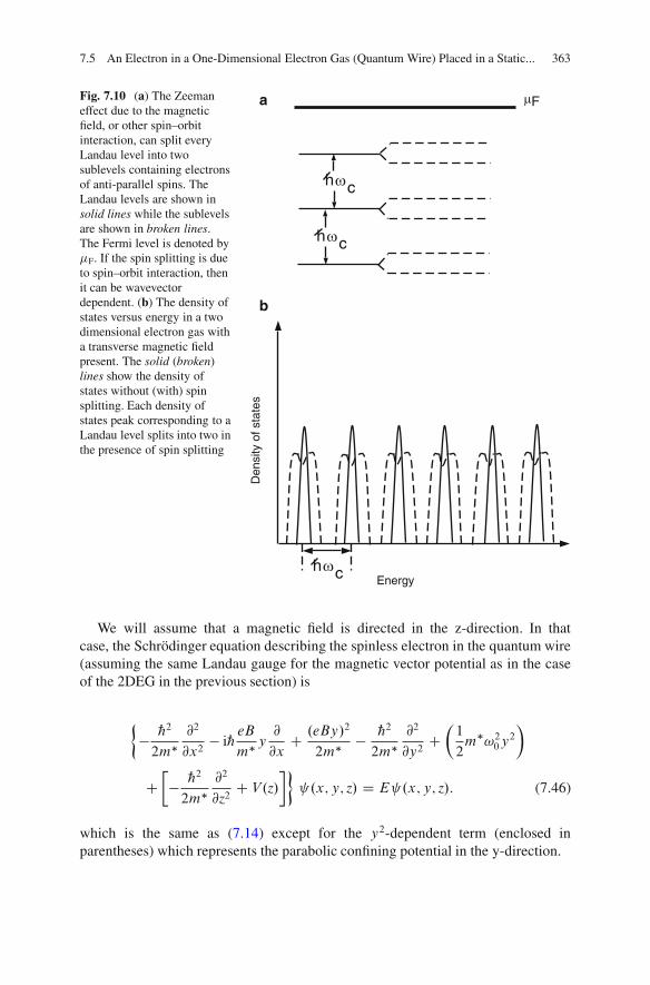
7.5 An Electron in a One-Dimensional Electron Gas (Quantum Wire) Placed in a Static... 363
hωc
hωc
hωc
Den
sity
of s
tate
s
Energy
a
b
μFFig. 7.10 (a) The Zeemaneffect due to the magneticfield, or other spin–orbitinteraction, can split everyLandau level into twosublevels containing electronsof anti-parallel spins. TheLandau levels are shown insolid lines while the sublevelsare shown in broken lines.The Fermi level is denoted by�F. If the spin splitting is dueto spin–orbit interaction, thenit can be wavevectordependent. (b) The density ofstates versus energy in a twodimensional electron gas witha transverse magnetic fieldpresent. The solid (broken)lines show the density ofstates without (with) spinsplitting. Each density ofstates peak corresponding to aLandau level splits into two inthe presence of spin splitting
We will assume that a magnetic field is directed in the z-direction. In thatcase, the Schrodinger equation describing the spinless electron in the quantum wire(assuming the same Landau gauge for the magnetic vector potential as in the caseof the 2DEG in the previous section) is
� „22m�
@2
@x2� i„ eB
m� y@
@xC .eBy/2
2m� � „22m�
@2
@y2C�1
2m�!20y2
�
C�
� „22m�
@2
@z2C V.z/
��
.x; y; z/ D E .x; y; z/: (7.46)
which is the same as (7.14) except for the y2-dependent term (enclosed inparentheses) which represents the parabolic confining potential in the y-direction.

364 7 Magnetic Field Effects in a Nanostructured Device
Split gates
Magnetic field
quantum wire
x
y
z
Fig. 7.11 A quantum wiredefined by a split gate on a2DEG. A magnetic field isdirected perpendicular to theplane of the 2DEG. Theconfining potential along they-direction is parabolic
Once again, since there are no mixed terms in the Hamiltonian involving morethan one coordinate, the wavefunction can be written in a product form as in (7.15).Moreover, since the Hamiltonian is invariant in the x-coordinate, the x-componentof the wavefunction is still given by (7.16). Substituting this wavefunction in (7.46),we get the equations
�„2k2x2m� C „kx eB
m� y C .eBy/2
2m� C 1
2m�!20y2 � „2
2m�@2
@y2
�
�.y/ D ��.y/
�� „22m�
@2
@z2C V.z/
�
�.z/ D �.z/; (7.47)
where E D �C . Here, we have once again decoupled the x-y motion from thez-motion, as we did before in the 2DEG case.
The first line of the preceding equation can be written as
�
� „22m�
@2
@y2C 1
2m�!2c .y C y0/
2 1
2m�!20y2
�
�.y/ D ��.y/; (7.48)
where the various quantities are defined by (7.22).

7.5 An Electron in a One-Dimensional Electron Gas (Quantum Wire) Placed in a Static... 365
Simplifying, we get"
� „22m�
@2
@y2C 1
2m�!2c!20
!2y20 C 1
2m�!2
�
y C !2c!2y0
�2#
�.y/ D ��.y/; (7.49)
where !2 D !20 C !2c .Transposing the constant term from the left-hand-side to the right-hand-side, we
obtain"
� „22m�
@2
@y2C 1
2m�!2
�
y C !2c!2y0
�2#
�.y/ D�
�� 1
2m�!2c!20
!2y20
�
�.y/:
(7.50)This equation is the familiar Schrodinger equation describing simple harmonic
motion centered at coordinate y D �!2c!2y0. The solutions of this equation yield the
wavefunction and energy eigenstate associated with y-component of the motion:
�.y/ D �m.y/ D�
ˇ
1=22mmŠ
�1=2
Hm
�
ˇ
�
y C !2c!2y0
��
e�.1=2/ˇ2
�
yC !2c!2y0
�2
� D �m D�
mC 1
2
�
„! C 1
2m�!2c!20
!2y20 ; (7.51)
where ˇ D p
m�!=„ ¤ p
m�!c=„. Therefore, ˇ ¤ ˛ D 1=rc. This then yieldsthe total energy and eigenstate as
E D Em;n D �m Cn D�
mC 1
2
�
„! C 1
2m�!2c!20
!2y20 C „2
2m�
�n
Wz
�2
D�
mC 1
2
�
„! C „2k2x2m�
�!!0
C „22m�
�n
Wz
�2
.x; y; z/ D �.x/�m.y/�n.z/ D 1pLx
eikxx
��
ˇ
1=22mmŠ
�1=2
Hm
�
ˇ
�
y C !2c!2y0
��
e�.1=2/ˇ2
�
yC !2c!2y0
�2
�s
2
Wzsin
�nz
Wz
�
; (7.52)
where obviouslyLx is the normalizing length in the x-direction andWz is the widthof the quantum well in the z-direction.
It is easy to see that these equations become identical to the correspondingequations for the two-dimensional case when !0 becomes zero, because then theconfinement in the y-direction vanishes and the quantum wire becomes a quantumwell.

366 7 Magnetic Field Effects in a Nanostructured Device
E
kx
E
kx
a b
Fig. 7.12 Dispersion relations in different hybrid magneto-electric subbands at (a) low magneticfields, and (b) high magnetic fields in a quantum wire with parabolic confinement potential in thedirection transverse to the magnetic field and the wire axis
In Fig. 7.12, we plot the energy dispersion relation E versus kx . Note thatwith increasing magnetic field, the energy spacing between the subbands increasesand the curvatures of the parabolas decrease, as if the effective mass defined as
„2=�@2E@k2x
increases. The effective mass in this case is�
1C .!c=!0/2�
m�, which
obviously increases with increasing magnetic field strength. Ultimately, in the limitof infinitely strong magnetic field, the curvatures reduce to zero, the effective massbecomes infinity, and the dispersion curves become totally flat and resemble the dis-persion curves of Landau levels in the 2-DEG shown in Fig. 7.2b. The reader shouldunderstand that this happens because in the presence of a very strong magnetic field,the cyclotron orbit diameters 2
pmrc D 2
p
m„= .m�!c/ (mD integer) becomemuch smaller than the effective width of the quantum wire which is 2
p„=.m�!0/.At that point, the electron goes around in cyclotron orbits without ever becomingquite aware of the confinement in the y-direction due to the electrostatic potentialV.y/. Since an electron in a cyclotron orbit has no translational velocity, its effectivemass is infinity. The magnetic field causes magnetostatic confinement by bindingthe electron into cyclotron orbits, while the parabolic confining potential causeselectrostatic confinement. When the magnetostatic confinement overwhelms theelectrostatic confinement (this happens when !c � !0, or when B � m�!0=e),the electron no longer feels the electrostatic confinement in the y-direction and thedifference between the one-dimensional case and the two-dimensional case getsblurred.
The states given by (7.51) are called hybrid magnetoelectric states since theyare a consequence of both magnetostatic confinement and electrostatic confinementin the y-direction. Note that in the 2-DEG , we had magnetostatic confinement inthe x-y plane (because the magnetic field is in the z-direction) and electrostatic

7.5 An Electron in a One-Dimensional Electron Gas (Quantum Wire) Placed in a Static... 367
confinement in the z-direction. Here, we have magnetostatic confinement in the x-yplane (once again because the magnetic field is in the z-direction) and electrostaticconfinements along both y- and z-directions. The y-component of motion thereforeexperiences both magnetostatic and electrostatic confinements.
Note also that the electrostatic confinement represented by the curvature !0and the magnetostatic confinement represented by the curvature !c add to createan effective magneto-electric confinement represented by the curvature !, where!2 D !20 C !2c .
Finally, note that the simple harmonic motion is now centered at �!2c!2y0. If the
electrostatic confinement is much stronger than the magnetostatic confinement, i.e.,!0 � !c (which happens at weak magnetic field strengths), then the center is at
ycenter D !2c!2y0 � !2c
!20y0
D 1
!20
�eB
m�
�2 „kxeB
D 1
!20
eB
m�„kxm� D e„kx
.m�!0/2B: (7.53)
Therefore, with increasing magnetic field, the center of simple harmonic motion,ycenter, gets pushed farther and farther away from the origin of the y-coordinate. Thatis, it gets pushed away from the axis of the wire toward the edges and the electronstend to localize at the edges of the quantum wire. This behavior is opposite to that ina 2DEG, where increasing magnetic field moved the center closer to the origin of they-axis. Unlike a quantum wire, a quantum well has infinite extent along the y-axisand hence no “edges.” Note two important features: (1) electrons with oppositesigns of the wavevectors (and hence possibly opposite velocities) get pushed towardopposite edges. We expect that from the classical picture because the Lorentz forceeEv � EB acts in opposite directions on oppositely traveling electrons; (2) electronsand holes with the same kx get pushed toward opposite edges in a quantum wiresince their charges have opposite signs e and �e. This is the basis of the QCLEthat we will discuss later. The traditional Hall effect has a different basis. There,an electric field is applied along the length of the wire so that electrons and holesdrift in opposite directions and have opposite signs of kx . Therefore, their oppositecharges actually push them toward the same edge.3 This will tend to prevent buildingup of the Hall voltage and indeed the Hall effect is weak in bipolar materials thathave nearly equal concentrations of electrons and holes. Only if the concentrationsof electrons and holes are vastly different (as in a unipolar material that is eithern-type or p-type), will a significant Hall voltage develop between the two edges andgive rise to the Hall effect.
3Classically, the Lorentz force qEv � EB [q = particle charge] on the electron and hole have the samedirection since both Ev and q are opposite for the two particles. Therefore, both particles are pushedin the same direction.

368 7 Magnetic Field Effects in a Nanostructured Device
7.5.2 Quantum Wire with Rectangular ConfinementPotential Along the Width
So far, we have considered a quantum wire with parabolic confining potential in they-direction (direction mutually perpendicular to both the wire axis and the magneticfield). Let us now consider a quantum wire with rectangular cross-section wherethe confining potentials along both width (y-direction) and thickness (z-direction)are rectangular with infinite barriers. A magnetic field is applied in the z-direction.We are interested in finding the wavefunctions and energy dispersion relations ofthe hybrid magneto-electric states in this case, for which we need to solve the time-independent Schrodinger equation. Unfortunately, the Schrodinger equation doesnot have an analytical solution in this case and must be solved numerically, asdescribed below.
The effective mass time-independent Schrodinger equation will be
8
<
:
h
�i„ Err � e EA.x; y; z/i2
2m� C V.y/C V.z/
9
>=
>;
.x; y; z/ D E .x; y; z/; (7.54)
where the confining potentials are:
V.y/ D 0 .jyj � Wy=2/
D 1 .jyj > Wy=2/
V.z/ D 0 .jzj � Wz=2/
D 1 .jzj > Wz=2/; (7.55)
with Wz being the thickness andWy the width.The magnetic field is directed along the z-direction and the associated flux
density isB Oz. Choosing the Landau gauge, we write the magnetic vector potential as
EA.x; y; z/ D �By Ox: (7.56)
Since there are no mixed terms in the Hamiltonian, we can write the wavefunc-tion in a product form:
.x; y; z/ D '.x/�.y/�.z/: (7.57)
Furthermore, because the Hamiltonian is invariant in x, the x-component of thewavefunction is a plane wave given by
'.x/ D 1pLx
eikxx: (7.58)

7.5 An Electron in a One-Dimensional Electron Gas (Quantum Wire) Placed in a Static... 369
The reader can easily verify that we can now write the Schrodinger equation astwo equations after decoupling the z-component of motion:
@2�.y/
@y2C 2m�
„2 �1�.y/��y
r2c
�
�.y/C 2y
r2ckx�.y/ � k2x�.y/ D 0
@2�.z/
@z2C 2m�
„2 �2�.z/ D 0: (7.59)
where rc is the cyclotron radius given by rc D p„=.eB/, and E D �1 C �2.The solution of the second subequation in the preceding equation (subject to the
boundary conditions in (7.55)) are particle-in-a-box states�.z/ D .2=Wz/
1=2 sin.nz=Wz/. The solution of the first subequation is morechallenging. We would like to solve it as an eigenvalue problem (subject to theboundary conditions in (7.55)) where we find the values of the wavevector kx fora given value of �1 and repeat this procedure for different �1 to find the energydispersion relation (�1 versus kx) of the hybrid magneto-electric states. At the sametime, the eigenvectors will give us the wavefunctions �.y/ of the hybrid magneto-electric states. Unfortunately, this is not straightforward since the first subequation isnot an eigenequation in kx for a given �1 because it is not linear in kx . We thereforeuse the following transformation:
Let
�.y/ D kx�.y/: (7.60)
We can then write the nonlinear equation as two coupled linear equations:
"0 1
@2
@y2C 2m�
„2 �1 ��y
r2c
22y
r2c
#��.y/
�.y/
�
D kx
��.y/
�.y/
�
: (7.61)
The last equation was solved numerically in [12], subject to the boundarycondition in (7.55), using a finite difference scheme. The y-domain was discretizedinto N grid points, resulting in a 2N � 2N matrix which has 2N different kxeigenvalues (kŒ1�x ;˙kŒ2�x ; : : : ˙ k
Œ2N �x ) for any given energy �1, with corresponding
eigenvectors that give the wavefunction �n.y/. A pair of kŒn�x values will correspondto a magneto-electric subband (the two members of the pair yield the positive andnegative wavevectors at energy �1 in the corresponding subband). In this process,one obtains as many subbands as the number of grid points N . Some of the kŒn�xvalues will turn out to be imaginary or complex, and the others will be real. Thesubbands with real kx have their minimum energy (subband bottom) below �1 andconstitute propagating states, while subbands with nonreal kx have their minimumenergies (subband bottom) above �1 and are evanescent. The dispersion relationsfor different (propagating) magneto-electric subbands are shown schematically inFig. 7.13. These dispersion relations are plotted as �1 versus kx C .eB=„/y0, where

370 7 Magnetic Field Effects in a Nanostructured Device
ε1 ε1
kx + (eB/h)y0
a b
kx + (eB/h)y0
Fig. 7.13 Dispersion relations in different magneto-electric subbands in a quantum wire withrectangular confining potential at (a) low magnetic fields, and (b) high magnetic fields in a quantumwire with rectangular confining potential in the direction transverse to the magnetic field and thewire axis. Only the dispersion relations of propagating states are shown
y0 D h�n;k0.y/jyj�n;k0.y/i. The quantity k0 is the wavevector at which the bottomof the magneto-electric subband occurs, i.e., where @�1=@kx D 0. Note that y0is different in different magneto-electric subbands because �n;k0.y/ is different.The reason we plot the dispersion relations as �1 versus kx C .eB=„/y0, insteadof as �1 versus kx , is because then the curves are symmetric about the energy axis.Otherwise, if we plotted them as �1 versus kx , then each curve will be displacedhorizontally from the energy axis by an amount �.eB=„/y0, which would bedifferent in different subbands since y0 is subband dependent. It is important tounderstand that in a magnetic field, the electron’s velocity vx ¤ „kx=m�, even ifthe bandstructure is parabolic, but vx D .1=„/@�1=@kx .
7.5.2.1 Edge States
The dispersion relation in Fig. 7.13 can also be viewed as a plot of energy versus they-coordinate, where kx D 0 corresponds to the center of the quantum wire (yD 0).We state this here without explicit proof because it gives us some insight into whythe dispersion relations are so different at high and low magnetic fields. At highfields, the lowest subband dispersion relations have “flat” bottoms and the velocityof an electron vx D .1=„/@E=@kx is zero there. Since the bottoms straggle kx D 0
(or, equivalently, y D 0), this means that an electron’s velocity is zero at or aroundthe wire’s axis. We expect that to happen at high fields when the cyclotron radiuspmrc D p
m„=.eB/ Wy=2 (mD the subband index or the Landau level index)for the lowest subbands. In that case, an electron at or near the wire’s axis, in thelowest subbands (which have the smallest cyclotron radii), can complete a cyclotronorbit without ever hitting the walls of the wire located at y D ˙Wy=2. Since the

7.5 An Electron in a One-Dimensional Electron Gas (Quantum Wire) Placed in a Static... 371
expectation value of the velocity operator of an electron in a cyclotron orbit is zero(see (7.26)), the dispersion relations of the lowest subbands should have flat bottoms(i.e., .1=„/@�1=@kx D 0) around kx D 0, which indeed they do. On the other hand,at low magnetic fields, rc > Wy=2 and an electron cannot complete a cyclotronorbit without hitting the walls, even if it is in the lowest subband with mD 1.Since the electron cannot complete a closed cyclotron orbit, it will never have zerotranslational velocity in the x-direction. Consequently, the dispersion relations atlow magnetic fields will not have flat bottoms. Actually, even at high magnetic fields,the higher subbands do not have flat bottoms because they have larger cyclotronradii equal to
pmrc (m � 1) which do not fulfill the requirement
pmrc < Wy=2.
An electron in the higher subbands therefore cannot execute cyclotron motion andhave zero translational velocity even at relatively high magnetic fields. As a result,the higher subbands do not have flat bottoms.
Note also that at high magnetic fields, only states with large kx values in thelowest subbands have nonzero slopes in the dispersion relations and therefore havenonzero velocities. That means only electrons that are far from the center of thewire, or are close to either edge of the wire, have nonzero translational velocityand can carry current. These states are justifiably called edge states because theyhug the edges of the wire, and are the only states that can carry current in a highmagnetic field. Note also that the slope of the dispersion relation is positive at oneedge and negative at the other edge. Hence, edge states localized at opposite edgescarry current in opposite directions. This is not unlike the parabolic confinementcase where electrons localized at opposite edges carry current in opposite directions.
In Fig. 7.14, we show schematically the wavefunctions �C.y/ and ��.y/ inthe lowest magneto-electric subband for two states at the same energy but withoppositely directed wavevectors ˙kx . The value of kx was chosen such that themagnitude of the slope of the dispersion curve at that wavevector is large. Note thatat low magnetic fields, the two wavefunctions are only slightly displaced from eachother in the y-direction and still have a significant overlap (the mutual displacementwould have been zero at zero magnetic field), but at high magnetic fields, theyare very much displaced from each other and have virtually no overlap. In fact,the wavefunction for positive velocity is localized along the left edge of the wire,while that for negative velocity is localized at the right edge. These are edge statewavefunctions. Therefore, at high magnetic fields, all current carrying states, thathave large translational velocities (i.e., large slopes in the dispersion curves), arelocalized at one edge or the other.
In Fig. 7.15b, we show the electron trajectories in a quantum wire at highmagnetic field. The trajectories at the center are closed cyclotron orbits, while thoseat the edges are incomplete orbits that hit the walls, rebound, and loop around toform what are known as “skipping orbits.” The latter obviously travel along the wire,while hugging the walls, and have nonzero effective velocities. The skipping orbitsmake up the edge states. Note that skipping orbits at opposite edges are skippingalong in opposite directions and hence carry current in opposite directions.

372 7 Magnetic Field Effects in a Nanostructured Device
Magnetic field
Magnetic field
x
y
z
φ (y)-
φ (y)-
φ (y)+
φ (y)+
Current in
Current in
Current out
Current out
a
b
Fig. 7.14 The wavefunctions �C.y/ and ��.y/ in the lowest magneto-electric subband for twostates at the same energy but with oppositely directed wavevectors ˙kx : (a) low magnetic fields,and (b) high magnetic fields. The wavevector kx is chosen such that the slope of the dispersionrelation of the lowest magneto-electric subband at that wavevector is relatively large. At highmagnetic fields, the wavefunctions are those of edge states

7.5 An Electron in a One-Dimensional Electron Gas (Quantum Wire) Placed in a Static... 373
x
z
y
Magnetic field
a
b
Skipping orbits
Closed cyclotronorbit
Fig. 7.15 Electron trajectories in real space in a quantum wire: (a) low magnetic field, and (b)highmagnetic field where cyclotron orbits form at the center and skipping orbits result at the edges
7.5.3 Edge State Phenomena
Edge states give rise to many intriguing phenomena, but one that we can predictalmost immediately is suppression of backscattering in a quantum wire. In aquantum wire, an electron can either travel forward along the wire, or backwardsince sideways motion is restricted by the walls of the wire. A forward travelingelectron can be scattered forward with little change in momentum, or scatteredbackward with a large change in momentum. The backscattering event will causelarge momentum relaxation and degrade mobility rapidly, while forward scatteringwill have little effect on mobility since it does not cause much momentumrelaxation.

374 7 Magnetic Field Effects in a Nanostructured Device
In a strong magnetic field, backscattering will need to transfer an electronfrom one edge of the quantum wire to the other since electrons traveling inopposite directions are localized at opposite edges. However, the spatial overlapbetween the two edge state wavefunctions is very small as can be seen fromFig. 7.14b. Consequently, the matrix element for backscattering (recall that forphonon scattering, the matrix element is proportional to the square of the overlapbetween the initial and final state wavefunctions) is very small as well. Hence,in accordance with Fermi’s Golden Rule, the rate of backscattering S.k; k0/ isvery small. This has two immediate consequences: (1) the carrier mobility shouldincrease in a magnetic field because backscattering will be severely suppressed, and(2) the probability that an electron entering at one end of the wire will exit at theother end is very high. That means that the transmission probability through thewire is high and reflection probability is low. The latter has an important role toplay in the integer quantum Hall effect that we will discuss later in this chapter.The quenching of backscattering in a magnetic field can be quite significant andthe energy-averaged scattering rate may go down by several orders of magnitude atreasonable magnetic field strengths [13].
Finally, an important question that should arise is whether edge states andcyclotron orbit states will always form in a quantum wire. Before we answer thisquestion, we should compare the high-field dispersion relations in Figs. 7.12b and7.13b, which are for parabolic confining potential and rectangular confining poten-tial, respectively. There is an obvious difference between them. In the parabolic case,there are no states with zero velocity since no dispersion curve has a flat bottom.Every state carries current at any finite magnetic field. In the rectangular case, thereis a clear demarcation between states in the center of the wire that form closedcyclotron orbits and have no translational velocity (thereby carrying no current),and edge states localized at the two edges that form skipping orbits and carry currentin opposite directions. The reason that cyclotron orbits isolated from the walls donot form in a parabolic confining potential is that the confining potential variescontinuously along the y-direction so that there is no region of constant potentialwhere a closed cyclotron orbit can be located and carry no current. Also note thata parabolic confining potential has no “edge” and therefore it makes no sense totalk about edge states in a parabolic potential. That is why the demarcation betweenedge states and cyclotron orbit states is lost in the parabolic case.
7.5.4 Shubnikov–deHaas Oscillations in a QuasiOne-Dimensional Electron Gas
We saw earlier that the conductance of a 2DEG oscillates in a magnetic fieldand is periodic in 1=B where B is the flux density. These are Shubnikov–deHaasoscillations. An interesting question is whether the same oscillations can occur in a1DEG. We know that in order for these oscillations to be manifested, the electrons

7.6 The Quantum-Confined Lorentz Effect 375
must be able to complete cyclotron orbits and that can happen only if the diameter ofthe smallest orbit 2rc is smaller than the effective width of the quantum wire, whichis 2
p„=.m�!0/ in the case of parabolic confining potential. Therefore, Shubnikov–deHaas oscillations will appear when the magnetic flux density B > 1=� andB > m�!0=e, or !c > !0. In the case of rectangular confining potential, theseoscillations will appear when B > 1=� and rc D p„=.eB/ < Wy=2, i.e.,when B > 2.h=e/.1=W 2
y /. However, the interplay between the electrostaticconfinement and magnetostatic confinement can cause complicated features inthe magnetoresistance oscillations that are not seen in normal Shubnikov–deHaasoscillations [14].
7.6 The Quantum-Confined Lorentz Effect
Consider a quantum wire with parabolic confining potential along its width(y-direction in Fig. 7.14). A weak magnetic field of flux density B is applied in thez-direction. The centers of the hybrid magneto-electric wavefunctions for electronsand holes are obtained from (7.53):
yelectroncenter D jej„ke
xB�
me!e0
2
yholecenter D � jej„kh
xB�
mh!h0
2; (7.62)
where kex is the wavevector of the electron along the wire’s length, kh
x is thewavevector of the hole,me is the electron’s effective mass,mh is the hole’s effectivemass, !e
0 is the curvature of the confining potential for electrons, and !h0 is that
for holes. Note that we have accounted for the fact that electrons and holes haveopposite charges and hence there is a minus sign preceding the right-hand side ofthe second line in the last equation.
It is now obvious that the magnetic field pushes the center of the hole’swavefunction and that of the electron’s wavefunction in opposite directions fromthe wire’s axis as long as ke
x and khx have the same sign (because then yelectron
center andyhole
center will have opposite signs). In the case of optical absorption, kex D kh
x byvirtue of the celebrated k-selection rule that we discussed in Chap. 6. Therefore, theelectron and hole coupled by a photon in the optical absorption process will havetheir wavefunctions skewed in opposite directions by the magnetic field as shownin Fig. 7.16. Insofar as the strength of absorption (for light polarized along the wireaxis) is proportional to the square of the overlap between the electron and holewavefunctions (recall Chap. 6 material), this strength will decrease in a magneticfield because the overlap will be reduced. Therefore, the magnetic field will quenchoptical absorption, much like the electric field did in Quantum-Confined Stark Effectthat was discussed in Chap. 3.

376 7 Magnetic Field Effects in a Nanostructured Device
Potential energy Potential energy
Distance along width Distance along width
B = 0 B = 0
φe φe
φh φh
Abs
orpt
ion
Photon frequency
Ec
Ev
Ec
Ev
Abs
orpt
ion
Photon frequency
Fig. 7.16 Quantum-Confined Lorentz Effect. In a quantum wire (shown with parabolic confiningpotential along the width), a magnetic field will skew the electron and hole wavefunctions oftwo states with the same wavevector in opposite directions. This will reduce the overlap betweenthe wavefunctions and quench absorption. The electron and hole wavefunctions are shown withbroken lines. From the spread of the wavefunctions shown and assuming that the curvatures ofthe conduction and the valence bands due to parabolic confinement are the same, can you tellwhether the electron or the hole has the lighter effective mass in this case? In the bottom panel,the absorption spectra are shown in the absence (left) and presence (right) of a magnetic field.Note that the magnetic field quenches absorption and induces a blue shift in the absorption peak.The different absorption peaks are due to transitions between different electron and hole subbands.The emission spectrum (or photoluminescence spectrum) will exhibit similar behavior
We call this magnetic field induced effect QCLE [15] because its classical analogis related to the Lorentz force. The Lorentz force qEv � EB on an electron and a holemoving in the same direction will be oppositely directed because the particles haveopposite charges. Hence, a magnetic field will force them apart. Now, two particlesthat participate in absorption are always moving in the same direction by virtueof the k-selection rule. Hence, a magnetic field will push them away from eachother, which reduces the overlap between their wavefunctions and consequentlythe absorption strength. Note that this is very different from the Hall effect whereelectrons and holes are drifting under an applied electric field and therefore movingin opposite directions. Consequently, the Lorentz forces on them act in the same

7.7 The Hall Effect in a Two-Dimensional Electron Gas 377
direction and pushes them in the same direction. However, in the case of opticalabsorption, the particles must be moving in the same direction by virtue of the k-selection rule, so that the Lorentz force on them acts in opposite directions and keepsthem apart.
Although both QCLE and Quantum-Confined Stark Effect quench opticalabsorption, there are some obvious differences between them. First, the former isinduced by a magnetic field which always increases the energy separation between
electron and hole subbands since !0 !q
!20 C !2c . Therefore, the quenchingof absorption is always accompanied by a blue shift in the absorption spectrum.In the case of the Quantum-Confined Stark Effect, the quenching is typicallyaccompanied by a red shift. Second, the electric field used in Quantum-ConfinedStark Effect tends to make the confining potential shallower since it tilts the bands,which will ultimately allow the electron and hole to escape from the confiningpotential. In contrast, the magnetic field in QCLE makes the confining potential
stronger since !0 !q
!20 C !2c , which means that the curvature of the confiningpotential increases. These differences determine which would be preferred in opticalmodulation applications under a given set of conditions.
7.7 The Hall Effect in a Two-Dimensional Electron Gas
Consider an ideal two-dimensional electron gas (2-DEG) in the x-y plane as shownin Fig. 7.1. A magnetic field is applied perpendicular to the plane in the z-direction.Now, if a current flows in the x-direction, then a Lorentz force will appear on theelectrons which will be directed in the y-direction. This will cause the electrons tobe deflected in the y-direction and a charge imbalance will result which will giverise to a Hall electric field (see Fig. 1.3). The force due to this field will eventuallybalance the Lorentz force and steady state will be reached. If we call the steady-stateHall field EHall
y , then
EHally D vxBz; (7.63)
where vx is the x-directed velocity of the electron andBz is the magnetic flux density(in the z-direction).
Integrating the last equation over the y-coordinate, we obtain:
VHall D Vy DZ W
0
EHally dy D vxBz
Z W
0
dy D vxBzW; (7.64)
whereW is the width of the 2-DEG and VHall is the Hall voltage that is generated.The current density in the 2-DEG is given by
Jx D nevx; (7.65)

378 7 Magnetic Field Effects in a Nanostructured Device
where n is the electron concentration. The resulting current flowing in the x-direction is
Ix D W tJx D ntWevx D nsWevx; (7.66)
where ns D nt is the sheet electron concentration. This yields that vx DIx=.Wens/.
Substituting the last result in (7.64), we get
VHall
IxD Vy
IxD Bz
ens: (7.67)
Normally, because of the Hall electric field in the y-direction, a current couldflow in that direction as well. Therefore, we can write:
�VxVy
�
D�Rxx RxyRyx Ryy
� �IxIy
�
; (7.68)
where the square matrix is the resistance tensor. The diagonal term Rxx is calledthe “longitudinal resistance” and the off-diagonal term Ryx is called the “Hallresistance.”
If we were carrying out a Hall experiment to measure the Hall resistance, wewould have connected a voltmeter across the sample’s width to measure the Hallvoltage VHall D Vy . Since an ideal voltmeter would have had infinite impedance, nocurrent would have flowed in the y-direction and consequently, Iy D 0: Therefore,(7.68) would have yielded the Hall resistance as
RHall D Ryx D Vy
IxD VHall
IxD Bz
ens: (7.69)
Consider the situation when the electrons are not spin polarized. Since (see(7.35)) ns D p=.2eBz=h/, where p is the number of fully filled Landau levels(sometimes called the “filling factor”), we immediately get that ideally the Hallresistance should be quantized and given by
RHall D Ryx D 1
p
h
2e2D 1
p
1
4˛f c�0; (7.70)
where c is the speed of light in vacuum, �0 is the dielectric constant of vacuum,and ˛f is a dimensionless constant known as the “fine-structure constant,” with avalue of 1/137 D 0.00729720. This is a remarkable result since it predicts that theHall resistance will not depend on the electron concentration in the sample and, infact, will be independent of all sample parameters! It will depend only on universalconstants h and e.
At very high magnetic fields, the electrons may be fully spin polarized and thiswill remove the spin degeneracy, which means that each spin-degenerate level splits

7.7 The Hall Effect in a Two-Dimensional Electron Gas 379
into two distinct levels at different energies. Consequently, for the same carrierconcentration ns , the number of fully filled Landau levels will be p0 D 2p (see(7.35) and (7.36)). In that case, the last equation will become
RHall D Ryx D 1
p0h
e2D 1
p
h
2e2; (7.71)
which is the same result as before, since ns has not changed. Therefore, the Hallresistance is quantized in units of h=e2, which is 25.56 k-ohms.
The last equation predicts that if we measure the Hall resistance of an ideal spin-polarized two-dimensional electron gas (2-DEG) while progressively decreasing p0by successive depopulation of spin-nondegenerate Landau levels with an increasingmagnetic field, then we should observe the Hall resistance increase in steps, withthe last step having a height of h=e2, or 25.56 k˝ corresponding to p0 D 1. Thiswill happen as long as the magnetic field is strong enough to cause complete spinpolarization of all the electrons. The steps occur because the quantity p0 is aninteger, so that every time a spin-nondegenerate Landau level is depopulated, theHall resistance jumps by precisely 1
p0.p0C1/he2
. The quantity p0 is referred to as the“filling factor” since it is the number of Landau levels filled with electrons. Fromthe height of any resistance step, one can infer the corresponding filling factor.
In an actual experiment, we could progressively decrease p0 in two ways: (1)We could hold the Fermi level in the 2-DEG invariant by holding the sheet carrierconcentration ns constant and vary the magnetic field strength which increases theseparation between successive Landau levels (as well as the spin splitting withineach level) since the separation is „!c D „.eB=m�/. This would decrease p0with increasing magnetic field strength, as is obvious from (7.36). Alternately, (2)we could hold the magnetic field constant so that the energy separation betweensuccessive Landau levels and the spin splitting do not change, but we vary theposition of the Fermi level (with respect to the Landau levels) by varying thesheet carrier concentration ns . This too would change p0 in accordance with (7.36)(Fig. 7.17).
In the year 1980, a group of experimentalists reported measuring the Hall resis-tance of a 2-DEG formed in the inversion layer of a metal-oxide-semiconductor-field-effect-transistor as a function of the sheet carrier concentration ns [16]. Thelatter quantity was varied using the voltage applied to the gate terminal of thetransistor. These measurements were carried out at low temperature (liquid helium)and very high magnetic field strengths (�15 Tesla) so that the electrons werenearly fully spin polarized. It was found that the Hall resistance indeed decreasedin steps as p0 was increased by increasing ns with the gate voltage. The heightof each step was precisely .1=n/h=e2 [nDp0.p0 C 1/D an integer] as predictedby (7.71) and it did not depend on any sample parameter. In fact the step heightagreed with the value .1=n/h=e2 with surprising precision (1 part in 105). Theexperimental plot of the Hall resistance versus the gate voltage is shown in Fig. 7.18.Another intriguing observation was that whenever the Hall resistance Ryx was in aplateau, the longitudinal resistance Rxx reached zero. This phenomenon came to be

380 7 Magnetic Field Effects in a Nanostructured Device
I
V
VHall
x
y
z
Wt
Increasing sheet carrier concentration ns
Ryx
[1/(n+1)](h/e2) [1/n](h/e2)
Rxx Magnetic field held constant
Res
ista
nce
Rxx
R yx
Increasing magnetic field
Res
ista
nce
Carrier concentration held constant
Ryx
classical
a
b
c
Fig. 7.17 (a) Schematic of a Hall bar sample for measuring Hall resistance and longitudinalresistance. (b) The quantized Hall resistance Ryx D VHall=I (solid line) and the longitudinalresistance Rxx D V=I (broken line) as a function of the sheet carrier concentration in a 2-DEGwhen the magnetic flux density B is held constant at a high value. (c) The same quantities as afunction of the magnetic flux density B when the sheet carrier concentration ns is held constant.The dotted line shows the classical Hall resistance which increases linearly with the magnetic fluxdensity. This line often intersects the quantum Hall plateaus at the mid-points. In order to observesuch quantized Hall resistance, the temperature must be kept low and the voltage V must be lowas well. These plots are highly idealized for illustrative purposes

7.7 The Hall Effect in a Two-Dimensional Electron Gas 381
Fig. 7.18 The Hall voltage UH (or, equivalently, the Hall resistance Ryx) and the voltage betweenvoltage probes Upp (or, equivalently, the longitudinal resistance Rxx) as a function of the gatevoltage in the inversion layer of a MOSFET at a temperature of 1.5 K with a constant magnetic fieldof 18 Tesla directed perpendicular to the layer. The inset shows the schematic of the experimentalstructure. The distance between current probes is 400�m, the distance between voltage probesis 130�m and the width is 50�m. Reproduced from [16] with permission from the AmericanPhysical Society. Copyright American Physical Society 1980. See http://prl.aps.org/abstract/PRL/v44/ i6/p494 1
known as the celebrated integer quantum Hall effect. Since then, the quantum Hallresistance—which always agrees so precisely with the value .1=n/h=e2—has beenproposed as a metrological standard of resistance. To date, this resistance has beenmeasured with an accuracy of few parts per billion and always agrees with the value.1=n/.h=e2/ [17].

382 7 Magnetic Field Effects in a Nanostructured Device
7.8 The Integer Quantum Hall Effect
It may appear that the effect observed is fully explained by the theory just discussed,but that is deceptive. The theory discussed applies only to an ideal 2-DEG with noimpurity and no other imperfection. That does not conform to the disordered channelof a metal-oxide-semiconductor-field-effect-transistor, which will be replete withimpurities and imperfections. Moreover, the theory does not explain why the effectis observed only at low temperatures and high magnetic fields. Most importantly, itdoes not explain why the longitudinal resistance Rxx will vanish whenever the Hallresistance is in a plateau. Therefore, a much more profound theory is called for toexplain all these observations. That theory was first postulated by Laughlin [18],who invoked principles of gauge invariance and showed that the Hall resistanceshould be quantized even in a nonideal 2-DEG. He discussed the response of acylindrical sample to a magnetic field directed along the axis of the cylinder andexplained the emergence of the quantized Hall resistance as a consequence of asupercurrent caused by the phase rigidity of the long range wavefunction around thesample’s circumference and gauge invariance. This argument, however, can onlyapply to cylindrical conductors whose circumference is so short that an electrontraveling around the circumference will never encounter any phase randomizingcollision event so that its phase will remain conserved. Real samples that exhibitthe integer quantum Hall effect are, however, neither cylindrical nor shorter thanthe phase coherence length of electrons. Consequently, the phase rigidity of thewavefunction is never realized. Moreover, a cylindrical sample is a closed conductorwith no leads while the integer quantum Hall effect is measured in open conductorswith leads that allow electrons to enter and exit the device. Therefore, Laughlin’stheory, albeit elegant, is not a completely satisfactory explanation of the integerquantum Hall effect. Later, an alternate theory was advanced by Buttiker [19] thatdid not require phase rigidity of the wavefunction, or the other assumptions. We willdiscuss it in Chap. 9.
7.9 The Fractional Quantum Hall Effect
In 1982, another group of experimentalists reported observing quantized Hallplateaus, but with a different twist. They found that at very high magnetic fieldsand low temperatures, the Hall resistance in their 2-DEG samples were quantized tothe value
RHall D 1
l
h
e2D 1
l
1
2˛f c�0; (7.72)
where the quantity l was a fraction (l D 1=3) [20]. This was called the fractionalquantum Hall effect. Since then, many other “fractions” have been discoveredcorresponding to

7.9 The Fractional Quantum Hall Effect 383
Fig. 7.19 The longitudinal (�xx ) and Hall (�xy ) resistances of a two dimensional electron gas asa function of magnetic field at a temperature of 150 mK. Reproduced from [22] with permissionof the American Physical Society. Copyright American Physical Society 1987. See http://prl.aps.org/abstract/PRL/v59/ i15/p1776 1
l D m
2mC 1D 1
3;2
5;3
7;4
9; : : : : :
l D m
4mC 1D 1
5;2
9;3
13; : : : : :
l D 1 � m
2mC 1D 2
3;3
5;4
7;5
9: : : : :
l D 1 � m
4mC 1D 4
5;7
9;10
13; : : : : : (7.73)
Additionally, the fractions 2/7, 3/11, and 4/15 have also been observed. Allobserved fractions have an odd denominator [21], with the sole exception of afraction 5/2 [22] where it was later found that the 2-DEG was not completely spinpolarized [23]. Figure 7.19 shows the longitudinal and Hall resistances as a functionof magnetic field in a 2-DEG, reported in [22].

384 7 Magnetic Field Effects in a Nanostructured Device
The FQHE is a many-body effect that cannot be explained without accounting forthe interaction between the numerous electrons in a 2-DEG. The wavefunction givenin (7.25) is that of a single isolated electron, which does not take this interaction intoaccount. If we do take it into account then we must come up with a multi-electronwavefunction that describes all the interacting electrons in a sample.
The multi-electron wavefunction in the ground state of a 2-DEG subjected to astrong transverse magnetic field was postulated by Laughlin [24] as
n.x; y/ D ˘j<k.�j � �k/n exp
�14
X
q
ˇˇ�qˇˇ2
!
; (7.74)
where ˘ denotes multiplication, � D x C iy, and �q is the coordinate of the q-thelectron in the 2-DEG. The quantity n is an odd integer. Laughlin also showedthat the probability density associated with this multi-electron wavefunction canbe written as [24]
j n.x; y/j2 D e�ˇ�; (7.75)
where� is a dimensionless potential given by
� D �X
j<k
2n2 ln j�j � �kj C 1
2nX
q
jzq j2: (7.76)
and ˇ D 1=n.The all-important question now is what will be the quantum Hall resistance of
a 2-DEG described by the above multi-electron wavefunction? Before we proceedwith this question, we need to understand first the concept of a “quasi-particle,”since it will be vital in answering this question. In order to comprehend what aquasi-particle is, consider the fact that in a real solid there are numerous mobileelectrons moving around against a background of fixed positive charges due to theimmobile ions. The ionic charges balance those of the electrons to make the entiresolid charge-neutral. But now, because the positive background charges mildlyattract the mobile electrons, the electrons are really not all that free and mobile,but instead behave collectively like a viscous fluid (or “jelly”). Hence, the electronsea is sometimes called a “jellium.”
Next, we need to understand that the electrons in a jellium are not oblivious ofeach other. They mutually interact via Coulomb interaction so that their motionsare not independent, but correlated. Therefore, when an extra electron is introducedinto jellium, all other electrons will tend to move away from the intruder because ofCoulomb repulsion. This will expose a region around the intruder that is positivelycharged because of the background ions (see Fig. 7.20). The positively chargedannulus gets permanently attached to the intruding electron and moves with itwherever it goes [25]. Thus, the electron is “dressed” with a positively charged cloudwhich screens its negative charge partially. This composite entity (the electron withits surrounding positively charged cloud) is a quasi-particle, or quasi-electron, and

7.9 The Fractional Quantum Hall Effect 385
Electron sea
Intruder electron
Positivelycharged annulus
Fig. 7.20 An electron introduced into jellium pushes away the neighboring electrons owingto Coulomb repulsion, exposing an annulus of positive charges surrounding it. The positivecharges are due to the background positive ions in jellium. This positively charged annulus getspermanently attached to the electron and moves with it, partially screening its charge. The electronand its surrounding annulus constitute a “quasi-particle” whose effective charge is obviouslysmaller (less negative) than the bare electron’s charge. Adapted with permission from [25]
obviously its charge is less than that of the bare electron because of the screeningeffect of the annulus (the electron’s “dress”). It should be obvious now that wheneverwe are dealing with many interacting electrons, we really should not think in termsof bare electrons (which ignores the interaction with all other electrons), but insteadthink in terms of quasi-electrons.
Not only does the charged annulus dress a bare electron, but there are othereffects that can contribute to the dressing as well. For example, the background ionsare not completely immobile. At a finite temperature, they are vibrating in unisonand a quantum of this collective excitation is a phonon. When an electron passesthrough the vibrating lattice, the ions in its path are slightly attracted to the passingelectron because of Coulomb attraction. This responsive motion of the ions can bethought of as a phonon mode and we can think of this phonon dressing the electronas well. We had alluded to phonon dressing in Chap. 5. This will obviously makethe effective mass of the quasi-electron heavier because of the drag the ions exert.Thus, it is not only the other electrons, but the background ions could also dress anelectron. Such dressing is the cornerstone of Cooper pairing of electrons that leadsto superconductivity, but unfortunately we cannot delve further into this subject heresince it is beyond the scope of this book.
Laughlin showed that in a high magnetic field, the many-body ground stateof a two-dimensional sea of interacting electrons, described by the wavefunctionin (7.74), behaves like an incompressible quantum fluid. The quasi-electrons inthis fluid carry fractional charge of 1=n each, where n is an odd integer. He then

386 7 Magnetic Field Effects in a Nanostructured Device
proceeded to show that the quantum Hall resistance of such a fluid should beRHall D h
e�e, where e� D .1=n/e is the charge of the quasi-electron. Accordingly,
RHall D nhe2
D 1lhe2
, where l D 1=n. This could explain the experimental observationof the l D 1=3 effect since n is always odd.
Note that Laughlin’s theory does not explain the FQHE as the integer quantumHall effect of fractionally charged quasi-electrons since then we would simplyreplace e with e� and the Hall resistance would have been RHall D h
.e�/2D
n2he2
D 1l2
he2
, instead of nhe2
or 1lhe2
. Actually, it would have been very satisfyingto show that the FQHE is indeed nothing but the integer quantum Hall effect ofsome appropriate quasi-particles (different from Laughlin’s quasi-particles). Thatobjective was attained by Jain [26] who invoked the notion of “composite fermions”and showed that the FQHE is nothing but the integer quantum Hall effect of thesecomposite fermions. So, what are composite fermions?
Jain argued that at very high magnetic fields, the degeneracy of each occupiedLandau level will be very large because the degeneracy is given by (7.32) and itincreases with magnetic field strength. Since the degeneracy is the number of k-states in each Landau level and each k-state is occupied by an electron, there willbe several electrons in the same Landau level—all sharing the same energy. Theseelectrons will repel each other (because of Coulomb interaction) and that repulsionwill lift the degeneracy and open up gaps in the energy spectrum (recall the materialin Chap. 3 where we discussed degenerate perturbation theory).
The Coulomb repulsions in a magnetic field generate “composite fermions”which are quasi-particles. Basically, they are electrons coupled to (or dressed with)an even number of current vortices (or cyclotron orbits). The vortex dressing screensthe Coulomb interactions between bare electrons and reduces the total energy ofelectron ensemble, thus stabilizing the ground state. Jain then showed that thefractional quantum Hall effect is essentially the integer quantum Hall effect ofcomposite fermions. The composite fermion state at filling factor i is equivalentto an electron state at filling factor
p0 D i
2ij C 1; (7.77)
where i and j are integers. This is able to explain the fractions in (7.73). Thus, thispicture of the FQHE is not only elegant, but it is also comprehensive.
7.10 Summary
In this Chapter, we learned that
1. A magnetic field has two major effects on an electron: (1) it changes itstrajectory in space, affecting its wavefunction and energy states, and (2) itresolves spin degeneracy and mandates that we treat spin effects explicitly.

7.10 Summary 387
2. If we account for spin explicitly, then a relativistic electron is described bythe Dirac equation, which yields the spinorial wavefunction of the coupledelectron-positron. This wavefunction is a 4 � 1 component spinor.
3. In the nonrelativistic limit, the electron and positron can be decoupled and thespinorial wavefunction of each is described by a 2 � 1 component spinor. Foran electron, this spinor is found by solving the Pauli equation.
4. The spinorial wavefunction allows us to determine the x-, y-, and z-componentsof the spin angular momentum. Thus, we can treat the electron’s spin explicitlyif we deal with the spinorial wavefunction instead of the normal scalarwavefunction obtained by solving the Schrodinger equation.
5. In the Schrodinger equation describing a “spinless” electron placed in amagnetic field, the magnetic field is taken into account through the magneticvector potential.
6. The magnetic vector potential is arbitrary and depends on the chosen gauge.However, the expectation value of any physical observable calculated from thewavefunction must be gauge-independent.
7. An electron in a 2-DEG subjected to a transverse magnetic field executescyclotron motion. In other words, its trajectory is closed cyclotron orbits orLandau orbits.
8. The expectation value of the drift velocity of the electron in any direction alongthe 2-DEG is exactly zero since the Landau orbits are closed circular orbits.
9. In the m-th Landau orbit, the electron energy is given by .mC 1=2/„!c, where!c is the angular frequency with which the electron goes around the landauorbit. The angular frequency is determined by the flux density of the transversemagnetic field B . It is given by !c D eB=m�, where m� is the electron’seffective mass.
10. The radius of the m-th Landau orbit isp
m„=.eB/.11. The magnetic flux enclosed by the m-th Landau orbit is m.h=2e/.12. Landau levels are equally spaced in energy with a spacing of „!c.13. The degeneracy of a Landau level (number of k-states in a Landau level) is
˚=.h=e/, where ˚ is the total flux enclosed by the 2-DEG. The degeneracy isalso the area of the 2-DEG divided by the area enclosed by the smallest Landauorbit. The degeneracy increases linearly with the magnetic field strength.
14. In a 2-DEG with sheet electron concentration ns , the number of filled Landaulevel (also called the “filling factor”) is hns=.2eB/ if the electrons are not spinpolarized. Here, B is the magnetic flux density. If the electrons are completelyspin polarized, then the filling factor is hns=.eB/. The filling factor decreaseswith increasing magnetic field strength.
15. The density of states in a 2-DEG placed in a transverse magnetic field of fluxdensity B is a series of equally spaced delta functions in energy. The energyspacing between neighboring delta functions is „!c and the height of the deltafunctions is 2eB=h if the electrons are not spin polarized and eB=h if they arefully spin polarized.
16. The conductance of a 2-DEG placed in a transverse magnetic field is oscillatoryin the inverse of the magnetic flux density. The period is related to the

388 7 Magnetic Field Effects in a Nanostructured Device
sheet carrier concentration as ns D .2e=h/(1/period) if the electrons are notspin-polarized. These oscillations can be observed at magnetic fields strongenough where the conditions !c� > 1 is maintained, where � is the quantumlifetime of the carriers.
17. The electron states in a quantum wire subjected to a magnetic fieldperpendicular to the axis are hybrid magneto-electric states which result fromsimultaneous magnetostatic confinement (due to cyclotron orbit formation) andelectrostatic confinement (due to the walls of the quantum wire).
18. At high magnetic fields, electrons in a quantum wire tend to localize along theedges forming “edge states.” Electrons traveling in one direction along the axislocalize at one edge and those traveling in the opposite direction localize alongthe other edge.
19. The edge states correspond to skipping orbits. At high magnetic field strengths,electrons at the edges of the quantum wire move along skipping orbits, whileelectrons in the center of the wire execute closed cyclotron orbit motion and donot possess translational velocity along the axis of the wire.
20. A magnetic field applied transverse to the axis of a quantum wire can quenchoptical absorption and emission from the wire and result in a blue shift of theemission spectrum. The effect that causes this is called the quantum confinedLorentz effect which is the magnetic analog of the quantum-confined Starkeffect.
21. In an ideal 2-DEG, the Hall resistance should be quantized to .1=n/.h=2e2/if the electrons are not spin polarized and .1=n/.h=e2/ if the electrons arefully spin polarized, where n is an integer (it is the filling factor). Thus, theHall resistance should not depend on any sample parameter, but instead dependsolely on universal constants.
22. Even in a nonideal 2-DEG, the Hall resistance is quantized to the above valuesat low temperatures and high magnetic fields. The Hall resistance as a functionof magnetic field exhibit plateaus that are quantized to the above values withremarkable accuracy. When the Hall resistance is in a plateau, the longitudinalresistance vanishes. This is called the integer quantum Hall effect.
23. At very high magnetic fields and at very low temperatures, the Hall resistanceof a nonideal 2-DEG is quantized to .1=l/.h=e2/, where l is a fraction withodd denominator. This is called the FQHE and is the result of an exotic manybody ground state forming under high magnetic fields. This ground state hasfractional charged excitations.
24. The FQHE can be explained by invoking “composite fermions” which areelectrons dressed with current vortices (Landau orbits). The dressing reducesthe Coulomb repulsion between bare electrons and stabilizes the many-bodyground state.

Problems 389
Problems
Problem 7.1. Consider a 2-DEG with a magnetic field directed perpendicular to itsplane. Find the expectation values hv2xi and hv2yi in Landau orbits.
Solution
hv2xi D*�px � eAx
m�
�2+
D hp2xi � ehpxAx CAxpxi C e2hA2xi.m�/2
D „2k2x C 2e„kxBhyi C e2B2hy2i.m�/2
D „2k2x � 2e„kxBy0 C e2B2hy2i.m�/2
D e2B2.hy2i � y20 /.m�/2
:
Note that
hy2i D h�m.y/jy2j�m.y/i D�
mC 1
2
� „m�!c
C y20 :
Substituting the last result in the preceding equation, we get
hv2xi D�
mC 1
2
� „!c
m�
Note also that 12m�hv2xi D 1
2
�
mC 12
„!c. But the total energy of motion in thex-y plane is
�
mC 12
„!c. Therefore,
1
2m�hv2xi D 1
2
�
mC 1
2
�
„!c
1
2m�hv2yi D 1
2
�
mC 1
2
�
„!c:
Problem 7.2. Consider a quantum wire with a magnetic field directed along theaxis of the wire, which is the x-direction. The confining potentials along the y- andz-directions are parabolic and given by
Vy.y/ D 1
2m�!2yy2
Vz.z/ D 1
2m�!2z z2

390 7 Magnetic Field Effects in a Nanostructured Device
Find the solutions of the wavefunctions and the energy eigenstates when!y D !z. These states are known as Fock Darwin states (see C. G. Darwin, Proc.Camb. Phil. Soc., 27, 86 (1930)). An analytical solution exists for !y ¤ !z, aswell, but it is far more complicated (see, B. Schuh, J. Phys. A: Math. Gen., 18, 803(1985)).
Problem 7.3. Someone carried out Shubnikov–deHaas oscillation measurementsin a quantum well where only the lowest subband was occupied by electrons. Abeating pattern was observed and a Fourier transform of the oscillation producedtwo frequencies�.1=B/1 and�.1=B/2. It was determined that the beating was dueto spin splitting of the subband. Show that the spin splitting energyEs is
Es D e„m� Œ�.1=B/1 ��.1=B/2�;
wherem� is the effective mass.
Solution. Calling n"s and n"
s the carrier concentrations in the two spin levels, weget
n"s D e
h�.1=B/1
n#s D e
h�.1=B/1
Note that these expressions are different from (7.41) by a factor of 2 since thespin degeneracy of the subband has been resolved.
At low temperatures, the Fermi–Dirac function can be approximation as 1 ��.E � �F/, where � is the Heaviside (or unit step) function. Therefore, using(4.130) and (4.131), we get
n"s D m�
2„2Z 1
0
dE�.E �E"/Œ1 ��.E � �F/� D m�
2„2 .�F �E"/
n#s D m�
2„2Z 1
0
dE�.E �E#/Œ1 ��.E � �F/� D m�
2„2 .�F �E#/:
Consequently,
Es D E# � E" D 2„2m�
�
n"s � n#
s
D e„m� Œ�.1=B/1 ��.1=B/2�:
Problem 7.4. Show that the kinematic momentum operator Eop D Epop C e EAsatisfies the relation
Eop � Eop D �ie EB„;where EB is the magnetic flux density.

Problems 391
Problem 7.5. Consider a quantum wire with a parabolic confining potential alongits width. Since the potential is parabolic, the wire does not really have a well-defined “width” unlike in the case of rectangular confining potential. Hence, wedefine an “effective width” as 1=ˇ, since the wavefunction of the lowest mode (m D1) decays by a factor of
pe over this distance from the center of the wire (see
(7.51)). In the absence of any magnetic field, the value of ˇ is ˇ0 D p
m�!0=„.This quantity depends on both the effective mass of the particle and the curvature ofthe confining potential !0.
Let us assume that both electrons and holes have the same effective width 1=ˇ. Inthis case, show that had it not been for the fact that electrons and holes have oppositecharges, there would be no QCLE, since yelectron
center and yholecenter would have been equal.
In other words, the effective mass difference alone can cause the Quantum-ConfinedStark Effect since the heavier mass particle is always skewed more by an electricfield, but the effective mass difference alone is not sufficient to cause the QCLE.
Solution. Since the effective widths are equal, we have
me!e D mh!h;
where !e and !h are the curvatures of the parabolic confining potentials in the y-direction for the two particles, respectively and me andmh are the electron and holeeffective masses.
Using (7.62) and noting that for optical absorption kex D kh
x , we get that
yelectroncenter D qelectron
qholeyhole
center
Therefore, if the electron and hole had the same charge, both wavefunctions willbe affected equally and the overlap between them will not change in a magneticfield. Consequently, there would be no QCLE despite the fact that the particles havedifferent effective masses.
In a quantum wire with rectangular confining potential along the width, there isa well-defined “width” which is of course the same for both electrons and holes. Inthis case, the opposite sign of the charges is primarily responsible for the QCLE.
Problem 7.6. Consider a 2-DEG in the x-y plane with a uniform electric field E inthe -y-direction. A magnetic field of flux density B is directed in the z-direction.The effective mass Hamiltonian for this system is given by
H D . Ep � e EA/22m� C eEy:
Show that the wavefunction of an electron in this 2DEG is given by
kx;m D eikxx�m.y/;

392 7 Magnetic Field Effects in a Nanostructured Device
where �m are the simple harmonic oscillator wavefunctions given by (7.24) and
y0 D 1
!c
�„kxm� C E
B
�
:
Additionally, show that the eigenenergies are given by
�m D�
mC 1
2
�
„!c � eEy0 C 1
2m�
� EB
�2
;
where !c is the cyclotron frequency eB=m�.
Problem 7.7. Starting with (1.11) and (1.13), show that the classical Hall resis-tance of an ideal 2-DEG can be expressed as Rclassical
yx D .n�=ns/.h=e2/, where n�
is the number of fundamental flux quanta per unit area in the 2-DEG, and ns is thesheet carrier concentration.
Solution. Refer to the Hall bar sample shown in Fig. 7.17a. The Hall voltage ismeasured with an ideal voltmeter of infinite impedance which makes the currentdensity flowing in the y-direction Jyy 0. Using (1.13), we can then write
�yxJx D Ey:
Let the width of the Hall bar be W and the thickness t . Multiplying the lastequation with the productW t , we get
�yxJxW t D EyW t; or
�yxI D VHallt:
Using (1.11), we obtain �yx D B=.en/. Since the classical Hall resistance isRclassicalyx D VHall=I D �yx=t , we get
Rclassicalyx D B
entD B
ens:
By definition,
n� D B
h=e:
Using this result in the last expression for Rclassicalyx , we obtain the desired result
Rclassicalyx D n�
ns
h
e2:

References 393
Problem 7.8. Show that the number of filled Landau levels in a spin-unpolarized2-DEG and spin-polarized 2-DEG will be given respectively by
p D ns
2n�
p0 D ns
n�:
References
1. S. Bandyopadhyay and M. Cahay, Introduction to Spintronics, (CRC Press, Boca Raton, 2008).2. Sin-itoro Tomonoga, The Story of Spin, (The University of Chicago Press, 1997).3. I Zutic, J. Fabian and S. Das Sarma, “Spintronics: Fundamentals and Applications”, Rev. Mod.
Phys., 76, 323 (2004).4. L. I. Schiff, Quantum Mechanics. 3rd. edition, (McGraw Hill, New York, 1955).5. S. Datta, Electronic Transport in Mesoscopic Systems, (Cambridge University Press,
Cambridge, 1995).6. R. E. Prange and S. M. Girvin eds., The Quantum Hall Effect, (Spinger, New York, 1987).7. S. Chaudhuri, S. Bandyopadhyay and M. Cahay, “Current, potential, electric field and
Fermi carrier distributions around localized elastic scatterers in phase coherent quantummagnetotransport”, Phys. Rev. B., 47, 12649 (1993).
8. P. T. Coleridge, “Small angle scattering in two-dimensional electron gases”, Phys. Rev. B., 44,3793 (1991)
9. S. Das Sarma and F. Stern, “Single particle relaxation time versus scattering time in an impureelectron gas”, Phys. Rev. B., 32, 8442 (1985).
10. P. T. Coleridge, R. Stoner and R. Fletcher, “Low field transport coefficients inGaAs/AlxGa1�xAs heterostructures”, Phys. Rev. B., 39, 1120 (1989).
11. B. Das, D. C. Miller, S. Datta, R. Reifenberger, W. P. Hong, P. K. Bhattacharya, J. Singhand M. Jaffe, “Evidence for spin-splitting in InxGa1�xAs/In0:52Al0:48As heterostructures asB ! 0”, Phys. Rev. B., 39, 1411 (1989).
12. S. Chaudhuri and S. Bandyopadhyay, “Numerical calculation of hybrid magneto- electric statesin an electron waveguide”, J. Appl. Phys., 71, 3027 (1992).
13. N. Telang and S. Bandyopadhyay, “Quenching of electron-acoustic-phonon scattering in aquantum wire by a magnetic field”, Appl. Phys. Lett., 62, 3161 (1993).
14. Y. Nakamura, T. Inoshita and H. Sakaki, “Novel magneto-resistance oscillations in laterallymodulated two dimensional electrons with 20 nm periodicity formed on vicinal GaAs (111)Bsubstrates”, Physica E, 2, 944 (1998).
15. A. Balandin and S. Bandyopadhyay, “Quantum confined Lorentz effect in a quantum wire”, J.Appl. Phys., 77, 5924 (1995).
16. K. v. Klitzing, G. Dorda and M. Pepper, “New method for the high-accuracy determinationof the fine-structure constant based on quantized Hall resistance”, Phys. Rev. Lett., 45, 494(1980).
17. B. Jeckelmann and B. Jeanneret, “The quantum Hall effect as an electrical resistance standard”,Rep. Prog. Phys., 64, 1603 (2001).
18. R. B. Laughlin, “Quantized Hall conductivity in two dimensions”, Phys. Rev. B., 23, 5632(1981).
19. M. Buttiker, “Absence of backscattering in the quantum Hall effect in multiprobe conductors”,Phys. Rev. B., 38, 9375 (1988).

394 7 Magnetic Field Effects in a Nanostructured Device
20. D. C. Tsui, H. L. Stormer and A. C. Gossard, “Two-dimensional magnetotransport in theextreme quantum limit”, Phys. Rev. Lett., 48, 1559 (1982).
21. The Quantum Hall Effect, eds. R. E. Prange and S. M. Girvin, (Springer-Verlag, New York,1987).
22. R. Willet, J. P. Eisenstein, H. L. Stormer, D. C. Tsui, A. C. Gossard and J. H. English,“Observation of an even denominator quantum number in the fractional quantum Hall effect”,Phys. Rev. Lett., 59, 1776 (1987).
23. J. P. Eisenstein, R. Willet, H. L. Stormer, D. C. Tsui, A. C. Gossard and J. H. English, “Collapseof the even denominator fractional quantum Hall effect in tilted fields”, Phys. Rev. Lett., 61,997 (1988).
24. R. B. Laughlin, “Anomalous quantum Hall effect: An incompressible quantum fluid withfractionally charged excitations”, Phys. Rev. Lett., 50, 1395 (1983).
25. R. D. Mattuck, A Guide to Feynman Diagrams in the Many Body Problem, 2nd. edition (Dover,1992).
26. J. K. Jain, “Microscopic theory of the fractional quantum Hall effect”, Adv. Phys., 41, 105(1992).

Chapter 8Quantum Transport Formalisms
8.1 When Is a Quantum-Mechanical Model for TransportNecessary?
In Chap. 1 we had mentioned that as long as electrons behave as classical particles,traveling through a solid obeying Newton’s laws of motion, charge transport can bedescribed adequately by the classical drift–diffusion model unless nonlocal effectsexist. If they do exist, then the drift–diffusion model should be replaced with the(still classical) Boltzmann transport model.1 However, there are some solid-statephenomena that cannot be described within a classical framework at all. Examplesof them are electron interference and tunneling where electrons behave as wavespropagating through a solid, instead of as particles obeying Newtonian mechanics.The wave nature mandates a proper quantum mechanical treatment. Therefore, theimportant question is: when is the wave nature manifested?
Events that mask the wave nature will always promote the particle nature ofelectrons, and vice versa. This is a consequence of the famous Bohr’s Comple-mentarity Principle [1]—later extended by Englert [2]—which posits that the wavenature and the particle nature tend to be mutually exclusive (or complementary).When one is prominent, the other is muted, although there are some rare, remarkablesituations when both can coexist [3–6]. Events that suppress the wave nature arethose that scramble or randomize a wave’s phase so that interference effects, whichrequire phase coherence, can no longer be observed. If such events occur frequently,then an electron behaves more like a classical particle than a quantum-mechanicalwave and a classical description will be adequate. However, if such events arerare, then the quantum-mechanical wave nature can be manifested and a quantum-mechanical treatment of electron transport will be necessary.
1Sometimes the Boltzmann transport model is called “semi-classical” instead of “classical”. This is
only because the scattering rate S.Ek; Ek0/ is calculated using Fermi’s Golden Rule or an equivalentquantum-mechanical prescription. Other than that, the Boltzmann model is entirely classical.
S. Bandyopadhyay, Physics of Nanostructured Solid State Devices,DOI 10.1007/978-1-4614-1141-3 8, © Springer Science+Business Media, LLC 2012
395

396 8 Quantum Transport Formalisms
The most common cause of phase randomization is so-called phase-breakingscattering where the internal state of the scatterer changes as a result of thescattering event [7]. An obvious example of such an event is electron–phononscattering where a phonon is either absorbed or emitted, so that the internal stateof the scatterer (the phonon) changes drastically (it is either annihilated or created).Other examples of phase-breaking scattering are electron–electron, electron–hole,or hole–hole collisions, where the scatterer (an electron or a hole in this case)changes its momentum and energy as a result of the collision. Any time the scattererchanges its energy, the carrier must also change its energy since the total energyof the scatterer plus the carrier must be conserved. Therefore, inelastic collisions,which cause a carrier to change its energy, are always phase breaking since theywill inevitably also cause the scatterer to change its energy and therefore its internalstate. Some elastic collisions, such as scattering by magnetic impurities, can also bephase-breaking since there the internal magnetic moment of the impurity changeswhen collision occurs (the electron can flip its spin due to such scattering). Thus,there is a wide assortment of scattering events that can break the phase.
If a device is so small that a carrier can traverse it without encountering any (ortoo many) phase-breaking scattering events, then we expect to see the wave nature ofthe carrier more or less preserved. Such a device should exhibit quantum-mechanicaleffects (such as tunneling through a potential barrier, or electron interference) whichcannot be captured within any classical formalism, and will need a proper quantum-mechanical transport model. Such devices have been termed mesoscopic devicessince their dimensions are in the realm between the truly microscopic (single atomsand molecules) and macroscopic (exceeding a few micrometers).
In order for a solid structure to qualify as a phase-coherent mesoscopic device,2
the transit time �t of a carrier through that structure should be smaller than themean time between phase-breaking collisions, which we will call �� . Therefore,a necessary (but not a sufficient) condition is
�t < ��: (8.1)
We can recast the above condition into a condition on the physical dimension ofthe structure. Obviously, the physical dimension of a mesoscopic structure shouldbe smaller than the distance a charge carrier travels in the time �� . This distancedepends on the circumstances. If transport is ballistic and there is no collision at all,then this distance is
L� D vi �� C 1
2
eEm� �
2� ; (8.2)
where vi is the velocity with which the carrier entered the device and E is the electricfield accelerating the carrier (of effective mass m�).
2It is very important to understand that “mesoscopic” does not mean that the device is smallerthan a particular dimension (like 10 or 100 nm), but rather it is small enough to exhibit quantum-mechanical effects.

8.1 When Is a Quantum-Mechanical Model for Transport Necessary? 397
If the carrier population is nondegenerate (e.g., in a semiconductor where theFermi level is well below the conduction band edge), then vi is the injection velocity.On the other hand, if the carrier population is degenerate (e.g., in a metal or asemiconductor in which the Fermi level is well above the conduction band edge),then vi will be essentially the Fermi velocity vF, which is related to the Fermi energyEF asEF D .1=2/m�v2F, if the bandstructure is parabolic. Moreover, the accelerationdue to the electric field can be neglected because vF is typically large, so that we canwrite L� � vF�� .
Next, consider the situation when transport is diffusive, i.e., there are elasticcollisions (which do not randomize phase). In this case, a carrier will be travelingunder two distinct influences—drift and diffusion. The distance traveled under bothinfluences in time �� is approximately
L� D"
��.E/E2D.E/ C
s
�.E/E2D.E/ C 1
D.E/��
#�1; (8.3)
where E is the electric field causing drift, �.E/ is the field-dependent carriermobility (see Fig. 1.9), andD.E/ is the field-dependent diffusion coefficient.
It is easy to see that under weak electric field, when diffusion dominates overdrift, the above expression reduces to
L� �q
D.E/��; (8.4)
whereas under strong electric fields, when drift dominates over diffusion,
L� � �.E/E��: (8.5)
If the carrier population is nondegenerate, then the mobility and diffusioncoefficient are related by the Einstein relation D.E/ D .kBT=e/�.E/. On the otherhand, if the carrier population is degenerate, then D.E/ � .1=�/v2F�m, where � D 3
for bulk structures (3-d), 2 for quantum wells (2-d), and 1 for quantum wires (1-d),and �m is the momentum relaxation time. Thus, we have the following relations:
L� D vi �� C 1
2
eEm� �
2� .ballistic; nondegenerate/
D vF�� .ballistic; degenerate/
D"
� eE2kBT
Cs
eE2kBT
C e
kBT�.E/��
#�1.diffusive; nondegenerate/
D"
� e�E2m�v2F
Cs
e�E2m�v2F
C �
v2F�m.E/��
#�1.diffusive; degenerate/

398 8 Quantum Transport Formalisms
A
BFig. 8.1 A charge carrier’sphase-coherent trajectory oflength S from one point inspace to another
The quantity L� is called the phase-breaking length and the quantity �� is calledthe phase-breaking time or “phase-memory time” since an electron will retainmemory of its phase for this duration. As long as a device’s dimension along thedirection of carrier transport (or current flow) is smaller than L� , the device willqualify as “mesoscopic.” It still may or may not exhibit quantum-mechanical effectslike interference of electron waves. Being mesoscopic is a necessary, but not asufficient condition for manifesting quantum-mechanical wave-like attributes. Thereare other conditions that must be fulfilled to observe quantum mechanical waveproperties, which we address next.
Consider an electron traveling from point A to point B along a path of length Sas shown in Fig. 8.1. Assume that at any finite temperature T , there is a spread�Ein the energy of the electron, which is approximately equal to kBT , where kB is theBoltzmann constant.
The spread in the electron’s energy will result in a spread in the phase shift�� accumulated by the electron in traversing the path. If the latter spread exceeds� � , then the electron’s phase is effectively uncertain and we cannot expect to seeclear-cut interference effects. Here, the phase has been scrambled not by inelasticscattering, but by the finite temperature. Consequently, there is a maximum spread inthe energy �E (and a maximum temperature T ) that we can tolerate. This energyis called the “correlation energy” Ec—a term adopted from electromagnetics [8].The corresponding temperature is called the “correlation temperature” Tc. We candetermine Ec as follows:
�� D S
� .E C Ec/� S
�.E/� SEc
d.1=�/
dED S
Ec
2�
dk
dED S
Ec
hv� �; (8.6)
where �.E/ is the DeBroglie wavelength of an electron of energy E , k D 2�=�,and v is the electron velocity.
Now, consider a device of length L (dimension along the direction of currentflow). If transport is ballistic, then an electron entering the device goes straightthrough since it does not encounter any scattering that can cause it to deviate fromits course. Hence, S D L and we get that the correlation energy is
Ec D kBTc � �hv=L .ballistic transport/ (8.7)

8.1 When Is a Quantum-Mechanical Model for Transport Necessary? 399
kBT
kBT
Ec (T)Tc
Fig. 8.2 Determining thecorrelation temperature (orThouless temperature) in asample whose dimensionsexceed the phase-breakinglength
whereas in a diffusive device at low electric field strengths (diffusion dominatesover drift), the electron will execute a diffusive walk before exiting the device sothat S D vL2=D, where D is the diffusion constant. In that case,
Ec D kBTc � �hD=L2 .diffusive transport/ (8.8)
The temperature Tc is also called the “Thouless temperature” after Thouless whofirst pointed out its importance [9]. Note that the Thouless temperature is inverselyproportional to L (ballistic transport) or L2 (diffusive transport), so that shorterdevices can exhibit quantum-mechanical interference effects at higher temperatures.Thus, small device dimension and low temperature are conducive to the observationof quantum-mechanical effects arising from phase coherence of electron waves ina solid. In the end, at least two conditions must be fulfilled in order to observequantum-mechanical effects such as wave interference:
L < L�
T < Tc: (8.9)
If a device’s length exceeds the phase breaking lengthL� , then transport is certainlynot ballistic. Nor is it phase conserving. In this case, the correlation energy is equalto the Thouless energy [10, 11]
Ec D hD=L2� D h=��: (8.10)
Typically, the phase breaking time decreases with increasing temperature T andvaries as �� � 1=T p , where the exponent p is usually between 0.33 and 1 [12].Therefore, to find the maximum allowed temperature Tc for the observation ofquantum-mechanical wave interference effects, we must solve the equation kBT D„=��.T / as shown in Fig. 8.2. The solution will yield the Thouless temperature Tc.

400 8 Quantum Transport Formalisms
Once the temperature of the device exceeds Tc, interference effects decay slowlywith further increase in temperature. This is helpful since it may make it possible toobserve interference effects at relatively elevated temperatures in some cases.
8.2 Quantum Mechanical Model to Calculate TransportVariables
In Chaps. 1 and 2 we provided the recipe to calculate two transport variables—carrier concentration n.Er; t/ and current density EJ .Er; t/—classically from eitherthe drift–diffusion model or the Boltzmann transport model. Later, in Chap. 3, wederived the quantum-mechanical expressions for the expectation values of these twotransport variables for a single electron (see (3.22) and (3.29)). If we now wish toderive the same quantum mechanical expressions for an entire ensemble of electronsin an actual device, then we simply have to sum up the single-electron expressionsover all available electron states labeled by the wavevector Ek, keeping in mind thateach Ek-state can be filled up with one electron of a given spin with probabilityf .Er; Ek; t/. We can then account for spin degeneracy (i.e., each Ek-state can actuallyaccommodate up to two electrons of opposite spins) by multiplying the result witha factor of 2.
Based on the above discussion, (3.22) and (3.29) yield that the quantum-mechanical expressions for the expectation values of carrier concentration andcurrent density in an ensemble of electrons will be
nQM.Er; t/ DX
Ekj Ek.Er; t/j2f .Er; Ek; t/
EJ QM.Er; t/ D �X
Ek
�ie„2m�
h
Ek.Er; t/� Err Ek.Er; t/
�� � �Ek .Er; t/
� Err Ek.Er; t/�i
C 1
m��
e EA.Er; t/ ˇˇ Ek.Er; t/ˇˇ2��
f .Er; Ek; t/; (8.11)
where the subscript “QM” obviously stands for “quantum-mechanical”. Here, thewavefunctions are assumed to be normalized properly so that
R10d 3Er j Ek.Er; t/j2D 1:
Note that the current expression has an additional term involving the magneticvector potential EA.Er; t/, which did not appear in (3.29) since there we had notconsidered such things as a magnetic field that will transform the momentumoperator from Epop to Epop � e EA.Er; t/. If we account for this transformation, then theadditional term shown here will appear in a magnetic field. Finally, note that thesummation in the first line (carrier concentration) is a scalar addition while in thesecond line (current density), it is a vector addition.

8.2 Quantum Mechanical Model to Calculate Transport Variables 401
In a bulk (three-dimensional) structure, the summation over the wavevector Ek canbe converted into integrals in wavevector space via the usual density-of-states. Thiswill yield
nQM.Er3; t/ D ˝
4�3
Z 1
0
d 3 Ek ˇˇ Ek.Er3; t/ˇˇ2f .Er3; Ek; t/
EJ QM.Er3; t/ D � ˝
4�3
Z 1
0
d 3 Ekf�
Er3; Ek; t�
��ie„2m�
h
Ek.Er3; t/� Err3 Ek.Er3; t/
�� � �Ek .Er3; t/
� Err3 Ek.Er3; t/�i
C 1
m��
e EA.Er3; t/ˇˇ Ek.Er3; t/
ˇˇ2��
; (8.12)
where, as always, Er3 is the spatial coordinate in three dimensions (Er3 Dx OxCy Oy C zOz). The quantity ˝ is the normalizing volume, but since the wavefunctionsare assumed to be normalized, they will be proportional to 1=
p˝ , so that ˝ will
cancel out and the above expressions will be independent of ˝ .By the same token, in a two-dimensional structure, we will have
nQMs .Er2; t/ D A
2�2
MX
mD1
Z 1
0d2 Ek
ˇˇˇ Ek;m.Er2; t/
ˇˇˇ
2f .Er2; Ek; t/
EJQMs .Er2; t/ D � A
2�2
MX
mD1
Z 1
0d2 Ekf .Er2; Ek; t/
��
ie„2m�
h
Ek;m.Er2; t/� Err2 Ek;m.Er2; t/
�� � �Ek;m.Er2; t/
� Err2 Ek;m.Er2; t/�i
C 1
m��
e EA �Er2; t�ˇˇˇ Ek;m.Er2; t/
ˇˇˇ
2�
; (8.13)
where m is the subband index in a two dimensional structure and Er2 is the spatialcoordinate in the two-dimensional plane (Er2 D x Ox C y Oy). Similarly, in a one-dimensional structure, we will have
nQMl .Er1; t / D 2L
�
MX
mD1
PX
pD1
Z1
0
dkˇˇ k;m;p.Er1; t /
ˇˇ2f�Er1; k; t
�
EJQMl .Er1; t / D �2L
�
MX
mD1
PX
pD1
Z1
0
dkf�
Er1; Ek; t�
��ie„2m�
k;m;p.Er1; t /� Err1 k;m;p.Er1; t /
�� � �
k;m;p.Er1; t /� Err1 k;m;p.Er1; t /
��
C 1
m�
�
e EA �Er1; t� ˇˇ k;m;p.Er1; t /
ˇˇ2��
; (8.14)

402 8 Quantum Transport Formalisms
where m and p are the two transverse subband indices characterizing a subbandin a one-dimensional structure and Er1 is the spatial coordinate along the length. Intwo dimensions, the normalized wavefunction will be proportional to 1=
pA and in
one dimension, it will be proportional to 1=pL, so that the transport variables are
always independent of normalizing area or length.A very important question that arises now is how many terms should one include
in the summations that we have in the preceding equations, i.e., what should bethe values of M and P ? The correct answer is that M and P should be largeenough that if we increase them any further, the carrier concentration or the currentdensity should not change appreciably. At very low temperatures, we need to onlyinclude the subbands that are below the Fermi level �F because electrons occupythese subbands while all other (higher energy) subbands are relatively unoccupied.
8.2.1 How to Calculate the Wavefunction
At this point it is clear that we have to find the wavefunction Ek.Er3; t/ (in 3-d),or Ek;m.Er2; t/ (in 2-d), or k;m;p.Er1; t/ (in 1-d), before we can evaluate the carrierconcentration or the current density. To do this, we must solve the effective massSchrodinger equation in a mesoscopic structure subject to the appropriate boundaryconditions. This equation is:
"
. Epop � e EA/22m� C V.Er; t/
#
Ek.Er; t/ D EEk Ek.Er; t/ (8.15)
Solving it may not be a trivial job.Before we proceed to solve the Schrodinger equation, we should recall that
inelastic collisions destroy phase coherence and hence the potential term V.Er; t/should not contain any term associated with electron-inelastic scatterer interaction.Actually, any such term would have been nonhermitian, which will immediatelyviolate the continuity equation and hence the principle of conservation of charge(see Problem 3.8). A nonhermitian Hamiltonian will also violate time-reversalsymmetry (see the second part of Problem 3.8) which means that dissipation violatestime-reversal symmetry of the Schrodinger equation. To make a long story short,Schrodinger equation cannot handle dissipation and more complicated formalismswill be required to treat dissipation properly within a quantum-mechanical frame-work. We will visit this issue later in this chapter, but for the time being, suffice it tosay that we will exclude all dissipative interactions such as inelastic collisions.
Schrodinger equation can handle nondissipative time-dependent interactions(such as interaction of an electron with a coherent radiation source like a laseror with a coherent time-varying magnetic field), but to make matters simple, wewill exclude all time-dependent interactions and restrict ourselves only to time-independent potentials V.Er/. In other words, we will be limiting ourselves to steady

8.2 Quantum Mechanical Model to Calculate Transport Variables 403
state situations exclusively. This would allow us to consider transport throughany arbitrary time-invariant potential profile and thus permit treatment of elasticscattering due to imperfections in a solid-state device since this type of scatteringpotential is time-independent. Consequently, the type of Schrodinger equation thatwe will be dealing with is
"
. Epop � e EA/22m� C V.Er/
#
Ek.Er/ D EEk Ek.Er/: (8.16)
We have solved such an equation in Chap. 7 considering only confining potentialterms V.z/ and V.y/ in the y- and z-directions, and periodic boundary conditionsin the x-direction. Examples are (7.14) for a 2-d system, and (7.46) and (7.59) for1-d systems. However, a device in general will have two additional complications.First, the device will be of finite length and there will be contacts at the two endsof the device causing a discontinuity in the potential profile at the interfaces withthe two contacts. Thus, periodic boundary condition in the x-direction is clearlyinappropriate because that works only if the Hamiltonian is invariant in x, i.e., itdoes not depend on the x-coordinate. The discontinuities in the potential profile inthe x-direction owing to contacts will make the Hamiltonian of any finite structuredepend on the x-coordinate, so that periodic boundary conditions are no longervalid. In fact, these discontinuities will cause reflections of the electron waves at thecontact interfaces, which will have to be taken into account. Second, there can bedefects and disorder within the device causing impurity scattering potentials Vs.Er/.The way to handle these two additional complications is to adopt a method such asthe one described below.
8.2.1.1 The Wavefunction in a Device and the Transport Variables
Consider a quasi one-dimensional device as shown in Fig. 8.3. Any device offinite width and thickness can be thought of as a quasi one-dimensional devicewith multiple transverse subbands occupied by electrons. Hence, our treatment isperfectly general.
Electrons are incident on this quasi one-dimensional device from both the left andthe right contacts with a spectrum of wavevectors. A wave incident from oneparticular subband in the left contact can be partially reflected back into all othersubbands in the left contact and partially transmitted into all subbands insidethe device. The same is true of an electron incident from the right contact. Wewill assume that current flows along the length of the device in the x-direction.The subbands within the contact will be labeled with unprimed indices m andp (representing quantization of motion along the y- and z-direction, respec-tively), while the subbands within the device will be labeled with primed indicesm0 and p0.

404 8 Quantum Transport Formalisms
Current flow
x
y
z
Left contact
Rightcontact
Incident
Reflected
Transmitted Transmitted
Incident
Reflected
Fig. 8.3 The wavefunction of an electron inside a quasi one-dimensional device is composed ofelectron waves entering from the left and right contacts. The waves impinging on the device fromeither contact is partially transmitted and partially reflected. The components that are transmittedinto the device contribute to the carrier concentration and current density
The wavefunction at any location x within the device, due to an electron thatimpinged on the device with total energy E from the subband .m; p/ in the leftcontact, can be written as a coherent superposition of left and right travelingwaves [13]:
LE;m;p.x; y; z/ D
M 0
X
m0D1
P 0
X
p0D1
˚
Am;pIm0;p0.x/ exp.ikm0;p0x/�m0 ;p0.y; z/
CBm;pIm0 ;p0.x/ exp.ik�m0;�p0x/��m0;�p0.y; z/�
;
(8.17)
where the double summation extends over both propagating and evanescent statesinside the device. Here, �m0;p0.y; z/ and ��m0;�p0 .y; z/ are the transverse compo-nents of the wavefunction within the device in the subband with indices m0 and p0.The subscripts �m0;�p0 indicate that the quantity in question corresponds to awavefunction with oppositely directed velocity compared to the one with subscriptm0; p0 (see Problem 8.1). Likewise, the wavevectors km0;p0 and k�m0;�p0 are thewavevectors of oppositely traveling states with total energy E in the .m0; p0/-thsubband. These wavevectors will have to be found from the E � k relation inthe device, such as those shown in Fig. 7.12 or Fig. 7.13. For propagating states,these wavevectors are real, whereas for evanescent states, these wavevectors will becomplex or imaginary. An elastic scatterer inside the device can cause intersubbandcoupling, i.e., an electron in one subband can be reflected by the scatterer into adifferent subband without change in the total energy. This effect is fully incorporatedwithin the coefficients Am;pIm0 ;p0.x/ and Bm;pIm0 ;p0.x/.

8.2 Quantum Mechanical Model to Calculate Transport Variables 405
In the foregoing, we assumed that the potential within the device is spatiallyinvariant, except perhaps for localized point scatterers that cause elastic scattering.If there is a spatially varying potential V.x; y; z/ within the device, then we willhave to slightly modify our approach as we briefly discuss in Sect. 8.4. However,this does not add anything fundamental to the discussion; therefore, we ignore thissubtlety for the time being.
By analogy with (8.17), the wavefunction of an electron that is injected into thedevice with total energy E from the subband .m; p/ in the right contact can bewritten as
RE;m;p.x; y; z/ DM 0
X
m0D1
P 0
X
p0D1
˚
Cm;pIm0;p0.x/ exp.ik�m0;�p0 .x � L//��m0;�p0 .y; z/
CDm;pIm0 ;p0.x/ exp.ikm0;p0.x � L//�m0;p0 .y; z/�
;
(8.18)
where L is the length of the device.The problem of determining the wavefunctions L
E;m;p.x; y; z/ and RE;m;p(x, y, z)now boils down to finding the coefficientsAm;pIm0 ;p0.x/,Bm;pIm0 ;p0.x/,Cm;pIm0;p0.x/
and Dm;pIm0 ;p0.x/. Once we have found those coefficients and therefore thewavefunctions, we can determine the linear carrier concentration and the currentdensity due to electrons entering the quasi one-dimensional device from either theleft or the right contact. The former is determined as follows:
h
nQMl.x; y; z/
i
leftD
MX
mD1
PX
pD1
Z 1
0dED1�d .E/
ˇˇˇ L
E;m;p.x; y; z/ˇˇˇ
2f�
E C m;p � �LF/�
h EJQM.x; y; z/i
leftD �
MX
mD1
PX
pD1
ie„2m�
Z 1
0dED1�d .E/f
�
E C m;p � �LF
�
�� h
LE;m;p.x; y; z/
� Err LE;m;p.x; y; z/
��
�h
LE;m;p.x; y; z/
i� � Err LE;m;p.x; y; z/
�i
C 1
m��
e EA.x; y; z/ˇˇˇ L
E;m;p.x; y; z/ˇˇˇ
2�
; (8.19)
where m;p is the energy at the bottom of the .m; n/-th subband and �LF is the Fermi
level in the left contact. Since the contacts are viewed as nearly infinite reservoirs ofelectrons, the carrier population in either the right or the left contact is assumed to bein local thermodynamic equilibrium described by a local Fermi level. Additionally,we have converted the density-of-states in wavevector space to that in energy spacein order to have a single integration variable, namely energy, which is conservedin phase-coherent transport. Note that we are using the one-dimensional density-of-states D1�d .E/ since the device is quasi one-dimensional.

406 8 Quantum Transport Formalisms
We can use (8.19) to find the contributions to the linear carrier concentrationand current density due to electrons impinging on the device from the right contactif we replace the Fermi level �L
F with the Fermi level �RF in the right contact,
the quantity m;p with 0m;p where the latter is the energy at the bottom of the
.m; n/-th subband in the right contact, and the wavefunction LE;m;p.x; y; z/ with
RE;m;p.x; y; z/. Finally, the total linear carrier concentration and the total currentdensity is found by adding the contributions from left and right:
nQMl .x; y; z/ D
h
nQM.x; y; z/i
leftCh
nQM.x; y; z/i
right
EJ QM.x; y; z/ Dh EJ QM.x; y; z/
i
leftCh EJ QM.x; y; z/
i
right: (8.20)
Once again, note that the carrier concentration is found by scalar addition of the twocontributions, while the current density is found from the vector addition of the twocontributions.
Note that if there is an electrical “bias” across the device, resulting in a potentialdrop V between the left and right contacts, then �L
F � �RF D qV . Sometimes,
the local Fermi levels �LF and �R
F are referred to as local “chemical potentials.”Engineers favor the term “Fermi level,” while physicists and chemists seem to preferthe term “chemical potential.”
8.2.1.2 Should We Have Added the Wavefunctions or the TransportVariables?
It might be troubling to some that we did not add the wavefunctions due to electronsimpinging from the left and right, and then calculate the carrier concentration andcurrent density from the total wavefunction. Instead, what we did was to calculatethe carrier concentrations and current densities due to the left-incident and right-incident electrons individually, and then add them up to find the total quantities.Obviously, the two approaches would not have yielded the same result. So, whichone is correct?
If we had added the wavefunctions first, then we would have tacitly assumed thatthe wavefunction of an electron coming from the left contact and that of an electroncoming from the right contact are mutually phase coherent. This is impossiblesince we view these electrons as two different electrons. Even though electronsare indistinguishable particles, only the wavefunctions of the same electron (e.g.,wavefunctions associated with traversal of two different paths in either real spaceor wavevector space) can be mutually coherent. That is why we say that an electroncan interfere only with itself, and not with another electron. This is a fundamentalproperty of all fermions. The famous Young’s double slit experiment with electrons[14] involves interference between the wavefunctions of the same electron goingthrough two different slits as shown in Fig. 8.4.

8.2 Quantum Mechanical Model to Calculate Transport Variables 407
Slit 1
Slit 2
Point sourceof electrons
Det
ecto
r pl
ate
Fig. 8.4 Young’s double slit experiment where an electron interferes with itself to produceinterference fringes on a detector plate
Since the wavefunctions of an electron entering from the left and from the rightare mutually incoherent, we should not add their wavefunctions and then calculatethe transport variables from the composite wavefunction. Instead, we shouldcalculate the contributions of the left-incident and right-incident electrons to thetransport variables individually and then add them up, which is exactly what we did.
A more sophisticated treatment of how to find the carrier concentration and thecurrent density (involving the concept of a “density matrix”) is available.3
8.2.2 The Transmission Matrix Method
Let us now return to the problem of finding the wavefunction LE;m;p.x; y; z/ in
a disordered structure, which is equivalent to finding the unknown coefficients
3See, for example, Supriyo Datta, “Nanoscale device modeling: The Green’s function method”,Superlat. Microstruct., Vol. 28, 253 (2000).

408 8 Quantum Transport Formalisms
Am;pIm0;p0 .x/ and Bm;pIm0 ;p0.x/. If we manage to find these coefficients (which areactually traveling wave amplitudes) at any given location x0 in the structure, thenwe can easily find the coefficients at any other location x1 from [13]
flg.x1/frg.x1/
�
D
t11 t12t21 t22
� flg.x0/frg.x0/
�
; (8.21)
where flg.x0/ is a column vector of length QDM 0 � P 0 whose elementsare Am;pI1;1.x0/, Am;pI1;2.x0/. . . . .Am;pI2;1.x0/, Am;pI2;2.x0/. . . . . .Am;pIM;P .x0/,frg.x0/ is a column vector of length Q whose elements are Bm;pI1;1.x0/,Bm;pI1;2.x0/. . . . .Bm;pI2;1.x0/, Bm;pI2;2.x0/. . . . . .Bm;pIM;P .x0/, flg.x1/ is a columnvector of length Q whose elements are Am;pI1;1.x1/, Am;pI1;2.x1/. . . . .Am;pI2;1.x1/,Am;pI2;2.x1/. . . . . .Am;pIM;P .x1/, and frg.x1/ is a column vector of length Q whoseelements areBm;pI1;1.x1/,Bm;pI1;2.x1/ . . . . .Bm;pI2;1.x1/,Bm;pI2;2.x1/. . . . . .Bm;pIM;P.x1/. The quantities t11, t12, t21, and t22 are Q � Q matrices. The square matrixin the preceding equation which relates the coefficients at location x1 to those atlocation x0 is often called the transmission matrix or transfer matrix ŒT since itdescribes the transmission of an electron wave from location x0 to x1. If x1 is to theright of x0, then the corresponding transmission matrix describes propagation fromleft to right and is called the forward transmission matrix. Similarly, if x1 is to theleft of x0, then the corresponding transmission matrix describes propagation fromright to left and is called the reverse transmission matrix.
One property of the transmission matrix ŒT is obvious. If the transmission matrixŒT01 relates the coefficients (or wave amplitudes) at location x1 to those at locationx0 and the transmission matrix ŒT12 relates the wave amplitudes at location x2 tothose at location x1, then the transmission matrix ŒT02 relating the wave amplitudesat location x2 to those at location x0 is found by multiplying the other two matricesin the proper order as follows:
ŒT02 D ŒT12 � ŒT01: (8.22)
Thus, cascading transmission matrices is a simple task as long as we remember tomaintain the proper order. The order is important since matrices do not necessarilycommute, i.e., ŒT12 � ŒT01 ¤ ŒT01 � ŒT12.
We still have two tasks to complete. First, we need to know the coefficientsAm;pIm0;p0 .x/ and Bm;pIm0 ;p0.x/ at some location in the structure so that wecan find them everywhere else using forward and reverse transmission matrices,and second, we need to know the elements of the Q�Q forward and reversetransmission matrix. Only then can we find the wavefunction L
E;m;p.x; y; z/ dueto left-impinging electrons at arbitrary locations, which will yield the carrierconcentration ŒnQM.x; y; z/left and the current density Œ EJ QM.x; y; z/left anywhere inthe device. Similarly, if we know the coefficients Cm;pIm0;p0.x/ and Dm;pIm0;p0 .x/ atany location in the structure, then using forward and reverse transmission matrices,we can determine the carrier concentration ŒnQM.x; y; z/right and the current density
ΠEJ QM.x; y; z/right everywhere in the device.

8.2 Quantum Mechanical Model to Calculate Transport Variables 409
We will address the task of finding Am;pIm0;p0 .x/, Bm;pIm0 ;p0.x/, Cm;pIm0;p0.x/
and Dm;pIm0;p0 .x/ a little later and instead tackle the task of finding the forwardand reverse transmission matrices first. Although there are easy recipes for findingthe elements of these transmission matrices (see, for example, the Special Topic 4of Chap. 3 which tells us how to calculate reflection and transmission amplitudes),they are seldom used in practice. The reason is that it is actually very inconvenient todeal with transmission matrices because of the problem posed by evanescent states.These states have imaginary or complex wavevectors and therefore elements of thetransmission matrices representing free propagation of an evanescent wave withinany region will have the form e˙�x . Consequently, when transmission matrices arecascaded by multiplication, these terms may build up like e˙�x1 � e˙�x2 � e˙�x3 � ��,which will quickly blow up for positive exponents and cause numerical instability.In order to mitigate this problem, one usually deals with scattering matrices insteadof transmission matrices.The transmission and scattering matrices are completelyequivalent. There is a one-to-one correspondence between them and they contain thesame information, so that it does not matter which one we deal with. The elements ofa scattering matrix can be related to the elements of the corresponding transmissionmatrix and vice versa, so that if we can find one these matrices, we can immediatelydeduce the other.
The advantage of scattering matrices over transmission matrices is that if weuse a particular type of scattering matrix known as current scattering matrix, thenthe subblock of this matrix that deals only with propagating states will alwaysbe unitary. Because of this property, which we prove later, these matrices arenumerically better behaved than transmission matrices. In other words, they showfar less tendency to blow up when we cascade them. This is one reason why oneprefers scattering matrices over transmission matrices. Another reason is that thetransmission matrix makes perfect sense for a 2-port network where we relate theamplitudes at one port to those at the other. It makes less sense if we have anN -portnetwork (N > 2), where we have to inter-relate amplitudes at more than two ports.A scattering matrix, on the other hand, makes perfect sense in this scenario sinceit relates outgoing amplitudes at every port, regardless of how many we have, withincoming waves at these ports.
8.2.3 The Scattering Matrix
The relation between the transmission and the scattering matrices for a 2-portnetwork can be understood by referring to Fig. 8.5 which shows a device withincident, reflected and transmitted waves at both edges. At the left edge, theamplitudes of the incident and reflected waves are a and b, whereas at the rightedge, the amplitudes of the incident and reflected waves are c and d. The forwardtransmission matrix relates the amplitudes at the right edge to those at the left edge,while the reverse transmission matrix will relate the amplitudes at the left edge tothose at the right edge. The scattering matrix, on the other hand, relates the reflected

410 8 Quantum Transport Formalisms
Device
a
b
c
d
Fig. 8.5 The incoming and outgoing waves at the left and right edges of a device
amplitudes (traveling away from the device at either edge) to the incident amplitudes(traveling towards the device). In other words, the forward transmission matrix is thesquare matrix in
fcgfd g
�
D
t11 t12t21 t22
� fagfbg
�
; (8.23)
the reverse transmission matrix is the square matrix in
fbgfag
�
D
t011 t0
12
t021 t0
22
� fd gfcg
�
; (8.24)
while the scattering matrix is the square matrix in
fbgfcg
�
D
s11 s12s21 s22
� fagfd g
�
(8.25)
It is obvious that there is a one-to-one correspondence between either the forwardor the reverse transmission matrix and the scattering matrix. The elements of eithertransmission matrix can be related to the elements of the scattering matrix via therelations given in (8.26) and (8.28) in Special Topic 1 below.
Special Topic 1: Relation between the elements of thetransmission matrices and those of the scattering matrix
The elements of the scattering matrix and the forward transmission matrix arerelated by the following relations:
t11 D s21 � s22s�112 s11
t12 D s22s�112
t21 D �s�112 s11
t22 D s�112 : (8.26)

8.2 Quantum Mechanical Model to Calculate Transport Variables 411
s11 D �t�122 t21
s12 D t�122
s21 D t11 � t12t�122 t21
s22 D t12t�122 : (8.27)
The elements of the scattering matrix and the reverse transmission matrix arerelated by the following relations:
t011 D s12 � s11s�1
21 s22
t012 D s11s�1
21
t021 D �s�1
21 s22
t022 D s�1
21 : (8.28)
These relations are actually quite easy to prove (see Problem 8.2).
Special Topic 2: Unitarity and reciprocity of thecurrent-scattering-matrix
8.2.3.1 Unitarity
We have defined the scattering matrix ŒS in terms of the incoming and outgoingwave amplitudes in different modes. We could adopt a slightly different conventionand define a so-called “current-scattering-matrix” ŒS 0 in terms of the currentamplitudes in different modes. For this purpose, we have to assume that every modecarries current so that each one is a propagating mode and none is an evanescentmode.
Since the magnitude of the current associated with a mode is proportional to thevelocity v and the squared amplitude of the wavefunction, it is clear that
s0mn D p
vm=vnsmn; (8.29)
where vi is the velocity in the i -th mode.Let us label the current amplitudes of the outgoing waves in Fig. 8.5 as bl (l D 1,
2,. . . ..L; andL is the total number of modes impinging from the right and left addedtogether). Similarly, let us label the current amplitudes of all the incoming wavesas al . The current in any mode is proportional to the squared current amplitude ofthat mode, so that the total current entering a device is proportional to
PLlD1 jal j2,
and the total current exiting the device is proportional toPL
lD1 jbl j2. In unipolartransport, there is no recombination or generation within the device; hence, the

412 8 Quantum Transport Formalisms
continuity equation of Chap. 1 (or simply current conservation) will dictate that theentering current must equal the exiting current, or
LX
lD1jal j2 D
LX
lD1jbl j2: (8.30)
We can write the above equality in a matrix form as
fag�fag D fbg�fbg; (8.31)
where fcg is an arbitrary column vector containing the corresponding current modeamplitudes, and fcg� is the hermitian adjoint of fcg, which is a row vector containingthe complex conjugates of the current mode amplitudes.
Since fbg D ŒS 0fag,
fag�fag D .ŒS 0fag/�ŒS 0fag D fag�ŒS 0�ŒS 0fag: (8.32)
Therefore,
ŒS 0�ŒS 0 D ŒI ; (8.33)
where ŒI is the identity matrix. This proves that the current-scattering-matrix isunitary. The normal scattering matrix ŒS, defined in terms of wave amplitudes ratherthan current amplitudes, however, is not unitary.
There is one last word on this. In proving the unitarity of the current scatteringmatrix, we assumed that all modes carry current, which is clearly untrue if one ormore of them are evanescent modes. What happens if evanescent modes are includedin the current scattering matrix? Clearly, the whole matrix will no longer be unitary,but the subblock that deals with the propagating modes will still remain unitary.
8.2.3.2 Reciprocity
The time-independent Schrodinger equation in a magnetic field is
2
64
�
�i„ Er � e EA.Er/�2
2m� C V.Er/
3
75 .Er/ D E .Er/: (8.34)
If we take the complex conjugate of the above equation, we obtain
2
64
�
i„ Er � e EA.Er/�2
2m� C V.Er/
3
75
�.Er/ D E �.Er/; (8.35)

8.2 Quantum Mechanical Model to Calculate Transport Variables 413
where EA.Er/ and V.Er/ are assumed to be real, which they must be since otherwisethe Hamiltonian would not have been hermitian.
Next, if we reverse the magnetic field EB.Er/ so that EA.Er/ changes sign, then thelast equation can be written as
2
64
�
�i„ Er � e EA.Er/�2
2m� C V.Er/
3
75
�.Er/ D E �.Er/; (8.36)
Comparing (8.34) and (8.36), we see that .Er/ˇˇCB and �.Er/ˇˇ�B satisfy thesame exact equation. Therefore, these two solutions must be equal, so that
.Er/jCB D �.Er/j�B (8.37)
In other words, the wavefunctions for oppositely directed magnetic fields are merelycomplex conjugates of each other. These wavefunctions are time-reversed pairs.If we know the wavefunction in a magnetic flux density B , then we can findthe wavefunction in a magnetic flux density—B by simply taking its complexconjugate.
Now, since fbg D ŒS 0CBfag, we can take its complex conjugate and write
fb�g D ŒS 0�CBfa�g: (8.38)
Whenever we take complex conjugate of a wavefunction, we turn an incoming
plane wave eiEk�Er to e�iEk�Er which is an outgoing wave since it is traveling in theopposite direction. Since reversing a magnetic field changes a wavefunction to itscomplex conjugate, or equivalently changes an incoming wave to an outgoing oneand vice versa, the preceding equation tells us that
fa�g D ŒS 0�Bfb�g; (8.39)
which, upon inverting, yields
fb�g D ŒS 0�1�Bfa�g: (8.40)
Comparing (8.38) and (8.40), we get
ŒS 0�CB D ŒS 0�1�B: (8.41)
But, the matrix ŒS 0�B is unitary, which means that its inverse is its hermitianadjoint. Therefore, ŒS 0�1�B D ŒS 0��B , which means that we can write the previousequation as
ŒS 0�CB D ŒS 0��B: (8.42)

414 8 Quantum Transport Formalisms
Next, we take the complex conjugate of both sides and get
ŒS 0CB D ŒS 0T�B; (8.43)
where the superscript T stands for “transpose.”The last equation tells us that if we reverse the magnetic field, then we must
interchange the rows with columns of the current-scattering-matrix to get the newcurrent-scattering-matrix. If there is no magnetic field present, then
ŒS 0 D ŒS 0T ; (8.44)
which means that the current-scattering-matrix is symmetric. Once again, notethat the normal scattering matrix is not necessarily symmetric, since in derivingsymmetricity, we had to assume unitarity, which the normal scattering matrix doesnot possess. Moreover, evanescent modes will make the current scattering matrixnonunitary, so that if we include evanescent modes, then we can no longer guaranteethat the current scattering matrix will remain completely symmetric.
The “reciprocity” implied by the last two equations works only at low biasconditions since in deriving it, we have tacitly assumed that reversing the magneticfield does not affect the potential V.Er/. Obviously, that will not be true if we takeHall effect into account, since the Hall voltage reverses when we reverse magneticfield. But the Hall voltage is proportional to the current flowing through the sample.Therefore, it will be negligible if the current is very small, meaning that we have atiny bias across the sample. In that case, we can ignore the Hall voltage and assumethat the potential V.Er/ is invariant under reversal of the magnetic field.
8.2.3.3 Cascading Scattering Matrices
The rule for cascading normal scattering matrices ŒS and current scattering matricesŒS 0 is the same, but it is not so simple as in the case of cascading transmissionmatrices ŒT . The latter are cascaded by simply multiplying the transmissionmatrices of individual sections in the proper order, but the rule for cascadingscattering matrices is very different.
If ŒS01 is the scattering matrix describing the region between x0 and x1, and ŒS12is the scattering matrix describing the region between x1 and x2, then the compositescattering matrix describing the region between x0 and x2 is given by [16]:
ŒS02 D ŒS01K
ŒS12: (8.45)
whereJ
does not represent simple product. Instead, the elements of ŒS02, whichare themselves square matrices, will be given by [16]

8.2 Quantum Mechanical Model to Calculate Transport Variables 415
a
b
c
d
x1 x2 x3 x4 x5
[f1] [f2] [f3] [f4] [f5]
[i1] [i2] [i3] [i4]
Con
tact
Con
tact
L
Fig. 8.6 A quasi one-dimensional resistor viewed from the top. The hexagons represent pointelastic scatterers with delta function scattering potentials. An electron wave propagates freelybetween any two consecutive scatterers and the scattering matrix representing such a free-propagation section is designated as Œfm. The scattering matrix for the n-th point scatterer isdesignated as Œin. The scattering matrix for the entire device is found by cascading the scatteringmatrices of all sections—free propagation sections and scattering sections—successively. Adaptedwith permission from [16]. Copyrighted by the American Physical Society
Œs1102 D Œs1101 C Œs1201Œs1112ŒI � Œs2201Œs1112�1Œs2101Œs1202 D Œs1201fI C Œs1112ŒI � Œs2201Œs1112�1Œs2201gŒs1212Œs2102 D Œs2112ŒI � Œs2201Œs1112�1Œs2101Œs2202 D Œs2201 C Œs2112ŒI � Œs2201Œs1112�1Œs2201Œs1212; (8.46)
where I is the identity matrix. Clearly, cascading scattering matrices is a moredifficult task than cascading transmission matrices. Nevertheless, scattering matricesare preferred over transmission matrices since they show less tendency to divergeupon cascading when evanescent modes are included in the calculation.
8.2.4 Finding the Composite Current Scattering Matrixof a Disordered Region
Consider now a device as shown in Fig. 8.6. It is disordered and has elastic scatterersrandomly distributed within the structure. In order to find the scattering matrixdescribing any arbitrary section of this device, we will break up that section into

416 8 Quantum Transport Formalisms
“subsections,” where the m-th subsection has a length xm which is the distancebetween the .m � 1/-th and m-th scatterer. Between two successive scatterers, theelectron wave propagates freely without any scattering and either the wave or thecurrent scattering matrix describing such a subsection of free propagation is given by
Œfm D
0 ƒm
ƒ0m 0
�
(8.47)
where 0 is the null matrix and ƒm is a diagonal matrix whose elements representthe phase shifts in traversing the distance xm, i.e.,
.�m/˛ˇ D eikˇxmı˛ˇ
.�0m/˛ˇ D eik
�ˇxmı˛ˇ (8.48)
where the delta is the Kronecker delta. The index ˇ runs over Q D M 0 � P 0elements since kˇ D km0;p0 , while k�ˇ D k�m0;�p0 .
Next, we need to find the scattering matrix Œim describing the m-th elasticscatterer. Once we have done that, we can find the scattering matrix describing anentire section by cascading the scattering matrices of the successive subsections:
ŒS 0 D Œf1˝ Œi1˝ Œf2˝ Œi2 � � ˝ ŒfL; (8.49)
if there are L free propagating sections and L � 1 scatterers along the section’slength. The entire device can constitute one section, so that we can easily find thescattering matrix of the entire device using this approach. Note that the scatteringmatrix has a size 2Q � 2Q.
8.2.5 The Scattering Matrix for an Elastic Scatterer
Assume that an elastic scatterer is located at .0; y0; z0/. Then the wavefunction of anelectron of energy E in subband .i; j / impinging from the left side on the scatterercan be written as
lE;i;j .x; y; z/ D eiki0 ;j 0x�i 0;j 0 .y; z/C
I 0
X
i 0D1
J 0
X
j 0
D1
ri;j Ii 0 ;j 0 eik�i0 ;�j 0x�
�i 0;�j 0 .y; z/; x � 0
rE;i;i .x; y; z/ D
I 0
X
i 0D1
J 0
X
j 0
D1
ti;j Ii 0 ;j 0 eiki0 ;j 0x�i 0;j 0 .y; z/; x � 0: (8.50)
Here, ri;j Ii 0;j 0 and ti;j Ii 0;j 0 denote the reflection and transmission amplitudes of anelectron being reflected or transmitted from the .i; j / subband to the .i 0; j 0/ subband

8.2 Quantum Mechanical Model to Calculate Transport Variables 417
within the device by the scatterer. Similarly, the wavefunction of an electron withenergy E in subband .i; j / impinging from the right side of the scatterer can bewritten as
�rE;i;j .x; y; z/ D eik�i0 ;�j 0x�
�i 0;�j 0 .y; z/CI 0
X
i 0D1
J 0
X
j 0
D1
r 0
i;j Ii 0 ;j 0
eiki0 ;j 0x�i 0;j 0.y; z/; x � 0
�lE;i;j .x; y; z/ DI 0
X
i 0D1
J 0
X
j 0
D1
t 0i;j Ii 0 ;j 0
eik�i0 ;�j 0x�
�i 0;�j 0 .y; z/; x � 0: (8.51)
The scattering matrix across the N -th scatterer is defined as
ŒiN D
rN t0N
tN r0N
�
(8.52)
where the individual elements of the matrix are themselves Q � Q matrices(Q D I 0 � J 0 D M 0 � P 0), where Q is also the number of modes (propagatingC evanescent) that we consider.
We will view the scatterers as delta scatterers or point scatterers of strength� , i.e., the scattering potential due to the N -th scatterer located at .0; y0; z0/ is�N ı.x/ı.y�y0/ı.z � z0/. In that case, if we enforce continuity of the wavefunctionand its first derivative across a scatterer for waves impinging from the left, wewill get
rE;i;j .0; y; z/ D lE;i;j .0; y; z/
@
@x rE;i;j .0; y; z/ � @
@x lE;i;j .0; y; z/ D 2m�
„2 �N ı.y � y0/ı.z � z0/ E;i;j .0; y; z/:
(8.53)
We can repeat the procedure for waves impinging from the right and we will get
�rE;i;j .0; y; z/ D �lE;i;j .0; y; z/
@
@x�rE;i;j .0; y; z/ � @
@x�lE;i;j .0; y; z/ D 2m�
„2 �ı.y � y0/ı.z � z0/�E;i;j .0; y; z/:
(8.54)
The last two equations allow one to compute the elements of the scatteringmatrix across an elastic delta scatterer. This was done in [16] which showed thatthe elements of the current scattering matrix ŒiN for the N -th scatterer located at.0; y0; z0/ will be given by
tN D
I C iaNCC��1
r0N D � I C iaNC�
��1 �iaNC�
�

418 8 Quantum Transport Formalisms
rN D � I C iaN�C��1 �
iaN�C�
t0N D
I C iaN����1
(8.55)
where
aNCC�
˛ˇD m��N��
i;j .y0; z0/��i 0;j 0
.y0; z0/
„2pki;j ki 0;j 0
D m��N��.y0; z0/��.y0; z0/„2pk˛kˇ
aNC��
˛ˇD m��N���i;�j .y0; z0/��
i 0;j 0
.y0; z0/
„2pki;j k�i 0;�j 0
D m��N���˛.y0; z0/��.y0; z0/„2pk˛k�ˇ
aN�C�
˛ˇD m��N��
i;j .y0; z0/���i 0;�j 0
.y0; z0/
„2pk�i;�j ki 0 ;j 0
D m��N��.y0; z0/���ˇ.y0; z0/„2pk�˛kˇ
aN���
˛ˇD m��N���i;�j .y0; z0/���i 0;�j 0
.y0; z0/
„2pk�i;�j k�i 0 ;�j 0
D m��N���˛.y0; z0/���ˇ.y0; z0/„2pk�˛k�ˇ
;
(8.56)
where ˛ is a composite index representing two indices i and j , i.e., ˛ = 1corresponds to i D1 and j D 1, ˛ D 2 corresponds to i D 1 and j D 2, ˛ D3 corresponds to i D 1 and j D3, ˛ D J corresponds to i D 1 and j D J ,˛ D J C 1 corresponds to i D 2 and j D1, and so on. Similarly, ˇ is a compositeindex representing two indices i 0 and j 0. Obviously, ˛ D 1; 2; 3; : : : :Q and ˇ D1; 2; 3; : : : :Q, where Q D I � J D M 0 � P 0.
The current scattering matrix described here is valid for point scatterers only.Scattering matrices for extended scatterers in a magnetic field has been studied byUryu and Ando [17].
Once we have found the current scattering matrix across an elastic point-scattererusing the technique outlined, we can use (8.49) along with (8.47) and (8.48)to determine the composite current scattering matrix for any arbitrary section ofthe device. We can then convert the current scattering matrix to wave scatteringmatrix using (8.29) and subsequently deduce that section’s forward and reversetransmission matrices using the relations given in (8.26) and (8.28). This is oneof the two tasks that we have to complete in order to find the wavefunction dueto either a left-incident or a right-incident electron impinging from a particularsubband in either contact with a given energy. The other task was to determine thecoefficients Am;pIm0 ;p0.x/, Bm;pIm0 ;p0.x/, Cm;pIm0;p0.x/, and Dm;pIm0 ;p0.x/ at somearbitrary location within the device. We address this matter next.

8.2 Quantum Mechanical Model to Calculate Transport Variables 419
x=0 x=x0
Am,p;m’,p(x=0) Am,p;m’,p(x=x0)
Bm,p;m’,p(x=x0)Bm,p;m’,p(x=0)
x
Fig. 8.7 Determining the wave amplitudes at any arbitrary location x D x0 due to an electronincident from the left contact located at x D 0
8.2.6 Finding the Coefficients Am;pIm0;p0.x/, Bm;pIm0;p0.x/,Cm;pIm0;p0.x/, and Dm;pIm0;p0.x/ at Some LocationWithin the Device
In order to determine Am;pIm0;p0 .x/ and Bm;pIm0 ;p0.x/ at an arbitrary location x0in the device, we adopt the following approach: Choose a section of length x0whose left edge coincides with the left edge of the device itself at x D 0. Sincewe can determine the forward transmission matrix for the section, we can determineAm;pIm0;p0 .xDx0/ and Bm;pIm0;p0 .xDx0/ as soon as we know the incident and re-flected wave amplitudes at the left edge of the device. These amplitudes are nothingbut the quantities Am;pIm0;p0.xD 0/ and Bm;pIm0;p0 .xD 0/ evaluated at the left edge.Therefore, all we have to do is find Am;pIm0;p0 .xD 0/ and Bm;pIm0 ;p0.xD 0/. Thisconcept is illustrated in Fig. 8.7.
We can repeat this process for an electron impinging from the right contact tofind Cm;pIm0;p0.xDx0/ and Dm;pIm0 ;p0.xD x0/. In this case, we choose a sectionof length L � x0 and make its right edge coincide with the right edge of thedevice. Since we can find the reverse transmission matrix of this section, we canfind the wave amplitudes at the left edge of the section, which are the quantitiesCm;pIm0;p0.xD x0/ and Dm;pIm0 ;p0.xDx0/ once we know the incident and reflectedwave amplitudes at the right edge at xDL. The latter are Cm;pIm0;p0 .xDL/ andDm;pIm0 ;p0.xDL/. Therefore, what we really need in the end are just four quantities:Am;pIm0;p0 .0/, Bm;pIm0 ;p0.0/, Cm;pIm0;p0 .L/, and Dm;pIm0 ;p0.L/.
In order to determine Am;pIm0;p0 .xD 0/ and Bm;pIm0 ;p0.xD 0/, consider theinterface of the device with the left lead as shown in Fig. 8.8.
In the domain [Y’, Z’], the wavefunction in the lead is zero since the boundariesof the lead are assumed to present infinite barriers for the electron. Only in thedomain [Y, Z], the lead wavefunction is nonzero.

420 8 Quantum Transport Formalisms
x
y
z
Y’
Y
Y’
Contact Device
V= μ
V= μ
WW’
x=0x
Y
Y’
Y’
W
W’
a
b
Fig. 8.8 The device–contactinterface. In the region Y 0
(and similarly Z0 which is notshown), the wavefunction inthe contact is zero since theregion surrounding thecontact is assumed to presentan infinite barrier to theelectron (V D 1). In theregion Y and similarly Z (notshown), the wavefunctions inthe contact and in the device,as well as their firstderivatives, are continuous atthe device–contact interfacelocated at x D 0. (a) Aninterface with arbitrary shape,and (b) an abrupt interface
Consider the domain [Y, Z]. Immediately to the left of the interface, i.e., atx D 0�, the wavefunction 'L
E;m;p.x; y; z/ of an electron in the .m; p/-th subbandin the left lead (or contact) with energy E is given by the so-called “scatteringstate” [15]:
'LE;m;p.x D 0�; y; z/ D eikm;px�m;p.y; z/
CMX
�D1
PX
�D1Rm;pI�;�eik
��;��x���;��.y; z/Œy 2 Y; z 2 Z;
(8.57)
where k�;� is the wavevector and ��;�.y; z/ is the transverse component of thewavefunction of a state in the .�; �/-th subband in the left lead traveling from leftto right. Obviously, ���;��.y; z/ is the wavefunction, k��;��x is the wavevector ofthe oppositely traveling state in the same subband of the lead, andRm;pI�;� is the re-flection coefficient (amplitude) for an electron incident from the .m; p/-th subbandin the left lead to be reflected back into the .�; �/-th subband in the same lead.

8.2 Quantum Mechanical Model to Calculate Transport Variables 421
Immediately to the right of the interface, i.e., at x D 0C, the wavefunction of theelectron transmitted into the device is given by the scattering state [15]:
LE;m;p.x D 0C; y; z/ D
M 0
X
m0D1
P 0
X
p0D1Tm;pIm0;p0 eikm0 ;p0
x�m0;p0.y; z/; (8.58)
where Tm;pIm0;p0 is the transmission amplitude for an electron incident from the.m; p/-th subband in the left lead to be transmitted into the .m0; p0/-th subband inthe device.
Since the wavefunction must be continuous at x D 0, we can deduce that
LE;m;p.x D 0; y; z/ D
M 0
X
m0D1
P 0
X
p0D1Tm;pIm0 ;p0�m0;p0 .y; z/: (8.59)
By comparing the last equation with (8.17), we get
M 0
X
m0D1
P 0
X
p0D1Am;pIm0;p0 .x D 0/�m0;p0.y; z/C Bm;pIm0 ;p0.x D 0/��m0;�p0.y; z/
DM 0
X
m0D1
P 0
X
p0D1Tm;pIm0;p0�m0;p0.y; z/: (8.60)
Additionally, the first derivative of the wavefunction must be continuous atx D 0. This yields
M 0
X
m0
D1
P 0
X
p0
D1
km0;p0Am;pIm0;p0.x D 0/�m0 ;p0.y; z/C k�m0;�p0Bm;pIm0;p0 .x D 0/�
�m0;�p0 .y; z/
DM 0
X
m0
D1
P 0
X
p0
D1
km0;p0Tm;pIm0;p0�m0;p0 .y; z/: (8.61)
Taking the projection of (8.60) and (8.61) on the wavefunction �k0;l 0.y; z/ in thedevice, we get
M 0
X
m0D1
P 0
X
p0D1Am;pIm0 ;p0.x D 0/h�k0;l 0.y; z/j�m0;p0.y; z/i
CBm;pIm0 ;p0.x D 0/h�k0;l 0.y; z/j��m0;�p0 .y; z/i
DM 0
X
m0D1
P 0
X
p0D1Tm;pIm0;p0h�k0;l 0.y; z/j�m0;p0.y; z/i

422 8 Quantum Transport Formalisms
M 0
X
m0D1
P 0
X
p0D1
˚
km0;p0Am;pIm0;p0 .x D 0/h�k0;l 0.y; z/j�m0 ;p0.y; z/i
C k�m0;�p0Bm;pIm0 ;p0.x D 0/h�k0;l 0.y; z/j��m0 ;�p0.y; z/i�
DM 0
X
m0D1
P 0
X
p0D1km0;p0Tm;pIm0;p0h�k0;l 0.y; z/j�m0;p0.y; z/i: (8.62)
where, as always, the overlap integral
h�a;b.y; z/j�c;d .y; z/i DZ 1
�1
Z 1
�1dydz��
a;b.y; z/�c;d .y; z/: (8.63)
The ensuing algebra will appear less daunting if we switch over to compositeindices ˙˛ .˙m;˙p/, ˙ˇ .˙m0;˙p0/ and ˙� .˙k0;˙l 0/. Each ofthese indices ( ˛, ˇ, � ) runs from 1 to Q and labels a subband; ˛ labels a subbandin the left lead, while ˇ and � label subbands in the device. We are consideringa total of Q subbands in both the lead and the device. It does not matter thatwe are considering equal number of subbands in both the device and the lead sincethese subbands span both propagating and evanescent modes or states. Thus, if thereare fewer propagating subbands in the lead than there are in the device, then we willbe considering more evanescent states in the lead, and vice versa.
A little reflection should convince the reader that in any magnetic field,h�ˇ.y; z/j�� .y; z/i D ıˇ� as long as ˇ and � have the same sign. If they haveopposite signs, then in zero magnetic field, this relation still holds, but in anonzero magnetic field, it no longer holds. In fact, in a very strong magnetic field,when oppositely traveling edge states are localized at opposite edges of the quasione-dimensional device and lead, with no overlap between their wavefunctions,h�ˇ.y; z/j�� .y; z/i D 0 if ˇ and � have opposite signs.
Thus, in any arbitrary magnetic field, we get
QX
ˇD1
˚
A˛ˇ.x D 0/ıˇ� C B˛ˇ.x D 0/h��.y; z/j��ˇ.y; z/i� D
QX
ˇD1T˛ˇıˇ�
QX
ˇD1
˚
kˇA˛ˇ.x D 0/ıˇ� C k�ˇB˛ˇ.x D 0/h��.y; z/j��ˇ.y; z/i� D
QX
ˇD1kˇT˛ˇıˇ� ;
(8.64)
which can be recast as
A˛�.x D 0/CQX
ˇD1B˛ˇ.x D 0/h��.y; z/j��ˇ.y; z/i D T˛�

8.2 Quantum Mechanical Model to Calculate Transport Variables 423
k�A˛�.x D 0/CQX
ˇD1k�ˇB˛ˇ.x D 0/h��.y; z/j��ˇ.y; z/i D k�T˛� : (8.65)
Multiplying the first line of the preceding equation throughout with k� andsubtracting the second line from it, we get
QX
ˇD1.k� � k�ˇ/B˛ˇ.x D 0/h��.y; z/j��ˇ.y; z/i D 0: (8.66)
Let us now define the quantityUˇ� D �
k� � k�ˇ� h��.y; z/j��ˇ.y; z/i. Then, we
can write the previous equation as
QX
ˇD1B˛ˇ.x D 0/Uˇ� D 0: (8.67)
This equation can be recast in a matrix form:
2
66666664
B11 B12 : : : : : : : : : B1QB12 B22 : : : : : : : : : B2Q: : : : : : : : : : : : : : : : : :
: : : : : : : : : : : : : : : : : :
: : : : : : : : : : : : : : : : : :
BQ1 BQ2 : : : : : : : : : BQQ
3
77777775
2
66666664
U11 U12 : : : : : : : : : U1QU12 U22 : : : : : : : : : U2Q: : : : : : : : : : : : : : : : : :
: : : : : : : : : : : : : : : : : :
: : : : : : : : : : : : : : : : : :
UQ1 UQ2 : : : : : : : : : UQQ
3
77777775
D
2
66666664
0 0 : : : : : : : : : 0
0 0 : : : : : : : : : 0
: : : : : : : : : : : : : : : : : :
: : : : : : : : : : : : : : : : : :
: : : : : : : : : : : : : : : : : :
0 0 : : : : : : : : : 0
3
77777775
; (8.68)
or
ŒBŒU D Œ0; (8.69)
where the elements of the Q �Q matrix [ B ] are B˛ˇ.x D 0/, the elements of theQ �Q matrix [ U ] are Uˇ� and [0 ] is the Q �Q null matrix.
Since [ U ] is not a null matrix, we conclude that [ B ] must be null, soB˛ˇ.x D 0/ D 0 for every ˛; ˇ. Using these results in (8.65), we immediatelyarrive at
Am;pIm0 ;p0.x D 0/ D Tm;pIm0;p0
Bm;pIm0 ;p0.x D 0/ D 0: (8.70)

424 8 Quantum Transport Formalisms
Our job now is to find Tm;pIm0;p0 . For this purpose, consider the interface betweenthe left lead and the device as shown in Fig. 8.8. We will enforce continuity of thewavefunction and its first derivative with respect to x at x D 0 to get
'LE;m;p.x D 0; y; z/ D L
E;m;p.x D 0; y; z/
dh
'LE;m;p.x; y; z/
i
dx
ˇˇˇˇˇˇxD0
Ddh
LE;m;p.x; y; z/
i
dx
ˇˇˇˇˇˇxD0
; (8.71)
which yields
�m;p.y; z/CMX
�D1
PX
�D1
Rm;p;�;����;��.y; z/ DM 0
X
m0
D1
P 0
X
p0
D1
Tm;pIm0;p0�m0;p0 .y; z/
km;p�m;p.y; z/CMX
�D1
PX
�D1
k��;��Rm;p;�;����;��.y; z/ D
M 0
X
m0
D1
P 0
X
p0
D1
km0;p0Tm;pIm0;p0�m0;p0 .y; z/:
(8.72)
for y 2 Y and z 2 Z as shown in Fig. 8.8. Since the wavefunctions in the contactare zero in the regions y 2 Y 0 and z 2 Z0, the wavefunctions in the boundary of thedevice must vanish outside those regions which have no interface with the contact.
Solution of (8.72) is cumbersome if the junction has arbitrary geometry as shownin Fig. 8.8a, but becomes simpler if the junction is abrupt, as shown in Fig. 8.8b. Inthe latter case, if an abrupt interface is located at x D 0, we will have
M 0
X
m0D1
P 0
X
p0D1Tm;pIm0 ;p0�m0;p0.y; z/ D 0 (8.73)
for y 2 Y 0 and z 2 Z0.Equations (8.72) and (8.73) can be solved with two different approaches known
as (1) the mode-matching method, and (2) the real-space matching method. Weelucidate them below.
8.2.6.1 The Mode-Matching Method
We will switch to the composite indices ˙˛ .˙m;˙p/, ˙ˇ .˙m0;˙p0/ and˙� .˙�;˙�/, where the indices ˛ and � label subbands or modes in the leftlead, and the index ˇ labels subbands or modes in the device. We will use theseindices to rewrite (8.72) which matches wavefunctions and their first derivatives atthe device-lead junction. Because of this reason, the technique has been termed the“mode-matching method.”

8.2 Quantum Mechanical Model to Calculate Transport Variables 425
Using the composite indices, we recast (8.72) as
�˛.y; z/CQX
�D1R˛� ��� .y; z/ D
QX
ˇD1T˛ˇ�ˇ.y; z/ Œy 2 Y; z 2 Z
k˛�˛.y; z/CQX
�D1k��R˛� ��� .y; z/ D
QX
ˇD1kˇT˛ˇ�ˇ.y; z/ Œy 2 Y; z 2 Z
0 DQX
ˇD1T˛ˇ�ˇ.y; z/ Œy 2 Y 0; z 2 Z0: (8.74)
Next, if we take projections on the wavefunction ��ı.y; z/, then we get that
h��ı.y; z/j�˛.y; z/i CQX
�D1R˛� h��ı.y; z/j��� .y; z/i
DQX
ˇD1T˛ˇh��ı.y; z/j�ˇ.y; z/i Œy 2 Y; z 2 Z: (8.75)
k˛h��ı.y; z/j�˛.y; z/i CQX
�D1R˛�k�� h��ı.y; z/j��� .y; z/i
DQX
ˇD1T˛ˇkˇh��ı.y; z/j�ˇ.y; z/i Œy 2 Y; z 2 Z: (8.76)
Note that in any arbitrary magnetic field, h��ı.y; z/j��� .y; z/i D ı�ı if, and onlyif, the range of y and z extended from �1 to +1 However, we are unfortunatelyconstrained to the domain [Y, Z] and hence this relation does not hold.
The last two equations can be cast in a matrix form
R T�
A BC D
�
D
E F�
; (8.77)
where A, B, C, D, E and F are Q � Q matrices given by (in the interval Œy 2 Y;
z 2 Z)
Amn D h��n.y; z/j��m.y; z/iBmn D h��n.y; z/j�m.y; z/iCmn D k�mh��n.y; z/j��m.y; z/iDmn D kmh��n.y; z/j�m.y; z/i

426 8 Quantum Transport Formalisms
Emn D h��n.y; z/j�m.y; z/iFm;n D kmh��n.y; z/j�m.y; z/iTmn D T˛ˇ
Rmn D R˛� : (8.78)
Note that in the absence of any magnetic field, A D E and C D �F.For an electron impinging from the right with energyE in the .m; p/-th subband
in the right contact, we can write an equation similar to (8.77). Thereafter, we cancombine them to yield a composite equation of the form
R T
T 0 R0�
A BC D
�
D
E FG H
�
; (8.79)
where
Gmn D h��n.y; z/j�m.y; z/iHm;n D kmh��n.y; z/j�m.y; z/iT 0mn D T 0
ij
R0mn D R0
ik; (8.80)
given that �l .y; z/ is the transverse component of the wavefunction in the l-th mode(l is a composite index) in the right lead, T 0
ij is the transmission amplitude fromthe i -th mode in the right lead into the j -th mode in the device, and R0
i;k is thereflection amplitude from the i -th mode in the right lead back into the k-th mode inthe right lead.
Solution of (8.79) will yield the transmission coefficient T˛ˇ D Tm;pIm0;p0 forevery ˛ and ˇ, as well as T 0
ij for every i and j .Once Tm;pIm0;p0 has been found, we can find the wavefunction L
E;m;p.x; y; z/anywhere in the device due to an electron impinging with energy E from the.m; p/-th subband in the left contact. Similarly, T 0
ij will yield the wavefunction RE;m;p.x; y; z/ anywhere in the device due to an electron impinging with energy Efrom the .m; p/-th subband in the right contact. This will then allow us to find thecarrier concentration and current density everywhere within a device using (8.19)and (8.20).
8.2.6.2 The Real Space Matching Method
The “real space-matching method” is similar in spirit to the “mode-matchingmethod”. The difference is that in the mode matching method, we write thewavefunction as a linear combination of modal or subband wavefunctions (in both

8.2 Quantum Mechanical Model to Calculate Transport Variables 427
the contact and the device). Then, we match the wavefunction and its first derivativeat the device–contact interface mode by mode, taking advantage of the orthogonalitybetween modes that propagate in the same direction in the same region. Bycontrast, in the real space-matching method, we match the wavefunction and itsfirst derivative at discrete regions in space over the interface between the device andthe contact. Sometimes, this is numerically advantageous, especially if the interfacehas an odd geometry.
Following reference [18, 19], we first discretize the boundary between thelead and the device into a finite number of grid points y1; y2; : : : ::yM andz1; z2; : : : : : : ::zN , and then define an averaging operator
h�j D hm; nj D 1pymC1 � ym
1pznC1 � zn
Z ymC1
ym
Z znC1
zn
dydz; (8.81)
where, once again, � is a composite index spanning the two indices m and n. Thevalues ofM andN determine the number of modes that we are effectively includingin the analysis.
Operating on a function of y and z with this operator yields a quantity that isproportional to the average of the function over the interval [.ym; zn/, .ymC1; znC1/ ].We operate on (8.74) with this operator to get
h�j�˛.y; z/i CQX
�D1R˛� h�j��� .y; z/i
DQX
ˇD1T˛ˇh�j�ˇ.y; z/i Œy 2 Y; z 2 Z: (8.82)
k˛h�j�˛.y; z/i CQX
�D1R˛�k�� h�j��� .y; z/i
DQX
ˇD1T˛ˇkˇh�j�ˇ.y; z/i Œy 2 Y; z 2 Z (8.83)
0 DQX
ˇD1T˛ˇh�j�ˇ.y; z/i Œy 2 Y 0; z 2 Z0 (8.84)
Clearly, all we have done is replace h��ı.y; z/j in (8.75) and (8.76) with h�j.Therefore, in the end, we will get the same equation as (8.79), except now
Am� D h�j��m.y; z/iBm� D h�j�m.y; z/iCm� D k�mh�j��m.y; z/i

428 8 Quantum Transport Formalisms
Dm� D kmh�j�m.y; z/iEm� D h�j�m.y; z/iFm;� D kmh�j�m.y; z/iGm� D h�j�m.y; z/iHm;� D kmh�j�m.y; z/i: (8.85)
Solution of the modified (8.79) will yield the transmission coefficients andhence the wavefunctions due to electrons impinging from the left and right witha given energy. In turn, this will yield the carrier concentration and current densityeverywhere within the device.
8.3 The Importance of Evanescent Modes
In the previous section, we included both propagating and evanescent modes in thecalculation of the wavefunctions and ultimately the carrier concentration and currentdensity. At first sight, it may appear odd that we are including evanescent modes inthe calculation of current density since such modes do not carry any current. Onlythe propagating modes carry current. However, the current carrying capabilitiesof the propagating modes, or, in other words, the transmission coefficients ofthe propagating modes which determine the amount of current they conduct, areaffected by the evanescent modes. Hence, the evanescent modes have an indirect butstrong influence on the current density.
This feature was beautifully expounded by Bagwell [20] who showed that thetransmission coefficients of propagating modes are renormalized by the evanescentmodes. That analysis is outlined below.
Consider a quasi one-dimensional current-carrying structure with a scattererlocated somewhere in the structure. For simplicity, we will assume that there isno magnetic field.
From (8.17) and (8.18), it is clear that in the absence of any magnetic field, thewavefunction anywhere in the device can be written generally as
.x; y; z/ DM 0
X
m0D1
P 0
X
p0D1cm0;p0.x/�m0;p0.y; z/: (8.86)
Since the wavefunction must satisfy the effective-mass Schrodinger equation
� „22m� r2 .x; y; z/ C Vscat.x; y; z/ .x; y; z/ D E .x; y; z/; (8.87)

8.3 The Importance of Evanescent Modes 429
x=0 x= X
x
yz
Fig. 8.9 An extendedscatterer in aquasi-one-dimensionalstructure. Waves that areincident from the left arepartially reflected andpartially transmitted
where Vscat.x; y; z/ is the scattering potential due to the scatterer, it is easy to seethat the Fourier coefficients cm0;p0.x/ will satisfy the equation
d2cm0;p0.x/
dx2C k2m0;p0
cm0;p0.x/ DX
i;j
�m0;p0Ii;j .x/ci;j .x/; (8.88)
where
E D „2k2m0;p0
2m� C m0;p0
�m0;p0Ii;j .x/ D 2m�
„2Z 1
�1
Z 1
�1dydz��
m0;p0
.y; z/Vscat.x; y; z/�i;j .y; z/; (8.89)
m0;p0 is the energy at the bottom of the .m0; p0/-th subband, and E is the energy ofthe electron (remember that E is a good quantum number since we are consideringphase-coherent, dissipationless transport).
To the left of the scatterer (see Fig. 8.9), the wavefunction will be a coherentsuperposition of left and right traveling waves, so that
cm0;p0.x/ D Am0;p0.x/ exp.ikm0;p0x/C Bm0;p0.x/ exp.�ikm0;p0x/; x < 0 (8.90)
if the .m0; p0/-th mode is a propagating mode (i.e., E � m0;p0 , and km0;p0 is real),while
cm0;p0.x/ D Am0;p0.x/ exp.��m0;p0x/C Bm0;p0.x/ exp.�m0;p0x/; x < 0 (8.91)
if the .m0; p0/-th mode is an evanescent mode (i.e., E <m0;p0 , and km0;p0 isimaginary). We set km0;p0 D i�m0;p0 to get the last equation. Note that in the absenceof any magnetic field, k�m0 ;�p0 D �km0;p0 .

430 8 Quantum Transport Formalisms
Similarly, to the right of the scatterer
cm0;p0.x/ D Cm0;p0.x/ exp.ikm0;p0.x � X//
CDm0;p0.x/ exp.�ikm0;p0 .x � X//; x > 0 (8.92)
for propagating states, and
cm0;p0.x/ D Cm0;p0.x/ exp.��m0;p0.x � X//
CDm0;p0.x/ exp.�m0;p0.x � X//; x > 0 (8.93)
for evanescent states. Here,X is the finite length of the scattering region (i.e., wherethe scattering potential is nonzero).
For simplicity, let us assume that the scatterer is a delta scatterer located at x D 0,y D y0, and z D z0. Its potential will be written as
Vscat.x; y; z/ D �ı.x/ı.y � y0/ı.z � z0/; (8.94)
where � is the scattering strength and it can be either negative (attractive scatterer)or positive (repulsive scatterer).
Integrating (8.88) over the coordinate x across the delta function, we get
dcm0;p0.x/
dx
ˇˇˇˇxD0C
� dcm0;p0 .x/
dx
ˇˇˇˇxD0�
DX
i;j
� m0;p0Ii;j ci;j .0/; (8.95)
where
� m0;p0Ii;j D 2m��„2 ��
m0;p0
.y0; z0/�i;j .y0; z0/: (8.96)
Using (8.90)–(8.93), and noting that for a delta-scatterer,X D 0, we get
ikm0;p0 ŒCm0;p0.0/�Dm0;p0.0/� ikm0;p0 ŒAm0 ;p0.0/� Bm0;p0.0/
DX
i;j
� m0;p0Ii;j ŒAi;j .0/� Bi;j .0/; (8.97)
for a propagating mode, and
� �m0;p0 ŒCm0;p0.0/�Dm0;p0.0/C �m0;p0 ŒAm0;p0 .0/� Bm0;p0.0/
DX
i;j
� m0;p0Ii;j ŒAi;j .0/� Bi;j .0/; (8.98)
for an evanescent mode.Continuity of the wavefunction across the delta scatterer guarantees that
cm0;p0.x D 0C/ D cm0;p0 .x D 0�/; (8.99)

8.3 The Importance of Evanescent Modes 431
or
Am0;p0.0/C Bm0;p0.0/ D Cm0;p0.0/CDm0;p0.0/: (8.100)
Next, let us consider that electrons are incident from the left in the propagatingmode .m0; p0/. In that case, the transmission amplitude into the mode .i; j / (regard-less of whether it is propagating or evanescent) will, by definition, be given by
Tm0;p0Ii;j D Ci;j .0/
Am0;p0.0/: (8.101)
We will only consider the situation when electrons are incident from the left.Then Dm0;p0.0/ D 0 for all m0; p0 in the case of propagating modes. In the caseof evanescent modes, we cannot let any mode to grow with distance, although wecan certainly allow them to attenuate with distance. This means Am0;p0 .0/ D 0 andDm0;p0.0/ D 0 for all m0; p0 in the case of evanescent modes.
Before proceeding further, let us switch back to the composite index conventionso that ˛ .m0; p0/ and ˇ .i; j /. In that case, (8.97), (8.98), (8.100), and (8.101)can be rewritten as
ik˛ŒC˛.0/�D˛.0/� ik˛ŒA˛.0/� B˛.0/ DX
ˇ
� ˛ˇŒAˇ.0/� Bˇ.0/
��˛ŒC˛.0/�D˛.0/C �˛ŒA˛.0/� B˛.0/ DX
ˇ
� ˛ˇŒAˇ.0/� Bˇ.0/
A˛.0/C B˛.0/ D C˛.0/CD˛.0/
T˛ˇ D Cˇ.0/
A˛.0/: (8.102)
Now consider the scenario when there are two propagating modes (modes1 and 2) and two evanescent modes (modes 3 and 4) in a structure. An electronis incident in mode 2 and gets coupled to all other modes (1, 3, and 4) owing to thescatterer. Using the last equation, we can write
2
664
0
�2ik20
0
3
775
D
2
664
�11 � 2ik1 �12 �13 �14�21 �22 � 2ik2 �23 �24�31 �32 �33 C 2�3 �34�41 �42 �43 �44 C 2�4
3
775
2
664
T21T22T23T24
3
775: (8.103)
If we eliminate mode 4 and retain only one evanescent mode (mode 3) instead oftwo evanescent modes, then we will get the 3 � 3 matrix equation
2
4
0
�2ik20
3
5 D2
4
Q�11 � 2ik1 Q�12 Q�13Q�21 Q�22 � 2ik2 Q�23Q�31 Q�32 Q�33 C 2�3
3
5
2
4
T21
T22T23
3
5 ; (8.104)

432 8 Quantum Transport Formalisms
where
Q�ij D �ij2�4
�44 C 2�4: (8.105)
Now consider the situation where we arbitrarily decide to truncate the highestevanescent mode (mode 4) from (8.103). This would have yielded
2
4
0
�2ik20
3
5 D2
4
�11 � 2ik1 �12 �13�21 �22 � 2ik2 �23�31 �32 �33 C 2�3
3
5
2
4
T21T22T23
3
5 ; (8.106)
Equation (8.106) is clearly not the same as (8.104) since � ¤ Q� . Hence,the former equation will yield very different solutions for the transmission coeffi-cients T21 and T22 for the propagating modes than (8.104) would. This analysis,reproduced from [20] clearly shows that transmission coefficients computed for thepropagating modes depend on the evanescent modes that we consider. Thus, eventhough evanescent modes do not themselves carry current, they affect the trans-mission probability of the current-carrying propagating modes and hence indirectlydetermine the current. Consequently, we should always include evanescent modesin our calculation.
The next question that arises is how many evanescent modes do we need toinclude in our calculation since there are denumerably infinite number of them. Wehad mentioned earlier that the subblock of the current scattering matrix involvingonly propagating modes remains unitary, even though the entire matrix does not,if we include evanscent modes. It should now be clear that this will happen onlyif we have included enough number of evanescent modes to calculate the elementsof this subblock since these elements are renormalized by the evanescent modes.Therefore, test of unitarity of this subblock will tell us if we have included enoughevanescent modes. If it is unitary or close to unitary, then we have included enoughevanescent modes; otherwise not. Frequently, the number of evanescent modes thatwe have to include in our calculation so as to make the subblock for propagatingstates unitary is far greater than the number of propagating modes in the structure!This is particularly true if the geometry of the structure is such that the dimensionsdo not vary slowly in space, but vary abruptly.
8.4 Spatially Varying Potential and Self-Consistent Solutions
In Sect. 8.2, we described how to find the wavefunction within a device in which thepotential is spatially invariant except for localized elastic scatterers whose potentialsare delta functions in space. From the wavefunction, we can determine transportvariables such as carrier concentration and current density anywhere within thedevice. However, in any realistic situation, the potential within a device will not bespatially invariant between two successive scatterers. Instead, it will vary in spacedue to such things as doping variations, space charges, and external electric fields.

8.4 Spatially Varying Potential and Self-Consistent Solutions 433
Handling spatially varying potentials requires only a slight modification. In(8.47), we provided the scattering matrix for a region of free propagation (betweentwo successive scatterers) where the potential was assumed to be constant in space.If, instead, the potential was varying in space, we would have represented thatpotential as a series of steps as in Fig. 3.7. The wave scattering matrix for such asection (say, the m-th section of free propagation), for any given wavevector k, canbe written as
ŒSm D"
rk;m t0k;m
tk;m r0k;m
#
: (8.107)
where tk;m is the transmission amplitude of an electron propagating from left toright through the section, rk;m is the corresponding reflection amplitude, t 0k;m is thereverse transmission amplitude, which is the transmission amplitude of an electronpropagating from right to left, and r 0
k;m is the corresponding reflection amplitude.The last equation follows from the definition of either the wave or the currentscattering matrix.
In order to find the elements of the above wave scattering matrix, we adopt thetechnique described in Special Topic 4 of Chap. 3, which provides the prescriptionfor finding the transmission amplitude tk;m and reflection amplitude rk;m for anyarbitrary section m of free propagation, within which the potential is varying inspace. We break up such a section into a number of subsections, within each ofwhich we assume the potential to be constant. We then cascade the transfer matricesof these subsections to find the total transfer matrix ŒW m for the m-th section anduse (3.93) and (3.94) to find tk;m and rk;m. By proceeding in a similar manner,we can solve the problem of reverse propagation from right to left and deduce thecoefficients t 0k;m and r 0
k;m. This will yield the wave scattering matrix ŒSm for them-thfree propagation region when the potential within that region is spatially varying.
If the potential is varying somewhat gradually in space, then we can ignore“mode mixing” whereby an electron entering the device in one particular modeor subband gets reflected or transmitted into another mode by the spatially varyingpotential. In that case, we will replace the matrix in (8.47) with
Œf 0m D
Rm T0
m
Tm R0m
�
: (8.108)
where
.Rm/˛ˇ D rkˇ;mı˛ˇ
.R0m/˛ˇ D r 0
kˇ;mı˛ˇ
.Tm/˛ˇ D tkˇ;mı˛ˇ
.T 0m/˛ˇ D t 0kˇ;mı˛ˇ: (8.109)
The rest of the analysis is the same as before. Finally, we end up with thewavefunction everywhere within the device even when the potential within it is

434 8 Quantum Transport Formalisms
varying in space between two successive scatterers. From this wavefunction, we candeduce any transport variable of interest such as carrier concentration and currentdensity.
We can also incorporate self-consistency into our solution if we use the computedcarrier concentrations n.x; y; z/ to renormalize the spatially varying potentialV.x; y; z/ within the device using the Poisson equation
� r2V .x; y; z/ D e
NCD .x; y; z/ � n.x; y; z/�
.
.r0/; (8.110)
where NCD .x; y; z/ is the ionized donor concentration and r0 is the dielectric
constant. We will then have to recompute the wavefunctions and carrier concen-trations from the new potential and continue this cycle iteratively until convergenceis achieved and a self-consistent solution to the carrier concentration and currentdensity emerges. Needless to say, such a method is computationally burdensome.
8.5 Terminal Currents
In dealing with electronic devices, we are frequently not concerned about the spatialdistribution of the current density or carrier concentration within the device. Moreoften than not, we are only interested in finding out what will be the currents flowingin or out of certain terminals if we apply specific voltages to these terminals. In otherwords, we seek only terminal currents.
There are elegant and simple quantum-mechanical formalisms that will allow usto determine terminal currents if transport is phase coherent, or dissipationless, i.e.,there are no phase-breaking inelastic collisions occurring within the device. We willexamine them in this section.
8.5.1 A Two-Terminal Device and Tsu–Esaki Equation
Consider first a two-terminal device shown in Fig. 8.10. The device is connected totwo contacts (each assumed to be an infinite electron reservoir) by two quasi one-dimensional leads. When an electron enters any contact, it immediately loses anyphase information and thermalizes within the contacts. Each contact is assumed tobe in local thermodynamic equilibrium so that the electron occupation probabilitiesin these two contacts are given by the Fermi–Dirac factors:
f1.Er; Ek; t/ D f .E � �1/ D 1
eE��1kBT C 1
f2.Er; Ek; t/ D f .E � �2/ D 1
eE��2kBT C 1
(8.111)

8.5 Terminal Currents 435
Lead 1
Lead 2
Contact 1 Contact 2
I1 2
I2 1
Fig. 8.10 A two-terminaldevice of arbitrary geometry,with quasi one-dimensionalleads carrying current in oneparticular direction
where �1 is the Fermi level (or chemical potential) in lead 1 and �2 is that in lead2. If a potential V is applied between the two contacts, then
�1 � �2 D eV; (8.112)
where e is the electron charge.From Chap. 2 material, we surmise that the current density injected in lead 1 is
J1 D e
˝
X
Ekvx.kx/f1.Er; Ek; t/ D e
˝
X
km;p;m;p
vm;p.km;p/f .E � �1/; (8.113)
where ˝ is the nomalizing volume. Note that for a parabolic band, the energy E ofan electron in the quasi one-dimensional lead will be
E D „2k2m;p2m� C m;p
vm;p D „km;pm� ; (8.114)
where m;p is the energy at the bottom of the .m; p/-th subband and km;p is thewavevector along the lead of an electron injected with energy E from the contactinto the .m; p/-th subband in the lead.
Since the wavevectors km;p form a continuum of states, we can rewrite(8.113) as
J1 D e
˝
X
m;p
Z 1
0
dkm;pD1�d .km;p/vm;p.km;p/f .E � �1/
D e
˝
X
m;p
Z 1
m;p
dED1�d .E/vm;p.E/f .E � �1/; (8.115)
where D1�d .E/dE D D1�d .km;p/dkm;p D .L=�/dkm;p , where L is the normal-izing length. Note that the limits of the integration over km;p are from 0 to 1 andnot from �1 to 1, since electrons with negative wavevectors are going away from

436 8 Quantum Transport Formalisms
the device and not entering the device to contribute to current J1. Therefore, onlyelectrons with positive wavevectors matter. That is why the factor of 2 is missing inthe final expression for the density of states D1�d .km;p/ as well.
From the last relation,
D1�d .E/dE
dkm;pD L
�; (8.116)
and using (8.114) to evaluate the derivative, we get that
D1�d .E/vm;p.E/ D 2L
h: (8.117)
Note that the last relation will hold even for a nonparabolic band since vm;p.E/ D.1=„/.@E=@km;p/.
Substituting this result in the last expression for J1, we get
J1 D e
˝
X
m;p
2L
h
Z 1
m;p
dEf .E � �1/ D 2e
Ah
X
m;p
Z 1
m;p
dEf .E � �1/; (8.118)
where A is the normalizing area (! D AL).The net current injected into lead 1 is then
I1 D J1A D 2e
h
X
m;p
Z 1
m;p
dEf .E � �1/: (8.119)
Let O�m;p;m0 ;p0
1!2 .E/ be the transmission probability for an electron injected from the.m; p/-th subband in lead 1 with energy E to transmit into the .m0; p0/-th subbandin lead 2.4 Therefore, if we call I1!2 the current flowing from lead 1 into lead 2, then
I1!2 D 2e
h
X
m;p
Z 1
m;p
dE�m;p1!2.E/f .E � �1/; (8.120)
where
�m;p1!2.E/ D
X
m0;p0
O�m;p;m0 ;p0
1!2 .E/: (8.121)
Next, we will define
T1!2.E/ DX
m;p
�m;p1!2.E/�.E � m;p/; (8.122)
4We deal with transmission probabilities rather than complex transmission amplitudes sinceelectrons are phase-incoherent in the leads. Since different modes are mutually orthogonal in theleads, we should add the transmission probabilities and understand that there is no interferencebetween the transmission amplitudes of different modes within the leads.

8.5 Terminal Currents 437
where� is the unit step function (or Heaviside function). This allows us to write
I1!2 D 2e
h
Z 1
0
dET1!2.E/f .E � �1/: (8.123)
Similarly, the current flowing from lead 2 into lead 1 is
I2!1 D 2e
h
Z 1
0
dET2!1.E/f .E � �2/; (8.124)
where
T2!1.E/ DX
m0;p0
"X
m;p
O�m0;p0 ;m;p2!1 .E/
#
�.E � m0;p0/; (8.125)
and O�m0;p0 ;m;p2!1 .E/ is the transmission probability for an electron injected from the
.m0; p0/-th subband in lead 2 to transmit into the .m; p/-th subband in lead 1 withenergyE (E is the electron’s final energy in lead 1).
Therefore, the net current flowing into lead 1 or flowing out of lead 2 in steadystate is
I D I1!2 � I2!1 D 2eh
R10
dE ŒT1!2.E/f .E � �1/� T2!1.E/f .E � �2/ ;
(8.126)
while the net current flowing into lead 2 or flowing out of lead 1 is simply thenegative of that.
In equilibrium, assuming that there are no thermal gradients and the effectivemass is spatially invariant, the spatial gradient of the Fermi level is zero everywhere(recall the Special Topic 3 in Chap. 2), implying that �equil
1 D �equil2 D �F. Also, no
net current flows in equilibrium. Therefore, we can conclude
0 D 2e
h
Z 1
0
dEh
Tequil1!2 .E/� T
equil2!1 .E/
i
f .E � �F/; (8.127)
which immediately tells us that
Tequil1!2 .E/ D T
equil2!1 .E/: (8.128)
We have just proved the reciprocity or symmetricity of the transmission prob-ability in equilibrium, i.e., the probability of transmitting from lead 1 to lead 2with a given energy in lead 1 at equilibrium is the same as the probability oftransmitting from lead 2 to lead 1 with the same energy in lead 1. But what happenswhen there is a bias across the structure and a current flows so that we are outof equilibrium? In that case, the reciprocity is still valid as long as we define thetransmission coefficient properly. Note that when there is a bias across a structure,the wavevector (or velocity) with which an electron enters the structure is not thewavevector (or velocity) with which it exits, as shown in Fig. 8.11.

438 8 Quantum Transport Formalisms
Ec
lead 1 lead 2device
mode 1
mode 1
mode 2
mode 3
mode 2
mode 3
mode 4
Fig. 8.11 The wavevector with which an electron enters a structure under bias is not necessarilythe wavevector with which it exits. The entering and exiting mode numbers may not be the sameeither. The parabolas in the leads depict the energy-wavevector dispersion relations of differentmodes
If the electron enters the device with wavevector km;p and exits the device with
wavevector k0m0;p0
, we should redefine the quantity O�m;p;m0 ;p0
1!2 .E/ in (8.121) as
O�m;p;m0 ;p0
1!2 .E/ ! O�m;p;m0 ;p0
1!2 .E/v.km0;p0/
v.km;p/; (8.129)
where v.k/ is the velocity of an electron with wavevector k. As long as we use the
redefined O�m;p;m0 ;p0
1!2 .E/ in calculating the quantity T1!2.E/, we can always write(even under bias and out of equilibrium)
T1!2.E/ D T2!1.E/; (8.130)
as long as there is no magnetic field.The last equality follows from the general principle of time-reversal symmetry
and the symmetric nature of the current scattering matrix discussed in SpecialTopic 2 of this chapter. Inelastic collision, however, will violate time reversalsymmetry and invalidate (8.130). To see how this might happen, consider the toyexample of electron transport through a device containing a potential barrier asshown in Fig. 8.12 (S. Datta, private communication). If there is an inelastic collisionat the location indicated, resulting in energy loss (e.g., phonon emission), thenthe probability of going from lead 1 to lead 2 is virtually zero if the electronenters with the energy shown, but the probability of going from lead 2 to lead 1 isvirtually 1. Therefore, inelastic collisions appear to violate reciprocity. We deducedthe reciprocity property in Special Topic 2 of this chapter from the Schrodingerequation which does not capture inelastic collisions or other dissipative processes.

8.5 Terminal Currents 439
From lead 1 From lead 2
Phonon emission
Inelastic collision
From lead 1 From lead 2
No inelastic collision
Pot
entia
l
Distance
Distance
Pot
entia
l
Fig. 8.12 Figure illustrating how an inelastic collision can invalidate reciprocity of transmissionand (8.130). An electron enters the device whose potential profile is shown. The arrows indicatethe direction of electron trajectory. If the electron enters from lead 1 with the energy shown and aninelastic (energy loss) collision occurs before encountering the barrier, the transmission probabilitywill plummet to nearly zero. If the electron enters with the same energy from lead 2, and an inelasticcollision occurs at the same location, the transmission probability will still be very high (close to 1).If there is no inelastic event, as shown in the lower panel, then it is plausible that the transmissionprobability at a fixed energy will be the same regardless of whether the electron entered from lead1 or lead 2
Consequently, there is no reason to believe that reciprocity will hold in the presenceof inelastic collisions, and indeed it does not. However, in phase coherent transport,(8.130) is always valid.
Special Topic 3: What about the Pauli Exclusion Principle?
In deriving (8.126), we never made any mention of the fact that an electron incidentwith energy E from the left contact can never make it into the right contact unlessthere is an empty state at that energy in the right contact. The electron obviouslycannot go into a filled state because of Pauli Exclusion Principle. We tacitly assumedthat there is always an empty state at energy E in the right contact for the electronto go into. This is, of course, not true in general, because the probability of findingan empty state at energyE in the right contact is 1� f .E ��2/, which is less thanunity.

440 8 Quantum Transport Formalisms
We can attempt to correct for our apparent “mistake” by incorporating the PauliExclusion Principle in an ad hoc manner by modifying (8.126) to read
I D I1!2 � I2!1 D 2e
h
Z 1
0
dEn
T1!2.E/f .E � �1/Œ1 � f .E � �2/
�T2!1.E/f .E � �2/Œ1 � f .E � �1/o
; (8.131)
where the terms within the square brackets account for the Pauli Exclusion Principle.However, because of the reciprocity of transmission expressed in (8.130), it is
easy to verify that the above equation is actually identical with (8.126). Therefore,reciprocity has made the Pauli Exclusion Principle superfluous in this case! In otherwords, (8.126) is not incorrect; it is actually fully valid.
Using (8.126) and (8.130), we can write the current flowing in a 2-terminaldevice as
I D 2e
h
Z 1
0
dET1!2.E/Œf .E � �1/� f .E � �2/: (8.132)
For historical reasons, this equation is sometimes referred to as the Tsu–Esaki equation since Tsu and Esaki used it to analyze the current versus voltagecharacteristics of resonant tunneling diodes which we discuss in the next chapter.
8.5.1.1 Tsu–Esaki Formula for Three-Dimensional Leads
The Tsu–Esaki formula derived above is valid for leads of any dimensionality—one,two, or three—since any polydimensional lead can be viewed as a quasi one-dimensional lead with numerous energy subbands (or transverse modes) occupiedby electrons. However, if we prefer not to do that and view leads as three-dimensional, then it should be obvious from the preceding discussion that thecurrent density J , flowing in a 2-terminal device in response to a bias voltage V ,can be written as:
J3�d D e
˝
X
kx
X
ky
X
kz
n
vx.kx; ky; kz/�1!2.kx; ky; kz/
� f .E.kx; ky; kz/ � �1/� f .E.kx; ky; kz/� �2/� o
D e
˝
Z 1
0
d 3 EkD3�dq .Ek/vx.Ek/�1!2.Ek/
h
f .E.Ek/� �1/ � f .E.Ek/� �2/i
D e
˝
Z 1
0
dED3�dq .E/vx.E/�1!2.E/ Œf .E � �1/ � f .E � �2/ ; (8.133)

8.5 Terminal Currents 441
if we view the leads as “three-dimensional.” Here, D3�dq is the three dimensional
density of states,˝ is the normalizing volume, EkD kx OxCky OyCkzOz, and �1!2.E/ Dt1!2.E/v0.E/=v.E/, where t1!2.E/ is the transmission probability of an electronwith energy E to transmit from the injecting to the extracting lead, v.E/ is thevelocity with which the electron enters from the injecting lead and v0.E/ is thevelocity with which it exits into the extracting lead. Reciprocity holds to guaranteethat �1!2.E/ D �2!1.E/.
Before we conclude this topic, we wish to stress two important points. First, it isclear that the maximum value of the quantity �m;p1!2.E/ is unity since this quantity isthe fraction of the current entering the device from the left lead with energy E thatexits into the right lead. Therefore, from (8.122), we can see that the maximum valueof T1!2.E/ is not 1, butQ, whereQ is the total number of modes (or subbands) inthe leads that can contribute to current (propagating states). Second, using (8.112),we can write (8.132) and (8.133) as
I D 2e
h
Z 1
0
dET1!2.E;V/h
f .E � �1/ � f .E C qV � �1/i
: (8.134)
J3�d D e
˝
Z 1
0
dED3�dq .E/vx.E/�1!2.E;V/
h
f .E � �1/ � f .E C qV � �1/i
;
(8.135)
where we have highlighted the fact that the transmission probability associated withtransmitting through a structure at an energy E may depend on the bias acrossthe structure since the bias may change the potential profile inside the device andaffect the transmission through it. The bias will also affect v0.E/, thereby affecting�1!2.E;V/. The dependence of �1!2.E;V/ on the bias voltage V gives rise tothe negative differential resistance in the double barrier resonant tunneling device,which we will see in the next chapter.
We will now derive a formula for the conductance of a two-terminal nondissi-pative device which is valid at low temperatures and low bias voltages. For thispurpose, we proceed as follows:
Let us make Taylor series expansions of the occupation probability terms in theprevious equation:
f .E � �1/ D f .E � �F/C .�F � �1/@f .E � �F/
@EC higher order terms
f .E � �2/ D f .E � �F/C .�F � �2/@f .E � �F/
@EC higher order terms
(8.136)

442 8 Quantum Transport Formalisms
Therefore, the term within the square brackets in (8.132) can be written as
f .E � �1/ � f .E � �2/
D .�2 � �1/@f .E � �F/
@EC higher order terms
D �eV@f .E � �F/
@EC terms involving higher powers of V:
(8.137)
If the voltage across the device is sufficiently small, we can ignore the higherorder terms and write
f .E � �1/� f .E � �2/ � �eV@f .E � �F/
@E: (8.138)
Substituting the last result in the Tsu–Esaki equation (8.132), we get
I D 2e2V
h
Z 1
0
dET1!2.E/
�@f .E � �F/
@E
�
: (8.139)
This equation shows that at small voltages, the current is linearly proportional tothe voltage, so that we can write
I D GV; (8.140)
where GD I=V is, by definition, the conductance of the two-terminal device.Clearly,
G D 2e2
h
Z 1
0
dET1!2.E/
�@f .E � �F/
@E
�
: (8.141)
We can use (8.111) to evaluate the partial derivative in the preceding equation.This yields
G D e2
2kBT h
Z 1
0
dET1!2.E/sech2E � �F
2kBT
�
: (8.142)
Since the quantity sech2.x/ is sharply peaked around x = 0, it is obvious that onlyelectrons within a narrow range of the Fermi energy �F will contribute to current ifthe bias across the device is small.
Equation (8.140) is an expression of Ohm’s law where current is linearlyproportional to voltage. Because of this linearity, this regime of transport is calledlinear response transport.
The next question is how small does the bias V have to be in order to experiencelinear response transport? We visit this a little later, but first let us impose an

8.5 Terminal Currents 443
additional condition that the temperature is also low. In that case
�@f .E � �F/
@E
�
D 1
4kBTsech2
E � �F
2kBT
�
D ı.E � �F/; (8.143)
where the delta is the Dirac delta function.Using this result in either (8.141) or (8.142), we get
G D 2e2
h
Z 1
0
dET1!2.E/ı.E � �F/ D 2e2
hT1!2.�F/; (8.144)
which clearly shows that what determines the linear response conductance of atwo-terminal nondissipative device at small voltages and low temperatures is thetransmission probability of electrons at the Fermi level �F.
The last relation is the celebrated Landauer 2-terminal conductance formula. Itprovides the very important insight that the conductance of a nondissipative deviceis determined solely by the transmission of electrons that carry current. The more“transparent” a device is to these electrons, the more conductive it will be. Thissimple picture, which should be intuitive, makes it a remarkable result.
8.5.2 When Is Response Linear?
One final question we need to ponder is how low does the bias voltage V haveto be in order for linear response conditions to prevail? It appears that it shouldbe low enough to allow us to neglect the higher order terms in the Taylor seriesexpansion, i.e.,
eV
�@f .E � �F/
@E
�
D eV
4kBTsech2
E � �F
2kBT
�
1: (8.145)
Since the maximum value of sech.x/ is unity, it seems that we will have toensure that
jVj 4kBT
e: (8.146)
The above condition is actually wrong and misleading. It is clearly wrong sinceit tells us (erroneously) that we can never have linear response transport at verylow temperatures when T ! 0. Moreover, since both linear response and lowtemperature are needed for the Landauer formula to hold, it appears that there canbe no situation when the Landauer formula will be valid!
A little reflection will allow us to deduce the correct condition for linear response.We start with the Tsu–Esaki formula (8.132) and note that if the transmissionprobability is independent of energy over the range of electron energies thatcontribute to current, then we can write the Tsu–Esaki equation as

444 8 Quantum Transport Formalisms
I D 2e
hT1!2
Z 1
0
dEŒf .E � �1/� f .E � �2/: (8.147)
At low temperatures, when T ! 0, we can write
f .E � �1/ � 1 ��.E � �1/f .E � �2/ � 1 ��.E � �2/
f .E � �1/ � f .E � �2/ � �.E � �2/ ��.E � �1/; (8.148)
where� is the Heaviside function.Therefore,
limT!0
Z 1
0
dEŒf .E � �1/ � f .E � �2/ DZ 1
0
dEŒ�.E � �2/ ��.E � �1/
DZ �1
�2
dE D �1 � �2 D eV: (8.149)
Substitution of this result in (8.147) shows that
I D 2e2
hT1!2V; (8.150)
which means that linear response (and the Landauer formula) can hold at arbitrarilylarge voltages as long as the temperature is low and the transmission coefficient ofelectrons contributing to current at that voltage is energy independent. Of course,the latter condition will be violated at too large a voltage, which is why the voltagemust be reasonably small, but we definitely do not need to ensure that jVj 4kT
e.
The question now is what happens if the voltageV is so large that the transmissioncoefficient of electrons contributing to the current is no longer independent ofenergy? In that case, Landauer’s formula can still hold, but we have to redefine thetransmission coefficient. The following analysis that extends the Landauer formulato such large voltages is adapted from Bagwell [21].
We can write
f .E � �F/ D Œ1 ��.E � �F/˝
�@f .E/@E
�
; (8.151)
where ˝ denotes the convolution operation,� is the usual Heaviside function, and@f .E/=@E D .1=4kBT /sech2.E=2kBT /.
The convolution of two functions A.E/ and B.E/ has the usual meaning:
A.E/˝B.E/ DZ 1
�1A.E�E 0/B.E 0/dE 0 D
Z 1
�1A.E 0/B.E�E 0/dE 0: (8.152)

8.5 Terminal Currents 445
The difference of the Fermi–Dirac factors can therefore be written as
f .E � �1/� f .E � �2/ D Œ�.E � �2/ ��.E � �1/˝
�@f .E/@E
�
D Œ�.E � �2/ ��.E � �2 � eV/˝
�@f .E/@E
�
:
(8.153)
The last equation shows that the difference of the Fermi–Dirac factors is theconvolution of two functions, one of which depends only on the voltage V, whilethe other depends only on temperature. This equation therefore separates out theeffects of finite voltage and finite temperature.
Using this insight, the Tsu–Esaki equation (8.132) is recast as
I D 2e
hT1!2.�2/˝W.�2/˝
"
� @f .�/
@�
ˇˇˇˇ�D�2
#
; (8.154)
whereW.x/ D �.x C eV/��.x/.Using the associative and commutative properties of the convolution operation,
we can write the previous equation as
I D 2e
hT1!2.�2/˝W.�2/˝
"
� @f .�/
@�
ˇˇˇˇ�D�2
#
D 2e
hW.�2/˝ T1!2.�2/˝
"
� @f .�/
@�
ˇˇˇˇ�D�2
#
D 2e
hW.�2/˝ T .�2/
D 2e
h
Z 1
�1
�.E 0 C eV/��.E 0/�
T .�2 �E 0/dE 0
D 2e
h
Z 0
�eVT .�2 � E 0/dE 0
D 2e2V
hOT : (8.155)
where T .�2/ D � R1�1 dxT1!2.�2 � x/ @f .�/=@�j�Dx and OT is the energy-
averaged value of T .E/ with E being between �2 and �1. The last result showsthat the Landauer formula can be extended to finite voltages and temperaturesif we replace the actual transmission probability with the redefined transmissionprobability OT .

446 8 Quantum Transport Formalisms
8.5.3 Landauer Formula and Quantized Conductanceof Point Contacts
A dramatic experimental validation of the Landauer formula was reported by twogroups in the 1980s [22, 23]. They measured the linear response conductance ofa structure commonly referred to as a “quantum point contact.” It consists of twovery closely spaced metallic gates delineated by lithography on a 2-DEG (recallthe split gates of Fig. 7.11). The geometry of the gates is shown in Fig. 8.13a. Notethat the gates are tapered and come very close together at one end. When a negativepotential is applied simultaneously to both gates, the electron gas underneath them isdepleted, leaving a narrow sliver of a conducting channel (a quasi one-dimensionalelectron gas) in the constriction between the gates. The width of this channel pro-gressively decreases along the length because of the tapered shape of the gates. Sincethe resistance of the channel is inversely proportional to its width, the most resistiveregion is the one pinched between the gates where they come closest to each other.This region therefore dominates the resistance of the entire quasi one-dimensionalchannel. Since this region is very short, the probability of finding a scatterer withinthis region is quite small. In other words, we expect that transmission probability ofevery propagating mode through this region will be unity.5
The number of propagating modes in the constriction is the number of subbandsoccupied by electrons. Since the thickness of the electron gas is vanishingly smalland the potential profile along the width of the constriction is approximatelyparabolic with curvature ! (see Fig. 8.13b), the energy separation between thesubbands is „!. Hence, at low temperatures, the numberNocc of occupied subbandsis the largest integer that satisfies the condition
.Nocc C 1=2/„! � EF; (8.156)
where EF is the Fermi energy.
IFig. 8.13 (a) A quantum point contact consists of a constricted channel of electrons pinchedbetween two negatively biased split gates delineated on a two-dimensional electron gas. Theconstriction is a quasi one-dimensional channel (quantum wire) whose width can be varied byvarying the split-gate voltage (more negative bias on the split gates makes the channel narrower).Current flows in the x-direction when a small potential is applied between the source and draincontacts. (b) the potential profile along the y-direction is approximately parabolic. The curvatureof the parabola, and hence the energy separation between the subbands in the conducting channel,can be increased by making the split-gate potential more negative. The subband energy levelsare depicted by the broken lines and the energy spacing between them increases as the split-gatebias is made increasingly negative. (c) The conductance of the quantum point contact decreasesin well-defined steps of height 2e2=h as the split-gate potential is made more and more negativeand subbands are successively depopulated. Observation of these steps is a dramatic experimentalvalidation of the Landauer linear response two-terminal conductance formula
5The region is, however, long enough that the probability of an evanescent mode tunneling throughit is virtually zero.

8.5 Terminal Currents 447
Source
Drain
Split-gates
Split-gate voltagea
x
y
z
Less negative split-gate voltage More negative split-gate voltage
More negative
Split-gate voltage
Line
ar r
espo
nse
cond
ucta
nce
of q
uant
um p
oint
con
tact
2e2/h
EF
b
c

448 8 Quantum Transport Formalisms
The quantity EF is held constant and the voltage on the split gates is graduallymade more negative which increasingly constricts the channel and makes ! larger.This decreases Nocc in steps since it is an integer. Because each occupied subbandpropagates with essentially unit transmission probability through the constriction,the total transmission probability along the channel is simply Nocc. Therefore,this probability will also decrease in steps when the split gate voltage is madeprogressively more negative.
Two contacts, termed “source” and “drain” in Fig. 8.13a, are placed at thetwo ends of the channel. A small voltage is applied between them and theresulting current flowing along the channel is measured. The ratio of this currentto the applied voltage is the 2-terminal conductance of this (effectively quasi one-dimensional) device. As long as the source-to-drain voltage is sufficiently small andthe temperature is low, two conditions are satisfied: (1) EF remains constant since itis then determined by the Fermi level in the source and drain, and (2) conditions forthe Landauer formula to be valid prevail.
If the Landauer formula is valid, then the measured conductance will be given by(8.144), which is
G D 2e2
hT .�F/ D 2e2
hNocc; (8.157)
where we have assumed that electrons injected from each subband have unittransmission probability since there is no scattering in the constriction.
If we make the voltage on the split gates increasingly more negative, we willprogressively constrict the channel and increase !. Therefore, according to (8.156),Nocc will decrease since EF is constant. But because Nocc is an integer, it willdecrease in “steps.” Therefore, we expect the measured conductance to go downin steps with increasing negative bias on the split gates. The height of each stepshould be quantized to exactly 2e2=h. Thus, if we observe quantized conductancesteps with a step height of 2e2=h as the voltage on the split gates is varied, thenwe would have demonstrated the validity of the Landauer formula. Precisely thesesteps were observed in the experiments as shown schematically in Fig. 8.13c. Thisobservation is a dramatic vindication of the Landauer formula.
More recently, there has been reports of the observation of a conductance plateauat the unexpected value of 0:7 � 2e2=h [24]. The origin of this feature is stillsomewhat mired in controversy, but a consensus seems to be gradually emergingthat it might be related to either spontaneous spin polarization of electrons in thequantum point contact, or many-body effects, or both. This matter however isoutside the scope of this textbook.
8.5.4 The Buttiker Multiprobe Formula
The Landauer conductance formula is valid for a 2-terminal device. In order to treatdevices with multiple (more than two) terminals, let us focus on (8.126). When the
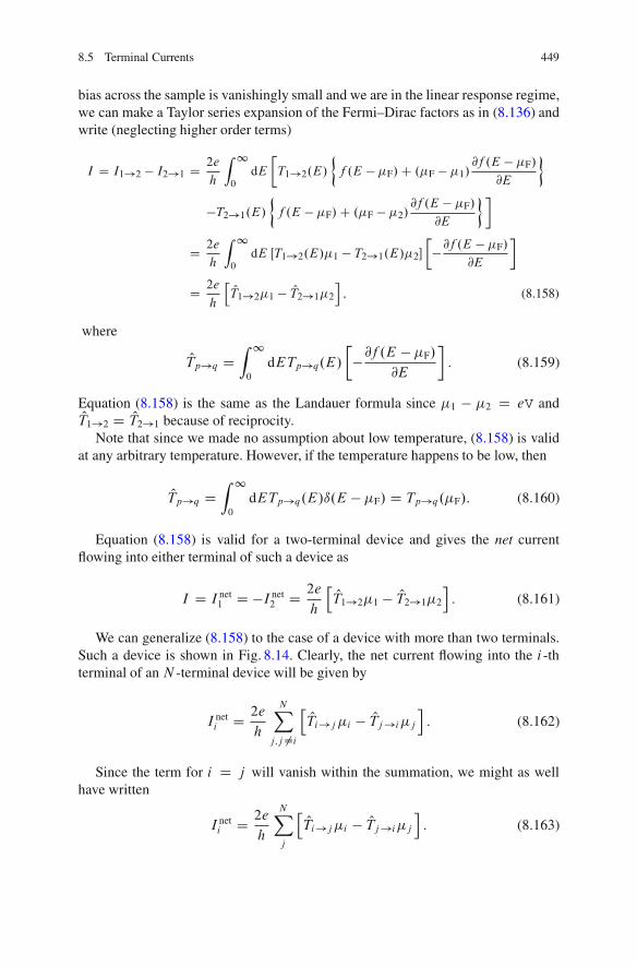
8.5 Terminal Currents 449
bias across the sample is vanishingly small and we are in the linear response regime,we can make a Taylor series expansion of the Fermi–Dirac factors as in (8.136) andwrite (neglecting higher order terms)
I D I1!2 � I2!1 D 2e
h
Z 1
0dE
T1!2.E/
�
f .E � �F/C .�F � �1/@f .E � �F/
@E
�
�T2!1.E/
�
f .E � �F/C .�F � �2/@f .E � �F/
@E
��
D 2e
h
Z 1
0dE ŒT1!2.E/�1 � T2!1.E/�2
�@f .E � �F/
@E
�
D 2e
h
h OT1!2�1 � OT2!1�2
i
; (8.158)
where
OTp!q DZ 1
0
dETp!q.E/
�@f .E � �F/
@E
�
: (8.159)
Equation (8.158) is the same as the Landauer formula since �1 � �2 D eV andOT1!2 D OT2!1 because of reciprocity.
Note that since we made no assumption about low temperature, (8.158) is validat any arbitrary temperature. However, if the temperature happens to be low, then
OTp!q DZ 1
0
dETp!q.E/ı.E � �F/ D Tp!q.�F/: (8.160)
Equation (8.158) is valid for a two-terminal device and gives the net currentflowing into either terminal of such a device as
I D I net1 D �I net
2 D 2e
h
h OT1!2�1 � OT2!1�2
i
: (8.161)
We can generalize (8.158) to the case of a device with more than two terminals.Such a device is shown in Fig. 8.14. Clearly, the net current flowing into the i -thterminal of an N -terminal device will be given by
I neti D 2e
h
NX
j;j¤i
h OTi!j�i � OTj!i�j
i
: (8.162)
Since the term for i D j will vanish within the summation, we might as wellhave written
I neti D 2e
h
NX
j
h OTi!j�i � OTj!i�j
i
: (8.163)

450 8 Quantum Transport Formalisms
I1 I2
I3I4
m1 m2
m3
m4
Fig. 8.14 A multiterminaldevice
At low temperatures,
I neti D 2e
h
NX
j;j¤i
Ti!j .�F/�i � Tj!i .�F/�j�
: (8.164)
If no magnetic field is present, then we can use the reciprocity relationTi!j .�F/ D Tj!i .�F/ and simplify the last equation to
I neti D 2e
h
NX
j;j¤iTi!j .�F/Œ�i � �j : (8.165)
For any given propagating mode or channel in the lead, the transmission fromone lead into all other leads, plus the reflection into the same lead must add up tounity. Thus, if there are M propagating channels or modes in the i -th lead, then
Ri!i .�F/CNT i!jX
j;j¤i.�F/ D M; (8.166)
where Ri!i is the reflection probability of an electron incident from the i -theterminal back into the i -th terminal.
Substituting this result into the preceding equation, we get that at low tempera-tures and voltages, the net current carried into the i -th terminal of a multi-terminaldevice is
I neti D 2e
h
2
4M � Ri!i .�F/�i �NX
j;j¤iTj!i .�F/�j
3
5: (8.167)
The last equation is due to Buttiker [25] and is known as Buttiker’s multiprobeformula. It expresses the current in any terminal of a phase coherent device as a

8.6 The 2-probe and 4-probe Landauer Formulas 451
function of the potentials at all other terminals and the transmission and reflectionprobabilities of electrons at the local Fermi levels in these terminals. Note that itshows immediately that any phase coherent device is intrinsically nonlocal in nature,since if we change the potential at any one terminal without changing anything else(e.g., carrier concentration in the device), then the currents at all other terminalswill change, which is the hallmark of nonlocality. This formula is very helpfulin understanding a number of phase-coherent phenomena, including an alternateexplanation for the integer quantum Hall effect, as we will see in the next chapter.
8.6 The 2-probe and 4-probe Landauer Formulas
Consider a 2-terminal device shown in Fig. 8.15a whose conductance is measuredby injecting a known current I from a current source into one of the terminals,extracting it from the other, and measuring the resulting potential difference Vbetween the same two terminals with a voltmeter. The conductance that we willmeasure in this 2-probe set up isG2-probe D I /V. We can also write this conductanceas G12;12 where Gij;kl represents the conductance measured with i; j as the currentprobes and k; l as the voltage probes. Let us see what the Buttiker multiprobeformula will predict for the 2-probe conductance of the device, assuming thattransport is phase coherent and we are in the linear response, low-temperatureregime.
We can write (8.164) in the matrix form
I1
I2
�
D 2e
h
T1!2 �T2!1
�T1!2 T2!1
� �1
�2
�
: (8.168)
Clearly, I1 D �I2 D I , and reciprocity dictates that T1!2 D T2!1 D T .Therefore, the last equation reduces to
I
�I�
D 2e
h
T �T�T T
� �1�2
�
; (8.169)
V
I
V
I
1 2
41
2 3
μ1 μ2 μ1 μ4
μ2 μ3
a b
Fig. 8.15 (a) A 2-probe setup, and (b) a 4-probe setup, for measuring conductance of a device

452 8 Quantum Transport Formalisms
which immediately yieldsI
�1 � �2 D 2e
hT : (8.170)
As always, we assume that the contacts are in local thermodynamic equilibriumcharacterized by chemical potentials�1 and �2 and that an electron equilibrates (bydissipation) immediately upon entering a contact. In that case, since the differencebetween the Fermi energies (or chemical potentials) in the two probes is the electroncharge times the applied voltage, i.e., �1 � �2 D eV, we get
G2-probe D G12;12 D I
VD 2e2
hT ; (8.171)
which is immediately recognized as the familiar Landauer formula in (8.144).Therefore, everything is consistent and appears to make sense.
Let us now investigate a slightly more complicated situation shown in Fig. 8.15bwhere we have a 4-probe set up for measuring conductance. Here, current is injectedinto one probe (probe 1), extracted from another (probe 4), while the resultingvoltage drop over the device is measured between two other probes (probes 2 and 3).The conductance of the device (between the latter two probes) is now given byG4-probe D G14;23 D I /V.
If we apply Buttiker’s multiprobe formula (8.167) to the latter scenario, we willget the following matrix equation:
2
664
I1I2I3
I4
3
775
D 2e
h
2
664
M � R1!1 �T2!1 �T3!1 �T4!1
�T1!2 M � R2!2 �T3!2 �T4!2
�T1!3 �T2!3 M �R3!3 �T4!3
�T1!4 �T2!4 �T3!4 M �R4!4
3
775
2
664
�1�2�3
�4
3
775:
(8.172)
Next, we will assume that the voltmeter connected between the two voltageprobes is an ideal voltmeter, which will draw no current and hence result in
I2 D �I3 D 0: (8.173)
Using the last condition in the immediately preceding equation, we get
ŒM � R2!2�2 D T1!2�1 C T3!2�3 C T4!2�4
ŒM � R3!3�3 D T1!3�1 C T2!3�2 C T4!3�4: (8.174)
Thereafter, using the result that I1 D �I4, we get
ŒM �R1!1�1 � T2!1�2 � T3!1�3 � T4!1�4
D �ŒM � R4!4�4 C T1!4�1 C T2!4�2 C T3!4�3: (8.175)

8.6 The 2-probe and 4-probe Landauer Formulas 453
Using the reciprocity relation Tij D Tj i , we can use (8.174) to express �1 and�4 in terms of �2 and �3 as follows:
�1 D Œ.M �R2!2/T3!4 C T2!3T2!4 �2 � Œ.M �R3!3/T2!4 C T2!3T3!4 �3
T1!2T3!4 � T1!3T2!4
�4 D Œ.M �R2!2/T1!3 C T1!2T2!3 �2 � Œ.M �R3!3/T1!2 C T1!3T2!3 �3
T1!3T2!4 � T1!2T3!4
:
(8.176)
Now, from (8.172), we obtain
I1 D 2e
hf.M � R1!1/�1 � T2!1�2 � T3!1�3 � T4!1�4g
D 2e
h
�
.M � R1!1/.M � R2!2/T3!4 C T2!3T2!4
T1!2T3!4 � T1!3T2!4
�
T1!4
.M � R2!2/T1!3 C T1!2T2!3
T1!3T2!4 � T1!2T3!4
� T1!2
�
�2
�
.M � R1!1/.M � R3!3/T2!4 C T2!3T3!4
T1!2T3!4 � T1!3T2!4
�
T1!4
.M � R3!3/T1!2 C T1!3T2!3
T1!3T2!4 � T1!2T3!4
� T1!3
�
�3
�
: (8.177)
The conductance measured in the 4-probe setup will be G4-probe D I=V DeI1=.�2 � �3/. Clearly, we can find this result from the last equation, and (8.175)and (8.176) that relate �2 to �3, but then the resulting expression for G4-probe willbe quite cumbersome (we leave it to the reader to work it out). A much simplerexpression can be obtained if we make the following assumptions:
1. First, we will assume that the voltage probes are weakly coupled to the device.It is as if there are tunnel barriers in leads 2 and 3 that make the transmissionprobability of electrons passing through these leads very small. Let us call thesetransmission probabilities , where ! 0, and assume that they are the same inleads 2 and 3 since these leads are nominally identical.
2. Next, we will assume that the current probes are strongly coupled to the device,i.e., there are no tunnel barriers in these probes and the probability of transmittingfrom these probes into the device is unity.
3. Finally, we will also assume that the bulk of the scattering encountered byelectrons going from one current probe (say, probe 1) to the other current probe(probe 4) is encountered in the region between the voltage probes, so that we canlump all scattering into one scatterer located between the voltage probes. Thisis shown by the shaded scatterer in Fig. 8.15b. Let the transmission probabilityassociated with traversing this scatterer be T .

454 8 Quantum Transport Formalisms
In that case, we can see that
T1!4 D TT1!2 D T3!4 D .M C R/T2!4 D T3!1 D TT2!3 D 2T ; (8.178)
where R is the reflection probability associated with reflection from the lumpedscatterer, and T C R D M . To understand where the preceding relations comefrom, consider the fact that an electron can reach probe 2 from probe 1 by eitherheading straight from 1 to 2 or by starting out from 1 toward probes 3 and 4,but then reflecting off the lumped scatterer with a probability R to journey towardprobe 2. Once the electron enters lead 2, it will ultimately emerge out of that leadby transmitting through the barrier in lead 2 with probability . Therefore, the totaltransmission probability T1!2 will be .M C R/. Similarly, an electron can reachprobe 4 from probe 2 in only one way: transmit through the barrier in lead 2 withprobability and then traverse the lumped scatterer with a probability T so thatT2!4 D T . Finally, an electron trying to reach probe 3 from probe 2 has an arduoustask. It has to transmit through lead 2 with the small probability , then transmitthrough the lumped scatterer with probability T and finally transmit through lead 3with small probability . Therefore, T2!3 D 2T , which is vanishingly small.
Using (8.178) in (8.177), and making use of the fact 1, we get
I1 D I � 2e
hMT 2.M C R/C 2T
.M C R/2 � T 2.�2 � �3/
D 2e2
h
TRV: (8.179)
Therefore, with all the three assumptions that we made, we end up with
G4-probe D G14;23 D I=V � 2e2
h
MTR D 2e2
h
MTM � T : (8.180)
Curiously, Landauer [26, 27] too had derived the last equation for the con-ductance of a device in phase coherent linear response transport, but withoutintroducing the 4-probe concept and without making all the assumptions that wemade. His derivation was very different from the one outlined here (it took intoaccount spatially localized electric fields caused by the scatterers), but neverthelessyielded the same final result as (8.180). The 2-probe result (8.144) or (8.171),on the other hand, was originally derived by Economou and Soukoulis [28], aswell as Fisher and Lee [29], who did not use the type of derivation that we haveused, but instead used the so-called Kubo formula which yields the linear response

8.6 The 2-probe and 4-probe Landauer Formulas 455
conductance based on an entirely different formalism. For some time, there wasimmense disagreement as to which formula—(8.171) or (8.180)—yields the correctlinear response conductance of a device when transport is phase coherent [30].
The first individuals to shed some slight on this matter were Engquist andAnderson [31] who introduced the notion of using a 4-probe setup—with separatecurrent and voltage leads—to justify (8.180). With this setup, they derived (8.180)while tacitly assuming weak coupling of the device to the voltage probes. Theirderivation was slightly different from the one outlined here which is reproducedfrom Buttiker [32], but the essential ingredients were similar. In the end, it is clearthat (8.180) refers to a 4-probe measurement with weakly coupled voltage probesand (8.171) refers to a 2-probe measurement. Hence, we will call the expressions inthese equations the 4- and 2-probe Landauer conductances, respectively, and theirreciprocals will be the 4- and 2-probe Landauer resistances.
8.6.1 The Contact Resistance
Transport experimentalists are very familiar with the fact that a two-terminalmeasurement of resistance never yields the true resistance of a device. Instead, ityields a resistance which is the sum of the true resistance and the so-called “contactresistance” Rcontact. The latter comes about because the leads and the device aredissimilar entities and therefore a junction resistance will inevitably materializewhere the two meet. However, a four-terminal measurement will eliminate thecontact resistance and yield the true resistance. In other words, we can roughly write
R2-probe D R4-probe CRcontact: (8.181)
Consider a perfect conductor that has no scatterer and transport through it iscompletely ballistic. The transmission probability through such a device is unityfor every channel and hence, if there are M propagating channels, then T D M .The 4-probe resistance of this device is R4-probe D 1=G4-probe D .h=2e2/Œ.M �T /=T D .h=2e2/Œ.M � M/=T D 0. This makes perfect sense. If there is noscatterer, there is nothing to “resist” the flow of current and hence the resistanceshould vanish. However, the 2-probe resistance is R2-probe D .h=2e2/Œ1=T D.h=2e2/Œ1=M , which does not vanish.
Substituting this result in (8.181), we immediately get that
Rcontact D h
2e21
M: (8.182)
The identification of the excess resistance (difference between the 2-probe and4-probe resistance formulas in the case of ballistic transport) as contact resistanceis due to Imry [33]. Therefore, the last equation gives an expression for the contactresistance in the linear response, phase coherent regime.

456 8 Quantum Transport Formalisms
r1 r2
T1
T1R2R1T2R2
R1
T1T2
(T , R )1 1 (T , R )2 2
Fig. 8.16 Two resistors r1 and r2 in series. Each resistor is represented as a lumped scatterercharacterized by a transmission and reflection probability (T, R). The ray diagram for finding theoverall transmission through the series combination is shown
8.6.2 The Addition Law of Series Resistance
All students of engineering and physics are very familiar with the addition law ofseries resistance. Consider two resistors r1 and r2 in series. Normally, we will expectthat the series resistance of the two will be r1 C r2. Assume now that each resistoris an ideal quantum wire with only one occupied subband so that there is a singlechannel for transport, or, in other words, a single propagating mode in each resistor.In the phase coherent regime, when the resistance of either resistor is given by theLandauer formula, we will show that indeed the series resistance of the two will ber1 C r2 if we use the 4-probe formula, but not if we use the 2-probe formula [34].This is a surprising result, but makes perfect sense.
In Fig. 8.16, we show two of the denumerably infinite number of so-calledFeynman paths for finding the transmission probability through the two resistorsin terms of the transmission and reflection probabilities associated with eachresistor. The Feynman paths depict the possible real space trajectories of an electrondetermined by multiple reflections. To find the total transmission through the seriescombination, we will merely sum the transmission probabilities associated witheach Feynman path. The reason why we will add the transmission probabilitiesand not the transmission amplitudes associated with these paths is that in thecontacts, the electrons thermalize (equilibrate with the contacts) and lose all phaseinformation. Therefore, we must add probabilities and not complex amplitudes thatcontain phase information. Clearly, the total transmission probability through theseries combination is
Tseries D T1�
1CR1R2 CR21R22 C : : : : : : : : :
�
T2
D T1T2
1 � R1R2: (8.183)

8.6 The 2-probe and 4-probe Landauer Formulas 457
Therefore,
1
TseriesD 1� R1R2
T1T2D 1 � .1 � T1/.1 � T2/
T1T2
D 1
T1C 1
T2� 1; (8.184)
where we have used the fact that Tn CRn D 1 for single-channeled transport.Now, if we use the 2-probe formula, then the series resistance will be
rseries D h
2e21
TseriesD h
2e21
T1C h
2e21
T2� h
2e2
D r1 C r2 � h
2e2¤ r1 C r2: (8.185)
We are off from the expected formula by the contact resistance of either resistor!In the 2-probe formula, we have implicitly included the contact resistance of eachresistor, so that we have counted it twice. Hence, we must subtract one contactresistance to get the correct result.
However, if we use the 4-probe formula, then the series resistance will be
rseries D h
2e21 � Tseries
TseriesD h
2e21 � T1
T1C h
2e21 � T2T2
D r1 C r2; (8.186)
which is the expected result. The 4-probe formula always yields the expected seriesresistance since, in this case, there is no issue of the contact resistance.
In (8.184), the quantities T1 and T2 can be viewed as the transmission probabili-ties through two sections of a resistor of lengths L1 and L2, respectively, while thetotal length of the resistor is L D L1 C L2. Therefore, we can rewrite (8.184) as
1
TLD 1
TL1C 1
TL2� 1; (8.187)
If we are seeking an expression for the transmission probability through a sectionas a function of its length, the following function satisfies the last equation:
T .L/ D L0
LC L0; (8.188)
whereL0 is the length at which the transmission probability becomes 0.5. What thisexpression shows is that at small length L L0, the transmission probability isindependent of L and nearly unity, while for large length L � L0, the transmissionprobability falls off as the inverse of the length L.

458 8 Quantum Transport Formalisms
8.6.3 Computing the Landauer Resistances by Findingthe Transmission Probability Through a Device
A truly wonderful feature of the Landauer formulas is that in order to find eitherthe 2- or the 4-probe Landauer resistance6 of a device in linear response and atlow temperatures, all that we need to know is the total transmission probability ofelectrons that are at the Fermi level in the contacts. Therefore, we need a handyprescription to find this quantity.
The transmission probability through the device can be generally found bysolving the Schrodinger equation in a one-dimensional spatially varying potentialwhich includes elastic scattering potentials and all other potentials due to externalelectric fields and space charges. The potential varies spatially in the directionof transmission, or current flow. Equation (3.93) provides the transmission am-plitude tk for an electron incident on the device from the injecting contact withwavevector k . Since the matrix elements Wpq are always purely real [35], we canwrite
T .k/ D jtkj2 D 4k2
k2.W11 CW22/2 C .W12k2 �W21/2: (8.189)
The last relation gives us the transmission probability of any electron incidentwith wavevector k on a device containing a spatially varying potential in thedirection of current flow. In order to find the Landauer resistances of such a device,we need to find the transmission probabilities of an electron at the Fermi energyEF
for every propagating mode, i.e., for every occupied subband in the leads. We willcall these probabilities Tp;q , where p and q are the subband indices in the leads.
We proceed by first finding the wavevector kp;q for an electron at the Fermi levelin the .p; q/-th subband by using the relation
EF D „2k2p;q2ml
C p;q; (8.190)
where p;q is the energy at the bottom of the .p; q/-th subband andml is the effectivemass of an electron in the leads.7 We then set k D kp;q in (8.189) to find Tpq , andfrom that we can find the total transmission probability T of all propagating modesat the Fermi level since T D Ppropagating modes
p;q Tpq . This then allows us to find theLandauer resistances of any device containing a spatially varying potential in thedirection of current flow.
6Whenever we mention 4-probe Landauer resistance, we tacitly imply that the probes are weaklycoupled to the device so that the 4-probe formula is valid.7The quantity p;q is of course found from the geometry and transverse dimensions of the leads.For example, if the cross-section of the leads is a rectangle of dimensions Wy and Wz, then p;q D.„2=2ml /Œ.p�=Wy/
2 C .q�=Wz/2.

8.7 The Landau–Vlasov Equation... 459
8.7 The Landau–Vlasov Equation or the CollisionlessQuantum Boltzmann Transport Equation
So far, we have described quantum transport in the framework of the Schrodingerequation, which is very different from the Boltzmann formalism that we used todescribe classical transport in Chap. 2. In Boltzmann formalism, we solve the BTEto find the classical Boltzmann distribution function whose various moments aretransport variables, such as carrier concentration, current density, etc. It is thereforenatural to ask if there is a quantum-mechanical equivalent of the BTE whichwill yield perhaps a “quantum-mechanical distribution function” whose momentsmight yield transport variables. The answer to that question is “yes,” but beforewe examine this further, let us revisit the reasons why the Boltzmann distributionfunction cannot describe phase coherent quantum phenomena.
The Boltzmann distribution function is fundamentally a classical construct.It is a “probability” and hence always positive indefinite, i.e., its value can bepositive or zero, but never negative. Such a quantity will be incapable of describingquantum-mechanical phenomena like destructive interference where two nonzerodistribution functions will have to superpose to produce a null since at the point ofdestructive interference, the probability of finding an electron should vanish. Thatcan only happen if one of the distribution functions has a positive value and theother a negative value. But negative values are not permissible for the Boltzmanndistribution function, which is why it can never describe quantum reality. Of coursethe Boltzmann distribution function has other shortcomings too. It is simultaneouslya function of spatial and wavevector coordinates Er and Ek, which is not permissiblein the quantum world since Er and Ek are Fourier transform pairs and therefore mustobey the Heisenberg Uncertainty relation�Er ��Ek � 1=2.
It is, however, possible to define an alternate quantum-mechanical function thatobeys an equation which looks like the BTE mathematically. Such a function willnot be positive indefinite and will not even necessarily be a real quantity, which isperfectly fine since it will not have anything to do with “probability.” The equationthat describes the evolution of this function in time t , real space Er and wavevectorspace Ek has exactly the same mathematical appearance as the BTE, except that theright-hand side is zero. Since the right-hand side of the BTE gives us the time rateof change of the distribution function due to collisions, this equation will have theappearance of the collisionless BTE describing ballistic transport. Therefore, it issometimes referred to as the “collisionless quantum BTE.” Landau and Vlasov hadused this equation extensively to study ballistic transport in plasmas, which is whyit is also sometimes referred to as the Landau–Vlasov equation. We will derive itnext.
Let us start with the Schrodinger equation governing a single electron in a time-and space-dependent potential. It is
i„@ .Er; t/@t
D
� „22m� r2 C V.Er; t/
�
.Er; t/: (8.191)

460 8 Quantum Transport Formalisms
We can treat the potential V.Er; t/ as a perturbation, so that the unperturbedwavefunctions are the free electron wavefunctions
0.Er; t/ D 1p˝
ei�Ek0�Er�Ek0
t=„�
; (8.192)
where
Ek0 D „2k02
2m� : (8.193)
The perturbed wavefunctions can be written as usual:
.Er; t/ DX
Ek0
CEk0
.t/1p˝
ei�Ek0�Er�Ek0
t=„�
DX
Ek0
CEk0
.t/1p˝
eiEk0�Er ; (8.194)
where
CEk0
.t/ D CEk0
.t/e�iEk0t=„: (8.195)
Substituting (8.194) in (8.192), we get
i„XEk0
@CEk0
.t /
@t
1p˝
eiEk0
�Er D X
Ek0
CEk0
.t /
� „22m�
r2
�1p˝
eiEk0
�Er CX
Ek0
V .Er; t /CEk0
.t /1p˝
eiEk0
�Er
D X
Ek0
CEk0
.t /Ek0
1p˝
eiEk0
�Er CX
Ek0
V .Er; t /CEk0
.t /1p˝
eiEk0
�Er :
(8.196)
If we multiply the last equation throughout by 1p˝
e�iEk�Er , integrate over all spaceand use the orthonormality condition
Z 1
0
d 3Er 1p˝
e�iEk�Er 1p˝
eiEk0�Er DZ 1
0
d 3Er 1˝
e�i.Ek�Ek0/�Er D 1
˝ı.Ek � Ek0/ D ıEk;Ek0
;
(8.197)
where the first delta is a Dirac delta function and the last one is a Kronecker delta,then we get
i„X
Ek0
@CEk0
.t/
@tıEk;Ek0
DX
Ek0
CEk0
.t/Ek0ıEk;Ek0
CX
Ek0
CEk0
.t/1
˝
Z 1
0
d 3ErV .Er; t/e�i.Ek�Ek0/�Er
DX
Ek0
CEk0
.t/Ek0ıEk;Ek0
CX
Ek0
CEk0
.t/VEk�Ek0
.t/; (8.198)

8.7 The Landau–Vlasov Equation... 461
where
VEk�Ek0
.t/ D 1
˝
Z 1
0
d 3ErV .Er; t/e�i.Ek�Ek0/�Er : (8.199)
This quantity is the Fourier component of the potential V.Er; t/ at the wavevectorEk � Ek0
In (8.200), the Kronecker delta will remove the summations, so that this equationreduces to
@CEk.t/@t
C i
„CEk.t/Ek DX
Ek0
CEk0
.t/VEk�Ek0
.t/
i„ : (8.200)
Taking the complex conjugate of both sides, we obtain
@C �Ek .t/@t
� i
„C�Ek .t/Ek D �
X
Ek0
C �Ek0
.t/V �
Ek�Ek0
.t/
i„ : (8.201)
Now, the potential V.Er; t/ had to have been a real quantity since the Hamiltonianmust always be Hermitian. Therefore, V �
Ek�Ek0
.t/ D V �Ek0�Ek.t/, which yields
@C �Ek .t/@t
� i
„C�Ek .t/Ek D �
X
Ek0
C �Ek0
.t/VEk0�Ek.t/
i„ : (8.202)
Multiplying the last equation by CEkCEq.t/, where Eq is an arbitrary wavevector, weobtain
@C �Ek .t/@t
CEkCEq.t/ � i
„C�Ek .t/CEkCEq.t/Ek D �
X
Ek”
C �Ek”.t/CEkCEq.t/
VEk”�Ek.t/i„ : (8.203)
where we have replaced Ek0 with Ek” since both Ek0 and Ek” are dummy variables forsummation.
Since (8.200) is valid for any arbitrary wavevector Ek, we can replace Ek with EkC Eqin this equation to get
@CEkCEq.t/@t
C i
„CEkCEq.t/EjEkCEqj DX
Ek0
CEk0
.t/VEkCEq�Ek0
.t/
i„ : (8.204)
Multiplying the last equation throughout by C �Ek .t/, we obtain
C �Ek .t/
@CEkCEq.t/@t
C i
„C�Ek .t/CEkCEq.t/EjEkCEqj D
X
Ek0
C �Ek .t/CEk0
.t/VEkCEq�Ek0
.t/
i„ :
(8.205)

462 8 Quantum Transport Formalisms
Adding (8.203) and (8.205), we find
@h
C�Ek .t/CEkCEq.t/
i
@tC i
„C�Ek .t/CEkCEq.t/
h
EjEkCEqj �Ek
i
DX
Ek0
C�Ek .t/CEk0
.t/VEkCEq�Ek0
.t/
i„ �X
Ek”
C�Ek”.t/CEkCEq.t/
VEk”�Ek.t/i„ :
(8.206)
Since both Ek0 and Ek” are dummy variables for summation, let
Ek0 D Ek C Eq � Eq0
Ek” D Ek C Eq0: (8.207)
This will make Eq0 the new dummy variable for summation.With the last variable transformations, (8.206) becomes
@h
C �Ek .t/CEkCEq.t/
i
@tC i
„C�Ek .t/CEkCEq.t/
h
EjEkCEqj � Ek
i
DX
Eq0
VEq0.t/
i„h
C �Ek .t/CEkCEq�Eq0
.t/ � CEkCEq.t/C�EkCEq0
.t/i
: (8.208)
Now, define a quantum correlation function Of�Ek1; Ek2; t
�
as
Of .Ek1; Ek2; t/ D C �Ek1.t/CEk2CEk1.t/: (8.209)
With this definition, (8.208) becomes
@ Of .Ek; Eq; t/@t
C i
„Of .Ek; Eq; t/
h
EjEkCEqj �Ek
i
DX
Eq0
VEq0.t/
i„ Œ Of .Ek; Eq � Eq0; t/ � Of .Ek C Eq; Eq � Eq0; t/: (8.210)
We can now make a Taylor series expansion of the energyEjEkCEqj and write it as
EjEkCEqj D Ek C Eq � ErEkEk C jEqj22Š
r2kEk C : : : : (8.211)
If jEqj jEkj, then we can neglect the second and higher order terms involving jEqjin the Taylor expansion and write
EjEkCEqj � Ek � Eq � ErEkEk: (8.212)

8.7 The Landau–Vlasov Equation... 463
Similarly, using Taylor series expansion, we find that for small Eq,
Of .Ek; Eq � Eq0; t/ � Of .Ek C Eq; Eq � Eq0; t/ � �Eq � ErkOf .Ek; Eq � Eq0; t/: (8.213)
Equation (8.210) can then be written as
@ Of .Ek; Eq; t/@t
C
iEq � 1„ErkEk
�
Of .Ek; Eq; t/ DX
Eq0
iEq VEq0.t/
„ � ErkOf .Ek; Eq� Eq0; t/: (8.214)
or
@ Of .Ek; Eq; t/@t
C iEq � Evk Of .Ek; Eq; t/ D iEq VEq0.t/
„ ˝ ErkOf .Ek; Eq; t/: (8.215)
where ˝ denotes the convolution operation and Evk D 1„ ErkEk.
We now take the inverse Fourier transform of both sides of the precedingequation, i.e., we multiply both sides by eiEq�Er and integrate over all Eq, to obtain
@ Of .Ek; Er; t/@t
C Evk � ErrOf .Ek; Er; t/ D
ErrV.Er; t/„ � Erk
Of .Ek; Er; t/; (8.216)
where
Of .Ek; Er; t/ DZ
d3EqeiEq�Er Of .Ek; Eq; t/: (8.217)
Since force is the negative gradient of potential energy, we can write
EF .Er; t/ D � ErrV.Er; t/; (8.218)
which will reduce the preceding equation to
@ Of .Er; Ek; t/@t
C Evk � ErrOf .Er; Ek; t/C
EF .Er; t/„ � Erk
Of .Er; Ek; t/ D 0: (8.219)
The last equation has the same appearance as the BTE. Instead of the “distri-bution function,” we have the quantum correlation function Of .Er; Ek; t/. The latteris not the quantum-mechanical probability of finding at electron at position Er withwavevector Ek at time t . It is not positive indefinite and clearly can be complex (notreal). It is also a quantum-mechanically legitimate function since Ek and Er are notFourier transform pairs and therefore do not obey the uncertainty relation (Eq and Erare Fourier transform pairs, but Eq is not Ek).
It may seem that since the right-hand side is zero, this equation can onlyapply to the collisionless regime. That is actually not entirely correct since elastic(nondissipative) scattering caused by impurities can be incorporated in the potentialV.Er; t/ as a scattering potential, as long as the potential is varying slowly in space.

464 8 Quantum Transport Formalisms
The slow variation is required since we assumed in the derivation that the Fouriertransform of the position variable Er , i.e. the quantity Eq, is small. That assumption isvalid as long as all potentials are varying slowly in space so that they have no largewavevector (Fourier) components.
The correlation function Of .Er; Ek; t/ does obey the collisionless BTE, but it is notimmediately obvious what its use might be. We can actually formulate a quantumcorrelation function in a different way so that it will not only obey the collisionlessBTE but its zeroth moment will give the expectation value of the particle density andthe first moment will give the expectation value of the current density at positionEr at time t . Such a function will be an exact quantum-mechanical analog of theBoltzmann distribution function. We proceed to derive this quantum correlationfunction and show that it obeys the collisionless BTE.
8.8 A More Useful Collisionless Boltzmann TransportEquation
The Schrodinger equation for a particle with wavefunction .Er1; t/ is
i„@ .Er1; t/@t
D H.Er1; t/ .Er1; t/: (8.220)
Multiplying the above equation throughout by the wavefunction �.Er2; t/, weobtain
i„ �.Er2; t/@ .Er1; t/@t
D H.Er1; t/Œ .Er1; t/ �.Er2; t/: (8.221)
where the Hamiltonian H.Er1; t/ does not act on �.Er2; t/ since the former is afunction of Er1 and the latter is a function of Er2.
Similarly, the Schrodinger equation for a particle with wavefunction .Er2; t/ is
i„@ .Er2; t/@t
D H.Er2; t/ .Er2; t/: (8.222)
which, upon complex conjugation, becomes
� i„@ �.Er2; t/@t
D H.Er2; t/ �.Er2; t/: (8.223)
where we have used the fact that H�.Er2; t/ D H.Er2; t/ since the Hamiltonian ishermitian as long as there is no dissipation.
Multiplying the last equation throughout by � .Er1; t/ yields
i„ .Er1; t/@ �.Er2; t/@t
D �H.Er2; t/Œ .Er1; t/ �.Er2; t/: (8.224)
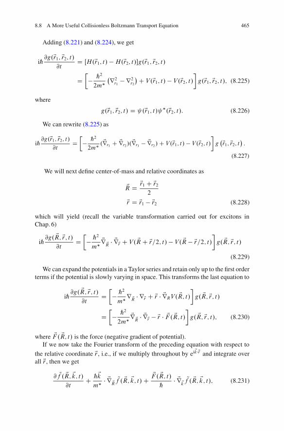
8.8 A More Useful Collisionless Boltzmann Transport Equation 465
Adding (8.221) and (8.224), we get
i„@g.Er1; Er2; t/@t
D ŒH.Er1; t/ �H.Er2; t/g.Er1; Er2; t/
D
� „22m�
�r2r1
� r2r2
�C V.Er1; t/ � V.Er2; t/�
g.Er1; Er2; t/; (8.225)
where
g.Er1; Er2; t/ D .Er1; t/ �.Er2; t/: (8.226)
We can rewrite (8.225) as
i„@g.Er1; Er2; t/@t
D
� „22m�
. Err1 C Err2 /.Err1 � Err2 /C V.Er1; t/ � V.Er2; t/
�
g�Er1; Er2; t
�
:
(8.227)
We will next define center-of-mass and relative coordinates as
ER D Er1 C Er22
Er D Er1 � Er2 (8.228)
which will yield (recall the variable transformation carried out for excitons inChap. 6)
i„@g.ER; Er; t/@t
D
� „2m� Er ER � ErEr C V. ERC Er=2; t/� V. ER � Er=2; t/
�
g. ER; Er; t/
(8.229)
We can expand the potentials in a Taylor series and retain only up to the first orderterms if the potential is slowly varying in space. This transforms the last equation to
i„@g.ER; Er; t/@t
D
� „2m� r ER � rEr C Er � ErRV. ER; t/
�
g. ER; Er; t/
D
� „22m� Er ER � ErEr � Er � EF . ER; t/
�
g. ER; Er; t/; (8.230)
where EF . ER; t/ is the force (negative gradient of potential).If we now take the Fourier transform of the preceding equation with respect to
the relative coordinate Er , i.e., if we multiply throughout by eiEk�Er and integrate overall Er , then we get
@ Qf . ER; Ek; t/@t
C „Ekm� � Er ER Qf . ER; Ek; t/C
EF . ER; t/„ � ErEk Qf . ER; Ek; t/; (8.231)

466 8 Quantum Transport Formalisms
where
Qf . ER; Ek; t/ DZ
d3Ere�iEk�Erg. ER; Er; t/: (8.232)
In other words, the correlation function Qf . ER; Ek; t/ is the Fourier transform ofg. ER; Er; t/ with respect to the relative coordinate Er .
Note that the new correlation function Qf . ER; Ek; t/ not only obeys an equation thatlooks identical with the collisionless BTE but it is a very meaningful function. If weintegrate this function over all wavevector, then from (8.232), we get
Z
d3 Ek Qf . ER; Ek; t/ DZ
d3ErZ
d3 Eke�iEk�Er�
g. ER; Er; t/
DZ
d3Erı.Er/g. ER; Er; t/
D g. ER; 0; t/D . ER; t/ �. ER; t// n. ER; t/: (8.233)
Therefore, the zeroth moment of the new correlation function gives the particledensity. Similarly, it can be shown that the first moment gives the particle currentdensity [36]. In other words, this new correlation function is an exact quantum-mechanical analog of the Boltzmann distribution function. Its shortcoming, how-ever, is that it can only describe ballistic transport or transport in the presence ofslowly varying elastic scattering potentials which do not cause dissipation. If wewish to incorporate dissipation into our quantum transport model, then that becomesa seriously difficult task, which we address next.
8.9 Quantum Correlations
Consider an electron interacting with a spatially and temporally varying potential,as in a real device. Its wavefunction can be expanded in a complete orthonormal set(recall Chap. 3 material):
.Er; t/ D 1p˝
X
EkCEk.t/e
iEk�Er : (8.234)
We can define a density matrix as
�Ek;Ek0
.t/ D C �Ek .t/CEk0
.t/; (8.235)

8.9 Quantum Correlations 467
where, as usual, the asterisk denotes complex conjugate. In the full matrix form, thedensity matrix will be written as
Œ�.t/ D
2
66666666664
C �Ek1.t/CEk1.t/ C �
Ek1.t/CEk2 .t/ : : : : : : : : : C �Ek1.t/CEkn.t/
C �Ek2.t/CEk1.t/ C �
Ek2.t/CEk2 .t/ : : : : : : : : : C �Ek2.t/CEkn.t/
: : : : : : : : : : : : : : : : : :
: : : : : : : : : : : : : : : : : :
: : : : : : : : : : : : : : : : : :
C �Ekn.t/CEk1.t/ C �
Ekn.t/CEk2.t/ : : : : : : : : : C �Ekn.t/CEkn.t/
3
77777777775
:
(8.236)
Clearly, a diagonal element C �Ekm.t/CEkm.t/ D jCEkm j2.t/ is the probability of
finding the electron in the wavevector state Ekm with wavefunction .1=p˝/eiEkm�Er at
time t , and is the Boltzmann distribution function f .Ekm; t/. The diagonal elementsare all positive indefinite and real. The off-diagonal elements, on the other hand, giveus the phase correlations between the different amplitudes. They can be complexquantities and are not positive indefinite. Therefore, the density matrix containsmore information than the Boltzmann distribution function since the off-diagonalterms contain additional information which the Boltzmann distribution functiondoes not have. Moreover, the density matrix is also inherently quantum-mechanicalin nature since the phase relations between the different wavevector states is aquantum-mechanical attribute. Note that while the diagonal terms of the densitymatrix provide information about auto-correlations between the same wavevectorstates, the off-diagonal terms provide information about cross-correlations betweendifferent wavevector states.
Instead of working with amplitudes in wavevector space, we could have also usedamplitudes in real space and written them as CEr .t/ instead of CEk.t/, so that (8.234)would have transformed to
.Er; t/ D 1p˝
X
ErCEr .t/eiEk�Er : (8.237)
We can then define a correlation function
� iG<.Er1; t1I Er2; t2/ DD
C �Er1 .t1/CEr2.t2/
E
; (8.238)
where i is the usual imaginary square-root of �1 and the brackets denote ensembleaveraging over all the available states of the system, regardless of whether thesystem is in equilibrium or nonequilibrium. Note that this function tells us thecorrelation between the amplitude at position Er1 at time t1 and the amplitude atposition Er2 at time t2.

468 8 Quantum Transport Formalisms
Next, we can define center-of-mass and relative coordinates in the usual fashion:
ER D Er1 C Er22
Er D Er1 � Er2T D t1 C t2
2
t D D t1 � t2; (8.239)
and write the correlation function as
� iG<.Er1; t1I Er2; t2/D � iG<. ER; T I Er; t/DD
C �ERCEr=2.T C t=2/C ER�Er=2.T � t=2/
E
:
(8.240)
Then we Fourier transform the relative variables Er and t into Ek and !, so that weobtain a new correlation functionW.Ek; ER;!; T / given by:
W.Ek; ER;!; T / D �iZ
d3Ere�iEk�ErZ
dte�i!tG<. ER; T I Er; t/
DZ
d3Ere�iEk�ErZ
dte�i!tD
C �ERCEr=2.T C t=2/C ER�Er=2.T � t=2/
E
:
(8.241)
This transformation is called the Wigner–Weyl transformation and the functionW.Ek; ER;!; T / is called the Wigner distribution function.
If we integrate the Wigner distribution function over all wavevector and fre-quency, then we get
Zd3 Ek.2�/3
Zd!
2�W. Ek; ER;!; T / D
Z
d3ErZ
dt
"Z
d3 Ek.2�/3
e�iEk�Er#Z
d!
2�e�i!t
�
�D
C�ERCEr=2.T C t=2/C ER�Er=2.T � t=2/
E
DZ
d3ErZ
dtı.Er/ı.t/C�ERCEr=2.T C t=2/C ER�Er=2.T � t=2/
DD
C�ER.T /C ER.T /
E
D�ˇˇˇC ER.T /
ˇˇˇ
2�
D �iG<. ER; T I ER; T /; (8.242)

8.9 Quantum Correlations 469
The quantity hjC ER.T /j2i is the probability of finding an electron at position ER attime T averaged over all available states of the system. Therefore, it is clearlyproportional to the carrier concentration at position ER at time T . Consequently, wecan write
n. ER; T / / �iG<. ER; T I ER; T / DZ
d3 Ek.2�/3
Zd!
2�W.Ek; ER;!; T /: (8.243)
The Wigner distribution function W.Ek; ER;!; T / is therefore also a quantummechanical analog of the Boltzmann distribution function, since integrating it overall wavevector and all frequencies yields the carrier concentration. In fact, it canalso be shown that the current density at position ER at time T is given by
EJ . ER; T / / �eZ
d3 Ek.2�/3
Zd!
2�
"
„Ek � e EA. ER; T /m�
#
W.Ek; ER;!; T /; (8.244)
where EA. ER; T / is a vector potential, due to such things as a magnetic field, atlocation ER and time T . Therefore, the carrier concentration is like the zerothmoment and the current density is like the first moment of the Wigner distributionfunction. This is as far as the analogy between the Wigner function and theBoltzmann distribution function goes. The Wigner function does not satisfy anequation that looks like the BTE (unlike the correlation function Qf .Er; Ek; t/), nor isit positive indefinite, nor does it violate the Heisenberg uncertainty principle sinceneither the pair . ER; Ek/ nor the pair (!, t) are Fourier transform pairs.
The reader can easily show that if we are interested in finding the carrierconcentration at a particular energy E , or correspondingly at a particular frequency! (E D „!), then we will not be carrying out the integration over ! and the resultwill be
n.!;R; T / /Z
dte�i!tD
C�ER.T C t=2/C ER.T � t=2/
E
D �iZ
dte�i!tG<. ER;T C t=2I ER; T � t=2/ D �iZ
dte�i!tG<. ER; t1IR; t2/
D �iG<. ER; T; ER;!/: (8.245)
Similarly, the current density at a particular frequency ! will be
EJ .!; ER; T / / e„m�
h ErR � ErR0
i
G<. ER;T; ER0; !/ˇˇˇ ERD ER0
� ie2
m� EA. ER;T /G<. ER;T; ER;!/:(8.246)
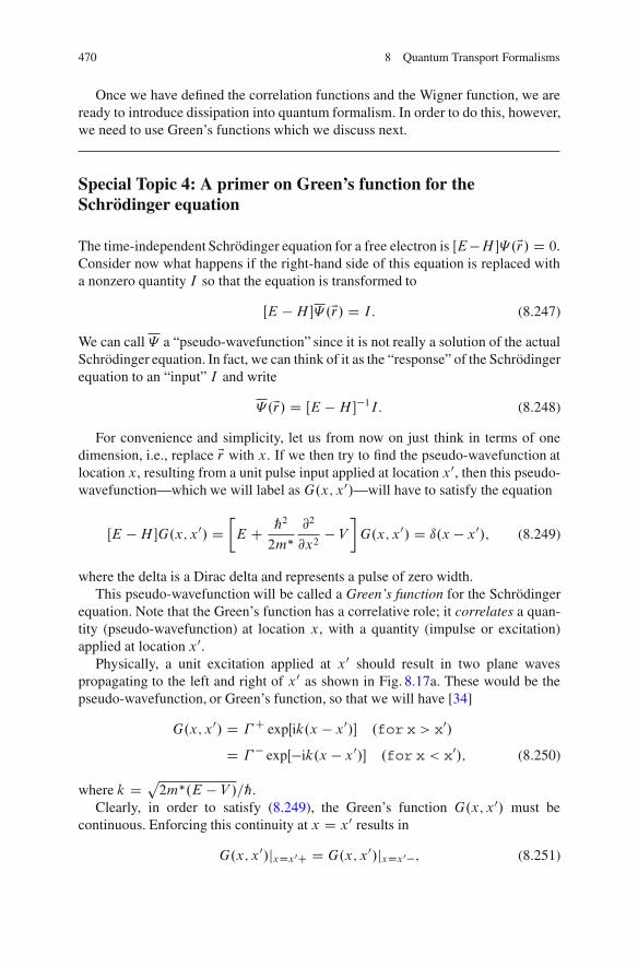
470 8 Quantum Transport Formalisms
Once we have defined the correlation functions and the Wigner function, we areready to introduce dissipation into quantum formalism. In order to do this, however,we need to use Green’s functions which we discuss next.
Special Topic 4: A primer on Green’s function for theSchrodinger equation
The time-independent Schrodinger equation for a free electron is ŒE�H .Er/ D 0.Consider now what happens if the right-hand side of this equation is replaced witha nonzero quantity I so that the equation is transformed to
ŒE �H .Er/ D I: (8.247)
We can call a “pseudo-wavefunction” since it is not really a solution of the actualSchrodinger equation. In fact, we can think of it as the “response” of the Schrodingerequation to an “input” I and write
.Er/ D ŒE �H�1I: (8.248)
For convenience and simplicity, let us from now on just think in terms of onedimension, i.e., replace Er with x. If we then try to find the pseudo-wavefunction atlocation x, resulting from a unit pulse input applied at location x0, then this pseudo-wavefunction—which we will label as G.x; x0/—will have to satisfy the equation
ŒE �HG.x; x0/ D
E C „22m�
@2
@x2� V
�
G.x; x0/ D ı.x � x0/; (8.249)
where the delta is a Dirac delta and represents a pulse of zero width.This pseudo-wavefunction will be called a Green’s function for the Schrodinger
equation. Note that the Green’s function has a correlative role; it correlates a quan-tity (pseudo-wavefunction) at location x, with a quantity (impulse or excitation)applied at location x0.
Physically, a unit excitation applied at x0 should result in two plane wavespropagating to the left and right of x0 as shown in Fig. 8.17a. These would be thepseudo-wavefunction, or Green’s function, so that we will have [34]
G.x; x0/ D � C expŒik.x � x0/ .for x > x0/
D � � expŒ�ik.x � x0/ .for x < x0/; (8.250)
where k D p
2m�.E � V /=„.Clearly, in order to satisfy (8.249), the Green’s function G.x; x0/ must be
continuous. Enforcing this continuity at x D x0 results in
G.x; x0/jxDx0C D G.x; x0/jxDx0�; (8.251)

8.9 Quantum Correlations 471
unit excitation
x = x’
ΓΓ+-
unit excitation
x = x’
ΓΓ+-
a
b
Fig. 8.17 Unit excitation applied at location x0 causes two waves to travel (a) outwards, or (b)inwards
or
� C D � �: (8.252)
The first derivatives of the Green’s function are
@G.x; x0/@x
ˇˇˇˇxDx0�
D � limx!x0
� �ik exp �ik.x � x0/
� D �ik� �
@G.x; x0/@x
ˇˇˇˇxDx0C
D limx!x0
� Cik exp
ik.x � x0/� D ik� C: (8.253)
Therefore,
@G.x; x0/@x
ˇˇˇˇxDx0C
� @G.x; x0/@x
ˇˇˇˇxDx0�
D ik
� C C � �� : (8.254)
From (8.249), we get
„22m�
@2G.x; x0/@x2
D ı.x � x0/� .E � V /G.x � x0/: (8.255)

472 8 Quantum Transport Formalisms
Integrating the above equation over x between the limit x� and xC, we obtain
„22m�
Z x0C
x0�@2G.x; x0/
@x2dx D
Z x0C
x0�ı.x � x0/dx � .E � V /
Z x0C
x0�G.x � x0/dx
D 1 � .E � V /ŒG.x; x0/jxDx0C �G.x; x0/jxDx0�
D 1 � .E � V /Œ� C � � �
D 1; (8.256)
since � C D � �.Therefore, from (8.254) and the previous equation, we obtain
@G.x; x0/@x
ˇˇˇˇxDx0C
� @G.x; x0/@x
ˇˇˇˇxDx0�
D ik
� C C � �� D 2m�
„2 : (8.257)
From (8.252) and (8.257), we obtain
� C D � � D � i
„v; (8.258)
where v D „k=m�.Using the last result in (8.250), we get
G.x; x0/ D � i
„vexpŒikjx � x0j: (8.259)
Now, the unit excitation introduced at x0 can also cause two plane waves to traveltoward the location x0, rather than away from it [34]. This is shown in Fig. 8.17b.This situation would give rise to an alternate solution for the Green’s function:
G.x; x0/ D i
„vexpŒ�ikjx � x0j: (8.260)
The first solution is called the retarded Green’s function GR.x; x0/ and thesecond is the advanced Green’s functionGA.x; x0/. The difference between the twois that the former corresponds to outgoing waves and the latter to incoming waves.Note that one is complex conjugate or Hermitian conjugate of the other:
GR.x; x0/ D GA.x; x0/�: (8.261)
where the “dagger” represents Hermitian conjugate.Which solution—the retarded or the advanced—is the acceptable solution for the
Green’s function can be decided by adding an arbitrary imaginary component to theenergy of the electron [34]. This will transform (8.249) to
ŒE�HCi�G.x; x0/ D
E C „22m�
@2
@x2� V C i�
�
G.x; x0/ D ı.x�x0/: (8.262)

8.10 Quantum Transport in an Open System with Device-Contact Coupling... 473
The wavevector k now becomes
k0 Dp
2m�.E � V C i�/
„ Dp
2m�.E � V /„
r
1C i�
E � V� k
1C i�
2.E � V /�
D k.1C iı/; (8.263)
where ı D �
2.E�V / . In that case,
GR.x; x0/ D � i
„vexp
�ıjx � x0j C ikjx � x0j�
GA.x; x0/ D i
„vexp
ıjx � x0j � ikjx � x0j� : (8.264)
In this case, the retarded Green’s function is the only acceptable solution if �;ı > 0, because then the retarded function is a decaying wave and the advancedfunction is a growing (and hence unphysical) wave. On the other hand, if �; ı < 0,then the advanced Green’s function is the only acceptable solution.
The preceding primer on Green’s function is adapted from [34].
8.10 Quantum Transport in an Open System withDevice-Contact Coupling and the Self-Energy Potential
In the Tsu–Esaki formalism, or the Landauer–Buttiker formalism, we have alwaysviewed the device as a phase-coherent or dissipationless entity. All dissipation (lossof phase coherence) is assumed to take place in the contacts. Once an electron entersa contact, it immediately thermalizes and reaches equilibrium with its surroundingssince the contact is an infinite reservoir whose equilibrium cannot be disturbed. Thisviewpoint ensures that Fermi–Dirac statistics is maintained in the contacts with aparticular Fermi energy or chemical potential �. The question that inevitably arisesis how can one merge the dissipative contacts and the nondissipative device intoone comprehensive description where there is two-way communication between thedevice and the contacts. It is not just that the contacts inject and extract carriersfrom the device while the device does nothing to the contacts; instead both affectone another.
If we view the device as a closed system that does not exchange electrons withthe contacts, then the device would be the proverbial “box” in the particle-in-a-boxdescription that we see in elementary quantum mechanics. The boundaries of thedevice will act as impenetrable infinite potentials or “hard walls” and the energyof an electron inside the device can assume only discrete values. However, if we

474 8 Quantum Transport Formalisms
couple the device to the contact in a manner that the device can exchange electronswith the contacts, then the discrete energy levels will broaden. Phenomenologically,the amount of broadening will be given by the Heisenberg uncertainty relation andwill be of the order of „=� , where 1=� is the rate at which an electron is enteringor exiting into a contact. Such a system is an open system where particles areexchanged between contacts and the device.
8.10.1 Coupling of a Device to a Single Contact
To start with, let us focus on the simplest open system consisting of the device andone (not two) contact. In this case, there will be no current flow since we do not havetwo contacts to inject and extract electrons, and the device and contact will alwaysbe in equilibrium with each other. Quantum mechanically, such a coupled systemwill be described by an equation of the form
E
f�dgf�cg
�
D"
Hd Hd�c
H�
d�c Hc
# f�dgf�cg
�
; (8.265)
where Hd is the Hamiltonian describing the isolated device (if it were closed andnot communicating with the contact), Hc is likewise the Hamiltonian describingthe isolated contact, Hd�c is the device-contact coupling Hamiltonian that describescoupling between the contact and the device, and the superscript dagger representsHermitian conjugate. Remember that all the Hamiltonians are matrices while f�dgand f�cg are column vectors.
The above equation couples the contact and the device through the couplingHamiltonianHd�c. If we want to write an equation for the device alone, taking intoaccount its coupling with the contact, that equation will have a form very differentfrom the equation
ŒEId � Hdf�dg D f0g; (8.266)
which describes the isolated dissipationless device.8 In this subsection, we willattempt to find this equation.
For the isolated contact not communicating with the device or anything else, thegoverning equation will be
ŒEIc � Hcf�cg D f0g; (8.267)
where Ic is the Nc � Nc identity matrix with Nc being the number of modes in thecontact.
8The matrix I is the Nd �Nd identity matrix, where Nd is the number of modes in the device, andf0g is a null column vector of size Nd .

8.10 Quantum Transport in an Open System with Device-Contact Coupling... 475
If we now couple the contact to an external source such as a battery that injectsand extracts electrons from the contact while maintaining it at a constant chemicalpotential �, then the above equation will be modified to
ŒEIc � Hc C i�Icf�cg D ficg: (8.268)
where � is a small quantity that represents extraction of electrons from the contactby the external source and ficg represents reinjection of electrons into the contactby the external source.
When the device-contact coupling is turned on, the contact infuses electrons into the device so that the wavefunction f�dg within the device grows and some of itis scattered back into the contact. The net wavefunction in the contact then becomesa superposition of the original wavefunction f�cg and the scattered component f�sg.Thereafter, we can modify (8.265) to write
"
EId � Hd �Hd�c
�H�d�c EIc � Hc C i�Ic
# f�dgf�cg C f�sg
�
D ficg
f0g�
; (8.269)
where we have assumed that turning on the device-contact coupling does notaffect ficg.
We will assume that the number of modes in the contact is Nc and that in thedevice is Nd . In that case, Hd and Id will be Nd � Nd matrices, Hc and Ic will beNc �Nc matrices, Hd�c will be an Nd �Nc matrix, H�
d�c will be anNc �Nd matrix,f�cg and ficg will be Nc � 1 column vectors, and f�dg will be an Nd � 1 columnvector.
Using (8.268) and (8.269), we can eliminate ficg and write
ŒEId � Hdf�dg � Hd�cf�sg D Hd�cf�cg (8.270)
and
ŒEIc � Hc C i�Icf�sg � H�
d�cf�dg D f0g: (8.271)
From (8.271), we can write
f�sg D ŒEIc � Hc C i�Ic�1H�
d�cf�dg: (8.272)
Now, integrating equation (8.262) over all x0, we get GR.x/ D ŒE �H C i��1.Therefore, we can write the above equation as
f�sg D ŒGRH�d�cf�dg; (8.273)
where ŒGR D ŒEIc � Hc C i�Ic�1 is the retarded Green’s function of the isolated
contact since it involves only the Hamiltonian of the contact.We can then substitute this result in (8.270) to get
ŒEId � Hd �˙Rf�dg D f˚g; (8.274)
where˙R D Hd�cŒGRH�
d�c and f˚g D Hd�cf�cg.

476 8 Quantum Transport Formalisms
The last equation is an equation that describes the device, taking into account itscoupling with the contact. Therefore, if we wish to embellish our analysis of thedevice, taking into account its coupling with the contact, we have to find three newquantities: ŒGR, Hd�c and f�cg. It is also clear from the above that the retardedGreen’s function for the device coupled to the contact—which we have termed the“open system”—is
GRopen-system GR
open-system.Er1; Er2; E/ D ŒEId � Hd.Er/ �˙R.Er1; Er2/�1: (8.275)
The coupling of the device with the lead is accounted for in the term˙R . It is calledthe (retarded) self-energy potential. By analogy, we can also define an advancedself-energy potential as ˙A D Œ˙R�.
We can rewrite the last equation as
ŒEId � Hd �˙RGRopen-system D ŒI; (8.276)
which is an equation in matrix representation since all the quantities in boldface arematrices. By analogy with (8.262), we can write it in the position representation as
ŒE �Hopd G
Ropen-system.Er; Er 0/ �
Z
d3 E�˙REr; E�/GRopen-system.E�; Er 0/dE� D ı.Er � Er 0/:
(8.277)
We can think of the retarded Green’s function GRopen-system.Er; Er 0/ as the wave-
function .Er/ at position Er somewhere within the device (which is coupled to thecontact) due to an excitation at position Er 0. With this notion, we can rewrite thepreceding equation as (assuming Er ¤ Er 0)
E .Er/ D Hopd .Er/C
Z
d3 E�˙R.Er; E�/ .E�/dE�; (8.278)
which is a Schrodinger-like equation where the self-energy potential (last term)clearly arises only because of the coupling to the contact. We say this because ifthe system were a closed system with no coupling with the contact, then it would bedescribed by the Schrodinger equation without the last term on the right-hand side.
8.10.1.1 More on the Self-Energy Potential
The self-energy potential has two peculiarities: First, it is a nonlocal potential sinceit is a function of two coordinates Er and E�. That means it does not depend solely onone location in space, which makes it inherently “nonlocal.” Second, this potentialoperator is nonhermitian since
.˙R/� D ˙A ¤ ˙R: (8.279)

8.10 Quantum Transport in an Open System with Device-Contact Coupling... 477
We would expect the self-energy potential to be nonhermitian since it representscharge and particle exchange between the contact and device. Since charge isno longer conserved within the device alone—although it must be conservedin the complete open system consisting of both device and contact —the self-energy potential could very well be nonhermitian. Hermiticity is associated withcharge conservation and time reversal symmetry (see Problem 3.8). Since theself-energy potential represents charge nonconservation within the device alone,it is understandably nonhermitian. But what about the time-reversal symmetryissue? Violation of time-reversal symmetry is associated with dissipation. We canintuitively understand why the self-energy potential will be connected with violationof time reversal symmetry. In the Landauer–Buttiker picture, or Tsu–Esaki picture,there is no dissipation within the device and all dissipation takes place in thecontacts. Therefore, any entity that connects the device to the contacts ensuresdissipation and therefore is expectedly nonhermitian.
It is easy to show from the solution of Problem (3.8) that
i„ Er � EJ .Er/ D ŒHopd .Er/ .Er/� .Er/ � �.Er/ŒH op
d .Er/ .Er/: (8.280)
Using (8.278) to replaceH opd in the last equation, we get
Er � EJ .Er/ D i
„Z
d3 E�Œ˙R.Er; E�/ �.Er/ .E�/ �˙A.E�; Er/ �.E�/ .Er/; (8.281)
where we have used the fact that ˙A is the hermitian conjugate of ˙R.Integrating this equation over the entire device from the left edge of the device to
the right, we obtainZ right-edge
left-edge
Er � EJ .Er/ D i
„Z right-edge
left-edge
Z
d3Erd3 E� �.Er/ .E�/Œ˙R.Er; E�/�˙A.Er; E�/;
(8.282)
where we have interchanged the dummy variables Er and E� in the second term.Using the divergence theorem, we can write the preceding equation as
Iexiting � Ientering D i
„Z right-edge
left-edge
Z
d3Erd3 E� �.Er/ .E�/Œ˙R.Er; E�/�˙A.Er; E�/
D 1
„Z right-edge
left-edge
Z
d3Erd3 E� �.Er/ .E�/� .Er; E�/; (8.283)
where Ientering is the current entering the device at the left edge and Iexiting is thecurrent exiting the device at the right edge, and i� .Er; E�/ D ˙R.Er; E�/ �˙A.Er; E�/.
The immensely surprising result is that the current entering and exiting are notequal since ˙R.Er; E�/ ¤ ˙A.Er; E�/ (or, equivalently, � .Er; E�/ ¤ 0) owing to thefact that the self-energy potential is not hermitian. This seems to violate Kirchoff’scurrent law!

478 8 Quantum Transport Formalisms
To resolve this conundrum, one has to understand that the Green’s functiondescribes coherent propagation of an electron or hole. A nonzero � .Er; E�/ results inapparent loss of electrons (equivalent to gain of holes) or loss of holes (equivalentto gain of electrons). Physically, this represents end of the coherent evolution ofan electron’s (or hole’s) trajectory in the device due to escape into the leads wherethermalization (dissipation) takes place, or due to phase breaking scattering withinthe device.
Much of the above discussion is adapted from [34].
8.11 The Nonequilibrium Green’s Function Formalism
So far, we have seen that the correlation function �iG<.Er1; t1I Er2; t2/ defined byEquation (8.238) and the Wigner distribution function W.Ek; Er; !; T / defined by(8.241) are effectively quantum-mechanical equivalents of the classical Boltzmanndistribution function f .Er; Ek; t/ since their zero-th and first moments are the transportvariables carrier concentration and current density, respectively. We can defineanother correlation function CiG>.Er1; t1I Er2; t2/ in the spirit of (8.238) and writeit as
C iG>.Er1; t1I Er2; t2/ D hCEr1.t1/C�Er2 .t2/i; (8.284)
Sometimes the function �iG< is called the electron correlation function and thefunction CiG> is called the hole correlation function. Why these names came abouthas to do with the notion of the creation and annihilation operators. We discussedcreation and annihilation operators for bosons in Chap. 5, but fermions too have theirown creation and annihilation operators that obey different commutation rules fromthe Bose operators. In the language of second quantization, the coefficientsCEr .t/ arenot numbers, but operators: C �
Er2.t2/ is the creation operator that creates an electron
at position Er2 at time t2 and CEr1.t1/ is the annihilation operator that annihilates anelectron at position Er1 at time t1, leaving behind a hole. Creation and annihilationoperators for Fermions always occur in pairs since, in the end, we can neither createnor destroy a Fermion. The operator CEr1 .t1/C
�Er2.t2/ will first create an electron at
position Er2 at time t2 and then annihilate one at position Er1 at time t1, leaving behinda hole. Similarly, the operator C �
Er1 .t1/CEr2.t2/ will annihilate an electron at position
Er2 at time t2 and create one at position Er1 at time t1. Therefore, it seems logical toname the function �iG< “electron” correlation function and the function CiG> the“hole” correlation function.
Just as �iG<.Er1; t1I Er2; t2/ is the quantum-mechanical equivalent of the Boltz-mann distribution function f .Er; Ek; t/, CiG>.Er1; t1I Er2; t2/ will be the quantum-mechanical equivalent of 1 � f .Er; Ek; t/, simply because the hole is nothing but theabsence of an electron.
Next, we need to find equivalents of the in-scattering rate Sin.Ek; Ek0/ and out-scattering rate Sout.Ek; Ek0/ that we encountered in Chap. 2 in connection with

8.11 The Nonequilibrium Green’s Function Formalism 479
the BTE. The appropriate equivalents of these rates are the scattering potentials˙ in.Er1; Er2; E/ D �i˙<.Er1; Er2; E/ and ˙out.Er1; Er2; E/ D Ci˙>.Er1; Er2; E/ whichare computed by taking into account the self-energy potentials representing couplingof the device with contacts and scattering potentials associated with phase-breakingelectron interactions with other electrons, phonons, etc. In general, we can write
˙ in.Er1; Er2; E/ D ˙ inleads.Er1; Er2; E/C˙ in
interactions.Er1; Er2; E/˙out.Er1; Er2; E/ D ˙out
leads.Er1; Er2; E/C˙outinteractions.Er1; Er2; E/: (8.285)
We will still assume that the leads are approximately in equilibrium since theyare vast electron reservoirs, and therefore the electron occupation probability in thej -th lead is given by the Fermi–Dirac function fj .E/. In that case,
˙ inleads.Er1; Er2; E/ D i
X
j
fj .E/h
˙Rj .Er1; Er2/�˙A
j .Er1; Er2/i
DX
j
fj .E/�j .Er1; Er2/
˙outleads.Er1; Er2; E/ D i
X
j
f1 � fj .E/gh
˙Rj .Er1; Er2/�˙A
j .Er1; Er2/i
DX
j
f1 � fj .E/g�j .Er1; Er2/: (8.286)
The procedure for calculating �j .Er1; Er2/ in the j -th lead and the procedurefor calculating ˙ in
interactions and ˙outinteractions for different types of phase breaking
interactions (electron–phonon, electron–electron, etc.) are described in [34].The last thing that remains to be done is to formulate an equivalent of the
BTE whose solution will yield the correlation functions. In the steady-state, thisequation—known as the quantum kinetic equation [36]—is
� iG<.Er1; Er2; E/ DZ Z
d3 E�1d3 E�2GR.Er1; E�1; E/˙ in.E�1; E�2; E/GA.E�2; Er2; E/
iG>.Er1; Er2; E/ DZ Z
d3 E�1d3 E�2GR.Er1; E�1; E/˙out.E�1; E�2; E/GA.E�2; Er2; E/;(8.287)
where GR.Er1; Er2; E/ is given by (8.275) and GA.Er1; Er2; E/ D ŒGR.Er1; Er2; E/�.The above equation is in position representation. In matrix representation, this
equation can be written as
� iŒG< D ŒGRŒ†inŒGA
CiŒG> D ŒGRŒ†outŒGA: (8.288)

480 8 Quantum Transport Formalisms
The self-energy potential ˙R that appears in (8.275) is the sum of that due tocoupling with the leads and that due to phase breaking interactions within the device,i.e.,
˙R.Er1; Er2; E/ DX
j
˙Rj .Er1; Er2; E/C˙R
interactions.Er1; Er2; E/: (8.289)
The procedure for calculating ˙Rj in any lead and the procedure for calculating
˙Rinteractions are described in [34].One complication is that ˙R
interactions.Er1; Er2; E/, ˙ ininteractions.Er1; Er2; E/ and
˙outinteractions .Er1; Er2; E/ depend on G<.Er1; Er2; E/ and G>.Er1; Er2; E/, respectively.
Therefore, these equations will have to be solved self-consistently. A flow chart forthis self-consistent solution procedure is shown in Fig. 8.18. Once the correlationfunctions G<.Er1; Er2; E/, and G>.Er1; Er2; E/ are found, any transport variable canbe calculated from these quantities as described earlier. For example, we can use(8.245) to find the carrier concentration and (8.246) to find the current density atany frequency !, and then integrate over all ! to find the total carrier concentrationand current density.
The formalism just described is called the nonequilibrium Green’s functionformalism. Its advantage is that it can handle dissipation and incoherent dynamics(due to coupling of a device with leads and phase-breaking collisions) within aquantum-mechanical formalism, which the other quantum formalisms (Schrodingerequation, Tsu–Esaki or Landauer–Buttiker) could not do.
8.12 Summary
1. Quantum mechanical effects arising from the wave nature of electrons, suchas electron interference or tunneling through a barrier, are manifested when anelectron’s phase is not sufficiently randomized by either phase-breaking colli-sions or thermal averaging over energy. Therefore, the two conditions that mustbe fulfilled to experience quantum effects are: (1) the device dimension alongthe direction of current flow should be smaller than the phase-breaking length,which is the distance an electron can travel before its phase is randomized byphase-breaking collisions, and (2) the temperature should be lower than thecorrelation temperature or Thouless temperature, which is the temperature atwhich thermal averaging over energy introduces an uncertainty of � radians inthe electron’s phase.
2. Phase-breaking scattering events are those that change the internal state ofthe scatterer. Normally, these are inelastic collisions, although some elasticcollisions that flip an electron’s spin are also phase breaking. Inelastic collisionsoccur due to time-varying perturbations (e.g., lattice vibrations giving rise tophonons) while elastic collisions are caused by time-invariant scatterers likeimpurities. Electron–electron, electron–hole, and hole–hole scatterings are alsoinelastic and phase breaking.

8.12 Summary 481
Calculate scattering functions Σ leadsin and Σ [from Γ(r1,r2)] leads
out
as well as self energy potential Σ in every leadR
Assume some self energy potential Σ in the device
owing to interactions. Using that, Σ , and the device Hamiltonian Hd,
calculate the retarded and advanced Green’s functions G and G
R
R A
Assume some Σ and Σ to find Σ and Σout
Calculate the correlation functions G and G from all of the above quantities
< >
in
interactions
out
interactionsin
interactions
lead
Rlead
Recalculate Rinteractions
Σ ininteractions
outinteractions, Σ and Σ
from the correlation functions
Converged?
Calculate transport variables from the correlation functions
YES
NO
Fig. 8.18 Flow chart indicating the solution procedure for finding correlation functions andtransport variables using the nonequilibrium Green’s function formalism
3. In phase-coherent transport, the carrier concentration and current density at anylocation within a device can be found from the wavefunction. The wavefunctionin a device containing elastic scatterers can be found by brute force solution ofthe Schrodinger equation, but a more elegant and numerically less demanding

482 8 Quantum Transport Formalisms
method is the scattering matrix formalism. One breaks up the device intosections corresponding to free propagation (or free flight) and scattering. Thescattering matrices of these sections are then cascaded to produce the compositescattering matrix. This composite scattering matrix can be converted to acomposite transmission matrix, if needed. The elements of these matrices yieldthe complete wavefunction.
4. The current scattering matrix is unitary and symmetric as long as only propa-gating states are included in the matrix. Inclusion of evanescent states makesthe whole matrix nonunitary and nonsymmetric, but the subblock consistingof only propagating states still remains unitary and symmetric. Because ofthis property, current scattering matrices do not tend to blow up as rapidly astransmission matrices do when they are cascaded in the presence of evanescentmodes. Unlike the current scattering matrix, the wave scattering matrix isneither unitary, nor symmetric.
5. The elements of the transmission matrices at the device–lead boundary arefound by the mode matching method or the real space matching method.
6. It is important to include evanescent modes in either the scattering matrix orthe transmission matrix when these matrices are used to find the wavefunction.Even though the evanescent modes themselves do not carry current in a meso-scopic device, they renormalize the transmission coefficients of the propagatingmodes and hence affect current indirectly. If insufficient number of evanescentmodes are included in the scattering or transmission matrix characterizing amesoscopic structure, the subblock of the current scattering matrix involvingonly propagating states will not turn out to be unitary, indicating that thecoefficients of the propagating modes have not been correctly calculated.
7. The Tsu–Esaki formula relates the current flowing between two terminals ofa phase-coherent device to the voltage applied between them. This formula isvalid at arbitrary voltages and temperatures, and merely requires knowledge ofthe transmission probability of electrons, going from one terminal to the other,as a function of electron energy.
8. The Landauer formula relates the linear-response conductance of a two-terminal phase-coherent device to the transmission probability of Fermi-levelelectrons through the device at low temperatures and low voltages, or moreprecisely, in the linear response regime when conductance is independent of thevoltage. Linear response could persist at fairly high voltages if the transmissionprobability of electrons contributing to the current is approximately indepen-dent of electron energy. The validity of the Landauer formula could be extendedto arbitrary temperatures and arbitrary voltages, if we replace the actualtransmission probability with a renormalized energy-averaged transmissionprobability OT .
9. Buttiker’s multiprobe formula yields the net current flowing in any terminal ofa multiterminal phase coherent device at low voltages and low temperatures. Itrequires knowledge of the transmission probabilities associated with electronflow between different terminals, and the chemical potentials or Fermi energiesin the those terminals.
Problems 483
10. The Landauer formula G D .2e2=h/T can be interpreted as the “2-terminalconductance formula” (current and voltage leads are the same), while themodified Landauer formulaG D .2e2=h/.M �T /=T can be interpreted as the4-terminal conductance formula (separate leads are used for current and voltageand the voltage leads are weakly coupled to the device), as long as the leads areweakly coupled to the device. The difference between the 2-terminal resistanceand 4-terminal resistance is the contact resistance which can be thought ofhaving a value .h=2e2/.1=M/, where M is the total number of modes in theleads that contribute to current.
11. The Landau–Vlasov equation describes the evolution in time, real space, andwavevector space of a quantum correlation function. This equation has thesame mathematical form as the Boltzmann Transport equation, except thatthe collision term is absent. A different quantum correlation function can beformulated which also obeys the collisionless Boltzmann Transport equationand whose moments are the transport variables. This correlation function isan quantum-mechanical exact analog of the classical Boltzmann distributionfunction.
12. The Wigner distribution function is also a quantum-mechanical equivalent ofthe Boltzmann distribution function. One can use this function to calculatetransport variables. This function yields the energy-resolved transport variables,i.e., the value of a transport variable, such as current density, at a particularelectron energy.
13. In order to include dissipative processes in a quantum-mechanical description,one must resort to retarded and advanced Green’s function and self-energypotentials that describe incoherent processes due to coupling of a device withleads and phase-breaking collisions within the device. The self-energy poten-tials are nonhermitian since they represent dissipation. One solves the quantumkinetic equation (involving self-energy potentials and Green’s function) self-consistently to find the correlation functions G< and G> and then calculatetransport variables from various moments of G< and G>.
Problems
Problem 8.1. In a magnetic field, is
�m0;p0.y; z/ D ��m0;�p0 .y; z/ ‹
km0;p0 D k�m0 ;�p0 ‹
Solution. The answer is no in both cases. In a magnetic field, the dispersionrelations may not be symmetric about the wavevector (see Fig. 7.13; the horizontalaxis is not kx , but kx.eB=„/y0), so that km0;p0 ¤ k�m0;�p0 . Additionally, the righttraveling states and the left traveling states localize at opposite edges of a quantum

484 8 Quantum Transport Formalisms
wire (recall the discussion about “edge states” in the previous Chapter), so that�m0;p0 .y; z/ ¤ ��m0;�p0 .y; z/.
Problem 8.2. Derive the relations in (8.26) and (8.28).
Solution. From (8.25), we get
b D s11a C s12d
c D s21a C s22d
When b D 0, d D �s�112 s11a. Substituting this in the last relation, we get
cjbD0 D s21a � s22s�112 s11a:
From (8.23), we get
c D t11a C t12b
d D t21a C t22b
Once again, when b D 0, t11 D ca�1. Using the expression for cjbD0, weimmediately get that
t11 D s21 � s22s�112 s11:
Use this approach to relate the other elements of the transmission matrix toelements of the wave scattering matrix so as to obtain the other relations in (8.26)and (8.28).
Problem 8.3. Using the result of Problem 3.11 and (8.189), show that the transmis-sion probability of an electron with wavevector k through a finite periodic structureconsisting of N periods is
TN D 1
sin2.N�/
�k2W21�W122k sin �
�2 � 1
�
C 1
;
where � was defined in Problem 3.11.
Problem 8.4. Show that the 4-probe Landauer resistance of N repeated (identical)sectionsR4-probe.N / is related to the 4-probe resistanceR4-probe.1/ of each section as
R4-probe.N / D
sin.N�/
sin �
�2
R4-probe.1/:
In the limit � ! ˙n� , the above relation becomes

Problems 485
3-portdevice
SourceDrain
Gate
S+
S–
D+
D–
G+ G
–Fig. 8.19 A three terminaldevice. Incoming andoutgoing waves at the threeterminals are shown
lim�!˙n� R4-probe.N / D N2R4-probe.1/;
indicating that the resistance grows as the square of the length of the device, insteadof linearly with the length as would be expected from the relationR D �l=A, where� is the resistivity of the material making up the resistor, l is the length, and A is thecross-sectional area.
Problem 8.5. Consider a three-terminal device as shown in Fig. 8.19 whose ter-minals will be labeled “source”, “drain,” and “gate” in analogy with a field effecttransistor. The current scattering matrix for this device, relating the incoming andoutgoing current amplitudes, will be defined according to
2
4
S�D�G�
3
5 D2
4
rSS tSD tSG
tDS rDD tDG
tGS tGD rGG
3
5
2
4
SCDCGC
3
5 ;
where S˙, etc. are M � 1 column matrices if M is the number of modes in each ofthe terminals. Show that if
GC D RG�;
then we can relate the current amplitudes in the source and drain by the reducedcurrent scattering matrix [37]

486 8 Quantum Transport Formalisms
S�D�
�
D
r t0t r0
� SCDC
�
;
where
r D rSS C tSGŒI � RrGG�1RtGS
t0 D tSD C tSGŒI � RrGG�1RtGD
t D tDS C tDGŒI � RrGG�1RtGS
r0 D rDD C tDGŒI � RrGG�1RtGD:
Problem 8.6. Show that taking into account the unitarity and symmetricity of thecurrent scattering matrix (involving only propagating states), we can write thecurrent scattering matrix for the 3-port device (whose last two ports are identical) interms of a single parameter as [38]
ŒS D
2
66664
�p1 � 2
p
p
p 1
2
�p1 � 2 � 1
�12
�p1 � 2 C 1
�
p 1
2
�p1 � 2 C 1
�12
�p1 � 2 � 1
�
3
77775
;
if we assume that all elements of the scattering matrix are real.
Problem 8.7. Consider a phase-coherent 2-terminal device. The transmission prob-ability of electrons through this device at any temperature is given by the simpleexpression
T1!2.E/ D �.E �E0/;whereE0 is a constant energy and� is the unit step function or Heaviside function.
Show that in linear response regime, but at elevated temperatures, the conduc-tance of this structure is given by
G2-probe D e2
h
1C tanh
�EF �E02kT
�
;
where EF is the Fermi energy.Using the above, show that at 0 K temperature,
limT!0
G2-probe D2e2
hif EF > E0
e2
hif EF D E0
0 if EF < E0
and then explain the meaning of this result in physical terms.

Problems 487
Problem 8.8. Consider a one-dimensional potential through which electron trans-mission probability is independent of bias voltage and depends only on theelectron’s wavevector component in the direction of current flow. Assume thatthe carrier population is nondegenerate so that Fermi–Dirac statistics can beapproximated with Boltzmann statistics. For such a structure show that if transportis phase coherent, then the current–voltage relationship at finite temperature andvoltage is
I D I0Œ1 � exp.�eV=kBT /;
where
I0 D eAm�kBT
2�2„3Z 1
0
dEx�1!2.Ex/ expŒ�Ex=.kBT /;
and A is the cross-sectional area of the structure.If transmission is via thermionic emission over a barrier, then
�1!2.Ex/ D �.Ex � ˚/;
where � is the Heaviside function and ˚ is the barrier height. In this case, showthat
I D eAm�.kBT /
2
2�2„3 exp
� ˚
kBT
��
1 � exp
� eV
kBT
�
D A�T 2 exp
� ˚
kBT
��
1 � exp
� eV
kBT
�
;
where A� D eAm�k2B2�2„3 is the effective Richardson constant.
Solution. Using the Tsu–Esaki formula for three-dimensional leads in (8.133), weobtain
J3�d D e
˝
X
kx
X
ky
X
kz
fvx.kx/�1!2.kx/
�
f .E.kx; ky; kz/� �1/ � f .E.kx; ky; kz/C eV � �1/��
Using the Boltzmann approximation, we can write this relation as
J D e
˝
Z 1
0
d 2ktD2�dq .kt / fexpŒ�Et.kt /=.kBT / � expŒ�.Et .kt /C eV/=.kBT /g
�Z 1
0
dkxD1�dq .kx/�1!2.kx/vx.kx/ expŒ�Ex.kx/=.kBT /;
where we have converted the summations to integrations using the density of statesin wavevector space. Here, kt is the transverse wavevector in the plane perpendicularto current flow, and kx is the longitudinal wavevector (component in the direction of

488 8 Quantum Transport Formalisms
current flow). Similarly, Et is the kinetic energy associated with transverse motionandEx is that associated with longitudinal motion. If the bandstructure is parabolic,then
Et.kt / D „2k2t2m�
Ex.kx/ D „2k2x2m� :
Converting from wavevector space to energy space, we get
J D e
˝Œ1 � exp.�eV=kBT /
Z 1
0
d 2EtD2�dq .Et / expŒ�Et=.kBT /
�Z 1
0
dExD1�dq .Ex/�1!2.Ex/vx.Ex/ expŒ�Ex=.kBT /
D �em�kBT
�„2 Œ1 � exp.�eV=kBT /Œexp.�Et=.kBT //10
� 1
2�„Z 1
0
dEx�1!2.Ex/ expŒ�Ex=.kBT /
D em�kBT
�2„3 Œ1 � exp.�eV=kBT /
Z 1
0
dEx�1!2.Ex/ expŒ�Ex=.kBT /
D J0Œ1 � exp.�eV=kBT /;
where
J0 D I0=A D em�kBT
�2„3Z 1
0
dEx�1!2.Ex/ expŒ�Ex=.kBT /:
Note that we have written the one-dimensional density of states D1�dq as 1
2�„vx.E/
because: (1) only electrons with positive values of kx enter the device and contributeto current, and (2) the spin degeneracy factor of 2 has been already absorbed in thetwo-dimensional density of states.
Solving the second part of this problem is trivial and is left for the reader.
References
1. N. Bohr, Naturwissenschaften, 16, 245 (1928).2. B-G Englert, “Fringe visibility and which-way information: An inequality”, Phys. Rev. Lett.,
77, 2154 (1996).3. J. C. Bose, in Collected Physical Papers, (Longmans and Green, London, 1927), pp. 44-49.

References 489
4. P. Ghose, D. Home and G. S. Agarwal, “An experiment to throw more light on light”, Phys.Lett. A., 153, 403 (1991).
5. Y. Mizobuchi and Y. Ohtake, “An experiment to throw more light on light”, Phys. Lett. A., 168,1, (1992).
6. S. Rangwala and S. M. Roy, “Wave behavior and non-complementary particle behavior in thesame experiment”, Phys. Lett. A., 190, 1 (1994).
7. A. J. Leggett, in Nanostructure Physics and Fabrication. Eds. M. A. Reed and W. P. Kirk,(Academic Press, Boston, 1989). p. 31.
8. A. D. Stone, “Magnetoresistance fluctuations in mesoscopic wires and rings”, Phys. Rev. Lett.,54, 2692 (1985).
9. J. T. Edwards and D. J. Thouless, “Numerical studies of localization in disordered systems”,J. Phys. C, 5, 807 (1972).
10. P. A. Lee and A. D. Stone, “Universal fluctuations in metals”, Phys. Rev. Lett., 55, 1622-1625(1985).
11. R. A. Webb, in Nanostructure Physics and Fabrication. Eds. M. A. Reed and W. P. Kirk,(Academic Press, Boston, 1989). p. 43.
12. B. J. F. Lin, M. A. Paalanen, A. C. Gossard and D. C. Tsui, “Weak localization of two-dimensional electrons in GaAs-AlxGa1�xAs heterostructures”, Phys. Rev. B., 29, 927 (1983).
13. S. Chaudhuri, S. Bandyopadhyay and M. Cahay, “Current, potential, electric field, andFermi carrier distributions around localized elastic scatterers in phase-coherent quantummagnetotransport”, Phys. Rev. B., 47, 12649 (1993).
14. R. P. Feynman, R. B. Leighton and M. Sands, The Feynman Lectures on Physics, Vol. III,(Addison-Wesley, Reading, 1965).
15. A. M. Kriman, N. C. Kluksdahl and D. K. Ferry, “Scattering states and distribution functionsfor microstructures”, Phys. Rev. B., 36, 5953 (1987).
16. M. Cahay, M. McLennan and S. Datta, “Conductance of an array of elastic scatterers:A scattering matrix approach”, Phys. Rev. B., 37, 10125 (1988).
17. S. Uryu and T. Ando, “Electronic states in anti-dot lattices: Scattering matrix formalism”, Phys.Rev. B., 53, 13613 (1996).
18. H. Rob Frohne, M. J. McLennan and S. Datta, “An efficient method for the analysis of electronwaveguides”, J. Appl. Phys., 66, 2699 (1989).
19. R. Frohne and S. Datta, “Electron transfer between regions with different confining potentials”,J. Appl. Phys., 64, 4086 (1988).
20. P. F. Bagwell, “Evanescent modes and scattering in quasi-one-dimensional wires”, Phys. Rev.B., 41, 10354 (1990).
21. P. F. Bagwell and T. P. Orlando, “Landauer’s conductance formula and its generalization tofinite voltages”, Phys. Rev. B., 40, 1456 (1989).
22. B. J. Van Weees, H. van Houten, C. W. J. Beenakker, J. G. Williamson, L. P. Kouwenhoven,D. Van der Marel and C. T. Foxon, “Quantized conductance of point contacts in a two-dimensional electron gas”, Phys. Rev. Lett., 60, 848 (1988).
23. D. A. Wharam, T. J. Thornton, R. Newbury, M. Pepper, H. Ahmed, J. E. F. Frost,D. G. Hasko, D. C. Peacock, D. A. Ritchie and D. A. C. Jones, “One dimensional transportand the quantization of ballistic resistance”, J. Phys. C: Solid State Phys., 21, L209 (1988).
24. K. J. Thomas, J. T. Nicholls, M. Y. Simmons, M. Pepper, D. R. Mace and D. A. Ritchie,“Possible spin polarization in a one-dimensional electron gas”, Phys. Rev. Lett., 77, 135 (1996).
25. M. Buttiker, “Four-terminal phase-coherent conductance”, Phys. Rev. Lett., 57, 1761 (1986).26. R. Landauer, “Spatial variation of currents and fields due to localized scatterers in metallic
conduction”, IBM J. Res. Develop., 1, 223 (1957).27. R. Landauer, “Electrical resistance of disordered one-dimensional lattices”, Philos. Mag., 21,
863 (1970).28. E. M. Economou and C. M. Soukoulis, “Static conductance and scaling theory of localization
in one dimension”, Phys. Rev. Lett., 46, 618 (1981).29. D. S. Fisher and P. A. Lee, “Relation between conductivity and transmission matrix”, Phys.
Rev. B., 23, 6851 (1981).

490 8 Quantum Transport Formalisms
30. R. Landauer, “Can a length of perfect conductor have a resistance?” Phys. Lett. A, 85, 91(1981).
31. H. L. Engquist and P. W. Anderson, “Definition and measurement of the electrical and thermalresistances”, Phys. Rev. B., 24, 1151 (1981).
32. M. Buttiker, “Symmetry of electrical conduction”, IBM J. Res. Develop., 32, 317 (1988).33. Y. Imry, in Directions in Condensed Matter Physics, Vol. 1, Eds. G. Grinstein and
G. Mazenko, (World Scientific, Singapore, 1986).34. S. Datta, Electronic Transport in Mesoscopic Systems, (Cambridge University Press,
Cambridge, 1995).35. M. Cahay and S. Bandyopadhyay, “Properties of the Landauer resistance of finite repeated
structures”, Phys. Rev. B., 42, 5100 (1990).36. L. P. Kadanoff and G. Baym, Quantum Statistical Mechanics, (Addison-Wesley, Redwood City,
1989).37. S. Datta, “Quantum devices”, Superlat. Microstruct., 6, 83 (1989).38. M. Buttiker, Y. Imry and M. Ya Azbel, “Quantum oscillations in one-dimensional normal metal
rings”, Phys. Rev. A., 30, 1982 (1984).

Chapter 9Quantum Devices and Mesoscopic Phenomena
9.1 Introduction
In this chapter, we will show how to apply some of the quantum transport for-malisms that we discussed in the previous chapter to specific “quantum devices” andmesoscopic phenomena. Quantum devices are those in which quantum-mechanicaleffects that arise from phase coherence of electrons (e.g., tunneling, interference,etc.) are not only manifested, but undergird the basic device operation. In otherwords, they are central to the device’s functioning. On the other hand, mesoscopicphenomena are those that are observed in mesoscopic structures whose dimensionsalong the direction of current flow are smaller than the phase-breaking length L�and the electron temperature is lower than the Thouless temperature. Mesoscopicphenomena arise from preservance of an electron’s phase in the entire device. Alltrue quantum devices use mesoscopic structures.
9.2 Double Barrier Resonant Tunneling Diodes
One of the earliest quantum devices that found widespread use as a prolific solid-state device is the Esaki tunnel diode, which exhibits negative differential resistanceunder forward bias. The dc current–voltage characteristic of this device has a regionof negative slope in forward bias, which gives rise to the negative differentialresistance. The negative differential resistance comes about because of Zenertunneling of electrons from the conduction to the valence band [1]. A more modernincarnation of this device is the double barrier resonant tunneling diode (DBRTD)which also exhibits negative differential resistance [2] and has the type of current–voltage characteristic shown in Fig. 9.1d. Theoretically, it can have many peaksand valleys with associated negative differential resistance. Experimentally, severalpeaks have been observed [3]. Devices with such characteristics (multiple peaks)have application in complex systems such as color image processors [4]. Moreover,
S. Bandyopadhyay, Physics of Nanostructured Solid State Devices,DOI 10.1007/978-1-4614-1141-3 9, © Springer Science+Business Media, LLC 2012
491

492 9 Quantum Devices and Mesoscopic Phenomena
Ohmic contact
Ohmic contact
a
b
d e
c
Wide gap semiconductor (barrier)Narrow gap semiconductor (well)Wide gap semiconductor (barrier)
x
barr
ier
barr
ier
wel
l
E c
x x
Voltage
Cur
rent
Voltage
Cur
rent
Load line
Stable operating points
Fig. 9.1 (a) The basic structure of a double barrier resonant tunneling diode; (b) the conductionband diagram in the direction perpendicular to the heterointerfaces when no bias is appliedbetween the two ohmic contacts; (c) the same conduction band diagram under bias (current flowsperpendicular to heterointerfaces); (d) the ideal current versus voltage characteristic of the device,(e) connecting the device to a power supply through a load resistor yields two stable operatingpoints on the load line, which can be used to encode binary bits 0 and 1 in digital logic
the negative differential resistance alone can be used to implement oscillators andthe DBRTD is known to produce very high frequency oscillations approaching,or even exceeding, 1 THz [5]. Very few solid state devices can work at such highfrequencies.

9.2 Double Barrier Resonant Tunneling Diodes 493
The DBRTD is also a versatile, multifunctional device. If it is connected toa power supply through a series resistor, then the load line intersects the currentvoltage characteristic of the DBRTD at two stable points which can encode binarylogic bits 0 and 1. This is shown in Fig. 9.1e. There has been considerable work onlogic applications of DBRTD.
The basic structure of a DBRTD is shown in Fig. 9.1a. It consists of multiple thinlayers of different materials. Such a structure is usually fabricated with molecularbeam epitaxy or metallo-organic-chemical-vapor-deposition techniques resulting inatomically sharp interfaces between the different layers. The essential feature of thedevice is that there is a narrow gap semiconductor layer sandwiched between twowide gap semiconductor layers, so that the ideal conduction band diagram in thedirection perpendicular to heterointerfaces will look like Fig. 9.1b in the absence ofany bias between the two ohmic contacts. Note that the wide gap semiconductorsact as barriers and the narrow gap semiconductor acts like a quantum well.
When a bias is applied between the ohmic contacts, a current flows andthe 2-terminal current can be calculated from the Tsu–Easki formula for three-dimensional leads. Clearly, what we have to do for this purpose is find thetransmission probability �1!2.E/ for any energyE . We can do this by the scatteringmatrix method.
Under bias, the conduction band diagram looks as in Fig. 9.1c. We will view thisas a device composed of three sections—the first barrier, the well, and the secondbarrier. We will call their current scattering matrices ŒS�1, ŒS�2, and ŒS�3.
Consider an electron traversing this device from one contact to the other, and letits wavevector in the well region be kx . We have assumed that current flows in thex-direction. We will ignore the fact that any bias will cause some electric field inthe well which will make the wavevector of an electron entering the well with agiven energy vary with position, i.e., kx will be a function of x. Furthermore, wewill assume that there is no scattering—elastic or inelastic—within the device. Allthese assumptions will allow us to write
ŒS�1 D�r1.kx/ t
01.kx/
t1.kx/ r01.kx/
�
; (9.1)
ŒS�2 D�
0 eikxL
eikxL 0
�
; (9.2)
and
ŒS�3 D�r3.kx/ t
03.kx/
t3.kx/ r03.kx/
�
; (9.3)
where L is the width of the well and kx is the (position-independent) wavevector inthe well. The quantities T; r; t 0, and r 0 are the same as those defined in the previouschapter when we introduced the scattering matrix formulation.

494 9 Quantum Devices and Mesoscopic Phenomena
The composite scattering matrix of this device is ŒS� D ŒS�1 ˝ ŒS�2 ˝ ŒS�3 whichis found from the rules of cascading scattering matrices in (8.46). From this recipe,we find that
ŒS� D�rRTD.kx/ t
0RTD.kx/
tRTD.kx/ r0RTD.kx/
�
; (9.4)
where
rRTD.kx/ D r1.kx/C t1.kx/t01.kx/r2.kx/e
i2kxL
1 � r 01.kx/r2.kx/e
i2kxL
t 0RTD.kx/ D t 01.kx/t 02.kx/ei2kxL
�
1C r2.kx/r01.kx/e
i2kxL
1 � r 01.kx/r2.kx/e
i2kxL
�
tRTD.kx/ D t1.kx/t2.kx/eikxL
1 � r 01.kx/r2.kx/e
i2kxL
r 0RTD.kx/ D r 0
2.kx/C t2.kx/t02.kx/r
01.kx/e
i2kxL
1 � r 01.kx/r2.kx/e
i2kxL: (9.5)
The last relation tells us that if an electron enters the well region with awavevector kx , then its transmission amplitude for transmitting through the entireDBRTD device is
tRTD.kx/ D t1.kx/t2.kx/eikxL
1 � r 01.kx/r2.kx/e
i2kxL: (9.6)
We could have arrived at the above relation using the ray tracing method as shownin Fig. 9.2. We draw the Feynman paths associated with multiple reflection betweenthe barriers and sum the amplitude of these paths to find the total transmissionamplitude. This immediately yields
tRTD.kx/ D t1.kx/eikxLt2.kx/
Ct1.kx/eikxLr2.kx/eikxLr 01.kx/e
ikxLt2.kx/
C : : : : : :
D t1.kx/t2.kx/eikxL
1 � r 01.kx/r2.kx/e
i2kxL: (9.7)
Let us now consider two idealizations: (1) the two barriers are identical so thatt1.kx/ D t2.kx/, and (2) the probability of reflecting off a barrier is the same whetherthe electron is incident from the left or right, i.e., r 0
1.kx/ D r1.kx/ D r2.kx/. Theseidealizations are clearly inappropriate under high bias, but we will make them in anycase to illustrate the point we are about to make. Once we adopt these idealizations,we obtain
�1!2.kx/ D tRTD.kx/ D jt1.kx/j2eiŒkxLC2�t .kx/�
1 � jr1.kx/j2e2i ŒkxLC�r .kx/� ; (9.8)

9.2 Double Barrier Resonant Tunneling Diodes 495
t1 t2
r2
r’1
eik Lx
t e t1
ik Lx2
t e r e r’1e1ik Lx
2
ik Lx ik Lx
Fig. 9.2 Calculating the transmission through a double barrier resonant tunneling diode structureusing the ray tracing method where the transmission amplitudes of all Feynman paths aresummed up
where �t .kx/ is the phase of the transmission amplitude and �r.kx/ is the phase ofthe reflection amplitude.
Let us now examine what happens if we have the condition
kxLC �r.kx/ D n�; (9.9)
where n is an integer.In that case, using the unitarity of the scattering matrix ŒS�1 which yields that
jt1.kx/j2 C jr1.kx/j2 D 1 for every propagating mode, we find that1
tRTD.kx/ D jt1.kx/j2jt1.kx/j2 eiŒkxLC2�t .kx/� D eiŒkxLC2�t .kx/�: (9.10)
The last relation shows that as long as the condition in (9.9)—called the“Fabry–Perot resonance condition”—is satisfied, j�1!2.kx/j D jtRTD.kx/j2 D 1,even if jt1.kx/j2 D jt2.kx/j2 � 1! This is a truly remarkable result. It showsthat even though the electron has a very low probability of penetrating eitherbarrier, the probability that it will penetrate both barriers is exactly 100% if theelectron’s wavevector is such that the resonance condition given by (9.9) is satisfied!
1Note that since we have neglected the effect of the bias, the current scattering matrix and thewave scattering matrix are the same, and each is unitary. Actually, only the sub-block relevant topropagating states will be unitary, but we have only considered propagating states here.

496 9 Quantum Devices and Mesoscopic Phenomena
This is a consequence of quantum mechanics and has no classical explanationsince classically, the probability of penetrating two barriers is always less thanthe probability of penetrating one, no matter what the electron’s wavevector is.We can show this by the ray tracing approach of Fig. 9.2 where we show someof the Feynman paths associated with transmission through the double barrierstructure. Clearly, if we use classical transmission probabilities instead of quantum-mechanical amplitudes, then we will write
�1!2.kx/jclassical D TRTD.kx/jclassical D T1.kx/T2.kx/
CT1.kx/R2.kx/R01.kx/T2.kx/
C : : : : : :
D T1.kx/T2.kx/
1 �R01.kx/R2.kx/
; (9.11)
where we have used capital lettering to denote classical transmission and reflectionprobabilities.
Now, if we assume identical barriers, then we get
�1!2.kx/jclassical D TRTD.kx/jclassical
D T 21 .kx/
1 �R21.kx/D T1.kx/
1CR1.kx/D T1.kx/
2 � T1.kx/ < T1.kx/; (9.12)
where we have used the fact that T1.kx/CR1.kx/ D 1, which accrues from currentconservation. The last equation shows that classically, the transmission throughtwo barriers .�1!2.kx/jclassical/ is always less than the transmission through one.T1.kx//. This is in stark contrast with the quantum-mechanical result.
In Fig. 9.3, we plot the quantum-mechanically calculated transmission amplitudethrough each of two identical barriers spaced a certain distance L apart, as wellas the transmission amplitude through both barriers, as a function of wavevectorkx . The transmission amplitude through both barriers reaches unity whenever theresonance condition of (9.9) is satisfied, but at those values of the wavevectors,the transmission through either barrier is much less than unity. Once again, thisis a quantum-mechanical result that has no classical analog, since it shows that atresonance, the transmission through two consecutive barriers is actually more thanthe transmission through either one of them individually. In the 2-barrier case, thetransmission amplitudes of the multiple reflection paths build up coherently whenresonance occurs (i.e., all the Feynman paths interfere constructively), so that in theend, the transmission amplitude through the two interacting barriers reaches unity.
Let us revisit (9.9) for a moment. If the phase of the reflection coefficient is aneven multiple of � , or is zero, then this condition reduces to
kresonancex D m�
L; (9.13)
wherem is an integer.

9.2 Double Barrier Resonant Tunneling Diodes 497
Tra
nsm
issi
on a
mpl
itude
Fig. 9.3 The transmission amplitude associated with transmitting through one barrier (brokencurve) and two identical barriers (solid curve) as a function of the incident electron’s energyE.kx/. Note that at low energies where the transmission amplitude through two barriers reachesunity (because of fulfilling the resonance condition), the transmission amplitude through a singlebarrier is much less than unity. While a single barrier is nearly opaque at these energies, twobarriers happen to be completely transparent! This plot was generated by using (9.8) to find thetransmission through two identical barriers and (9.15) and (9.16) to find the transmission through asingle barrier. The parameters used in the calculation were: the barrier heights are 1 eV, the barrierswidths are 5 nm, the well width is 10 nm and the electron’s effective mass is assumed to be 0.1m0
The energies of the electron corresponding to these wavevectors are
Em D „22m�
�
kresonancex
�2 D „22m�
�m�
L
�2
; (9.14)
which are clearly the energies at the bottom of the subbands—or the so-called“subband levels”—in the rectangular quantum well if we assume that the barriers areinfinitely high. Therefore, the transmission through the DBRTD device peaks whenthe incident electron’s kinetic energy (corresponding to motion along the directionof current flow) equals the energy of a subband level in the well.

498 9 Quantum Devices and Mesoscopic Phenomena
One should also note that the resonance taking place in the well region mirrorsthe resonance in a Fabry–Perot cavity since the Fabry–Perot resonance condition isthat the round-trip phase shift within the cavity should be an even multiple of � . Forthis reason, these devices are called resonant tunneling diodes.2
We can find the transmission and reflection amplitudes t1.kx/ and r1.kx/ in (9.8)from (3.93) and (3.94). Let us assume that the barrier is of width L0 while the wellis of width L. If the energy E of the electron impinging from the left lead is lessthan the barrier height, so that the electron wave is evanescent in the barrier region,then
t1.kx/ D 2ikx�x2ikx�x cosh.�xL0/C .k2x � �2x/ sinh.�xL0/
r1.kx/ D .2m�˚b=„2/ sinh.�xL0/2ikx�x cosh.�xL0/C .k2x � �2x/ sinh.�xL0/
; (9.15)
where ˚b is the barrier height and �x D p
2m�.˚b �E.kx//=„. It is easy to show
that „2.k2xC�2x/2m�
D ˚b. In Fig. 9.3, we used this relation to plot the transmissionamplitude of one barrier and (9.8) to plot the transmission amplitude of two barriers.
It is also easy to see that if the energy of the electron impinging from the left leadis more than the barrier height so that the electron wave is propagating in the barrierregion, then we will have
t1.kx/ D 2ikxk0x
2ikxk0x cos.k0
xL0/C .k2x C k02
x/ sin.k0xL
0/
r1.kx/ D .2m�˚b=„2/ sin.k0xL
0/2ikxk0
x cos.k0xL
0/C .k2x C k02x/ sin.k0
xL0/; (9.16)
where k0x D p
2m�.E.kx/ �˚b/=„. It is easy to see that „2.k2x�k0
2x/
2m�
D ˚b. Thus,even if the electron is not tunneling through the barrier, but propagating above thebarrier, the transmission characteristics will exhibit the same features as in the caseof tunneling. We see this clearly in Fig. 9.3.
2An alternate explanation for the negative differential resistance observed in a DBRTD device hasbeen proposed (S Luryi, “Frequency limit of double barrier resonant tunneling oscillators,” Appl.Phys. Lett., 47, 490 (1985)) based on energy and momentum conservation during tunneling fromthree-dimensional leads into a two-dimensional quantum well. However, it is not of coherent originand does not require Fabry–Perot type resonance, which is why it is not discussed here.

9.2 Double Barrier Resonant Tunneling Diodes 499
9.2.1 Current–Voltage Characteristic of a Double BarrierResonant Tunneling Diode
The current versus voltage relation of a DBRTD can be found from the expressionderived in Problem 8.8 if the electron population is nondegenerate:
I D eAm�kBT
�2„3 Œ1 � exp.�eV=kBT /�
Z 1
0
dEx�1!2.Ex;V/ expŒ�Ex=.kBT /�:
(9.17)
If the electron population is degenerate, then we must use the full three-dimensional Tsu–Esaki formula given in (8.135). In either case, the characteristicis determined by the dependence of the transmission �1!2.Ex;V/ on the voltage Vapplied across the structure.
The dependence of �1!2.Ex;V/ on the bias voltage V can be understood fromFig. 9.4. As the voltage across the structure is increased, the conduction band bendsdown and brings the subband levels in the well into alignment with the energy ofelectrons impinging from the left contact. Every time a subband level comes intoalignment, the resonance condition is met and the transmission through the devicepeaks, which gives rise to a peak in the current. In Fig. 9.4, we show the conductanceband profile of the DBRTD at different bias voltages and indicate the correspondingoperating point on the current–voltage characteristic.
9.2.2 Space Charge Effects and Self-Consistent Solution
In order to find the dependence of the transmission probability �1!2.Ex;V/ on thebias potential V, one must find the conduction band profile inside the DBRTD deviceat different bias potentials self-consistently and then calculate the transmissionprobability using the method outlined in Special Topic 4 of Chap. 3. For self-consistent solutions, one solves the Schrodinger and Poisson equations iterativelyor simultaneously. While the Schrodinger equation yields the wavefunction fromwhich the carrier concentration everywhere within the DBRTD is inferred, thePoisson equation yields the potential profile inside the DBRTD based on knowledgeof the carrier concentration. This potential profile is then fed back to the Schrodingerequation to find the new wavefunction and a new carrier concentration. The newcarrier concentration is supplied to the Poisson solver to find the new potentialprofile. This process is repeated in a cyclic fashion until convergence is obtained.The final potential profile is used to calculate the transmission probability.
The current–voltage characteristic found from the self-consistent transmissionprobability �1!2.Ex;V/ can be considerably different from that calculated withoutconsideration of self-consistency [6] as shown in Fig. 9.5. Self-consistency isparticularly important in calculating the peak current because electrons tunnelingresonantly into the well can cause significant space charge effects.

500 9 Quantum Devices and Mesoscopic Phenomena
Voltage (V)
Cur
rent
Voltage (V)
Cur
rent
Voltage (V)
Cur
rent
Voltage (V)
Cur
rent
eV
eV
eV
Fig. 9.4 The conduction band profile of an idealized double barrier resonant tunneling diode underdifferent biases and the corresponding operating point on the current–voltage characteristic
9.2.3 The Effect of Nonidealities on the Double-BarrierResonant Tunneling Diode
In the preceding discussion, we showed that the transmission amplitude throughthe DBRTD will reach unity when the resonance condition is fulfilled provided thetransmission through each barrier is the same when the wavevector of the impinging

9.2 Double Barrier Resonant Tunneling Diodes 501
Voltage
Cur
rent
Without space charge
With space charge
Fig. 9.5 The current–voltagecharacteristic of a doublebarrier resonant tunnelingdiode can be significantlymodified by space chargeeffects. Space charge effectscan alter the peak current andshift the voltage at which thecurrent peaks
electron corresponds to the resonance condition. However, any bias will cause bandbending in the conduction band so that the barrier heights seen by the resonantlytransmitting electron will be different for the two barriers. This can be clearly seenin Fig. 9.4. The consequence of this is that the two barriers will transmit unequallyand we can no longer assume that t1.kx/ D t2.kx/. This has a disastrous effect onthe magnitude of the transmission amplitude at resonance, as we show below.
As long as the transmission through each barrier is small and much lessthan unity, we can write the transmission amplitude through two barriers as (seeProblem 9.2)
t2-barriers D 1
C1Œjt1jjt2j��1 C C2jt1j=jt2j C C2jt2j=jt1j � .C2=2/jt1jjt2j ; (9.18)
where
C1 D�
1 � ei.2kxLC�.1/r C�.2/r /�
e�i�
�.1/t C�.2/t CkxL
�
C2 D 1
2ei�
kxLC�.1/r C�.2/r ��.1/t ��.2/t�
: (9.19)
where �.n/r and �.n/t are the phases of the reflection and transmission amplitudes ofthe n-th barrier.
At resonance, when (9.9) is satisfied, C1 D 0. Furthermore, since the transmis-sion through each barrier is much less than unity, we can neglect second order termsin the transmission. Therefore, the transmission amplitude through two barrierswill be
jtresonancej � 2
jt1j=jt2j C jt2j=jt1j
� 2jt2jjt1j if jt1j � jt2j
� 2jt1jjt2j if jt2j � jt1j: (9.20)

502 9 Quantum Devices and Mesoscopic Phenomena
Clearly, the transmission is considerably less than unity if the two barrierstransmit unequally, which they will under bias. Therefore, every attempt must bemade to make the transmission through the two barriers as equal as possible underbias when resonance occurs. Various tricks are employed for this purpose. Forexample, the doping in the structure can be tailored such that the Fermi level isalready very close to the first subband level in the well under equilibrium. In thiscase, only a very slight bias will be required to reach resonance and hopefully thatslight bias will not make the transmission through the two barriers very unequal.An alternate strategy is to make the two barriers unequally tall (by using differentbarrier materials), so that under bias, they present nearly equal potential barriers tothe impinging electron. In that case, the transmission through the two barriers willbe nearly equal when resonance takes place. Unfortunately, this trick does not workvery well except at low temperatures. At higher temperatures, there is a significantspread in the energy of impinging electrons, which is much larger than the levelbroadening of the subband state in the well (which is the full width at half maximumof the transmission peak in Fig. 9.3). In that case, the transmission amplitude isfairly close to that of the more opaque barrier [7,8]. Yet other tricks involve placingthe double barrier resonant tunneling structure within the base of a heterojunctionbipolar transistor and varying the energy of the impinging electron not by applyinga voltage across the double barrier device, but by varying the base-emitter voltage ofthe transistor. In this process, there is no band bending in the double barrier deviceso that the barriers transmit almost equally and the transmission amplitude throughthe double barrier structure can approach unity [9].
9.2.4 Other Mechanisms for Negative Differential Resistancein a DBRTD
There are many mechanisms that can produce a negative differential resistance ina double barrier diode. The first is of course the normal resonant tunneling thatwe have discussed. The second mechanism that can also cause the appearanceof negative differential resistance is tunneling from three dimensional leads intoa two dimensional quantum well while conserving energy and momentum [13].This mechanism does not require the Fabry–Perot type of resonance and is notdiscussed here.
The third mechanism is known as incoherent tunneling and is much more likelyto occur at elevated temperatures when inelastic scattering will destroy the phasecoherence of the electron wavefunction required for normal resonant tunneling. Thisprocess is a two-step process for a double barrier diode. Electrons first tunnel intothe well through the first barrier and then tunnel out through the second barrier. It isthe first step that produces negative differential resistance [10].
The fourth and final mechanism that can cause negative differential resistance ina periodic multiple-well/multiple-barrier structure (also known as a “superlattice”)is sequential resonant tunneling [11, 12]. This is easy to understand by referring to

9.2 Double Barrier Resonant Tunneling Diodes 503
Fig. 9.6. It forms the basis of quantum cascade lasers that we discussed in Chap. 6.Under a bias or electric field, the subband levels in a quantum well are called aStark ladder states (recall the quantum-confined Stark effect of Chap. 3). They arenow quasi-bound states as opposed to bound states since an electron can alwayslower its energy by escaping from the well.
When a superlattice structure is biased with a voltage, electrons sequentiallytunnel through the Stark ladder of states as shown in Fig. 9.6. The current peaksat voltages when a quasi bound state in the n-th well is degenerate in energy witha higher quasi bound state in the .nC 1/-th well. Electrons tunnel resonantly fromthe ground state in the .n � 1/-th well into an excited state in the n-th well, decayto the ground state in the n-th well by emitting phonons, and then tunnel resonantlyinto an excited state in the .n C 1/-th well to carry on the process. The tunnelingamplitude (and hence the current) peaks at those voltages where the potential energydrop across a superlattice period eEd (E is the spatially averaged electric field andd is the superlattice period) equals the energy difference between an excited and aground state in a well.
9.2.5 Tunneling Time
Resonant tunneling devices were the object of much attention over the last threedecades primarily because they can operate at very high frequencies. It thereforebehooves us to examine the possible upper limit on the operating frequency of atunnel device. The maximum frequency probably can never exceed the inverse ofthe time it takes for an electron to tunnel through the structure, which would be theeffective transit time through the device. This brings us to a very important topic ofwhat is the time it takes for an electron to tunnel through a barrier.
This field has been somewhat controversial. It was first addressed in 1932 byMacColl [14] who studied the propagation and scattering of a wavepacket througha rectangular barrier and postulated that in such cases, the tunneling time will begiven by
ttun D m�
„k W; (9.21)
where W is the barrier width and k is the wavevector of the incident (and transmit-ted) electron. This result makes intuitive sense since it says that the tunneling timeis the distance tunneled through, divided by the velocity of the incident electron.
Hartman [15] found a similar result by representing the electron as a Gaussianwavepacket whose average energy was close to the barrier height (so that the barrierwas relatively transparent). However, for wavepackets whose average energies wereconsiderably less than the barrier height (so that the barrier was relatively opaque),he found that the tunneling time was independent of barrier width and is given by
ttun D 2m�
„k� ; (9.22)

504 9 Quantum Devices and Mesoscopic Phenomena
eEd
E
a
b
3
E2
E1
Fig. 9.6 Schematic illustration of sequential resonant tunneling through a superlattice consistingof multiple barriers and wells when the potential drop across a superlattice period (eEd , where Eis the electric field due to the bias and d is the period of the superlattice) is equal to the energydifference between (a) the first excited state and the ground state of the wells, and (b) the secondexcited state and ground state of the wells. Adapted from F. Capasso, K. Mohammed and A. Y.Cho, “Resonant tunneling through double barriers, perpendicular quantum transport phenomena insuperlattices, and their device applications”, IEEE J. Quant. Elec. QE-22, 1853 (1986)

9.3 The Stub-Tuned Transistor 505
where k D p
2m�E=„ and � D p
2m�.˚b �E/=„, with E being the energy ofthe incident (and transmitted) electron and ˚b being the barrier height.
Hagston [16] pointed out that the preceding approaches neglected the nonlocalityof quantum mechanics in that the wavefunction must sense the barrier at somedistance. He used the density matrix formalism to calculate a tunneling time andobtained the result:
ttun D „k2�e˚b
; (9.23)
Barker [17] calculated the tunneling time using Wigner distribution functionsand ended up with (9.21). A more careful analysis was carried out by Buttiker andLandauer [18] who modulated the potential barrier with a small ac voltage and thenlooked at the frequency response of the transmitted wave’s modulated portion. Fromthe roll-off point of the frequency response, they determined that the tunneling timefor electrons whose energies are less than the barrier height is
ttun DZ W
0
m�
„�.x/dx; (9.24)
where �.x/ D p
2m�Œ˚b.x/ �E�=„. This result applies to barriers whose heightsvary in space.
Let us take the last result and estimate what the tunneling time through a 1 eVhigh and 5 nm wide barrier will be if an electron is incident on it with an energy of100 meV. We will assume that the electron’s effective mass is 0.1m0. This yieldsa tunneling time of 28 fs, showing that an electron can tunnel through a barriervery quickly. The inverse of this time is 35 THz, showing that indeed tunnelingdevices should be capable of operating at very high frequencies unless burdenedby extraneous parasitic elements. This is the reason why tunnel devices—and notjust resonant tunneling diodes—have always captured the imagination of deviceengineers.
9.3 The Stub-Tuned Transistor
A microwave stub tuner is a device that typically looks like the object in Fig. 9.7awhich consists of a T-shaped microwave waveguide. Port 2 has a movable “stub”which can be pushed in or pulled out mechanically. If we do that, then the microwavetransmission from port 1 to port 3 changes.
Insofar as a phase coherent electron device behaves like an electron “waveguide”because of the essential similarity between the Maxwell’s equation for the electricfield in an electromagnetic wave and the Schrodinger equation for the wavefunctionof an electron, we expect that one should be able to fashion an electron devicethat mirrors a microwave stub tuner. In such a device, we should be able to change

506 9 Quantum Devices and Mesoscopic Phenomena
1
2
3
StubGate
Source
a b
c
Drain
Depletionregion
S-S+DD
+
-S
S
+
-
Gate
Source Drain
Fig. 9.7 (a) Schematic of a microwave stub tuner (a 3-port network); (b) a quantum interferencetransistor fashioned after the stub tuner where the incoming and outgoing current amplitudes areshown at the source, drain, and gate terminals; and (c) the two primary Feynman paths that interfereto produce the transistor action (modulation of the source-to-drain current by a negative gatepotential that extends the depletion region under the gate and changes the length of the longerpath to change the phase relationship between the two paths)
the transmission of charge carriers from one port to another by performing somestub-like action at the third terminal. Since transmission determines the current, thisshould change the current flowing between the first two terminals because of the stubaction at the third terminal. If we can implement the stub with either a controlledvoltage or a current, then we would have effectively realized a “transistor” since, bydefinition, a transistor is a 3-terminal device in which current between two of theterminals is modulated by a current or a potential applied at the third terminal.
Such a device is shown in Fig. 9.7b, where we will call ports 1 and 3 the “source”and “drain” terminals and port 2 the “gate” terminal in the spirit of the field effecttransistor. A negative potential applied to the gate terminal will deplete the regionunder the gate of free electrons because of Coulomb repulsion. This is equivalentto pushing in a stub. We will show that this will indeed change the current flowingbetween the source and drain terminals, thereby realizing transistor action. Notethat unlike the classical field effect transistor (FET), the source-to-drain currentis modulated not by changing the carrier concentration in the electron waveguidewith the gate voltage, but rather by controlling the quantum-mechanical interferenceof electron waves that start out from the source and reach the drain directly orafter reflecting off various terminals. In Fig. 9.7c, we show two particular Feynmanpaths that are associated with electron waves transmitting directly from the source

9.3 The Stub-Tuned Transistor 507
to the drain and transmitting after reflecting off the gate.3 Clearly, interferencebetween these two paths can be controlled by depleting the region underneath thegate which controls the length of the second path and hence the phase relationshipbetween the two paths. When the phase difference between these two paths is anodd multiple of � , the two paths interfere destructively and the current exiting fromthe drain falls close to its minimum value since the transmission through the drainplummets. When the phase difference is an even multiple of � , the paths interfereconstructively and the current approaches its maximum value. Thus, the source-to-drain current, or equivalently the source-to-drain conductance, can be modulatedby the gate potential. We call this modulation “stub tuning.” Such a device wasproposed in the 1990s [19, 20].
Note that the current scattering matrix of this device is given by that in Problem8.5. Using that scattering matrix, we can analyze this device and find an expressionfor the source-to-drain conductance as a function of gate voltage, using Buttiker’smulti probe formula. Calling the currents emerging from the source, the drainand the gate IS, ID, and IG, respectively, we can write the multiprobe formula in(8.164) as
2
4
IS
ID
IG
3
5 D 2e
h
2
4
TSD C TSG �TDS �TGS
�TSD TDS C TDG �TGD
�TSG �TDG TGS C TGD
3
5
2
4
�S
�D
�G
3
5 ; (9.25)
where Tij is the transmission probability from the i -th to the j -th terminal, and �iis the chemical potential or local Fermi level in the i -th terminal.
Since the gate is insulating and no current flows out of the gate, we can set thegate current to zero and get from the last equation that
IG D 2e
hŒ�TSG�S � TDG�D C .TGS C TGD/�G� D 0: (9.26)
In the absence of any magnetic field, reciprocity of the transmission probabilitydictates that Tij D Tj i , so that the last equation yields
�G D �TGS�S C TGD�D
TGS C TGD: (9.27)
From (9.25), we also get
ID D 2e
hŒ�TSD�S C .TSD C TGD/�D � TGD�G�: (9.28)
3We loosely term them Feynman paths. Their transmission amplitudes are not equal and hence theterminology is not exact.

508 9 Quantum Devices and Mesoscopic Phenomena
Combining the last two equations, we obtain the source-to-drain conductance as
GSD D eID
�D � �SD 2e2
h
�
TSD C TGDTGS
TGD C TGS
�
D 2e2
h
�
TSD C 1
1=TGD C 1=TGS
�
:
(9.29)
From Fig. 9.7, we can see that the geometry of the structure is such that clearlyTSD � TGS; TGD since in going from source to drain, the transmission path does nothave to bend around a corner, whereas in going from the gate to the other terminals,the transmission path has to bend around a corner. Therefore, the last equation canbe reduced to
GSD � 2e2
hTSD: (9.30)
We can now use the result of Problem 8.5 to find TSD. Clearly this quantity isjtj2, where
t D tDS C tDGŒI � RrGG��1RtGS; (9.31)
and R is the reflection coefficient at the gate.The previous equation can be expanded in a geometric series:
t D tDS C tDGŒI C RrGG C R2r2GG C : : : �RtGS: (9.32)
Now, if rGG � 1 , then we can approximate this to
t � tSD C tGDRtSG; (9.33)
so that
GSD � 2e2
hjtj2 � 2e2
hjtSD C tGDRtSGj2; (9.34)
The first term in the right-hand side is the transmission amplitude of the Feynmanpath going straight from the source to the drain while the second term is thetransmission amplitude of the Feynman path going from the source to the drainafter reflecting off the gate (recall the order in which transmission matrices aremultiplied). These are the two paths shown by the broken lines in Fig. 9.7c. Clearly,the source-to-drain conductance is determined primarily by quantum-mechanicalinterference between these two paths. We can change the phase relationship betweenthem by changing the phase of the coefficient R which we can write as kFW , wherekF is the Fermi wavevector in the device andW is the width of the depletion regionunderneath the gate. Using the gate potential, we can changeW and hence the phaseof R. This will change the source-to-drain conductance and realize transistor action.
Devices such as the one just described are exotic and novel because they operateon the basis of quantum mechanics rather than classical physics, but it shouldbe understood that they do not necessarily perform any better than conventional

9.4 Aharonov–Bohm Quantum Interferometric Devices 509
field effect transistors. In fact, in some respects they are worse since they havelittle fabrication tolerance [21] and will be clearly incapable of working at roomtemperature when the phase coherence length of electrons becomes too short. Theelectron’s phase is a very delicate entity and it is extremely difficult to conserveit under most situations. As a result, these devices have remained theoreticalcuriosities rather than become practical transistors.
9.4 Aharonov–Bohm Quantum Interferometric Devices
In Chap. 7, we were exposed to the concept of the magnetic vector potential EA.Er; t/due to a magnetic flux density EB.Er; t/. The two are related as EB.Er; t/ D Er � EA.Er; t/,which immediately shows that it is very possible to have a nonzero vector potentialin a region where the flux density vanishes.4 This seems to suggest that potentialsare just mathematical constructs that have no physical consequence; it is only thefield associated with the potential that matters (Fig. 9.8).
This mindset was challenged by Yakir Aharonov and David Bohm in a classicpaper [22] where they conceptualized the following type of gedanken experiment.Consider a magnetic field confined entirely within a superconducting cylinder whichacts as a perfect magnetic shield and ensures that no field leaks outside the cylinder.An electron waveguide is built around this cylinder in the form of a ring. A loneelectron is injected into the waveguide, whereupon its wavefunction splits andtraverses both arms of the ring and recombines at the point of detection. Theelectron never sees the magnetic field which is confined within the cylinder andnever intersects its paths. However, it sees the associated magnetic vector potentialwhich is nonzero inside the ring since the magnetic vector potential extends up toinfinity.
Now, if only the field could have physical consequences and the vector potentialcould not, then any variation of the field within the cylinder should produce nomeasurable effect on the electron since the electron never encounters the field. Onthe other hand, if the vector potential too could produce physical consequences, thenwe will expect to see a measurable effect on the electron as the field is varied sincethat variation will vary the vector potential. The vector potential EA will causes aphase difference of e
„H EA � dEl between the two paths, where
H EA � dEl is the contourline integral of the magnetic vector potential around the ring (see Problem 9.3). Thisphase difference determines the interference condition at the detection point. If thephase difference is an even multiple of � , then the interference at the detector willbe constructive and the measured electron intensity will be large. On the other hand,if the phase difference is an odd multiple of � , the interference will be destructive,
4One example of this is a region where the magnetic vector potential is spatially invariant or canbe written as the gradient of a scalar.

510 9 Quantum Devices and Mesoscopic Phenomena
magnetic field
Point ofinjection
Point ofdetection
path 1
path 2
magnetic field
Fig. 9.8 The Aharonov–Bohm quantum interference effect demonstrating the significance ofpotentials in quantum theory. A magnetic field is confined completely within the shaded circularregion and an electron wave samples two interfering paths that do not intersect the circular regionand form a ring around it. Since the electron never sees the field, it may appear that varying the field(or the magnetic flux density EB) within the circular region should have no effect on the interferencebetween the two paths and hence the wave amplitude at the point of detection. However, eventhough the field and flux density are zero in the paths of the electron, the magnetic vector potentialEA associated with the flux density EB is not. This vector potential causes a phase difference ofe„
H EA � dEl , to appear between the two interfering paths whereH EA � dEl denotes the contour line
integral of the magnetic vector potential around the ring. Since varying the magnetic field within
the circular region will vary the magnetic vector potential and hence the phase difference e„
H EA �dElbetween the interfering paths, the wave intensity at the point of detection will oscillate withvarying field, even though the electron never sees the field. This is a dramatic manifestation ofthe importance of potentials, showing that they can have physical consequences. The electron doesnot sense the field directly since it detours around the region where the field is present, but sinceit senses the associated vector potential, it responds to any variation in the field by exhibitingoscillating charge density (or intensity) at the detector
and the electron intensity at the detector will be zero, or at least small. Thus, wecan measure the electron intensity at the detector while we vary the magnetic fieldinside the cylinder. If we observe any variation in the electron intensity, then wewill know that it is being caused by the vector potential, and not the field, since theelectron sees only the vector potential. This will establish that the vector potential,by itself, can produce physical consequences. In other words, it is not that potentialsare totally meaningless and only fields are meaningful. Both are meaningful in theworld of quantum mechanics.
This gedanken experiment was actually carried out by Akira Tonomura andco-workers [23] who demonstrated that the electron intensity at the detection

9.4 Aharonov–Bohm Quantum Interferometric Devices 511
point does indeed change with the magnetic field even though the electron’spath never intersects with the field. This firmly establishes the significance ofpotentials in quantum theory. Our interest in this effect is of course not entirelyacademic. We are interested in it since it can be exploited to realize novel electronicdevice functionality, i.e., novel types of quantum interference transistors somewhatdifferent from the stub-tuned transistor that we discussed earlier. These devices arebased on the principle that interference between the two paths around the ring willresult in periodic modulation of the transmission through the ring, and thereforeperiodic modulation of its conductance, as the flux threading the ring is varied. Thus,transistor action is realized with an external magnetic field.
We can show that the ring’s conductance indeed oscillates periodically with themagnetic flux enclosed within the branches using a very simple analysis. If weneglect multiple reflection effects, then we can write the transmission amplitudethrough the ring as the sum of the transmission amplitudes through the two paths:
tring D tpath1 C tpath2: (9.35)
Let us now assume that the paths are nominally identical so that the magnitudesof the transmission amplitude through the two paths are equal. Furthermore, thereare no scatterers anywhere, whether elastic or inelastic, so that transport is ballistic.This will allow us to rewrite the last equation as
tring D jt j�
exp�
iZ
path1
h
k.Er/C e
„EA.Er/
i
� dEl�
C exp�
iZ
path2
h
k.Er/C e
„EA.Er/
i
� dEl�
D jt jeiR
path1
h
k.Er/C e„
EA.Er/i
�dEl�
1C ei e
„
hR
path2EA.Er/�dEl�Rpath1
EA.Er/�dEli
� ei�R
path2Ek.Er/�dEl�Rpath1
Ek.Er/�dEl�
D jt jeiR
path1
h
k.Er/C e„
EA.Er/i
�dEl�
1C ei e„
H EA.Er/�dEl
D jt jeiR
path1
h
k.Er/C e„
EA.Er/i
�dEl�
1C ei e
„
R
s
h Er� EA.Er/i
�d ES
D jt jeiR
path1
h
k.Er/C e„
EA.Er/i
�dEl �1C ei e
„
˚�
: (9.36)
where jt j is the magnitude of the transmission amplitude through either path and thecontour integral is taken around the ring counterclockwise. The quantity ˚ is themagnetic flux enclosed by the ring. Note that we have tacitly assumed
R
path2Ek.Er/ �
dEl D R
path1Ek.Er/ � dEl which is fine since the two paths are identical and there is no
scattering. If scattering was present, then the scatterers in the two paths will not beidentical so that
R
path2Ek.Er/�dEl ¤ R
path1Ek.Er/�dEl . This would have caused problems as
we will see later. Hence, it is important to mandate ballistic transport and identicalpaths.

512 9 Quantum Devices and Mesoscopic Phenomena
The transmission probability through the ring is now given by
Tring D jtringj2 D 2jt j2h
1C cos� e
„˚�i
: (9.37)
Any dependence of Tring on electron energy accrues solely from the energydependence of jt j2 since everything else is energy independent. Substituting thelast expression for the transmission probability in (8.142), we get that the linearresponse conductance of the ring in the case of ballistic transport is
Gring D e2
kBT h
Z 1
0
dEjt.E/j2h
1C cos� e
„˚�i
sech2�E � �F
2kBT
�
Dh
1C cos� e
„˚�i e2
kBT h
Z 1
0
dEjt.E/j2sech2�E � �F
2kBT
�
D G0
h
1C cos� e
„˚�i
; (9.38)
where
G0 D e2
kBT h
Z 1
0
dEjt.E/j2sech2�E � �F
2kBT
�
: (9.39)
Equation (9.38) shows that the linear response conductance of the ring willoscillate periodically as one varies the flux ˚ threading the ring, as long as transportis ballistic. The period of the oscillation is obtained by setting the angle e
„˚ equalto 2� , and solving for ˚ . This yields the period as h=e.
Multiple reflection effects within the ring, which we ignored, will introducehigher harmonics in the conductance oscillations, but the fundamental period willstill be h=e. These oscillations in the conductance as a function of magnetic flux arecalled AB oscillations, or simply h=e oscillations.
9.4.1 The Altshuler–Aronov–Spivak Effect
The Altshuler–Aronov–Spivak (AAS) effect [24] is an effect that is closely relatedto the AB effect. It too produces periodic oscillations in the conductance of a ringas a function of the magnetic flux threading it, but the period of these oscillationsis one-half of the AB oscillation period, or simply h=2e. To understand the originof this effect, consider once again a ring enclosing a magnetic flux as shown inFig. 9.9. In addition to the paths (shown by broken lines) whose interference leadsto the AB interference effect, there are two other paths shown by solid lines that caninterfere and affect the ring’s conductance. These are paths going around the ringclockwise and counterclockwise. Their interference will produce oscillations in themagnitude of the wavefunction at the point of injection, which we can view as

9.4 Aharonov–Bohm Quantum Interferometric Devices 513
Fig. 9.9 Two time reversed paths around a ring are shown with solid lines. They are shown withdifferent diameters for the sake of clarity, but the diameters are equal and these paths shouldoverlap. Their interference gives rise to the Altshuler–Aronov–Spivak conductance oscillationswith a period of h=2e when a magnetic flux threads the ring. The paths shown with broken linesinterfere to produce the normal Aharonov–Bohm conductance oscillations with a period of h=e
oscillations in the reflection probability. However, since transmission and reflectionare related, these oscillations will result in equivalent oscillations in the transmissionprobability and hence in the conductance.
In order to determine the period of the AAS oscillations, let us calculatethe reflection probability determined by the interference of the clockwise andcounterclockwise trajectories. If we neglect multiple reflection effects, then thereflection amplitude will be
rring D rclockwise C rcounter-clockwise
D jr j�
exp
�
iI
clockwise
h
k.Er/C e
„EA.Er/
i
� dEl�
C exp
�
iI
counter-clockwise
h
k.Er/C e
„EA.Er/
i
� dEl�
D jr j exp
�
iI
clockwise
h
k.Er/C e
„EA.Er/
i
� dEl�
��
1C exp
�
i
�I
counter-clockwise
h
k.Er/C e
„EA.Er/
i
� dEl
�I
counter-clockwise
h
k.Er/C e
„EA.Er/
i
� dEl��
: (9.40)

514 9 Quantum Devices and Mesoscopic Phenomena
Note that even if scattering is present, as long as the scatterers are elastic andhence time invariant, we will have
I
clockwise
Ek.Er/ � dEl DI
counter-clockwise
Ek.Er/ � dEl : (9.41)
The above equality follows from the fact that in going around the ring, an electronwill experience exactly the same elastic scatterers whether it is traveling clockwiseor counterclockwise. This happens because the electron is traversing exactly thesame path in both cases and the elastic scatterers in the path do not change withtime. If the scatterers did change with time (like phonons), they will cause inelasticscattering and the above equality will not hold. But in the presence of elasticscattering or ballistic transport, the above equality holds and we can write
rring D jr jeiH
clockwise
h
k.Er/C e„
EA.Er/i
�dEl�
1C ei e„
�H
counter-clockwiseEA.Er/�dEl�Hclockwise
EA.Er/�dEl��
D jr jeiH
clockwise
h
k.Er/C e„
EA.Er/i
�dEl h1C e2i
e„
H
counter-clockwiseEA.Er/�dEli
D jr jeiH
clockwise
h
k.Er/C e„
EA.Er/i
�dEl h1C e2i
e„
˚i
: (9.42)
where we have used the fact that5
I
counter-clockwise
EA.Er/ � dEl D �I
clockwise
EA.Er/ � dEl : (9.43)
Therefore, the reflection probability is
Rring D jrringj2 D 2jr j2�
1C cos
�2e
„ ˚�
; (9.44)
which oscillates with the flux density ˚ with a period of h=2e.Since the transmission is maximum when the reflection is minimum and vice
versa, it is clear that the oscillation in the reflection will cause identical oscillationin the transmission except with a phase difference of � . Therefore, the conductanceof the ring will oscillate with a period of h=2e as the flux threading it is varied. Theseoscillations have been observed experimentally in metal rings at low temperatures,when inelastic collisions are infrequent [25].
The AAS conductance oscillations are actually somewhat easier to observeexperimentally than the AB conductance oscillations in disordered solid rings sincethe former is immune to elastic scattering, while the latter is not. To understand whythe AB oscillations are vulnerable to elastic scattering, let us return to (9.36) and this
5See Problem 9.5.

9.4 Aharonov–Bohm Quantum Interferometric Devices 515
time no longer assume thatR
path2Ek.Er/ � dEl D R
path1Ek.Er/ � dEl because the scatterers in
the two branches of the ring are not identical. This will yield
tring D jt j�
eiR
path1
h
k.Er/C e„
EA.Er/i
� dEl C eiR
path2
h
k.Er/C e„
EA.Er/i
� dEl
D jt jeiR
path1
h
k.Er/C e„
EA.Er/i
� dEl�
1C eiR
path2
h
k.Er/C e„
EA.Er/i
� dEl�i Rpath2
h
k.Er/C e„
EA.Er/i
� dEl
D jt jeiR
path1
h
k.Er/C e„
EA.Er/i
� dEl�
1C eihR
path2 k.Er/ � dEl�Rpath1 k.Er/ � dElC e„
H EA.Er/ � dEli
D jt jeiR
path1
h
k.Er/C e„
EA.Er/i
� dEl�
1C eih
.k/C e„
H EA.Er/ � dEli
D jt jeiR
path1
h
k.Er/C e„
EA.Er/i
� dEl �1C eiŒ.k/C e
„
˚��
: (9.45)
Note that
.k/ DZ
path2k.Er/ � dEl �
Z
path1k.Er/ � dEl ¤ 0; (9.46)
since the elastic scatterers encountered in one path can be very different from thoseencountered in the other. Note also that this phase shift will generally depend onk and hence the electron energy E . This will make the transmission probabilitydepend on E as
Tring.E/ D jtringj2 D 2jt.E/j2h
1C cos�
.E/C e
„˚�i
: (9.47)
Substitution of this result in (8.142) yields the linear response conductance as
Gring D e2
kBT h
Z 1
0
dEjt.E/j2h
1C cos�
.E/C e
„˚�i
sech2�E � �2kBT
�
:
(9.48)
Note that this time the periodic term cannot be pulled outside the integral overenergy because .E/ is energy dependent. Therefore, ensemble averaging overthe electron’s energy at nonzero temperatures, represented by the integration overenergy, will dilute the interference effect and reduce the conductance modulation.
We will define the conductance modulation as the ratio .Gmaxring �Gmin
ring/=.Gmaxring C
Gminring/. This quantity is 100% in ballistic transport since Gmin
ring D 0 (see (9.38),but not 100% in diffusive transport when elastic scattering is present since thenGmin
ring ¤ 0 (see (9.48). That is why we say that the AB conductance oscillation isvulnerable to elastic scattering since that will reduce the conductance modulationat nonzero temperatures when ensemble averaging over energy becomes necessary.This problem does not arise with the AAS effect because of the equality expressedin (9.41), which holds in both ballistic and diffusive transport.

516 9 Quantum Devices and Mesoscopic Phenomena
In the end, we can list the following salient differences between the ABoscillations and the AAS oscillations:
1. The AB oscillations have a period of h=e in magnetic flux, while the AASoscillations have a period of h=2e.
2. In a perfectly symmetric ring, the AB effect will make the conductance max-imum when the magnetic flux ˚ D 0, whereas the AAS effect will make theconductance minimum when ˚ D 0. In the first case, we have constructive inter-ference of transmission paths, whereas in the second case, we have constructiveinterference of reflection paths.
3. AB oscillations are vulnerable to elastic scattering events which reduce theconductance modulation at nonzero temperatures because of ensemble averagingover electron energy, but AAS oscillations are invulnerable to this influence.
9.4.2 More on the Ballistic Aharonov–Bohm ConductanceOscillations
Perfect (100%) conductance modulation associated with AB oscillations in ballistictransport can be observed not just in linear response transport, but also in nonlinearresponse transport (under relatively large bias) as long as we can ignore the subtletythat a large bias can make the wavevector vary in space within the ring becausethe electric field associated with the bias will accelerate the electron and makethe wavevector change with distance. If the wavevector varied identically in botharms of the ring then the variation would not matter, but generally speaking, thewavevector will vary differently because the arms could be of different length, etc.Nonidentical variation of the wavevector in the two arms will inevitably causea nonzero .k/ or .E/ (recall (9.46)), which will make the phase differencebetween the two arms energy dependent even in ballistic transport. For the timebeing, we will overlook this possibility and assume .E/ D 0. In that case, theTsu–Esaki formula in (8.132) will yield the current through the ring as
I D 4e
h
Z 1
0
dEjt.E/j2h
1C cos� e
„˚�i
Œf .E � �1/� f .E � �2/�
D I0
h
1C cos� e
„˚�i
: (9.49)
where
I0 D 4e
h
Z 1
0
dEjt.E/j2 Œf .E � �1/ � f .E � �2/� (9.50)
Once again, we find that the current modulation can be 100%.

9.4 Aharonov–Bohm Quantum Interferometric Devices 517
This result does not change if we assume three-dimensional leads and use theappropriate Tsu–Esaki formula to write the current as
J3�d D e
˝
Z 1
0dED3�d
q .E/vx.E/�1!2.E/ Œf .E � �1/� f .E � �2/�
D 2e
˝
Z 1
0dED3�d
q .E/vx.E/jt.E/j2h
1C cos� e
„˚�i
Œf .E � �1/� f .E � �2/�
D J0
h
1C cos� e
„˚�i
; (9.51)
where
J0 D 2e
˝
Z 1
0
dED3�dq .E/vx.E/jt.E/j2Œf .E � �1/� f .E � �2/�: (9.52)
Thus, as long as transport is ballistic, we expect to see ideally 100% conductancemodulation in either linear or nonlinear transport.6 This happens only because inballistic transport the phase difference between the two arms is independent ofenergy.
9.4.3 Magnetostatic Aharonov–Bohm Effect in QuantumWire Rings
Rings such as the ones we have considered so far will usually be derived fromquantum wires that act as electron waveguides. Such a ring in shown in Fig. 9.10.The plane of the ring is assumed to be the x-y plane and current flows in the x-direction. A magnetic field is applied perpendicular to the plane of the ring (in thez-direction) and may intersect the paths of the electrons in the wires. Here, we willnot be concerned about the orthodox AB effect where the field cannot intersect thepath of the electron. Instead, all we want to show now is that the current throughthis ring will oscillate with the magnetic field and we wish to find the period ofthis oscillation as well as the maximum possible conductance modulation. For thispurpose, we will adopt a different approach from the one we used in the precedingsection and make use of the dispersion relations that we derived in Chap. 7.
We will assume ballistic transport and neglect any spatial variation of thewavevector in either path due to the electric field driving current between thecontacts. This will make.E/ D 0.
The dispersion relations of electrons in the upper and lower branches of thering (which are quantum wires) are found from Fig. 7.12 and plotted in the lowerpanel of Fig. 9.10, where the two curves are horizontally displaced by the amount
6With the caveat that we can ignore the variation of wavevector with distance under high bias.

518 9 Quantum Devices and Mesoscopic Phenomena
–(eB/h)y1–(eB/h)y2
Magnetic field
x
y
d
L
y2
y1Lead 1 Lead 2
E
kx
E0
Fig. 9.10 (Upper panel) A ring derived from quantum wires. A magnetic field is appliedperpendicular to ring’s plane. (Lower panel) Energy-dispersion relations in the two branches ofthe ring which are assumed to be quantum wires with rectangular confining potentials
.eB=„/.y2 � y1/ with B being the magnetic flux density. The two branches arecentered at �.eB=„/y1 and �.eB=„/y2, where the quantities y1 and y2 are thevertical coordinates of the centers of the upper and lower branches as shown in theupper panel of Fig. 9.10.
Clearly, because of energy conservation in the absence of any inelastic processes,
E.kx1 C eBy1=„/jupper-branch D E.kx2 C eBy2=„/jlower-branch; (9.53)
which tells us that an electron of energy E0 will have wavevectors in the upper andlower branches of the ring that differ by
kx1 � kx2 D eB
„ .y2 � y1/: (9.54)
This difference is independent of E0.

9.4 Aharonov–Bohm Quantum Interferometric Devices 519
Neglecting multiple reflection effects and assuming ballistic transport, we canwrite the transmission through the ring as
t.E;˚/ D t1.E/eikx1.E;˚/Lt 01.E/C t2.E/e
ikx2.E;˚/Lt 02.E/: (9.55)
where t1;2 are the transmission amplitudes for transmitting from the left lead intothe two branches, t 01;2 are the transmission amplitudes for transmitting from twobranches into the right lead, L is the distance between the two leads as shown in theupper panel of Fig. 9.10 and ˚ is the magnetic flux threading the ring.
We will assume that the ring is perfectly symmetric and its two branches areidentical so that t1.E/ D t2.E/ and t 01.E/ D t 02.E/. This yields
t.E;˚/ D t1.E/eikx1.E;˚/Lt 01.E/h
1C ei.kx2.E;˚/�kx1.E;˚//Li
D t1.E/eikx1.E;˚/Lt 01.E/h
1C ei eB„
.y2�y1/Li
D t1.E/eikx1.E;˚/Lt 01.E/h
1C ei eB„
Si
D t1.E/eikx1.E;˚/Lt 01.E/h
1C ei e„
˚i
D t1.E/eikx1.E;˚/Lt 01.E/
h
1C ei e„
H EA�dEli ; (9.56)
where S D .y2 �y1/L is the area enclosed by the ring and EA is the magnetic vectorpotential. As usual, the contour integral will be around the circumference of the ring.
The transmission probability through the ring in the presence of a magnetic flux˚ will be
T .E;˚/ D jt.E;˚/j2 D 2jt1.E/t 01.E/j2f1C cosŒ.˚/�g; (9.57)
where.˚/ D .e=„/˚ , independent of the electron energy E .The linear response conductance as a function of the magnetic flux ˚ can be
written as
G.˚/ D e2
kBT h
Z 1
0
dEjt.E;˚/j2sech2�E � �F
2kBT
�
Dh
1C cos� e
„˚�i e2
kBT h
Z 1
0
dEjt1.E/t 01.E/j2sech2�E � �F
2kBT
�
D G0
h
1C cos� e
„˚�i
: (9.58)
This shows that the conductance will oscillate with the magnetic flux enclosedby the ring with a period of h=e. We call this the magnetostatic AB oscillation sincethe conductance oscillation is induced by a magnetic flux threading the ring.
Note that we get 100% conductance modulation as long as we have a perfectlysymmetric ring so that transmissions from the left lead into the two branches areequal .t1.E/ D t2.E// and transmissions from the branches into the right lead are

520 9 Quantum Devices and Mesoscopic Phenomena
also equal .t 01.E/ D t 02.E//. That is actually a fundamental characteristic of all goodinterferometers. Any good interferometer should be perfectly symmetric and haveits two branches identical in all respects. In fact, if the branches are identical tothe point that they have the same elastic scatterers, then we will not need ballistictransport to obtain 100% conductance modulation at a finite temperature. In thiscase .k/ or .E/ will be zero, and the conductance modulation will reach 100%even in diffusive transport (elastic scattering present).
9.5 The Electrostatic Aharonov–Bohm Effect
In Fig. 9.11, we show a ring with a potential difference of V imposed between thetwo paths with a battery.7 This time, there is no magnetic field threading the ring.The dispersion relations of electrons in the two paths are shown in the lower panelof Fig. 9.11.
L
Lead 1 Lead 2
E
k
V
eV
k k1 2
Path 1
Path 2
E0
Fig. 9.11 (Upper panel) A ring derived from quantum wires. There is no magnetic flux threadingthe ring, but a potential difference of V is applied between the two paths with a battery. (Lowerpanel) Energy-dispersion relations in the two branches of the ring
7The ring must be semiconducting instead of metallic, so that the battery is not electrically shorted.

9.5 The Electrostatic Aharonov–Bohm Effect 521
If we assume the dispersion relations to be parabolic, then an electron enteringthe ring with energy E0 will have wavevectors k1 and k2 in the two paths that willbe related as
E0 D „2k212m� C eV D „2k22
2m� ; (9.59)
wherem� is of course the electron’s effective mass.This yields
k2 � k1 D 2m�eV„2.k1 C k2/
Dp2m�E0
„�
1 �r
1 � eV
E0
: (9.60)
If we ignore multiple reflection effects and once again assume that the ring isperfectly symmetric so that the two branches are identical, i.e., t1.E/ D t2.E/ andt 01.E/ D t 02.E/, then the amplitude of transmission through the ring is
t.E;V/ D t1.E/eik1.E;V/Lt 01.E/h
1C ei.k2.E;V/�k1.E;V//Li
D t1.E/eik1.E;V/Lt 01.E/
�
1C eip
2m�E„
�
1�p1� eV
E
�
L
�
; (9.61)
and the associated transmission probability is
T .E;V/ D jt.E;V/j2 D 2jt1.E/t 01.E/j2f1C cosŒ0.E;V/�g; (9.62)
where 0.E;V/ Dp2m�E
„ .1 �q
1 � eVE/L. Unfortunately, 0.E;V/ is not
independent of the electron energyE and this has serious consequences.This time, the linear response conductance of the ring as a function of the voltage
V imposed between the two arms will be
G.V/ D e2
kBT h
Z 1
0
dEjt1.E/t 01.E/j2˚
1C cosŒ0.E;V/�
sech2�E � �F
2kBT
�
;
(9.63)
and the nonlinear response current will be given by the Tsu–Esaki formula
I.V/ D 4e
h
Z 1
0
dEjt1j2.E/jt2j2.E/f1C cosŒ0.E;V/�gŒf .E ��1/� f .E ��2/�;(9.64)
where �1 and �2 are the chemical potentials in the two leads.We can see that the modulation term f1CcosŒ0.E;V/�g cannot be pulled outside
the integral over energy E since 0.E;V/ is not independent of energy. Therefore,we cannot get 100% modulation of the linear response conductance, or nonlinearresponse current, at any finite temperature because ensemble averaging over theelectron energy (represented by the integration over energy) will invariably dilute

522 9 Quantum Devices and Mesoscopic Phenomena
the interference effect. This will happen even when transport is ballistic and theinterferometer is perfectly symmetric because our analysis had already assumedthose conditions. This situation is very different from the magnetostatic AB effect,where a 100% modulation was possible in ballistic transport at finite temperatures ina perfectly symmetric interferometer. Nonetheless, if we do vary V, we will expectto see some modulation in the conductance or current through the ring as a result ofquantum interference between the electron waves traversing the two branches. Wecall these oscillations electrostatic AB oscillations.
The electrostatic AB conductance oscillations clearly have two major differenceswith the magnetostatic AB conductance oscillations. They are:
1. The conductance modulation is never 100% at any nonzero temperature, even inballistic transport and even if the interferometer (ring) is perfectly symmetric.
2. The oscillations are not periodic in the potential difference V since the phasedifference 0.E;V/ is not independent of E so that ensemble averaging overenergy will make the oscillations appear nonperiodic. Even if 0.E;V/ wereindependent of E (which it is not), the oscillations will still not be periodicin the voltage since 0.E;V/ is not linearly proportional to V. This is verydifferent from the magnetostatic oscillations where the phase difference .˚/is independent of E and linearly proportional to the magnetic flux density ˚ , sothat the oscillations are periodic in ˚ .
Despite the impossibility of 100% conductance modulation, the electrostatic ABconductance oscillation is preferred for device applications over the magnetostaticAB conductance oscillation, simply because an electrostatic potential is mucheasier to generate on an electronic chip than a magnetic field. Consequently, therehave been proposals for using the electrostatic effect to implement a quantuminterference transistor, acronymed QUIT [26]. The current flowing through thering between the two contacts can be modulated by changing the voltage V of thebattery connected between the two branches, thereby realizing transistor action.Such quantum interference transistors (QUIT) may require very small voltages toswing between maximum and minimum conductance states and hence might beattractive for low power applications because it takes a tiny voltage to change thephase difference between the two paths by an amount equal to �=2. We can estimatethis voltage from the expression for the phase difference given in Problem 9.4, whichis valid at small values of V:
0.E;V/ D e
„Vh�t.E/i; (9.65)
where h�t.E/i is the average transit time of an electron of energyE to travel throughthe ring. We can write this time as h�t.E/i D L=vF, where vF is the Fermi velocity inthe channels and L is the separation between the two contacts. The voltage requiredto switch the transistor on or off is found by setting 0.E;V/ D �=2 and solvingfor V, which yields
V D h
2e
vF
LD h
2e
„kF=m�
LD �„2kF
m�L: (9.66)
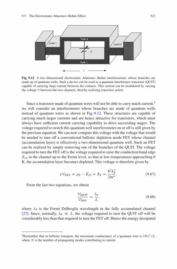
9.5 The Electrostatic Aharonov–Bohm Effect 523
L
V
Path 1
Path 2
Lead 2Lead 1
Fig. 9.12 A two dimensional electrostatic Aharonov–Bohm interferometer whose branches aremade up of quantum wells. Such a device can be used as a quantum interference transistor (QUIT)capable of carrying large current between the contacts. This current can be modulated by varyingthe voltage V between the two channels, thereby realizing transistor action
Since a transistor made of quantum wires will not be able to carry much current,8
we will consider an interferometer whose branches are made of quantum wellsinstead of quantum wires as shown in Fig. 9.12. These structures are capable ofcarrying much larger currents and are hence attractive for transistors, which mustalways have sufficient current carrying capability to drive succeeding stages. Thevoltage required to switch this quantum well interferometer on or off is still given bythe previous equation. We can now compare this voltage with the voltage that wouldbe needed to turn off a conventional ballistic depletion mode FET whose channel(accumulation layer) is effectively a two-dimensional quantum well. Such an FETcan be realized by simply removing one of the branches of the QUIT. The voltagerequired to turn the FET off is the voltage required to raise the conduction band edgeEc0 in the channel up to the Fermi level, so that at low temperatures approaching 0K, the accumulation layer becomes depleted. This voltage is therefore given by
eVjFET D �F �Ec0 D EF D „2k2F2m� : (9.67)
From the last two equations, we obtain
VjQUIT
VjFETD �F
L; (9.68)
where �F is the Fermi DeBroglie wavelength in the fully accumulated channel[27]. Since, normally, �F � L, the voltage required to turn the QUIT off will beconsiderably less than that required to turn the FET off. Hence the energy dissipated
8Remember that in ballistic transport, the maximum conductance of a quantum wire is 2Ne2=h,where N is the number of propagating modes contributing to current.

524 9 Quantum Devices and Mesoscopic Phenomena
in turning the QUIT on or off will be much less than the energy dissipated in turningthe FET on or off. This is the major advantage of quantum interference transistors,namely that they can be very energy efficient. In spite of that, QUIT-type devicesnever made any headway because they are extremely difficult to operate in practice.An electron’s phase is a delicate entity and preserving that throughout the deviceis a very tall order at any finite temperature. At the time of this writing, nobodyhas been able to demonstrate any QUIT type of transistor convincingly, althoughmodulation of the conductance of a ring by a potential applied to one arm has beendemonstrated [28].
9.5.1 The Effect of Multiple Reflections
In the foregoing discussions about AB interferometers or rings, we had alwaysneglected multiple reflection effects. We can now account for those by usingscattering matrices. For this purpose, refer to Fig. 9.13.
At either lead of the ring, we have a three way splitter and we can write thescattering matrices for these junctions as
2
4
A�BC1
BC2
3
5 D2
4
�.aC b/�p��� �p
���
p� a bp� b� a
3
5
2
4
ACB�1
B�2
3
5 (9.69)
and2
4
DCC�1
C�2
3
5 D
2
64
�.a0 C b0/�p
�0�� �p
�0��
p�0 a0 b0p�0 b0�a0
3
75
2
4
D�CC1
CC2
3
5 ; (9.70)
at the left and right leads, respectively. Here we have used the property that thescattering matrix is symmetric in the absence of any magnetic field. Of course, inthe case of the magnetostatic effect, a magnetic field will be present, but we willassume that it is enclosed entirely within the branches of the ring and does not enterthe leads, or even the branches for that matter.
The scattering matrix describing propagation through the two branches of thering is
2
664
B1�B�2
CC1
CC2
3
775
D
2
664
r1 0 t01 0
0 r2 0 t02
t1 0 r01 0
0 t2 0 r02
3
775
2
664
BC1
BC2
C�1
C�2
3
775; (9.71)
where tn and rn are the transmission and reflection amplitudes in the n-th branch.The unprimed and primed quantities are associated with propagation from left to

9.5 The Electrostatic Aharonov–Bohm Effect 525
A
A
+
-
B1+
B1-
B2+
B-2-
C1+
C1-
C2+
C2-
D
D
+
-
A B C D
τ P
a
b τ’
ρ
ρ’P’
P
τ’Pτ
Pτ
τ’τ’PρP’ρ’Pτ
ρ
ρ’P’
P
τ
τ’
ρ’
ρ
P
P’
P τ’PρP’ρ’PρP’ρ’Pτ
+
+
+
...
Fig. 9.13 (a) The incoming and outgoing waves at the leads and within the branches of a ringacting as either a magnetostatic or an electrostatic Aharonov–Bohm interferometer; (b) the multiplereflection trajectories within the ring
right and right to left, respectively. If transport is ballistic, then r1 D r2 D r 01 D
r 02 D 0 and in the absence of any magnetic or electric field inducing the AB effect,t1 D t 01 D Ot1 D exp.ik1L1/ while t2 D t 02 D Ot2 D exp.ik2L2/. Here,Ln is the lengthof the n-th branch in the direction of current flow.
When a static magnetic flux is present to induce the magnetostatic AB effect, thetransmission amplitudes transform as follows:
t1 ! Ot1ei�1 t 01 ! Ot1e�i�1
t2 ! Ot2ei�2 t 02 ! Ot2e�i�2; (9.72)
where �1 D R L10
EA � dEl1 and �2 D R L20
EA � dEl2, and the line integrals are taken alongthe two branches.

526 9 Quantum Devices and Mesoscopic Phenomena
Similarly, when an electrostatic potential is imposed between the two branches toinduce the electrostatic AB effect, the transmission amplitudes transform as follows:
t1 ! Ot1 t 01 ! Ot1t2 ! Ot2ei� t 02 ! Ot2ei� ; (9.73)
where � is the additional phase shift between the two paths caused by the appliedpotential inducing the electrostatic AB effect.
For mathematical convenience, we can write (9.69) as�
A�BC
�
D��.aC b/ �
� �
� �
ACB�
�
; (9.74)
where BC is a 2 � 1 column matrix whose elements are BC1 and BC
2 , B� is a 2 � 1column matrix whose elements are B�
1 and B�2 , � is a 2 � 1 column matrix whose
elements arep� and � is its hermitian conjugate, which is a 1 � 2 row matrix whose
elements are�p���
. Finally, � is a 2 � 2 matrix given by the lower right 2 � 2 blockof the 3 � 3 matrix in (9.69).
Similarly, we can reduce (9.70) to�DCC�
�
D��.a0 C b0/ � 0
� 0 �0� �
D�CC
�
; (9.75)
where � 0 is a 2 � 1 column matrix whose elements arep�0 and �0 is a 2 � 2 matrix
given by lower right 2�2 block of the 3 � 3 matrix in (9.70).Finally, the scattering matrix describing ballistic propagation through the
branches can also be reduced to a 2 � 2 matrix as
�B�CC
�
D�0 P 0P 0
� �BCC�
�
; (9.76)
where
P D�
t1 0
0 t2
�
(9.77)
and
P 0 D�t 01 00 t 02
�
(9.78)
Using a bit of algebra, we can now relate DC to AC and write the transmissionamplitude associated with traversing the ring as [29]
t D DC
AC D � 0ŒI � P�P 0�0��1P �
D � 0 �I C P�P 0�0 C .P�P 0�0/2 C .P�P 0�0/3 C : : :�
P�; (9.79)
where I is the 2 � 2 identity matrix.

9.5 The Electrostatic Aharonov–Bohm Effect 527
The last expression makes perfect sense since we can draw the Feynman pathsassociated with multiple reflection trajectories within the ring and sum the infinitegeometric series made up of these paths as shown in Fig. 9.13b. This will yield theexpression in the previous equation.
If there is a single propagating mode in each arm of the ring, then substitutingfor � , � 0, �, �0, P , and P 0 in last expression, we get
t D �Œ.t1 C t2/� .b � a/2t1t2.t 01 C t 02/�Œ1 � t1.a2t
01 C b2t 02/�Œ1 � t2.a2t
02 C b2t 01/� � a2b2t1t2.t
01 C t 02/2
; (9.80)
where, for simplicity, we have assumed that a, b, and � are all real, while a D a0,b D b0, and � D �0. The last three equalities apply only if the junctions at the leftand right lead are identical.
If a magnetic field is present, then we can use (9.72) to rewrite the last equation as
t .�1; �2/
D ��� Ot1ei�1 C Ot2ei�2
�� .b � a/2 Ot1 Ot2 � Ot1ei�2 C Ot2ei�1��
�
1� Ot1 �a2 Ot1 C b2 Ot2ei.�1��2/�� �
1� Ot2 �a2 Ot2 C b2 Ot1e�i.�1��2/��� a2b2 Ot1 Ot2 � Ot1ei.�1��2/=2 C Ot2e.�2��1/=2
�2;
(9.81)
Next, we will assume a perfectly symmetric interferometer with identicalbranches so that the quantities with carets are equal, i.e., Ot1 D Ot2. This simplifiesthe last equation to
t Œ.˚/� D� Ot1ei�1
�
1C ei.�2��1/� h
1� .b � a/2 Ot12i
h
1� Ot12�
a2 C b2ei.�1��2/�i h
1� Ot12�
a2 C b2ei.�2��1/�i� a2b2 Ot14
�
ei.�2��1/=2 C e�i.�2��1/=2�2
D� Ot1ei�1
�
1C ei.�2��1/� h
1� .b � a/2 Ot12i
h
1� Ot12�
a2 C b2ei.�1��2/�i h
1� Ot12�
a2 C b2ei.�2��1/�i� 4a2b2 Ot14 cos2
��2��12
�
D� Ot1ei�1
�
1C ei.˚/� h
1� .b � a/2 Ot12i
h
1� Ot12 .a2 C b2e�i.˚//i h
1� Ot12 .a2 C b2ei.˚//i
� 4a2b2 Ot14 cos2 Œ.˚/=2�; (9.82)
where.˚/ D �2 � �1 is the magnetostatic AB phase shift.The above expression shows that the transmission through the ideal symmetric
ring vanishes in ballistic transport whenever .˚/ D .e=„/˚ D .2n C 1/� , orequivalently when ˚ D .nC 1=2/.h=e/, where n is an integer. This is of course thebasis of magnetostatic AB conductance oscillations. But surprisingly, it also showsthat the conductance of the ring vanishes when
.b � a/2 Ot12 D 1: (9.83)
Using the unitarity of the scattering matrix, it is easy to show that b � a D 1, sothat the last equation becomes
Ot12 D e2ikL D 1; (9.84)

528 9 Quantum Devices and Mesoscopic Phenomena
or
kL D m�; (9.85)
wherem is an integer. Thus, the conductance of the ring should vanish, regardless ofthe magnetic flux threading it, whenever the last equation is satisfied. This conditionimplies that if the phase shift of an electron, traveling once full-circle around thering, is an even multiple of � , then the ring will not conduct at all. This happensbecause the electron enters the ring from the left lead into one arm, is reflected atthe right lead into the other arm, and arrives at the left lead with a phase shift of2m� and hence interferes with itself constructively. This maximizes the reflectionand minimizes the transmission, making the latter zero. We will call this conditionFabry–Perot resonance since that is associated with a round-trip phase shift of 2m� .When the ring is Fabry–Perot resonant, nothing conducts through it and it becomesan “insulator” no matter what its constituent material is.
However, there is a caveat. If (9.83) is satisfied, then the denominator of theexpression for transmission in (9.82) can be written as
denominator D �
1 � .a2 C b2e�i.˚//� �
1 � .a2 C b2ei.˚//�
� 4a2b2 cos2 Œ.˚/=2� : (9.86)
It is easy to verify that this denominator vanishes whenever .˚/ D .e=„/˚ D2n� , or when ˚ D n.h=e/. Since the numerator is also zero because of Fabry–Perot resonance, we have the situation that the transmission assumes the form of0/0 whenever ˚ D n.h=e/. Application of L’Hospital’s rule, however, shows thatthe transmission becomes unity at these values of the flux. Thus, the conductanceof a Fabry–Perot resonant ring will be zero at all values of the flux except whenit is n.h=e/. Only at those critical values, the ring will conduct. Therefore, a plotof the conductance versus magnetic flux of a Fabry–Perot resonant ring fulfillingthe condition in (9.83) will be a series of spikes at flux values of n.h=e/. At finitetemperatures, these spikes will have a finite width.
In the case of the electrostatic AB effect, the transformations in (9.73) will reduce(9.80) for the transmission amplitude to
t.�/ D t Œ0.E;V/�
D� Ot1�
1C ei0.E;V/� h
1� .b � a/2 Ot12ei0.E;V/i
h
1� Ot12 .a2 C b2ei0 .E;V//i h
1� Ot12 .a2ei20.E;V/ C b2ei0.E;V//i
� 4a2b2 Ot14ei20.E;V/cos2 Œ0.E;V/�:
(9.87)
The numerator in this expression vanishes (but the denominator does not vanish)whenever0.E;V/ D .2nC 1/� , which corresponds to destructive interference ofwaves traversing the two arms. If this condition is met, the transmission through thering will plummet to zero, and we will get a set of conductance minima which weshall call the primary minima. They are associated with the normal electrostatic ABeffect.

9.5 The Electrostatic Aharonov–Bohm Effect 529
Note, however, that the numerator also vanishes whenever0.E;V/ is such that
.b � a/2 Ot12ei0.E;V/ D ei.2kLC0.E;V// D 1; (9.88)
or
2kLC0.E;V/ D 2m�: (9.89)
When this condition is fulfilled, the numerator vanishes all right, but what about thedenominator? The latter will also vanish if 0.E;V/ D 2n� , in which case we willonce again end up with a 0/0 form. Combining the two conditions, we find that the0/0 situation arises if 2kL D 2.m�n/� , or if the phase shift going full circle aroundthe ring in the absence of any external field is an even multiple of � . Such a ring isof course Fabry–Perot resonant and does not conduct in the absence of any magneticor electric field. But if the ring is not Fabry–Perot resonant, then the 0/0 form doesnot arise (since the denominator does not vanish) and the transmission through thering will reach zero whenever (9.89) is fulfilled. We call the corresponding set ofconductance minima the secondary minima. Note that (9.89) corresponds to thesituation that under the applied potential V, the phase shift going full circle aroundthe ring is an even multiple of � , i.e., the ring becomes Fabry–Perot resonant onlywhen the correct potential obeying (9.89) is applied between the two arms. Notealso that the phase shift going full circle is an even multiple of � whether we travelclockwise or counterclockwise. In other words, each time-reversed path going fullcircle around the ring interferes constructively with itself. Not only do they interfereconstructively with each other, but each interferes constructively with itself. Wecan call this phenomenon voltage-induced Fabry–Perot resonance and this is whatcauses the secondary minima. The existence of this effect was first pointed outin [30].
It is natural to ask if there is a counterpart in the magnetostatic effect, namelyflux-induced Fabry–Perot resonance in a ring. In this case, the correspondingcondition would have been
2kLC.˚/ D 2m� (9.90)
for one time-reversed path, and
2kL �.˚/ D 2p� (9.91)
for the other, since the magnetic AB phase has opposite signs for clockwiseand counterclockwise travel. This shows that the following conditions have to befulfilled if each time-reversed path interferes constructively with itself:
2kL D .mC p/�
.˚/ D .m � p/�; (9.92)
wherem and p are integers.

530 9 Quantum Devices and Mesoscopic Phenomena
Two situations now arise. First, ifm�p is even, then fulfillment of the conditionsin (9.92) makes both the numerator and the denominator of the transmissionamplitude in (9.82) vanish, resulting in a 0/0 form. We already saw this situationand found that L’Hospital’s rule makes the transmission tend to unity and not zero.Hence, we do not get a secondary conductance minimum ifm�p is even. However,ifm�p is odd, then the numerator vanishes but the denominator does not, so that wedo get a set of secondary minima when .˚/ D .2l C 1/� [l = an integer]. It thustranspires that the conditions for the occurrence of the primary set of minima andthe secondary set of minima are identical, i.e., they both occur at exactly the samevalue of the flux˚ D .lC1=2/.h=e/. Hence the two sets are indistinguishable fromeach other in the case of the magnetostatic effect.
Let us now investigate if they are indistinguishable from each other in the caseof the electrostatic effect as well. For that to happen, we will need
0.E;V/primary �0.E;V/secondary D .2nC 1/� � .2m� � 2kL/ D 2l�; (9.93)
which translates to
2kL D Œ2.l Cm � n/ � 1�� D .2j C 1/�; (9.94)
where j D l C m � n � 1. Thus, the primary and secondary minima becomeindistinguishable only if the round-trip phase shift around the ring is an odd multipleof � in the absence of any electric or magnetic field, i.e., the ring is anti-Fabry–Perotresonant. In the end, we will observe two distinct sets of conductance minima in theelectrostatic effect, unless the ring is either Fabry–Perot resonant (in which case thesecondary minima do not occur) or Fabry–Perot anti-resonant (in which case theprimary and secondary minima overlap). The purpose of this entire exercise was toshow that multiple reflections can have nontrivial effects. They can cause secondaryconductance minima in electrostatic AB modulation, make the transmission go tounity in DBRTDs, etc. Thus, it is always important to account for their role.
9.6 Mesoscopic Phenomena: Applications of Buttiker’sMultiprobe Formula
Any solid-state device or structure can exhibit unusual and unexpected features atlow temperatures when the phase breaking length of charge carriers becomes longerthan the physical dimensions of the device. Charge transport in these devices isphase-coherent and can be described by the Landauer–Buttiker formalism as longas linear response conditions hold. Such devices have been termed “mesoscopicdevices” since their dimensions are between the macroscopic and the microscopic(typically few tens to few hundreds of nanometers). We will conclude this chapterwith some examples of unusual phenomena observed in the electrical resistance
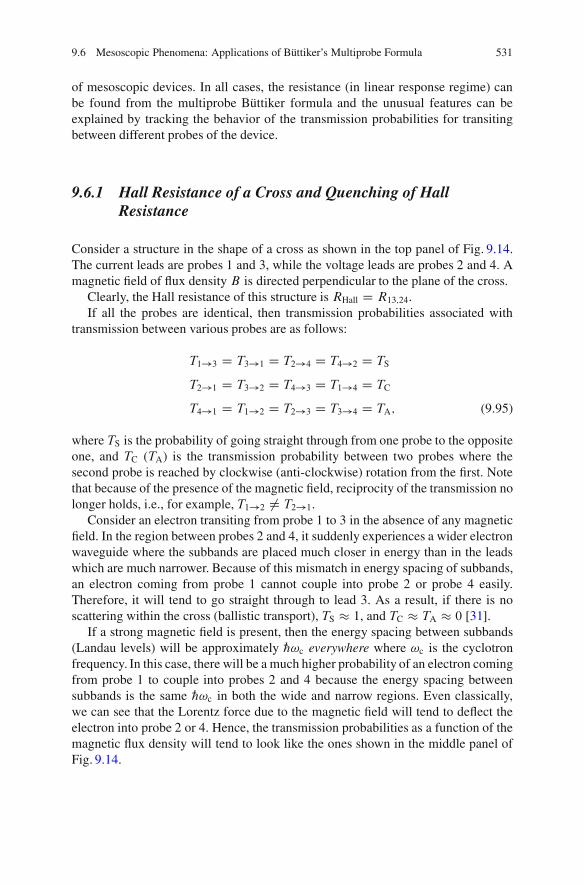
9.6 Mesoscopic Phenomena: Applications of Buttiker’s Multiprobe Formula 531
of mesoscopic devices. In all cases, the resistance (in linear response regime) canbe found from the multiprobe Buttiker formula and the unusual features can beexplained by tracking the behavior of the transmission probabilities for transitingbetween different probes of the device.
9.6.1 Hall Resistance of a Cross and Quenching of HallResistance
Consider a structure in the shape of a cross as shown in the top panel of Fig. 9.14.The current leads are probes 1 and 3, while the voltage leads are probes 2 and 4. Amagnetic field of flux density B is directed perpendicular to the plane of the cross.
Clearly, the Hall resistance of this structure is RHall D R13;24.If all the probes are identical, then transmission probabilities associated with
transmission between various probes are as follows:
T1!3 D T3!1 D T2!4 D T4!2 D TS
T2!1 D T3!2 D T4!3 D T1!4 D TC
T4!1 D T1!2 D T2!3 D T3!4 D TA; (9.95)
where TS is the probability of going straight through from one probe to the oppositeone, and TC (TA) is the transmission probability between two probes where thesecond probe is reached by clockwise (anti-clockwise) rotation from the first. Notethat because of the presence of the magnetic field, reciprocity of the transmission nolonger holds, i.e., for example, T1!2 ¤ T2!1.
Consider an electron transiting from probe 1 to 3 in the absence of any magneticfield. In the region between probes 2 and 4, it suddenly experiences a wider electronwaveguide where the subbands are placed much closer in energy than in the leadswhich are much narrower. Because of this mismatch in energy spacing of subbands,an electron coming from probe 1 cannot couple into probe 2 or probe 4 easily.Therefore, it will tend to go straight through to lead 3. As a result, if there is noscattering within the cross (ballistic transport), TS � 1, and TC � TA � 0 [31].
If a strong magnetic field is present, then the energy spacing between subbands(Landau levels) will be approximately „!c everywhere where !c is the cyclotronfrequency. In this case, there will be a much higher probability of an electron comingfrom probe 1 to couple into probes 2 and 4 because the energy spacing betweensubbands is the same „!c in both the wide and narrow regions. Even classically,we can see that the Lorentz force due to the magnetic field will tend to deflect theelectron into probe 2 or 4. Hence, the transmission probabilities as a function of themagnetic flux density will tend to look like the ones shown in the middle panel ofFig. 9.14.

532 9 Quantum Devices and Mesoscopic Phenomena
1
2
3
4
TC
TATs
B
TsTA TC
B
B B
B
R = RHall 13,24
Fig. 9.14 (Top panel). A Hall bar in the shape of a cross, with four terminals. Transmissionprobabilities between two probes where the ending probe is found by rotating clockwise or anti-clockwise from the starting probe are shown. (Middle panel) The magnetic field dependence of thetransmission probabilities between the probes. (Bottom panel) The magnetic field dependence ofthe Hall resistance showing the quenching

9.6 Mesoscopic Phenomena: Applications of Buttiker’s Multiprobe Formula 533
We will now calculate the 4-terminal Hall resistance RHall D R13;24.Using (8.164), we can write
2
6664
I1
I2
I3
I4
3
7775
D 2e
h
2
6664
P
j;j¤1 T1!j �T2!1 �T3!1 �T4!1
�T1!2
P
j;j¤2 T2!j �T3!2 �T4!2
�T1!3 �T2!3
P
j;j¤3 T3!j �T4!3
�T1!4 �T2!4 �T3!4
P
j;j¤4 T4!j
3
7775
2
6664
�1
�2
�3
�4
3
7775;
(9.96)
Using (9.95), we can write the previous equation as
2
664
I1I2I3
I4
3
775
D 2e
h
2
664
T �TC �TS �TA
�TA T �TC �TS
�TS �TA T �TC
�TC �TS �TA T
3
775
2
664
�1�2�3
�4
3
775; (9.97)
where T D TS CTA CTC. Note that every column and every row of the 4 � 4 matrixadds up to zero.
In the Hall measurement set up, we will pass current between probes 1 and 4,while connecting an ideal voltmeter of infinite resistance between terminals 2 and 3to measure the Hall voltage. Since there will be no current flowing out of the latterprobes, we will set I2 D I4 D 0. Similarly I1 D �I3 D I . Therefore, we get fromthe preceding equation
�TA�1 C T�2 � TC�3 � TS�4 D 0 Œfrom I2 D 0�
�TC�1 � TS�2 � TA�3 C T�4 D 0 Œfrom I4 D 0�
I D 2e
hŒT�1 � TC�2 � TS�3 � TA�4� D 2e
hŒTS�1 C TA�2 � T�3 C TC�4�:
(9.98)
From (9.98) we get
�1 D T�2 � TC�3 � TS�4
TAD T
TA�2 � TC
TA�3 � TS
TA�4
�3 D T�4 � TC�1 � TS�2
TAD T
TA�4 � TC
TA�1 � TS
TA�2: (9.99)
Substituting the expression for �3 in the relation for �1, we get
�1 D T TA C TCTS
T 2A � T 2C�2 � T TC C TSTA
T 2A � T 2C�4: (9.100)

534 9 Quantum Devices and Mesoscopic Phenomena
Putting the last result in the expression for �3 in (9.99), we obtain
�3 D T TA C TCTS
T 2A � T 2C�4 � T TC C TSTA
T 2A � T 2C�2: (9.101)
Substituting the last two relations in (9.98) and regrouping terms, we get
�T 2TA C T TCTS
T 2A � T 2C� TC C T TCTS C T 2S TA
T 2A � T 2C
�
�2 ��T 2TC C T TSTA
T 2A � T 2CC TA C T TATS C TCT
2A
T 2A � T 2C
�
�4
D�T 2TA C T TCTS
T 2A � T 2C� TC C T TCTS C T 2S TA
T 2A � T 2C
�
�4 ��T 2TC C T TSTA
T 2A � T 2CC TA C T TATS C TCT
2A
T 2A � T 2C
�
�2:
(9.102)
which yields�2 D ��4: (9.103)
Substituting the last result in (9.100) and (9.101), we find
�1 D ��3: (9.104)
Using the previous relations to write �1, �3, and �4 in terms of �2 in (9.98),we get
I D 2e
hŒ.T C TS/�1 C .TA � TC/�2�: (9.105)
Finally, using (9.100) to write �1 in terms of �2, we obtain
I D 2e
h
2ŒT 2A C T 2C C 2TS.TA C TC C TS/�
TA � TC�2: (9.106)
The Hall resistance is given by
RHall D R13;24 D �2 � �4
eID 2�2
eID h
2e2TA � TC
T 2A C T 2C C 2TS.TA C TC C TS/:
(9.107)
Using the magnetic-field dependence of TS, TA, and TC shown in the middlepanel of Fig. 9.14, we can see from the last expression for the Hall resistancethat the latter will have (qualitatively) a magnetic-field dependence as shown inthe bottom panel of Fig. 9.14. There will be a dead zone straddling the origin atB D 0 because TA D TC D 0 near B D 0. This is called “quenching of the Hallresistance.” Normally, the Hall resistance should increase linearly with the B-field(recall Chap. 1 discussion), but in phase coherent transport in a mesoscopic Hall bar,one can see the quenching. This has been experimentally observed and discussed bymany authors [32, 33].

9.6 Mesoscopic Phenomena: Applications of Buttiker’s Multiprobe Formula 535
B
Rbend = R12,34Fig. 9.15 The magnetic fielddependence of the bendresistance
9.6.2 Bend Resistance of a Cross
We can define a “bend resistance” of the same cross as the resistance measuredby passing current between probes 1 and 2, while measuring the voltage betweenprobes and 4, i.e.,
Rbend D R12;34 D �3 � �4eI 0 ; (9.108)
where I 0 is the current flowing between terminals 1 and 2.It can be shown in the manner of the preceding analysis (see Problem 9.6), that
the bend resistance is given by the expression
Rbend D R12;34 D h
2e2T 2S � TCTA
T�
T 2A C T 2C�C TS
�
T 2 � T 2S�C 2TCTATS
: (9.109)
Once again, using the magnetic field dependence of the transmission probabilitiesshown in the middle panel of Fig. 9.14, we see that the bend resistance should havea qualitativeB-field dependence as shown in Fig. 9.15. Such a dependence has beenobserved experimentally [34].
9.6.3 An Alternate Explanation of the Integer QuantumHall Effect
We had mentioned in Chap. 7 that Laughlin’s explanation for the integer quantumHall effect invokes phase coherence of the electron’s wavefunction in the entiresample. Real samples, however, are much larger than the phase coherence lengthof charge carriers so that Laughlin’s explanation cannot apply to them. In 1988,Buttiker advanced an alternate explanation for the integer quantum Hall effect thatdoes not require global phase coherence of the electron’s wavefunction [35]. All thatit requires are two conditions:
1. At very high magnetic fields, electrons in the center of the sample executecyclotron motion in closed orbits which have no resultant velocity and hence

536 9 Quantum Devices and Mesoscopic Phenomena
Contact 1 Contact 2
Edge states
Closed cyclotronorbit
Fig. 9.16 Only edge states located at opposite edges of a sample carry current in oppositedirections under high magnetic fields. States in the interior of the sample execute cyclotron motionin closed orbits. They have no resultant translational velocity and hence carry no current
carry no current. Current is carried only by states that are localized at the edges ofthe sample (edge states). This is a consequence of the dispersion relations shownin Fig. 7.13. The velocity of the electron in any magnetoelectric subband n isgiven by vx D @En
@kxD @En
@y0
@y0@kx
. We can view the dispersion relation in Fig. 7.13 asa plot of energy versus y0 for a fixed kx . This shows that the dispersion relationswill have a nonzero slope only at the edges of the sample at high magnetic fields,so that only edge states will have a nonzero velocity and carry current. Thiswas shown explicitly by Halperin [36]. Furthermore, the slopes of the dispersionrelations have opposite signs at opposite edges of the sample, which means thatedge states at one edge carry current in one direction and those at the other edgecarry current in the opposite direction. This is depicted in Fig. 9.16.
2. Backscattering is suppressed at high magnetic fields. Since edge states located atopposite edges of the sample carry current in opposite directions, backscatteringwill require scattering of an electron from one edge to the other, which requiressignificant overlap between wavefunctions located at opposite edges. However,at strong magnetic fields, this overlap is very small as seen in Fig. 7.14. Hence,the possibility of backscattering due to either elastic or inelastic scattering isvanishingly small. We had already discussed this in Chap. 7. Forward scatteringis, however, very much permitted. An electron can scatter from one edgestate into another located at the same edge since the overlap between theirwavefunctions is large.
Buttiker provided a physical explanation of how an elastic scatterer like animpurity cannot cause backscattering. He invoked the classical skipping orbitpicture of edge states that we discussed in Chap. 7. If a skipping orbit hits animpurity, as shown in Fig. 9.17, it turns around, bends back in a cyclotron orbit,strikes the impurity again, and is scattered forward. If we consider a box surroundingthis impurity and if its dimension is larger than the diameter of the cyclotron orbit,then every electron entering this box in one of the edge states will leave this box

9.6 Mesoscopic Phenomena: Applications of Buttiker’s Multiprobe Formula 537
Elasticscatterer
Sample edge
Cyclotron orbit
Skippingorbit
Fig. 9.17 A physical picture to explain why an elastic scatterer like an impurity cannot causebackscattering under high magnetic fields. The electron trajectory is reflected by the impurity, butit turns around due to cyclotron motion and ultimately is always scattered it forward. Adapted withpermission from [35]. Copyrighted by the American Physical Society
traveling forward in the same or another of the edge states located at the sameedge. There is no reversal of motion over distances large compared to the cyclotrondiameter. Hence, backscattering is suppressed as long as the mean distance betweenimpurities is considerably larger than the cyclotron radius. Of course, this meansthat in order to suppress backscattering in a more disordered sample having a largerimpurity density, a higher magnetic field will be needed.
Since electrons entering the sample in the edge state i must always leave thesample in an edge state j located at the same edge when the magnetic field is high,it is obvious that the transmission probability from one edge state to another at thesame edge must obey the relation
X
j
Tij .˙B/ D 1; (9.110)
where Tij is the probability of transmitting from edge state i to edge state j and Bis the magnetic flux density. By invoking reciprocity, i.e., Tj i .B/ D Tij .�B/, wefind that
Ti DX
j
Tj i .B/ D 1; (9.111)
which means that the transmission probability from all edge states localized at oneedge into any given edge state i localized at the same edge must add up to unity.
The same is true of edge states located at the opposite edge of the samples.Denoting their transmission probabilities with a prime, we obtain
T 0i D
X
j
T 0j i .B/ D 1; (9.112)

538 9 Quantum Devices and Mesoscopic Phenomena
As a consequence of this property, namely that the transmission probability ofevery edge state Ti is unity at high magnetic fields, the 2-probe Landauer resistanceof the device shown in Fig. 9.16 will be quantized and given by
R2-probe D h
e21
N; (9.113)
where N is the number of occupied spin–split edge states. On the other hand, whenthe magnetic field is low and backscattering is not suppressed, the 2-probe Landauerresistance will not be quantized and will be given by
R2-probe D h
e21
T; (9.114)
where T can take any value between 0 and N .Now, the manifestation of the integer quantum Hall effect is the vanishing of
the longitudinal resistance Rxx and the quantization of the Hall resistance Ryx athigh magnetic fields, where the Ex is the direction of current flow. Buttiker showedhow these two features will come about in a sample at high magnetic fields, even inthe presence of inelastic scattering which destroys phase coherence of the electronwavefunction. He did this by treating inelastic scattering as lumped contacts withdifferent chemical potentials distributed throughout the sample. This proof is quiteinvolved and omitted here, but can be found in [35]. Instead, we will consider onlythe case of a phase coherent sample and show that Rxx vanishes and Ryx indeedbecomes quantized to .1=p/.h=e2/ [p D integer]. We do this by using the Buttikermultiprobe formula and make use of (9.111) and (9.112).
In Fig. 9.18, we show the usual 6-terminal Hall bar sample. Note that only edgestates carry current and they are shown. Clearly, using (9.111) and (9.112), we get
T1!2 D T2!3 D T3!4 D T4!5 D T5!6 D T6!1 D M; (9.115)
whereM is the number of occupied spin–split edge states. All other Ti!j vanish.Using Buttiker’s multiprobe formula given in (8.164), we obtain the following
relations between the currents and the chemical potentials in the six terminals:
2
66666664
I1
I2I3I4I5
I6
3
77777775
D e
h
2
66666664
M 0 0 0 0 �M�M M 0 0 0 0
0 �M M 0 0 0
0 0 �M M 0 0
0 0 0 �M M 0
0 0 0 0 �M M
3
77777775
2
66666664
�1
�2�3�4�5
�6
3
77777775
(9.116)
Note that here we have used e=h instead of 2e=h since the edge states are assumedto be spin–split.

9.6 Mesoscopic Phenomena: Applications of Buttiker’s Multiprobe Formula 539
1
2 3
4
56
Voltmeter
Current source
Hall voltmeter
Fig. 9.18 A Hall bar with 6 terminals. All current carrying states are shown
Since we will be measuring the longitudinal resistance by injecting current intoprobe 1, extracting it from probe 4, and connecting a voltmeter across probes2 and 3, there will be no current flowing in probes 2 and 3 since the voltmeterhas infinite resistance. Hence, I2 D I3 D 0, which immediately yields from thepreceding equation that �1 D �2 D �3. This means that the upper edge of thesample has become an equipotential surface and that it is maintained at the chemicalpotential of the left contact.
The longitudinal resistance Rxx will be
R14;23 D �2 � �3eI
D 0; (9.117)
where I D I1 D �I4.This shows that the longitudinal resistance indeed vanishes, which is one of the
manifestations of the integer quantum Hall effect.Now, in order to measure the Hall voltage, we will connect a Hall voltmeter
across leads 2 and 6. These leads will therefore draw no current so that I2 D I6 D 0.Using this in (9.116), we obtain �1 D �2 and �5 D �6.
Equation (9.116) also tells us that I D I1 D ehM.�1 � �6/. The Hall resistance
Ryx is by definition
R14;26 D �2 � �6eI
: (9.118)

540 9 Quantum Devices and Mesoscopic Phenomena
Using the two previously derived relation, we can rewrite the last equation as
R14;26 D h
e21
M
�1 � �6�1 � �6 D h
e21
M: (9.119)
This is the other manifestation of the integer quantum Hall effect, namely thatthe Hall resistance is quantized. Thus, the Buttiker multiprobe formula can providean elegant explanation for the integer quantum Hall effect in a phase coherent Hallbar! Of course, Buttiker extended this result to a phase-incoherent Hall bar as well,but that analysis is omitted here.
9.7 Summary
1. In quantum devices, or “mesoscopic devices,” where the electron’s wavefunctionremains coherent in the active region of the device, unusual effects can arise inthe current versus voltage characteristics, or the resistance of the device. Theseare often referred to as “mesoscopic phenomena.”
2. An example of a quantum device, where the electron wavefunction retainsphase coherence in the active device region, is the double-barrier-resonant-tunneling-diode which exhibits a nonlinear and nonmonotonic current versusvoltage characteristic, resulting in a region of negative differential resistance.This feature is due to resonant transmission through the device at certain electronenergies, which arises from multiple reflections of an electron wave between thebarriers. The current versus voltage relation can be obtained from the Tsu–Esakiformula and the transmission coefficient through the device can be calculated asa function of incident electron energy by solving the Schrodinger equation andthe Poisson equation self-consistently.
3. Another example of a quantum device is the stub-tuned transistor. The transmis-sion between two of the contacts—and hence the current flowing between thesetwo contacts—can be controlled with a voltage applied at the third terminal,thereby realizing transistor action. The transistor action is due to interferenceof multiply reflected waves whose relative phases are altered by the voltage atthe third terminal. This device is an electronic analog of the familiar microwavestub-tuned waveguide.
4. The AB effect demonstrates the importance of potentials in quantum mechanics.It shows that an electron that experiences the potential due an external agent, butnot the field associated with this potential, can still respond to the potential. Ina magnetic field, an electron acquires an AB phase due to the magnetic vectorpotential and this can manifest itself in interference effects. Such interferencecan be utilized to modulate the conductance of a ring by changing the magneticflux threading it, or by changing the potential difference between two arms ofa ring. The former results in magnetostatic conductance oscillations and thelatter in electrostatic conductance oscillations. In the former oscillations, the

Problems 541
conductance oscillates periodically with the magnetic flux with a period equalto the fundamental flux quantum h=e, whereas in the latter, the conductanceoscillates aperiodically with the potential difference between the two arms,thereby realizing transistor action. Such a transistor may be interesting becauseone might be able to switch it on or off with a very small voltage, therebydecreasing dynamic power dissipation that occurs during switching. However,such a transistor will also be very difficult to realize in practice since an electron’sphase is a very delicate entity and preserving it over an entire device is a tall order.
5. The AAS effect is related to the AB effect and arises from the interference of twotime-reversed paths of an electron, where one path goes clockwise and the othercounterclockwise around the annulus of a ring shaped conductor. This causes theconductance of a ring to oscillate periodically with the flux threading the ring,with a period that is one-half of the AB period, or h=2e.
6. In a mesoscopic device, whose dimensions are smaller than the phase coherencelength of charge carriers, unusual effects can be manifested in the resistance.Examples of this are the peculiar behavior of the Hall resistance and the bendresistance as a function of magnetic field. The Hall resistance deviates fromclassical behavior even at small magnetic fields when integer or FQHE doesnot arise. The Hall resistance can be zero around small magnetic fields, insteadof increasing linearly with magnetic field. This is termed quenching of Hallresistance. The bend resistance, on the other hand, can change sign as a functionof magnetic field. These effects can be explained by the dependence of thetransmission probabilities on magnetic field and the Buttiker multiprobe formularelating current and voltage in a multi-terminal device.
7. The Buttiker multiprobe formula can provide an elegant explanation of theinteger quantum Hall effect in the presence or absence of phase-randomizingscattering events, i.e. whether or not the device dimensions are larger than thephase coherence length of electrons. The only requirements are that the magneticfield be high enough that only edge states carry current and backscattering issuppressed.
Problems
Problem 9.1. Check if the scattering matrix of the DBRTD given by (9.4) and (9.5)is unitary.
Problem 9.2. Using (9.6), show that if the two barriers are not identical, then thetransmission amplitude through a DBRTD can be written as (9.18) provided thetransmission amplitude through each barrier is considerably less than unity. Thisproblem was studied by Ricco and Azbel (B. Ricco and M. Ya Azbel, “Physicsof resonant tunneling. The one-dimensional double barrier case,” Phys. Rev. B.,29, 1970 (1984)), who derived a relation for the resonant transmission amplitude

542 9 Quantum Devices and Mesoscopic Phenomena
through two unequal barriers. Their result disagrees with (9.20) by a factor of 2.Equation (9.18) has been derived somewhat differently in E. O. Kane, TunnelingPhenomena is Solids, Eds. E. Burstein and S. Lundqvist, (Plenum, New York, 1969).
Show that at resonance, the transmission through the two unequal barriers is lessthan or equal to unity.
Problem 9.3. Consider the set-up in Fig. 9.8. Assume that the magnetic vectorpotential EA in the paths of the electron is time invariant (but not necessarily spaceinvariant). Show that the phase difference between the wavefunctions sampling thetwo paths is indeed e
„H EA.Er/ � dEl , where the contour integral is the line integral of
the magnetic vector potential taken around the ring. Assume that the scalar potentialinside the ring does not vary in space and the two arms of the ring are identical.
Solution. The time-independent Schrodinger equation describing an electron in thering of Fig. 9.8 is (7.11). If we assume that the scalar potential inside the ring isspace invariant (and hence can be assumed to be zero), then (7.11) can be written as
"
�„2r2
2m� C ie„ Er � EA.Er/2m� C 2ie„ EA.Er/ � Er
2m� C ej EA.Er/j22m�
#
�.Er/ D E�.Er/;
where �.Er/ is the electron’s wavefunction anywhere within the ring.Since there is no magnetic field inside the ring, the electron’s energy should be
that of a free particle. Hence, the Schrodinger equation should become
"
�„2r2
2m� C ie„ Er � EA.Er/2m� C 2ie„ EA.Er/ � Er
2m� C ej EA.Er/j22m�
#
�.Er/ D „2k22m� �.Er/;
It is easy to show that the solution
�.Er/ D 1p˝
eiR �EkC e
„
EA.Er/�
�dEr:
satisfies the last equation and hence must be the wavefunction within the ring. Here˝ is a normalizing volume. This can be checked by substituting this solution in theprevious equation and noting that the equation reduces to an identity.
The electron is injected at the point of injection Er D Eri and then transmits intothe two paths. At the point of detection, which is at Er D Erd , the wavefunction of theelectron arriving from path 1 is
�1.Erd / D 1p˝
eiR
ErdEri
hEkC e„
EA.Er/i
�dEl1;
where the line integral is taken over path 1.
Problems 543
Similarly, the wavefunction of the electron in path 2 at the point of detection is
�2.Erd / D 1p˝
eiR
ErdEri
hEkC e„
EA.Er/i
�dEl2;
where the line integral is taken over path 2.The phase difference between �1.Erd / and �2.Erd / is:
� DZ Erd
Eri
hEk C e
„EA.Er/
i
� dEl1 �Z Erd
Eri
h Ek C e
„EA.Er/
i
� dEl2
DZ Erd
Eri
hEk C e
„EA.Er/
i
� dEl1 CZ Eri
Erd
hEk C e
„EA.Er/
i
� dEl2
D e
„I
EA.Er/ � dEl;
where we have used the fact thatR Erd
EriEk � dEl1 D R Erd
EriEk � dEl2 since the two paths are
identical.Note that using Stokes theorem, we can reduce the last equation to
� D e
„Z
s
Œ Er � EA.Er/� � d ES D e
„Z
s
EB � d ES D e
„˚;
where EB is the flux density and ˚ is the flux enclosed within the ring.
Problem 9.4. Show that the electrostatic AB phase shift can be written as
.E;V/ D e
„Vh�t.E/i;
where h�t.E/i is the average transit time of an electron of energy E (averaged overthe two branches of the interferometer) through the ring.
Problem 9.5. Equation (9.41) statesI
clockwise
Ek.Er/ � dEl DI
counter-clockwise
Ek.Er/ � dEl :
while (9.43) statesI
counter-clockwise
EA.Er/ � dEl D �I
clockwise
EA.Er/ � dEl :
How do you reconcile the fact that in one case there is no negative sign and inthe other case there is one? In other words, why are the contour integrals takenclockwise and counterclockwise equal in magnitude and of the same sign in onecase, and equal in magnitude but of opposite sign in the other case?Solution At any coordinate point in the ring, the electron’s wavevector Ek will pointin opposite directions during the clockwise and counterclockwise sojourns, which is

544 9 Quantum Devices and Mesoscopic Phenomena
Upper edge state
Lower edge state
magnetic field
Fig. 9.19 Edge states carrying current in an Aharonov–Bohm ring at very high magnetic fields.Note that the current carrying paths do not encircle a magnetic flux
why (9.41) is valid. However, at any coordinate point, the magnetic vector potentialEA will point in the same direction during the clockwise and counterclockwise
sojourns since the vector potential’s direction is determined by the magnetic fieldEB which is fixed. That is why (9.43) is also valid. This explains the presence of the
negative sign in one case and not in the other.
Problem 9.6. Derive the expression for the bend resistance of a cross given in(9.108). Hint: Ground terminal 4 so that �4 D 0 in order to simplify the algebra.
Problem 9.7. Consider a 4-probe conductor with probes k; l;m; n, where two ofthe probes are used to inject and extract current while the other two are used tomeasure voltage. Using (8.43), prove the reciprocity relation
Rkl;mn. EB/ D Rmn;kl .� EB/:
where EB is a magnetic field.
Problem 9.8. The critical magnetic flux density Bcrit for transition from the low-to the high-field region in the Buttiker picture of the integer quantum Hall effect isgiven by the condition that the cyclotron radius will be equal to the mean distancebetween impurities �. Show that Bcrit D m h
e�2, where m is an integer. Find the
critical flux density when � is 10 nm, assuming m D 1.
Problem 9.9. Using the edge state picture, show that the magnetostatic Aharanov–Bohm conductance oscillations in a ring will vanish at sufficiently high magneticfields.Solution. The edge states carrying current in a ring at very high magnetic fieldsare shown in Fig. 9.19. The current paths do not enclose any magnetic flux. Hence,

References 545
there is no AB effect! Therefore, the resistance of the ring will be independent ofmagnetic field and will be given by (9.113), where N is the number of occupiedspin–split edge states.
References
1. S. M. Sze, Physics of Semiconductor Devices, 2nd. edition, (John Wiley & Sons, New York,1981).
2. L. L. Chang, L. Esaki and R. Tsu, “Resonant tunneling in semiconductor double barriers”,Appl. Phys. Lett., 24, 593 (1974).
3. A. C. Seabaugh, “9-state resonant tunneling diode memory”, IEEE Elec. Dev. Lett., 13, 479(1992).
4. W. H. Lee and P. Mazumder, “Color image processing with quantum dot structure on multi-peak resonant tunneling diode”, 2007 7th IEEE Conference on Nanotechnology, 1–3, 1169(2007).
5. T. C. L. G. Sollner, W. D. Goodhue, P. E. Tannenwald, C. D. Parker and D. D. Peck, “Resonanttunneling through quantum wells at frequencies up to 2.5 THz”, Appl. Phys. Lett., 43, 588(1983).
6. M. Cahay, M. McLennan, S. Datta and M. Lundstrom, “Importance of space charge effects inresonant tunneling devices”, Appl. Phys. Lett., 50, 612 (1987).
7. T. Weil and B. Vinter, “Equivalence between resonant tunneling and sequential tunneling indouble barrier diodes”, Appl. Phys. Lett., 50, 1281 (1987).
8. M. Jonson and A. Grincwajg, “Effect of inelastic scattering on resonant and sequentialtunneling in double barrier heterostructures”, Appl. Phys. Lett., 51, 1729 (1987).
9. F. Capasso and R. A. Kiehl, “Resonant tunneling transistor with quantum well base and highenergy injection: A new negative differential resistance device”, J. Appl. Phys., 58, 1366(1985).
10. F. Capasso, S. Sen, F. Beltram and A. Y. Cho, “Resonant tunnelling and superlattice devices:Physics and circuits”, Chapter 7 in Physics of Quantum Electron Devices, Ed. F. Capasso,(Springer-Verlag, Berlin, 1990), p. 181.
11. R. F. Kazarinov and R. A. Suris, “Possibility of amplification of electromagnetic waves in asemiconductor with a superlattice”, Fiz. Tekh. Poluprov., 5, 797 (1971) [English translation:Sov. Phys. Semicond., 5, 707 (1971)].
12. R. F. Kazarinov and R. A. Suris, “Electric and electromagnetic properties of semiconductorswith a superlattice”, Fiz. Tekh. Poluprov., 6, 148 (1972) [English translation: Sov. Phys.Semicond., 6, 120 (1972)].
13. S. Luryi, “Frequency limit of double barrier resonant tunneling oscillators”, Appl. Phys. Lett.,47, 490 (1985).
14. L. A. MacColl, “Note on the transmission and reflection of wave packets by potential barriers”,Phys. Rev., 40, 621 (1932).
15. T. E. Hartman, “Tunneling of a wave packet”, J. Appl. Phys., 33, 3427 (1962).16. W. E. Hagstrom, “Quantum theory of tunneling”, Phys. Stat. Solidi. (b), 116, K85 (1983).17. J. R. Barker, “Quantum theory of hot electron tunneling in microstructures”, Physica BCC,
134, 22 (1985).18. M. Buttiker and R. Landauer, “Traversal time for tunneling”, Phys. Rev. Lett., 49, 1739 (1982);
IBM J. Res. Develop., 30, 451 (1986).19. S. Datta, “Quantum devices”, Superlat. Microstruct., 6, 83 (1989).20. F. Sols, M. Macucci, U. Ravaioli and K. Hess, “On the possibility of transistor action based in
quantum interference phenomena”, Appl. Phys. Lett., 54, 350 (1989).

546 9 Quantum Devices and Mesoscopic Phenomena
21. S. Subramaniam, S. Bandyopadhyay and W. Porod, “Analysis of the device performance ofquantum interference transistors utilizing ultrasmall semiconductor T structures”, J. Appl.Phys., 10, 347 (1991).
22. Y. Aharonov and D. Bohm, “Significance of electromagnetic potentials in the quantum theory”,Phys. Rev. 115, 485 (1959).
23. A. Tonomura, N. Osakabe, T. Matsuda, T. Kawasaki and J. Endo, “Evidence of Aharonov-Bohm effect with magentic field completely shielded from electron wave”, Phys. Rev. Lett.,56, 792 (1986).
24. B. L. Altshuler, A. G. Aronov and B. Z. Spivak, “The Aharonov-Bohm effect in disorderedconductors”, Pis’ma Zh. Eksp. Teor. Fiz., 33, 101 (1981) [English translation: JETP Lett., 33,94 (1981).]
25. B. Pannetier, J, Chaussy, R. Rammal and P. Gandit, “First observation of Altshuler-Aronov-Spivak effect in gold and copper”, Phys. Rev. B., 31, 3209 (1985).
26. S. Datta, M. R. Melloch, S. Bandyopadhyay and M. S. Lundstrom, Appl. Phys. Lett., 48, 487(1986).
27. S. Datta, “Quantum interference devices”, Chapter 10 in Physics of Quantum Electron Devices,Ed. F. Capasso, (Springer-Verlag, Berlin, 1990), p. 339.
28. P. G. N. de Vegvar, G. Timp, P. M. Mankiewich, R. Behringer and J. Cunningham, “TunableAharonov-Bohm effect in an electron interferometer”, Phys. Rev. B., 40, 3491 (1989).
29. P. W. Anderson, “New method for scaling theory of localization. II. Multichannel theory of a“wire” and possible extension to higher dimensionality”, Phys. Rev. B, 23, 4828 (1981).
30. M. Cahay, S. Bandyopadhyay and H. L. Grubin, “Two types of conductance minima inelectrostatic Aharonov-Bohm conductance oscillations”, Phys. Rev. B, 39, 12989 (1989).
31. H. U. Baranger and A. D. Stone, “Quenching of the Hall resistance in ballistic microstructures- a collimation effect”, Phys. Rev. Lett., 63, 414 (1989).
32. M. L. Roukes, A. Scherer, S. J. Allen Jr., H. G. Craighead, R. M. Ruthen, E. D. Beebe andJ. P. Harbison, “Quenching of the Hall effect in a one-dimensional wire”, Phys. Rev. Lett., 59,3011 (1987).
33. C. J. B. Ford, T. J. Thornton, R. Newbury, M. Pepper, H. Ahmed, D. C. Peacock, D. A. Ritchie,J. E. F. Frost and G. A. C. Jones, “Vanishing Hall voltage in a quasi one-dimensional GaAs-GaxAl1�xAs heterojunction”, Phys. Rev. B., 38, 8518 (1988).
34. Y. Takagaki, K. Gamo, S. Namba, S. Takaoka, K. Murase, S. Ishida, K. Ishibashi andY. Aoyagi, “Non local voltage fluctuations in a quasi ballistic electron waveguide”, Solid. St.Commun., 69, 811 (1989).
35. M. Buttiker, “Absence of backscattering in the quantum Hall effect in multiprobe conductors”,Phys. Rev. B., 38, 9375 (1988).
36. B. I. Halperin, “Quantized Hall conductance, current-carrying edge states, and the existence ofextended states in a two-dimensional disordered potential”, Phys. Rev. B., 25, 2185 (1982).

Index
AAbsorption, ix, 77, 80, 116, 149, 184, 209, 211,
216, 217, 220–222, 225–229, 232–234,237–242, 244–246, 248, 249, 251–253,257–259, 262–269, 277, 281, 288–290,298–300, 303, 306, 314–315, 320–321,328–334, 337, 339, 375–377, 388, 391
Aharonov–Bohm effect, 509–520, 540, 541,543
electrostatic, 520–530magnetostatic, 517–520, 522, 524, 525,
527, 529, 540, 544Altshuler–Aronov–Spivak effect, 512–516Auger recombination, 17, 19, 280
BBalance equation, vii, 41–45B-coefficient, 276Bend resistance, 535, 541, 544Bloch
function, 162, 166–168, 174, 175, 203, 213,219, 290, 297, 300, 302, 304, 306, 308,310, 334
theorem, 161, 165, 174, 184, 202, 204, 210,297, 302
Boltzmann distribution function, 25, 35–41,43, 50–60, 62, 65, 66, 71, 72f, 78, 79,81, 84, 88, 91, 187, 188, 459, 463, 466,467, 483
Boltzmann Transport equation, vii–ix, 25,30, 35–37–41, 58, 81, 82, 209, 250,459–464, 469, 479, 483
collisionless quantum, 459–464limitations, 39–40methods of solving, 58
Boltzmann transport model, 2, 4, 41, 209, 250,395, 400
Born approximation, 212, 254Bose–Einstein
condensate, 321, 322, 331distribution, 88factor, 221, 238, 267operators, 217, 218, 478statistics, 80, 271
Brillouin zone, 153, 154, 154f, 167–170,175–178, 181, 182, 191, 198f, 202, 203,206, 214, 261f, 263, 329, 331
Buttiker’s multi-probe formula, 448–451, 482,507, 530–540
CCancellation theorem, 159Cascading rule of
scattering matrices, 414–415transmission matrices, 122, 123, 407–409
Charge density operator, 99Chemical potential, viii, 54–58, 406, 435, 452,
473, 475, 482, 507, 521, 538, 539Closed system, 473, 476Collision retardation, 81Contact resistance, 455, 457, 483Core states, 156–158, 167Correlation energy, 398–400Correlation function, 462, 463, 466–470,
478–480, 483Correspondence principle, 92, 99, 100Crystal momentum, 6, 38Current density operator, 99, 100Cyclotron
frequency, 348, 392, 531
S. Bandyopadhyay, Physics of Nanostructured Solid State Devices,DOI 10.1007/978-1-4614-1141-3, © Springer Science+Business Media, LLC 2012
547

548 Index
Cyclotron (cont.)motion, 350, 351f, 359, 371, 387, 535,
536f, 537forbit, 348, 350–352, 357, 359, 360, 366,
370, 371, 373, 374, 386–388, 535, 536radius, 348, 369, 370, 537, 544
DDeBroglie
relation, 352wavelength, 93, 141, 264, 352, 398, 523wavevector, 93, 261
Deformation potential, 223Density matrix, 134, 466, 467, 505Density of states, viii, 25, 35, 64, 67, 70, 80,
83, 132, 133, 149, 184–203, 205, 230,233, 239, 242, 244, 246, 249, 254, 262,274, 288, 323, 331, 333, 336, 337, 339,342, 355–358, 356f, 363f, 387, 401,405, 436, 441, 487, 488
Density of states 1-D, 197Density of states 2-D, 190, 194, 196Density of states 3-D, 190, 195Density of states of phonons and photons,
197–202Dielectric confinement, 319–320, 330Diffusion coefficient, 12, 24–28, 35, 49, 51–58,
79, 81, 83, 397from carrier distribution function, 51–58from Monte Carlo simulation, 79
Dingle plot, 360Dirac equation, ix, 342, 344, 387
nonrelativistic approximation to, 343Drift–diffusion
equations, vii, 16, 22, 24, 36, 41, 45–50model, vii, 1–33, 43–89, 395, 400
Drift mobility, 7, 20, 21, 25Drude model, 5–11, 28, 67, 71
EEdge state, ix, 370–373, 388, 422, 484,
536–538, 541, 544, 545phenomena, 373–374
Ehrenfest theorem, 135Einstein relation, 25–26, 28, 30, 31, 49, 54, 83,
397Electron waveguide, 97–98, 138, 139, 506,
509, 517, 531Emission, ix, 1, 19, 77, 80, 116, 211, 216–217,
220–222, 226–228, 231, 233–237, 242,243, 248, 249, 252, 253, 257, 262, 263,265–279, 279f, 282, 283, 286, 288–290,
298–300, 303, 306, 314, 323–325,329–331, 334, 376, 388, 438, 487
spontaneous, ix, 220–222, 225–227, 236,253, 267, 268, 270–276, 281, 323, 324,329–331
stimulated, ix, 80, 116, 220, 221, 225–227,234, 236, 253, 266, 268–273, 277–279,325, 329
Equations of state, vii, 16, 28, 41Equipartition of energy, 225, 227, 229, 234Evanescent states, 124, 135, 138, 154, 286,
324, 326, 327, 331, 369, 404, 409, 411,412, 414, 415, 422, 428–432, 446, 482,498
Exchangeinteraction, 129, 318potential, 128, 129
Exciton, ix, 314–323, 330, 331, 334, 465Mott–Wannier type of-, 318
Extended zone representation, 154, 214
FFabry–Perot resonance, 570, 572, 577,
605–608Fermi’s Golden Rule, viii, ix, 52, 82, 116,
209–216, 219–229, 239, 250, 252, 254,266, 374, 395
Filling factor, 354, 378, 379, 386—-388Fock Darwin states, 390Free electron wavefunction, 94, 96–97, 151,
156, 202, 460
GGeneralized moment, vii, 41–45, 50, 81Generation, 15–19, 20, 27, 30, 46, 268, 314,
411Green’s function, ix, 470–473–479, 483
advanced, 472, 478, 483nonequilibrium, 478–480retarded, 472, 473, 475, 481, 483
Gunn effect, 20
HHall
constant, 10cross, 531–535effect (classical), 8–10, 341, 363, 367, 375,
377, 381, 414measurements, 8–10resistance, 8–10, 378–384, 386, 388, 392,
530, 532, 538, 539

Index 549
Harmonic oscillator, 107, 204, 222, 349, 350,365, 367, 392
Hartree potential, 129Hybrid magneto-electric states, ix, 368, 369,
374, 388Hydrodynamic equation, 41–45
IImpact ionization, 17, 18f, 19Intracollisional field effect, 81Invisibility cloaking, 325, 327–328
JJellium, 148, 384, 385
KKane matrix, 178, 205Kip–Kittel–Dresselhaus parameters, 178, 179,
205, 206Ek � Ep perturbation method, 165–181k-selection rule, 258, 260–266, 297, 304, 308,
311, 313, 329, 334, 375
LLandau
gauge, 346, 363, 368levels, ix, 349, 351, 353–355, 357, 358,
361, 363f, 366, 370, 378–380, 386, 387,393, 520
orbits, 349–352, 386–389Landauer formula for resistance
2-probe, 441–445, 449, 450, 454,536
4-probe, 451–455, 482Landau–Vlasov equation, ix, 459–464Laser
diode, 273, 278–282, 288, 330distributed feedback, 286–287double heterostructure, 283, 284graded index separate confinement
(GRINSCH), 285–286injection, 278–282polariton, 321–323quantum cascade, 283–285quantum dot, 287–289quantum well, 283threshold current, 278–282vertical cavity surface emitting (VC-SEL),
287
Lattice potential, 149, 152, 154–156, 162, 203,294, 301, 315, 345
Linear combination of atomic orbitals (LCAO),160
Linear response, vii, viii, ix, 67, 442–446, 449,451, 454, 455, 458, 482, 486, 512, 515,516, 519, 521, 530, 531
Luminescence, ix, 250, 264, 267, 268, 274,276, 288, 300, 306, 329, 334, 376
photo, 119, 136f, 137Lutttinger parameters, 179, 205
MMesoscopic
devices, ix, 396, 531, 540effects, 3phenomena, 491, 530–540
Metamaterials, 325, 327, 329, 331Miller indices, 150, 150fMode matching, 424–426, 482Monte Carlo simulation, vii, 36, 51, 58, 71–81,
149, 228
NNearly free electron model, viii, 152, 154Negative differential
mobility, 20, 28, 252resistance, 441, 491, 498, 502–503, 539
Negative refraction, ix, 325–328, 331Nonlocality, vii, 1, 7, 21–28, 35–37, 51, 52,
395, 451, 476
OOpen system, 473–478Optical gain, 264, 269, 272, 273, 276, 277,
279, 281, 282, 321, 329Orthogonalized plane wave, viii, 148, 155–160,
202, 204Orthohelium, 129Oscillator strength, 298
PParabolic well, 106–107, 286fParahelium, 129Pauli
equation, ix, 173, 174, 343, 344, 387Exclusion Principle, 38, 80, 126, 127, 155,
184, 187, 257, 259, 318, 321, 353, 354,439, 440
spin matrices, 173, 344

550 Index
Perturbation theory, viii, 107–119, 126, 127,133, 136–138, 148, 151, 153, 155, 159,165–170, 172, 175–178, 202, 209–211,250, 386
Phase breaking length, 3, 398, 399, 480, 491,530
Phase coherent effects, 3Phonon
acoustic, viii, 75, 197–200, 223–251, 254,290
bottleneck effect, ix, 249–250, 288optical, 77, 197–199, 246, 248, 249, 251,
252Photonic bandgap, 323, 324, 331Photonic crystals, 323–325Population inversion, 269, 272, 273, 276–277,
279, 282, 321, 322, 329–331Porous silicon, 264Principle of Detailed Balance, 52–53, 61, 84,
85, 87Pseudopotential, 158, 159
QQuantum
confined Lorentz effect, ix, 341, 367,375–377, 388, 391
confined Stark effect, viii, ix, 119, 136,147, 305, 307, 375, 377, 388, 391,503
interference transistor, 506f, 511, 522–524Quantum Hall effect
fractional, ix, 341, 354, 382–386, 388integer, ix, 341, 374, 381, 382, 386, 388,
451, 535, 538–541, 544
RRate equation, 265–270Rayleigh scheme, 200, 201fRecombination, 15–17, 19, 26, 27, 30, 46, 268,
280, 282, 324, 411nonradiative, 280, 282, 283radiative, 264, 276, 280, 282–283, 285,
288, 289, 323, 330, 331Shockley-Read-Hall, 26–27
Rectangular well, 101, 104, 107, 286Reduced zone representation, 153–155Relaxation time approximation, 58–66Resonant tunneling diode, 440, 441, 491–505Ridley–Watkins–Hilsum effect, 20
SScattering matrices, ix, 124, 409–414, 432,
433, 438, 482, 484–486, 493–495, 507,524, 526, 527, 541
Schrodinger equation, ix, 3, 40, 91, 93–98,104–109, 114, 120, 123, 133, 135, 136,203, 291, 301, 323, 342, 387, 402, 438,458, 459, 464, 470, 476. 480, 505
in a crystal, 149–150, 159, 160, 164in a device, 402, 403, 428, 438, 458, 481effective mass, 163, 164, 302, 428in a magnetic field, 345, 346, 349, 363,
365, 368, 369, 412, 540for multiple particles, 124–133, 315, 318
Schrodinger-Poisson equation, 130–133, 499,540
Self energy potential, 473–481, 483Self scattering, 75–77, 80Shubnikov–deHaas oscillations, ix, 341, 390
in one-dimensional electron gas, 361,374–375
in two-dimensional electron gas, 358–361Skipping orbits, 371, 373, 374, 388, 536,
537fSlater determinant, 127, 130Spin-orbit interaction, 3, 170, 172–176,
178–182, 203, 205, 343, 361, 363Spinors, 173–178, 181, 299, 300, 343–344,
387Stub-tuned transistor, 505–509, 511, 540Sturm–Liouville equation, 134Superlens, 326–327Suppression of spontaneous emission, 324Symmetry principle, 126, 127, 129, 133
TThouless temperature, 399, 480, 491Threshold current for injection lasers, 278–282Tight-binding approximation (TBA), viii, 148,
160–164, 202Transmission matrices, 138, 144, 407–411,
415, 418, 419, 482, 484, 508Tsu-Esaki formula, ix, 434–443, 445, 473, 477,
480, 482, 487, 499, 516, 517, 521, 540Two-level system, 221, 265–270
UUmklapp processes, 214

Index 551
VVan-Hove singularity, 197, 203, 206, 254Van Roosbroeck–Shockley relation, 273–276,
330, 334Variational principle of transport, 52Velocity modulation transistor, 117–119Velocity overshoot, 21–22, 28
WWavefunction engineering, 107, 117–124, 133Wave-particle duality, 93
Weyl gauge, 295Wigner distribution function, ix, 468, 469, 478,
483, 505Wigner–Weyl transformation, 468
ZZeeman
effect, 363finteraction, 343
Zone edges, 154, 183, 191, 202, 206, 332