LTC3411 - Analog Devices
24
LTC3411 1 3411fb TYPICAL APPLICATION FEATURES APPLICATIONS DESCRIPTION 1.25A, 4MHz, Synchronous Step-Down DC/DC Converter L, LT, LTC and LTM are registered trademarks of Linear Technology Corporation. Burst Mode is a registered trademark of Linear Technology Corporation. Figure 1. Step-Down 2.5V/1.25A Regulator Efficiency vs Load Current n Small 10-Lead MSOP or DFN Package n Uses Tiny Capacitors and Inductor n High Frequency Operation: Up to 4MHz n High Switch Current: 1.6A n Low R DS(ON) Internal Switches: 0.110Ω n High Efficiency: Up to 95% n Stable with Ceramic Capacitors n Current Mode Operation for Excellent Line and Load Transient Response n Short-Circuit Protected n Low Dropout Operation: 100% Duty Cycle n Low Shutdown Current: I Q ≤ 1μA n Low Quiescent Current: 60μA n Output Voltages from 0.8V to 5V n Selectable Burst Mode ® Operation n Synchronizable to External Clock n Notebook Computers n Digital Cameras n Cellular Phones n Handheld Instruments n Board Mounted Power Supplies The LTC ® 3411 is a constant frequency, synchronous, step- down DC/DC converter. Intended for medium power applications, it operates from a 2.63V to 5.5V input voltage range and has a user configurable operating frequency up to 4MHz, allowing the use of tiny, low cost capacitors and inductors 2mm or less in height. The output voltage is adjustable from 0.8V to 5V. Internal sychronous 0.11Ω power switches with 1.6A peak current ratings provide high efficiency. The LTC3411’s current mode architecture and external compensation allow the transient response to be optimized over a wide range of loads and output capacitors. The LTC3411 can be configured for automatic power sav- ing Burst Mode operation to reduce gate charge losses when the load current drops below the level required for continuous operation. For reduced noise and RF interfer- ence, the SYNC/MODE pin can be configured to skip pulses or provide forced continuous operation. To further maximize battery life, the P-channel MOSFET is turned on continuously in dropout (100% duty cycle) with a low quiescent current of 60μA. In shutdown, the device draws <1μA. SYNC/MODE V IN LTC3411 PV IN SW SV IN PGOOD I TH SHDN/R T PGND SGND V FB L1 2.2μH V OUT 2.5V/1.25A V IN 2.63V TO 5.5V 887k 412k 1000pF 3411 F01 C2 22μF 13k C1 22μF 324k NOTE: IN DROPOUT, THE OUTPUT TRACKS THE INPUT VOLTAGE C1, C2: TAIYO YUDEN JMK325BJ226MM L1: TOKO A914BYW-2R2M (D52LC SERIES) LOAD CURRENT (mA) EFFICIENCY (%) 100 95 90 85 80 75 70 1 100 1000 3411 TA01 10 V IN = 3.3V V OUT = 2.5V f O = 1MHz Burst Mode OPERATION
-
Upload
khangminh22 -
Category
Documents
-
view
1 -
download
0
Transcript of LTC3411 - Analog Devices

LTC3411
13411fb
TYPICAL APPLICATION
FEATURES
APPLICATIONS
DESCRIPTION
1.25A, 4MHz, Synchronous Step-Down DC/DC Converter
L, LT, LTC and LTM are registered trademarks of Linear Technology Corporation. Burst Mode is a registered trademark of Linear Technology Corporation.
Figure 1. Step-Down 2.5V/1.25A Regulator
Effi ciency vs Load Current
n Small 10-Lead MSOP or DFN Packagen Uses Tiny Capacitors and Inductorn High Frequency Operation: Up to 4MHzn High Switch Current: 1.6An Low RDS(ON) Internal Switches: 0.110Ωn High Effi ciency: Up to 95% n Stable with Ceramic Capacitorsn Current Mode Operation for Excellent Line and Load Transient Responsen Short-Circuit Protectedn Low Dropout Operation: 100% Duty Cyclen Low Shutdown Current: IQ ≤ 1μAn Low Quiescent Current: 60μAn Output Voltages from 0.8V to 5Vn Selectable Burst Mode® Operationn Synchronizable to External Clock
n Notebook Computersn Digital Camerasn Cellular Phonesn Handheld Instrumentsn Board Mounted Power Supplies
The LTC®3411 is a constant frequency, synchronous, step- down DC/DC converter. Intended for medium power applications, it operates from a 2.63V to 5.5V input voltage range and has a user confi gurable operating frequency up to 4MHz, allowing the use of tiny, low cost capacitors and inductors 2mm or less in height. The output voltage is adjustable from 0.8V to 5V. Internal sychronous 0.11Ω power switches with 1.6A peak current ratings provide high effi ciency. The LTC3411’s current mode architecture and external compensation allow the transient response to be optimized over a wide range of loads and output capacitors.
The LTC3411 can be confi gured for automatic power sav-ing Burst Mode operation to reduce gate charge losses when the load current drops below the level required for continuous operation. For reduced noise and RF interfer-ence, the SYNC/MODE pin can be confi gured to skip pulses or provide forced continuous operation.
To further maximize battery life, the P-channel MOSFET is turned on continuously in dropout (100% duty cycle) with a low quiescent current of 60μA. In shutdown, the device draws <1μA.
SYNC/MODEVIN
LTC3411
PVIN
SW
SVINPGOOD
ITH
SHDN/RT
PGNDSGND
VFB
L12.2μH
VOUT2.5V/1.25A
VIN2.63V TO 5.5V
887k
412k1000pF
3411 F01
C222μF
13k
C122μF
324k
NOTE: IN DROPOUT, THE OUTPUT TRACKS THE INPUT VOLTAGEC1, C2: TAIYO YUDEN JMK325BJ226MML1: TOKO A914BYW-2R2M (D52LC SERIES)
LOAD CURRENT (mA)
EFF
ICIE
NC
Y (
%)
100
95
90
85
80
75
701 100 1000
3411 TA01
10
VIN = 3.3VVOUT = 2.5VfO = 1MHzBurst Mode OPERATION

LTC3411
23411fb
ABSOLUTE MAXIMUM RATINGS (Note 1)
TOP VIEW
DD PACKAGE10-LEAD (3mm 3mm) PLASTIC DFN
10
9
6
7
8
4
5
3
2
1 ITH
VFB
PGOOD
SVIN
PVIN
SHDN/RT
SYNC/MODE
SGND
SW
PGND
TJMAX = 125°C, θJA = 43°C/W, θJC = 8°C/W(EXPOSED PAD MUST BE SOLDERED TO SGND)
12345
SHDN/RTSYNC/MODE
SGNDSW
PGND
109876
ITHVFBPGOODSVINPVIN
TOP VIEW
MS PACKAGE10-LEAD PLASTIC MSOP
TJMAX = 125°C, θJA = 120°C/W, θJC = 45°C/W
PIN CONFIGURATION
ORDER INFORMATION
PVIN, SVIN Voltages ..................................... –0.3V to 6VVFB, ITH, SHDN/RT Voltages ..........–0.3V to (VIN + 0.3V)SYNC/MODE Voltage .....................–0.3V to (VIN + 0.3V)SW Voltage ..................................–0.3V to (VIN + 0.3V)PGOOD Voltage ........................................... –0.3V to 6VOperating Temperature Range (Note 2) LTC3411E ............................................. –40°C to 85°C LTC3411I............................................ –40°C to 125°C
Junction Temperature (Notes 5, 8) ....................... 125°CStorage Temperature Range DD Package ....................................... –65°C to 125°C MS Package ...................................... –65°C to 150°CLead Temperature (Soldering, 10 sec) .................. 300°C
LEAD FREE FINISH TAPE AND REEL PART MARKING* PACKAGE DESCRIPTION TEMPERATURE RANGE
LTC3411EDD#PBF LTC3411EDD#TRPBF LADT 10-Lead (3mm × 3mm) Plastic DFN –40°C to 85°C
LTC3411IDD#PBF LTC3411IDD#TRPBF LADT 10-Lead (3mm × 3mm) Plastic DFN –40°C to 125°C
LTC3411EMS#PBF LTC3411EMS#TRPBF LTQT 10-Lead Plastic MSOP –40°C to 85°C
LTC3411IMS#PBF LTC3411IMS#TRPBF LTQT 10-Lead Plastic MSOP –40°C to 125°C
LEAD BASED FINISH TAPE AND REEL PART MARKING* PACKAGE DESCRIPTION TEMPERATURE RANGE
LTC3411EDD LTC3411EDD#TR LADT 10-Lead (3mm × 3mm) Plastic DFN –40°C to 85°C
LTC3411IDD LTC3411IDD#TR LADT 10-Lead (3mm × 3mm) Plastic DFN –40°C to 125°C
LTC3411EMS LTC3411EMS#TR LTQT 10-Lead Plastic MSOP –40°C to 85°C
LTC3411IMS LTC3411IMS#TR LTQT 10-Lead Plastic MSOP –40°C to 125°C
Consult LTC Marketing for parts specifi ed with wider operating temperature ranges. *The temperature grade is identifi ed by a label on the shipping container.
For more information on lead free part marking, go to: http://www.linear.com/leadfree/ For more information on tape and reel specifi cations, go to: http://www.linear.com/tapeandreel/

LTC3411
33411fb
ELECTRICAL CHARACTERISTICS The l denotes the specifi cations which apply over the full operating temperature range, otherwise specifi cations are at TA = 25°C. VIN = 3.3V, RT = 324k unless otherwise specifi ed. (Note 2)
SYMBOL PARAMETER CONDITIONS MIN TYP MAX UNITS
VIN Operating Voltage Range 2.625 5.5 V
IFB Feedback Pin Input Current ±0.1 μA
VFB Feedback Voltage (Note 3) l 0.784 0.8 0.816 V
ΔVLINEREG Reference Voltage Line Regulation VIN = 2.7V to 5V 0.04 0.2 %/V
ΔVLOADREG Output Voltage Load Regulation ITH = 0.36, (Note 3)ITH = 0.84, (Note 3)
l
l
0.02–0.02
0.2–0.2
%%
gm(EA) Error Amplifi er Transconductance ITH Pin Load = ±5μA (Note 3) 800 μS
IS Input DC Supply Current (Note 4) Active Mode Sleep Mode Shutdown
VFB = 0.75V, SYNC/MODE = 3.3VVSYNC/MODE = 3.3V, VFB = 1VVSHDN/RT = 3.3V
240620.1
3501001
μAμAμA
VSHDN/RT Shutdown Threshold HighActive Oscillator Resistor
VIN – 0.6324k
VIN – 0.41M
VΩ
fOSC Oscillator Frequency RT = 324k(Note 7)
0.85 1 1.154
MHzMHz
fSYNC Synchronization Frequency (Note 7) 0.4 4 MHz
ILIM Peak Switch Current Limit ITH = 1.3 1.6 2 A
RDS(ON) Top Switch On-Resistance (Note 6) VIN = 3.3V 0.11 0.15 Ω
Bottom Switch On-Resistance (Note 6) VIN = 3.3V 0.11 0.15 Ω
ISW(LKG) Switch Leakage Current VIN = 6V, VITH/RUN = 0V, VFB = 0V 0.01 1 μA
VUVLO Undervoltage Lockout Threshold VIN Ramping Down 2.375 2.5 2.625 V
PGOOD Power Good Threshold VFB Ramping Up, SHDN/RT = 1VVFB Ramping Down, SHDN/RT = 1V
6.8–7.6
%%
RPGOOD Power Good Pull-Down On-Resistance 118 200 Ω
Note 1: Stresses beyond those listed under Absolute Maximum Ratings
may cause permanent damage to the device. Exposure to any Absolute
Maximum Rating condition for extended periods may affect device
reliability and lifetime.
Note 2: The LTC3411E is guaranteed to meet specifi ed performance from
0°C to 85°C. Specifi cations over the –40°C to 85°C operating termperature
range are assured by design, characterization and correlation with
statistical process controls. The LTC3411I is guaranteed to meet specifi ed
performance over the full –40°C to 125°C operating temperature range.
Note 3: The LTC3411 is tested in a feedback loop which servos VFB to the
midpoint for the error amplifi er (VITH = 0.6V).
Note 4: Dynamic supply current is higher due to the internal gate charge
being delivered at the switching frequency.
Note 5: TJ is calculated from the ambient TA and power dissipation PD
according to the following formula:
LTC3411DD: TJ = TA + (PD • 43°C/W)
LTC3411MS: TJ = TA + (PD • 120°C/W)
Note 6: Switch on-resistance is guaranteed by correlation to wafer level
measurements.
Note 7: 4MHz operation is guaranteed by design but not production tested
and is subject to duty cycle limitations (see Applications Information).
Note 8: This IC includes overtemperature protection that is intended
to protect the device during momentary overload conditions. Junction
temperature will exceed 125°C when overtemperature protection is active.
Continuous operation above the specifi ed maximum operating junction
temperature may impair device reliability.

LTC3411
43411fb
PIN FUNCTIONSSHDN/RT (Pin 1): Combination Shutdown and Timing Resistor Pin. The oscillator frequency is programmed by connecting a resistor from this pin to ground. Forcing this pin to SVIN causes the device to be shut down. In shutdown all functions are disabled.
SYNC/MODE (Pin 2): Combination Mode Selection and Oscillator Synchronization Pin. This pin controls the op-eration of the device. When tied to SVIN or SGND, Burst Mode operation or pulse skipping mode is selected, respectively. If this pin is held at half of SVIN, the forced continuous mode is selected. The oscillation frequency can be syncronized to an external oscillator applied to this pin. When synchronized to an external clock pulse skip mode is selected.
SGND (Pin 3): The Signal Ground Pin. All small signal components and compensation components should be connected to this ground (see Board Layout Consider-ations).
SW (Pin 4): The Switch Node Connection to the Inductor. This pin swings from PVIN to PGND.
PGND (Pin 5): Main Power Ground Pin. Connect to the (–) terminal of COUT , and (–) terminal of CIN.
PVIN (Pin 6): Main Supply Pin. Must be closely decoupled to PGND.
SVIN (Pin 7): The Signal Power Pin. All active circuitry is powered from this pin. Must be closely decoupled to SGND. SVIN must be greater than or equal to PVIN.
PGOOD (Pin 8): The Power Good Pin. This common drain logic output is pulled to SGND when the output voltage is not within ±7.5% of regulation.
VFB (Pin 9): Receives the feedback voltage from the ex-ternal resistive divider across the output. Nominal voltage for this pin is 0.8V.
ITH (Pin 10): Error Amplifi er Compensation Point. The current comparator threshold increases with this control voltage. Nominal voltage range for this pin is 0V to 1.5V.

LTC3411
53411fb
TYPICAL PERFORMANCE CHARACTERISTICS
Burst Mode Operation Pulse Skipping Mode Forced Continuous Mode
PIN FUNCTIONS
PIN NAME DESCRIPTION
NOMINAL (V) ABSOLUTE MAX (V)
MIN TYP MAX MIN MAX
1 SHDN/RT Shutdown/Timing Resistor –0.3 0.8 SVIN –0.3 SVIN + 0.3
2 SYNC/MODE Mode Select/Sychronization Pin 0 SVIN –0.3 SVIN + 0.3
3 SGND Signal Ground 0
4 SW Switch Node 0 PVIN –0.3 PVIN + 0.3
5 PGND Main Power Ground 0
6 PVIN Main Power Supply –0.3 5.5 –0.3 SVIN + 0.3
7 SVIN Signal Power Supply 2.5 5.5 –0.3 6
8 PGOOD Power Good Pin 0 SVIN –0.3 6
9 VFB Output Feedback Pin 0 0.8 1.0 –0.3 SVIN + 0.3
10 ITH Error Amplifi er Compensation and Run Pin 0 1.5 –0.3 SVIN + 0.3
2μs/DIV
VOUT10mV/DIV
IL1100mA/DIV
3411 G01 VIN = 3.3V VOUT = 2.5V ILOAD = 50mACIRCUIT OF FIGURE 7
2μs/DIV
VOUT10mV/DIV
IL1100mA/DIV
3411 G02 VIN = 3.3V VOUT = 2.5V ILOAD = 50mACIRCUIT OF FIGURE 7
2μs/DIV
VOUT10mV/DIV
IL1100mA/DIV
3411 G03 VIN = 3.3V VOUT = 2.5V ILOAD = 50mACIRCUIT OF FIGURE 7
Effi ciency vs Load Current Effi ciency vs VIN Load Step
LOAD CURRENT (mA)
EFF
ICIE
NC
Y (
%)
100
95
90
85
80
75
70
65
601 100 1000 10000
3411 G04
10
VIN = 3.3VVOUT = 2.5VCIRCUIT OF FIGURE 7
Burst ModeOPERATION
PULSE SKIP FORCED CONTINUOUS
2.5 3.5 4.5 5.5
VIN (V)
EFF
ICIE
NC
Y (
%)
100
95
90
85
80
75
70
65
60
3411 G05
IOUT = 400mA
IOUT = 1.25A
VOUT = 2.5VCIRCUIT OF FIGURE 7
40μs/DIV
VOUT100mV/DIV
IL10.5A/DIV
3411 G06 VIN = 3.3V VOUT = 2.5V ILOAD = 0.25A TO 1.25ACIRCUIT OF FIGURE 7

LTC3411
63411fb
TYPICAL PERFORMANCE CHARACTERISTICS
Load Regulation Line Regulation Frequency vs VIN
1 10 100 1000 10000
LOAD CURRENT (mA)
VO
UT ER
RO
R (
%)
0.4
0.3
0.2
0.1
0
–0.1
–0.2
–0.3
–0.4
–0.5
3411 G07
Burst ModeOPERATION
PULSE SKIP
FORCEDCONTINUOUS
VIN = 3.3VVOUT = 2.5V
2 3 4 5 6
VIN (V)
VO
UT ER
RO
R (
%)
0.50
0.45
0.40
0.35
0.30
0.25
0.20
0.15
0.10
0.05
0
3411 G08
VOUT = 1.8VTA = 25°C
IOUT = 1.25A
IOUT = 400mA
2 3 4 5 6
VIN (V)
FREQ
UEN
CY
VA
RIA
TIO
N (
%)
10
8
6
4
2
0
–2
–4
–6
–8
–10
3411 G09
VOUT = 1.8VIOUT = 1.25ATA = 25°C
Frequency Variationvs Temperature Effi ciency vs Frequency RDS(ON) vs VIN
–50 –25 0 25 50 75 100 125
TEMPERATURE (°C)
REFE
REN
CE V
AR
IATIO
N (
%)
10
8
6
4
2
0
–2
–4
–6
–8
–10
3411 G10
FREQUENCY (MHz)
085
EFF
ICIE
NC
Y (
%)
90
95
100
1 2
3411 G11
3 4
VIN = 3.3VVOUT = 2.5VIOUT = 500mATA = 25°C
2.5 3 3.5 4 4.5 5 5.5 6
VIN (V)
RD
S(O
N)
(mΩ
)
120
115
110
105
100
95
90
3411 G12
MAIN SWITCH
SYNCHRONOUS SWITCH
TA = 25°C

LTC3411
73411fb
BLOCK DIAGRAM
–
+
8
9 –
+
+
–
–
+
0.74V
0.8V
ERRORAMPLIFIER
VBBURSTCOMPARATORHYSTERESIS = 80mV
B
BCLAMP
NMOSCOMPARATOR
PMOS CURRENTCOMPARATOR
REVERSECOMPARATOR
0.86V
5
SW4
PGOOD
10
ITH
VFB
1
SHDN/RT
2
SYNC/MODE 3411 BD
6
PVIN
3
SGND
7
SVIN
SLOPECOMPENSATION
VOLTAGEREFERENCE
OSCILLATOR
LOGIC
ITHLIMIT
–
+
–
+
+
–
PGND

LTC3411
83411fb
OPERATIONThe LTC3411 uses a constant frequency, current mode architecture. The operating frequency is determined by the value of the RT resistor or can be synchronized to an external oscillator. To suit a variety of applications, the selectable Mode pin, allows the user to trade-off noise for effi ciency.
The output voltage is set by an external divider returned to the VFB pin. An error amplfi er compares the divided output voltage with a reference voltage of 0.8V and adjusts the peak inductor current accordingly. Overvoltage and undervoltage comparators will pull the PGOOD output low if the output voltage is not within ±7.5%.
Main Control Loop
During normal operation, the top power switch (P-channel MOSFET) is turned on at the beginning of a clock cycle when the VFB voltage is below the reference voltage. The current into the inductor and the load increases until the current limit is reached. The switch turns off and energy stored in the inductor fl ows through the bottom switch (N-channel MOSFET) into the load until the next clock cycle.
The peak inductor current is controlled by the voltage on the ITH pin, which is the output of the error amplifi er. This amplifi er compares the VFB pin to the 0.8V reference. When the load current increases, the VFB voltage decreases slightly below the reference. This decrease causes the error amplifi er to increase the ITH voltage until the average inductor current matches the new load current.
The main control loop is shut down by pulling the SHDN/RT pin to SVIN. A digital soft-start is enabled after shutdown, which will slowly ramp the peak inductor current up over 1024 clock cycles or until the output reaches regulation, whichever is fi rst. Soft-start can be lengthened by ramping the voltage on the ITH pin (see Applications Information section).
Low Current Operation
Three modes are available to control the operation of the LTC3411 at low currents. All three modes automatically switch from continuous operation to the selected mode when the load current is low.
To optimize effi ciency, the Burst Mode operation can be selected. When the load is relatively light, the LTC3411 automatically switches into Burst Mode operation in which the PMOS switch operates intermittently based on load demand. By running cycles periodically, the switching losses which are dominated by the gate charge losses of the power MOSFETs are minimized. The main control loop is interrupted when the output voltage reaches the desired regulated value. The hysteretic voltage comparator B trips when ITH is below 0.24V, shutting off the switch and reducing the power. The output capacitor and the inductor supply the power to the load until ITH/RUN exceeds 0.31V, turning on the switch and the main control loop which starts another cycle.
For lower output voltage ripple at low currents, pulse skipping mode can be used. In this mode, the LTC3411 continues to switch at a constant frequency down to very low currents, where it will eventually begin skipping pulses.
Finally, in forced continuous mode, the inductor current is constantly cycled which creates a fi xed output voltage ripple at all output current levels. This feature is desirable in telecommunications since the noise is at a constant frequency and is thus easy to fi lter out. Another advan-tage of this mode is that the regulator is capable of both sourcing current into a load and sinking some current from the output.
Dropout Operation
When the input supply voltage decreases toward the output voltage, the duty cycle increases to 100% which is the dropout condition. In dropout, the PMOS switch is turned on continuously with the output voltage being equal to the input voltage minus the voltage drops across the internal P-channel MOSFET and the inductor.
Low Supply Operation
The LTC3411 incorporates an undervoltage lockout circuit which shuts down the part when the input voltage drops below about 2.5V to prevent unstable operation.

LTC3411
93411fb
APPLICATIONS INFORMATIONA general LTC3411 application circuit is shown in Figure 5. External component selection is driven by the load require-ment, and begins with the selection of the inductor L1. Once L1 is chosen, CIN and COUT can be selected.
Operating Frequency
Selection of the operating frequency is a tradeoff between effi ciency and component size. High frequency operation allows the use of smaller inductor and capacitor values. Operation at lower frequencies improves effi ciency by reducing internal gate charge losses but requires larger inductance values and/or capacitance to maintain low output ripple voltage.
The operating frequency, fO, of the LTC3411 is determined by an external resistor that is connected between the RT
pin and ground. The value of the resistor sets the ramp current that is used to charge and discharge an internal timing capacitor within the oscillator and can be calculated by using the following equation:
R fT O= ( ) Ω( )−9 78 1011 1 08. • .
or can be selected using Figure 2.
The maximum usable operating frequency is limited by the minimum on-time and the duty cycle. This can be calculated as:
fO(MAX) ≈ 6.67 • (VOUT / VIN(MAX)) (MHz)
The minimum frequency is limited by leakage and noise coupling due to the large resistance of RT .
Inductor Selection
Although the inductor does not infl uence the operat-ing frequency, the inductor value has a direct effect on ripple current. The inductor ripple current ΔIL decreases with higher inductance and increases with higher VIN or VOUT :
Δ = −⎛⎝⎜
⎞⎠⎟
IVf L
VVL
OUT
O
OUT
IN•• 1
Accepting larger values of ΔIL allows the use of low induc-tances, but results in higher output voltage ripple, greater core losses, and lower output current capability.
A reasonable starting point for setting ripple current is 40% of maximum output current, or ΔIL = 0.4 • 1.25A = 500mA. The largest ripple current ΔIL occurs at the maximum input voltage. To guarantee that the ripple current stays below a specifi ed maximum, the inductor value should be chosen according to the following equation:
LV
f IV
VOUT
O L
OUT
IN MAX=
Δ−
⎛
⎝⎜⎞
⎠⎟••
( )1
The inductor value will also have an effect on Burst Mode operation. The transition from low current operation begins when the peak inductor current falls below a level set by the burst clamp. Lower inductor values result in
RT (kΩ)
00
FREQ
UEN
CY
(M
Hz)
0.5
1.5
2.0
2.5
1000
4.5TA = 25°C
3411 F02
1.0
500 1500
3.0
3.5
4.0
Figure 2. Frequency vs RT

LTC3411
103411fb
higher ripple current which causes this to occur at lower load currents. This causes a dip in effi ciency in the upper range of low current operation. In Burst Mode operation, lower inductance values will cause the burst frequency to increase.
Inductor Core Selection
Different core materials and shapes will change the size/current and price/current relationship of an induc-tor. Toroid or shielded pot cores in ferrite or permalloy materials are small and don’t radiate much energy, but generally cost more than powdered iron core inductors with similar electrical characteristics. The choice of which style inductor to use often depends more on the price vs size requirements and any radiated fi eld/EMI requirements than on what the LTC3411 requires to operate. Table 1 shows some typical surface mount inductors that work well in LTC3411 applications.
Table 1. Representative Surface Mount Inductors
MANU-FACTURER PART NUMBER VALUE
MAX DC CURRENT DCR HEIGHT
Toko A914BYW-2R2M-D52LC 2.2μH 2.05A 49mΩ 2mm
Toko A915AY-2ROM-D53LC 2μH 3.3A 22mΩ 3mm
Coilcraft D01608C-222 2.2μH 2.3A 70mΩ 3mm
Coilcraft LP01704-222M 2.2μH 2.4A 120mΩ 1mm
Sumida CDRH4D282R2 2.2μH 2.04A 23mΩ 3mm
Sumida CDC5D232R2 2.2μH 2.16A 30mΩ 2.5mm
Taiyo Yuden N06DB2R2M 2.2μH 3.2A 29mΩ 3.2mm
Taiyo Yuden N05DB2R2M 2.2μH 2.9A 32mΩ 2.8mm
Murata LQN6C2R2M04 2.2μH 3.2A 24mΩ 5mm
Catch Diode Selection
Although unnecessary in most applications, a small improvement in effi ciency can be obtained in a few ap-plications by including the optional diode D1 shown in Figure 5, which conducts when the synchronous switch is off. When using Burst Mode operation or pulse skip mode, the synchronous switch is turned off at a low current and the remaining current will be carried by the optional diode. It is important to adequately specify the diode peak cur-rent and average power dissipation so as not to exceed the diode ratings. The main problem with Schottky diodes is that their parasitic capacitance reduces the effi ciency, usually negating the possible benefi ts for LTC3411 circuits. Another problem that a Schottky diode can introduce is higher leakage current at high temperatures, which could reduce the low current effi ciency.
Remember to keep lead lengths short and observe proper grounding (see Board Layout Considerations) to avoid ring-ing and increased dissipation when using a catch diode.
Input Capacitor (CIN) Selection
In continuous mode, the input current of the converter is a square wave with a duty cycle of approximately VOUT/VIN. To prevent large voltage transients, a low equivalent series resistance (ESR) input capacitor sized for the maximum RMS current must be used. The maximum RMS capacitor current is given by:
I I
V V VVRMS MAX
OUT IN OUT
IN≈
−( )
APPLICATIONS INFORMATION

LTC3411
113411fb
where the maximum average output current IMAX equals the peak current minus half the peak-to-peak ripple cur-rent, IMAX = ILIM – ΔIL/2.
This formula has a maximum at VIN = 2VOUT, where IRMS = IOUT/2. This simple worst case is commonly used to design because even signifi cant deviations do not offer much relief. Note that capacitor manufacturer’s ripple cur-rent ratings are often based on only 2000 hours lifetime. This makes it advisable to further derate the capacitor, or choose a capacitor rated at a higher temperature than required. Several capacitors may also be paralleled to meet the size or height requirements of the design. An additional 0.1μF to 1μF ceramic capacitor is also recom-mended on VIN for high frequency decoupling, when not using an all ceramic capacitor solution.
Output Capacitor (COUT) Selection
The selection of COUT is driven by the required ESR to minimize voltage ripple and load step transients. Typically, once the ESR requirement is satisfi ed, the capacitance is adequate for fi ltering. The output ripple (ΔVOUT) is determined by:
Δ ≈ Δ +⎛
⎝⎜
⎞
⎠⎟V I ESR
f COUT LO OUT
18
where f = operating frequency, COUT = output capacitance and ΔIL = ripple current in the inductor. The output ripple is highest at maximum input voltage since ΔIL increases with input voltage. With ΔIL = 0.3 • ILIM the output ripple will be less than 100mV at maximum VIN and fO = 1MHz with:
ESRCOUT < 150mΩ
Once the ESR requirements for COUT have been met, the RMS current rating generally far exceeds the IRIPPLE(P-P) requirement, except for an all ceramic solution.
In surface mount applications, multiple capacitors may have to be paralleled to meet the capacitance, ESR or RMS current handling requirement of the application. Aluminum electrolytic, special polymer, ceramic and dry tantulum capacitors are all available in surface mount packages. The OS-CON semiconductor dielectric capacitor avail-able from Sanyo has the lowest ESR(size) product of any aluminum electrolytic at a somewhat higher price. Special polymer capacitors, such as Sanyo POSCAP, offer very low ESR, but have a lower capacitance density than other types. Tantalum capacitors have the highest capacitance density, but it has a larger ESR and it is critical that the capacitors are surge tested for use in switching power supplies. An excellent choice is the AVX TPS series of surface mount tantalums, avalable in case heights ranging from 2mm to 4mm. Aluminum electrolytic capacitors have a signifi cantly larger ESR, and is often used in extremely cost-sensitive applications provided that consideration is given to ripple current ratings and long term reliability. Ceramic capacitors have the lowest ESR and cost but also have the lowest capacitance density, a high voltage and temperature coeffi cient and exhibit audible piezoelectric effects. In addition, the high Q of ceramic capacitors along with trace inductance can lead to signifi cant ringing. Other capacitor types include the Panasonic specialty polymer (SP) capacitors.
In most cases, 0.1μF to 1μF of ceramic capacitors should also be placed close to the LTC3411 in parallel with the main capacitors for high frequency decoupling.
APPLICATIONS INFORMATION

LTC3411
123411fb
Ceramic Input and Output Capacitors
Higher value, lower cost ceramic capacitors are now be-coming available in smaller case sizes. These are tempting for switching regulator use because of their very low ESR. Unfortunately, the ESR is so low that it can cause loop stability problems. Solid tantalum capacitor ESR generates a loop “zero” at 5kHz to 50kHz that is instrumental in giving acceptable loop phase margin. Ceramic capacitors remain capacitive to beyond 300kHz and ususally resonate with their ESL before ESR becomes effective. Also, ceramic caps are prone to temperature effects which requires the designer to check loop stability over the operating tem-perature range. To minimize their large temperature and voltage coeffi cients, only X5R or X7R ceramic capacitors should be used. A good selection of ceramic capacitors is available from Taiyo Yuden, TDK and Murata.
Great care must be taken when using only ceramic input and output capacitors. When a ceramic capacitor is used at the input and the power is being supplied through long wires, such as from a wall adapter, a load step at the output can induce ringing at the VIN pin. At best, this ringing can couple to the output and be mistaken as loop instability. At worst, the ringing at the input can be large enough to damage the part.
Since the ESR of a ceramic capacitor is so low, the input and output capacitor must instead fulfi ll a charge storage requirement. During a load step, the output capacitor must instantaneously supply the current to support the load until the feedback loop raises the switch current enough to support the load. The time required for the feedback loop to respond is dependent on the compensation com-ponents and the output capacitor size. Typically, 3 to 4
cycles are required to respond to a load step, but only in the fi rst cycle does the output drop linearly. The output droop, VDROOP , is usually about 2 to 3 times the linear drop of the fi rst cycle. Thus, a good place to start is with the output capacitor size of approximately:
CI
f VOUTOUT
O DROOP≈ Δ
2 5.•
More capacitance may be required depending on the duty cycle and load step requirements.
In most applications, the input capacitor is merely required to supply high frequency bypassing, since the impedance to the supply is very low. A 10μF ceramic capacitor is usually enough for these conditions.
Setting the Output Voltage
The LTC3411 develops a 0.8V reference voltage between the feedback pin, VFB, and the signal ground as shown in Figure 5. The output voltage is set by a resistive divider according to the following formula:
V V
RROUT ≈ +⎛
⎝⎜⎞⎠⎟
0 8 121
.
Keeping the current small (<5μA) in these resistors maxi-mizes effi ciency, but making them too small may allow stray capacitance to cause noise problems and reduce the phase margin of the error amp loop.
To improve the frequency response, a feed-forward capaci-tor CF may also be used. Great care should be taken to route the VFB line away from noise sources, such as the inductor or the SW line.
APPLICATIONS INFORMATION

LTC3411
133411fb
Shutdown and Soft-Start
The SHDN/RT pin is a dual purpose pin that sets the oscil-lator frequency and provides a means to shut down the LTC3411. This pin can be interfaced with control logic in several ways, as shown in Figure 3(a) and Figure 3(b).
The ITH pin is primarily for loop compensation, but it can also be used to increase the soft-start time. Soft start reduces surge currents from VIN by gradually increasing the peak inductor current. Power supply sequencing can also be accomplished using this pin. The LTC3411 has an internal digital soft-start which steps up a clamp on ITH over 1024 clock cycles, as can be seen in Figure 4.
The soft-start time can be increased by ramping the volt-age on ITH during start-up as shown in Figure 3(c). As the voltage on ITH ramps through its operating range the internal peak current limit is also ramped at a proportional linear rate.
Mode Selection and Frequency Synchronization
The SYNC/MODE pin is a multipurpose pin which provides mode selection and frequency synchronization. Connect-ing this pin to VIN enables Burst Mode operation, which provides the best low current effi ciency at the cost of a higher output voltage ripple. When this pin is connected to ground, pulse skipping operation is selected which provides the lowest output voltage and current ripple at the cost
of low current effi ciency. Applying a voltage between 1V and SVIN – 1, results in forced continuous mode, which creates a fi xed output ripple and is capable of sinking some current (about 1/2ΔIL). Since the switching noise is constant in this mode, it is also the easiest to fi lter out. In many cases, the output voltage can be simply connected to the SYNC/MODE pin, giving the forced continuous mode, except at startup.
The LTC3411 can also be synchronized to an external clock signal by the SYNC/MODE pin. The internal oscillator fre-quency should be set to 20% lower than the external clock frequency to ensure adequate slope compensation, since slope compensation is derived from the internal oscillator. During synchronization, the mode is set to pulse skipping and the top switch turn on is synchronized to the rising edge of the external clock.
Checking Transient Response
The OPTI-LOOP compensation allows the transient re-sponse to be optimized for a wide range of loads and output capacitors. The availability of the ITH pin not only allows optimization of the control loop behavior but also provides a DC coupled and AC fi ltered closed loop response test point. The DC step, rise time and settling at this test point truly refl ects the closed loop response. Assuming a predominantly second order system, phase margin and/or damping factor can be estimated using the percentage of
APPLICATIONS INFORMATION
3411 F03a
RUN
RT
SHDN/RT
3411 F03b
RUN
RT
SHDN/RT
1M
SVIN
3411 F03c
RUN OR VIN ITH
C1 CC
D1 RCR1
(3b)(3a)
(3c)
Figure 3. SHDN/RT Pin Interfacing and External Soft-Start
200μs/DIV
VOUT2V/DIV
VIN2V/DIV
IL1500mA/DIV
3411 F04 VIN = 3.3V VOUT = 2.5V RL = 1.4Ω
Figure 4. Digital Soft-Start

LTC3411
143411fb
overshoot seen at this pin. The bandwidth can also be estimated by examining the rise time at the pin.
The ITH external components shown in the Figure 1 circuit will provide an adequate starting point for most applica-tions. The series R-C fi lter sets the dominant pole-zero loop compensation. The values can be modifi ed slightly (from 0.5 to 2 times their suggested values) to optimize transient response once the fi nal PC layout is done and the particular output capacitor type and value have been determined. The output capacitors need to be selected because the various types and values determine the loop feedback factor gain and phase. An output current pulse of 20% to 100% of full load current having a rise time of 1μs to 10μs will produce output voltage and ITH pin waveforms that will give a sense of the overall loop stability without breaking the feedback loop.
Switching regulators take several cycles to respond to a step in load current. When a load step occurs, VOUT im-mediately shifts by an amount equal to ΔILOAD • ESR, where ESR is the effective series resistance of COUT . ΔILOAD also begins to charge or discharge COUT generating a feedback error signal used by the regulator to return VOUT to its steady-state value. During this recovery time, VOUT can be monitored for overshoot or ringing that would indicate a stability problem.
The initial output voltage step may not be within the bandwidth of the feedback loop, so the standard second order overshoot/DC ratio cannot be used to determine phase margin. The gain of the loop increases with R and the bandwidth of the loop increases with decreasing C. If R is increased by the same factor that C is decreased, the zero frequency will be kept the same, thereby keeping the phase the same in the most critical frequency range of the feedback loop. In addition, a feedforward capacitor CF can be added to improve the high frequency response, as shown in Figure 5. Capacitor CF provides phase lead by creating a high frequency zero with R2 which improves the phase margin.
The output voltage settling behavior is related to the stability of the closed-loop system and will demonstrate the actual overall supply performance. For a detailed explanation of optimizing the compensation components, including a review of control loop theory, refer to Linear Technology Application Note 76.
Although a buck regulator is capable of providing the full output current in dropout, it should be noted that as the input voltage VIN drops toward VOUT , the load step capability does decrease due to the decreasing voltage across the inductor. Applications that require large load step capabil-ity near dropout should use a different topology such as SEPIC, Zeta or single inductor, positive buck/boost.
APPLICATIONS INFORMATION
PVIN
LTC3411
PGOOD PGOOD
SW
SVIN
SYNC/MODE
VFBITH
SHDN/RT
L1D1OPTIONAL
VIN2.5V
TO 5.5V
SGND PGND
R5
CF
RT
RC R1R2
3411 F05
CC
CITH
C5
VOUT
CIN
+
+
C6
PGND
SGND
PGND
SGND SGND SGND SGNDGND
PGND PGND
COUT
R6
C8
SGND
Figure 5. LTC3411 General Schematic

LTC3411
153411fb
In some applications, a more severe transient can be caused by switching in loads with large (>1uF) input capacitors. The discharged input capacitors are effectively put in paral-lel with COUT , causing a rapid drop in VOUT . No regulator can deliver enough current to prevent this problem, if the switch connecting the load has low resistance and is driven quickly. The solution is to limit the turn-on speed of the load switch driver. A hot swap controller is designed specifi cally for this purpose and usually incorporates current limiting, short-circuit protection, and soft-starting.
Effi ciency Considerations
The percent effi ciency of a switching regulator is equal to the output power divided by the input power times 100%. It is often useful to analyze individual losses to determine what is limiting the effi ciency and which change would produce the most improvement. Percent effi ciency can be expressed as:
%Effi ciency = 100% – (L1 + L2 + L3 + ...)
where L1, L2, etc. are the individual losses as a percent-age of input power.
Although all dissipative elements in the circuit produce losses, four main sources usually account for most of the losses in LTC3411 circuits: 1) LTC3411 VIN current, 2) switching losses, 3) I2R losses, 4) other losses.
1) The VIN current is the DC supply current given in the electrical characteristics which excludes MOSFET driver and control currents. VIN current results in a small (<0.1%) loss that increases with VIN, even at no load.
2) The switching current is the sum of the MOSFET driver and control currents. The MOSFET driver current results from switching the gate capacitance of the power MOSFETs. Each time a MOSFET gate is switched from low to high to low again, a packet of charge dQ moves from VIN to ground. The resulting dQ/dt is a current out of VIN that is typically much larger than the DC bias current. In continu-ous mode, IGATECHG = fO(QT + QB), where QT and QB are
APPLICATIONS INFORMATIONthe gate charges of the internal top and bottom MOSFET switches. The gate charge losses are proportional to VIN and thus their effects will be more pronounced at higher supply voltages.
3) I2R Losses are calculated from the DC resistances of the internal switches, RSW, and external inductor, RL. In continuous mode, the average output current fl owing through inductor L is “chopped” between the internal top and bottom switches. Thus, the series resistance look-ing into the SW pin is a function of both top and bottom MOSFET RDS(ON) and the duty cycle (DC) as follows:
RSW = (RDS(ON)TOP)(DC) + (RDS(ON)BOT)(1 – DC)
The RDS(ON) for both the top and bottom MOSFETs can be obtained from the Typical Performance Characteristics curves. Thus, to obtain I2R losses:
I2R losses = IOUT2(RSW + RL)
4) Other “hidden” losses such as copper trace and internal battery resistances can account for additional effi ciency degradations in portable systems. It is very important to include these “system” level losses in the design of a system. The internal battery and fuse resistance losses can be minimized by making sure that CIN has adequate charge storage and very low ESR at the switching frequency. Other losses including diode conduction losses during dead-time and inductor core losses generally account for less than 2% total additional loss.
Thermal Considerations
In a majority of applications, the LTC3411 does not dis-sipate much heat due to its high effi ciency. However, in applications where the LTC3411 is running at high ambient temperature with low supply voltage and high duty cycles, such as in dropout, the heat dissipated may exceed the maximum junction temperature of the part. If the junction temperature reaches approximately 150°C, both power switches will be turned off and the SW node will become high impedance.

LTC3411
163411fb
To avoid the LTC3411 from exceeding the maximum junc-tion temperature, the user will need to do some thermal analysis. The goal of the thermal analysis is to determine whether the power dissipated exceeds the maximum junction temperature of the part. The temperature rise is given by:
TRISE = PD • θJA
where PD is the power dissipated by the regulator and θJA
is the thermal resistance from the junction of the die to the ambient temperature.
The junction temperature, TJ, is given by:
TJ = TRISE + TAMBIENT
As an example, consider the case when the LTC3411 is in dropout at an input voltage of 3.3V with a load current of 1A. From the Typical Performance Characteristics graph of Switch Resistance, the RDS(ON) resistance of the P-channel switch is 0.11Ω. Therefore, power dissipated by the part is:
PD = I2 • RDS(ON) = 110mW
The MS10 package junction-to-ambient thermal resistance, θJA, will be in the range of 100°C/W to 120°C/W. Therefore, the junction temperature of the regulator operating in a 70°C ambient temperature is approximately:
TJ = 0.11 • 120 + 70 = 83.2°C
Remembering that the above junction temperature is obtained from an RDS(ON) at 25°C, we might recalculate the junction temperature based on a higher RDS(ON) since it increases with temperature. However, we can safely as-sume that the actual junction temperature will not exceed the absolute maximum junction temperature of 125°C.
APPLICATIONS INFORMATIONDesign Example
As a design example, consider using the LTC3411 in a por-table application with a Li-Ion battery. The battery provides a VIN = 2.5V to 4.2V. The load requires a maximum of 1A in active mode and 10mA in standby mode. The output voltage is VOUT = 2.5V. Since the load still needs power in standby, Burst Mode operation is selected for good low load effi ciency.
First, calculate the timing resistor:
R MHz kT = ( ) =−9 78 10 1 323 811 1 08. • ..
Use a standard value of 324k. Next, calculate the inductor value with 40% ripple current which is 500mA :
LV
MHz mAVV
H= −⎛⎝⎜
⎞⎠⎟
= μ2 51 500
12 54 2
2.•
•..
Choosing the closest inductor from a vendor of 2.2μH, results in a maximum ripple current of:
Δ =
μ−⎛
⎝⎜⎞⎠⎟
=IV
MHzVV
mAL2 5
1 2 21
2 54 2
460.• .
•..
For cost reasons, a ceramic capacitor will be used. COUT selection is then based on load step droop instead of ESR requirements. For a 5% output droop:
C
AMHz V
FOUT ≈ = μ2 51
1 5 2 520.
• ( %• . )
The closest standard value is 22μF. Since the output impedance of a Li-Ion battery is very low, CIN is typically 10μF. In noisy environments, decoupling SVIN from PVIN with an R6/C8 fi lter of 1Ω/0.1μF may help, but is typically not needed.

LTC3411
173411fb
APPLICATIONS INFORMATIONThe output voltage can now be programmed by choosing the values of R1 and R2. To maintain high effi ciency, the current in these resistors should be kept small. Choosing 2μA with the 0.8V feedback voltage makes R1~400k. A close standard 1% resistor is 412k and R2 is then 887k.
The compensation should be optimized for these compo-nents by examining the load step response but a good place to start for the LTC3411 is with a 13kΩ and 1000pF fi lter. The output capacitor may need to be increased depending on the actual undershoot during a load step.
The PGOOD pin is a common drain output and requires a pull-up resistor. A 100k resistor is used for adequate speed.
Figure 1 shows the complete schematic for this design example.
Board Layout Considerations
When laying out the printed circuit board, the following checklist should be used to ensure proper operation of the LTC3411. These items are also illustrated graphically in the layout diagram of Figure 6. Check the following in your layout:
1. Does the capacitor CIN connect to the power VIN (Pin 6) and power GND (Pin 5) as close as possible? This capacitor provides the AC current to the internal power MOSFETs and their drivers.
2. Are the COUT and L1 closely connected? The (–) plate of COUT returns current to PGND and the (–) plate of CIN.
3. The resistor divider, R1 and R2, must be connected between the (+) plate of COUT and a ground line terminated near SGND (Pin 3). The feedback signal VFB should be routed away from noisy components and traces, such as the SW line (Pin 4), and its trace should be minimized.
4. Keep sensitive components away from the SW pin. The input capacitor CIN, the compensation capacitor CC and CITH and all the resistors R1, R2, RT , and RC should be routed away from the SW trace and the inductor L1.
5. A ground plane is preferred, but if not available, keep the signal and power grounds segregated with small signal components returning to the SGND pin at one point which is then connected to the PGND pin.
6. Flood all unused areas on all layers with copper. Flood-ing with copper will reduce the temperature rise of power components. These copper areas should be connected to one of the input supplies: PVIN, PGND, SVIN or SGND.
PVIN
LTC3411
PGND
SWSVIN
SGND
PGOODPGOOD
VFB SYNC/MODE
ITH SHDN/RT
L1
VIN
BMPS
VIN
VOUTR5
RT
R3R1R2
3411 F06
C3
BOLD LINES INDICATE HIGH CURRENT PATHS
CIN
COUT
C4
Figure 6. LTC3411 Layout Diagram (See Board Layout Checklist)
LTC3411
183411fb
TYPICAL APPLICATIONS
SVIN
LTC3411
PGOOD PGOOD
SW
PVIN
SYNC/MODE VFB
ITH SHDN/RT
SGND
L12.2μH
VIN2.63V TO
5.5V
VOUT1.8V/2.5V/3.3VAT 1.25A
R5100k
R4324k
R1A280k
R313k
RS11MBM
RS21M
3411 F07a
C31000pF
C4 22pF
R2 887K
C222μF
SGND SGND
R1B412k
R1C698k
PSFC
PGND
C122μF
PGND
PGNDSGND
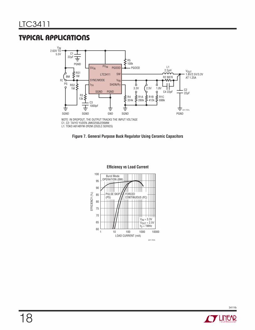
NOTE: IN DROPOUT, THE OUTPUT TRACKS THE INPUT VOLTAGEC1, C2: TAIYO YUDEN JMK325BJ226MML1: TOKO A914BYW-2R2M (D52LC SERIES)
GND
3.3V 2.5V 1.8V
Figure 7. General Purpose Buck Regulator Using Ceramic Capacitors
LOAD CURRENT (mA)
EFF
ICIE
NC
Y (
%)
100
95
90
85
80
75
70
65
601 100 1000 10000
3411 F07b
10
PULSE SKIP(PS)
FORCEDCONTINUOUS (FC)
VIN = 3.3VVOUT = 2.5VfO = 1MHz
Burst ModeOPERATION (BM)
Effi ciency vs Load Current

LTC3411
193411fb
TYPICAL APPLICATIONSSingle Inductor, Positive, Buck-Boost Converter
PVIN
LTC3411
PGND
SWSVIN
SGND
PGOODPGOOD
VFB SYNC/MODE
ITH SHDN/RT
L13.3μH D1
VOUT3.3V/400mA
VIN
VIN2.63VTO 5V
100k
M1
R4324k
R313k
3411 TA02
C31000pFC7
10pF
C1, C2: TAIYO YUDEN JMK325BJ226MMC4: SANYO POSCAP 6TPA47MD1: ON MBRM120L
L1: TOKO A915AY-3R3M (D53LC SERIES)M1: SILICONIX Si2302DS
R1280k
C447μF
+
C122μF
C222μF
2
R2887k
Effi ciency vs Load Current
LOAD CURRENT (mA)
10
EFF
ICIE
NC
Y (
%)
85
80
75
70
65
60
55100 1000
3411 TA03
VIN = 4V
VIN = 3V
VIN = 3.5V
VIN = 2.5V
fO = 1MHz

LTC3411
203411fb
TYPICAL APPLICATIONSAll Ceramic 2-Cell to 3.3V and 1.8V Converters
Effi ciency vs Load Current
LTC3402
VIN
SHDN
MODE/SYNC
PGOOD
RT
SW
VOUT
FB
VC
GND1000pF
10pF
2CELLS
C110μF
47k49.9k
604k
1M
VOUT3.3V120mA/1A
L14.7μH D1
C244mF(2 22mF)
C1: TAIYO YUDEN JMK212BJ106MGC2: TAIYO YUDEN JMK325BJ226MMC5, C6: TAIYO YUDEN JMK325BJ226MM
VIN = 2V TO 3V
0 = FIXED FREQ1 = Burst Mode OPERATION
+
SYNC/MODE
LTC3411
PVIN
SW
SVIN
PGOOD
ITH
SHDN/RT
PGNDSGND
VFB
L22.2μH
VOUT1.8V/1.2A
887k
412k1000pF
3411 TA06
C622μF
13k
C522μF
324k
D1: ON SEMICONDUCTOR MBRM120LT3L1: TOKO A916CY-4R7ML2: TOKO A914BYW-2R2M (D52LC SERIES)
LOAD CURRENT (mA)
10
80
EFF
ICIE
NC
Y (
%)
90
100
100 1000 10000
3211 TA07
70
75
85
95
65
60
3.3V 1.8V
VIN = 2.4VBurst Mode OPERATION

LTC3411
213411fb
TYPICAL APPLICATION2mm Height, 2MHz, Li-Ion to 1.8V Converter
Effi ciency vs Load Current
PVIN
LTC3411
PGOOD PGOOD
SWSVIN
SYNC/MODE
VFBITH
SHDN/RT
L11μH
VOUT1.8VAT 1.25A
VIN2.63V
TO 4.2V
SGND PGND
R5100k
C4 22pF
R4154k
R315k
R1698k
R2887k
3411 TA04
C3470pF
C747pF
C51μF
+
C133μF
+C61μF
C1, C2: AVX TPSB336K006R0600C4, C5: TAIYO YUDEN LMK212BJ105MGL1: COILCRAFT DO1606T-102
C233μF
LOAD CURRENT (mA)
EFF
ICIE
NC
Y (
%)
100
95
90
85
80
75
70
65
60
55
501 100 1000 10000
3411 TA05
10
VOUT = 1.8VfO = 2MHz
2.5V
3.6V
4.2V

LTC3411
223411fb
PACKAGE DESCRIPTIONDD Package
10-Lead Plastic DFN (3mm × 3mm)(Reference LTC DWG # 05-08-1699)
3.00 0.10(4 SIDES)
NOTE:1. DRAWING TO BE MADE A JEDEC PACKAGE OUTLINE M0-229 VARIATION OF (WEED-2). CHECK THE LTC WEBSITE DATA SHEET FOR CURRENT STATUS OF VARIATION ASSIGNMENT2. DRAWING NOT TO SCALE3. ALL DIMENSIONS ARE IN MILLIMETERS4. DIMENSIONS OF EXPOSED PAD ON BOTTOM OF PACKAGE DO NOT INCLUDE MOLD FLASH. MOLD FLASH, IF PRESENT, SHALL NOT EXCEED 0.15mm ON ANY SIDE5. EXPOSED PAD SHALL BE SOLDER PLATED6. SHADED AREA IS ONLY A REFERENCE FOR PIN 1 LOCATION ON THE TOP AND BOTTOM OF PACKAGE
0.38 0.10
BOTTOM VIEW—EXPOSED PAD
1.65 0.10(2 SIDES)
0.75 0.05
R = 0.115TYP
2.38 0.10(2 SIDES)
15
106
PIN 1TOP MARK
(SEE NOTE 6)
0.200 REF
0.00 – 0.05
(DD) DFN 1103
0.25 0.05
2.38 0.05(2 SIDES)
RECOMMENDED SOLDER PAD PITCH AND DIMENSIONS
1.65 0.05(2 SIDES)2.15 0.05
0.50BSC
0.675 0.05
3.50 0.05
PACKAGEOUTLINE
0.25 0.050.50 BSC

LTC3411
233411fb
Information furnished by Linear Technology Corporation is believed to be accurate and reliable. However, no responsibility is assumed for its use. Linear Technology Corporation makes no representa-tion that the interconnection of its circuits as described herein will not infringe on existing patent rights.
PACKAGE DESCRIPTIONMS Package
10-Lead Plastic MSOP(Reference LTC DWG # 05-08-1661)
MSOP (MS) 0307 REV E
0.53 0.152
(.021 .006)
SEATINGPLANE
0.18
(.007)
1.10
(.043)MAX
0.17 – 0.27
(.007 – .011)
TYP
0.86
(.034)REF
0.50
(.0197)BSC
1 2 3 4 5
4.90 0.152
(.193 .006)
0.497 0.076
(.0196 .003)
REF8910 7 6
3.00 0.102
(.118 .004)
(NOTE 3)
3.00 0.102
(.118 .004)
(NOTE 4)
NOTE:1. DIMENSIONS IN MILLIMETER/(INCH)2. DRAWING NOT TO SCALE3. DIMENSION DOES NOT INCLUDE MOLD FLASH, PROTRUSIONS OR GATE BURRS. MOLD FLASH, PROTRUSIONS OR GATE BURRS SHALL NOT EXCEED 0.152mm (.006") PER SIDE4. DIMENSION DOES NOT INCLUDE INTERLEAD FLASH OR PROTRUSIONS. INTERLEAD FLASH OR PROTRUSIONS SHALL NOT EXCEED 0.152mm (.006") PER SIDE5. LEAD COPLANARITY (BOTTOM OF LEADS AFTER FORMING) SHALL BE 0.102mm (.004") MAX
0.254
(.010)0° – 6° TYP
DETAIL “A”
DETAIL “A”
GAUGE PLANE
5.23(.206)MIN
3.20 – 3.45(.126 – .136)
0.889 0.127(.035 .005)
RECOMMENDED SOLDER PAD LAYOUT
0.305 0.038(.0120 .0015)
TYP
0.50(.0197)
BSC
0.1016 0.0508
(.004 .002)

LTC3411
243411fb
Linear Technology Corporation1630 McCarthy Blvd., Milpitas, CA 95035-7417 (408) 432-1900 ● FAX: (408) 434-0507 ● www.linear.com © LINEAR TECHNOLOGY CORPORATION 2002
LT 1108 REV B • PRINTED IN USA
RELATED PARTSPART NUMBER DESCRIPTION COMMENTS
LT1616 500mA (IOUT) 1.4MHz High Effi ciency Step-Down DC/DC Converter 90% Effi ciency, VIN: 3.6V to 25V, VOUT(MIN): 1.25V, IQ: 1.9mA, ISD: <1μA, ThinSOT
LT1776 500mA (IOUT) 200kHz High Effi ciency Step-Down DC/DC Converter 90% Effi ciency, VIN: 7.4V to 40V, VOUT(MIN): 1.24V, IQ: 3.2mA, ISD: 30μA, N8, S8
LTC1879 1.2A (IOUT) 550kHz Synchronous Step-Down DC/DC Converter 95% Effi ciency, VIN: 2.7V to 10V, VOUT(MIN): 0.8V, IQ: 15μA, ISD: <1μA, TSSOP16
LTC3405/LTC3405A 300mA (IOUT) 1.5MHz Synchronous Step-Down DC/DC Converters 95% Effi ciency, VIN: 2.7V to 6V, VOUT(MIN): 0.8V, IQ: 20μA, ISD: <1μA, ThinSOT
LTC3406/LTC3406B 600mA (IOUT) 1.5MHz Synchronous Step-Down DC/DC Converters 95% Effi ciency, VIN: 2.5V to 5.5V, VOUT(MIN): 0.6V, IQ: 20μA, ISD: <1μA, ThinSOT
LTC3412 2.5A (IOUT) 4MHz Synchronous Step-Down DC/DC Converter 95% Effi ciency, VIN: 2.5V to 5.5V, VOUT(MIN): 0.8V, IQ: 60μA, ISD: <1μA, TSSOP16E
LTC3413 3A (IOUT Sink/Source) 2MHz Monolithic Synchronous Regulator for DDR/QDR Memory Termination
90% Effi ciency, VIN: 2.25V to 5.5V, VOUT(MIN): VREF/2,IQ: 280μA, ISD: <1μA, TSSOP16E
LTC3430 60V, 2.75A (IOUT) 200kHz High Effi ciency Step-Down DC/DC Converter 90% Effi ciency, VIN: 5.5V to 60V, VOUT(MIN): 1.20V, IQ: 2.5mA, ISD: 25μA, TSSOP16E
LTC3440 600mA (IOUT) 2MHz Synchronous Buck-Boost DC/DC Converter 95% Effi ciency, VIN: 2.5V to 5.5V, VOUT(MIN): 2.5V, IQ: 25μA, ISD: <1μA, 10-Lead MS
ThinSOT is a trademark of Linear Technology Corporation.