User Guide | EVAL-SSM6515 - Analog Devices
23
User Guide | EVAL-SSM6515 UG-2030 Evaluating the SSM6515 Ultra Low Power, Class-D Audio Amplifier PLEASE SEE THE LAST PAGE FOR AN IMPORTANT WARNING AND LEGAL TERMS AND CONDITIONS. Rev. 0 | 1 of 23 EVALUATION KIT CONTENTS ► EVAL-SSM6515Z evaluation board ► EVAL-ADUSB2EBZ (USBi) communications adapter ► USB cable with mini USB plug DOCUMENTS NEEDED ► SSM6515 data sheet GENERAL DESCRIPTION This user guide explains the design and setup of the EVAL- SSM6515Z evaluation board. The EVAL-SSM6515Z provides access to all analog and digital inputs/outputs on the SSM6515. The SSM6515 amplifier is controlled by Analog Devices, Inc., SigmaStudio ® software, which interfaces to the EVAL-SSM6515Z via a USB connection. The EVAL-SSM6515Z can be powered by the USB bus or by a single 3.8 V to 5 V supply. These supplies are regulated to the voltages required on the EVAL-SSM6515Z. The printed circuit board (PCB) is a 4-layer design, with a ground plane and a power plane on the inner layers. The EVAL-SSM6515Z con- tains 0.1 in. pitch male headers for connecting to external speakers. The minimum speaker load must be 8 Ω. The EVAL-SSM6515Z consists of two SSM6515s for evaluating the stereo headphone output. For full details on the SSM6515, see the SSM6515 data sheet, which must be consulted in conjunction with this user guide when using the EVAL-SSM6515Z. EVALUATION BOARD PHOTOGRAPH Figure 1. Analog Devices is in the process of updating documentation to provide terminology and language that is culturally appropriate. This is a process with a wide scope and will be phased in as quickly as possible. Thank you for your patience.
-
Upload
khangminh22 -
Category
Documents
-
view
0 -
download
0
Transcript of User Guide | EVAL-SSM6515 - Analog Devices

User Guide | EVAL-SSM6515UG-2030
Evaluating the SSM6515 Ultra Low Power, Class-D Audio Amplifier
PLEASE SEE THE LAST PAGE FOR AN IMPORTANTWARNING AND LEGAL TERMS AND CONDITIONS.
Rev. 0 | 1 of 23
EVALUATION KIT CONTENTS
EVAL-SSM6515Z evaluation board EVAL-ADUSB2EBZ (USBi) communications adapter USB cable with mini USB plug
DOCUMENTS NEEDED
SSM6515 data sheet
GENERAL DESCRIPTION
This user guide explains the design and setup of the EVAL-SSM6515Z evaluation board.The EVAL-SSM6515Z provides access to all analog and digitalinputs/outputs on the SSM6515.
The SSM6515 amplifier is controlled by Analog Devices, Inc.,SigmaStudio® software, which interfaces to the EVAL-SSM6515Zvia a USB connection. The EVAL-SSM6515Z can be powered bythe USB bus or by a single 3.8 V to 5 V supply. These supplies areregulated to the voltages required on the EVAL-SSM6515Z. Theprinted circuit board (PCB) is a 4-layer design, with a ground planeand a power plane on the inner layers. The EVAL-SSM6515Z con-tains 0.1 in. pitch male headers for connecting to external speakers.The minimum speaker load must be 8 Ω. The EVAL-SSM6515Zconsists of two SSM6515s for evaluating the stereo headphoneoutput.For full details on the SSM6515, see the SSM6515 data sheet,which must be consulted in conjunction with this user guide whenusing the EVAL-SSM6515Z.
EVALUATION BOARD PHOTOGRAPH
Figure 1.
Analog Devices is in the process of updating documentation to provide terminology and language that is culturally appropriate. This is a processwith a wide scope and will be phased in as quickly as possible. Thank you for your patience.

User Guide EVAL-SSM6515TABLE OF CONTENTS
analog.com Rev. 0 | 2 of 23
Evaluation Kit Contents......................................... 1Documents Needed...............................................1General Description...............................................1Evaluation Board Photograph................................1Evaluation Board Block Diagram...........................3Hardware Description............................................ 4
Jumpers and Connectors................................... 4Installing the SigmaStudio Software......................6
Installing the USBi (EVAL-ADUSB2EBZ)Drivers..............................................................6
Adding the DLL File............................................7Setting Up SigmaStudio..................................... 8
Setting Up the Evaluation Board......................... 10Default Switch and Jumper Settings (S/PDIF Input, I2C Mode)....................................10
Powering Up the EVAL-SSM6515Z..................11Power............................................................... 11Using I2C Control Mode....................................11Using SigmaStudio with USBi for I2C Control.. 11External I2S Input, I2C Mode............................ 13Default Switch and Jumper Settings (PDMInput, I2C Mode)............................................. 13
Default Switch and Jumper Settings (S/PDIF Input, Standalone Mode).......................14
Evaluation Board Schematics and Artwork......... 15Ordering Information............................................22
Bill of Materials.................................................22
REVISION HISTORY
4/2022—Revision 0: Initial Version
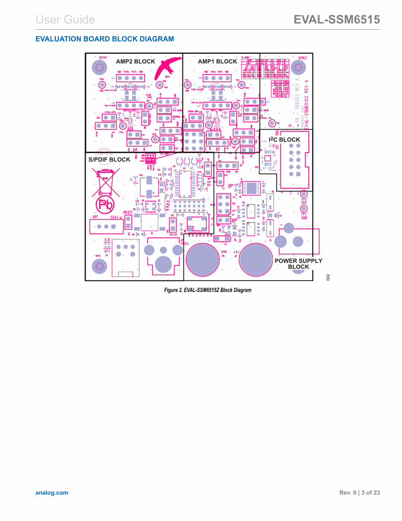
User Guide EVAL-SSM6515EVALUATION BOARD BLOCK DIAGRAM
analog.com Rev. 0 | 3 of 23
Figure 2. EVAL-SSM6515Z Block Diagram

User Guide EVAL-SSM6515HARDWARE DESCRIPTION
analog.com Rev. 0 | 4 of 23
JUMPERS AND CONNECTORSTable 1. Connector and Jack DescriptionsReferenceDesignator Type Functional Name DescriptionJ1 DC jack 5 V dc input Barrel jack that provides external power to the EVAL-SSM6515. J1 accepts a 3.8 V dc to 5 V
dc input.J2 Binding post 5 V Binding post used to connect the external 5 V supply to the EVAL-SSM6515.J5 2-pin header, 0.1 in. pitch PVDD (AMP1) Jumper connects PVDD to the SSM6515 (AMP1).J6 6-pin header, 0.1 in. pitch IOVDD select Used to select the IOVDD source: 1.2 V regulator, 1.8 V regulator, or external 1.8 V IOVDD
source.J7 2-pin header, 0.1 in. pitch External PVDD Used to connect the external 1.8 V PVDD supply.J8 3-pin header, 0.1 in pitch Pulse density modulation
(PDM) LR_SEL (AMP1)Used to select the PDM left and right channels for AMP1 in standalone mode.
J9 3-pin header, 0.1 in. pitch Mode select (AMP1) Used to select the I2S or PDM mode for AMP1 in standalone mode.J10 Binding post GND Connect to GND or 0 V of the power supply.J11 10-pin header, 0.1 in. pitch USB interface (USBi) header 10-pin header used to connect the USBi.J12 RCA cinch jack Coaxial S/PDIF input Used to connect the coaxial S/PDIF input.J13 9-pin header, 0.1 in. pitch S/PDIF, external I2S, PDM
Input9-pin header for selecting the internal input source (S/PDIF) or connecting the externalI2S/PDM input source for the amplifiers.
J14 2-pin header, 0.1 in. pitch S/PDIF master clock (MCLK)out
Used to access the recovered master clock from the S/PDIF receiver.
J15 3-pin header, 0.1 in. pitch I2S/PDM select (AMP1) Used to select the left and right channel in I2S standalone mode or the PDM_FS of 3 MHz or 6MHz for AMP1 in PDM standalone mode.
J18 2-pin header, 0.1 in. pitch PVDD (AMP2) Jumper connects PVDD to the SSM6515 (AMP2).J19 3-pin header, 0.1 in. pitch PDM LR_SEL (AMP2) Used to select the PDM left and right channels for AMP2 in standalone mode.J20 3-pin header, 0.1 in. pitch I2S/PDM select (AMP2) Used to select the I2S or PDM input for AMP2 in standalone mode.J21 3-pin header, 0.1 in. pitch I2S/PDM select (AMP2) Used to select the left and right channels in I2S standalone mode or the PDM_FS of 3 MHz or
6 MHz for AMP2 in PDM standalone mode.J22 2-pin header, 0.1 in. pitch I2C SCL (AMP2) Jumper connects the USBi SCL to AMP2. Leave open in standalone mode.J23 2-pin header, 0.1 in. pitch I2C SDA (AMP2) Jumper connects the USBi SDA to AMP2. Leave open in standalone mode.J24 2-pin header, 0.1 in. pitch I2C SCL (AMP1) Jumper connects the USBi SCL to AMP1. Leave open in standalone mode.J25 2-pin header, 0.1 in. pitch I2C SDA (AMP1) Jumper connects the USBi SDA to AMP1. Leave open in standalone mode.J26 2-pin header, 0.1 in. pitch FSYNC Jumper connects FSYNC to AMP2. Leave open for PDM in standalone mode.J27 2-pin header, 0.1 in. pitch FSYNC Jumper connects FSYNC to AMP1. Leave open for PDM in standalone mode.J28 2-pin header, 0.1 in. pitch IOVDD (AMP1) Jumper connects IOVDD to the SSM6515 (AMP1).J29 2-pin header, 0.1 in. pitch IOVDD (AMP2) Jumper connects IOVDD to the SSM6515 (AMP2).J30 2-pin header, 0.1 in. pitch Do not use Leave this jumper open (Reserved for internal use).J31 2-pin header, 0.1 in. pitch Do not use Leave this jumper open (Reserved for internal use).J32 2-pin header, 0.1 in. pitch External IOVDD Used to connect the external 1.2 V to 1.8 V IOVDD supply.J33 3-pin header, 0.1 in. pitch I2C address select (AMP2) J33 and J34 are used to select the I2C address for AMP2. Connect J33 to PVDD in standalone
mode.J34 2-pin header, 0.1 in. pitch I2C address select (AMP2) J33 and J34 are used to select the I2C address for AMP2. Shunt J34 in standalone mode.J35 3-pin header, 0.1 in. pitch I2C address select (AMP1) J35 and J36 are used to select the I2C address for AMP1. Connect J35 to PVDD in standalone
mode.J36 2-pin header, 0.1 in. pitch I2C address select (AMP1) J35 and J36 are used to select the I2C address for AMP1. Shunt J36 in standalone mode.J37 4-pin header, 0.1 in. pitch AMP1 output AMP1 pre-filter output.J38 4-pin header, 0.1 in. pitch AMP1 output AMP1 pre-filter output.J39 4-pin header, 0.1 in. pitch AMP2 output AMP2 post-filter output.J40 4-pin header, 0.1 in. pitch AMP2 output AMP2 post-filter output.JP1 3-pin header, 0.1 in. pitch PVDD select Used to select the 1.8 V regulator or external 1.8 V PVDD source.JP2 2-pin header, 0.1 in. pitch S/PDIF reset jumper Shunt JP2 to keep the S/PDIF receiver in reset.JP3 2-pin header, 0.1 in. pitch SD_OSC (active low) Shunt JP3 to disable the 12.288 MHz oscillator input to the S/PDIF receiver.

User Guide EVAL-SSM6515HARDWARE DESCRIPTION
analog.com Rev. 0 | 5 of 23
Table 1. Connector and Jack DescriptionsReferenceDesignator Type Functional Name DescriptionS3 Single pole double throw
(SPDT) slide switchS/PDIF source select Select the optical S/PDIF input or coaxial S/PDIF input.
S4 Momentary switch S/PDIF reset button Push S4 to reset the S/PDIF receiver.U4 Optical fiber connector S/PDIF optical input S/PDIF optical input.
J13 (I2S Input Selection Header)The J13 is a 9-pin header. Pin 1, Pin 4, and Pin 7 of J13 areGND, whereas Pin 2, Pin 5, and Pin 8 are used as signal inputs.The outermost pins, Pin 3, Pin 6, and Pin 9, are connected to theS/PDIF receiver I2S outputs. See Table 2 for the pin connections.The I2S signals must be 1.8 V p-p.
Table 2. J13 9-Pin (3×3) Header ConnectionsPin Signal Test Conditions/Comments1, 4, 7 GND GND2 SDATA SSM6515 serial data input5 FSYNC SSM6515 frame sync input8 BCLK SSM6515 bit clock input3 SDATA S/PDIF S/PDIF serial data output6 FSYNC S/PDIF S/PDIF frame sync output9 BCLK S/PDIF S/PDIF bit clock output

User Guide EVAL-SSM6515INSTALLING THE SIGMASTUDIO SOFTWARE
analog.com Rev. 0 | 6 of 23
Download and install the latest version of SigmaStudio by complet-ing the following steps:1. Install the latest version of the Microsoft® .NET framework if it is
not already installed on the PC. The latest version of the .NETframework can be downloaded from the Microsoft website.
2. Go to www.analog.com/SigmaStudio and download the latestversion of SigmaStudio from the Downloads And RelatedSoftware section.
3. Download the installer and run the executable file. Follow theprompts, including accepting the license agreement, to installthe software.
INSTALLING THE USBI (EVAL-ADUSB2EBZ)DRIVERSSigmaStudio must be installed to use the USBi. When the SigmaS-tudio installation completes, perform the following steps:1. Connect the USBi to an available USB 2.0 port using the USB
cable included in the evaluation board kit (the USBi does notfunction properly with a USB 3.0 port).
2. Install the driver software (see the Using Windows XP sectionor the Using Windows 7 or Windows Vista section for moreinformation).
Using Windows XPAfter connecting the USBi to the USB 2.0 port, Windows® XPrecognizes the device (see Figure 3) and prompts the user to installthe drivers.
Figure 3. Found New Hardware Notification
Use the Found New Hardware Wizard to complete the installationof the drivers. The installation of the drivers is shown in the follow-ing steps:1. From the Found New Hardware Wizard window, select the
Install from a list or specific location (Advanced) option andclick Next > (see Figure 4).
Figure 4. Found New Hardware Wizard: Installation2. Select Search for the best driver in these locations, select
Include this location in the search:, and click Browse to findthe USB drivers subdirectory within the SigmaStudio directory(see Figure 5). Then, click Next >.
Figure 5. Found New Hardware Wizard: Search and Installation Options3. When the Hardware Installation warning appears, click Con-
tinue Anyway (see Figure 6).
Figure 6. Hardware Installation Warning

User Guide EVAL-SSM6515INSTALLING THE SIGMASTUDIO SOFTWARE
analog.com Rev. 0 | 7 of 23
The USBi drivers are now installed. Leave the USBi connected tothe PC.
Using Windows 7 or Windows VistaAfter connecting the USBi to the USB 2.0 port, Windows 7 orWindows Vista recognizes the device and installs the drivers auto-matically (see Figure 7). When the installation completes, leave theUSBi connected to the PC.
Figure 7. USBi Drivers Installed Properly
Confirming Proper Installation of the USBiDriversTo confirm that the USBi drivers are installed properly, complete thefollowing steps:1. With the USBi still connected to the USB 2.0 port of the PC,
check that both the yellow I2C LED and the red power indicatorLED are illuminated (see Figure 8).
Figure 8. State of USBi Status LEDs After Driver Installation
2. In the Windows Device Manager, under the Universal SerialBus controllers section, check that Analog Devices USBi(programmed) appears as shown in Figure 9.
Figure 9. Confirming Driver Installation Using the Device Manager
ADDING THE DLL FILEAdd the provided SSM6515.dll file manually by copying theSSM6515.dll file to the C:\ProgramFiles\AnalogDevices\SigmaS-tudio folder in the PC. To add the SSM6515 to the Tree ToolBox,click Tools and then click Add-Ins Browser... (as shown in Figure10). The AddIns popup window opens (see Figure 11).In the list of devices displayed in the AddIns popup window, ensurethe SSM6515 checkbox is selected, as shown in Figure 11. ClickFile and then click Save before exiting the window.
Figure 10. Adding an SSM6515
Figure 11. Saving the SSM6515.dll File in the AddIns Popup Window

User Guide EVAL-SSM6515INSTALLING THE SIGMASTUDIO SOFTWARE
analog.com Rev. 0 | 8 of 23
SETTING UP SIGMASTUDIOStart SigmaStudio by double clicking the shortcut on the desktop.Click File and then click New Project, or press Ctrl + N to createa new project, as shown in Figure 12. The default view of the newproject is the Hardware Configuration tab. Figure 13 shows a newSigmaStudio project. Figure 12. New Project
Figure 13. New SigmaStudio Project

User Guide EVAL-SSM6515INSTALLING THE SIGMASTUDIO SOFTWARE
analog.com Rev. 0 | 9 of 23
To use the USBi with SigmaStudio, select USBi from the Commu-nication Channels list of the Tree Toolbox (see Figure 14), anddrag it to the right to add it to the project space.
Figure 14. Adding the USBi Communication Channel
If SigmaStudio cannot detect the USBi board on the USB port of thePC, the background of the USB label is red (see Figure 15). Thelabel turns red when the USBi is not connected or when the driversare installed incorrectly.
Figure 15. USBi Not Detected by SigmaStudio
If SigmaStudio detects the USBi board on the USB port of the PC,the background of the USB label is green (see Figure 16).
Figure 16. USBi Detected by SigmaStudio
Add two SSM6515s from the Tree ToolBox to the HardwareConfiguration tab by selecting SSM6515 from the Processors(ICs / DSPs) list and dragging it to the project space (see Figure10).To use the USBi board to communicate with the target IC, connectthe IC by clicking and dragging a wire between the blue pin of theUSBi and the green pin of the IC (see Figure 17). The correspond-ing dropdown box of the USBi automatically fills with the defaultmode and channel for that IC.
Figure 17. Connecting the USBi to an SSM6515 IC

User Guide EVAL-SSM6515SETTING UP THE EVALUATION BOARD
analog.com Rev. 0 | 10 of 23
DEFAULT SWITCH AND JUMPER SETTINGS (S/PDIF INPUT, I2C MODE)The EVAL-SSM6515Z consists of two SSM6515s for stereo head-phone output. Refer to Figure 19 for the switch and jumper settings.These settings set the EVAL-SSM6515Z for external I2S input withI2C control using the USBi.The EVAL-SSM6515Z provides multiple options for configuring theSSM6515. See Table 3 for the I2C mode and device addresssettings. By default, the EVAL-SSM6515Z is configured for Address0x34 (AMP1) and Address 0x35 (AMP2). If other addresses arerequired, refer to Table 3.
To use the on-board S/PDIF receiver I2S input, insert jumpers forJ13 as shown in Figure 18.
Figure 18. S/PDIF as I2S Source
Figure 19. S/PDIF Input, I2C Mode

User Guide EVAL-SSM6515SETTING UP THE EVALUATION BOARD
analog.com Rev. 0 | 11 of 23
Table 3. I2C or Standalone Mode Selection, AMP11
Parameter I2C Device Address J24, J25 J35 J36I2C Mode 0x34 Installed GND InstalledI2C Mode 0x35 Installed GND OpenI2C Mode 0x36 Installed Open OpenI2C Mode 0x37 Installed PVDD OpenStandalone Mode N/A Open PVDD Installed1 N/A means not applicable.
Table 4. I2C or Standalone Mode Selection, AMP21
Parameter I2C Device Address J22, J23 J33 J34I2C Mode 0x34 Installed GND InstalledI2C Mode 0x35 Installed GND OpenI2C Mode 0x36 Installed Open OpenI2C Mode 0x37 Installed PVDD OpenStandalone Mode N/A Open PVDD Installed1 N/A means not applicable.
Table 5. I2S or PDM Input Selection in Standalone Mode
ModeAMP2 J22, J23 J20 J21 J26 J19AMP1 J24, J25 J9 J15 J27 J8
I2S Left channel Open GND GND Installed OpenRight channel Open GND IOVDD Installed Open
PDM Left channel, 3 MHz Open IOVDD GND Open GNDRight channel, 3 MHz Open IOVDD GND Open IOVDDLeft channel, 6 MHz Open IOVDD IOVDD Open GNDRight channel, 6 MHz Open IOVDD IOVDD Open IOVDD
POWERING UP THE EVAL-SSM6515ZTo power up the EVAL-SSM6515Z, connect the ribbon cable of theUSBi board to J1 (control port) of the EVAL-SSM6515Z.
POWERPower can be supplied to the EVAL-SSM6515Z in one of threeways: connecting the EVAL-ADUSB2EBZ (USBi) board to J11 (seeFigure 20), connecting a 3.8 V dc to 5 V dc power supply to J1(tip positive), or using the binding posts, J2 (5 V) and J10 (GND). Ifno external supply is used, the EVAL-SSM6515Z draws power fromthe USBi board.
Figure 20. Header J11, Control Port
The on-board regulators generate the 1.8 V, 1.2 V, and 3.3 V dcsupplies. The JP1 and J6 jumpers are used to set the PVDD andIOVDD supplies to the SSM6515. By default, the 1.8 V supply isused for PVDD and IOVDD. The J5 and J18 jumpers provide thePVDD supply to individual SSM6515 amplifiers, and the J28 andJ29 jumpers provide the IOVDD supply. By removing these jump-ers, the currents to the individual SSM6515s can be measured.
USING I2C CONTROL MODEConnecting the USBi to J11 provides I2C control for the SSM6515.See Figure 20.
USING SIGMASTUDIO WITH USBI FOR I2CCONTROLTake the following steps to use SigmaStudio with the USBi for I2Ccontrol and to configure the registers for I2S operation:1. In the Hardware Configuration tab, click the IC 1 - SSM6515
v1.0.0.1 tab, then click the ChipID tab (see Figure 21). ClickGet ID to read the device ID and revision.
2. Click the Datapath tab. Click Mute Control to select DACUnmuted to unmute the DAC, as shown in Figure 22.

User Guide EVAL-SSM6515SETTING UP THE EVALUATION BOARD
analog.com Rev. 0 | 12 of 23
3. Click the Control/Status tab. Click Software Master Power-down to select Normal to turn on the amplifier if the I2S clocks
are provided. The amplifier outputs the audio at J38 (AMP1)and J40 (AMP2).
Figure 21. ChipID Tab
Figure 22. Datapath Tab

User Guide EVAL-SSM6515SETTING UP THE EVALUATION BOARD
analog.com Rev. 0 | 13 of 23
Figure 23. Control/Status Tab
EXTERNAL I2S INPUT, I2C MODEIf using the external I2S input, the only change needed is for J13.Connect a digital I2S audio source to J13. The external I2S signalsmust be 1.8 V p-p. Refer to Table 2 for the J13 header connections.
Figure 24. External I2S Selection
DEFAULT SWITCH AND JUMPER SETTINGS(PDM INPUT, I2C MODE)If using the PDM source as an input, use the same settings asshown in Figure 19, but connect only the PDM data and clock at Pin2 and Pin 8 of J13. Leave Pin 5 (center) unconnected. Follow Table5 for the desired PDM mode. Then, use SigmaStudio to configurethe PDM mode for the SSM6515, as shown in Figure 22.Turn on the PDM signals to the EVAL-SSM6515Z. The audio outputis available at J38 (AMP1) and J40 (AMP2).

User Guide EVAL-SSM6515SETTING UP THE EVALUATION BOARD
analog.com Rev. 0 | 14 of 23
Figure 25. PDM Configuration
DEFAULT SWITCH AND JUMPER SETTINGS (S/PDIF INPUT, STANDALONE MODE)To configure the EVAL-SSM6515Z for standalone mode, refer toTable 3 and set the desired input I2S or PDM mode using Table 5.
Configure J13 accordingly. If using the on board S/PDIF receiverI2S input, insert the jumpers as shown in Figure 18. If using theexternal I2S input, refer to Figure 24 for J13. If using the PDMsource, connect only the PDM data and PDM clock at Pin 2 and Pin8 of J13, respectively. Leave Pin 5 (center) unconnected.

User Guide EVAL-SSM6515EVALUATION BOARD SCHEMATICS AND ARTWORK
analog.com Rev. 0 | 15 of 23
Figure 26. EVAL-SSM6515Z Schematic: Block Diagram (HP Is Headphone)

User Guide EVAL-SSM6515EVALUATION BOARD SCHEMATICS AND ARTWORK
analog.com Rev. 0 | 16 of 23Figure 27. EVAL-SSM6515Z Schematic Page 1

User Guide EVAL-SSM6515EVALUATION BOARD SCHEMATICS AND ARTWORK
analog.com Rev. 0 | 17 of 23
Figure 28. EVAL-SSM6515Z Schematic Page 2

User Guide EVAL-SSM6515EVALUATION BOARD SCHEMATICS AND ARTWORK
analog.com Rev. 0 | 18 of 23
Figure 29. EVAL-SSM6515Z Layout: Top Assembly
Figure 30. EVAL-SSM6515Z Layout: Top Copper
User Guide EVAL-SSM6515EVALUATION BOARD SCHEMATICS AND ARTWORK
analog.com Rev. 0 | 19 of 23
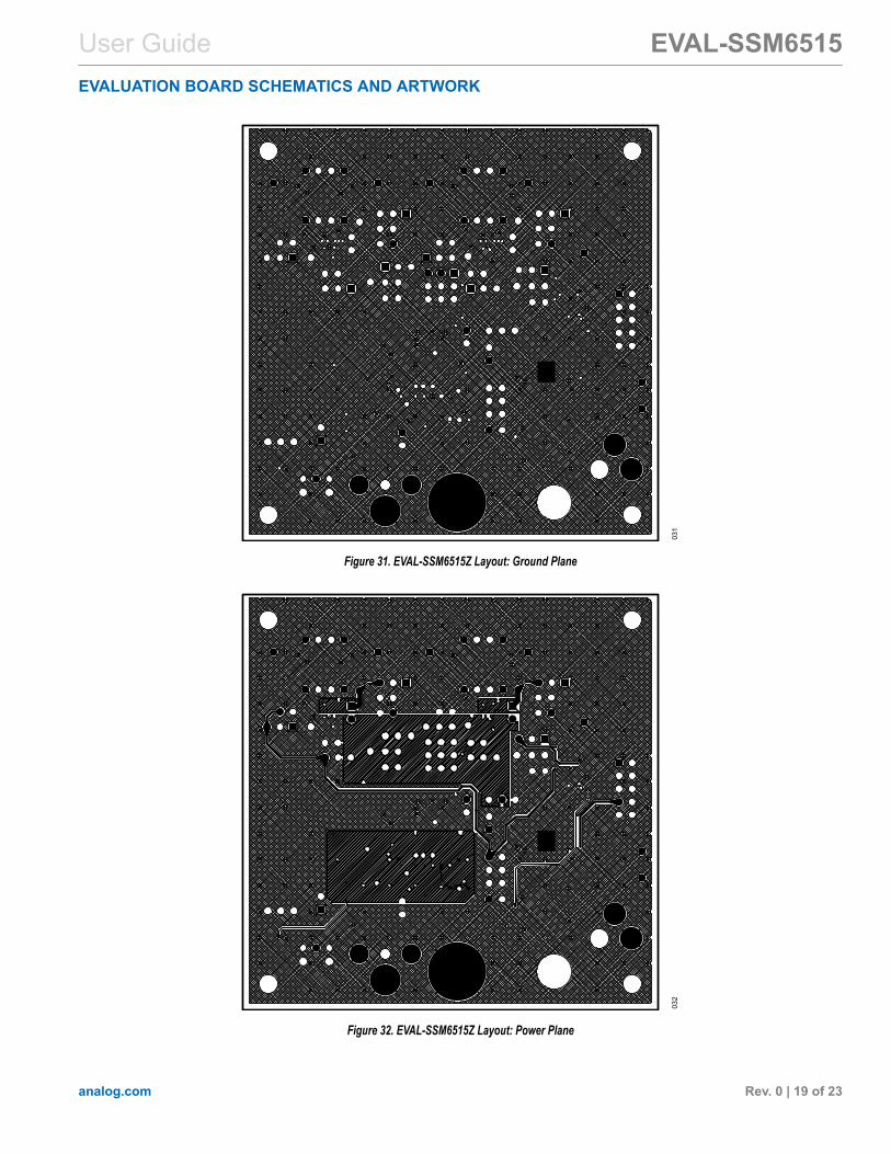
Figure 31. EVAL-SSM6515Z Layout: Ground Plane
Figure 32. EVAL-SSM6515Z Layout: Power Plane

User Guide EVAL-SSM6515EVALUATION BOARD SCHEMATICS AND ARTWORK
analog.com Rev. 0 | 20 of 23
Figure 33. EVAL-SSM6515Z Layout: Bottom Copper

User Guide EVAL-SSM6515EVALUATION BOARD SCHEMATICS AND ARTWORK
analog.com Rev. 0 | 21 of 23
Figure 34. EVAL-SSM6515Z Layout: Fab Drawing

User Guide EVAL-SSM6515ORDERING INFORMATION
analog.com Rev. 0 | 22 of 23
BILL OF MATERIALSTable 6.Qty Reference Description Vendor Vendor Order Number3 C1, C10, C32 Multilayer ceramic capacitors, 1 μF, 16 V, X7R, 0603 Digi-Key 490-3900-1-ND/445-1604-2-ND2 C2, C19 Multilayer ceramic capacitors, 1 nF, 50 V, NP0, 0402 Digi-Key 490-3244-1-ND6 C3, C4, C28, C29,
C37, C38Multilayer ceramic capacitors, 25 V, NP0, 0201, do not install (DNI) Digi-Key 311-1611-1-ND
4 C5, C26, C35, C36 Multilayer ceramic capacitors, 10 μF, 6.3 V, X5R, 0402 Digi-Key 490-13211-1-ND6 C6, C9, C13, C27,
C30, C34Multilayer ceramic capacitors, 100 nF, 6.3 V, X5R, 0201 Digi-Key 490-3167-1-ND
1 C7 Multilayer ceramic capacitors, 10 μF, 10 V, X7R, 0805 Digi-Key 490-3905-1-ND/445-6857-2-ND3 C8, C11, C33 Ceramic capacitors, 4.7 μF, 6.3 V, 10% X5R, 0603 Digi-Key 490-3297-1-ND/490-7205-2-ND9 C12, C14, C17, C21 to
C25, C31Multilayer ceramic capacitors, 0.10 μF, 16 V, X7R, 0402 Digi-Key 490-3261-1-ND/445-4952-1-ND
2 C15, C16 Multilayer ceramic capacitors, 10 nF, 25 V, NP0, 0603 Digi-Key 445-2664-1-ND/399-5779-1-ND1 C18 Multilayer ceramic capacitors, 22 nF, 25 V, NP0, 0805 Digi-Key 490-1644-1-ND1 C20 Aluminum electrolytic capacitor, 47 μF, 105°, surface-mount device (SMD) Digi-Key PCE4000CT-ND2 D1, D2 Schottky, 30 V, 0.5 A, SOD123 diodes Digi-Key MBR0530T1GOSCT-ND1 D3 Red diffused, 6.0 millicandela, 635 nm, 1206 Digi-Key 67-1003-1-ND1 J1 Mini power jack, 0.08 in., through hole, right angle Digi-Key SC1313-ND2 J2, J10 Nickel binding post mini uninsulated base through hole Digi-Key J587-ND19 J5, J7, J14, J18, J22 to
J32, J34, J36, JP2,JP3
2-pin (1×2) unshrounded headers, 0.10 in., use Shunt Tyco 881545-2 Digi-Key S1011E-02-ND
1 J6 6-pin (2×3) unshrouded header Digi-Key S2011E-03-ND9 J8, J9, J15, J19 to J21,
J33, J35, JP13-pin (1×3) single inline position (SIP) headers Digi-Key S1011E-03-ND
1 J11 10-pin (2×5) shroud polarized header Digi-Key MHC10K-ND1 J12 RCA jack, printed circuit board (PCB), through hole, right angle, yellow Connect Tech
ProductsCTP-021A-S-YEL/CP-1403-ND
1 J13 9-pin (3×3) unshrouded header Digi-Key A108960-ND4 J37 to J40 4-pin (1×4) unshrouded headers, single row Digi-Key S1011E-04-ND/S1011E-36-ND4 L1, L2, L6, L7 Chip ferrite beads, low total harmonic distortion (THD),
MAF1005GAD352AT000, 270 mA, 0402, 500 Ω at 100 MHzDigi-Key 445-174614-1-ND
3 L5, L3, L4 Chip ferrite beads, 600 Ω at 100 MHz Digi-Key 445-2162-1-ND/490-7806-2-ND4 MTH1 to MTH4 Nylon screw pans Phillips 4-40 Digi-Key H542-ND4 MTH1 to MTH4 Nylon hexagonal standoff 4-40, ½ in. Digi-Key 1902CK-ND2 R1, R5 Chip resistors, 2.67 kΩ, 1%, 1/20 W, thick film, 0201 Digi-Key 541-CRCW02012K67FNEDCT-ND1 R1A Chip resistor, 3.01 kΩ, 1% ,100 mW thick film, 0603 Digi-Key RHM3.01KHCT-ND/311-3.01KHRCT-ND6 R2 to R4, R23 to R25 Resistors, 33 Ω, 1/20 W, 5%, 0201, SMD Digi-Key 311-33NCT-ND2 R6, R21 Chip resistors, 47 kΩ, 1%, 50 mW thick film, 0201 Digi-Key 311-47KMCT-ND2 R7, R22 Chip resistors, 10 kΩ, 1%, 50 mW, thick film, 0201 Digi-Key 311-10KNCT-ND1 R8 Chip resistors, 75 Ω, 1%, 100 mW, thick film, 0603 Digi-Key P75.0HCT-ND1 R9 Chip resistors, 10 kΩ, 1%, 63 mW, thick film, 0402 Digi-Key RHM10.0KLCT-ND/541-10.0KLTR-ND1 R10 Chip resistors, 100 kΩ, 1%, 100 mW, thick film, 0402 Digi-Key P100KLCT-ND7 R11, R12, R15 to R19 Chip resistors, 47.5 kΩ, 1%, 100 mW, thick film, 0603 Digi-Key P47.5KHCT-ND2 R13, R20 Chip resistors, 47 kΩ, 1%, 63 mW, thick film, 0402 Digi-Key 311-47.0KLRCT-ND1 R14 Chip resistors, 49.9 Ω, 1%, 63 mW, thick film, 0402 Digi-Key 311-49.9LRCT-ND1 R26 Chip resistors, 475 Ω, 1%, 63 mW, thick film, 0402 Digi-Key 541-475LCT-ND1 R27 Chip resistors, 305 kΩ, 1%, 125 mW, thick film, 0805 Digi-Key 541-1892-1-ND1 R28 Chip resistors, 19.6 kΩ, 1%, 63 mW, thick film, 0402 Digi-Key P19.6KLCT-ND

User Guide EVAL-SSM6515ORDERING INFORMATION
ESD CautionESD (electrostatic discharge) sensitive device. Charged devices and circuit boards can discharge without detection. Although this product features patented or proprietaryprotection circuitry, damage may occur on devices subjected to high energy ESD. Therefore, proper ESD precautions should be taken to avoid performance degradation or loss offunctionality.
Legal Terms and ConditionsBy using the evaluation board discussed herein (together with any tools, components documentation or support materials, the “Evaluation Board”), you are agreeing to be bound by the terms andconditions set forth below (“Agreement”) unless you have purchased the Evaluation Board, in which case the Analog Devices Standard Terms and Conditions of Sale shall govern. Do not use theEvaluation Board until you have read and agreed to the Agreement. Your use of the Evaluation Board shall signify your acceptance of the Agreement. This Agreement is made by and between you(“Customer”) and Analog Devices, Inc. (“ADI”), with its principal place of business at Subject to the terms and conditions of the Agreement, ADI hereby grants to Customer a free, limited, personal,temporary, non-exclusive, non-sublicensable, non-transferable license to use the Evaluation Board FOR EVALUATION PURPOSES ONLY. Customer understands and agrees that the EvaluationBoard is provided for the sole and exclusive purpose referenced above, and agrees not to use the Evaluation Board for any other purpose. Furthermore, the license granted is expressly madesubject to the following additional limitations: Customer shall not (i) rent, lease, display, sell, transfer, assign, sublicense, or distribute the Evaluation Board; and (ii) permit any Third Party to accessthe Evaluation Board. As used herein, the term “Third Party” includes any entity other than ADI, Customer, their employees, affiliates and in-house consultants. The Evaluation Board is NOT soldto Customer; all rights not expressly granted herein, including ownership of the Evaluation Board, are reserved by ADI. CONFIDENTIALITY. This Agreement and the Evaluation Board shall all beconsidered the confidential and proprietary information of ADI. Customer may not disclose or transfer any portion of the Evaluation Board to any other party for any reason. Upon discontinuationof use of the Evaluation Board or termination of this Agreement, Customer agrees to promptly return the Evaluation Board to ADI. ADDITIONAL RESTRICTIONS. Customer may not disassemble,decompile or reverse engineer chips on the Evaluation Board. Customer shall inform ADI of any occurred damages or any modifications or alterations it makes to the Evaluation Board, includingbut not limited to soldering or any other activity that affects the material content of the Evaluation Board. Modifications to the Evaluation Board must comply with applicable law, including butnot limited to the RoHS Directive. TERMINATION. ADI may terminate this Agreement at any time upon giving written notice to Customer. Customer agrees to return to ADI the Evaluation Boardat that time. LIMITATION OF LIABILITY. THE EVALUATION BOARD PROVIDED HEREUNDER IS PROVIDED “AS IS” AND ADI MAKES NO WARRANTIES OR REPRESENTATIONS OF ANYKIND WITH RESPECT TO IT. ADI SPECIFICALLY DISCLAIMS ANY REPRESENTATIONS, ENDORSEMENTS, GUARANTEES, OR WARRANTIES, EXPRESS OR IMPLIED, RELATED TO THEEVALUATION BOARD INCLUDING, BUT NOT LIMITED TO, THE IMPLIED WARRANTY OF MERCHANTABILITY, TITLE, FITNESS FOR A PARTICULAR PURPOSE OR NONINFRINGEMENT OFINTELLECTUAL PROPERTY RIGHTS. IN NO EVENT WILL ADI AND ITS LICENSORS BE LIABLE FOR ANY INCIDENTAL, SPECIAL, INDIRECT, OR CONSEQUENTIAL DAMAGES RESULTINGFROM CUSTOMER’S POSSESSION OR USE OF THE EVALUATION BOARD, INCLUDING BUT NOT LIMITED TO LOST PROFITS, DELAY COSTS, LABOR COSTS OR LOSS OF GOODWILL.ADI’S TOTAL LIABILITY FROM ANY AND ALL CAUSES SHALL BE LIMITED TO THE AMOUNT OF ONE HUNDRED US DOLLARS ($100.00). EXPORT. Customer agrees that it will not directly orindirectly export the Evaluation Board to another country, and that it will comply with all applicable United States federal laws and regulations relating to exports. GOVERNING LAW. This Agreementshall be governed by and construed in accordance with the substantive laws of the Commonwealth of Massachusetts (excluding conflict of law rules). Any legal action regarding this Agreement willbe heard in the state or federal courts having jurisdiction in Suffolk County, Massachusetts, and Customer hereby submits to the personal jurisdiction and venue of such courts. The United NationsConvention on Contracts for the International Sale of Goods shall not apply to this Agreement and is expressly disclaimed.
©2022 Analog Devices, Inc. All rights reserved. Trademarks andregistered trademarks are the property of their respective owners.One Analog Way, Wilmington, MA 01887-2356, U.S.A.
Rev. 0 | 23 of 23
Table 6.Qty Reference Description Vendor Vendor Order Number1 R29 Chip resistors, 5%, 50 mW, thick film, 0201, DNI Digi-Key P0.0JCT-ND2 R30, R31 Chip resistors, 5%, 50 mW, thick film, 0201 Digi-Key P0.0JCT-ND1 S3 SPDT slide switch, PC mount Digi-Key EG1903-ND1 S4 Single pole single throw normally open circuit (SPST-NO) tactile switch, 6
mm, gull wingDigi-Key 450-1133-ND
13 TP1 to TP3, TP6 toTP13
Mini test points, white, .1 in. diameter Digi-Key 5002K-ND
1 U1 High accuracy, ultralow quiescent current (IQ), 1.8 V, 500 mA, low dropoutregulator
Digi-Key LT3021EDH-1.8#PBF-ND
2 U2, U6 Mono Class-D headphone amplifier Analog Devices SSM6515BCBZRL1 U3 High accuracy, ultralow IQ, 1.2 V, 500 mA, low dropout regulator Digi-Key LT3021ES8-1.2#PBF-ND/
LT3021ES8-1.2#TRPBFCT-ND1 U4 16 Mbps optical receiver Digi-Key 1080-1433-ND1 U5 Voltage supervisor logic low reset output Analog Devices ADM811TARTZ-REEL73 U7 to U9 Translators, 1-bit, unidirectional, SC70-5 Digi-Key FXLP34P5XCT-ND1 U10 High accuracy, ultralow IQ, adjustable, 500 mA, low dropout regulator Digi-Key LT3021ES8#PBF-ND/
LT3021ES8#TRPBFCT-ND1 U11 192 kHz, digital receiver, 28-lead thin shrink small outline package (TSSOP) Digi-Key 598-1124-5-ND1 U12 IC, I2C bus repeater, 8-lead TSSOP Digi-Key 296-TCA9517DGKRQ1CT-ND1 Y1 12.288 MHz, fixed SMD oscillator, 3.3 V dc to 5 V dc Cardinal
Components/Digi-Key
CPPFXC7LT-A7BR -12.288TS/110-CB3LV-3I-12M288000CT-ND/887-1359-1-ND
I2C refers to a communications protocol originally developed by Philips Semiconductors (now NXP Semiconductors).