Analog-to-Digital Converters for Efficient Portable Devices
252
Analog-to-Digital Converters for Efficient Portable Devices Memoria presentada por Sohail Asghar Para optar al grado de Doctor por la Universidad de Sevilla Sevilla, Noviembre de 2020
-
Upload
khangminh22 -
Category
Documents
-
view
0 -
download
0
Transcript of Analog-to-Digital Converters for Efficient Portable Devices
Analog-to-Digital Converters for Efficient Portable Devices
Memoria presentada por
Sohail Asghar
Para optar al grado de Doctor por la Universidad de Sevilla
Sevilla, Noviembre de 2020

Analog-to-Digital Converters for Efficient Portable Devices
Memoria presentada por
SOHAIL ASGHAR
para optar al grado de Doctor por la Universidad de Sevilla
LOS DIRECTORES
Dr. José Manuel de la Rosa Utrera
Catedrático de Universidad,
Universidad de Sevilla, Sevilla
España
Dr. Ivan O’ Connell
Principal Investigator,
Microelectronic Circuits Centre
Ireland (MCCI), Cork, Ireland
Departamento de Electrónica y Electromagnetismo
UNIVERSIDAD DE SEVILLA
i
RESUMEN
La transformación digital en la que se encuentra inmersa nuestra sociedad no hubiese
sido posible sin el desarrollo experimentado por la industria de la Microelectrónica. El escalado
tecnológico dictado por la ley de Moore ha hecho posible que se puedan integrar en un único
chip miles de millones de componentes electrónicos (principalmente transistores) con unas
dimensiones que se acercan a la escala de unos cuantos átomos de silicio. Además de los
beneficios en términos de coste de producción y prestaciones, el aumento de los niveles de
integración ha propiciado que el procesamiento de las señales sea realizado cada vez más por
circuitos digitales, ya que éstos obtienen una mejora del rendimiento con el escalado de los
procesos de fabricación en comparación con los sistemas electrónicos analógicos.
Una de las consecuencias de esta evolución es que la frontera entre el dominio analógico
y el digital se ha ido desplazando con los años cada vez más al punto en el que se sensa o
adquiere la información del entorno – como por ejemplo las señales electromagnéticas captadas
por una antena en un teléfono móvil – o cualquier otra magnitud física detectada por un sensor
de cualquier dispositivo. Todo ello tiene como consecuencia que los circuitos que realizan la
transformación analógica a digital o ADC (de Analog-to-Digital Converter), sean unos
elementos cada vez más esenciales en cualquier dispositivo electrónico. Sin embargo, el diseño
de ADC eficientes en tecnologías CMOS nanométricas – más adecuadas para realizar circuitos
digitales rápidos que circuitos analógicos precisos – supone afrontar una serie de retos científico-
técnicos desde el nivel de abstracción más alto hasta su realización física en un chip de silicio.
De entre las diversas arquitecturas de ADC, el estado del arte está dominado por diversas
técnicas de conversión que son más eficientes en función del ancho de banda de la señal que se
necesita digitalizar y la precisión (resolución) de dicha digitalización. De todas ellas, las

ii
denominadas Pipeline, SAR (de Successive Approximation Register) y Modulación Sigma-Delta
(), o una combinación híbrida de ellas, son las que ofrecen unas mejores métricas de
rendimiento. Este proyecto de tesis se centra en el diseño de dos de estos tipos de ADC: SAR y
considerando diseños en dos procesos tecnológicos diferentes, con aplicación en
comunicaciones inalámbricas y en gestión de circuitos de energía para dispositivos portátiles.
Tras una introducción al contexto de la investigación desarrollada y una descripción de
los fundamentos de ADC, se presenta la primera contribución de esta tesis, consistente en el
diseño de ADC basados en reconfigurables para aplicaciones de sistemas de comunicación
móvil. La primera parte de este estudio aborda los denominados convertidores de radiofrecuencia
(RF) a digital, o RF-digital para aplicaciones de radio definida por software (SDR de Software-
Defined Radio). Concretamente se presenta el procedimiento de síntesis y diseño a nivel de
sistema de un modulador de tipo paso de banda (BP-M), implementado mediante técnicas de
circuito de tiempo continuo, con una frecuencia central es programable de forma continua de 0 a
0.25fs, siendo fs la frecuencia de muestreo. La arquitectura del modulador es de lazo único con
un filtro de tiempo continuo de cuarto orden y un cuantizador de 15 niveles. El lazo de
realimentación está formado por un convertidor digital-analógico (DAC) con función de
transferencia senoidal implementada con un filtro FIR con un menor número de coeficientes que
las mostradas en el estado del arte, lo que facilita su programabilidad, al mismo tiempo que
aumenta la robustez y reduce el consumo de potencia con respecto a otras aproximaciones
similares. Estas características se combinan con técnicas de submuestreo para lograr una
digitalización más robusta y eficiente energéticamente de las señales centradas en 0.455 a 5 GHz,
con una resolución efectiva escalable de 8 a 15 bits dentro del ancho de banda de la señal de 0.2
a 30 MHz.

iii
La segunda contribución en el ámbito de ADC de tipo M, es un diseño e
implementación en una tecnología CMOS de 90nm de un modulador reconfigurable paso-
baja/paso-banda (LP/BP) con frecuencia sintonizable, lo que lo hace especialmente apropiado
para receptores altamente programables con aplicación en sistemas de comunicación basados en
SDR. Los resultados experimentales validan el rendimiento del modulador en un rango de
frecuencia de DC a 18 MHz, con una SNDR de 45 a 64 dB dentro de un ancho de banda de señal
de 1 MHz, mientras que el consumo de potencia de 22.8-28.8 mW.
La segunda contribución de esta tesis es un ADC de tipo SAR para su uso en gestión de
la potencia de convertidores DC/DC empleados en chips PMIC (de “Power Management
Integrated Circuits”). El convertidor que se propone hace uso de dos técnicas desarrolladas en
esta tesis doctoral y que dotan a este tipo de circuitos de ventajas en eficiencia energética con
respecto al estado del arte. La primera técnica se basa en emplear un rango de entrada que se
extiende por encima de la tensión de referencia en un factor de 1.33 V, lo que permite digitalizar
señales de 3.2V de amplitud con una referencia de 1.2 V. Además, se propone una técnica de
compensación del offset del comparador que no requiere calibración y permite obtener un offset
residual de 0.5LSB. El chip ha sido diseñado y fabricado en una tecnología CMOS de 130nm,
obteniendo SNDR=69.3 dB, SFDR=79 dB y una linealidad de DNL=1.2/1.0 LSB,
INL=2.3/2.2LSB, con un consumo de potencia de 0.9mW. Estas prestaciones lo sitúan entre los
mejores ADC reportados para este tipo de aplicaciones.
La calidad de la investigación desarrollada en esta tesis ha sido reconocida por la
comunidad científica internacional como se demuestra por las publicaciones en diversos foros de
IEEE y que se recogen al final de este documento. Entre otras, cabe destacar un artículo en la
revista IEEE Transactions on Circuits and Systems –I: Regular Papers, con un índice de impacto

iv
de 3.934, situada en el primer cuartil de su categoría en el Journal Citation Reports (JCR) en la
categoría de Electrical and Electronic Engineering.
v
Abstract
Recent advancements in complementary metal oxide semiconductor (CMOS) process
technology and CAD tools for the designs of digital circuits have led to an enormous increase in
the processing capabilities of digital signal processors in all types of electronics applications. In
order to fully exploit these two advances, more and more signal processing is being shifted to the
digital domain. Therefore, all types of electronic applications, ranging from highly sophisticated
telecommunications systems and high-end servers to consumer electronics and handheld portable
devices, require efficient digitization of the analog signals to enable the subsequent signal
processing in the digital domain through the use of analog-to-digital converters (ADCs). As a
result of this, new design techniques ranging from architectural to the physical level are required
to fully exploit the advancements in the CMOS technology, particularly in smaller geometry
nodes. This thesis project focuses on the design of ADCs in CMOS technology for two
application areas i.e. wireless communication and power management integrated circuits
(PMICs).
The first part of the thesis deals with two types of sigma delta modulators (M) for
wireless communication. Initially, a design methodology and modelling of a continuous-time 4th
-
order band-pass (BP) M for digitizing radio frequency (RF) signals in software-defined-radio
(SDR) mobile systems is presented. The modulator architecture comprises two resonators and a
15-level quantiser in the feedforward path and a raised-cosine finite-impulse response (FIR)
feedback digital-to-analog converter (DAC). The latter is implemented with a reduced number of
filter coefficients as compared to previous approaches, which allows increasing the notch
frequency (fN) programmability of an ADC (operating with a sampling frequency of fs) from
vi
0.0375fs-to-0.25fs. These features are combined with sub-sampling technique to achieve an
efficient and robust digitization of 0.455-to-5 GHz signals with scalable 8-to-15 bits effective
resolution within 0.2-to-30 MHz signal bandwidth. Following this architecture, the modelling,
design and implementation of a switched-capacitor (SC) fourth-order single-loop modulator with
a 5-level embedded quantiser is presented. The loop filter in this modulator consists of a cascade
of resonator with feedforward (CRFF) coefficients, which can be programmed to make the zeros
of the noise transfer function (NTF) variable. As a result, the modulator can be reconfigured
either as a low-pass (LP) or band-pass (BP) ADC with a tuneable fN and an optimised loop-filter
zero placement. The chip has been designed and implemented in a 1.2 V 90-nm CMOS
technology. Experimental results validate the performance of the modulator over a frequency
range of DC-to-18 MHz, featuring a Signal-to-Noise and Distortion ratio (SNDR) of 45-to-64
dBs within a signal bandwidth of 1 MHz while the power consumption is 22.8-28.8mW.
In the second part of this thesis, a 12-bit successive approximation register (SAR) ADC
with an extended input range for a digital controller intended for controllers of DC/DC converter
of power management integrated circuits (PMIC) is presented. Employing an input-sampling
scaling technique, the presented ADC can digitize the signals with an input range of 3.2 Vpp−d
(±1.33 VREF). The circuit also includes a comparator-offset compensation technique that results
in a residual offset of less than 0.5 LSB. The chip has been designed and implemented in a 0.13-
μm CMOS process and demonstrates the state-of-the-art performance, featuring a SNDR of 69.3
dB and the Spurious Free Dynamic Range (SFDR) of 79 dB without requiring any calibration.
Total power consumption of the ADC is 0.9 mW, with a measured differential non-linearity
(DNL) of 1.2/−1.0 LSB and integral non-linearity (INL) of 2.3/−2.2 LSB.

vii
Acknowledgements
This journey has been quite long and daunting and would not have been possible without
the support of lot of people. First of all, I am really grateful to my supervisors, Dr. José Manuel
de la Rosa Utrera and Dr. Ivan O‟Connel for giving me opportunity to work under their
supervision. They helped me to develop my thesis with their constructive comments, curiosity
and support. At some points, PhD seemed to be an impossible task, but their encouragement and
guidance kept me on track. Their patience, dedication and support have been amazing through
all the years of PhD.
I am indebted to Professor Rocío del Río Fernández. She provided a lot of supervision
during my stay at IMSE, Spain and especially for her support in the design and implementation
of my first chip.
Also, special thanks are due to Dr. Alonso Morgado, for his guidance at the start of my
PhD. I would also like to appreciate the help of my fellow students and researchers at IMSE,
Spain and MCCI, Ireland. During my stay at IMSE, I got lot of support from Gerardo Molina
Salgado, Laurentiu Acasandrei, Alberto Villegas, J. Gerardo Garcia and Luis I. Guerrero. I
would also like to acknowledge the work of all the people from the IT/CAD , test laboratory and
admin at IMSE. My fellow colleagues at MCCI, Anu Pillai, Sohaib Afridi, Girish Waghmare,
Kapil, Paolo Scognamiglio, Asfandyar Awan and Alberto Dicataldo provided lot of help during
the design/testing phase of the second chip. I really appreciate that. I would also like to
acknowledge the support provided by Tony Dunne, John Ryan and Dimo Tonchev from ROHM
Powervation, Ireland.
I would like to thank all my friends in Spain, Ireland and Pakistan for the great time that
we shared. Particularly, I am thankful to Naveed, Zubair, Oscar, Fransico, Asif, Saquib, Ijaz,
Afzal Mand, Qaisar, Farhan, Asfand, Girish, Anu, Waqar Ahmed, Waqas Warraich, Izhaar
Bacha, Naved, Waseem, Asad, Kashi, Saeed, Khurram, Muhammad Waqar, Ammad and Nido
for all their good wishes, encouragement and support over the last few years.
I want to express my sincere gratitude to my brother Nadeem and his family, Farhat
Phupho, my uncle Muhammad Anwar and especially to my wife Laraib and my daughter
Ummamah for their unconditional love, support and sacrifices. My parents are no more with me
but their role in my life is immense. I dedicate this thesis to the loving memory of my father Ali
Asghar and mother Musarrat Bibi.
Most importantly, I am thankful to Allah for my health, life and work.
Sohail Asghar
Cork, Ireland
November 2020

viii
Table of Contents
Chapter 1: Introduction ...........................................................................................................1
1.1 Background ...................................................................................................................1
1.2 Motivation ....................................................................................................................2
1.3 Thesis Organisation.......................................................................................................6
Chapter 2: ADCs Background Study ........................................................................................9
2.1 Introduction ..................................................................................................................9
2.2 Basic Concepts of ADCs ...............................................................................................9
2.3 ADC Performance Metrics .......................................................................................... 13
2.4 Nyquist-rate ADCs ...................................................................................................... 20
2.5 Nyquist-rate ADC Architectures ................................................................................. 22
2.6 Oversampled ADCs .................................................................................................... 26
2.7 Figures of Merit .......................................................................................................... 28
2.8 Conclusion .................................................................................................................. 32
Chapter 3: M ADCs .................................................................................................... 33
3.1 Introduction ................................................................................................................ 33
3.2 Working Principle ofM ADCs ............................................................................... 34
3.3 Multibit M ADCs ................................................................................................... 44
3.4 BP-ADCs ........................................................................................................... 47
3.5 Continuous Time M ADCs ..................................................................................... 50
3.6 Timed-Encoded Quantiser Based M ADCs ............................................................. 54
3.7 Conclusion .................................................................................................................. 55
Chapter 4: M Based SDR Receivers ............................................................................ 57
4.1 Introduction ................................................................................................................ 57
4.2 Multistandard Receivers .............................................................................................. 58
4.3 BP-ADCs for SDR Based Receivers .................................................................. 61
4.4 Modulator Specifications ............................................................................................ 64
4.5 Sub-sampling .............................................................................................................. 67
4.6 Proposed RF-to-Digital M ADC Architecture ......................................................... 73
4.7 Design Methodology for CT BP-M with Reconfigurable fN (0-to-0.25 fS)............... 75
4.8 Simulation Results ...................................................................................................... 82
4.9 Conclusions ................................................................................................................ 88
Chapter 5: A 4th
-Order Variable Notch Frequency CRFF ΣΔM ADC ........................... 91
ix
5.1 Introduction ................................................................................................................ 91
5.2 Modulator Architecture ............................................................................................... 92
5.3 Impact of Circuit Errors and High-Level Sizing .......................................................... 98
5.4 Parametric Analysis of Op-amps Non-idealities ........................................................ 103
5.5 Transistor-Level Design ............................................................................................ 111
5.6 Layout Design ........................................................................................................... 126
5.7 Experimental Characterization .................................................................................. 127
5.8 Conclusion ................................................................................................................ 137
Chapter 6: Design of a 12-Bit SAR ADC with Improved Linearity and Offset for Power
Management ICs ................................................................................................................... 139
6.1 Introduction .............................................................................................................. 139
6.2 ADCs for Controller of DC/DC Converters of PMICs ............................................... 140
6.3 Basic SAR ADC Operation ....................................................................................... 143
6.4 Design Considerations for SAR ADCs ...................................................................... 145
6.5 Background on Linearity Analysis of SAR ADCs ..................................................... 151
6.6 ADC Architecture and Input Scaling ......................................................................... 157
6.7 DAC Segmentation for Improved Linearity ............................................................... 161
6.8 Comparator ............................................................................................................... 170
6.9 ADC Layout ............................................................................................................. 173
6.10 Experimental Characterization .................................................................................. 177
6.11 Conclusion ................................................................................................................ 186
Chapter 7: Conclusions and Future Work ..................................................................... 187
7.1 Conclusions .............................................................................................................. 187
7.2 Future Work .............................................................................................................. 189
List of Publications Derived from this PhD Dissertation. .................................................... 191
References.............................................................................................................................. 192
Appendices ............................................................................................................................ 208
APPENDIX A ..................................................................................................................... 209
Mathematica Code for Coefficients of 4th-order CT BP-M ............................................. 209
APPENDIX B ..................................................................................................................... 226
Matlab Code for 4th-Order Variable Notch Frequency CRFF ΣΔM ADC ............................. 226

x
List of Figures
Figure 1.1. Evolution of different wireless communication standards [6]. ....................................2
Figure 1.2. Ideal SDR based receiver architecture as proposed in [11]. ........................................4
Figure 1.3. A simplified block level representation of PMIC [20]. ...............................................5
Figure 1.4. A digital controller of DC/DC converter with ADC. ...................................................6
Figure 2.1. Input and output of an S/H. ...................................................................................... 10
Figure 2.2. Aliasing due to two sinusoids (a) Input sinusoid at a frequency fS/2 (b) Input sinusoid
at a frequency 3fS/2 and (c) Output of the S/H. .................................................................. 10
Figure 2.3. Time and corresponding frequency domain plots of an S/H with a preceding AAF. . 11
Figure 2.4. (a) Input-output characteristic of a quantiser (b) The corresponding EQ. .................. 12
Figure 2.5. (a) Linear quantiser white noise model and (b) The associated white noise spectral
density. .............................................................................................................................. 13
Figure 2.6. AC performance metrics on a typical SNR curve of a M ADC [28]. .................... 14
Figure 2.7. Input-output characteristic of a 3-bit ADC having 1 LSB DNL. ............................... 17
Figure 2.8. Input-output characteristic of a 3-bit ADC with INL, shown as cumulative sum of
DNL. ................................................................................................................................. 18
Figure 2.9. Input-output characteristic of a 3-bit ADC having (a) Positive offset (b) Negative
offset. ................................................................................................................................ 19
Figure 2.10. Input-output characteristic of a 3-bit ADC with positive and negative gain error.... 20
Figure 2.11. Arrangement of blocks in a Nyquist ADC.............................................................. 20
Figure 2.12. Time and frequency domain plots of signal at different nodes of Nyquist-rate ADC
(a) Input signal (b) Output of AAF (c) Output of S/H (c) Output of quantiser. ................... 21
Figure 2.13. Flash ADC. ........................................................................................................... 23
Figure 2.14. Basic SAR ADC. ................................................................................................... 24
Figure 2.15. Pipeline ADC ........................................................................................................ 25
Figure 2.16.Quantisation noise of (a) Nyquist-rate ADC (b) Oversampled ADC. ...................... 27
Figure 2.17. FoMW versus DOR for different ADCs published in VLSI and ISSCC [5]. ............ 29
Figure 2.18. FoMS versus DOR for different ADCs published in VLSI and ISSCC [5]. ............. 30
Figure 2.19. FoMW versus BW plot of the reported architectures in [5]. .................................... 30
Figure 2.20. FoMS versus DR plot of the reported architectures in [5]. ...................................... 31
Figure 3.1. (a) A basic ADC (b) Linearised model of ADC. .................................... 35
Figure 3.2. First-order M. ..................................................................................................... 37
Figure 3.3. Magnitude spectrum of a first-order M depicting a noise shaping with a slope of
20 dB/dec. ......................................................................................................................... 38
Figure 3.4. Second-order M. ................................................................................................. 39
Figure 3.5. Magnitude spectrum of a second-order M depicting noise shaping with a slope of
40 dB/dec. ......................................................................................................................... 40
Figure 3.6. A higher order M. ............................................................................................... 41
Figure 3.7. Achievable SQNRMAX of a M ADC over a wide range of OSR and order............ 42
Figure 3.8. A 1-1-1 cascaded M. ........................................................................................... 43
Figure 3.9. Achievable SQNRMAX over a range of OSR, order and quantiser bits. ..................... 45

xi
Figure 3.10. Input and output of first-order of M ADC having multibit quantiser. ................. 45
Figure 3.11. (a) A simple model of M ADC having multibit quantiser and DAC (b) Linearised
model of M ADC with multibit quantiser and DAC. ..................................................... 46
Figure 3.12 (a) Second-order LP-M ADC (b) Equivalent 4th-order BP-M ADC. ............... 49
Figure 3.13. Spectrum plots of ADCs outputs (a) A second-order LP-M ADC (b) Fourth order
BP-M ADC. .................................................................................................................. 49
Figure 3.14. Arrangement of different blocks in a CT-M ADC with AAF. ............................ 51
Figure 3.15. Loop filter in Ms for (a) DT and (b) CT implementations. ................................ 52
Figure 3.16. Rectangular shaped DAC waveform. ..................................................................... 53
Figure 3.17. A VCO-quantiser based M ADC ....................................................................... 54
Figure 3.18. A PWM-quantiser based M ADC ...................................................................... 55
Figure 4.1. Ideal SDR bases receiver architecture as proposed in [11] ....................................... 57
Figure 4.2. A direct-conversion multistandard RF receiver. ....................................................... 58
Figure 4.3. A modified version of SDR receiver based on tuneable notch BP ADC. .................. 61
Figure 4.4. (a) Input signal at frequency fRF to an ideal S/H operating at fS (b) Output of the S/H
showing the replicas of the original and image signal. ....................................................... 68
Figure 4.5. (a) Input of BP- ADC with a centre frequency of 4/5 fS (b) Output spectrum of
BP- ADC with quantisation noise shaping at fS/5 [111]............................................. 69
Figure 4.6. Frequency response of NRZ, RZ and raised-cosine DACs. ...................................... 71
Figure 4.7. Graphical illustration of a sine-shaped DAC (Raised cosine DAC). ......................... 71
Figure 4.8. Illustration of timing jitter on 3 types of DACs (a) NRZ DAC (b) RZ DAC and (c)
Raised cosine DAC. .......................................................................................................... 71
Figure 4.9. A 4th
-order CT BP-M ADC. ................................................................................ 74
Figure 4.10. Loop filter in M for (a) DT implementation (b) CT implementation. ................ 78
Figure 4.11. CT-to-DT transformation at three different notch frequencies (a) 0.12fS (b) 0.2fS (c)
0.25fS. ............................................................................................................................... 85
Figure 4.12. Modulator output spectra for the different cases of fRF and fS (a) fRF = 0.44 GHz, fS =
2 GHz (normal mode) (b) fRF = 2.14GHz, fS = 1 GHz (sub-sampling mode) and (c) fRF =
5.2 GHz, fS = 2.5 GHz (sub-sampling mode). ................................................................... 86
Figure 4.13. SNR vs. input for different cases of fRF and fS (fRF = 0.44GHz, fS = 2GHz (normal
mode), fRF = 2.14 GHz, fS = 1 GHz (sub-sampling mode) and fRF = 5.2 GHz, fS = 2.5 GHz
(sub-sampling mode)). ....................................................................................................... 87
Figure 4.14. SNR histograms for the different cases of fRF and fS (a) fRF = 0.44GHz, fS = 2GHz
(normal mode) (b) fRF = 2.14GHz, fS = 1GHz (sub-sampling mode) and (c) fRF = 5.2 GHz,
fS = 2.5 GHz (sub-sampling mode). .................................................................................. 88
Figure 5.1. Reconfigurable 4th-order CRFF M architecture. .................................................. 92
Figure 5.2. Output spectrum plot of an input of 300 kHz for ideal model with the ADC operating
in the LP-mode (fS =100 MHz). ......................................................................................... 95
Figure 5.3. Output spectrum plot with fN = 3 MHz for ideal model with the ADC operating in the
BP-mode (fS = 100 MHz). ................................................................................................. 96
Figure 5.4. Output spectrum plot with fN = 6 MHz for ideal model with the ADC operating in the
BP-mode (fS = 100 MHz). ................................................................................................. 96
xii
Figure 5.5. Output spectrum plot with fN = 9 MHz for ideal model with the ADC operating in the
BP-mode (fS = 100 MHz). ................................................................................................. 96
Figure 5.6. Output spectrum plot with fN = 12 MHz for ideal model with the ADC operating in
the BP-mode (fS = 100 MHz). ............................................................................................ 97
Figure 5.7. Output spectrum plot with fN = 15 MHz for ideal model with the ADC operating in
the BP-mode (fS = 100 MHz). ............................................................................................ 97
Figure 5.8. Output spectrum plot with fN = 18 MHz for ideal model with the ADC operating in
the BP-mode (fS = 100 MHz). ............................................................................................ 97
Figure 5.9. Output spectrum plot with fN = 22 MHz for ideal model with the ADC operating in
the BP-mode (fS = 100 MHz). ............................................................................................ 98
Figure 5.10. SNDR vs. input amplitude for a bandwidth of 1 MHz and fN from 0 to 44 MHz
(while employing fS = 100 MHz for the tuning range fN = 0-to-22 MHz and fS = 200 MHz
over the tuning range fN = 23-to-44 MHz). ......................................................................... 98
Figure 5.11. Conceptual SC schematic of the loop filters and adder in the proposed M. ........ 99
Figure 5.12. SNDR vs. DC gain (fN = 6 MHz, fN = 100 MHz). ................................................ 105
Figure 5.13. SNDR vs. transconductance (fN = 6 MHz, fN = 100 MHz). .................................. 106
Figure 5.14. SNDR vs. output current (fN = 6 MHz, fN = 100 MHz). ....................................... 106
Figure 5.15. SNDR vs. DC gain (fN = 22 MHz, fN = 100 MHz). .............................................. 106
Figure 5.16. SNDR vs. transconductance (fN = 22 MHz, fN = 100 MHz). ................................ 107
Figure 5.17. SNDR vs. output current (fN = 22 MHz, fN = 100 MHz). ..................................... 107
Figure 5.18. SNDR vs. DC gain (fN = 30 MHz, fS = 200 MHz). ............................................... 108
Figure 5.19. SNDR vs. transconductance (fN = 30 MHz, fS = 200 MHz). ................................. 109
Figure 5.20. SNDR vs. output current (fN = 30 MHz, fS = 200 MHz). ...................................... 109
Figure 5.21. SNDR vs. DC gain (fN = 36 MHz, fS = 200 MHz). .............................................. 109
Figure 5.22. SNDR vs. transconductance (fN = 36 MHz, fS = 200 MHz). ................................. 110
Figure 5.23. SNDR vs. output current (fN = 36 MHz, fS = 200 MHz). ...................................... 110
Figure 5.24. Single-ended version of a 4th
-order SC M. ...................................................... 113
Figure 5.25. Switched capacitor implementation of the third integrator. .................................. 115
Figure 5.26. Implementation of variable resonance capacitor (Csg1 and Csg2). .......................... 115
Figure 5.27. Folded cascode op-amp: (a) Core op-amp (b) SC common-mode feedback network.
........................................................................................................................................ 116
Figure 5.28. Arrangement of top and bottom plates in MOM capacitors. ................................. 118
Figure 5.29. Common centroid arrangement of capacitors in 4th integrator. ............................. 119
Figure 5.30.Comparator schematic (a) Pre-amplifying stage (b) Regenerative latch. ................ 120
Figure 5.31. Resistance ladder, quantiser and digital logic. ...................................................... 121
Figure 5.32. Master biasing circuit. ......................................................................................... 122
Figure 5.33. Clock phase generator schematic. ........................................................................ 123
Figure 5.34. DAC control signals configuration....................................................................... 124
Figure 5.35. Block diagram of the serial-in parallel-out register............................................... 124
Figure 5.36. Layout of whole M ADC with different blocks being highlighted. .................. 126
Figure 5.37. Micrograph of the fabricated ADC. ..................................................................... 128
Figure 5.38. Test PCB for the evaluation of the ADC. ............................................................. 130
Figure 5.39. Photograph of the test PCB. ................................................................................. 131
xiii
Figure 5.40. Spectrum plot for LP configuration. ..................................................................... 132
Figure 5.41. Spectrum plot at fN = 3 MHz. .............................................................................. 132
Figure 5.42. Spectrum plot at fN = 5 MHz. .............................................................................. 133
Figure 5.43. Spectrum plot at fN = 6 MHz. .............................................................................. 133
Figure 5.44. Spectrum plot at fN = 9 MHz. .............................................................................. 133
Figure 5.45. Spectrum plot at fN = 13 MHz.............................................................................. 134
Figure 5.46. Spectrum plot at fN = 18 MHz.............................................................................. 134
Figure 5.47.SNDR vs. input for a BW of 1MHz at fN = 100 kHz-to-18 MHz. .......................... 134
Figure 6.1. A digital controller of DC/DC converter with ADC. .............................................. 140
Figure 6.2. Basic SAR ADC. ................................................................................................... 143
Figure 6.3. 4-bit binary search algorithm in SAR ADC............................................................ 144
Figure 6.4. A basic S/H circuit. ............................................................................................... 145
Figure 6.5. A single-ended schematic of CBW DAC. .............................................................. 148
Figure 6.6. A single-ended schematic of BWA DAC. .............................................................. 150
Figure 6.7. Parasitic capacitance in CBW DAC. ...................................................................... 152
Figure 6.8. Parasitic capacitance in BWA DAC. ...................................................................... 153
Figure 6.9. 3DNLMAX incurred for BWA DAC based SAR ADC over a range of CU and Cspec.
........................................................................................................................................ 157
Figure 6.10. 3INLMAX incurred for BWA DAC based SAR ADC over a range of CU and Cspec.
........................................................................................................................................ 157
Figure 6.11. Proposed 6-6 BWA 12-bit SAR ADC architecture with input scaling. ................. 158
Figure 6.12. Sampling of the input voltage. ............................................................................. 159
Figure 6.13. Simplified schematic of SE DAC of the SAR ADC. ............................................ 159
Figure 6.14. MOM Capacitor (a) Top view (b) Cross-sectional view. ...................................... 160
Figure 6.15. 2-bit SAR ADC operation with (a) Normal DAC (b) Segmentation DAC. ........... 162
Figure 6.16. BWA DAC consisting of M and L numbers of bits in the MSB and LSB-DACs. . 164
Figure 6.17. Capacitor states during (a) MSB-bit trial (b) MSB-1 bit trial. ............................... 165
Figure 6.18. Segmented MSB-DAC where upper K bits in MSB-DAC are segmented. ........... 167
Figure 6.19. Code transition where maximum number of capacitors in segmentation DAC change
their state (a) Before transition (b) After transition. .......................................................... 167
Figure 6.20. Layout of 12-bit DAC to facilitate the segmentation. ........................................... 169
Figure 6.21. DNL plots of 12 SAR ADC, 0.81% mismatch in MSB and MSB-1 in 6-6 BWA
based SAR ADC with conventional and segmented DACs. ............................................. 169
Figure 6.22. Double-tail latch comparator. .............................................................................. 170
Figure 6.23. Full schematic of ADC with chopping in front of comparator. ............................. 172
Figure 6.24. ADC operation sequence in offset-calculation. .................................................... 172
Figure 6.25. Pseudo-random arrangement of capacitors. .......................................................... 174
Figure 6.26. Arrangement of SAR logic, level shifters, BBM and capacitor array. ................... 174
Figure 6.27. Complete DAC layout with capacitor array, switches, BBM and level shifters. .... 174
Figure 6.28. IO ring layout. ..................................................................................................... 175
Figure 6.29. Core ADC and IO ring. ........................................................................................ 176
Figure 6.30. Core ADC sub-blocks. ......................................................................................... 176
Figure 6.31. Chip micrograph and core ADC........................................................................... 177
xiv
Figure 6.32. Test PCB schematic ............................................................................................. 179
Figure 6.33. Photograph of the test-PCB with a close up of DUT ............................................ 180
Figure 6.34. Block diagram of test setup.................................................................................. 181
Figure 6.35. Measured FFT spectrum of 3 different input frequencies, 100 kHz, 500 kHz and 1
MHz ................................................................................................................................ 182
Figure 6.36. SNDR and SFDR vs. input frequency .................................................................. 183
Figure 6.37. Measured INL and DNL at 2MS/s ....................................................................... 183

xv
List of Tables
Table 4.1. CT M ADC based architectures operating in GHz range. ...................................... 62
Table 4.2. Resolution requirements for different wireless communication standards. ................. 66
Table 4.3. fS selection for BP-M ADC for different wireless communication standards (in
normal and sub-sampled modes). ....................................................................................... 73
Table 4.4 . Summary of the achievable performance of the modulator in normal and sub-
sampling mode. ................................................................................................................. 88
Table 5.1. Modulator coefficients for fN = 3 MHz...................................................................... 94
Table 5.2. Maximum and minimum values of all coefficients along with the number of bits
required for the implementation. ........................................................................................ 95
Table 5.3. fN, sampling capacitors of first and second integrator and corresponding IBE. ........ 102
Table 5.4. Summary of the sampling and integrating capacitor values (pF). ............................. 102
Table 5.5. Binary weighted sampling and resonant capacitors for 4 integrators ........................ 102
Table 5.6. Op-amps specifications (fs = 100 MHz). .................................................................. 107
Table 5.7. SNDR for different bandwidths (fs = 100 MHz). ..................................................... 108
Table 5.8. Op-amp specifications (fS = 200 MHz). ................................................................... 111
Table 5.9. SNDR for different bandwidths (fS = 200 MHz)...................................................... 111
Table 5.10. Implementation of integrator coefficients. ............................................................. 114
Table 5.11. Transistor sizes of op-amp. ................................................................................... 117
Table 5.12. Op-amp performance summary. ............................................................................ 117
Table 5.13. Transistor sizing of switches of the different integrators and adder........................ 120
Table 5.14. Transistor sizing of current mirror. ........................................................................ 122
Table 5.15. Functionality of control signals. ............................................................................ 125
Table 5.16. Performance summary of the designed ADC ......................................................... 135
Table 5.17. Comparison of the designed ADC with other reported BP or reconfigurable BP M
ADCs .............................................................................................................................. 137
Table 6.1. Required specifications of the targeted ADC. .......................................................... 142
Table 6.2. Capacitors mismatch data from different design kits. ............................................... 156
Table 6.3. Transistor sizes in double tail latch comparator. ...................................................... 171
Table 6.4. Simulation results of comparator............................................................................. 171
Table 6.5. Measured performance of SAR ADC ...................................................................... 184
Table 6.6. Comparison of the measured performance with different state of the art designs ..... 184

xvi
Abbreviations
A Area
AAF Anti-aliasing-filter
AC Alternating current
ADC Analog-to-digital converter
BBM Break-before-make
BoM Bill of material
BP M Band-pass sigma delta modulator
BW Bandwidth
BWA Binary weighted with attenuation capacitor
BE Backward-Euler
CBW Conventional binary weighted
CM Common mode
CSpec Specific capacitance
CRFF Cascade of resonators with feedforward
CRFB Cascade of resonators with feedback
CMOS Complementary metal-oxide-semiconductor
CT Continuous time
xvii
CU Unit Capacitor
DAC Digital-to-analog converter
DC Direct current
DCL Digital cancellation logic
DEM Dynamic Element Matching
DNL Differential non-linearity
DSP Digital signal processing
DR Dynamic range
DUT Design-under-test
DPWM Digital-pulse-width-modulator
DT Discrete time
DWA Data weighted averaging
ENOB Effective number of bits
EQ Quantisation Error
FE Forward-Euler
ILA Individual level averaging
IBE In-band error
ISI Inter-symbol-interference

xviii
fMAX Maximum frequency
fN Notch frequency
fS Sampling frequency
FS Full-scale
FoM Figure of merit
GBW Gain-bandwidth
HRZ Half-return-to-zero
HP High-pass
IC Integrated circuit
IF Intermediate frequency
INL Integral non-linearity
ISI Inter-symbol interference
ITRS International technology roadmap for semiconductors
k Boltzmann‟s constant
KC Pelgrom mismatch coefficient
LSB Least significant bit
LP Low-pass
MDAC Multiplying DAC

xix
MSB Most significant bit
NF Noise figure
NRZ Non-return-to-zero
NTF Noise transfer function
OBG Out of band gain
Op-amp Operational amplifier
OSR Oversampling ratio
PAM Pulse amplitude modulation
PCB Printed circuit board
PDF Probability density function
PLL Phase locked loop
PWM Pulse-width-modulator
PSD Power spectral density
PMIC Power management integrated circuits
RON ON-resistance
PQ Quantisation noise
Q Quality factor
QPSK Quadrature phase shift keying

xx
RF Radio frequency
RMS Root mean square
ROM Read-only-memory
QoE Quality of experience
RZ Return-to-zero
SAR Successive approximation register
SC Switched capacitor
SI Switched current
SDR Software-defined-radio
Sigma delta
SFDR Spurious free dynamic range
S/H Sample and hold
SNDR Signal to noise and distortion ratio
SQNR Signal to quantisation noise ratio
SNR Signal to noise ratio
SR Set-reset
STF Signal transfer function
T Absolute temperature

xxi
TDC Time-to-digital converter
TF Transfer function
THD Total harmonic distortion
TI Time-interleaved
VCM Common mode voltage
VIN Input sampled voltage
VLSI Very large scale integration
VOUT Output voltage
Vpp Peak-to-peak voltage
VREFN Negative reference voltage
VREFP Positive reference voltage
VT Threshold Voltage

1
Chapter 1: Introduction
1.1 Background
Integrated circuits (ICs) are an essential component in all electronic systems, especially for
multimedia, mobile, automotive, communication, medical and portable applications. Most of the
ICs in such electronic systems process and store the information in digital domain. At the same
time, in order to communicate with the real world analog signals, analog-to-digital conversion is
required, thus making ADCs an indispensable part of these systems.
Recent advancements in CMOS process technology led to it being the technology of
choice for the realisation of modern ICs [1]. With the continuous and aggressive scaling of
modern CMOS processes, digital circuits have benefitted most [2]. Transistors with lower feature
sizes allow either to have more functionality on a die, or a reduction in die size for a given
functionality, resulting in lower cost. Due to this, almost all the digital systems are being
designed in CMOS technologies. However, this scaling has created various challenges for analog
and mixed signal circuit designers. With the technology scaling; voltage headroom, oxide
thickness and the intrinsic gain of transistors decreases [3]. Furthermore, the threshold voltage
(VT) scaling is not in the same order as the supply voltage. These factors not only make analog
and mixed signal circuit design especially ADC designs more challenging but also increases the
power consumption for a given performance as designs migrate to smaller and smaller
geometries. Another limitation associated with lower technology nodes is the gate-leakage
mismatch that dominates over conventional mismatch mechanisms [4]. When all these factors
are combined, it creates a complex set of constraints on the design of mixed signal IC systems
where the analog and digital circuits are integrated on a single silicon die. The primary design

2
challenge in current integrated system designs is to exploit the benefits of technology scaling for
digital circuits while careful design planning around those said limitations posed by scaling on
analog circuits. Needless to say, there is a strong interest in the design community on the ADC
design in the scaled technologies as demonstrated by the Murmann‟s ADC survey which tracks
the ADC publications [5].
1.2 Motivation
This thesis focuses on the design of ADCs in CMOS technologies for two application areas
i.e. wireless communication and power management integrated circuits (PMICs).
The wireless communication industry has seen unprecedented levels of growth over the
past 40 years. Over the years, various wireless communication standards have been introduced.
Figure 1.1 shows evolution of different wireless communication standards and the associated
data rates over the last 40 years [6]. It is interesting to note that the supported data rates are
getting faster with each standard. In addition to this, a modern radio receiver would need to
support today‟s evolving systems such as IoTs, video-on-demand and machine-to-machine
communications etc. Due to these factors, there has been a continuous growth in interest towards
the design of highly integrated multistandard RF receiver architectures.
1980 1990 2000 2010
· AMPS, TACS,NMT
· 2.4 -9.6 kbps
· GSM, TDMA
· ~250 kbps
· UMTS, WCDMA
· ~14.4 Mbps
· LTE Advanced
· ~100 Mbps
· No standard yet
· > 1 Gbps
Figure 1.1. Evolution of different wireless communication standards [6].

3
PMIC is another important area of research in the context of IC design. These ICs
generate, manage, control and distribute the stable voltages to other circuits and blocks in an
electronic system. The continuous increase in the number of transistors in processors and
microprocessors has equally benefitted all the computing applications ranging from data centres
and servers to handheld and portable devices. However, power consumption and power
management for these systems is one of the most important concerns. Typically, the data centres
power and cooling expenditure are in the range of 10 to 15% of the total operational cost [7].
With the growing numbers of servers and their associated hardware capacity, energy efficiency is
key to cost savings. Moreover, with the continuous increase of processing and memory capacity
of different handheld and portable devices, energy efficiency is highly desired for a longer
battery life [8]. Enhanced power management for such devices is very important for higher user
quality of experience (QoE) [9]. Due to these factors, PMICs have got tremendous interest by the
designer community. Furthermore, power management applications are also driving various
other sectors such as automotive, healthcare, computing, artificial intelligence, neural networks,
internet-of-things (IoTs) etc. As a result, PMICs have become an essential building block of
electronic devices in order to optimise energy management, efficiency and sustainability. The
global market for PMICs has reached to $46 billion by 2020 [10]. These factors are driving a
renewed interest in the research of power management circuits specifically in the area of
increased conversion efficiencies and reducing the associated Bill of Materials (BoM).
The ADCs employed for these two applications pose a wide range of design challenges
[11]-[21]. Firstly, in the context of wireless communication, the natural evolution of radio
receiver architectures leads to the integration of multiple radio standards into a single receiver.
Furthermore, as a result of the advancements in very large scale integration (VLSI) technology

4
and CAD tools for the digital designs, there has been an enormous increase in the processing
capabilities of digital signal processors (DSPs). These two factors have led to the emergence of
the term “software-defined-radio” (SDR), first coined by Mitola [11]. A simplified block
diagram of such receivers is shown in Figure 1.2. Such radios directly digitize the input RF
signals just after the antenna thus transferring the entire signal processing to the digital domain,
where software is used on a high performance DSP to perform the entire signal processing
function in a flexible way [11]. The realisation of SDR architectures is primarily limited by the
extremely power hungry specifications of such high performance ADCs [12]-[18]. Major design
challenges include the wide bandwidth (BW), higher dynamic range (DR), high linearity and low
power consumption. However, with recent advances in the BP- ADCs design techniques
along with continuous scaling of the CMOS technologies, RF digitization is becoming a reality
[12]-[19]. Some of these BP-ΣΔMs operating in RF frequency employ fixed notch frequency fN
in the NTF, to shape the quantisation noise away from the band of interest, to convert the input
signal located at this frequency [13][14][18]. In order to successfully digitize the entire
frequency range of the input RF signal, it needs to be placed within the modulator‟s passband.
Other solutions include the use of reconfigurable BP continuous time (CT)-ΣΔMs with a
tuneable fN [12][15]-[18]. The first part of the thesis is dedicated to the architectural level
exploration, modelling, design and implementation of different ADC architectures for the SDR
applications. Two different architectures for these applications will be detailed in the first part of
the thesis.
Figure 1.2. Ideal SDR based receiver architecture as proposed in [11].
ADC DSP
5
In the context of PMIC design, with the increase in complexity of the current electronic
systems, PMICs have become far more complex compared to a simple power supply design. A
block-level diagram of a typical PMIC is depicted in Figure 1.3 [19] and the diagram represents
the different sub-blocks and their functionalities at an abstract level. The most important sub-
block is the output power management unit which largely consists of different DC/DC
converters. In recent years, there has been a surge in digitally controlled DC/DC converters. The
ADC plays a key role in such digitally controlled DC/DC converters, where it is used to digitize
the sensed voltages and currents as illustrated in Figure 1.4 [21].
Figure 1.3. A simplified block level representation of PMIC [20].
Input Power
Management Unit
Over Voltage Protection
Battery Monitoring
Systems
Chargers
Coin Cell BU
Output Power
Management Unit
Buck Regulators
Boost Regulators
LDOs
Voltage Switches
Graphical User
Interface
Keyboard Backlighting
Battery Monitoring
Systems
LCD Back Lighting
IC Interface
Power ON Circuits
Interrupt Manager
Level Shifters
UAR MUX
General
Housekeeping
Real Time Clock
Crystal Oscillators
Analog Multiplexing
and Scaling
ADCs
Switches
VCTCXO Controller
6
Figure 1.4. A digital controller of DC/DC converter with ADC.
Unlike conventional signal processing ADCs, these ADCs require excellent DC
specifications e.g. DNL, INL, gain, offset and monotonicity. The second part of the thesis focuses
on system level exploration, design and implementation of an ADC suitable for integration in a
digitally controlled DC/DC converter solution. A comprehensive study of different ADC
architectures suitable for this application, along with its design and implementation will be
detailed in the second part of this thesis.
1.3 Thesis Organisation
The thesis is organised as follows:
Chapter 2 presents the general background of ADCs. Performance metrics and figure-of-
merits (FoM) of ADCs are detailed in this chapter. Two major categories of ADCs, namely
Nyquist rate and oversampling converters are also discussed briefly.
Chapter 3 presents a review of the working principles of noise shaping oversampled M
ADCs. Different topologies such as single-loop first and second-order modulators, single loop
DPWM
Digital
Compensator
VDD
ADC
VREF(n)
Load
L
C VOUT
+
-
VOUT(n)e(n)
DSP

7
higher order modulators, multiple loop or cascaded, as well as single and multibit quantiser
implementations are explained in detail.
Chapter 4 presents an architectural level exploration and system level design of 4th-order CT
BP-M ADCs for SDR applications. In the context of the SDRs comprising RF-to-digital
converters, the concept of sub-sampled M ADC is explained. A new methodology for the
synthesis of CT BP implementation is also presented and discussed. Based on the said
methodology, a 4th
-order CT BP-M ADC has been modelled and simulated and results are
presented.
Chapter 5 focuses on the design and implementation of a tuneable notch (i.e. fN) 4th-order
SCM aimed at intermediate frequency (IF) digitization. Starting from the coefficient
synthesis, different architectural and circuit level techniques have been detailed in this chapter.
Experimental characterization of the designed ADC is explained towards the end of the chapter.
Chapter 6 focuses on the design of the SAR ADC. Two broad categories of SAR ADCs are
briefly detailed. Furthermore, SAR ADC sub-blocks i.e. sample-and-hold (S/H), DAC and
comparator and their different design considerations are also detailed in this chapter. Following
that, the circuit-level implementation of a 12-bit SAR ADC for power management applications
is given. Different strategies for input scaling, comparator offset removal and linearity
improvement along with experimental characterization are also detailed.
Chapter 7 summarises the main conclusions of the presented work and directions for
potential future work.

8

9
Chapter 2: ADCs Background Study
2.1 Introduction
This chapter introduces the basic concepts of ADCs, including sampling and
quantisation. ADC performance metrics are presented and examined. A basic introduction of two
major categories of ADCs, namely Nyquist rate ADCs and oversampling ADCs is also given.
Finally, two commonly used FoMs of ADCs are briefly explained.
2.2 Basic Concepts of ADCs
Analog signals are continuous in time and amplitude. ADC takes these signals and outputs
a discrete time (DT) representation using a limited set of amplitude levels, at discrete time
intervals. To achieve this, the input signal is both sampled in time domain and amplitude is
quantised. This section examines the considerations associated with both steps.
2.2.1 Sampling
Sampling is the process of converting a CT signal into a DT signal. The minimum
sampling frequency (fS) required to acquire the information from the signal is twice the signal
bandwidth also known as Nyquist frequency [22]. In the frequency domain, sampling produces
the aliases of input signal at the multiples of fS. As an illustration, Figure 2.1 depicts the signal-
spectrum plots of input and output of sample and hold (S/H). Due to aliasing, signals or noise
located at frequencies greater than the Nyquist frequency fold into the band of interest when
sampled. An example of this problem is illustrated in Figure 2.2, where two signals located at
different frequencies i.e. fS/2 (Figure 2.2. (a)) and 3fS/2 (Figure 2.2. (b)) result in the same
discrete time signal when sampled by an S/H as illustrated in Figure 2.2. (c).

10
Figure 2.1. Input and output of an S/H.
Am
pli
tude
Time
(a)
Am
pli
tud
e
Time
(b)
Am
pli
tud
e
Time
(c)
Figure 2.2. Aliasing due to two sinusoids (a) Input sinusoid at a frequency fS/2 (b) Input sinusoid at a frequency 3fS/2 and (c) Output of the S/H.
S/H
XS [f]
3fs/2-fs/2
XIN (f)
fs/2
-3fs/2
-fs/2
fs/2 Frequency
Frequency
Input of S/H
Output of S/H

11
To avoid this, usually anti-aliasing filters (AAF) are employed in front of the S/H circuit
to suppress any out of band unwanted signals, from corrupting the baseband. Time and frequency
domain plots of an S/H in the presence of a preceding AAF are depicted in Figure 2.3.
2.2.2 Quantisation
Quantisation is the process of discretising the signal with respect to amplitude. In this
process, the signal amplitude is mapped to a limited set of values. The number of these sets of
values depends on the resolution of the quantiser (also represented in bits). The difference
between two consecutive output levels is called quantisation step and is represented by ,
whereas the difference between the actual input level and the corresponding digital output level
is termed as quantisation error (EQ). The input-output characteristics of a quantiser along with its
associated EQ across the allowable range of input values are depicted in Figure 2.4 (a) and (b)
respectively, demonstrating that for an input signal located within the valid input range of
quantiser, the EQ is bounded within [−2].
AAF
Figure 2.3. Time and corresponding frequency domain plots of an S/H with a preceding AAF.

12
(a)
Input
Quantization ErrorEQ
(b)
Figure 2.4. (a) Input-output characteristic of a quantiser (b) The corresponding EQ.
When the input signal exceeds this range, EQ increases monotonically, resulting in what is
commonly referred as the overload or saturation of the quantiser (illustrated in Figure 2.4 (a)).
Due to its highly non-linear nature, the analysis of quantisers is not simple [23].
Specifically, in complex systems, like M having a quantiser in the loop, the dynamics become
quite complex and as a result more difficult to analyse. Due to this reason, many designers rely
on simple models, like the "uniform white noise or additive model". Using such models,
quantiser is replaced by its linearised version, thus making the analysis and design of the system
simpler, while keeping a certain degree of accuracy.
13
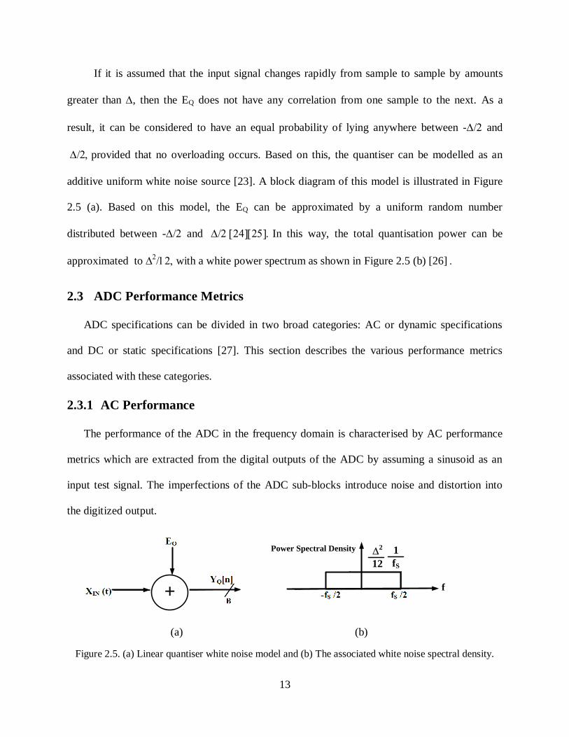
If it is assumed that the input signal changes rapidly from sample to sample by amounts
greater than , then the EQ does not have any correlation from one sample to the next. As a
result, it can be considered to have an equal probability of lying anywhere between - and
provided that no overloading occurs. Based on this, the quantiser can be modelled as an
additive uniform white noise source [23]. A block diagram of this model is illustrated in Figure
2.5 (a). Based on this model, the EQ can be approximated by a uniform random number
distributed between - and In this way, the total quantisation power can be
approximated to with a white power spectrum as shown in Figure 2.5 (b) [26]
2.3 ADC Performance Metrics
ADC specifications can be divided in two broad categories: AC or dynamic specifications
and DC or static specifications [27]. This section describes the various performance metrics
associated with these categories.
2.3.1 AC Performance
The performance of the ADC in the frequency domain is characterised by AC performance
metrics which are extracted from the digital outputs of the ADC by assuming a sinusoid as an
input test signal. The imperfections of the ADC sub-blocks introduce noise and distortion into
the digitized output.
+
Power Spectral Density
f
2
12 fS
1
(a) (b)
Figure 2.5. (a) Linear quantiser white noise model and (b) The associated white noise spectral density.

14
Thereby these metrics indicate the accuracy, noise and distortion of the digitized output.
Important AC specifications include signal-to-noise ratio (SNR), signal-to-noise-and-distortion
ratio (SNDR), dynamic range (DR) and effective number of bits (ENOB). All these
specifications are briefly described in the following while a graphical illustration of these metrics
versus input sinusoid amplitude is given in Figure 2.6 [28].
2.3.1.1 Signal to Noise Ratio
SNR is the ratio of the power at the frequency of an input sinusoid to the total in-band-
noise power at the output of the ADC (in dBs) for specific input amplitude [1][28]. This
parameter is also expressed in VRMS, or %. SNR accounts for the linear performance of the ADC
and therefore in-band-noise associated with harmonics is not included. For an ideal ADC having
input sinusoid amplitude of “X” and considering the quantisation noise of PQ, the SNR is
represented as:
. (2.1)
SNRPEAK
SNDRPEAK
0 XFS/2Input Level
XOL
XOL=Overload Level of Input
XFS=Full scale of Input
Figure 2.6. AC performance metrics on a typical SNR curve of a M ADC [28].
Q
2
102P
X10logSNR

15
2.3.1.2 Signal to Noise plus Distortion Ratio
SNDR is the ratio of the input signal power and the in band noise power while taking into
account the harmonics at the ADC output as well [1]. The magnitude is typically expressed in
dBs. Figure 2.6 illustrates a typical SNDR curve of a M. For the larger input amplitudes, the
curve deviates from the SNR due to the distortions. SNDR is usually calculated for fIN < BW/3,
where fIN is the frequency of input sinusoid and BW is the bandwidth, so that second and third
harmonics lie within the band of interest [28].
2.3.1.3 Dynamic Range
DR is the ratio of the output power of a sinusoid having maximum amplitude to the
output power of the minimum detectable input signal for which SNR=0 dBs [28]. The maximum
amplitude of the input signal can be characterised as peak-to-peak, zero-to-peak or root mean
square (rms). The minimum detectable signal is the rms noise measured with no applied signal.
For a sinusoidal input signal with maximum amplitude at the ADC input XFS/2 having
quantisation noise of PQ, the DR can be represented as:
. (2.2)
2.3.1.4 Effective Number of Bits
The DR of an ADC is reduced due to noise, distortion and other non-idealities present. A
given input cannot be resolved beyond a certain number of bits of resolution, which is known as
effective number of bits (ENOB) [28]. ENOB can be represented as:
. (2.3)
Q
2
FS
102P
2X
10logDR
6.02
1.76DRENOB
dB
16
For M ADCs, instead of a DR in (2.3), SNDRPEAK is used [28].
2.3.1.5 Overload Level
In the context of M ADCs, OL is another important AC performance metric. As
illustrated in Figure 2.6, the SNR of the ADC starts dropping for input amplitudes close to half
of the full scale of input. In that sense, it is considered as the maximum input amplitude for
which the ADC can function correctly.
2.3.2 DC Performance
The DC specifications of the ADC give the performance measures of ADC with steady
state analog inputs. These specifications are more important in instrumentation and measurement
applications such as temperature, pressure or weight etc. In such applications, ADC input signals
are located near DC and possess very low bandwidths. Important DC specifications include
DNL, INL, gain error and offset.
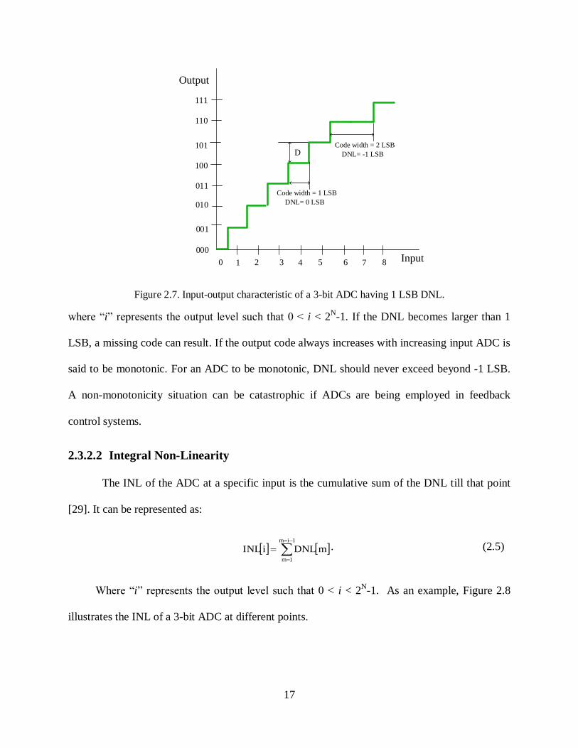
2.3.2.1 Differential Non-Linearity
The output of an ADC is represented in bits, whereby the difference between two
consecutive output levels is equal to one least significant bit (LSB). DNL is the deviation of
difference of two consecutive output levels from the ideal difference (one LSB) [29]. Due to
non-idealities of the ADC, it can be higher than 1 LSB. As an example, Figure 2.7 illustrates the
input-output characteristic of a 3-bit ADC having a DNL of 1 LSB. For an N-bit ADC, DNL can
be represented as:
1LSB
VViDNL i1i
. (2.4)
17
Figure 2.7. Input-output characteristic of a 3-bit ADC having 1 LSB DNL.
where “i” represents the output level such that 0 < i < 2N-1. If the DNL becomes larger than 1
LSB, a missing code can result. If the output code always increases with increasing input ADC is
said to be monotonic. For an ADC to be monotonic, DNL should never exceed beyond -1 LSB.
A non-monotonicity situation can be catastrophic if ADCs are being employed in feedback
control systems.
2.3.2.2 Integral Non-Linearity
The INL of the ADC at a specific input is the cumulative sum of the DNL till that point
[29]. It can be represented as:
1im
1m
mDNLiINL . (2.5)
Where “i” represents the output level such that 0 < i < 2N-1. As an example, Figure 2.8
illustrates the INL of a 3-bit ADC at different points.
0 1 2 Input
Output
D
3 4 5 6 7 8
000
001
010
011
100
101
110
111
DNL= -1 LSB
Code width = 2 LSB
DNL= 0 LSB
Code width = 1 LSB

18
Figure 2.8. Input-output characteristic of a 3-bit ADC with INL, shown as cumulative sum of DNL.
Larger INL not only degrades the DC performance of the ADC, but in addition adds
noise and distortion in the digitized signal, thus degrading the SNR. Therefore, the total amount
of noise at the output of an ADC is the sum of quantisation noise and the noise introduced due to
INL and can be represented as [30]:
.
(2.6)
2.3.2.3 Offset
The transfer function (TF) of an ADC is the relationship of the input to the ADC versus
the code‟s output by the ADC. Offset error shifts the TF curve of the ADC linearly, as illustrated
in Figure 2.9. The magnitude of offset error is equal to the difference between ideal start points
(0.5 LSB) to actual start point [31]. As an example, Figure 2.9 (a) and (b) illustrates the input-
output characteristic of a 3-bit ADC having positive and negative offset, respectively.
0 1 2 Input
Output
D
3 4 5 6 7 8
000
001
010
011
100
101
110
111
DNL = -0.5 LSB
INL = -0.5 LSB
DNL= -0.5 LSB
INL = -1LSB
DNL= -0.5 LSB
INL = -1.5 LSB
NoiseINL
INL12
Δ
12
ΔV
12
0i
2
i
222
noise
N

19
(a) (b)
Figure 2.9. Input-output characteristic of a 3-bit ADC having (a) Positive offset (b) Negative offset.
Offset in an ADC is typically caused due to mismatches of the circuit components
(transistors, capacitors, resistors etc.) and can move with ageing. Depending upon the
application, different strategies can be adopted to remove the offset errors [32][33].
2.3.2.4 Gain Error
Gain error, also known as full scale error is the difference between the full scale output
code and the actual value of the input providing full scale at the output [31]. Although important,
this error can be removed from the digital output. The gain error of an ADC is characterised after
calibrating the ADC readings for the offset.
As an example, Figure 2.10 illustrates the input-output characteristic of a 3-bit ADC
having positive and negative gain errors, respectively. Note that the gain error impacts the
maximum input signal.
0 1 2 Input
Output
3 4 5 6 7 8000
001
010
011
100
101
110
111
Ideal ADC
ADC with positive
offset
0 1 2 Input
Output
3 4 5 6 7 8000
001
010
011
100
101
110
111
Ideal ADC
ADC with negative offset

20
Figure 2.10. Input-output characteristic of a 3-bit ADC with positive and negative gain error.
2.4 Nyquist-rate ADCs
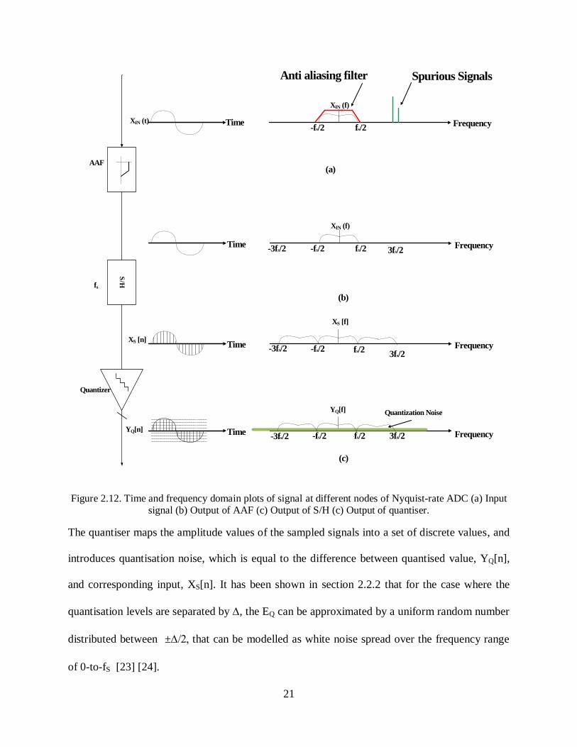
Nyquist-rate ADCs sample at twice the BW of input signals [27]. A block diagram of a
Nyquist-rate ADC along with different sub-blocks is shown in Figure 2.11 while Figure 2.12
illustrates the time and frequency plot of the signal at the inputs and outputs of different sub-
blocks of the ADC. The input signal X(t), after passing through the AAF, is sampled by the S/H
and then passes through the quantiser. Sampling the input signal does not introduce any error in
the signal spectrum, provided the Nyquist criteria are fulfilled.
S/HXIN (t)
XS [n]
Antialiasing Filter
YQ [n]
QuantiserfS
Nyquist Rate ADC
Figure 2.11. Arrangement of blocks in a Nyquist ADC.
0 1 2 Input
Output
3 4 5 6 7 8
000
001
010
011
100
101
110
111
Ideal ADC
ADC with positive gain error
ADC with negative gain error
21
Quantizer
S/H
XIN (t)
XS [n]
YQ[n]
fs
YQ[f]
XS [f]
XIN (f)
Quantization Noise
3fs/2
3fs/2
3fs/2-fs/2
-fs/2
Frequency
XIN (f)
fs/2
-3fs/2
-fs/2
fs/2-fs/2-3fs/2
fs/2
-3fs/2 -fs/2
Anti aliasing filter Spurious Signals
AAF
Frequency
Frequency
Frequency
Time
Time
Time
Time
(a)
(b)
(c)
Figure 2.12. Time and frequency domain plots of signal at different nodes of Nyquist-rate ADC (a) Input signal (b) Output of AAF (c) Output of S/H (c) Output of quantiser.
The quantiser maps the amplitude values of the sampled signals into a set of discrete values, and
introduces quantisation noise, which is equal to the difference between quantised value, YQ[n],
and corresponding input, XS[n]. It has been shown in section 2.2.2 that for the case where the
quantisation levels are separated by , the EQ can be approximated by a uniform random number
distributed between ±that can be modelled as white noise spread over the frequency range
of 0-to-fS [23] [24].

22
The noise introduced by the quantiser is dependent upon the resolution (or quantisation
step i.e. ) of the quantiser and is given by 2 [23]. The quantisation noise, PQ, also
determines the signal-to-quantisation-noise ratio (SQNR). If the maximum input amplitude
applied to an N-bit quantiser is in the non-overload region is XFS/2, then its corresponding power
at the ADC output can be approximated as:
(2.8)
Therefore, the SQNR of the ideal ADC or SQNRMAX is given by:
. (2.9)
Here PQ is the quantisation noise and is given by:
12
ΔP
2
Q (2.10)
Employing the expression for POUT and PQ from (2.8) and (2.10) in (2.9) gives,
SQNRMAX|dB= 6.02N+1.76 (2.11)
2.5 Nyquist-rate ADC Architectures
Nyquist ADCs can be realised with various architectures. Each architecture involves
different trade-offs among speed, accuracy, power and area. A brief overview of three of the
most important architectures namely flash, SAR and pipeline ADCs and their trade-offs are
given here.
2.5.1 Flash ADC
Flash ADCs, also known as parallel ADCs, digitize the inputs with the fastest conversion
time. High speed of such ADCs comes at the cost of the number of comparators employed, as
2N-1 comparators are required for an N-bit flash ADC [27]. A block level diagram of a 2-bit
232N
2N2
FSOUT Δ2
2
Δ/22
2
/2XP
Q
OUT
MAXP
PSQNR

23
flash ADC is shown in Figure 2.13. It consists of a resistor ladder that generates the appropriate
reference voltages, comparator array and a thermometer-to-binary encoder. The comparator-
array compares the input voltage against the reference voltages generated by the resistor ladder.
Digital circuitry at the output of the comparator array maps the thermometric output to binary.
All the comparators work in parallel and thus the conversion is completed in one conversion
cycle.
Flash ADCs have the highest data rate of all ADCs, but the number of comparators,
power and area increase exponentially with the number of bits. Also the matching requirements
of the comparators are another limitation in achieving medium to higher resolution [27].
Figure 2.13. Flash ADC.
Vref Vin
Resistance Ladder Comparators Binary-to-Thermometric
Encoder

24
2.5.2 SAR ADC
The SAR ADC is a preferred architecture for the low power applications as it consists of
only one active block i.e. comparator [34]. A simplified block level diagram of SAR ADC is
shown in Figure 2.14, which consists of an S/H, a digital-to-analog converter (DAC),
comparator and digital SAR logic [34] [35].
The SAR ADC operation is as follow:
1) The input signal is sampled with an S/H.
2) The sampled input signal is compared against the different voltages generated from the
DAC. During the first bit trial also known as the most significant bit (MSB) trial, VIN is
compared with the half of the reference voltage (VREF/2).
3) The resultant MSB sets the search region for the next bit trial. Based on the binary
search algorithm result, during the second bit trial (MSB-1 bit trial), one quarter of
reference voltage (VREF/4) is either added or subtracted from the previously applied
reference and compared with input.
4) The process is performed for each of the N-bit trials.
Figure 2.14. Basic SAR ADC.
S/HVIN
DAC
SAR Logic
VREF
Output Bits
DAC

25
There are two main limitations associated with the SAR ADC architecture. Firstly, due to
the matching limitations of the current CMOS technologies, achieving resolution higher than 10-
bits in SAR ADC requires extra measures, especially calibration. Secondly, this ADC works in a
sequential manner resulting in lower speed compared to their flash counterparts [27]. Using
various techniques (such as time interleaving), the speed of SAR ADCs can be increased but at
the cost of design complexity [36].
2.5.3 Pipeline ADC
A pipeline ADC employs a cascade of low-resolution ADCs to achieve the higher
resolutions as shown in Figure 2.15. It consists of multiple coarse-ADCs arranged in series. Each
coarse-ADC consists of three major blocks: a sub ADC, a DAC, and a residue amplifier.
The ADC functions in a sequential way. As shown in Figure 2.15, input voltage is applied to
the first stage that generates a digital output. This digital output is then subtracted from the input
signal using the DAC generating a residue signal. This residue or error signal is passed through
an amplifier before being fed as the input signal into the next stage. The remaining stages operate
in a similar manner. The digitized outputs from all the stages are combined using a digital block
to generate the final output [37].
Figure 2.15. Pipeline ADC

26
These types of ADCs are suitable for achieving higher resolutions with smaller number of
comparators than flash ADCs. The major drawbacks of these ADCs are latency and higher
power consumption.
2.5.4 Limitations of Nyquist-rate ADCs
One of the important limitations of Nyquist rate architectures is that the circuitry required
and hence power and area consumption, increases for every additional bit of resolution. Also,
due to the matching limitations of the different components in the CMOS process, attaining a
resolution higher than 10-bits in some architectures like SAR, flash etc. require additional
measures like calibration, segmentation etc. [27][38] . Hence, these architectures are typically
limited to low and medium resolution applications.
2.6 Oversampled ADCs
Oversampled ADCs employ a sampling rate i.e. fS, much higher than the Nyquist rate.
Two advantages of such ADCs compared to Nyquist-rate ADCs are the relaxed specifications of
AAF and lower quantisation noise and enhanced resolution.
The ratio of fS and Nyquist-rate in such ADCs is known as oversampling ratio (OSR) and
is given as:
. (2.12)
It was previously stated in section 2.2.2 that the quantiser maps the sampled input to a
discrete set of values and introduces quantisation noise with power equal to If
fSis increased above Nyquist frequency, the quantisation noise power remains the same but now
it is distributed over the wider frequency range and hence the in-band noise is reduced by the
same ratio.
BW2
fOSR S

27
Figure 2.16 (a) and (b) illustrates the Nyquist-rate and oversampled ADCs along with
their power spectral density (PSD) of quantisation noise, respectively. Oversampled ADCs are
typically followed by a LP filter and down-sampler which is commonly referred as the
decimation filter.
The quantisation noise in the band of interest is given by:
(2.13)
Applying the same procedure as described in section 2.4, the SQNRMAX can be calculated as
follow:
. (2.14)
. (2.15)
In other words, oversampling by a factor of 4, increases the SQNRMAX, by 6 dB or one bit.
frequency
(a) (b)
Figure 2.16.Quantisation noise of (a) Nyquist-rate ADC (b) Oversampled ADC.
OSR 12
ΔP
2
Q
OSR2
2
3
/2Δ
OSRΔ/22
P
PSQNR 2N
2
2N
Q
OUTMAX
dBOSR10log1.766.02NSQNR 10MAX
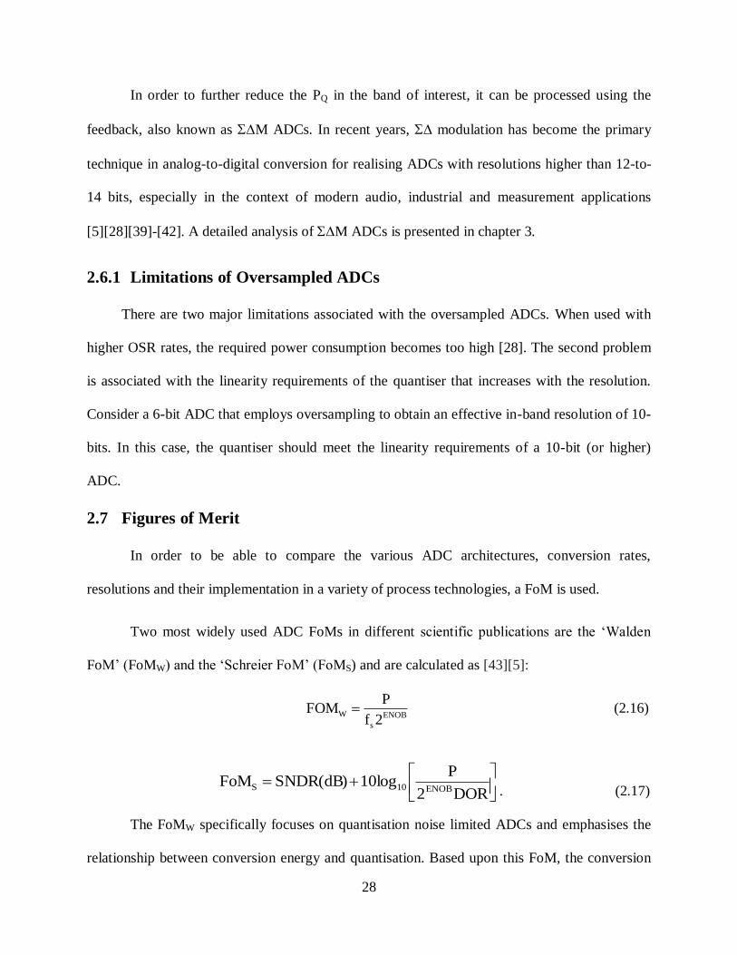
28
In order to further reduce the PQ in the band of interest, it can be processed using the
feedback, also known as M ADCs. In recent years, modulation has become the primary
technique in analog-to-digital conversion for realising ADCs with resolutions higher than 12-to-
14 bits, especially in the context of modern audio, industrial and measurement applications
[5][28][39]-[42]. A detailed analysis of M ADCs is presented in chapter 3.
2.6.1 Limitations of Oversampled ADCs
There are two major limitations associated with the oversampled ADCs. When used with
higher OSR rates, the required power consumption becomes too high [28]. The second problem
is associated with the linearity requirements of the quantiser that increases with the resolution.
Consider a 6-bit ADC that employs oversampling to obtain an effective in-band resolution of 10-
bits. In this case, the quantiser should meet the linearity requirements of a 10-bit (or higher)
ADC.
2.7 Figures of Merit
In order to be able to compare the various ADC architectures, conversion rates,
resolutions and their implementation in a variety of process technologies, a FoM is used.
Two most widely used ADC FoMs in different scientific publications are the „Walden
FoM‟ (FoMW) and the „Schreier FoM‟ (FoMS) and are calculated as [43][5]:
ENOB
s
W2f
PFOM (2.16)
. (2.17)
The FoMW specifically focuses on quantisation noise limited ADCs and emphasises the
relationship between conversion energy and quantisation. Based upon this FoM, the conversion
DOR2
P10logSNDR(dB)FoM
ENOB10S

29
energy increases by a factor of two when doubling the conversion accuracy (6dBs in SNDR or
one extra ENOB). Therefore, a lower FoMW means a more power efficient ADC. On the other
hand, the FoMS specifically addresses thermal noise limited designs. It reflects that to reduce the
in-band thermal noise by 50%, the resultant energy consumption increases by a factor of four.
Therefore, a better ADC is characterised by a higher FoMS. Figure 2.17 and Figure 2.18 illustrate
the FoMW and FoMS of the different ADCs reported in different scientific publications over the
years [5]. These two figures show the historical progress in ADC performance with a focus
on energy per sample, SNDR and speed. The dotted lines in the figure show the implicit
performance barriers. Over the years, a significant improvement in the ADC performance can be
observed.
Figure 2.17. FoMW versus DOR for different ADCs published in VLSI and ISSCC [5].
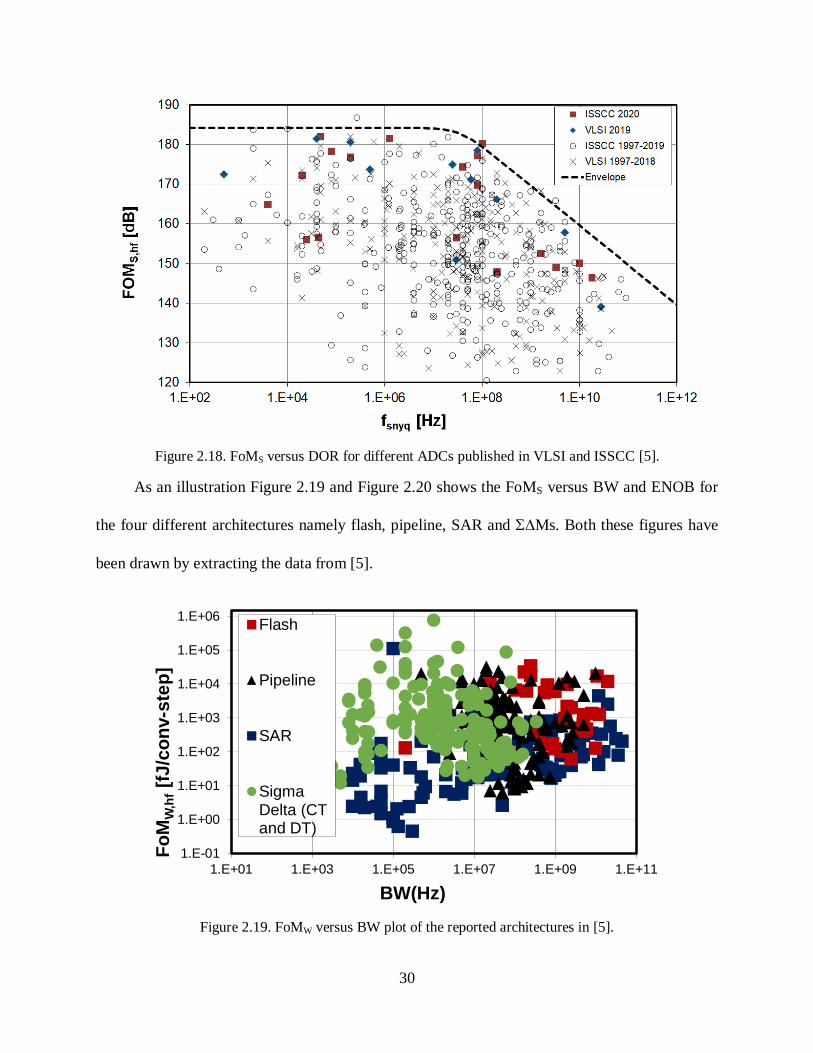
30
Figure 2.18. FoMS versus DOR for different ADCs published in VLSI and ISSCC [5].
As an illustration Figure 2.19 and Figure 2.20 shows the FoMS versus BW and ENOB for
the four different architectures namely flash, pipeline, SAR and Ms. Both these figures have
been drawn by extracting the data from [5].
Figure 2.19. FoMW versus BW plot of the reported architectures in [5].
1.E-01
1.E+00
1.E+01
1.E+02
1.E+03
1.E+04
1.E+05
1.E+06
1.E+01 1.E+03 1.E+05 1.E+07 1.E+09 1.E+11
Fo
MW
,hf [f
J/c
on
v-s
tep
]
BW(Hz)
Flash
Pipeline
SAR
SigmaDelta (CTand DT)
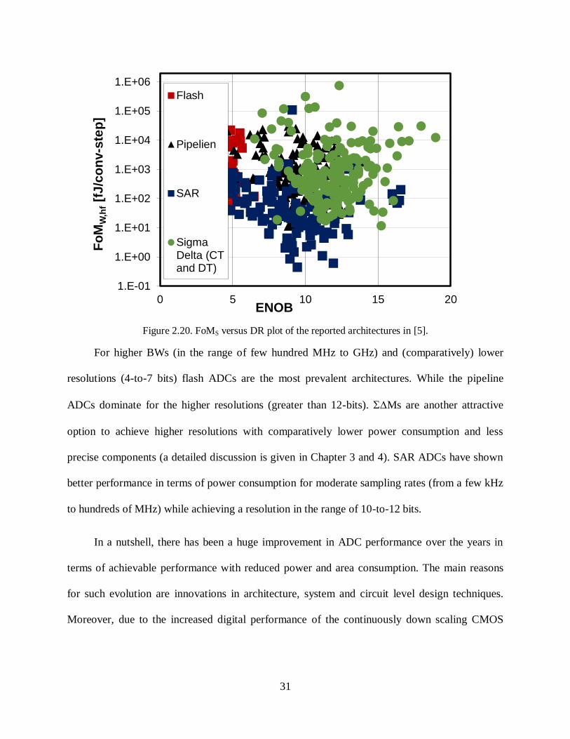
31
Figure 2.20. FoMS versus DR plot of the reported architectures in [5].
For higher BWs (in the range of few hundred MHz to GHz) and (comparatively) lower
resolutions (4-to-7 bits) flash ADCs are the most prevalent architectures. While the pipeline
ADCs dominate for the higher resolutions (greater than 12-bits). Ms are another attractive
option to achieve higher resolutions with comparatively lower power consumption and less
precise components (a detailed discussion is given in Chapter 3 and 4). SAR ADCs have shown
better performance in terms of power consumption for moderate sampling rates (from a few kHz
to hundreds of MHz) while achieving a resolution in the range of 10-to-12 bits.
In a nutshell, there has been a huge improvement in ADC performance over the years in
terms of achievable performance with reduced power and area consumption. The main reasons
for such evolution are innovations in architecture, system and circuit level design techniques.
Moreover, due to the increased digital performance of the continuously down scaling CMOS
1.E-01
1.E+00
1.E+01
1.E+02
1.E+03
1.E+04
1.E+05
1.E+06
0 5 10 15 20
Fo
MW
,hf [f
J/c
on
v-s
tep
]
ENOB
Flash
Pipelien
SAR
SigmaDelta (CTand DT)

32
technologies, digitally assisted analog components can achieve higher precision. This fact has
also benefitted the ADCs.
Another interesting fact observed from [5] is that there has been a surge in hybrid-type
architectures e.g. noise shaping SAR ADCs or replacing the internal quantiser of a M with a
SAR ADC. Moreover, time-based quantisers along with digital-assisted analog circuits have also
been increasingly used to get better resolution with lower power and area consumption [5].
2.8 Conclusion
The basic principles of sampling and quantisation have been presented in this chapter. A
few of the important performance metrics have also been described briefly. In addition, two
important types of ADCs namely Nyquist-rate ADCs and oversampling ADCs along with their
limitations have also been examined. Finally, two important FoMs have been discussed. These
FoMs are very useful when comparing different ADC implementations.
Two types of the ADCs highlighted in this chapter, have different applications. On one end,
Nyquist-rate ADCs, specifically SAR ADCs can achieve medium to high resolution in modern
CMOS technologies with moderate or low power consumption while one the other end the M
ADCs are better suited for much higher resolution applications. In the following chapters,
architectural level exploration, modelling, design, implementation and experimental
characterization of both types of these ADCs for two important application areas i.e. wireless
communication and PMICs are given.

33
Chapter 3: M ADCs
3.1 Introduction
It has been discussed in the previous chapter that oversampling improves the achievable
performance of ADCs. The maximum achievable SQNR of an N-bit ADC when oversampled by
a factor of OSR, is given as:
OSR10log1.766.02NSQNR 10MAX (3.1)
Equation (3.1) demonstrates that increasing the OSR by a factor of 4 yields one additional bit (6
dB) in resolution. The sole dependence on OSR to achieve the higher resolution ADC results in
prohibitively large sampling rates. Oversampling combined with modulation (M) is an
effective way of obtaining higher resolution. In these ADCs, the quantisation noise is suppressed
in the signal band by the noise shaping and hence for a given OSR, better resolution is achieved.
In recent years, modulation has become an important technique in analog-to-digital
conversion for realising ADCs with a resolution higher than 12-bits, especially in the context of
modern audio, industrial and measurement applications [5][12]-[19][27][28][39]-[42]. First
introduced in 1962 [46], the use of such types of ADC gained importance with the advancements
in CMOS processes. In current system-on-chip designs, a major portion of the silicon CMOS die
consists of digital logic. As ADCs are based on the signal processing techniques (noise
shaping), these ADCs are more suited for such applications [47]. M ADCs can achieve higher
resolutions with comparatively low-resolution analog circuits compared to their Nyquist rate
counterparts [28]. Moreover, these ADCs impose lower requirements in terms of matching and
tolerance for the different analog and mixed signals blocks e.g. comparators and op-amps used

34
[27]. These advantages have resulted in an increased interest in the design of ADCs [12]-
[14][27][28][39]-[42][45].
This chapter introduces the basic concepts and different implementation alternatives for
ADCs. The outline of this chapter is as follows. Section 3.2 presents the principles of noise
shaping and ADCs. Different topologies such as single-loop first and second-order
modulator, single loop higher order and multiple loop or cascaded are also described in the same
section. Multibit converters are addressed in section 3.3. Section 3.4 details the BP-ADC
while continuous time implementations of ADC and time-encoded quantiser based
ADC are discussed in sections 3.5 and 3.6, respectively.
3.2 Working Principle ofM ADCs
Oversampled ADCs combined with feedback result in quantisation noise shaping that
reduces the error in the band of interest [45][46]. Feedback has long since been used in electrical
systems for error reduction [48]. If the forward path gain is high enough, the average value of the
feedback path approaches the input and hence the quantisation noise is reduced. A basic
configuration of M ADC is shown in Figure 3.1 (a) and (b), where X(z), Y(z) and E(z)
represent the input signal, the output and quantisation noise of the modulator, respectively. The
forward path consists of a filter H(z) with higher gain in the band of interest and a quantiser. Due
to the negative feedback, “Y(z)” is subtracted from the input X(z). The difference between these
two signals is frequency weighed with the loop filter H(z). The input signal is passed to the
output without attenuation while the difference is attenuated by the filter. The resultant output
from the filter is passed to the quantiser that generates the next output i.e. “Y(z)”. This output is
again fed back to the input summing node for the next comparison. As a result of this strategy,

35
most of the error (or quantisation noise) is suppressed in the signal band and pushed towards
higher frequencies [28].
A linearized form of this model is shown Figure 3.1 (b), where the quantiser has been
replaced with a white noise model (as described in chapter 2). Therefore, the ADC can be
considered to have two inputs i.e. an input signal, X(z), and quantisation noise source, E(z), and
one output, Y(z). The output of the ADC can be written as:
E(z)Y(z)][X(z)H(z)Y(z) . (3.2)
Where H(z) is the loop filter TF. Hence, (3.2) can be rearranged as:
E(z)
H(z)1
1X(z)
(z)H1
H(z)zY
. (3.3)
E(z)NTFX(z)STFzY . (3.4)
H(z)X(z)
Y[z]
DAC
Quantizer
H(z)
X(z)
DAC
k
E(z)
(a)
(b)
Y[z]
Figure 3.1. (a) A basic ADC (b) Linearised model of ADC.

36
Where the signal transfer function (STF) and the noise transfer function (NTF) are respectively
given by:
H(z)1
H(z)STF
(3.5)
H(z)1
1NTF
. (3.6)
If the H(z) has a high gain at low frequencies, the STF approaches unity. Therefore, the
output signal is an accurate representation of the input signal. Contrary to this, the NTF behaves
as a high-pass (HP) filter and thus blocks the quantisation noise at the lower frequencies, shaping
the quantisation noise away from the lower frequencies, where the input signal resides thus
extending the achievable SQNR.
The concept of the noise shaping can be easily extended to BP signals, resulting in noise
shaping the quantisation noise away from the band-of-interest, now centred at a frequency other
than DC, which is also referred as BP M. This will be explained in the following sections.
Over the years, several ADCs have been proposed [5][12]-[19][27][28][39]-[42].
Starting from a simple first-order modulator, various implementation alternatives are briefly
described in the following sections.
3.2.1 First-order LP M
A first-order LP modulator is shown in Figure 3.2. The forward path of the modulator
consists of a single discrete time LP filter H(z). The TF of the integrator is given by:
1
1
z1
zH(z)
(3.7)
Considering Figure 3.2 and employing the relationship given in (3.3), output of the first-order
M is given by:

37
E(z)z1X(z)zY(z) 11
. (3.8)
Therefore, NTF and STF become:
1z1E(z)
Y(z)NTF , (3.9)
1zX(z)
Y(z)STF . (3.10)
The STF in equation (3.10) signifies that the input signal is passed to the output with a
single delay, while the NTF (equation (3.9)) indicates that the quantisation noise is differentiated
by the modulator loop. The differentiator signifies a HP function, thus shaping the quantisation
noise away from the lower frequencies and towards higher frequencies.
As an example, a sinusoidal input signal having a frequency of 31 kHz has been digitized
at a sampling rate of 128 MHz (OSR=2048). The output spectrum of the ADC is shown in
Figure 3.3, depicting the noise shaping with a slope of 20 dB/dec. It is evident that the
quantisation noise is no longer flat and is shaped out of the band of interest into the higher
frequencies.
H(z)X(z)
DAC
Y(z)
Figure 3.2. First-order M.

38
Figure 3.3. Magnitude spectrum of a first-order M depicting a noise shaping with a slope of 20 dB/dec.
The in-band quantisation noise of a first-order M ADC for a given OSR and single bit
quantiser can be approximated as [28][49]:
12
Δ
OSR
1
3
πP
2
3
2
Q (3.11)
SQNRMAX of an ADC is the ratio of full-scale input and the quantisation noise and is given by:
Q
X
MAX
P
SSQNR
(3.12)
Where, SX =Full-scale input (3.13)
2
X
22
1S
(3.14)
Using (3.11-3.14), the SQNRMAX (in dBs) of first-order M ADC can be written as:
2
3
10MAXπ
OSR
2
910logQNRS (3.15)
The above expression shows that doubling the OSR, increases the SQNRMAX by 9 dB compared
to 3 dB improvement using oversampling alone.
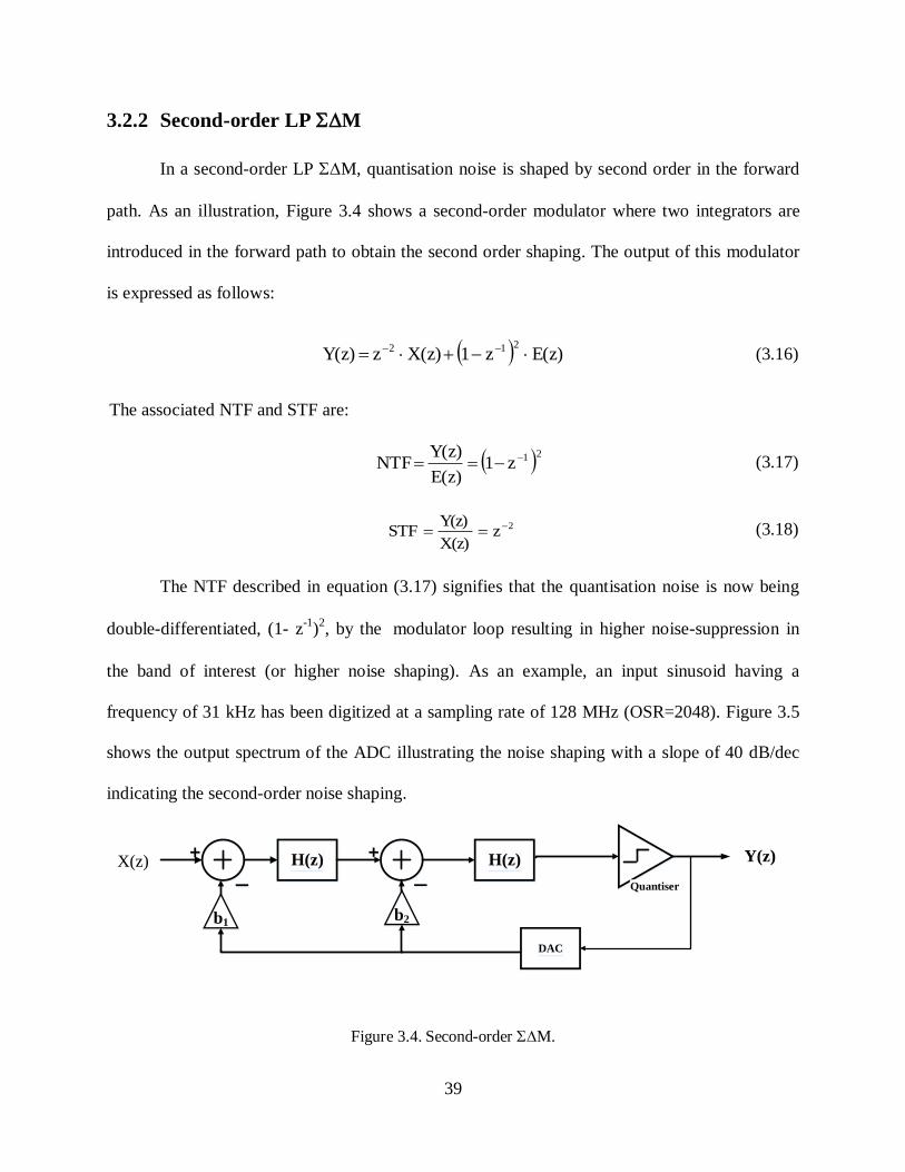
39
3.2.2 Second-order LP M
In a second-order LP M, quantisation noise is shaped by second order in the forward
path. As an illustration, Figure 3.4 shows a second-order modulator where two integrators are
introduced in the forward path to obtain the second order shaping. The output of this modulator
is expressed as follows:
E(z)z1X(z)zY(z)212
(3.16)
The associated NTF and STF are:
21z1E(z)
Y(z)NTF (3.17)
2zX(z)
Y(z)STF (3.18)
The NTF described in equation (3.17) signifies that the quantisation noise is now being
double-differentiated, (1- z-1
)2, by the modulator loop resulting in higher noise-suppression in
the band of interest (or higher noise shaping). As an example, an input sinusoid having a
frequency of 31 kHz has been digitized at a sampling rate of 128 MHz (OSR=2048). Figure 3.5
shows the output spectrum of the ADC illustrating the noise shaping with a slope of 40 dB/dec
indicating the second-order noise shaping.
Quantiser
H(z)X(z)
DAC
H(z)
b1b2
Y(z)
Figure 3.4. Second-order M.

40
Figure 3.5. Magnitude spectrum of a second-order M depicting noise shaping with a slope of 40
dB/dec.
The quantisation noise and the SQNRMAX of a second-order M ADC for a given OSR
and single bit quantiser can be approximated as [28][49]:
12
Δ
OSR
1
5
πP
2
5
4
Q . (3.19)
Using expressions for SX from (3.13) and PQ from (3.19), the SQNRMAX (in dBs) is given by:
4MAX π2
4OSR 15
1010logSQNR . (3.20)
Equation (3.20) shows that doubling the OSR increases the SQNRMAX by 15 dB compared to 9
dB improvement of first-order M ADC.
3.2.3 Higher Order M ADC
In order to suppress the quantisation noise more effectively at targeted frequencies,
additional filtering stages can be introduced in the forward path. As an example, a higher order
M consisting of “L” integrators is depicted in Figure 3.6. Using (3.3)-(3.6), output of
modulator i.e. Y(z), NTF and STF of M can be written as:

41
E(z)z1X(z)zzYL1L (3.21)
L1z1E(z)
Y(z)NTF (3.22)
Lz
X(z)
Y(z)STF (3.23)
Considering a single-bit quantiser having order L, the quantisation noise and SQNRMAX
for a given OSR can be approximated as:
12
Δ
OSR
1
12L
πP
2
1)(2L
2L
Q , (3.24)
2LMAX
π2
1)(2LOSR 1L 2 3
1010logSQNR . (3.25)
The achievable SQNRMAX with an order of 0-to-5, over a wide range of OSR values is
depicted in Figure 3.7. It shows that by increasing the loop order, higher noise quantisation
suppression can be achieved at lower frequencies. In reality, the achievable performance for a
higher order loop filter (L > 2) is far less than shown in Figure 3.7 due to the stability issues [50].
Unlike the first and second-order single bit modulators, the out-of-band gain (OBG) increases
significantly for the higher order modulators. As a result, internal states of the modulator or the
integrator outputs and quantiser input saturate more easily.
Quantiser
H(z)X(z)
DAC
H(z)
b1b2
Y(z)H(z)
b3
Figure 3.6. A higher order M.

42
Figure 3.7. Achievable SQNRMAX of a M ADC over a wide range of OSR and order.
Furthermore, larger input signals can produce low frequency, high amplitude limit cycles at the
input of the quantiser [44][45][50]. These cycles are difficult to predict with the commonly used
quantiser model. Different measures can be adopted to cater to stability issues. The loop filter
coefficients can be scaled to keep the OBG lower. Two other measures include limiting the input
signal range and the use of a multibit quantiser [50][51].
3.2.4 Cascaded or Multistage Noise Shaping
As explained in the previous section, an increase in the order of loop filter enhances the
quantisation noise suppression but introduces stability problems. One way to increase the order
while maintaining the stability is the cascading of stable first or/and second-order stages
resulting in a high order stable system as illustrated in Figure 3.8 [52]-[56]. Each stage in the
modulator processes the quantisation noise from the preceding stage while the outputs of all the
stages are combined in digital domain, in a way that quantisation noise of all the stages gets
cancelled, except the quantisation noise from the last stage [44][54][55]. The final output
available from the digital block (known as digital cancellation logic (DCL)), has the quantisation
noise shaping equal to the sum of orders of all the cascaded stages.

43
As ADCs with L>2 are not unconditionally stable, only first and second-order single
loops are typically used. As an example, a 1-1-1 cascaded M is shown in Figure 3.8. In order
to analyse the noise shaping, consider the quantisation noise introduced by three stages are E1(z),
E2(z) and E3(z). Using the linearised model, output of the modulator can be written as follow:
zEz1zXzzY313 . (3.26)
If the error cancellation functions are chosen below,
21
3
1
12
1
2
1
1
z1zH
,z(z)H
,z1zH
,z(z)H
(3.27)
H(z)
X (z)
DAC
H1 (z)
H(z)
DAC
H2 (z)
H3 (z)
H12 (z)
Y
DCL
H(z)
DAC
Figure 3.8. A 1-1-1 cascaded M.
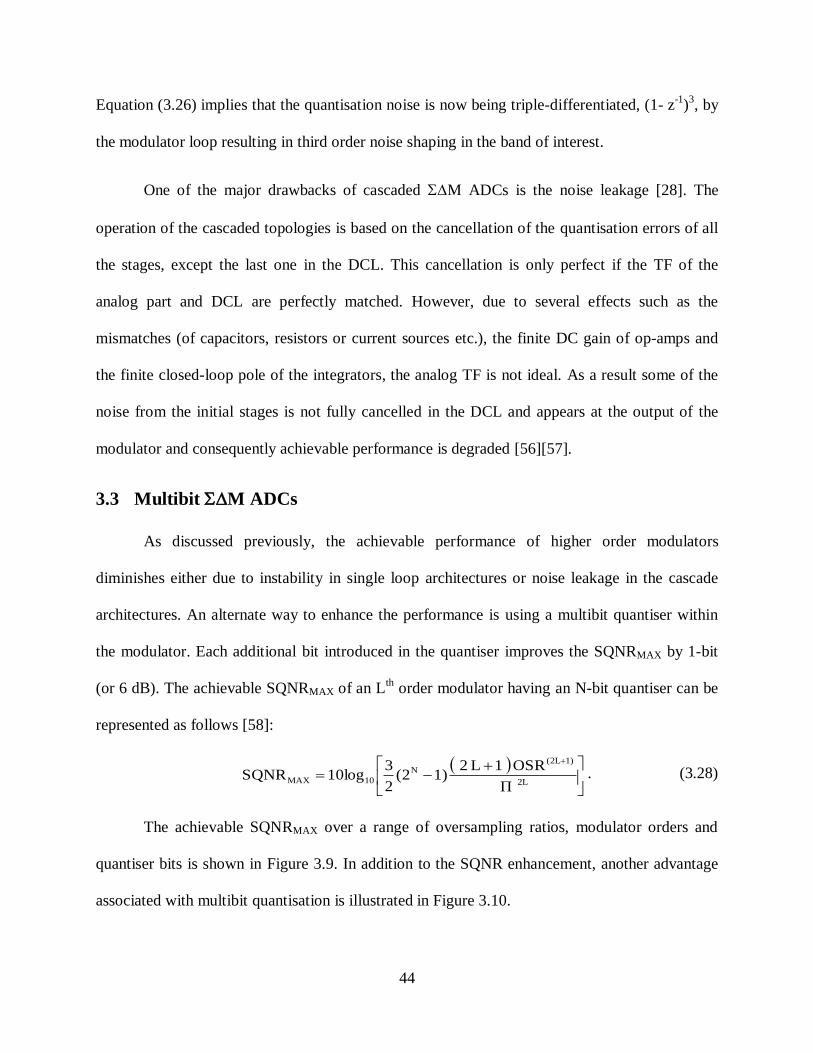
44
Equation (3.26) implies that the quantisation noise is now being triple-differentiated, (1- z-1
)3, by
the modulator loop resulting in third order noise shaping in the band of interest.
One of the major drawbacks of cascaded M ADCs is the noise leakage [28]. The
operation of the cascaded topologies is based on the cancellation of the quantisation errors of all
the stages, except the last one in the DCL. This cancellation is only perfect if the TF of the
analog part and DCL are perfectly matched. However, due to several effects such as the
mismatches (of capacitors, resistors or current sources etc.), the finite DC gain of op-amps and
the finite closed-loop pole of the integrators, the analog TF is not ideal. As a result some of the
noise from the initial stages is not fully cancelled in the DCL and appears at the output of the
modulator and consequently achievable performance is degraded [56][57].
3.3 Multibit M ADCs
As discussed previously, the achievable performance of higher order modulators
diminishes either due to instability in single loop architectures or noise leakage in the cascade
architectures. An alternate way to enhance the performance is using a multibit quantiser within
the modulator. Each additional bit introduced in the quantiser improves the SQNRMAX by 1-bit
(or 6 dB). The achievable SQNRMAX of an Lth
order modulator having an N-bit quantiser can be
represented as follows [58]:
2L
1)(2LN
10MAX Π
OSR 1L 2 1)(2
2
310logSQNR . (3.28)
The achievable SQNRMAX over a range of oversampling ratios, modulator orders and
quantiser bits is shown in Figure 3.9. In addition to the SQNR enhancement, another advantage
associated with multibit quantisation is illustrated in Figure 3.10.

45
Figure 3.9. Achievable SQNRMAX over a range of OSR, order and quantiser bits.
Am
pli
tud
e (V
)
Output Samples (Number)
Figure 3.10. Input and output of first-order of M ADC having multibit quantiser.
The output of such modulators follows the input more closely than their single bit
counterparts. Therefore, the output swing requirements of the integrators are reduced. As a
result, the slew-rate requirements and the power consumption are reduced [59]. There are two
major limitations associated with multibit quantisers, which are typically implemented as a flash
ADC. Firstly, the circuit complexity increases with each additional bit. Second limitation is
related to the non-linearity due to mismatches in multibit feedback DAC [58]. A detailed
analysis of this problem is performed in the following section.
3.3.1.1 DAC Non-linearity
A single-bit DAC has inherent linearity as it consists of a single switched element
(capacitor, current or resistor etc.). Any deviation from its nominal value does not result in a
non-linearity because the single element is switched either positive or negative. Contrary to this,

46
a multibit DAC suffers from non-linearity. Figure 3.11 (a) and (b) illustrate a M ADC with a
multibit quantiser and its associated linearised model. The errors associated with multibit
quantiser and feedback DAC are represented by “EADC” and “EDAC”, respectively. EADC is
introduced in the same path as that of the quantisation error and hence it is attenuated by the loop
filter and suppressed in the signal band. The DAC errors are introduced in the feedback path and
are therefore not shaped. This results in a non-linearity in the modulator. The most commonly
used technique to reduce the impact of DAC non-linearity is called dynamic-element-matching
(DEM) [60]. Using this technique, the one-to-one correspondence between an input code and the
associated DAC error is broken and as a result the in-band distortion is reduced.
Over the years various DEM techniques have been developed [50]. Four major types of
DEM include randomization [61], data weighted averaging (DWA) [62], clocked averaging [63]
and individual level averaging (ILA) [60]. The major limitations of DEM are extra cost in terms
of area and power.
N-bit Quantiser
H(z)XIN (t) Y[z]
N-bit DAC
N-bit Quantiser
H(z)
ke
(a)
(b)
EADC
EDAC
Y[z]
XIN (t)
Figure 3.11. (a) A simple model of M ADC having multibit quantiser and DAC (b) Linearised
model of M ADC with multibit quantiser and DAC.

47
3.4 BP-ADCs
As previously mentioned, ADCs typically have the quantisation noise suppressed at
lower frequency or DC. BP-M ADCs operate on the same principle but suppress the noise at
some higher frequencies [12]-[19][40][64][65]. In the LP architectures, LP filters or integrators
have been employed in the forward path. The TF of an integrator has a pole at DC which
becomes zero of the NTF, hence suppressing the quantisation noise at the lower frequencies. In
BP- ADCs, these integrators are replaced with BP loop filters resulting in an NTF having
zeroes at desired notch frequencies (fN), hence, shaping the quantisation noise away from the
band of interest, into both the higher and lower frequencies. The digital output of the modulator
can be translated to DC by a digital mixer and then digital LP and decimation filters are used to
obtain digital baseband data, subsequently to be processed by the DSP.
3.4.1 Design of BP-M ADCs
The most common way to design the BP filters (also referred as resonators) required in a
BP-Σ∆M is to take the integrators of an already designed LP modulator and to apply a LP-to-BP
transformation. A general LP-to-BP transformation is given as [66]:
1
s
N
1
s
N2
1
zf
f 2π cos 1
zf
f 2π cos z-
z
. (3.29)
Where:
fN = Resonant or notch frequency
and fS= Sampling frequency

48
Using this transformation, the poles of the resonators can be placed anywhere between 0 (i.e. fN
= 0) and π (i.e. fN = fS/2). One of the most important cases is with pole= π/2 or fN=fS/4. For this
particular case, the LP to BP transformation (3.29) reduces to:
1
12
1
z2
cos 1
z2
cos z-
z
, (3.30)
21 -zz . (3.31)
Equation (3.31) results in a BP-Σ∆M ADC that suppresses the quantisation noise around fS/4.
This transformation is illustrated in Figure 3.12 (a) and (b) for a second-order LP-M, which is
mapped to a 4th
-order BP-M. Due to this transformation, the zeros of NTF are mapped to ±
fs/4, reducing the quantisation noise. The achievable resolution and DR of this 4th-order BP-
Σ∆M is the same as the original second-order LP-Σ∆Ms. This is due to the reason that only two
zeros of NTF are located at fS/4, while the other two are located at − fS/4, hence the quantisation
noise is only suppressed with a second-order TF. Moreover, the resulting BP architecture
preserves all performance metrics (SQNRMAX, IBN, stability etc.) of its LP original counterpart.
Figure 3.13 (a) and (b) shows the output spectrum of the LP and BP modulators of Figure 3.12
(a) and (b), respectively.
XIN(z) Y[z]
DAC
0.5z-1
1-z-1
0.5z-1
1-z-1
(a)

49
XIN(z) Y[z]
DAC
-0.5z-2
1-z-1
-0.5z-2
1-z-1
(b)
Figure 3.12 (a) Second-order LP-M ADC (b) Equivalent 4th-order BP-M ADC.
(a)
(b)
Figure 3.13. Spectrum plots of ADCs outputs (a) A second-order LP-M ADC (b) Fourth order BP-
M ADC.
0 0.1 0.2 0.3 0.4 0.5-200
-150
-100
-50
0
Ma
gn
itu
de
(d
B)
Frequency (Hz)
ADC Output
0 0.1 0.2 0.3 0.4 0.5-200
-150
-100
-50
0
Ma
gn
itu
de
(d
B)
Frequency (Hz)
ADC Output

50
One major disadvantage associated with these modulators is the increased complexity
over an equivalent LP modulator.[67][70].
As the BP-Ms can digitize the input signals at higher frequencies, these architectures
are better suited for the direct digitization of the different wireless communication standards
[12]-[19]. This trend has been further fuelled by the faster scaled CMOS technologies,
innovative system level architectures and faster amplifiers [5][28][39][64][65][67][71]. First part
of this thesis focuses on the utilization of the noise shaping capabilities of the BP architectures
for the SDR applications to achieve the desired resolutions over wider bandwidths at higher input
frequencies. In that context, two different architectures of BP-Ms capable of digitizing a wider
range of wireless communication standards have been introduced. An exhaustive analysis of
these modulators is given in chapters 4 and 5.
3.5 Continuous Time M ADCs
The majority of the reported ΣΔM ADCs in the previous 30 years have been implemented
using DT filters, with SC or switched current (SI) techniques as described in [68] and [69],
respectively. The achievable performance of DT-ΣΔMs is limited by settling accuracy of discrete
time integrators and resonators at higher sampling frequencies [70]. More importantly,
incomplete settling of the first integrator is a big design concern since it must settle within the
resolution of the whole ADC within one clock cycle. Therefore, for higher bandwidth
applications, DT-ΣΔMs are not a suitable option. An alternate option is to realise these filters
using continuous time architectures. The performance of CT-M ADCs is not limited by
settling accuracy and hence they can operate at higher sampling frequencies [28][70][71].
A generalised form of CT-M ADC is shown in Figure 3.14 [70][72][73]. This
architecture consists of an AAF, a CT loop filter H(s) along with quantiser and decimation

51
filters. There are some other advantages associated with CT ΣΔMs, as well. Unlike the discrete
time implementation, the sampling operation in CT modulators takes place inside the ΣΔM loop
(at the quantiser). As a result, all of the errors associated with sampling circuit including aliasing
are noise-shaped [70]. Moreover, the loop filter also provides some degree of implicit anti-
aliasing. As a result, specifications of the front end AAF are greatly reduced and in some cases, it
is no longer required. Another advantage of a CT implementation is associated with the input
driving circuitry of the ADC. The input capacitors in DT modulators are kept large enough to
reduce overall thermal noise of the ADC. Such capacitors require larger input buffers resulting in
huge power consumption. Moreover, switching noise introduced by the input circuitries degrades
the achievable performance of the overall digitizing system [70]. On the other hand, due to the
absence of sampling capacitors in CT implementations, complexity of input driving circuitry is
reduced.
Y[z]
X(t) H(s)
DAC
AAF
Digital Filter Downsampler
Figure 3.14. Arrangement of different blocks in a CT-M ADC with AAF.

52
3.5.1 Synthesis of CT-M ADC
A CT modulator can be synthesised from a given DT modulator by means of loop-filter
transformation.The two modulators are equivalent if, for the same input waveform, input to the
quantiser at sampling instants are equal [70]. For this purpose, the modulator loop is opened as
depicted in Figure 3.15(a) and (b) for LP DT-ΣMs and LP CT-ΣMs, respectively.
The transformation can be represented in mathematical form as:
SnTt
11 H(z)z(G(s))L
. (3.32)
where
(s)H(s).HG(s) DAC . (3.33)
Here H(s) and HDAC(s) are the loop and DAC TFs in CT modulators, respectively. The DAC can
take different waveforms and as a result HDAC(s) can vary. The most common DAC architectures
employed are non-return-to-zero (NRZ), return-to-zero (RZ) and half-delayed-return-to-zero
(HRZ) which are depicted in Figure 3.16 and can be expressed as:
Otherwise
Tbta0bta
0
1(t)h
S
DAC
(3.34)
x(t) Y(n)
DAC
H(z)q(n)
y(t)
H(z)DACY(n) u(n)
x(t) Y(n)
DAC
H(s)q(n)
y(t)
HBP(s)Y(n)
HDAC(s)
HDAC(s)
fS
q(n)
fS
G(s)
(a) (b)
Figure 3.15. Loop filter in Ms for (a) DT and (b) CT implementations.

53
In the S-domain, equation (3.34) is given by:
s
e e(s)H
bsas
DAC
. (3.35)
Employing this transformation, the loop filter coefficients for the CT-Ms can be calculated. A
more detailed analysis of the CT design methodology is presented in chapter 4.
3.5.2 Limitations of CT-M ADCs
Two major drawbacks associated with CT-M ADCs are the high sensitivity to clock
jitter and excess loop delay (ELD) in the feedback DAC [70].
In CT modulators, the feedback waveform is integrated over time and thus the modulator
performance is extremely sensitive to every deviation from the exact, ideal waveform of that
feedback signal. Another limitation is associated with the loop filter coefficients which are
realised by an RC or gmC product that can have the mismatches in the range of 20%. As a result
of this, the stability of such modulators becomes a big concern, specifically in higher order
modulators [70] .
Figure 3.16. Rectangular shaped DAC waveform.

54
3.6 Timed-Encoded Quantiser Based M ADCs
Instead of the amplitude, multibit quantiser can also be implemented by using the timing
information of the signal for the digitization. One of the important types of such architectures is a
voltage controlled oscillator (VCO)-quantiser as depicted in Figure 3.17 [54][75]. Here the
quantisation is performed by the voltage-to-frequency conversion. These quantisers typically
consist of an oscillator and a counter that counts the number of edges within a given time period.
The result is directly related to the input signal, thus a digital representation of the input
amplitude is obtained. The major limitation associated with such architectures is the nonlinear
operation of the voltage-to-frequency conversion within the VCO. This problem can be
overcome by using a phase detector instead of a frequency detector, as detailed in [75].
x(t) Y(n)
DAC
Loop
Filter
q(n)
y(t)
VCO-
Quantiser
CLK N-bit Register
Figure 3.17. A VCO-quantiser based M ADC

55
DAC
Loop
Filter
q(n)
y(t)
PWM
Generator
q(n) Time-to-
Digital
Converter
Y(n)x(t)
Figure 3.18. A PWM-quantiser based M ADC
Another alternate to the quantiser is the pulse-width-modulator (PWM) as illustrated in
Figure 3.18 [76]. The PWM converts the voltage into a pulse and then a time-to-digital converter
(TDC) generates the digital representation of the input. The limited DR is one of the important
concerns associated with PWM based quantisers [76].
3.7 Conclusion
The basic operational principles for the oversampled noise shaping M ADCs were
described in this chapter. For resolutions higher than 12-bits, oversampled modulation is a
well-established technique compared to Nyquist rate ADCs. Different implementation
alternatives of M ADCs, including single loop, cascaded, multibit, BP and CT etc. were
briefly described. Finally, time-encoded quantiser based ADCs were also discussed.
Due to high resolution requirements and the latest innovations at architectural-level and
circuit-level design techniques, M ADCs have become an important choice for use in
communication related applications [5][28][39][41][49][52][71]. The next chapter describes a
M suitable for realising an SDR receiver.

56

57
Chapter 4: M Based SDR Receivers
4.1 Introduction
An SDR receiver performs most of the signal processing in the digital domain thus
allowing the programmability and adaptability to ever-emerging wireless communication
standards. In these architectures, as illustrated in Figure 4.1, the ADC is ideally placed directly
after the antenna so that all RF signals are directly digitized while the entire signal processing
functions (e.g. mixing, filtering, channel selection etc.) are performed on the DSP using software
[11].
The efficient implementation of a SDR receiver architecture is still far from a reality,
which today is mostly limited by the unfeasible power-hungry specifications required for the
ADC to digitize at the higher input frequencies[12]-[19][40][64][65][77]-[79]. This chapter
describes an architectural-level exploration and system-level design of such ADCs. Firstly, the
details about the system level design of a multistandard RF receiver and ADC are discussed in
section 4.2. Following that, section 4.3 describes the previously reported RF-to-digital
converters. Section 4.4 details the specifications of the targeted architecture. In order to achieve a
true SDR receiver using an RF-to-digital converter, the concept of sub-sampled M ADC is
described in section 4.5.
ADC DSP
Figure 4.1. Ideal SDR bases receiver architecture as proposed in [11]

58
The CT BP-M based RF-to-digital architecture proposed in this thesis is described in
section 4.6. A new methodology for the synthesis of CT implementation for BP-M ADC is
then presented in section 4.7. The simulation results associated with this implementation are
presented in section 4.8.
4.2 Multistandard Receivers
A direct-conversion multistandard RF receiver consists of an antenna, low noise amplifier
(LNA), different types of filters, mixer and an ADC as depicted in Figure 4.2. Depending upon
the wireless standard (e.g. 2G/3G/4G cellular, WLAN, Bluetooth, GPS, broadcasting etc.), the
required specifications of the receiver sub-blocks vary. Each wireless communication standard
has a different set of associated requirements for the different receiver sub-blocks [80]. The
important performance metrics of the RF receiver include sensitivity, selectivity, noise figure
(NF), DR and linearity (IIP2, IIP3 and 1-dB compression point P1-dB).
ADC DSP
PLL-Based
Synthesizer
RF Filter LNA Mixer
fRF fRF
Digital Control
Digital Control
fIF
LP Filter
Figure 4.2. A direct-conversion multistandard RF receiver.

59
With the ever-growing number of wireless communication standards, realising a single
reconfigurable RF receiver capable of multimode operation has become very challenging. One
approach to implement a multistandard receiver is to use multiple dedicated receivers in parallel.
Although simpler in terms of implementation, this approach is extremely expensive from an area
perspective. Moreover, with the continuous evolution of wireless standards, scalability of such
architecture remains an important question.
Over the years, various multistandard receiver architectures have been reported. One of the
important examples is described in [81]. This architecture consists of 4 LNAs for the RF signals
located between 0.1-to-6 GHz bands. Following this, the signal passes through a mixer and a
series of filtering and amplification stages and is finally digitized with a SAR ADC. Another
example of a multistandard receiver has been reported in [82]. The implemented receiver
operates over an input frequency range of 0.8-to-5 GHz. The receiver uses a passive FET mixer
driven by a capacitive coupled RF transconductor. Following that, a series of CT and DT analog
filters are used to achieve a higher degree of anti-aliasing. Another interesting implementation
has been presented in [83], that operates over the frequency range of 0.4-to-6 GHz. This
architecture consists of a split front end with one operating low-band RF path (0.4-to-3 GHz)
using an 8-phase passive mixer and a high-band RF path (3-to-6 GHz) using a 4-phase passive
mixer. The baseband bandwidth can be reconfigured over the range of 0.5-to-50 MHz to cater for
the LTE and future standards. [84] and [85] are two other interesting architectures where the
output of the baseband M ADC is used to achieve filtering at RF. [84] is capable of
processing the analog signals located in the range of 0.5-2.75 GHz while achieving a peak SNDR
of 38 dBs over a BW of 10 MHz. [85] achieves an SNDR of 45 dBs for 18 MHz bandwidth

60
signals located at a carrier (RF) of 0.9 or 1.8 GHz. Several other notable receiver
implementations reported in previous years are [6][80][86][89]-[93] .
One major drawback of the mostly reported architectures is that the signal processing
blocks preceding the ADC needs to be reconfigurable to support the multiple standards. This
complexity increases with the on-going evolution of new wireless communication standards [86].
The simplest solution to this problem is to place the ADC directly after the antenna (as illustrated
in Figure 4.1 ). In this architecture, the whole band of the input signals is directly digitized and
the signal processing functionalities (channel selection, filtering, down-conversion etc.) are
performed in the digital domain in a flexible way. This concept was first proposed by Mitola
[11]. Although more attractive from a flexibility point of view, realising an ADC for such
architectures is quite complex and extremely challenging. Most of the current wireless
communication standards lie within the RF rage of 0.5-to-5 GHz [86]. The ADC, if implemented
with a Nyquist rate ADC, would require a sampling rate in the range of 10 GHz. Moreover,
without having a preceding down conversion and filtering stages, the ADC would require a
resolution of 15-to-20 bits over a BW of 5 GHz. Assuming a Nyquist rate ADC operating at 10
GHz, having 15-bit resolution and a 15 fJ/conversion (considering the state of art
implementations from [5]) results in a power consumption of 15 W, making it an impractical
option for different hand-held devices [41][42].
The specifications of such an ADC can be highly reduced if a BP ADC with a
reconfigurable notch is employed. Such BP ADC need to have an optimised performance across
certain fN [12][78][87][89]. A block level representation of an SDR-based receiver with such a
BP ADC is shown in Figure 4.3. Here the incoming RF signals from the antenna passes through
an RF filter and an amplifying stage and is then directly digitized by BP ADC. This ADC

61
digitizes only the frequency band of interest located across its centre frequency (or fN) with
relatively lower power consumption compared to Nyquist-rate ADCs (that digitizes the whole
range of inputs from DC-to-fS/2).
4.3 BP-ADCs for SDR Based Receivers
Over the years, various implementations of BP-M ADCs targeting RF digitization have
been reported. Two important examples of such ADCs are reported in [13] and [91]. Both of
these ADCs are SC based implementations. These architectures either digitize the signals at input
frequencies or first down-convert them inside the M loop to baseband before digitization. One
of the important concerns associated with SC M are the settling requirements. For input
signals located in the GHz range, the required fS become excessively large due to the OSR
requirement for the desired resolution. Meeting the settling-time constraints in typical SC
implementations with such higher sampling rates is nearly impractical [70].
ADC DSP
PLL-Based
Synthesizer
RF Filter LNA
fRFfRF
fS
Digital Control
Digital Control
Figure 4.3. A modified version of SDR receiver based on tuneable notch BP ADC.
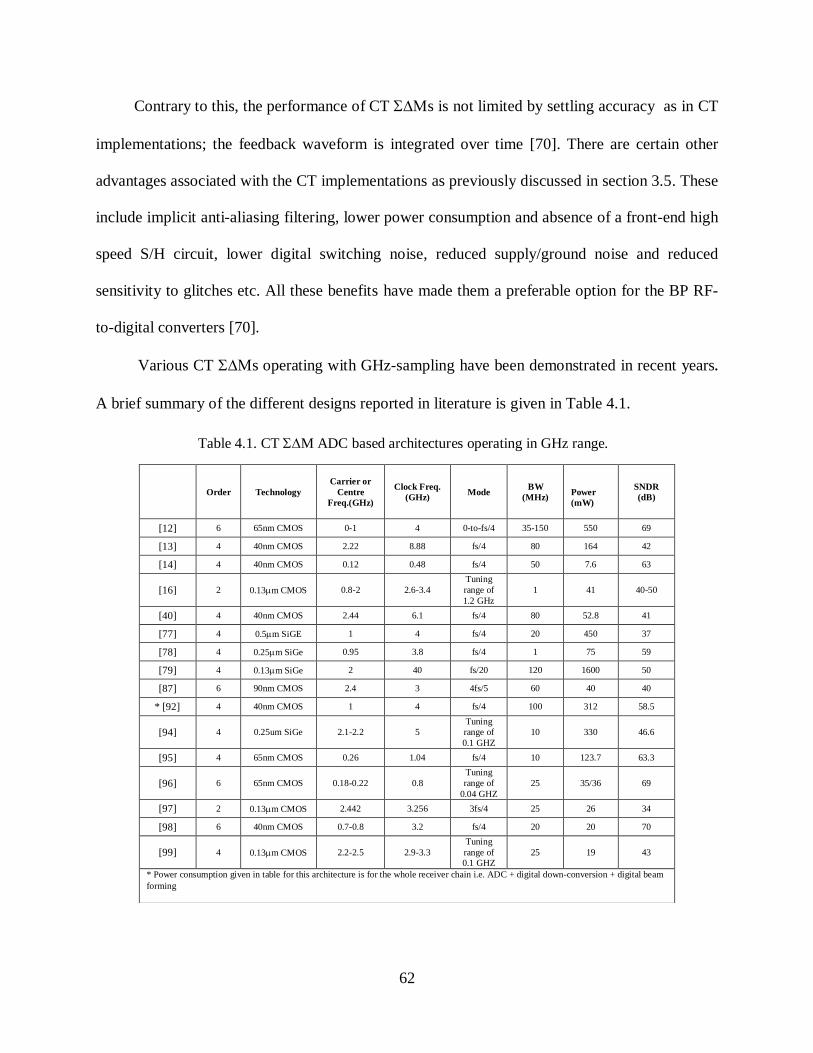
62
Contrary to this, the performance of CT s is not limited by settling accuracy as in CT
implementations; the feedback waveform is integrated over time [70]. There are certain other
advantages associated with the CT implementations as previously discussed in section 3.5. These
include implicit anti-aliasing filtering, lower power consumption and absence of a front-end high
speed S/H circuit, lower digital switching noise, reduced supply/ground noise and reduced
sensitivity to glitches etc. All these benefits have made them a preferable option for the BP RF-
to-digital converters [70].
Various CT s operating with GHz-sampling have been demonstrated in recent years.
A brief summary of the different designs reported in literature is given in Table 4.1.
Order Technology
Carrier or
Centre
Freq.(GHz)
Clock Freq.
(GHz) Mode
BW
(MHz)
Power
(mW)
SNDR
(dB)
[12] 6 65nm CMOS 0-1 4 0-to-fs/4 35-150 550 69
[13] 4 40nm CMOS 2.22 8.88 fs/4 80 164 42
[14] 4 40nm CMOS 0.12 0.48 fs/4 50 7.6 63
[16] 2 0.13m CMOS 0.8-2 2.6-3.4
Tuning
range of
1.2 GHz
1 41 40-50
[40] 4 40nm CMOS 2.44 6.1 fs/4 80 52.8 41
[77] 4 0.5m SiGE 1 4 fs/4 20 450 37
[78] 4 0.25m SiGe 0.95 3.8 fs/4 1 75 59
[79] 4 0.13m SiGe 2 40 fs/20 120 1600 50
[87] 6 90nm CMOS 2.4 3 4fs/5 60 40 40
* [92] 4 40nm CMOS 1 4 fs/4 100 312 58.5
[94] 4 0.25um SiGe 2.1-2.2 5
Tuning
range of
0.1 GHZ
10 330 46.6
[95] 4 65nm CMOS 0.26 1.04 fs/4 10 123.7 63.3
[96] 6 65nm CMOS 0.18-0.22 0.8
Tuning
range of
0.04 GHZ
25 35/36 69
[97] 2 0.13m CMOS 2.442 3.256 3fs/4 25 26 34
[98] 6 40nm CMOS 0.7-0.8 3.2 fs/4 20 20 70
[99] 4 0.13m CMOS 2.2-2.5 2.9-3.3
Tuning
range of
0.1 GHZ
25 19 43
* Power consumption given in table for this architecture is for the whole receiver chain i.e. ADC + digital down-conversion + digital beam
forming
Table 4.1. CT M ADC based architectures operating in GHz range.

63
An important example is [13], which can digitize the signals located at 2.22 GHz while
operating at an fS of 8.88 GHz. One notable implementation is reported in [87], that employs
sub-sampling technique to enable the ADC to digitize the signals located at 2.4 GHz with fS of 3
GHz. Architecture reported in [94] is another interesting implementation. It is a tuneable 4th
-order
CT designed in 0.25-m SiGe BiCMOS technology that employs an fS of 3 GHz, while the
fN can be tuned over the range of 2.1-to-2.2 GHz. Two other examples are [95] and [96] which
are 4th
and 6th
order modulators, respectively. These ADCs operate at fS of 1.04 and 0.8 GHz
while digitizing the signals located at 0.26 and 0.18-to-0.22 GHz, respectively. [97] and [98] are
two other important examples operating at fS of 3.256 and 3.2 GHz, respectively while digitizing
the signals located at 2.442 and 0.7-to-0.8 GHz. Both of these ADCs employ LC BP filters. The
most recent example is [99] that also employ LC BP filters. While employing a sampling rate of
2.9-to-3.3 GHz, this ADC can digitize the signals located over the range of 2.4-to-2.5 GHz.
Most of the state-of-art BP-ΣΔMs (as described in Table 4.1) operate in the GHz range and
employ a fixed centre (or notch or fN). The applied input RF signals need to be placed within the
passband of the modulator for the proper digitization. Considering the SDR receiver architecture
from Figure 4.3, in order to digitize the complete RF spectrum, a tuneable phase locked loop
(PLL) synthesiser would be required to operate over a larger range of frequencies. Moreover,
variable output data rates complicate the interface of the modulator and DSP.
Another solution to this issue is to use the reconfigurable BP CT-ΣΔMs with tuneable fN
that can reduce the need of widely tuneable PLL. However, very few BP CT-ΣΔMs with
tuneable fN have been proposed until now. One such implementation is reported in [12]. It is a
sixth order modulator that operates at 2-to-4 GHz with the tuning range of DC-to-1 GHz.
Another important example [16] proposed an architecture with a tuneable range of 0.8-to-2 GHz.

64
One of the critical considerations of such CT BP-ΣΔMs is the implementation of the loop
filters. Most of the reported modulators (targeting SDR applications) have been implemented
with LC resonators. These resonators show better performance in terms of power, linearity and
speed compared to Gm-RC or Gm-C resonators at higher frequencies [100]. However, the major
limitation of LC resonator-based modulators is that only one feedback loop is supplied to a
simple LC filter. It does not give the proper loop impulse response to realise the required notch
NTF with full control over tuning of feedback coefficients which are required for a tuneable fN
[77]. The LC resonator has a second-order TF while it has only one internal node in the
modulator. As a result, CT-to-DT equivalence becomes impossible due to the loss of parity
between the order of the loop filter and the number of internal nodes. One approach to overcome
this problem has been reported in [77]. It is an LC BP-ΣΔM that employs two types of feedback
waveforms (RZ DAC and HRZ DAC), which provides enough degrees of freedom for the CT-to-
DT equivalence [77]. Another important technique (known as FIR technique) employs multiple
paths with non-return-to-zero (NRZ) DAC and different fractional clock delays [101] [102].
This above analysis indicates that BP ADCs required in the SDR receiver architecture of
Figure 4.3 can be realised with CT BP-ΣΔMs. These BP-ΣΔMs need to have a wide tuning of fN
and can be implemented with LC resonators due to their better performance at higher sampling
rates. In the following sections, firstly the specifications of such BP-ΣΔM ADC are derived.
Following that a design methodology for the synthesis of widely tuneable LC resonator-based
BP CT-ΣΔMs architecture is presented.
4.4 Modulator Specifications
The conceptual block diagram of the SDR receiver, shown in Figure 4.3, has been used
for the derivation of specifications for the targeted CT BP-. In this architecture, the input

65
signal, after being filtered and pre-amplified by the LNA, is digitized by a CT BP- and the
subsequent signal processing is carried out by a DSP in digital domain. The focus of this section
is to derive a meaningful set of specifications for the ADC to ensure that the input signal can be
appropriately digitized.
For the successful digitization of a signal, it should be able to work properly over the
whole DR of input while satisfying the minimum NF and linearity requirements. The required
SNR for the ADC depends on two important factors namely, the noise floor and the signal
power. The fundamental noise floor is due to the atmospheric noise received by the antenna and
is given by [41]:
dBs 1740.001
B.T10logPSD
.
(4.1)
Where B is the Boltzmann‟s constant (1.38x10⁻²³
J/K) and T is the temperature in Kelvin. For the
incoming signal having a bandwidth of BW, the rms noise power can be written as [41]:
BW10log10dBs174PSD_noise
(4.2)
The LNA and the filter (as shown in Figure 4.3), also introduce some noise in the signal path. If
the total noise figure from the antenna to the ADC input is NF (dB), then the total noise at the
ADC input is increased by NF (dB). Hence, the required SNR of ADC can be written as:
GAINnoiseC LNANFBW10logPSDPSNR .
(4.3)
Where PC is the maximum input power (i.e. blocker) after attenuation due to the off-chip filters,
BW is the bandwidth of desired band that needs to be converted, NF is the noise figure up to
input of ADC (including LNA and filter) and LNAGAIN is the gain of the LNA.

66
In order to derive the required specifications of the M ADC, different wireless
standards considered are GSM, EDGE, GPRS, CMDA-2000, WCDMA, WLAN (IEEE
802.11a/b/n), WiMAX and LTE. For the whole range of wireless standards, the ADC
specification derivation is quite complicated and involves multiple trade-offs between LNAGAIN,
input signal level, maximum blocker level, NF etc. The LNAGAIN for most of the wireless
receivers is between 15-to-20 dBs [103]-[105]. Furthermore, in modern wireless receivers due to
the lower quality factor (Q) of the on-chip BP filters, out-of-band blockers are typically
attenuated by off-chip SAW filters prior to LNA [104]. Therefore, by employing the expression
of required SNR of ADC from equation (4.3), while considering an LNAGAIN of 15dB, on/off
chip of 15 dB blocker attenuation, a NF of 3 dB and taking a number published works ([5][12]-
[19][28][39][40][64][65][67][71][77]-[80][106][107]) into account, Table 4.2 has been derived.
This table serves as a reference for the achievable performance of the proposed architecture.
Table 4.2. Resolution requirements for different wireless communication standards.
Standard Carrier Frequency (MHz) Bandwidth (MHz) SNR (dBs)
GSM 850-1900 0.2 90
EDGE 850-1900 0.2 90
GPRS 850-1900 0.2 90
CDMA 450-2100 1.25 65
IEEE 802.11a 5000 20 50
IEEE 802.11b 2400 5.5 50
IEEE 802.11n 2400/5000 20/40 50
LTE 700-3500 5/10/20/40/100 70-75

67
4.5 Sub-sampling
In order to handle all the standards mentioned in Table 4.2 , the ADC is required to digitize
the signals with carrier frequencies ranging from 0.455 GHz (CDMA-2000) to 5.093 GHz
(WiMAX) with channel bandwidths varying from 0.2 MHz (GSM) to 30 MHz (LTE).
The sampling rates in conventional BP-Ms are typically four times of the input frequency
(or fN), which simplifies the subsequent down conversion in the digital domain [50]. When such
ADCs are used for input signals located in the GHz range, the sampling rates become
prohibitively high. As an example, considering the WiMAX standard with a signal band located at
5.093 GHz would require a sampling rate of 20.372 GHz. Such higher sampling rates pose several
design related issues. First, the specifications of the different building blocks of the ADC increase
directly with the sampling rates [28][77]. Moreover, the performance of the CT BP-M ADCs is
very sensitive to the clock jitter in the feedback path [70]. Realising the clock generation circuit
with such higher sampling rates with lower jitter is difficult and challenging [108]. The power of
the DSP following the ADC is also directly proportional to the operating frequency.
Sub-sampling is an efficient way to overcome the challenge of operating at higher
sampling rates. In these architectures, the input signal located at a certain high frequency is
sampled with the sampling rates lower than the Nyquist-rate [109]. The bandwidth of the signal
of interest is usually much lower than the sampling rates. The resultant signal bandwidth is still
oversampled thereby avoiding aliasing between replicas. An ideal S/H block operating at a
sampling frequency of fS generates aliases of input and image signal. Assume the input of the S/H
block is an RF signal located at a frequency, fRF, such that fRF is much higher than fS. At the
output of the S/H, aliases of the input signal are located at mfS + fRF where “m” is an integer

68
number, as depicted in Figure 4.4. Furthermore, aliases of the image signal exist at (m + 1) fS –
fRF. The alias of the original signal or the image signal located within the range 0-to- fS/2 can be
used to extract the original RF signal [87] [97].
The same concept can be extended to the BP- ADCs. If an RF signal is passed
through a sub-sampled M, one alias of the signal exists at a lower frequency fN, within range
0-to- fs/2 and that can be calculated as [110]
odd0.5f
fif),f,(fremf
even0.5f
fif),f,(frem
f
S
RFSRFS
S
RFSRF
N
(4.4)
fs mfs
(m+½)fsfs/2 3fs/2-fs/2-3fs/2-(m+½)fs
-fs-mfs
f
f
(a)
(b)
fRF-fRF
Figure 4.4. (a) Input signal at frequency fRF to an ideal S/H operating at fS (b) Output of the S/H
showing the replicas of the original and image signal.
69
Where, rem(x, y) stands for the remainder of x and y. Equation (4.4) can be employed to
realise a sub-sampled BP- ADC. For a given standard, if fS and fRF are selected in a way
that fN is equal to the centre frequency of BP-M, one replica of the input (RF) signal can be
extracted with the noise shaped at fN. As an example, assume a BP- ADC is operating at a
sampling frequency of fS, with a passband centre frequency of fS/5. Assume an incoming signal
located at frequency of 4/5fS, is input to theADC. Therefore, using equation (4.4):
odd10.5f
f
S
RF
.
Therefore: /5f )f,(fremf f SSRFSN .
Hence, as depicted in Figure 4.5, the output spectrum of the M ADC has one digitized
alias of the input signal with quantisation noise shaped at fS/5. This alias is considered as the
output signal of interest and can be applied to the DSP for the further signal processing (such as
downconversion, filtering, channel selection etc.).
Output signal (Replica of
input signal)
fs/2 fs
f
(a)
4fs/5 fs/2 fs
f
(b)
4fs/5fs/5
Input SignalInput signal
Magnitude
(dB)Quantisation NoiseMagnitude
(dB)
Figure 4.5. (a) Input of BP- ADC with a centre frequency of 4/5 fS (b) Output
spectrum of BP- ADC with quantisation noise shaping at fS/5 [111].

70
For a sub-sampled M ADC, to down-convert an RF signal without overlapping, three
conditions need to be fulfilled:
· fS > 2BW (Nyquist theorem),
· fN – BW/2 > 0,
· fN < fS – BW/2.
As an example, consider the GSM/EDGE_850 standard that has a carrier frequency of 881.5
MHz and the BW of the signal of interest is 25 MHz. Using (4.4), a sub-sampled M ADC
centred at 118.5 MHz, operating at fS of 1 GHz sampling rate, can be used to digitize the input
signal.
4.5.1 Raised Cosine DAC
Two important limitations associated with the sub-sampled BP- ADC are
attenuation of the feedback signal (i.e. output of feedback DAC in M loop) and jitter in the
feedback DAC waveform.
In the M loop, input signal is largely attenuated by feedback DAC. Figure 4.6 shows
the frequency response of the different rectangular shaped DACs ([16][116]). The DACs i.e.
NRZ, RZ and HRZ behave as LP filters. Therefore, the signal located at fRF being fed back is
attenuated and as a result of that the SNR of the modulator is degraded. In order to overcome this
issue, the bandwidth of the feedback DAC needs to be increased. One approach to alleviate this
issue was proposed in [112] and [113]. With the zero insertion at the output of the quantiser, the
bandwidth of the feedback signal is increased and hence feedback signal degradation can be
reduced. Employing sine-shaped DACs, e.g. raised-cosine DAC, strength of feedback signals can
also be increased [114] [115]. Figure 4.7 illustrates the time domain plot of a raised-cosine DAC.

71
The frequency response of different shaped DACs (shown in Figure 4.6) depicts that raised-
cosine DACs have better magnitude response at frequencies larger than fS compared to NRZ and
RZ DACs. Another important advantage of the raised-cosine DAC is associated with the timing
jitter as shown in Figure 4.8 (a) and (b) [16]. Rectangular shaped DACs i.e. (NRZ, RZ and HRZ)
are more sensitive to feedback pulse jitter at the rising and falling edges of the feedback as the
slope of the pulse is maximum at those instants [70]. M
ag
nit
ud
e (
dB
)
Normalized Frequency ( fS )
1 2 3 4
NRZRaised Cosine
RZ
Figure 4.6. Frequency response of NRZ, RZ and raised-cosine DACs.
1/fS0Time
Amplitude
Figure 4.7. Graphical illustration of a sine-shaped DAC (Raised cosine DAC).
1/fS0 1/fS0 1/fS0
NRZ DAC
RZ DAC Raised cosine DACAmplitude
(a)
Amplitude Amplitude
(b) (c)
Time Time Time
Figure 4.8. Illustration of timing jitter on 3 types of DACs (a) NRZ DAC (b) RZ DAC and (c) Raised cosine DAC.

72
In the raised-cosine DACs, the sinusoidal pulse and the sampling clock are aligned
therefore, the DAC gets switched during sampling instant of the sinusoidal pulse. Hence, the
slope of the feedback pulse is zero at this instant, making it less sensitive to the timing jitter as
depicted in Figure 4.8 (c). Another important advantage associated with these DACs is the
removal of inter-symbol interference (ISI) [16][70]. Due to these reasons raised-cosine DACs are
a preferred option in higher sampling rates sub-sampled CT BP- ADCs [16] [97][117].
4.5.2 Sampling Frequency Selection
In order to determine the fS for a sub-sampled BP-M ADC in a SDR receiver, as shown
in Figure 4.3, a number of wireless standards (GSM, EDGE, GPRS, CMDA-2000, WCDMA,
Bluetooth, WLAN (IEEE 802.11a/b/n), WiMAX and LTE) have been considered. Handling of
all these operating modes in the ADC requires that the signals are digitized with carrier
frequencies ranging from 0.455 to 5.093 GHz and with channel bandwidths varying from 0.2-to-
30 MHz. As mentioned in section 4.3, the sampling rates in conventional BP-Ms are typically
four times the input (or notch) frequency. Therefore, for higher input frequencies, sub-sampling
can be employed. Using the relation given in equation (4.4) and taking the three basic conditions
of sub-sampling ( fS > 2BW (Nyquist theorem), fN – BW/2 > 0 and fN < fS – BW/2 ) into
account, fS and fN for the different wireless communication standards have been calculated and
are summarised in Table 4.3. As a summary of this table, a CT BP-M with fN range of 0.04-
to-0.2485fS, capable of operating at fS of 1-to-2 GHz, can ideally digitize the wider range of
wireless standards.
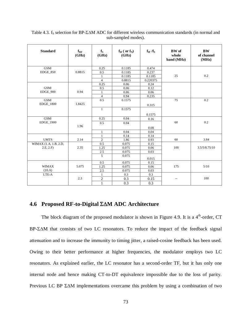
73
Table 4.3. fS selection for BP-M ADC for different wireless communication standards (in normal and sub-sampled modes).
Standard
fRF
(GHz)
fS
(GHz)
fIF ( or fN)
(GHz)
fIF /fS
BW of
whole
band (MHz)
BW
of channel
(MHz)
GSM/
EDGE_850
0.8815
0.25 0.1185 0.474
25
0.2 0.5 0.1185 0.237
1 0.1185 0.1185
4 0.8815 0.220375
GSM/
EDGE_900
0.94
0.25 0.06 0.24
0.5 0.06 0.12
1 0.06 0.06
4 0.94 0.235
GSM/
EDGE_1800
1.8425
0.5 0.1575
0.315
75 0.2
1 0.1575
0.1575
GSM/
EDGE_1900
1.96
0.25 0.04 0.16
60
0.2 0.5 0.04
0.08
1 0.04 0.04
UMTS
2.14
1 0.14 0.14
60
3.84 2 1.86 0.93
WIMAX (1.A, 1.B, 2.D,
2.E, 2.F)
2.35
0.5 0.075 0.15
100
3.5/5/8.75/10 1.25 0.075 0.06
2.5 0.075 0.03
5 0.075 0.015
WIMAX
(10.A)
5.075
0.5 0.075 0.15
175
5/10 1.25 0.075 0.06
2.5 0.075 0.03
LTE-A
2.3
1 0.3 0.3
--
100 2 0.3 0.15
1 0.3 0.3
4.6 Proposed RF-to-Digital M ADC Architecture
The block diagram of the proposed modulator is shown in Figure 4.9. It is a 4th-order, CT
BP-M that consists of two LC resonators. To reduce the impact of the feedback signal
attenuation and to increase the immunity to timing jitter, a raised-cosine feedback has been used.
Owing to their better performance at higher frequencies, the modulator employs two LC
resonators. As explained earlier, the LC resonator has a second-order TF, but it has only one
internal node and hence making CT-to-DT equivalence impossible due to the loss of parity.
Previous LC BP ΣΔM implementations overcame this problem by using a combination of two
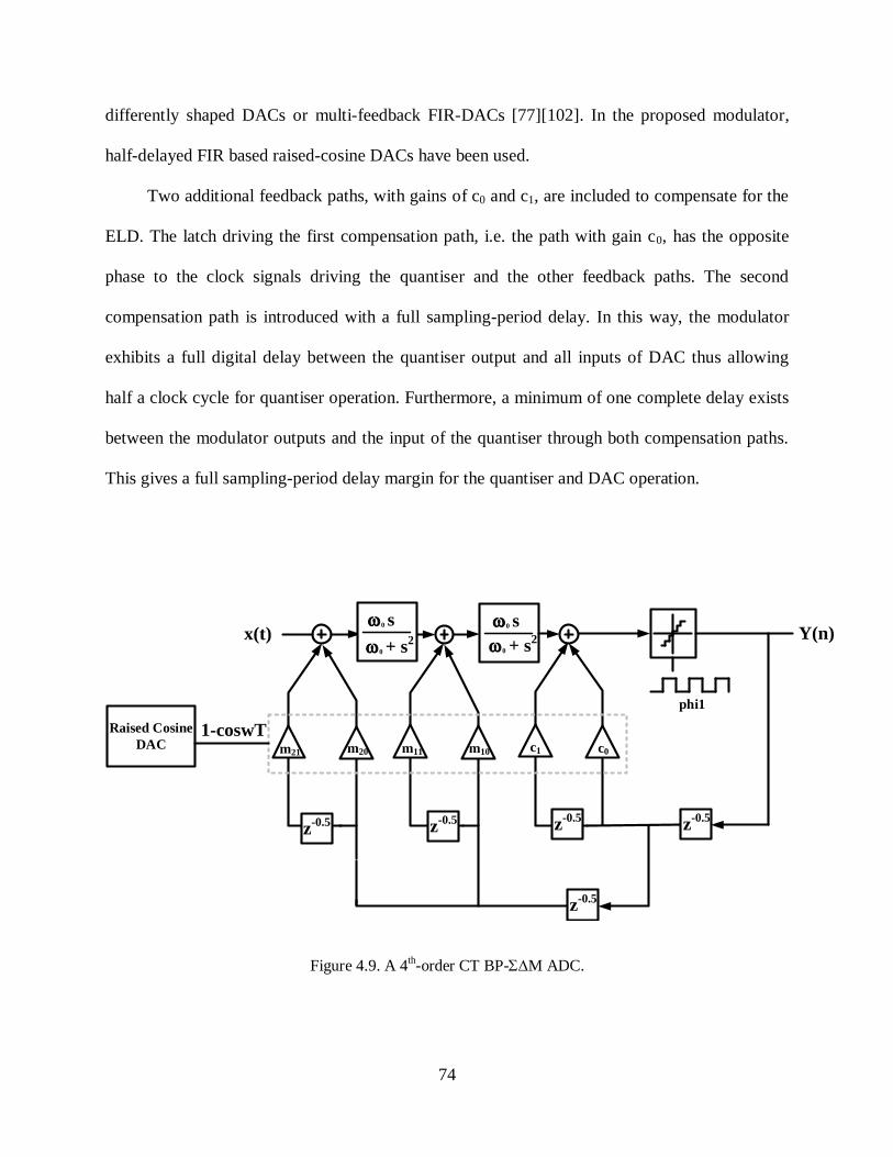
74
differently shaped DACs or multi-feedback FIR-DACs [77][102]. In the proposed modulator,
half-delayed FIR based raised-cosine DACs have been used.
Two additional feedback paths, with gains of c0 and c1, are included to compensate for the
ELD. The latch driving the first compensation path, i.e. the path with gain c0, has the opposite
phase to the clock signals driving the quantiser and the other feedback paths. The second
compensation path is introduced with a full sampling-period delay. In this way, the modulator
exhibits a full digital delay between the quantiser output and all inputs of DAC thus allowing
half a clock cycle for quantiser operation. Furthermore, a minimum of one complete delay exists
between the modulator outputs and the input of the quantiser through both compensation paths.
This gives a full sampling-period delay margin for the quantiser and DAC operation.
Raised Cosine
DAC c0
1-coswT
phi1
x(t) Y(n)
c1m21 m20 m11 m10
w0 s
w0 + s2
w0 s
w0 + s2
z-0.5
z-0.5 z
-0.5z
-0.5z
-0.5
Figure 4.9. A 4th-order CT BP-M ADC.
75
Compared to previous approaches based on raised-cosine FIR feedback DACs [102] , this
architecture uses a two-tap FIR structure instead of a three-tap. Therefore, the total number of
feedback paths required is 6 (which is much smaller than 16 reported in [102]). This reduction in
the number of the loop-filter coefficients improves the coefficient mismatch performance. The
mismatches are particularly critical in SDR applications, since a high degree of configurability in
coefficients is required to support widely programmable notches.
4.7 Design Methodology for CT BP-M with Reconfigurable fN (0-to-0.25
fS)
Three steps of the proposed design methodology steps for the system level design of the CT
BP-M ADC consisting of 2 LC resonators, targeting the RF-digitization are given in the
follows:
1. The calculation of the feedback and the feedforward coefficients of the 4th
-order CT BP-
M ADC, which consists of two LC resonators, depicted in Figure 4.9, for range of notch
frequencies (ranging from 0-to-0.25 fS) [88].
2. By using the sub-sampling technique, signals located at frequencies higher than 0.5fS can be
translated to the lower notch frequencies and subsequently converted. If fS is selected in such
a way that RF signals lie within the range 0.75fS -to-fS , 1.75fS-to-2fS, 2.75fS-to-3fS, 3.75fS-
to-4fS , 4.75fS-to-5fS, etc. then a replica of these signals is translated to frequency range of 0-
to-0.25fS. Other replicas are located at 1-to-1.25fS, 2-to-2.25fS and so on.
3. Using the coefficients derived in step 1, RF signals located at much higher frequencies can be
successfully digitized.

76
The design flow adopted for the modulator with a reconfigurable fN (ranging from 0-to-0.25fS) is
as follows:
Step 1: The NTF of a 4th-order BP DT-M for the different notches is calculated.
Step 2: Using a modified-Z transform technique, the coefficients of the continuous time LC
BP-M (equivalent to first step DT BP-M ADC) are calculated.
Step 3: Using these coefficients, an ideal system level model is simulated and then the output
is processed, in Matlab® [119].
Three steps of the above-mentioned methodology are elaborated for the case of an fN =
0.2fS in the following. The same methodology can also be used for the derivation of the
coefficients for other notches as well.
1. NTF for a 4th
-order BP-DTM
By replacing a LP filter in the M ADC with a BP filter, noise suppression can be
obtained at the resonance frequency of the filter. A discrete time low-pass TF can be transformed
into a band-pass TF with lower and upper cut-off frequencies, wc1 and wc2, respectively using
following expression [66]:
1z1k
2kαz
1k
1k1k
1kz
1k
2kαz-
z1-2-
1-2-
1-
. (4.5)
where “"and “k” are passband scaling parameters and given respectively by:
2
ωωcos
2
ωωcos
αC1C2
C1C2
, (4.6)
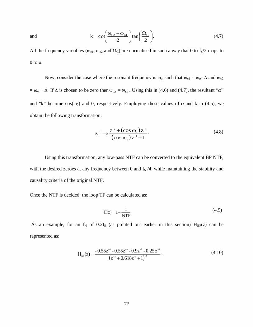
77
and
2
Ω tan
2
ωωcotk CC1C2 . (4.7)
All the frequency variables (wc1, wc2 and ΩC) are normalised in such a way that 0 to fS/2 maps to
0 to π.
Now, consider the case where the resonant frequency is w such that wc1 = w- and wc2
= w + If is chosen to be zero then C1C2 ωω . Using this in (4.6) and (4.7), the resultant “”
and “k” become cos(w) and 0, respectively. Employing these values of and k in (4.5), we
obtain the following transformation:
1z ω cos
z ω cosz z
1
0
1
0
2
1
. (4.8)
Using this transformation, any low-pass NTF can be converted to the equivalent BP NTF,
with the desired zeroes at any frequency between 0 and fS /4, while maintaining the stability and
causality criteria of the original NTF.
Once the NTF is decided, the loop TF can be calculated as:
NTF
1 1H(z) (4.9)
As an example, for an fN of 0.2fS (as pointed out earlier in this section) HBP(z) can be
represented as:
212
1234
BP
10.618zz
z 0.25-0.9z-0.55z-0.55z- (z)H
. (4.10)

78
2. Modified-Z Transform Technique for CT-DT Transformation
In order to realise a DT NTF using a 4th
-order LC resonator based CT BP-M, as shown
in Figure 4.9, a CT-to-DT transformation is required. These two modulators are equivalent if, for
a given input waveform, the input to the quantiser at the sampling instants are equal as depicted
in Figure 4.10 (a) and (b) [70]. It can be represented as [16]:
SnTt
11 H(z)Z(G(s))L
. (4.11)
x(t) Y(n)
DAC
HBP(z)q(n)
y(t)
HBP(z)DACY(n) u(n)
(a)
x(t) Y(n)
DAC
HBP(s)q(n)
y(t)
HBP(s)Y(n)
HDAC(s)
HDAC(s)
fS
q(n)
fS
G(s)
(b)
Figure 4.10. Loop filter in M for (a) DT implementation (b) CT implementation.
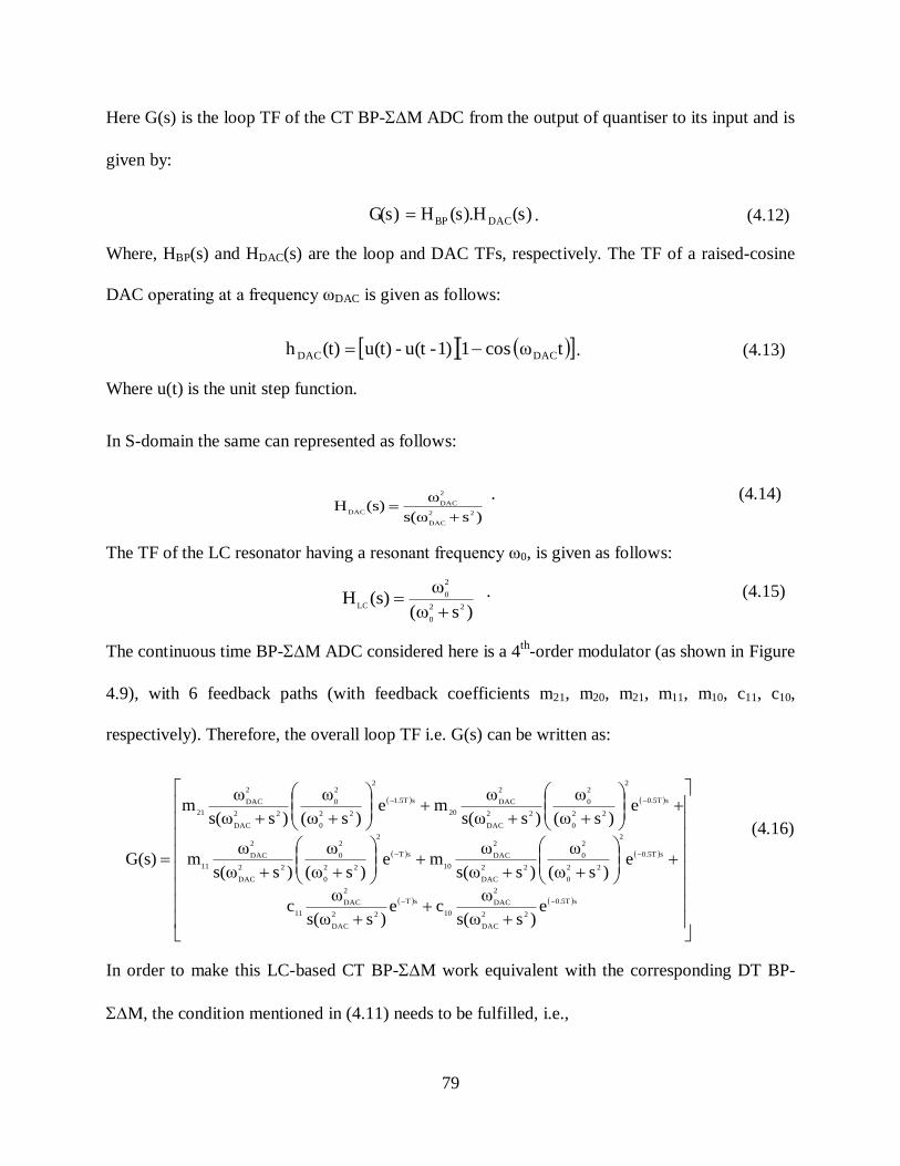
79
Here G(s) is the loop TF of the CT BP-M ADC from the output of quantiser to its input and is
given by:
(s)(s).HHG(s) DACBP . (4.12)
Where, HBP(s) and HDAC(s) are the loop and DAC TFs, respectively. The TF of a raised-cosine
DAC operating at a frequency ωDAC is given as follows:
tω cos11)-u(t - u(t)(t)h DACDAC . (4.13)
Where u(t) is the unit step function.
In S-domain the same can represented as follows:
)ss(ω
ω(s)H
22
DAC
2
DAC
DAC
. (4.14)
The TF of the LC resonator having a resonant frequency ω0, is given as follows:
)sω(
ω(s)H
22
0
2
0
LC
. (4.15)
The continuous time BP-M ADC considered here is a 4th
-order modulator (as shown in Figure
4.9), with 6 feedback paths (with feedback coefficients m21, m20, m21, m11, m10, c11, c10,
respectively). Therefore, the overall loop TF i.e. G(s) can be written as:
s0.5T
22
DAC
2
DAC
10
sT
22
DAC
2
DAC
11
s0.5T
2
22
0
2
0
22
DAC
2
DAC
10
sT
2
22
0
2
0
22
DAC
2
DAC
11
s0.5T
2
22
0
2
0
22
DAC
2
DAC
20
s1.5T
2
22
0
2
0
22
DAC
2
DAC
21
e)ss(ω
ωce
)ss(ω
ωc
e)sω(
ω
)ss(ω
ωme
)sω(
ω
)ss(ω
ωm
e)sω(
ω
)ss(ω
ωme
)sω(
ω
)ss(ω
ωm
G(s)
(4.16)
In order to make this LC-based CT BP-M work equivalent with the corresponding DT BP-
M, the condition mentioned in (4.11) needs to be fulfilled, i.e.,

80
H(z)(G(s))LZ 1 . (4.17)
For a 4th-order BP modulator with a notch frequency of 0.2fS (based upon the example
mentioned at the start of this section), we have the following relationship:
212
1234
BP
10.618zz
z 0.25-0.9z-0.55z-0.55z- (z)H
(4.18)
Therefore:
212
12341
10.618zz
z -0.250.9z-0.55z-0.55z- (G(s))LZ
(4.19)
For CT-to-DT transformation of this architecture, the modified Z-transform technique is
used. The FIR-based DACs used here have half delays. The modified Z-transform is a promising
technique to calculate the Z transform of a CT system with delays which are not integral
multiples of sampling time [102]. The modified Z-transform of a function A(s) can be
represented as:
A(s) of poles pi mTs
mTs
m
)ez(
e A(s)of Residue sAZ . (4.20)
Using the modified Z-transform, the Z-transforms of all feedback paths of CT BP-M (i.e. m21,
m20, m11, m10, c10, c11) are calculated and their sum is equated with the corresponding DT loop
TF. The Z-transform of all the feedback paths is represented in partial fraction form. As an
example, the transfer functions of paths with two and one resonator have the partial fraction form
of:
z
b
z
b
z)(
a
z)(
a
z)(
a
z)(
a TF 2
2
1
*
22
2
*
1
2
1
r2_Resonato
ππππ
(4.21)
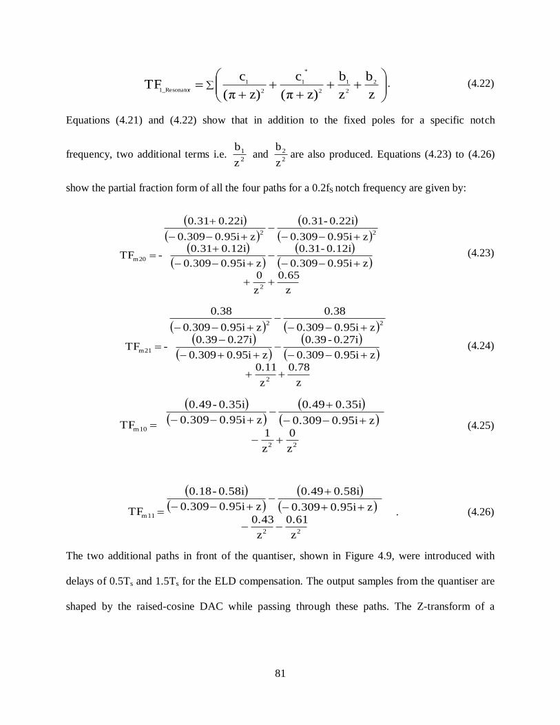
81
z
b
z
b
z)(
c
z)(
c TF 2
2
1
2
*
1
2
1
r1_Resonato
ππ. (4.22)
Equations (4.21) and (4.22) show that in addition to the fixed poles for a specific notch
frequency, two additional terms i.e. 2
1
z
b and
2
2
z
bare also produced. Equations (4.23) to (4.26)
show the partial fraction form of all the four paths for a 0.2fS notch frequency are given by:
z
0.65
z
0z0.95i0.309
0.12i-0.31
z0.95i0.309
0.12i0.31z0.95i0.309
0.22i-0.31
z0.95i0.309
0.22i0.31
- TF
2
22
m20
(4.23)
z
0.78
z
0.11z0.95i0.309
0.27i-0.39
z0.95i0.309
0.27i0.39z0.95i0.309
0.38
z0.95i0.309
0.38
- TF
2
22
m21
(4.24)
22
m10
z
0
z
1z0.95i0.309
0.35i0.49
z0.95i0.309
0.35i-0.49
TF
(4.25)
22
m11
z
0.61
z
0.43z0.95i0.309
0.58i0.49
z0.95i0.309
0.58i-0.18
TF
. (4.26)
The two additional paths in front of the quantiser, shown in Figure 4.9, were introduced with
delays of 0.5Ts and 1.5Ts for the ELD compensation. The output samples from the quantiser are
shaped by the raised-cosine DAC while passing through these paths. The Z-transform of a
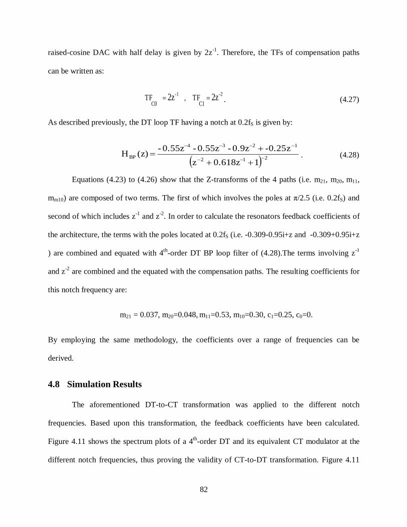
82
raised-cosine DAC with half delay is given by 2z-1
. Therefore, the TFs of compensation paths
can be written as:
-2-1 2z2zC1C0
TF , TF . (4.27)
As described previously, the DT loop TF having a notch at 0.2fS is given by:
212
1234
BP
10.618zz
z -0.250.9z-0.55z-0.55z- (z)H
. (4.28)
Equations (4.23) to (4.26) show that the Z-transforms of the 4 paths (i.e. m21, m20, m11,
mm10) are composed of two terms. The first of which involves the poles at π/2.5 (i.e. 0.2fS) and
second of which includes z-1
and z-2
. In order to calculate the resonators feedback coefficients of
the architecture, the terms with the poles located at 0.2fS (i.e. -0.309-0.95i+z and -0.309+0.95i+z
) are combined and equated with 4th
-order DT BP loop filter of (4.28).The terms involving z-1
and z-2
are combined and the equated with the compensation paths. The resulting coefficients for
this notch frequency are:
m21 = 0.037, m20=0.048, m11=0.53, m10=0.30, c1=0.25, c0=0.
By employing the same methodology, the coefficients over a range of frequencies can be
derived.
4.8 Simulation Results
The aforementioned DT-to-CT transformation was applied to the different notch
frequencies. Based upon this transformation, the feedback coefficients have been calculated.
Figure 4.11 shows the spectrum plots of a 4th-order DT and its equivalent CT modulator at the
different notch frequencies, thus proving the validity of CT-to-DT transformation. Figure 4.11

83
(a) to (c) illustrate the output spectrum plots at three notch frequencies, namely 0.12fS, 0.2fS, and
0.25fS, respectively. Figure 4.12 (a) to (c) depicts the output spectrum plots for the three different
cases while operating in normal and sub-sampling modes at the different values of input (fRF) and
sampling frequencies (fS). Figure 4.12 (a) shows the spectrum of an input frequency of 0.44
GHz with a sampling rate of 2 GHz. Figure 4.12 (b) and (c) illustrate the spectrum plots of two
sub-sampled cases for two input frequencies of 2.14 GHz and 5.2 GHz with sampling
frequencies of 1 and 2.5 GHz , respectively. Figure 4.13 depicts SNR-versus-input level curves
for these three cases proving the accuracy of the design methodology.
As stated in section 4.6, one of the benefits of the proposed architecture is the reduced
number of coefficients, which directly translates to lower mismatch sensitivity and circuit-
element tolerances. As an illustration of the robustness of the proposed modulator, Figure 4.14
shows the histogram of SNR of a 150-run Monte Carlo simulation. The variation in the
achievable SNR is for the three different cases namely 0.44 GHz with a sampling rate of 2 GHz
in normal mode, 2.14 GHz and 5.2 GHz in sub-sampling mode with sampling frequencies of 1
and 2.5 GHz, respectively). A standard deviation of 10% was considered in all the loop-filter
coefficients. The resultant maximum deviation of the SNR is within ±5 dBs. Table 4.4 shows the
achievable performance for the different input and sampling frequencies.

84
(a)
(b)

85
(c)
Figure 4.11. CT-to-DT transformation at three different notch frequencies (a) 0.12fS (b) 0.2fS (c)
0.25fS.
(a)

86
(b)
(c)
Figure 4.12. Modulator output spectra for the different cases of fRF and fS (a) fRF = 0.44 GHz, fS = 2 GHz (normal mode) (b) fRF = 2.14GHz, fS = 1 GHz (sub-sampling mode) and (c) fRF = 5.2 GHz, fS = 2.5 GHz
(sub-sampling mode).
0 0.1 0.2 0.3 0.4 0.5
-150
-100
-50
0Signal Spectrum
Mag
nitu
de (
dB
)
Frequency (GHz)
Output
0 0.2 0.4 0.6 0.8 1 1.2 1.4-200
-150
-100
-50
0Signal Spectrum
Mag
nitu
de (
dB
)
Frequency (GHz)
Output
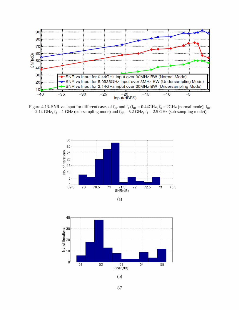
87
Figure 4.13. SNR vs. input for different cases of fRF and fS (fRF = 0.44GHz, fS = 2GHz (normal mode), fRF = 2.14 GHz, fS = 1 GHz (sub-sampling mode) and fRF = 5.2 GHz, fS = 2.5 GHz (sub-sampling mode)).
(a)
(b)
88
(c)
Figure 4.14. SNR histograms for the different cases of fRF and fS (a) fRF = 0.44GHz, fS = 2GHz (normal
mode) (b) fRF = 2.14GHz, fS = 1GHz (sub-sampling mode) and (c) fRF = 5.2 GHz, fS = 2.5 GHz (sub-sampling mode).
Table 4.4 . Summary of the achievable performance of the modulator in normal and sub-sampling
mode.
Mode fRF
(GHz)
fS
(GHz)
fN
(MHz)
f0
(fIF /fs )
BW
(MHz)
SNR
(dB)
Normal 0.15
-to-1
4 0.15
-to-1
0.0375
to
0.25
30 65
to
78
Sub-sampling 2.14 1 0.14 0.14 20 54
3.75 2 0.25 0.125 20 48
5.093 2.5 0.0938 0.0375 20 52
4.9 Conclusions
An outline of the different SDR based architectures was described in detail in this chapter. A
4th-order CT BP-M ADC with a raised-cosine FIR feedback DAC capable of operating in
normal and sub-sampling modes for RF-to-digital conversion was presented. The reduced
number of loop-filter coefficients in the design resulted in a better robustness to mismatch, while
ensuring the stability and complete equivalence between the discrete-time system and the
continuous-time implementation. The system level simulation results for three different wireless
communication standards spanning over an input frequency range of 0.44-to-5 GHz proved the
accuracy of the presented methodology and architecture. The same methodology can be extended

89
to other standards as well. These advantages make the presented modulator a suitable option for
direct RF digitization in next generation SDR mobile systems.

90
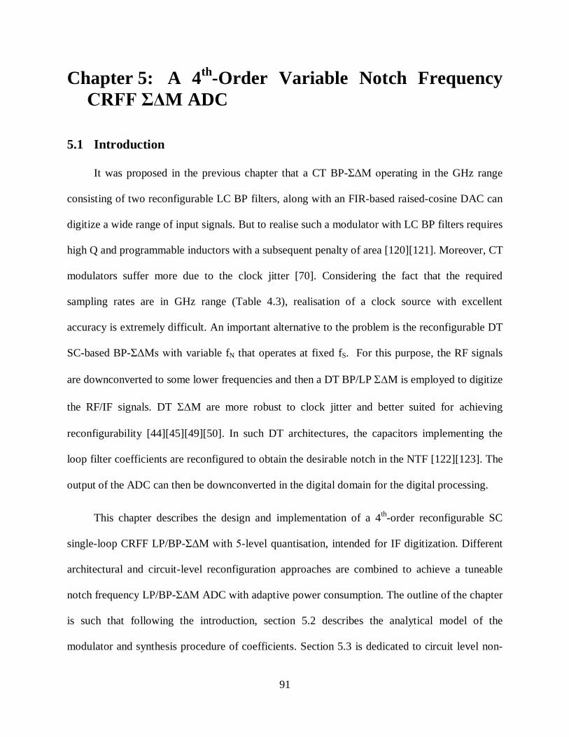
91
Chapter 5: A 4th
-Order Variable Notch Frequency
CRFF ΣΔM ADC
5.1 Introduction
It was proposed in the previous chapter that a CT BP-ΣΔM operating in the GHz range
consisting of two reconfigurable LC BP filters, along with an FIR-based raised-cosine DAC can
digitize a wide range of input signals. But to realise such a modulator with LC BP filters requires
high Q and programmable inductors with a subsequent penalty of area [120][121]. Moreover, CT
modulators suffer more due to the clock jitter [70]. Considering the fact that the required
sampling rates are in GHz range (Table 4.3), realisation of a clock source with excellent
accuracy is extremely difficult. An important alternative to the problem is the reconfigurable DT
SC-based BP-ΣΔMs with variable fN that operates at fixed fS. For this purpose, the RF signals
are downconverted to some lower frequencies and then a DT BP/LP M is employed to digitize
the RF/IF signals. DT M are more robust to clock jitter and better suited for achieving
reconfigurability [44][45][49][50]. In such DT architectures, the capacitors implementing the
loop filter coefficients are reconfigured to obtain the desirable notch in the NTF [122][123]. The
output of the ADC can then be downconverted in the digital domain for the digital processing.
This chapter describes the design and implementation of a 4th-order reconfigurable SC
single-loop CRFF LP/BP-ΣΔM with 5-level quantisation, intended for IF digitization. Different
architectural and circuit-level reconfiguration approaches are combined to achieve a tuneable
notch frequency LP/BP-ΣΔM ADC with adaptive power consumption. The outline of the chapter
is such that following the introduction, section 5.2 describes the analytical model of the
modulator and synthesis procedure of coefficients. Section 5.3 is dedicated to circuit level non-
92
idealities and the resulting behaviour of the modulator. The description of macromodel
implementation and corresponding results are given in section 5.4. The transistor-level
implementation of the whole modulator is described in section 5.5 while layout details are given
in section 5.6. Finally, section 5.7 details test-setup, experimental characterization and
comparison with other state of the art designs.
5.2 Modulator Architecture
A 4th
-order cascade of resonator with feedforward architecture has been selected for this
prototype because compared to its cascade of resonator with feedback (CRFB) counterpart, this
architecture requires a reduced number of coefficients. This essentially leads to less area
requirement in terms of capacitors and hence less silicon area and hence reduced cost [44].
A 4th
-order DT CRFF based M ADC consisting of two resonators is shown in Figure
5.1. Each resonator consists of one Forward-Euler (FE) and one Backward-Euler (BE) Integrator.
Two feedback coefficients (g1 and g2) across the integrators are used to realise resonators. A
direct feedforward path from the input to the adder guarantees a unity STF. This way, only the
error signal is processed by the internal integrators [124][125].
DAC
c1
b1
g1
c2 c3 c4
x(t)
b5
a4
a3
a2
a1
z-1
1-z-1
1
1-z-1
z-1
1-z-1
1
1-z-1
g2
Resonator 1 Resonator 2
Figure 5.1. Reconfigurable 4th-order CRFF M architecture.
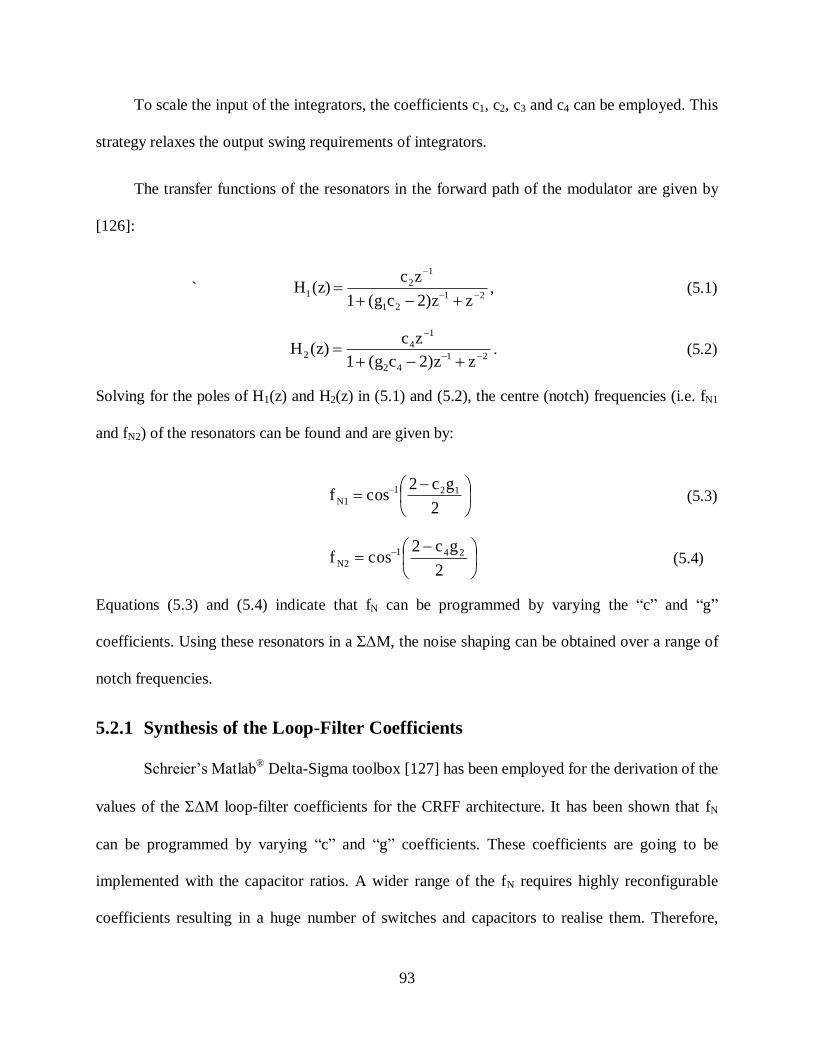
93
To scale the input of the integrators, the coefficients c1, c2, c3 and c4 can be employed. This
strategy relaxes the output swing requirements of integrators.
The transfer functions of the resonators in the forward path of the modulator are given by
[126]:
` 21
21
1
21
z2)zc(g1
zc(z)H
, (5.1)
21
42
1
42
z2)zc(g1
zc(z)H
. (5.2)
Solving for the poles of H1(z) and H2(z) in (5.1) and (5.2), the centre (notch) frequencies (i.e. fN1
and fN2) of the resonators can be found and are given by:
2
gc2cosf 121
N1 (5.3)
2
gc2cosf 241
N2 (5.4)
Equations (5.3) and (5.4) indicate that fN can be programmed by varying the “c” and “g”
coefficients. Using these resonators in a ΣΔM, the noise shaping can be obtained over a range of
notch frequencies.
5.2.1 Synthesis of the Loop-Filter Coefficients
Schreier‟s Matlab®
Delta-Sigma toolbox [127] has been employed for the derivation of the
values of the M loop-filter coefficients for the CRFF architecture. It has been shown that fN
can be programmed by varying “c” and “g” coefficients. These coefficients are going to be
implemented with the capacitor ratios. A wider range of the fN requires highly reconfigurable
coefficients resulting in a huge number of switches and capacitors to realise them. Therefore,
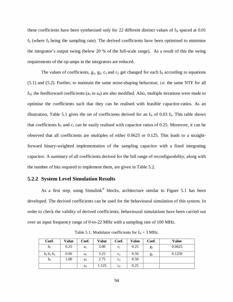
94
these coefficients have been synthesised only for 22 different distinct values of fN spaced at 0.01
fS (where fS being the sampling rate). The derived coefficients have been optimised to minimise
the integrator‟s output swing (below 20 % of the full-scale range). As a result of this the swing
requirements of the op-amps in the integrators are reduced.
The values of coefficients, g1, g2, c1 and c2 get changed for each fN according to equations
(5.1) and (5.2). Further, to maintain the same noise-shaping behaviour, i.e. the same NTF for all
fN; the feedforward coefficients (a1 to a4) are also modified. Also, multiple iterations were made to
optimise the coefficients such that they can be realised with feasible capacitor-ratios. As an
illustration, Table 5.1 gives the set of coefficients derived for an fN of 0.03 fS. This table shows
that coefficients b1 and c1 can be easily realised with capacitor ratios of 0.25. Moreover, it can be
observed that all coefficients are multiples of either 0.0625 or 0.125. This leads to a straight-
forward binary-weighted implementation of the sampling capacitor with a fixed integrating
capacitor. A summary of all coefficients derived for the full range of reconfigurability, along with
the number of bits required to implement them, are given in Table 5.2.
5.2.2 System Level Simulation Results
As a first step, using Simulink® blocks, architecture similar to Figure 5.1 has been
developed. The derived coefficients can be used for the behavioural simulation of this system. In
order to check the validity of derived coefficients, behavioural simulations have been carried out
over an input frequency range of 0-to-22 MHz with a sampling rate of 100 MHz.
Table 5.1. Modulator coefficients for fN = 3 MHz.
Coef. Value Coef. Value Coef. Value Coef. Value
b1 0.25 a1 3.00 c1 0.25 g1 0.0625
b2 b3 b4 0.00 a2 3.25 c2 0.50 g2 0.1250
b5 1.00 a3 2.75 c3 0.50
a4 1.125 c4 0.25

95
Table 5.2. Maximum and minimum values of all coefficients along with the number of bits required for
the implementation.
The results obtained in this way are processed in Matlab®. Figure 5.2 to Figure 5.9
represent the plots of input of a -6 dBFS input signal, at the different notches frequencies of 3, 6,
9, 12, 15, 18 and 22 MHz, respectively.
The same coefficients derived for fS =100 MHz can be used for fS = 200 MHz to increase
the tuning range of the notch to 44 MHz. As an illustration, Figure 5.10 shows the SNDR-versus-
amplitude curves obtained over the whole fN tuning range (0-to-44 MHz) and considering a signal
bandwidth of 1 MHz while employing sampling rates of 100 MHz and 200 MHz, respectively.
Figure 5.2. Output spectrum plot of an input of 300 kHz for ideal model with the ADC operating in the
LP-mode (fS =100 MHz).
0 10 20 30 40 50-250
-200
-150
-100
-50
0Signal Spectrum
Mag
nitu
de (
dB
)
Frequency (MHz)
Output
Coefficients Min. Max. No. Of Bits
b1 0.25 0.25 --
b2b3 b4 0 0 --
b5 1 1 --
a1 3 3 --
a2 0.125 3.875 5
a3 0.125 3.875 5
a4 0.125 3.875 5
c1 0.25 0.25 --
c2 0.125 1.875 4
c3 0.125 1.875 4
c4 0.125 1.875 4
g1 0.0625 1.875 5
g2 0.0625 1.875 5
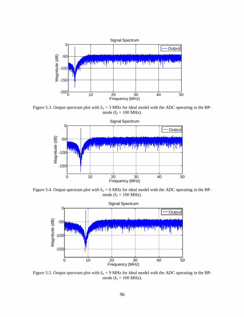
96
Figure 5.3. Output spectrum plot with fN = 3 MHz for ideal model with the ADC operating in the BP-mode (fS = 100 MHz).
Figure 5.4. Output spectrum plot with fN = 6 MHz for ideal model with the ADC operating in the BP-mode (fS = 100 MHz).
Figure 5.5. Output spectrum plot with fN = 9 MHz for ideal model with the ADC operating in the BP-
mode (fS = 100 MHz).
0 10 20 30 40 50-200
-150
-100
-50
0Signal Spectrum
Mag
nitu
de (
dB
)
Frequency (MHz)
Output
0 10 20 30 40 50
-150
-100
-50
0Signal Spectrum
Mag
nitu
de (
dB
)
Frequency (MHz)
Output
0 10 20 30 40 50
-150
-100
-50
0Signal Spectrum
Ma
gn
itud
e (
dB
)
Frequency (MHz)
Output
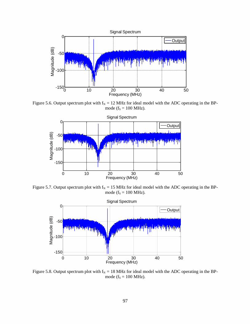
97
Figure 5.6. Output spectrum plot with fN = 12 MHz for ideal model with the ADC operating in the BP-mode (fS = 100 MHz).
Figure 5.7. Output spectrum plot with fN = 15 MHz for ideal model with the ADC operating in the BP-
mode (fS = 100 MHz).
Figure 5.8. Output spectrum plot with fN = 18 MHz for ideal model with the ADC operating in the BP-
mode (fS = 100 MHz).
0 10 20 30 40 50-150
-100
-50
0Signal Spectrum
Ma
gn
itu
de
(d
B)
Frequency (MHz)
Output
0 10 20 30 40 50
-150
-100
-50
0Signal Spectrum
Mag
nitu
de (
dB
)
Frequency (MHz)
Output
0 10 20 30 40 50
-150
-100
-50
0Signal Spectrum
Ma
gn
itu
de
(d
B)
Frequency (MHz)
Output

98
Figure 5.9. Output spectrum plot with fN = 22 MHz for ideal model with the ADC operating in the BP-
mode (fS = 100 MHz).
Figure 5.10. SNDR vs. input amplitude for a bandwidth of 1 MHz and fN from 0 to 44 MHz (while
employing fS = 100 MHz for the tuning range fN = 0-to-22 MHz and fS = 200 MHz over the tuning range fN
= 23-to-44 MHz).
5.3 Impact of Circuit Errors and High-Level Sizing
In order to transform the system-level architecture to a circuit-level implementation, a
systematic design flow has been adopted [128]. In this section, initially a capacitor calculation
strategy for a given in-band error (IBE), is examined. Following that, a parametric analysis of
different non-idealities of the op-amp employed in integrators and simulation results are
presented.
0 10 20 30 40 50-200
-150
-100
-50
0Signal Spectrum
Mag
nitu
de (
dB
)
Frequency (MHz)
Output
-60 -50 -40 -30 -20 -10 0 10
20
40
60
80
100
Input(dBFS)
SN
DR
(dB
)

99
5.3.1 Sampling Capacitor Calculations for a Given IBE
The major contribution of input referred noise for this ADC comes from the first
resonator [129][130]. In order to calculate the sampling capacitors, a conceptual single-ended SC
schematic shown in Figure 5.11 has been used. This schematic represents the arrangement of
integrators in the modulator. The four sampling capacitors in front of each of the four integrators
are represented by Csb1, Csc2, Csc3 and Csc4. While, Ci1 to Ci4 are the integrating capacitors of the
respective integrators. The sampling capacitors in front of adder‟s op-amp are Csb5, Csa2, Csa2,
Csa3 and Csa4. Moreover, Csg1 and Csg2 are two capacitors to implement resonance coefficients
(i.e. g1 and g2).
-
+
+-
P1 N1
Ø1d
Ø2
Vip
Vref-Vref+
Ø1
Csb1
Ci1
-
+
+Ø1
Ø1d
Csc2
Ci2
Ø2
Ø2d
-
-
+
+-
Ø1
Ø1d Csc3
Ci
3
Ø2
Ø2d
- +Ø1
Ø1d
Ci4
Ø2
Ø2d
-
+
+-
Ø1
Csa4
Cia
Ø2
Ø1d
Ø2d
Ø
1
Csa3
Ø
2
Ø1d
Ø2d
Ø1
Csa2
Ø2
Ø1d
Ø2d
Ø1
Csa1
Ø2Ø2d
Ø
1
Csb5
Ø2Ø2d
Ø1d
Ø1d
Ø1
Ø2
Csg1Ø2d
Ø1d
Ø1
Ø1d
Csg2
Ø2
Ø2d
Ø1
d1 .d5
Csc4
+-
Figure 5.11. Conceptual SC schematic of the loop filters and adder in the proposed M.
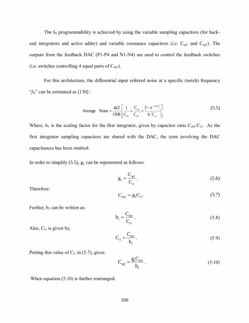
100
The fN programmability is achieved by using the variable sampling capacitors (for back-
end integrators and active adder) and variable resonance capacitors (i.e. Csg1 and Csg2). The
outputs from the feedback DAC (P1-P4 and N1-N4) are used to control the feedback switches
(i.e. switches controlling 4 equal parts of Csb1).
For this architecture, the differential input referred noise at a specific (notch) frequency
“fN” can be estimated as [130] :
2sc
2
1
2fN2i
2
sb1
sg1
sb1Cb
e1
C
C
C
1
OSR
4kTNoiseAverage
π
. (5.5)
Where, b1 is the scaling factor for the first integrator, given by capacitor ratio Csb1/Ci1. As the
first integrator sampling capacitors are shared with the DAC, the term involving the DAC
capacitances has been omitted.
In order to simplify (5.5), g1 can be represented as follows:
i1
sg1
1C
Cg . (5.6)
Therefore:
i11sg1 CgC . (5.7)
Further, b1 can be written as:
i1
sb11
C
Cb . (5.8)
Also, Ci1 is given by,
1
sb1i1
b
CC . (5.9)
Putting this value of Ci1 in (5.7), gives:
1
sb11sg1
b
CgC . (5.10)
When equation (5.10) is further rearranged:
101
2
sb1
sg1
C
C =
sb11
1
Cb
g. (5.11)
Putting value this value in (5.5), the average in-band noise can be written as:
2sc
2
1
2f)i2(
sb11
1
sb1 Cb
e1
Cb
g
C
1
OSR
4kTseAverageNoi .
(5.12)
Equation (5.12) shows various trade-offs of the sampling capacitor calculations. The
input referred noise is inversely related to the sampling capacitor in the first and second
integrators (i.e. Csb1 and Csc2) but increases with fN. As an illustration, Table 5.3 shows the
different values of Csb1 and Csc2 and the resultant IBE. Using this approach, different
combinations of Csb1 and Csc2 were investigated at different notch frequencies to have realisable
capacitance values, while maintaining the average IBE within a desirable range. The coefficient
b1 and hence the sampling capacitor of the first integrator (Csb1), remains the same over the
whole range of fN. In terms of second, third and 4th integrators, the sampling capacitors are
varied to realise the variable coefficients. Based on the required value of the sampling capacitor
for a specific fN, the switches can be turned ON or OFF to realise the desired value. A detailed
explanation about the SC implementation, along with detailed schematics of the capacitor
implementation will be explained in the next section.
Based on the above analysis, the values of all sampling, integrating and resonant
capacitors (used to implement g1 and g2) have been derived. Table 5.3 details the sampling
capacitor values of the front end two integrators and achievable IBE. The final values of the
modulator capacitors derived and number of bits required to implement them are given in Table
5.4. Finally, Table 5.5 summarises the binary weighted sampling and resonant capacitors for all
integrators.

102
Table 5.3. fN, sampling capacitors of first and second integrator and corresponding IBE.
No.
fN (MHz)
Average in-band noise (dB)
Csb1 (pF)
Csc2 (pF)
1 22 -89 0.25 1.237
2 13 -77 0.4 0.190
3 8 -87 0.5 0.175
4 2 -81 0.25 2.200
Table 5.4. Summary of the sampling and integrating capacitor values (pF).
Min. Max. Bits First Integrator Csb1 0.2 0.2 --
Csg1 0.05 1.55 5
Second Integrator Ci1 0.8 0.8 --
Csc2 0.1 1.5 4
Ci2 0.8 0.8 --
Third Integrator Csc3 0.1 1.5 4
Csg2 0.05 1.55 5
Ci3 0.8 0.8 --
Fourth
Integrator
Csc4 0.05 0.75 4
Ci4 0.4 0.4 --
Ca1 1.5 1.5 --
Ca2 0.05 1.55 5
Adder Ca3 0.05 1.55 5
Ca4 0.05 1.55 5
Cia 0.4 0.4 --
Table 5.5. Binary weighted sampling and resonant capacitors for 4 integrators
Integrator Capacitor Physical Value (pF)
First Integrator
Csb1 0.20
Cub1 0.05
Ci1 0.80
Second Integrator
Cuc1 0.10
Cuc2 0.20
Cuc3 0.40
Cuc4 0.80
Ci2 0.80
Third Integrator
Cuc1 0.05
Cuc2 0.10
Cuc3 0.20
Cuc4 0.40
Cuc5 0.80
Ci3 0.80
Fourth Integrator
Cuc1 0.05
Cuc2 0.10
Cuc3 0.20
Cuc4 0.40
Ci4 0.40
First Resonance Capacitor
Cug1 0.05
Cug2 0.10
Cug3 0.20
Cug4 0.40
Cug5 0.80
Second Resonance Capacitor
Cug1 0.05
Cug2 0.10
Cug3 0.20
Cug4 0.40
Cug5 0.80

103
5.4 Parametric Analysis of Op-amps Non-idealities
The non-idealities of the op-amps used to realise the integrators of the M ADC degrade
the TF of integrators and hence degrade the performance of the overall ADC. Most important of
these non-idealities include finite DC gain, limited transconductance, limited output currents and
input referred noise.
Considering an op-amp with a DC gain of Ao, The SC integrator‟s TF is given as
[28][131]:
1
O
s
1
O
ps
S
zA
g1
z
A
gg11gH(z)
. (5.13)
Where
i
s
S
C
Cg
,
and i
p
P
C
Cg
.
Here Cs, Ci and Cp are the sampling, integrating and input parasitic capacitances of the
integrator, respectively. Equation (5.13) shows that a finite DC gain results in a leaky integrator
and shifts the pole of the NTF. The finite DC gain becomes a major concern in the band-pass
modulators as it causes the shift in the notch of NTF when operating at higher notch frequencies.
Another important parameter is the gain-bandwidth (GBW) of the op-amps which depends on
the transconductance. The impact of GBW on the transfer function of integrator is given by
[28][131]:
1
1
STs
z1
zε1gH(z) . (5.14)
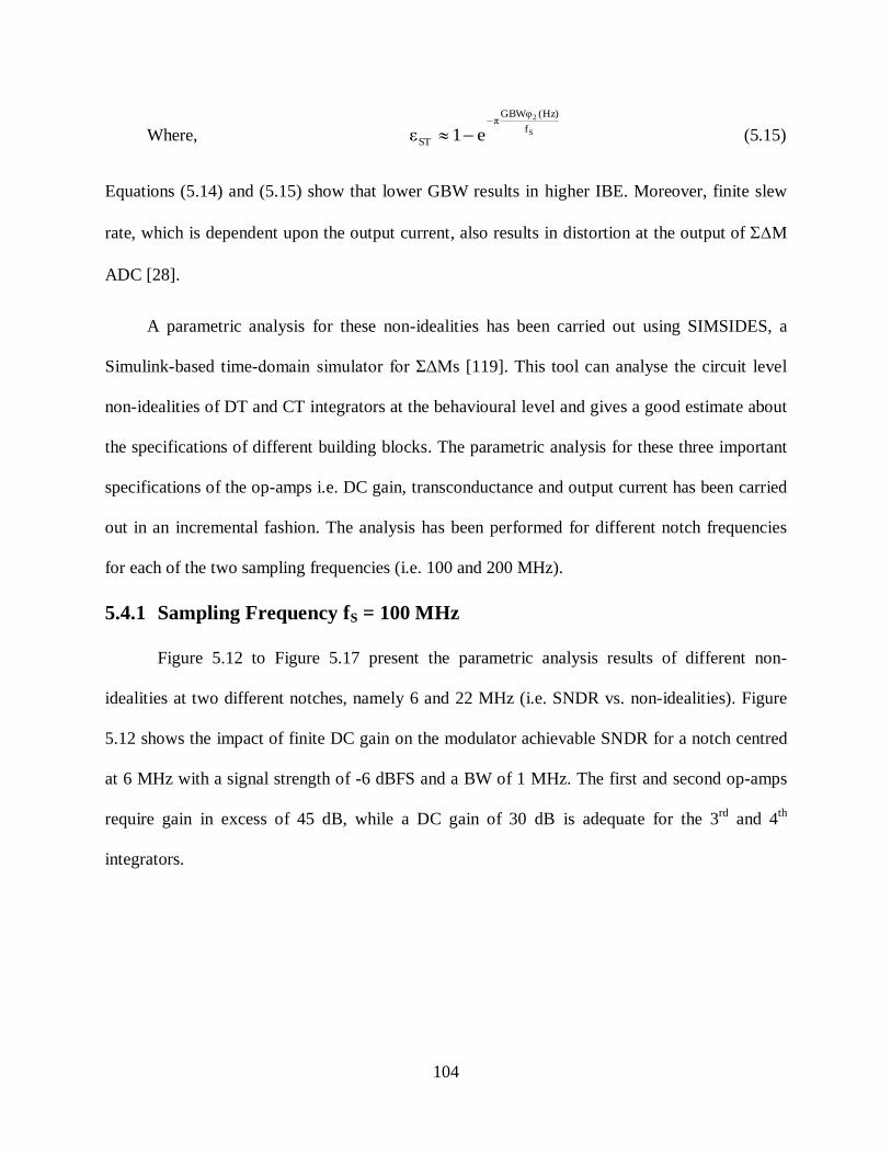
104
Where, S
2
f
(Hz)GBWυπ
ST e1ε
(5.15)
Equations (5.14) and (5.15) show that lower GBW results in higher IBE. Moreover, finite slew
rate, which is dependent upon the output current, also results in distortion at the output of M
ADC [28].
A parametric analysis for these non-idealities has been carried out using SIMSIDES, a
Simulink-based time-domain simulator for ΣΔMs [119]. This tool can analyse the circuit level
non-idealities of DT and CT integrators at the behavioural level and gives a good estimate about
the specifications of different building blocks. The parametric analysis for these three important
specifications of the op-amps i.e. DC gain, transconductance and output current has been carried
out in an incremental fashion. The analysis has been performed for different notch frequencies
for each of the two sampling frequencies (i.e. 100 and 200 MHz).
5.4.1 Sampling Frequency fS = 100 MHz
Figure 5.12 to Figure 5.17 present the parametric analysis results of different non-
idealities at two different notches, namely 6 and 22 MHz (i.e. SNDR vs. non-idealities). Figure
5.12 shows the impact of finite DC gain on the modulator achievable SNDR for a notch centred
at 6 MHz with a signal strength of -6 dBFS and a BW of 1 MHz. The first and second op-amps
require gain in excess of 45 dB, while a DC gain of 30 dB is adequate for the 3rd
and 4th
integrators.

105
Figure 5.12. SNDR vs. DC gain (fN = 6 MHz, fN = 100 MHz).
After adjusting the DC gains of the all 4 op-amps to 46 dBs, a parametric analysis has
been performed for the transconductance, (see Figure 5.13). The first and second op-amps
require a higher transconductance (in the range of 4-to-5 mA/V). While, 3rd
and 4th
op-amps
require a transconductance in the region of 3 mA/V. Employing the same methodology as
mentioned above, a parametric analysis has been performed for the output current. Figure 5.14
shows the corresponding result.
Same parametric analysis for these three specifications was also completed with fN of 22
MHz. Figure 5.15 to Figure 5.17 depict the corresponding results. These figures illustrate that the
op-amps specifications become much more demanding for higher notch frequencies. If the op-
amps can cope with the required specifications of higher notches, the lower frequency
requirements are automatically met. Therefore, the specifications of op-amps have been tuned to
operate correctly at 22 MHz. Table 5.6 details the selected parameters, determined using the
above-mentioned criteria. Table 5.7 depicts the SNDR signals with different bandwidth at two
different notch frequencies with the selected parameters of op-amps for an input of -6 dBFS.

106
Figure 5.13. SNDR vs. transconductance (fN = 6 MHz, fN = 100 MHz).
Figure 5.14. SNDR vs. output current (fN = 6 MHz, fN = 100 MHz).
Figure 5.15. SNDR vs. DC gain (fN = 22 MHz, fN = 100 MHz).

107
Figure 5.16. SNDR vs. transconductance (fN = 22 MHz, fN = 100 MHz).
Figure 5.17. SNDR vs. output current (fN = 22 MHz, fN = 100 MHz).
Table 5.6. Op-amps specifications (fs = 100 MHz).
First
op-amp
Second
op-amp
Third
op-amp
Fourth
op-amp
DC Gain (dB) 46.9 46.9 46.5 45.6
gm (mA/V) 4.2 4.1 3.2 1.5
Io (mA) 0.50 0.90 0.60 0.50
o/p swing for 22MHz (V) ±0.18 ±0.13 ±0.07 ±0.08
o/p swing for 6MHz (V) ±0.26 ±0.36 ±0.37 ±0.25
Input cap. (fF) 72 72 72 72
Output cap. (fF) 32 32 32 32
Eq. input noise
(nV/Hz1/2
)
4 4 5 8

108
Table 5.7. SNDR for different bandwidths (fs = 100 MHz).
Notch Frequency (MHz)
Bandwidth (MHz)
SNDR (dB)
6
2.00 59.84
1.00 70.48
0.50 81.89
0.20 85.87
22
2.00 57.64
1.00 69.12
0.50 78.40
0.20 80.20
5.4.2 Sampling Frequency fS = 200 MHz
Following the same procedure as mentioned in section 5.4.1 , a parametric analysis has
been carried out for fS = 200 MHz. The results for two different notch frequencies of 30 and 36
MHz are illustrated in Figure 5.18 to Figure 5.23
Figure 5.18. SNDR vs. DC gain (fN = 30 MHz, fS = 200 MHz).

109
Figure 5.19. SNDR vs. transconductance (fN = 30 MHz, fS = 200 MHz).
Figure 5.20. SNDR vs. output current (fN = 30 MHz, fS = 200 MHz).
Figure 5.21. SNDR vs. DC gain (fN = 36 MHz, fS = 200 MHz).

110
Figure 5.22. SNDR vs. transconductance (fN = 36 MHz, fS = 200 MHz).
Figure 5.23. SNDR vs. output current (fN = 36 MHz, fS = 200 MHz).
Table 5.8 gives the resultant required parameters for op-amps while Table 5.9 shows the SNDR
for the different bandwidths and notches for an input of -6 dBFS.
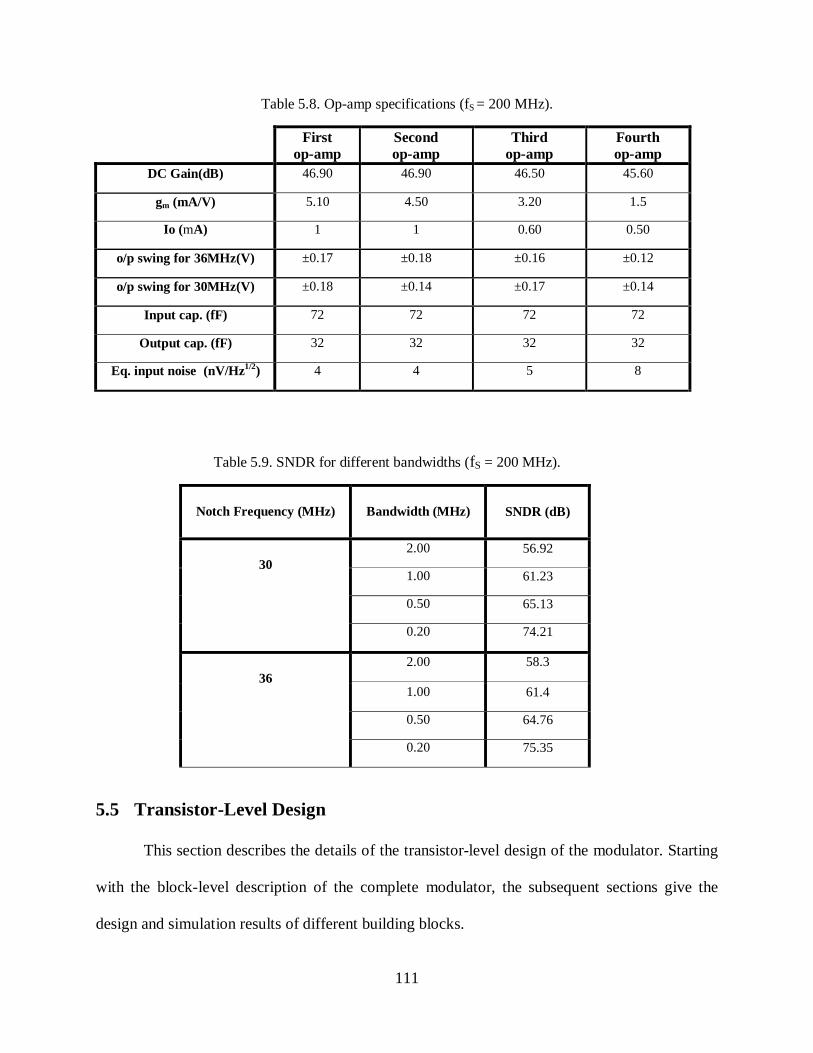
111
Table 5.8. Op-amp specifications (fS = 200 MHz).
First
op-amp
Second
op-amp
Third
op-amp
Fourth
op-amp
DC Gain(dB) 46.90 46.90 46.50 45.60
gm (mA/V) 5.10 4.50 3.20 1.5
Io (mA) 1 1 0.60 0.50
o/p swing for 36MHz(V) ±0.17 ±0.18 ±0.16 ±0.12
o/p swing for 30MHz(V) ±0.18 ±0.14 ±0.17 ±0.14
Input cap. (fF) 72 72 72 72
Output cap. (fF) 32 32 32 32
Eq. input noise (nV/Hz1/2
) 4 4 5 8
Table 5.9. SNDR for different bandwidths (fS = 200 MHz).
Notch Frequency (MHz)
Bandwidth (MHz)
SNDR (dB)
30
2.00 56.92
1.00 61.23
0.50 65.13
0.20 74.21
36
2.00 58.3
1.00 61.4
0.50 64.76
0.20 75.35
5.5 Transistor-Level Design
This section describes the details of the transistor-level design of the modulator. Starting
with the block-level description of the complete modulator, the subsequent sections give the
design and simulation results of different building blocks.

112
5.5.1 SC Implementation of Modulator
A single-ended SC implementation of the modulator is given in Figure 5.24. This
diagram represents the arrangement of 4 integrators, an active adder, quantiser and the feedback
DAC. The sampling capacitors in front of each integrator are represented by Csb1, Csc2, Csc3 and
Csc4. The first sampling capacitor Csb1, has been divided into 4 parts to realise a 5 level feedback
[58]. Ci1 to Ci4 are the integrating capacitors for the integrators. The sampling capacitors of the
adder are represented by Csb5, Csa2, Csa2, Csa3 and Csa4. Moreover, Csg1 and Csg2 are the capacitors
to realise the resonance.
All the integrators and adder employ the variable sampling capacitors to realise the
desired capacitor ratio listed in Table 5.10.

113
-+
+-
P1
N1
Ø1
d
Ø2
Vip
Vref-
Vref+
Ø1
Csb
1 /4
P4
N4
Vref-
Vref+
Ci1
-+
+Ø
1
Ø1
d
Csc
2
Ci2
Ø2
Ø2
d
-
-+
+-
Ø1
Ø1
dC
sc3
Ci
3
Ø2
Ø2
d
-+
Ø1
Ø1
d
Ci4
Ø2
Ø2
d
-+
+-Ø
1
Csa
4
Cia
Ø2
Ø1
d
Ø2
d
Ø1
Csa
3
Ø2
Ø1
d
Ø2
d
Ø1
Csa
2
Ø2
Ø1
d Ø2
d
Ø1
Csa
1
Ø2
Ø2
d
Ø1
Csb
5
Ø2
Ø2
d
Ø1
d
Csb
1 /4
Ø1
d
Ø1
Ø2
Csg
1Ø
2d
Ø1
d
Ø1
Ø1
d
Csg
2
Ø2
Ø2
d
Ø1
d1
.d5
d1
.d5
PD
3L
RO
MY
1 .Y
3
d1
.d5
P1
P2
P3
P4
N1
N2
N3
N4
DA
C
Csc
4
+-
Figure 5.24. Single-ended version of a 4th-order SC M.

114
Table 5.10. Implementation of integrator coefficients.
Coefficient Capacitor Ratio Coefficient Capacitor Ratio
a1 ia
sa1
C
C
c1 i1
sc1
C
C
a2 ia
sa2
C
C
c2 i2
sc2
C
C
a3 ia
sa3
C
C
c3 i3
sc3
C
C
a4 ia
sa4
C
C
c4 i4
sc4
C
C
b1 i1
sb1
C
C
g1 i1
sg1
C
C
b5 ia
sb5
C
C
g2 i2
sg2
C
C
The first integrator coefficient (i.e. b1) remains the same over the full range of fN.
Therefore, its sampling capacitor is fixed. The remaining integrators and adder employ variable
sampling capacitors. As an illustration, Figure 5.25 depicts the single-ended version of the 3rd
integrator. Here the integrating capacitor remains fixed while sampling and the resonant
capacitors are made up of binary weighted capacitors (Csc3 is made up of Cuc1, Cuc2, Cuc3 and Cuc4
while Csg2 is made up of Cug1, Cug2, Cug3, Cug4 and Cug5). Depending upon the control signal, the
binary weighted sampling capacitors can be added or removed from the circuit to realise the
desired ratio with integrating capacitor (and hence the coefficient) [123]. With this approach, the
capacitor ratio to implement a loop filter coefficient for a specific notch is achieved. The
resonance capacitors, Csg1 and Csg2, are more sensitive to the parasitic. Therefore, a simpler

115
configuration has been adopted for their implementation (as shown in Figure 5.26). Here the
binary weighted capacitors branches are connected and disconnected using a single switch
connected in series.
Ø2
D3 D2 D1 D0
out2p
Cuc1
Cuc2
Cuc3
Cuc4
Ø1
out3p-
+
Ø2
d
Ø1
doutp4
Ø1d
Ø2d
_D
0
_D1_D2_D3
_D1_D2_D3
D3D2 D1 D0
Ci3
Ø2
Ø1
Cug4
Cug3
Cug2
Cug1
Cug5
D0
Figure 5.25. Switched capacitor implementation of the third integrator.
Cug4
Cug3
Cug2
Cug1
Cug5
Figure 5.26. Implementation of variable resonance capacitor (Csg1 and Csg2).

116
5.5.2 Op-Amps
Due to the higher output swing, good stability and larger gain, a folded cascode topology
has been adopted for all of the op-amps in the modulator [1]. The circuit diagrams of the op-amp
and common-mode feedback network employed are shown in Figure 5.27 (a) and (b),
respectively. To reduce the substrate noise coupling, the differential input pair uses the PMOS
transistors. Minimum-length transistors have been avoided in the input pair and in the current
mirrors in order to reduce the 1/f noise and mismatch effects. Table 5.11 and Table 5.12
summarise the transistor sizes and achievable performance of the op-amp with the different bias
current settings.
IN-NM2
M3
IN-P
M1
M4M5
M6M7
M8M9
M11M10
M6B
M6BPM8BP
M8BN
M11B
M4B
B
A
MBias
(a)
BBA
Vo+
Vo-
Φ2
Φ2
Φ2
Φ2
Φ1
Φ1
Φ1
Φ1
(b)
Figure 5.27. Folded cascode op-amp: (a) Core op-amp (b) SC common-mode feedback network.

117
Table 5.11. Transistor sizes of op-amp.
Length (μm) Width (μm)
M1, M2 0.25 264.08
M3 0.4 276
M4, M5 1 233.8
M6 0.2 23.52
M8BP, M9, M11B 0.2 50
M10, M11 0.4 184
M3B, M6BP 0.4 23
M4B, M8BN 1 16.7
M6B 0.955 1.65
M8B 0.99 3.72
Table 5.12. Op-amp performance summary.
Bias Current (μA) 10 20 30 40 50 60 65 70
DC gain (dB) 47.33 47.77 47.77 47.45 46.9 46.21 45.7 45.31
gm (mA/V) 1.56 1.45 2.45 3.60 4.01 4.58 5.20 5.48
Phase margin 62.20 63.30 63.55 64.10 64.20 64.40 64.50 64.60
Io (μA) 87.2 185.70 286.60 389.00 491.00 596.00 647.00 698.00
Output swing (V) ±0.9 ±0.8 ±0.73 ±0.67 ±0.61 ±0.56 ±0.53 ±0.50
Input cap. (fF) 322 320 332 343 347 354 359 362
Output cap. (fF) 28 27 23 20 18 17 16 15
Power (mW) 0.64 1.17 1.80 2.03 2.50 2.95 3.14 3.37
5.5.3 Capacitors
Due to the better capacitor density and lower cost, MOM capacitors have been used in all
the integrators and adder. These capacitors rely on the coupling capacitance between the
interdigitated metal fingers as shown in Figure 5.28. The metal fingers can be stacked to increase
the capacitance density. Another benefit associated with MOM capacitors is lower bottom-plate
parasitic capacitance (less than 5 %) compared to the standard MIM capacitors.
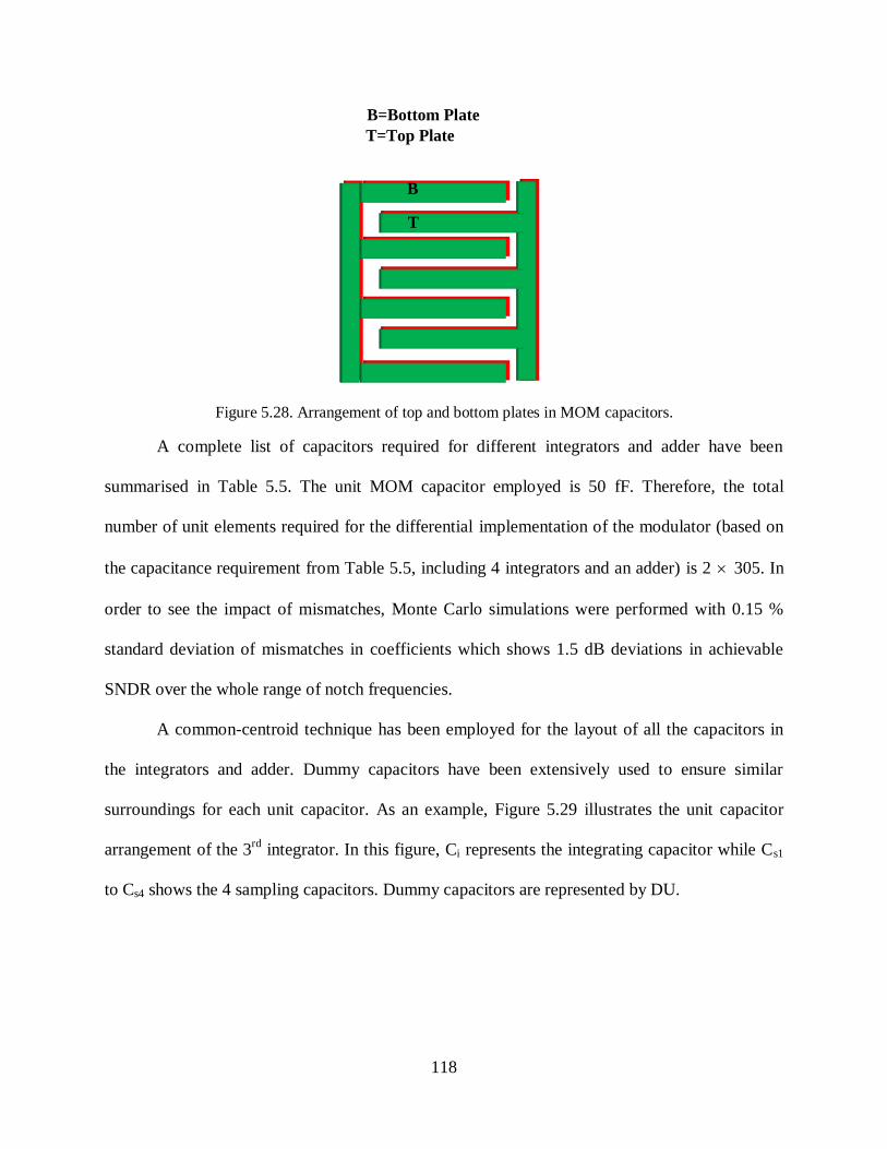
118
B
B=Bottom Plate
T=Top Plate
T
Figure 5.28. Arrangement of top and bottom plates in MOM capacitors.
A complete list of capacitors required for different integrators and adder have been
summarised in Table 5.5. The unit MOM capacitor employed is 50 fF. Therefore, the total
number of unit elements required for the differential implementation of the modulator (based on
the capacitance requirement from Table 5.5, including 4 integrators and an adder) is 2 305. In
order to see the impact of mismatches, Monte Carlo simulations were performed with 0.15 %
standard deviation of mismatches in coefficients which shows 1.5 dB deviations in achievable
SNDR over the whole range of notch frequencies.
A common-centroid technique has been employed for the layout of all the capacitors in
the integrators and adder. Dummy capacitors have been extensively used to ensure similar
surroundings for each unit capacitor. As an example, Figure 5.29 illustrates the unit capacitor
arrangement of the 3rd
integrator. In this figure, Ci represents the integrating capacitor while Cs1
to Cs4 shows the 4 sampling capacitors. Dummy capacitors are represented by DU.
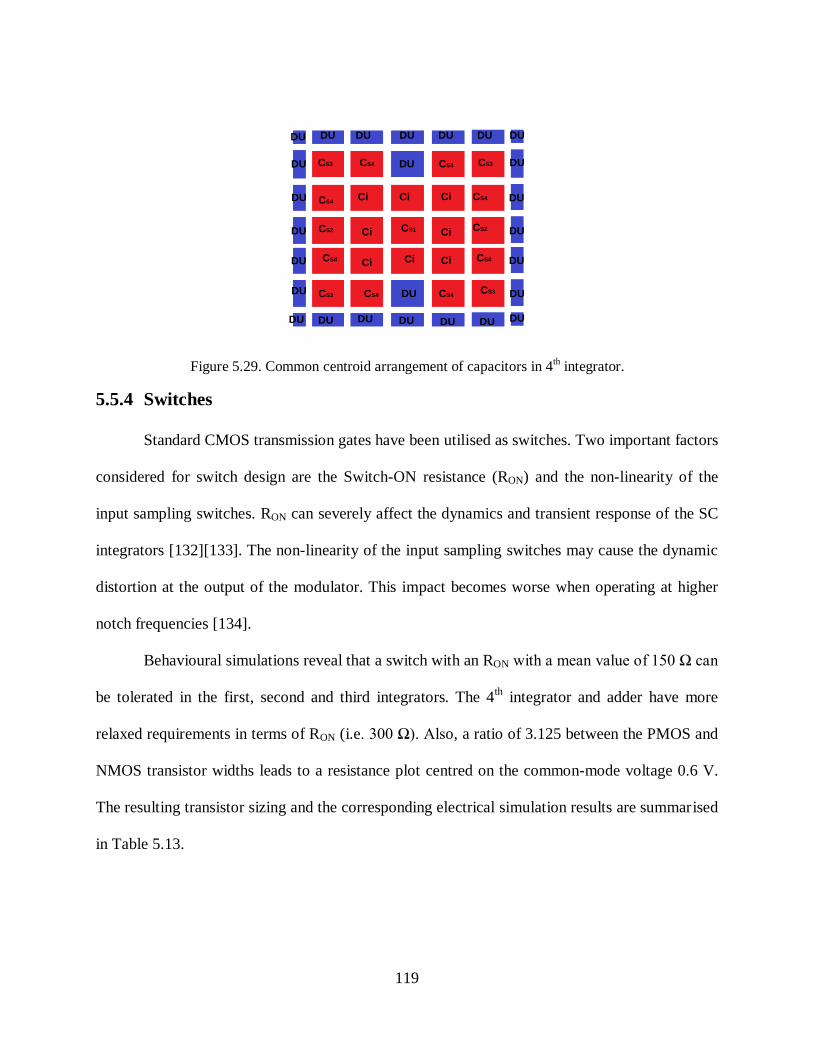
119
DU
DU
DU
DU
DU
DU
DU DU DU DU DU DU DU
DU
DU
DU
DU
DU
DUDU DU DU DUDU
DU
DUCS4 CS4
CS4 CS4
CS4
CS4 CS4
CS4
CS3CS3
CS3CS3
CS2 CS2CS1
CiCiCi
Ci
Ci Ci
Ci
Ci
Figure 5.29. Common centroid arrangement of capacitors in 4th integrator.
5.5.4 Switches
Standard CMOS transmission gates have been utilised as switches. Two important factors
considered for switch design are the Switch-ON resistance (RON) and the non-linearity of the
input sampling switches. RON can severely affect the dynamics and transient response of the SC
integrators [132][133]. The non-linearity of the input sampling switches may cause the dynamic
distortion at the output of the modulator. This impact becomes worse when operating at higher
notch frequencies [134].
Behavioural simulations reveal that a switch with an RON with a mean value of 150 Ω can
be tolerated in the first, second and third integrators. The 4th integrator and adder have more
relaxed requirements in terms of RON (i.e. 300 Ω). Also, a ratio of 3.125 between the PMOS and
NMOS transistor widths leads to a resistance plot centred on the common-mode voltage 0.6 V.
The resulting transistor sizing and the corresponding electrical simulation results are summarised
in Table 5.13.

120
Table 5.13. Transistor sizing of switches of the different integrators and adder.
First, Second and Third
Integrator
4th
Integrator Adder
Width
PMOS (μm)
12 6
Width
NMOS (μm)
3.84 1.92
Length
PMOS, NMOS (nm)
80 80
RON (Ω) 147 285
Cdd (fF)
Css (fF)
30.63
15.46
5.5.5 Comparators
Dynamic comparator architecture composed of three blocks, pre-amplifier, regenerative
latch and set-reset (SR) latch, has been utilised in the modulator. This comparator presents very
appealing features of high-speed, low power consumption and low offset. Figure 5.30 (a) and (b)
presents the schematics of the pre-amplifying stage and the regenerative latch of the comparator,
respectively.
IN-NM1 M2
M3 M4
VREFN IN_P VREFNP
X-PX-N
M5 M6M7
S
M9 M10
M12 M13
M9 M11
M15M14strb
strb
strb
strb
R
(a) (b)
Figure 5.30.Comparator schematic (a) Pre-amplifying stage (b) Regenerative latch.

121
5.5.6 Quantiser
The quantiser has a differential flash architecture and can be divided into three parts as
depicted in Figure 5.31 [135]. First part consists of a resistor ladder generating the voltage
references for individual comparators while the second part consists of an array of comparators
that compares the adder output with the reference voltages generated in the resistor ladder. The
third part of ADC consists of digital logic that translates the thermometer code at the output of
comparators. The delays of all the digital paths are balanced with buffers (not shown in the
figure).
V+ rc1,5L
V+ rc2,5L
Vr-
Vr+
15 RES
15 RES
30 RES
30 RES
30 RES
V- rc1,5L
V- rc2,5L
V+ rc1,5L
V- rc1,5L
V+ rc2,5L
V- rc2,5L
V- rc2,5L
V+ rc2,5L
V+ rc1,5L
V- rc1,5L
Vi-Vi+
VDDDD
_Φ1
_Φ1
_Φ1
_Φ1
d4
d3
d2
d1
d0
PD5L
PD3L
Resistance Ladder ComparatorsDigital Logic
Figure 5.31. Resistance ladder, quantiser and digital logic.
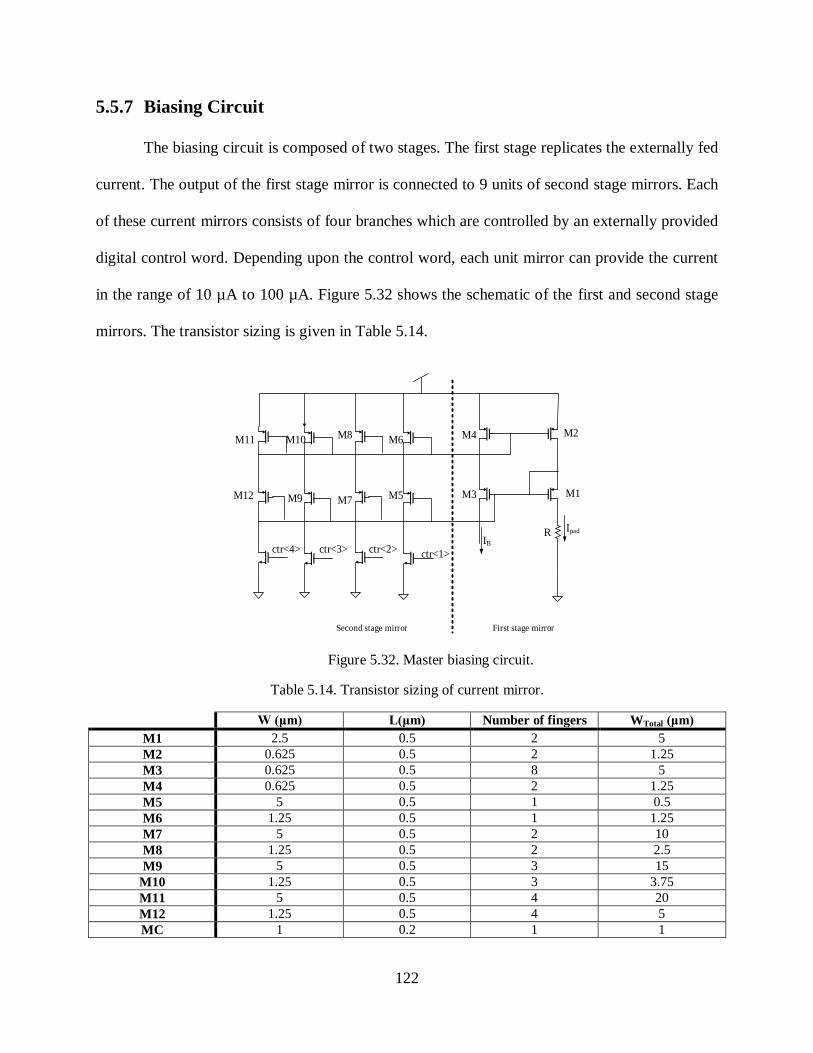
122
5.5.7 Biasing Circuit
The biasing circuit is composed of two stages. The first stage replicates the externally fed
current. The output of the first stage mirror is connected to 9 units of second stage mirrors. Each
of these current mirrors consists of four branches which are controlled by an externally provided
digital control word. Depending upon the control word, each unit mirror can provide the current
in the range of 10 µA to 100 µA. Figure 5.32 shows the schematic of the first and second stage
mirrors. The transistor sizing is given in Table 5.14.
M9
ctr<1> ctr<2> ctr<3> ctr<4>
R Ipad
M1
M2
M3
M4
M5
M6
M7
M8M10M11
M12
IB
First stage mirror Second stage mirror
Figure 5.32. Master biasing circuit.
Table 5.14. Transistor sizing of current mirror.
W (μm) L(μm) Number of fingers WTotal (μm)
M1 2.5 0.5 2 5
M2 0.625 0.5 2 1.25
M3 0.625 0.5 8 5
M4 0.625 0.5 2 1.25
M5 5 0.5 1 0.5
M6 1.25 0.5 1 1.25
M7 5 0.5 2 10
M8 1.25 0.5 2 2.5
M9 5 0.5 3 15
M10 1.25 0.5 3 3.75
M11 5 0.5 4 20
M12 1.25 0.5 4 5
MC 1 0.2 1 1
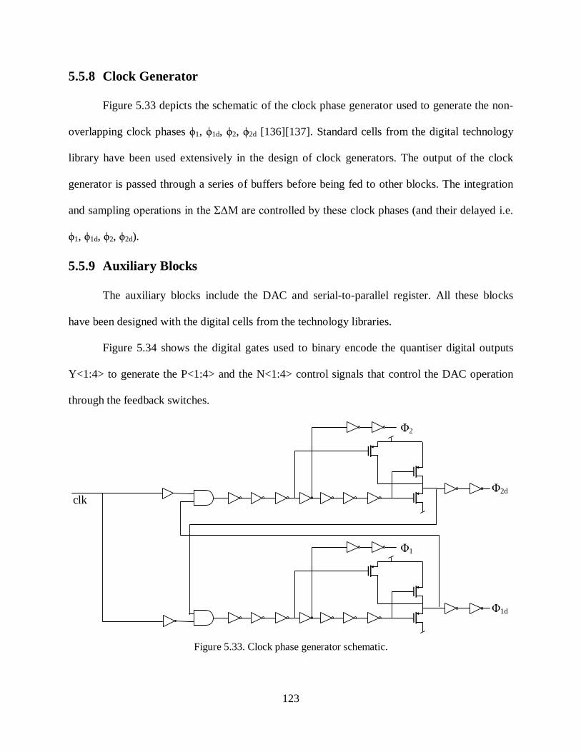
123
5.5.8 Clock Generator
Figure 5.33 depicts the schematic of the clock phase generator used to generate the non-
overlapping clock phases ϕ1, ϕ1d, ϕ2, ϕ2d [136][137]. Standard cells from the digital technology
library have been used extensively in the design of clock generators. The output of the clock
generator is passed through a series of buffers before being fed to other blocks. The integration
and sampling operations in the ΣΔM are controlled by these clock phases (and their delayed i.e.
ϕ1, ϕ1d, ϕ2, ϕ2d).
5.5.9 Auxiliary Blocks
The auxiliary blocks include the DAC and serial-to-parallel register. All these blocks
have been designed with the digital cells from the technology libraries.
Figure 5.34 shows the digital gates used to binary encode the quantiser digital outputs
Y<1:4> to generate the P<1:4> and the N<1:4> control signals that control the DAC operation
through the feedback switches.
Φ2
Φ2d
Φ1
Φ1d
clk
Figure 5.33. Clock phase generator schematic.

124
Φ2
Y<1>P<1>
Φ2
Y<2>P<2>
Φ2
Y<3>P<3>
Φ2
Y<4>P<4>
Φ2
_Y<1>N<1>
Φ2
_Y<2>N<2>
Φ2
_Y<3>N<3>
Φ2
_Y<4>N<4>
Figure 5.34. DAC control signals configuration.
The reconfiguration of the modulator coefficients and biasing requires a specific
combination of control signals. In order to cope with this, a serial-to-parallel register is used
[135]. It is designed by connecting several (76) D flip-flops in series, this register can be loaded
with a specific control word (used to realise the specific SC ratios and biasing etc.). The block
diagram of the register is depicted in Figure 5.35.
76 Bit Serial Shift Register
76 Bit Parallel Load Register
In
Load
Clock
Out Serial
O1O2O76Parallel Outputs
Figure 5.35. Block diagram of the serial-in parallel-out register.

125
The clock signal, “Clock”, functions as the input clock for the flip-flops of the register in
the serial shift register block. While another input signal, “Load”, enables either the shifting
operation in the top register or the loading in the bottom register, as illustrated in Figure 5.35.
The serial input data, “In”, is collected and transformed into 76 parallel control bits, “O1-O76”.
Table 5.15. Functionality of control signals.
.
Index
Signal name
Description
1..4 ctr_biasCM<1:4> Biasing of CM
5..8 ctr_oa1<1:4> Biasing of first op-amp
9:12 ctr_oa2<1:4> Biasing of second op-amp
13..16 ctr_oa3<1:4> Biasing of third op-amp
17..20 ctr_oa3<1:4> Biasing of fourth op-amp
21..24 ctr_add<1:4> Biasing of Adder
25..28 ctr_comp<1:4> Biasing of comparator
29..32 ctr_test<1:4> Biasing of test circuit
33 PD3L 3 Level quantiser activation
34 PD5L 5 Level quantiser activation
36 PD_gen Quantiser master enable
37..41 D_g1<1:5> First resonance
42..45 D_int2<1:4> Second integrator sampling
46..50 D_g1<1:5> Second resonance
51..54 D_int3<1:4> Third integrator sampling
55..58 D_int4<1:4> Fourth integrator sampling
59..63 D3<1:5>
Adder control 64..68 D4<1:5>
69..73 D5<1:5>
74..76 SIG_CON<3:5>

126
5.6 Layout Design
Figure 5.36 illustrates the layout of the M where the different blocks are highlighted.
1st I
nte
gra
tor
2n
d In
teg
rato
r
3rd
In
teg
rato
r
4th
In
teg
rato
r
Ad
de
r
Qu
an
tize
r
STP RegisterMaster BiasD
igita
l P
art
I/O
Rin
g
An
alo
g P
art
I/O
Rin
g
Mixed Part I/O Ring
Figure 5.36. Layout of whole M ADC with different blocks being highlighted.

127
Depending upon the switching activity and functionality, the whole modulator can be
considered as made up of three different sections. The analog section consists of the op-amps,
capacitors, pre-amplifiers of the comparators and the master bias circuitry. The mixed-signal
section consists of switches (of the integrators and the analog adders), the regenerative latches of
the comparators and the buffers of the clock phases. The digital section consists of the digital
gates, ROM, the digital logic of DAC and serial-to-parallel register. All these sections are
provided with distinct power and ground supplies from the I/O ring. In order to avoid noise
coupling that result from bulk sharing, guard rings have been employed across these three
sections.
The I/O ring consists of two types of cells. Full custom cells are used for the analog and
mixed signals and power supplies. High speed digital signals e.g. control bits, clocks and digital
output bit stream use the I/O cells from the digital library. The fast switching part of the I/O ring
is placed as far as possible from the other sections. In order to avoid the switching coupling
noise, the analog and the mixed signals part of the ring is physically separated from the digital
part of the I/O ring, as shown in Figure 5.36.
5.7 Experimental Characterization
The ADC is fabricated in a 90-nm 1P8M CMOS 1.2 V process and has an area of 3.515
mm2 (1875m 1875m). A micrograph of ADC is shown in Figure 5.37 .

128
Figure 5.37. Micrograph of the fabricated ADC.

129
5.7.1 Test PCB
The test printed circuit board (PCB) schematic is shown in Figure 5.38 and a photograph
is depicted in Figure 5.39. The following considerations highlight some of the test PCB aspects:
1. The input signal is generated from an external source (fully differential low-distortion
external source Tektronix SG5010 audio oscillator) and provided to the PCB via an SMA
connector. After being applied, the input signal is filtered by a passive RC antialiasing
filter on the PCB. A set of capacitors and 50 Ω resistors are used to realise this filtering
function.
2. The PCB applies the external voltage of a 2.5 V supply required for the I/O devices and a
1.2 V supply required for the internal circuitry of the chip.
3. The CM voltage is generated on chip but there is also provision to apply an external CM.
To this purpose, a buffer and the footprint of a 0 Ω resistor has been included on the
PCB.
4. All the on-chip supplies, references etc. are passed through the passive low-pass ᴨ filters
mounted on the PCB before their connection with the chip. Each ᴨ filter consists of two
capacitors and one inductor.
5. Different jumpers, test points and 0 Ω resistors have been extensively mounted over the
whole PCB to measure the currents and voltages at different test points.
6. Decoupling capacitors have been used between all the power supplies, references,
grounds, and CM etc.
7. There is also a provision for the logic-analyser connection that is used to collect the
output bit stream for the processing.
8. The PCB has 4 layers with separate ground and power planes.

130
CO
N_
GN
D
CO
N_
+2
.5V
CO
N_
-2.5
V
L0
1
H
C0
10
F
C1
10
F
C2
10
F
R
10
C2
7
10
F
L3
1
H
L4
1
H
L5
1
H
L6
1
H
L7
1
H
L8
1
H
L9
1
H
L1
0 1
H
C3
4
100
nF
C3
2 10
F
C3
1 10
F
C3
0 10
F
C2
9 10
F
C2
8 10
F
C2
7 10
F
C2
6 10
F
VSSAA
VSSmix
VSSGAD
VSS25buff
VSSAD
VSS25V
VPH_B US
VSSADB uff
C3
5
100
nF
C3
6
100
nF
VD
DA
AR
EF
VD
DA
AR
EF
VS
SA
A
TP
-GN
D1
TP
-GN
D2
R 2
1
50
R 2
3
50
R 2
8
50
R 3
0
50
TP
15
TP
17
TP
20
VD
A2
5
OP
204
CM
OU
T
R2
7 0
567
32
1O
P 2
64
VD
A2
5
R2
7 2.2
R2
9 4
C4
3
10
R4
2 2.2
R2
8 4
C4
1 10
C3
0 100
n
R2
7 2.2
R2
9
4
C4
3
10
C3
0 100
n
VR
EF
-EX
T+
CM
-EX
T
VS
SA
AV
SS
AA
VS
SA
A
VS
SA
A
VR
EF
-EX
T-
VS
SA
AV
SS
AA
TP
13
TP
18
TP
21
OP
265
VD
A2
5
VS
S2
5
VD
D2
5
R2
2
50
R2
6
50
J_C
LK
J_T
RG
_A
UX
TR
G_
AU
X
CL
K
1 2
J-GN
D
C4
10n
F
C5
1p
F
C0
100
pF
C7
100
pF
C1
4
10n
F
C1
5
1n
F
C1
6
100
pF
C2
3
100
nF
C2
4
100
nF
C2
5
100
nF
C2
6
100
nF
C2
2
100
nF
VD
DA
AD
buff
VS
SA
Db
uff
VD
DA
AV
SS
AA
VD
D2
5
VS
S2
5
VD
DD
D
VS
SD
D
VD
D1
2
VS
S1
2
C1
1
10n
F
C1
2
1n
F
C1
3
100
pF
C2
100
nF
C3
10n
F
C1
9
100
nF
C2
0
10n
F
C2
1
10n
F
12
3
4
CM
-EX
T
R2
50
R5
50
CW
1
50p
F
R3
50
R6
50
R4
0
R70
JR1
JR-IN
T1
46
12 3
R3
3 0
R3
4 0
R3
5 0
CM
-EX
T
VS
SA
A
RE
F-E
XT
+
CM
-OU
T
CM
-EX
T
VD
DA
A
RE
F-E
XT
-
R8
0
R9
0
R1
0 0
R1
1 0
R1
2 0
R1
3 0
IN+
IN-
RE
F+
RE
F-
CM
S+
S-
TP
11
S+
S-
TP
13
R1
4
10K
C3
4
100
nR
16
10K
C3
7
100
n
VSSAA
VSSAA
VSSAA
VSSAA
424
3
44
40
45
38
23
VSSAA
VSSAA
VSSAA
VSSAA
VSSmix
VSSmix
VSSADbuff
VSSADbuff
VSSDD
VSSGD
VSS12
VSS25
VSS25
37
25
22
29
34
38
52
55
53
49
56
40
42
2
6
10 BIT
1
BIT
2
BIT
3
CL
K
TR
IGG
ER
CL
K_
IN
EN
AB
LE
_IN
DA
TA
_IN
RE
G_
OU
T
678315
11
12
13
14
6
7
8
3
15
11
12
13
14
VDDGD
VDDAA (2)
VDDAA (3)
VDDAA (4)
VDDAA (5)
VDDmix(1)
VDDmix (2)
VDDADbuff
VDDDD
VDD12
VDD25(1)
VDD25(2)
VDDGD
VDDAA
VDDAA
VDDAA
VDDAA
VDDmix
VDDmix
VDDADbuff
VDDDD
VDD12
VDD25
VDD25
VSSAA
VSSAA
VSSAA
VSSAA
VSSmix
VSSmix
VSSADbuff
VSSDD
VSSGD
VSS12
VSS25
VSS25
BIT
1
BIT
2
BIT
3
CL
K
TR
IGG
ER
CL
K_
IN
EN
AB
LE
_IN
DA
TA
_IN
RE
G_
OU
T
531 97 15
13
11
19
17
25
23
21 29
27
35
33
31 37
642 108 16
14
12
20
18
26
24
22 30
28
36
34
32
38
Pattern
Gen
erator fo
r CL
K_IN
,
DA
TA
_IN
, EN
AB
LE
_IN
531 97 15
13
11
19
17
642 108 16
14
12
20
18
CL
K_
IN
EN
AB
LE
_IN
DA
TA
_IN
xxxxxx xx
VD
D2
5b
uff
TP
10
PO
D_
EN
AB
LE
_IN
EN
AB
LE
_IN
SN
74A
UC
125
VD
D2
5b
uff
PO
D_
DA
TA
_IN
SN
74A
UC
125
DA
TA
_IN
VD
D2
5b
uff
VD
D2
5b
uff
PO
D_
CL
K_
IN
SN
74A
UC
125
TP
14
TP
16
CL
K_
IN
U4
D
Screw
holes
Auxiliary Pad
s
VD
D2
5b
uff
VS
S2
5b
uff
VD
D2
5
VS
S2
5
VD
DA
A
VS
SA
A
VD
Dm
ix
VS
Sm
ix
VD
D2
5
VS
S2
5
VD
DA
AR
EF
VS
SA
AR
EF
VD
D1
2
VS
S1
2
VD
DD
D
VS
SD
D
L1
1
H
L2
1
H
C2
7 10
F
C2
6 10
F
VD
DA
Db
uff
VS
SA
Db
uff
VD
DG
D
VS
SG
D
VS
SA
AR
EF
VD
DA
D
VS
SA
D
VSSmix VSSmix
VSS25
VSS12
VSSDD
CL
K
TR
IG
TR
IG_
AU
X
VSSADbuff
C3
3 10
F
L1
2 1
H
VSSDD
C4
2
100
n
VD
D2
5
VS
S2
5
BIT
1
BIT
2
BIT
3
CL
K
TR
IGG
ER
RE
G_
OU
T
TR
Ig_
AU
X
TP
1T
P6
TP
12
TP
14
R5
5 0
R5
6 0
R5
7 0
Deco
up
ling
Cap
acito
r
Lo
gic
Analy
ser Conn
ector
Gro
un
d D
ivisio
n
Su
pp
lies π F
ilterin
g
Figure 5.38. Test PCB for the evaluation of the ADC.

131
Figure 5.39. Photograph of the test PCB.
5.7.2 Experimental Results
The experimental verification of the 4th-order DT CRFF-based M has been carried out
over the various notch frequencies. In the first step of the characterization plan, a pre-selected
control word (generated by pattern generator) is loaded into the serial-to-parallel register of the
ADC. This control word sets the reconfigurable coefficients and biasing of op-amps for a
particular notch. The same control word is available at one of the outputs of M to verify that it
has been loaded accurately. Once the control word is correctly written to the register, an input
tone can then be applied. By using single tones of different frequencies and strengths, the
modulator performance has been validated. The output of the modulator consists of a 3-bit word
that is captured by the logic analyser and subsequently processed in Matlab®.
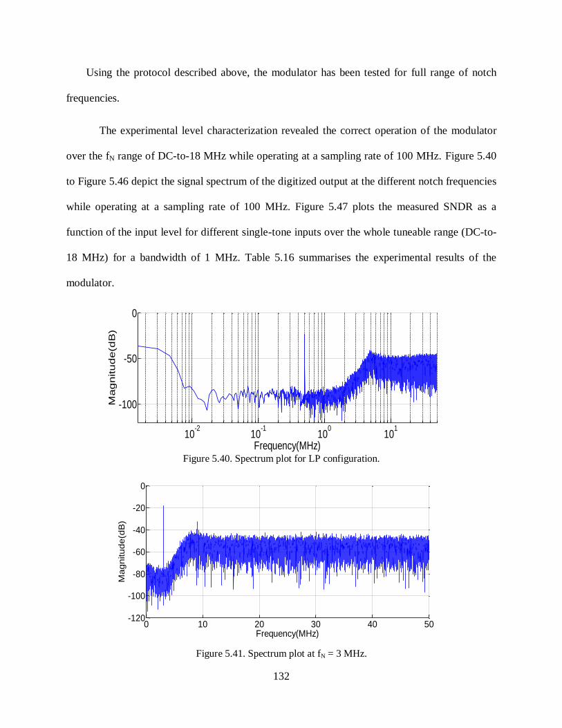
132
Using the protocol described above, the modulator has been tested for full range of notch
frequencies.
The experimental level characterization revealed the correct operation of the modulator
over the fN range of DC-to-18 MHz while operating at a sampling rate of 100 MHz. Figure 5.40
to Figure 5.46 depict the signal spectrum of the digitized output at the different notch frequencies
while operating at a sampling rate of 100 MHz. Figure 5.47 plots the measured SNDR as a
function of the input level for different single-tone inputs over the whole tuneable range (DC-to-
18 MHz) for a bandwidth of 1 MHz. Table 5.16 summarises the experimental results of the
modulator.
Figure 5.40. Spectrum plot for LP configuration.
Figure 5.41. Spectrum plot at fN = 3 MHz.
10-2
10-1
100
101
-100
-50
0
Frequency(MHz)
Ma
gn
itu
de
(dB
)
0 10 20 30 40 50-120
-100
-80
-60
-40
-20
0
Frequency(MHz)
Ma
gn
itu
de
(dB
)

133
Figure 5.42. Spectrum plot at fN = 5 MHz.
Figure 5.43. Spectrum plot with fN = 6 MHz.
Figure 5.44. Spectrum plot at fN = 9 MHz.
0 10 20 30 40 50-120
-100
-80
-60
-40
-20
0
Frequency(MHz)
Ma
gn
itu
de
(dB
)
0 10 20 30 40 50-120
-100
-80
-60
-40
-20
0
Frequency(MHz)
Ma
gn
itu
de
(dB
)
0 10 20 30 40 50-120
-100
-80
-60
-40
-20
0
Frequency(MHz)
Ma
gn
itu
de
(dB
)
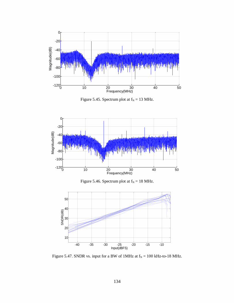
134
Figure 5.45. Spectrum plot at fN = 13 MHz.
Figure 5.46. Spectrum plot at fN = 18 MHz.
Figure 5.47. SNDR vs. input for a BW of 1MHz at fN = 100 kHz-to-18 MHz.
0 10 20 30 40 50-120
-100
-80
-60
-40
-20
0
Frequency(MHz)
Ma
gn
itu
de
(dB
)
0 10 20 30 40 50-120
-100
-80
-60
-40
-20
0
Frequency(MHz)
Ma
gn
itu
de
(dB
)
-40 -35 -30 -25 -20 -15 -10
10
20
30
40
50
Input(dBFS)
SN
DR
(dB
)

135
Table 5.16. Performance summary of the designed ADC
Process 90-nm
Active Area (mm2) 2.97
fS (MHz) 100
BW (MHz) 1
Notch Frequency (MHz) 0-to-18
Supply Voltage (V) 1.2
OSR 50
Peak SNDR (dB) 46-to-55
Power Consumption
Analog 10-13 mA
Mixed 7-8 mA
Digital 2-3 mA
Although the circuit level simulations revealed the correct operation of the modulator
over the whole range of notch frequencies, experimental level characterization have shown the
correct operation of modulator up to a fN of 18 MHz only while operating over a sampling rate of
100 MHz. Three possible reasons for the performance degradation are summarised in the
following.
1. Variable coefficients required for the fN tuneability, have been implemented with the
reconfigurable capacitor ratio, which are realised with the switched capacitor
branches. Parasitic capacitances introduced due to the routing and interconnection of
the capacitors disturb the capacitors ratio (or coefficients) resulting in the degradation
of the NTF. Due to unavailability of the layout-parasitic extractor for the design kit,
the parasitic impact was not fully evaluated at the post-layout level during the design
phase. Hence the routing and the interconnections were not optimised that led to the
degraded performance at experimental level.
2. The post-layout performance of the op-amps was not evaluated during the design
phase. Op-amps transconductance, DC gain and slew rate get degraded due to
parasitic. Transconductance requirements for the higher notch frequencies are much

136
higher. Therefore, the experimental level characterization has shown correct results up
to 18 MHz only while operating at 100 MHz. Moreover, due to the degraded DC gain,
zeros in the NTF are disturbed that causes increased noise in the signal band. As a
result, the achievable performance was lower than the expected.
3. No DEM has been implemented for 5 level feedback DAC. One consequence of this
can be observed in the simulated spectra (Figure 5.40 to Figure 5.46). The non-
linearity in the DAC caused the signal harmonics and higher in-band noise.
Table 5.17 compares the experimental results of the modulator with some other notable
examples of BP or reconfigurable LP/BP Ms. Compared to the previously reported SC-based
M ADCs ([123][138][139][140]) the designed ADC achieves a higher tuneability range. Over
the recent years, there has been a surge in CT implementations with tuneable notch. Three of the
notable recent continuous time implementations with a tuneable notch frequency are reported in
[96] [142] and [17]. The architecture reported in [96] employs a duty-cycle controlled DAC in
the feedback for better reconfiguration of notch frequency that can be varied over a range of 180-
to-220 MHz. [142] is a quadrature M and can achieve a notch tunability of 0.5-to-12 MHz.
The architecture detailed in [17] employs 3rd
order CT architecture that can operate in LP or BP
mode. Due to CT implementations of these three architectures, power consumption and hence
resultant FoMs are much lower. Another important architecture is [15]. This is a reconfigurable
architecture that can operate either in LP mode in BP mode. Also, a few reconfigurable receiver
architectures operating in GHz range featuring SC-based M ADCs have been reported
recently [89][145]. These architectures first down-convert the incoming signal using a variable
oscillation frequency and then a LP M ADC digitizes the baseband signal. The designed ADC
employs a single sampling frequency to digitize the range of input frequencies.

137
Table 5.17. Comparison of the designed ADC with other reported BP or reconfigurable BP M ADCs
Arch. fS (MHz) fN (MHz) BW
(MHz)
SNDR
(dB)
Power
(mW)
FoMW
(pJ/conv)
FoMS
(dB)
[138] SC 1 0.1-0.40 0.00781 61 200 13965 106.91
[123] SC 40 0-12.60 0.31 71-81 115 63-20 135.90-145
[139] SC 42.8 10.70 0.2 42.3 12 282 114.51
[140] SC 37.05 10.7 0.2 76 88 42.66 139.52
[141] SC, TI 200 50 10 45.7 2 0.64 142.68
[96] CT
800 180-220 25 69 35/36 0.303/312 157.53/157.
7
[142] CT,
Quadrature 51.2/120/200 0.5-12 0.27/5/8 81/61.2/60.9
4.8/8.9
/12.1
0.99/0.95/0.08
4
158.50/168.
49/169.20
[17]
CT
180/320 0
4–6
5-/10
5-/10
62.9-/64.1
65.1-/62.2
3.1/4.8
/4.2/6.
3
0.21/0.23/0.36
/0.24
165.1/165.1/
159.1/166.2
[15] CT
2000 10, 504 90 54.3/41.4 45 0.058/2.60 147.30/134.
25
* [89] SC
1776 1776+1kHz 10/20/40 45–52 35.5–
53.0 --
** [145] SC
400-4000 400-4000 4/10 60-68
52-65
17-
70.5 --
This work SC
100 0-18 0.2/1/2 45-64 22.8-
28.8 44.01-49.55
123.41-
133.43
* The architecture is a whole receiver chain with channel select SC M ADC. Power consumption given in the
table is for the whole receiver chain. ** This architecture is a downconversion SC M ADC. Power consumption
given in table is for the whole receiver chain. *** FoMW is either taken from the published article or calculated using
5.8 Conclusion
This chapter described the architectural level exploration and the circuit level
implementation of a 4th
-order CRFF variable fN low-pass/band-pass ADC. Starting from
the coefficient synthesis of the modulator, the circuit level design and the implementation of the
modulator were presented. The experimental results proved the correct operation of the

138
modulator over fN range of 0-to-18 MHz while operating at 100 MHz sampling rate. The
presented chip has been included as a proof of concept of the techniques proposed.

139
Chapter 6: Design of a 12-Bit SAR ADC with
Improved Linearity and Offset for Power
Management ICs
6.1 Introduction
PMICs generate, manage, control and distribute stable power supply voltages to other
circuits and chips in the electronic systems. Due to the growing complexity of electronic
systems, PMICs have evolved into a far more sophisticated system than a simple power supply to
support multiple power domains etc. Important features of these ICs are to sense the different
voltages and currents and in-built “intelligence” to make functional decisions and interface
effectively with other blocks [146]. Furthermore, these ICs need to be integrated within the
overall system design for high efficiency [146].
This chapter focuses on the practical design and implementation of a 12-bit SAR ADC in
0.13 m CMOS 1.2/3.3V technology to enable the digital controller of DC/DC converters in the
PMICs. A general description of the ADCs employed in PMICs is presented in section 6.2. The
performance specifications and architectural-level exploration of the targeted ADC are also
described in the same section. Based on the architectural-level study, a SAR ADC is selected for
the final implementation. The basic concepts of SAR ADC and different design considerations
are discussed in sections 6.3 and 6.4, respectively. The linearity analysis of SAR ADC is
presented in section 6.5. The proposed ADC architecture is detailed in section 6.6. The circuit
level design of the switches and custom MOM capacitors are also discussed in the same section
while section 6.7 is dedicated to the DAC segmentation explanation. Section 6.8 describes the
comparator design and the offset removal techniques. The ADC layout is shown in section 6.9.
Finally, section 6.10 describes the test setup and measured results of the fabricated ADC.

140
6.2 ADCs for Controller of DC/DC Converters of PMICs
With the introduction of more sophisticated electronic systems, the complexity of the
PMICs has also increased. Different blocks on a single die require multiple voltages and currents
for their proper operation. This trend has put more stringent requirements on the different blocks
in the PMIC, specifically, the output power management unit which is responsible for the
generation of different voltage levels as shown in Figure 1.3. This unit primarily consists of a
DC/DC converter and a controller. In recent years, there has been a surge in digitally controlled
DC/DC converters. Digital controllers have more programmability when compared to their analog
counterparts, which enables the implementation of more advanced control and calibration
algorithms at a system level [19]. Figure 6.1 illustrates a simplified block diagram of a typical
digital controlled DC/DC converter. The controller consists of an ADC, a digital subtractor, a
digital compensator, and a digital pulse width modulator (DPWM). The ADC digitizes the output
voltage (VOUT). Based on the ADC output, VOUT(n), and the reference voltage, VREF, the digital
subtractor generates an error signal (e(n)). Subsequently, based on e(n), the digital compensator
and the DPWM produce the control signal for the power transistor that can be turned ON or OFF
which effectively achieves the voltage regulation.
DPWM
Digital
Compensator
VDD
ADC
VREF(n)
Load
L
C VOUT
+
-
VOUT(n)e(n)
DSP
Figure 6.1. A digital controller of DC/DC converter with ADC.

141
In these controllers, the ADC is a key building block. In addition to the digitization of
VOUT, the ADC is also employed for the monitoring of various housekeeping signals e.g. output of
temperature sensor etc. [19]. The specifications of such ADCs are different compared to the
conventional signal processing ADCs. One important characteristic of such an ADC is to digitize
signals which are higher than the core supply voltage. The input signals of the ADC are either
error signal i.e. difference of output regulated voltage and reference voltage, or sensors outputs.
Therefore, due to the DC nature of these signals, the DC specifications of these ADCs e.g. DNL,
INL, gain, offset and monotonicity are of more concern. These ADCs are used in the feedback
path of the digital controllers. Hence, latency and monotonicity are the two most important
features. Furthermore, these ADCs are required to digitize multiple inputs; therefore, a
multiplexer may be needed as well.
6.2.1 Design Goals Overview
The targeted ADC is going to be used as a part of the power management controller. The
ADC must provide fast feedback to a closed loop of the current/voltage sensors (multiplexed).
Furthermore, the ADC needs to attend to multiple sensors in future up to 8 lines through
multiplexed inputs. Also, the ADC will be used to monitor 1.6 V single-ended signals with
respect to noisy ground (3.2Vpp differential). Therefore, a major design challenge is to reduce the
external capacitors employed for the voltage scaling. In the targeted application, the area
specified for ADC is 0.25-to-0.5 mm2, while the power budget for ADC is 2-to-3 mA. Table 6.1
summarises the target specifications of the required ADC.

142
Table 6.1. Required specifications of the targeted ADC.
Specification Value Notes
Resolution 12-bit ENOB ≈ 11 bits
ADC latency <1 s
Sampling/Throughput rate 1-to-2 MS/s
Area 0.25-0.5 mm2
Current consumption 2-4 mA
Input voltage range 0V -1.6 V .
DNL ±1 LSB At 11-bit
Offset error, Gain error < 1LSB, <0.5 LSB
Resolution with respect to input BW 12-bit from DC-1MHz,
Voltage and Current Sense
Signals
Power Supply 1.2 V/2.5 V/3.3 V TSMC 0.13-m
6.2.2 Implementation Alternatives
In order to achieve the given set of specifications, different ADC architectures have been
considered. One of the straight-forward implementations is a flash ADC. However, the most
important limitation associated with the flash architectures is the number of comparators
required, which increases exponentially with resolution and hence results in excessively large
area and power consumption [27]. Pipeline ADCs are a good alternative to achieve higher than
10-bit resolution, but the complexity of the inter-stage amplifier increases with higher resolution
[37].
The SAR ADC is one of the energy efficient ADC architectures [34]. These ADCs can
achieve resolutions up to 10-to-11 bits without any need for the calibration [148]. Moreover,
considering the digitally driven nature of SAR ADCs and the fact that most of the SAR
architectures employ switched-capacitor architectures as the underlying DACs, makes its

143
implementation in modern CMOS technologies much simpler compared to other Nyquist rate
ADCs. Other advantages include the scaling of the resolution and reconfigurability of conversion
rate [149][150]. Due to all these advantages, SAR architecture has been selected for the final
implementation.
6.3 Basic SAR ADC Operation
A simplified schematic of a conventional N-bit SAR ADC is shown in Figure 6.2. It
consists of an S/H circuit, DAC, comparator and digital SAR logic [34]. The conversion process
starts with the input signal sampling, following which ADC uses binary search algorithm for the
digitization of the input signal. An N-bit ADC requires N number of bit trials which are
performed in a binary fashion [35]. During the first bit trial, also known as most significant bit
(MSB) trial, the input sampled signal (VIN) is compared against the half of the value of reference
voltage i.e. VREF/2. The comparator then decides the MSB bit and sets the search region for the
next bit trial i.e. MSB-1bit trial.
S/HVIN
DAC
SAR Logic
VREF
Output Bits
DAC
Figure 6.2. Basic SAR ADC.

144
Based on the MSB result, a quarter of the reference voltage (VREF/4) is either added or
subtracted from the previously applied reference and is then compared with the sampled input
signal. This operation is repeated for the remaining bit trials by adding or subtracting the binary-
ratioed reference voltages i.e. VREF/4, VREF/8 and VREF/16 and so on. Let us assume an input of
11.2 V is applied to a 4-bit SAR ADC input having VREF of 16 V. Figure 6.3 explains the above-
mentioned search algorithm for this SAR ADC. During the first bit trial, the input is compared
against 8 V which is the half of the VREF i.e. VREF/2. As the input is larger than this, output of the
comparator is 1 and one quarter of full-scale i.e. VREF/4 is added to the current value. Hence
during the second bit trial, the input is now compared against 12 V i.e. 8+4. As the input is less
compared to current approximation, ADC outputs 0 and for the next bit trial VREF/8 is subtracted
from the current value. Same procedure is repeated for the 4th bit trial. Final digital output from
the ADC is 1011 (or 11) that has the quantisation error of 0.2 i.e. 11.2-11=0.2 which is within
±0.5 LSB (LSB = 16/24 = 1).
[0-15] [7-15] [7-11] [10-11]
8
12
10
11
Figure 6.3. 4-bit binary search algorithm in SAR ADC.

145
6.4 Design Considerations for SAR ADCs
The SAR ADC operation for digitization of the applied input signal comprises three
blocks, namely: an S/H, the quantiser or comparator and SAR logic-based DAC. This section
examines the different design considerations for these blocks.
6.4.1 S/H Circuit
Figure 6.4 shows a conventional S/H circuit which comprises a switch and a capacitor.
During the ON state, known as track mode, the switch is closed, and the input signal gets
acquired on the top-plate of the capacitor. During off state, the switch is open, and S/H enters the
hold mode. The sampled output voltage on the capacitor undergoes further processing during the
bit trial mode.
The S/H circuit design involves some key design considerations which includes thermal
noise, sampling period and input signal range. Thermal noise is one of the important factors that
can limit the achievable resolution and speed [151]. Typically, the S/H switches are realised
using MOSFETs. During the track mode, the MOSFET switch operates in the triode region and
behaves like a resistor with a finite ON-resistance (RON). If the sampling capacitor has a value of
CS, the thermal noise with the MOSFET operating in triode region, is given by [50]:
S
rmsn,2
C
kTV .
(6.1)
Where: k= Boltzmann‟s Constant, and T= Operating Temperature.
VIN VOUT
CS
Figure 6.4. A basic S/H circuit.

146
The quantisation noise is one of the important design parameters of the ADC. For an N-
bit ADC with a full-scale voltage of VFS, quantisation noise can be written as:
N
FSQ
2
2 . 12
VV .
(6.2)
If the thermal noise is considered to be equal to the quantisation noise, the minimum CS
required can be estimated as:
2
FS
2N
S
V
1212kTC .
(6.3)
Based on this expression, the CS required for a specific resolution can be estimated. As an
example, for a single standard deviation of noise and a 12-bit ADC with VFS of 1 V, the
minimum required CS is 833 fF.
Another important design consideration is the sampling time. The S/H circuit can be
modelled as a simple RC circuit. The resulting required minimum sampling period can be
calculated from the time constant of the circuit and LSB of ADC.
For an N-bit ADC, if VREF is equal to VFS, LSB can be written as ([152][153]):
N
FS
2
VLSB . (6.4)
The time, “t”, required for the sampled voltage to settle within a specific fraction (in this case
consider 0.25 LSB) of input voltage, can be written as:
τ
t
IN e1VV(t) (6.5)
Where τ = Time Constant and V(t) stands for the sampled voltage at a specific time instant “t”.

147
If the input applied voltage is equal to the FS voltage i.e. VIN = VFS, the sampled voltage settled
within 0.25 LSB of the input voltage for an N-bit ADC can be written as:
NFS0.25LSB24
11VV(t) (6.6)
Substituting VIN = VFS in (6.6), the required time for the settling is:
τ
42
1lnt
N
. (6.7)
As an example, for a 12-bit ADC, the number of time constants needed to settle within 0.25 LSB
of the input voltage is 9.7. For simplicity it can be approximated as 10. As a summary, for the
targeted 12-bit architecture, the sampling window required must be larger than 10 RONCS time
constants of the sampling network.
The timing jitter in the sampling clock is another important issue that results in aperture
error. This error becomes significant as the input frequency increases. The maximum frequency
(fMAX) that can be digitized by an N-bit ADC having an aperture error of TA, is given by [154]:
A
1NMAXTπ2
1lnf (6.8)
As an example, considering 1 ps clock jitter, a 12-bit ADC can digitize up to 388 MHz with full
accuracy.
6.4.2 DAC
The DAC is the core building block of SAR ADCs. It generates the various analog levels
against which the input signal is compared. From this perspective, the DAC can be thought of as
the decisive factor in overall accuracy and linearity of the ADC systems.
Over the years, several DAC architectures have been proposed. Some of the most
important architectures include resistive ladder, switched-current and switched-capacitor DACs

148
[155]-[157]. In modern CMOS processes, the mismatches of resistors are much higher than that
of capacitors [158]. Moreover, the area requirement with the SC implementation is drastically
reduced compared to the equivalent switched-resistor implementations [158]. Therefore, the
majority of SAR ADCs employ capacitive DACs. The most commonly-employed capacitive
DAC architectures are conventional binary-weighted (CBW) and binary weighted with
attenuated capacitors (BWA) [149][159][160].
6.4.3 Conventional Binary Weighted DAC
Figure 6.5 shows a simplified single-ended schematic of N-bit CBW DAC architecture.
The unit capacitors, CU, here are arranged in a fully binary fashion. Theoretically, capacitance
required for an N-bit ADC is 2N CU.
Ideally, the unit capacitor (CU), must be kept as small as possible to reduce the area and
power consumption. However, there are two major factors that determine the size of CU i.e.
thermal noise and static performance.
1024CU512CU2CU 4CUCU
VIN
VREFN
VREFP
Switches
GND
Reset
VDAC_OUT
Figure 6.5. A single-ended schematic of CBW DAC.

149
As an example, the minimum capacitance required to keep thermal noise below 0.5 LSB
for a 12-bit ADC can be calculated using (6.3). For a VFS of 1.2V, required capacitance is 833 fF.
Therefore, a 12-bit CBW architecture, made up of 4096 CUs, requires a CU of 0.2 fF.
The ADC makes the decision based on the reference generated by the DAC. If the
capacitors inside DAC are not appropriately ratioed, the static performance of ADC is degraded
[161]. The most important factors deteriorating the desired ratio of capacitors and hence the
static performance of DAC are the parasitic capacitances and the random variation in the
capacitor value caused due to process mismatch [162]. A detailed analysis of the impact of
capacitor‟s mismatches and parasitic is performed in section 6.5.
6.4.4 Binary Weighted with Attenuation Capacitor DAC
A simplified single-ended schematic of an N-bit BWA DAC is shown in Figure 6.6
which consists of an M-bit main-DAC and L-bit sub-DAC, where M + L = N. Both the MSB and
the LSB DACs are connected through a bridge capacitor, denoted as CB.
The value of CB is selected by the following criterion:
12
2CC
M
L
UB . (6.9)
As an example, consider both M and L to be 6 bits in a 12-bit ADC. Therefore, the resulting CB
required is 32/31 CU in the absence of top-plate parasitic capacitances.
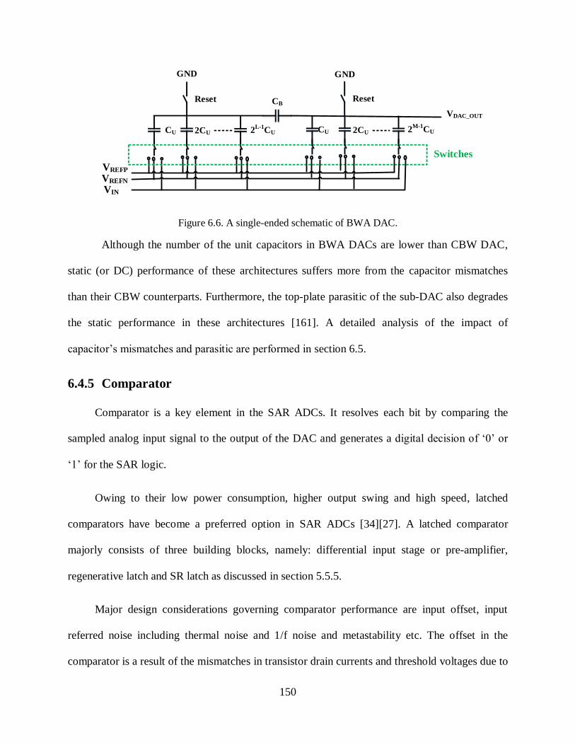
150
2CU 2L-1
CUCU
VIN
VREFN
VREFP
Switches
VDAC_OUT
CB
2CU 2M-1
CUCU
GND
Reset Reset
GND
Figure 6.6. A single-ended schematic of BWA DAC.
Although the number of the unit capacitors in BWA DACs are lower than CBW DAC,
static (or DC) performance of these architectures suffers more from the capacitor mismatches
than their CBW counterparts. Furthermore, the top-plate parasitic of the sub-DAC also degrades
the static performance in these architectures [161]. A detailed analysis of the impact of
capacitor‟s mismatches and parasitic are performed in section 6.5.
6.4.5 Comparator
Comparator is a key element in the SAR ADCs. It resolves each bit by comparing the
sampled analog input signal to the output of the DAC and generates a digital decision of „0‟ or
„1‟ for the SAR logic.
Owing to their low power consumption, higher output swing and high speed, latched
comparators have become a preferred option in SAR ADCs [34][27]. A latched comparator
majorly consists of three building blocks, namely: differential input stage or pre-amplifier,
regenerative latch and SR latch as discussed in section 5.5.5.
Major design considerations governing comparator performance are input offset, input
referred noise including thermal noise and 1/f noise and metastability etc. The offset in the
comparator is a result of the mismatches in transistor drain currents and threshold voltages due to

151
manufacturing random process variations [1]. The offset limits the minimum achievable
resolution of the comparator. It can be partially mitigated by increasing the transistor sizes and
careful layout. Metastability in the comparators occurs when the input is near the comparator
decision point and as a result the comparator is not able to generate a valid output within
designated time. One technique to reduce the probability of metastability is to increase the gain
of the pre-amplifier [147]. In addition to above, other important design considerations include
the speed, power dissipation, input capacitance and input common mode range of comparator
[147].
6.5 Background on Linearity Analysis of SAR ADCs
The targeted ADC is going to be applied in the feedback control loop of the controller of
DC/DC converter. Therefore, the ADC is required to have excellent linearity performance. In
particular, to achieve the monotonic behaviour the DNL should not exceed beyond -1 LSB.
The linearity of the overall SAR ADC is determined by the linearity of the DAC. This
section gives a detailed linearity analysis of BWA and CBW architectures for parasitic
capacitances and capacitor mismatches.
6.5.1 Effect of Parasitic Capacitance on Linearity
In order to investigate the effect of parasitic capacitances on the linearity characteristics
of capacitive-array DACs, it should be noted that the bottom-plate parasitic do not impact the
linearity as output voltage is independent of that. The top-plate parasitic capacitance to the
substrate does not impact the linearity performance of the CBW architectures but degrades the
performance of BWA architectures [161].

152
A single-ended simplified version of N-bit CBW DAC array having a unit capacitor CU
and top-plate parasitic of CPar is depicted in Figure 6.7. The binary weighted capacitors inside the
capacitor-array are controlled by the control signals which are generated from the SAR-logic.
Based on the states of control signals, voltage on the top-plate (i.e. VOUT) is given by:
ParTotal
N
0iii
REFOUT
CC
DCVV , (6.10)
Where, Ci is the ith capacitor in the DAC array, Di is the control signal from SAR logic, 2
(i-1)CU,
CTotal is the total capacitance in the array while CPar represents the parasitic capacitance
connected from the top-plate of capacitor-array to ground. It is apparent from (6.10) that CPar acts
as an attenuator that impacts the magnitude of the VOUT, but it does not influence its polarity
[161].
A single-ended version of the capacitor array in a BWA DAC is illustrated in Figure 6.8,
with MSB-side and LSB-side DACs consisting of M and L bits, respectively with M=L= N/2.
The output voltage at the top-plate of MSB-side, which connects to the comparator input, can be
written as [161]:
VREFP
GND
GNDRESET
CUCU 2CU2
N-2CU
VIN
CPar
VOUT
2N-1
CU2N-3
CU
Figure 6.7. Parasitic capacitance in CBW DAC.

153
Par_LSBTotal_LSB
1M
0iii
REFtt
Par_MSBTotal_MSB
1L
0iii
REFOUTCC
DCVCA
CC
DCVV (6.11)
Where CTotal_MSB , CPar_MSB, CTotal_LSB and CPar_LSB are the total main capacitance on MSB side of
array, parasitic capacitances on the MSB side of array, total main capacitance on LSB side of
array and parasitic capacitances on the LSB side of array, respectively while AttC is given as,
Par_LSBTotal_LSB
Utt
CC
CCA
Shown in equation (6.11), is the effect of the top-plate parasitic at the LSB-side (i.e. CPar_LSB) on
output voltage of DAC i.e. VOUT, which is not constant with changing input digital code and
hence can results in significant linearity degradation. On the other hand, the effect of top-plate
parasitic capacitances on the MSB-side (i.e. CPar_MSB) impacts the magnitude only. For the case
M=L= N/2, the maximum DNL occurs every 2N/2
code and is given as [161][167]:
U
1N
BU
2
3N
Par_LSB
N
REF
C2
CC2C2VDNL
(6.12)
Equation (6.12) shows that in order to keep the DNL within ±1 LSB, CPar_LSB should be smaller
than CU.
MSB -Side
GNDRESET
CU 2CU
VIN
CU
VOUT
2M
CU
CPar_LSB CPar_MSB
2L-1
CU2CU
CB
LSB -Side
VREFP
GND
Figure 6.8. Parasitic capacitance in BWA DAC.
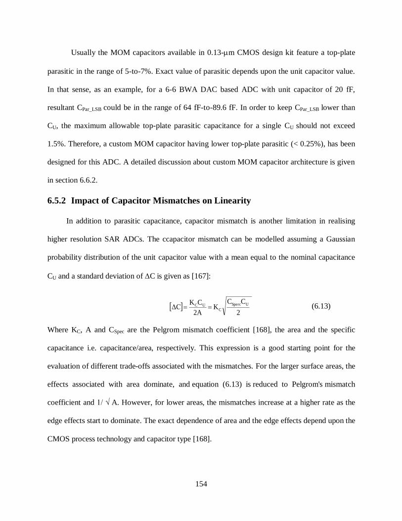
154
Usually the MOM capacitors available in 0.13-m CMOS design kit feature a top-plate
parasitic in the range of 5-to-7%. Exact value of parasitic depends upon the unit capacitor value.
In that sense, as an example, for a 6-6 BWA DAC based ADC with unit capacitor of 20 fF,
resultant CPar_LSB could be in the range of 64 fF-to-89.6 fF. In order to keep CPar_LSB lower than
CU, the maximum allowable top-plate parasitic capacitance for a single CU should not exceed
1.5%. Therefore, a custom MOM capacitor having lower top-plate parasitic (< 0.25%), has been
designed for this ADC. A detailed discussion about custom MOM capacitor architecture is given
in section 6.6.2.
6.5.2 Impact of Capacitor Mismatches on Linearity
In addition to parasitic capacitance, capacitor mismatch is another limitation in realising
higher resolution SAR ADCs. The ccapacitor mismatch can be modelled assuming a Gaussian
probability distribution of the unit capacitor value with a mean equal to the nominal capacitance
CU and a standard deviation of C is given as [167]:
2
CCK
A2
CKΔC
USperc
CUC (6.13)
Where KC, A and CSpec are the Pelgrom mismatch coefficient [168], the area and the specific
capacitance i.e. capacitance/area, respectively. This expression is a good starting point for the
evaluation of different trade-offs associated with the mismatches. For the larger surface areas, the
effects associated with area dominate, and equation (6.13) is reduced to Pelgrom's mismatch
coefficient and 1/ √ A. However, for lower areas, the mismatches increase at a higher rate as the
edge effects start to dominate. The exact dependence of area and the edge effects depend upon the
CMOS process technology and capacitor type [168].
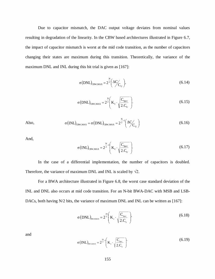
155
Due to capacitor mismatch, the DAC output voltage deviates from nominal values
resulting in degradation of the linearity. In the CBW based architectures illustrated in Figure 6.7,
the impact of capacitor mismatch is worst at the mid code transition, as the number of capacitors
changing their states are maximum during this transition. Theoretically, the variance of the
maximum DNL and INL during this bit trial is given as [167]:
U
2
N
MAXCBW, CΔC2DNL σ , (6.14)
2.C
CK2DNL σ
U
Spec
C2
N
MAXCBW,. (6.15)
Also,
U
12
N
MAXCBW,MAXCBW, CΔC2DNL σINL σ (6.16)
And,
2.C
CK2INL σ
U
Spec
C
12
N
MAXCBW,. (6.17)
In the case of a differential implementation, the number of capacitors is doubled.
Therefore, the variance of maximum DNL and INL is scaled by √2.
For a BWA architecture illustrated in Figure 6.8, the worst case standard deviation of the
INL and DNL also occurs at mid code transition. For an N-bit BWA-DAC with MSB and LSB-
DACs, both having N/2 bits, the variance of maximum DNL and INL can be written as [167]:
2.C
CK2DNL σ
U
Spec
C
4
3N
BWAMAX
, (6.18)
and
2.C
CK2INL σ
U
Spec
C
14
3N
MAXBWA,
. (6.19)

156
Random capacitor mismatch is a major source of linearity errors in SAR ADCs targeting
resolution greater than 10-bit. Due to their lower cost, MOM capacitors have become a preferred
option for the DAC implementation in SAR ADCs. Therefore, an accurate estimation of the
mismatch in the MOM capacitor is of prime importance. Table 6.2 summarises mismatch data
from two other CMOS processes. Based upon the literature and design kit data, the MOM
capacitor mismatch is approximately three times that of MIM capacitors [170]. For the current
design kit, a MIM capacitor of 16fF has a mismatch coefficient of 0.85% m. Therefore, a MOM
capacitor having the same capacitance (i.e. 16 fF), as a rough estimate, the KC can be taken as
2.55% m i.e. 3 × 0.85. For high level analysis, 3 % m is a good conservative approximation.
As discussed previously, the impact of capacitor mismatch is most pronounced at MSB-1
transition resulting in maximum INL and DNL occurring during this bit trial [27][161]. By
employing the expressions (6.18) and (6.19), with a KC of 3 %m, the value of standard variance
of the maximum DNL for a 6-6 BWA architecture is calculated for different values of CU and
CSpec. The resulting 3DNLMAX (LSB) and 3INLMAX (LSB) over a wider range of CU and CSpec
are illustrated in Figure 6.9 and Figure 6.10, respectively. These figures show that for a given CU
lower values of CSpec or higher area, results in better linearity performance. As an example, a CU
of 20 fF having a Cspec below 0.2 fF/m2 or an area of 100 m
2, can achieve the required linearity
performance (DNL < ±1LSB). In order to obtain the desired linearity performance with a higher
CSpec or smaller CU either analog or digital calibration is required.
Table 6.2. Capacitors mismatch data from different design kits.
Technology (nm)
Cap
Type Cap. Mismatch
(Std. dev %)
KC
(%m)
UMC 130 MIM 1 0.95
ST 65 MIM 5 0.5
ST 65 MOM 1 1.5
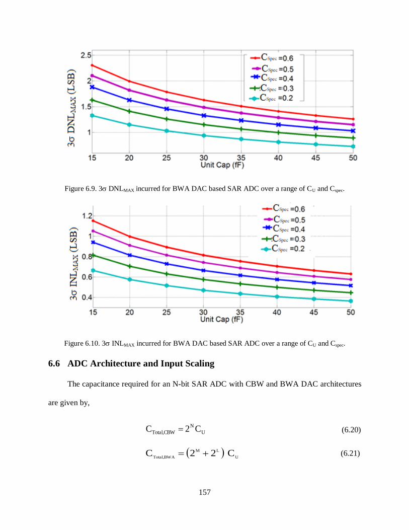
157
Figure 6.9. 3DNLMAX incurred for BWA DAC based SAR ADC over a range of CU and Cspec.
Figure 6.10. 3INLMAX incurred for BWA DAC based SAR ADC over a range of CU and Cspec.
6.6 ADC Architecture and Input Scaling
The capacitance required for an N-bit SAR ADC with CBW and BWA DAC architectures
are given by,
U
N
CBWTotal, C2C (6.20)
U
LM
BWATotal,C22C (6.21)

158
Where, M and L are the number of capacitors on MSB and LSB sides, respectively in the BWA
architecture. Although BWA architectures suffer more from the parasitic capacitances and
capacitor mismatches, the number of the unit capacitors and hence circuit complexity is much
lower [149][161]. The proposed ADC employs a 6-6 BWA architecture with bottom-plate
sampling as illustrated in Figure 6.11. This sampling technique is more favourable for
applications requiring higher linearity as the non-linearity associated with the junction capacitance
of the top-plate switch is almost zero [22] . One problem associated with the bottom-plate
sampling is that the voltage on the top of LSB-DAC could exceed the power rails i.e. 0 or 1.2 V
during the bit trials. As a result, the parasitic diode of the top-plate switches can turn ON and
cause leakage current and, hence corrupting the sampled signal.
CU 32CU16CU16CU 32CUCU
VCM
+
-VCMVCM
CB
CB
VREFN
VREFP
CU16CU16CU 32CUCU
VCM
VREFN
VREFP
3.3 V Switches
3.3 V Switches
32CU
A
B
X
Y
(8x4CU)
(8x4CU)(4x4CU)
(4x4CU)(8x4CU)
(8x4CU)(4x4CU)
(4x4CU)
VIN_N
VIN_P
Chop Control
Figure 6.11. Proposed 6-6 BWA 12-bit SAR ADC architecture with input scaling.

159
In this architecture, input sampling scaling is realised by only sampling the input signal
onto the bottom plates of the MSB and MSB-1 capacitors while the common mode voltage
(VCM) is sampled onto the bottom-plate of all the remaining capacitors as shown in Figure 6.12.
This has the effect of scaling the input signal by a factor of three quarters of the initial input
voltage. By employing a different number of input capacitors during sampling phase, this
technique can be further extended to realise different input scaling ratios to enable larger input
ranges.
6.6.1 Switches
NMOS are used to connect the capacitors of the DAC to the reference voltages (VREFP
and VREFN), the input signal (VIN) and the common mode voltage (VCM). In order to balance the
parasitic capacitance and to facilitate the capacitor segmentation, a modular design approach has
been used when designing and completing the capacitor array.
The capacitors in the DAC are arranged in the columns of 4 unit capacitors (i.e. CUs). An
equivalent single-ended DAC schematic is shown in Figure 6.13.
CU 32CU16CU16CU 32CUCU
VCM
VCMVCMCB
(8x4CU)(4x4CU)(8x4CU)(4x4CU)
VIN_N
Figure 6.12. Sampling of the input voltage.
VCM
VREFN
VREFP
4CU4CU4CU 4CU 4CU
VCM
SWREFP SWREFN
SWIN
SWCM
SWS-H
32CU
4CU
16CU
VCM
4CU
MSB and MSB -1 capacitors
consisting of 12 columnsCB
VIN
Figure 6.13. Simplified schematic of SE DAC of the SAR ADC.

160
Hence, the MSB capacitor consists of 8 columns; the MSB-1 capacitor consists of 4 columns
and so on. Each capacitor column is controlled by an independent set of three switches (SWREFP,
SWREFN and SWIN.). The top plates of all the columns either MSB-DAC or LSB-DAC are
shorted together and connected to VCM using the SWCM switch. The reference switches (SWREFP
and SWREFN) are activated during various bit trials to connect the bottom plates of the capacitors
to VREFP and VREFN, respectively.
The ADC employs 3.3 V NMOS IO devices for the input (VIN, 0-to-3.2 Vpp_d), VREFP (1.2 V),
VREFN (0 V) and VCM (0.8 V) switches.
6.6.2 Custom MOM Capacitors
As discussed in section 6.5.1, in terms of parasitic, a DNL of ±1 LSB requires the capacitors
with a top-plate parasitic less than 1.5 %. Therefore, a custom MOM capacitor having top-plate
parasitic lower than 0.25 % has been designed. The top and cross-sectional views of the designed
custom MOM capacitor are depicted in Figure 6.14 (a) and (b), respectively.
B
(a)
B BT B T B B TT
(b)
B=Bottom PlateT=Top Plate
BT
B
Figure 6.14. MOM Capacitor (a) Top view (b) Cross-sectional view.
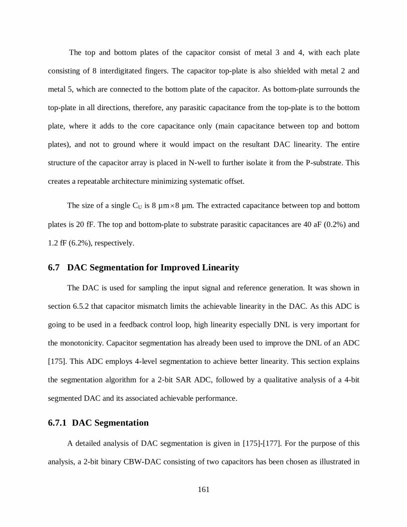
161
The top and bottom plates of the capacitor consist of metal 3 and 4, with each plate
consisting of 8 interdigitated fingers. The capacitor top-plate is also shielded with metal 2 and
metal 5, which are connected to the bottom plate of the capacitor. As bottom-plate surrounds the
top-plate in all directions, therefore, any parasitic capacitance from the top-plate is to the bottom
plate, where it adds to the core capacitance only (main capacitance between top and bottom
plates), and not to ground where it would impact on the resultant DAC linearity. The entire
structure of the capacitor array is placed in N-well to further isolate it from the P-substrate. This
creates a repeatable architecture minimizing systematic offset.
The size of a single CU is 8 µm8 µm. The extracted capacitance between top and bottom
plates is 20 fF. The top and bottom-plate to substrate parasitic capacitances are 40 aF (0.2%) and
1.2 fF (6.2%), respectively.
6.7 DAC Segmentation for Improved Linearity
The DAC is used for sampling the input signal and reference generation. It was shown in
section 6.5.2 that capacitor mismatch limits the achievable linearity in the DAC. As this ADC is
going to be used in a feedback control loop, high linearity especially DNL is very important for
the monotonicity. Capacitor segmentation has already been used to improve the DNL of an ADC
[175]. This ADC employs 4-level segmentation to achieve better linearity. This section explains
the segmentation algorithm for a 2-bit SAR ADC, followed by a qualitative analysis of a 4-bit
segmented DAC and its associated achievable performance.
6.7.1 DAC Segmentation
A detailed analysis of DAC segmentation is given in [175]-[177]. For the purpose of this
analysis, a 2-bit binary CBW-DAC consisting of two capacitors has been chosen as illustrated in

162
Figure 6.15. Here CU1 represents the LSB-capacitor while the MSB-capacitor is split into two
equal parts; CU2,0 and CU2,1. All of these unit capacitors have equal capacitances i.e. CU2,1= CU2,0=
CU1= CU. Figure 6.15 (a) and (b) shows the switching of the capacitor array in conventional and
segmented DACs, respectively.
The conversion process starts by sampling the input signal onto the bottom plates of all
capacitors. During the sampling phase, the connections of all the capacitors are the same in both
types of DAC i.e. conventional and segmented DACs. After sampling the input signal, during the
first bit trial, all MSB capacitors (i.e. CU2,0 and CU2,1) are connected to VREFP i.e. positive
reference, while the LSB-capacitor CU1 is connected to VREFN i.e. negative reference.
(a)
(b)(b)
Figure 6.15. 2-bit SAR ADC operation with (a) Normal DAC (b) Segmentation DAC.
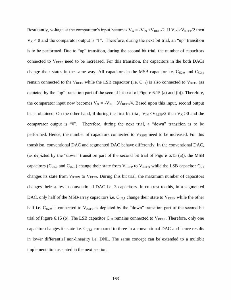
163
Resultantly, voltage at the comparator‟s input becomes VX = -VIN +VREFP/2. If VIN >VREFP/2 then
VX < 0 and the comparator output is “1”. Therefore, during the next bit trial, an “up” transition
is to be performed. Due to “up” transition, during the second bit trial, the number of capacitors
connected to VREFP need to be increased. For this transition, the capacitors in the both DACs
change their states in the same way. All capacitors in the MSB-capacitor i.e. CU2,0 and CU2,1
remain connected to the VREFP while the LSB capacitor (i.e. CU1) is also connected to VREFP (as
depicted by the “up” transition part of the second bit trial of Figure 6.15 (a) and (b)). Therefore,
the comparator input now becomes VX = -VIN +3VREFP/4. Based upon this input, second output
bit is obtained. On the other hand, if during the first bit trial, VIN <VREFP/2 then VX >0 and the
comparator output is “0”. Therefore, during the next trial, a “down” transition is to be
performed. Hence, the number of capacitors connected to VREFN need to be increased. For this
transition, conventional DAC and segmented DAC behave differently. In the conventional DAC,
(as depicted by the “down” transition part of the second bit trial of Figure 6.15 (a)), the MSB
capacitors (CU2,0 and CU2,1) change their state from VREFP to VREFN while the LSB capacitor CU1
changes its state from VREFN to VREFP. During this bit trial, the maximum number of capacitors
changes their states in conventional DAC i.e. 3 capacitors. In contrast to this, in a segmented
DAC, only half of the MSB-array capacitors i.e. CU2,1 change their state to VREFN while the other
half i.e. CU2,0 is connected to VREFP as depicted by the “down” transition part of the second bit
trial of Figure 6.15 (b). The LSB capacitor CU1 remains connected to VREFN. Therefore, only one
capacitor changes its state i.e. CU2,1 compared to three in a conventional DAC and hence results
in lower differential non-linearity i.e. DNL. The same concept can be extended to a multibit
implementation as stated in the next section.

164
6.7.2 Linearity Analysis of Segmented DAC Array
DAC segmentation can significantly improve the resultant DNL. This can be explained
with an example from [175]. A BWA DAC having M and L number of bits in the MSB and
LSB-DACs, respectively, is shown in Figure 6.16. In this architecture, the capacitance seen from
node B towards the left, can be represented as CS and can be written as:
U
UU
L
2
U
L
S CCC)12(
C)12(C
. (6.22)
The maximum error due to capacitor mismatch occurs at the (MSB-1)th
bit transition as
the maximum number of capacitors change their state during this bit trial. In order to calculate
the error due to capacitor mismatch, we assume VX as the voltage at top-plate of the MSB-DAC
during MSB-trial and VX’ is the voltage after the transition i.e. during (MSB-1)
th trial.
During the MSB-bit trial, the MSB capacitor i.e. 2M-1
CU in the MSB-DAC are connected
to VREFN, while all the remaining capacitors in the MSB-DAC i.e. CU-to-2M-2
CU and all the
capacitors in LSB-DAC i.e. CU-to-2L-1
CU are connected to the VREFP as shown in Figure 6.17 (a).
(Same analysis can be carried out for the opposite case i.e. MSB capacitor in the MSB-DAC
being connected to VREFP and remaining capacitors to VREFN.)
2M-1
CUCU
CBVX
2M-2
CU2CU
MSB-DAC
2L-1
CUCU 2L-2
CU2CU
LSB-DAC
CU
B]CS
Figure 6.16. BWA DAC consisting of M and L numbers of bits in the MSB and LSB-DACs.

165
The voltage at the top-plate on the MSB-DAC is given by:
Total_LSB
1M
0iii
REFP
Total_LSB
U
Total_MSB
1L
0iii
REFPX
C
DCV
C
C
C
DCVV
. (6.23)
During the MSB-bit trial,
REFP
U
NM
U
1M
XV
)C2(12
1)C-(2V
(6.24)
REFP
U
M
U
1M
XV
C2
1)C-(2V
(6.25)
Now consider the MSB-1 bit trial as shown in Figure 6.17 (b). All of the unit capacitors in the
MSB capacitor are connected to VREFP while all the remaining capacitors switch their state to
VREFN , as shown in Figure 6.17 (b).
2M-1
CUCU
CBVX
2M-2
CU2CU
MSB-DAC
2L-1
CUCU 2L-2
CU2CU
LSB-DAC
CU
B]CS
1000
0000
0
2M-1
CUCU
CBVX
,
2M-2
CU2CU
MSB-DAC
2L-1
CUCU 2L-2
CU2CU
LSB-DAC
CU
B]CS
011111 111
MSB Bit Trial
MSB-1 Bit Trial
(a)
(b)
Figure 6.17. Capacitor states during (a) MSB-bit trial (b) MSB-1 bit trial.

166
The voltage at the top-plate VX’ is now given by:
.VC2
C2V
)C2(12
C2V
REFP
U
M
U
1M
REFP
U
NM
U
1M
,
X
(6.26)
Ideally, the difference of VX to VX’ equals to VREFP/2
M. It can be written as follows:
M
REFPREFP
U
M
1M1M
U
1M,
XX2
VV
C2
1)2(2C2VV
(6.27)
If the standard deviation for the capacitor mismatch in CU is ΔCU, the real value of the unit-
capacitor C can be written as:
UU CC C . (6.28)
Therefore, equitation (6.27) can be written as:
REFPM
1M1M1M
,
XXV
C2
1)2(2C2VV
. (6.29)
All unit capacitors are connected in parallel with each other in the DAC. If the total number of
capacitors connected in parallel is N, the standard deviation of the total capacitance in the
capacitor array is √N ΔCU. Therefore, the standard deviation of VX - VX’ can be calculated as:
,VC2C2
ΔC121)C(2ΔC2C2)VV σ(
REFP
U
M
U
M
U
1M
U
1M
U
1M
U
1M
,
XX
(6.30)
REFP
U
M
U
1M
U
1M
U,
XX VC2
ΔC12ΔC2C)VV (
. (6.31)
Therefore, the variance of maximum DNL incurred during this code transition is given by:
Ideal
,
XXstd
,
XXNormalMaximum, )VV ()VV (DNLσ ,
(6.32)
REFP
U
U
M
1M
NormalMaximum, VC
ΔC
2
2DNLσ
.
(6.33)

167
Now consider the DAC where upper “K” bits out of the “M” bits are segmented as
illustrated in Figure 6.18. Here the upper “K” bits of MSB-DAC are rearranged in multiple
columns to ease the segmentation. In this configuration, the maximum number of switching
occurs during the bit trial when all the capacitors in the (M-K)th binary weighted capacitors
change their state from VREFN to VREFP. The capacitor array before and after the code transition is
shown in Figure 6.19 (a) and (b), respectively.
2M-K
CUCU
CB VX
2M-K
CU2CU
MSB-DAC
LSB-DAC ]CS
2M-K
CU
Upper K bits segmented M-K bits binary weighted
Figure 6.18. Segmented MSB-DAC where upper K bits in MSB-DAC are segmented.
2M
CUCU
CBVX
2M-K+1
CU2CU
LSB-DAC
2M-K
CU
M-K bits binary weighted
2M-K-1
CU
1 01 1 0 0
2M
CUCU
CBVX
2M-K+1
CU2CU
LSB-DAC ] 2M-K
CU
M-K bits binary weighted
2M-K-1
CU
0 10 0 0 0
]1 01 1 0 0
0 10 0 0 0
Code transition
(a)
(b)
K segmented bits
K segmented bits
Figure 6.19. Code transition where maximum number of capacitors in segmentation DAC change their
state (a) Before transition (b) After transition.

168
The maximum DNL and INL occur during this bit trial. The voltage at the top-plate of the
MSB-DAC before and after the code transition as depicted in Figure 6.19(a) and (b) i.e. VX and
VX‟are given by (6.34) and (6.35), respectively:
REFPM
KM
X VC2
1)C(2V
, (6.34)
RREFPM
KM
,
X VC2
C2V
, (6.35)
Using the same procedure as explained before, the variance of maximum DNL can now be written
as follows:
,)VV ()VV (DNLσIdeal
,
XXstd
,
XXSegmentedMaximum, (6.36)
REFP
U
M
U
KM
U
KM
SegmentedMaximum, VC2
ΔC12ΔC2DNLσ
. (6.37)
Which simplifies to:
RREFP
U
U
M
1KM
SegmentedMaximum, VC
ΔC
2
12DNLσ
(6.38)
Comparison of equations (6.33) and (6.38) shows that the maximum standard deviation
of the DNL in the segmented DAC is reduced by a factor of √2K-1
.
In the proposed architecture, the upper 4 bits of the MSB-DAC are segmented. 4-bit
segmentation ideally reduces the variance of maximum DNL by a factor of √8 (or 2.82). In order
to facilitate this segmentation, the capacitors in the DAC are arranged in columns where each
column consists of 4 CUs as depicted Figure 6.20, with two dummy rows above and below. Each
of these columns is controlled by an independent set of 3 switches i.e. VIN, VREFP and VREFN,
which are driven by the control signals generated by SAR logic. For 4-level capacitor
segmentation, 17 additional signals are generated from the SAR logic. In order to validate the

169
capacitor segmentation algorithm, a set of Monte Carlo runs with Gaussian distributed mismatch
errors CU /CU=0.5-to-3% were performed at the behavioural level of the circuit, that validated
the DNL improvement. As an example, Figure 6.21 shows the DNL plot of the 12-bit SAR ADC
with conventional and segmented DACs while having 0.81 % mismatch in the MSB and the
MSB-1 capacitors.
Figure 6.20. Layout of 12-bit DAC to facilitate the segmentation.
Figure 6.21. DNL plots of 12 SAR ADC, 0.81% mismatch in MSB and MSB-1 in 6-6 BWA based SAR
ADC with conventional and segmented DACs.

170
6.8 Comparator
The designed 12-bit SAR ADC employs a double tail latch comparator as shown in Figure
6.22 [178]. This architecture is more suited to lower-supply voltages as the number of stacked
transistors are lower compared to a conventional dynamic comparator. These comparators do not
dissipate any static power. Furthermore, these comparators allow larger currents in the latching
stage for higher speed while maintaining lower current in the input stage for lower offset.
During the reset phase i.e. CLK = 0, the transistors M4 and M5 charge the two nodes “P”
and “N” to supply voltage, VDD. As a result, transistors M9 and M10 turn ON and discharge the
output nodes, OUT-P and OUT-N, to ground. During the ON phase, CLK =VDD, the transistors
M4 and M5 turn off and an input-dependent differential voltage ΔVPN is formed between the
nodes, “P” and “N”. This voltage is then transferred to the regenerative latch, consisting of M6,
M7, M8 and M9, which generates the outputs, OUT-P and OUT-N, that are then passed to the
SR-Latch. Table 6.3 and Table 6.4 present the transistor sizes and the simulation results of the
comparator, respectively.
VDD
OUT-POUT-N
IN-P IN-N
CLK
N
M2 M3
M4 M5
M6 M7
M8 M9
M12
M13
M14
M9 M10
P
M1
Figure 6.22. Double-tail latch comparator.

171
Table 6.3. Transistor sizes in double tail latch comparator.
Devices Type Size(m) M1 NMOS 4/0.26
M2, M3 NMOS 24/0.26
M4, M5 PMOS 4/0.26
M6, M7 NMOS 8/0.26
M8, M9 PMOS 24/0.26
M10, M11 NMOS 16/0.26
M12 PMOS 4/0.26
Table 6.4. Simulation results of comparator.
Specification Value Offset (std. dev, mV) 1.59
RMS Noise (V) 88
Current (A) 90
6.8.1 Comparator Offset Removal
The comparator offset can vary with time due to temperature and aging effects and is the
primary source of offset within the ADC. The proposed ADC is going to be incorporated in a
system that will have a life span of several years (5-to-10) and hence requires an accurate and
dynamic estimation of the ADC offset during its lifespan. A chopping circuit is placed at the
comparator‟s differential inputs shown in Figure 6.23. The SAR ADC operation sequence for the
ADC during the offset-calculation mode is depicted in Figure 6.24. As a first step, the nodes A
and B are initially connected to nodes X and Y, respectively as shown in Figure 6.23. After the
reset and sampling phase, the SAR algorithm goes through a regular bit-trial sequence. However,
instead of progressing to the next sample, the comparator inputs are then switched, thus
connecting nodes A and B with Y and X, respectively and a second sequence of bit trials is
performed. The two respective digital outputs are then processed to determine the offset.

172
CU 32CU16CU16CU 32CUCU
VCM
+
-VCMVCM
CB
CB
VREFN
VREFP
CU16CU16CU 32CUCU
VCM
VREFN
VREFP
3.3 V Switches
3.3 V Switches
32CU
A
B
X
Y
(8x4CU)
(8x4CU)(4x4CU)
(4x4CU)(8x4CU)
(8x4CU)(4x4CU)
(4x4CU)
VIN_N
VIN_P
Chop Control
Figure 6.23. Full schematic of ADC with chopping in front of comparator.
SAR logic
12 bit trial
SAR logic
12 trial
Reset
Sample
Chopp
Bit trials with
point A to X and point B to Y
Time
SAR
Bit trials with
point A to Y and point B to X
1 2 3 272625244
Figure 6.24. ADC operation sequence in offset-calculation.
The offset-calculation can be performed for any input level. When run in offset-calculation
mode, the two output codes obtained are subsequently averaged and the comparator offset is
determined. Based upon the requirement of offset-calculation frequency, the ADC can be run in
this mode. The ADC has a conversion time of 0.5 s when the output rate = 2 MS/s and requires
1 s in offset-calculation mode. As an example, the ADC can be run in normal mode for a longer
time (let‟s say 1 ms) and then in the offset-calculation mode for a single time (i.e. 1s). In this
sense, the impact of offset-calculation upon the throughput of ADC is not significant. Offset-

173
calculation mode is activated using a control signal of SAR logic that can be controlled from
outside. The offset calculation mode can also be used to reduce the comparator‟s 1/f noise.
6.9 ADC Layout
The 12-bit SAR ADC is fabricated in a 0.13-m 1P6M CMOS process. For better noise
isolation, all NMOS devices are placed in a deep-n-well (DNW). The following subsections
briefly explain the layout of the different circuit blocks.
6.9.1 DAC
The unit capacitors in the DAC are arranged in columns with each column consisting of 4
CUs, with additional dummy capacitors added for matching purposes. All the capacitor columns
in the array are arranged in pseudo common centroid fashion to facilitate the routing and at the
same time improve the relative matching as depicted in Figure 6.25. Here 32, 16, 8 represent
MSB, MSB-1 and MSB-2 capacitors, respectively and so on. The complete capacitor array is
surrounded by two rows, above and below, and two columns at either ends of dummy capacitors.
It was stated in section 6.6.1 that the switches employed in DAC are 3.3 V NMOS while the
SAR logic employs 1.2 V devices. Therefore, level shifters are required between SAR logic and
DAC switches. Moreover, to make the complementary references (VREFP, VREFN) going to single
capacitor columns non-overlapping, a break-before-make (BBM) circuit has been employed.
Each capacitor column is controlled by a single set of switches along with corresponding level
shifters and BBM. The arrangement of capacitor array column, BBM, level shifter and SAR
logic is shown in Figure 6.26. A complete layout of the DAC is shown in Figure 6.27.
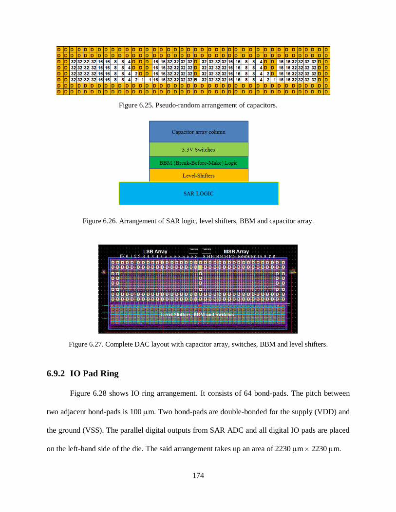
174
Figure 6.25. Pseudo-random arrangement of capacitors.
Figure 6.26. Arrangement of SAR logic, level shifters, BBM and capacitor array.
Figure 6.27. Complete DAC layout with capacitor array, switches, BBM and level shifters.
6.9.2 IO Pad Ring
Figure 6.28 shows IO ring arrangement. It consists of 64 bond-pads. The pitch between
two adjacent bond-pads is 100 m. Two bond-pads are double-bonded for the supply (VDD) and
the ground (VSS). The parallel digital outputs from SAR ADC and all digital IO pads are placed
on the left-hand side of the die. The said arrangement takes up an area of 2230 m 2230 m.

175
Figure 6.28. IO ring layout.
6.9.3 Full Chip Layout
The ADC layout along with the IO ring is shown in Figure 6.29. The dimensions of the
core ADC are 640 m 370 m. The vacant regions of the chip are filled with decoupling
capacitors to provide on-chip decoupling for the supplies, references and VCM. A detailed
version of the core ADC layout with individual blocks is shown in Figure 6.30.

176
Core ADC
Figure 6.29. Core ADC and IO ring.
SAR Logic
BBM
Level Shifters
Bottom Plate Switches
Cap. Array
Comparator and Chopping
Circuit
Figure 6.30. Core ADC sub-blocks.

177
6.10 Experimental Characterization
The chip micrograph of ADC is shown in Figure 6.31 which shows the SAR logic, level
shifters, switches and capacitor array.
Figure 6.31. Chip micrograph and core ADC.
178
6.10.1 Test PCB
The test PCB schematic is shown in Figure 6.32 and a photograph of the resultant PCB is
shown in Figure 6.33. In order to make the PCB debugging and operation easier, a simple
schematic was employed for the test PCB. The following considerations highlight some of the
test PCB aspects:
1. To minimise the bond-wire inductance caused due to lengthy bond wires of the package,
the chip is directly wire bonded on the PCB.
2. The differential input signal is provided to the design-under-test (DUT) from an external
signal generator. No AAFs were placed on the PCB. Filtering and common-mode of the
differential signal can be generated from an external board e.g. breadboard.
3. All the power supply voltages (3.3 V, 1.2 V, 0 V,) common mode voltage (0.8 V), along
with reference voltages (1.2 V and 0 V) are supplied externally without using any
regulator on the PCB. Each of the supplies has a dedicated connector on the PCB. This
results in more area consumption on the PCB but provides flexibility and ease of control.
Anti-aliasing filtering of the input signal is provided using external capacitors and
resistors.
4. Decoupling capacitors have been extensively used between all the power supplies,
common mode, references (1.2 V) and grounds.
5. The PCB has 4 layers with separate ground and power planes.

179
D0
D1
D2
D3
D4
D5
GG
ND
DV
DD
GG
ND
3V
3
GV
DD
3V
3
D6
D7
D8
D9
D1
0
D11
GGND3V3
GGND
GGND1V2
vss_dac
vss_dac
vdd_dac
vdd_dac
vrefn_dac
vrefp_dac
vddc_comp
vss_latch
vdd_latch
GGND
GVDD1V2
vrefp
_0p
8V
_buff
PD
_refb
PD
_buff
I_ref-b
uff
vin
n_ex
t_buff
Vin
put_
buff
vss_
reff_buff
vss_
sub
vdda_
buff
vssa
_buff
DG
ND
I_ref_
refb
vgg_refb
vdd
_refb
vin
p_ex
t_buff
vss_
refb
GGND3V3
GGND
GVDD1V2
en_comp_out
en_clk_out
chop_mode
soc_flag
reset
comp_out
GGND3V3
eoc_flag
chop_mode_flag
CLK
CLK_out
GGND3V3
GVDD3V3
C9
100 n
F
C10
10
J3J4
J2
C9
100 n
F
C1
0
10
J5
J7J8
X2
X3
X4
J9
J11
GV
DD
3V
3
DG
ND
DG
ND
P6
P7
C19
100 nF
C20
10
C21
100 nF
C22
10
J15
C23
100 nF
C24
10
J16
vcm_dac
vddc_latch
J14
C29
100 n
F
C30
10
C25
100 n
F
C26
10
C27
100 n
FC
28
10
J13
C19
100 n
F
C20
10
C19
100 n
F
C20
10
J9
DV
DD
1V
2DG
ND
1V
2D
GN
D1V
2
C19
100 n
F
C20
10
J10
GV
DD
3V
3DG
ND
1V
2D
GN
D1V
2
DG
ND
1V
2
DG
ND
1V
2
DV
DD
1V
2
TP
11
TP
10
TP
9T
P8
TP
7T
P6
TP
0T
P1
TP
2T
P3
TP
4T
P5
GV
DD
3V
3
DG
ND
P5
GV
DD
3V
3
DG
ND
P4
GV
DD
3V
3
DG
ND
P3
GV
DD
3V
3
DG
ND
P2
GV
DD
3V
3DG
ND
P1
GV
DD
3V
3
C19
100 n
FC
20
10
GV
DD
3V
3
DG
ND
C19
100 n
F
C20
10
GV
DD
3V
3
DG
ND
C19
100 n
F
C20
10
GV
DD
1V
2
DG
ND
X1
CL
K_O
UT
CH
OP
_M
OD
E_
FL
AG
_O
UT
EO
C_F
LA
G
D10
D11
D8
D9
D7
D6
D4
D5
D1
D2
D3
D0
Lo
gic
An
aly
ser
Co
nn
ecto
r
CH
OP
_M
OD
E_FL
AG
_O
UT
EO
C_FL
AG
CL
K_O
UT
Dec
ou
plin
g
Cap
acito
rs
Hig
h S
peed
Co
nn
ecto
rs
Con
nec
tors fo
r Pow
er S
up
plie
s
an
d R
eferen
ces
Figure 6.32. Test PCB schematic

180
DUT
Figure 6.33. Photograph of the test-PCB with a close up of DUT
6.10.2 Test Setup
A block diagram of test setup is shown in Figure 6.34. A differential input or sinusoid
signal is provided using an arbitrary function generator (Tektronix 3022C). A highly precise DC
voltage source capable of providing the voltages with nV accuracy (Keithley 2602A) has been
utilised for the reference and common mode voltage generation. The master clock is generated
by an Agilent 33250A signal source. The digital output bit streams are captured by the
oscilloscope (MSO 4104). A Labview®
project on the workstation controls all the equipment and
stores the data which is later processed in Matlab®.
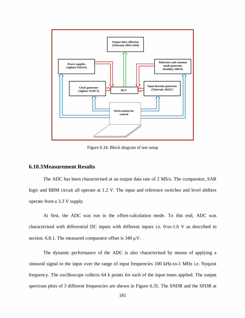
181
DUT
Input function generator
(Tektronic 3022C)
Reference and common
mode generator
(Keithley 2602A)
Power supplies
(Agilent E3631A)
Clock generator
(Agilent 33250 A)
Work station for
control
Output data collection
(Tektronic MSO 4104)
Figure 6.34. Block diagram of test setup
6.10.3 Measurement Results
The ADC has been characterised at an output data rate of 2 MS/s. The comparator, SAR
logic and BBM circuit all operate at 1.2 V. The input and reference switches and level shifters
operate from a 3.3 V supply.
At first, the ADC was run in the offset-calculation mode. To this end, ADC was
characterised with differential DC inputs with different inputs i.e. 0-to-1.6 V as described in
section. 6.8.1. The measured comparator offset is 340 V.
The dynamic performance of the ADC is also characterised by means of applying a
sinusoid signal to the input over the range of input frequencies 100 kHz-to-1 MHz i.e. Nyquist
frequency. The oscilloscope collects 64 k points for each of the input tones applied. The output
spectrum plots of 3 different frequencies are shown in Figure 6.35. The SNDR and the SFDR at
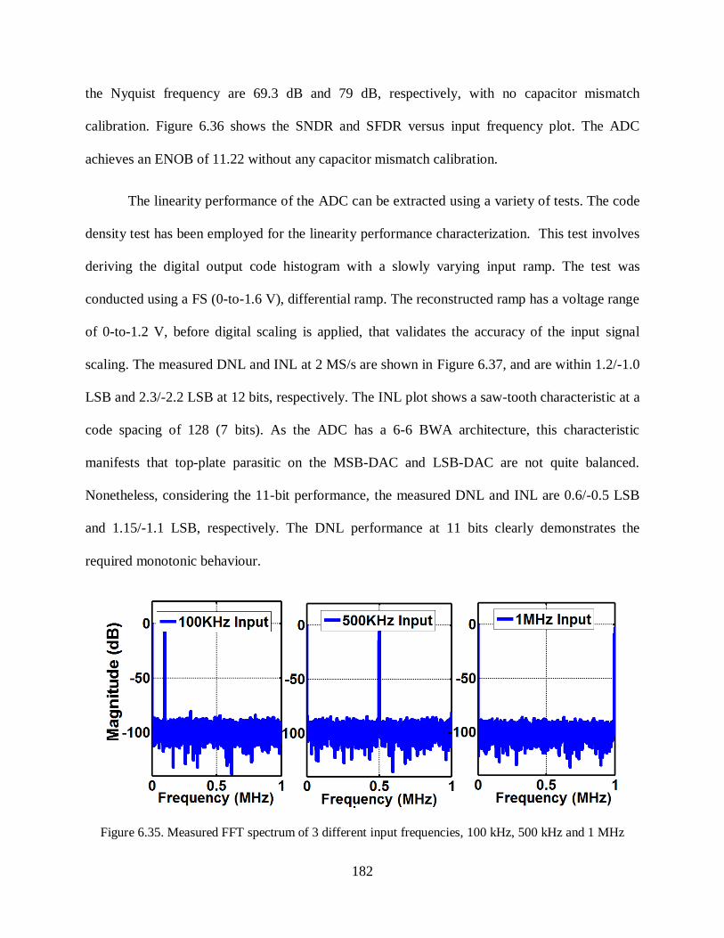
182
the Nyquist frequency are 69.3 dB and 79 dB, respectively, with no capacitor mismatch
calibration. Figure 6.36 shows the SNDR and SFDR versus input frequency plot. The ADC
achieves an ENOB of 11.22 without any capacitor mismatch calibration.
The linearity performance of the ADC can be extracted using a variety of tests. The code
density test has been employed for the linearity performance characterization. This test involves
deriving the digital output code histogram with a slowly varying input ramp. The test was
conducted using a FS (0-to-1.6 V), differential ramp. The reconstructed ramp has a voltage range
of 0-to-1.2 V, before digital scaling is applied, that validates the accuracy of the input signal
scaling. The measured DNL and INL at 2 MS/s are shown in Figure 6.37, and are within 1.2/-1.0
LSB and 2.3/-2.2 LSB at 12 bits, respectively. The INL plot shows a saw-tooth characteristic at a
code spacing of 128 (7 bits). As the ADC has a 6-6 BWA architecture, this characteristic
manifests that top-plate parasitic on the MSB-DAC and LSB-DAC are not quite balanced.
Nonetheless, considering the 11-bit performance, the measured DNL and INL are 0.6/-0.5 LSB
and 1.15/-1.1 LSB, respectively. The DNL performance at 11 bits clearly demonstrates the
required monotonic behaviour.
Figure 6.35. Measured FFT spectrum of 3 different input frequencies, 100 kHz, 500 kHz and 1 MHz

183
Figure 6.36. SNDR and SFDR vs. input frequency
Figure 6.37. Measured INL and DNL at 2MS/s
The prototype consumes a total power of 0.82 mW. The comparator and the BBM circuit
consume 0.13 mW, while the SAR logic takes 0.23 mW, all operating from a 1.2 V supply. The
level shifters consume an additional 0.46 mW. Table 6.5 summarises the measured performance
of the ADC. A comparison of the measured results with different state-of-art designs is presented
in Table 6.6.

184
Table 6.5. Measured performance of SAR ADC
Process 0.13 m
Active Area (mm2) 0.24 (0.35 mm X 0.657 mm)
Supply Voltage 1.2/3
fS (MHz) 2
Peak SFDR (dB) at 1 MHz 79
Peak SNDR (dB) at 1 MHz 69.3
Comparator Offset (LSB) < 0.5
Power Consumption (mW)
Comparator and BBM 0.13
SAR Logic 0.23
Level Shifters 0.46
Table 6.6. Comparison of the measured performance with different state of the art designs
a Sampling Rate is 2 MS/s with an oversampling ratio of 8.
b Extrapolated to 12 bits c Without level shifters
Specification Technology
(m)
Supply Voltage VDD,
(V)
Data Rate
(MS/s)
Input Signal
Swing( V )
DNL (LSB)
INL (LSB)
Resolution ENOB Power (mW)
FoMW (fJ/conv.step)
FoMS (dB)
[148] 0.18 1 0.1 1 (VREF)
b. ±2 .4
b ±2.8 12 9.4 0.0038 56 159.53
[179] 0.13 1.2 50 2 (±VREF)
0.91/-0.63
1.27/ -1.36
10 9.18 0.82 29
161.86
[180] 0.13 1 11 ±0.8 ±3.0 12 10.1 3.57 311 154.43
[182] 0.065 0.7 1.00E-03
0.7 (VREF)
0.48/ -0.55
0.52/ -0.61
10 9.1 3.00E-06
5.5
161.86
[183] 0.04 0.45 0.2 0.9 0.44 0.45 10 8.95 8.40E-
05
0.85
154.43
[184] 0.18 0.45 0.2 0.9 <0.5 <1 9 8.27 9.40E-04
22
159.53
[185] 0.04 1 6.4 1.08/-
1
3.79 13 10.35 0.046 5.5
168.76
[186] 0.065 1.2 50 2.4 (±VREF) 0.5/-
0.7
1.0/-
0.9
12 10.9 2.09 21.9
176.39
[187] 0.13 1.2 a.
0.25 10 12 0.061 59.5 161.81
[188] 0.35 3.3 0.25 50 0.55 1.81 14 13.03 4.29 2050 172.49
[189] 0.18 0.75 0.01 0.75 0.6/-
0.37
0.94/-
0.89
11 9.76 250E-6 28.8
168.15
[190] 0.065 1.2 1.25 0.74/-
0.53
0.74/-
0.80
12 11.25 44.1E-3 14.4
167.11
[191] 0.18 1.8 1.07 0.6/-
0.6
1.2/-
1.2
10 8.8 63.6E-3 130.8
154.8
This Work 0.13 1.2/3.3 2 3.2 (±1.33VREF)
1.2/-
1.0
2.3/-
2.2
12 11.22 0.9 c.
0.44 189 c. 93
159.76 c. 162.86

185
One of the salient features of the proposed ADC compared to the similar architectures
designed in the same process nodes, ([179] and [180]), is the embedded input scaling. The chip is
can digitize an extended input range of 3.2 Vpp-d, compared to 2 Vpp-d and 2.4 Vpp-d in previous
publications art i.e. [179] and [186] which corresponds to ±1.33 times the reference voltage. By
employing the reduced number of capacitors during the sampling phase, other different scaling
factors can be easily achieved. This makes it an attractive option for the sensor-based systems.
The designed ADC has also shown comparable performance in terms of linearity. The
architecture reported in [185] achieves a DNL of 1.08/-1 LSB and INL of 3.79 LSB but at the
cost of background calibration for capacitor mismatch and comparator offset. Similarly, the
architecture reported in [186] also used a background calibration for capacitor mismatch. The
designed ADC does not require any capacitor calibration and can achieve a monotonic behaviour
at 11-bits. Other competitive SAR ADCs are the ones reported in [187] and [188]. The former
includes noise-shaping while the later uses a higher supply voltage. [190] and [191] are two
other recent examples of SAR ADCs. The architecture reported in [190] is a 12-bit 8-4 BWA
DAC neural-network-based SAR ADC. [191] is also a Secure SAR ADC architecture.
Overall, it can be concluded that the input scaling technique presented in this design can be
easily embedded in a SAR ADCs, while achieving a performance competitive with the state of
the art. The presented chip does not achieve the lowest FoM, although that was not the main
design goal of this design. Instead, the main design objective and an attractive feature of the
ADC circuit is the offset calculation mechanism. This technique enables a dynamic control of
offset calculation over the whole operational life of the chip. All these features, together with the
measured performance metrics, make the proposed ADC a suitable option for integration in a
digital controller of DC/DC converters.

186
6.11 Conclusion
This chapter described the details of a 12-bit SAR ADC for a digital controller in a DC/DC
converter. Starting from the brief introduction of PMICs, a detailed analysis of ADCs for DC/DC
converters was presented. Based upon the architectural level exploration of the different ADC
architectures, a SAR ADC was selected for the target application. Finally, the circuit level
design, layout and experimental characterisation of the proposed 12-bit SAR ADC capable of
digitizing an extended input range of 3.2 Vpp-d which is ±1.33 times the reference voltage, having
improved linearity and offset correction, was presented.

187
Chapter 7: Conclusions and Future Work
7.1 Conclusions
The research work carried out in this thesis has focused on the design of high-performance
ADCs considering two different architectures which dominate the current state of the art: Ms
and SAR. Ms can achieve higher resolution while the SAR ADCs are better suited for the
low power applications with low to medium resolution.
In that scenario, the thesis has discussed the architectural level exploration, circuit level
design, implementation and characterization of these ADCs for two different types of
applications namely: SDR and PMICs.
In the context of SDR, in addition to the existing communications standards, a modern radio
receiver would need to support today‟s evolving systems such as IoTs, video-on-demand and
machine-to-machine communications etc. The ADC is a mandatory component required to
interface between the analog and digital world in a receiver. An ideal ADC for such receivers
should be capable of directly digitizing the input RF signals just after the antenna thus
transferring the entire signal processing to the digital domain. BPMs are an attractive option
for such applications because these can be used to digitize the signals located at higher input
frequencies while achieving higher resolutions. The first part of the thesis has described the
details of two such modulators. Initially, the synthesis methodology for the implementation of a
sub-sampling continuous time BP-M ADC with raised-cosine FIR feedback DAC has been
developed. Based upon this methodology, a 4th
-order continuous time BP-ADC with
reduced number of loop-filter coefficients with respect to previous approach has been described.
The proposed modulator can achieve an efficient and robust digitization of 0.455-to-5 GHz

188
signals with a scalable 8-to-15 bit effective resolution within a 0.2-to-30 MHz signal bandwidth,
with a reconfigurable 1-to-4 GHz sampling rate. These advantages make the proposed modulator
very suited for RF digitization in the next generation of SDR mobile systems. To contribute to
the same topic, the design and implementation of a 4th
-order reconfigurable SC single-loop
CRFF discrete time low-pass/band-pass ADC in 90-nm 1.2V CMOS has been presented.
Both the architecture and circuit-level reconfiguration strategies are combined to achieve a
competitive performance. The experimental results have validated the correct operation of the
modulator over an input tuning range of 0-to-18 MHz while operating at 100 MHz sampling rate.
The ADC achieves a peak resolution of 8-to-9 bits while consuming 16 mW.
PMICs are another important part of modern electronic systems that generate, manage,
control and distribute stable voltages to other circuits and blocks. These ICs have become an
integral part of electronic systems including automotive, healthcare, computing, artificial
intelligence, neural networks, IoTs etc. to optimise energy management, efficiency and
sustainability. One of the important sub-blocks of a PMIC is the output power management unit
which largely consists of different DC/DC converters. In recent years, there has been a surge in
digitally controlled DC/DC converters. The ADC is a key part of digitally controlled DC/DC
converters which is used to digitize the sensed voltages and currents. Unlike the signal
processing counterparts, these ADCs require an excellent DC performance. In that context,
owing to their lower power consumption, simpler architecture and other advantages, SAR ADCs
are better suited for such applications. In the second part of the thesis, the design and
implementation of a 12-bit SAR ADC for such applications has been presented. Two important
features of the presented SAR ADC are the input sampling scaling technique and the comparator
offset removal. Using an input sampling scaling technique an extended input range of 3.2 Vpp-d

189
(±1.33 VREF) can be digitized. The same sampling scaling technique can be easily extended to
obtain other scaling factors of the input signal. The SAR ADC can be run in offset-calculation
mode and the comparator offset can be obtained dynamically. Also, to achieve a lower DNL, a 4-
level segmentation has been used. The ADC is implemented in a 0.13-m 1.2V/3.3V CMOS and
achieves an SNDR of 69.3 dB and an SFDR of 79 dB without calibration, while consuming 0.82
mW. The ADC has a measured DNL of 1.2/-1.0 LSB and INL of 2.3/-2.2 LSB at 12-bit making
it an attractive option for the targeted application.
7.2 Future Work
In terms of the ADC for SDR applications, one area of potential work is the circuit
level implementation of the proposed 4th-order continuous time BP- ADC. The advent of
the latest CMOS technologies (28nm, 7nm, 5nm, 4nm) have paved the way for the design of
different analog and mixed signal blocks operating in multi-GHz regions. These deep sub-micron
CMOS technologies enable the migration of the ADC closer to the antenna, to enable the
deployment of the SDR architecture.
The 4th
-order SC- ADC with a tuneable notch, has been described in the thesis. One
possible extension to the described work is the CT implementation that can operate at higher
sampling rates. The loop filter coefficients in the CT-implementation can be realised with the
current sources which can be used to reduce the fN tuning steps.
The second section of the thesis presented the design of a 12-bit SAR ADC. The DAC inside
the DAC employs the custom MOM capacitors. The size of these capacitors can be further
reduced for lower power consumption while keeping the linearity in view. The SAR ADC has
employed a 4-level capacitor segmentation that can be further extended to 5 or 6-level. The

190
capacitor segmentation algorithm applied has reduced the DNL but the INL remains the same.
INL improvement of the ADC is another potential area of research. The capacitor-swapping
technique proposed in [192] improves the capacitor-DAC middle-code transition error that
results in improved linearity. The same technique can be extended to multi-level and combined
with the capacitor segmentation to obtain better INL and DNL.
191
List of Publications Derived from this PhD
Dissertation.
1. S. Asghar, S. S. Afridi, A. Pillai, A. Schuler, J. M. de la Rosa and I. O‟Connell, "A 2-
MS/s, 11.22 ENOB, extended input range SAR ADC with improved DNL and Offset
calculation," in IEEE Transactions on Circuits and Systems I: Regular Papers, vol. 65,
no. 11, pp. 3628-3638, Nov. 2018.
2. S. Asghar, S. Afridi, A. Pillai, A. Schuler, J. M. de la Rosa and I. O'Connell, "A 2MS/s,
11.22 ENOB, 3.2 Vpp-d SAR ADC with improved DNL and offset calculation," in
Proceedings of the 2018 IEEE International Symposium on Circuits and Systems
(ISCAS), Florence, Italy, May 2018.
3. S. Asghar, R. del Río and J.M. de la Rosa, “Undersampling RF-to-Digital CT sigma-
delta modulator with tunable notch frequency and simplified Raised-Cosine FIR feedback
DAC”, in Proceedings of the 2013 International Symposium on Circuits and Systems
(ISCAS), Beijing, China, May 2013
4. S. Asghar, R. del Río and J.M. de la Rosa, “A 0.2-to-2MHz BW, 50-to-86dB SNDR, 16-
to-22mW flexible 4th-order sigma- delta modulator with DC-to-44MHz tunable center
frequency in 1.2-V 90-nm CMOS”, in Proceedings of the 2012 IEEE/IFIP 20th
International on VLSI and System-on-Chip, Santa Cruz, USA, 2012
Other Related Publications
1. A.Morgado, J.G. García-Sánchez, S. Asghar, L.I. Guerrero, R. del Río and J.M. de la
Rosa, “A power-scalable concurrent cascade 2-2-2 SC sigma-delta modulator for
software defined radio”, in Proc. of the International Symposium on Circuits and
Systems(ISCAS), pp. 516-519, Seoul, Korea, May 2012.

192
References
[1] R. Jacob Baker, CMOS circuit design, layout, and simulation, 3rd Edition.: Wiley-IEEE
Press , 2010.
[2] L. Karam, I. Alkamal, A. Gatherer, G. A. Frantz, D. V. Anderson and B. L. Evans,
"Trends in multicore DSP platforms," in Proceedings of IEEE Signal Processing
Magazine, vol. 26, no. 6, pp. 38-49, November 2009.
[3] B. Razavi, "CMOS technology characterization for analog and RF design," in IEEE
Journal of Solid-State Circuits, vol. 34, no. 4, pp. 268-276, March 1999.
[4] Marques, V. Peluso, M. Steyart and W. Sansen, "Analysis of the trade-off between
bandwidth, resolution, and power in delta sigma analog to digital converters," in
Proceedings of IEEE International Conference on Electronics, Circuits and Systems, vol.
2, no. 9, pp. 153-156, September 1998.
[5] Borris Murmann. "ADC performance survey 1997-2020," [Online]. Available:
http://web.stanford.edu/~murmann/adcsurvey.html.
[6] N. Surantha, N. Sutisna, Y. Nagao and H. Ochi, "SoC design with HW/SW co-design
methodology for wireless communication system," in Proceedings of International
Symposium on Communications and Information Technologies, September 2017.
[7] Worldwide Server, Power and Cooling, and Management and Administration Spending
2014-2018 Forecast.: International Data Corporation (IDC), August 2014.
[8] M. A. Viredaz, L.S. Brakmo and W.R. Hamburgen, "Energy management on handheld
devices," in Queue - Power Management, vol. 1, no. 7, October 2003, pp. 44.
[9] U. Reiter, "Perceived quality in consumer electronics - from quality of service to quality
of experience," in Proceedings of IEEE International Symposium on Consumer
Electronics, May 2009, pp. 958-961.
[10] [Online]. http://vidatronic.com/power-management/the-future-of-power-management-ic-
infographic/
[11] J. Mitola, "The software radio architecture," in Proceedings of IEEE Communications
Magazine, vol. 33, no. 5, pp. 26-38, May 1995.
[12] H. Shibata, R. Schreier, W. Yang, A. Shaikh, D. Paterson, T. Caldwell, D. Alldred and P.
Wing Lai , "A DC-to-1GHz tunable RF ADC achieving DR = 74dB and BW =
150MHz at f0 = 450MHz using 550mW," in Proceedings of IEEE International Solid-
State Circuits Conference, February 2012, pp. 150-152.
[13] E. Martens, A. Bourdoux, A. Couvreur, R. Fasthuber, P. Van Wesemael, G.V. der Plas,
J. Craninckx and J. Ryckaert, "RF-to-baseband digitization in 40 nm CMOS with RF

193
bandpass modulator and polyphase decimation filter," in IEEE Journal of Solid-State
Circuits, vol. 47, no. 4, pp. 990-1002, April 2012.
[14] D. Weyer, M. B. Dayanik, S. Jang and M.P. Flynn, "A 36.3-to-38.2GHz −216dBc/Hz2
40nm CMOS fractional-N FMCW chirp synthesizer PLL with a continuous-time
bandpass delta-sigma time-to-digital converter," in proceedings of 2018 IEEE
International Solid - State Circuits Conference, February 2018, pp. 250-252.
[15] J. Bell and M.P. Flynn, "A simultaneous multiband continuous-time delta sigma ADC
with 90-MHz aggregate bandwidth in 40-nm CMOS," in IEEE Solid-State Circuits
Letters, vol. 2, no. 9, pp. 91-94, September 2019.
[16] S. Gupta, D. Gangopadhyay, H. Lakdawala, J.C. Rudell and D.J. Allstot, "A QPLL-timed
direct-RF sampling band-pass ADC with a 1.2 GHz tuning range in 0.13m
CMOS,”," in IEEE Journal of Solid-State Circuits, vol. 47, no. 5, pp. 1141 - 1153, May
2012.
[17] Y. Xu, X. Zhang, Z. Wang and B. Chi, "A flexible continuous-time SD ADC with
programmable bandwidth supporting low-pass and complex bandpass architectures," in
IEEE Transactions on Very Large Scale Integration Systems , vol. 25, no. 3, pp. 872 -
880, March 2017.
[18] M.P. Flynn, J. Jeong, S. Jang, H. Chae, D. Weyer, R. Lu and J. Bell, "Continuous-time
bandpass delta-sigma modulators and bitstream processing: (Invited)," in Proceedings of
IEEE Custom Integrated Circuits Conference, April 2020, pp. 1-8.
[19] R. Lu, S. Jang, Y. Hao and M.P. Flynn, "A 77dB-SFDR multi-phase- sampling 16-
element digital beamformer with 64 4GS/s 100MHz-BW continuous-time band-pass ΔΣ
ADCs," in proceedings of IEEE Radio Frequency Integrated Circuits Symposium, June
2019, pp. 223-226.
[20] C. Shi, B.C. Walker, E. Zeisel, B. Hu and G. H. McAllister, "A highly integrated power
management IC for advanced mobile applications," in IEEE Journal of Solid-State
Circuits, vol. 42, no. 8, pp. 1723-1731, August 2007.
[21] B.J. Patella, A. Prodic, A. Zirger and D. Maksimovic, "High-frequency digital PWM
controller IC for DC-DC converters," in IEEE Transactions on Power Electronics, vol.
18, no. 1, pp. pp. 438-446, January 2003.
[22] H. Nyquist, "Certain factors affecting telegraph speed,"in Bell System Technical Journal,
vol. XLIII, pp. 324-346, January 1924.
[23] W.R.Bennett, "Spectra of quantized signals," in Bell System Technical Journal, vol. 27,
pp. 446-472, July 1948.
[24] B. M. Oliver, , J. R. Pierce and C.E. Shannon,"The philosophy of PCM," in Proceedings
of the IRE, vol. 36, 1948, pp. 1324-1331.

194
[25] L. Roberts, "Picture coding using pseudo-random noise," in IRE Transactions on
Information Theory, vol. 8, February 1962. no. 2, pp. 145-154.
[26] L. Schuchman, "Dither signals and their effect on quantization noise," in IEEE
Transactions on Communication Technology, vol. 12, no.14, pp. 162-165, December
1964.
[27] Marcel J.M.Pelgrom, Analog-to-digital conversion.: Springer, 2013.
[28] Jose M. de la Rosa, CMOS sigma-delta converters: practical design Guide.: Wiley-IEEE
Press, 2018.
[29] INL/DNL measurements for high-speed analog-to-digital converters (ADCs).
Application Note 283 by Maxim.
[30] J.A. Fredenburg and M.P. Flynn, "Statistical analysis of ENOB and yield in binary
weighted ADCs and DACS with random element mismatch," in IEEE Transactions on
Circuits and Systems I, vol. 59, no. 7, pp. 1396-1408, July 2012.
[31] Atmel AVR127, “Understanding ADC parameters. Application not NumberAVR127,”
Atmel.
[32] H. Okada, Y. Hashimoto, K. Sakata, T. Tsukada and K. Ishibashi, "Offset calibrating
comparator array for 1.2-V, 6bit, 4-Gsample/s flash ADCs using 0.13 m generic CMOS
technology," in Proceedings of IEEE European Solid-State Circuits Conference,
September 2003, pp. 711-714.
[33] J. Yao, J. Liu and H. Lee, "Bulk voltage trimming offset calibration for high-speed flash
ADCs," in IEEE Transactions on Circuits and Systems II: Express Briefs, vol. 57, no. 2,
pp. 110-114, February 2010.
[34] D. Zhang, "Design of ultra-low-power analog-to-digital converters," Linkoping
University, Sweden, PhD Thesis, 2012.
[35] J. Wen, "Error canceling low voltage SAR-ADC," Oregon State University, USA, Master
Thesis, 2000.
[36] L. Kull, T. Toifl, M. Schmatz, P.A. Francese, C. Menolfi, M. Braendli, M. Kossel, T.
Morf, T.M. Andersen and Y. Leblebici, "A 90GS/s 8b 667mW 64x interleaved SAR
ADC in 32nm digital SOI CMOS," in Proceedings of IEEE International Solid State
Circuit Conference, February 2014, pp. 378-379.
[37] Imran Ahmed, Pipelined ADC design and enhancement techniques.: Springer, 2010.
[38] A.H. Chang, H.S. Lee and D. Boning, "A 12b 50MS/s 2.1mW SAR ADC with
redundancy and digital background calibration," in Proceedings of IEEE European Solid-
State Circuits Conference, September 2013, pp. 109-112.

195
[39] José M. de la Rosa. “CMOS Sigma-Delta Modulators: State-of-the-Art Survey
(December 2019)” "ADC performance survey 1997-2020," [Online]. Available:
http://www.imse-cnm.csic.es/~jrosa/CMOS-SDMs-Survey-IMSE-JMdelaRosa.xlsx.
[40] J. Ryckaert, A. Geis, L. Bos, G. Van der Plas and J. Craninckx, "A 6.1 GS/s 52.8 mW 43
dB DR 80 MHz bandwidth 2.4 GHz RF bandpass ADC in 40 nm CMOS," in
Proceedings of IEEE Radio Frequency Integrated Circuits Symposium, May 2010, pp.
443-446.
[41] M. Gustavsson, J.J. Wikner and N. Tan, CMOS data converters for communications.:
Springer, 2000.
[42] M. Bolatkale, L. J. Breems and K. A.A. Makinwa, High speed and wide bandwidth
delta-sigma ADCs.: Springer, 2014.
[43] R.H. Walden, "Analog-to-digital converter survey and analysis,” in IEEE Journal on
Selected Areas in Communications, vol. 17, no. 4, pp. 539-550, April 1999.
[44] S. Pavan, R. Schreier and G.C. Temes, Understanding delta-sigma data converters.
Wiley-IEEE Publisher, 2017.
[45] D. Fouto and N. Paulino, Design of low power and low area passive sigma delta
modulators for audio applications.: Springer 2017.
[46] H. Inose, Y. Yasuda and J. Marakami, "A telemetering system by code modulation, delta-
sigma modulation," in IRE Transactions on Space, Electronics and Telemetry, pp. 617-
644, September 1962.
[47] R.H.M. van Veldhoven and A.H.M. van Roermund, Robust Sigma delta converter and
their application in low-power highly-digitized flexible receivers.: Springer, 2011.
[48] H.W Bode, Network analysis and feedback amplifier design.: D. Van Nostrand, Inc.,
1945.
[49] R. Gaggl, Delta-Sigma A/D-converters: Practical design for communication systems.:
Springer, 2012.
[50] S.R. Norsworthy, R. Schreier and G.C. Temes (Editors), Delta-Sigma data converters:
theory, design and simulation.: IEEE Press, 1997.
[51] J. Lota, M. Al-Janabi and I. Kale, "Nonlinear Stability prediction of multibit delta–sigma
modulators for sinusoidal inputs", in IEEE Transactions on Instrumentation and
Measurement, vol. 63, no. 1, pp. 18-26, January 2014.
[52] X. Xing, P. Zhu, G. Gielen, Design of power-efficient highly digital analog-to-digital
converters for next-generation wireless communication systems.: Springer, 2018.
196
[53] M. Sadollahi and G.C. Temes, "A 10-MHz BW 77.9 dB SNDR DT MASH delta sigma
ADC with NC-VCO-based quantizer and OPAMP sharing", in IEEE Transactions on
Circuits and Systems I, vol. 66, no. 9, pp. 3384-3392, September 2019.
[54] Q. Liu, A. Edward, C. Briseno-Vidrios, N. Rashidi and J. Silva-Martinez, " Design
techniques for MASH continuous-time delta-sigma modulators.: Springer, 2018.
[55] A.Morgado, J.G. García-Sánchez, S. Asghar, L.I. Guerrero, R. del Río and J.M. de la
Rosa, “A power-scalable concurrent cascade 2-2-2 SC sigma-delta modulator for
software defined radio”, in Proceedings of the IEEE International Symposium on
Circuits and Systems, pp. 516-519, May 2012.
[56] A. Edward, Q. Liu, C. Briseno-Vidrios, M. Kinyua, E.G. Soenen, A.I. Karşılayan and J.
Silva-Martinez, "A 43-m W MASH 2–2 CT modulator attaining 74.4/75.8/76.8 dB of
SND/SNR/DR and 50 MHz of BW in 40-nm CMOS", in IEEE Journal of Solid-State
Circuits, vol. 52, no. 2, pp. 448-459, February 2017.
[57] A. Baschirotto, P. Harpe, Pieter and K.A.A. Makinwa, Next-generation ADCs, high-
performance power management, and technology considerations for advanced integrated
circuits: Advances in analog circuit design .: Springer, 2019.
[58] Y. Geerts, M.S.J Steyaert and W.M.C. Sansen, Design of multi-bit Delta-Sigma A/D
converters.: Kluwer Academic Publishers, 2002.
[59] R.S.A. Kumar and N. Krishnapura, "A 2-Channel ADC using a delta-sigma modulator
without reset & a modulated-sinc-sum filter," in Proceedings of IEEE European Solid
State Circuits Conference, September 2019, pp. 365-368.
[60] B.H. Leung and S.Sutarja., "Multibit sigma-delta A/D converter incorporating a novel
class of dynamic element matching techniques," in IEEE Transactions on Analog and
Digital Signal Processing Circuits and Systems II, vol. 39, no. 1, pp. 35-51, Jan 1992.
[61] L.R. Carley, "A noise-shaping coder topology for 15+ bit converters," in IEEE Journal of
Solid-State Circuits, vol. 24, no. 2, pp. 67-273, April 1989.
[62] R.T. Baird and T.S. Fiez, "Linearity enhancement of multibit A/D and D/A
converters using data weighted averaging," in IEEE Transactions on Circuits and
Systems, vol. 42, no. 12, pp. 753-762, December 1995.
[63] R.J. van de Plassche., "Dynamic element matching for high-accuracy monolithic D/A
converters," in IEEE Journal of Solid-State Circuits, vol. 11, no. 6, pp. 95-800,
December 1976.
[64] S. Jang, R. Lu, J. Jeong and M.P. Flynn, "A 1-GHz 16-element four-beam true-time-
delay digital beamformer," in IEEE Journal of Solid-State Circuits, vol. 54, no. 5, pp.
1304-1314, May 2019.

197
[65] R. Lu, C. Weston, D. Weyer, F. Buhler, M.P. Flynn, "A 16-element fully integrated
28GHz digital beamformer with in-package 4×4 patch antenna array and 64 continuous-
time band-pass delta-sigma sub-ADCs" in Proceedings of IEEE Radio Frequency
Integrated Circuits Symposium, June 2020.
[66] A. K. Ong., "Bandpass analog-to-digital conversion for wireless applications," Stanford
University, USA, PhD Thesis, 1998.
[67] M.B. Dayanik, "Efficient continuous-time sigma-delta converters for high frequency
applications," The University of Michigan, USA, PhD Thesis, 2017.
[68] T. Yamamoto, M. Kasahara, and T. Matsuura, “A 63 mA 112/94 dB DR IF bandpass ΔΣ
modulator with direct feed-forward compensation and double sampling,” in IEEE
Journal of Solid-State Circuits, vol. 43, pp. 1783–1794, August 2008.
[69] J. Nedved, J. Vanneuville, D. Sevenhans and J. Gevaert, "A transistor-only switched
current sigma-delta A/D converter for a CMOS speech codec," in IEEE Journal of Solid-
State Circuits, vol. 30, no. 7, pp. 819-922, 1995.
[70] F. Gerfers and M. Ortmanns, Continuous-time Sigma-Delta A/D conversion
fundamentals, performance limits and robust implementations.: Springer, 2006.
[71] J.M. de la Rosa, R. Schreier, K.P. Pun and S. Pavan: “Next-generation delta-sigma
converters: trends and perspectives,” in IEEE Journal on Emerging and Selected Topics
in Circuits and Systems, vol. 5, December 2015.
[72] J.S. Ho, C. Lo, J. Ru and J. Zhao, "A 23mW, 73dB dynamic range, 80MHz BW
continuous time delta sigma modulator in 20nm CMOS," in IEEE Journal of Solid-State
Circuits, vol. 50, no. 4, pp.908-919, April 2015..
[73] S. Tao, “Power-efficient continuous-time incremental sigma-delta analog-to-digital
converters”. KTH, Sweden, PhD Thesis, 2015
[74] T. Kim, C. Han and N. Maghari, "A 4th-order continuous-time delta-sigma modulator
using 6-bit double noise-shaped quantizer", in IEEE Journal of Solid-State Circuits, vol.
52, no. 12, pp. 3248-3261, December 2017.
[75] Y. Mortazavi, W. Jung, B. L. Evans and A. Hassibi, "A mostly digital PWM-based delta
sigma ADC with an inherently matched multibit quantizer/DAC," in IEEE Transactions
on Circuits and Systems II: Express Briefs, vol. 63, no. 11, pp. 1049-1053, November
2016.
[76] H. Maghami, P. Payandehnia, H. Mirzaie, R. Zanbaghi, S. Dey, J. Goins, K. Mayaram,
and T.S. Feiz, "A 20MHz BW 68dB DR CT ΔΣ ADC based on a multi-bit time-domain
quantizer and feedback element," in Proceedings of IEEE Custom Integrated Circuits
Conference, April 2019, pp. 1-4.

198
[77] J.A. Cherry, W.M. Snelgrove and W. Gao, "On the design of a fourth order continuous-
time delta-sigma modulator for UHF A/D conversion," in IEEE Transactions on Circuits
and Systems II, vol. 47, no. 6, pp. 518-530, June 2000.
[78] B.K. Thandri and J. Silva-Martinez, "63 dB SNR, 75-mW bandpass RF ADC at 950
MHz using 3.8-GHz clock in 0.25m SiGe BiCMOS technology," in IEEE Journal of
Solid-State Circuits, vol. 42, pp. 269-279, February 2007.
[79] T. Chalvatzis, E. Gagnon, M. Repeta and S.P. Voinigescu, "A low noise 40-GS/s
continuous-time bandpass ADC centered at 2 GHz for direct sampling receivers," in
IEEE Journal of Solid-State Circuits, vol. 42, no. 5, pp. 1065-1075, May 2007.
[80] R.B. Staszewski and G. Hueber (eds), Multi-Mode / Multi-Band RF transceivers for
wireless communications: Advanced techniques, architectures, and trends.: Springer,
2009.
[81] M. Ingels, V. Giannini, J. Borremans, G. Mandal, B. Debaillie, P. Van Wesemael, T.
Sano, T. Yamamoto, D.H.J. Van Driessche, and J. Craninckx "A 5 mm2 40 nm LP
CMOS transceiver for a software-defined radio platform," in IEEE Journal of Solid-State
Circuits, vol. 45, no. 12, pp. 2794-2806, December 2010.
[82] R. Bagheri, A. Mirzaei, S. Chehrazi , M. Heidari, M. Lee , M. Mikhemar, W. Tang and
A. Abidi, "An 800MHz to 5GHz software-defined radio receiver in 90nm CMOS," in
Proceedings of IEEE International Solid-State Circuits Conference, February 2006, vol.
41, no. 12, pp. 1932-1941.
[83] B.V. Liempd, J. Borremans, E.Martens, S. Cha, H. Suys, B. Verbruggen and Jan
Craninckx, "A 0.9 V 0.4-6 GHz harmonic recombination SDR receiver in 28 nm CMOS
with HR3/HR5 and IIP2 calibration," in IEEE Journal of Solid-State Circuits , vol. 49,
no. 8, pp. 1815 - 1826, August 2014.
[84] S. Subramanian and H. Hashemi, "A direct ΔΣ receiver with current-mode digitally-
synthesized frequency - translated RF filtering," in Proceedings of IEEE Radio
Frequency Integrated Circuits Symposium, June 2018, pp. 92-95.
[85] Q. Wang, H. Shibata, A.C. Carusone and A. Liscidini, "A LTE RX front-end with
digitally programmable multi-band blocker cancellation in 28nm CMOS," in
Proceedings of IEEE Custom Integrated Circuits Conference , April 2017, pp. 1-4.
[86] [Online]. Available: https://www.itu.int/en.
[87] J. Ryckaert, J. Borremans , B. Verbruggen , L. Bos, C. Armiento , J. Craninckx , G.V.
der Plas, "A 2.4 GHz low-power sixth-order RF bandpass converter in CMOS," in
IEEE Journal of Solid-State Circuits, vol. 44, no. 11, pp. 2873-2880, November 2009.
[88] G. Molina-Salgado, A. Morgado, G. Jovanovic-Dolecek and J.M. de la Rosa: “LC-based
bandpass continuous-time sigma-delta modulators with widely tunable notch frequency,”

199
in IEEE Transaction on Circuits and Systems-I: Regular Papers, vol. 61, pp. 1442-1455,
May 2014.
[89] A. Nejdel, X. Liu, M. Palm, L. Sundström, M. Törmänen,H. Sjöland, P. Andrean, "A 0.6-
3.0GHz 65nm CMOS radio receiver with ΔΣ-based A/D-converting channel-select
filters," in Proceedings of IEEE European Solid-State Circuits Conference, September
2015, pp. 299-302.
[90] Y. Isobe and T. Kihara, "First-Order Recursive CIC Filters in Time-Interleaved VCO-
Based ADCs for Direct-RF Sampling Receivers," in IEEE Asia Pacific Conference on
Circuits and Systems, November 2019, pp. 25-28.
[91] R. Winto, "Downconverting sigma-delta A/D converter for a reconfigurable RF
receiver," University of California Berkeley, USA, PhD Thesis, 2009.
[92] S. Jang, J. Jeong, R. Lu and M.P. Flynn, "A 16-element 4-beam 1 GHz IF 100 MHz
bandwidth interleaved bit stream digital beamformer in 40 nm CMOS," in IEEE Journal
of Solid-State Circuits, vol. 53, no. 5, pp. 1302-1312, May 2018.
[93] A. Namdar and B.H. Leung, "A 400-MHz 12-bit 18-mW IF digitizer with mixer inside a
sigma-delta modulator loop", in IEEE Journal of Solid-State Circuits, vol. 34, no. 12, pp.
1765-1776, Dec. 1999.
[94] P. Ostrovskyy, H. Gustat, M. Ortmanns and J.C. Scheytt, "A 5-Gb/s 2.1-2.2-GHz
bandpass ΔΣ modulator for switch-mode power amplifier," in IEEE Transactions on
Microwave Theory and Techniques , vol. 60, no. 8, pp. 2524 - 2531, August 2012.
[95] J. Jeong, N. Collins and M.P. Flynn, "A 260 MHz IF sampling bit-stream processing
digital beamformer with an integrated array of continuous-time band-pass ΔΣ
modulators," in IEEE Journal of Solid-State Circuits, vol. 51, no. 5, pp. 1168-1176, May
2016.
[96] H. Chae and M.P. Flynn, "A 69 dB SNDR, 25 MHz BW, 800 MS/s continuous-time
bandpass ΔΣ modulator using a duty-cycle-controlled DAC for low power and
reconfigurability," in IEEE Journal of Solid-State Circuits , vol. 51, no. 3, pp. 649-659,
March 2016.
[97] N. Beilleau, H. Aboushady, F. Montaudon and A. Cathelin, "A 1.3 V 26mW 3.2GS/s
undersampled LC bandpass ADC for a SDR ISM-band receiver in 130 nm CMOS,"
in Proceedings of IEEE Radio Frequency Integrated Circuits Symposium, June 2009, pp.
383-386.
[98] J. Harrison, M. Nesselroth, R. Mamuad, A. Behzad, A. Adams and S. Avery, "An LC
bandpass ΔΣ ADC with 70dB SNDR over 20MHz bandwidth using CMOS DACs," in
Proceedings of IEEE International Solid-State Circuits Conference, February 2012, pp.
146-148.
[99] D. Haghighitalab, D. Belfort, A. Kiliç, A. Benlarbi-Delaï and H. Aboushady, “A 2.4 GHz

200
ISM-band highly digitized receiver based on a variable gain LNA and a subsampled ΣΔ
ADC”, in Analog Integrated Circuits and Signal Processing, vol. 95, no. 2, pp 259–270,
May 2018.
[100] D. Li and Y. Tsividis, "Design techniques for automatically tuned integrated gigahertz-
range active LC filters", in IEEE Journal of Solid-State Circuits, vol. 37, no. 8, August
2002.
[101] A. Ashry and H. Aboushady, "A 3.6GS/s, 15mW, 50dB SNDR, 28MHz bandwidth RF
ΔΣ ADC with a FoM of 1pJ/bit in 130nm CMOS," in Proceedings of IEEE Custom
Integrated Circuits Conference, September 2011, pp. 1-4.
[102] N. Beilleau, H. Aboushady and H.H. Louerat, "Using finite impulse response feedback
DACs to design ΣΔ modulators based on LC filters," in Proceedings of Midwest
Symposium on Circuits and Systems, August 2005, pp. 696- 699.
[103] B. Guo, J. Chen, Y. Wang, H. Jin and G. Yang, "A wideband complementary noise
cancelling CMOS LNA," in Proceedings of IEEE Radio Frequency Integrated Circuits
Symposium , May 2016.
[104] Woogeun Rhee (Editor), Wireless transceiver circuits: System perspectives and design
aspects (Devices, circuits and systems),: CRC Press, 2015.
[105] A.R.A. Kumar, A. Dutta and B. D. Sahoo, "A low-power reconfigurable
narrowband/wideband LNA for cognitive radio-wireless sensor network," in IEEE
Transactions on Very Large Scale Integration Systems, vol. 28, no. 1, pp. 212-223,
January 2020.
[106] Y. Ke, J. Craninckx and G. Gielen, "A design approach for power-optimized fully
reconfigurable A/D Converter for 4G radios," in IEEE Transactions on Circuits and
Systems II, vol. 55, no. 3, pp. 1549-7747, March 2008.
[107] T. Christen and Q. Huang, " A 0.13µm CMOS 0.1-20MHz bandwidth 86-70dB DR
multi-mode DT ΔΣ ADC for IMT-advanced," in Proceedings of IEEE European Solid-
State Circuits Conference, September 2010, pp. 414-417.
[108] P.M. Chopp and A.A. Hamoui, "Analysis of clock-jitter effects in continuous-time ΔΣ
modulators using discrete-time models," in IEEE Transactions on Circuits and Systems I,
vol. 56, no. 6, pp. 1134-1145, June 2009.
[109] J. R.G. Oya, A. Kwan, F.M. Ghannouchi, S.A. Bassam and F.M. Chavero, "Design of
dual-band multistandard subsampling receivers for optimal SNDR in nonlinear and
interfering environments," in IEEE Transactions on Instrumentation and Measurement,
vol. 63, no. 4, pp. 981-983, April 2014.
[110] D. M. Akos, M. Stockmaster, J.B.T. Tsui and J. Cashera, "Direct bandpass sampling of
multiple distinct RF signals," in IEEE Transactions on Communications, vol. 47, pp.
983-988, July 1999.

201
[111] D.M Dadi and R. Bouallegue,"On the RF subsampling continuous-time ΣΔ
downconversion stage for multistandard receivers," in International Conference
on Computer Engineering and Technology, April 2010, pp. V6-167-V6-171.
[112] A. Naderi, M. Sawan and Y. Savaria, "On the design of undersampling continuous-time
bandpass delta-sigma modulators for gigahertz frequency A/D conversion," in IEEE
Transactions on Circuits and Systems I, vol. 55, no. 1, pp. 3488-3499, December 2008.
[113] A. Ucar, E. Cetin and I. Kale,"A continuous-time delta-sigma modulator for RF
subsampling receivers," in IEEE Transactions on Circuits and Systems II, pp. 272 - 276,
vol. 59, no. 5, May 2012.
[114] A.I. Hussein and W. Kuhn, "Bandpass Σ∆ modulator employing undersampling of RF
signals for wireless communications," in IEEE Transactions on Circuits and Systems II,
vol. 47, no. 7, pp. 614-620, July 2000.
[115] S. Luschas, R. Schreier and Hae-Seung Lee, "Radio Frequency digital-to-analog
converter," in IEEE Journal of Solid-State Circuits, vol. 39, no. 9, pp. 1462-1467,
September 2004.
[116] R.J.V. de Plassche and J.V. Engelen, Bandpass sigma delta modulators: Stability
analysis, performance and design aspects.: Springer, 2000, pp. 115-118.
[117] A. Ashry and H. Aboushady, "Sine-shaping mixer for continuous-time ΣΔ ADCs," in
Proceedings of IEEE International Symposium of Circuits and Systems, May 2011, pp.
1113-1116.
[118] O. Shoaei and W.M. Snelgrove, "A multi-feedback design for LC bandpass delta-sigma
modulators," in Proceedings of IEEE International Symposium of Circuits and Systems,
vol. 1, April 1995, pp. 171-174.
[119] J. Ruiz-Amaya , J.M. de la Rosa , F.V. Fernandez, F. Medeiro , R. del Rio, B. Perez-
Verdu and A. Rodriguez-Vazquez, "High-level synthesis of switched-capacitor,
switched-current and continuous-time ΣΔ modulators using SIMULINK-based time-
domain behavioral models," in IEEE Transactions on Circuits and Systems I, vol. 52, no.
5, pp. 1795-1810, May 2005.
[120] Behzad Razavi, RF microelectronics, 2nd Edition: Prentice Hall, 2011.
[121] H. Liu and A.I. Karsilayan, "Frequency and Q tuning of active-LC filters," in IEEE
Midwest Symposium on Circuits and Systems, vol. 2, 2002, pp. 65-68.
[122] H. Tao and J.M. Khoury, "A 400-Ms/s frequency translating bandpass sigma-delta
modulator," in IEEE Journal of Solid-State Circuits, vol. 34, no. 12, pp. 1741-1752,
1999.
[123] K. Yamamoto, A.C. Carusone and F.P. Dawson, "A delta-sigma modulator with a widely
202
programmable center frequency and 82-dB peak SNDR," in Proceedings of IEEE
Custom Integrated Circuits Conference, July 2007, pp. 65-68.
[124] X. Yuan, " Wideband sigma-delta modulators," Royal Institute of Technology,
Stockholm, Sweden, Licentiate Thesis, 2010.
[125] J. Silva, U. Moon, J. Steensgaard and G.C. Temes, "Wideband low-distortion delta-sigma
ADC topology," in Electronics Letters, vol. 12, no. 6, pp. 737 - 738, June 2001.
[126] M. Keskin, "Low voltage switched capacitor circuits," Oregon State University, USA,
PhD Thesis 2001.
[127] R. Schreier. (2009) The Sigma-Delta Toolbox available at
https://www.mathworks.com/matlabcentral/fileexchange/19-delta-sigma-toolbox
[128] A. Morgado , R. del Rio, J.M. de la Rosa, F. Medeiro, B. Perez-Verdu, F.V. Fernandez
and A. Rodriguez-Vazquez, "Reconfiguration of cascade modulators for
multistandard GSM/Bluetooth/UMTS/WLAN transceivers," in Proceedings of IEEE
International Symposium on Circuits and Systems, May 2006, pp.1884-1887.
[129] V.F. Dias, G. Palmisano and F. Maloberti, "Noise in mixed continuous-time switched-
capacitor sigma-delta modulators," in IEE Proceedings of Circuits, Devices and Systems,
vol. 139, no. 6, pp. 680-684, December 1992.
[130] L. Louis, J. Abcarius and G.W. Roberts, "An eighth-order bandpass ΔΣ modulator for
A/D conversion in digital radio," in IEEE Journal of Solid-State Circuits, vol. 34, no. 4,
pp. 423-431, April 1999.
[131] H. Zare-Hoseini, I. Kale and O. Shoaei, "Modeling of switched-capacitor delta-sigma
modulators in SIMULINK," in IEEE Transactions on Instrumentation and Measurement,
vol. 54, no. 4, pp. 1646-1654, August 2005.
[132] P. Malcovati, S. Brigati, F. Francesconi, F. Maloberti, P. Cusinato and A. Baschirotto,
"Behavioral modeling of switched-capacitor sigma–delta modulators", in IEEE
Transactions on Circuits and Systems-I, vol. 50, no.3 pp. 352-364, March 2003.
[133] R. del Río, F. Medeiro, B. Pérez-Verdú, J.M. de la Rosa and A. Rodríguez, CMOS
cascade Sigma-Delta modulators for sensors and telecom - Error analysis and practical
design.: Springer Netherlands, 2006.
[134] W. Yu, S. Sen and B.H. Leung, "Distortion analysis of MOS track-and-hold sampling
mixers using time-varying Volterra series," in IEEE Transactions on Circuits and
Systems, vol. 46, no. II, pp. 101-113, February 1999.
[135] Alonso Morgado, "Reconfigurable Sigma-Delta modulators for multi-standard wireless
communications in nanometer CMOS technologies," University of Seville, Spain, PhD
Thesis, 2011.

203
[136] Y.I. Park, S. Karthikeyaiz, F. Tsay and E. Bartoloine, "A low power 10 bit, 80 MS/s
CMOS pipelined ADC at 1.8V power supply," in Proceedings of in IEEE International
Symposium on Circuits and Systems, May 2001, pp. 580-583.
[137] J. Silva, "High-performance Delta-Sigma analog-to-digital converters.," Oregon State
University, USA, PhD Thesis, 2004.
[138] Y. Zhu, S.F. Al-Sarawi, C.C. Lim and M.J. Liebelt, "Fourth-order discrete-time variable
centre frequency bandpass sigma-delta modulator," in Proceedings of IEEE Asia Pacific
Conference on Circuits and Systems, December 2006, pp. 820-823.
[139] C-Hung Kuo and S-Iuan Liu, "A 1-V 10.7-MHz fourth-order bandpass delta sigma
modulators using two switched op amps," in IEEE Journal of Solid-State Circuits, vol.
39, no. 11, pp. 2041-2045, November 2004.
[140] V. Colonna, G. Gandolfi, F. Stefani and A. Baschirotto, "A 10.7-MHz self-calibrated
switched-capacitor-based multibit second-order bandpass ΣΔ modulator with on-chip
switched buffer," in IEEE Journal of Solid-State Circuits, vol. 39, no. 8, pp. 1341-1346,
August 2004.
[141] I. Lee, G. Han and Y. Chae, "A 2 mW, 50 dB DR, 10MHz BW 5 interleaved bandpass
delta-sigma modulator at 50 MHz IF," in IEEE Transactions on Circuits and Systems I,
vol. 62, no. 1, pp. 80 - 89, January 2015.
[142] C-Yen Ho, W-Shan Chan, Y-Yu Lin and T-Hsien Lin, "A quadrature bandpass
continuous-time delta-sigma modulator for a tri-mode GSM-EDGE/UMTS/DVB-T
receiver," in IEEE Journal of Solid-State Circuits , vol. 46, no. 11, pp. 2571-2582,
November 2011.
[143] M. Sanchez Meraz, J. Arvizu, and A. Cruz, "GNSS receiver based on a SDR architecture
using FPGA devices", in Proceedings of IEEE Electronics, Robotics and Automotive
Mechanics Conference , November 2011, pp. 383-388.
[144] S. Wang, Y. Gao, H. Li, S. Fan, F. Li and L. Geng, "A novel adaptive delay-tracking
ADC for DVS power management applications," in Proceeding of IEEE International
Symposium on Radio-Frequency Integration Technology, November 2011, pp. 65-68.
[145] C. Wu, E. Alon and B. Nikolić, "A wideband 400 MHz-to-4 GHz direct RF-to-digital
multimode receiver," in IEEE Journal of Solid-State Circuits, vol. 49, no. 7, pp.
1639-1652, July 2014.
[146] J. Hu and M. Ismail, CMOS high efficiency on-chip power management.: Springer, 2015.
[147] B. Goll and H. Zimmermann, Comparators in nanometer CMOS technology.: Springer,
2015.
[148] A. Agnes, E. Bonizzoni, P. Malcovati and F. Maloberti, "A 9.4-ENOB 1V 3.8μW
204
100kS/s SAR ADC with time-domain comparator," in Proceedings of IEEE International
Solid-State Circuits Conference, February 2008, pp. 246-610.
[149] M. Yip and A.P. Chandrakasan, "A resolution-reconfigurable 5-to-10b 0.4-to-1V power
scalable SAR ADC," in Proceedings of IEEE International Solid-State Circuits
Conference, February 2011, pp. 190-192.
[150] K. Yoshioka, A. Shikata, R. Sekimoto, T. Kuroda and H. Ishikuro, "A 0.0058mm2 7.0
ENOB 24MS/s 17fJ/conv. threshold configuring SAR ADC with source voltage shifting
and interpolation technique," in Proceedings of Symposium on VLSI Circuits, June 2013,
pp. 266-267.
[151]
R. Schreier, J. Silva, J. Steensgaard and G.C. Temes, "Design-oriented estimation of
thermal noise in switched-capacitor circuits," in IEEE Transactions on Circuits and
Systems I, vol. 52, no. 11, pp. 2358-2368, November 2005.
[152] “Switched-capacitor ADC analog input calculations”, Texas Instrument Application
Report.
[153] AN119, "Calculating settling time for switched capacitor ADCs," Silicon Labs.
[154] Brad Brannon, “Sampled systems and the effects of clock phase noise and jitter”, ADI
Application Note.
[155] J.S. Lee and I.C. Park, "Capacitor array structure and switch control for energy-efficient
SAR analog-to-digital converters," in Proceedings of IEEE International Symposium on
Circuits and Systems, May 2008, pp. 236-239.
[156] P.H. Saul, "Successive approximation analog-to-digital converter at video rates," in IEEE
Journal of Solid-State Circuits, vol. 16, no. 3, pp. 147-151, June 1981.
[157] C.J. B. Fayomi, G.W. Roberts and M. Sawan, "A 1-V, 10-bit rail -to-rail successive
approximation analog-to-digital converter in standard 0.18μm CMOS technology," in
Proceedings of IEEE International Symposium on Circuits and Systems, pp. 460-463,
May 2011.
[158] Franco Maloberti, Analog design for CMOS VLSI systems.: Springer, 2001.
[159] A. Shikata, R. Sekimoto, T. Kuroda and H. Ishikuro, "A 0.5V 1.1MS/sec 6.3
fJ/conversion-step SAR-ADC with tri-level comparator in 40nm CMOS," in Proceedings
of IEEE Custom Integrated Circuits Conference, pp. 1022-1030, April 2012.
[160] Y. Chen, X. Zhu, H. Tamura, M. Kibune, Y. Tomita, T. Hamada, M. Yoshioka, K.
Ishikawa, T. Takayama, J. Ogawa, S. Tsukamoto and T. Kuroda " Split capacitor DAC
mismatch calibration in successive approximation ADC," in Proceedings of IEEE
Custom Integrated Circuits Conference, pp. 279-282, September 2009.
[161] M. Saberi, R. Lotfi, K. Mafinezhad and W.A. Serdijn, "Analysis of power consumption

205
and linearity in capacitive digital-to-analog converters used in successive approximation
ADCs," in IEEE Transactions on Circuits and Systems I, vol. 58 , no. 8, August 2011 ,
pp. 1736-1748.
[162] S. Haenzsche, S. Henker and R. Shcuffny, "Modeling of capacitor mismatch and non-
linearity effects in charge redistribution SAR ADCs," in Proceedings of the Mixed
Design of Integrated Circuits and Systems, June 2010, pp. 300-305.
[163] J. Sauerbrey, D. Schmitt-Landsiedel and R. Thewes, "A 0.5-V 1-μW successive
approximation ADC," in IEEE Journal of Solid-State Circuits, vol. 38, no. 7, pp. 1261-
1265, July 2003.
[164] MAX8588, High-Efficiency, Low-IQ PMIC with dynamic core for PDAs and
smartphones.: Maxim Integrated.
[165] H.C. Hong and G.M. Lee, "A 65-fJ/conversion-step 0.9-V 200-kS/s rail-to-rail 8-bit
successive approximation ADC," in IEEE Journal of Solid-State Circuits, vol. 42, no. 10,
pp. 2161-2168, October 2007.
[166] A. Ashry and H. Aboushady, "Modeling jitter in continuous-time sigma-delta
modulators," in Proceedings of IEEE International Behavioral Modeling and Simulation
Conference, September 2010, pp. pp. 53-56.
[167] S. Brenna, A. Bonetti, A. Bonfanti and A.L. Lacaita, "A simulation and modeling
environment for the analysis and design of charge redistribution DACs used in SAR
ADCs," in Proceedings of International Convention on Information and Communication
Technology, May 2014.
[168] M.J.M. Pelgrom, A.C.J. Duinmaijer and A.P.G. Welbers, "Matching properties of MOS
transistors," in IEEE Journal of Solid-State Circuits , vol. 25, no. 5, pp. 1433-1439,
October 1989.
[169] H. Omran, R.T. ElAfandy, M. Arsalan and K.N. Salama, "Direct mismatch
characterization of femtofarad capacitors," in IEEE Transactions on Circuits and Systems
II: Express Briefs, vol. 63, no. 2, pp. 151 - 155, February 2016.
[170] V. Tripathi and B. Murmann, "Mismatch characterization of small metal fringe
capacitors," in IEEE Transaction on Circuits and Systems I , vol. 61, no. 8, August 2014,
pp. 2236-2242.
[171] A. Walsh, "Front-end amplifier and RC filter design for a precision SAR analog-to-
digital converter," in Analog Dialogue, vol.46, no. 12, , December 2012.
[172] D. Aksin, M. Al-Shyoukh and F. Maloberti, "Switch bootstrapping for precise sampling
beyond supply voltage," in IEEE Journal of Solid-State Circuits, vol. 41, no. 8, pp. 1938-
1943, August 2006.
[173] J. Steensgaard, "Bootstrapped low-voltage analog switches," in Proceedings of IEEE

206
International Symposium on Circuits and Systems , vol. 2, May 1999, pp. 29-32.
[174] Y. Chiu, P. R. Gray and B. Nikolic, "A 14-b 12-MS/s CMOS pipeline ADC with over
100-dB SFDR,"in IEEE Journal of Solid-State Circuits, vol. 39, no. 12, pp. 2139-2151,
December 2004.
[175] T. Wakimoto, H. Li and K. Murase, "Statistical analysis on the effect of capacitance
mismatch in a high-resolution successive-approximation ADC," in IEEJ Transaction on
Electrical and Electronic Engineering, pp. 89-93, November 2010.
[176] B.P. Ginsburg and A.P. Chandrakasan, "An energy-efficient charge recycling approach
for a SAR converter with capacitive DAC," in Proceedings of IEEE International
Symposium on Circuits and Systems, July 2005, pp. 184-187.
[177] J.A. Schoeff, "An inherently monotonic 12 bit DAC," in IEEE Journal of Solid-State
Circuits, vol. 14, no. 6, pp.904-911, December 1979.
[178] D. Schinkel, E. Mensink, E. Klumperink, E. van Tuijl and B. Nauta, "A double-tail latch-
type voltage sense amplifier with 18ps setup+hold time," in Proceedings of IEEE
International Solid-State Circuits Conference, February 2007 , pp. 314-605.
[179] C.C. Liu, S.J. Chang, G.Y. Huang and Y.Z. Lin, "10-bit 50-MS/s SAR ADC with a
monotonic capacitor switching procedure," in IEEE Journal of Solid-State Circuits, vol.
45, no. 4, pp. 731-740, April 2010.
[180] J.J. Kang and M.P. Flynn, "A 12b 11MS/s successive approximation ADC with two
comparators in 0.13μm CMOS," in IEEE Symposium on VLSI Circuits, June 2009, pp.
240-241.
[181] K.S. Tan, S. Kiriaki, M. de Wit, J.W. Fattaruso, C.-Y. Tsay, W.E. Matthews and R.K.
Hester, "Error correction techniques for high-performance differential A/D converters",
in IEEE Journal of Solid-State Circuits, vol. 25, no. 6, pp. 1318-1327, December 1990
[182] D. Zhang and A. Alvandpour, "A 3-nW 9.1-ENOB SAR ADC at 0.7 V and 1 kS/s," in
Proceedings of IEEE European Solid State Circuits Conference, September 2012, pp.
369-372.
[183] H.Y. Tai, Y.S. Hu, H.W. Chen and H.S. Chen, "A 0.85fJ/conversion-step 10b 200kS/s
Subranging SAR ADC in 40nm CMOS," in Proceedings of IEEE International Solid-
State Circuits Conference, February 2014, pp. 196-197.
[184] D. Han, Y. Zheng, R. Rajkumar, G.S. Dawe and M. Je, "0.45 V 100-channel neural-
recording IC with sub-μW/channel consumption in 0.18μm CMOS," in IEEE
Transaction on Biomedical Circuits and Systems, vol. 7, no. 6, pp. 735-746, December
2013.
[185] M. Ding, P. Harpe, Yao-Hong Liu, B. Busze, K. Philips and H. de Groot, "A 46µW 13b

207
6.4MS/s SAR ADC with background mismatch and offset calibration," in IEEE Journal
of Solid-State Circuits, vol. 52, no. 2, pp. 423-432, February 2017.
[186] A.H. Chang, Hae-Seung Lee and D. Boning, "A 12b 50MS/s 2.1mW SAR ADC with
redundancy and digital background calibration" in Proceedings of IEEE European Solid-
State Circuits Conference, September 2013, pp.109-112.
[187] W. Guo and N. Sun," A 12b-ENOB 61µW noise-shaping SAR ADC with a passive
integrator," in Proceedings of IEEE European Solid-State Circuits Conference,
September 2016, pp.405-408.
[188] İ. Özkaya, Ç. Gürleyük, A. Ergül, A. Akkaya and D.Y. Aksın," A 50V input range 14bit
250kS/s ADC with 97.8dB SFDR and 80.2dB SNR," in Proceedings of IEEE European
Solid-State Circuits Conference, September 2014, pp.71-74.
[189] M. Sadollahi, K. Hamashita, K. Sobue and G.C. Temes, "An 11-Bit 250-nW 10-kS/s
SAR ADC with doubled input range for biomedical applications," in IEEE Transactions
on Circuits and Systems I, vol. 65, no. 1, pp. 61-73, January 2018.
[190] T. Jeong, A. Chandrakasan and Hae-Seung Lee, “S2ADC: A 12-bit, 1.25MS/s Secure
SAR ADC with power side-channel attack resistance,” in Proceedings of IEEE Custom
Integrated Circuits Conference, March 2020.
[191] T. Miki, N. Miura, H. Sonoda, K. Mizuta and M. Nagata, "A random interrupt dithering
SAR technique for secure ADC against reference-charge side-channel attack," in IEEE
Transactions on Circuits and Systems II: Express Briefs, vol. 67, no. 1, pp. 14-18, Jan.
2020.
[192] M-Hsuan Wu, Y-Hui Chung and H-Sung Li, "A 12-bit 8.47-fJ/conversion-step 1-MS/s
SAR ADC using capacitor-swapping technique," in Proceedings of IEEE Asian Solid-
State Circuits Conference , November 2012, pp. 157-160.

208
Appendices
209
APPENDIX A
Mathematica Code for Coefficients of 4th-order CT BP-M
(*CT Modulator consists of 4 feedback paths. This script shows the \
script for half delayed path and having one resonator path*)
num = 1/(2*0.076)
(*here num is calculated for each of notch frequency. e.g. \
0.25*fs means pi/2, therefore in this case
num=1/(0.25*2 )=2
Therefore pi/num=pi/2*)
m = 0.5 (*m=1-td/Ts while td=delay time*)
(*As mentioned in the pdf to calculate the modified z-transform, we \
need to calculate the values of expression at each poles*)
(*for 1st pole*)
Clear[p1, wo, wdac, v1, dv1, v1] (* p1=1st poles, wo=resonant \
frequency, wdac=DAC frequency, *)
v1 = (s - p1) (wo Exp[ m*s] wdac^2)/(((s^2 + wo^2) (s^2 + wdac^2)
(z - Exp[s])))
wo = Pi/num
wdac = 2*Pi
T = 1
p1 = -I Pi/num
frac1 = Limit[v1, s -> p1]
(*for 2nd pole*)
210
Clear[p1, wo, wdac, v1, dv1, v1]
v1 = (s - p1) (wo Exp[
m*s] wdac^2)/(((s^2 + wo^2) (s^2 + wdac^2) (z - Exp[s])))
wo = Pi/num
wdac = 2*Pi
T = 1
p1 = I Pi/num
frac2 = Limit[v1, s -> p1]
(*for 3rd pole*)
Clear[p1, wo, wdac, v1, dv1, v1]
v1 = (s - p1) (wo^2 Exp[ m*s] wdac^2)/(((s^2 + wo^2) (s^2 +
wdac^2) (z - Exp[s])))
wo = Pi/num
wdac = 2*Pi
T = 1
p1 = -I Pi*2
frac3 = Limit[v1, s -> p1]
(*for 4th pole*)
Clear[p1, wo, wdac, v1, dv1, v1]
v1 = (s - p1) (wo^2 Exp[ m*s] wdac^2)/(((s^2 + wo^2) (s^2 +
wdac^2) (z - Exp[s])))
wo = Pi/num
wdac = 2*Pi
T = 1

211
p1 = I Pi*2
frac4 = Limit[v1, s -> p1]
gh = Numerator[Together[frac1 + frac2]]
ij = Expand[(gh * (z - 1))/z^2]
(*it is multiplied with (z-1)/z which is z-transform of [1-e(-Ts)], \
while unit delay in feedback path is also taken into account*)
Apart[(ij)/(z^2 - 1.776 z + 1)]
(*It is partially fractionated and resulting terms have two types of \
terms. 1st one is (0.21123118065653965`-0.1093843189227223` \
\[ImaginaryI])/((-0.888`-0.4598434516223972` \
\[ImaginaryI])+z)+(0.21123118065653965`+0.10938431892272218` \
\[ImaginaryI])/((-0.888`+0.4598434516223972` \[ImaginaryI])+z) which \
have the poles at pi/6.57894736 0.1520fs.Other terms are \
-(0.23787295118979684`-1.1102230246251565`*^-16 \
\[ImaginaryI])/z^2-(0.4224623613130793`-1.1102230246251565`*^-16 \
\[ImaginaryI])/z which need to be compensated *)
Numerator[ Together[( 0.21123118065653965` - 0.1093843189227223` I)/((-
0.888` - 0.4598434516223972` I) + z) + ( 0.21123118065653965`
+ 0.10938431892272218` I)/((-0.888` + 0.4598434516223972` I) + z)]]
Expand[%*(z^2 - 1.776 z + 1)]
%%%%%%%%%%%%%%%%%%%%%%%%%%%%
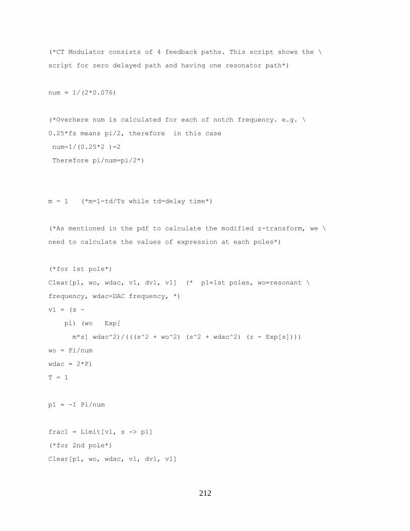
212
(*CT Modulator consists of 4 feedback paths. This script shows the \
script for zero delayed path and having one resonator path*)
num = 1/(2*0.076)
(*Overhere num is calculated for each of notch frequency. e.g. \
0.25*fs means pi/2, therefore in this case
num=1/(0.25*2 )=2
Therefore pi/num=pi/2*)
m = 1 (*m=1-td/Ts while td=delay time*)
(*As mentioned in the pdf to calculate the modified z-transform, we \
need to calculate the values of expression at each poles*)
(*for 1st pole*)
Clear[p1, wo, wdac, v1, dv1, v1] (* p1=1st poles, wo=resonant \
frequency, wdac=DAC frequency, *)
v1 = (s -
p1) (wo Exp[
m*s] wdac^2)/(((s^2 + wo^2) (s^2 + wdac^2) (z - Exp[s])))
wo = Pi/num
wdac = 2*Pi
T = 1
p1 = -I Pi/num
frac1 = Limit[v1, s -> p1]
(*for 2nd pole*)
Clear[p1, wo, wdac, v1, dv1, v1]
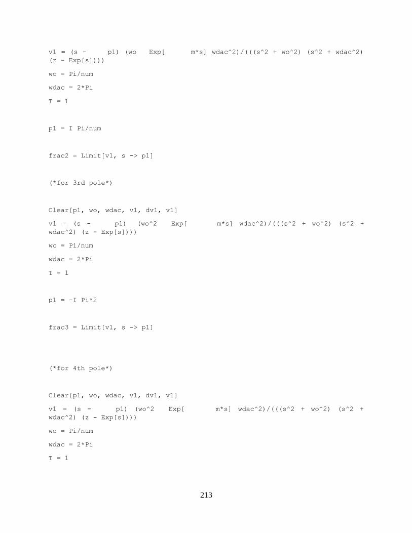
213
v1 = (s - p1) (wo Exp[ m*s] wdac^2)/(((s^2 + wo^2) (s^2 + wdac^2)
(z - Exp[s])))
wo = Pi/num
wdac = 2*Pi
T = 1
p1 = I Pi/num
frac2 = Limit[v1, s -> p1]
(*for 3rd pole*)
Clear[p1, wo, wdac, v1, dv1, v1]
v1 = (s - p1) (wo^2 Exp[ m*s] wdac^2)/(((s^2 + wo^2) (s^2 +
wdac^2) (z - Exp[s])))
wo = Pi/num
wdac = 2*Pi
T = 1
p1 = -I Pi*2
frac3 = Limit[v1, s -> p1]
(*for 4th pole*)
Clear[p1, wo, wdac, v1, dv1, v1]
v1 = (s - p1) (wo^2 Exp[ m*s] wdac^2)/(((s^2 + wo^2) (s^2 +
wdac^2) (z - Exp[s])))
wo = Pi/num
wdac = 2*Pi
T = 1
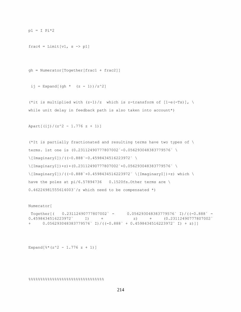
214
p1 = I Pi*2
frac4 = Limit[v1, s -> p1]
gh = Numerator[Together[frac1 + frac2]]
ij = Expand[(gh * (z - 1))/z^2]
(*it is multiplied with (z-1)/z which is z-transform of [1-e(-Ts)], \
while unit delay in feedback path is also taken into account*)
Apart[(ij)/(z^2 - 1.776 z + 1)]
(*It is partially fractionated and resulting terms have two types of \
terms. 1st one is (0.23112490777807002`-0.056293048383779576` \
\[ImaginaryI])/((-0.888`-0.4598434516223972` \
\[ImaginaryI])+z)+(0.23112490777807002`+0.056293048383779576` \
\[ImaginaryI])/((-0.888`+0.4598434516223972` \[ImaginaryI])+z) which \
have the poles at pi/6.57894736 0.1520fs.Other terms are \
0.46224981555614003`/z which need to be compensated *)
Numerator[
Together[( 0.23112490777807002` - 0.056293048383779576` I)/((-0.888` -
0.4598434516223972` I) + z) + (0.23112490777807002`
+ 0.056293048383779576` I)/((-0.888` + 0.4598434516223972` I) + z)]]
Expand[%*(z^2 - 1.776 z + 1)]
%%%%%%%%%%%%%%%%%%%%%%%%%%%%%%%%
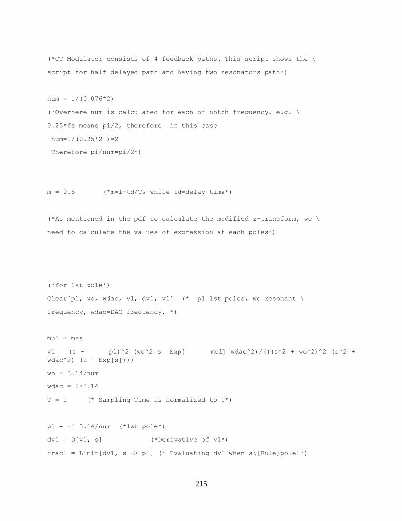
215
(*CT Modulator consists of 4 feedback paths. This script shows the \
script for half delayed path and having two resonators path*)
num = 1/(0.076*2)
(*Overhere num is calculated for each of notch frequency. e.g. \
0.25*fs means pi/2, therefore in this case
num=1/(0.25*2 )=2
Therefore pi/num=pi/2*)
m = 0.5 (*m=1-td/Ts while td=delay time*)
(*As mentioned in the pdf to calculate the modified z-transform, we \
need to calculate the values of expression at each poles*)
(*for 1st pole*)
Clear[p1, wo, wdac, v1, dv1, v1] (* p1=1st poles, wo=resonant \
frequency, wdac=DAC frequency, *)
mul = m*s
v1 = (s - p1)^2 (wo^2 s Exp[ mul] wdac^2)/(((s^2 + wo^2)^2 (s^2 +
wdac^2) (z - Exp[s])))
wo = 3.14/num
wdac = 2*3.14
T = 1 (* Sampling Time is normalized to 1*)
p1 = -I 3.14/num (*1st pole*)
dv1 = D[v1, s] (*Derivative of v1*)
frac1 = Limit[dv1, s -> p1] (* Evaluating dv1 when s\[Rule]pole1*)
216
(*for 2nd pole*)
Clear[p1, wo, wdac, v1, dv1, v1]
v1 = (s - p1)^2 (wo^2 s Exp[ mul] wdac^2)/(((s^2 + wo^2)^2 (s^2 +
wdac^2) (z - Exp[s])))
wo = 3.14/num
wdac = 2*3.14
T = 1
p1 = I 3.14/num
dv1 = D[v1, s]
frac2 = Limit[dv1, s -> p1]
(*for 3rd pole*)
Clear[p1, wo, wdac, v1, dv1, v1]
v1 = (s - p1) (wo^2 s Exp[ mul] wdac^2)/(((s^2 + wo^2)^2 (s^2 +
wdac^2) (z - Exp[s])))
wo = 3.14/num
wdac = 2*3.14
T = 1
p1 = -I 3.14*2
frac3 = Limit[v1, s -> p1]
(*for 4th pole*)
Clear[p1, wo, wdac, v1, dv1, v1]
v1 = (s -
p1) (wo^2 s Exp[ mul] wdac^2)/(((s^2 + wo^2)^2 (s^2 + wdac^2) (z -
Exp[s])))
wo = 3.14/num
wdac = 2*3.14
217
T = 1
p1 = I 3.14*2
frac4 = Limit[v1, s -> p1]
gh34 = Numerator[ Together[frac3 + frac4]] (* Numerator of
combination of 3rd and 4th \
fractions *)
gh = Numerator[ Together[frac1 + frac2]] (* Numerator
of combination of 1st and \
2nd fractions *)
den = Denominator[ Together[frac1 + frac2]] (* Denominator
of combination of 1st and 2nd \
fractions *)
(*Numerator of 3rd and 4th fractions is (0.005843299525388367`+0.` \
\[ImaginaryI])-(0.005843299525388367`+0.` \[ImaginaryI]) z it may be \
written as -0.005843299525388367*(z-1)*)
ij34 = (-0.005843306936293634*(z^2 - 1.776 z + 1)^2)/z^2
(*As frac1+frac2 =(-0.005843299525388367*(z-1))/((-1+z) ((-1+z) we \
multiply it (z-1)/z which is z-transform of [1-e(-Ts)], while unit \
delay in feedback path is also taken into account here.Moreover it \
is multiplied and divided with (z^2-1.776z+1)^2. Resultant is ij34*)
ij = Expand[(gh * (z - 1))/z^2]
(*frac3+frac4 is combined and then multiplied with (z-1)/z which is \

218
z-transform of [1-e(-Ts)],*)
afo = Apart[(ij34 + ij)/(z^2 - 1.776 z + 1)^2]
(*All of the fractions are combined and then partially fractionated. \
Resultant terms consist of two types of terms. One
is [(0.05674223809011536`+6.106226635438361`*^-16 \
\[ImaginaryI])/((-0.888`-0.4598434516223972` \
\[ImaginaryI])+z)^2-(0.10458793378536996`+0.07857423430477051` \
\[ImaginaryI])/((-0.888`-0.4598434516223972` \
\[ImaginaryI])+z)+(0.05674223809011464`+1.1102230246251565`*^-16 \
\[ImaginaryI])/((-0.888`+0.4598434516223972` \
\[ImaginaryI])+z)^2-(0.10458793378536854`-0.0785742343047709` \
\[ImaginaryI])/((-0.888`+0.4598434516223972` \[ImaginaryI])+z)],
that only shows the fractions having poles at \
pi/6.57894736 0.1520fs. Other terms are \
0.01684786921342306`/z^2+0.2091758675707385`/z which need to be \
compensated*)
Together[( 0.05674223809011536` + 6.106226635438361`*^-16 I)/((-0.888` -
0.4598434516223972` I) + z)^2 - (0.10458793378536996` +
0.07857423430477051` I)/((-0.888` - 0.4598434516223972` I) + z) + (
0.05674223809011464` + 1.1102230246251565`*^-16 I)/((-0.888` +
0.4598434516223972` I) + z)^2 - ( 0.10458793378536854` -
0.0785742343047709` I)/((-0.888` + 0.4598434516223972` I) + z)]
6.57895
0.5

219
0.5 s
(E^(0.5 s) s (-p1 + s)^2 wdac^2 wo^2)/((s^2 + wdac^2) (s^2 +
wo^2)^2 (-E^s + z))
0.47728
6.28
1
-0.47728 I
(8.98392 E^(1.5 s)
s (0.47728 I + s)^2)/((0.227796 + s^2)^2 (39.4384 + s^2) (-E^s +
z)^2) - (
17.9678 E^(0.5 s)
s^2 (0.47728 I + s)^2)/((0.227796 + s^2)^2 (39.4384 +
s^2)^2 (-E^s + z)) - (
35.9357 E^(0.5 s)
s^2 (0.47728 I + s)^2)/((0.227796 + s^2)^3 (39.4384 + s^2) (-E^s +
z)) + (17.9678 E^(0.5 s)
s (0.47728 I + s))/((0.227796 + s^2)^2 (39.4384 + s^2) (-E^s +
z)) + (8.98392 E^(
0.5 s) (0.47728 I + s)^2)/((0.227796 + s^2)^2 (39.4384 +
s^2) (-E^s + z)) + (
4.49196 E^(0.5 s)
s (0.47728 I + s)^2)/((0.227796 + s^2)^2 (39.4384 + s^2) (-E^s + z))
(0.0415874 + I (0.0433568 + 0.0589967 z) +
0.0113456 z)/((-0.888248 + 0.459365 I) + z)^2

220
(E^(0.5 s) s (-p1 + s)^2 wdac^2 wo^2)/((s^2 + wdac^2) (s^2 +
wo^2)^2 (-E^s + z))
0.47728
6.28
1
0.47728 I
(8.98392 E^(1.5 s)
s (-0.47728 I + s)^2)/((0.227796 + s^2)^2 (39.4384 + s^2) (-E^s +
z)^2) - (
17.9678 E^(0.5 s)
s^2 (-0.47728 I + s)^2)/((0.227796 + s^2)^2 (39.4384 +
s^2)^2 (-E^s + z)) - (
35.9357 E^(0.5 s)
s^2 (-0.47728 I + s)^2)/((0.227796 + s^2)^3 (39.4384 + s^2) (-E^s +
z)) + (17.9678 E^(0.5 s)
s (-0.47728 I + s))/((0.227796 + s^2)^2 (39.4384 + s^2) (-E^s +
z)) + (8.98392 E^(
0.5 s) (-0.47728 I + s)^2)/((0.227796 + s^2)^2 (39.4384 +
s^2) (-E^s + z)) + (
4.49196 E^(0.5 s)
s (-0.47728 I + s)^2)/((0.227796 + s^2)^2 (39.4384 + s^2) (-E^s +
z))
(0.0415874 + I (-0.0433568 - 0.0589967 z) +
0.0113456 z)/((-0.888248 - 0.459365 I) + z)^2

221
(E^(0.5 s) s (-p1 + s) wdac^2 wo^2)/((s^2 + wdac^2) (s^2 +
wo^2)^2 (-E^s + z))
0.47728
6.28
1
-6.28 I
-((0.00292165 + 4.65318*10^-6 I)/((-0.999995 - 0.0031853 I) + z))
(E^(0.5 s) s (-p1 + s) wdac^2 wo^2)/((s^2 + wdac^2) (s^2 +
wo^2)^2 (-E^s + z))
0.47728
6.28
1
6.28 I
-((0.00292165 - 4.65318*10^-6 I)/((-0.999995 + 0.0031853 I) + z))
(0.0058433 + 0. I) - (0.0058433 + 0. I) z
(-0.0226912 +
0. I) - (0.151268 + 0. I) z + (0.151268 + 0. I) z^2 + (0.0226912 +
0. I) z^3

222
((-0.888248 - 0.459365 I) + z)^2 ((-0.888248 + 0.459365 I) + z)^2
-((0.00584331 (1 - 1.776 z + z^2)^2)/z^2)
(-0.302536 + 0. I) + (0.0226912 + 0. I)/z^2 + (
0.128577 + 0. I)/z + (0.128577 + 0. I) z + (0.0226912 + 0. I) z^2
(0.0567422 + 6.10623*10^-16 I)/((-0.888 - 0.459843 I) + z)^2 - (
0.104588 + 0.0785742 I)/((-0.888 - 0.459843 I) + z) + (
0.0567422 + 1.11022*10^-16 I)/((-0.888 + 0.459843 I) + z)^2 - (
0.104588 - 0.0785742 I)/((-0.888 + 0.459843 I) + z) + (
0.0168479 - 6.93889*10^-17 I)/z^2 + (0.209176 - 3.88578*10^-16 I)/z
((0.323502 -
1.17961*10^-15 I) - (0.868953 - 1.56819*10^-15 I) z + (0.742993 -
9.99201*10^-16 I) z^2 - (0.209176 -
3.88578*10^-16 I) z^3)/(((-0.888 - 0.459843 I) +
z)^2 ((-0.888 + 0.459843 I) + z)^2)
afo
(0.0567422 + 6.10623*10^-16 I)/((-0.888 - 0.459843 I) + z)^2 - (
0.104588 + 0.0785742 I)/((-0.888 - 0.459843 I) + z) + (
0.0567422 + 1.11022*10^-16 I)/((-0.888 + 0.459843 I) + z)^2 - (
0.104588 - 0.0785742 I)/((-0.888 + 0.459843 I) + z) + (
0.0168479 - 6.93889*10^-17 I)/z^2 + (0.209176 - 3.88578*10^-16 I)/z
Chop[%]
0.0567422/((-0.888 - 0.459843 I) + z)^2 - (
0.104588 + 0.0785742 I)/((-0.888 - 0.459843 I) +
z) + 0.0567422/((-0.888 + 0.459843 I) + z)^2 - (

223
0.104588 - 0.0785742 I)/((-0.888 + 0.459843 I) +
z) + 0.0168479/z^2 + 0.209176/z
%%%%%%%%%%%%%%%%%%%%%%%%%%%%%%%%%%%%%%%%%%%
(*CT Modulator consists of 4 feedback paths. This script shows the \
script for zero delayed path and having two resonators path*)
num = 1/(0.076*2)
(*Overhere num is calculated for each of notch frequency. e.g. \
0.25*fs means pi/2, therefore in this case
num=1/(0.25*2 )=2
Therefore pi/num=pi/2*)
m = 1 (*m=1-td/Ts while td=delay time*)
(*As mentioned in the pdf to calculate the modified z-transform, we \
need to calculate the values of expression at each poles*)
(*for 1st pole*)
Clear[p1, wo, wdac, v1, dv1, v1] (* p1=1st poles, wo=resonant \
frequency, wdac=DAC frequency, *)
mul = m*s
v1 = (s -
p1)^2 (wo^2 s Exp[
mul] wdac^2)/(((s^2 + wo^2)^2 (s^2 + wdac^2) (z - Exp[s])))
wo = 3.14/num
wdac = 2*3.14
T = 1 (* Sampling Time is normalized to 1*)
p1 = -I 3.14/num (*1st pole*)
dv1 = D[v1, s] (*Derivative of v1*)
frac1 = Limit[dv1, s -> p1] (* Evaluating dv1 when s\[Rule]pole1*)
(*for 2nd pole*)
Clear[p1, wo, wdac, v1, dv1, v1]
v1 = (s -
p1)^2 (wo^2 s Exp[
mul] wdac^2)/(((s^2 + wo^2)^2 (s^2 + wdac^2) (z - Exp[s])))
wo = 3.14/num
wdac = 2*3.14
T = 1
p1 = I 3.14/num
dv1 = D[v1, s]
frac2 = Limit[dv1, s -> p1]

224
(*for 3rd pole*)
Clear[p1, wo, wdac, v1, dv1, v1]
v1 = (s -
p1) (wo^2 s Exp[
mul] wdac^2)/(((s^2 + wo^2)^2 (s^2 + wdac^2) (z - Exp[s])))
wo = 3.14/num
wdac = 2*3.14
T = 1
p1 = -I 3.14*2
frac3 = Limit[v1, s -> p1]
(*for 4th pole*)
Clear[p1, wo, wdac, v1, dv1, v1]
v1 = (s -
p1) (wo^2 s Exp[
mul] wdac^2)/(((s^2 + wo^2)^2 (s^2 + wdac^2) (z - Exp[s])))
wo = 3.14/num
wdac = 2*3.14
T = 1
p1 = I 3.14*2
frac4 = Limit[v1, s -> p1]
gh34 = Numerator[
Together[frac3 +
frac4]] (* Numerator of combination of 3rd and 4th \
fractions *)
gh = Numerator[
Together[frac1 +
frac2]] (* Numerator of combination of 1st and \
2nd fractions *)
den = Denominator[
Together[frac1 +
frac2]] (* Denominator of combination of 1st and 2nd \
fractions *)
(*Numerator of 3rd and 4th fractions is (0.005843299525388367`+0.` \
\[ImaginaryI])-(0.005843299525388367`+0.` \[ImaginaryI]) z it may be \
written as -0.005843299525388367*(z-1)*)
ij34 = (0.005843306936293634*(z^2 - 1.776 z + 1)^2)/z^2
(*As frac1+frac2 =(-0.005843299525388367*(z-1))/((-1+z) ((-1+z) we \

225
multiply it (z-1)/z which is z-transform of [1-e(-Ts)], while unit \
delay in feedback path is also taken into account here. Moreover it \
is multiplied and divided with (z^2-1.776z+1)^2. Resultant is ij34*)
ij = Expand[(gh * (z - 1))/z^2]
(*frac3+frac4 is combined and then multiplied with (z-1)/z which is \
z-transform of [1-e(-Ts)],*)
afo = Apart[(ij34 + ij)/(z^2 - 1.776 z + 1)^2]
(*All of the fractions are combined and then partially fractionated. \
Resultant terms consist of two types of terms. One
is [(0.05674223809011536`+6.106226635438361`*^-16 \
\[ImaginaryI])/((-0.888`-0.4598434516223972` \
\[ImaginaryI])+z)^2-(0.10458793378536996`+0.07857423430477051` \
\[ImaginaryI])/((-0.888`-0.4598434516223972` \
\[ImaginaryI])+z)+(0.05674223809011464`+1.1102230246251565`*^-16 \
\[ImaginaryI])/((-0.888`+0.4598434516223972` \
\[ImaginaryI])+z)^2-(0.10458793378536854`-0.0785742343047709` \
\[ImaginaryI])/((-0.888`+0.4598434516223972` \[ImaginaryI])+z)],
that only shows the fractions having poles at \
pi/6.57894736 0.1520fs. Other terms are \
(0.01684786921342306`-6.938893903907228`*^-17 \
\[ImaginaryI])/z^2+(0.2091758675707385`-3.885780586188048`*^-16 \
\[ImaginaryI])/z which need to be compensated*)
Together[(
0.05513056690221478` +
0.01342766387430719` I)/((-0.888` - 0.4598434516223972` I) +
z)^2 - (0.055459239262580104` +
0.10780534574735412` I)/((-0.888` - 0.4598434516223972` I) + z) + (
0.05513056690221432` -
0.013427663874306857` I)/((-0.888` + 0.4598434516223972` I) +
z)^2 - (0.05545923926257927` -
0.10780534574735401` I)/((-0.888` + 0.4598434516223972` I) + z)]
226
APPENDIX B
Matlab Code for 4th
-Order Variable Notch Frequency CRFF ΣΔM ADC
close all
mex 'simulateDSM.c'
OSR=50; % Oversampling Ratio
N = 4; % Order of Modulator
H_inf=1.912; % Out of band gain
opt =1; % Zero Optimization
Nlev =4; % No of Levels =4 when used it relaxes the
% swing requirement
tun=0;
for (i=1:48)%%%% getting 100 NTF for 100 notch frequencies with step of
.0025*fs OSR = 40e6/(2*50e3); % OSR = 80
H(i) = synthesizeNTF(N,OSR,opt,H_inf,0.01*tun);
stf(i)=H(i); %copy the ntf to stf, so that they will have the same poles.
stf(i).z=[]; %setting the numerator of stf to 1
tun=i;
end
p=13;
H=H(p);
form = 'CRFF';
% Plot the response with chosen coefficients
[a,g,b,c] = realizeNTF(H,'CRFF')
ABCD = stuffABCD(a,g,b,c,form);
[ntf, stf] = calculateTF(ABCD);
f = linspace(0,0.24,1000);
z = exp(2i*pi*f);
magNTF = dbv(evalTF(ntf,z));
magSTF = dbv(evalTF(stf,z));

227
subplot(224)
figure
plot(f,magNTF,'b',f,magSTF,'m','LineWidth',1)
xlabel('Normalized Frequency');
ylabel('Magnitude');
legend('Noise Transfer Function','Signal TransferFunction')
%%%%%%%%%%%%%% Part 2 -- Perform Dynamic Range Scaling %%%%%%%%%%%%%
u = linspace(0,(Nlev-1),100);
Np = 1e4; % Number of same input points to test at time
T = ones(1,Np); %Normalized input signal = 5 (Nlev)
maxima = zeros(N,length(u));
for i = 1:length(u)
ui = u(i);
[v,xn,xmax] = simulateDSM( ui(T), ABCD, Nlev );
% Get Values for the max of each output node
maxima(:,i) = xmax(:);
if any(xmax>1e2) % Why100 ???
umax = ui % MaxStable input (Only stable to 2.88)
u = u(1:i);
maxima = maxima(:,1:i);
break;
end
end
figure; clf
for i = 1:N
plot(u,maxima(i,:),'o');
if i==1
hold on;
end
plot(u,maxima(i,:),'g-','linewidth',2);

228
end
axis([0 3 0 10])
xlabel('Input Amplitude (Max = 5)')
ylabel('State Amplitude (Max = 5)')
x = [0.84 0.77 1.01 1.24]
[ABCDs,umax] = scaleABCD(ABCD,Nlev,0.01*(p-1),x,Nlev+5,[],Np)
[as,gs,bs,cs] = mapABCD(ABCDs,form)
u = linspace(0,umax,100);
for i = 1:length(u)
ui = u(i);
[v,xn,xmax] = simulateDSM( ui(T), ABCDs,Nlev );
maxima(:,i) = xmax(:);
if any(xmax>1e2)
umax = ui;
u = u(1:i);
maxima = maxima(:,1:i);
break;
end
end
%figure; clf
for i = 1:N
%plot(u,maxima(i,:),'ro');
if i==1
hold on;
end
plot(u,maxima(i,:),'k-','linewidth',3);
axis([0 3 0 5])
xlabel('Input Amplitude (Max = 5)')
ylabel('State Amplitude (Max = 5)')
%legend('Pre-Dynamic Range Scaling','','','Post-Dynamic Range Scaling')
end

229
%%%%%%%%%%%%%%%%%%%%%%%%%%%%%%%%%%%%%%%%%%%%%%%%%%%%%%%%%%%%%%%%%%%%%%%%%%%%%
%%%%%%%%%%%%%%%%%%%%%%%
%%%%%%%%%% Part 7 - "Quantise" The Cap Values%%%%%%%%%%
R = 100; % Rounding Factor
a2 = round([as].*R)./R
%gsn = gs;
g2 = round([gs].*R)./R
b2 = round([bs].*R)./R
c2 = round([cs].*R)./R
asn_f(p,:)=a2
gsn_f(p,:)= g2
bsn_f(p,:)=b2
csn_f(p,:)=c2
fs=100e6;fi=0.01*(p-1)*fs;A=1;ts=1/fs;Ts=1/fs;N=65536 ;i=1 % Simulation
Parameters
sigma=0.05 % Coefficients Uncertainty
sim('wbbpsdm_old.mdl')