
A statistical methodology for the design of high-performance CMOScurrent-steering digital-to-analog...
18
IEEE TRANSACTIONS ON COMPUTER-AIDED DESIGN OF INTEGRATED CIRCUITS AND SYSTEMS, VOL. 21, NO. 4, APRIL 2002 377 A Statistical Methodology for the Design of High-Performance CMOS Current-Steering Digital-to-Analog Converters Paolo Crippa, Member, IEEE, Claudio Turchetti, Member, IEEE, and Massimo Conti, Member, IEEE Abstract—With the shrinking of device sizes, random device variations become a key factor limiting the performances of high-resolution complementary metal–oxide–semiconductor (CMOS) current-steering digital-to-analog converters (DACs). In this paper, we present a novel design methodology based on statistical modeling of MOS transistor drain current that allows designers to explore different DAC architectures and to study the effects of technological variations on system performance without using time-consuming Monte Carlo simulations. This technique requires as a first step the estimation of the mean value and the autocorrelation function of a single stochastic process. This sto- chastic process models the device drain current and summarizes all the random sources associated with the process/device varia- tions since the current represents the effect of all of them. Subse- quently, on the basis of such an approach, a behavioral model of current-steering DACs has been developed. Finally, the statistical simulation of static performances such as differential nonlinearity and integral nonlinearity has been carried out for different DAC architectures based on the behavioral model previously derived. Index Terms—Behavioral modeling, CMOS, current-steering, digital-to-analog converters, mismatch, statistical variations. I. INTRODUCTION T HE RAPID growth in the markets of wired and wireless communications systems has been forcing integrated circuit (IC) producers to integrate both digital and analog sections on a single chip. As a consequence, the design of high-performance digital-to-analog/analog-to-digital interfaces for use in these systems is becoming a challenging task. In particular, high-definition television (HDTV), digital mobile phones (GSM), and high-speed internet access (xDSL) all need digital-to-analog converters (DACs) meeting high-accuracy as well as high-speed and low-power performance requirements. Complementary metal–oxide–semiconductor (CMOS) DACs based on current-steering architectures are often used for these applications since they do not need large silicon areas for their implementation and they can be integrated easily in fully digital CMOS technologies. In addition, since these architectures can directly drive resistive loads, they do not require high-speed am- plifiers at the output, thus resulting potentially faster than other types of DACs [1]. Manuscript received January 26, 2001; revised November 12, 2001. This work was supported in part by the Consiglio Nazionale delle Ricerche (CNR), Italy, Progetto Finalizzato MADESS-II. This paper was recommended by Ed- itor-in-Chief K. Mayaram. The authors are with the Dipartimento di Elettronica e Automatica, Uni- versity of Ancona, I-60131 Ancona, Italy (e-mail: [email protected]; [email protected]; [email protected]). Publisher Item Identifier S 0278-0070(02)02477-6. Current-steering DACs are based on arrays of cells orga- nized into unary- (thermometer) -encoded or binary-weighted elements that are steered to the DAC output depending on the digital input code. New segmented current-steering topologies have recently been designed that benefit from the advantages of both binary-coded and thermometer-coded architectures, resulting in faster and more linear DACs. In such topologies, the least significant bits steer binary-weighted current sources, while the most significant bits are thermometer-encoded and steer a unary current source array [2]–[6]. As current-steering DACs use several identical building blocks (current sources), their performances depend on the statistical variability of the devices constituting them. With the submicrometer geometries used nowadays in very large scale integration (VLSI) technologies, accurate modeling of the statistical behavior of integrated devices thus becomes essential to the design of high-resolution CMOS DACs [6]–[14]. One effect requiring accurate modeling is the MOS transistor mismatch, namely the effect that causes a dependence of corre- lation among parameters of identical transistors on their mutual distance, so that identically designed devices display different statistical behaviors [15]–[21]. This dependence is due to the nonuniformity of process parameters, which are sources of sta- tistical variations in the die that must be seen as random func- tions of position in the die [15]–[17], [22]. Designing high-per- formance DACs thus requires a thorough understanding of the relationships between performance and source of technological errors to obtain a larger effective number of bits as in high-res- olution DACs. Performance sensitivity to mismatch error can be reduced by exploiting the statistical behavior of the error sources, in particular their dependence on position in the die, which can direct the choice of a layout that minimizes the mis- match effect [6]. In this paper, we present a statistical methodology for the design of high-performance CMOS current-steering D/A con- verters, which is able to evaluate the performance of different DAC architectures without using a time-consuming Monte Carlo approach. The methodology is based on 1) a simple MOSFET model that summarizes all the random sources associated with the process/device variations, and 2) a specific behavioral DAC model for some classes of architectures. The simple statistical MOSFET model, which predicts a random variability superimposed on the model used for nom- inal (i.e., not inclusive of statistical effects) circuit simulation, simplifies the characterization and simulation stages while affording good accuracy for both inter- and intra-die parameter variations. 0278-0070/02$17.00 © 2002 IEEE
-
Upload
independent -
Category
Documents
-
view
1 -
download
0
Transcript of A statistical methodology for the design of high-performance CMOScurrent-steering digital-to-analog...
IEEE TRANSACTIONS ON COMPUTER-AIDED DESIGN OF INTEGRATED CIRCUITS AND SYSTEMS, VOL. 21, NO. 4, APRIL 2002 377
A Statistical Methodology for the Design ofHigh-Performance CMOS Current-Steering
Digital-to-Analog ConvertersPaolo Crippa, Member, IEEE, Claudio Turchetti, Member, IEEE, and Massimo Conti, Member, IEEE
Abstract—With the shrinking of device sizes, random devicevariations become a key factor limiting the performances ofhigh-resolution complementary metal–oxide–semiconductor(CMOS) current-steering digital-to-analog converters (DACs).
In this paper, we present a novel design methodology based onstatistical modeling of MOS transistor drain current that allowsdesigners to explore different DAC architectures and to study theeffects of technological variations on system performance withoutusing time-consuming Monte Carlo simulations. This techniquerequires as a first step the estimation of the mean value and theautocorrelation function of a single stochastic process. This sto-chastic process models the device drain current and summarizesall the random sources associated with the process/device varia-tions since the current represents the effect of all of them. Subse-quently, on the basis of such an approach, a behavioral model ofcurrent-steering DACs has been developed. Finally, the statisticalsimulation of static performances such as differential nonlinearityand integral nonlinearity has been carried out for different DACarchitectures based on the behavioral model previously derived.
Index Terms—Behavioral modeling, CMOS, current-steering,digital-to-analog converters, mismatch, statistical variations.
I. INTRODUCTION
T HE RAPID growth in the markets of wired and wirelesscommunications systems has been forcing integrated
circuit (IC) producers to integrate both digital and analogsections on a single chip. As a consequence, the design ofhigh-performance digital-to-analog/analog-to-digital interfacesfor use in these systems is becoming a challenging task. Inparticular, high-definition television (HDTV), digital mobilephones (GSM), and high-speed internet access (xDSL) all needdigital-to-analog converters (DACs) meeting high-accuracy aswell as high-speed and low-power performance requirements.
Complementary metal–oxide–semiconductor (CMOS) DACsbased on current-steering architectures are often used for theseapplications since they do not need large silicon areas for theirimplementation and they can be integrated easily in fully digitalCMOS technologies. In addition, since these architectures candirectly drive resistive loads, they do not require high-speed am-plifiers at the output, thus resulting potentially faster than othertypes of DACs [1].
Manuscript received January 26, 2001; revised November 12, 2001. Thiswork was supported in part by the Consiglio Nazionale delle Ricerche (CNR),Italy, Progetto Finalizzato MADESS-II. This paper was recommended by Ed-itor-in-Chief K. Mayaram.
The authors are with the Dipartimento di Elettronica e Automatica, Uni-versity of Ancona, I-60131 Ancona, Italy (e-mail: [email protected];[email protected]; [email protected]).
Publisher Item Identifier S 0278-0070(02)02477-6.
Current-steering DACs are based on arrays of cells orga-nized into unary- (thermometer) -encoded or binary-weightedelements that are steered to the DAC output depending on thedigital input code. New segmented current-steering topologieshave recently been designed that benefit from the advantagesof both binary-coded and thermometer-coded architectures,resulting in faster and more linear DACs. In such topologies,the least significant bits steer binary-weighted current sources,while the most significant bits are thermometer-encoded andsteer a unary current source array [2]–[6].
As current-steering DACs use several identical buildingblocks (current sources), their performances depend on thestatistical variability of the devices constituting them. Withthe submicrometer geometries used nowadays in very largescale integration (VLSI) technologies, accurate modeling of thestatistical behavior of integrated devices thus becomes essentialto the design of high-resolution CMOS DACs [6]–[14].
One effect requiring accurate modeling is the MOS transistormismatch, namely the effect that causes a dependence of corre-lation among parameters of identical transistors on their mutualdistance, so that identically designed devices display differentstatistical behaviors [15]–[21]. This dependence is due to thenonuniformity of process parameters, which are sources of sta-tistical variations in the die that must be seen as random func-tions of position in the die [15]–[17], [22]. Designing high-per-formance DACs thus requires a thorough understanding of therelationships between performance and source of technologicalerrors to obtain a larger effective number of bits as in high-res-olution DACs. Performance sensitivity to mismatch error canbe reduced by exploiting the statistical behavior of the errorsources, in particular their dependence on position in the die,which can direct the choice of a layout that minimizes the mis-match effect [6].
In this paper, we present a statistical methodology for thedesign of high-performance CMOS current-steering D/A con-verters, which is able to evaluate the performance of differentDAC architectures without using a time-consuming MonteCarlo approach. The methodology is based on1) a simpleMOSFET model that summarizes all the random sourcesassociated with the process/device variations, and2) a specificbehavioral DAC model for some classes of architectures.
The simple statistical MOSFET model, which predicts arandom variability superimposed on the model used for nom-inal (i.e., not inclusive of statistical effects) circuit simulation,simplifies the characterization and simulation stages whileaffording good accuracy for both inter- and intra-die parametervariations.
0278-0070/02$17.00 © 2002 IEEE
378 IEEE TRANSACTIONS ON COMPUTER-AIDED DESIGN OF INTEGRATED CIRCUITS AND SYSTEMS, VOL. 21, NO. 4, APRIL 2002
As for as DAC performances is concerned, they can be di-vided into static, namelydifferential nonlinearity(DNL) andin-tegral nonlinearity(INL) and dynamic, such as signal-to-noiseratio (SNR), total harmonic distortion (THD), spurious-free dy-namic range (SFDR), and signal-to-noise-and-distortion ratio(SNDR). On the one hand, good static performances can beachieved by taking into account all possible random, system-atic and graded errors and accurately designing a circuit layoutaimed at reducing them. On the other hand, for telecommuni-cations applications dynamic performances play a critical rolein DAC quality. Dynamic performances can be characterizedby the dynamic nonlinearities associated with current sourceswitching. They are determined by signal-dependent errors suchas nonlinear slewing, imperfect synchronization of the inputsignal of the current switches, glitches, and settling errors. Thesedynamic nonlinearities are mainly reduced by adopting circuitalsolutions that exceed the scope of this work. Thus, this paperaddresses DAC static performances only without any concernto dynamic performances.
To this end, a set of generic equations for describing the sta-tistical behavior of DACs is derived. These equations can becharacterized for a given DAC architecture. Statistical simula-tion efficiency is significantly improved by using these equa-tions. A preferred architecture of a DAC can be selected bycomparing the simulation results on various architectures anddifferent floor plans.
The paper is organized as follows. A statistical model of draincurrent is suggested in Section II. The model is defined as anerror source superimposed on the nominal drain current. Sec-tion III describes the methodology adopted for estimating themodel from experimental data. Section IV states the problemof statistical simulation of DAC performances. Section V re-ports mathematical models of DNL and INL as functions oferror sources for different DAC architectures. The descriptionof a tool for statistical simulation and some application exam-ples are reported in Section VI. Finally, some conclusions arediscussed in Section VII.
II. M ISMATCH MODELING
In this section, we suggest a simple statistical MOS transistormodel where, unlike the usual models in which statistical varia-tions are related to the random parameters in the nominal currentmodel, the random behavior due to deviation in the manufac-turing process is superimposed on the model used for nominalcircuit simulation (which ignores random fluctuations). As amain result, the characterization, modeling, and simulation pro-cedures are greatly simplified.
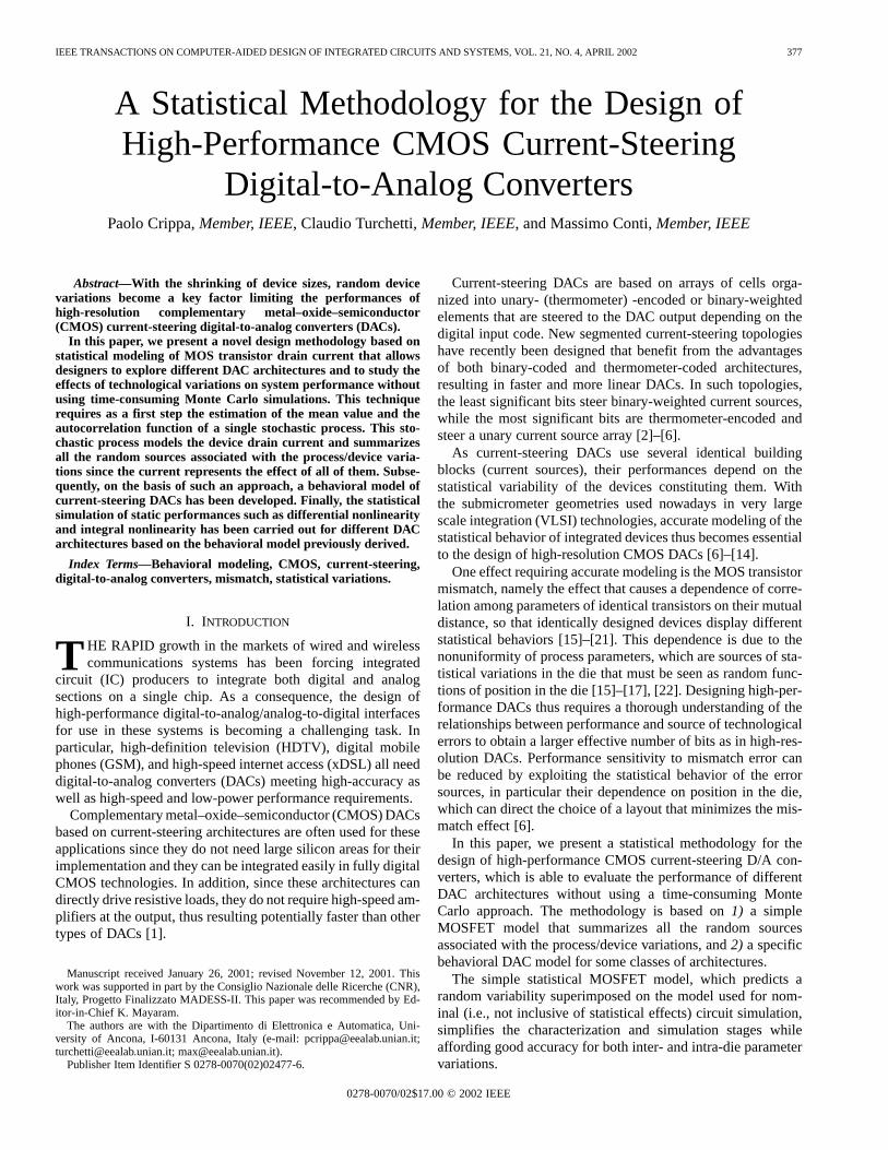
We assume that the mismatch effect can be modeled as anerror source coupled in parallel with the nominal current ,as shown in Fig. 1, so that the total drain currentis given by
(1)
The nonrandom term represents the usual dc drain current,whereas the term gives rise to some random fluctuationsaround that depend on device position in the wafer, theregion of operation of the device and its dimensionsand .
Fig. 1. Error source.
On the basis of these considerations, the following simplemodel will be assumed
(2)
where the term , depending on the voltage vector, takes into account the operating region (being
a fitting parameter to be estimated from experimental data),takes into account the dependence on dimensions and
summarizes all the sources of error depending on de-vice position in the die. In this way, bothinter-die (die-to-die,wafer-to-wafer, lot-to-lot) andintra-die (mismatch) variationsof all device parameters can be lumped in the term. Indeed, as
models the device drain current, which is affected by severalrandom process/device variations, it summarizes these randomsources because the current represents the effect of all of them.
If represents the wafer surface and the parameterstands for the device position in the die, then can
be considered as aspatial stochastic process, namely as a familyof real-value random variables indexed by thetwo-dimensional (2-D) variable [23]. It is worth noting thatfrom (2) follows that the processis not only dependent on thecoordinates ( ), but also on bias and device size.
If the process is assumed to be aGaussianprocess defined by the property that all finite subsets
are jointly normal, it iscompletely characterized by its mean value and covariancefunction [24]. However, also in the general case of anon-Gaussian process, a partial characterization of theprocess (up to the second-order momenta) will be sufficient,because this is all that is required for statistical simulation,as explained below in the section devoted to the theory ofstatistical simulation.
Given , the covariance function of theprocess is defined as
(3)
where the notation represents the expectation ofthe random variable . Let be a wide-sensestationary processwith zero mean value, as customaryin mismatch modeling. In this case, and
, where, . As a consequence, the derived
stochastic processgiven by (2) is also a zero-mean wide-sensestationary process.
CRIPPAet al.: STATISTICAL METHODOLOGY FOR THE DESIGN OF CMOS CURRENT-STEERING DACs 379
In a circuit with devices placed in different positions in thedie, the following sources of error result
(4)These error sources are random variables representingreal-izations of the stochastic process. Their covariance matrix isdefined as an matrix whose generic th term is given by
(5)
Since the terms are nonrandom, they can be ex-tracted from the expected value operator as multiplying factorsso that from (5) and (3), one obtains
(6)
By defining the diagonal matrix as
(7)and (6) can be rewritten in matrix form
(8)
being a function of the voltage vector andthe vectors of device dimensions ,
and being a function of devicecoordinates , . Thus, from(8) there clearly appears a dependence of the covariance matrix
on device position ( ) in addition to the bias voltagevector and device sizes and .
Rewriting (1) as
(9)
where the stochastic processes and have andzero-mean values respectively, it results
(10)
i.e., the covariance function of is the same as the autocorre-lation function of . By combining (10) and (5), (8) becomes:
(11)
Equation (11) is of central importance since it relates the co-variance of the current to the covariance of the error source
so as a model for can be derived once a mathematicalmodel for has been assumed.
A common choice for is a Gaussian function, namely,for a stationary process
(12)
where , and are fitting parameters and ,are distances between a pair of devices along the
- and -axes, respectively. As a consequence, predicts adependence on ( ) as well as on voltages and device dimen-sions.
The geometry dependence ofrepresented in (2) byresults from the fact that the drain current is affected by thestatistical parameters (i.e., gate oxide thickness, doping level,etc.) that are distributed over the whole active area of the de-vice [16], [17], [19]. As usually assumed in the mismatch mod-eling of single device parameters [18], [19], at short correlationdistances the absolute value of these effects is inversely propor-tional to the square root of this area. Therefore, it is reasonableto assume for the random fluctuationsa depen-dence, i.e.
(13)
where is an additional fitting parameter. Despite its first-order nature, such a dependence on device size is quite reason-able, since statistical current variability decreases for larger de-vices, representing a good tradeoff between approximation ac-curacy and simplicity of the drain current model.
As a result, if the Gaussian function in (12) has been assumedfor , the covariance function becomes
(14)
where , , , and have to be estimated from mea-surements. The model (14) relates the covariance function oferror sources to bias conditions, device dimensions and posi-tion in the die, and has the following properties:1) it dependson the Euclidean distance between two points;2) it attains itsmaximum when the distance is zero;3) it tends to vanish as thedistance approaches to infinity; and4) it tends to vanish as de-vice size increases. These properties are quite reasonable basedon the physical intuition of mismatch phenomena.
By denoting with the inverse of matrix (which mustexist, since is diagonal), (11) can be solved for
(15)
allowing to derive from experimental current data.
III. M ODEL ESTIMATION FROM EXPERIMENTAL DATA
A. Test Pattern and Measurement Methodology
A test pattern with different-sized transistors arranged inarrays of identical transistors was designed to estimate this sta-tistical drain current model. Assuming an array with rowsand columns, drain currents may be measured ineach array for several bias conditions.
Adequate data for estimation can be gathered by choosingseveral aspect ratios for both NMOS and PMOS transistors:
, 5/1.4, 2/1, 1/0.7, 0.7/0.5, 0.5/0.35, 1/1, 0.7/1,0.5/1 m m. Thus, 18 arrays of 8 8 cascode transistor pairswere designed in a single die, one for each geometry. Finally,
380 IEEE TRANSACTIONS ON COMPUTER-AIDED DESIGN OF INTEGRATED CIRCUITS AND SYSTEMS, VOL. 21, NO. 4, APRIL 2002
Fig. 2. Transistor array and decoding scheme.
39 replicas of the die were implemented on an 8-in wafer manu-factured with 0.35-m single poly and five metal layers CMOStechnology. The schematic of a single array together with therow and column decoders for selecting one transistor at a timeare shown in Fig. 2.
Measurements were performed using a high-precision com-puter-controlled measurement system consisting of:1) a semi-automatic probe station enabling massive measurements of dieson the wafer;2) a switching matrix for driving the decoding/se-lection bus;3) an HP4145B semiconductor parameter analyzerfor dc curve measurement; and4) a host workstation with a spe-cific software for the experimental characterization.
Measurements were taken at ambient temperature; however,the wafer being tested was kept at C C by a regulatedchuck to avoid temperature fluctuations during measurements.Overall system accuracy was checked by making over 100 con-secutive measurement runs on the same transistor, obtaining astandard deviation of drain current of less than 0.03%. The tran-sistors in the arrays were measured sequentially: for each ge-ometry and several bias conditions, 64 drain currents were mea-sured. Transistor drain currents in the arrays were measured di-rectly on the wafer using the semiautomatic probe station. Eachdata is the mean of 16 samples using a feature of the HP4145B.
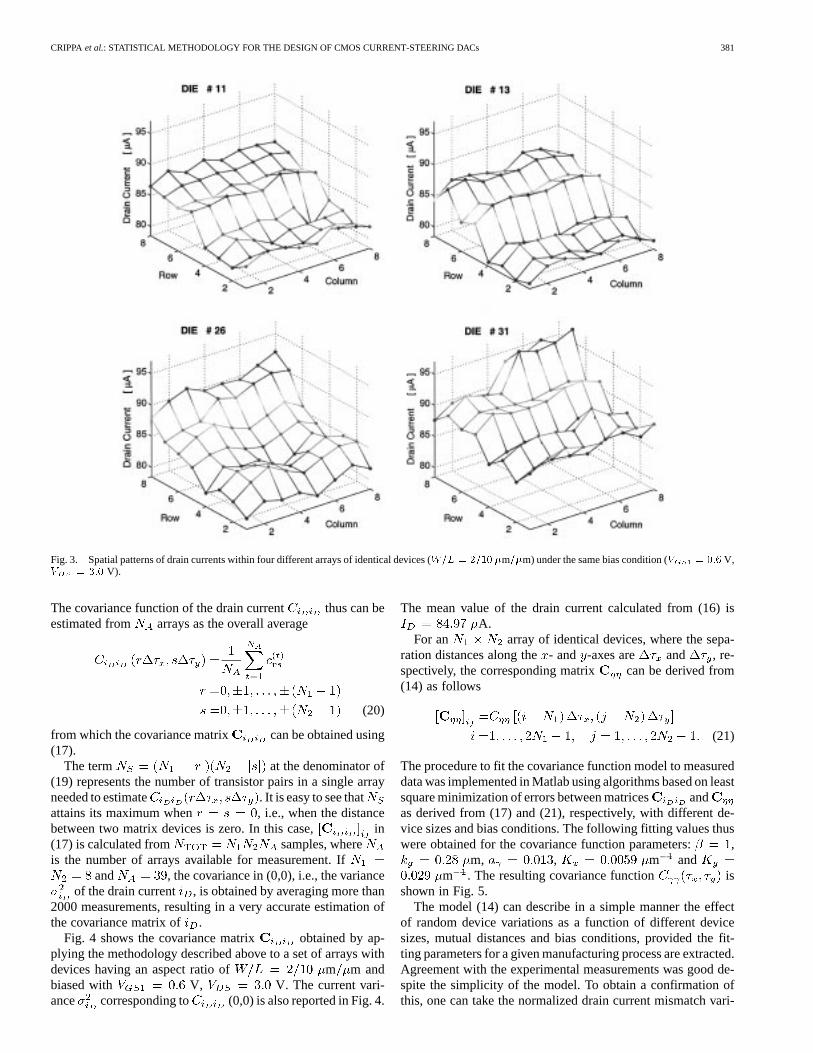
The spatial pattern of drain currents within six different ar-rays for the same bias condition is shown in Figs. 3(a)–(f) asan example. Each point of the mesh represents the drain cur-rent measured from a device placed at the same point of the griddomain. The devices in these arrays have the same geometry( m m) and operate in the saturation regionwith V and V.
Due to statistical tolerance effects (on oxide thickness and/ordoping concentrations), identical transistors under the same biasconditions exhibit different drain currents (intra-die mismatch),whereas transistors belonging to different arrays but placed inthe same relative position behave differently (Fig. 3).
It is worth noting that, regardless of the array considered, thecurrent shows the typical behavior of a linear gradient due toglobal variations (long correlation distance) and a superimposedwhite noise due to local variations (short correlation distance).
B. Model Characterization
As explained in Section II, if is assumed to be aGaussian stochastic process, it is completely characterized by
its mean value and covariance function. The same propertyholds for the process because it is related to by (2).This assumption might appear to reduce model accuracy; infact, as will be clearer below, accurate statistical simulationof DAC performances only requires knowing the covariancefunction of the process and its mean value, which is alsoneeded for the nominal (or deterministic) simulation. The aimof this section is thus to derive relationships for the meanand the covariance matrix as functions of the measuredcurrent values.
Once the measurements of the arrays are performed, a dis-crete spatial current indexed by , and is obtained,
being the drain current of the device placed inth posi-tion of the th array.
By assuming that or, which is the same, , isa wide-sense stationary process, the mean value of the draincurrent can be considered as being independent of the positionacross the wafer, i.e., .
One suitable method to estimate is to use the average ofthe values over the total number ofdevices, i.e.
(16)
Thus, can be considered as the expected value of MOSFETdrain current for any device in a given bias condition and geom-etry regardless of its position across the wafer. Moreover,is the deterministic value of a MOS transistor drain current asusually calculated from models in which all parameters are in-dependent of position.
The th element of the covariance matrix of draincurrents is defined as the covariance functionevaluated in the grid of a generic array, i.e.,
(17)
where and are the separation distances in theanddirections between adjacent devices of the array. It is worth
noting that an transistor array will yield a matrixof dimensions .
Based on the definition of covariance, for two devices placedat points ( ) and ( ) in a single array, the covari-ance of their drain currents is
(18)
which can be estimated as the average
(19)with , ,
and .
CRIPPAet al.: STATISTICAL METHODOLOGY FOR THE DESIGN OF CMOS CURRENT-STEERING DACs 381
Fig. 3. Spatial patterns of drain currents within four different arrays of identical devices (W=L = 2=10 �m=�m) under the same bias condition (V = 0:6 V,V = 3:0 V).
The covariance function of the drain current thus can beestimated from arrays as the overall average
(20)
from which the covariance matrix can be obtained using(17).
The term at the denominator of(19) represents the number of transistor pairs in a single arrayneeded to estimate . It is easy to see thatattains its maximum when , i.e., when the distancebetween two matrix devices is zero. In this case, in(17) is calculated from samples, whereis the number of arrays available for measurement. If
and , the covariance in (0,0), i.e., the varianceof the drain current , is obtained by averaging more than
2000 measurements, resulting in a very accurate estimation ofthe covariance matrix of .
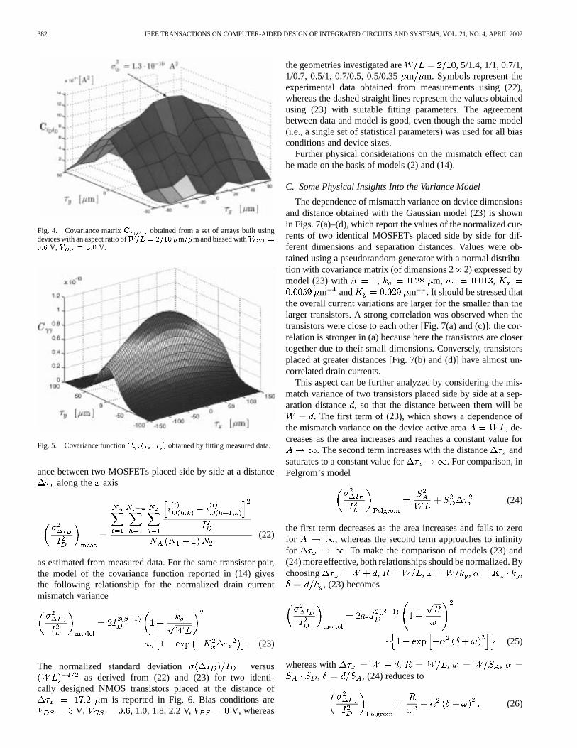
Fig. 4 shows the covariance matrix obtained by ap-plying the methodology described above to a set of arrays withdevices having an aspect ratio of m m andbiased with V, V. The current vari-ance corresponding to (0,0) is also reported in Fig. 4.
The mean value of the drain current calculated from (16) isA.
For an array of identical devices, where the sepa-ration distances along the- and -axes are and , re-spectively, the corresponding matrix can be derived from(14) as follows
(21)
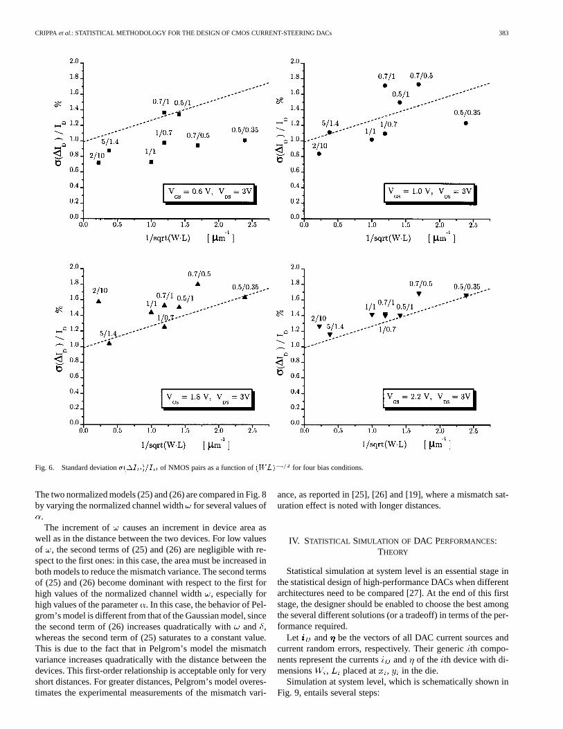
The procedure to fit the covariance function model to measureddata was implemented in Matlab using algorithms based on leastsquare minimization of errors between matrices andas derived from (17) and (21), respectively, with different de-vice sizes and bias conditions. The following fitting values thuswere obtained for the covariance function parameters: ,
m, , m andm . The resulting covariance function is
shown in Fig. 5.The model (14) can describe in a simple manner the effect
of random device variations as a function of different devicesizes, mutual distances and bias conditions, provided the fit-ting parameters for a given manufacturing process are extracted.Agreement with the experimental measurements was good de-spite the simplicity of the model. To obtain a confirmation ofthis, one can take the normalized drain current mismatch vari-
382 IEEE TRANSACTIONS ON COMPUTER-AIDED DESIGN OF INTEGRATED CIRCUITS AND SYSTEMS, VOL. 21, NO. 4, APRIL 2002
Fig. 4. Covariance matrixC obtained from a set of arrays built usingdevices with an aspect ratio ofW=L = 2=10�m=�m and biased withV =0:6 V, V = 3:0 V.
Fig. 5. Covariance functionC (� ; � ) obtained by fitting measured data.
ance between two MOSFETs placed side by side at a distancealong the axis
(22)
as estimated from measured data. For the same transistor pair,the model of the covariance function reported in (14) givesthe following relationship for the normalized drain currentmismatch variance
(23)
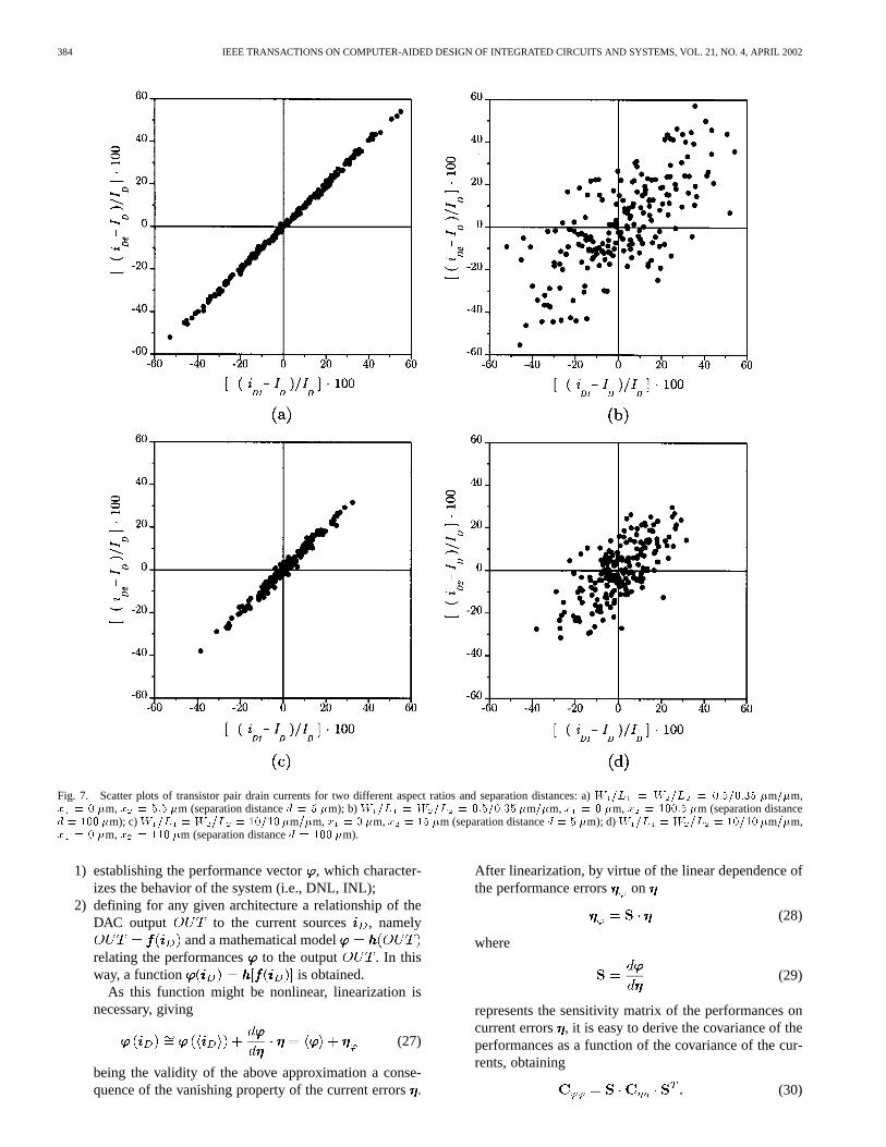
The normalized standard deviation versusas derived from (22) and (23) for two identi-
cally designed NMOS transistors placed at the distance ofm is reported in Fig. 6. Bias conditions are
V, , 1.0, 1.8, 2.2 V, V, whereas
the geometries investigated are , 5/1.4, 1/1, 0.7/1,1/0.7, 0.5/1, 0.7/0.5, 0.5/0.35m m. Symbols represent theexperimental data obtained from measurements using (22),whereas the dashed straight lines represent the values obtainedusing (23) with suitable fitting parameters. The agreementbetween data and model is good, even though the same model(i.e., a single set of statistical parameters) was used for all biasconditions and device sizes.
Further physical considerations on the mismatch effect canbe made on the basis of models (2) and (14).
C. Some Physical Insights Into the Variance Model
The dependence of mismatch variance on device dimensionsand distance obtained with the Gaussian model (23) is shownin Figs. 7(a)–(d), which report the values of the normalized cur-rents of two identical MOSFETs placed side by side for dif-ferent dimensions and separation distances. Values were ob-tained using a pseudorandom generator with a normal distribu-tion with covariance matrix (of dimensions 22) expressed bymodel (23) with , m, ,
m and m . It should be stressed thatthe overall current variations are larger for the smaller than thelarger transistors. A strong correlation was observed when thetransistors were close to each other [Fig. 7(a) and (c)]: the cor-relation is stronger in (a) because here the transistors are closertogether due to their small dimensions. Conversely, transistorsplaced at greater distances [Fig. 7(b) and (d)] have almost un-correlated drain currents.
This aspect can be further analyzed by considering the mis-match variance of two transistors placed side by side at a sep-aration distance , so that the distance between them will be
. The first term of (23), which shows a dependence ofthe mismatch variance on the device active area , de-creases as the area increases and reaches a constant value for
. The second term increases with the distance andsaturates to a constant value for . For comparison, inPelgrom’s model
(24)
the first term decreases as the area increases and falls to zerofor , whereas the second term approaches to infinityfor . To make the comparison of models (23) and(24) more effective, both relationships should be normalized. Bychoosing , , , ,
, (23) becomes
(25)
whereas with , , ,, , (24) reduces to
(26)
CRIPPAet al.: STATISTICAL METHODOLOGY FOR THE DESIGN OF CMOS CURRENT-STEERING DACs 383
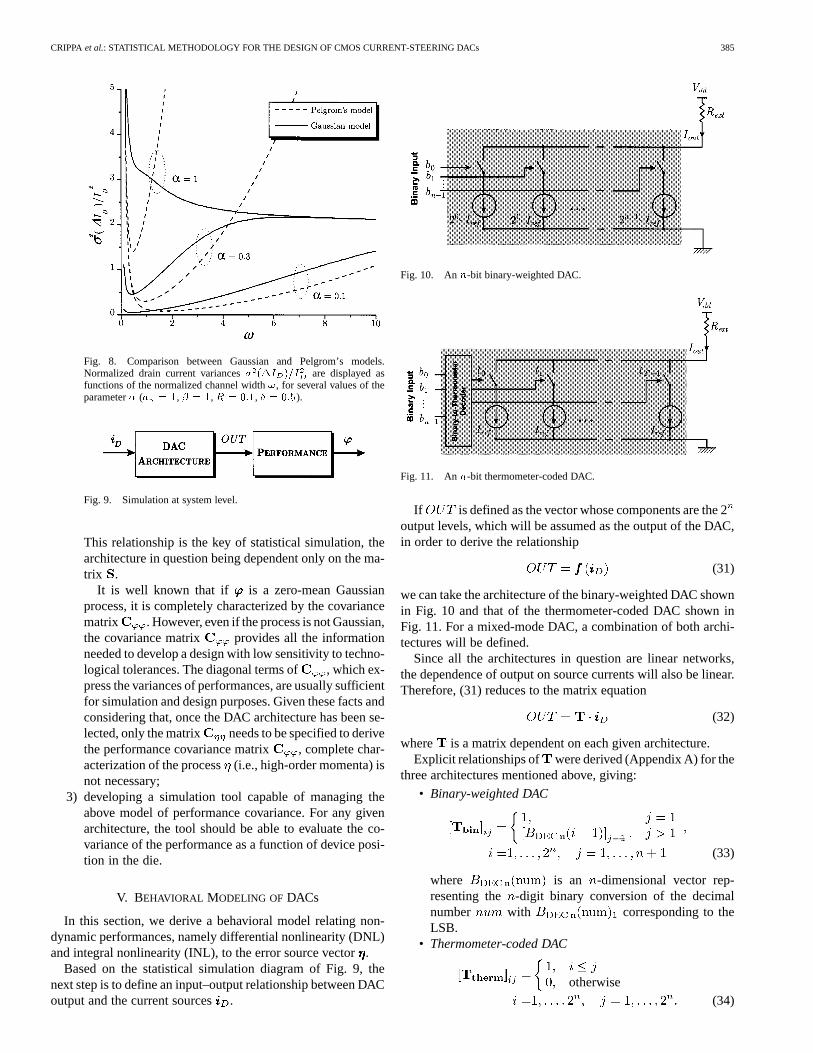
Fig. 6. Standard deviation�(�I )=I of NMOS pairs as a function of(WL) for four bias conditions.
The two normalized models (25) and (26) are compared in Fig. 8by varying the normalized channel widthfor several values of
.The increment of causes an increment in device area as
well as in the distance between the two devices. For low valuesof , the second terms of (25) and (26) are negligible with re-spect to the first ones: in this case, the area must be increased inboth models to reduce the mismatch variance. The second termsof (25) and (26) become dominant with respect to the first forhigh values of the normalized channel width, especially forhigh values of the parameter. In this case, the behavior of Pel-grom’s model is different from that of the Gaussian model, sincethe second term of (26) increases quadratically withand ,whereas the second term of (25) saturates to a constant value.This is due to the fact that in Pelgrom’s model the mismatchvariance increases quadratically with the distance between thedevices. This first-order relationship is acceptable only for veryshort distances. For greater distances, Pelgrom’s model overes-timates the experimental measurements of the mismatch vari-
ance, as reported in [25], [26] and [19], where a mismatch sat-uration effect is noted with longer distances.
IV. STATISTICAL SIMULATION OF DAC PERFORMANCES:THEORY
Statistical simulation at system level is an essential stage inthe statistical design of high-performance DACs when differentarchitectures need to be compared [27]. At the end of this firststage, the designer should be enabled to choose the best amongthe several different solutions (or a tradeoff) in terms of the per-formance required.
Let and be the vectors of all DAC current sources andcurrent random errors, respectively. Their genericth compo-nents represent the currents and of the th device with di-mensions , placed at , in the die.
Simulation at system level, which is schematically shown inFig. 9, entails several steps:
384 IEEE TRANSACTIONS ON COMPUTER-AIDED DESIGN OF INTEGRATED CIRCUITS AND SYSTEMS, VOL. 21, NO. 4, APRIL 2002
Fig. 7. Scatter plots of transistor pair drain currents for two different aspect ratios and separation distances: a)W =L = W =L = 0:5=0:35 �m=�m,x = 0 �m, x = 5:5 �m (separation distanced = 5 �m); b)W =L = W =L = 0:5=0:35 �m=�m,x = 0 �m, x = 100:5 �m (separation distanced = 100 �m); c)W =L =W =L = 10=10 �m=�m,x = 0 �m,x = 15 �m (separation distanced = 5 �m); d)W =L =W =L = 10=10�m=�m,x = 0 �m, x = 110 �m (separation distanced = 100 �m).
1) establishing the performance vector, which character-izes the behavior of the system (i.e., DNL, INL);
2) defining for any given architecture a relationship of theDAC output to the current sources , namely
and a mathematical modelrelating the performances to the output . In thisway, a function is obtained.
As this function might be nonlinear, linearization isnecessary, giving
(27)
being the validity of the above approximation a conse-quence of the vanishing property of the current errors.
After linearization, by virtue of the linear dependence ofthe performance errors on
(28)
where
(29)
represents the sensitivity matrix of the performances oncurrent errors , it is easy to derive the covariance of theperformances as a function of the covariance of the cur-rents, obtaining
(30)
CRIPPAet al.: STATISTICAL METHODOLOGY FOR THE DESIGN OF CMOS CURRENT-STEERING DACs 385
Fig. 8. Comparison between Gaussian and Pelgrom’s models.Normalized drain current variances� (�I )=I are displayed asfunctions of the normalized channel width!, for several values of theparameter� (a = 1, � = 1, R = 0:1, � = 0:5).
Fig. 9. Simulation at system level.
This relationship is the key of statistical simulation, thearchitecture in question being dependent only on the ma-trix .
It is well known that if is a zero-mean Gaussianprocess, it is completely characterized by the covariancematrix . However, even if the process is not Gaussian,the covariance matrix provides all the informationneeded to develop a design with low sensitivity to techno-logical tolerances. The diagonal terms of , which ex-press the variances of performances, are usually sufficientfor simulation and design purposes. Given these facts andconsidering that, once the DAC architecture has been se-lected, only the matrix needs to be specified to derivethe performance covariance matrix , complete char-acterization of the process(i.e., high-order momenta) isnot necessary;
3) developing a simulation tool capable of managing theabove model of performance covariance. For any givenarchitecture, the tool should be able to evaluate the co-variance of the performance as a function of device posi-tion in the die.
V. BEHAVIORAL MODELING OF DACs
In this section, we derive a behavioral model relating non-dynamic performances, namely differential nonlinearity (DNL)and integral nonlinearity (INL), to the error source vector.
Based on the statistical simulation diagram of Fig. 9, thenext step is to define an input–output relationship between DACoutput and the current sources.
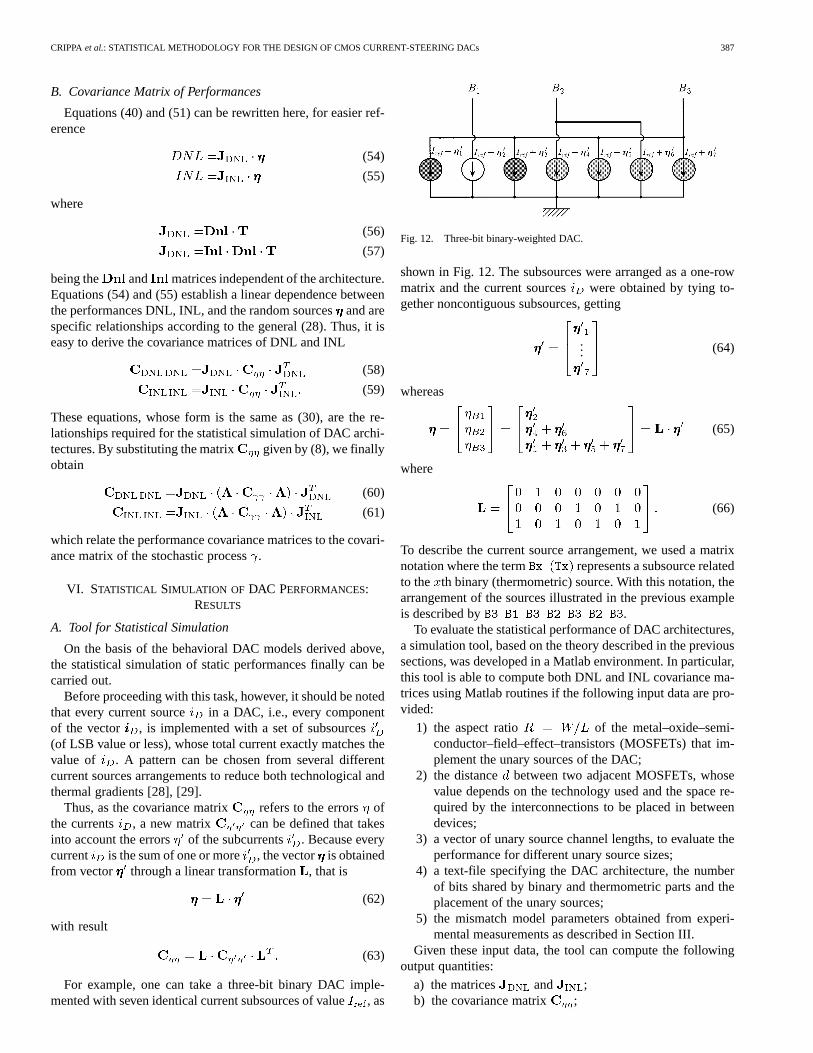
Fig. 10. Ann-bit binary-weighted DAC.
Fig. 11. Ann-bit thermometer-coded DAC.
If is defined as the vector whose components are the 2output levels, which will be assumed as the output of the DAC,in order to derive the relationship
(31)
we can take the architecture of the binary-weighted DAC shownin Fig. 10 and that of the thermometer-coded DAC shown inFig. 11. For a mixed-mode DAC, a combination of both archi-tectures will be defined.
Since all the architectures in question are linear networks,the dependence of output on source currents will also be linear.Therefore, (31) reduces to the matrix equation
(32)
where is a matrix dependent on each given architecture.Explicit relationships of were derived (Appendix A) for the
three architectures mentioned above, giving:
• Binary-weighted DAC
(33)
where is an -dimensional vector rep-resenting the -digit binary conversion of the decimalnumber with corresponding to theLSB.
• Thermometer-coded DAC
otherwise(34)
386 IEEE TRANSACTIONS ON COMPUTER-AIDED DESIGN OF INTEGRATED CIRCUITS AND SYSTEMS, VOL. 21, NO. 4, APRIL 2002
• Mixed-mode DAC
......
(35)
where is a matrix depending on the parameteras
otherwise(36)
and is a matrix with dimensionsdefined as in (33) with .
A. Nondynamic Performances
In order to obtain nondynamic performances, DNL and INL,as functions of , it is useful to derive the vector , whosecomponents are the random variables associated with the 2output levels. Combining (1) and (32), one obtains
(37)
1) DNL: DNL is the difference between the amplitude of theinput–output characteristic and the required value. Thus, wecan define a vector such that
(38)
where is an integer number between 1 and .Since , (38) canbe rewritten as:
(39)
Thus, the vector can be obtained as a linear transforma-tion of the vector
(40)
where is a matrix of dimensions whosegeneric th element is
otherwise(41)
and
(42)
2) INL: The vector can be derived in a similar wayas a function of the vector. Let be the number of bitsand the number of current sources adopted (the same numberas the error sources). INL is the difference between the actualinput–output characteristic and the straight line intersecting the
points and , defining the range of the DAC givenby:
(43)
The step size in the ideal case is
(44)
Thus, from the definition of INL, we have
(45)
To obtain the required relationship between and ,we use
(46)
and
(47)
which are derived in Appendix B. By substituting (46) and (47)into (45), we get
(48)
And in particular
(49)
whereas we assume
(50)
Equation (48) can be rewritten in matrix notation as
(51)
where is a matrix of dimensions whosegeneric -element is
(52)
and
(53)
Finally, it should be highlighted that the dimension of the vectordepends on the architecture chosen.
CRIPPAet al.: STATISTICAL METHODOLOGY FOR THE DESIGN OF CMOS CURRENT-STEERING DACs 387
B. Covariance Matrix of Performances
Equations (40) and (51) can be rewritten here, for easier ref-erence
(54)
(55)
where
(56)
(57)
being the and matrices independent of the architecture.Equations (54) and (55) establish a linear dependence betweenthe performances DNL, INL, and the random sourcesand arespecific relationships according to the general (28). Thus, it iseasy to derive the covariance matrices of DNL and INL
(58)
(59)
These equations, whose form is the same as (30), are the re-lationships required for the statistical simulation of DAC archi-tectures. By substituting the matrix given by (8), we finallyobtain
(60)
(61)
which relate the performance covariance matrices to the covari-ance matrix of the stochastic process.
VI. STATISTICAL SIMULATION OF DAC PERFORMANCES:RESULTS
A. Tool for Statistical Simulation
On the basis of the behavioral DAC models derived above,the statistical simulation of static performances finally can becarried out.
Before proceeding with this task, however, it should be notedthat every current source in a DAC, i.e., every componentof the vector , is implemented with a set of subsources(of LSB value or less), whose total current exactly matches thevalue of . A pattern can be chosen from several differentcurrent sources arrangements to reduce both technological andthermal gradients [28], [29].
Thus, as the covariance matrix refers to the errors ofthe currents , a new matrix can be defined that takesinto account the errors of the subcurrents . Because everycurrent is the sum of one or more , the vector is obtainedfrom vector through a linear transformation, that is
(62)
with result
(63)
For example, one can take a three-bit binary DAC imple-mented with seven identical current subsources of value, as
Fig. 12. Three-bit binary-weighted DAC.
shown in Fig. 12. The subsources were arranged as a one-rowmatrix and the current sources were obtained by tying to-gether noncontiguous subsources, getting
... (64)
whereas
(65)
where
(66)
To describe the current source arrangement, we used a matrixnotation where the term represents a subsource relatedto the th binary (thermometric) source. With this notation, thearrangement of the sources illustrated in the previous exampleis described by .
To evaluate the statistical performance of DAC architectures,a simulation tool, based on the theory described in the previoussections, was developed in a Matlab environment. In particular,this tool is able to compute both DNL and INL covariance ma-trices using Matlab routines if the following input data are pro-vided:
1) the aspect ratio of the metal–oxide–semi-conductor–field–effect–transistors (MOSFETs) that im-plement the unary sources of the DAC;
2) the distance between two adjacent MOSFETs, whosevalue depends on the technology used and the space re-quired by the interconnections to be placed in betweendevices;
3) a vector of unary source channel lengths, to evaluate theperformance for different unary source sizes;
4) a text-file specifying the DAC architecture, the numberof bits shared by binary and thermometric parts and theplacement of the unary sources;
5) the mismatch model parameters obtained from experi-mental measurements as described in Section III.
Given these input data, the tool can compute the followingoutput quantities:
a) the matrices and ;b) the covariance matrix ;
388 IEEE TRANSACTIONS ON COMPUTER-AIDED DESIGN OF INTEGRATED CIRCUITS AND SYSTEMS, VOL. 21, NO. 4, APRIL 2002
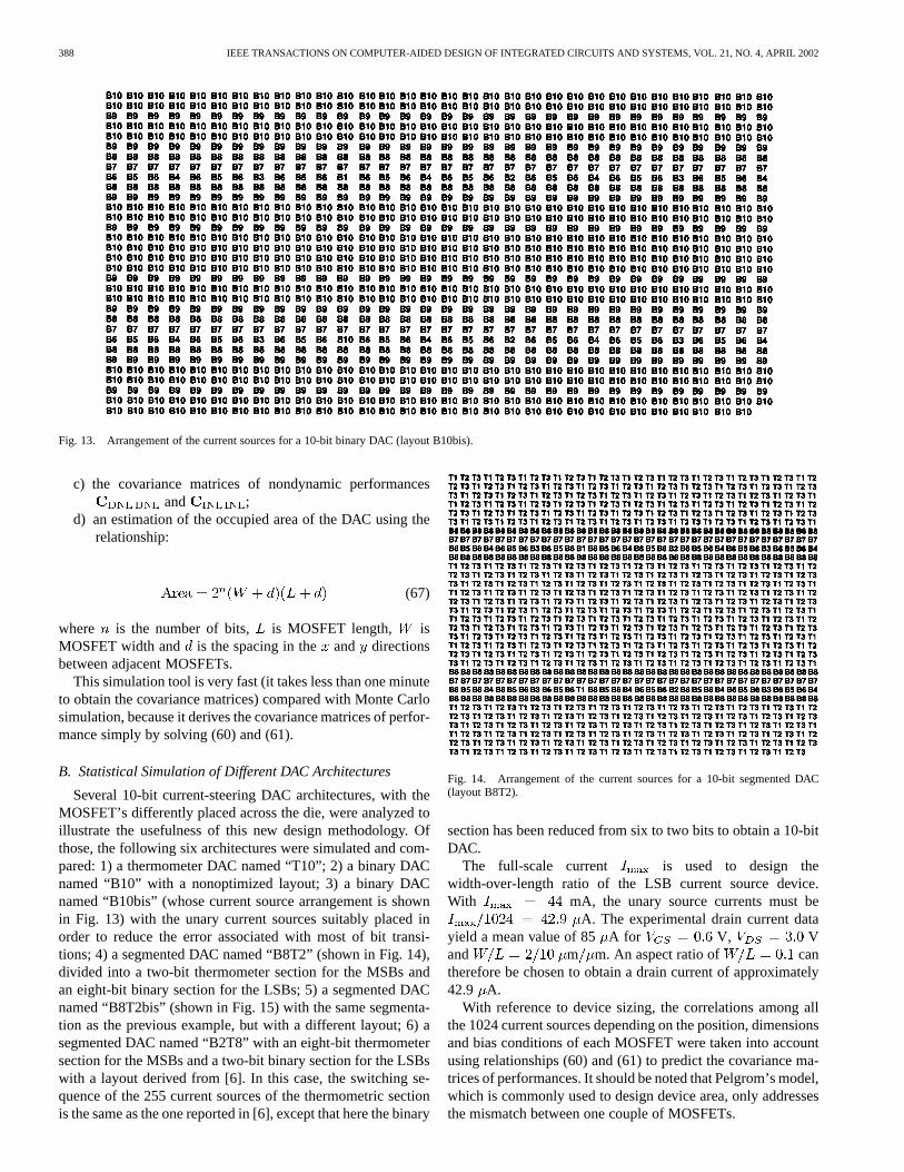
Fig. 13. Arrangement of the current sources for a 10-bit binary DAC (layout B10bis).
c) the covariance matrices of nondynamic performancesand ;
d) an estimation of the occupied area of the DAC using therelationship:
(67)
where is the number of bits, is MOSFET length, isMOSFET width and is the spacing in the and directionsbetween adjacent MOSFETs.
This simulation tool is very fast (it takes less than one minuteto obtain the covariance matrices) compared with Monte Carlosimulation, because it derives the covariance matrices of perfor-mance simply by solving (60) and (61).
B. Statistical Simulation of Different DAC Architectures
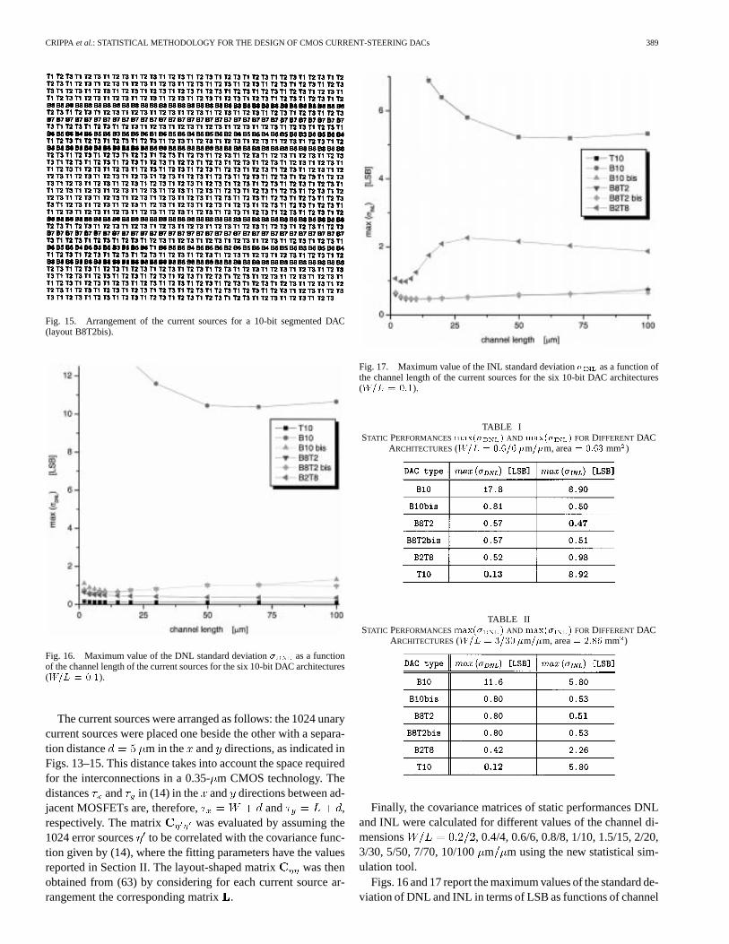
Several 10-bit current-steering DAC architectures, with theMOSFET’s differently placed across the die, were analyzed toillustrate the usefulness of this new design methodology. Ofthose, the following six architectures were simulated and com-pared: 1) a thermometer DAC named “T10”; 2) a binary DACnamed “B10” with a nonoptimized layout; 3) a binary DACnamed “B10bis” (whose current source arrangement is shownin Fig. 13) with the unary current sources suitably placed inorder to reduce the error associated with most of bit transi-tions; 4) a segmented DAC named “B8T2” (shown in Fig. 14),divided into a two-bit thermometer section for the MSBs andan eight-bit binary section for the LSBs; 5) a segmented DACnamed “B8T2bis” (shown in Fig. 15) with the same segmenta-tion as the previous example, but with a different layout; 6) asegmented DAC named “B2T8” with an eight-bit thermometersection for the MSBs and a two-bit binary section for the LSBswith a layout derived from [6]. In this case, the switching se-quence of the 255 current sources of the thermometric sectionis the same as the one reported in [6], except that here the binary
Fig. 14. Arrangement of the current sources for a 10-bit segmented DAC(layout B8T2).
section has been reduced from six to two bits to obtain a 10-bitDAC.
The full-scale current is used to design thewidth-over-length ratio of the LSB current source device.With mA, the unary source currents must be
A. The experimental drain current datayield a mean value of 85A for V, Vand m m. An aspect ratio of cantherefore be chosen to obtain a drain current of approximately42.9 A.
With reference to device sizing, the correlations among allthe 1024 current sources depending on the position, dimensionsand bias conditions of each MOSFET were taken into accountusing relationships (60) and (61) to predict the covariance ma-trices of performances. It should be noted that Pelgrom’s model,which is commonly used to design device area, only addressesthe mismatch between one couple of MOSFETs.
CRIPPAet al.: STATISTICAL METHODOLOGY FOR THE DESIGN OF CMOS CURRENT-STEERING DACs 389
Fig. 15. Arrangement of the current sources for a 10-bit segmented DAC(layout B8T2bis).
Fig. 16. Maximum value of the DNL standard deviation� as a functionof the channel length of the current sources for the six 10-bit DAC architectures(W=L = 0:1).
The current sources were arranged as follows: the 1024 unarycurrent sources were placed one beside the other with a separa-tion distance m in the and directions, as indicated inFigs. 13–15. This distance takes into account the space requiredfor the interconnections in a 0.35-m CMOS technology. Thedistances and in (14) in the and directions between ad-jacent MOSFETs are, therefore, and ,respectively. The matrix was evaluated by assuming the1024 error sources to be correlated with the covariance func-tion given by (14), where the fitting parameters have the valuesreported in Section II. The layout-shaped matrix was thenobtained from (63) by considering for each current source ar-rangement the corresponding matrix.
Fig. 17. Maximum value of the INL standard deviation� as a function ofthe channel length of the current sources for the six 10-bit DAC architectures(W=L = 0:1).
TABLE ISTATIC PERFORMANCESmax(� ) AND max(� ) FORDIFFERENTDAC
ARCHITECTURES(W=L = 0:6=6 �m=�m, area= 0:63 mm )
TABLE IISTATIC PERFORMANCESmax(� ) AND max(� ) FORDIFFERENTDAC
ARCHITECTURES(W=L = 3=30 �m=�m, area= 2:86 mm )
Finally, the covariance matrices of static performances DNLand INL were calculated for different values of the channel di-mensions , 0.4/4, 0.6/6, 0.8/8, 1/10, 1.5/15, 2/20,3/30, 5/50, 7/70, 10/100m m using the new statistical sim-ulation tool.
Figs. 16 and 17 report the maximum values of the standard de-viation of DNL and INL in terms of LSB as functions of channel
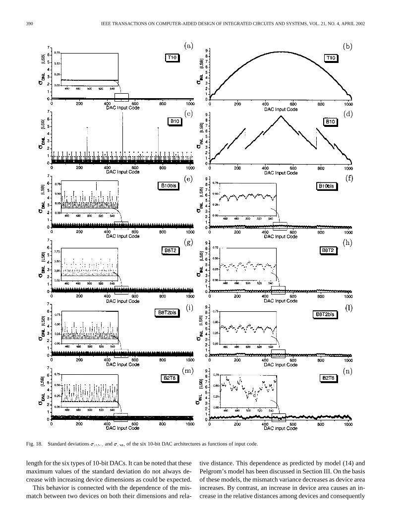
390 IEEE TRANSACTIONS ON COMPUTER-AIDED DESIGN OF INTEGRATED CIRCUITS AND SYSTEMS, VOL. 21, NO. 4, APRIL 2002
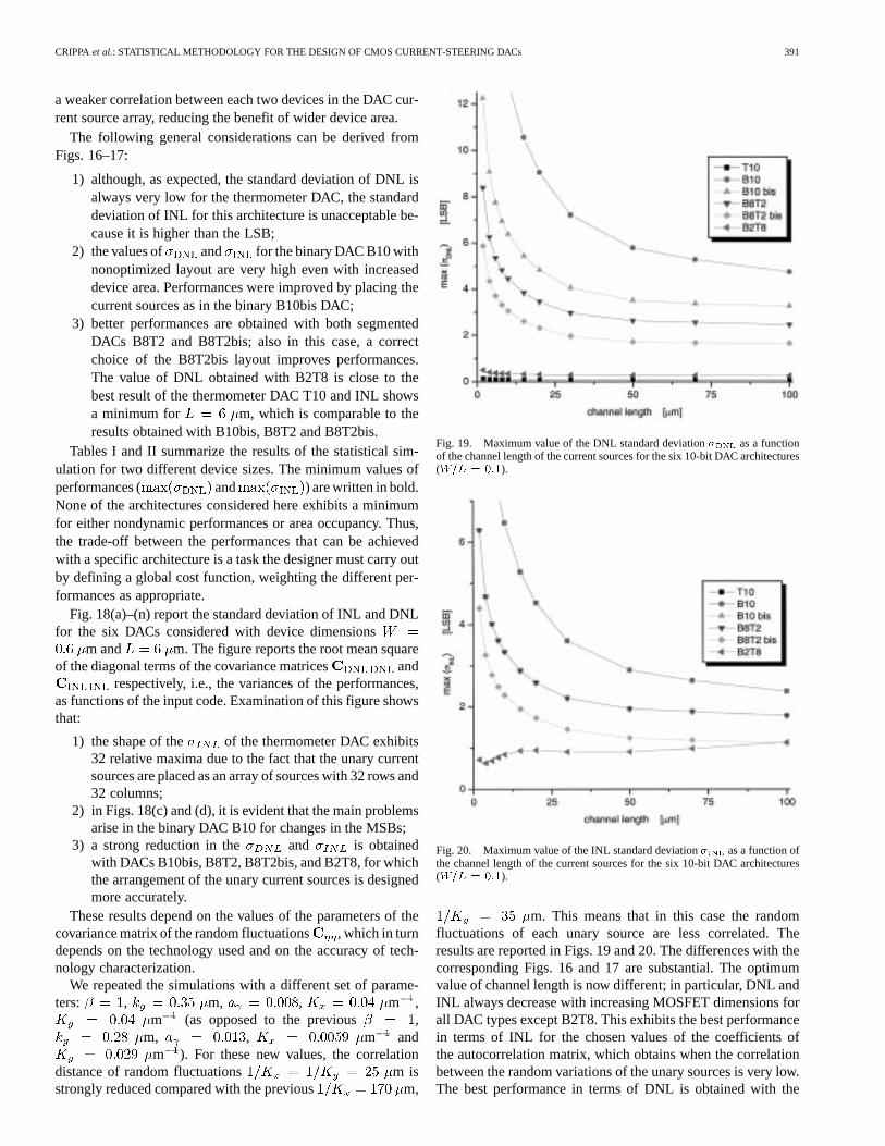
Fig. 18. Standard deviations� and� of the six 10-bit DAC architectures as functions of input code.
length for the six types of 10-bit DACs. It can be noted that thesemaximum values of the standard deviation do not always de-crease with increasing device dimensions as could be expected.
This behavior is connected with the dependence of the mis-match between two devices on both their dimensions and rela-
tive distance. This dependence as predicted by model (14) andPelgrom’s model has been discussed in Section III. On the basisof these models, the mismatch variance decreases as device areaincreases. By contrast, an increase in device area causes an in-crease in the relative distances among devices and consequently
CRIPPAet al.: STATISTICAL METHODOLOGY FOR THE DESIGN OF CMOS CURRENT-STEERING DACs 391
a weaker correlation between each two devices in the DAC cur-rent source array, reducing the benefit of wider device area.
The following general considerations can be derived fromFigs. 16–17:
1) although, as expected, the standard deviation of DNL isalways very low for the thermometer DAC, the standarddeviation of INL for this architecture is unacceptable be-cause it is higher than the LSB;
2) the values of and for the binary DAC B10 withnonoptimized layout are very high even with increaseddevice area. Performances were improved by placing thecurrent sources as in the binary B10bis DAC;
3) better performances are obtained with both segmentedDACs B8T2 and B8T2bis; also in this case, a correctchoice of the B8T2bis layout improves performances.The value of DNL obtained with B2T8 is close to thebest result of the thermometer DAC T10 and INL showsa minimum for m, which is comparable to theresults obtained with B10bis, B8T2 and B8T2bis.
Tables I and II summarize the results of the statistical sim-ulation for two different device sizes. The minimum values ofperformances ( and ) are written in bold.None of the architectures considered here exhibits a minimumfor either nondynamic performances or area occupancy. Thus,the trade-off between the performances that can be achievedwith a specific architecture is a task the designer must carry outby defining a global cost function, weighting the different per-formances as appropriate.
Fig. 18(a)–(n) report the standard deviation of INL and DNLfor the six DACs considered with device dimensions
m and m. The figure reports the root mean squareof the diagonal terms of the covariance matrices and
respectively, i.e., the variances of the performances,as functions of the input code. Examination of this figure showsthat:
1) the shape of the of the thermometer DAC exhibits32 relative maxima due to the fact that the unary currentsources are placed as an array of sources with 32 rows and32 columns;
2) in Figs. 18(c) and (d), it is evident that the main problemsarise in the binary DAC B10 for changes in the MSBs;
3) a strong reduction in the and is obtainedwith DACs B10bis, B8T2, B8T2bis, and B2T8, for whichthe arrangement of the unary current sources is designedmore accurately.
These results depend on the values of the parameters of thecovariance matrix of the random fluctuations , which in turndepends on the technology used and on the accuracy of tech-nology characterization.
We repeated the simulations with a different set of parame-ters: , m, , m ,
m (as opposed to the previous ,m, , m and
m ). For these new values, the correlationdistance of random fluctuations m isstrongly reduced compared with the previous m,
Fig. 19. Maximum value of the DNL standard deviation� as a functionof the channel length of the current sources for the six 10-bit DAC architectures(W=L = 0:1).
Fig. 20. Maximum value of the INL standard deviation� as a function ofthe channel length of the current sources for the six 10-bit DAC architectures(W=L = 0:1).
m. This means that in this case the randomfluctuations of each unary source are less correlated. Theresults are reported in Figs. 19 and 20. The differences with thecorresponding Figs. 16 and 17 are substantial. The optimumvalue of channel length is now different; in particular, DNL andINL always decrease with increasing MOSFET dimensions forall DAC types except B2T8. This exhibits the best performancein terms of INL for the chosen values of the coefficients ofthe autocorrelation matrix, which obtains when the correlationbetween the random variations of the unary sources is very low.The best performance in terms of DNL is obtained with the
392 IEEE TRANSACTIONS ON COMPUTER-AIDED DESIGN OF INTEGRATED CIRCUITS AND SYSTEMS, VOL. 21, NO. 4, APRIL 2002
thermometric DAC, but good results are also obtained with theB2T8. The optimum value of design parameters and in somecases also optimum DAC architecture, depends on the corre-lation distance; accurate characterization of the technologicalrandom variations as a function of device area and relativedistances is thus crucial to DAC design. The curves in Figs. 19and 20 clearly tend to saturate: the standard deviation of INLtends to a constant value for all layout styles and types of DAC,whereas the standard deviation of DNL tends to different valuesdepending on the type of DAC, albeit without a dependenceon layout style. In fact, as device dimensions tend to infinity,the covariance matrix of the random fluctuations tends tobecome an identity matrix multiplied by the coefficient ;the placement of the MOSFETs across the die is consequentlyirrelevant.
VII. CONCLUSION
A statistical method to design high-performance CMOS cur-rent-steering DACs is presented. The methodology allows de-signers to explore DAC architectures and to study the tech-nology-dependent effects of circuit layout on system perfor-mances without using CPU time in lengthy Monte Carlo sim-ulations.
The method takes into account the mismatches of currentsource devices using a simple statistical MOS model based onstochastic process theory. The model was characterized using atest pattern with different sized arrays of identical transistors.
A behavioral DAC model for two main static performances,i.e., DNL and INL, was derived and used in a Matlab-basedsimulation tool.
Simulations of six different DAC topologies were performedas application examples to demonstrate the computational time-effectiveness of the methodology.
APPENDIX A
The explicit relationship of matrix is derived in this Ap-pendix for the following DAC architectures.
A. Binary-Weighted DAC
The schematic of a binary-weighted DAC is shown in Fig. 10.The digital inputs directly control the switches and the cur-rent sources are “binary-weighted,” namely they have the sameweight as the control bits. The input–output characteristic isgiven by
(68)
where is the output current, the reference current andis the value (0 or 1) of theth bit.To obtain the matrix , a three-bit DAC can be used for
the sake of simplicity. The current source vectoris given by
(69)
It results
(70)
where
(71)
This result can be generalized to the-bit DAC. In thiscase, is a matrix of dimensions . As-suming as an -dimensional vector repre-senting the -digit binary conversion of the decimal number
with corresponding to the LSB, i.e.,, is the
-th bit of the resulting binary word. Thus, the genericthelement of can be defined as
(72)
or, in matrix form
(73)
where is a 2 -dimensional vector of ones, i.e.
... (74)
and is a matrix of dimensions , whose generic thelement is given by
(75)
B. Thermometer-Coded DAC
The conceptual scheme of a thermometer-coded DAC isshown in Fig. 11. In this architecture, all the current sourcesdrive the same current and the switches are controlled bythe signals coming from the binary-to-thermometerdecoder. The input–output relationship can be written as
(76)
where represents the decimal number achieved at theoutput of the input decoder as a function of the binary input.
Considering a completely segmented three-bit architecture,we have
(77)
CRIPPAet al.: STATISTICAL METHODOLOGY FOR THE DESIGN OF CMOS CURRENT-STEERING DACs 393
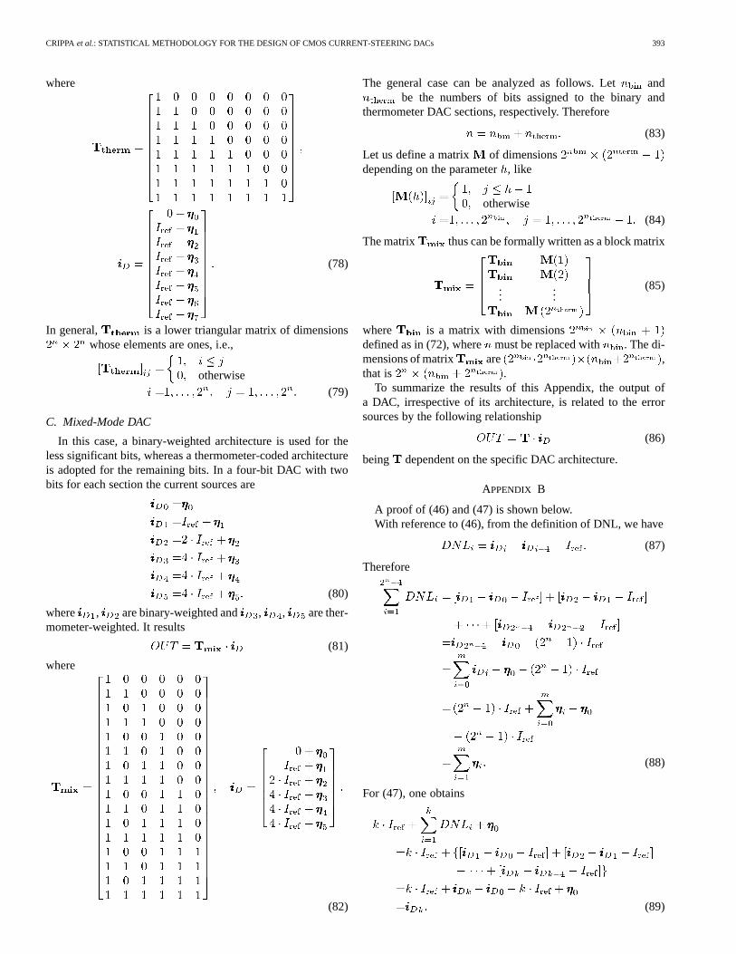
where
(78)
In general, is a lower triangular matrix of dimensionswhose elements are ones, i.e.,
otherwise(79)
C. Mixed-Mode DAC
In this case, a binary-weighted architecture is used for theless significant bits, whereas a thermometer-coded architectureis adopted for the remaining bits. In a four-bit DAC with twobits for each section the current sources are
(80)
where , are binary-weighted and , , are ther-mometer-weighted. It results
(81)
where
(82)
The general case can be analyzed as follows. Let andbe the numbers of bits assigned to the binary and
thermometer DAC sections, respectively. Therefore
(83)
Let us define a matrix of dimensionsdepending on the parameter, like
otherwise(84)
The matrix thus can be formally written as a block matrix
......
(85)
where is a matrix with dimensionsdefined as in (72), where must be replaced with . The di-mensions of matrix are ,that is .
To summarize the results of this Appendix, the output ofa DAC, irrespective of its architecture, is related to the errorsources by the following relationship
(86)
being dependent on the specific DAC architecture.
APPENDIX B
A proof of (46) and (47) is shown below.With reference to (46), from the definition of DNL, we have
(87)
Therefore
(88)
For (47), one obtains
(89)
394 IEEE TRANSACTIONS ON COMPUTER-AIDED DESIGN OF INTEGRATED CIRCUITS AND SYSTEMS, VOL. 21, NO. 4, APRIL 2002
REFERENCES
[1] B. Razavi,Principles of Data Conversion System Design. Piscataway,NJ: IEEE Press, 1995.
[2] Y. Nakamura, T. Miki, A. Maeda, H. Kondoh, and N. Yazawa, “A 10-b70-MS/s CMOS D/A converter,”IEEE J. Solid-State Circuits, vol. 26,pp. 637–642, Apr. 1991.
[3] C. A. A. Bastiaansen, D. W. J. Groeneveld, H. J. Schouwenaars, andH. A. H. Termer, “A 10-b 40 MHz 0.8-�m CMOS current-output D/Aconverter,”IEEE J. Solid-State Circuits, vol. 26, pp. 917–921, July 1991.
[4] J. Bastos, M. Steyaert, and W. Sansen, “A high yield 12-bit 250-MS/sCMOS A/D converter,” inProc. IEEE Custom Integrated Circuits Conf.,San Diego, CA, May 1996, pp. 431–434.
[5] C.-H. Lin and K. Bult, “A 10-b, 500-Msample/s CMOS DAC in 0.6mm ,” IEEE J. Solid-State Circuits, vol. 33, pp. 1948–1958, Dec. 1998.
[6] G. A. M. Van der Plas, J. Vandenbussche, W. Sansen, M. S. J. Steyaert,and G. G. E. Gielen, “A 14-bit intrinsic accuracyQ random walkCMOS DAC,” IEEE J. Solid-State Circuits, vol. 34, pp. 1708–1718,Dec. 1999.
[7] A. Van den Bosch, M. Steyaert, and W. Sansen, “An accurate statisticalyield model for CMOS current-steering D/A converters,” inProc. IEEEInt. Symp. Circuits and Systems, vol. 4, Geneva, Switzerland, May 2000,pp. 105–108.
[8] G. Van der Plas, J. Vandenbussche, W. Daems, A. Van den Bosch, G.Gielen, M. Steyaert, and W. Sansen, “Systematic design of a 14-bit150-MS/s CMOS current-steering D/A converter,” inProc. 37th DesignAutomation Conf., Los Angeles, CA, June 2000, pp. 452–457.
[9] C. S. G. Conroy, W. A. Lane, and M. A. Moran, “Statistical design tech-niques for D/A converters,”IEEE J. Solid-State Circuits, vol. 24, pp.1118–1128, Aug. 1989.
[10] E. Liu and A. Sangiovanni-Vincentelli, “Verification of Nyquist dataconverters using behavioral simulation,”IEEE Trans. Computer-AidedDesign, vol. 14, pp. 493–502, Apr. 1995.
[11] J. J. Wikner and N. Tan, “Modeling of CMOS digital-to-analog con-verters for telecommunication,” inProc. IEEE Int. Symp. Circuits andSystems, vol. 1, Monterey, CA, June 1998, pp. 25–28.
[12] T. B. Tarim, H. H. Kuntman, and M. Ismail, “Statistical design of a D/Aconverter based on the current division technique,” inProc. IEEE Int.Conf. Electronic Circuits and Systems, vol. 2, Lisbon, Portugal, Sept.1998, pp. 295–298.
[13] J. J. Wikner and N. Tan, “Influence of circuit imperfections on the per-formance of DAC’s,”Analog Integrated Circuit and Signal Processing,vol. 18, no. 1, pp. 7–20, Jan. 1999.
[14] G. Van der Plas, J. Vandenbussche, W. Verhaegen, G. Gielen, and W.Sansen, “Statistical behavioral modeling for A/D converters,” inProc.IEEE Int. Conf. Electronic Circuits and Systems, vol. 3, Paphos, Cyprus,Sept. 1999, pp. 1713–1716.
[15] K. R. Lakshmikumar, R. A. Hadaway, and M. A. Copeland, “Charac-terization and modeling of mismatch in MOS transistors for precisionanalog design,”IEEE J. Solid-State Circuits, vol. SC-21, pp. 1057–1066,Dec. 1986.
[16] M. J. M. Pelgrom, A. C. J. Duinmaijer, and A. P. G. Welbers, “Matchingproperties of MOS transistors,”IEEE J. Solid-State Circuits, vol. 24, pp.1433–1439, Oct. 1989.
[17] C. Michael and M. Ismail, “Statistical modeling of device mismatch foranalog MOS integrated circuits,”IEEE J. Solid-State Circuits, vol. 27,pp. 154–166, Feb. 1992.
[18] C. Guardiani, A. Tomasini, J. Benkoski, M. Quarantelli, and P. Gubian,“Applying a submicron mismatch model to pratical IC design,” inProc.IEEE Custom Integrated Circuits Conf., San Diego, CA, May 1994, pp.297–300.
[19] M. Conti, P. Crippa, S. Orcioni, and C. Turchetti, “Parametric yield for-mulation of MOS IC’s affected by mismatch effect,”IEEE Trans. Com-puter-Aided Design, vol. 18, pp. 582–596, May 1999.
[20] C. Michael and M. Ismail,Statistical Modeling for Computer-Aided De-sign of MOS VLSI Circuits. Boston, MA: Kluwer Academic, 1993.
[21] C. Michael, C. Abel, and C. S. Teng, “A flexible statistical model forCAD of submicrometer analog CMOS integrated circuits,” inDig. Tech.Papers IEEE/ACM Int. Conf. Computer-Aided Design, Santa Clara, CA,Nov. 1993, pp. 330–333.
[22] M. Conti, P. Crippa, S. Orcioni, and C. Turchetti, “Statistical modelingof MOS transistor mismatch based on the parameters’ autocorrelationfunction,” in Proc. IEEE Int. Symp. Circuits and Systems, vol. 6, Or-lando, FL, June 1999, pp. 222–225.
[23] B. D. Ripley,Spatial Statistics. New York: Wiley, 1981.[24] J. L. Doob,Stochastic Processes. New York: Wiley, 1990.[25] J. Oehm, U. Grünebaum, and K. Schumacher, “Overcoming insuffi-
ciences of first order mismatch modeling,” inProc. 24th Eur. Solid-StateCircuits Conf., The Hague, The Netherlands, Sept. 1998, pp. 508–511.
[26] U. Grünebaum, J. Oehm, and K. Schumacher, “Mismatch modeling andsimulation—A comprehensive approach,”Analog Integrated Circuitsand Signal Processing, vol. 29, no. 3, pp. 165–171, Dec. 2001.
[27] P. Crippa, M. Conti, and C. Turchetti, “A statistical methodology for thedesign of high-performance current steering DAC’s,” inProc. IEEE Int.Symp. Circuits and Systems, vol. 5, Sydney, Australia, May 2001, pp.311–314.
[28] E. S. Karhunen, F. V. Fernández, and A. Rodríguez-Vázquez, “Mis-match distance term compensation in centroid configurations withnonzero-area devices,” inProc. IEEE Int. Symp. Circuits and Systems,vol. 3, Hong Kong, May 1997, pp. 1644–1647.
[29] M. Mojal, “Multi bit DAC with corrective gate to drain voltage for op-timum matching under gradient temperature effects,” inProc. IEEE Int.Conf. Electronic Circuits and Systems, vol. 1, Lisbon, Portugal, Sept.1998, pp. 139–142.
Paolo Crippa received the Laurea degree (summacum laude) in electronics engineering in 1994 and thePh.D. degree in electronics engineering in 1999 fromthe University of Ancona, Italy.
From 1994 to 1999, he was a Research Fellowwith the Department of Electronics, Universityof Ancona. Since 1999, he has been an AssistantProfessor with the same Department. His researchinterests include statistical device modeling andsimulation, mismatch analysis of integrated circuitsfor parametric yield optimization, mixed-signal
circuit design, and neural networks.
Claudio Turchetti received the Laurea degreein electronics engineering from the University ofAncona, Italy, in 1979.
He joined the Department of Electronics, Univer-sity of Ancona in 1980, where he is currently a fullProfessor of Applied Electronics and Integrated Cir-cuits Design. He has been active in the areas of de-vice modeling, circuits simulation at the device level,and design of integrated circuits. His current researchinterests are also in analog neural networks and sta-tistical analysis of integrated circuits for parametric
yield optimization.
Massimo Contigraduated with the Laurea degree inelectronics engineering from the University of An-cona, Italy, in 1987.
After a three-year fellowship, he joined the Depart-ment of Electronics, University of Ancona, where heis presently an Associate Professor of Electronic De-vices. His research interests are in the fields of de-vice modeling, statistical circuit simulation, design ofmixed-signal integrated circuits, system level designof ICs.