Modulation techniques comparison for three levels VSI converters
Upload
independentCategory
view
3download
0
Matrix Converters : A Technology Review.
P. W. Wheeler, J. Rodriguez, J. Clare, L. Empringham and A. Weinstein
I. INTRODUCTION
Among the most desirable features in power frequency changers are :
i. Simple and compact power circuit.
ii. Generation of load voltage with arbitrary amplitude and frequency.
iii. Sinusoidal input and output currents.
iv. Operation with unity power factor for any load.
v. Regeneration capability.
These ideal characteristics can be fulfilled by Matrix Converters and this is the reason for the
tremendous interest in the topology.
The Matrix Converter is a forced commutated converter which uses an array of controlled bi-
directional switches as the main power elements to create a variable output voltage system with
unrestricted frequency. It does not have any dc-link circuit and does not need any large energy
storage elements.
The key element in a Matrix Converter is the fully controlled four-quadrant bidirectional switch,
which allows high frequency operation. The early work dedicated to unrestricted frequency
changers used thyristors with external forced commutation circuits to implement the bi-
directional controlled switch [1], [2], [3], [4]. With this solution the power circuit was bulky and
the performance was poor.
The introduction of power transistors for implementing the bi-directional switches made the
Matrix Converter topology more attractive [5], [6], [7], [8], [9]. However, the real development
of Matrix Converters starts with the work of Venturini and Alesina published in 1980 [10], [11].
They presented the power circuit of the converter as a matrix of bi-directional power switches
and they introduced the name “Matrix Converter.” One of their main contributions is the
development of a rigorous mathematical analysis to describe the low-frequency behavior of the
converter, introducing the “low frequency modulation matrix” concept. In their modulation
method, also known as the direct transfer function approach, the output voltages are obtained by
the multiplication of the modulation (also called transfer) matrix with the input voltages.
A conceptually different control technique based on the “fictitious dc link” idea was introduced
by Rodriguez in 1983 [12]. In this method the switching is arranged so that each output line is
switched between the most positive and most negative input lines using a PWM technique, as
conventionally used in standard voltage source inverters. This concept is also known as the
“indirect transfer function” approach [15]. In 1985/86, Ziogas et al published 2 papers [13], [40]
which expanded on the fictitious dc link idea of Rodriguez and provided a rigorous mathematical
explanation. In 1983 Braun [16] and in 1985 Kastner and Rodriguez [18] introduced the use of
space vectors in the analysis and control of Matrix Converters. In 1989, Huber et al published the
first of a series of papers [14], [41-45] in which the principles of Space Vector Modulation
(SPVM) were applied to the Matrix Converter modulation problem [17].
The modulation methods based on the Venturini approach, are known as “direct methods”, while
those based on the fictitious dc link are known as “indirect methods.”
It was experimentally confirmed by Kastner and Rodriguez in 1985 [18] and Neft and Schauder
in 1992 [19] that a Matrix Converter with only 9 switches can be effectively used in the vector
control of an induction motor with high quality input and output currents. However, the
simultaneous commutation of controlled bi-directional switches used in Matrix Converters is
very difficult to achieve without generating overcurrent or overvoltage spikes that can destroy the
power semiconductors. This fact limited the practical implementation and negatively affected the
interest in Matrix Converters. Fortunately, this major problem has been solved with the
development of several multistep commutation strategies that allow safe operation of the
switches. In 1989 Burany [36] introduced the later named “semi-soft current commutation”
technique. Other interesting commutation strategies were introduced by Ziegler et al [22], [37]
and Clare and Wheeler in 1998 [21],[38][39].
Today the research is mainly focused on operational and technological aspects: reliable
implementation of commutation strategies [20]; protection issues [23], [24]; implementation of
bidirectional switches and packaging [25], [26]; operation under abnormal conditions; ride-
through capability [28] and input filter design [29], [30].
The purpose of this paper is to give a review of key aspects concerning Matrix Converter
operation and to establish the state of the art of this technology. It begins by studying the
topology of the Matrix Converter, the main control techniques, the practical implementation of
bi-directional switches and commutation strategies. Finally, some practical issues and challenges
for the future are discussed.
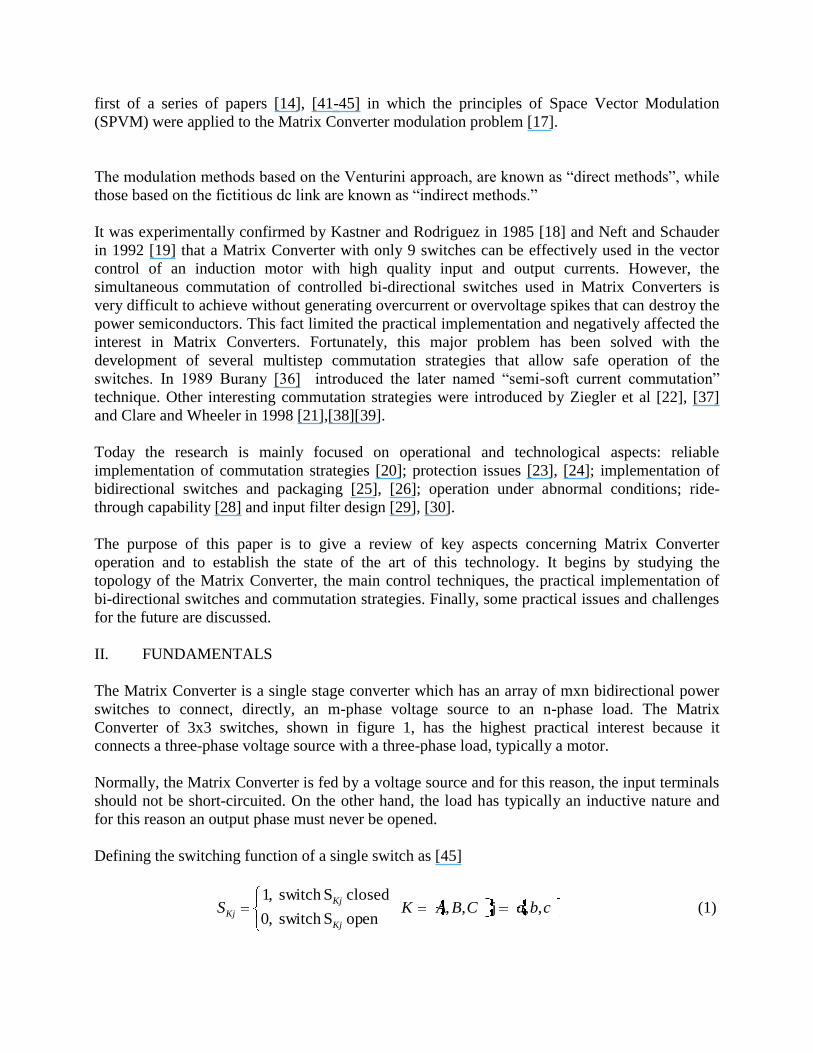
II. FUNDAMENTALS
The Matrix Converter is a single stage converter which has an array of mxn bidirectional power
switches to connect, directly, an m-phase voltage source to an n-phase load. The Matrix
Converter of 3x3 switches, shown in figure 1, has the highest practical interest because it
connects a three-phase voltage source with a three-phase load, typically a motor.
Normally, the Matrix Converter is fed by a voltage source and for this reason, the input terminals
should not be short-circuited. On the other hand, the load has typically an inductive nature and
for this reason an output phase must never be opened.
Defining the switching function of a single switch as [45]
cbaCBAKSKj
Kj
Kj ,,j ,, open Sswitch ,0
closed Sswitch ,1 (1)
The constraints discussed above can be expressed by
cbaSSS CjBjAj ,,j 1 (2)
With these restrictions, the 3x3 Matrix Converter has 27 possible switching states [45].
0
vC
vB
vA
iA
iB
iC
A
B
C
ia
ib
ic
SAa
va
vb
vc
Fig. 1. Simplified circuit of a 3x3 Matrix Converter.
The load and source voltages are referenced to the supply neutral, „0‟ in figure 1, and can be
expressed as vectors defined by:
)(
)(
)(
;
)(
)(
)(
tv
tv
tv
tv
tv
tv
C
B
A
c
b
a
io vv (3)
The relationship between load and input voltages can be expressed as:
i0 T·vv
)(
)(
)(
)()()(
)()()(
)()()(
)(
)(
)(
tv
tv
tv
tStStS
tStStS
tStStS
tv
tv
tv
C
B
A
CcBcAc
CbBbAb
CaBaAa
c
b
a
(4)
Where T is the instantaneous transfer matrix.
In the same form, the following relationships are valid for the input and output currents:
)(
)(
)(
;
)(
)(
)(
ti
ti
ti
ti
ti
ti
C
B
A
c
b
a
oi ii (5)
oi iTi ·T (6)
Where TT is the transpose matrix of T.
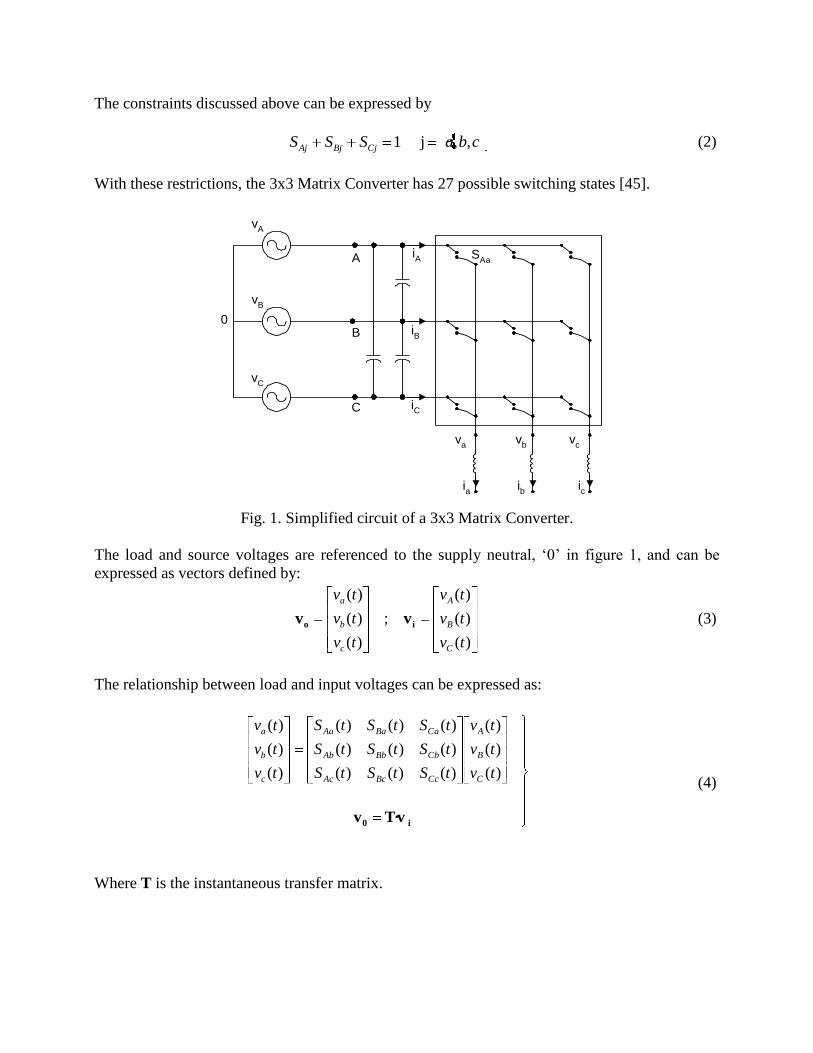
Equations (4) and (6) give the instantaneous relationships between input and output quantities. To
derive modulation rules, it is also necessary to consider the switching pattern that is employed.
This typically follows a form similar to that shown in figure 2.
Tseq
(sequence time)
SAb=1
SBa =1 SCa=1SAa=1
SBb=1 SCb=1
SAc=1 SBc=1 SCc=1
tAa tBa tCa
tAb tBb tCb
tAc tBc tCc
Outputphase a
Outputphase b
Outputphase c
Repeats
Fig. 2. General form of switching pattern.
By considering that the bidirectional power switches work with high switching frequency, a low
frequency output voltage of variable amplitude and frequency can be generated by modulating
the duty cycle of the switches using their respective switching functions.
Let mKj (t) be the duty cycle of switch SKj, defined as mKj(t)=tKj/Tseq, which can have the
following values
cbaCBAmKj ,,j ,,K 10 (7)
The low-frequency transfer matrix is defined by
)()()(
)()()(
)()()(
)(
tmtmtm
tmtmtm
tmtmtm
t
CcBcAc
CbBbAb
CaBaAa
M (8)
The low-frequency component of the output phase voltage is given by
)()()( ttt io ·vMv (9)
The low-frequency component of the input current is
oi iMi ·)( Tt (10)
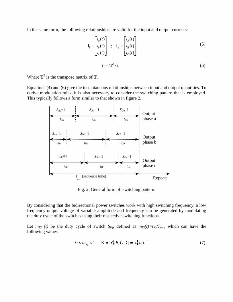
Figure 3 shows simulated waveforms generated by a Matrix Converter.
0 0.005 0.01 0.015 0.02 0.025 0.03 0.035 0.04-400
-300
-200
-100
0
100
200
300
400a)
Time [s]
[V]
0 0.005 0.01 0.015 0.02 0.025 0.03 0.035 0.04-20
-15
-10
-5
0
5
10
15
20b)
Time [s]
[A]
Fig. 3 : Typical waveforms : a) Phase output voltage ; b) Load current
III. THE BIDIRECTIONAL SWITCH
The Matrix Converter requires a bi-directional switch capable of blocking voltage and conducting
current in both directions. Unfortunately there are no such devices currently available, so
discrete devices need to be used to construct suitable switch cells.
A Realization with discrete semiconductors
The diode bridge bi-directional switch cell arrangement consists of an IGBT at the center of a
single-phase diode bridge [19] arrangement as shown in figure 4. The main advantage is that
both current directions are carried by the same switching device, therefore only one gate driver is
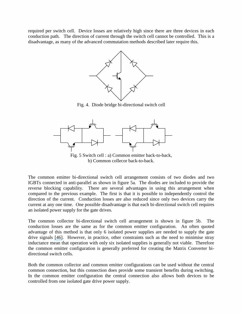
required per switch cell. Device losses are relatively high since there are three devices in each
conduction path. The direction of current through the switch cell cannot be controlled. This is a
disadvantage, as many of the advanced commutation methods described later require this.
Fig. 4. Diode bridge bi-directional switch cell
Fig. 5 Switch cell : a) Common emitter back-to-back,
b) Common collecor back-to-back.
The common emitter bi-directional switch cell arrangement consists of two diodes and two
IGBTs connected in anti-parallel as shown in figure 5a. The diodes are included to provide the
reverse blocking capability. There are several advantages in using this arrangement when
compared to the previous example. The first is that it is possible to independently control the
direction of the current. Conduction losses are also reduced since only two devices carry the
current at any one time. One possible disadvantage is that each bi-directional switch cell requires
an isolated power supply for the gate drives.
The common collector bi-directional switch cell arrangement is shown in figure 5b. The
conduction losses are the same as for the common emitter configuration. An often quoted
advantage of this method is that only 6 isolated power supplies are needed to supply the gate
drive signals [46]. However, in practice, other constraints such as the need to minimise stray
inductance mean that operation with only six isolated supplies is generally not viable. Therefore
the common emitter configuration is generally preferred for creating the Matrix Converter bi-
directional switch cells.
Both the common collector and common emitter configurations can be used without the central
common connection, but this connection does provide some transient benefits during switching.
In the common emitter configuration the central connection also allows both devices to be
controlled from one isolated gate drive power supply.
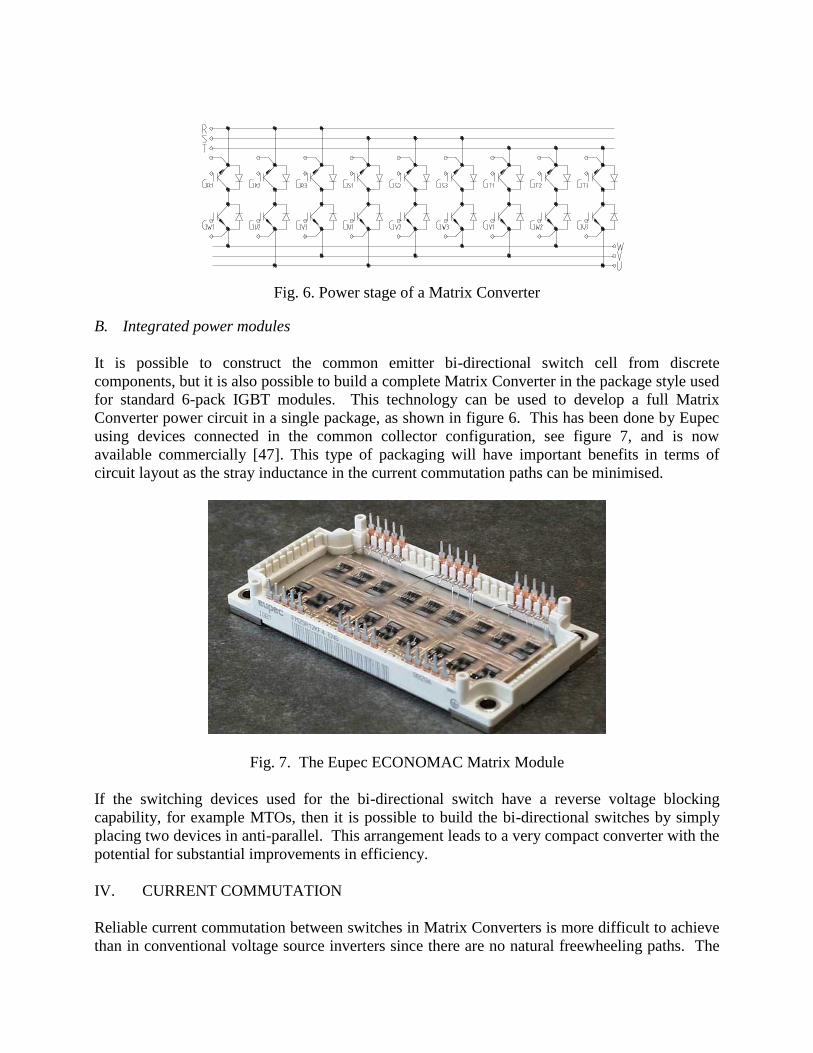
Fig. 6. Power stage of a Matrix Converter
B. Integrated power modules
It is possible to construct the common emitter bi-directional switch cell from discrete
components, but it is also possible to build a complete Matrix Converter in the package style used
for standard 6-pack IGBT modules. This technology can be used to develop a full Matrix
Converter power circuit in a single package, as shown in figure 6. This has been done by Eupec
using devices connected in the common collector configuration, see figure 7, and is now
available commercially [47]. This type of packaging will have important benefits in terms of
circuit layout as the stray inductance in the current commutation paths can be minimised.
Fig. 7. The Eupec ECONOMAC Matrix Module
If the switching devices used for the bi-directional switch have a reverse voltage blocking
capability, for example MTOs, then it is possible to build the bi-directional switches by simply
placing two devices in anti-parallel. This arrangement leads to a very compact converter with the
potential for substantial improvements in efficiency.
IV. CURRENT COMMUTATION
Reliable current commutation between switches in Matrix Converters is more difficult to achieve
than in conventional voltage source inverters since there are no natural freewheeling paths. The
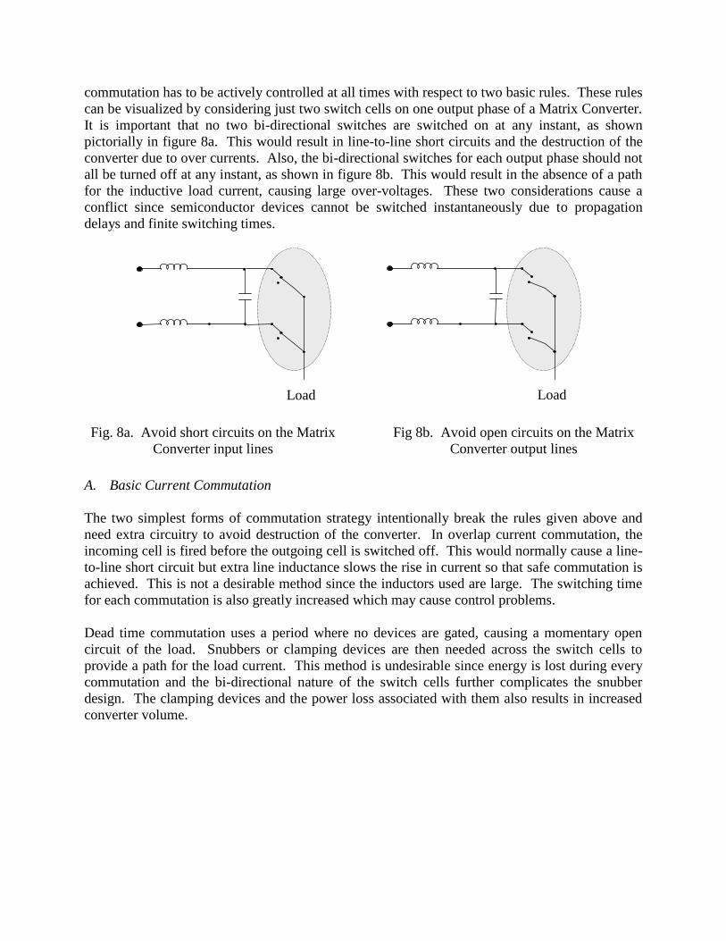
commutation has to be actively controlled at all times with respect to two basic rules. These rules
can be visualized by considering just two switch cells on one output phase of a Matrix Converter.
It is important that no two bi-directional switches are switched on at any instant, as shown
pictorially in figure 8a. This would result in line-to-line short circuits and the destruction of the
converter due to over currents. Also, the bi-directional switches for each output phase should not
all be turned off at any instant, as shown in figure 8b. This would result in the absence of a path
for the inductive load current, causing large over-voltages. These two considerations cause a
conflict since semiconductor devices cannot be switched instantaneously due to propagation
delays and finite switching times.
Fig. 8a. Avoid short circuits on the Matrix
Converter input lines
Fig 8b. Avoid open circuits on the Matrix
Converter output lines
A. Basic Current Commutation
The two simplest forms of commutation strategy intentionally break the rules given above and
need extra circuitry to avoid destruction of the converter. In overlap current commutation, the
incoming cell is fired before the outgoing cell is switched off. This would normally cause a line-
to-line short circuit but extra line inductance slows the rise in current so that safe commutation is
achieved. This is not a desirable method since the inductors used are large. The switching time
for each commutation is also greatly increased which may cause control problems.
Dead time commutation uses a period where no devices are gated, causing a momentary open
circuit of the load. Snubbers or clamping devices are then needed across the switch cells to
provide a path for the load current. This method is undesirable since energy is lost during every
commutation and the bi-directional nature of the switch cells further complicates the snubber
design. The clamping devices and the power loss associated with them also results in increased
converter volume.
Load Load
SAa1
SAa2
SBa1
SBa2
RL LOAD
IL
VA
VB
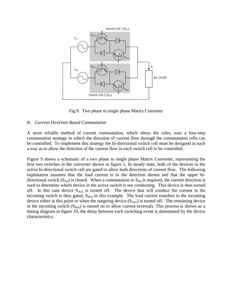
Switch Cell 1 (SAa)
Switch Cell 2 (SBa)
Fig 9. Two phase to single phase Matrix Converter
B. Current Direction Based Commutation
A more reliable method of current commutation, which obeys the rules, uses a four-step
commutation strategy in which the direction of current flow through the commutation cells can
be controlled. To implement this strategy the bi-directional switch cell must be designed in such
a way as to allow the direction of the current flow in each switch cell to be controlled.
Figure 9 shows a schematic of a two phase to single phase Matrix Converter, representing the
first two switches in the converter shown in figure 1. In steady state, both of the devices in the
active bi-directional switch cell are gated to allow both directions of current flow. The following
explanation assumes that the load current is in the direction shown and that the upper bi-
directional switch (SAa) is closed. When a commutation to SBa is required, the current direction is
used to determine which device in the active switch is not conducting. This device is then turned
off. In this case device SAa2 is turned off. The device that will conduct the current in the
incoming switch is then gated, SBa1 in this example. The load current transfers to the incoming
device either at this point or when the outgoing device (SAa1) is turned off. The remaining device
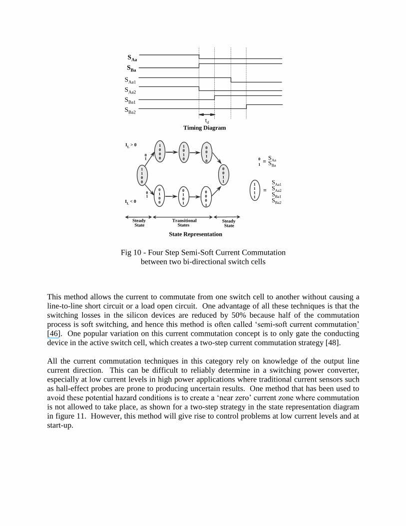
in the incoming switch (SBa2) is turned on to allow current reversals. This process is shown as a
timing diagram in figure 10, the delay between each switching event is determined by the device
characteristics.
td
SAa1
SAa2
SBa1
SBa2
SAa
SBa
Timing Diagram
State Representation
IL > 0
IL < 0
TransitionalStates
SteadyState
SteadyState
1000
1010
001
0
01
0100
0101
000
1
01
1100
0011
1111
=0
1
SAaSBa
=
SAa1SAa2SBa1SBa2
Fig 10 - Four Step Semi-Soft Current Commutation
between two bi-directional switch cells
This method allows the current to commutate from one switch cell to another without causing a
line-to-line short circuit or a load open circuit. One advantage of all these techniques is that the
switching losses in the silicon devices are reduced by 50% because half of the commutation
process is soft switching, and hence this method is often called „semi-soft current commutation‟
[46]. One popular variation on this current commutation concept is to only gate the conducting
device in the active switch cell, which creates a two-step current commutation strategy [48].
All the current commutation techniques in this category rely on knowledge of the output line
current direction. This can be difficult to reliably determine in a switching power converter,
especially at low current levels in high power applications where traditional current sensors such
as hall-effect probes are prone to producing uncertain results. One method that has been used to
avoid these potential hazard conditions is to create a „near zero‟ current zone where commutation
is not allowed to take place, as shown for a two-step strategy in the state representation diagram
in figure 11. However, this method will give rise to control problems at low current levels and at
start-up.
t d
S Aa1
S Aa2
S Ba1
S Ba2
S Aa
S Ba
Timing Diagram
State Representation
IL: > IZ
IL < - IZ
Transitional States
Steady State
Steady State
1 0 0 0
1 0 1 0
0 0 1
0
0 1
0 1 0 0
0 1 0 1
0 0 0
1 0 1
1 1 0 0
0 0 1 1
1 1 1 1
= 0
1
S Aa S Ba
=
S Aa1 S Aa2 S Ba1 S Ba2
- IZ >IL< IZ
-ΔIZ
ΔIZ
IL >ΔIZ
Time [secs]
IL<-ΔIZ
IL [Amps]
Fig. 11 - Two Step Semi-Soft Current Commutation
between two bi-directional switch cells
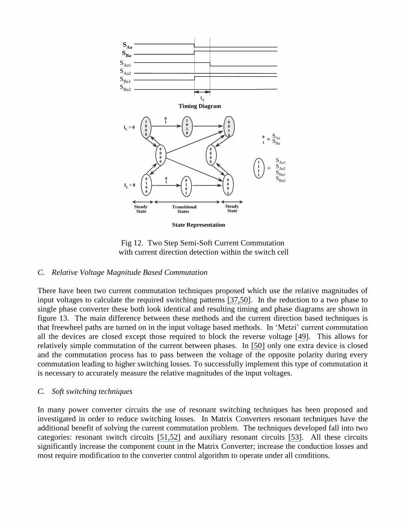
To avoid these current measurement problems a technique for using the voltage across the bi-
directional switch to determine the current direction has been developed. This method allows very
accurate current direction detection with no external sensors. Because of the accuracy available using
this method, a two-step commutation strategy can be employed with deadtimes when the current
changes direction, as shown in figure 12. This technique has been coupled with the addition of
intelligence at the gate drive level to allow each gate drive to independently control the current
commutation [21].
State Representation
IL
> 0
IL
< 0
TransitionalStates
SteadyState
SteadyState
1000
1010
001
0
01
0100
0101
000
1
01
0000
0000 1
111
=0
1
SAaSBa
=
SAa1SAa2SBa1SBa2
td
SAa1
SAa2
SBa1
SBa2
SAa
SBa
Timing Diagram
Fig 12. Two Step Semi-Soft Current Commutation
with current direction detection within the switch cell
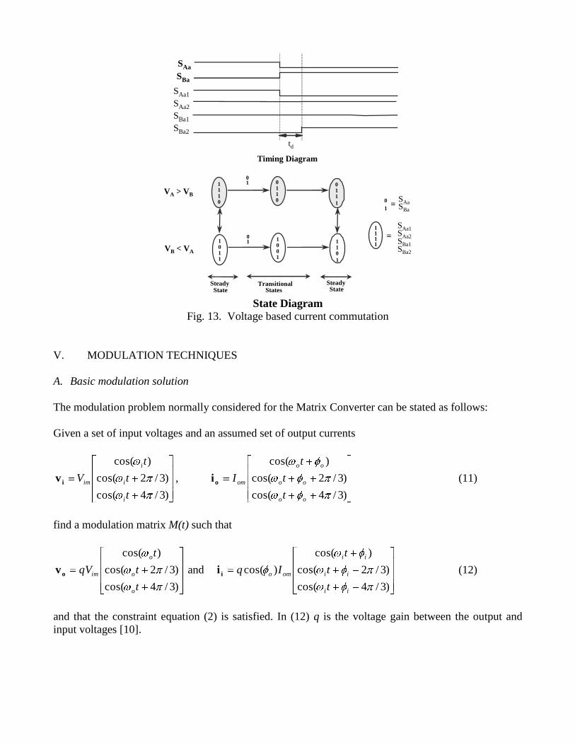
C. Relative Voltage Magnitude Based Commutation
There have been two current commutation techniques proposed which use the relative magnitudes of
input voltages to calculate the required switching patterns [37,50]. In the reduction to a two phase to
single phase converter these both look identical and resulting timing and phase diagrams are shown in
figure 13. The main difference between these methods and the current direction based techniques is
that freewheel paths are turned on in the input voltage based methods. In „Metzi‟ current commutation
all the devices are closed except those required to block the reverse voltage [49]. This allows for
relatively simple commutation of the current between phases. In [50] only one extra device is closed
and the commutation process has to pass between the voltage of the opposite polarity during every
commutation leading to higher switching losses. To successfully implement this type of commutation it
is necessary to accurately measure the relative magnitudes of the input voltages.
C. Soft switching techniques
In many power converter circuits the use of resonant switching techniques has been proposed and
investigated in order to reduce switching losses. In Matrix Converters resonant techniques have the
additional benefit of solving the current commutation problem. The techniques developed fall into two
categories: resonant switch circuits [51,52] and auxiliary resonant circuits [53]. All these circuits
significantly increase the component count in the Matrix Converter; increase the conduction losses and
most require modification to the converter control algorithm to operate under all conditions.
VA > VB
TransitionalStates
SteadyState
SteadyState
1110
0110
011
1
01
=0
1
SAaSBa
1111
=
SAa1SAa2SBa1SBa2
VB < VA
1011
1001
110
1
01
td
SAa1
SAa2
SBa1
SBa2
SAa
SBa
Timing Diagram
State Diagram
Fig. 13. Voltage based current commutation
V. MODULATION TECHNIQUES
A. Basic modulation solution
The modulation problem normally considered for the Matrix Converter can be stated as follows:
Given a set of input voltages and an assumed set of output currents
)3/4cos(
)3/2cos(
)cos(
t
t
t
V
i
i
i
imiv ,
)3/4cos(
)3/2cos(
)cos(
oo
oo
oo
om
t
t
t
Ioi (11)
find a modulation matrix M(t) such that
)3/4cos(
)3/2cos(
)cos(
t
t
t
qV
o
o
o
imov and
)3/4cos(
)3/2cos(
)cos(
)cos(
ii
ii
ii
omo
t
t
t
Iqii (12)
and that the constraint equation (2) is satisfied. In (12) q is the voltage gain between the output and
input voltages [10].
There are 2 basic solutions [10,11,54]:
)(with
)cos(21)3/4cos(21)3/2cos(21
)3/2cos(21)cos(21)3/4cos(21
)3/4cos(21)3/2cos(21)cos(21
3
1
iom
mmm
mmm
mmm
tqtqtq
tqtqtq
tqtqtq
M1 (13)
and
)(with
)3/2cos(21)cos(21)3/4cos(21
)cos(21)3/4cos(21)3/2cos(21
)3/4cos(21)3/2cos(21)cos(21
3
1
iom
mmm
mmm
mmm
tqtqtq
tqtqtq
tqtqtq
M2 (14)
The solution in (13) yields i = o giving the same phase displacement at the input and output ports
whereas the solution in (14) yields i = - o giving reversed phase displacement. Combining the two
solutions provides the means for input displacement factor control.
This basic solution represents a direct transfer function approach and is characterised by the fact that,
during each switch sequence time (Tseq), the average output voltage is equal to the demand (target)
voltage. For this to be possible it is clear that the target voltages must fit within the input voltage
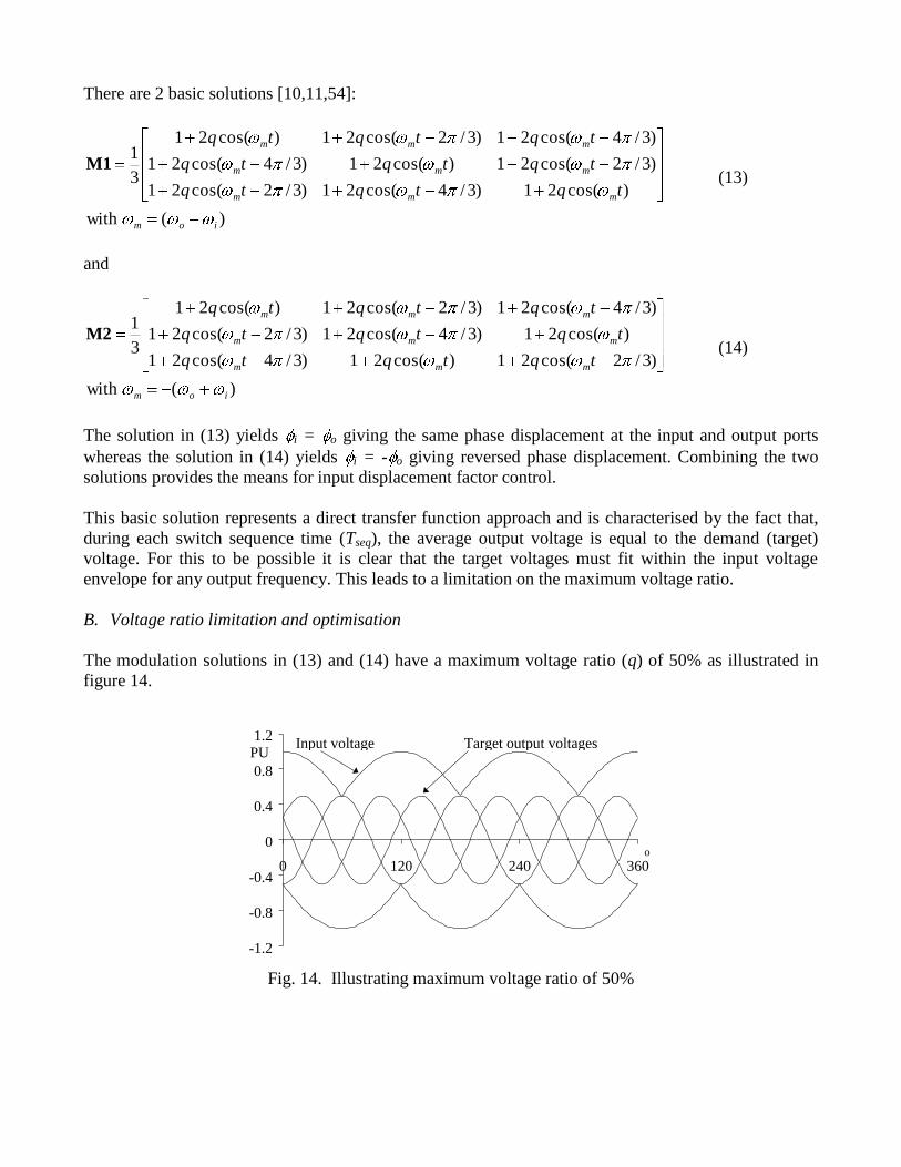
envelope for any output frequency. This leads to a limitation on the maximum voltage ratio.
B. Voltage ratio limitation and optimisation
The modulation solutions in (13) and (14) have a maximum voltage ratio (q) of 50% as illustrated in
figure 14.
-1.2
-0.8
-0.4
0
0.4
0.8
1.2
0 120 240 360
Input voltage Target output voltages PU
o
Fig. 14. Illustrating maximum voltage ratio of 50%
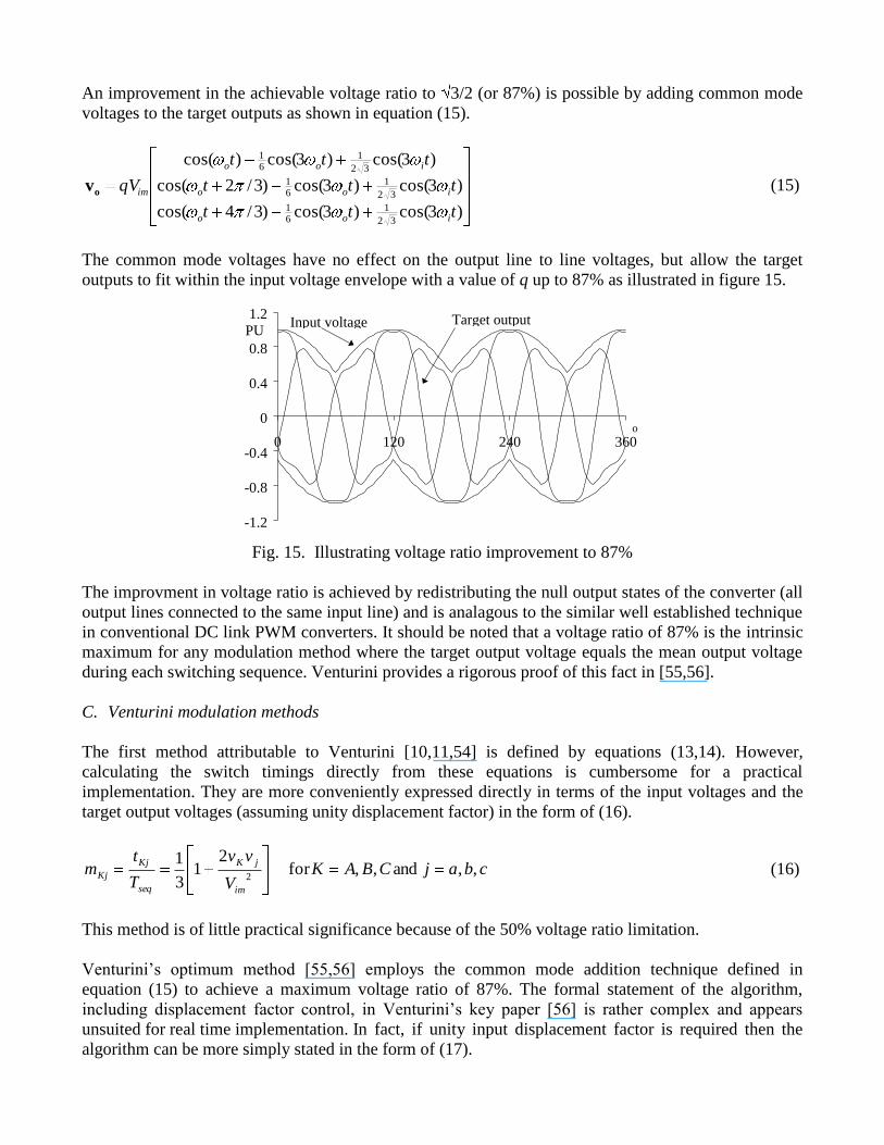
An improvement in the achievable voltage ratio to 3/2 (or 87%) is possible by adding common mode
voltages to the target outputs as shown in equation (15).
)3cos()3cos()3/4cos(
)3cos()3cos()3/2cos(
)3cos()3cos()cos(
32
161
32
161
32
161
ttt
ttt
ttt
qV
ioo
ioo
ioo
imov (15)
The common mode voltages have no effect on the output line to line voltages, but allow the target
outputs to fit within the input voltage envelope with a value of q up to 87% as illustrated in figure 15.
-1.2
-0.8
-0.4
0
0.4
0.8
1.2
0 120 240 360
Input voltage Target output PU
o
Fig. 15. Illustrating voltage ratio improvement to 87%
The improvment in voltage ratio is achieved by redistributing the null output states of the converter (all
output lines connected to the same input line) and is analagous to the similar well established technique
in conventional DC link PWM converters. It should be noted that a voltage ratio of 87% is the intrinsic
maximum for any modulation method where the target output voltage equals the mean output voltage
during each switching sequence. Venturini provides a rigorous proof of this fact in [55,56].
C. Venturini modulation methods
The first method attributable to Venturini [10,11,54] is defined by equations (13,14). However,
calculating the switch timings directly from these equations is cumbersome for a practical
implementation. They are more conveniently expressed directly in terms of the input voltages and the
target output voltages (assuming unity displacement factor) in the form of (16).
cbajCBAKV
vv
T
tm
im
jK
seq
Kj
Kj ,,and,,for2
13
12
(16)
This method is of little practical significance because of the 50% voltage ratio limitation.
Venturini‟s optimum method [55,56] employs the common mode addition technique defined in
equation (15) to achieve a maximum voltage ratio of 87%. The formal statement of the algorithm,
including displacement factor control, in Venturini‟s key paper [56] is rather complex and appears
unsuited for real time implementation. In fact, if unity input displacement factor is required then the
algorithm can be more simply stated in the form of (17).
lyrespective for
,,and,,for)3sin()sin(33
421
3
12
A,B,CK/3/3,40,2
cbajCBAKttq
V
vvm
K
iKi
im
jK
Kj (17)
Note that in (17), the target output voltages, vj, include the common mode addition defined in (15).
Equation (17) provides a basis for real-time implementation of the optimum amplitude Venturini
method which is readily handled by processors up to sequence (switching) frequencies of tens of kHz.
Input displacement factor control can be introduced by inserting a phase shift between the measured
input voltages and the voltages, vK, inserted into (17). However, like all other methods, displacement
factor control is at the expense of maximum voltage ratio.
Figure 3 shown previously illustrates typical line to supply neutral output voltage and current
waveforms generated by the Venturini method.
C. Scalar modulation methods
The “scalar” modulation method of Roy [57,58] is typical of a number of modulation methods which
have been developed where the switch actuation signals are calculated directly from measurements of
the input voltages. The motivation behind their development is usually given as the perceived
complexity of the Venturini method. The scalar method relies on measuring the instantaneous input
voltages and comparing their relative magnitudes following the algorithm below.
Rule1: Assign subscript M to the input which has a different polarity to the other two.
Rule 2: Assign subscript L to the smallest (absolute) of the other two inputs. Third input is assigned
subscript K
The modulation duty cycles are then given by:
cbajmmmV
vvvm
V
vvvm KjLjMj
im
KMj
Kj
im
LMj
Lj ,,for)(1,5.1
)(,
5.1
)(22
(18)
Again, common mode addition is used with the target output voltages, vj, to achieve 87% voltage ratio
capability.
Despite the apparent differences, this method yields virtually identical switch timings to the optimum
Venturini method. Expressed in the form of (17) the modulation duty cycles for the scalar method are
given in (19).
)3sin()sin(3
221
3
12
ttV
vvm iKi
im
jK
Kj (19)
At maximum output voltage (q = 3/2), equations (17) and (19) are identical. The only difference
between the methods is that the rightmost term addition is taken pro-rata with q in the Venturini
method and is fixed at its maximum value in the scalar method. The effect on output voltage quality is
negligible except at low switching frequencies where the Venturini method is superior.
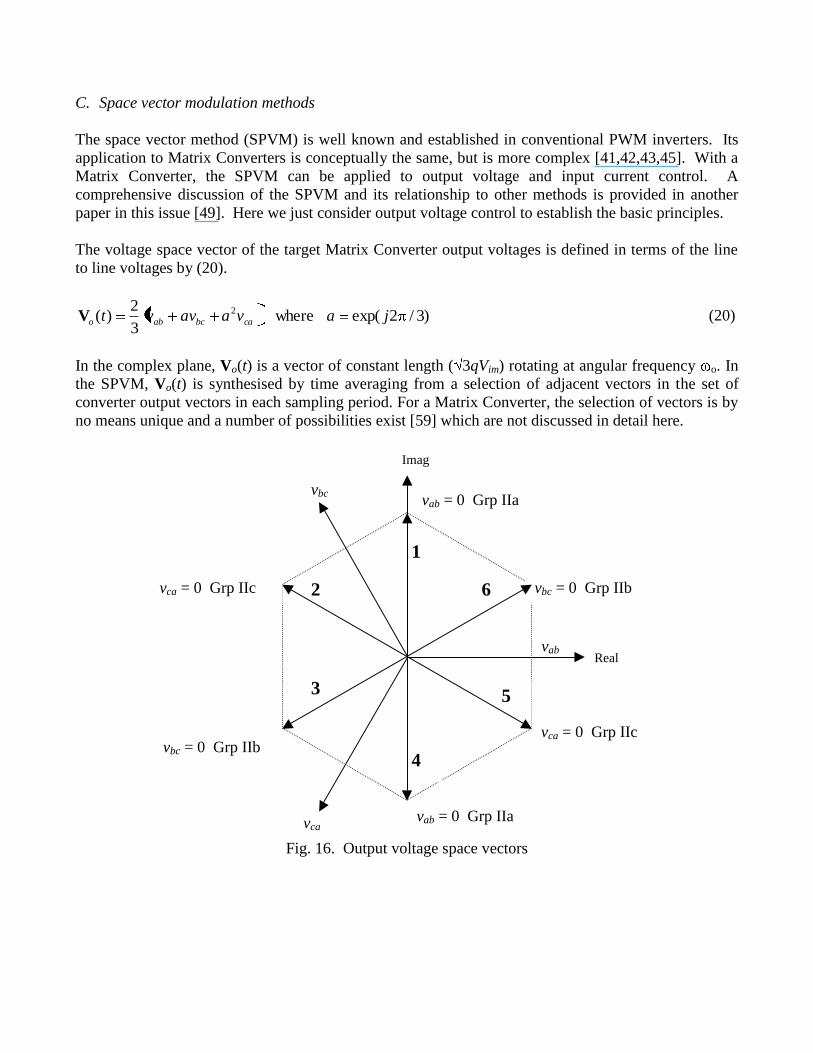
C. Space vector modulation methods
The space vector method (SPVM) is well known and established in conventional PWM inverters. Its
application to Matrix Converters is conceptually the same, but is more complex [41,42,43,45]. With a
Matrix Converter, the SPVM can be applied to output voltage and input current control. A
comprehensive discussion of the SPVM and its relationship to other methods is provided in another
paper in this issue [49]. Here we just consider output voltage control to establish the basic principles.
The voltage space vector of the target Matrix Converter output voltages is defined in terms of the line
to line voltages by (20).
)3/2exp(where3
2)( 2 javaavvt cabcaboV (20)
In the complex plane, Vo(t) is a vector of constant length ( 3qVim) rotating at angular frequency o. In
the SPVM, Vo(t) is synthesised by time averaging from a selection of adjacent vectors in the set of
converter output vectors in each sampling period. For a Matrix Converter, the selection of vectors is by
no means unique and a number of possibilities exist [59] which are not discussed in detail here.
6
5
4
3
2
1
vca
vbc
vab
vca = 0 Grp IIc
vca = 0 Grp IIc vbc = 0 Grp IIb
vab = 0 Grp IIa
vab = 0 Grp IIa
Imag
Real
vbc = 0 Grp IIb
Fig. 16. Output voltage space vectors
The twentyseven possible output vectors for a three-phase Matrix Converter can be classified into three
groups with the following characteristics:
Group I: each output line is connected to a different input line. Output space vectors are constant in
amplitude, rotating (in either direction) at the supply angular frequency.
Group II: two output lines are connected to a common input line, the remaining output line is
connected to one of the other input lines. Output space vectors have varying amplitude and fixed
direction occupying one of six positions regularly spaced 600 apart. The maximum length of these
vectors is 2/ 3Venv where Venv is the instantaneous value of the rectified input voltage envelope.
Group III: all output lines are connected to a common input line. Output space vectors have zero
amplitude (ie located at the origin).
In the SPVM, the group I vectors are not used. The desired output is synthesised from the group II
active vectors and the group III zero vectors. The hexagon of possible output vectors is shown in figure
16, where the group II vectors are further sub-divided dependent on which output line to line voltage is
zero.
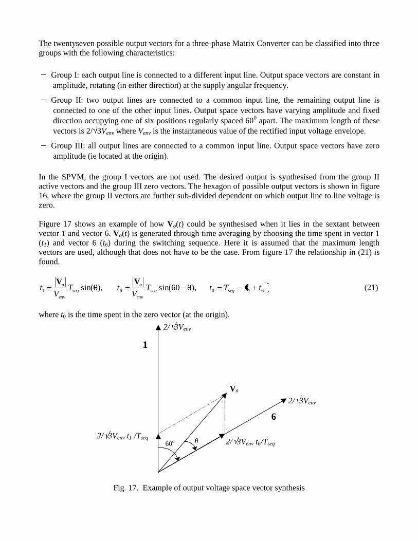
Figure 17 shows an example of how Vo(t) could be synthesised when it lies in the sextant between
vector 1 and vector 6. Vo(t) is generated through time averaging by choosing the time spent in vector 1
(t1) and vector 6 (t6) during the switching sequence. Here it is assumed that the maximum length
vectors are used, although that does not have to be the case. From figure 17 the relationship in (21) is
found.
61061 ),60sin(),sin( ttTtTV
tTV
t seqseq
env
o
seq
env
o VV (21)
where t0 is the time spent in the zero vector (at the origin).
60o
2/ 3Venv
2/ 3Venv t1 /Tseq
Vo
2/ 3Venv t6/Tseq
2/ 3Venv
6
1
Fig. 17. Example of output voltage space vector synthesis
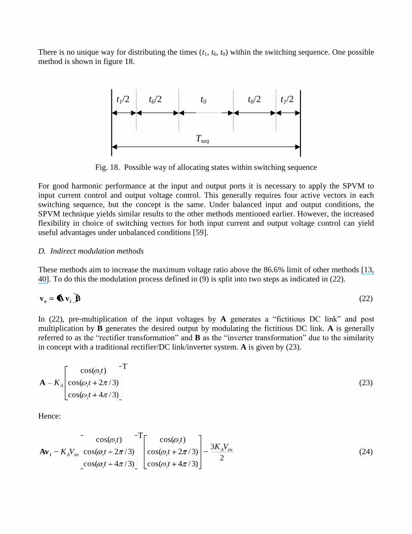
There is no unique way for distributing the times (t1, t6, t0) within the switching sequence. One possible
method is shown in figure 18.
t6/2 t6/2 t1/2t1/2
Tseq
t0
Fig. 18. Possible way of allocating states within switching sequence
For good harmonic performance at the input and output ports it is necessary to apply the SPVM to
input current control and output voltage control. This generally requires four active vectors in each
switching sequence, but the concept is the same. Under balanced input and output conditions, the
SPVM technique yields similar results to the other methods mentioned earlier. However, the increased
flexibility in choice of switching vectors for both input current and output voltage control can yield
useful advantages under unbalanced conditions [59].
D. Indirect modulation methods
These methods aim to increase the maximum voltage ratio above the 86.6% limit of other methods [13,
40]. To do this the modulation process defined in (9) is split into two steps as indicated in (22).
BvAv io (22)
In (22), pre-multiplication of the input voltages by A generates a “fictitious DC link” and post
multiplication by B generates the desired output by modulating the fictitious DC link. A is generally
referred to as the “rectifier transformation” and B as the “inverter transformation” due to the similarity
in concept with a traditional rectifier/DC link/inverter system. A is given by (23).
T
)3/4cos(
)3/2cos(
)cos(
t
t
t
K
i
i
i
AA (23)
Hence:
2
3
)3/4cos(
)3/2cos(
)cos(T
)3/4cos(
)3/2cos(
)cos(imA
i
i
i
i
i
i
imA
VK
t
t
t
t
t
t
VKiAv (24)
B is given by (25).
)3/4cos(
)3/2cos(
)cos(
t
t
t
K
o
o
o
BB (25)
Hence:
)3/4cos(
)3/2cos(
)cos(
2
3
t
t
tVKK
o
o
o
imBABAvv io (26)
The voltage ratio q = 3KAKB/2. Clearly the A and B modulation steps are not continuous in time as
shown above but must be implemented by a suitable choice of the switching states. There are many
ways of doing this which are discussed in detail in [13, 40].
To maximise the voltage ratio the step in A is implemented so that the most positive and most negative
input voltages are selected continuously. This yields KA = 2 3/ with a fictitious DC link of 3 3Vim/
(the same as a 6-pulse diode bridge with resistive load). KB represents the modulation index of a PWM
process and has the maximum value (squarewave modulation) of 2/ [13]. The overall voltage ratio q
therefore has the maximum value of 6 3/2 = 105.3%.
The voltage ratio obtainable is obviously greater than that of other methods but the improvement is
only obtained at the expense of the quality of either the input currents, the output voltages or both. For
values of q > 0.866, the mean output voltage no longer equals the target output voltage in each
switching interval. This inevitably leads to low frequency distortion in the output voltage and/or the
input current compared to other methods with q < 0.866. For q < 0.866, the indirect method yields very
similar results to the direct methods.
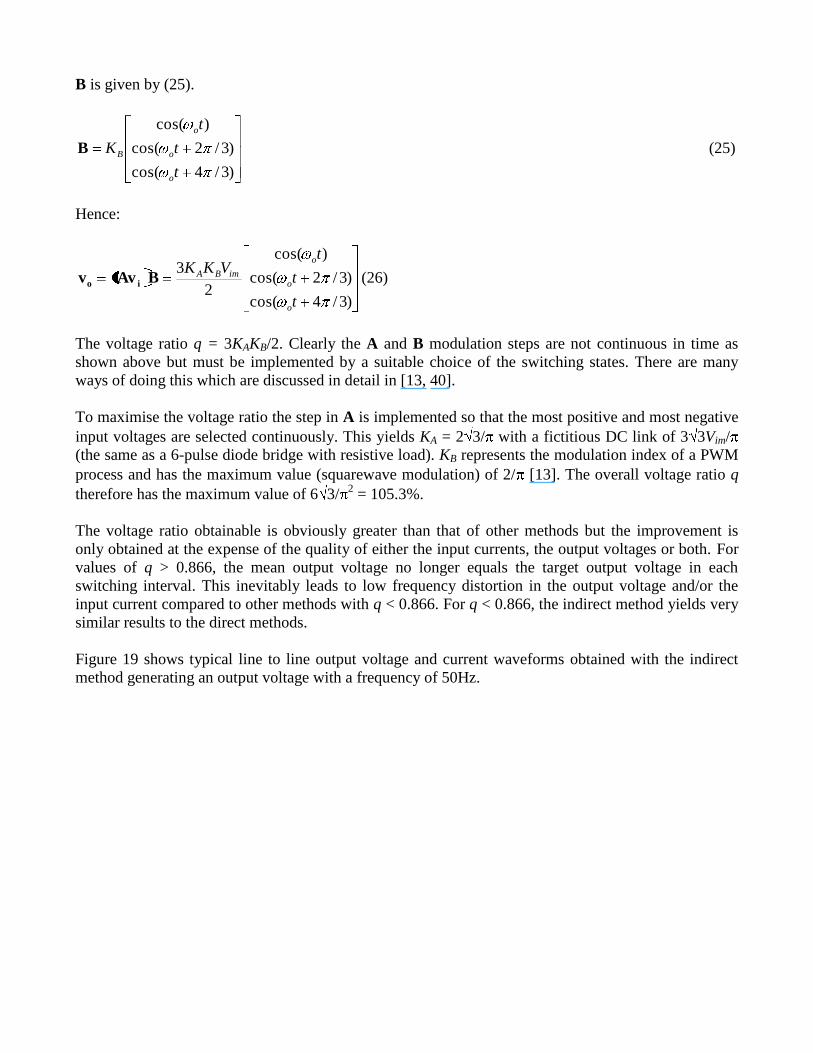
Figure 19 shows typical line to line output voltage and current waveforms obtained with the indirect
method generating an output voltage with a frequency of 50Hz.
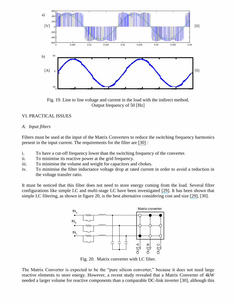
Fig. 19. Line to line voltage and current in the load with the indirect method.
Output frequency of 50 [Hz]
VI. PRACTICAL ISSUES
A. Input filters
Filters must be used at the input of the Matrix Converters to reduce the switching frequency harmonics
present in the input current. The requirements for the filter are [30] :
i. To have a cut-off frequency lower than the switching frequency of the converter.
ii. To minimise its reactive power at the grid frequency.
iii. To minimise the volume and weight for capacitors and chokes.
iv. To minimise the filter inductance voltage drop at rated current in order to avoid a reduction in
the voltage transfer ratio.
It must be noticed that this filter does not need to store energy coming from the load. Several filter
configurations like simple LC and multi-stage LC have been investigated [29]. It has been shown that
simple LC filtering, as shown in figure 20, is the best alternative considering cost and size [29], [30].
Matrix converter
OU
T A
OU
T B
OU
T C
INa
INb
INc
Fig. 20. Matrix converter with LC filter.
The Matrix Converter is expected to be the “pure silicon converter,” because it does not need large
reactive elements to store energy. However, a recent study revealed that a Matrix Converter of 4kW
needed a larger volume for reactive components than a comparable DC-link inverter [30], although this
0 0.005 0.01 0.015 0.02 0.025 0.03 0.035 0.04-600
-400
-200
0
200
400
600
0 0.005 0.01 0.015 0.02 0.025 0.03 0.035 0.04-50
0
50
a)
b)
[V]
[A]
[S]
[S]
solution had not been optimised for volume. Some preliminary research works have been reported
concerning the size reduction of the input filter [25].
Due to the LC configuration of the input filter, some problems appear during the power-up procedure
of the Matrix Converter. It is well known that an LC circuit can create overvoltage during transient
operation. The connection of damping resitors, as shown in figure 20, to reduce overvoltages is
proposed in [31]. The damping resistors are shortcircuited when the converter is running. The use of
damping resistors connected in parallel to the input reactors is proposed in [30].
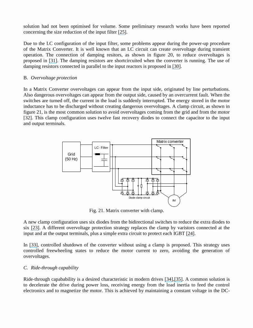
B. Overvoltage protection
In a Matrix Converter overvoltages can appear from the input side, originated by line perturbations.
Also dangerous overvoltages can appear from the output side, caused by an overcurrent fault. When the
switches are turned off, the current in the load is suddenly interrupted. The energy stored in the motor
inductance has to be discharged without creating dangerous overvoltages. A clamp circuit, as shown in
figure 21, is the most common solution to avoid overvoltages coming from the grid and from the motor
[32]. This clamp configuration uses twelve fast recovery diodes to connect the capacitor to the input
and output terminals.
Grid
(50 Hz)
LC- Filter
IM
Matrix converter
Diode clamp circuit
Fig. 21. Matrix converter with clamp.
A new clamp configuration uses six diodes from the bidirectional switches to reduce the extra diodes to
six [23]. A different overvoltage protection strategy replaces the clamp by varistors connected at the
input and at the output terminals, plus a simple extra circuit to protect each IGBT [24].
In [33], controlled shutdown of the converter without using a clamp is proposed. This strategy uses
controlled freewheeling states to reduce the motor current to zero, avoiding the generation of
overvoltages.
C. Ride-through capability
Ride-through capabability is a desired characteristic in modern drives [34],[35]. A common solution is
to decelerate the drive during power loss, receiving energy from the load inertia to feed the control
electronics and to magnetize the motor. This is achieved by maintaining a constant voltage in the DC-
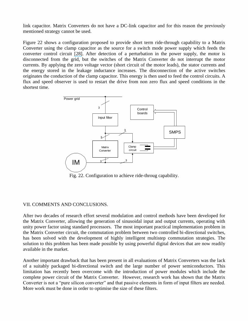
link capacitor. Matrix Converters do not have a DC-link capacitor and for this reason the previously
mentioned strategy cannot be used.
Figure 22 shows a configuration proposed to provide short term ride-through capability to a Matrix
Converter using the clamp capacitor as the source for a switch mode power supply which feeds the
converter control circuit [28]. After detection of a perturbation in the power supply, the motor is
disconnected from the grid, but the switches of the Matrix Converter do not interrupt the motor
currents. By applying the zero voltage vector (short circuit of the motor leads), the stator currents and
the energy stored in the leakage inductance increases. The disconnection of the active switches
originates the conduction of the clamp capacitor. This energy is then used to feed the control circuits. A
flux and speed observer is used to restart the drive from non zero flux and speed conditions in the
shortest time.
Power grid
3
3
3
3 3
Input filter
Control
boards
SMPS
Clamp
circuitMatrix
Converter
IM
Fig. 22. Configuration to achieve ride-throug capability.
VII. COMMENTS AND CONCLUSIONS.
After two decades of research effort several modulation and control methods have been developed for
the Matrix Converter, allowing the generation of sinusoidal input and output currents, operating with
unity power factor using standard processors. The most important practical implementation problem in
the Matrix Converter circuit, the commutation problem between two controlled bi-directional switches,
has been solved with the development of highly intelligent multistep commutation strategies. The
solution to this problem has been made possible by using powerful digital devices that are now readily
available in the market.
Another important drawback that has been present in all evaluations of Matrix Converters was the lack
of a suitably packaged bi-directional switch and the large number of power semiconductors. This
limitation has recently been overcome with the introduction of power modules which include the
complete power circuit of the Matrix Converter. However, research work has shown that the Matrix
Converter is not a “pure silicon converter” and that passive elements in form of input filters are needed.
More work must be done in order to optimise the size of these filters.
Twenty years ago the Matrix Converter had the potential to be a superior converter in terms of its
performance. Now, the Matrix Converter faces a very strong competition from the voltage source
inverter (VSI) with a three phase Active Front End (AFE). This fully regenerative VSI-AFE topology
has similar operating characteristics of sinusoidal input and output currents and adjustable power
factor. In addition, the technology is mature and well established in the market. The real challenge for
the Matrix Converter is to be accepted in the market. In order to achieve this goal the Matrix Converter
must overcome the VSI-AFE solution in terms of costs, size and reliability.
VIII. REFERENCES.
[1] L. Gyugi, and B. Pelly, Static Power Frequency Changers : Theory, Performance and Applications,
John Wiley and Sons, 1976.
[2] A. Brandt, “Der Netztaktumrichter,” Bull, ASE 62(1971) 15, 24 Juillet, pp. 714-727.
[3] W. Popov, “Der Direktumrichter mit zyklischer Steuerung,” Elektrie 29 (1975) H.7, pp 372-376.
[4] E. Stacey, “An unrestricted frequency changer employing force commutated thyristors,” in Conf.
Rec. PESC’76, pp. 165-173.
[5] V. Jones, and B. Bose, “A frequency step-up cycloconverter using power transistors in inverse-
series mode,” Int. Journal Electronics, Vol. 41, no. 6, pp. 573-587, 1976.
[6] M. Steinfels, and P. Ecklebe, “Mit Direktumrichter Gespeiste Drehstromantriebe für den
Industriellen Einsatz in einem Weiten Leistungsbereich,” Elektrie 34 (1980) H.5, pp. 238-240.
[7] P. Ecklebe, “Transistorisierter Direktumrichter für Drehstromantriebe,” Elektrie 34 (1980) H.8, pp.
413-433.
[8] A. Daniels, and D. Slattery, “New power converter technique employing power transistors,” IEE
Proc. Vol. 125 no. 2, pp. 146-150, February 1978.
[9] A. Daniels, and D. Slattery, “Application of power transistors to polyphase regenerative power
converters,”, IEE Proc. Vol. 125, no. 7, pp. 643-647, July 1978.
[10] M. Venturini, “A new sine wave in sine wave out, conversion technique which eliminates reactive
elements,” Proc. POWERCON 7, 1980 pp. E3_1-E3_15.
[11] M. Venturini and A. Alesina, “The generalised transformer: A new bidirectional sinusoidal
waveform frequency converter with continuously adjustable input power factor”, in Conf. Rec. IEEE
PESC’80, pp. 242-252.
[12] J. Rodriguez, “A new control technique for AC-AC converters”, IFAC Control in Power
Electronics and Electrical Drives Lausanne Switzerland, 1983, pp. 203-208.
[13] P. D. Ziogas, S.I. Khan and M. H. Rashid, “Analysis and design of forced commutated
cycloconverter structures with improved transfer characteristics,” IEEE Trans. Ind. Electron., vol. IE-
33, no. 3, pp. 271-280. Aug. 1986.
[14] L. Huber, D. Borojevic and N. Burany, “Voltage space vector based PWM control of forced
commutated cycloconvertors”, IEEE IECON, 1989, pp106-111.
[15] J. Oyama, T. Higuchi, E. Yamada, T. Koga and T. Lipo, “New control strategy for Matrix
Converter,” in Conf. Rec. IEEE PESC’89, pp. 360-367.
[16] M. Braun, and K. Hasse, “A direct frequency changer with control of input reactive power”, in
IFAC Control in Power Electronics and Electrical Drives, Lausanne Switzerland, 1983, pp187-194.
[17] E. Wiechmann, J. Espinoza, L. Salazar, and J. Rodriguez, “A direct frequency converter controlled
by space vectors,” in Conf. Rec. IEEE PESC’93, pp314-320.
[18] G. Kastner, and J. Rodriguez, “A forced commutated cycloconverter with control of the source
and load currents,” in Proc. EPE’85, pp. 1141-1146.
[19] C. L. Neft, and C. D. Schauder, “Theory and design of a 30-HP Matrix Converter,” IEEE Trans.
Ind. Applicat., vol. 28, no. 3, pp. 546-551, May/June 1992.
[20] J.H. Youm, and B.H Kwon, “Switching technique for current-controlled AC-to-AC converters,”
IEEE Trans. Ind. Applicat., vol. 46, no. 2, April 1999.
[21] L. Empringham, P. Wheeler, and J. Clare, “Intelligent commutation of Matrix Converter bi-
directional switch cells using novel gate drive techniques,” in Conf. Rec. IEEE PESC’98, pp. 707-713.
[22] M. Ziegler, and W. Hofmann, “Performance of a two steps commutated Matrix Converter for ac-
variable-speed drives,” in Proc. EPE’99, CD-ROM.
[23] P. Nielsen, F. Blaabjerg, and J. Pedersen, “Novel solutions for protection of Matrix Converter to
three phase induction machine,” in Conf. Rec. IEEE Ind. Applicat. Soc. Annu. Meeting, 1997, pp.1447-
1454.
[24] J. Mahlein, and M. Braun, “A Matrix Converter without diode clamped over-voltage protection,”
in Conf. Proc. IPEMatrix Converter’2000, pp. 817-822.
[25] C. Klumpner, P. Nielsen, I. Boldea, and F. Blaabjerg, “New steps towards a low-cost power
electronic building block for Matrix Converters,” Conf. Rec. IEEE Ind. Applicat. Soc. Annu. Meeting,
2000, CD-ROM.
[26] J. Chang, T. Sun, A. Wang, and D. Braun, “Medium power AC-AC converter based on integrated
bidirectional power modules, adaptive commutation and DSP control,” Conf. Rec. IEEE Ind. Applicat.
Soc. Annu. Meeting, 1999, CD-ROM.
[27] D. Casadei, G. Serra, A. Tani, and P. Nielsen, “Theoretical and experimental analysis os SVM-
controlled Matrix Converters under unbalanced supply conditions,” Electromotion 4 (1997), pp. 28-37.
[28] C. Klumpner, I. Boldea, and F. Blaabjerg, “Short term ride through capabilities for direct
frequency converters,” in Conf. Rec. IEEE PESC’00, CD-ROM.
[29] P. Wheeler, H. Zhang, and D. Grant, “A theoretical and practical consideration of optimised input
filter design for a low loss Matrix Converter", IEE PEVD, September 1994, pp. 363-367.
[30] C. Klumpner, P. Nielsen, I. Boldea, and F. Blaabjerg, “A new Matrix Converter-motor (Matrix
ConverterM) for industry applications,” Conf. Rec. IEEE Ind. Applicat. Soc. Annu. Meeting, 2000, CD-
ROM.
[31] C. Klumpner, F. Blaabjerg, “The Matrix Converter: overvoltages caused by the input filter,
bidirectional power flow, and control for artificial loading of induction motors,” Electric Machines and
Power Systems, vol. 28, pp. 129-242, 2000.
[32] U.S. Patent Application 4. 697.230, 1986, Neft/Westeinghouse Electric Corp.
[33] A. Shuster, “A Matrix Converter without reactive clamp elements for an induction motor drive
system,” in Conf. Rec. IEEE PESC’98, pp. 714-720.
[34] J. Holtz, W. Lotzkat, “Controlled AC drives with ride-through capability at power interruption,”
IEEE Trans. Ind. Applicat., vol. 30, no. 5, pp1275-1283, xxx/yyy 1994.
[35] A. Von Jouanne, P. Enjeti, B. Banerjee, “Assessment of ride-through alternatives for adjustable
speed drives,” Conf. Rec. IEEE Ind. Applicat. Soc. Annu. Meeting 1998, pp. 1538-1545.
[36] N. Burany, “Safe control of four-quadrant switches”, Conf. Rec. IEEE Ind. Applicat. Soc. Annu.
Meeting 1989, pp. 1190-1194.
[37] M. Ziegler and W. Hofmann, “Semi natural two steps commutation strategy for Matrix
Converters”, in Conf. Rec. IEEE PESC’98, pp727-731.
[38] L. Empringham P. Wheeler and J. Clare, “Bi-directional switch current commutation for Matrix
Converter applications”, Conf. Rec. PEMatrix Converter Prague, September 1998., pp42-47.
[39] L. Empringham, P. Wheeler and J. Clare, “Matrix converter bi-directional switch commutation
using intelligent gate drives” Conf. Rec. IEE PEVD, London, 1998, pp626-631.
[40] P. Ziogas, S. Khan and M. Rashid, “Some improved forced commutated cycloconverter
structures”, IEEE Trans. Ind. Applicat., vol. 1A-21, no. 5, pp. 1242-1253, Sept/Oct 1985.
[41] L. Huber and D. Borojevic, “Space vector modulator for forced commutated cycloconverters”,
Conf. Rec. IEEE IAS, 1989, pp871-876.
[42] L. Huber, D. Borojevic and N. Burany, “Analysis design and implementation of the space-vector
modulator for forced-commutated cycloconvertors”, IEE Proceedings-B Vol. 139 No.2, March 1992,
pp103-113.
[43] L. Huber, D. Borojevic, X. Zhuang and F. Lee, “Design and implementation of a three-phase to
three-phase Matrix Converter with input power factor correction”, IEEE APEC Conf, 1993, pp860-865.
[44] L. Huber, D. Borojevic and N. Burany N, “Digital implementation of the space vector modulator
for forced commutated cycloconverters”, IEE PEVD Conf , 1990 , pp63-65.
[45] L. Huber and D. Borojevic, “Space vector modulated three phase to three phase Matrix Converter
with input power factor correction,” IEEE Trans. Ind. Applicat., vol. 31, no. 6, pp. 1234-1246,
November/December 1995.
[46] P. Wheeler and D.Grant, “Optimised Input Filter Design and Low Loss Switching Techniques for
a Practical Matrix Converter”, IEE Proceedings Part B, Vol. 144, No. 1, January 1997, pp 53-60.
[47] M. Munzer, ”EconoMac – the First All In One IGBT Module for Matrix Converters“, Drives and
Control Conference, Section 3, London, 2001.
[48] T. Svensson and M. Alakula, “The Modulation and Control of a Matrix Converter Synchronous
Machine Drive”, Conf. Rec. EPE’91, Firenze, 1991, pp 469-476.
[49] Casadei D, Serra G, Tani A and Zarri L, "Matrix Converter Modulation Strategies: A New General
Approach Based on Space Vector Representation of the Switch States", This issue.
[50] Kwon B.H., Min B.H. and Kim J.H., "Novel Commutation Technique of AC-AC converters", IEE
Proceedings Part B, July 1998, pp295-300.
[51] Pan C.T. Chen T.C. and Shieh J.J., "A Zero Switching Loss Matrix Converter", IEEE PESC Conf,
1993, pp545-550.
[52] Villaça M.V.M. and Perin A J., "A Soft Switched Direct Frequency Changer", IEEE IAS, 1995,
pp2321-2326.
[53] Cho J.G. and Cho G.H., "Soft Switched Matrix Converter for High Frequency Direct AC-to-AC
Power Conversion", Conf. Rec. EPE’91, Firenze, 1991, pp4-196-4-201.

[54] Alesina A. and Venturini M.G.B., "Solid-State Power Conversion: A Fourier Analysis Approach
to Generalized Transformer Synthesis", IEEE Transactions on Circuits and Systems Vol. Cas-28 No.4,
April 1981, pp319-330.
[55] Alesina A. and Venturini M., "Intrinsic Amplitude Limits and Optimum Design of 9-Switches
Direct PWM AC-AC Converters", Conf. Rec. IEEE PESC, April 1988, pp1284-1291.
[56] Alesina A. and Venturini M.G.B., "Analysis and Design of Optimum-Amplitude Nine-Switch
Direct AC-AC Converters", IEEE Transactions on Power Electronics Vol. 4 .No.1., January 1989,
pp101-112.
[57] Roy G. Duguay L. Manias S. and April G.E., "Asynchronous Operation of Cycloconverter with
Improved Voltage Gain by Employing a Scalar Control Algorithm", Conf. Rec. IEEE IAS, 1987,
pp889-898.
[58] Roy G. and April G. E., "Cycloconverter Operation Under a New Scalar Control Algorithm",
Conf. Rec. IEEE PESC, 1989, pp368-375.
Copyright © 2022 FDOKUMEN