Incremental Data Converters at Low Oversampling Ratios
13
IEEE TRANSACTIONS ON CIRCUITS AND SYSTEMS—I: REGULAR PAPERS, VOL. 57, NO. 7, JULY 2010 1525 Incremental Data Converters at Low Oversampling Ratios Trevor C. Caldwell, Student Member, IEEE, and David A. Johns, Fellow, IEEE Abstract—In this paper the use of incremental A/D converters with low oversampling ratios is investigated. Incremental A/D con- verters are able to achieve a higher SQNR than delta-sigma modu- lators at oversampling ratios below 4, allowing them to operate as higher bandwidth converters with medium resolution. The impact of removing the input S/H, as well as analyzing their behaviour at an OSR as low as 1 is explored. An eighth-order cascaded incre- mental A/D converter is analyzed and shown as an example. Index Terms—Delta-sigma modulation, incremental analog-dig- ital (A/D) converter, oversampled data conversion, switched capac- itor circuits. I. INTRODUCTION D ELTA-SIGMA modulation is a relatively simple means of performing data conversion. Since modu- lators oversample data, the input bandwidth is limited by both the oversampling ratio (OSR) and the maximum sampling fre- quency. The bandwidth of a modulator can be increased by decreasing the OSR, however this reduces the peak signal-to- quantization noise ratio (SQNR). Incremental data converters operate on a similar principle to modulators but are reset periodically. To date, incremental data converters are generally used with a high OSR in applica- tions where a high accuracy and low offset are required [1]–[3], and there has been some work to reduce this OSR with a hy- brid architecture [4]. The purpose of this paper is to demon- strate that incremental analog-to-digital (A/D) converters can be used for medium resolution data converters with OSRs as low as 3. In this paper, Section II discusses the operation of incre- mental A/D converters while Section III describes their opera- tion at low OSRs. Section IV presents a brief design example of a high-order low OSR incremental data converter, and Section V concludes the paper. II. UNDERSTANDING INCREMENTAL DATA CONVERTERS Incremental A/D converters are best understood as a com- bination of modulators and dual-slope A/D converters. They act like dual-slope A/D converters mixed in time, but also have the benefit of utilizing higher order architectures like modulators. Manuscript received June 27, 2009; revised August 25, 2009; accepted Oc- tober 01, 2009. Date of publication December 31, 2009; date of current version July 16, 2010. This work was supported by the National Sciences and Engi- neering Research Council of Canada (NSERC) and the Robert Bosch Corpora- tion. This paper was recommended by Associate Editor G. Manganaro. The authors are with the Department of Electrical and Computer Engi- neering, University of Toronto, Toronto, ON M5S 3G4, Canada (e-mail: [email protected]). Digital Object Identifier 10.1109/TCSI.2009.2034879 Fig. 1. General architecture of a modulator characterized by the two loop filters and . A. Modulators modulators employ both oversampling and noise- shaping to improve the accuracy of a low-resolution (as low as 1-bit) internal A/D converter (or quantizer). The feedback loop allows the noise to be filtered using noise-shaping. Only a small portion of the frequency band is kept through filtering (based on the OSR) so very little noise remains within the signal band resulting in a very high-resolution A/D converter at the expense of reduced speeds. The noise transfer function (NTF) and the signal transfer function (STF) characterize the modulator. Referring to Fig. 1, the NTF is (1) while the STF is (2) The order and shape of the transfer functions, the OSR, and the resolution of the internal A/D converter determine the resolution of the modulator. B. Dual-Slope A/D Converters Dual-slope (or integrating) A/D converters are useful for high-accuracy, high-linearity conversion with low offset and gain errors [5]. Shown in Fig. 2, the converter integrates the input signal for a fixed time and then subtracts a reference voltage for a counted number of clock periods until the output crosses zero. For an -bit A/D converter, cycles are re- quired for one conversion. For high-resolution A/D converters the conversion time can severely limit the speed at which they operate. During the first phase when is on, the input is inte- grated. After clock cycles (the entire phase), the output of the integrator will be (3) 1549-8328/$26.00 © 2010 IEEE Authorized licensed use limited to: The University of Toronto. Downloaded on August 11,2010 at 13:29:26 UTC from IEEE Xplore. Restrictions apply.
-
Upload
khangminh22 -
Category
Documents
-
view
3 -
download
0
Transcript of Incremental Data Converters at Low Oversampling Ratios

IEEE TRANSACTIONS ON CIRCUITS AND SYSTEMS—I: REGULAR PAPERS, VOL. 57, NO. 7, JULY 2010 1525
Incremental Data Converters at LowOversampling Ratios
Trevor C. Caldwell, Student Member, IEEE, and David A. Johns, Fellow, IEEE
Abstract—In this paper the use of incremental A/D converterswith low oversampling ratios is investigated. Incremental A/D con-verters are able to achieve a higher SQNR than delta-sigma modu-lators at oversampling ratios below 4, allowing them to operate ashigher bandwidth converters with medium resolution. The impactof removing the input S/H, as well as analyzing their behaviour atan OSR as low as 1 is explored. An eighth-order cascaded incre-mental A/D converter is analyzed and shown as an example.
Index Terms—Delta-sigma modulation, incremental analog-dig-ital (A/D) converter, oversampled data conversion, switched capac-itor circuits.
I. INTRODUCTION
D ELTA-SIGMA modulation is a relatively simplemeans of performing data conversion. Since modu-
lators oversample data, the input bandwidth is limited by boththe oversampling ratio (OSR) and the maximum sampling fre-quency. The bandwidth of a modulator can be increased bydecreasing the OSR, however this reduces the peak signal-to-quantization noise ratio (SQNR).
Incremental data converters operate on a similar principle tomodulators but are reset periodically. To date, incremental
data converters are generally used with a high OSR in applica-tions where a high accuracy and low offset are required [1]–[3],and there has been some work to reduce this OSR with a hy-brid architecture [4]. The purpose of this paper is to demon-strate that incremental analog-to-digital (A/D) converters canbe used for medium resolution data converters with OSRs as lowas 3. In this paper, Section II discusses the operation of incre-mental A/D converters while Section III describes their opera-tion at low OSRs. Section IV presents a brief design example ofa high-order low OSR incremental data converter, and Section Vconcludes the paper.
II. UNDERSTANDING INCREMENTAL DATA CONVERTERS
Incremental A/D converters are best understood as a com-bination of modulators and dual-slope A/D converters.They act like dual-slope A/D converters mixed in time, but alsohave the benefit of utilizing higher order architectures likemodulators.
Manuscript received June 27, 2009; revised August 25, 2009; accepted Oc-tober 01, 2009. Date of publication December 31, 2009; date of current versionJuly 16, 2010. This work was supported by the National Sciences and Engi-neering Research Council of Canada (NSERC) and the Robert Bosch Corpora-tion. This paper was recommended by Associate Editor G. Manganaro.
The authors are with the Department of Electrical and Computer Engi-neering, University of Toronto, Toronto, ON M5S 3G4, Canada (e-mail:[email protected]).
Digital Object Identifier 10.1109/TCSI.2009.2034879
Fig. 1. General architecture of a �� modulator characterized by the two loopfilters � ��� and � ���.
A. Modulators
modulators employ both oversampling and noise-shaping to improve the accuracy of a low-resolution (as low as1-bit) internal A/D converter (or quantizer). The feedback loopallows the noise to be filtered using noise-shaping. Only a smallportion of the frequency band is kept through filtering (basedon the OSR) so very little noise remains within the signal bandresulting in a very high-resolution A/D converter at the expenseof reduced speeds. The noise transfer function (NTF) and thesignal transfer function (STF) characterize the modulator.Referring to Fig. 1, the NTF is
(1)
while the STF is
(2)
The order and shape of the transfer functions, the OSR, and theresolution of the internal A/D converter determine the resolutionof the modulator.
B. Dual-Slope A/D Converters
Dual-slope (or integrating) A/D converters are useful forhigh-accuracy, high-linearity conversion with low offset andgain errors [5]. Shown in Fig. 2, the converter integrates theinput signal for a fixed time and then subtracts a referencevoltage for a counted number of clock periods until the outputcrosses zero. For an -bit A/D converter, cycles are re-quired for one conversion. For high-resolution A/D convertersthe conversion time can severely limit the speed at which theyoperate.
During the first phase when is on, the input is inte-grated. After clock cycles (the entire phase), the outputof the integrator will be
(3)
1549-8328/$26.00 © 2010 IEEE
Authorized licensed use limited to: The University of Toronto. Downloaded on August 11,2010 at 13:29:26 UTC from IEEE Xplore. Restrictions apply.

1526 IEEE TRANSACTIONS ON CIRCUITS AND SYSTEMS—I: REGULAR PAPERS, VOL. 57, NO. 7, JULY 2010
Fig. 2. Dual-slope A/D converter. Two sample input voltages are shown withtheir respective digital outputs � and � . � is operating at the sampling fre-quency � . (a) Architecture. (b) Integrator output.
On the second phase, is off and is on. is then inte-grated until the voltage at goes to zero. The voltage at theoutput of the integrator during is
(4)
After seconds, the voltage is
(5)
This voltage is zero when
(6)
It is clear from this equation that the time when crosseszero is proportional to the ratio of discretized in stepsof , where is the time-domain LSB of the -bit output.
If has a frequency dependent component alongwith a constant input , then the output of the first inte-gration phase is
(7)
Fig. 3. Function �� ������ ���� (the peak amplitude �� is normalized to0 dB). The spectral nulls are evident at integer multiples of � for the argument�� . For the dual-slope A/D converter, � � � � .
The last term in (7) is zero only if the frequency dependent com-ponent has an integer number of cycles in seconds.Otherwise, some part of will alter the desired voltage at
. This can be seen by assuming one of the frequency depen-dent components of is of the form . The integralof the last term will be
(8)
This function is plotted in Fig. 3 where the period is .When is equal to integer multiples of , thefrequency dependent signal is suppressed by the nulls inthe spectrum. For non-integer multiples of , the signal
will not be suppressed and will affect the final output of thedual-slope A/D converter. This identical concept will be seen inthe incremental A/D converter when the sample-and-hold (S/H)is removed.
C. First-Order Incremental A/D Converters
The architecture of an incremental A/D converter is similar tothat of a modulator except the integrators are reset after eachconversion, the input is held for each conversion,1 and the deci-mation filter is different. However, a first-order incremental A/Dconverter is better understood as operating like a dual-slope A/Dconverter since the input/output relationship is identical whenthe S/H is removed. Also, like a dual-slope A/D converter (andsimilar to a Nyquist-rate A/D converter), input signals that fallbetween and alias back into the signal bandand are not suppressed by the digital decimation filter as theywould be in a modulator.
A first-order incremental A/D converter is shown in Fig. 4.In contrast to a dual-slope A/D converter, the integration andsubtraction of the reference signal are mixed in time. This is
1It is assumed that the input is held to attain the ideal behaviour of an incre-mental A/D converter, however this is not necessarily done in practice. Asidefrom the added power of a S/H, like the dual-slope A/D converter it can be ad-vantageous to introduce spectral nulls at specific frequencies which is accom-plished by using a moving input and adjusting the sinc decimation filter [6].
Authorized licensed use limited to: The University of Toronto. Downloaded on August 11,2010 at 13:29:26 UTC from IEEE Xplore. Restrictions apply.
CALDWELL AND JOHNS: INCREMENTAL DATA CONVERTERS AT LOW OVERSAMPLING RATIOS 1527
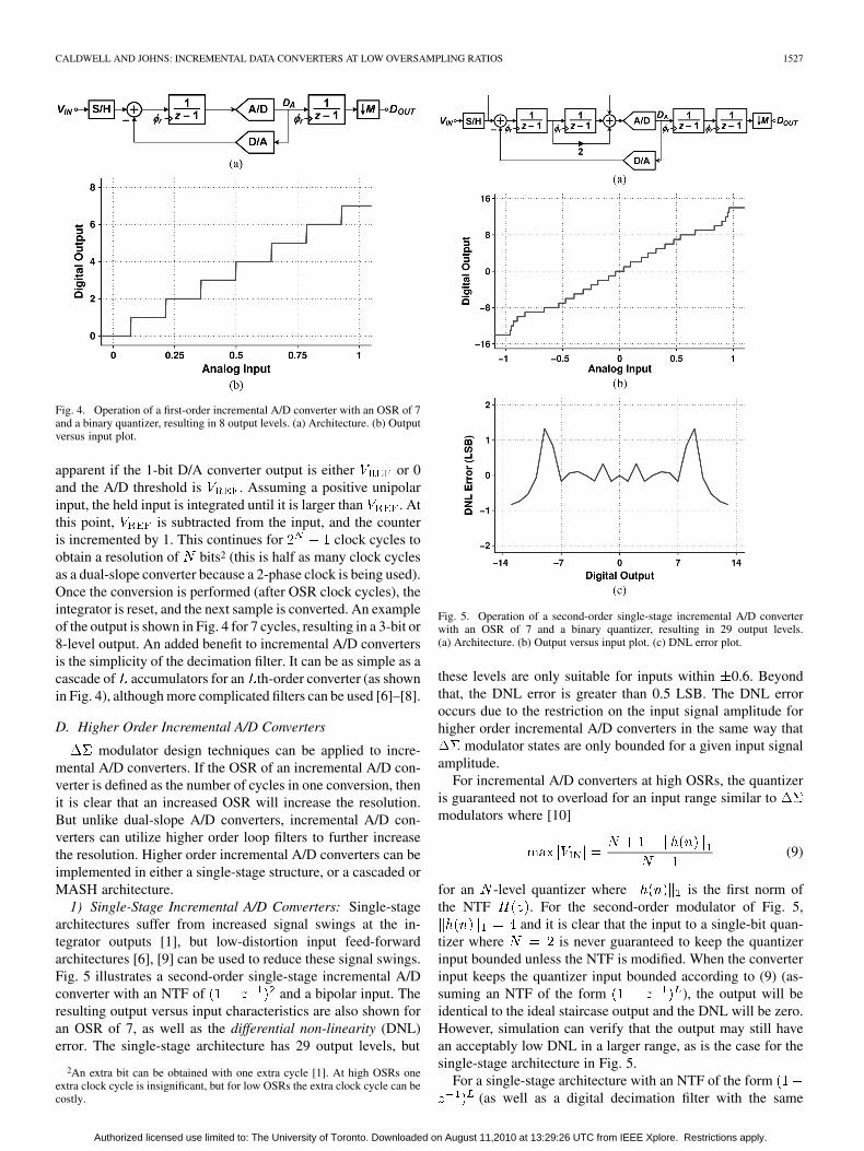
Fig. 4. Operation of a first-order incremental A/D converter with an OSR of 7and a binary quantizer, resulting in 8 output levels. (a) Architecture. (b) Outputversus input plot.
apparent if the 1-bit D/A converter output is either or 0and the A/D threshold is . Assuming a positive unipolarinput, the held input is integrated until it is larger than . Atthis point, is subtracted from the input, and the counteris incremented by 1. This continues for clock cycles toobtain a resolution of bits2 (this is half as many clock cyclesas a dual-slope converter because a 2-phase clock is being used).Once the conversion is performed (after OSR clock cycles), theintegrator is reset, and the next sample is converted. An exampleof the output is shown in Fig. 4 for 7 cycles, resulting in a 3-bit or8-level output. An added benefit to incremental A/D convertersis the simplicity of the decimation filter. It can be as simple as acascade of accumulators for an th-order converter (as shownin Fig. 4), although more complicated filters can be used [6]–[8].
D. Higher Order Incremental A/D Converters
modulator design techniques can be applied to incre-mental A/D converters. If the OSR of an incremental A/D con-verter is defined as the number of cycles in one conversion, thenit is clear that an increased OSR will increase the resolution.But unlike dual-slope A/D converters, incremental A/D con-verters can utilize higher order loop filters to further increasethe resolution. Higher order incremental A/D converters can beimplemented in either a single-stage structure, or a cascaded orMASH architecture.
1) Single-Stage Incremental A/D Converters: Single-stagearchitectures suffer from increased signal swings at the in-tegrator outputs [1], but low-distortion input feed-forwardarchitectures [6], [9] can be used to reduce these signal swings.Fig. 5 illustrates a second-order single-stage incremental A/Dconverter with an NTF of and a bipolar input. Theresulting output versus input characteristics are also shown foran OSR of 7, as well as the differential non-linearity (DNL)error. The single-stage architecture has 29 output levels, but
2An extra bit can be obtained with one extra cycle [1]. At high OSRs oneextra clock cycle is insignificant, but for low OSRs the extra clock cycle can becostly.
Fig. 5. Operation of a second-order single-stage incremental A/D converterwith an OSR of 7 and a binary quantizer, resulting in 29 output levels.(a) Architecture. (b) Output versus input plot. (c) DNL error plot.
these levels are only suitable for inputs within 0.6. Beyondthat, the DNL error is greater than 0.5 LSB. The DNL erroroccurs due to the restriction on the input signal amplitude forhigher order incremental A/D converters in the same way that
modulator states are only bounded for a given input signalamplitude.
For incremental A/D converters at high OSRs, the quantizeris guaranteed not to overload for an input range similar tomodulators where [10]
(9)
for an -level quantizer where is the first norm ofthe NTF . For the second-order modulator of Fig. 5,
and it is clear that the input to a single-bit quan-tizer where is never guaranteed to keep the quantizerinput bounded unless the NTF is modified. When the converterinput keeps the quantizer input bounded according to (9) (as-suming an NTF of the form ), the output will beidentical to the ideal staircase output and the DNL will be zero.However, simulation can verify that the output may still havean acceptably low DNL in a larger range, as is the case for thesingle-stage architecture in Fig. 5.
For a single-stage architecture with an NTF of the form(as well as a digital decimation filter with the same
Authorized licensed use limited to: The University of Toronto. Downloaded on August 11,2010 at 13:29:26 UTC from IEEE Xplore. Restrictions apply.

1528 IEEE TRANSACTIONS ON CIRCUITS AND SYSTEMS—I: REGULAR PAPERS, VOL. 57, NO. 7, JULY 2010
Fig. 6. Operation of a second-order cascaded incremental A/D converter withan OSR of 7 and binary quantizers, resulting in 32 output levels. (a) Architecture.(b) Output versus input plot.
transfer function), the resolution of the incremental A/D can befound using the following equation (see Appendix A)
dB (10)
for an th-order converter with quantizer levels and an OSRof . The coefficient is the maximum converter amplitudethat keeps the quantizer input bounded and is usually less thanunity.
2) Cascaded Incremental A/D Converters: Like modu-lators, the cascaded architecture is more stable for higher orderconverters. As opposed to feeding the output of the first inte-grator into the subsequent stage (as suggested in [1]), the firststage error can be fed into the following stage. This results insmaller signal amplitude being fed to the subsequent stage sinceit has less signal component, and facilitates the use of interstagegains and multi-bit quantizers to increase the SQNR.
Fig. 6 illustrates a second-order cascaded incremental A/Dconverter with an NTF of . For the same NTF as inFig. 5, the cascaded architecture has 30 output levels for an OSRof 7, and they form a perfect staircase output. Since an inputamplitude as large as unity keeps the quantizer input bounded,no DNL error occurs for the entire input range.
It can also be seen that the input extends beyond unity and theperfect staircase is still intact. DNL errors result due to quantizeroverload, but the quantizer in an incremental converter may notoverload at lower OSRs since it is reset every OSR clock cycles,meaning that the accumulation responsible for quantizer over-load is cut short, unlike in modulators. This allows slightlylarger full-scale inputs than would be expected for an equivalentNTF of a modulator.
The MASH architecture that will be discussed in this paperis an th-order cascade of first-order stages with an NTF (and
digital decimation filter) of . The resolution ofthis particular MASH architecture can be computed as (seeAppendix A)
dB (11)
where is the OSR, is the number of quantizer levels andis the product of the maximum converter input that keeps the
quantizer bounded for each stage. Since the first-order incre-mental A/D converter does not overload with inputs as large asunity, will be unity, or slightly larger. Eq. (11) assumes thatan interstage gain of is used between cascaded stages.
E. Input-Referred Noise
Calculating the input-referred noise of an incremental A/Dconverter is quite different from a modulator. Every conver-sion has a weighting associated with each sample, and for higherorder modulators earlier samples have a higher weighting thanlater samples because the digital filter has unequal weightingcoefficients for higher order modulators [6]. The total input-re-ferred noise power is
(12)
where is the input noise power of each sample, is the OSR(and number of samples per conversion), and is the weightingassociated with each sample.
In a first-order modulator, assuming an accumulator as a deci-mation filter, the weighting factors are equal sincethe output is effectively an average of the inputs added tothe quantization noise error introduced. The resulting input-re-ferred noise power is , as expected for an A/D converteroversampled by . But as the modulator order increases this isno longer the case. For a second-order modulator with a 2-stagecascaded accumulating decimation filter, the weighting factorsincrease to
(13)
The resulting total noise power is increased by a factor of up to4/3 [6] since
(14)
At an OSR of 1, this reduces to the expected , but for higherOSRs these higher order incremental A/D converters introducemore input-referred noise into the system when compared to
modulators, to a maximum of 33% more.The increased input-referred noise can be compared for mod-
ulators of various orders and OSRs, and the results are sum-marized in Table I. The results are normalized to the expectedinput-referred noise power of an oversampled A/D converterwhere the noise is for an OSR of . It is clear that at highOSRs, lower order incremental A/D converters must be used tokeep the input-referred noise power low. But when low OSRs
Authorized licensed use limited to: The University of Toronto. Downloaded on August 11,2010 at 13:29:26 UTC from IEEE Xplore. Restrictions apply.

CALDWELL AND JOHNS: INCREMENTAL DATA CONVERTERS AT LOW OVERSAMPLING RATIOS 1529
TABLE IRELATIVE INPUT-REFERRED NOISE POWER FOR INCREMENTAL A/D
CONVERTERS FOR INCREASING OSR AND ORDER
TABLE IICOMPARISON OF SECOND-ORDER�� AND INCREMENTAL A/D AT LOW OSRS
are used, there is a limit on the converter order to maintain agiven noise power.
III. INCREMENTAL DATA CONVERTERS AT LOW OSRS
A. Single-Stage and Cascaded
Like modulators, cascaded incremental architectureshave a much larger SQNR at low OSRs than single-stagearchitectures. But the reason is quite different, and this is whyit is best to think of incremental A/D converters at low OSRs asoperating distinctly from noise-shaping modulators.
When compared to modulators, incremental A/D con-verters will have one or more output levels for any non-zerovalues of , and according to (10) and (11). Unlikemodulators at low OSRs where noise shaping increases the totalquantization noise power of the system [10], incremental A/Dconverters will always have a minimum resolution equal to theresolution of the quantizer, even at an OSR of 1 (which will bediscussed in the next section).
Table II compares simulated SQNRs of a modulator andan incremental A/D converter at an OSR of 2, 4, 8 and 16 usingan NTF of with a second-order MASH architecture(with 3-level quantizers and an interstage gain of 2) as well asa second-order single-stage architecture (with a 5-level quan-tizer). At a low OSR of 2 and 4, the incremental A/D converterhas a larger SQNR, while at an OSR of 8, the results are verysimilar. At higher OSRs of 16 and above, the modulator hasa larger SQNR. These results motivate the use of incrementalA/D converters instead of modulators at lower OSRs.
As another example, Fig. 7 shows a comparison of theSQNR at increasing OSRs for an eighth-order cascaded ,an eighth-order cascaded incremental A/D converter, and an
Fig. 7. Simulated SQNR versus OSR for three different architectures. All threeA/D converters have the same internal 3-level quantizers. Simulations for theincremental A/D match equation (11).
8-stage pipeline A/D converter. Each stage has a 3-level quan-tizer so the three converters are almost identical architecturally.As long as the OSR is less than 5.3, the incremental A/Dconverter has a higher SQNR than the other two architectures.Above an OSR of 5.3, noise-shaping in a modulatoroutperforms incremental A/D conversion. It is also interestingto note that a modulator only outperforms a pipeline A/Dconverter at OSRs greater than 2.5; at lower OSRs modu-lators increase the total quantization noise power to an extentthat it is more beneficial to avoid noise-shaping altogether.
Incremental A/D converters and modulators operate ondifferent principles because the loop filter is reset and the inputis held in an incremental converter. Since the incremental A/Dconverter has less noise than a modulator at an OSR of 1 dueto the increased noise power from noise-shaping, it should notbe surprising that the incremental A/D converter outperformsthe modulator up until the OSR where noise-shaping beginsto improve the modulator’s resolution. Another reason forthe increased resolution (as mentioned in Section II-D) is thelarger allowable signal amplitudes. Since an incremental A/Dconverter resets after OSR clock cycles, the memory of previousconversions is lost, and thus a sustained large signal has onlyOSR clock cycles to accumulate in the integrator to overloadthe quantizer. Therefore, while a limits the signal ampli-tude at low OSRs as it would at high OSRs, an incremental A/Dconverter at low OSRs allows larger signal amplitudes than athigh OSRs since there are fewer cycles for the signal to accu-mulate. This can contribute a few extra dB of resolution as theOSR is lowered.
At an OSR of 3, these three architectures can also be com-pared while varying the number of stages. The results are shownin Fig. 8. At this OSR the incremental A/D converter outper-forms the modulator and pipeline A/D converter.
B. Pipeline Equivalency
As pointed out in the previous section, even with an OSRof 1, at very least the incremental A/D converter still resolvesthe input signal with the internal quantizer. If a cascaded incre-mental A/D converter is used, (11) predicts outputlevels for an th-order converter with -level quantizers. This
Authorized licensed use limited to: The University of Toronto. Downloaded on August 11,2010 at 13:29:26 UTC from IEEE Xplore. Restrictions apply.

1530 IEEE TRANSACTIONS ON CIRCUITS AND SYSTEMS—I: REGULAR PAPERS, VOL. 57, NO. 7, JULY 2010
Fig. 8. Simulated SQNR versus number of stages for three different architec-tures at an OSR of 3 with 3-level internal quantizers. For the incremental con-verter and �� modulator, the number of stages is equivalent to its order sincethey use a cascade of first-order stages. Again, simulations for the incrementalA/D match equation (11).
Fig. 9. The architectural similarity between the stages of a pipeline A/D con-verter and an input-feedforward cascaded incremental A/D converter. (a) Reset-ting gain stage. (b) Resetting integrating stage.
is identical to the resolution of an -stage pipeline A/D con-verter with -level internal quantizers. In fact, when the incre-mental A/D converter has an OSR of 1, it is effectively a pipelineA/D converter.
More specifically, an input feed-forward cascaded incre-mental A/D converter can be thought of as a higher orderpipeline A/D converter where the OSR determines how fre-quently the resetting is done. Architecturally the two are almostidentical; the main difference lies in designing a gain stage or anintegrating stage. A single stage of both architectures is shownFig. 9 and they are almost identical. The incremental A/D con-verter stage uses a resetting integrator while the pipeline A/Dconverter uses a gain stage which is effectively an integratorthat resets on every clock cycle . Also, the addition at theinput of the quantizer in the incremental converter occurs onall clock cycles except for the resetting phase . This is alsotrue for the pipeline converter stage, but since it resets on everyclock cycle, this addition is never performed.
At the circuit level, a resetting gain stage and a resetting inte-grating stage are shown in Fig. 10. The gain stage clock re-sets on , while the integrator clock resets on , but onlyevery th clock cycle (for an OSR of ). Aside from a couple
switches, the only difference lies in the resetting sequence. Withthe same and (a reasonable assumption since deter-mines the thermal noise, and controls the gain), both opera-tional transconductance amplifiers (OTAs) would be designedalmost identically.
C. Removing the Input S/H
An incremental A/D converter ideally requires a very accu-rate S/H circuit on the input. The design of this block can be verydifficult especially when trying to achieve better than 10-bit per-formance. The S/H can be removed from an incremental A/Dconverter, resulting in a modified STF. This can be understoodby analyzing a first-order converter.
In a single-bit first-order incremental A/D converter it willbe shown that the output of one conversion will always be thesame as long as the average of the input for that conversion isconstant (assuming no quantizer overload). For an input ,assuming an input feed-forward architecture, the input to thequantizer after the first clock cycles will be
...
(15)
If it is assumed that the converter is operating within the con-verter input range where the quantizer is not overloaded, then
. This also means that if the lastsample is included in the inequality,
(16)
which is equivalent to
(17)
For a given sum of the inputs throughout the cycles, there is a unique sum of digital outputs
that will keep (17) bounded within. As long as is constant, will be
constant. Since is simply the final digital output of the in-cremental A/D converter after going through the accumulatingdecimation filter, this will be a unique digital output as long asthe sum of the inputs is constant (which is equivalent tokeeping the average of the input samples constant).
If the input of the first-order incremental A/D converter isaveraged and then passed through a S/H, this system will beidentical to one where a moving input enters the system with noS/H since the output is only a function of the sum. For example,if three samples of a moving input 0.1, 0.2, and 0.3 enter thefirst integrator of the system (for an OSR of 3), it is identical toa held input of 0.2 entering the first integrator for three cycles.So the incremental A/D converter with a moving input can be
Authorized licensed use limited to: The University of Toronto. Downloaded on August 11,2010 at 13:29:26 UTC from IEEE Xplore. Restrictions apply.

CALDWELL AND JOHNS: INCREMENTAL DATA CONVERTERS AT LOW OVERSAMPLING RATIOS 1531
Fig. 10. The circuit-level difference between a pipeline A/D converter and an incremental A/D converter lies in the resetting sequence of the gain orintegrating stage. (a) Resetting gain stage. (b) Resetting integrating stage.
Fig. 11. Model of an incremental A/D converter with no S/H, and its equivalent model with an input S/H. ���� is not explicitly used, but it is the effectivemodification of the STF when the S/H is removed.
Fig. 12. Signal transfer function ���� for incremental A/D converters with an OSR of 3. The vertical dotted line is at the signal band edge � ��� �����.(a) First order. (b) Second order.
modeled as a typical incremental A/D converter where the S/His preceded by an averaging filter , as shown in Fig. 11.This provides a direct way to analyze the effect of the movinginput on an incremental A/D converter using the filter .
The filter , while not explicitly present in the incrementalA/D converter, effectively modifies the STF when the input S/His removed. Depending on the order of the modulator, willhave a different shape. The filter is of the form
(18)
for a first-order incremental with an OSR of and Fig. 12shows with an OSR of 3. Since the input signal is limitedto , the attenuation will be no larger than 3.52 dBat the edge of the signal band, represented by the vertical dotted
line in Fig. 12. The filter is a digital sinc filter similar to whatwas seen in the dual-slope A/D converter (which had no S/H).While input signals between and will stillalias back into the signal band, they will be attenuated accordingto the STF.
The discussion can be extended to find STFs of higher orderconverters with removed S/H blocks. For these architectures theSTF is a weighted sum of inputs that are held constant,resulting in a more complicated filter that is a weightedaverage of the inputs. The resulting equivalent filter for asecond-order incremental A/D converter with a moving input is
(19)
Authorized licensed use limited to: The University of Toronto. Downloaded on August 11,2010 at 13:29:26 UTC from IEEE Xplore. Restrictions apply.

1532 IEEE TRANSACTIONS ON CIRCUITS AND SYSTEMS—I: REGULAR PAPERS, VOL. 57, NO. 7, JULY 2010
Fig. 13. Half-delaying resetting scheme for two cascaded integrators in an incremental A/D converter. (a) Resetting integrator; (b) clocking (OSR of 3).
The STF of this incremental A/D converter for an OSR of 3 isalso shown in Fig. 12. The attenuation is 2.78 dB at the signalband edge. The attenuation at the edge of the signal band isless and will continue to reduce for higher order incrementalA/D converters with the input S/H removed. Generalizing toan th-order converter (assuming an th-order accumulatingdecimation filter equal to the NTF), the STF is
(20)
D. Resetting Efficiency
One difficulty in designing power efficient incremental A/Dconverters at low OSRs is the reset phase. The simple way toreset the converter is to do the same as is done in a pipeline A/Dconverter. If each stage is delayed by half a clock cycle (i.e.,odd stages are sampled on and even stages are sampled on
), then half a clock cycle is available to reset the integrator.As shown in Fig. 13, for the first stage the input is sampledon and integrated on and the opposite clock phases areused for the second stage. For an OSR of , on every thclock phase of the integrator is reset by , and the entire
clock phase is available to reset. Because the output of thefirst integrator will only be valid at the end of (due to theoccasional reset during ), the second integrator must sampleon . The corresponding reset switch will then reset onevery th clock phase of .
The resetting scheme of Fig. 13 is power inefficient becausewhen the subsequent stage has a similarly sized capacitor asthe current stage, additional loading occurs during the ampli-fying/integrating phase which is the phase that typically limitsthe OTA bandwidth. To charge the subsequent stage’s samplingcapacitance extra current must be drawn from the amplifier. Thisresults in a larger amplifier and a reduced feedback factor , fur-ther increasing the amplifier size for a given bandwidth.
At low OSRs, will likely be a significant fraction of andthis increased load on the first integrator stage will increase thesize of the OTA. An overdesign is required in the amplifying/in-tegrating phase while in the sampling phase the OTA simplyholds the current value and any power dissipated is wasted (al-though it cannot be turned off since it needs to hold the valueon the capacitor). This is wasteful since both stages have sig-nificantly different requirements on the current consumption;it is far more efficient when the requirements on both stagesare almost identical. The specific efficiencies are dependent onthe architecture and the number of quantizer levels, but usinghalf-delaying stages as opposed to full-delaying stages has thepotential to increase the power by more than a factor of 2.
As an example, if the second stage is designed to contributehalf the input-referred noise power of the first stage at an OSRof 3, then the second stage would be designed about 3 timessmaller and . Also, if the integrator coefficient ofthe first stage is 2, then . When the first stage is notloaded by the second stage, the OTA sees a feedback capaci-tance of . But when it is loaded by the second stage, thesampling capacitance of the second stage is addedto the feedback capacitance, resulting in a doubling of the totalcapacitance seen by the first stage OTA, and hence a doublingof the OTA power as well.
E. Calibration
The circuit performance requirements of a cascaded incre-mental A/D converter are quite stringent when high resolutionis desired, and calibration may be needed to achieve the full res-olution. Similar to a MASH modulator, the analog filtersmust match the digital filters to avoid any noise leakage fromearlier stages to the output. Some of the techniques presentedin [11] and [12] for calibrating MASH modulators can beapplied to incremental A/D converters to match the back-enddigital filter to the non-ideal analog filters.
Authorized licensed use limited to: The University of Toronto. Downloaded on August 11,2010 at 13:29:26 UTC from IEEE Xplore. Restrictions apply.

CALDWELL AND JOHNS: INCREMENTAL DATA CONVERTERS AT LOW OVERSAMPLING RATIOS 1533
Fig. 14. Digital calibrating filter for a cascaded incremental A/D converter. A third-order structure is shown for simplicity, but it can be easily extended to an�th-order modulator where � digital paths combine to a final � .
Fig. 15. Architecture for an eighth-order cascaded incremental A/D converter. The reset clocks are offset by one sample for each stage.
The coefficients that need calibration in an incremental A/Dconverter are similar to those of a cascaded modulator. Anon-ideal integrator can be modeled as [10]
(21)
where and are functions of the capacitor ratio and finite DCgain. If the cascaded incremental A/D converter is an ideal cas-cade of first-order modulators, then the back-end digital filter isas shown in Fig. 14 where the differentiators and accumulatorsare reset on the appropriate phases, and all of the coefficients
are unity. If the integrators are non-ideal so that the co-efficients characterize the th first-order modulator ac-cording to (21), then the back-end digital filter shown in Fig. 14will perfectly calibrate the incremental A/D converter. No noiseleakage will occur when the modulator is perfectly calibratedso that the only remaining error term will exist due to the errorof the last stage. For an th-order cascade of first-order mod-ulators oversampled by 3 with an input and an th-stagequantization error , the output is equal to (assuming aslowly varying input signal for simplicity)
(22)
where
(23)
and
(24)
The coefficient does not deviate much from unity since bothand are close to unity. However, the product of the coeffi-
cients that determine can reduce the signal amplitude slightly.For example, in an eighth-order modulator with integrator DCgains of 40 B and perfect capacitor matching, the signal will beattenuated by 2.10 dB.
IV. LOW OSR INCREMENTAL A/D CONVERTER EXAMPLE
This section will present a brief design example of a 12-bit(74 dB) incremental A/D converter, while also demonstratingits reconfigurability.
A. Architecture
As has been discussed, high-order cascaded architectures arebetter suited to low OSR incremental A/D design. The chosenarchitecture, shown in Fig. 15, is an eighth-order cascade of
Authorized licensed use limited to: The University of Toronto. Downloaded on August 11,2010 at 13:29:26 UTC from IEEE Xplore. Restrictions apply.

1534 IEEE TRANSACTIONS ON CIRCUITS AND SYSTEMS—I: REGULAR PAPERS, VOL. 57, NO. 7, JULY 2010
Fig. 16. STF for an eighth-order incremental A/D converter with an OSR of 3.
first-order stages with 3-level quantizers and an OSR of 3. Ithas a peak SQNR of 83.5 dB, 9.5 dB above the intended 74 dBresolution. Referring to Fig. 7, this architecture outperforms anequivalent architecture by 17 dB. The increased input noisedue to the uneven weighting of the input samples is 3.05 dB.The corresponding weighting parameters for this architectureare .
If it is designed with controllable resetting clocks, then for any OSR of , the clocks can be
adjusted to reset every clock cycles. If the OSR is set to1, the architecture becomes an 8-stage pipeline A/D converterwith 1.5 bits/stage. If desired, an extra 2-bit flash A/D couldbe added at the output of the last stage for a 10-bit pipelinearchitecture. If the OSR is set to infinity (i.e., the incrementalconverter never resets), the converter becomes an eighth-ordercascaded modulator [13]. The analog circuitry remainsthe same but the decimation filter would need to be modifieddepending on the intended OSR of the modulator. TheSQNR for both of these configurations were shown in Fig. 7.The chosen architecture can be reconfigured to realize any ofthe SQNR values on the plot by simply adjusting the resettingscheme.
B. STF
Assuming the S/H is removed, the STF of the eighth-ordercascaded incremental A/D converter with an OSR of 3 and3-level quantizers is shown in Fig. 16. The attenuation is 0.97dB at the edge of the signal band. This is relatively small andwould likely be considered a worthwhile trade-off since thehigh power S/H is no longer needed.
C. Calibration
The OTA gains of each stage must be high to keep the analogand digital filters matched, avoiding noise leakage. Otherwisecalibration must be used where the digital filter coefficients canbe calibrated to match the imperfect analog coefficients using atest signal injected in the quantizer [12]. The digital filter shownin Fig. 14 (extended to eighth-order) would be sufficient if the
and coefficients could be calibrated to 11 bit resolutionfor the first-stage, and progressively less for later stages. Fig. 17shows the spectrum of an incremental A/D converter before andafter calibration, assuming OTA gains of 40 dB. The slight at-tenuation of the input signal due to calibration is visible.
Fig. 17. Calibration of the proposed incremental A/D converter ���� ����� � . (a) Uncalibrated. (b) Calibrated.
V. CONCLUSION
In this paper, theory for designing incremental A/D con-verters at low OSRs was presented. It was shown that anincremental A/D converter has improved performance overa modulator at very low OSRs, and is equivalent to apipeline A/D converter when oversampled by unity. The impactof removing the input S/H was analyzed, as well as the reset-ting phase power efficiency. A sample modulator was shownto demonstrate the feasibility of low OSR incremental A/Dconverters.
APPENDIX A
The following will derive the number of output levels for anth-order incremental A/D converter with an NTF of
at an OSR of with an -level quantizer, and a digital dec-imation filter equal of . The A/D output isassumed to be between 1 (i.e., for ,
for , etc.), while the D/A output isthe same value multiplied by .
As a reference for the following derivations, an -level quan-tizer with upper and lower quantizer levels 1 can have aninput as large as without overloading the quan-tizer, meaning that the magnitude of the quantizer error is lessthan . Input feed-forward architectures are analyzed,but feedback architectures will yield the same number of outputlevels.
A. First Order
In Section III-C it was shown that after clock cycles, as-suming a converter input where the quantizer input is not over-loaded according to (9), the input to the quantizer is bounded by
where
(25)
Generalized to an -level quantizer, the quantizer input will bebounded by
(26)
The last digital output is the -level quantizedvalue of the input . As long as the inequality of (26)
Authorized licensed use limited to: The University of Toronto. Downloaded on August 11,2010 at 13:29:26 UTC from IEEE Xplore. Restrictions apply.

CALDWELL AND JOHNS: INCREMENTAL DATA CONVERTERS AT LOW OVERSAMPLING RATIOS 1535
Fig. 18. A second-order input feed-forward cascaded incremental A/D converter.
holds, the difference between the input and the outputmust be constrained by the inequality
(27)or equivalently,
(28)
Dividing both sides by and , the resulting inequality is
(29)
The digital output of the incremental A/D converter, scaled fordigital values between 1, is . Therefore,the inequality of (29) defines the error between the digital outputof the incremental A/D converter and the normalized input
. Since the error magnitude is less than ,and the error is uniformly distributed (as expected in a staircaseoutput similar to those shown in Fig. 4 and Fig. 6 and verifiedin simulation), the A/D converter has outputlevels.
B. Second-Order Single-Stage
Analyzing the second-order input feed-forward modulator ofFig. 5, the output of the first integrator is
...
(30)
The output of the second integrator is
...
(31)
The input to the quantizer is
(32)
Assuming keeps the quantizer input from overloading, theinput to the quantizer is again bounded according to
(33)
Adding the last digital output , the resulting in-equality (with some rearranging of (32)) is
(34)
Authorized licensed use limited to: The University of Toronto. Downloaded on August 11,2010 at 13:29:26 UTC from IEEE Xplore. Restrictions apply.

1536 IEEE TRANSACTIONS ON CIRCUITS AND SYSTEMS—I: REGULAR PAPERS, VOL. 57, NO. 7, JULY 2010
Dividing both sides by and , the inequalitybecomes
(35)
The scaled digital output of the second-order incre-mental A/D converter is .Therefore, the inequality again defines the error between thedigital output of the incremental converter and the normalizedinput. The error is less than , so the A/Dconverter has output levels.
C. Second-Order Cascaded
To analyze a second-order cascaded architecture, the inputfeed-forward modulator of Fig. 18 will be used. The first quan-tizer has levels while the second quantizer has levels.The output of the first integrator is
...
(36)
samples are taken since there is a delay from the inputto the second stage. The integrator output gets multiplied by thegain and becomes the input to the second integrator. The inputto the second quantizer becomes
...
(37)
Assuming that keeps the quantizer input from over-loading, and that the gain factor increases the error termfrom the previous stage such that the input to the second stagealso keeps the second quantizer input from overloading, thenthe input to the second quantizer is bounded according to
(38)
Adding the last digital output , the resultinginequality is
(39)
Dividing both sides by and , the inequalitybecomes
(40)
Referring to Fig. 18, the digital output of the second-order cascaded incremental A/D converter is
(41)
Since (no input has affected the second stage afterone sample), the resulting digital output is
(42)
This digital output is identical to the digital signal subtractedfrom the normalized input signal in the inequality of (40) (asidefrom the scaling factor of which keeps the digitalsignal between 1).
The inequality of (40) defines the error between the digitaloutput of the cascaded incremental converter and the normalizedinput, and the error is less than so theA/D converter has output levels.Since the first quantizer has -levels, if a converter input ofunity keeps the second stage quantizer bounded (as is the casefor this particular example), can be as large as , andthe resulting number of output levels is
(43)
Authorized licensed use limited to: The University of Toronto. Downloaded on August 11,2010 at 13:29:26 UTC from IEEE Xplore. Restrictions apply.
CALDWELL AND JOHNS: INCREMENTAL DATA CONVERTERS AT LOW OVERSAMPLING RATIOS 1537
D. Extension to Higher Order
For single-stage architectures the results can be generalizedto higher order converters and the number of output levels is
(44)
It can be seen that this equation works for previous cases, andit should be clear how the previous analysis can be extended tothird-order, fourth-order, and higher order converters (althoughit becomes quite tedious).
For cascaded architectures the results can also be general-ized to higher order converters. The equation is very similar tothat for the single-stage architecture, except that the number ofoutput levels is increased (roughly) by the gain factor associ-ated with each stage. The resulting number of output levels for
stages is
(45)
If the stages are all identical first-order stages where a full-scaleinput keeps the quantizers bounded, then assuming each stagequantizer has -levels, and , the resulting numberof output levels is
(46)
For an eighth-order cascaded incremental A/D converter withfirst-order 3-level quantizer stages, the number of output levelsis
(47)
as the OSR is varied. This is how the SQNR for the incre-mental A/D converter in Fig. 7 is found. It was also verified withsimulations and matched the predicted resolution.
REFERENCES
[1] J. Robert and P. Deval, “A second-order high-resolution incrementalA/D converter with offset and charge injection compensation,” IEEE J.Solid-State Circuits, vol. 23, pp. 736–741, Jun. 1988.
[2] V. Quiquempoix, P. Deval, A. Barreto, G. Bellini, J. Collings, J.Markus, J. Silva, and G. C. Temes, “A low-power 22-bit incrementalADC with 4 ppm INL, 2 ppm gain error and 2 uV DC offset,” in Proc.IEEE ESSCIRC, Sep. 2005, pp. 443–446.
[3] M. A. P. Pertijs, A. Niederkorn, X. Ma, B. McKillop, A. Bakker, and J.H. Huijsing, “A CMOS smart temperature sensor with a �� inaccuracyof�0.5 C from�50 C to 120 C,” IEEE J. Solid-State Circuits, vol. 40,no. 2, pp. 454–461, Feb. 2005.
[4] L. Rossi, S. Tanner, and P. Farine, “Performance analysis of a hybridincremental and cyclic A/D conversion principle,” IEEE Trans. CircuitsSyst. I, vol. 56, pp. 1383–1390, 2009.
[5] D. A. Johns and K. Martin, Analog Integrated Circuit De-sign. Toronto, Canada: Wiley, 1997.
[6] J. Markus, J. Silva, and G. C. Temes, “Theory and applications of in-cremental �� converters,” IEEE Trans. Circuits Syst. I, vol. 51, pp.678–690, Apr. 2004.
[7] S. Kavusi, H. Kakavand, and A. E. Gamal, “On incremental sigma-delta modulation with optimal filtering,” IEEE Trans. Circuits Syst. I,vol. 53, pp. 1004–1015, May 2006.
[8] J. Steensgaard, Z. Zhang, W. Yu, A. Sarhegyi, L. Lucchese, D. Kim,and G. C. Temes, “Noise-power optimization of incremental data con-verters,” IEEE Trans. Circuits Syst. I, vol. 55, pp. 1289–1296, 2008.
[9] J. Silva, U. Moon, J. Steensgaard, and G. C. Temes, “Wideband low-distortion delta-sigma ADC topology,” IEE Electron. Lett., vol. 37, pp.737–738, Jun. 2001.
[10] R. Schreier and G. C. Temes, Understanding Delta-Sigma Data Con-verters. Hoboken, NJ: Wiley, 2005.
[11] G. Cauwenberghs and G. C. Temes, “Adaptive digital correction ofanalog errors in MASH ADC’s—Part I: Off-line and blind on-line cal-ibration,” IEEE Trans. Circuits Syst. II, vol. 47, pp. 621–628, 2000.
[12] P. Kiss, J. Silva, A. Wiesbauer, T. Sun, U. Moon, J. T. Stonick, andG. C. Temes, “Adaptive digital correction of analog errors in MASHADC’s—Part II: Correction using test-signal injection,” IEEE Trans.Circuits Syst. II, vol. 47, pp. 629–638, 2000.
[13] O. J. A. P. Nys and E. Dijkstra, “On configurable oversampled A/Dconverters,” IEEE J. Solid-State Circuits, vol. 28, pp. 736–742, Jul.1993.
Trevor C. Caldwell (S’06) received the B.A.Sc.degree from the Division of Engineering Scienceand the M.A.Sc. degree from the Department ofElectrical and Computer Engineering at the Uni-versity of Toronto, Toronto, ON, Canada, in 2002and 2004, respectively. He is currently finishing hisPh.D. degree at the same university, and workingat Analog Devices in Toronto with the High-SpeedConverters group. His research interests focus onhigh-speed oversampled data converters.
Mr. Caldwell is the recipient of the National Sci-ences and Engineering Research Council of Canada (NSERC) Masters and Doc-toral postgraduate scholarships.
David A. Johns (S’81–M’89–SM’94–F’01) receivedthe B.A.Sc., M.A.Sc., and Ph.D. degrees from theUniversity of Toronto, Toronto, ON, Canada, in 1980,1983, and 1989, respectively.
In 1988, he was hired at the University of Torontowhere he is currently a full Professor. He has ongoingresearch programs in the general area of analog in-tegrated circuits with particular emphasis on digitalcommunications. His research work has resulted inmore than 40 publications as well as the 1999 IEEEDarlington Award. His is coauthor of a textbook en-
titled Analog Integrated Circuit Design (Wiley, 1997) and has given numerousindustrial short courses. Together with academic experience, he also has spent anumber of years in the semiconductor industry and is a co-founder of SnowbushMicroelectronics.
Dr. Johns served as a guest editor of the IEEE JOURNAL OF SOLID-STATE
CIRCUITS and an associate editor for IEEE TRANSACTIONS ON CIRCUITS AND
SYSTEMS II from 1993 to 1995 and for IEEE TRANSACTIONS ON CIRCUITS AND
SYSTEMS I from 1995 to 1997, and was elected to Adcom for SSCS in 2002.His homepage is http://www.eecg.toronto.edu/johns.
Authorized licensed use limited to: The University of Toronto. Downloaded on August 11,2010 at 13:29:26 UTC from IEEE Xplore. Restrictions apply.