Buck converters (integrated switch) | TI.com - Texas Instruments
21
FB EN V DD V IN 0.8V to 3.6V SGND GND LM3218 V OUT = 2.5 x V CON V IN C OUT C IN GND V OUT Integrated Inductor LM3218 V CON LM3218 www.ti.com SNOSB11B – MARCH 2008 – REVISED MARCH 2013 LM3218 650 mA Miniature, Adjustable, Step-Down DC-DC Converter for RF Power Amplifiers Check for Samples: LM3218 1FEATURES DESCRIPTION The LM3218 is a DC-DC converter with inductor 2• Includes 2.6 μH Inductor in Very Small Form which is optimized for powering RF power amplifiers Factor (3mm x 2.5mm x 1.2mm) (PAs) from a single Lithium-Ion cell. It steps down an • 2 MHz (typ.) PWM Switching Frequency input voltage in the range from 2.7V to 5.5V to an • Operates from a Single Li-Ion Cell (2.7V to adjustable output voltage of 0.8V to 3.6V. Output voltage is set by using a V CON analog input to control 5.5V) power levels and efficiency of the RF PA. • Adjustable Output Voltage (0.8V to 3.6V) The LM3218 offers superior electrical performance for • Fast Output Voltage Transient (0.8V to 3.4V in mobile phones and similar RF PA applications with a 25 μs typ.) reduced footprint (3mm x 2.5mm x 1.2mm). Fixed- • 650 mA Maximum Load Capability frequency PWM operation minimizes RF interference. • High Efficiency (95% typ. at 3.9 V IN , 3.4 V OUT at A shutdown function turns the device off and reduces 400 mA) battery consumption to 0.01 μA (typ.). • 8-pin POS Package The LM3218 is available in an integrated inductor • Current Overload Protection 8–pin POS package. A high switching frequency (2 MHz typ.) allows use of tiny surface-mount • Thermal Overload Protection components. Only two small external surface-mount components, two ceramic capacitors, are required. APPLICATIONS The overall board space is reduced up to 25% from • Cellular Phones the typical discrete inductor solution. • Hand-Held Radios • RF PC Cards • Battery-Powered RF Devices TYPICAL APPLICATION Figure 1. LM3218 Typical Application 1 Please be aware that an important notice concerning availability, standard warranty, and use in critical applications of Texas Instruments semiconductor products and disclaimers thereto appears at the end of this data sheet. 2All trademarks are the property of their respective owners. PRODUCTION DATA information is current as of publication date. Copyright © 2008–2013, Texas Instruments Incorporated Products conform to specifications per the terms of the Texas Instruments standard warranty. Production processing does not necessarily include testing of all parameters.
-
Upload
khangminh22 -
Category
Documents
-
view
0 -
download
0
Transcript of Buck converters (integrated switch) | TI.com - Texas Instruments
FB
EN
VDDVIN
0.8V to 3.6V
SGNDGND
LM3218
VOUT = 2.5 x VCON
VIN
COUT
CIN
GND
VOUT
Integrated InductorLM3218
VCON
LM3218
www.ti.com SNOSB11B –MARCH 2008–REVISED MARCH 2013
LM3218 650 mA Miniature, Adjustable, Step-Down DC-DC Converter for RF PowerAmplifiers
Check for Samples: LM3218
1FEATURES DESCRIPTIONThe LM3218 is a DC-DC converter with inductor
2• Includes 2.6 µH Inductor in Very Small Formwhich is optimized for powering RF power amplifiersFactor (3mm x 2.5mm x 1.2mm)(PAs) from a single Lithium-Ion cell. It steps down an
• 2 MHz (typ.) PWM Switching Frequency input voltage in the range from 2.7V to 5.5V to an• Operates from a Single Li-Ion Cell (2.7V to adjustable output voltage of 0.8V to 3.6V. Output
voltage is set by using a VCON analog input to control5.5V)power levels and efficiency of the RF PA.• Adjustable Output Voltage (0.8V to 3.6V)The LM3218 offers superior electrical performance for• Fast Output Voltage Transient (0.8V to 3.4V inmobile phones and similar RF PA applications with a25 µs typ.)reduced footprint (3mm x 2.5mm x 1.2mm). Fixed-• 650 mA Maximum Load Capability frequency PWM operation minimizes RF interference.
• High Efficiency (95% typ. at 3.9 VIN, 3.4 VOUT at A shutdown function turns the device off and reduces400 mA) battery consumption to 0.01 µA (typ.).
• 8-pin POS Package The LM3218 is available in an integrated inductor• Current Overload Protection 8–pin POS package. A high switching frequency (2
MHz typ.) allows use of tiny surface-mount• Thermal Overload Protectioncomponents. Only two small external surface-mountcomponents, two ceramic capacitors, are required.APPLICATIONS The overall board space is reduced up to 25% from
• Cellular Phones the typical discrete inductor solution.• Hand-Held Radios• RF PC Cards• Battery-Powered RF Devices
TYPICAL APPLICATION
Figure 1. LM3218 Typical Application
1
Please be aware that an important notice concerning availability, standard warranty, and use in critical applications ofTexas Instruments semiconductor products and disclaimers thereto appears at the end of this data sheet.
2All trademarks are the property of their respective owners.
PRODUCTION DATA information is current as of publication date. Copyright © 2008–2013, Texas Instruments IncorporatedProducts conform to specifications per the terms of the TexasInstruments standard warranty. Production processing does notnecessarily include testing of all parameters.
LM3218
SNOSB11B –MARCH 2008–REVISED MARCH 2013 www.ti.com
These devices have limited built-in ESD protection. The leads should be shorted together or the device placed in conductive foamduring storage or handling to prevent electrostatic damage to the MOS gates.
CONNECTION DIAGRAM
Figure 2. Package Number NQA0008A
PIN DESCRIPTIONSPin # Name Description
1 EN Enable Input. Set this digital input high for normal operation. For shutdown, set low.
2 VCON Voltage Control Analog input. VCON controls VOUT in PWM mode.
3 FB Feedback Analog Input. Connect to the VOUT pin.
4 SGND Analog and Control Ground.
5 VOUT Output Voltage, connects to one terminal of 2.6 µH inductor. Connect output filter capacitor C2 to get DCvoltage out.
6 PGND Power Ground
7 PVIN Power Supply Voltage Input to the internal Buck PFET switch.
8 VDD Analog Supply Input.
2 Submit Documentation Feedback Copyright © 2008–2013, Texas Instruments Incorporated
Product Folder Links: LM3218

LM3218
www.ti.com SNOSB11B –MARCH 2008–REVISED MARCH 2013
ABSOLUTE MAXIMUM RATINGS (1) (2) (3)
VDD, PVIN to SGND −0.2V to +6.0V
PGND to SGND −0.2V to +0.2V
EN, FB, VCON (SGND −0.2V)to (VDD +0.2V)
w/6.0V max
VOUT (PGND −0.2V)to (PVIN +0.2V)
w/6.0V max
PVIN to VDD −0.2V to +0.2V
Continuous Power Dissipation (4) Internally Limited
Junction Temperature (TJ-MAX) +150°C
Storage Temperature Range −65°C to +150°C
Maximum Lead Temperature(Soldering, 10 sec.) +260°C
ESD Rating (5) (6) Human Body Model: 2000V
Machine Model: 200V
(1) Absolute Maximum Ratings indicate limits beyond which damage to the component may occur. Operating Ratings are conditions underwhich operation of the device is ensured. Operating Ratings do not imply specified performance limits. For specified performance limitsand associated test conditions, see the Electrical Characteristics tables.
(2) All voltages are with respect to the potential at the GND pins. The LM3218 is designed for mobile phone applications where turn-on afterpower-up is controlled by the system controller and where requirements for a small package size overrule increased die size for internalUnder Voltage Lock-Out (UVLO) circuitry. Thus, it should be kept in shutdown by holding the EN pin low until the input voltage exceeds2.7V.
(3) If Military/Aerospace specified devices are required, please contact the TI Sales Office/Distributors for availability and specifications.(4) Internal thermal shutdown circuitry protects the device from permanent damage. Thermal shutdown engages at TJ = 150°C (typ.) and
disengages at TJ = 125°C (typ.).(5) The Human body model is a 100 pF capacitor discharged through a 1.5 kΩ resistor into each pin. (MIL-STD-883 3015.7) The machine
model is a 200 pF capacitor discharged directly into each pin.(6) TI recommends that all integrated circuits be handled with appropriate precautions. Failure to observe proper ESD handling procedures
can result in damage.
OPERATING RATINGS (1) (2)
Input Voltage Range 2.7V to 5.5V
Recommended Load Current 0 mA to 650 mA
Junction Temperature (TJ) Range −30°C to +125°C
Ambient Temperature (TA) Range (3) −30°C to +85°C
(1) Absolute Maximum Ratings indicate limits beyond which damage to the component may occur. Operating Ratings are conditions underwhich operation of the device is ensured. Operating Ratings do not imply specified performance limits. For specified performance limitsand associated test conditions, see the Electrical Characteristics tables.
(2) All voltages are with respect to the potential at the GND pins. The LM3218 is designed for mobile phone applications where turn-on afterpower-up is controlled by the system controller and where requirements for a small package size overrule increased die size for internalUnder Voltage Lock-Out (UVLO) circuitry. Thus, it should be kept in shutdown by holding the EN pin low until the input voltage exceeds2.7V.
(3) In applications where high power dissipation and/or poor package thermal resistance is present, the maximum ambient temperature mayhave to be de-rated. Maximum ambient temperature (TA-MAX) is dependent on the maximum operating junction temperature (TJ-MAX-OP =125°C), the maximum power dissipation of the device in the application (PD-MAX), and the junction-to ambient thermal resistance of thepart/package in the application (θJA), as given by the following equation: TA-MAX = TJ-MAX-OP – (θJA × PD-MAX).
THERMAL PROPERTIESJunction-to-Ambient Thermal 120°C/W
Resistance (θJA), NQA Package (1)
(1) Junction-to-ambient thermal resistance (θJA) is taken from thermal measurements, performed under the conditions and guidelines setforth in the JEDEC standard JESD51-7. A 4–layer, 4" x 4", 2/1/1/2 oz. Cu board as per JEDEC standards is used for the measurements.
Copyright © 2008–2013, Texas Instruments Incorporated Submit Documentation Feedback 3
Product Folder Links: LM3218
LM3218
SNOSB11B –MARCH 2008–REVISED MARCH 2013 www.ti.com
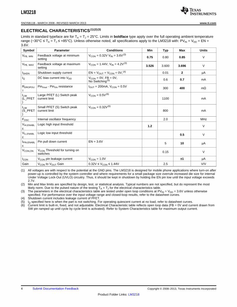
ELECTRICAL CHARACTERISTICS (1) (2) (3)
Limits in standard typeface are for TA = TJ = 25°C. Limits in boldface type apply over the full operating ambient temperaturerange (−30°C ≤ TA = TJ ≤ +85°C). Unless otherwise noted, all specifications apply to the LM3218 with: PVIN = VDD = EN =3.6V.
Symbol Parameter Conditions Min Typ Max Units
VFB, MIN Feedback voltage at minimum VCON = 0.32V VIN = 3.6V (3)0.75 0.80 0.85 Vsetting
VFB, MAX Feedback voltage at maximum VCON = 1.44V, VIN = 4.2V (3)3.526 3.600 3.696 Vsetting
ISHDN Shutdown supply current EN = VOUT = VCON = 0V, (4) 0.01 2 µA
IQ DC bias current into VDD VCON = 0V, FB = 0V, 0.6 0.7 mANo Switching (5)
RDROPOU PinVout - PinVin resistance IOUT = 200mA, VCON = 0.5V 300 400 mΩT
ILIM Large PFET (L) Switch peak VCON = 0.5V (6)
(L_PFET current limit 1100 mA)
ILIM Small PFET (S) Switch peak VCON = 0.32V (6)
(S_PFET current limit 800 mA)
FOSC Internal oscillator frequency 2.0 MHz
VIH,ENABL Logic high input threshold 1.2 VE
VIL,ENABL Logic low input threshold 0.5 VE
IPIN,ENABL Pin pull down current EN = 3.6V 5 10 µAE
VCON,ON VCON Threshold for turning on 0.15 Vswitches
ICON VCON pin leakage current VCON = 1.0V ±1 µA
Gain VCON to VOUT Gain 0.32V ≤ VCON ≤ 1.44V 2.5 V/V
(1) All voltages are with respect to the potential at the GND pins. The LM3218 is designed for mobile phone applications where turn-on afterpower-up is controlled by the system controller and where requirements for a small package size overrule increased die size for internalUnder Voltage Lock-Out (UVLO) circuitry. Thus, it should be kept in shutdown by holding the EN pin low until the input voltage exceeds2.7V.
(2) Min and Max limits are specified by design, test, or statistical analysis. Typical numbers are not specified, but do represent the mostlikely norm. Due to the pulsed nature of the testing TA = TJ for the electrical characteristics table.
(3) The parameters in the electrical characteristics table are tested under open loop conditions at PVIN = VDD = 3.6V unless otherwisespecified. For performance over the input voltage range and closed-loop results, refer to the datasheet curves.
(4) Shutdown current includes leakage current of PFET.(5) IQ specified here is when the part is not switching. For operating quiescent current at no load, refer to datasheet curves.(6) Current limit is built-in, fixed, and not adjustable. Electrical Characteristic table reflects open loop data (FB = 0V and current drawn from
SW pin ramped up until cycle by cycle limit is activated). Refer to System Characteristics table for maximum output current.
4 Submit Documentation Feedback Copyright © 2008–2013, Texas Instruments Incorporated
Product Folder Links: LM3218
LM3218
www.ti.com SNOSB11B –MARCH 2008–REVISED MARCH 2013
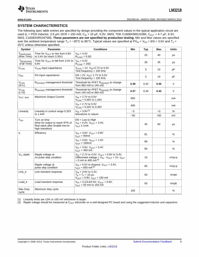
SYSTEM CHARACTERISTICSThe following spec table entries are specified by design providing the component values in the typical application circuit areused (L = POS Inductor, 2.6 µH; DCR = 150 mΩ; CIN = 10 µF, 6.3V, 0603, TDK C1608X5R0J106K; COUT = 4.7 µF, 6.3V,0603, C1608X5R0J475M). These parameters are not specified by production testing. Min and Max values are specifiedover the ambient temperature range TA = −30°C to 85°C. Typical values are specified at PVIN = VDD = EN = 3.6V and TA =25°C unless otherwise specified.
Symbol Parameter Conditions Min Typ Max Units
TRESPONSE Time for VOUT to rise from 0.8V VIN = 4.2V 25 40 µs(Rise Time) to 3.4V (to reach 3.35V) RLOAD = 5.5ΩTRESPONSE Time for VOUT to fall from 3.4V to VIN = 4.2V 35 45 µs(Fall Time) 0.8V RLOAD = 15Ω
CCON VCON input capacitance VCON = 1V, VIN=2.7V to 5.5V 5 10 pFTest frequency = 100 KHz
CEN EN input capacitance EN = 2V, VIN= 2.7V to 5.5V 5 10 pFTest frequency = 100 KHz
VCON RDSON(P) management threshold Threshold for PFET RDSON(P) to change 0.39 0.42 0.45 V(S>L) from 960 mΩ to 140 mΩVCON RDSON(P) management threshold Threshold for PFET RDSON(P) to change 0.37 0.40 0.43 V(L>S) from 140 mΩ to 960 mΩIOUT, MAX Maximum Output Current VIN = 2.7V to 5.5V 650 mAVCON = 0.45V to 1.44V
VIN = 2.7V to 5.5V 400 mAVCON = 0.32V to 0.45V
Linearity Linearity in control range 0.32V VIN = 3.9V (1) −3 +3 %to 1.44V Monotonic in nature −50 +50 mV
TON Turn on time EN = Low to High(time for output to reach 97% of VIN = 4.2V, VOUT = 3.4V, 40 60 µsfinal value after Enable low-to- IOUT ≤ 1mAhigh transition)
η Efficiency VIN = 3.6V, VOUT = 0.8V 81 %IOUT = 90mA
VIN = 3.6V, VOUT = 1.5V 89 %IOUT = 150mA
VIN = 3.9V, VOUT = 3.4V 95 %IOUT = 400 mA
VO_ripple Ripple voltage at VIN = 2.7V to 4.5V, VOUT = 0.8V to 3.4V,no pulse skip condition Differential voltage = VIN - VOUT > 1V, IOUT 10 mVp-p
= 0 mA to 400 mA (2)
Ripple voltage at VIN = 5.5V to dropout, VOUT = 3.4V, 60 mVp-ppulse skip condition IOUT = 650 mA (2)
Line_tr Line transient response VIN = 3.6V to 4.2V,TR = TF = 10 µs, 50 mVpkVOUT = 0.8V, IOUT = 100 mA
Load_tr Load transient response VIN = 3.1/3.6/4.5V, VOUT = 0.8V, 50 mVpkIOUT = 50 mA to 150 mA
Max Duty Maximum duty cycle 100 %cycle
(1) Linearity limits are ±3% or ±50 mV whichever is larger.(2) Ripple voltage should be measured at COUT electrode on a well-designed PC board and using the suggested inductor and capacitors.
Copyright © 2008–2013, Texas Instruments Incorporated Submit Documentation Feedback 5
Product Folder Links: LM3218

-40 -20 0 20 40 60 80 100
AMBIENT TEMPERATURE (ºC)
-3
-2
-1
0
1
2
3
SW
ITC
HIN
G F
RE
QU
EN
CY
VA
RIA
TIO
N (
%)
VIN = 5.5V
VIN = 4.2V
VIN = 3.6V
VIN = 2.7V
2.5 3.0 3.5 4.0 4.5 5.0 5.5 6.0
SUPPLY VOLTAGE (V)
OU
TP
UT
VO
LTA
GE
(V
)
IOUT = 50 mA
IOUT = 650 mA
IOUT = 300 mA
1.300
1.302
1.304
1.306
1.308
1.310
1.312
LM3218
SNOSB11B –MARCH 2008–REVISED MARCH 2013 www.ti.com
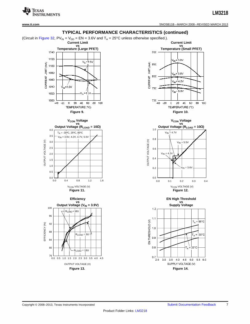
TYPICAL PERFORMANCE CHARACTERISTICS(Circuit in Figure 32, PVIN = VDD = EN = 3.6V and TA = 25°C unless otherwise specified.).
Quiescent Current Shutdown Currentvs vs
Supply Voltage (VCON = 0V, FB = 0V, No Switching) Temperature (VCON = 0V, EN = 0V)
Figure 3. Figure 4.
Switching Frequency Output Voltagevs vs
Temperature (VOUT = 1.3V, IOUT = 200 mA) Supply Voltage (VOUT = 1.3V)
Figure 5. Figure 6.
Output Voltage Output Voltagevs vs
Temperature (VIN = 3.6V, VOUT = 0.8V) Temperature (VIN = 4.2V, VOUT = 3.4V)
Figure 7. Figure 8.
6 Submit Documentation Feedback Copyright © 2008–2013, Texas Instruments Incorporated
Product Folder Links: LM3218
EF
FIC
IEN
CY
(%
)
0.0 0.5 1.0 1.5 2.0 2.5 3.0 3.5
OUTPUT VOLTAGE (V)
76
80
84
88
92
96
100
RLOAD = 5:
RLOAD = 10:
RLOAD = 15:
4.0 4.5
0.0 0.4 0.8 1.2 1.6
VCON VOLTAGE (V)
0.0
0.5
1.0
1.5
2.0
2.5
3.0
3.5
4.0
OU
TP
UT
VO
LTA
GE
(V
)
TA = -30ºC, 25ºC, 85ºC
VIN = 3.6V, 4.2V, 4.7V, 5.5V
0.0 0.1 0.2 0.3 0.4
VCON VOLTAGE (V)
0.0
0.2
0.4
0.6
0.8
1.0
OU
TP
UT
VO
LTA
GE
(V
)
VIN = 5.5V
VIN = 4.7V
VIN = 4.2V
VIN = 3.6V
LM3218
www.ti.com SNOSB11B –MARCH 2008–REVISED MARCH 2013
TYPICAL PERFORMANCE CHARACTERISTICS (continued)(Circuit in Figure 32, PVIN = VDD = EN = 3.6V and TA = 25°C unless otherwise specified.).
Current Limit Current Limitvs vs
Temperature (Large PFET) Temperature (Small PFET)
Figure 9. Figure 10.
VCON Voltage VCON Voltagevs vs
Output Voltage (RLOAD = 10Ω) Output Voltage (RLOAD = 10Ω)
Figure 11. Figure 12.
Efficiency EN High Thresholdvs vs
Output Voltage (VIN = 3.9V) Supply Voltage
Figure 13. Figure 14.
Copyright © 2008–2013, Texas Instruments Incorporated Submit Documentation Feedback 7
Product Folder Links: LM3218

IOUT
10 Ps/DIV
200 mA/DIVIL
VOUT 50 mV/DIVAC Coupled
VIN = 3.6V
VOUT = 0.8V
50 mA
250 mA
10 100 1000
OUTPUT CURRENT (mA)
EF
FIC
IEN
CY
(%
)
50
55
60
65
70
75
80
85
90
When VOUT = 1.0V (typical), Small PFET (960 m:). When VOUT = 1.05V (typical), Large PFET (140 m:).
VOUT = 1.0V
VOUT = 1.05V
VIN = 5.5V
VIN = 3.6V
VIN = 2.7V
10 100 1000
OUTPUT CURRENT (mA)
EF
FIC
IEN
CY
(%
)
40
45
50
55
60
65
70
75
80
85
90
V IN = 4.5V, VOUT = 1.05V
V IN = 4.5V, VOUT = 1.0V
When VOUT = 1.0V (typical), Small PFET (960 m:). When VOUT = 1.05V (typical), Large PFET (140 m:).
0 100 200 300 400 500 600 700
OUTPUT CURRENT (mA)
80
82
84
86
88
90
92
94
96
98
100
EF
FIC
IEN
CY
(%
)
VIN = 4.5V
VIN = 3.9V
VIN = 5.5V
LM3218
SNOSB11B –MARCH 2008–REVISED MARCH 2013 www.ti.com
TYPICAL PERFORMANCE CHARACTERISTICS (continued)(Circuit in Figure 32, PVIN = VDD = EN = 3.6V and TA = 25°C unless otherwise specified.).
Efficiency Efficiencyvs vs
Output Current (VOUT = 0.8V) Output Current (VOUT = 3.6V)
Figure 15. Figure 16.
Efficiency Efficiencyvs vs
Output Current (RDSON Management) Output Current (RDSON Management, VIN=4.5V)
Dark curves are efficiency profiles of either large PFETor small PFET whichever is higher.
Figure 17. Figure 18.
VIN-VOUTvs Load Transient Response
Output Current (100% Duty Cycle) (VOUT = 0.8V)
Figure 19. Figure 20.
8 Submit Documentation Feedback Copyright © 2008–2013, Texas Instruments Incorporated
Product Folder Links: LM3218
IOUT
10 Ps/DIV
200 mA/DIVIL
VOUT100 mV/DIVAC Coupled
VIN = 4.2V
VOUT = 3.4V
100 mA
400 mA
LM3218
www.ti.com SNOSB11B –MARCH 2008–REVISED MARCH 2013
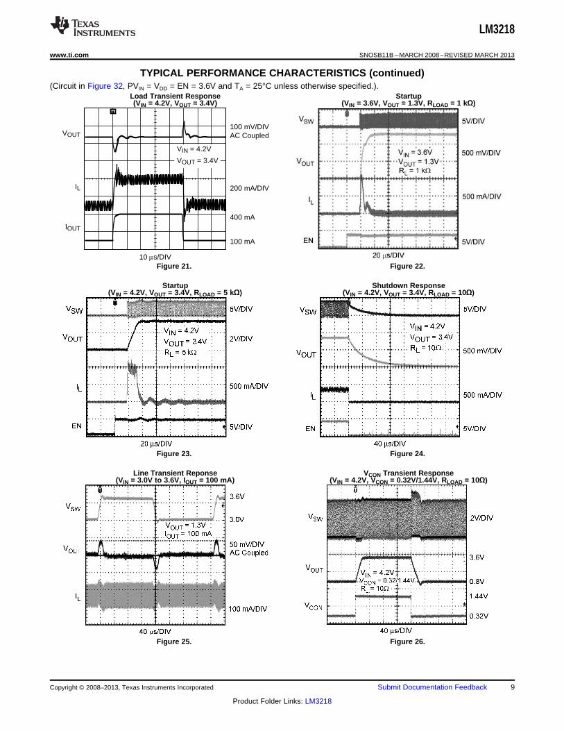
TYPICAL PERFORMANCE CHARACTERISTICS (continued)(Circuit in Figure 32, PVIN = VDD = EN = 3.6V and TA = 25°C unless otherwise specified.).
Load Transient Response Startup(VIN = 4.2V, VOUT = 3.4V) (VIN = 3.6V, VOUT = 1.3V, RLOAD = 1 kΩ)
Figure 21. Figure 22.
Startup Shutdown Response(VIN = 4.2V, VOUT = 3.4V, RLOAD = 5 kΩ) (VIN = 4.2V, VOUT = 3.4V, RLOAD = 10Ω)
Figure 23. Figure 24.
Line Transient Reponse VCON Transient Response(VIN = 3.0V to 3.6V, IOUT = 100 mA) (VIN = 4.2V, VCON = 0.32V/1.44V, RLOAD = 10Ω)
Figure 25. Figure 26.
Copyright © 2008–2013, Texas Instruments Incorporated Submit Documentation Feedback 9
Product Folder Links: LM3218
LM3218
SNOSB11B –MARCH 2008–REVISED MARCH 2013 www.ti.com
TYPICAL PERFORMANCE CHARACTERISTICS (continued)(Circuit in Figure 32, PVIN = VDD = EN = 3.6V and TA = 25°C unless otherwise specified.).
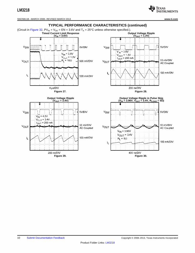
Timed Current Limit Response Output Voltage Ripple(VIN = 3.6V) (VOUT = 1.3V)
Figure 27. Figure 28.
Output Voltage Ripple Output Voltage Ripple in Pulse Skip(VOUT = 3.4V) (VIN = 3.96V, VOUT = 3.4V, RLOAD = 5Ω)
Figure 29. Figure 30.
10 Submit Documentation Feedback Copyright © 2008–2013, Texas Instruments Incorporated
Product Folder Links: LM3218

MOSFETCONTROL
LOGIC
CURRENTCOMP
OSCILLATOR
ERRORAMPLIFIER
DELAYLOGIC
VCON
FB
SHUTDOWNCONTROL
MAIN CONTROL
EN
FET SIZECONTROL
COMP
PVIN
PGND
VDD
SGND
SMALLPFET
LARGEPFET
VOUT
IntegratedInductor
LM3218
www.ti.com SNOSB11B –MARCH 2008–REVISED MARCH 2013
BLOCK DIAGRAM
Figure 31. Functional Block Diagram
Copyright © 2008–2013, Texas Instruments Incorporated Submit Documentation Feedback 11
Product Folder Links: LM3218
FB
EN
VDDPVIN
SGNDPGND
LM3218
Integrated Inductor
PA
VOUT
VCON
VIN
TX_ON/OFF
DAC
RF_ON/OFF
RFIC
RFin4.7 PF
VREF
VCC
10 PF
LM3218
SNOSB11B –MARCH 2008–REVISED MARCH 2013 www.ti.com
OPERATION DESCRIPTION
The LM3218 is a simple, step-down DC-DC converter with a 2.6 µH series inductor substrate optimized forpowering RF power amplifiers (PAs) in mobile phones, portable communicators, and similar battery powered RFdevices. It is designed to allow the RF PA to operate at maximum efficiency over a wide range of power levelsfrom a single Li-Ion battery cell. It is based on current mode buck architecture, with synchronous rectification forhigh efficiency. It is designed for a maximum load capability of 650 mA when VOUT > 1.05V (typ.) and 400 mAwhen VOUT < 1.00V (typ.) in PWM mode.
Maximum load range may vary from this depending on input voltage, output voltage and the inductor chosen.
Efficiency is typically around 95% for a 400 mA load with 3.4V output, 3.9V input. The LM3218 has an RDSONmanagement scheme to increase efficiency when VOUT ≤ 1V. The output voltage is dynamically programmablefrom 0.8V to 3.6V by adjusting the voltage on the control pin without the need for external feedback resistors.This prolongs battery life by changing the PA supply voltage dynamically depending on its transmitting power.
Additional features include current overload protection and thermal overload shutdown.
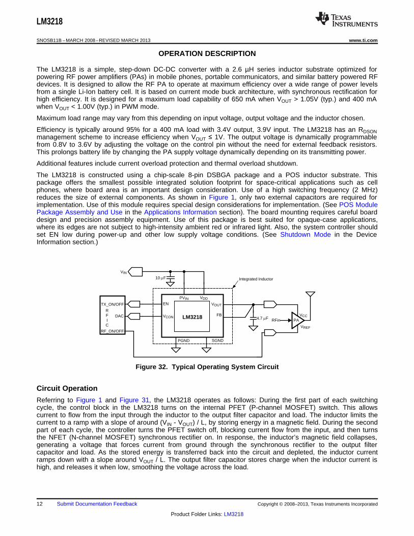
The LM3218 is constructed using a chip-scale 8-pin DSBGA package and a POS inductor substrate. Thispackage offers the smallest possible integrated solution footprint for space-critical applications such as cellphones, where board area is an important design consideration. Use of a high switching frequency (2 MHz)reduces the size of external components. As shown in Figure 1, only two external capacitors are required forimplementation. Use of this module requires special design considerations for implementation. (See POS ModulePackage Assembly and Use in the Applications Information section). The board mounting requires careful boarddesign and precision assembly equipment. Use of this package is best suited for opaque-case applications,where its edges are not subject to high-intensity ambient red or infrared light. Also, the system controller shouldset EN low during power-up and other low supply voltage conditions. (See Shutdown Mode in the DeviceInformation section.)
Figure 32. Typical Operating System Circuit
Circuit Operation
Referring to Figure 1 and Figure 31, the LM3218 operates as follows: During the first part of each switchingcycle, the control block in the LM3218 turns on the internal PFET (P-channel MOSFET) switch. This allowscurrent to flow from the input through the inductor to the output filter capacitor and load. The inductor limits thecurrent to a ramp with a slope of around (VIN - VOUT) / L, by storing energy in a magnetic field. During the secondpart of each cycle, the controller turns the PFET switch off, blocking current flow from the input, and then turnsthe NFET (N-channel MOSFET) synchronous rectifier on. In response, the inductor’s magnetic field collapses,generating a voltage that forces current from ground through the synchronous rectifier to the output filtercapacitor and load. As the stored energy is transferred back into the circuit and depleted, the inductor currentramps down with a slope around VOUT / L. The output filter capacitor stores charge when the inductor current ishigh, and releases it when low, smoothing the voltage across the load.
12 Submit Documentation Feedback Copyright © 2008–2013, Texas Instruments Incorporated
Product Folder Links: LM3218
LM3218
www.ti.com SNOSB11B –MARCH 2008–REVISED MARCH 2013
The output voltage is regulated by modulating the PFET switch on time to control the average current sent to theload. The effect is identical to sending a duty-cycle modulated rectangular wave formed by the power MOSFETswitch and synchronous rectifier to a low-pass filter formed by the inductor and output filter capacitor. The outputvoltage is equal to the average voltage at the terminal of the power MOSFET inverter.
While in operation, the output voltage is regulated by switching at a constant frequency and then modulating theenergy per cycle to control power to the load. Energy per cycle is set by modulating the PFET switch on-timepulse width to control the peak inductor current. This is done by comparing the signal from the current-senseamplifier with a slope compensated error signal from the voltage-feedback error amplifier. At the beginning ofeach cycle, the clock turns on the PFET switch, causing the inductor current to ramp up. When the current sensesignal ramps past the error amplifier signal, the PWM comparator turns off the PFET switch and turns on theNFET synchronous rectifier, ending the first part of the cycle. If an increase in load pulls the output down, theerror amplifier output increases, which allows the inductor current to ramp higher before the comparator turns offthe PFET. This increases the average current sent to the output and adjusts for the increase in the load. Beforeappearing at the PWM comparator, a slope compensation ramp from the oscillator is subtracted from the errorsignal for stability of the current feedback loop. The minimum on time of PFET is 55 ns (typ.)
Shutdown Mode
Setting the EN digital pin low (<0.5V) places the LM3218 in shutdown mode (0.01 µA typ.). During shutdown, thePFET switch, NFET synchronous rectifier, reference voltage source, control and bias circuitry of the LM3218 areturned off. Setting EN high (>1.2V) enables normal operation.
EN should be set low to turn off the LM3218 during power-up and under-voltage conditions when the powersupply is less than the 2.7V minimum operating voltage. The LM3218 is designed for compact portableapplications, such as mobile phones. In such applications, the system controller determines power supplysequencing and requirements for small package size outweigh the additional size required for inclusion of UVLO(Under Voltage Lock-Out) circuitry.
Internal Synchronous Rectification
While in PWM mode, the LM3218 uses an internal NFET as a synchronous rectifier to reduce rectifier forwardvoltage drop and associated power loss. Synchronous rectification provides a significant improvement inefficiency whenever the output voltage is relatively low compared to the voltage drop across an ordinary rectifierdiode.
The internal NFET synchronous rectifier is turned on during the inductor current down slope in the second part ofeach cycle. The synchronous rectifier is turned off prior to the next cycle. The NFET is designed to conductthrough its intrinsic body diode during transient intervals before it turns on, eliminating the need for an externaldiode.
RDSON(P) Management
The LM3218 has a unique RDSON(P) management function to improve efficiency in the low output current regionup to 100 mA. When the VCON voltage is less than 0.40V (typ.), the device uses only a small part of the PFET tominimize drive loss of the PFET. When VCON is greater than 0.42V (typ.), the entire PFET is used to minimizeRDSON(P) loss. This threshold has about 20 mV (typ.) of hysteresis.
VCON,ON
The output is disabled when VCON is below 125 mV (typ.). It is enabled when VCON is above 150 mV (typ.). Thethreshold has about 25 mV (typ.) of hysteresis.
Current Limiting
A current limit feature allows the LM3218 to protect itself and external components during overload conditions. InPWM mode, an 1100 mA (typ.) cycle-by-cycle current limit is normally used when VCON is above 0.42V (typ.),and an 800 mA (typ.) is used when VCON is below 0.40V (typ.). If an excessive load pulls the output voltage downto approximately 0.375V, then the device switches to a timed current limit mode when VCON is above 0.42V(typ.). In timed current limit mode the internal PFET switch is turned off after the current comparator trips and thebeginning of the next cycle is inhibited for 3.5us to force the instantaneous inductor current to ramp down to asafe value. The synchronous rectifier is off in timed current limit mode. Timed current limit prevents the loss ofcurrent control seen in some products when the output voltage is pulled low in serious overload conditions.
Copyright © 2008–2013, Texas Instruments Incorporated Submit Documentation Feedback 13
Product Folder Links: LM3218

LM3218
SNOSB11B –MARCH 2008–REVISED MARCH 2013 www.ti.com
Dynamically Adjustable Output Voltage
The LM3218 features dynamically adjustable output voltage to eliminate the need for external feedback resistors.The output can be set from 0.8V to 3.6V by changing the voltage on the analog VCON pin. This feature is useful inPA applications where peak power is needed only when the handset is far away from the base station or whendata is being transmitted. In other instances, the transmitting power can be reduced. Hence the supply voltage tothe PA can be reduced, promoting longer battery life. See Setting the Output Voltage in the ApplicationInformation section for further details. The LM3218 moves into Pulse Skipping mode when duty cycle is over92% and the output voltage ripple increases slightly.
Thermal Overload Protection
The LM3218 has a thermal overload protection function that operates to protect itself from short-term misuse andoverload conditions. When the junction temperature exceeds around 150°C, the device inhibits operation. Boththe PFET and the NFET are turned off in PWM mode. When the temperature drops below 125°C, normaloperation resumes. Prolonged operation in thermal overload conditions may damage the device and isconsidered bad practice.
APPLICATION INFORMATION
SETTING THE OUTPUT VOLTAGE
The LM3218 features a pin-controlled variable output voltage to eliminate the need for external feedbackresistors. It can be programmed for an output voltage from 0.8V to 3.6V by setting the voltage on the VCON pin,as in the following formula:
VOUT = 2.5 x VCON (1)
When VCON is between 0.32V and 1.44V, the output voltage will follow proportionally by 2.5 times of VCON.
If VCON is over 1.44V (VOUT = 3.6V), sub-harmonic oscillation may occur because of insufficient slopecompensation. If VCON voltage is less than 0.32V (VOUT = 0.8V), the output voltage may not be regulated due tothe required on-time being less than the minimum on-time (55 ns). The output voltage can go lower than 0.8Vproviding a limited VIN range is used. Refer to datasheet curve (VCON Voltage vs Output Voltage) for details. Thiscurve is for a typical part and there could be part-to-part variation for output voltages less than 0.8V over thelimited VIN range. When the control pin voltage is more than 0.15V (typ.), the switches are turned on. When it isless than 0.125V (typ.), the switches are turned off. This on/off function has 25 mV (typ.) hysteresis. Thequiescent current when (VCON = 0V and VEN = Hi) is around 600 µA.
ESTIMATION OF MAXIMUM OUTPUT CURRENT CAPABILITY
Referring to Figure 32, the Inductor peak-to-peak ripple current can be estimated by:IIND_PP = (VIN - VOUT ) × VOUT / (L1 × FSW × VIN) (2)
Where, Fsw is switching frequency.
Therefore, maximum output current can be calculated by:IOUT_MAX = ILIM - 0.5 × IIND_PP (3)
For the worst case calculation, the following parameters should be used:
FSW (Lowest switching frequency): 1.8 MHz
ILIM (Lowest current limit value): 985 mA
L1 (Lowest inductor value): refer to inductor datasheet. Note that inductance will drop with DC bias current andtemperature. The worst case is typically at 85°C.
For example, VIN = 4.2V, VOUT = 3.2V, L1 = 2.0 µH (Inductance value at 985 mA DC-bias current and 85°C), FSW= 1.8 MHz , ILIM = 985 mA.
IIND_PP = 212 mA (4)IOUT_MAX = 985 – 106 = 876 mA (5)
14 Submit Documentation Feedback Copyright © 2008–2013, Texas Instruments Incorporated
Product Folder Links: LM3218
LM3218
www.ti.com SNOSB11B –MARCH 2008–REVISED MARCH 2013
The effects of switch, inductor resistance and dead time are ignored. In real application, the ripple current wouldbe 10% to 15% higher than ideal case. This should be taken into account when calculating maximum outputcurrent. Special attention needs to be paid that a delta between maximum output current capability and thecurrent limit is necessary to satisfy transient response requirements. In practice, transient response requirementsmay not be met for output current greater than 650 mA.
INDUCTOR SELECTION
The inductor is an integrated POS 2.6 µH substrate within the LM3218 module and has a saturation currentrating over 1200 mA. The integrated inductor’s low 1.2 mm maximum height provides ease of use into smalldesign constraints. Integrating the inductor can eliminate layout issues associated with DC/DC converters andreduce potential EMI problems.
CAPACITOR SELECTION
The LM3218 is designed for use with ceramic capacitors for its input and output filters. Use a 10 µF ceramiccapacitor for input and a 4.7 µF ceramic capacitor for output. They should maintain at least 50% capacitance atDC bias and temperature conditions. Ceramic capacitor types such as X5R, X7R and B are recommended forboth filters. Table 1 lists some suggested part numbers and suppliers. DC bias characteristics of the capacitorsmust be considered when selecting the voltage rating and case size of the capacitor. If it is necessary to choosea 0603-size capacitor for CIN and COUT, the operation of the LM3218 should be carefully evaluated on the systemboard. Use of multiple 2.2 µF or 1 µF capacitors in parallel may also be considered.
Table 1. Suggested Capacitors And Their Suppliers
Model Vendor
C1608X5R0J106K, 10 µF, 6.3V TDK
C1608X5R0J475M, 4.7 µF, 6.3V TDK
0805ZD475KA 4.7 µF, 10V AVX
The input filter capacitor supplies AC current drawn by the PFET switch of the LM3218 in the first part of eachcycle and reduces the voltage ripple imposed on the input power source. The output filter capacitor absorbs theAC inductor current, helps maintain a steady output voltage during transient load changes and reduces outputvoltage ripple. These capacitors must be selected with sufficient capacitance and sufficiently low ESR(Equivalent Series Resistance) to perform these functions. The ESR of the filter capacitors is generally a majorfactor in voltage ripple.
EN PIN CONTROL
Drive the EN pin using the system controller to turn the LM3218 ON and OFF. Use a comparator, Schmidt triggeror logic gate to drive the EN pin. Set EN high (>1.2V) for normal operation and low (<0.5V) for a 0.01 μA (typ.)shutdown mode and requirements for small package size outweigh the additional size required for inclusion ofUVLO (Under Voltage Lock-Out) circuitry.
POS PACKAGE ASSEMBLY AND USE
The POS Integrated Inductor with LM3218 DSBGA package is optimized for the smallest possible size inapplications with red or infrared opaque cases. Because the DSBGA package lacks the plastic encapsulationcharacteristic of larger devices, it is vulnerable to light. Backside metalization and/or epoxy coating, along withfront-side shading by the printed circuit board, reduce this sensitivity. However, the package has exposed dieedges. In particular, DSBGA devices are sensitive to light, in the red and infrared range, shining on thepackage’s exposed die edges. The maximum shelf life after opening the dry pack is 168 hours, no bake allowedas it will further degrade the solder ability.
Copyright © 2008–2013, Texas Instruments Incorporated Submit Documentation Feedback 15
Product Folder Links: LM3218

FB
EN
VDDPVIN
VCON
SW
VIN
2.7V to 5.5V
VOUT
10 PF
4.7 PFSGNDPGND
2.6 PHC1
C2
L1
E
C
i
i
Fosc = 2 MHz
+
+
-
-
LM3218
SNOSB11B –MARCH 2008–REVISED MARCH 2013 www.ti.com
BOARD LAYOUT CONSIDERATIONS
Figure 33. Current Loop
The LM3218 converts higher input voltage to lower output voltage with high efficiency. This is achieved with aninductor-based switching topology. During the first half of the switching cycle, the internal PMOS switch turns on,the input voltage is applied to the inductor, and the current flows from PVIN line into the output capacitor and theload through the inductor. During the second half cycle, the PMOS turns off and the internal NMOS turns on. Theinductor current continues to flow via the inductor from the device PGND line into the output capacitor and theload.
Referring to Figure 33, a pulse current flows in the left-hand side loop, and a ripple current flows in the right-handside loop. Board layout and circuit pattern design of these two loops are the key factors for reducing noiseradiation and stable operation. In other lines, such as from battery to C1 and C2 to the load, the current is mostlyDC current. Therefore, it is not necessary to take so much care. Only pattern width (current capability) and DCRdrop considerations are needed.
Figure 34. Evaluation Board Layout
16 Submit Documentation Feedback Copyright © 2008–2013, Texas Instruments Incorporated
Product Folder Links: LM3218

LM3218
www.ti.com SNOSB11B –MARCH 2008–REVISED MARCH 2013
REVISION HISTORY
Changes from Revision A (March 2013) to Revision B Page
• Changed layout of National Data Sheet to TI format .......................................................................................................... 16
Copyright © 2008–2013, Texas Instruments Incorporated Submit Documentation Feedback 17
Product Folder Links: LM3218

PACKAGE OPTION ADDENDUM
www.ti.com 7-Jul-2014
Addendum-Page 1
PACKAGING INFORMATION
Orderable Device Status(1)
Package Type PackageDrawing
Pins PackageQty
Eco Plan(2)
Lead/Ball Finish(6)
MSL Peak Temp(3)
Op Temp (°C) Device Marking(4/5)
Samples
LM3218SEE/NOPB OBSOLETE POS NQA 8 TBD Call TI Call TI
LM3218SEX/NOPB OBSOLETE POS NQA 8 TBD Call TI Call TI (1) The marketing status values are defined as follows:ACTIVE: Product device recommended for new designs.LIFEBUY: TI has announced that the device will be discontinued, and a lifetime-buy period is in effect.NRND: Not recommended for new designs. Device is in production to support existing customers, but TI does not recommend using this part in a new design.PREVIEW: Device has been announced but is not in production. Samples may or may not be available.OBSOLETE: TI has discontinued the production of the device.
(2) Eco Plan - The planned eco-friendly classification: Pb-Free (RoHS), Pb-Free (RoHS Exempt), or Green (RoHS & no Sb/Br) - please check http://www.ti.com/productcontent for the latest availabilityinformation and additional product content details.TBD: The Pb-Free/Green conversion plan has not been defined.Pb-Free (RoHS): TI's terms "Lead-Free" or "Pb-Free" mean semiconductor products that are compatible with the current RoHS requirements for all 6 substances, including the requirement thatlead not exceed 0.1% by weight in homogeneous materials. Where designed to be soldered at high temperatures, TI Pb-Free products are suitable for use in specified lead-free processes.Pb-Free (RoHS Exempt): This component has a RoHS exemption for either 1) lead-based flip-chip solder bumps used between the die and package, or 2) lead-based die adhesive used betweenthe die and leadframe. The component is otherwise considered Pb-Free (RoHS compatible) as defined above.Green (RoHS & no Sb/Br): TI defines "Green" to mean Pb-Free (RoHS compatible), and free of Bromine (Br) and Antimony (Sb) based flame retardants (Br or Sb do not exceed 0.1% by weightin homogeneous material)
(3) MSL, Peak Temp. - The Moisture Sensitivity Level rating according to the JEDEC industry standard classifications, and peak solder temperature.
(4) There may be additional marking, which relates to the logo, the lot trace code information, or the environmental category on the device.
(5) Multiple Device Markings will be inside parentheses. Only one Device Marking contained in parentheses and separated by a "~" will appear on a device. If a line is indented then it is a continuationof the previous line and the two combined represent the entire Device Marking for that device.
(6) Lead/Ball Finish - Orderable Devices may have multiple material finish options. Finish options are separated by a vertical ruled line. Lead/Ball Finish values may wrap to two lines if the finishvalue exceeds the maximum column width.
Important Information and Disclaimer:The information provided on this page represents TI's knowledge and belief as of the date that it is provided. TI bases its knowledge and belief on informationprovided by third parties, and makes no representation or warranty as to the accuracy of such information. Efforts are underway to better integrate information from third parties. TI has taken andcontinues to take reasonable steps to provide representative and accurate information but may not have conducted destructive testing or chemical analysis on incoming materials and chemicals.TI and TI suppliers consider certain information to be proprietary, and thus CAS numbers and other limited information may not be available for release.
In no event shall TI's liability arising out of such information exceed the total purchase price of the TI part(s) at issue in this document sold by TI to Customer on an annual basis.

PACKAGE OPTION ADDENDUM
www.ti.com 7-Jul-2014
Addendum-Page 2

MECHANICAL DATA
NQA0008A
www.ti.com
SE08A (Rev D)

IMPORTANT NOTICETexas Instruments Incorporated and its subsidiaries (TI) reserve the right to make corrections, enhancements, improvements and otherchanges to its semiconductor products and services per JESD46, latest issue, and to discontinue any product or service per JESD48, latestissue. Buyers should obtain the latest relevant information before placing orders and should verify that such information is current andcomplete. All semiconductor products (also referred to herein as “components”) are sold subject to TI’s terms and conditions of salesupplied at the time of order acknowledgment.TI warrants performance of its components to the specifications applicable at the time of sale, in accordance with the warranty in TI’s termsand conditions of sale of semiconductor products. Testing and other quality control techniques are used to the extent TI deems necessaryto support this warranty. Except where mandated by applicable law, testing of all parameters of each component is not necessarilyperformed.TI assumes no liability for applications assistance or the design of Buyers’ products. Buyers are responsible for their products andapplications using TI components. To minimize the risks associated with Buyers’ products and applications, Buyers should provideadequate design and operating safeguards.TI does not warrant or represent that any license, either express or implied, is granted under any patent right, copyright, mask work right, orother intellectual property right relating to any combination, machine, or process in which TI components or services are used. Informationpublished by TI regarding third-party products or services does not constitute a license to use such products or services or a warranty orendorsement thereof. Use of such information may require a license from a third party under the patents or other intellectual property of thethird party, or a license from TI under the patents or other intellectual property of TI.Reproduction of significant portions of TI information in TI data books or data sheets is permissible only if reproduction is without alterationand is accompanied by all associated warranties, conditions, limitations, and notices. TI is not responsible or liable for such altereddocumentation. Information of third parties may be subject to additional restrictions.Resale of TI components or services with statements different from or beyond the parameters stated by TI for that component or servicevoids all express and any implied warranties for the associated TI component or service and is an unfair and deceptive business practice.TI is not responsible or liable for any such statements.Buyer acknowledges and agrees that it is solely responsible for compliance with all legal, regulatory and safety-related requirementsconcerning its products, and any use of TI components in its applications, notwithstanding any applications-related information or supportthat may be provided by TI. Buyer represents and agrees that it has all the necessary expertise to create and implement safeguards whichanticipate dangerous consequences of failures, monitor failures and their consequences, lessen the likelihood of failures that might causeharm and take appropriate remedial actions. Buyer will fully indemnify TI and its representatives against any damages arising out of the useof any TI components in safety-critical applications.In some cases, TI components may be promoted specifically to facilitate safety-related applications. With such components, TI’s goal is tohelp enable customers to design and create their own end-product solutions that meet applicable functional safety standards andrequirements. Nonetheless, such components are subject to these terms.No TI components are authorized for use in FDA Class III (or similar life-critical medical equipment) unless authorized officers of the partieshave executed a special agreement specifically governing such use.Only those TI components which TI has specifically designated as military grade or “enhanced plastic” are designed and intended for use inmilitary/aerospace applications or environments. Buyer acknowledges and agrees that any military or aerospace use of TI componentswhich have not been so designated is solely at the Buyer's risk, and that Buyer is solely responsible for compliance with all legal andregulatory requirements in connection with such use.TI has specifically designated certain components as meeting ISO/TS16949 requirements, mainly for automotive use. In any case of use ofnon-designated products, TI will not be responsible for any failure to meet ISO/TS16949.Products ApplicationsAudio www.ti.com/audio Automotive and Transportation www.ti.com/automotiveAmplifiers amplifier.ti.com Communications and Telecom www.ti.com/communicationsData Converters dataconverter.ti.com Computers and Peripherals www.ti.com/computersDLP® Products www.dlp.com Consumer Electronics www.ti.com/consumer-appsDSP dsp.ti.com Energy and Lighting www.ti.com/energyClocks and Timers www.ti.com/clocks Industrial www.ti.com/industrialInterface interface.ti.com Medical www.ti.com/medicalLogic logic.ti.com Security www.ti.com/securityPower Mgmt power.ti.com Space, Avionics and Defense www.ti.com/space-avionics-defenseMicrocontrollers microcontroller.ti.com Video and Imaging www.ti.com/videoRFID www.ti-rfid.comOMAP Applications Processors www.ti.com/omap TI E2E Community e2e.ti.comWireless Connectivity www.ti.com/wirelessconnectivity
Mailing Address: Texas Instruments, Post Office Box 655303, Dallas, Texas 75265Copyright © 2014, Texas Instruments Incorporated