An alternative solution to capacitive power supply using buck
Upload
khangminh22Category
view
0download
0
ISSN (Print) : 2320 – 3765 ISSN (Online): 2278 – 8875
International Journal of Advanced Research in Electrical, Electronics and Instrumentation Engineering An ISO 3297: 2007 Certified Organization Vol. 4, Special Issue 1, March 2015
National Conference on Recent Advances in Electrical & Electronics Engineering (NCREEE 2015)
Organized by
Dept. of EEE, Mar Baselios Institute of Technology & Science (MBITS), Kothamangalam, Kerala-686693, India On 26th & 27th March 2015
Copyright to IJAREEIE www.ijareeie.com 8
Design and Simulation of Two Phase Interleaved Buck Converter
Ashna Joseph1, Jebin Francis2
Assistant Professor, Dept. of EEE, MBITS, Kothamangalam, India 1
Assistant Professor, Dept. of EEE, RSET, Cochin, India 2
ABSTRACT: Interleaved Buck DC DC converters have presently acquired a wide importance owing to their application in voltage regulator modules. Interleaved Buck Converter (IBC) is adopted as a good solution for low voltage and high current applications. This paper presents the design of two phase interleaved buck converter and closed loop simulation of IBC against sudden variations in supply voltage conditions. Operating principle of IBC for (D<0.5) along with waveforms are clearly illustrated in this paper and it has been successfully verified using MATLAB simulink. KEYWORDS: Buck converter, Interleaving Technique, Two Phase Interleaved Buck Converter, Continuous Conduction Mode.
I.INTRODUCTION
Investigation of interleaving technique for step down topology mainly points out the benefits interleaving offers to future microprocessors. Most of today’s Voltage Regulator Modules (VRMs), which are used to power the microprocessors in computers, make use of conventional buck or synchronous buck topology [1]. At present, VRMs require output voltage lower than 1 V while output currents above 100A or so which makes the existing topologies inadequate. One of the circuits that are suitable for the low-voltage/ high-current output is an interleaved dc-dc converter. Interleaved Buck converters have proved to be very beneficial for future VRMs [1]-[6]. Interleaving can be thought of as a method of paralleling converters. In a broader view, interleaving means that N identical converters are connected in parallel as in Fig. 1 and the current through each switch is dispersed. When each converter provides the same current as the non-interleaved converter, the output current is N times higher. Therefore, the interleaved dc-dc converter is suitable to the low-voltage/high-current applications. Moreover, when the driving signals of N converters have 2π/N phase-shift one another, the output filter of the converter could be downsized [2]. Using interleaving, power stage of a converter is divided into several and smaller power stages thereby reducing the size of each component [7].
Fig. 1 Illustration of Interleaved Converter

ISSN (Print) : 2320 – 3765 ISSN (Online): 2278 – 8875
International Journal of Advanced Research in Electrical, Electronics and Instrumentation Engineering An ISO 3297: 2007 Certified Organization Vol. 4, Special Issue 1, March 2015
National Conference on Recent Advances in Electrical & Electronics Engineering (NCREEE 2015)
Organized by
Dept. of EEE, Mar Baselios Institute of Technology & Science (MBITS), Kothamangalam, Kerala-686693, India On 26th & 27th March 2015
Copyright to IJAREEIE www.ijareeie.com 9
The main goal of this paper is to present the state space analysis of two-cell IBC operating in continuous conduction mode (CCM) with D<0.5 .Section II presents operating principle of the IBC in CCM and section III discusses the design aspects of interleaved buck converter , Sections IV and V contain simulation results. Finally, paper is concluded in Section VI.
II. OPERATING PRINCIPLE – IBC The circuit diagram of IBC is given as shown in Fig. 2. This is equivalent to a parallel combination of two sets of switches, diodes and inductors connected to a common filter capacitor and load [6].The switches are operated 1800 out of phase. Assume the converter operates with duty ratio less than 50% and in continuous conduction mode (CCM).
Fig. 2 circuit diagram of 2 phase IBC
A two phase IBC will operate in four different modes and is explained as follows: Mode 1: In mode 1 switch Q1 is turned on by giving a gate pulse. At the same time switch Q2 is off. Current flows through the switch Q1, inductor L1 and load, making current through L1 to increase as long as Q1 is turned on. During this time current in L2 decreases linearly. The equivalent circuit is as in Fig. 2.a. The variations of iL1 and iL2 during T1 are given by,
(1)
(2)
Fig. 2(a) Equivalent Circuit of IBC in Mode 1

ISSN (Print) : 2320 – 3765 ISSN (Online): 2278 – 8875
International Journal of Advanced Research in Electrical, Electronics and Instrumentation Engineering An ISO 3297: 2007 Certified Organization Vol. 4, Special Issue 1, March 2015
National Conference on Recent Advances in Electrical & Electronics Engineering (NCREEE 2015)
Organized by
Dept. of EEE, Mar Baselios Institute of Technology & Science (MBITS), Kothamangalam, Kerala-686693, India On 26th & 27th March 2015
Copyright to IJAREEIE www.ijareeie.com 10
Mode 2: Since IBC operates with a duty cycle less than 0.5, in this mode both the switches are OFF. Diodes D1 and D2 are the conducting devices. The equivalent circuit is illustrated in Fig. 2.b.The energies stored in L1 and L2 are released to the load through the forward biased diodes. So iL1 and iL2 are decreased linearly. Thus the variations in iL1 and iL2 during T2 are given by,
(3)
(4)
Fig. 2(b) Equivalent Circuit of IBC in Mode 2 Mode 3: During T3 Q2 is turned On and Q1 turned off. The equivalent circuit is illustrated in Fig. 2.c. The turning on of Q2 charges the inductor L2 and since Q1 is off inductor L1 is discharged to the load..The variations in iL1 and iL2 during T3 are given by,
(5)
(6)
Equation (5) shows iL1 linearly decreasing during T3 since the slope is negative and a constant.
Fig. 2(c) Equivalent Circuit of IBC in Mode 3 Mode 4: The operating mode is same as mode 2. The variations in iL1 and iL2 during T4 are given as in equation (3) and (4).

ISSN (Print) : 2320 – 3765 ISSN (Online): 2278 – 8875
International Journal of Advanced Research in Electrical, Electronics and Instrumentation Engineering An ISO 3297: 2007 Certified Organization Vol. 4, Special Issue 1, March 2015
National Conference on Recent Advances in Electrical & Electronics Engineering (NCREEE 2015)
Organized by
Dept. of EEE, Mar Baselios Institute of Technology & Science (MBITS), Kothamangalam, Kerala-686693, India On 26th & 27th March 2015
Copyright to IJAREEIE www.ijareeie.com 11
Fig.3 Inductor Current Waveforms
III. DESIGN OF IBC
Here in Interleaved converters discrete components are typically placed in parallel to split/share the current stresses. The total load current Io Amperes is split into two power trains. So the effective load current for each power train is set to = .The current ripple ratio for each of the two stages is represented as ‘r’ and the swing is r x .
a.Inductor and Output Current
Looking at the total inductor current as depicted in Fig. 3 in section II, the combined output current has a repetition rate of 2f where f is the switching frequency. Its duty cycle is not D but 2D.It is because the ON time for each converter has remained the same, but the effective time period has been cut to half. So, the effective duty cycle for the total inductor current is
[8]. Since, peak to peak ripple in each phase is proportional to 1-D; the total current ripple in inductor is given by,
Total Inductor Ripple Current ( =
i.e, Alternatively stated,
The inductor design equation is similar to that of conventional Buck converter, with the exception that L here
is the total inductance value.
Ie,

ISSN (Print) : 2320 – 3765 ISSN (Online): 2278 – 8875
International Journal of Advanced Research in Electrical, Electronics and Instrumentation Engineering An ISO 3297: 2007 Certified Organization Vol. 4, Special Issue 1, March 2015
National Conference on Recent Advances in Electrical & Electronics Engineering (NCREEE 2015)
Organized by
Dept. of EEE, Mar Baselios Institute of Technology & Science (MBITS), Kothamangalam, Kerala-686693, India On 26th & 27th March 2015
Copyright to IJAREEIE www.ijareeie.com 12
And inductors in both the phases can be taken as L1=L2=L/2 b. OutputCapacitor
The capacitor design equation is the same as in conventional Buck converter except that instead of the switching frequency (f), the frequency here effectively doubles i.e., it becomes 2f. Thus output capacitor value is given by:
Parameter Value Number of Phases 2 Input Voltage, Vs 12 V Output Voltage,Vo 1.2 V Switching Frequency, f (per Phase) 100 kHz Per phase Ripple current , 10% Output Current,Io 12A Indutors per phase,L1,L2 22.5 µH
Output voltage ripple, ≤ 20 mV
Output Capacitor, C 10 µF
Table.1 Design Values of Two Phase IBC
IV. CLOSED LOOP SIMULATION OF TWO PHASE IBC Based on the design values of various parameters of IBC, a simulink model operating in open loop and closed loop is developed using Sim Power System Tool Box. To investigate the performance of IBC against variations in supply voltage , simulation is carried out and results of both steady state and transient conditions are presented
V. RESULT AND DISCUSSION
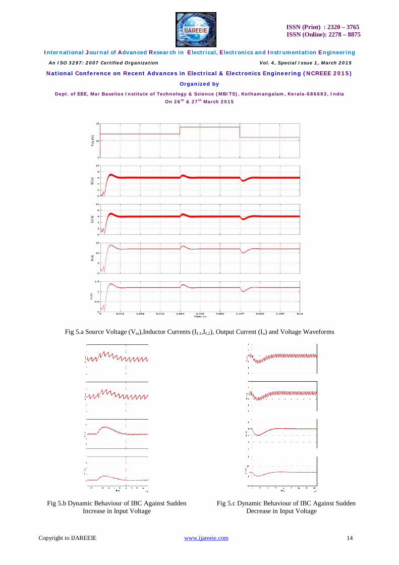
The open loop simulation result shown in Fig 4.a and 4.b throws an insight into the reduction of ripple in the total inductor current. From the steady state waveform of iL in Fig 4.b, frequency doubling can also be observed. In order to investigate the performance of IBC against input supply variations, sudden increase in input voltage from12V to 14 V at 0.004 s is done. Fig 5.a clearly illustrates all parameters of two phase IBC, with input source voltage variations from 12 V to 14V at 0.004 seconds and a sudden decrease in supply voltage from 14 V to 11 V in 0.007 seconds. Dynamic Response of two phase IBC with input supply variations is shown in Figs 5.b and. 5.c. Fig. 5.b gives the dynamic response against increase in voltage from 12 to 14 volts at time 0.004sec till 0.007 sec. Figure 5.c gives the dynamic response with decrease in voltage from 14 to 11 volts at time 0.007sec till 0.01 sec.

ISSN (Print) : 2320 – 3765 ISSN (Online): 2278 – 8875
International Journal of Advanced Research in Electrical, Electronics and Instrumentation Engineering An ISO 3297: 2007 Certified Organization Vol. 4, Special Issue 1, March 2015
National Conference on Recent Advances in Electrical & Electronics Engineering (NCREEE 2015)
Organized by
Dept. of EEE, Mar Baselios Institute of Technology & Science (MBITS), Kothamangalam, Kerala-686693, India On 26th & 27th March 2015
Copyright to IJAREEIE www.ijareeie.com 13
ISSN (Print) : 2320 – 3765 ISSN (Online): 2278 – 8875
International Journal of Advanced Research in Electrical, Electronics and Instrumentation Engineering An ISO 3297: 2007 Certified Organization Vol. 4, Special Issue 1, March 2015
National Conference on Recent Advances in Electrical & Electronics Engineering (NCREEE 2015)
Organized by
Dept. of EEE, Mar Baselios Institute of Technology & Science (MBITS), Kothamangalam, Kerala-686693, India On 26th & 27th March 2015
Copyright to IJAREEIE www.ijareeie.com 14
Fig 5.a Source Voltage (Vin),Inductor Currents (IL1,IL2), Output Current (Io) and Voltage Waveforms
Fig 5.b Dynamic Behaviour of IBC Against Sudden Increase in Input Voltage
Fig 5.c Dynamic Behaviour of IBC Against Sudden Decrease in Input Voltage

ISSN (Print) : 2320 – 3765 ISSN (Online): 2278 – 8875
International Journal of Advanced Research in Electrical, Electronics and Instrumentation Engineering An ISO 3297: 2007 Certified Organization Vol. 4, Special Issue 1, March 2015
National Conference on Recent Advances in Electrical & Electronics Engineering (NCREEE 2015)
Organized by
Dept. of EEE, Mar Baselios Institute of Technology & Science (MBITS), Kothamangalam, Kerala-686693, India On 26th & 27th March 2015
Copyright to IJAREEIE www.ijareeie.com 15
VI.CONCLUSION
An interleaved DC DC step - down converter for low output voltage and high output current suitable for VRM application is presented here. The paper explains clearly the operating principle of two phase IBC with equivalent circuits. A prototype circuit of the proposed converter with 12 V input voltage, 1. 2 V output voltage and 12 A output current is simulated and steady state ripple waveforms are obtained. The doubling of effective frequency in the total inductor cuurent is also illustrated here. The performance of IBC against sudden variations in supply voltage is also investigated and simulation results are clearly illustrated in the paper.
REFERENCES
1. Xunwei Zhou, Pit-Leong Wong,Peng Xu, Fred C. Lee and Alex Q. Huang. Motoki, " Investigation of Candidate VRM Topologies for Future Microprocessors,” IEEE Transactions on Power Electronics, vol. 15, no. 6, pp.1172-1182, Nov 2000.
2. Sheng Ye, Wilson Eberle and Yan-Fei Liu, “A Novel Non-Isolated Full Bridge Topology for VRM Applications,” IEEE Transactions on Power Electronics, vol. 23, no. 1, pp. 427-437, Jan 2008.
3. Oscar García, Pablo Zumel, Angel de Castro and José A. Cobos, “Automotive DC–DC Bidirectional Converter Made With Many Interleaved Buck Stages” IEEE Transactions On Power Electronics, Vol. 21, No. 3, pp.578-586, May 2006.
4. QingshuiLuzi, Xiancheng Wang and Issa Batarseh, “Large signal compensation network design for VRM Transient response improvement” in 31st Annual Conference of Industrial Electronics society ,IECON 2005,pp. 1139-1143,Nov2005
5. Yuri Panov and Milan M. Jovanovic´ “Design Considerations for 12-V/1.5-V, 50-A Voltage Regulator Modules,” IEEE Transactions on Power Electronics, vol. 16, no. 6, pp. 776-783, Nov. 2001.
6. DodiGarinto, “A Novel Multiphase Multi-Interleaving Buck Converters for Future Microprocessors,” in 12thInternational Power Electronics and Motion Control Conference, PEMC 2006, pp. 82-87 , Aug-sep 2006.
7. Daniel W Hart, “Power Electronics” Tata McGraw Hills, 2011, pp 237-238,467. 8. Sanjaya Maniktala, “Switching Power Converters A-Z” Elsevier, 2012, pp. 520- 524.
Copyright © 2022 FDOKUMEN