design, analysis and implementation of an interleaved pfc ...

IEEE TRANSACTIONS ON CIRCUITS AND SYSTEMS—I: REGULAR PAPERS, VOL. 61, NO. 2, FEBRUARY 2014 573
Time Interleaved RF CarrierModulations and Demodulations
Kwang-Jin Koh, Member, IEEE, Seyed Yahya Mortazavi, Student Member, IEEE, andSadia Afroz, Student Member, IEEE
Abstract—This paper proposes a time-interleaved RF car-rier modulation and demodulation technique, suitable for highfrequency mixer applications under a constraint of active de-vice speed limitation. The presents are in essence mixer arrayswhere modulated outputs by a series of time-delayed carrierswith a reduced frequency, compared with a carrier frequencyin fundamental mixers, will be interleaved in the time domainto synthesize the final output. The mixer arrays inherit an FIRfiltering function, and the time interleaving process is equivalentto the filtering process where the arrays select the fundamentaltone or its harmonics of a carrier in a periodic manner. Thecarrier waveform and duty-cycle play important roles in the noiseperformance of the mixer arrays. A comprehensive noise analysisis presented in this paper for both cases of correlated-noise anduncorrelated-noise mixer arrays. To minimize output noise power,optimization of carrier duty-cycle and noise filtering techniquehave been proposed and analyzed extensively for various types ofcarrier pulse. Finally analytical mismatch models are providedand output SNR degradations under finite mismatches amongstmixer array elements have been discussed based on the mismatchmodels. All theoretical analyses are verified through behav-ioral mixer array simulations including Monte-Carlo statisticalsimulations.
Index Terms—Array, demodulator, FIR filter, mixer, mixerarray, modulator, multiphase, radio frequency, time interleaving,transversal filter, wireless communications.
I. INTRODUCTION
R ECENTLY wireless communications at millimeter(mm)-wave and submillimeter wave ranges have been
gaining growing attentions to achieve a high data-rate overseveral 10’s Gb/s [1]–[3]. One of key technical huddles inrealizing the high-speed communications in integrated circuittechnologies is the carrier modulation and demodulation, dueto a lack of carrier source having a high spectral purity with anadequate output power at such high frequencies. To circumventthe issue from a system perspective, heterodyne architectureshave been adopted to reduce required carrier frequency at theexpense of a hardware complexity and image issue involved inthe double conversions [4]–[6]. A subharmonic mixing (e.g.,2x, 4x even-harmonic carrier modulation) has been anotherpopular choice for a minimum amount of signal processingat the mm-waves and therefore to relieve the speed burden
Manuscript received February 12, 2013; revisedMay 17, 2013; accepted June24, 2013. Date of publication September 24, 2013; date of current version Jan-uary 24, 2014. This paper was recommended by Associate Editor J. Ma.The authors are with the Department of Electrical and Computer Engineering,
Virginia Tech, Blacksburg, VA 24061 USA (e-mail: [email protected]).Color versions of one or more of the figures in this paper are available online
at http://ieeexplore.ieee.org.Digital Object Identifier 10.1109/TCSI.2013.2278387
Fig. 1. (a) Fundamental mixer (modulation frequency: ), (b) time-interleaved (TI) mixer array with a time-interleaving factor of (modulationfrequency: ), and (c) rectangular pulse trains for the fundamental mixerand the TI mixer arrays.
on a local oscillator (LO) paths in the mm-wave mixer de-signs [7]–[9]. A constant progress has also been made to pushoscillation frequency of voltage controlled oscillators oversub-terahertz realms in solid-state electronics [10]–[12]. Yetbecause of a limited active device speed, major challengeshave been posed in implementing practical carrier modulationand demodulation systems with a fundamental mixer at thehigh-end of the mm-wave regimes [12].In this paper, a time-interleaved carrier modulation and de-
modulation technique has been proposed to enable mm-waveand submillimeter wave frequency mixers under the constraintsof active device speed limitations. Fig. 1(b) illustrates the time-interleaved carrier modulator which is essentially a mixer arraywhere each mixer modulates the input signal with a reduced fre-quency, compared with the fundamental mixer in Fig. 1(a). Byinterleaving the modulated outputs from individual mixers, thefinal output will contain the same frequency information as inthe fundamental mixer. An essential benefit in the time-inter-leaved modulation is that the carrier frequency can be reducedby a factor of the number of time interleaving. This allows lessspeed burden on electronics generating carrier signals, whichwill be a particular benefit when realizing high-speed commu-nication electronics in silicon processes suffering from a rela-tively low device speed compared with that of compound semi-conductors [13]–[15].
1549-8328 © 2013 IEEE. Personal use is permitted, but republication/redistribution requires IEEE permission.See http://www.ieee.org/publications_standards/publications/rights/index.html for more information.

574 IEEE TRANSACTIONS ON CIRCUITS AND SYSTEMS—I: REGULAR PAPERS, VOL. 61, NO. 2, FEBRUARY 2014
Fig. 2. Fundamental and time-interleaved carrier modulations with bipolar differential carriers: (a) modulation with fundamental carrier frequency using bipolaron-off switches ( :input signal; : bipolar rectangular carrier pulse; : modulated output; and : spectral components of the output normalized by theinput peak magnitude), (b) time-interleaved modulation with of carrier frequency (time interleaving factor: 3, : input signal; , and : bipolarrectangular subcarrier pulses; , and : modulated outputs by , and , respectively; : final time-interleaved output; and : spectral componentsof the output normalized by the input peak magnitude). For both cases, , , , and .
The time-interleaved mixer arrays inherit a filtering functionof a transversal filter [16], and the interleaving process is es-sentially a filtering process where the fundamental tone and itsharmonics of a carrier can be filtered selectively, which is elab-orated in Section II. The waveform and duty-cycle of carriersplay important roles in the noise performance of the arrays. Anextensive noise analysis is presented in Sections III and IV. Op-timization of the duty-cycle and noise filtering technique to re-lieve the noise issue are proposed in Section IV. The mixer arraywill be subjected to mismatches between array elements and an-alytical mismatch models have been provided in Section V. Allthe theories in the paper have been verified through behavioralmixer simulations includingMonte-Carlo statistical simulationsin Advance Design System (ADS) [17].
II. TIME INTERLEAVED CARRIER MODULATIONS
Carrier modulation is fundamentally a multiplication processand Fig. 2(a) shows a typical way of realizing the carriermultiplication relying on the on-off switch modulation [18].The bipolar differential square-wave having 50% duty-cycle,expressed as (1) in the frequency domain, turns on each switchdifferentially per cycle. This will modulate the input signal
where . By adding eachswitch output differentially the final modulated output is illus-trated as in the time domain.
(1)
Equivalently, the input signal will be convoluted by inthe frequency domain, resulting in a series of frequency modu-lation of the input by the fundamental tone and its harmonics of
. In Fig. 2(a) shows first a few major spectral tones ofthe modulated output, which are normalized by the peak magni-tude of the input: , , ,and . In typical fundamental mixers, a narrow-band filtering will be applied to the output in order to select thefundamentally modulated components shown as .Fig. 2(b) illustrates a time-interleaved (TI) modulation with
a time interleaving factor of 3 to realize the same modulationfunctionality as in Fig. 2(a). In essence the system is a switcharray and each switch will be driven by a series of the bipolarsquare-waves with 50% duty-cycle, called subcarriers repre-sented as , and , respectively. The subcarrier frequencywill be reduced by the time-interleaving factor, compared withthe fundamental mixer. From the reference of the subcarrier, the subcarriers and undergo a successive cumulative
delay of . Modulations of the input signal by each subcarrier, and will output , and , respectively. An in-
stantaneous combining (or interleaving) of all the outputs givesthe final output of which contains the same spectral compo-nents as in Fig. 2(a).In general the reference subcarrier can be expressed in
terms of the fundamental carrier frequency of . This is givenas (2) in the frequency domain for an arbitrary odd number ofthe time-interleaving factor .
(2)

KOH et al.: TIME INTERLEAVED RF CARRIER MODULATIONS AND DEMODULATIONS 575
Fig. 3. A transversal filter equivalent to the delay-sum operation in the time-interleaved carrier signal in (3): .
Consequently, the summation of total subcarriers will be
(3)
In (3), is a phase delay caused by the time delay offor the subcarriers having of frequency. Thanks to the si-nusoidal periodicity, it can be shown that ,and the TI-modulation is a convolution of the input with the
. In the frequency domain, the final modulated outputafter the interleaving process will be
(4)
Note that under the constraint of 50% duty-cycle in the sub-carriers only odd number of time interleaving is allowed. Thelimitation is due to the fact that the time interleaving processis inherently a filtering process: i.e., the termin (3) represents the transfer function from the transversal filterwhere filter taps have unity weight after a successive time delayof [16]. The transversal filter equivalence in the time do-main is shown in Fig. 3 where
. and are the time domain rep-resentations of and , respectively. The di-rect-form transversal filter can select (or reject) only the spec-tral tones comprising . With 50% duty-cycle,in (2) contains fundamental tone of and its odd harmonicsof . Therefore, in order to filter the desiredspectral tone of , the length of the transversal filter (or thetime-interleaving factor of ) needs to be an odd integer largerthan 1.However, if the duty-cycle of the subcarriers is not 50% and
if they have a finite DC component, i.e., waveform of the sub-carriers is differentially nonsymmetrical, then they contain botheven and odd harmonics. These are the cases illustrated asand in Fig. 4. When considering an arbitrary duty-cycle of
for the subcarriers where is a period andis an active on-time, the waveforms of and can be ex-pressed as (5) and (6), respectively, in the frequency domain.In these cases spectral components of the subcarriers will be
, containing both even- and odd-ordertones. Therefore, an even length will also enable filtering thespectral tone of as long as 50%.
Fig. 4. Rectangular pulse subcarriers ( : a unipolar subcarrier, : a non-symmetrical bipolar subcarrier, and : an asymmetric bipolar subcarrier).
(5)
(6)
Note that the asymmetric (or differentially symmetric) bipolarsubcarrier illustrated as in Fig. 4, expressed as (7) in thefrequency domain, contains only odd harmonics. Thus, only oddlength of is allowed to choose the tone.
(7)
As an example, for the unipolar subcarrier in (5) the final netcarrier after times of interleaving will be given as
(8)
where is the transfer function ofthe transversal filter in Fig. 3. When , from (5) and (8)it can be found that or 75% will give themaximum 2nd-harmonic power, leading to the maximum outputpower when the input is modulated by the 2nd-harmonic tone.Fig. 5 illustrates the cases of with 25% and 75% duty-cy-cles, which essentially represents a behavioral model of the 2xsubharmonic mixer found in many RF applications [19]–[21]. Inessence, the 2x and 4x subharmonic mixers [7] can be regardedas subsets of the TI mixer array, corresponding to and
, respectively. For both cases in Fig. 5, the interleavingof and , which are modulated outputs by the subcarrier
and , respectively, will output the final waveforms of .

576 IEEE TRANSACTIONS ON CIRCUITS AND SYSTEMS—I: REGULAR PAPERS, VOL. 61, NO. 2, FEBRUARY 2014
Fig. 5. Time-interleaved carrier modulation with interleaving factor :(a) 25% duty-cycle, (b) 75% duty-cycle.
The final outputs (Fig. 5(a) and 5(b)) will have the same spec-tral components as those in Fig. 2 except for the input leakagetones which are modulated by the DC component of the sub-carriers. The magnitude of the input leakage to the output willbe 3 times larger when the duty-cycle is 75%, because the av-erage total subcarrier power (or DC power) is 3 times largerwhen than when . Thelarger carrier power will produce larger output noise, which willbe detailed in the next sections.
III. NOISE IN CARRIER DEMODULATIONS
Carrier demodulation is a reciprocal process of the carriermodulation, and in general noise is of particular concern inthe demodulation process since incoming signal power tends tobe weak, susceptible to system noises in typical wireless com-munication systems. Consider the abstraction of a single bal-ance mixer shown in Fig. 6(a), which demodulates a modulatedsignal (presumably an RF signal) and translates the signal fre-quency, , down to an intermediate frequency of(high-side carrier injection). In a typical realization of the carrierdemodulator in FET technologies, input voltage signal
will be gated to the transconductor . Thetransconductor will transform the input signal into a current
, while generating a noise current aswell. For simplification, let’s assume the noise current is whiteGaussian noise, a reasonable assumption for typical down-con-version mixers. In the single-balanced demodulation, the signaland noise currents will be modulated by the switch pairdriven by the carriers and , effectively turning the switchpair on and off alternatively per period. The demodulated signaland noise will be taken differentially at the output of . Thedemodulation process is equivalent to modulating the andwith the unity bipolar carrier illustrated as and taking the in-termediate output tone.
Fig. 6. (a) Single-balanced switchingmixer ( and : square-waves turningswitch on and off alternatively, : transconductor output signal andnoise currents, : bipolar square-wave equivalent to the switch on-offmodula-tion, and : demodulated signal and noise outputs), (b) conceptual descriptionof the signal and noise demodulation in one-sided spectral domain ( : inputsignal current to the demodulator, : spectral tones of the bipolar square-wave,and : demodulated signal and noise outputs).
In the example, the carrier demodulation involves only a halfpower of the fundamental carrier tone , and the other halfpower will contribute to the modulation of the signal to a higherfrequency of . In Fig. 6(b) the input noise floor will be setby the transconductor noise . Assuming 50% duty-ratio in thebipolar pulse train, the carrier contains the fundamental and itsodd harmonic tones. A uniqueness in the demodulations withrectangular pulse trains is that while signal will be modulateddown to a desired IF-band by a tone (usually by a fundamentaltone), noise will be modulated by all harmonics as well as bythe fundamental tone since the noise is essentially a thermalnoise causing a frequency aliasing. This is illustrated in Fig. 6(b)where every noise spectrum distancing offset (upper side-band) or offset (lower sideband) from the fundamentaltone and its harmonics will be demodulated to the same interme-diate frequency as the signal, degrading the SNR at the output.Because every spectral tone of a carrier pulse will contribute
to the noise demodulation, overall power gain factor for the de-modulated noise will be the same as the car-rier power, recalling Parseval’s power theorem [18]. The car-rier waveform and duty-cycle play critical roles in the carrierpower and therefore in the output SNR. Fig. 7 shows severalcases of rectangular carrier pulses with a finite duty-cycle. In

KOH et al.: TIME INTERLEAVED RF CARRIER MODULATIONS AND DEMODULATIONS 577
Fig. 7. Rectangular carrier pulses with a duty cycle :period, : —unipolar pulse, : —nonsymmetrical bipolarpulse, : —asymmetric bipolar differential pulse, and
: —asymmetric bipolar pulse with an arbitrary under a constraintof .
the frequency domain each carrier pulse train can be expressedas (9)–(12) at the bottom of the page.As a practical consideration the duty-cycle is limited to 50%:
i.e., . The waveform of , , is a gen-eral case of a differential pulse train having a half-period delayin the negative pulse. For a completeness of consideration, thewaveform of , , is included and has an arbitrary delaysubjected to for the negative pulse.
contains only fundamental tone and its odd harmonics,but introducing in allows even harmonictones in (12): note represents a differen-tial phase mismatch which induces even harmonics in the asym-metric bipolar pulse train. In (12) harmonic power of the -thtone will bemaximized when whereand .
Generally speaking, any harmonic spectral component aswell as a fundamental tone in rectangular pulses can be utilizedfor carrier modulations and demodulations. Table I lists signalpower gains and noise power gains
when they are demodulated by the -thharmonic tone of each carrier pulse in Fig. 7. The in thetable is essentially the carrier power of each carrier type. Itshould be emphasized that the ratio of addresses anoise factor (NF) [18] of the demodulation process itself:
(13)
(14)
Note that NF is a function of the order of the modulation toneand the carrier duty-cycle. When a carrier demodulation
is conducted by the fundamental tone of the unipolar carrier ofin Fig. 7, then and 75% will give the
same signal power gain of , but noise powerwill be different for each case: forand for . This results in 3 timeslarger noise factor in the case with 75% of duty-cycle than theother case: i.e., for , and
for . Usually a larger duty-cycle than 50%will worse noise effect and in typical designs the duty-cycle willbe limited to 50% to minimize the noise degradation. This is themain reason for imposing the limitation of as apractical consideration in this paper.To verify the theory, behavioral mixer simulations are per-
formed in ADS. Fig. 8 shows results when the fundamental tone
(9)
(10)
(11)
(12)

578 IEEE TRANSACTIONS ON CIRCUITS AND SYSTEMS—I: REGULAR PAPERS, VOL. 61, NO. 2, FEBRUARY 2014
Fig. 8. Noise figure when the fundamental tone of each carrier in Fig. 7 is utilized for the carrier demodulation: (a) with the carrier, (b) with the carrier , (c) with the carrier and (d) with the carrier .
Theoretical calculations are based on the expressions of and in Table I. Simulations are done based on a behavioral mixer model in ADS.
TABLE ISIGNAL POWER GAIN AND NOISE POWER GAIN IN THE
DEMODULATION PROCESS BY EACH CARRIER IN FIG. 7.
( in the Table I) is utilized for the demodulation. The the-oretical NF calculations are based on (14) by applyingand in Table I, and agreed well with the behavioral sim-ulations. From the Table I, the optimum duty-cycle for max-imum signal power gain for all cases can be given as
where and : for example, if a funda-mental tone is utilized for the demodulation, then 50%duty-cycle will give the maximum signal power gain. However,the optimum duty-cycle for maximum SNR is not necessarily
coincided with that for the maximum signal power gain. Theoutput SNR will be proportional to .Therefore, it is apparent from the Table I that, except for thecase , the optimum duty-cycle minimizing the noise factor isthe maximizing (15), resulting in (16) as the conditionfor the optimum duty-cycle.
(15)
(16)
When , is about 37.1% which can be no-tified from the behavioral simulation results shown in Figs. 8(a)and 8(c). In general if the -th harmonic tone of the carrier
or in Fig. 7 is used for a carrier demodulationthen the optimum duty-cycle for the maximum SNR will be
. For the case of , noise power isalways unity. Therefore, the duty-cycle for the maximum signalpower will give the maximum SNR. In a single sideband carrierdemodulation based on an ideal sinusoidal multiplication, NF

KOH et al.: TIME INTERLEAVED RF CARRIER MODULATIONS AND DEMODULATIONS 579
Fig. 9. Time-interleaved carrier modulation/demodulation with a time interleaving factor of : (a) time-interleaved mixer array with uncorrelated noises to eachmixer (UNTI-mixer array), (b) time-interleaved mixer array with correlated noises to each mixer (CNTI-mixer array).
will be 3 dB since noise is populating at double sidebands ofa carrier while signal is residing at single sideband. The differ-ential rectangular pulse of gives a near optimum NF of3.36 dB with 37.1% of duty-cycle, as shown in Fig. 8(c) and8(d).
IV. NOISE IN TIME-INTERLEAVED CARRIER DEMODULATION
A. Correlated and Uncorrelated Noises in Mixer Arrays
Consider two cases of TI-mixer arrays with a time-inter-leaving factor of , shown in Fig. 9. In Fig. 9(a) each mixerwill be driven by an individual current signal accompanied bya noise current which has no correlation among others, called‘uncorrelated-noise time-interleaved (UNTI) mixer array’. Thearray can be transformed equivalently into a single mixer wherethe equivalent modulation carrier, , can be synthesizedby adding all delayed subcarriers of . As discussed, thedelay-sum operation of the subcarriers is inherently a filteringprocess with a transversal filter, which is illustrated in Fig. 10for various types of subcarrier pulses. In Fig. 9(b) all the signaland noise currents are added before driving mixer array, andtherefore each mixer will see the same unified single noisesource which behaves like a correlated signal to the mixer array,called ‘correlated-noise time-interleaved (CNTI) mixer array’.The coherent signal currents are added linearly in currentdomain, increasing their magnitude by a factor of . But theuncorrelated noises will be added in power domain, effectivelyincreasing their rms magnitude by a factor of in Fig. 9(b).In terms of the signal currents there is no difference betweenthe two array topologies, and in the frequency domain theoutput signal will be
(17)
where is the transfer function of the transversal filter givenin (8). In view of noise, however, each mixer in the UNTI-mixerarray will be driven by an uncorrelated noise and the net resultis that all the subcarriers’ fundamental and harmonic tones willinvolve in the noise demodulation. This effectively increasesoutput noise power by a factor of the time-interleaving factoras expressed in (18). In the CNTI-mixer array in Fig. 9(b),each mixer is driven by a correlated noise. Therefore, onlythe subcarriers’ spectral tones which are filtered in through thetransversal filter will participate in the noise demodulation,which is expressed mathematically in (19).
(18)
(19)

580 IEEE TRANSACTIONS ON CIRCUITS AND SYSTEMS—I: REGULAR PAPERS, VOL. 61, NO. 2, FEBRUARY 2014
Fig. 10. Filtering rectangular carrier pulses using a transversal filter which is equivalent to the carrier synthesis based on the delay-sum operation in time-inter-leaved mixer arrays with of time interleaving factor. : - unipolar subcarrier pulse, : - nonsymmetrical bipolar subcarrier pulse, :
—asymmetric bipolar differential subcarrier pulse, and : —asymmetric bipolar subcarrier pulse with an arbitraryunder a constraint of .
TABLE IISIGNAL POWER GAIN AND NOISE POWER GAIN IN THE TIME-INTERLEAVED DEMODULATION PROCESS PERFORMED BY EACH CARRIER IN FIG. 10.
In (18) and (19), and mean uncorrelated noisepower gain and correlated noise power gain in each UNTI- andCNTI-mixer array, respectively. A net difference between thecorrelated and uncorrelated noises in TI-mixer arrays is that theuncorrelated noise will be added linearly versus the transversalfilter length (or mixer array length) of , while the correlatednoise will be shaped by the transversal filter.
B. Duty-Cycle Control
In the TI-mixer arrays with times of interleaving, the de-modulation process relies on the -th harmonic tone of the sub-carrier spectrum. For each case of the subcarrier type illustratedin Fig. 10, Table II shows signal power gain and noise powergains for both cases of UNTI- and CNTI-mixer arrays. issignal power gain when the demodulation is conducted by the-th harmonic tone of the subcarriers. Because of a perfect cor-
relation among the noises, noise power gain in the CNTI-mixerarray ( in Table II) can be expressed in terms of the signalpower gain, , which can be muchsmaller than that from the UNTI-mixer array. The term
in and comes from the har-monic filtering function of the transversal filter inherited in themixer array. The theoretical power gains in Table II have beenverified through behavioral mixer array simulations in ADS, andtypical results for are shown in Fig. 11. and
have a periodicity associated with the sinusoidal periodicity in. Noise performance in the mixer arrays
can be optimized by engineering duty-cycle of each subcarrierpulse. For UNTI-mixer arrays, with the same logics applied in(15), the optimum duty-cycle minimizing NF for each of the
, , and in Fig. 10 can be found as
(20)
If a three-mixer array is used to utilize the 3rd-harmonic toneof the subcarrier for demodulations, then the optimum
duty-cycle will be , which can be seen inthe results shown in Figs. 11(a) and 11(c). As in fundamentalmixers, a fully differential subcarrier (Fig. 11(c)) will exhibitthe best SNR performance compared with the other types of sub-carrier. For the differential subcarrier in the CNTI-array, 50% ofduty-cycle is near optimum to get the maximum SNR. Note thatin the time-interleaving technique with the differential subcar-rier, signal power gain in the CNTI-mixer array can be largerthan noise power gain. This process gain comes from the arrayconfiguration where by adding coherent signals and randomnoises before mixer arrays, effective SNR can be increased bythe factor of the array length , when compared with the SNRin a single mixer. From Fig. 11, it can also be confirmed that the

KOH et al.: TIME INTERLEAVED RF CARRIER MODULATIONS AND DEMODULATIONS 581
Fig. 11. Signal power gain, correlated noise power gain, and uncorrelated noise power gain for a 3-mixer array with various types of subcarriersdescribed in Fig. 10(a), (b) case with the unipolar subcarrier case with the nonsymmetrical bipolar subcarrier , (c) case with the asymmetricdifferential bipolar subcarrier , and (d) case with the asymmetric bipolar subcarrier with an arbitrary delay of . Theoretical calculations arebased on the expressions of and in Table II. Simulations are done based on a behavioral mixer model in ADS.
Fig. 12. Noise filtering in time-interleaved carrier modulations and demodulations: (a) time-interleaved demodulator array with filtering uncorrelated noises, (b)time-interleaved demodulator array with filtering correlated noises.
SNR performance in the CNTI-array will be superior to that inthe UNTI-array.
C. Noise Filtering
The optimization of duty-cycle to maximize SNR could bean economic solution for low frequency applications. However,it would be a challenging task to control the duty-cycle with
a high accuracy at high frequencies, such as RF, microwaveand millimeter-wave carrier modulations. As an alternative ap-proach to the duty-cycle control, noise can be filtered out be-fore the TI-demodulator arrays. A noise filter can be realizedwith an affordable manner at high frequencies using passivecomponents.1) Bandpass Noise Filtering: Consider applying an ideal
bandpass filtering to each TI-mixer array configuration in Fig. 9,
582 IEEE TRANSACTIONS ON CIRCUITS AND SYSTEMS—I: REGULAR PAPERS, VOL. 61, NO. 2, FEBRUARY 2014
Fig. 13. (a) Noise filtering around fundamental frequency of the subcarrier with a highpass filter in time-interleaved mixer array with a time interleavingfactor , (b) conceptual description of spectral tones in the single path of the array.
which is illustrated in Fig. 12. To simplify discussion, let’s as-sume that the bandpass filter (BPF) has a finite bandwidth (BW)extending over centered at . Suppose the demod-ulation is conducted by an ideal differential rectangular subcar-rier of in Fig. 10 which has 50% duty-cycle with afundamental frequency of . If the filterBW is smaller than , then the noise spectrum willnot be aliased and the demodulation process will be equiva-lent to an ideal sinusoidal multiplication process. In such sce-nario, the -th harmonic ofwill demodulate the signal and noise. Output signal power gainwill be for both cases UNTI- and CNTI-mixer arrays inFig. 12. In view of noise the uncorrelated noise power gain inFig. 12(a), given as , willbe the same as the correlated noise power gain in Fig. 12(b)given as . When an idealband-pass filtering is applied, the UNTI-mixer array will exhibitthe same SNR as in the CNTI-mixer array. In real implementa-tions, the BPF can be realized as a tuned load of RF front-endcircuitry (e.g., LNAs) proceeding the mixer array.2) Highpass Noise Filtering: While the BPF playing as an
antialiasing noise filter guarantees an optimum output SNR inthe TI-mixer array, highpass filter (HPF) can also improve thenoise performance significantly in the UNTI-mixer arrays. Thisis illustrated conceptually in Fig. 13 for the case ofwith an ideal differential rectangular subcarrier having 50%duty-cycle. Assuming a narrow IF-band in the array shown inFig. 13(a), only the 3rd-harmonic tone of the subcarrier
demodulates signal to the IF-band and all the other tonesinvolves noise aliasing. Noise modulation by the fundamentaltone of the subcarrier accounts for about 81% of totaloutput noise power as illustrated in Fig. 13(b). Therefore, anideal filtering out the noise around the fundamental tone bya HPF will improve the output SNR by 81%. The HPF willalso reject DC noise in CNTI-array with unipolar subcarriers,reducing noise factor. However, for CNTI-array with bipolardifferential subcarriers, the correlated noises around the funda-mental tone will be filtered out already by the transversal filterinherited in the mixer array in ideal operation and extra filteringby the HPF will not improve the noise performance.
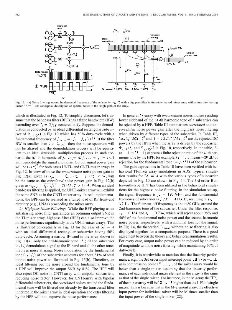
In general -array with uncorrelated noises, noises residinglower sideband of the -th harmonic tone of a subcarrier canbe rejected by a HPF. Table III summarizes correlated and un-correlated noise power gain after the highpass noise filteringwhen driven by different types of the subcarrier. In Table III,
and are the rejected DCpowers by the HPFs when the array is driven by the subcarrier
and in Fig. 10, respectively. In the table,( to ) expresses finite rejection ratio of the -th har-monic tone by theHPF: for example, means ofrejection for the fundamental tone of the subcarrier.The gain expressions in Table III have been verified with be-
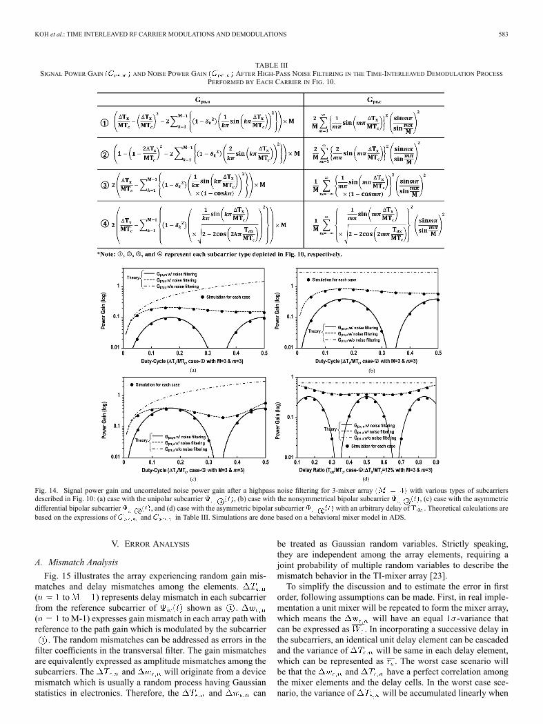
havioral TI-mixer array simulations in ADS. Typical simula-tion results for with the various types of subcarrierdepicted in Fig. 10 are shown in Fig. 14. The 3rd-order But-terworth-type HPF has been utilized in the behavioral simula-tions for the highpass noise filtering. In the simulation set-up,the signal frequency is , and the fundamentalfrequency of subcarrier is , resulting in
. The filter cut-off frequency is about 80 GHz, around the2nd-harmonic tone of the subcarrier. Under the filter response,
and , which will reject about 98% and46% of the fundamental noise power and the second-harmonicnoise power, respectively, with a minimal loss for the signal.In Fig. 14, the theoretical without noise filtering is alsodisplayed together for a comparison purpose. There is a goodagreement between the theory and behavioral simulation results.For every case, output noise power can be reduced by an orderof magnitude with the noise filtering, while maintaining 50% ofduty-cycle.Finally, it is worthwhile to mention that the linearity perfor-
mance, e.g., the 3rd order input intercept point orgain compression point , of the mixer array would bebetter than a single mixer, assuming that the linearity perfor-mance of each individual mixer element in the array is the sameas that of the single mixer. For instance, in the M-array theof themixer array will be higher than the IIP3 of singlemixer. This is because that in the M-element array, the effectiveinput power for individual mixer will be M times smaller thanthe input power of the single mixer [22].
KOH et al.: TIME INTERLEAVED RF CARRIER MODULATIONS AND DEMODULATIONS 583
TABLE IIISIGNAL POWER GAIN AND NOISE POWER GAIN AFTER HIGH-PASS NOISE FILTERING IN THE TIME-INTERLEAVED DEMODULATION PROCESS
PERFORMED BY EACH CARRIER IN FIG. 10.
Fig. 14. Signal power gain and uncorrelated noise power gain after a highpass noise filtering for 3-mixer array with various types of subcarriersdescribed in Fig. 10: (a) case with the unipolar subcarrier , (b) case with the nonsymmetrical bipolar subcarrier , (c) case with the asymmetricdifferential bipolar subcarrier , and (d) case with the asymmetric bipolar subcarrier with an arbitrary delay of . Theoretical calculations arebased on the expressions of and in Table III. Simulations are done based on a behavioral mixer model in ADS.
V. ERROR ANALYSIS
A. Mismatch Analysis
Fig. 15 illustrates the array experiencing random gain mis-matches and delay mismatches among the elements.( to ) represents delay mismatch in each subcarrierfrom the reference subcarrier of shown as .( to M-1) expresses gain mismatch in each array path withreference to the path gain which is modulated by the subcarrier. The random mismatches can be addressed as errors in the
filter coefficients in the transversal filter. The gain mismatchesare equivalently expressed as amplitude mismatches among thesubcarriers. The and will originate from a devicemismatch which is usually a random process having Gaussianstatistics in electronics. Therefore, the and can
be treated as Gaussian random variables. Strictly speaking,they are independent among the array elements, requiring ajoint probability of multiple random variables to describe themismatch behavior in the TI-mixer array [23].To simplify the discussion and to estimate the error in first
order, following assumptions can be made. First, in real imple-mentation a unit mixer will be repeated to form the mixer array,which means the will have an equal -variance thatcan be expressed as . In incorporating a successive delay inthe subcarriers, an identical unit delay element can be cascadedand the variance of will be same in each delay element,which can be represented as . The worst case scenario willbe that the and have a perfect correlation amongthe mixer elements and the delay cells. In the worst case sce-nario, the variance of will be accumulated linearly when

584 IEEE TRANSACTIONS ON CIRCUITS AND SYSTEMS—I: REGULAR PAPERS, VOL. 61, NO. 2, FEBRUARY 2014
Fig. 15. Time-interleaving process with errors from gain and delay mismatches among the array elements (the dotted rectangular pulses are ideal subcarriers).( to M-1) represents delay mismatch in each subcarrier with reference to the subcarrier of . ( to M-1) expresses gain mismatch
from in each array path with reference to the path modulated by the subcarrier of .
propagating the delay chain in Fig. 15. These assumptions arereflected in the transversal filter transfer function, in (21)at the bottom of the page, where the mismatch random variablesare incorporated in the complex weights in the first step and theneach random variable is approximated to its -variance. Note,
and can be treated as another Gaussian random variableswhich are common to each mixer and delay element. andwill have the same statistical properties as and ,
respectively.Usually the random mismatches are weak perturbations and
it will be a reasonable assumption that . This allowsin (21), resulting in the ap-
proximation of the magnitude response of the transversal filtertransfer function as
(22)
Fig. 16. Statistical mismatch simulation results of noise power gains in theTI-mixer arrays without noise filtering ( , duty-cycle of
): (a) UNTI-mixer array, and (b) CNTI-mixer array. Bar graphs are theresults fromMonte-Carlo simulations in ADS. -variance of and-variance of of (equivalently of phase-variance).
The output signal, , under the finite mismatches in thearray will be
(23)
(21)

KOH et al.: TIME INTERLEAVED RF CARRIER MODULATIONS AND DEMODULATIONS 585
Fig. 17. Contour plots of the noise factor, in (13), of UNTI-mixer arrays with (duty-cycle: 50%) under weight and delay mismatches: (a) noisefactor without noise filtering, (b) noise factor with an ideal bandpass noise filtering, and (c) noise factor with an ideal high-pass noise filtering (only fundamentaltone, , is rejected by an ideal HPF).
The signal power gain under the mismatches can befound by replacing with inTable II and Table III. The uncorrelated noise power gain underthe mismatches in UNTI-mixer arrays, corresponding to
in (18), can be given as
(24)
It should be noted that due to a lack of coherence amongthe noises in the UNTI-mixer arrays, the output noise powerand therefore is not dependent of phase mismatches, butproportional to the variance of the amplitude mismatches. Forthe CNTI-mixer arrays in Fig. 9(b), the correlated noise powergain under the mismatches, corresponding to in(19), will be approximated to (25), shown at the bottom of thepage.
B. Mismatch Behavioral Simulations
The mismatch models have been verified through Monte-Carlo (MC) mismatch simulations in ADS. Typical simulationresults are shown in Fig. 16 for the case of . The differen-tial subcarrier with 50% duty-cycle is utilized. It can beconfirmed from theMC simulations that the worst case error dis-tribution happens when and have a perfect corre-lation; and ( and 2) in Fig. 15 accumulates coher-ently across the delay chain as discussed. For a conservative es-timation, the Gaussian mismatch variables have been set as fol-lowing in the ADS MC simulations: two independent variablesof and are set as the same variable with of–variance; and where has
of –variance and has of –variance, respec-tively. Figs. 16(a) and 16(b) show probability distributions after2000 ADSMC runs for each case of UNTI- and CNTI-mixer ar-rays’, respectively. The theoretical distributions in Fig. 16 havebeen estimated using (24) and (25) in MATLAB statistical sim-ulations: –variances of and are 5% and 2%, re-spectively. There is a good agreement between the ADS MCsimulations and the theoretical estimations.For the UNTI-array under the weight and delay
mismatches, noise factor has been calculated basedon (23) and (24). Fig. 17 displays contour plots of the noisefactors which are well agreed with ADS behavioral simula-tion results. Fig. 17(a) show the noise factor without noise fil-tering. Figs. 17(b) and 17(c) are the cases with an ideal band-
(25)

586 IEEE TRANSACTIONS ON CIRCUITS AND SYSTEMS—I: REGULAR PAPERS, VOL. 61, NO. 2, FEBRUARY 2014
pass and highpass noise filtering, respectively. As expected, theTI-mixer array with uncorrelated noises exhibits a high sen-sitivity to the mismatches (reference: whenand without noise filtering, F(3) ). The band-pass and highpass noise filtering, however, reduce the sensi-tivity to the mismatches dramatically in the UNTI-mixer array.From ADS MC simulations, it can also be confirmed that inCNTI-mixer arrays sensitivity to mismatches can be reducedsubstantially by a bandpass noise filtering as well.
VI. CONCLUSIONS
This paper proposes a time-interleaved carrier modulationand demodulating technique. The present method is essentiallya mixer array technique relying on a parallel interleaving of aseries of modulated outputs in the time domain. The time-inter-leavedmixer array inherits a filtering function from a transversalfilter, and the time interleaving process is equivalent to a selec-tive filtering of a fundamental tone and its harmonics of carriersignals. A carrier waveform and duty-cycle play a critical rolein the noise performance of the arrays, and a comprehensivenoise analysis is presented for both correlated and uncorrelatednoises. Analytical mismatch models are provided and verifiedthrough ADS Monte-Carlo simulations. The time-interleavedarray technique will allow a high-speed in carrier modulationsand demodulations with a trade off a system complexity. It willbe a promising solution to realize high-frequency frequencymixing systems extending over millimeter and sub-millimeterwave regime under a limitation of active device speed.
REFERENCES
[1] “IEEE standard 802.15.3c, wireless medium access control (MAC) andphysical layer (PHY) specifications for high rate wireless personal areanetwork (WPANs),” Amendment 2: Millimeter-Wave Based Alterna-tive Physical Layer Extension, Ratified 12, Oct. 2009.
[2] A. Hirata, T. Kosugi, H. Takahashi, J. Takeuchi, H. Togo, M. Yaita, N.Kukutsu, K. Aihara, K. Murata, Y. Sato, T. Nagatsuma, and Y. Kado,“120-GHz-Band wireless link technologies for outdoor 10-Gbit/s datatransmission,” IEEE Trans. Microw. Theory Tech., vol. 60, no. 3, pp.881–895, Mar. 2012.
[3] J. Federici and L. Moeller, “Review of terahertz and subterahertz wire-less communications,” J. Appl. Phys., vol. 107, no. 11, p. 111101, Jun.2010.
[4] S. K. Reynolds, “A 60-GHz superheterodyne downconversion mixer insilicon-germanium bipolar technology,” IEEE J. Solid-State Circuits,vol. 39, no. 11, pp. 2065–2068, Nov. 2004.
[5] A. Parsa and B. Razavi, “A new transceiver architecture for the 60-GHzband,” IEEE J. Solid-State Circuits, vol. 44, no. 3, pp. 751–762, Mar.2009.
[6] F. Vecchi, S. Bozzola,M. Pozzoni, D. Guermandi, E. Temporiti,M. Re-possi, U. Decanis, and A. Mazzanti, “A wideband mm-Wave CMOSreceiver for Gb/s communications employing interstage coupled res-onators,” Proc. ISSCC Dig. Tech. Papers, pp. 220–221, Feb. 2010.
[7] B. R. Jackson and C. E. Saavedra, “A CMOS ku-band 4x subharmonicmixer,” IEEE J. Solid-State Circuits, vol. 43, no. 6, pp. 1351–1359, Jun.2008.
[8] H. Takahashi, T. Kosugi, A. Hirata, K. Murata, and N. Kukutsu, “10-Gbit/s quadrature phase-shift-keying modulator and demodulator for120-GHz-Band wireless links,” IEEE Trans. Microw. Theory Tech.,vol. 58, no. 12, pp. 4072–4078, Dec. 2010.
[9] J.-D. Park, S. Kang, and A. M. Niknejad, “A 0.38 THZ fully integratedtransceiver utilizing a quadrature push-push harmonic circuitry in sigebicmos,” IEEE J. Solid-State Circuits, vol. 47, no. 10, pp. 2344–2354,Oct. 2012.
[10] K. W. Kobayashi, A. K. Oki, L. T. Tran, J. C. Cowles, G.Gutierrez-Aitken, F. Yamada, T. R. Block, and D. C. Streit, “A108-GHz InP-HBT monolithic push-push VCO with low phase noiseand wide tuning bandwidth,” IEEE J. Solid-State Circuits, vol. 34, no.9, pp. 1225–1232, Sep. 1999.
[11] K. K. O, M. C. F. Chang, M. Shur, and W. Knap, “Sub-millimeterwave signal generation and detection in CMOS,” in Proc. MTT-S Int.Microw. Symp. Dig.,–188, Jun. 2009, p. 185.
[12] E. Seok, D. Shim, C. Mao, R. Han, S. Sankaran, C. Cao, W. Knap, andK. K. O, “Progress and challenges towards terahertz CMOS integratedcircuits,” IEEE J. Solid-State Circuits, vol. 45, no. 8, pp. 1554–1563,Aug. 2010.
[13] W. C. Black and D. A. Hodges, “Time interleaved converter arrays,”IEEE J. Solid-State Circuits, vol. SC-15, no. 12, pp. 1022–1029, Dec.1980.
[14] C. S. G. Conroy, D.W. Cline, and P. R. Gray, “An 8-b 85-MS/s parallelpipeline A/D converter in 1-mm CMOS,” IEEE J. Solid-State Circuits,vol. 28, 4, no. 4, pp. 447–454, Apr. 1993.
[15] D. Camarero, K. B. Kalaia, J.-F. Naviner, and P. Loumeau,“Mixed-signal clock-skew calibration technique for time-interleavedadcs,” IEEE Trans. Circuits Syst. I, Reg. Papers, vol. 55, no. 11, pp.3676–3687, Dec. 2008.
[16] A. V. Oppenheim, R. W. w. Schafer, and J. R. Buck, Discrete-TimeSignal Processing, 2nd ed ed. Upper Saddle River, NJ, USA: PrenticeHall, 1999.
[17] Advanced Design System (ADS). Santa Clara, CA, USA: AgilentTechnology Inc..
[18] L. W. Couch, Digital and Analog Communication Systems, 6 ed.Upper Saddle River, NJ, USA: Prentice Hall, 2000.
[19] K.-J. Koh, M.-Y. Park, C.-S. Kim, and H.-K. Yu, “Subharmonicallypumped CMOS frequency conversion (up and down) circuits for2-GHz WCDMA direct-conversion transceiver,” IEEE J. Solid-StateCircuits, vol. 39, no. 6, pp. 871–884, Jun. 2004.
[20] H.-C. Chen, T. Wang, H.-W. Chiu, Y.-C. Yang, T.-H. Kao, G.-W.Huang, and S.-S. Lu, “A 5-GHz-band CMOS receiver with low LOself-mixing front end,” IEEE Trans. Circuits Syst. I, Reg. Papers, vol.56, no. 4, pp. 705–713, Apr. 2009.
[21] S. He and C. E. Saavedra, “An Ultra-Low-Voltage and Low-PowerSubharmonic Downconverter Mixer,” IEEE Trans. Microw. TheoryTech., vol. 60, no. 2, pp. 311–317, Feb. 2012.
[22] R. V. Gatti, M. Dionigi, and R. Sorrentino, “Computation of gain, noisefigure, and third-order intercept of active array antenna,” IEEE Trans.Antennas Propagat., vol. 52, no. 11, pp. 3139–3142, Nov. 2004.
[23] P. Z. Peebles, Probability, Random Variables, and Random SignalPrinciples, 3 ed. New York, NY, USA: McGraw-Hill, 1993.
Kwang-Jin Koh (S’06–M’09) received the B.S. degree in electronic engi-neering (first-class honors) from Chung-Ang University, Seoul, Korea, in 1999,the M.S. degree in electrical engineering from the Korea Advanced Instituteof Science and Technology (KAIST), Daejeon, Korea, in 2001, and the Ph.D.degree in electrical and computer engineering from the University of Californiaat San Diego, La Jolla, CA, USA, in 2008.In November 2011, he joined the Electrical and Computer Engineering De-
partment, Virginia Polytechnic Institute and State University (Virginia Tech),Blacksburg, as an Assistant Professor.Dr. Koh was the recipient of the 2002 Best Paper Award of the IEEE Solid-
State Circuits Society and Electron Device Society, Seoul Chapter. His Ph.D.works on integrated phased arrays on silicon technologies have been reportedto the U.S. Pentagon as part of a Defense Advanced Research Projects Agency(DARPA) War Report as one of the major accomplishments of 2007. He wasalso the recipient of the 2010 Best Team of the Year Award of the TeledyneScientific Corporation (formerly the Rockwell Scientific Corporation), and 2012Virginia Tech ICTAS Junior Faculty Research Award.
Seyed Yahya Mortazavi (S’07) received the B.S. degree in electrical engi-neering from University of Tehran, Tehran, Iran, in 2003 and the M.S. degree inelectrical engineering from Tarbiat-Modares University, Tehran, Iran, in 2005.The M.S. research was on high-speed folding-Interpolating ADC design, andcontinued on wide-bandwidth high-resolution sigma-delta ADCs until 2010. Heis currently working toward the Ph.D. degree in electrical engineering at Vir-ginia Tech (VT), Blacksburg, VA, USA.His research interests include system and circuit design for RF and mm-Wave
integrated communication transceivers, and Imaging systems.
Sadia Afroz (S’10) received the B.S. degree in electrical engineering fromBangladesh University of Engineering and Technology, Bangladesh, in 2011.She is currently working toward the Ph.D. degree at Virginia Tech, Blacksburg,VA, USA.Her research was on high-speed Ultra wideband Inter and intra-chip wireless
communication system until 2011. Her current research interests include designofmillimeter-wave circuits, wireless transceiver and Phased-array architectures.
Copyright © 2022 FDOKUMEN