
design, analysis and implementation of an interleaved pfc ...
134
DOKUZ EYLÜL UNIVERSITY GRADUATE SCHOOL OF NATURAL AND APPLIED SCIENCES DESIGN, ANALYSIS AND IMPLEMENTATION OF AN INTERLEAVED PFC BOOST DC/DC CONVERTER FOR AN LCD TV POWER SUPPLY by Mustafa Murat KARAPARTAL June, 2011 İZMİR
-
Upload
khangminh22 -
Category
Documents
-
view
5 -
download
0
Transcript of design, analysis and implementation of an interleaved pfc ...

DOKUZ EYLÜL UNIVERSITY
GRADUATE SCHOOL OF NATURAL AND APPLIED
SCIENCES
DESIGN, ANALYSIS AND IMPLEMENTATION
OF AN INTERLEAVED PFC BOOST DC/DC
CONVERTER FOR AN LCD TV POWER SUPPLY
by
Mustafa Murat KARAPARTAL
June, 2011
İZMİR

DESIGN, ANALYSIS AND IMPLEMENTATION
OF AN INTERLEAVED PFC BOOST DC/DC
CONVERTER FOR AN LCD TV POWER SUPPLY
A Thesis Submitted to the
Graduate School of Natural And Applied Sciences of Dokuz Eylül University
In Partial Fulfillment of the Requirements for the Degree of Master of Science
in Electrical and Electronics Engineering
by
Mustafa Murat KARAPARTAL
June, 2011
İZMİR

ii
M.Sc THESIS EXAMINATION RESULT FORM
We have read the thesis entitled ―DESIGN, ANALYSIS AND
IMPLEMENTATION OF AN INTERLEAVED PFC BOOST DC/DC
CONVERTER FOR AN LCD TV POWER SUPPLY‖ completed by MUSTAFA
MURAT KARAPARTAL under supervision of ASST. PROF. DR.ÖZGE ŞAHİN and
we certify that in our opinion it is fully adequate, in scope and in quality, as a thesis for
the degree of Master of Science.

iii
ACKNOWLEDGMENTS
I would like to express my sincerest thanks to Asst. Prof Dr. Özge Şahin for her
guidance, support and encouragements throughout the preparation of this thesis.
I express my deepest gratitude to my parents, for their encouragements throughout
my education life. Their love, care and encouragement has given me a great inner
strength to success. This work is dedicated to them.
I also want to thank to my administrator and colleagues in VESTEL High-End R&D
for their support and help during my thesis research.
Mustafa Murat KARAPARTAL

iv
DESIGN, ANALYSIS AND IMPLEMENTATION OF AN INTERLEAVED
PFC BOOST DC/DC CONVERTER FOR AN LCD TV POWER SUPPLY
ABSTRACT
Nowadays, because of the increasing use of semiconductors and power
electronics devices, current harmonics effects on the electrical systems have become
intolerable. Therefore, it has become essential to reduce these harmonic currents,
which affect the energy system quality negatively. This also affects the shape of
current to achieve a good power factor. According to the EU standard for harmonic
reduction IEC 61000-3-2, an active power factor control stage should be utilized if
the power consumed by an LCD-TV is above 75 W. The largest power consuming
sub-system of an LCD TV is the backlight driving circuit. Plasma technology was
the first historical solution; however, Cold Cathode Fluorescents Lamps (CCFL) with
LCD panels previously used for note books rapidly took the leadership. These
florescent lamps came into use with only medium sized screen TVs, but they are now
used in every size. The LED backlight solution for LCD TVs is started to become a
very popular way to allow small depth design with slim cabinets, particularly with
Edge LED solutions. This thesis studies the design stages of this technology in
accordance with the slim converter board.
The focus of this thesis is the design and implementation of such a high
performance switched–mode power supply. The work involves the design and
implementation of an interleaved Power Factor Correction (PFC) for high
performance and small size, the controller design and implementation of boost
DC/DC converter. With Frequency Clamped Critical Conduction Mode (FCCrM)
PFC, the overall system efficiency is increased since the active power consumption is
decreased.
The design procedure, including the design of the circuit components and the
control loop, is implemented and the results are verified by a 150W prototype
converter. The interleaved dual Boundary Conduction Mode (BCM) PFC controller
operates two parallel-connected boost power converters 180 degree out of phase,

v
extending the maximum practical power level of this control technique from 200-
300W up to 800W. The converter designed in this work can be applied to CCFL or
LED backlight LCD TV application since converter circuit driving the backlight unit
is placed on a different board. Flexibility and adaptation for different backlight
inverter units are satisfied by this application.
Keywords: CCFL (Cold Cathode Fluorescent Lamp), PFC (Power Factor
Correction), FCCrM (Frequency Critical Conduction Mode), Boost Converter,
Interleaved PFC.

vi
LCD TV İÇİN AYRIK MOD GÜÇ FAKTÖRÜ DÜZENLEYİCİSİ
YÜKSELTİCİ TİPTE DA/DA ÇEVİRİCİ DEVRE TASARIMI
DOĞRULAMASI VE İNCELENMESİ
ÖZ
Günümüzde yarıiletken elemanların ve buna bağlı olarak güç elektroniği
cihazlarının kullanımının artmasıyla birlikte harmonik akımların şebekeye etkileri
yadsınamaz hale gelmiştir. Şebekeden çekilen enerjinin kalitesizleşmesine neden
olan bu akımların azaltılması ve akımın şekillendirilmesi üzerine çalışmalar yaparak
güç faktörü değerinin uygun seviyelere çekilmesi bir gereksinim olmuştur. LCD TV
lerde geçerli olan ve AB standartlarına göre düzenlenen IEC-61000-3-2’ ye göre,
eğer tasarlanan TV evrensel olarak satışa sunulacaksa ve 75W’ın üzerinde çıkış
gücüne sahip ise aktif güç faktörü düzenleyicisi kullanması zorunludur. Tarihte ilk
olarak büyük güçler tüketen plazma teknolojisi ile ortaya çıkan bu aktif güç faktörü
düzenlemesi, düşük güç tüketimleri ile hızla plazmanın yerini alan LCD TV’ lerde de
uygulanmaktadır. Son yıllarda ortaya çıkan çeşitli LED arka plan uygulamaları,
incelikleri sayesinde LCD’lere göre daha ince kabin yapısında kullanılmaktadır.Bu
çalışmamızda tasarım aşamaları anlatılan çevirici kartın tasarımı ince kabin yapısına
uygun olarak tasarlanmıştır.
Bu tez çalışmamızın esas amacı yüksek performanslı anahtarlamalı güç kaynağı
tasarlanması ve uygulanmasıdır. Bu çalışmada yüksek verimli, küçük boyutlarda ve
ayrık mod yapısına sahip güç faktörü düzenleyicisi ile yükseltici çevirici topolojisine
uygun DA/DA çevirici birleştirilerek tasarlanmış ve uygulaması gerçekleştirilmiştir.
Tasarlanan bu dönüştürücüde Frekans Kritik İletim Modu (FCCrM) PFC ve
yükseltici çeviricili denetleyici topolojileri kullanılmaktadır. Bu yapı sayesinde aktif
güç tüketimi azalmasına sağlar iken genel sistem verimliliğini de arttırmaktadır.
Bu tasarım için hazırlanan prototip kartın deneysel olarak 150W desteklediği
doğrulanmıştır. Bu uygulamada kullanılan 180 derece faz farkı ile çalışan ayrık

vii
yapısı sayesinde 200-300W’ lık güç seviyelerinden 800W’ lık güç seviyelerine
ulaşabilen tasarım yapılmasına olanak sağlamaktadır. Tasarlanan bu kart
CCFL(Cold Cathode Fluorasent Lamp) ya da LED aydınlatmalar için
kullanılabilmektedir. Bu çalışmada tasarlamış olduğumuz çeviricinin yanı sıra ayrı
bir kartta tasarlanan evirici sayesinde büyük bir esneklik kazandırılarak tüm CCFL
ve LED arka plan aydınlatmalarında kullanılabilmesi sağlanmıştır.
Anahtar kelimeler: CCFL (Soğuk katot florasan lamba), PFC (Güç faktörü
düzenleyici), FCCrM (Frekans Kritik İletim Modu), Yükseltici Çevirici, Ayrık Güç
Faktörü Düzenleyici.

viii
CONTENT
Page
M.Sc. THESIS EXAMINATION RESULT FORM ..................................................ii
ACKNOWLEGMENTS ........................................................................................ iii
ABSTRACT ........................................................................................................... iv
ÖZ .......................................................................................................................... vi
CHAPTER ONE – INTRODUCTION ................................................................ .1
1.1 Description .................................................................................................... 1
1.2 Literature Overview ........................................................................................ 2
1.3 Thesis Outline ................................................................................................ 6
CHAPTER TWO–POWER FACTOR CORRECTION ..................................... .7
2.1 Background ................................................................................................... 7
2.2 Definitions ..................................................................................................... 9
2.3 Harmonics and Current Emission Standards ................................................. 12
2.4 Power Factor Correction Approaches and Comparisons ................................ 18
2.4.1 PFC Methods............................................................................................ 18
2.4.2 Passive Approach .................................................................................... 19
2.4.2.1 Single Phase Full-Wave Rectifier ...................................................... 21
2.4.2.2 Passive Power Factor Correction Methods ......................................... 25
2.4.2.2.1 LC Filter Methods ........................................................................ 25
2.4.2.2.2 Series Connected Parallel Resonant Filter .................................... 26
2.4.2.3 Limitations of Passive PFC Circuits ................................................... 28
2.4.3 Active PFC .............................................................................................. 29

2.4.3.1 Active Two-Stage Approach .............................................................. 30
2.4.3.2 Active Single-Stage Approach ........................................................... 32
2.4.4 Comparison of PFC Solutions .................................................................. 33
CHAPTER THREE–AVERAGE CURRENT CONTROL MODE OF BOOST
CONVERTER ...................................................................................................... 35
3.1 Description ................................................................................................... 35
3.2 Power Balance Analysis Of Circuit .............................................................. 37
3.3 Input Voltage Feed Forward ......................................................................... 41
3.4 Control Loop Design .................................................................................... 47
3.4.1 Current Loop Design .............................................................................. 48
3.4.2 Voltage Loop Design .............................................................................. 53
3.5 Simulation of Average Current Control Mode of Boost Converter ................ 56
3.6 Hardware Implementation of Current Control Mode of Boost Converter ...... 61
3.6.1 Functional Description of Power Circuit ................................................. 61
3.6.2 Functional Description of Control Circuit ............................................... 63
3.7 Design of Average Current Control Mode of Boost Converter ...................... 64
3.8 Experimental Results .................................................................................... 69
3.9 Summary ...................................................................................................... 72
CHAPTER THREE–AVERAGE CURRENT CONTROL MODE OF BOOST
CONVERTER ...................................................................................................... 73
4.1 Introduction ................................................................................................. 73
4.2 Operation of Critical Conduction Mode ........................................................ 74
4.3 Analysis of Switching Characteristic Critical Conduction Mode ................... 77
4.4 Simulation of Characteristic Critical Conduction Mode PFC ........................ 81
4.5 Operation of Interleaved PFC System .......................................................... 85

4.6 Interleaved PFC Technique Analysis of Switching Characteristic ................. 87
4.7 Simulation of Interleaved PFC ...................................................................... 91
4.8 Hardware Implementation of Interleaved PFC .............................................. 94
4.8.1 Functional Description of Power Circuit ................................................. 94
4.8.2 Functional Description of Control Circuit ............................................... 95
4.9 Design of Interleaved PFC Circuit .............................................................. 97
4.10 Experimental Results ................................................................................ 101
4.11 Summary .................................................................................................. 106
CHAPTER FIVE– CONCLUSION AND FUTURE WORK ........................... 107
REFERENCES ................................................................................................... 109
APPENDIX A – ................................................................................................... 112
APPENDIX B – ................................................................................................... 118

1
CHAPTER ONE
INTRODUCTION
1.1 Description
The usage of electronic equipments is increasing rapidly in the daily life
according to consumer or industrial needs. All these electronic equipments have
power supplies that obtain required energy from utility grid. These electronic
systems generally use one or more switched mode power supplies (SMPS) that draw
a non-sinusoidal current. This causes current and voltage distortions that affect other
equipments connected to the same power grid, thus, lowering the capability of the
power source. In order to overcome these problems, new standards have been
developed for limiting the harmonic content of the input current. Manufacturers
should find solutions for meeting the requirements of these standards.
Most of the power supplies consist of AC/DC converter stages based on diode or
thyristor rectifier circuits. Conventionally, these stages consist of a diode rectifier
with an output capacitor. These rectifier circuits constitute a major cause of mains
harmonic distortion. Line-frequency diode rectifiers convert AC voltage into DC
output voltage in an uncontrolled way. For low power applications (such as PCs,
TVs, home appliances, etc…) single-phase diode rectifiers are chosen owing to low
cost and simple structure. For high power applications (such as industrial equipments
and motor drives) three-phase diode or thyristor rectifiers are used. A typical offline
SMPS contains full-wave bridge rectifier with a large smoothing capacitor. This
combination is one of the easiest and lowest cost solutions for AC/DC conversion.
This input rectifier with capacitive filter draws non-sinusoidal input current from
utility.
In the general usage, different load groups are supplied by different phases. If one
of the phases is loaded with nonlinear loads, unbalanced currents flow through the
neutral line of star configuration.

2
These unbalanced currents cause heating and power loss in the conductors and
voltage distortion and electromagnetic compatibility (EMC) problems occur.
Moreover the harmonic content of this pulsating current causes additional losses and
dielectric stresses in capacitors and cables, increasing currents in windings of
rotating machinery and transformers and noise emissions in many products, and
bringing about early failure of fuses and other safety components. Harmonics can
affect other devices that are connected to the same system.
In order to reduce these harmonic polluting effects, international standards such as
IEC 61000-3-2 have been developed for limiting harmonic currents. The
International Electro technical Commission (IEC) sets limits for harmonics in the
current of small single-phase or three-phase loads, less than 16 A per phase, in
Electromagnetic compatibility (EMC) - Part 3-2: Limits - Limits for harmonic
current emissions (IEC 61000-3-2) [1]. The circuit classifications and harmonic
limits are given in this standard. The power supply manufacturers use different
solutions for complying with the specifications. The techniques for reduction of
current harmonics are called Power Factor Correction (PFC) solutions. The aim of
PFC is providing a resistive load behavior of all power supplies.
1.2 Literature Overview
As the use of energy is increasing, the requirements for the quality of the supplied
electrical energy are more tighten. This means that power electronic converters must
be used to convert the input voltage to a precisely regulated DC voltage to the load.
Regulated DC power supplies are needed for most analog and digital electronic
systems. Most power supplies are designed to meet regulated output, isolation and
multiple outputs (Mohan, et al. 2005).
Regulation means that the output voltage must be held constant within a
specified tolerance for changes within a specified range in the input voltage and the
output loading.

3
Isolation is needed when the output is required to be electrically isolated from the
input. They might be multiple outputs that may differ in their voltage and current
ratings. Such outputs can be isolated from each other.
Beside these requirements, common goals are to reduce power supply size and
weight and improve their efficiency. Traditionally, linear power supplies have been
used. However, advances in semiconductor technology have lead to switching power
supplies, which are smaller and much more efficient compared to linear power
supplies. But the cost comparison between linear and switching power supplies
depends on the power rating (Dixon, 1988).
The number of SMPS and other power electronics appliances are increasing.
SMPS are needed to convert electrical energy from AC to DC. SMPS are used as a
replacement of the linear power supplies when higher efficiency, smaller size or
lighter weight is required. Motors, electronic power supplies and fluorescent lighting
consume the majority of power in the world and each of these would benefit from
power factor correction. In the middle of 1990s, many of the countries of the world
have adopted requirements for power factor correction for new products marketed
within their borders.
PFC is becoming a very important field in power electronic world. Adding more
generating capacity to the world’s electrical companies due to higher demand
recently is very costly and would consume additional resources. One method of using
extra power capacity is to use the AC power more efficiently through the broad use
of PFC (Brown, 1994).
Most of research in PFC are based on reduction of harmonic contents in the line
current. In passive PFC, only passive elements are used to repair the shape of input
line current. Obviously, the output voltage cannot be controlled.

4
In active PFC circuit, an active semiconductor device is used together with passive
elements to shape the input current and also controlling the output voltage (Ross,
1997).
In another study by Woo-Young Choi and Bong-Hwan Kwon (Choi& Kwon,
2008) an efficient PFC for plasma display panels (PDPs) is presented to reduce
harmonic currents and power consumption. A high-efficient interleaved boost
converter is proposed, which can reduce the conduction losses and diode reverse-
recovery problems in the continuous-conduction-mode operation. A zero-current
switching (ZCS) condition is obtained to solve the reverse-recovery problems of the
output diodes. In addition, a control strategy is suggested for the use of the proposed
converter in a practical design. A high power factor can be achieved without sensing
the input voltage. The analysis of the proposed converter and its design
considerations are presented in detail.
In another study by Jong C. Wang and Hon-Ji.Chen (Wang & Chen,2001) , two
current sharing control schemes based on average current mode control is proposed
for interleaved PFC converter. The boost inductor current of each phases of
interleaved PFC must be sensed to achieve current sharing and power limiting. To
meet this requirement, it is proposed a current transformers current sense skill which
achieve current sharing and also can improve current harmonic distortion during high
line operation.
In another study by K. I. Hwu and C. F. Chuang (Hwu & Chuang, 2006), a two-
phase boost converter based on interleaved control is presented to upgrade the output
power as well as to improve the power factor. Such interleaved control is realized via
the proposed control rule and implemented by logic circuits.Some simulation and
experimental results are provided to demonstrate the effectiveness of the proposed
control strategy.

5
In another study by Dodi Garinto (Garinto, 2007), a very unique boost converter
system with a combination of interleaving and zero-ripple techniques for PFC is
proposed. The converter allows clean power in the universal AC line (90 V to 265 V)
and compliance with any standards or regulations.
The converter is designed in Discontinuous Conduction Mode (DCM) operation to
reduce the system complexity and to eliminate diode reverse recovery loss. This can
remove electromagnetic interfrance (EMI) filter without sacrificing the input current
harmonics. Consequently, high density PFC converter with low cost can be achieved.
In this study, first of all, general information about harmonics, which causes
measurement errors, overheating of motor windings and switches etc., and most
common harmonic sources are given. After that, relation between harmonics and
power factor is mentioned and converters, one of the harmonic sources,are explained
and analyzed. Passive and active PFC techniquesare studied.
Finally, the design procedure which is including the design of the circuit
components and the control loop is implemented and the results are verified by a
150W prototype converter. The interleaved dual Boundary Conduction Mode (BCM)
PFC controller operates two parallel-connected boost power converters 180º out of
phase and converter is designed for CCFL or LED backlight LCD TV application
since converter circuit driving the backlight unit is placed on a different board.
Flexibility and adaptation for different backlight inverter units are satisfied by this
application.

6
1.3 Thesis Outline
This thesis is organized in five chapters. The first chapter covers the literature
rewiew about basics of the PFC, harmonic current standards and general solutions for
PFC.
The second chapter deals with popular passive and active power factor correction
methods.
Different techniques are analyzed and theoretical analysis is verified by experimental
results are given. Furthermore, designing passive and active solutions to comply with
harmonic current standards are discussed.
In the third chapter Average Current Mode Controlled,which is the main subject of
this mode control with boost type converter is implemented by using NCP1379 IC.
This case is analyzed then theoretical and experimental results are given.
In the fourth chapter Critical Conduction Mode control and interleaved PFC are
examined. The circuit is implemented by NCP1631 IC which is a special control
technique that includes interleaved structure. This special case is analyzed,and its
experimental verification is presented.
Finally, the last chapter covers the advantages and disadvantages of the PFC
which are evaluated throughout the thesis.

7
CHAPTER TWO
POWER FACTOR CORRECTION
2.1 Backround
After achieving alternative energy sources, fossil fuels or the roads that traverse a
long and happy to spend time causing homes, our factories allow us to generate
revenue by producing, altering our view of the world by sending rockets into space
cockpits, computers, televisions, large and small human found on most machines,
and briefly devices that use electricity and electricity can be found in every place.
Most of the electricity we use is in the form of alternating current. Alternating
current power systems for the distribution of a given voltage and a fixed frequency
sinusoidal current and voltage waveforms must be complete. However, the linear and
nonlinear reactive elements, the use of elements that is unable to follow each other in
the network's current and voltage waveforms and sine current wave form of phase
shift leads to corruption. Sinusoidal harmonic components of the mountain, the way
the event occurs in the form of deviation is evaluated. Power factor leading to decline
in these situations, especially for the active power consumed means more capacity.
( Scillic, (2004), ―Power Factor Correction Handbook‖.)
A typical offline SMPS contains full-wave bridge rectifier with a large smoothing
capacitor. This combination is one of the easiest and lowest cost solutions for AC-
DC conversion. This input rectifier with capacitive filter draws non sinusoidal input
current from utility. The pulsating current waveform is rich of harmonics (N. Mohan,
T. Udeland, & W. Robbins, Power Electronics: Converters, Applications and
Design, 2nd ed. New York: Wiley, 1995). A typical single-phase rectifier with
capacitive smoothing and its output voltage and input current waveforms are shown
in Figure 2.1 and Figure 2.2.

8
Figure 2.1 Single-phase rectifier with capacitive smoothing.
Figure 2.2 Waveforms for single-phase rectifier with capacitive smoothing.
Passive methods, AC and DC coil and capacitor parties are provided to improve
by adding the current wave shape. In addition, the serial-parallel resonant band stop
filter, harmonic gripper approaches are frequently used. Passive approaches,
simplicity, reliability, lack of advantages such as high-frequency loss, while the
heavy and bulky material employed, the dynamic responses have disadvantages such
as poor and lack of output voltage regulation. Active filters are suffering in the non-
linear elements in the form of sine wave is not the inverse of the current system by
injecting a sinusoidal current withdrawal offer from the network. Active filters,
although they are expensive to conduct more than one filter for harmonic frequency
in the system due to changes in the superior to passive filters.

9
Active PFC techniques are examined in low frequency and high frequency
operations. These circuits, used in the topology, control the shape, the coil,
depending on criteria such as current status, follows the input current and voltage
with the output values and allows to shift the phase between current and voltage,
current, wave shape, preventing deterioration.(Dorf, C., Richard, Ed., (2000), ―The
Electrical Engineering Handbook‖.)
2.2 Definitions
Power factor, the "real" operating power, and apparent power, can be found by
proportion. Real power (W), apparent power (VA) and reactive power (VAr) are
shown as the edges of a right triangle. Thus, W is the real power, apparent power VA
multiplied by the cosine of the angle ø between the two powers in this section
(Cos ø), including the results of the "power factor," gives the known rate.
Figure 2.3 Power factor correction vectors.
PF has range between 0 and 1 and is defined as the ratio of the real power to the
apparent power.
ø
(2.1)

10
The real power is defined as the product of the fundamental voltage and
fundamental current and the phase displacement between the two.
ø (2.2)
where V1,rms, I1,rms are the rms values of the fundamental line current and the
fundamental line voltage, respectively, and is the phase shift between line current
and line voltage.
The apparent power is the product of rms voltage and rms current :
(2.3)
In a linear load system, the power factor depends on phase difference between V rms
and Irms. Then, the power factor can be expressed as:
ø
= ø (2.4)
It is shown that in the case of both sinusoidal voltage and current waveform
systems with no phase difference between fundamental component of the current and
voltage achieve unity power factor. This situation appears in resistive load circuits.
In a nonlinear load system with distorted current waveform, the rms values of the
input current and the fundamental frequency component of the input current are not
the same. The various harmonic components of the current appear as distorted power
on the line. Then the power factor expression in the case of stable line voltage can be
written as:
ø = ( 2.5)
Where
is the distortion factor and ø is
the displacement factor.

11
Distortion factor describes harmonic content of the current. It shows the difference
between fundamental component of the current and actual waveform.
Total Harmonic Distortion (THD) shows the ratio of the rms value of the
waveform (not including the fundamental component) to the rms value of the
fundamental component.
(2.6)
Then distortion factor can be written by using THD definition in Eq. (2.6)
(2.7)
In Figure 2.4, it can be seen that the different voltage and current waveforms result in
different PF and THD due to distortion factor and displacement factor.
Figure 2.4 Different current and voltage waveforms of single phase rectifier

12
2.3 Harmonics and Current Emission Standards
Harmonic is not a new subject in. This issue were to come across as a problem
for a long time. Communication systems, especially the first times in a way quite
often these effects came from the agenda.
Magnetizing currents of transformers in these systems, the open-line telephone
networks, inductive interference caused by harmonic currents. It is impossible to
speak he was so Ventures. Investigation and had brought along on this issue,
studying required. Finally, the transformer magnetizing currents brought to the rules
designed to minimize and filter it was possible. Harmonics on power system
components and load a number of undesirable effects. These are short-and long-term
effects. Short-term effects are usually associated with the most obvious ones and
over-voltage surge. On the other hand, long-term effects are usually inconspicuous
and increased resistance depends on the losses and voltage stresses. Short-term
adverse affect sensitive loads will cause the initiation. Computer controlled, some
loads are sensitive to voltage fluctuations. Voltage fluctuation can be problematic,
while 5% had no cases out of over 10% of the transformer to overheat and cause
unwanted triggers. (R. Redl, P.Tenti & V.Wyk, Power electronics polluting effects,
IEEE Spectrum, Volume 34, Issue 5, May 1997)
Most electrical equipments are designed to operate under ideal sinusoidal
environment. In the case of a harmonically polluted system the power line loses its
ideal characteristic. The practical problems that may arise from excessive harmonic
levels are:
Harmonic currents flowing in the supply network generate additional energy
losses and cause distortion of supply voltage.

13
Higher frequency harmonic currents cause power losses (copper and iron
losses) which result in an increase in the heating of elements. Equipment
ratings must take the presence of harmonics into account. The higher rated
neutral conductor is required to carry the added high frequency currents.
Distorted waveforms result in poor power factor.
Interference to equipment which is sensitive to voltage waveform
Damage to power factor correction capacitors. Malfunction of ripple control
and other mains signaling systems, protective relays and, possibly, in other
control systems.
Additional losses in capacitors and rotating machines.
Additional acoustic noise from motors and other apparatus, reducing the
efficiency of motors.
The diode bridge input circuit in a single-phase AC drive is the same as used
in a very wide range of electronic equipment such as personal computers and
domestic appliances. All of these cause similar current harmonics.
Their effect is cumulative if they are all connected to the same low voltage (e.g.
230V) supply system. This means that to estimate the total harmonic current in an
installation of single-phase units, the harmonics have to be added directly. The power
system is designed for predefined current values and all components belonging to
this system have standard ratings and protection elements. Low power factor devices
that draw higher current from the mains reduce the efficient power supplied by the
mains. This means that low power nonlinear loads are reflected to the mains side
with higher power ratings.

14
Since the power line system is designed for fixed values, available power at the
load side is decreased because of low power factor loads.
Harmonic currents in the AC distribution network require higher current carrying
capacity that results in extra cost and power losses. This increasing capacity first
affects the device and then the electric utility.
The wire sizes and ratings should be increased. In residences and offices, energy
meters cannot measure the reactive power that affects dissipative circuit elements so
the user is not directly penalized in terms of utility costs for the reactive component
of the power. In ideal case the voltage at the utility side is assumed to be an ideal
sinusoidal waveform. But actually AC source has small source impedance.
Highly distorted current loads affect power line, resulting in distorting AC source
voltage. The movement of the source voltage towards to non sinusoidal waveform
can affect other equipments which are connected to the same power system.( R.
Redl, Electromagnetic Environmental Impact of Power Electronics Equipment,
Proceedings of the IEEE, Vol 89, No:6, June 2001)
The harmonic polluting effects of conventional AC rectification must be limited
and this is done in accordance with the standards of electricity utility network. To
maintain power system quality, compliance requirements for current harmonic
distortion are being enforced by national and international bodies .( IEC61000-3-2,
Electromagnetic Compatibility (EMC)—Part 3: Limits—Section 2: Limits for
Harmonic Current Emissions (Equipment Input Current <16A per Phase),). The EN
61000-3-2 standard defines measurement requirements, ac power source
requirements and limits for testing the harmonic current emissions of electronic and
electrical equipment.
The purpose of EN 61000-3-2 is limitation of harmonic currents injected to the
power system. After some changes, this standard applies to any equipment with rated
current up to 16 A RMS per phase for 50-Hz, 230-V single-phase systems or 400-V

15
three-phase mains network. There are 4 different classes in the EN 61000-3-2 that
have different limit values. This classification is made according to:
Number of pieces of equipment in use (how many are being used by
consumers)
Duration of use (number of hours in operation)
Simultaneity of use (the same types of equipment used on the same time
frame)
Power consumption
Harmonics spectrum, including phase (how clean or distorted is the current
drawn by the equipment)
There are no limits for:
Equipment with input power P > 75 W.
Professional equipment with input power P > 1 kW.
Symmetrical controlled heating elements with input power P > 200 W.
Independent dimming devices for light bulb
Non-public networks.
Medical equipment
Equipment for rated voltages less than 230 VAC (limit not yet been
considered).

16
Equipment can be grouped into 4 classes based on the above criteria as evaluated
by the IEC committee members: Class A, B, C and D. They have several limitations
of odd and even harmonics. In here I gave Class D table because of my LCD power
supply application belong to this class.( TS EN 61000-3-2, Elektromanyetik
Uyumluluk (EMU)-Bölüm 3-2: Sınır Degerler-Harmonik Akım Emisyonları İçin Sınır
Değerler (Faz Basına Donanım Giriş Akımı <16A), TSE, MART 2003 )
Table 2.1 Class D absolute maximum harmonic limits
Harmonic Order
(n)
75W<P<600W
Maximum permissible current
(A)
P>600W
Maximum
permissible current
(A)
3 3,4 2,30
5 1,9 1,14
7 1,0 0,77
9 0,5 0,40
11 0,35 0,33
13 0,296 0,25
15≤n≤39 3,85/n 2,25/n
Class D limits are very strict to meet as seen in Table 2.4. These limits depend on
the equipments’ power rating and apply to equipments that are connected to the
utility network for a significant part of its life cycle, resulting in great impact on the
power supply network. PCs and TVs are examples of such equipment.
The current limits for class D are expressed in terms of mA per Watt of the power
consumed. Low-power equipment has very low absolute limits of harmonic current.
All rectifier based power supplies that are directly connected to the mains are
generally classified as Class A or Class D. Such converters that have highly distorted
current waveform and used more frequently are classified as in Class D.

17
Table 2.2 IEC 61000-3-2 changes
IEC61000-3-2:1995
EDITION 1.0
IEC61000-3-2:2001
EDITION 2.1
IEC61000-3-2:2005
EDITION 3.0
CLASS D
DEFINITION
Special waveform envelope
(75W to 600W)
TV, PC and Monitor (75W to
600W)
TV, PC and Monitor (75 to
100W)
MEASUREMENT
METHODS
Steady and transitory Transitory only Transitory
only
Transitory only
MEASUREMENT
METHODS
16 cycles
(320/267ms@50/60Hz)
200 ms (10/12 cycles@50/60
HZ) (16
cycles permitted through
2004)
200 ms (10/12 cycles@50/60
HZ)
DATA
MANIPULATION
Transitory only All data must be smoothed
using the1.5s first order filter
All data must be smoothed
using the 1.5s first order filter
PASS/FAIL FOR
INDIVIDUAL
HARMONICS
Every window result <150%
of limit of test time >100%
permitted
Every window result <150%
of limit 10% of test time
>100% permitted
Every window result <150%
of limit 10% of test time
>100%
CLASS A
RELAXATION*
No special provision No special provision
<200 time of limit only IF
>150% for 10% of test time
AND average
ODD HARMONICS
21-39*
No special provision
Provision for POHC
calculation
permitting the average of
some
individual harmonics to
>100%
Provision for POHC
calculation
permitting the average of
some
individual harmonics to
>100%
CLASS C&D LIMITS
Proportional to measured
power
(Class D) or current & PF
,Class C
Allows manufacturer o
specify test power or current
level provided it is within
±10% of the measured value
Allows manufacturer o
specify test power or current
level provided it is within
±10% of the measured value
TEST/OBSERVATION
Not specially defined but to
find
the max. harmonics emission
Specified to be significantly
long
enough to acquire ±5%
repeatability. If to long select
the 2.5 min. max.
Specified to be significantly
long
enough to acquire ±5%
repeatability.

18
2.4 Power Factor Correction Approaches and Comparisons
2.4.1 Power Factor Correction Methods
The need for Power Factor Correction brings a lot of new PFC methods and
applications. The most important issue is finding optimum PFC solution according to
needed application. There are several survey papers in order to help to find the best
solution for power factor correction.( Fernandez, A., Sebastian, J., Hernando,
M.M.,Villegas, P.& Garcia, J. ―Helpful hints to select a power-factor-correction
solution for low- and medium-power single222 phase power supplies‖ Industrial
Electronics, IEEE Transactions on Volume 52,Issue 1, Feb. 2005 Page(s): 46 – 55 )
The Power Factor Correction methods can be classified according to following
specifications:
System level classification (passive, active)
Number of stages (single stage, two stage)
Circuit based classification (isolated, non isolated)
Type of power stages (buck, boost, fly back etc…)
Waveform based classification (sinusoidal, non-sinusoidal)
Control methods (current mode, voltage mode)
The other aspects (power level, cost, complexity, etc…)
Generally, two PFC approaches are commonly used in current power supply
products with high power features, i.e., passive approach and active PFC approach.
Each one has its merits and limitations and applicable field.

19
Passive PFC approaches are used in low-power, low-cost applications. Generally,
in this approach, an L-C filter is inserted between the AC mains line and the input
port of the diode rectifier of AC-to-DC converter. Passive PFC method is simple and
low cost but has bulky size and heavy weight and low power factor. Active solutions
are used at high power levels with high PF and low harmonic distortion. We can
classify active PFC methods as two stage and single stage by considering number of
conversion stages.( Gracia O., Jose A.,Prieto R. & Uceda J, ―Single Phase Power
Factor Correction:A Survey‖, IEEE Transactions on Power Electronics,Voi
18,No3,May 2003,pp-749-755. )
The most commonly used active approach is the two-stage approach with higher
quality. Generally two-stage PFC systems consist of a pre-regulator cascaded with a
DC/DC converter. In the first stage, generally called as pre-regulator, a non-isolated
boost converter has the role of power factor correction. This front end PFC stage
converter generally operates for low harmonic input current and intermediate dc bus
voltage. The second stage operates for required dc voltage level with higher
bandwidth.
The second stage generally has isolation two-stage systems have higher quality
with higher PF and low harmonic distortion. However, the two-stage approach
causes an increase in the total system cost and manufacturing complexity. Especially
in low-power applications, two-stage solutions have higher cost. For reducing system
cost and component count, single stage solutions have been introduced. In the single-
stage systems, PFC, isolation and dc voltage regulation are performed in one stage
with lower component number.
2.4.2 Passive Approach
In the passive PFC approaches, passive elements are used to improve the power
quality of the power circuit. Passive elements like inductors and capacitors are placed
at the inputs or outputs of the diode bridge rectifier in order to improve current
waveform. Generally, output voltage is not controlled.

20
Passive PFC systems are dependent on the power system and has low power
factor. Generally, line frequency LC filters are used as a passive solution. The simple
passive filter with LC components is shown in Figure 2.5. The passive components
improve current conduction angle and reduce THD of the input current. Line
frequency inductance can be placed either on the DC or AC side of the rectifier.(
Sharifipour, B. Huang, J. S., Liao, P., Huber L. & Jovanovic, M. M.
―Manufacturing and cost analysis of power-factor-correction circuits,‖ IEEE
Applied Power Electronics Conf. (APEC) Proc., 1997, pp.490-494 )
Due to its simplicity, the passive LC filter could be a high-efficiency and low-cost
PFC solution in order to meet the IEC 61000-3-2 specifications. Passive power factor
correction method meets Class-A/D equipment specifications up to 300 W, at a much
lower cost than a comparable switch mode power supply (SMPS) employing active
PFC techniques. The passive PFC technique is most suitable for applications with a
narrow line voltage range. However, it can be also employed in power supplies
operating in the universal line-voltage range (90 - 265 VAC).
Figure 2.5 Simple passive PFC circuit.
The major advantages of the passive PFC technique are higher efficiency, low
complexity, and lower cost. The lower component count and absence of active
switches and control circuitry, translate into higher reliability and somewhat smaller
size. Also, when compared to active circuits, the losses of the passive filters are
lower. However, the passive filters have heavy and bulky low frequency passive
elements like line frequency inductance. The other disadvantage of the passive filters
is the unregulated varying dc bus voltage that becomes the input to the
DC/DCconverter.

21
This varying input voltage has effects on the efficiency of the DC/DC converter.
The power factor of passive PFC circuits is around 0.60 - 0.70 and, needs
arrangement of component ratings when operated under universal line voltage
conditions.
Generally a large DC bus capacitance is needed in the output of the rectifier for
better hold-up time and low ripple output voltage. Meeting the Class-A harmonic
requirements can be easily done by passive filters for low-power applications but
class-D applications require passive filters of a bigger size. This bigger size brings
higher cost and physically higher dimensions.
2.4.2.1 Single Phase Full-Wave Rectifier
Generally, most of the AC-DC power supplies consist of a full bridge diode
rectifier as an input stage. A bulk capacitor is installed to the output of the rectifier to
regulate the output DC voltage. As mentioned in the previous chapter, the load of
the rectifier requires low ripple supply voltage. The large capacitor supplies low
ripple DC output voltage but this shortens considerably the input current’s
conduction duration.( Redl,R. & Balogh,L. ―Power-Factor Correction in Bridge and
Voltage-Doubler Rectifier Circuits with Inductors and Capacitors‖
APEC´95,pp.466-472) Short current conduction interval results in a narrow pulsed
current waveform. This current waveform is rich in harmonics that have negative
effects on the main side of the system as explained in Chapter 1.
A typical single-phase full bridge diode rectifier is shown in Figure 2.6 with
supply impedance and large output capacitor filter.

22
Figure 2.6 Typical single-phase rectifier.
The short conduction times for diode rectifier causes short current conduction
interval because the diodes conduct only when the input voltage is greater than the
output capacitor voltage.
This period is short when the output capacitor is fully charged. The general
current and voltage waveforms for a single-phase rectifier with large output capacitor
are given in Figure 2.6.
Figure 2.7 Current and voltage waveforms.

23
The output capacitor defines the shape and the amplitude of the input line current.
Large value of output capacitor provides low ripple output voltage, however input
current has small conduction period, because diode rectifier conducts only when
input voltage is higher than output capacitor voltage. In this condition, input current
has significant harmonics and system has lower power factor. Input current distortion
can be reduced by using a smaller output capacitor. With smaller capacitance filter
output voltage increases and the current conduction interval widens.
This method is very easy to implement and cheaper than other solutions, but the
load is directly affected by increased output voltage ripple. In the SMPS applications,
generally a DC/DC converter is inserted after diode bridge rectifier. This DC/DC
converter is designed assuming that the input voltage is stable and well regulated. In
the case of small output filter capacitance, it is hard to implement a constant power
DC/DC converter with variable input voltage.
Figure 2.8 Simulated input voltage and current waveforms with capacitive filter.

24
This solution can be applied if the load accepts a largely pulsating DC supply
voltage and it is used, for example, in some hand held tools.( Redl,R. and ELFI S.A.,
―An Economical Single-Phase Power- Factor- Corrected Rectifier: Topology,
Operation, Extensions, and Design For Compliance‖ PEC´98, pp.454-460 )A single-
phase diode bridge rectifier with capacitive filter is simulated for different values of
output capacitor filter. The filter capacitor is selected for two different values, 0.5
μF/W and 2.35 μF/W. A 200-W constant power loaded single-phase rectifier is
simulated by SIMPLORER simulation tool. The input current waveforms and output
voltage waveforms are shown in Figures 2.8 and 2.9.
Figure 2.9 Simulated output voltage ripple with capacitive filter.
It can be seen from these figures that, when output capacitor is reduced, input
current conduction interval increases, however output voltage ripple increases also.
Usually, this increased output ripple is unwanted in the switch mode power supply
applications.

25
2.4.2.2 Passive Power Factor Correction Methods
Passive power factor correction is implemented by connecting passive elements to
the diode bridge rectifier. There are various combinations of passive elements for
power factor correction with different circuit topologies .Before the harmonic
limiting standards, the investigators have designed passive solutions for better PF
and efficiency because there were no limits for current harmonics. After the IEC
61000-3-2 standard was accepted, the designers had to change the previous solutions
or design new circuits obeying the standards. In this thesis, three of the various
passive power factor correction techniques are investigated in detail and simulation
and experimental results are verified. These are
LC filter
Series Connected Parallel Resonant Filter
2.4.2.2.1 LC Filter Method . The simplest passive solution to comply with the
EN 61000-3-2 standard is LC filter method. Passive LC filter power factor correction
can be done by connecting one inductor to the capacitive filtered diode bridge
rectifier. Filter inductor can be placed either on the AC side or DC side. When the
inductor is connected to the AC side, current harmonic distortion can be reduced by
large inductance but voltage drop (reduced output power) in the inductor will be
large. By connecting the filter inductor to the DC side, output power will be
independent from filter inductance but harmonic limiting capability will be lower
than inductor in the AC side.
In this section, the design of single-phase diode bridge rectifier with output LC
filter complying with the EN 61000-3-2 standard is given. In the design the
following criteria are considered.
Standard compliance
Maximum Power Factor
Minimum Line Current Harmonic
Cost and Size

26
Optimum solutions satisfying the above criteria are given. A general single-phase
diode rectifier with LC filter is given in Figure 2.10. While designing LC filter, input
voltage is assumed as a zero-impedance source and diode rectifier is assumed
lossless (ideal diodes). The output power and output voltage are assumed constant
(large output capacitor).
Figure 2.10 Normalized single phase rectifier.
The circuit can be analyzed easily by normalization procedure The operation
modes of the circuit and the current waveforms depending on the output filter
inductance can be evaluated using normalization methods. The circuit variables are
converted to the normalized values by using reference values. In the rectifier system
three main reference values are utilized. These are voltage, current and the time
references.
2.4.2.2.2 Series Connected Parallel Resonant Filter. Power factor improvement via
reducing input current harmonics for a single-phase rectifier with a capacitive output
filter can alternatively be done by using resonant filters. There are different resonant
network based passive solutions. Two main resonant solutions are:
Series connected series resonant band pass filter tuned at line frequency
Series connected parallel resonant band stop filter tuned at third harmonic

27
In this section, the series connected parallel resonant filter shown in Figure 2.11
is investigated and verified experimentally, since it requires lower values of reactive
elements compared to other solutions.
Figure 2.11 Series connected parallel resonant filter.
A single-phase full bridge rectifier with capacitive filter draws higher harmonic
currents from line. The most significant harmonic is the third harmonic. If this one is
reduced or cancelled, the rectifier will have higher power factor due to lower input
RMS current and lower THD. The series connected parallel resonant filter is tuned to
3rd harmonic and, generally, called as a third harmonic filter. The proposed filter in
Figure 2.11 has an input LC parallel resonant tank tuned at 3rd harmonic. The
inductance and capacitance values of the resonant tank are selected to behave as an
infinite (theoretically) impedance to the third harmonic input current component. So
the system will eliminate the third harmonic content of the input current. This
condition brings lower input rms current value with lower THD. So the system will
have higher power factor and efficiency. The nth order equivalent impedance of the
resonant tank can be defined by:
(2.8)

28
where XLr, is the impedance of the input resonant inductor Lr at fundamental
frequency, XCr, is the impedance of the input resonant capacitor Cr at fundamental
frequency. The third harmonic impedance from (2.8) becomes infinity (theoretically)
when;
(2.9)
Or
(2.10)
Where
The single-phase rectifier is assumed lossless with no voltage drop in the diodes.
The output voltage is assumed ripple free with large output capacitor. The line
voltage is assumed sinusoidal and the load is assumed to be a constant power load.
The values of the reactive elements in the resonant filters are selected for higher
power factor defined in the section 2.4.2.
2.4.2.3 Limitations of Passive PFC Circuits. The simplicity, reliability,
insensitivity to noise and surges and the no generation of any high-frequency EMI
offered by passive power factor circuits are of significant usefulness. However, the
bulky size of these filters, their poor dynamic response, complexity and high cost, the
lack of voltage regulation and their sensitivity to line frequency, limits their use to
below 200-W applications. Moreover, even though line current harmonics are
reduced, the fundamental component may show an excessive phase shift resulting in
reduction in power factor.

29
2.4.3 Active PFC
Active power factor correction techniques are used for high quality rectifiers.
Active PFC circuits shape the input current into a sinusoidal form in phase with line
voltage. Besides they provide a regulated dc output voltage. These circuits have
resistor behaviors at the line side of the converter. Generally power factor of active
PFC circuits is close to unity with lower input current THD around 3 %. Active PFC
circuits have small size but these systems have higher manufacturing cost and
complexity. A DC/DC converter operates as an active shaper in the range of 10 kHz
to hundreds of kHz. Active switches are used in conjunction with reactive elements
in order to increase the effectiveness of the line current shaping and to obtain
controllable output voltage. Higher operation frequency provides smaller size of
reactive components such as inductors.( Basu,S.& Undeland, T.M., Fellow, IEEE.
―PFC Strategies in light of EN 61000-3-2‖. (EPE-PEMC 2004 Conference in Riga,
LATVIA, 1- 3 September 2004) )
Traditionally, the implementation of power factor correction circuits has been
accomplished by using analog controllers. Active PFC can achieve high power factor
controlled by analog circuits using several methods. Various analog PFC ICs are
available in the electronic markets, which are manufactured by TI/Unitrode,
Fairchild, Onsemi and others manufacturers. Complete list of the available PFC ICs
and the specifications will be given in the appendix. Analog control is simple and
low cost. Continuous operation and higher operating dynamics make the analog
control suitable. But analog control has higher element count. Analog control
methods are also application dependent. It is hard to adopt a new operating condition
when a change is needed. The system should be redesigned from scratch. Recently,
power supplies are implemented by digital controllers. Recent developments in
digital control techniques and low cost digital control ICs make digital control
optimum for power supply applications. It is not easy to maintain the available
control methods with digital controllers, because these control methods require high
speed calculations and high-speed analog to digital conversions.

30
The operating frequency and the speed of the digital control devices are limited.
New control strategies have been developed suitable for digital operations. Digital
systems need lower component count then analog systems, so size of the digital
implementations are smaller. Digital systems are flexible and can be operated under
different conditions by software based control strategies. The single-phase active
PFC techniques can be divided into two categories: the two stage approach and the
single-stage approach shown in Figure 2.12.
Figure 2.12 a) Two-stage PFC b) Single-stage PFC.
2.4.3.1 Active Two-Stage Approach
The most popular scheme for power factor corrected AC-DC power supplies is
the two-stage approach. In this approach, two converters share power factor
correction and dc voltage regulation roles. The front-end converter operates as power
factor corrector while shaping line current, therefore achieving unity input power
factor.

31
The PFC front-end stage operates as DC/DC converter with regulating output
voltage and provides isolation if needed. Both converters are controlled separately.
Independent PFC controller provides sinusoidal input current with intermediate
regulated output voltage. Second DC/DC controller provides tight regulated output
voltage with high bandwidth. The first PFC stage can be a boost, buck/boost or fly
back or can assume any other power converter topology. Generally, the boost type
topology shown in Figure 2.13 is so far the most popular configuration. It provides
input-current shaping with low bandwidth control. With the boost-type topology, the
system has some advantages
such as:
The inductor current and the input current have the same waveform so it is
easy to apply current mode control over boost inductor.
The system has lower EMI with the help of series boost inductor with the ac
line.
Input current can be continuous or discontinuous.
The switching element such as MOSFET or IGBT is parallel to the power
line. The system has better efficiency and low noise. But it requires extra
protection to input- output short circuit and start-up spikes.
Figure 2.13 Boost type active PFC.

32
The boost-type PFC can be operated in continuous-conduction-mode (CCM),
discontinuous-conduction-mode (DCM), variable-frequency critical (boundary)
conduction mode.
There are several control methods for high power and low current THD. This
thesis is concerned with the control methods of boost type active PFC which are
implemented experimentally. Popular control methods are explained and the results
are given by computer simulations and experimentally.
In summary, the active two-stage PFC converter has good input power factor and
can be used in wide ranges of input voltage and output power. However, the two-
stage approach suffers from an increased circuit complexity since it requires two
switches and two controllers with associated circuitry. It is very undesirable for low-
power supplies used in consumer electronic products. In the high power applications,
the two-stage system seems the best solution.
2.4.3.2 Active Single-Stage Approach
If the aim for designing PFC solution for an available AC-DC converter is only
meeting the harmonic standards with lower harmonic quality and lower
manufacturing cost, the single-stage systems are suitable methods for power factor
correction. In the single-stage approach, PFC and dc voltage regulation are made by
one controller. Most single-stage topologies combine the input current shaping with
the DC/DC down-conversion in a single stage. Single-stage solution with single
switch seems to be the right solution at lower power levels (< 200 W), because
reduced component count and cost of the PFC stage provide a cheaper solution than
two stage systems. The only controller is the DC/DC controller, which focuses on the
tight regulation of the output voltage. The input power factor of a single-stage
converter is not unity, but its input current harmonics are small enough to meet the
specifications, such as the IEC 61000-3-2 class D. Generally, the active single-stage
approach offers a performance (THD and PF) which is better than the corresponding
performance of the passive solution, but not as good as that of the active two-stage
approach.

33
The primary advantages of this approach are lower part count and cost than two-
stage PFC topologies. With these technologies, the PF is typically >0.75 and THD is
typically <80%. The major deficiency of any single-stage circuit is that the voltage of
the internal energy-storage (bulk) capacitor varies with the line voltage and load
current. Because of all process is done by single controller, the system has
higher control complexity.
2.4.4 Comparison of PFC Solutions
The above mentioned three solutions for power factor correction have advantages
over the other according to application and usage. A summary of the three methods is
given below:
Passive harmonic line current reduction
Simple and not complex circuit
Large and bulky low frequency reactive elements
Less costly than active PFC
Redesign needed for wider operation range
Active harmonic line current reduction
High power factor (close to unity) and lower THD of line current
Higher cost and component count
Complex to control and design
Increased noise such as EMI, RFI
In Figure 2.14, the input voltage and current waveforms are shown for three
operations.
Figure 2.14 Waveforms without/with PFC ( a) Without PFC b) passive PFC c) active PFC.)

34
According to the above evaluation, the designer can choose best solution for
power factor correction considering selection criteria, especially power level for
single phase power conversion. If the output power is less than 200 W, single-stage
PFC and the passive PFC are valid options. Above 200 W, the conventional two-
stage PFC seems to be the best choice. If the purpose is to obtain a sinusoidal line
current, the classical two-stage approach is the best option mainly if universal line
voltage operation is required. Passive solutions are adequate in low power for
simplicity. Single-stage solutions are a good option to meet the low frequency
harmonic regulations in low power applications with low cost a comparison chart is
given in Table 2.3.
Table 2.3 Comparison table of three solutions
PASSIVE
ACTIVE
TWO-STAGE
ACTIVE
SINGLE -STAGE
THD High Low Medium
POWER
FACTOR
Low High Medium
EFFICIENCY High Medium Low
SIZE Medium Large Small
WEIGHT Very High Low Low
BULK CAP
VOLTAGE
Varies Constant Varies
CONTROL Simple Complex Simple
COMPONENT
COUNT
Very Low High Medium
POWER RANGE < 200-300W Any < 200-300W
DESIGN
DIFFICULTY
Low Medium High

35
CHAPTER THREE
AVERAGE CURRENT CONTROL MODE OF BOOST CONVERTER
3.1 Description of Average Current Control Mode of Boost Converter
This chapter deals with the average current mode control of a single-phase boost
PFC (Dixon, L. H. High Power Factor Preregulators for Off-Line Power Supplies,
Unitrode Power Supply Design Seminar Manual SEM600, 1988) A detailed
theoretical analysis of the average current mode control of PFC will be reviewed and
supported by hardware implementation. The PFC IC, NCP1379, will be used to
implement this strategy and design and functional description of the circuit will be
explained.
The block diagram of the PFC circuit is given in Figure 3.1. The circuit consists
of a single-phase rectifier with a cascaded boost converter that provides active wave
shaping of the input current and regulation of the output voltage. Active power factor
correction is achieved by the power switch duty cycle.
The switching frequency of the converter is higher than line frequency such as
100 kHz for 50-Hz power system. When the switch is turned on, the boost inductor
stores energy from input. At the same time, the output rectifier diode is reverse
biased and the load is supplied by the output capacitor. When the switch is turned
off, the output capacitor and the load are supplied by the input over the boost
inductance.
The average current controlled PFC system has two control loops. The system
has fast inner current loop that enables the input current to follow the reference
current. The reference current is multiplication of the reference shape and reference
amplitude.

36
Figure 3.1 Average current mode control of PFC
The reference current gets the sinusoidal shape of the input voltage. The
amplitude of the reference current is defined by the outer voltage loop. The system
has a low bandwidth outer voltage loop which programs the required input current
reference magnitude according to the power consumption of the load. This function
is done by using an output voltage regulator control circuit.
The inner current loop operates in average current mode that controls the average
input current. The input current IL(t) is compared with Iref per switching cycle and
passed through an error amplifier that produces a control voltage vc. This control
voltage is than compared with constant frequency saw tooth waveform to produce
required duty cycle of the power switch. The saw tooth waveform defines the
switching frequency. The bandwidth of the current loop is very high such as decade
of the switching frequency. The higher bandwidth current controller allows the input
current to follow reference current with lower noise.

37
The output loop has an output voltage controller for regulating the output voltage.
The output voltage v0(t) is compared with reference voltage vref. The voltage
controller consists of a voltage error amplifier that produces error voltage VAOUT
according to the variations in the output voltage. This error voltage VAOUT programs
the current reference magnitude.High power factor operation is obtained by average
current mode control. The inputcurrent follows the sinusoidal reference. Finally, the
input current and the voltage of the PFC system will have the same waveform and
phase.
3.2 Power Balance Analysis of the Circuit
In a converter system, the output voltage should be regulated to the required level
bya voltage controller in a closed system. Generally, the output voltage is constant in
DC/DC converter. The constant dc output voltage v0 (t) = V is obtained by a wide
bandwidth voltage controller. If the converter has constant load, the instantaneous
load power is also constant.
(3.1)
Generally, the load of a PFC system is a DC/DC converter. This load draws constant
power. But the instantaneous input power pac(t) is not constant.
(3.2)
where vg(t) and ig(t) are input ac voltage and current, respectively. The instantaneous
input power can be written according to resistor emulation concept by using the
peak input voltage value.
(3.3)
The input power varies with time. The output capacitor provides power balance to
maintain the input-output power balance. The difference between input and output
power flows through output electrolytic capacitor.

38
So the power on the output capacitor can be written:
(3.4)
where vc(t) is output capacitor voltage. When pac(t) > p0(t) than energy flows into
output capacitor and vc(t) increases. When pac(t) < p0(t), the capacitor voltage vc(t)
decreases. So the capacitor voltage increases and decreases for power balance action.
The changes of input power and capacitor voltage are shown in Figure 3.2.
Figure 3.2 Variation on the capacitor voltage.
The output voltage regulation is achieved by comparing the actual output
capacitor voltage with reference voltage. The error voltage amplifier provides
enough amplitude information for current reference for power balance operation. A
block diagram of the outer voltage loop is shown in Figure 3.3.
Figure 3.3 Multiplier based control.

39
(3.5)
where cos(2wt) is second harmonic voltage ripple due to second
harmonic current component of the output current. This ripple voltage lags the ripple
current by 90°. It is assumed that reference voltage vref is equal to the DC component
of vc (t).
(3.6)
So the error voltage verr is equal to only second harmonic component of the capacitor
voltage.
cos (2wt) (3.7)
Assume that the voltage controller compensator has wide bandwidth so 2nd harmonic
component feeds back through the voltage error amplifier. A general equation for the
output of the voltage error amplifier VAOUT can be written as:
cos(2wt) (3.8)
In a multiplier based system shown in Figure 3.3, the current reference Iref is
obtained by the multiplication of the current reference waveform IAC with the output
of the voltage error amplifier VAOUT.
(3.9)
It is known that waveform component IAC of the current reference evaluated from the
rectified input voltage has only sinusoidal waveform information. So a general
equation for this component IAC can be written as:
sin (wt) (3.10)

40
So the reference current Iref can be written as:
sin(wt) cos(2wt) (3.11)
The equation can then be rearranged as:
(3.12)
It is shown in the equation above that, the 2nd harmonic distortion on the output
voltage distorts the input current reference Iref. The second order harmonic
component of the output voltage adds a 3rd harmonic component to reference current
with a half magnitude of the second harmonic component.
So in average current mode controlled PFC system, the input current is forced to
follow input current reference. If a distortion occurs in reference current also actual
input current distorts. This 3rd harmonic distortion in the input current lower PF.
The solution for lowering this distortion is to configure the output voltage error
amplifier to block the second harmonic component of the output voltage. This is
done by using an error amplifier that has lower bandwidth. The bandwidth of this
controller should be lower than 2nd order frequency of the line voltage such as 20 Hz.
But lower bandwidth means slower response. The slower transient response makes
the dc regulation worse. A designer should consider the trade-off between lower
THD and faster transient response.( Dixon, L. H. Optimizing the Design of High
Power Factor Switching Preregulator, Unitrode Power Supply Design Seminar
Manual SEM700, 1990) Generally, the load of PFC system is a second DC/DC
converter that has a tight output voltage regulation. So the designer should choose
better input current waveform. But if the second DC/DC converter needs a narrow
range input voltage, the designer should consider transient response. There are some
strategies to get better voltage loop response as given in literature. But the solution is
inside the application. Detailed analyses of the voltage loop are given in the control
circuit description section.
41
3.3 Input Voltage Feed-Forward
It was mentioned that a power factor pre-regulator is generally the first stage of a
two-stage power supply system. The second stage is the load of the PFC stage and
composed of a constant power DC/DC converter. So PFC stage has a constant power
load that does not change with the input rms voltage. The PFC stage maintains a
fairly constant output voltage and the load draws constant power regardless of the
variations of output voltage of the PFC stage. In a high efficient PFC circuit, if the
output load power is constant, the input power drawn from line does not change with
rms line voltage. So if there is a change in input rms voltage, the input rms current
should change inversely proportional to the rms input voltage. But it is known that
the reference current is directly proportional to the input line voltage in an average
current controlled PFC in Figure 3.1. There is a conflict between power balance and
control circuit when operated in universal line (90-270 Vac).
Basically, the current reference Iref is obtained by multiplication of the input
voltage waveform information signal IAC and the output voltage error signal VAOUT.
It is assumed that the PFC circuit operates with 120Vac input voltage VIN with
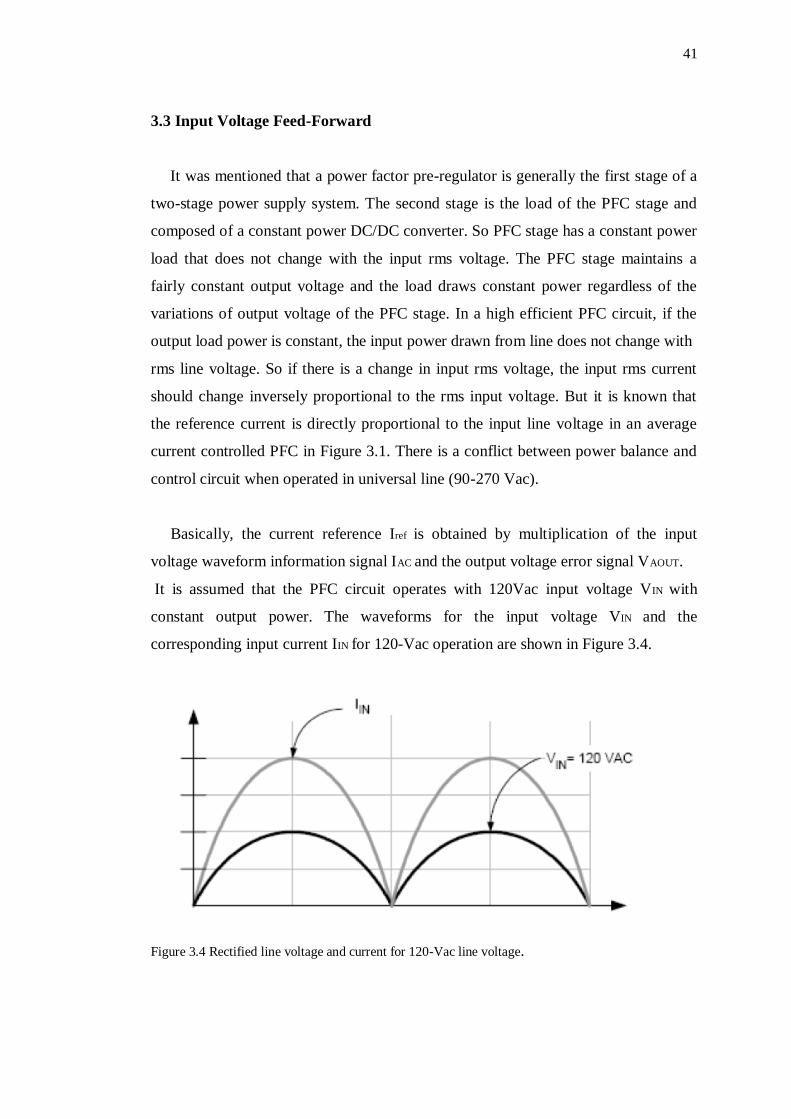
constant output power. The waveforms for the input voltage VIN and the
corresponding input current IIN for 120-Vac operation are shown in Figure 3.4.
Figure 3.4 Rectified line voltage and current for 120-Vac line voltage.

42
The multiplier inputs IAC and VAOUT are shown in Figure 3.5 for 120-Vac operation.
Figure 3.5 Multiplier inputs IAC and VAOUT at 120-Vac line voltage.
Assume PFC is operating in universal input line and the input voltage VIN is
doubled from 120 Vac to 240 Vac. When input voltage VIN is doubled, input current
IIN should be halved in order to maintain constant power to the load. The waveforms
for the input voltage VIN and the corresponding input current IIN for doubled input
voltage operation are shown in Figure 3.6.
Figure 3.6 Rectified line voltage and current for 240-Vac line voltage.
The multiplier input IAC is directly proportional to the input voltage VIN. When
VIN is doubled, IAC is also doubled. The multiplier output Iref is current reference for
the actual input current IIN, has to halve, that can only be accomplished by reducing
voltage error amplifier voltage VAOUT by factor four.

43
The multiplier inputs IAC andVAOUT are shown in Figure 3.7 for 240-Vac operation.
Figure 3.7 Multiplier inputs IAC andV AOUT at 240-Vac line voltage.
So the optimum PFC performance is obtained by fast response voltage loop
controller in a universal power line operation. But the voltage loop limitation
problem has already been mentioned in the previous section. The outer voltage loop
controller should have small bandwidth in order to remove the second harmonic
component in the voltage feedback circuit. The output of the voltage feedback
controller should be constant in the half cycle of line frequency. If the voltage loop
controller has small bandwidth, the control circuit should be independent of the line
voltage in order to solve the problems due to the variations of the line voltage. The
solution is called as input voltage feed-forward.( Williams, J. B. "Design of
Feedback Loop in Unity Power Factor AC to DC Converter", PESC Conf. Proc.,
1989, pp. 959-967.)
The input voltage feed-forward makes the control circuit independent from the
input line voltage by modifying the multiplier concept. A new signal proportional to
the input voltage is added to the input of the multiplier. This signal is called as
feedforward and represented by VFF. The feed-forward signal VFF is squared and
inversed so VFF signal becomes as a divider factor (1/ VFF2). The modified average
control system with input voltage feed-forward is shown in Figure 3.8.

44
Figure 3.8 Block diagram of the average current PFC with feed-forward.
The new control strategy provides independent operation of voltage error
controller to the input voltage variations. In fact, the output voltage error amplifier is
only dependent on the output power. If the input voltage doubles, the doubled IAC
signal is divided by factor four by the new input feed-forward signal (1/ VFF2). So the
new current reference Iref is equal to half of the original signal before doubling line
voltage without any change in VAOUT. The new equation for the current reference Iref
can be written as:
(3.13)
The control system with input voltage feed-forward has all the capabilities for
high power factor application for universal input line. The current reference Iref is the
combination of IAC that has the waveform of the rectified input voltage and VAOUT
that is proportional to the output power. And it is mentioned that the output voltage
loop has smaller crossover frequency and the output VAOUT is constant during line
cycle. The other input IAC of multiplier is derived by a resistor dividing circuit of
rectified input voltage so IAC varies during line cycle. The third input of the multiplier
is the feed-forward signal VFF. Now the design of the feed-forward application will
be considered.

45
Since the feed-forward signal VFF consists of the rms input voltage information,
this signal can be obtained by resistor divider connected to the dc side of bridge
rectifier. Since the rectified input voltage has large 2nd harmonic component, the
feed-forward signal VFF should be filtered.
This averaging network is done by low pass filter. The first order averaging low
pass filter for the feed-forward signal VFF is shown in Figure 3.9. The capacitor
averages the rectified input voltage waveform and reduces the 2nd harmonic ripple.
The time constant of the filter network defines the amount of the 2nd harmonic ripple
in the input of the multiplier.
If time constant (RC) is smaller, the feed-forward compensation network will have a
faster response but 2nd harmonic ripple will be high.
Figure 3.9 First order input voltage feed-forward sensing scheme
This will reduce power factor. If the time constant is larger, there will be too
much feed-forward delay resulting in worse transient response such as higher
overshoots. The transient response can be increased with lower 2nd order ripple
distortion and can be achieved by a second order low pass filter as shown in Figure
3.10.

46
Figure 3.10 Second order input voltage feed-forward sensing scheme.
A second order low pass filter network can increase the complexity and
manufacturing cost. In fact, input voltage does not change instantaneously so fast
transient response is not really required.
Some new generation IC’s combines the evaluation of IAC and VFF .The feed-
forward signal VFF is obtained by mirroring IAC signal so a second resistor divider
circuit is removed. The new voltage feed-forward sensing schemes is shown in
Figure 3.11.
The amount of ripple on the feed-forward signal VFF distorts the input current. The
low pass filter attenuates most of 2nd order harmonic but some 2nd order harmonic
exists in feed-forward signal. The distortion is the same as the voltage loop distortion
explained in the previous section. 2nd harmonic ripple in the feed-forward signal
causes 3rd harmonic distortion in the line current. But the amplitude of the 3rd
harmonic distortion is equal to the 2nd harmonic ripple amplitude in the feed-forward
signal due to squaring process. On the other hand, distortions due to feed-forward
sensing scheme and voltage loop have the same phase and are multiplied as the
inputs of the multiplier.( Noon, J.P. & Dalal, D. Practical design issues for PFC
circuits, IEEE APEC 1997.)

47
Figure 3.11 First order input voltage feed-forward sensing scheme
3.4 Control Loop Design
In average current controlled PFC application, there are two control loops that
provide a sinusoidal input current in phase with input voltage.
The design of the voltage and current loops has significant affects in the system
performance, such as amount of THD and PF. The control circuit has inner current
loop that ensures the form of Iref based on the input voltage. The outer voltage loop
determines the amplitude of the current reference Iref based on the output voltage
feedback. The outer voltage loop adjusts the inductor current amplitude to bring the
output voltage to the reference voltage. The block diagram of the control loops for an
average current controlled PFC is shown in Figure 3.12.
Figure 3.12 PFC control loops.
The control loops are designed separately. The inner current loop has higher
bandwidth. The voltage loop has lower bandwidth due to distortion factors.

48
3.4.1 Current Loop Design
Inner current loop of average current controlled PFC needs inductor current
sensing. The sensed current via shunt resistor or current transformer is compared
with reference current that is output of the multiplier. The error between actual
inductor current and the reference current is amplified with a properly designed
current compensator. The output of the compensator is compared with a saw tooth
waveform to produce required duty cycle for the PFC boost operation.
The main feature of the average current control is the presence of the current error
amplifier (compensator) that provides controlling the average inductor current. The
inner current loop block diagram can be built with the combination of the current
sensing circuit, current error amplifier, PWM generator and power stage of the PFC
boost converter as shown in Figure 3.13.
Figure 3.13 PFC current loop.
The inner current loop has large bandwidth around one decade of the switching
frequency. A small signal model of the inner current loop is needed to design a
proper compensator with optimum performance and stability. A Laplace domain of
the inner current loop is shown in the figure 3.14.
Figure 3.14 Laplace domain block-schema of the current loop

49
The open loop transfer function of the inner current loop can be written as:
Ti(s)=Fm(s)RsGp(s)Gc(s) (3.14)
where Fm (s) is modulator gain of the PFC controller, Rs is the current sensing
resistor, Gp(s) is power stage transfer function, and Gc (s) is current compensator
transfer function.
The transfer function of the modulator is dependent on the peak value of the ramp
voltage in the PWM controller. So the transfer function of the modulator can be
written as:
(3.15)
where VSE is equal to the peak-to-peak amplitude of the external ramp. A small
signal model of the power converter is needed for the design of the current
compensator.
The averaged small-signal model of the converter defines the dependence of the
average input current on the duty cycle. When the converter operates at steady-state,
the output voltage has small variations around a steady-state component. The output
voltage can be expressed as:
TS =V+ vˆ( (t) (3.16)
The averaged small signal model of the PFC boost converter with dynamically
changed variables is shown in Figure 3.15. The linearization and the perturbation
procedure are used for completing the small signal model of the converter.

50
Figure 3.15 Linearized model of the PFC boost converter.
The average inductor voltage of the PFC boost converter can be written as:
İ
TS – d
ı(t)( V+ vˆ((t)) (3.17)
The nonlinear term dV(t) + vˆ(t) in the equation (3.17) is much smaller than the
linear term d1(t)V . Therefore, this nonlinear term can be discarded. The average
inductor voltage can be obtained as:
İ
TS – d
ı(t)V (3.18)
The equivalent circuit given in Figure 3.15 is used to obtain control-to-input transfer
function by using the equation (3.18) and found by setting the independent inputs to
zero and solving the inductor current Ig. The simplified small signal transfer function
of the PFC boost converter Gp(s) is written as
Gp(s)= İ
)=
(3.19)
The open loop transfer function of the current loop without the current compensator
Gid(s) can be written as the combination of the power stage, sensing resistor and
PWM modulator.

51
Gid(s)= Fm(s)RsGp(s) (3.20)
The complete open loop transfer function of the current loop with current
compensator Ti(s) is
Ti(s)= Gid(s) Gc(s) (3.21)
The current compensator is designed according to the behavior of the converter
without the current compensator. The current compensator should be designed for
optimal performance and stability for overall current loop. The Bode blot of the
Gid(s) is a good reference for the design of the current compensator. The Bode plot of
the Gid(s) with arbitrary chosen values (L = 1mH, V0 = 400V, VSE = 4V) is shown in
Figure 3.16.
Figure 3.16 Magnitude and phase plots of the converter transfer function Gid(s).
It can be seen from Figure 3.16 that the power stage transfer function has a single
pole response at the usual frequencies. A two-pole, single-zero error amplifier can be
used as a current compensator in the average current control method. A pole placed
at the origin provides a higher loop dc gain and zero dc steady-state error in the
current controller transfer function Gc (s).

52
The zero is placed to achieve the desired phase margin for stability purposes. The
other pole is placed generally at one half of the switching frequency to filter the
switching noise.A general equation for a two-pole, single-zero current compensator
is given below:
Gc(s)
(3.21)
The construction of a two-pole, single-zero current compensator and a general gain
response are shown in Figures 3.17.a and 3.17.b, respectively.
Figure 3.17 (a) Circuit Diagram (b) Gain response of current compensator.
It is shown that, if the high frequency pole is placed at or after half of the
switching frequency to filter out the switching ripple of the sensed inductor current,
it has no effect on the gain and the phase of the current – loop gain before the half of
the switching frequency. Only the pole placed at the origin (acting as integrator) and
the zero affect the current loop gain below half of the switching frequency. The
current loop should be designed to have maximum low frequency gain and
acceptable phase margin at the crossover frequency to minimize the input current
distortions. The overall current loop transfer function can be written as:

53
Tİ(s)=
(3.22)
The compensated current loop transfer function has the following gain and phase
responses shown in Figure 3.18.
Figure 3.18 Compensated loop gain and phase plots of the inner current loop.
3.4.2 Voltage Loop Design
The outer voltage loop determines the required amplitude of the current reference
due to the requirement for the power balance operation. On the other hand, it was
mentioned that the outer voltage loop should have limited bandwidth, less than half
of the line frequency, for minimum distortion in the line current. This limited
bandwidth brings slower transient response. The outer voltage loop should be
designed for optimal transient response with minimal input current distortion due to
the 2nd harmonic component in the output capacitor voltage. The block diagram of
the outer voltage loop can be constructed with closed current loop as shown in Figure
3.19.

54
Figure 3.19 Voltage control loop.
Assuming the inner current loop is well designed, it provides a good current
regulation according to the predefined current reference. It can be assumed that the
closed current loop has no effect in the outer voltage loop, simply behaves as a unity
gain block in the block diagram of the voltage loop shown in Figure 3.19. So the
only thing is the design of the voltage error amplifier. This voltage compensator
should be designed according to low frequency behavior of the power stage of the
PFC. Because the outer voltage loop has smaller crossover frequency around 20 Hz,
a small signal model of the power stage accurate at frequencies below 100 Hz should
be used.( Dixon, L. H. High Power Factor Preregulators for Off-Line Power
Supplies, Unitrode Power Supply Design Seminar Manual SEM600, 1988)The small
signal model of the PFC converter consists of a controlled power source modeled as
a current source shunted by a resistor as shown in Figure 3.20.
Figure 3.20 Small signal model of outer loop.
The variable source resistance ro is equal to the load resistance RL. ro changes
when RL changes. The load can be a resistive load or a constant power load such as a
DC/DC converter.

55
In the case of resistive load, ro is equal to the load resistance RL and the parallel
combination of these variables defines the single pole response of the transfer
function. However, in the case of the constant power load, it has a negative small
signal resistance (-RL). The negative resistance is equal and opposite in sign to the dc
resistance and parallel combination approaches infinity.
So the model becomes a current source driving a dc capacitor. So the power stage
transfer function will have a single pole response that is placed at 0 Hz. The power
stage transfer function can be written by using this simple circuit, current source
driving the dccapacitor, by using the power changes in the output capacitor.
GPS(s) =
(3.23)
Where is equal to the voltage ripple in the capacitor voltage.
The voltage compensator should have a pole at the origin to achieve zero steady
state error. This integral compensation adds another 90 degrees of the phase shift at
low frequency, since the transfer function of the power stage has single pole roll-off.
A zero is needed to achieve optimal phase margin and placed before the loop
crossover frequency. The location of the zero should be chosen as high as possible in
frequency considering a zero will be a dominant pole in the closed loop system. So a
high frequency zero provides better transient response in the closed loop system. The
second pole is placed at the loop crossover frequency. A two-pole, single-zero
voltage compensator is the best choice for better transient response and low current
distortion. The general definition for the voltage controller is given in the equation
(3.24).
Gv(s)=
(3.24)
The voltage loop is designed according to chosen output capacitor value, output
voltage ripple and allowable input current distortion.

56
3.5 Simulation of Average Current Control Mode of Boost Converter
Single Phase average current mode controlled PFC circuit is simulated by
SIMPLORER simulation tool and simulation results are verified. The simulated
circuit and control blocks are shown in Figure 3.21.
Figure 3.21 Simulation block diagram of average current mode PFC.
The performance analyses of average current controlled PFC is done by simulation
methods. The input current and output voltage simulation waveforms are illustrated
and analyzed. The current waveform behavior for different input voltages and the
output voltage differences at step load conditions are verified. The circuit is
simulated with the following simulation parameters given in Table 3.1.

57
Table 3.1 Simulation parameters of average current mode PFC
Output Power, P0 250 W
Input Voltage, Vin 90-
265V
Input Voltage Frequency 50Hz
Switching Frequency 100
kHz
Output Voltage, V0 400V
Boost Inductor, L 1mH
Output Capacitor, C0 330uF
Integration Formula Euler
Minimum Step Time 0.1u
The control loops for average current mode control is implemented by s-block
subcircuit in the simulation system. The output voltage controller is chosen as a low
bandwidth error amplifier. The output voltage controller has two poles and one zero
characteristics with 20 Hz crossover frequency. A pole is placed at origin where the
other pole is placed at crossover frequency. The zero is placed before the crossover
frequency for stability reasons. The current controller is also implemented by s-block
sub-circuit. The current controller has two poles and one zero with one decade of
switching frequency crossover (10 kHz). The zero is placed at crossover frequency
and the pole is placed at half of the switching frequency to filter the higher switching
frequency noises. (Ridley, R. B. "Average Small-Signal Analysis of the Boost
Power- Factor- Correction Circuit", VPEC Seminar Proc., 1989, pp. 108-120.)The
used parameters for the voltage controller (GS1) and current controller (GS2) are
shown in Figure 3.22.

58
Figure 3.22 S-Transfer function for the voltage and current controller used in simulation
The simulation results for the input voltage and the input current for 220-V input
voltage at full-load is shown in Figure 3.23.
Figure 3.23 Line voltage and line current simulation waveforms for 220-V input voltage at 250-W
PFC system (current scale: 10x).
The output voltage reference is defined as 400 Vdc. The output voltage and input
current simulation waveforms are at steady state for 220 V input voltage and fullload
output power is shown in Figure 3.24.

59
Figure 3.24 Output voltage and input current simulation waveforms for 220 V input
voltage at 250-W PFC system (current scale: 10x).
The system is simulated for the lower input voltage conditions. The input voltage
is lowered to 120 Vac and the corresponding current and output voltage waveforms
are simulated. The input voltage and input current simulation waveforms for 120 Vac
at full-load power are shown in Figure 3.25.
Figure 3.25 Line voltage and line current simulation waveforms for 120 V input
voltage at 250-W PFC system (current scale: 10x).
The output voltage and input current simulation waveforms for 120 V input voltage
at full-load are shown in Figure 3.26.

60
Figure 3.26 Output voltage and input current simulation waveforms for 120V input voltage at 250W
PFC system (current scale: 10x).
The transient response for the outer voltage control loop is satisfied with the
simulation. The load is increased from half load to full load at steady-state and the
corresponding changes at the output voltage and input current are illustrated by the
simulation. The step response for the output voltage and input current is shown in
Figure 3.27.
Figure 3.27 Step response for output voltage and input current simulation waveforms
for 220 V input voltage at half-load to full-load step (current scale: 10x).

61
In the above simulation results, it is shown that a sinusoidal input current
waveform is achieved for different input voltage values by the average current mode
controlled PFC. There are some distortions in the input current at the zero crossings
of the input voltage due to the lower inductor voltage at these regions. The lower
inductor voltage cannot provide enough inductor current to track reference
waveform. In the case of the lower input voltage such as 120 Vac, these distortions
are smaller. The output voltage controller has limited bandwidth and shows slower
response to transient situations. But it is seen from Figure 3.27 that the voltage and
current controller shows optimum response for load changes without any distortions
or overshoots.
3.6 Hardware Implementation of Average Current Control Mode of Boost
Converter
This section describes the general specifications of the power circuit and control
circuit elements of an average current controlled converter system. It is known that
the single-phase PFC is shaped from a single-phase diode rectifier and a cascaded
DC/DC boost converter. The types of the components in the power circuitwith their
general specifications are summarized briefly in the subsection 3.6.1. The analog
smps controller IC, NCP1379, is chosen to implement average current mode smsps
application. The general parameters and the block diagram of the controller are given
in the subsection 3.6.2.
3.6.1 Functional Description of the Power Circuit
The power circuit consists of input bridge rectifier, filtering ac capacitor after
bridge, boost inductor, boost switch, boost diode and output capacitor. A current
sensing resistor series to power line is placed to sense the inductor current for
average current mode control. An inrush current limiter NTC is placed at the input of
the rectifier to limit the startup current. This inrush current limiter has cold resistance
at start-up and a small resistance when the rated current flows through it.

62
A glass fuse is placed at the input of the power line to protect the circuit from
high input currents.
A diode is placed between the output of the rectifier and the output capacitor in
order to protect the circuit elements during the start-up. It is known that output
electrolytic capacitor draws higher currents during initial charging at the start-up so
boost diode can saturate at this current level and can damage the circuit elements
such as boost diode. This parallel diode conducts only at the start-up because the
output voltage is smaller than the input voltage. At steady-state, output voltage will
be higher than the nput voltage due to boost operation.
Input bridge rectifier is selected according to required ratings of the system. This
bridge rectifier is followed by a filtering capacitor. This filtering capacitor reduces
the noise in the output of the bridge rectifier and provides a good reference
waveform for the current reference. A displacement factor occurs, if the value of this
capacitor is high. The boost inductor, power switch and diode form the boost pre-
regulator operation. The boost inductor is made of ferrite core with appropriate
ratings. The power switch is selected as a power MOSFET with a small on-
resistance. The output diode has fast switching capability with soft recovery
characteristics.
The output capacitor is one of the main elements in the power circuit. The value of
this electrolytic capacitor affects the output voltage ripple, performance of the
voltage error amplifier, hold-up time, and start-up inrush current. A small current
sensing resistor with higher power rating is used to sense the inductor current. This is
the easiest way to sense the inductor current but some power dissipation occurs in the
sensing resistor. As the system has low power level, current sensing is a good and
cheap solution. In high power applications current sensing transformers or Hall-
effect devices should be used to sense the current. But these methods need extra
circuit to amplify the sensed current to the appropriate value for the controller.
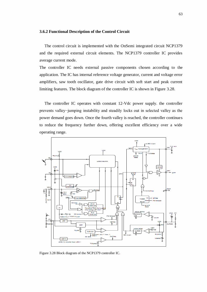
63
3.6.2 Functional Description of the Control Circuit
The control circuit is implemented with the OnSemi integrated circuit NCP1379
and the required external circuit elements. The NCP1379 controller IC provides
average current mode.
The controller IC needs external passive components chosen according to the
application. The IC has internal reference voltage generator, current and voltage error
amplifiers, saw tooth oscillator, gate drive circuit with soft start and peak current
limiting features. The block diagram of the controller IC is shown in Figure 3.28.
The controller IC operates with constant 12-Vdc power supply. the controller
prevents valley−jumping instability and steadily locks out in selected valley as the
power demand goes down. Once the fourth valley is reached, the controller continues
to reduce the frequency further down, offering excellent efficiency over a wide
operating range.
Figure 3.28 Block diagram of the NCP1379 controller IC.

64
Due to a fault timer combined to an OPP circuitry, the controller is able to
efficiently limit the output power at high−line. NCP1379 optimizes the efficiency by
switching in the valley of the MOSFET drain−source voltage. Due to a proprietary
circuitry, the controller locks−out in a selected valley and remains locked until the
output loading significantly changes. This behavior is obtained by monitoring the
feedback voltage.
When the load becomes lighter, the feedback setpoint changes and the controller
jumps into the next valley. It can go down to the 4th valley if necessary. Beyond this
point, the controller reduces its switching frequency by freezing the peak current
setpoint.
Figure 3.29 Output Load is Decreased from 2.4 A to 0.5 A at 120 Vdc Input Voltage
3.7 Design of the Average Current Controlled Circuit
In this section, design procedure for implementing average current mode
controlled PFC with NCP1379 IC is presented. First, the design specification for the
circuit is defined as given in Table 3.2.

65
Table 3.2 Design parameters of 250W average current PFC
Output Power, P0 250 W
Input Voltage, Vin 90-270V
Input Voltage Frequency 50Hz
Switching Frequency 100 kHz
Output Voltage, V0 385V
Input current THD 3%
Efficiency 90%
Hold-up time 50ms
Inductor Current Ripple 20%
The design process is realized by using following procedure.
1) Power stage considerations
2) Selection of the switching frequency fs
3) Selection of the boost inductor L
4) Selection of the output capacitor C0
5) Selection of the power switch elements, MOSFET and PFC diode
Average current mode controlled PFC with NCP1379 controller IC is
implemented with the selected external elements. The schematic diagram of the
hardware is shown in Figure 3.30.
Figure 3.30 Schematic diagram of Primary side the 250-W, average current controlled PFC.

66
1) Power Stage Considerations: A 250-W single-phase power factor correction
circuit is implemented and tested in the laboratory conditions. The average current
mode control has no limit for the power level of the PFC system. Traditionally, the
SMPS has lower power levels that are used in commercial equipments. So, 250-W
PFC is a good example to show the basics of the average current mode controlled
PFC circuit. The PFC circuit is designed to operate anywhere in the world (universal
input line).
The first issue to design the power stage is defining the output voltage level. The
output voltage should be greater than the peak of the maximum input voltage. In this
example, output voltage reference is selected as 385 Vdc. The main elements of the
circuit are boost inductor, power switch, boost diode and output capacitor. The boost
inductor is designed for the inductor ripple current at the worst case operation of the
circuit. The selection of the power switch is done by considering the rms value of the
switch current. The boost diode should have fast reverse recovery characteristics for
CCM operation. Both power switch and diode should be rated at about 20 % above
of the output voltage. The output capacitor should be selected by considering the
output voltage ripple and hold-up time.
2) Selection of the switching frequency fs: Switching frequency should be high
enough to reduce power component size but low enough to reduce the power losses.
So selection of the switching frequency is defined by the trade-off between size and
switching losses. The controller provides wide range of switching frequency (20
kHz-250 kHz). In this example, 21,439 kHz switching frequency is selected for
better utilization and smaller circuit elements.
5 (3.25)

67
Figure 3.31 Switching frequency measurement
3) Selection of the boost inductor L: The boost inductor determines the high
frequency ripple for the inductor current. Inductor is designed to handle maximum
peak current and defined current ripple. First, the maximum peak current that occurs
in operating at minimum input voltage has to be defined. The maximum input peak
current Iin,peak(max) is ;
The peak to peak ripple current is defined as 20% of the maximum input peak
current. So the high frequency ripple current is:
∆l=0.2 x =0, 9A (3.26)
The value of the inductor is selected at the maximum input current and low input
voltage with corresponding duty ratio, D.
D=
3 5 (3.27)
where D is the duty cycle, fs is the switching frequency and _I is the inductor current
ripple. A 900 uH, ferrite core, high frequency inductor is used with 6-A current
handling capacity.
L=
1 kH A (3.28)

68
4) Selection of the Output Capacitor C0: The capacitance and the rated voltage
value should be designed according to predefined output voltage, output voltage
ripple and hold-up time for the output voltage. Total current through the output
capacitor is the rms value of the high frequency ripple current and second harmonic
of the line current. The capacitor with voltage and current ratings grater than the
normal operating point values with smaller ESR is selected. Hold-up time is the other
selection criterion for the selection of the capacitance. Hold-up time is the length of
the time where the output voltage remains within the specified range after input
voltage is turned off. In this example hold-up time is selected as 20 ms. Calculating
the capacitance is done according to the equation (3.29).
C0=
(3.29)
where ∆I is the hold-up time. 220 F, 450-V electrolytic capacitor with lower ESR
is chosen for 385-V output voltage and 250-W output power.
5) Selection of the power switches elements, MOSFET and PFC diode: The
selection of the switch elements, power switch and boost diode, depends on
thevoltage and current ratings, and switching losses. The power switch and diode
shouldhave sufficient operation ratings. Power losses should be considered while
selectingpower switch. Total power loss is the sum of the switching loss and
conduction loss.
Choosing a switch with minimum gate charge and switch capacitance reduces the
turn-on and turn-off losses. A small on-resistance will reduce the conduction losses.
A power MOSFET with current rating higher than the maximum peak current of the
inductor and voltage rating greater than the output voltage is chosen as power switch.

69
3.8 Experimental Results
The Boost converter has been designed to support general types of TV
applications with up to 3 output voltages which can be selected by transformer
design with adapted turn’s ratio of each secondary winding. The first application that
has been developed supports the most common application working with 5 V and 12
V, with 50 W continuous power, up to 70 W peak with up to 4 A on each of the 2
outputs.The third output could be used for a 24 V most likely dedicated to Audio
amplifiers with lower current capability limited to 1 A or 2 A peak.
Connected to the auxiliary winding through R205, the ZCD / pin 1 detects the
core reset event such that the controller will always drive the system with full
demagnetization. The value of the small capacitor C210 (with both R205 and R211)
will set the delay to switch by the minimum voltage and reduce as much as possible
switching looses and EMI. This will be true even by the fourth valley when the
output power is low.
Also, injecting a negative voltage smaller than 0.3 V on this pin during the
conduction of the power MOS will perform over power protection defined by R206.
The diode D203 allows both ZCD and OPP individual adjustment.
Figure 3.31 Experimental measurement of ZCD pin of IC NCP1379.

70
The secondary feedback opto coupler collector connected to the FB / pin 2 will
allow regulation via primary current regulation, lower voltage on this pin will
immediately reduce the output power.
Figure 3.32 Experimental measurement of FB pin of IC NCP1379.
The CS / pin 3 monitors the primary peak current going through the Power MOS
Q203 and the primary of the transformer. If the first level of 0.8 V limits the current
cycle by cycle and start the internal timer, the second level of 1.2 V (150%) will
switch OFF immediately and latch the IC as this is the result of strong secondary
diode short circuit. The GND / pin 4 is connected to the primary ground.
The DRV / pin 5 is the driver’s output which directly drives the gate of external
Power MOS Q203. Although the IC is designed to directly drive large Power
MOS, an added external PNP transistor Q204 is used to reduce current loop and
possible EMI related to the high di/dt necessary to switch OFF the Power MOS in
a small amount of time.

71
Figure 3.33 Experimental measurement of DRV pin of IC NCP1379
The Vcc / pin 6 is the supply pin of the IC connected to the general supply Vcc4
through a dedicated filter (R209), after standby switch Q101 with energy coming
from Standby (Vcc1) or Boost (Vcc3) SMPS.
Figure 3.34 Experimental measurement of Vcc pin of IC NCP1379
To avoid direct impact of output power though leakage inductance on the primary
auxiliary voltage Vcc3, a large resistance R207 has been inserted in series to the
rectifier diode to get the closest voltage to the plateau which is the image from output
regulated voltage. This voltage Vcc3 is also used to detect over voltage and acts to
latch the IC through the BO pin protection.

72
The BO / pin 7 observes the HV rail or the voltage coming from PFC OK
(through the divider R203 and R214) to allow starting phase only when PFC-OUT
supply line is correct. It also offers a way to latch the circuit in case of over voltage
event through the diode D206 when the zener diode ZD200 is switch ON (Open
regulation loop protection) and provide 2.5 V to pin 7.
A capacitor connected to the CT / pin 8 acts as the timing capacitor in foldback
mode and adjusts the frequency in VCO mode. As for general Boost application, a
voltage clamp is used to reduce the Max voltage on the Power MOS linked to the
leakage inductance of the transformer. To avoid over temperature, up to 3 power
resistances R200, R251 and R252 can be used.
Figure 3.35 Experimental measurement of CT pin of IC NCP1379
3.9 Summary
The average current mode control PFC circuit is analyzed theoretically and
simulation and experimental results are verified. It is shown that the average current
mode control seems attractive for active power factor correction circuit. However,
there is too much design procedure making the system complex. Also the number of
elements used in the circuit is high. In the following chapters, another active PFC
control method will be analyzed and verified experimentally.

73
CHAPTER FOUR
FREQUENCY CLAMPED CRITICAL CONDUCTION MODE
CONTROL OF PFC
4.1 Introduction
In this chapter, firstly the analysis of single-phase active power factor correction
circuit operated in the critical conduction mode is presented. The critical conduction
mode is also called as boundary conduction mode or transition mode control. The
word ―boundary‖ comes from the operation characteristics of the proposed control
method. In the boundary conduction mode control (BCM), the inductor current
operates at the boundary of continuous conduction mode (CCM) and discontinuous
conduction mode (DCM).After that in section 4.5 gives detail information about
interleaving method which operates frequency clamped critical conduction mode
(FCCrM).( Balogh L. & Redl R. Power-factor correction with interleaved boost
converters in continuous inductor current mode. In: Proc IEEE APEC’93 conf, San
Diego, CA; March 1993. p. 168–74. )
Critical conduction mode operation is the most popular solution for the low power
applications due to the following reasons:
The control topology needs few external components and serves simple
design process
Low cost solution to achieve near unity power factor application
Smaller magnetic element sizes due to the CCM operation
Lower switching losses and stress on the power switch elements in the
application.

74
The power switch turns-on at zero current and the reverse recovery loss of the
boost diode is minimized.
However, the switching frequency of the boundary conduction mode is not
constant and varies over a line cycle. The switching frequency at the zero crossing of
the line is higher in contrary, lower in the peak of the line cycle. So this large
switching frequency variation causes distortions in the input current. Because the
inductor current peak value is twice of the input current peak value, boundary
conduction mode is not suitable for high power applications.
This chapter describes the basics of a PFC boost converter operating at the critical
conduction mode. Operation principle and derivation of circuit parameters are
discussed. Steady-state characteristics, switching frequency derivation, input and
inductor current properties are explained throughout the chapter. Simulation and
experimental results are verified and compared.
4.2 Operation of Critical Conduction Mode
PFC boost converter such as in average current mode control is used to analyze
the basics of the critical conduction mode. A typical critical conduction mode control
is illustrated in Figure 4.1.
Figure 4.1 Block diagram of a BCM boost converter.
The reference current is obtained by the same method as in the average current
mode control scheme. The sensed sinusoidal waveform is multiplied with the output

75
of the voltage error amplifier and required current reference is built. The switch
current is sensed. The power switch is turned on when the inductor current drops to
zero. The power switch is turned off when the inductor current reaches the reference
current.
Thus inductor current has a triangular waveshape with a sinusoidal envelope. An
input filter capacitor is used to average the triangular waveshape thus providing a
sinusoidal input current. The resulting waveforms of inductor current IL, averaged
input current IAC and reference current IREF are shown for a half line cycle in Figure
4.2.
Figure 4.2 Current waveforms during half of an AC line cycle
In critical conduction mode, boost converter operates in two modes. The inductor
current builds up linearly with the slope (Vin/L) during on time. Theoretically, the
on-time duration of the power switch is constant. However, due to finite switching
frequency, the switch on time varies throughout the entire cycle. Second mode
begins with the turning-off of the power switch. The inductor current decreases
linearly with the slope (V0 - Vin / L). This switching sequence repeats at every zero
crossing of the inductor current. So the inductor current is zero when the switch is
turned on. This provides a zero current turn-on, hence minimizes the switching
losses. These conduction modes are illustrated in Figure 4.3.

76
Figure 4.3 Switching sequences of PFC Stage
The critical conduction mode control eliminates the inner current controller. A
simple on-off control with a zero current detector block is enough to implement a
boundary conduction mode control. In addition only switch current is sensed.
As a result, the inductor peak current is twice of the line peak current at the
boundary conduction mode. This control topology requires smaller boost inductor
but requires input filtering capacitor to smooth the current and minimize the EMI.
Design procedure is simple and low cost. It is suitable for low power applications
due to higher peak currents and variable switching frequency.( Elmore MS.‖Input
current ripple cancellation in synchronized, paralel connected critically continuous
boost converters‖. In: Proc IEEE APEC’96 conf, San Jose, CA; March 1996. p. 152
8. )
4.3 Analysis of Switching Characteristics Critical Conduction Mode
In this section, steady-state characteristics, switching-on and -off time, duty cycle,
switching frequency and their dependency on ac input voltage and power level are
discussed.
The BCM boost converter operates as a power factor pre-regulator so the input
voltage and input current of the system have sinusoidal waveform without any

77
displacement. Thus the sinusoidal equations for the input voltage Vin(t) and input
current Iin(t) can be expressed as follows:
(4.1)
And
(4.2)
The operation of the BCM control is explained in section 4.2. Actual and averaged
inductor currents with corresponding gate signals are illustrated in Figure 4.4.
Figure 4.4 Inductor Current and Corresponding Gate Signals
The input current Iin is equal to the averaged inductor current IL that is half of the
peak value of the inductor current IL,peak.
(4.3)
where Ts is the switching period. So peak inductor current can be written by using
equation (4.4) as:
(4.4)

78
The basic input power definition can be used for the derivation of the peak inductor
current. The averaged input power is equal to the product of the rms values of the
input voltage and current. Averaged input power can be expressed as:
(4.5)
Peak inductor current is a function of averaged power and rms value of input voltage
x (4.6)
The BCM converter operates with variable switching frequency as illustrated in
Figure 4.3. As already stated, the inductor current consists of two phases. During the
on time of the power switch, the inductor voltage is equal to the input voltage and
inductor current increases with a Vin/L slope. The inductor current in the on time can
be expressed as:
(4.7)
At the end of the on-time duration, the inductor current IL is equal to the peak
inductor current IL,peak. Thus
(4.8)
The on time is then expressed by using equation (4.1) and (4.6) as:
(4.9)
It is clear from equation (4.9) that, the on time ton is constant during line cycle.
The on-time duration depends on power level, inductance and input rms voltage. The

79
off time duration can be explained by using the second phase of the inductor current.
During this second phase, inductor current flows through the output diode and feeds
the output capacitor and load.
The inductor voltage becomes negative and inductor current decreases with a
linear (V0 - Vin )/L slope. The inductor current is equal to the peak value at the
beginning of the off-time duration and drops to zero at the end of this second phase.
The variation in the inductor current in the second phase can be
written as:
(4.10)
This second phase ends when the inductor current reaches zero, and the off time is
given by the following equation:
(4.11)
Off-time duration is not constant and varies during each half cycle. Total switching
period is the sum of ton and toff. Thus
Ts= ton + toff (4.12)
The equation for the switching period TS can be expressed by using equation (4.1)
and (4.6) as:
(4.13)
Thus the switching frequency fs is the inverse of the switching period TS.

80
Consequently,
x
(4.14)
This equation shows that, the switching frequency consists of a constant component
that has a value dependent on the operating point and a variable component that
makes the switching frequency vary within AC line cycle. The following figure
illustrates the variations of the switching frequency within a half AC line cycle.
Figure 4.5 Switching frequency over the AC line cycle
The switching frequency is high near the zero crossings of the line cycle where
the inductor current has lower amplitude. Besides, the switching frequency is
approximately divided by five at the top of the sinusoid, where the inductor current
has higher amplitude. In actual implementation, the rectified input voltage is filtered
with a high frequency AC capacitor to provide a clean reference waveform. The
output voltage error amplifier determines the amplitude of the current reference.
The turn-on time is controlled by the comparison of the reference and the actual
inductor current. The power switch is turned on when the actual inductor current
drops to zero and turned off when actual inductor current reaches the reference. In
the next section, computer simulation analysis of a CCM converter will be verified.

81
4.4 Simulation of Critical Conduction Mode PFC
Single-phase critical conduction mode controlled PFC circuit is simulated by
SIMPLORER simulation tool and simulation results are verified. The simulated
circuit and control blocks are shown in Figure 4.6.
Figure 4.6 Block diagram of simulation circuit
Computer simulation of critical conduction mode control is used for the analysis
of circuit parameters and waveforms at different operating points. The input current,
inductor current, switching signals and output voltage waveforms are illustrated and
analyzed. The current waveform behavior for different input voltages and the output
voltage differences at step load conditions are verified. The circuit is simulated with
the following simulation parameters given in Table 4.1.

82
Table 4.1 Simulation parameters of critical conduction mode PFC
Output Power, P0 150 W
Input Voltage, Vin 90-265V
Input Voltage Frequency 50Hz
Switching Frequency Variable
Output Voltage, V0 400V
Boost Inductor, L 0.8mH
Output Capacitor, C0 330uF
Integration Formula Euler
Minimum Step Time 0.1u
The output voltage controller is a low bandwidth voltage error amplifier that is
built with s-transfer function block in the simulation tool. The crossover frequency of
the voltage controller is chosen as 20 Hz. A 400-V reference voltage is used in the
comparator at the input of the voltage error amplifier. There is no inner current
controller in the critical conduction mode control. Simply an on-off control is applied
in the simulation tool. Inductor current is compared with the switch current. (Lee
PW., Lee YS., Cheng DKW., & Liu XC.‖ Steady-state analysis of an interleaved
boost converter with coupled inductors‖. IEEE Trans Ind Electron 2000;47(4):787–
95. )
Figure 4.7 S-Transfer function for the voltage and current controller used in simulation

83
The control algorithm for this type of control is realized by using equation block
tool in the simulation. The voltage controller s-transfer function block (GS1) and
current control equation block (EQUBL1) are shown in Figure 4.7.
The circuit is simulated for 220 Vac input voltage and 150 W output power. The
input voltage, and generated inductor current reference and the actual inductor
current waveforms are illustrated in Figure 4.8. The corresponding input current is
shown in Figure 4.9.
Figure 4.8 Line voltage, reference inductor current and actual inductor currentsimulation waveforms
for 220 V input voltage at 150 W PFC (current scale: 40x).
Figure 4.9 Line voltage and input current simulation waveforms for 220 V input voltage at 150 W
PFC system (current scale: 40x).

84
The output voltage reference is set to 400 Vdc level. The output voltage waveform at
steady state with the input current is illustrated in Figure 4.10.
Figure 4.10 Output voltage and input current simulation waveforms for 220 V input voltage at 150 W
PFC system (current scale: 100x).
The transient response for the output voltage at the start-up and step load response
are verified in the simulation. The load is increased at steady state and corresponding
output voltage waveform is illustrated in Figure 4.11.
Figure 4.11 Transient response for output voltage simulation waveforms for 220 V input voltage at
start-up and half-load to full-load step.

85
4.5 Operation Interleaved PFC System
In high power applications, interleaved operation (the paralel connection of
switching converters) of two or more boost converters has been proposed to increase
the output power and to reduce the output ripple. This technique consists of a phase
shifting of the control signals of several cells in parallel operating at the same
switching frequency.
As a result, the input and output current waveforms exhibit lower ripple amplitude
and smaller harmonics content than in synchronous operation modes. The resulting
cancellation of low-frequency harmonics allows the reduction of size and losses of
the filtering stages. Moreover, a converter employing the interleaving strategy can
feature a great power density without the penalty of reduced power-conversion
efficiency.
However, current sharing among the parallel paths in continuous inductor current
and at average current control is a major design problem because of the mismatch in
duty cycle.( Braga HAC.,& Barbi I. A ―3-kW unity-power-factor rectifier based on a
two-cell boost converter using a new parallel-connection technique‖. IEEE Trans
Power Electron 1999;14(1):209–17.)
Higher power density and faster transient response can be achieved by increasing
switching frequency. In Figure 4.12 a general structure for an N–phase interleaved
boost converter is given. Mathematically there is no limit for the number of
interleaved power branches. But, in practice as the phase number increases, the
system complexity increases and maintenance becomes difficult.

86
Figure 4.12 N–Phase interleaved boost converter.
Higher switching frequency causes increase in switching losses and a serious
electromagnetic interference (EMI) problem in hard switched PWM converters. The
switching losses of the boost switches make a significant amount of power
dissipation. Therefore, the switching losses of the converter should be minimized to
increase the efficiency and power density by using soft switching techniques. These
techniques are implemented by passive or active snubber circuits.
Various kinds of soft switching techniques have been proposed in the literature to
minimize switching losses of the boost converters. Converters operating at soft
switching with passive snubbers are attractive, since there is no need for extra active
switches and also the control scheme is simpler. The main problem with these kinds
of converters is that the voltage stresses on the power switches are too high and the
converter is bulky. The study presented in is an example for this type application in
which the active power switches of the converter are turned on at zero voltage
switching by which the switching losses are reduced. The auxiliary inductor used in
this circuit is very big (nearly half of the main inductors) and this results in a bulky
circuit.

87
Figure 4.13 The scheme of controller power stage of the proposed topology
Active auxiliary snubbers are also developed to reduce switching losses of boost
and interleaved boost converters without having the disadvantages of passive
auxiliary circuits. These active snubbers have additional gate circuits for the
auxiliary switches to generate their gate pulses and to synchronize them with the
main switch.
4.6 Interleaved PFC Technique Analysis of Switching Characteristics
By using the segmentation, phase shifting and merging principles, the output
power level is possible to be increased without sacrificing the converter efficiency, as
well as high power density can be obtained due to small inductance values with
lower operating frequency can be utilized with no penalty in term of input and output
current stresses. Moreover, minimum external heatsink and a simple controller in
CCM operation can be achieved. Fig. 4 shows a two-cell structure where capacitor
C1 can be used together.
Consequently, smaller current stress of this capacitor normally is reduced, as can
be seen in Fig. 4(c). It is clear that the interleaving technique also allows significant
reduction for inductor L1 without introducing electromagnetic interference (EMI)
problem, as shown in Fig. 4(b).

88
Fig 4.14 Proposed interleaved PFC boost converter system and the operation waveforms
In principle, the switching cycle of the proposed interleaved boost PFC converter
system can be divided into six stages:
Stage I:
During interval T0 -- T1, in steady state operation, switch S1 is on, switch S2 and
diode D1 are off, and diode D2 is on. Diode D2 releases the energy stored in L3 to
the load, and inductor current IL2 increases linearly. At the same time, the current
flows directly from input to the load through inductor L1, diode rectifier and
capacitor C1. There is a very small voltage drop across inductor L1 due to zeroripple
phenomenon. The voltage stress across C1 is VC1 = Vo - VREC
Fig 4.15 Interval T0—T1

89
Stage II:
During interval T1 -- T2, due to the CCM operation, there is no energy stored in
L3. Therefore, diode D2 is off. In this condition, the energy stored in C1 is
discharged to the load through L2 and S1.
Fig 4.16 Interval T1—T2
Stage III:
During interval T2 -- T3, switch S1 is off and diode D1 is forward biased. Thus,
the energy stored in inductor L2 is transferred to the load through diode D1. At the
same time, the current flows directly from input to the load through inductor L1 and
capacitor C1. Hence, C1 is charged, and IL1 = Io.
Fig 4.17 Interval T2—T3

90
Stage IV:
During interval T3 -- T4, due to the phase shifting principle, switch S2 is on,
switch S1 and diode D2 are off, and diode D1 is on. In this condition, the current
flows from input to L1, L3 and S2. Also, the energy stored in L2 is delivered to the
load through diode D1. Therefore, inductor current IL2 decreases linearly and
inductor current IL3 increases linearly, but inductor current IL1 is always continuous
and operates in zero-ripple fashion. At the same time, the current flows directly from
input to the load through inductor L1 and capacitor C1. Consequently, capacitor C1
is charged.
Fig 4.18 Interval T3—T4
Stage V:
During interval T4 -- T5, due to the DCM operation, the inductor current IL2
reaches zero at T = T4. It causes diode D1 off. Switch S2 is on until T = T5, At the
same time, the energy stored in capacitor C1 is discharged to the load through
inductor L3 and switch S2.
Fig 4.19 Interval T4—T5

91
Stage VI:
During interval T5 -- T6, switch S2 is off, switch S1 and diode D1 are off, and
diode D2 is on. Thus, the energy stored in inductor L3 is transferred to the load
through diode D2. In this condition, the current also flows from input to the load
through inductor L1 and capacitor C1. This causes capacitor C1 is charged again and
inductor current IL1 = Io. In this case, the current flows from the ac line through
inductor L1.
Fig 4.20 Interval T5—T6
It is interesting that the characteristics of` the proposed interleaved boost PFC
converter system not only ripple-free input current with separate inductors can be
obtained, but also the energy transfer mechanism occurs during the main switch both
on and off.
4.7 Simulation of Interleaved PFC
Fig 4.21 Circuit Schematic

92
Fig 4.22 Simulation results of iL1–iL2–ig (for V=230V)
Figure 4.22 and Figure 4.23 are full load at low line and highline voltage.As
expected, the input current has the shape of a CCM current. At low line and high
line, the phase shift is well controlled and is 180°. Each branch operates in CRM at
low line and in DCM fixed frequency at high line which is called FCCrM structure.
Fig 4.23 Simulation results of iL1–iL2–ig (for V=90V)

93
Fig 4.23 Simulation results of Vd & İd (for V=90V)
According to these results, the auxiliary switch is turned on and off under soft
switching conditions.Figs 4.23 and 4.24 show the simulation and experimental
results of the voltage of resonant capacitor used in the auxiliary circuit.The switching
operations of the output and auxiliary circuit diodes are also observed via simulation
and experimental studies. It is observed that the output diodes and auxiliary circuit
diodes turn on and turn off under soft switching and there is no voltage stress on the
diodes.. An experimental circuit for conventional hard switched interleaved boost
converter is also built up to compare with the pro- posed soft switched topology.
Fig 4.24 Simulation results of Vd & İd (for V=230V)

94
4.8 Hardware Implementation of Boundary Conduction Mode PFC
In this section, the implementation of the average current mode control boost
converter with PFC controller IC is explained. The analog PFC controller IC,
NCP1631, is chosen to implement frrequency clamped critical conduction mode PFC
application. General specifications of the power circuit and control circuit elements
of an critical conduction mode power factor correctionsystem is derived. The single-
phase PFC is shaped from a single-phase diode rectifier and a cascaded DC/DC boost
converter. The types of the components in the power circuit with their general
specifications are summarized briefly in subsection 4.4.1. The general parameters
and the block diagram of the controller are given in subsection 4.4.2.
4.8.1 Functional Description of the Power Circuit
Single-phase bridge rectifier with a cascaded boost converter is built and critical
conduction mode control is applied. The load is chosen as a resistive load. Input is
supplied by an isolated variable AC power supply. A high-frequency filtering
capacitor is installed after the bridge rectifier to smooth the output of the rectifier.
The boost inductor, boost diode, power switch and output capacitor assume the
power factor pre-regulator role. The ratings for the switching elements are chosen by
considering maximum peak current levels. A fast acting glass fuse and a bypass
diode are placed in the circuit to prevent the components in the case over current.
Also an NTC is placed in the input of the circuit to limit the start-up current due
to initial charge of the output capacitor. At steady state, the resistance of this NTC is
very small, thus provides minimum power loss in the NTC. A sensing resistor with
smaller resistance is placed at the source of the power MOSFET to sense the switch
current. Auxiliary windings in the boost inductor are used for the zero current
detection of the inductor current. Also these windings are used to supply controller
IC.

95
4.8.2 Functional Description of the Control Circuit
Average current control mode is implemented by the ON Semiconductor
integrated circuit NCP 1379 with selected passive elements. The NCP1631
controller is the one of the most popularfrequency clamped critical conduction mode
IC for PFC due to easy design requirements. The controller has internal voltage
reference generator, trans-conductance type voltage error amplifier, multiplier, zero
current detector, over voltage comparator etc. The block diagram of the controller IC
is shown in Figure 4.25
Fig 4.25 Block Diagram of NCP 1631 Interleaved PFC IC
The NCP1631 is designed for use in a pre-regulator in electronic ballasts and off-
line power supplies applications. The controller consists of all required control
blocks including protection blocks. Also gate drive circuit is adequate to drive any
power switch element such as MOSFET or IGBT. The controller has internal output
voltage error amplifier. The inverting and output pins of this error amplifier are
accessible. The non-inverting input is connected internally to the voltage reference.
The output voltage divider feedback should be scaled to this reference level. The
error amplifier is a transconductance type, meaning that is has high output impedance
with controlled voltage-to-current gain. The gain of transconductance is around 100
mhos.

96
The transconductance type amplifier provides better performance; also the inverting
input of the amplifier can be used for different purposes such as over voltage
comparator.
The compensation passive elements are placed between the output of the
amplifier and ground. An overvoltage comparator is used to protect the circuit in
case of over voltage at the output capacitor. The overvoltage limit is set to 1.08 of the
reference output voltage. When this limit is exceeded, the gate is turned off until
safety limits are reached again.
The multiplier is the core of the system. The inputs for the multiplier are the
output of the voltage error amplifier and current waveform reference. The output of
the multiplier is the reference inductor current. The actual inductor current is forced
to flow between this reference and zero.
An internal zero current detector is used to turn on the power switch when the
inductor current drops to zero. This inductor current information is taken from the
auxiliary windings of the boost inductor. The zero current detector initiates the next
On time by setting the RS Latch at the instant the inductor current reaches zero. An
internal watch dog timer is used to start or restart the converter if the drive output has
been off more than 600 usec after the inductor current reaches zero. The control IC is
supplied with an auxiliary supply circuit.
There is no need of external power supply. An undervoltage lockout comparator
has been incorporated to guarantee that the IC is fully functional before enabling the
output stage. In the next section, design of the 150W PFC circuit with NCP1631 is
explained.( Bodur H. & Bakan AF. ―A new ZVT–ZCT–PWM DC–DC converter‖.
IEEE Trans Power Electron 2004;19(3):676–84.)

97
4.9 Design of the Frequency Clamped Critical Conduction Mode PFC
Converter
In this section, design procedure for implementing frequency cllamped critical
conduction mode controlled PFC with NCP1631 IC is presented. The circuit is
implemented for low power applications. First, the design specifications for the
circuit are defined as given in Table 4.2.
Table 4.2 Design parameters of current conduction PFC
Output Power, P0 150 W
Input Voltage, Vin 85-270V
Input Voltage
Frequency
50Hz
Switching Frequency Variable
Output Voltage, V0 400V
Input current THD 3%
Efficiency 90%
Hold-up time 50ms
The design process is realized using the following design procedure.
1) Power stage considerations
2) Switching frequency fs considerations
3) Selection of the boost inductor L
4) Selection of the output capacitor C0
Frequency clamped critical conduction mode controlled PFC with NCP 1631
controller IC is implemented with the selected external elements. The schematic
diagram of the hardware is shown in Figure 4.26

98
Fig 4.26 Typical Application Schematic Diagram of NCP 1631 Interleaved PFC IC
1) Power Stage Considerations:
A 150-W single-phase power factor correction circuit is implemented and tested
in the laboratory conditions. The critical conduction mode control is suitable for the
low power applications. The circuit is designed to operate with universal input
voltage range. A resistive load or a DC/DC converter can be used as load of the
circuit. A resistive load is used to carry out experiments in the laboratory.
The output voltage reference is set to 400 Vdc with 430 Vdc over voltage
protection. The main elements of the circuit are boost inductor, power switch, boost
diode and output capacitor. The boost inductor is designed with auxiliary windings to
be used in the zero current detector. The selection of the power switch is done by
considering the rms value of the switch current. The boost diode should have fast
reverse recovery characteristics for FCrCM operation. Both power switch and diode
should be rated about 20% above of the output voltage. The output capacitor should
be selected by considering the output voltage ripple and hold-up time.

99
2) Switching frequency fs considerations:
The switching frequency is variable in the critical conduction mode control. The
variation of the switching frequency during a line cycle is explained in section 4.3.
The switching frequency characteristics for different input level are analyzed by
using equation (4.14). The deviations in the switching frequency for the 220 Vac
input voltage is shown in Figure 4.27. Figure 4.28shows the switching frequency
variations for 120 Vac input voltage.
Figure 4.27 Switching frequency for 220VAC line voltage for critical current mode PFC.

100
Figure 4.28 Switching frequency for 120VAC line voltage for critical current mode PFC.
3) Selection of the boost inductor L:
The inductance is designed for minimum switching period. Assuming that the
minimum switching period is equal to 40 usec for the universal line (85-270), the
inductance value can be calculated as:
=
= 600 uH (4.15)
The inductor is built from ferrite core material. The primary of the inductor is
measured as 700 uH. 80 turns are placed in the primary of the inductor. Auxiliary
windings are placed in the secondary for zero current detection and power supply for
the controller IC. 5 turns are placed in the secondary.

101
4) Selection of the Output Capacitor :
The output capacitor defines the output voltage ripple and hold-up time for the
PFC. The capacitance and the rated voltage value should be designed regarding the
predefined output voltage, output voltage ripple and hold-up time for the output
voltage. The capacitor with voltage and current rating greater than the normal
operating point values with smaller ESR is selected. In this example a 330 uF
electrolytic capacitor is used and corresponding output voltage ripple is shown in
Figure 4.29
Figure 4.29 Output voltage ripple.
4.10 Experimental Results
The NCP1631 integrates a dual MOSFET driver for interleaved, 2−phase PFC
applications. It drives the two branches in so−called Frequency Clamped Critical
conduction Mode (FCCrM) where each phase operates in Critical conduction Mode
(CrM) in the most stressful conditions and in Discontinuous Conduction Mode
(DCM) otherwise, acting as a CrM controller with a frequency clamp (given by the
oscillator). According to theconditions, the PFC stage actually jumps from DCM to
CrM (and vice versa) with no discontinuity in operation and without degradation of
the current shape.

102
Figure 4.30Interleaved PFC Controller Zero Current Detection Pin. (probe10x)
At Figure 4.30 the zero current detection pin for phase 1and phase2 of the
interleaved PFC stage. Apply the voltage from an auxiliary winding to detect the
core reset of the inductor and the valley of the MOSFET drain source voltage.
Figure 4.31Interleaved PFC Controller Feedback Pin. (probe10x)
At Figure 4.31 receives a portion of the pre−converter output voltage. This
information is used for the regulation and the ―output low‖ detection (VOUTL) that
drastically speed−up the loop response when the output voltage drops below 95.5%
of the wished level.

103
At Figure 4.32 Connect a capacitor to set the clamp frequency of the PFC stage.
If wished, this frequency can be reduced in light load as a function of the resistor
placed between pin 6 and ground (frequency fold−back).
Figure 4.32 Interleaved PFC Controller Oscillator Pin. (probe10x)
If the coil current cycle is longer than the selected switching period, the circuit
delays the next cycle until the core is reset. Hence, the PFC stage can operate in
Critical Conduction Mode in the most stressful conditions.
Figure 4.33 Interleaved PFC Controller Vcontroller Pin. (probe10x)

104
At Figure 4.33 the error amplifier output is available on this pin. The capacitor
connected between this pin and ground adjusts the regulation loop bandwidth that is
typically set below 20 Hz to achieve high Power Factor ratios. Pin5 is grounded
when the circuit is off so that when it starts operation, the power increases slowly
(soft−start).
Figure 4.34 Interleaved PFC Controller Frequency Foldback Pin(probe10x)
Apply a resistor between pin 6 and ground to adjust the oscillator charge current.
Clamped not to exceed 100 uA, this charge current is made proportional to the power
level for a reduced switching frequency at light load and an optimum efficiency over
the load range
Figure 4.35 Interleaved PFC Controller Frequency Foldback Pin(probe10x)

105
At Figure 4.35 Apply a voltage higher than 2.5 V to latch−off the circuit. The
device is reset by unplugging the PFC stage (practically when the circuit detects a
brown−out detection) or by forcing the circuit VCC below VCCRST (4 V typically).
Operation can then resume when the line is applied back.
Figure 4.36 Interleaved PFC Controller Drive Pin(probe10x)
This is the gate drive pin for phase 1 and phase 2 of the interleaved PFC stage.
The high current capability of the totem pole gate drive (+0.5/−0.8 A) makes it
suitable to effectively drive high gate charge power MOSFETs.
Figure 4.37 Interleaved PFC Controller Vcc Pin (probe10x)

106
This pin is the positive supply of the IC. The circuit starts to operate when VCC
exceeds 12 V and turns off when VCC goes below 10 V (typical values). After
start−up, the operating range is 9.5 V up to 20 V
4.11 Summary
In this chapter, the frequency clamped critical conduction mode control of PFC is
discussed. The operation characteristics and dynamic responses are analyzed.
Simulation and experimental implementations are presented. The conceived system
is suitable to test the performance of an average current control of a power factor pre-
regulator.

107
CHAPTER FIVE
CONCLUSIONS AND FUTURE WORK
This thesis is concerned with the power factor correction methods for single-
phase converters. A complete power board that includes active power factor
correction solutions is designed and implemented. The analyzed solutions are
selected in accordance with their benefits, performance and popularity.
The second chapter of the thesis involves the passive power factor correction
methods for a single-phase bridge rectifier. The harmonic filter is analyzed and
designed according to harmonic emission standard IEC 61000-3-2. Theoretical and
experimental results show that, a passive filtering method seems attractive for low
power application due to their low cost and few complexity characteristics. The size
and weight of the filtering elements are disadvantages of the passive filtering
methods.
The third chapter, reviews the active power factor correction methods. A single-
phase diode rectifier with a cascaded boost converter has advantages over the other
topologies. In addition, the control technique for active PFC is analyzed. One of the
control methods is implemented. Of the available control methods average current
control mode is selected due to its performance, popularity and design complexity.
With the experimental result, advantages of implemented control technique is studied
and reviewed. The average current control seems more attractive with its
performance but the design of this type control is more complex.
In the fourth stage, the control techniques for active PFC are analyzed. Two of the
control methods are implemented. These are critical conduction mode and frequency
clamped critical conduction mode. The selected control methods are chosen in
accordance with their performance, popularity and design complexity.

108
The critical conduction mode reduces design complexity however it is suitable for
low power applications due to operating with higher peak current levels.
As a result, the harmonic polluting effects of the single-phase diode rectifier
based power converters are reviewed theoretically and experimentally. The harmonic
limiting standards and the common solutions for power factor correction are
analyzed. The popular passive and active power factor correction schemes are
analyzed and verified with simulation and experimental results.
The final part involves the monolithic chip based control implementation of the
single-phase interleaved PFC converter. This is one of the novel features of the
thesis, as this chip has recently become available on the market and it provides
advantageous features compared to the conventional implementation which involves
the development of such a controller (involving the phase shift between the phases
and the parallel operation of the current loops) by the design engineers. Having
completed the design and system hardware manufacturing, the converter
performance was verified by detailed laboratory experiments.
As a further study, the power board can be improved by using the latest
developments in semiconductor technology. In addition, if warm-up problems at
transformer is solved by changing transformer winding number to the appropriate
values, the power level is increased. Power loss considerations and new techniques to
reduce these losses can be implemented. Finally this thesis includes design and
implementation of such a high efficienct SMPS which is boost DC/DC converter and
it is combined with an interleaved PFC having high performance and small size.

109
REFERENCES
B. Sharifipour., J. S. Huang., P. Liao., L. Huber & M. M. Jovanovic.,(1997). ―Manufacturing
and cost analysis of power-factor-correction circuits,‖ IEEE Applied Power Electronics Conf.
(APEC) Proc., 1997, pp.490-494
Borage, M., Tiwari S., & Kotaiah, S. (2003). "Passive Techniques for Compliance of Single-
phase Rectifiers with IEC 1000-3-2 Norms", Proc. Of International c c conference on
Electromagnetic Interference and Compatibility (INCEMIC) 2003, pp. 18.
Dixon, L. H.(1988). ―High Power Factor Pre regulators for Off-Line PowerSupplies”,
Unitrode Power Supply Design Seminar Manual SEM600, 1988
Dixon, L. H. (1990). ―Optimizing the Design of High Power Factor Switching Preregulator”,
Unitrode Power Supply Design Seminar Manual SEM700, 1990
Dixon, L. (1990). ―Average current mode control of switching power supplies,‖ Unitrode
Switching Regulated Power Supply Design Seminar Manual, SEM- 700,1990.
Dorf, C., Richard, Ed., (2000). ―The Electrical Engineering Handbook‖. EPSMA.(2004),‖
Harmonic Current Emissions Guidelines to the standard EN 61000-3-2 including
amendment” A14, 2004,
www.epsma.org
Fernandez, A., Sebastian, J., Hernando, M.M., Villegas, P.& Garcia, J.(2005). ―Helpful hints
to select a power-factor-correction solution for low- and medium- power single222 phase
power supplies‖ Industrial Electronics, IEEE Transactions on Volume 52, Issue 1, Feb.
2005 Page(s): 46 – 55
IEC61000-3-2, ―Electromagnetic Compatibility (EMC)”—Part 3: Limits—Section 2: Limits
for Harmonic Current Emissions (Equipment Input Current <16A per Phase),
N. Mohan ., T. Udeland., & W. Robbins.(1995). ―Power Electronics: Converters,
Applications and Design”, 2nd ed. New York: Wiley, 1995.

110
Noon, J.P., & Dalal, D.(1997). ―Practical design issues for PFC circuits”, IEEE APEC 1997.
Oscar Gracia., Jose A. Cobos., Roberto Prieto. & JavierUceda.,(2003). ―Single Phase Power
Factor Correction: A Survey‖, IEEE Transactions on Power Electronics, Voi 18,No3,May
2003,pp-749-755.
Prasad, A.R., Ziogas, P. D., & Manias, S. (1990). ―A novel passive wave shaping
method for single-phase diode rectifiers,‖ in IEEE IECON Conf. Proc., 1990, pp. 1041-1050
Redl R., P.Tenti., & V.Wyk.(1997) ―Power electronics polluting effects”, EEE Spectrum,
Volume 34, Issue 5, May 1997
Redl R., 2001). ―Electromagnetic Environmental Impact of Power Electronics Equipment‖,
Proceedings of the IEEE, Vol 89, No:6, June 2001
Redl R., & Balogh L.(1995). ―Power-Factor Correction in Bridge and Voltage- Doublers
Rectifier Circuits with Inductors and Capacitors‖ APEC´95, pp.466 472
Redl,R. & ELFI S.A.(1998). ―An Economical Single-Phase Power-Factor-Corrected
Rectifier: Topology, Operation, Extensions, and Design For Compliance‖APEC´98, pp.454-
460
Ridley, R. B. (1989). "Average Small-Signal Analysis of the Boost Power- Factor- Correction
Circuit", VPEC Seminar Proc., 1989, pp. 108-120.
Scillic. (2004). ―Power Factor Correction Handbook‖.
Singh, B., Chandra, A., Al-Haddad., K. Pandey., & A. Kothari, D.P.(2003).―A review of
single-phase improved power quality AC-DC converters” Industrial Electronics, IEEE
Transactions on Volume 50, Issue 5, Oct. 2003 Page(s): 962- 981

111
Spiazzi, G., Mattavelli, P., & Rossetto, L.(1995)."Methods to Improve Dynamic Response of
Power Factor Preregulators: an Overview", European Power Electronics Conf. (EPE),
Sevilla (Spain), September 1995, Vol.3, pp.754-759.
Supratim Basu., T.M.Undeland., & Fellow.(2004). IEEE. ―PFC Strategies in light of
EN61000-3-2‖. (EPE-PEMC 2004 Conference in Riga, LATVIA, 1- September 2004
TS EN 61000-3-2, ―Elektromanyetik Uyumluluk (EMU)”-Bolum 3-2: Sınır Degerler-
Harmonik Akim Emisyonları _çin Sınır Degerler (Faz Basına Donanım Giris Akımı <16A),
TSE, MART 2003
Williams, J. B.(1989). "Design of Feedback Loop in Unity Power Factor AC to DC
Converter", PESC Conf. Proc., 1989, pp. 959-967.
Yanchao,J., Xiaobing,L., Zhuo,L., Jisheng,J.,& Xinhua,L.,(1996). ―An improved passive input
current waveshaping method for single-phase diode rectifier” IEEE IECON 22nd
International Conference on Volume 2, 5-10 Aug. 1996 Page(s):695 – 699,vol.2
Zhou, C., Jovanovic, M. (1992). "Design Trade-offs in Continuous Current-mode Controlled
Boost Power-Factor Correction Circuits'," HFPC Conf. proc., 1992, pp. 209-220.

112
APPENDIX-A

113

114

115

116

117

118
APPENDIX-B

119

120

121

122

123