TI Designs - 1-kW, Compact, 97.5% Efficiency, Digital PFC for ...
35
12 V (Isolated) 185-V to 265-V AC UCD3138A Digital Controller 390-V DC UCC27517A Gate Drive OPA2376 Amplifier TIDA- 00708 UART PMBUS 3.3 V 12 V 12 V Copyright © 2016, Texas Instruments Incorporated Current Shunt EMI Filter Bridge Rectifier Boost PFC Power Stage Bulk Capacitor ISO7321C 1 TIDUBK8B – May 2016 – Revised October 2016 Submit Documentation Feedback Copyright © 2016, Texas Instruments Incorporated 1-kW, Compact, 97.5% Efficiency, Digital PFC for AC/DC PSUs With eMeter Reference Design TI Designs 1-kW, Compact, 97.5% Efficiency, Digital PFC for AC/DC PSUs With eMeter Reference Design All trademarks are the property of their respective owners. TI Designs The TIDA-00707 is a 1-kW, compact (100-mm×80- mm) power factor correction (PFC) circuit designed for telecom, server, and industrial power supplies. This reference design is a continuous conduction mode (CCM) boost converter, implemented using a UCD3138A Digital Power Supply controller with all protections built-in. Hardware is designed and tested to pass conducted emissions, surge, and EFT (as per EN55014) requirements. Key highlights of this reference design: • Provides a ready platform of front-end PFC to address various power supplies up to 1 kW • Improves overall system performance with lower bus ripple, lower bus capacitance, lower RMS currents, and front-end protections • Meets stringent current THD and power factor norms • Protects for output overcurrent, overvoltage, and undervoltage conditions Design Resources TIDA-00707 Design Folder UCD3138A Product Folder UCC28881 Product Folder UCC27517A Product Folder TLV704 Product Folder OPA2376 Product Folder ISO7321C Product Folder ASK Our E2E Experts . Design Features • Wide Operating Input Range: 195-V to 270-V AC • Designed to Drive Wide Range of Downstream DC/DC Converters and Inverter-Fed Motors up to 1 kW • High Power Factor > 0.99 and < 5% THD From Medium-to-Full Load (50% to 100%); Meets Current THD Regulations as per IEC 61000-3-2 • High Efficiency of > 97% at Full Load Over Entire Operating Voltage Range • No Need for External Cooling up to 55°C Ambient Operation for Loads ≤ 900 W • Communicates Input Power Consumption Information of the Unit Precisely for all Load Conditions • Built-in 12-V/3-W Supply for Housekeeping Power Needs • PMBUS and Isolated UART for Communication • Meets the Requirements of Conducted Emissions Standard – EN55011 Class A, EFT Norm IEC6000- 4-4, and Surge Norm IEC61000-4-5 • PFC Converter Designed With a Small PCB Form Factor (100 mm × 82 mm) Featured Applications • Telecom Rectifiers • Server and Industrial Power Supplies • Online UPS • Power Storage Banks • Motor Drives
-
Upload
khangminh22 -
Category
Documents
-
view
2 -
download
0
Transcript of TI Designs - 1-kW, Compact, 97.5% Efficiency, Digital PFC for ...

12 V (Isolated)
185-V to 265-V AC
UCD3138ADigital
Controller
390-V DC
UCC27517AGate Drive
OPA2376Amplifier TIDA-
00708
UART
PMBUS
3.3 V
12 V12 V
Copyright © 2016, Texas Instruments Incorporated
Current Shunt
EMI Filter Bridge
Rectifier
Boost PFCPower Stage
Bulk Capacitor
ISO7321C
1TIDUBK8B–May 2016–Revised October 2016Submit Documentation Feedback
Copyright © 2016, Texas Instruments Incorporated
1-kW, Compact, 97.5% Efficiency, Digital PFC for AC/DC PSUs With eMeterReference Design
TI Designs1-kW, Compact, 97.5% Efficiency, Digital PFC for AC/DCPSUs With eMeter Reference Design
All trademarks are the property of their respective owners.
TI DesignsThe TIDA-00707 is a 1-kW, compact (100-mm×80-mm) power factor correction (PFC) circuit designed fortelecom, server, and industrial power supplies. Thisreference design is a continuous conduction mode(CCM) boost converter, implemented using aUCD3138A Digital Power Supply controller with allprotections built-in. Hardware is designed and testedto pass conducted emissions, surge, and EFT (as perEN55014) requirements.
Key highlights of this reference design:• Provides a ready platform of front-end PFC to
address various power supplies up to 1 kW• Improves overall system performance with lower
bus ripple, lower bus capacitance, lower RMScurrents, and front-end protections
• Meets stringent current THD and power factornorms
• Protects for output overcurrent, overvoltage, andundervoltage conditions
Design Resources
TIDA-00707 Design FolderUCD3138A Product FolderUCC28881 Product FolderUCC27517A Product FolderTLV704 Product FolderOPA2376 Product FolderISO7321C Product Folder
ASK Our E2E Experts
.
Design Features• Wide Operating Input Range: 195-V to 270-V AC• Designed to Drive Wide Range of Downstream
DC/DC Converters and Inverter-Fed Motors up to1 kW
• High Power Factor > 0.99 and < 5% THD FromMedium-to-Full Load (50% to 100%); MeetsCurrent THD Regulations as per IEC 61000-3-2
• High Efficiency of > 97% at Full Load Over EntireOperating Voltage Range
• No Need for External Cooling up to 55°C AmbientOperation for Loads ≤ 900 W
• Communicates Input Power ConsumptionInformation of the Unit Precisely for all LoadConditions
• Built-in 12-V/3-W Supply for Housekeeping PowerNeeds
• PMBUS and Isolated UART for Communication• Meets the Requirements of Conducted Emissions
Standard – EN55011 Class A, EFT Norm IEC6000-4-4, and Surge Norm IEC61000-4-5
• PFC Converter Designed With a Small PCB FormFactor (100 mm × 82 mm)
Featured Applications• Telecom Rectifiers• Server and Industrial Power Supplies• Online UPS• Power Storage Banks• Motor Drives

Key System Specifications www.ti.com
2 TIDUBK8B–May 2016–Revised October 2016Submit Documentation Feedback
Copyright © 2016, Texas Instruments Incorporated
1-kW, Compact, 97.5% Efficiency, Digital PFC for AC/DC PSUs With eMeterReference Design
An IMPORTANT NOTICE at the end of this TI reference design addresses authorized use, intellectual property matters and otherimportant disclaimers and information.
1 Key System Specifications
Table 1. Key System Specifications
PARAMETER TEST CONDITIONS MIN NOM MAX UNITINPUT CONDITIONSInput voltage (VINAC) 195 230 270 VACFrequency (fLINE) 47 50 63 HzNo load power (PNL) VINAC = 230 V, IOUT = 0 A — 2.2 — WOUTPUT CONDITIONSOutput voltage — 390 — VOutput current — — 2.56 ALine regulation — — 0.5 %Load regulation — — 0.5 %Output voltage ripple Peak to peak — 20 — VOutput power (PO) — 1000 1000 WSYSTEM CHARACTERISTICSEfficiency (η) VIN = VNOM and full load — 97 — %
Protections
Output overcurrent — — — —Output overvoltage — — — —Output undervoltage — — — —Open-loop detection — — — —
Operating ambient Open frame –10 25 55 °C
Standards and norms
Power line harmonics As per EN55011 / EN55022 Class AConducted emissions As per IEC 61000-3-2 Class AEFT As per IEC-61000-4-4Surge As per IEC-61000-4-5
Board form factor(FR4 material, 2 layers) Length × Breadth × Height 100 × 80 × 40 mm

www.ti.com System Description
3TIDUBK8B–May 2016–Revised October 2016Submit Documentation Feedback
Copyright © 2016, Texas Instruments Incorporated
1-kW, Compact, 97.5% Efficiency, Digital PFC for AC/DC PSUs With eMeterReference Design
2 System DescriptionThe power supplies for telecom, server, and industrial systems convert AC line power to isolated constantDC voltage of –48 V in telecom systems, 12 V in server systems, and 24 V in industrial systems. Thesehigh-power systems typically range from 1 to 5 kW. These power supplies need a front-end power factorcorrection circuit to shape the input current of the power supply and to meet the power factor and currentTHD norms such as IEC61000-2-3.
A power factor correction (PFC) circuit shapes the input current of the power supply to be in phase withthe mains voltage and aids to maximize the real power drawn from the mains. In addition, a PFC front-endoffers several benefits:• Reduces RMS input current
A power circuit with a 230-V/5-A rating is limited to about 575 W of available power with a PF of 0.5.Increasing the PF to 0.99 will double the deliverable power to 1138 W, allowing higher-power loads tobe operated.
• Facilitates power supply holdupThe active PFC circuit maintains a fixed intermediate DC bus voltage that is independent of the inputvoltage, so the energy stored in the system does not decrease as the input voltage decreases. Thisallows the use of smaller, less expensive bulk capacitors.
• Improves efficiency of downstream convertersThe PFC reduces the dynamic voltage range applied to the downstream inverters and converters,reducing voltage ratings of rectifiers results in lower forward drops, and increasing operating duty cycleresults in lower current in switches.
• Increases the efficiency of the power distribution systemA lower RMS current reduces distribution wiring losses.
• Reduces the VA rating of standby power generators and stresses on neutral conductorsReducing harmonics eliminates the risk of triplen harmonics (the third and multiples thereof) that canadd up to dangerous levels in the neutral conductor of Y-connected 3-phase systems.
This reference design is a boost power factor converter implemented by using the UCD3138A as the PFCcontroller for telecom, sever, and industrial systems that demand a PFC up to 1 kW. The design providesa ready platform of active front-end to operate downstream DC/DC converters or inverters operating onHi-line AC voltage range from 195-V to 270-V AC.
Telecom, server, and industrial power supplies require high efficiency over their entire operating voltagerange and wide load variations from 50% to 100% load. This design demonstrates a high-performancepower factor stage in a small form factor (165 mm × 95 mm), operating from 195-V to 270-V AC, anddelivers up to 1 kW of continuous power output at an efficiency of greater than 97%. The design alsoprovides precise information on power consumption of the end equipment from the AC input line, whichcan be used for energy calculations and control the load for power optimization on need basis. The EMIfilter at the front end of the circuit is designed to meet EN55011 class-A conducted emission levels.
The design uses a 5-W housekeeping power supply board (TIDA-00708), which is designed to meet theauxiliary needs of a general power supply. It supports an input voltage range from 100-V to 450-V DC andprovides a 3.5-V DC (1.5-W) and 12-V DC (2.5-W) non-isolated outputs. In addition, a 12-V DC (1-W)isolated output is also provided to support downstream auxiliary power needs. The features of the powersupply board include easily pluggable, compact size (LXBXH), high efficiency, low no-load powerconsumption, and low cost. Find more details of this power supply in the design guide of the powersupply, TIDA-00708 (TIDUBK7).
This TI Design meets the key challenges of telecom, server, and industrial power supplies to provide safeand reliable power with all protections built in while delivering high performance with low powerconsumption and a low bill-of-material (BOM) cost.

12 V (Isolated)
185-V to 265-V AC
UCD3138ADigital Controller
Current Shunt
EMI Filter Bridge
Rectifier
390-V DC
UCC27517AGate Drive
OPA2376Amplifier
Boost PFCPower Stage
TIDA-00708
Bulk Capacitor
UART
PMBUS
3.3 V
12 V
12 V
Copyright © 2016, Texas Instruments Incorporated
ISO7321C
Block Diagram www.ti.com
4 TIDUBK8B–May 2016–Revised October 2016Submit Documentation Feedback
Copyright © 2016, Texas Instruments Incorporated
1-kW, Compact, 97.5% Efficiency, Digital PFC for AC/DC PSUs With eMeterReference Design
3 Block Diagram
Figure 1. Block Diagram of 1-kW PFC Regulator
3.1 Highlighted Products and Key AdvantagesThe following highlighted products are used in this reference design. Key features for selecting thedevices for this reference design are revealed in the following sections. Find more details of thehighlighted devices in their respective product datasheets.
3.1.1 UCD3138A—Digital Power Supply ControllerTo implement high performance and a small form factor PFC design at 1-kW power, the UCD3138A is thepreferred controller as it offers a series of benefits to address the next generation needs of low THDnorms and provides a digital interface for health monitoring and controls.
The UCD3138A is a fully programmable, power-optimized digital controller solution that offers the benefitsof a simple design to speed up time to market while maintaining ample ability to develop high-performingand well-differentiated power supply solutions. The device is built to include a configurable digital statemachine, optimized to meet the performance requirements of telecom and server isolated powerapplications, along with a general purpose microcontroller. The controller features optimized digitalhardware for implementing a number of cutting edge power management functions such as burst mode,ideal diode emulation, mode switching, synchronous rectification, and reduced quiescent current draw inthe controller. In summary, the UCD3138A addresses all key concerns such as high efficiency across theentire operating range, high degree of flexibility for various control schemes and topologies, highintegration for increased power density, high reliability, and lowest overall system cost.
Other key features include:• Digital control of up to three independent feedback loops• Up to 16-MHz error analog-to-digital converter (EADC)• Up to eight high-resolution digital pulse width modulated (DPWM) outputs• Fully programmable, high-performance, 31.25 MHz, 32-bit ARM7TDMI-S processor• 14-channel, 12-bit, 267-ksps general purpose ADC with integrated filters• Communication peripherals (I2C/PMBus, UART)• Configurable PWM edge movement• Configurable feedback control• Configurable modulation methods• Fast, automatic, and smooth mode switching• High efficiency and light load management• Soft start and stop with and without pre-bias

www.ti.com Block Diagram
5TIDUBK8B–May 2016–Revised October 2016Submit Documentation Feedback
Copyright © 2016, Texas Instruments Incorporated
1-kW, Compact, 97.5% Efficiency, Digital PFC for AC/DC PSUs With eMeterReference Design
• Fast input voltage feed forward hardware• Rich fault protection options• Internal temperature sensor• Timer capture with selectable input pins• Up to five additional general purpose timers• Built-in watchdog: BOD and POR• Operating temperature: –40°C to 125°C
3.1.2 UCC27517A—Low-Side Gate DriverLower switching losses are necessary to achieve high efficiency. The switching losses of a MOSFET are afunction of drive current that needs to pass quickly through the Miller Plateau Region of the power-MOSFET's switching transition. A high-current gate driver placed closely to FET helps achieve faster turnon and turn off by effectively charging and discharging voltage across its gate-to-drain parasitic capacitor(CGD), thus reducing switching losses effectively.
The UCC27517A is a simple, low-cost, low-side gate-driver device that offers superior replacement ofstandard NPN and PNP discrete solutions with peak-source and a sink current of 4 A. The device is asingle-channel, high-speed gate driver and has symmetrical drive with negative input voltage handling(–5 V) ability. The UCC27517A operates over a wide VDD range of 4.5 to 18 V and wide temperaturerange of –40°C to 140°C.
Other key features include:• Fast propagation delays (13 ns typical)• Outputs held low during VDD UVLO (ensures glitch-free operation at power up and power down)• Hysteretic-logic thresholds for high-noise immunity• Output held low when input pins are floating• 5-pin DBV (SOT-23) package helps to optimize the space
3.1.3 TLV70433—700-V Lowest Quiescent Current Off-Line SwitcherTo optimize no load power loss and meet the control circuit power needs, the low dropout (LDO) linearregulator TLV70433 is selected. The TLV70433 operates over a wide input voltage range of 2.5 to 24 Vand provides 2% typical accuracy. The device is stable with an effective capacitance of 0.47 μF. It is anideal solution for always on systems that require very little idle state power dissipation.
Other key features include:• Current output up to 150 mA• Low power IQ = 3.2 μA
3.1.4 OPA2376—High-Speed, Single-Supply, Rail-to-Rail Operational AmplifierAn operational amplifier (op amp) strengthens signals to accommodate the measurement range of theUCD3138 for current sensing feedback. The op amp should have sufficient bandwidth and rail-to-railoperation for exact detection of current sense feedback. The OPA2376 is a perfect fit, as it is a low-noise,rail-to-rail swing, high-speed op amp. These features make it ideal for driving sampling ADCs used forcontrol loops. In addition, the amplifier’s wide operating temperature range and wide common-mode rangeensures device performance in the most demanding environments.
Other key features include:• Rail-to-rail input and output• Wide bandwidth: 5.5 MHz• Low offset voltage: 5 μV• Low noise: 7.5 nV/√Hz• Single-supply operation: 2.2 to 5.5 V• High CMRR

Block Diagram www.ti.com
6 TIDUBK8B–May 2016–Revised October 2016Submit Documentation Feedback
Copyright © 2016, Texas Instruments Incorporated
1-kW, Compact, 97.5% Efficiency, Digital PFC for AC/DC PSUs With eMeterReference Design
3.1.5 ISO7321C—Low-Power, Dual-Channel 1/1 Digital Isolator With Fail-Safe HighFor a dual-channel isolator with an isolated communication interface, the ISO7321C is the preferredchoice, as it provides up to 3000 VRMS for 1 minute per UL 1577. The device is capable of operating up to25 Mbps and has an integrated glitch filter to aid in low-frequency operation. In fail-safe condition, theISO7321C output defaults to high level.
Other key features include:• Low power consumption, typ ICC per channel at 1 Mbps: 1 mA (3.3-V supply)• Qualified for
– IEC 61000-4-2 Level 3 ESD at 6 kV– IEC61000-4-4 Level 4 EFT at 4-kV power, 4-kV I/O– IEC 61000-4-5 Level 4 Surge at 6 kV (air), 8 kV (oil)
• Wide temperature range: –40°C to 125°C

www.ti.com System Design Theory
7TIDUBK8B–May 2016–Revised October 2016Submit Documentation Feedback
Copyright © 2016, Texas Instruments Incorporated
1-kW, Compact, 97.5% Efficiency, Digital PFC for AC/DC PSUs With eMeterReference Design
4 System Design TheoryThis reference design is a 1-kW boost power factor converter, operating in CCM and implemented usingthe UCD3138A Digital Power Supply controller. The design is specifically tailored for telecom, server, andindustrial power supplies. This serves as a superior alternative to existing analog control based PFCcircuits used to meet the power harmonic norms. This design is intended to operate at country specific linevoltages between 195-V to 265-V AC. Under full load conditions, the system has greater than 97%efficiency over the wide input operating voltage range from 195-V to 270-V AC. The TIDA-00707 includesseveral protections embedded into this design, which includes output overvoltage protection and outputshort-circuit protection. In addition, the design provides precise information of the power consumption ofthe unit.
The main focus of this design is a low EMI, high efficiency, high power factor, and protected DC power railfor targeted applications.
4.1 PFC Regulator Operating ModeThe PFC shapes the input current of the power supply to maximize the real power available from themains. The PFC must also comply with low harmonic (low THD) regulatory requirements such asIEC61000-3-2. Currently, two modes of operation have been widely used for PFC implementations: CCMand critical conduction mode (CrM). For higher power circuits, the topology of choice is the boostconverter operating in CCM and with average current mode control. For lower power applications, the CrMboost topology is typically used.
For high power levels such as 1 kW, CCM operation is preferred as it has a lower peak and RMScurrents. Lower peak currents significantly reduce the stress in power MOSFET, diode, and inductor. Inaddition, the filtering is easier as the current is more continuous through the boost inductor. Finally, theswitching frequency remains constant for the CCM operation, so the boost inductor design and EMI filterdesigns are easier.
4.2 PFC Circuit Component DesignThe UCD3138A is configured for fixed frequency in CCM and requires minimal external components forhigh-wattage PFC regulator implementation. The design process and component selection for this designare illustrated in the following sections.
4.2.1 Design Goal ParametersTable 2 shows the design goal parameters for this design. These parameters are used in furthercalculations when selecting components.
Table 2. Design Goal Parameters
PARAMETER MIN TYP MAX UNITINPUTVIN Input voltage 195 270 VACfLINE Input frequency 47 63 HzOUTPUTVOUT Output voltage 390 VDCPOUT Output power 1000 W
Line regulation 5%Load regulation 5%
PF Targeted power factor 0.99η Targeted efficiency 96%

( )BRIDGE F _BRIDGE IN_ AVG maxP 2 V I 2 0.85 V 4.86 A 8.26 W= ´ ´ = ´ ´ =
( ) ( )IN_ AVG max IN max
2 2I I 7.63 A 4.86 A= ´ = ´ =
p p
( ) ( )IN max IN_RMS maxI 2 I 2 5.40 A 7.63 A= ´ = ´ =
( )( )
( )
OUT max
IN_RMS maxIN min
P 1000 WI 5.40 A
V PF 0.96 195 V 0.99= = =
h ´ ´ ´ ´
( )( )OUT max
OUT max
OUT
P 1000 WI 2.56 A
V 390 V= = =
System Design Theory www.ti.com
8 TIDUBK8B–May 2016–Revised October 2016Submit Documentation Feedback
Copyright © 2016, Texas Instruments Incorporated
1-kW, Compact, 97.5% Efficiency, Digital PFC for AC/DC PSUs With eMeterReference Design
4.2.2 Current CalculationsThe input fuse, bridge rectifier, and input capacitor are selected based upon the input current calculations.First, determine the maximum average output current, IOUT(max):
(1)
The maximum input RMS line current (IIN_RMS(max)) is calculated using the parameters from Table 2 and theinitial assumptions of efficiency and power factor:
(2)
The maximum input current (IIN(max)) and the maximum average input current (IIN_AVG(max)) can be determinedbased upon the calculated RMS value and assuming the waveform is sinusoidal:
(3)
(4)
4.2.3 Bridge RectifierThe maximum input AC voltage is 270-V AC, so the DC voltage can reach voltage levels of up to 385-VDC. Considering a safety factor of 30%, select a component with voltage rating greater than 500-V DC.The input bridge rectifier must have an average current capability that exceeds the input average current(IIN_AVG(max)). A higher current bridge rectifier is recommended to optimize the power loss due diode forwardvoltage drop.
This design uses a 1000-V, 15-A diode GBJ1508 for input rectification. The forward voltage drop of bridgerectifier diode, VF_BRIDGE = 0.85 V.
The power loss in the input bridge (PBRIDGE) can be calculated as:
(5)
4.2.4 Inductor Ripple CurrentThe TIDA-00707 is designed to operate in CCM. If the chosen inductor allows a relatively high-ripplecurrent, the converter will be forced to operate in discontinuous mode (DCM) at light loads and at thehigher input voltage range. High-inductor ripple currents have an impact on the boundary of CCM andDCM and results in higher light-load THD. This also affects the choices for the input capacitor, currentsense resistor (RSENSE), and internal compensation values tuned in software of the UCD3138A. Allowing aninductor ripple current (ΔIRIPPLE) of 20% or less results in CCM operation over the majority of the operatingrange; however, this requires a boost inductor that has a higher inductance value, and the inductor itselfwill be physically large. In this design, the inductor is sized to have 30% peak–to-peak ripple current tooptimize performance with size and cost. The focus of the design minimizes space with the understandingthat the converter operates in DCM at the higher input voltages and light loads but is optimized well for anominal input voltage of 230-V AC at full load.

DIODEP 1.5 V 2.56 A 0.5 100 kHz 390 V 13 nC 4.09 W= ´ + ´ ´ ´ =
DIODEP 1 .25 V 2.56 A 0.5 100 kHz 390 V 0nC 3.20 W= ´ + ´ ´ ´ =
( )DIODE F _125C SW OUT RROUT maxP V I 0.5 f V Q= ´ + ´ ´ ´
( )( ) ( )OUT IN_RECTIFIED min
maxOUT
V V 390 V 1.414 195 VDUTY 0.293
V 390 V
- - ´= = =
( )
( ) ( )
( )OUT
BST minSW RIPPLE
V D 1 D 390 V 0.5 1 0.5L 304 µH
f I 140 kHz 2.289 A
´ ´ - ´ ´ -³ ³ ³
´ ´
( ) ( )RIPPLE
L _PEAK max IN max
I 2.289I I 7.63 A 8.775 A
2 2= + = + =
RIPPLEIN
I 2.289 AC 0.37 µF
8 140 kHz 5.52 V 8 140 kHz 5.52 V= = =
´ ´ ´ ´
( ) ( )IN_RIPPLE RIPPLE_IN IN_RECTIFIED minV V V 0.02 2 195 V 5.52 V= D ´ = ´ ´ =
( ) ( )RIPPLE RIPPLE IN maxI I I 0.3 7.63 A 2.289 A= D ´ = ´ =
www.ti.com System Design Theory
9TIDUBK8B–May 2016–Revised October 2016Submit Documentation Feedback
Copyright © 2016, Texas Instruments Incorporated
1-kW, Compact, 97.5% Efficiency, Digital PFC for AC/DC PSUs With eMeterReference Design
4.2.5 Input CapacitorSelect the input capacitor based on the input ripple current and an acceptable high frequency inputvoltage ripple. Allowing an inductor ripple current (ΔIRIPPLE) of 30% and a high frequency voltage ripplefactor (ΔVRIPPLE_IN) of 2%, the maximum input capacitor value (CIN) is calculated by first determining theinput ripple current (IRIPPLE) and the input voltage ripple, VIN_RIPPLE:
(6)
(7)
The recommended value for the input X-capacitor can now be calculated as:
(8)
A standard value 0.68-μF X2 film capacitor is used , taking into consideration the conducted EMIperformance.
4.2.6 Boost InductorBased upon the allowable inductor ripple current discussed in Section 4.2.4, the boost inductor (LBST) isselected after determining the maximum inductor peak current, IL_PEAK:
(9)
The minimum value of the boost inductor is calculated based upon the acceptable ripple current (IRIPPLE) ata worst case duty cycle of 0.5:
(10)
The actual value of the boost inductor used is LBST = 327 μH.
The duty cycle of operation is a function of the rectified input voltage and will continuously change overthe half line cycle. The duty cycle (DUTY(max)) can be calculated at the peak of minimum input voltage:
(11)
4.2.7 Boost DiodeThe output diode must have a blocking voltage that exceeds the output overvoltage of the converter andaverage current same as IOUT(max). The diode is generally an ultra-fast recovery diode or a silicon carbideSchottky diode.
For high wattages such as 1 kW, using a silicon carbide Schottky diode, although more expensive,eliminates the reverse recovery losses and results in less power dissipation. The C3D04060A,600-V/7.5-A SiC diode is selected as the output diode.
(12)
The estimated power loss with the SiC diode is VF_125C = 1.25 V; QRR = 0.
In case an ultra-fast diode is preferred (over a silicon carbide Schottky diode), the BYV29FX-600, a600-V/9-A diode, is the best choice for this design. The diode losses with ultra-fast diodes are estimatedbased upon the forward voltage drop (VF) at 125°C and the reverse recovery charge (QRR) of the diode:

COND SWP P 3.884 3.588 7.472 W+ = + =
( ) 2SWP 100 kHz 0.5 390 V 7.63 A 12 ns 9 ns 0.5 61 pF 390 V 3.588 Wé ù= ´ ´ ´ ´ + + ´ ´ =ë û
( ) ( ) 2
SW SW OUT r f OSSIN max OUTP f 0.5 V I t t 0.5 C Vé ù= ´ ´ ´ + + ´ ´
ë û
( ) ( )2 2COND DS onDS _RMS
P I R 3.24 A 0.37 3.884 W= ´ = ´ W =
DS _RMS
1000 W 16 275 VI 2 3.24 A
275 V 3 390 V
æ ö´= ´ - =ç ÷
´ p ´è ø
( )
( )
( )OUT max IN_RECTIFIED min
DS _RMSOUTIN_RECTIFIED min
P 16 VI 2
V 3 V
´= ´ -
´ p ´
System Design Theory www.ti.com
10 TIDUBK8B–May 2016–Revised October 2016Submit Documentation Feedback
Copyright © 2016, Texas Instruments Incorporated
1-kW, Compact, 97.5% Efficiency, Digital PFC for AC/DC PSUs With eMeterReference Design
4.2.8 Switching ElementThe MOSFET switch is driven by a UCC27517A gate driver for which VCC bias voltages are limited to (nomore than) 12 V from the bias supply. An external gate drive resistor is recommended to limit the rise timeand to dampen any ringing caused by the parasitic inductances and capacitances of the gate drive circuit;this will also help in meeting any EMI requirements of the converter. This design uses a 5.0-Ω resistor; thefinal value of any design is dependent upon the parasitic elements associated with the layout of thedesign. To facilitate a fast turnoff, a standard 100-V, 1-A Schottky diode or switching diode is placed anti-parallel with the gate drive resistor. A 10-kΩ resistor is placed between the gate of the MOSFET andground to discharge the gate capacitance and protect from inadvertent dV/dt triggered turn on.
The drain-to-source RMS current (IDS_RMS) through switching FET is calculated as
(13)
The maximum voltage across the FET is the maximum output boost voltage (that is, 420 V), which is theovervoltage set point of the PFC converter to shut down the output. Considering a derating of 30%, thevoltage rating of the MOSFET must be greater than 550-V DC.
IPP60R190P6 MOSFET of 600 V and 25 A at 25°C / 12 A at 100°C is selected for the current design.
The conduction losses of the switch MOSFET in this design are estimated using the RDS(on) at 125°C,found in the device datasheet, and the calculated drain-to-source RMS current, IDS_RMS:
(14)
The switching losses are estimated using the rise time, tr, and fall time, tf, of the MOSFET gate and theoutput capacitance losses, COSS:
(15)
Total FET losses:(16)
An appropriately sized single heat sink is used for the MOSFET, boost diode, and bridge rectifier.
( )2 2
RSENSE SENSEIN_RMS maxP I R 5.40 A 0.008 0.233 W= ´ = ´ =
2.00k
R25
2.00k
R24
42.2kR27
1
3
2
D9
SGND
+3.3VA
1
3
2
48
U3A
OPA2376AIDGKR
0.1µFC22
0
R34
42.2k
R26
D17
+3.3VA
270pF
C20
270pFC19
Copyright © 2016, Texas Instruments Incorporated
I
1.6 VK 21.84
7.63 1.2 0.008£ =
´ ´
( )I
SENSEIN max
1.6 VK
I 1.2 R£
´ ´
www.ti.com System Design Theory
11TIDUBK8B–May 2016–Revised October 2016Submit Documentation Feedback
Copyright © 2016, Texas Instruments Incorporated
1-kW, Compact, 97.5% Efficiency, Digital PFC for AC/DC PSUs With eMeterReference Design
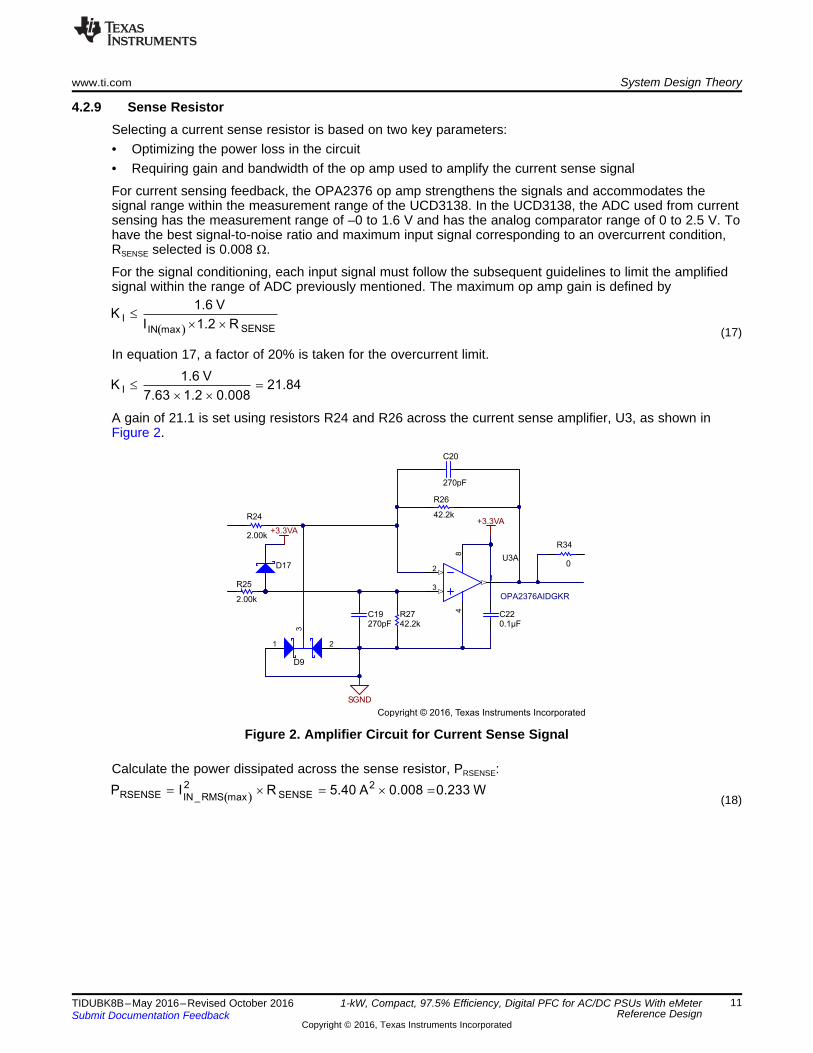
4.2.9 Sense ResistorSelecting a current sense resistor is based on two key parameters:• Optimizing the power loss in the circuit• Requiring gain and bandwidth of the op amp used to amplify the current sense signal
For current sensing feedback, the OPA2376 op amp strengthens the signals and accommodates thesignal range within the measurement range of the UCD3138. In the UCD3138, the ADC used from currentsensing has the measurement range of –0 to 1.6 V and has the analog comparator range of 0 to 2.5 V. Tohave the best signal-to-noise ratio and maximum input signal corresponding to an overcurrent condition,RSENSE selected is 0.008 Ω.
For the signal conditioning, each input signal must follow the subsequent guidelines to limit the amplifiedsignal within the range of ADC previously mentioned. The maximum op amp gain is defined by
(17)
In equation 17, a factor of 20% is taken for the overcurrent limit.
A gain of 21.1 is set using resistors R24 and R26 across the current sense amplifier, U3, as shown inFigure 2.
Figure 2. Amplifier Circuit for Current Sense Signal
Calculate the power dissipated across the sense resistor, PRSENSE:
(18)

REF FB1
FB2 FB1
OUT REF
V R 2.0 VR R 3.07 k
V V 390 V
´= = ´ = W
-
VOUT
2.5 VK 0.00595
420 V£ =
( )VOUT
OUT max
2.5 VK
V£
( ) ( ) ( ) ( ) ( )2 2 2 2
COUT _ 2fline COUT _HFCOUT _RMS totalI I I 1.81 2.43 3.03 A= + = + =
COUT _HF
16 390 VI 2.56 A 1.5 2.43 A
3 1.414 195 V
´
= ´ - =
´ p ´ ´
( )( )
OUTCOUT _HF OUT max
IN_RECTIFIED min
16 VI I 1.5
3 V
´= ´ -
´ p ´
( )OUT max
COUT _ 2fline
I 2.56 AI 1.81 A
2 2= = =
( )OUT min
2.56C 305 µF
2 2 57 0.03 390³ =
p ´ ´ ´ ´ ´
( )( )
OUT
OUT min
RIPPLELINE min
IC
2 2 f V³
p ´ ´ ´ ´
System Design Theory www.ti.com
12 TIDUBK8B–May 2016–Revised October 2016Submit Documentation Feedback
Copyright © 2016, Texas Instruments Incorporated
1-kW, Compact, 97.5% Efficiency, Digital PFC for AC/DC PSUs With eMeterReference Design
4.2.10 Output CapacitorThe output capacitor, COUT, is sized to meet holdup requirements of the converter or the output ripple. Inthis design, the sizes of the output capacitors are based on a voltage ripple of less than 3% of the outputDC voltage.
(19)
Where VRIPPLE = 0.03 × 390 V (assuming 3 % voltage ripple).
The actual capacitor used is 440 μF.
The required ripple current rating at twice the line frequency is equal to:
(20)
There is a high-frequency ripple current through the output capacitor:
(21)
The total ripple current in the output capacitor is the combination of both, and the output capacitor must beselected accordingly:
(22)
4.2.11 Output Voltage Set PointFor low power dissipation and minimal contribution to the voltage set point, 600 kΩ is used for the topvoltage feedback divider resistor, RFB1. Multiple resistors in series are used due to the maximum allowablevoltage across each resistor.
For each input signal to the UCD3138, its magnitude must accommodate the measurement range of thedevice. In the UCD3138, the ADC measurement range is 0 to 2.5 V. To have the best signal-to-noiseratio, the input signal must be as large as possible. For this reason, the signal conditioning for each inputsignal must follow these guidelines:
For VOUT, the voltage divider:
(23)
When the maximum output voltage VOUT(max) is 420-V DC, including the overvoltage protection set at 415-VDC:
Considering these constraints on the gain, the bottom divider resistor, RFB2, is selected to meet thefeedback voltage of 2.0 V at VOUT of 390 V.
(24)
A standard value 3.16-kΩ resistor is selected for RFB2. A 0.1-µF capacitor is added across RFB2 to filterout noise.
www.ti.com System Design Theory
13TIDUBK8B–May 2016–Revised October 2016Submit Documentation Feedback
Copyright © 2016, Texas Instruments Incorporated
1-kW, Compact, 97.5% Efficiency, Digital PFC for AC/DC PSUs With eMeterReference Design
4.3 Bias PowerAn auxiliary housekeeping power supply is needed to power the UCD3138A control circuit, UCC27517Agate driver, and inrush current limiting bypass relay. In addition, external cooling is required when theconverter is operated at power ≥ 900 W. To address each of these needs, an add-on auxiliary powersupply board (TIDA-00708) of 5 W is used. This board is based on a Flyback design using the highvoltage off-line switcher UCC28881. The TIDA-00708 provides a 3.3-V and two 12-V isolated outputs. Formore details, see the TIDA-00708 design guide (TIDUBK7).
Note that the auxiliary power supply TIDA-00708 is already mounted in the TIDA-00707 design and henceis an integral part of TIDA-00707.
Table 3. Expected Auxiliary Power Consumption for Different Devices
DEVICE VOLTAGE (V) MAX CURRENT (mA)UCD3138A controller 3.3 100Relay 12 35Gate driver 12 35Fan (optional) 12 75
4.4 Designing the Firmware on UCD3138A Controller for Single-Phase PFCThe UCD3138 digital power supply controller has multiple peripherals inside the device, which have beenspecifically optimized to enhance the performance of PFC circuit.
A step-by-step guide for the design of the UCD3138A firmware required for the TIDA-00707 PFC isexplained in the PMP10804 test results (TIDUAY4). This document covers the hardware interface, voltageloop and current loop implementation, system protection, firmware structure, internal state machines, andother advanced features. A graphical user interface (GUI) and a guide for tuning the coefficients of a PFCsystem are also presented in the guide.

USB-MiniBLED-Indicator
I/O Port Ribbon Cable
Getting Started Firmware www.ti.com
14 TIDUBK8B–May 2016–Revised October 2016Submit Documentation Feedback
Copyright © 2016, Texas Instruments Incorporated
1-kW, Compact, 97.5% Efficiency, Digital PFC for AC/DC PSUs With eMeterReference Design
5 Getting Started FirmwareThis section details the necessary equipment, test setup, and procedure instructions to program theTIDA-00707 board with the provided software.
5.1 Programming the UCD3138AThe design needs the following equipment and necessary files to program the device:• PMBus to USB Interface Adapter Kit (HPA172)
Accessories include:– USB interface adapter– USB cable (5-pin B mini male to Type A male)– Ribbon cable (Socket to socket, 10 pins, 2 headers, polarized)– Four male-to-female interface wires to connect USB interface adapter to connecter J7 on
TIDA-00707 control card
Figure 3. USB Adapter (HPA172) Outlook
• GUI installations file"TI-Fusion-Digital-Power-Designer-2.0.16.exe" or later version
• Firmware fileUCD3138_PFC.x0 file, located in the software package folder path \TIDA-00707_1.0\Debug
• PC operating systemMicrosoft® Windows XP®, or Vista®, or Windows 7®.

www.ti.com Getting Started Firmware
15TIDUBK8B–May 2016–Revised October 2016Submit Documentation Feedback
Copyright © 2016, Texas Instruments Incorporated
1-kW, Compact, 97.5% Efficiency, Digital PFC for AC/DC PSUs With eMeterReference Design
5.1.1 GUI SetupTo use the GUI:1. Find installation file.
The GUI installation file is "TI-Fusion-Digital-Power-Designer-Version-2.0.16.exe" or later version.2. Install the file.
Double click and launch the .exe file to start the installation. Click "Next" all the way through. Whenpresented, click "I accept the agreement" after reading it. Then click "Install".
3. Launch UCD3138 GUI.After the installation, click "Finish" to exit setup; then click "Exit Program". The GUI for the TIDA-00707board can be launched through the following steps:(a) Click the Windows "Start" button.(b) Click "All Programs".(c) Click "Texas Instruments Fusion Digital Power Designer".(d) Click "Device GUIs".(e) Click "UCD3xxx & UCD9xxx Device GUI".
Figure 4. GUI Launch Path
Getting Started Firmware www.ti.com
16 TIDUBK8B–May 2016–Revised October 2016Submit Documentation Feedback
Copyright © 2016, Texas Instruments Incorporated
1-kW, Compact, 97.5% Efficiency, Digital PFC for AC/DC PSUs With eMeterReference Design
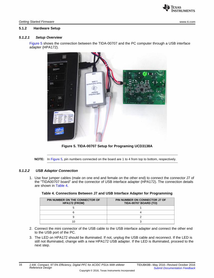
5.1.2 Hardware Setup
5.1.2.1 Setup OverviewFigure 5 shows the connection between the TIDA-00707 and the PC computer through a USB interfaceadapter (HPA172).
Figure 5. TIDA-00707 Setup for Programing UCD3138A
NOTE: In Figure 5, pin numbers connected on the board are 1 to 4 from top to bottom, respectively.
5.1.2.2 USB Adaptor Connection
1. Use four jumper cables (male on one end and female on the other end) to connect the connector J7 ofthe "TIDA00707 board" and the connector of USB interface adapter (HPA172). The connection detailsare shown in Table 4.
Table 4. Connections Between J7 and USB Interface Adapter for Programming
PIN NUMBER ON THE CONNECTOR OFHPA172 (FROM)
PIN NUMBER ON CONNECTOR J7 OFTIDA-00707 BOARD (TO)
5 16 49 210 3
2. Connect the mini connector of the USB cable to the USB interface adapter and connect the other endto the USB port of the PC.
3. The LED on HPA172 should be illuminated. If not, unplug the USB cable and reconnect. If the LED isstill not illuminated, change with a new HPA172 USB adapter. If the LED is illuminated, proceed to thenext step.
www.ti.com Getting Started Firmware
17TIDUBK8B–May 2016–Revised October 2016Submit Documentation Feedback
Copyright © 2016, Texas Instruments Incorporated
1-kW, Compact, 97.5% Efficiency, Digital PFC for AC/DC PSUs With eMeterReference Design
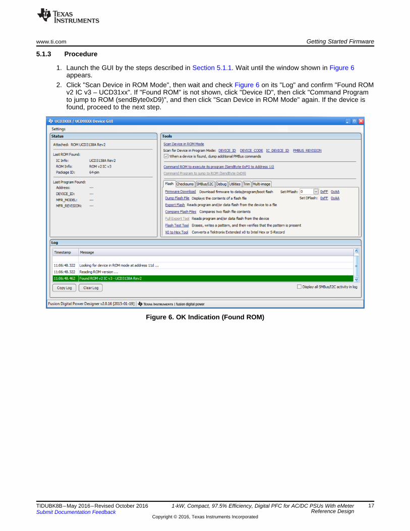
5.1.3 Procedure
1. Launch the GUI by the steps described in Section 5.1.1. Wait until the window shown in Figure 6appears.
2. Click "Scan Device in ROM Mode", then wait and check Figure 6 on its "Log" and confirm "Found ROMv2 IC v3 – UCD31xx". If "Found ROM" is not shown, click "Device ID", then click "Command Programto jump to ROM (sendByte0xD9)", and then click "Scan Device in ROM Mode" again. If the device isfound, proceed to the next step.
Figure 6. OK Indication (Found ROM)

Getting Started Firmware www.ti.com
18 TIDUBK8B–May 2016–Revised October 2016Submit Documentation Feedback
Copyright © 2016, Texas Instruments Incorporated
1-kW, Compact, 97.5% Efficiency, Digital PFC for AC/DC PSUs With eMeterReference Design
3. On the GUI is shown as in Figure 6, click Firmware Download, then a new window appears, as inFigure 7. In this new window:(a) Check "Download data flash". If the “DO NOT write program checksum” radio button is chosen as
shown in Figure 7, the firmware will not be executed once the PFC is powered up. Click "CommandROM to execute its program" to execute the program.If the "Write program checksum" radio button is chosen, the firmware will be executed automaticallyonce the PFC is powered up.
(b) Click "Select file" and find "UCD3138_PFC.x0", which is located in the software package folder path\TIDA-00707_1.0\Debug, and click "Download".
(c) After downloading the program, click "Close" to close the window shown in Figure 7.
Figure 7. Download the Firmware

www.ti.com Getting Started Hardware
19TIDUBK8B–May 2016–Revised October 2016Submit Documentation Feedback
Copyright © 2016, Texas Instruments Incorporated
1-kW, Compact, 97.5% Efficiency, Digital PFC for AC/DC PSUs With eMeterReference Design
6 Getting Started HardwareThis section details the necessary equipment, test setup, and procedure instructions for the TIDA-00707board testing and validation.
6.1 Test ConditionsFor input, the power supply source (VIN) must range from 195-V to 270-V AC. Set the input current limit ofinput AC source to 7.5 A.
For output, use an electronic variable load or a variable resistive load, which must be rated for ≥ 400 Vand must vary the load current from 0 mA to 3 A.
6.2 Test Equipment Required for Board Validation• Isolated AC source• Single-phase power analyzer• Digital oscilloscope• Multimeters• Electronic or resistive load
6.3 Test Procedure
1. Connect input terminals of the reference board to the AC power source.2. Connect output terminals to the electronic load, maintaining correct polarity. VDC and ground pins of
the output are provided as test points. These test points can be removed to make proper solderedconnections for loading the converter for testing.
3. Set and maintain a minimum load of about 10 mA.4. Increase gradually the input voltage from 0 V to turn on voltage of 195-V AC.5. Start the load to draw current from the output terminals of the PFC.6. Observe startup conditions for smooth switching waveforms.7. For a power of ≥ 900 W, an external fan can be used for cooling. A low-wattage, high LFM fan such as
612NMLE is recommended with a 12-V output provided at connector J3. Ensure that the fan is ratedfor 12-V operation and power ≤ 0.75 W.
8. Connect the fan at connector J3, maintaining correct polarity.9. If a low-wattage fan is not available, a cooling fan can be powered from an external DC lab power
supply.

Test Results www.ti.com
20 TIDUBK8B–May 2016–Revised October 2016Submit Documentation Feedback
Copyright © 2016, Texas Instruments Incorporated
1-kW, Compact, 97.5% Efficiency, Digital PFC for AC/DC PSUs With eMeterReference Design
7 Test ResultsThe test results are divided in multiple sections that cover the steady state performance, functionalperformance waveforms and test data, transient performance waveforms, thermal measurements,conducted emission measurements, and Surge and EFT measurements.
7.1 Performance Data
7.1.1 Efficiency and Regulation With Load VariationTable 5 shows the data at a 230-V AC input:
Table 5. Efficiency and Regulation With Load Variation
VINAC (V) IINAC (A) PF PINAC (W) iTHD (%) VOUT (V) IOUT (A) POUT (W) EFF (%) % REG230 0.23 0.80 41.5 13.59 390.8 0.10 37.1 89.4 0.07230 0.37 0.94 79.6 12.90 390.7 0.19 74.6 93.7 0.04230 0.70 0.97 156.2 12.12 390.7 0.38 149.2 95.6 0.04230 1.03 0.99 233.4 9.50 391.0 0.58 224.8 96.3 0.12230 1.36 0.99 309.7 7.00 390.9 0.77 299.4 96.7 0.10230 1.69 0.99 386.6 2.96 390.9 0.96 374.5 96.9 0.10230 2.02 1.00 462.7 2.30 390.8 1.15 449.0 97.0 0.07230 2.35 1.00 539.4 2.00 390.8 1.34 524.1 97.2 0.07230 2.68 1.00 615.7 1.99 390.8 1.53 598.7 97.2 0.07230 3.02 1.00 694.0 1.85 390.7 1.73 674.7 97.2 0.04230 3.35 1.00 770.2 1.72 390.5 1.92 748.2 97.1 –0.01230 3.68 1.00 847.1 1.58 390.4 2.11 822.2 97.1 –0.03230 4.01 1.00 923.0 1.41 390.1 2.30 895.7 97.0 –0.11230 4.20 1.00 997.1 1.43 390.0 2.48 967.2 97.0 –0.15230 4.50 1.00 1034.0 1.40 390.0 2.57 1002.6 97.0 –0.16
7.1.2 Standby PowerThe standby power was noted at multiple AC input voltages with a constant negligible load on the outputDC bus. The results are tabulated in Table 6:
Table 6. No Load Power Consumption
VINAC (VAC) ENERGY INPUT AFTER3 MIN (mWh) VOUT (V) IOUT (A) POUT (W) NO LOAD INPUT
POWER (W)195 113.0 392 0.0 0.0 2.26230 106.0 392 0.0 0.0 2.12270 96.0 392 0.0 0.0 1.92
No load power is contributed by three main branches:• Resistors used input AC voltage sensing• Resistors used for output DC bus voltage sensing• Power consumed by controller and relay
The power consumed by AC input and DC output sensing resistors is ~0.55 W, and this can be decreasedby increasing the resistor values.

Load Current (A)
Pow
er F
acto
r
0.00 0.50 1.00 1.50 2.00 2.50 2.750.80
0.85
0.90
0.95
1.00
1.05
D003
195-V AC230-V AC270-V AC
Load Current (A)
TH
D
0.00 0.50 1.00 1.50 2.00 2.50 2.750
5%
10%
15%
20%
25%
D002
195-V AC230-V AC270-V AC
Load Current (A)
Effi
cien
cy
0.00 0.50 1.00 1.50 2.00 2.50 2.7588%
89%
90%
91%
92%
93%
94%
95%
96%
97%
98%
D001
195-V AC230-V AC270-V AC
Load Current (A)
Reg
ulat
ion
0.00 0.50 1.00 1.50 2.00 2.50 2.75-0.4%
-0.3%
-0.2%
-0.1%
0
0.1%
0.2%
0.3%
0.4%
D002
195-V AC230-V AC270-V AC
www.ti.com Test Results
21TIDUBK8B–May 2016–Revised October 2016Submit Documentation Feedback
Copyright © 2016, Texas Instruments Incorporated
1-kW, Compact, 97.5% Efficiency, Digital PFC for AC/DC PSUs With eMeterReference Design
7.2 Performance Curves
7.2.1 Efficiency and Power Factor With Load and Line VariationFigure 8 and Figure 9 show the measured efficiency and power factor in the system with AC input voltagevariation.
Figure 8. Efficiency versus Output Load Current (IOUT) Figure 9. Power Factor versus Load Current
7.2.2 Input THD With Load and Line RegulationFigure 10 shows the measured input THD of the system with AC input voltage variation. Figure 11 showsthe measured load regulation of the output with AC input voltage variation.
Figure 10. Input THD Variation With Load Current Figure 11. Output Voltage Variation With Load Currentfor Various AC Input Voltages
Test Results www.ti.com
22 TIDUBK8B–May 2016–Revised October 2016Submit Documentation Feedback
Copyright © 2016, Texas Instruments Incorporated
1-kW, Compact, 97.5% Efficiency, Digital PFC for AC/DC PSUs With eMeterReference Design
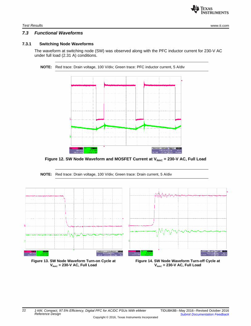
7.3 Functional Waveforms
7.3.1 Switching Node WaveformsThe waveform at switching node (SW) was observed along with the PFC inductor current for 230-V ACunder full load (2.31 A) conditions.
NOTE: Red trace: Drain voltage, 100 V/div; Green trace: PFC inductor current, 5 A/div
Figure 12. SW Node Waveform and MOSFET Current at VINAC = 230-V AC, Full Load
NOTE: Red trace: Drain voltage, 100 V/div; Green trace: Drain current, 5 A/div
Figure 13. SW Node Waveform Turn-on Cycle atVINAC = 230-V AC, Full Load
Figure 14. SW Node Waveform Turn-off Cycle atVINAC = 230-V AC, Full Load

www.ti.com Test Results
23TIDUBK8B–May 2016–Revised October 2016Submit Documentation Feedback
Copyright © 2016, Texas Instruments Incorporated
1-kW, Compact, 97.5% Efficiency, Digital PFC for AC/DC PSUs With eMeterReference Design
7.3.2 Input Voltage and Current WaveformFigure 15 shows the input current waveform at 230-V AC with full load conditions.
Figure 15. Input Voltage and Input Current at VINAC = 230-V AC, Full Load
7.3.3 Inrush Current WaveformInrush current drawn by the system is observed and recorded at a maximum input voltage of 230-V AC.
Figure 16. Output Voltage and Input Inrush Current at VINAC = 230 V, Full Load

Test Results www.ti.com
24 TIDUBK8B–May 2016–Revised October 2016Submit Documentation Feedback
Copyright © 2016, Texas Instruments Incorporated
1-kW, Compact, 97.5% Efficiency, Digital PFC for AC/DC PSUs With eMeterReference Design
7.3.4 Output RippleA ripple observed at the 390-V DC output is loaded to 2.56 A at 230-V AC.
Figure 17. Output Voltage Ripple at VINAC = 230 V,Full Load
Figure 18. Output Voltage Ripple at VINAC = 230 V,Full Load, Only 50-Hz Component
7.3.5 Turn-On CharacteristicsThe 390-V output turn on at full load (2.31 A) was recorded at 230-V AC.
NOTE: Red trace: Output DC bus, 100 V/div; Green trace: Output current, 0.5 A/div.
Figure 19. Output Turn-on Waveform at VINAC = 230 VWith Light Load of 0.5 A
Figure 20. Output Turn-on Waveform at VINAC = 230 VWith Full Load of 2.56 A

www.ti.com Test Results
25TIDUBK8B–May 2016–Revised October 2016Submit Documentation Feedback
Copyright © 2016, Texas Instruments Incorporated
1-kW, Compact, 97.5% Efficiency, Digital PFC for AC/DC PSUs With eMeterReference Design
7.4 Transient Waveforms
7.4.1 Transient Load ResponseLoad transient performance is observed with the load switched at a 0.2-m wire length. The output load isswitched using electronic load.
VIN = 230-V AC, load transient from 0.5 to 2.56 A and vice-versa performance at a 390-V output.
NOTE: Red trace: Output voltage, 20V/div, AC coupling; Green trace:Output current, 1 A/div.
NOTE: Red trace: Output voltage, 20V/div, AC coupling; Green trace:Output current, 1 A/div.
Figure 21. Output Voltage Waveform atVINAC = 230 V, Load Transient From
0.5 to 2.56 A
Figure 22. Output Voltage Waveform atVINAC = 230 V, Load Transient From
2.56 to 0.5 A

Test Results www.ti.com
26 TIDUBK8B–May 2016–Revised October 2016Submit Documentation Feedback
Copyright © 2016, Texas Instruments Incorporated
1-kW, Compact, 97.5% Efficiency, Digital PFC for AC/DC PSUs With eMeterReference Design
7.5 Conducted EmissionsGenerally, conducted emissions increase at full load. This operating point is chosen for measuringconducted EMI.
7.5.1 With Resistive Load at OutputThe 230-V AC input, 2.56-A resistive load is connected to the PSU with short leads. The conductedemissions in a pre-compliance test setup were compared against EN55011 class-A limits and found tomeet them satisfactorily.
Figure 23. Conducted Emissions as per EN55011 Class A

www.ti.com Test Results
27TIDUBK8B–May 2016–Revised October 2016Submit Documentation Feedback
Copyright © 2016, Texas Instruments Incorporated
1-kW, Compact, 97.5% Efficiency, Digital PFC for AC/DC PSUs With eMeterReference Design
7.6 Surge and Fast Transients TestsSurge and EFT testing is done on the boards as per EN55014. The test condition and test results aretabulated in Table 7.
(1) Immunity standard for industrial environments(2) Temporary loss of function or degradation of performance which ceases after the disturbance ceases(3) Normal performance within limits specified by the design or manufacturer
Table 7. Surge and EFT Test Results
BASIC STANDARD PORT IEC 61000-6-2/EN 50082-2REQUIREMENTS (1)
PERFORMANCECRITERION REQUIRED TEST RESULT
IEC/EN 61000-4-4:Fast transients (burst) AC input ±2 kV, 5 kHz B (2) Passed with performance
criterion A (3)
IEC/EN 61000-4-5:Surge AC input ±4 kV line to earth
±2 kV line to line B (2) Passed with performancecriterion A (3)

195 to 265 VAC
GNDE
PGND
390 VDC2.3 Amps max
PGND
0.68µFC1
10.0kR3
275VRV1
DNP
C21
DNP
NOTES:LINE INPUT VOLTAGE: 195VRMS - 265VRMS, 47Hz - 63HzPEAK INPUT CURRENT: 7.0A
OUTPUT VOLTAGE: 390VDC nominalMAXIMUM OUTPUT POWER: 1000W
12V-15VDC
NTC BYPASS CIRCUIT
0.68µFC21
2
3
J1
ED120/3DSVDD
1
GND2
IN+3
IN-4
OUT5
U2UCC27517ADBV
1µFC24
VDCBUS
D3
D1C3D04060A
1
32 Q1
IPP
60R
190P
6
+1
AC2
AC3
-4
BR1
RTN
220 uFC4
PGND
AC_N AC_L
2.00k
R25
2.00k
R24
42.2kR27
1
3
2
D9
SGND
ISENSE_SHUNT
1.00kR29
1.62kR31
SGND
SGND
IIN_SENSE
VDC
VBUS_OV
SGND
VBUS_SENSE
SGND
+3.3VA
1
2
J3
PEC02SAAN
0R39DPWM-1A
+1
2V
1
3
2
48
U3A
OPA2376AIDGKR
7
5
6
48
U3BOPA2376AIDGKR
0.1µFC22
0
R34
200kR8
200kR9
200kR10
200kR12
200kR13
200kR14
3.48kR11
3.48kR15
3.16kR23
3.16kR19
0.01R2
0.04R1
42.2k
R26
1.00k
R30
200kR20
200kR21
200kR22
200kR16
200kR17
200kR18
D17
+3.3VA
100R37
25
413
K1G5LE-1A4 DC12
D13
1µFC25
SGND
Q22N7002-7-F
SGND
1.00k
R35
47.5kR36
SGND
RLY_CTRL
+1
2V
270pF
C20
270pFC19
15A
F1
+3.3VA
1
2
3
HS1
HJ97207
50 Ohm PTC
RCL1
1 234
2.3mH
L3
750343135
67
1
12
5mH
L2744825605
327µH
1 2L1
750343145
2.2nF
C8
2.2nF
C7
2.2nF
C10 2.2nF
C9
1nF
C16
1nF
C15
SGNDSGND
+12V_ISO
SGND1
+3.3VNR+12V
VDCBUS
+12V
PGND
D2
S3J
3.01
R5
2.21
R4
11
22
J4
PBC02SGBN
DNP
11
22
33
44
55
66
J2
PBC06SGBN
DNP
220 uFC5
1µFC3
PGND
DNP
R28DNP
PGND
SGND PGND
Copyright © 2016, Texas Instruments Incorporated
Design Files www.ti.com
28 TIDUBK8B–May 2016–Revised October 2016Submit Documentation Feedback
Copyright © 2016, Texas Instruments Incorporated
1-kW, Compact, 97.5% Efficiency, Digital PFC for AC/DC PSUs With eMeterReference Design
8 Design Files
8.1 SchematicsTo download the schematics, see the design files at TIDA-00707.
Figure 24. Power Stage, Current and Voltage Sensing Schematic

PMBUS-DATA100R47
SGND
PMBUS-CLK
1
3
2
D5
100R49
3.3VD
1.50kR45
1.50kR44
33pFC30
33pFC31
SGND
100R6
1.10kR7
4.75kR33
10kR38
0R42
0.1µFC23
1
23
Q32N7002-7-F
0R43
3.3VD
3.3VD
3.3VD_ISO
3.3VD_ISO
3.3VD_ISO
SGNDISGND
SGND
ISGND
ISGND
SCI-TX1
SCI-RX1
ISO_SCI-TX1
ISO_SCI-RX1
AC_DROP
ISO_SCI-TX1
ISO_SCI-RX1
For PMBUS Communication
For Isolated SCI
33pFC29
/RESET
SCI-TX1
SCI-RX1
1µF
C27
3.3VD
0.1µFC18
10µFC12
1µFC17
SGND
SGND
DPWM-1A
AC_L
PMBUS-DATA
PMBUS-CLK
3.3VD
RLY_CTRL
ISENSE_SHUNT
VBUS_SENSE
ISENSE_SHUNT
VBUS_OV
/RESET
3.3VD
1.65kR48
0.1µF
C32
SGND
SGND
IIN_SENSE
AC_DROP
AC_N
SGND
0.1µF
C28
0.5R40
+3.3VA
+3.3VNR
AGND1
AD132
AD063
AD044
AD035
DGND6
RESET7
ADC_EXT_TRIG/TCAP/SYNC/PWM08
PMBUS_CLK/SCI_TX09
PMBUS_DATA/SCI_RX010
DPWM0A11
DPWM0B12
DPWM1A13
DPWM1B14
DPWM2A15
DPWM2B16
DPWM3A17
DPWM3B18
PMBUS_ALERT19
PMBUS_CTRL20
TCK/TCAP/SYNC/PWM021
TDO/SCI_TX0/PMBUS_ALERT/FAULT022
TDI/SCI_RX0/PMBUS_CTRL/FAULT123
TMS24
FAULT225
DGND26
V33D27
BP1828
AGND29
AGND30
EAP031
EAN032
EAP133
EAN134
EAP235
AGND36
V33A37
AD0038
AD0139
AD0240
PAD41
ANCHOR42
ANCHOR43
ANCHOR44
ANCHOR45
U6
3.3VD
0.1µFC14
0.1µFC11
4.7µFC13
SGND
SGND
+3.3VA
1.00
R32
4.7µFC6
0.1µFC26
+3.3VNR 3.3VD
ISENSE_SHUNT
AC_L
I_SENSE
VBUS_OV
VBUS_SENSEAC_N
ISENSE_SHUNT
3.3
VD
0R46
SGND
ISENSE_SHUNT
1
3
2
D6
+3.3VA
SGND
AC_N AC_LVBUS_OV VBUS_SENSE
1
3
2
D10SGND
+3.3VA
1
3
2
D11SGND
1nF
C36
1nF
C37
+3.3VA
1
3
2
D7SGND
1
3
2
D8SGND
+3.3VA +3.3VA0.1µF
C35
0.1µF
C34
0.027µFC33
SGND
5.11kR50
4
1
2
3
J7
850-10-004-40-001000
5
4
1
2
3
J6
GBC05SBSN-M89
1
2
4
3
U4
1
GND
OUT3
IN2
NC4
NC5
U1
TLV70433DBVT
VCC11
OUTA2
INB3
GND14
GND25
OUTB6
INA7
VCC28
U5
ISO7321CD
Copyright © 2016, Texas Instruments Incorporated
www.ti.com Design Files
29TIDUBK8B–May 2016–Revised October 2016Submit Documentation Feedback
Copyright © 2016, Texas Instruments Incorporated
1-kW, Compact, 97.5% Efficiency, Digital PFC for AC/DC PSUs With eMeterReference Design
Figure 25. Controller and Communication Interface Schematic

Design Files www.ti.com
30 TIDUBK8B–May 2016–Revised October 2016Submit Documentation Feedback
Copyright © 2016, Texas Instruments Incorporated
1-kW, Compact, 97.5% Efficiency, Digital PFC for AC/DC PSUs With eMeterReference Design
8.2 Bill of MaterialsTo download the bill of materials (BOM), see the design files at TIDA-00707.
8.3 PCB Layout RecommendationsA careful PCB layout is critical in a high-current fast-switching circuit to provide appropriate deviceoperation and design robustness. As with all switching power supplies, pay attention to detail in the layoutto save time in troubleshooting later on.
8.3.1 Power Stage Specific GuidelinesFollow these key guidelines to route the power stage components:• Minimize the loop area and trace length of the power path circuits, which contain high frequency
switching currents. This will help reduce EMI and improve the converter’s overall performance.• Keep the switch node as short as possible. A short and optimal trace width helps to reduce induced
ringing caused by parasitic inductance.• Keep traces with high dV/dt potential and high di/dt capability away from or shielded from sensitive
signal traces with adequate clearance and ground shielding.• Keep power ground and control ground separate for each power supply stage. Tie them together (if
they are electrically connected) in one point near DC input return or output return of the given stage.• When multiple capacitors are used in parallel for current sharing, the layout should be symmetrical
across both capacitor leads. If the layout is not identical, the capacitor with the lower series traceimpedance will see higher peak currents and become hotter (i2R).
• Tie the heat sinks of all the power switching components to their respective power grounds.• Place protection devices such as TVS, snubbers, capacitors, or diodes physically close to the device
they are intended to protect, and route with short traces to reduce inductance.• Choose the width of PCB traces based on an acceptable temperature rise at the rated current as per
IPC2152 as well as acceptable DC and AC impedances. The traces should withstand the fault currents(such as short circuit current) before electronic protection devices, such as fuses or circuit breakers,are activated.
• Determine the distances between various traces of the circuit according to the requirements ofapplicable standards. For this design, the UL 60950-1 safety standard is followed to maintain thecreepage and clearance from live line to neutral line and to safety ground, as defined in the Tables 2Kthrough 2N of this standard.
• Adapt the thermal management to fit the end-equipment requirements.

www.ti.com Design Files
31TIDUBK8B–May 2016–Revised October 2016Submit Documentation Feedback
Copyright © 2016, Texas Instruments Incorporated
1-kW, Compact, 97.5% Efficiency, Digital PFC for AC/DC PSUs With eMeterReference Design
8.3.2 UCD3138A Controller Specific GuidelinesThe UCD3138A is a highly integrated controller with a large number of mixed signals. Follow these keyguidelines to route the controller components and signal circuits:• To reduce noise coupling and prevent chip malfunction, group each pin, select good components, have
appropriate connections to each pin, and place well on the PCB.• To avoid chip malfunction, group all digital circuitry and analog circuitry, place digital circuitry close to
each other, place analog circuitry close to each other and make trace connections among them.• Locate all controller support components at specific signal pins close to their connection pin. Connect
the other end of the component to the AGND or DGND, respectively, with shortest trace length.• Find detailed recommendations of each pin connection and its associated component in the
UCD3138A data manual (SLUSC66).• Reference grounds AGND or DGND for the device can be common ground SGND (signal ground) or
separate grounds. In either case, these grounds must be a copper plane or island. If there areseparate AGND or DGND planes, tie them together close to the chip.
• Make the trace routing for the voltage sensing and current sensing circuit components to the device asshort as possible to reduce parasitic effects on the current limit and current and voltage monitoringaccuracy. These traces must not have any coupling to switching signals on the board.
• Connect the SGND plane to high current ground (main power ground) at a single point that is at thenegative terminal of DC IO capacitor, respectively.
8.3.3 Gate Driver Specific GuidelinesFollow these key guidelines to route the high-frequency high-current gate driver:• Locate the driver device as close as possible to the power device to minimize the length of high current
traces between the output pins of gate drive and the gate of the power device.• Locate the VDD bypass capacitors between VDD and GND as close as possible to the driver with
minimal trace length to improve the noise filtering. These capacitors support high-peak current beingdrawn from VDD.
• Minimize the turn-on and turn-off current-loop paths (driver device, power MOSFET, and VDD bypasscapacitor) as much as possible to keep the stray inductance to a minimum.
• Minimize noise coupling with star point grounding from one current loop to another. Connect the driverGND to the other circuit nodes such as the power switch source or the PWM controller ground at onesingle point. The connected paths must be as short as possible to reduce inductance and be as wideas possible to reduce resistance.
8.3.4 Layout PrintsTo download the layer plots, see the design files at TIDA-00707.

Design Files www.ti.com
32 TIDUBK8B–May 2016–Revised October 2016Submit Documentation Feedback
Copyright © 2016, Texas Instruments Incorporated
1-kW, Compact, 97.5% Efficiency, Digital PFC for AC/DC PSUs With eMeterReference Design
8.4 Altium ProjectTo download the Altium project files, see the design files at TIDA-00707.
8.5 Gerber FilesTo download the Gerber files, see the design files at TIDA-00707.
8.6 Assembly DrawingsTo download the assembly drawings, see the design files at TIDA-00707.
9 Software FilesTo download the software files, see the design files at TIDA-00707.
10 References
1. Texas Instruments, High Power Factor and High Efficiency—You Can Have Both, Unitrode PowerSupply Design, Seminar 1800 (SLUP282)
2. Texas Instruments, A Design Review of a Full-Featured 350-W Offline Power Converter, PMP5568Test Results (TIDU186)
3. Texas Instruments, Snubber Circuits: Theory, Design and Applications, Seminar 900, Topic 2(SLUP100)
4. Texas Instruments, Safety Considerations in Power Supply Design, Unitrode Power Supply DesignSeminar, Topic 1 (SLUP224)
5. Texas Instruments, Understanding Noise-Spreading Techniques and their Effects in Switch-ModePower Applications, Unitrode Power Supply Design Seminar, SEM1800, Topic-2 (PDF)
6. Texas Instruments, Designing a UCD3138 Controlled Interleaved PFC, UCD3138 Application Report(SLUA712)
7. Texas Instruments, Designing a UCD3138 Controlled Bridgeless PFC, UCD3138 Application Report(SLUA713)
8. Texas Instruments, UCD3138 Digital Power Peripherals Programmer’s Manual (SLUU995)9. Texas Instruments, PFC THD Reduction and Efficiency Improvement by ZVS or Valley Switching, PFC
Application Report (SLUA644)10. Texas Instruments, Low-cost solution for measuring input power and RMS current, Technical Brief
(SLYT545)11. Texas Instruments, AC cycle skipping improves PFC light-load efficiency, Technical Brief (SLYT585)
11 TerminologySLYZ022 — TI Glossary: This glossary lists and explains terms, acronyms, and definitions.
Specific terms used in the document:
PWM— Pulse width modulation
FETs, MOSFETs—Metal–oxide–semiconductor field-effect transistor
IGBT— Insulated gate bipolar transistor
ESD— Electrostatic discharge
RMS— Root mean square

www.ti.com About the Authors
33TIDUBK8B–May 2016–Revised October 2016Submit Documentation Feedback
Copyright © 2016, Texas Instruments Incorporated
1-kW, Compact, 97.5% Efficiency, Digital PFC for AC/DC PSUs With eMeterReference Design
12 About the AuthorsLATIF AMEER BABU is a Systems Architect at Texas Instruments, where he is responsible fordeveloping reference design solutions for the industrial segment. Latif brings to this role his extensiveexperience in power electronics, high frequency DC-DC converter, and analog circuit design. Latif earnedhis master of technology in power electronics and power systems from Indian Institute of Technology,Mumbai; IN. Latif is a member of the Institute of Electrical and Electronics Engineers (IEEE) and has oneUS patent.
BOSHENG SUN is a Systems Engineer at Texas Instruments where he is responsible for systemssolution, firmware design and collateral development for TI’s high voltage power controller products.Bosheng earned a B.S. degree from Tsinghua University, China in 1995, and an M.S. degree fromCleveland State University, Ohio in 2003, both in electrical engineering. Bosheng has three US patents.
KRISHNA DORA is a Systems Engineer at Texas Instruments where he is responsible for developingreference design solutions for the Power Delivery, Industrial Segment. Krishna brings to this role hisextensive experience in high power converters – Solar and UPS. Krishna earned a B.S degree fromAndhra University, India in 2001, and M.Tech degree from IIT Bombay, Mumbai in 2004, both in electricalengineering. He has two US patents in his name.

Revision B History www.ti.com
34 TIDUBK8B–May 2016–Revised October 2016Submit Documentation Feedback
Copyright © 2016, Texas Instruments Incorporated
Revision History
Revision B HistoryNOTE: Page numbers for previous revisions may differ from page numbers in the current version.
Changes from A Revision (May 2016) to B Revision ...................................................................................................... Page
• Changed title from 1-kW, Compact, High Efficiency, Digital PFC Front-End Reference Design for Telecom and ServerPSU ......................................................................................................................................... 1
Revision A History
Changes from Original (April 2016) to A Revision .......................................................................................................... Page
• Changed from preview page............................................................................................................. 1

IMPORTANT NOTICE FOR TI REFERENCE DESIGNS
Texas Instruments Incorporated (‘TI”) reference designs are solely intended to assist designers (“Designer(s)”) who are developing systemsthat incorporate TI products. TI has not conducted any testing other than that specifically described in the published documentation for aparticular reference design.TI’s provision of reference designs and any other technical, applications or design advice, quality characterization, reliability data or otherinformation or services does not expand or otherwise alter TI’s applicable published warranties or warranty disclaimers for TI products, andno additional obligations or liabilities arise from TI providing such reference designs or other items.TI reserves the right to make corrections, enhancements, improvements and other changes to its reference designs and other items.Designer understands and agrees that Designer remains responsible for using its independent analysis, evaluation and judgment indesigning Designer’s systems and products, and has full and exclusive responsibility to assure the safety of its products and compliance ofits products (and of all TI products used in or for such Designer’s products) with all applicable regulations, laws and other applicablerequirements. Designer represents that, with respect to its applications, it has all the necessary expertise to create and implementsafeguards that (1) anticipate dangerous consequences of failures, (2) monitor failures and their consequences, and (3) lessen thelikelihood of failures that might cause harm and take appropriate actions. Designer agrees that prior to using or distributing any systemsthat include TI products, Designer will thoroughly test such systems and the functionality of such TI products as used in such systems.Designer may not use any TI products in life-critical medical equipment unless authorized officers of the parties have executed a specialcontract specifically governing such use. Life-critical medical equipment is medical equipment where failure of such equipment would causeserious bodily injury or death (e.g., life support, pacemakers, defibrillators, heart pumps, neurostimulators, and implantables). Suchequipment includes, without limitation, all medical devices identified by the U.S. Food and Drug Administration as Class III devices andequivalent classifications outside the U.S.Designers are authorized to use, copy and modify any individual TI reference design only in connection with the development of endproducts that include the TI product(s) identified in that reference design. HOWEVER, NO OTHER LICENSE, EXPRESS OR IMPLIED, BYESTOPPEL OR OTHERWISE TO ANY OTHER TI INTELLECTUAL PROPERTY RIGHT, AND NO LICENSE TO ANY TECHNOLOGY ORINTELLECTUAL PROPERTY RIGHT OF TI OR ANY THIRD PARTY IS GRANTED HEREIN, including but not limited to any patent right,copyright, mask work right, or other intellectual property right relating to any combination, machine, or process in which TI products orservices are used. Information published by TI regarding third-party products or services does not constitute a license to use such productsor services, or a warranty or endorsement thereof. Use of the reference design or other items described above may require a license from athird party under the patents or other intellectual property of the third party, or a license from TI under the patents or other intellectualproperty of TI.TI REFERENCE DESIGNS AND OTHER ITEMS DESCRIBED ABOVE ARE PROVIDED “AS IS” AND WITH ALL FAULTS. TI DISCLAIMSALL OTHER WARRANTIES OR REPRESENTATIONS, EXPRESS OR IMPLIED, REGARDING THE REFERENCE DESIGNS OR USE OFTHE REFERENCE DESIGNS, INCLUDING BUT NOT LIMITED TO ACCURACY OR COMPLETENESS, TITLE, ANY EPIDEMIC FAILUREWARRANTY AND ANY IMPLIED WARRANTIES OF MERCHANTABILITY, FITNESS FOR A PARTICULAR PURPOSE, AND NON-INFRINGEMENT OF ANY THIRD PARTY INTELLECTUAL PROPERTY RIGHTS.TI SHALL NOT BE LIABLE FOR AND SHALL NOT DEFEND OR INDEMNIFY DESIGNERS AGAINST ANY CLAIM, INCLUDING BUT NOTLIMITED TO ANY INFRINGEMENT CLAIM THAT RELATES TO OR IS BASED ON ANY COMBINATION OF PRODUCTS ASDESCRIBED IN A TI REFERENCE DESIGN OR OTHERWISE. IN NO EVENT SHALL TI BE LIABLE FOR ANY ACTUAL, DIRECT,SPECIAL, COLLATERAL, INDIRECT, PUNITIVE, INCIDENTAL, CONSEQUENTIAL OR EXEMPLARY DAMAGES IN CONNECTION WITHOR ARISING OUT OF THE REFERENCE DESIGNS OR USE OF THE REFERENCE DESIGNS, AND REGARDLESS OF WHETHER TIHAS BEEN ADVISED OF THE POSSIBILITY OF SUCH DAMAGES.TI’s standard terms of sale for semiconductor products (http://www.ti.com/sc/docs/stdterms.htm) apply to the sale of packaged integratedcircuit products. Additional terms may apply to the use or sale of other types of TI products and services.Designer will fully indemnify TI and its representatives against any damages, costs, losses, and/or liabilities arising out of Designer’s non-compliance with the terms and provisions of this Notice.IMPORTANT NOTICE
Mailing Address: Texas Instruments, Post Office Box 655303, Dallas, Texas 75265Copyright © 2016, Texas Instruments Incorporated