
Line Filter Design of Parallel Interleaved VSCs for High Power Wind Energy Conversion System
18
Aalborg Universitet Line filter design of parallel interleaved VSCs for high power wind energy conversion systems Gohil, Ghanshyamsinh Vijaysinh; Bede, Lorand; Teodorescu, Remus; Kerekes, Tamas; Blaabjerg, Frede Published in: I E E E Transactions on Power Electronics DOI (link to publication from Publisher): 10.1109/TPEL.2015.2394460 Publication date: 2015 Document Version Early version, also known as pre-print Link to publication from Aalborg University Citation for published version (APA): Gohil, G. V., Bede, L., Teodorescu, R., Kerekes, T., & Blaabjerg, F. (2015). Line filter design of parallel interleaved VSCs for high power wind energy conversion systems. I E E E Transactions on Power Electronics, 30(12), 6775 - 6790. DOI: 10.1109/TPEL.2015.2394460 General rights Copyright and moral rights for the publications made accessible in the public portal are retained by the authors and/or other copyright owners and it is a condition of accessing publications that users recognise and abide by the legal requirements associated with these rights. ? Users may download and print one copy of any publication from the public portal for the purpose of private study or research. ? You may not further distribute the material or use it for any profit-making activity or commercial gain ? You may freely distribute the URL identifying the publication in the public portal ? Take down policy If you believe that this document breaches copyright please contact us at [email protected] providing details, and we will remove access to the work immediately and investigate your claim. Downloaded from vbn.aau.dk on: June 25, 2016
Transcript of Line Filter Design of Parallel Interleaved VSCs for High Power Wind Energy Conversion System

Aalborg Universitet
Line filter design of parallel interleaved VSCs for high power wind energy conversionsystemsGohil, Ghanshyamsinh Vijaysinh; Bede, Lorand; Teodorescu, Remus; Kerekes, Tamas;Blaabjerg, FredePublished in:I E E E Transactions on Power Electronics
DOI (link to publication from Publisher):10.1109/TPEL.2015.2394460
Publication date:2015
Document VersionEarly version, also known as pre-print
Link to publication from Aalborg University
Citation for published version (APA):Gohil, G. V., Bede, L., Teodorescu, R., Kerekes, T., & Blaabjerg, F. (2015). Line filter design of parallelinterleaved VSCs for high power wind energy conversion systems. I E E E Transactions on Power Electronics,30(12), 6775 - 6790. DOI: 10.1109/TPEL.2015.2394460
General rightsCopyright and moral rights for the publications made accessible in the public portal are retained by the authors and/or other copyright ownersand it is a condition of accessing publications that users recognise and abide by the legal requirements associated with these rights.
? Users may download and print one copy of any publication from the public portal for the purpose of private study or research. ? You may not further distribute the material or use it for any profit-making activity or commercial gain ? You may freely distribute the URL identifying the publication in the public portal ?
Take down policyIf you believe that this document breaches copyright please contact us at [email protected] providing details, and we will remove access tothe work immediately and investigate your claim.
Downloaded from vbn.aau.dk on: June 25, 2016

Downloaded from vbn.aau.dk.
Aalborg University
Line Filter Design of Parallel Interleaved VSCs for High Power Wind Energy Conversion System
Gohil, Ghanshyamsinh; Bede, Lorand; Teodorescu, Remus; Kerekes, Tamas; Blaabjerg,
Frede
Published in:
IEEE Transactions on Power Electronics
DOI (link to publication from Publisher):
10.1109/TPEL.2015.2394460
Publication date:
July, 2014
Link to publication from Aalborg University - VBN
Suggested citation format:
G. Gohil, L. Bede, R. Teodorescu, T. Kerekes, F. Blaabjerg, "Line Filter Design of Parallel Interleaved VSCs for
High Power Wind Energy Conversion System," IEEE Transactions on Power Electronics, [Online early access]
DOI: 10.1109/TPEL.2015.2394460.
General rights
Copyright and moral rights for the publications made accessible in the public portal are retained by the authors and/or other copyright owners
and it is a condition of accessing publications that users recognize and abide by the legal requirements associated with these rights.
Users may download and print one copy of any publication from the public portal for the purpose of private study or research.
You may not further distribute the material or use it for any profit-making activity or commercial gain.
You may freely distribute the URL identifying the publication in the public portal.
Take down policy
If you believe that this document breaches copyright please contact us at [email protected] providing details, and we will remove access to the
work immediately and investigate your claim.

1
Line Filter Design of Parallel Interleaved VSCs forHigh Power Wind Energy Conversion Systems
Ghanshyamsinh Gohil, Student Member, IEEE, Lorand Bede, Student Member, IEEE,Remus Teodorescu, Fellow, IEEE, Tamas Kerekes, Member, IEEE, and Frede Blaabjerg, Fellow, IEEE
Abstract—The Voltage Source Converters (VSCs) are oftenconnected in parallel in a Wind Energy Conversion System(WECS) to match the high power rating of the modern windturbines. The effect of the interleaved carriers on the harmonicperformance of the parallel connected VSCs is analyzed inthis paper. In order to achieve low switching losses, the 60◦
clamp Discontinuous PulseWidth Modulation (DPWM1) is usedto modulate the VSCs. A step-by-step design procedure of theline filter, which ensures the desired harmonic performanceunder all operating conditions, is presented. The analyticalharmonic solution for the two parallel interleaved VSCs is derivedin order to obtain the worst case voltage magnitude of theindividual harmonic components. The required value of the filteradmittance for the specific harmonic component is obtainedby using the worst case voltage magnitude and the allowableharmonic injection limit. In order to achieve the desired filterperformance with optimal values of the filter parameters, the useof a LC trap branch with the conventional LCL filter is proposed.The expressions for the resonant frequencies of the proposed linefilter are derived and used in the design to selectively choose thevalues of the line filter components. The analysis and designmethodology are also verified experimentally.
Index Terms—Voltage source converters (VSC), parallel, in-terleaving, filter design, trap filter, discontinuous pulse-widthmodulation (DPWM), wind power
I. INTRODUCTION
The power electronics converters play a vital role in inte-grating a wind turbine into the power system [1]. The fullscale power converter is often used in modern Wind EnergyConversion System (WECS) due to its ability to provide thereactive power compensation and a smooth grid connectionfor the entire speed range, and it is generally realized usingthree-phase two-level pulsewidth modulated Voltage SourceConverter (VSC) [2]. The general trend is to use the windturbines with high output power (megawatt scale) [3] and theswitching frequency of the semiconductor devices employedin these systems is often limited [4]. Therefore, large filtersare required in order to meet the stringent power qualityrequirements imposed by the utility [5]. These filters occupysignificant amount of space in the overall system [6]. More-over, considerable losses occur in the filter components andthe overall conversion efficiency is compromised if large filtercomponents are used [4]. They also result in increased costof the overall converter system [7]. Therefore, the filter sizeshould be made as small as possible to achieve efficient,compact and cost-effective WECS system.
Due to the limited power handling capability of the ex-isting semiconductor devices, the two level VSCs are oftenconnected in parallel [8]–[11] to match the high power rating
of the wind turbine. The parallel connected VSCs can beoperated with interleaved carriers to reduce the value of thefilter components [12]–[18]. However, the carrier interleavingresults in common-mode voltage difference across the parallelVSCs. If the conventional three limb three-phase differentialmode inductor is used without any additional circulatingcurrent filter, high common-mode circulating current flowsas there is no high permeability magnetic path availablefor the common-mode flux in the three limb three-phasedifferential mode inductor [19]. Another approach is to usethe single phase inductor, which acts as both the circulatingcurrent filter and the line filter and permits the use of theinterleaved carriers without having any additional circulatingcurrent filter. However, the use of the single phase inductordoes not bring any advantages in terms of size reduction ofthe filter components [20] and a dedicated filter to suppressthe circulating current is often required.
The use of the parallel interleaved VSCs for the active powerfilter application is presented in [13], [14], where a common-mode inductor is employed to suppress the circulating currentand the reduction in the size of the passive components isdemonstrated. A use of Coupled Inductor (CI) for suppressingthe circulating current is presented in [21] and substantial sizereduction of the filter components can be achieved by using theCI over the single phase line inductor solution [20]. However,the control complexity increases as the precise control overthe fundamental frequency circulating current is required inorder to avoid the saturation of the CI [22].
Some of the harmonic components that are present inthe switched output voltage of the individual VSCs can becanceled by using the interleaved carriers. Miller et al. [12]studied the line current harmonic cancellation effect of Nparallel interleaved VSCs. The effects of the PulseWidthModulation (PWM) scheme, the interleaving angle, and themodulation indices on the line current quality are analyzedin [15]. The optimal interleaving angle to improve the linecurrent quality is discussed in [16]. Mao et al. [17] presented ahybrid PWM scheme, involving multiple switching sequencesand different interleaving angles to improve the line currentquality.
The interleaved carriers in the parallel VSCs can reduce thefiltering requirement by phase shifting some of the harmoniccomponents and thus fully or partially cancel their contributionin the line current. Further reduction in the values of the filtercomponents can be achieved by using a high-order filter [23].The LCL filter is an attractive option [24]–[26], and it iscommonly used in the WECS [2]. For the LCL filter, the

2
x1
VSC1
VSC2
x2
Vdc2
Vdc2
O
Lf
MVGrid
Step-up Transformer
PCCZgrid
Transformerleakage inductance
LCL filter with additional trap branch
Lc
Lg
Lt
Ct
Ix,1
Ix,2 Ix
∆Ix
Ix,gx, cap
Cf
Fig. 1. The grid side converter of the WECS, comprised of two parallel VSCs with interleaved carriers, connected to the medium voltage network by usinga step-up transformer. x = {A,B,C}
admittance transfer function is given as
YLCL(s) =Ig(s)
VPWM (s)
∣∣∣∣∣Vg=0
=1
LfLgCf
1
s(s2 + ω2r,LCL)
(1)where Lf is the converter side inductor, Lg is the grid sideinductor, Cf is the filter capacitor, Ig is the grid current, Vgis the grid voltage, and VPWM is the switched voltage of theVSC. The resonant frequency of the LCL filter is given as
ωr,LCL =
√Lf + LgLfLgCf
(2)
Due to the presence of the complex conjugate poles, the roll-off of the high frequency components (higher than the ωr,LCL)is -60 dB/decade. Therefore, the LCL filter offers goodattenuation to the high frequency harmonic components, andit can effectively reduce the differential mode electromagneticinterference (above 150 kHz) [24]. The switched voltages atthe VSC terminals have harmonic components concentratedaround the multiple of the carrier frequency. Due to the limitedswitching capability of the semiconductor devices used inthe high power applications, a fairly high value of the filtercomponents are required for the LCL filter to attenuate themajor harmonic components (first carrier frequency and itssideband harmonics).
The value of the filter components can be reduced by usinga LC trap branch, which is tuned to attenuate the major carrierharmonics and its sideband harmonics. This can be realized byinserting an inductor in series with the capacitor of the LCLfilter [27]. The use of the LC trap branch to attenuate thesideband harmonic components around the carrier frequencyis proposed in [27], [28]. The multiple LC trap branchesare used, to attenuate the carrier harmonic and its sidebandharmonic components around the carrier frequency and itsmultiple, in [29], [30]. The admittance transfer function ofthe line filter with the LC trap branch, commonly known as
trap filter, is given as
Ytrap(s) =
(1
(Lf + Lg) +LfLg
Lt
)s2 + ω2
t
s(s2 + ω2r,trap)
(3)
The resonant frequencies are given as
ωt =1√LtCf
ωr,trap =1√(
LfLg
Lf+Lg+ Lt
)Cf
(4)
where Lt is the inductor inserted in series with the capacitorCf of the LCL filter. From (4), it is evident that the ωr,trapis less than the ωt. Due to the introduction of the complexconjugate zeros, the roll-off of the high frequency components(higher than the ωt) is -20 dB/decade. This leads to a poorattenuation of the high frequency harmonic components. Onthe contrary, the LCL filter offers good attenuation to thehigh frequency harmonic components. Therefore, the LC trapbranch along with the LCL filter can be used to achievethe desired filtering performance (both at the low and thehigh frequency components) with small values of the filtercomponents. The use of such a filter for single VSC ispresented in [31]. However, the high frequency attenuationis compromised due to insertion of the damping resistor inseries with the capacitive branch.
The VSCs are often connected in parallel in the WECSand the use of interleaved carriers to fully or partially cancelthe effect of some of the harmonic frequency components isproposed in this paper. The design procedure of the LCL filterwith additional LC trap branch of two parallel interleavedVSCs is presented. The paper is organized as follows: theoperation of the parallel interleaved VSCs is briefly describedin Section II. The analysis of the proposed high-order linefilter is discussed in Section III and the filter design constraintsalong with the step-by-step design procedure are presented inSection IV. The simulation and the experimental results arefinally presented in Section V to verify the analysis.

3
II. PARALLEL INTERLEAVED VOLTAGE SOURCECONVERTERS
The carrier signals, of the parallel connected VSCs inWECS (shown in the Fig. 1), are interleaved to reduce thevalue of the filter components. The effect of the interleavedcarriers on the operation of the parallel VSCs is analyzed inthis section.
The interleaved operation of the parallel VSCs:1) Improves the line current quality.2) Reduces the switch current ripple of each VSC, provided
the circulating current is suppressed effectively.Therefore, the value of the filter components can be reduced.However, additional inductive filter is required to suppress thecirculating current. A CI is used as a circulating current filter[15], [20]–[22], [32]–[34] due to its effectiveness in suppress-ing the circulating current. Multiple parallel interleaved VSCswith magnetic coupling between the parallel interleaved legsof the corresponding phase can be realized using the followingconfigurations [21]:
1) Whiffletree configuration.2) Cyclic cascade configuration.3) Using a magnetic structure with multiple parallel mag-
netic limbs.In addition to suppress the circulating current, the CI alsoperforms the function of averaging the switched output voltageof the parallel interleaved legs [21]. The values of the linefilter components depend on the magnitude of the individualharmonic component in the average output voltage, which isthe same in all of the above mentioned CI configurations.Therefore, the line filter design can be carried out inde-pendently, without considering the circulating current filterarrangement.
In this paper, the WECS with two parallel interleavedVSCs is considered. However, the line filter design approach,presented in this paper, can be used for any number ofparallel interleaved VSCs. The use of the LC trap branch withthe conventional LCL filter is proposed. The converter sideinductor Lf , the grid side inductor Lg , and the capacitor Cfforms the LCL filter. The series connection of the Lt andCt forms the LC trap branch. The WECS is connected to amedium voltage network by using a step-up transformer. Theleakage inductance of a step-up transformer often ranges from0.04-0.06 pu [35], and it is considered as a part of the gridside inductance Lg .
The interleaving angle of 180◦ is used as it results in optimalharmonic performance at high modulation indices [16]. Theclosed form analytical solution to determine the individualvoltage harmonic components of the pulsewidth modulatedvoltage is derived. Moreover, the relationship between themaximum value of the switch current ripple and the converterside inductor is also obtained in this section.
A. Modulation Scheme
The 60◦ clamp discontinuous PWM (DPWM1) [36] schemeclamps the output terminals of the VSCs to the positive and thenegative terminals of the dc-link for a 60◦ interval each in a
0 30 150 210 330−1
−0.5
0
0.5
1
Reference space vector angle (degree)
Mag
nitu
de(p
u)
Fig. 2. Modulation waveform of 60◦ clamp PWM (DPWM1) scheme withmodulation index M = 1.
T1 T2T0
Ts
VA1O
+Vdc/2
−Vdc/2
VA2O
+Vdc/2
−Vdc/2
−Vdc
VA,diff
T0T2 T1
T1 T2T0T0T2 T1
VA,avg
+Vdc∆λA
λA,c
VA,cap
Fig. 3. The effect of the interleaved carriers. The pole voltages of phase Aof the individual VSCs and their average VA,avg and difference VA,diff aredepicted. The modulation index is M=1, the interleaving angle is 180◦ andthe reference space vector angle is ψ = 45◦.
fundamental cycle, as shown in Fig. 2. The clamping intervalsof 60◦ are arranged around the positive and negative peakof the fundamental reference voltage. For the applications,where the displacement power factor is close to unity, theswitching is avoided when the current through the devices isnear its peak [37]. In addition to the active power, the WECS isalso required to provide reactive power within a power factorrange of 0.95 leading to 0.95 lagging. In this case, the useof the DPWM1 would result in the switching losses reductionup to 45% compared to that of the continuous space vectormodulation [38].
B. Voltage Harmonic Distortion
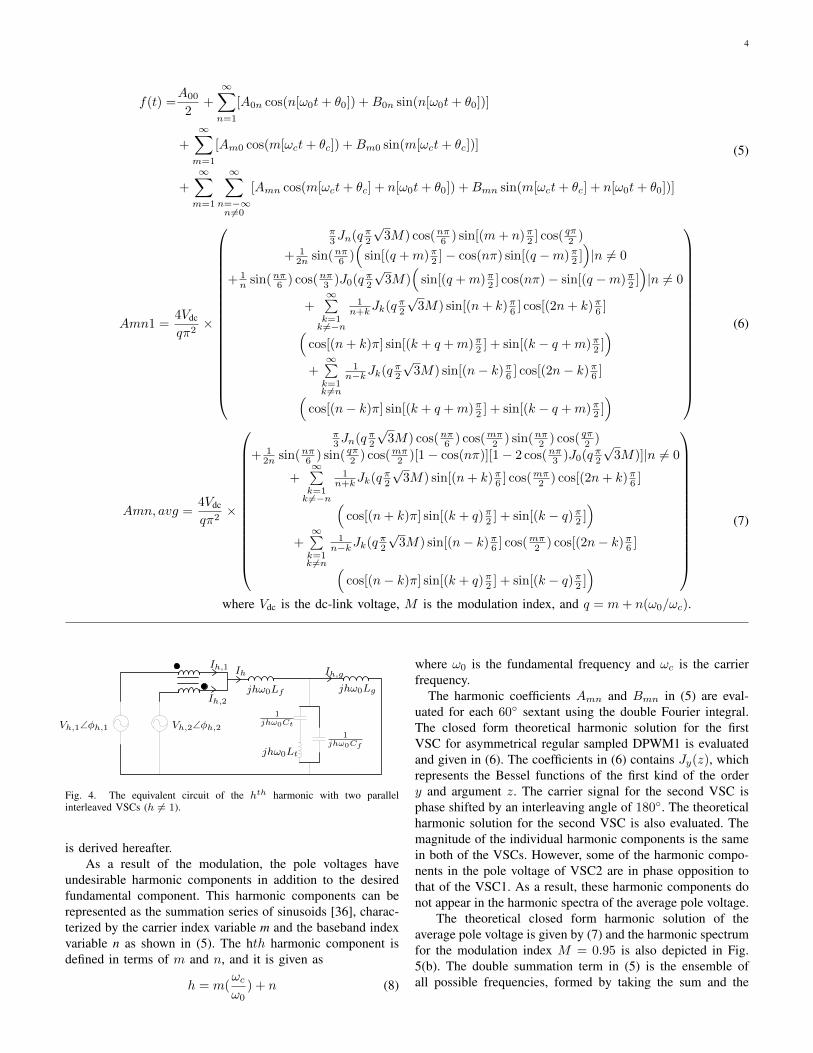
As a result of the interleaved carriers, the pole voltages(measured with respect to the dc-link midpoint O in Fig. 1)of the VSC2 are phase shifted by the interleaving angle withrespect to that of the VSC1. The pole voltages of phase Aof two interleaved VSCs are shown in Fig. 3. The resultantswitched voltage is an average of the individual pole voltages.The difference between the average of the pole voltages andthe grid voltage (VA,avg − VA,g) appears across the line filter,whereas the difference in the pole voltages (VA10 − VA20)is the potential across the circulating current filter Lc. Theequivalent circuit of the hth harmonic component with twoparallel interleaved VSCs is shown in Fig. 4. The harmoniccomponents in the grid current depend on the magnitude of theindividual harmonic components in the average pole voltageand the line filter admittance. Therefore, the magnitude of theindividual harmonics components of the average pole voltage
4
f(t) =A00
2+
∞∑n=1
[A0n cos(n[ω0t+ θ0]) +B0n sin(n[ω0t+ θ0])]
+
∞∑m=1
[Am0 cos(m[ωct+ θc]) +Bm0 sin(m[ωct+ θc])]
+
∞∑m=1
∞∑n=−∞n 6=0
[Amn cos(m[ωct+ θc] + n[ω0t+ θ0]) +Bmn sin(m[ωct+ θc] + n[ω0t+ θ0])]
(5)
Amn1 =4Vdc
qπ2×
π3 Jn(q π2
√3M) cos(nπ6 ) sin[(m+ n)π2 ] cos( qπ2 )
+ 12n sin(nπ6 )
(sin[(q +m)π2 ]− cos(nπ) sin[(q −m)π2 ]
)|n 6= 0
+ 1n sin(nπ6 ) cos(nπ3 )J0(q π2
√3M)
(sin[(q +m)π2 ] cos(nπ)− sin[(q −m)π2 ]
)|n 6= 0
+∞∑k=1k 6=−n
1n+kJk(q π2
√3M) sin[(n+ k)π6 ] cos[(2n+ k)π6 ](
cos[(n+ k)π] sin[(k + q +m)π2 ] + sin[(k − q +m)π2 ])
+∞∑k=1k 6=n
1n−kJk(q π2
√3M) sin[(n− k)π6 ] cos[(2n− k)π6 ](
cos[(n− k)π] sin[(k + q +m)π2 ] + sin[(k − q +m)π2 ])
(6)
Amn, avg =4Vdc
qπ2×
π3 Jn(q π2
√3M) cos(nπ6 ) cos(mπ2 ) sin(nπ2 ) cos( qπ2 )
+ 12n sin(nπ6 ) sin( qπ2 ) cos(mπ2 )[1− cos(nπ)][1− 2 cos(nπ3 )J0(q π2
√3M)]|n 6= 0
+∞∑k=1k 6=−n
1n+kJk(q π2
√3M) sin[(n+ k)π6 ] cos(mπ2 ) cos[(2n+ k)π6 ](
cos[(n+ k)π] sin[(k + q)π2 ] + sin[(k − q)π2 ])
+∞∑k=1k 6=n
1n−kJk(q π2
√3M) sin[(n− k)π6 ] cos(mπ2 ) cos[(2n− k)π6 ](
cos[(n− k)π] sin[(k + q)π2 ] + sin[(k − q)π2 ])
where Vdc is the dc-link voltage, M is the modulation index, and q = m+ n(ω0/ωc).
(7)
Vh,1∠φh,1 Vh,2∠φh,2
jhω0Lf jhω0Lg
jhω0Lt
1jhω0Ct
1jhω0Cf
Ih,1
Ih,2
Ih Ih,g
Fig. 4. The equivalent circuit of the hth harmonic with two parallelinterleaved VSCs (h 6= 1).
is derived hereafter.As a result of the modulation, the pole voltages have
undesirable harmonic components in addition to the desiredfundamental component. This harmonic components can berepresented as the summation series of sinusoids [36], charac-terized by the carrier index variable m and the baseband indexvariable n as shown in (5). The hth harmonic component isdefined in terms of m and n, and it is given as
h = m(ωcω0
) + n (8)
where ω0 is the fundamental frequency and ωc is the carrierfrequency.
The harmonic coefficients Amn and Bmn in (5) are eval-uated for each 60◦ sextant using the double Fourier integral.The closed form theoretical harmonic solution for the firstVSC for asymmetrical regular sampled DPWM1 is evaluatedand given in (6). The coefficients in (6) contains Jy(z), whichrepresents the Bessel functions of the first kind of the ordery and argument z. The carrier signal for the second VSC isphase shifted by an interleaving angle of 180◦. The theoreticalharmonic solution for the second VSC is also evaluated. Themagnitude of the individual harmonic components is the samein both of the VSCs. However, some of the harmonic compo-nents in the pole voltage of VSC2 are in phase opposition tothat of the VSC1. As a result, these harmonic components donot appear in the harmonic spectra of the average pole voltage.
The theoretical closed form harmonic solution of theaverage pole voltage is given by (7) and the harmonic spectrumfor the modulation index M = 0.95 is also depicted in Fig.5(b). The double summation term in (5) is the ensemble ofall possible frequencies, formed by taking the sum and the

5
0 50 100 150 20010−4
10−3
10−2
10−1
100
Harmonic order
Har
mon
icm
agni
tude
(pu)
(a)
0 50 100 150 20010−4
10−3
10−2
10−1
100
Harmonic order
Har
mon
icm
agni
tude
(pu)
(b)
Fig. 5. Theoretical harmonic spectrum with the modulation index m = 0.95and pulse ratio ωc/ω0 = 51. (a) Harmonic spectrum of the pole voltage ofthe individual VSC, (b) Harmonic spectrum of the average pole voltage ofthe interleaved VSCs with an interleaving angle of 180◦.
difference between the carrier harmonics, the fundamentalwaveform and its associated baseband harmonics [36]. Carefulexamination of (7) reveals that the cos(mπ2 ) term appears as amultiplication factor in each summation term. As a result, theharmonic coefficients in (7) are zero for all the odd multipleof the carrier index variable m. Therefore, the side bandharmonics around the odd multiple of the carrier harmonicfrequencies are reduced. This is evident from Fig. 5(b), wherethe pulse ratio is ωc/ω0 =51. The magnitude of the harmoniccomponents around the 51th harmonic and its odd multiple isreduced considerably compared to that of the individual VSC,as shown in Fig. 5. Also the magnitude of all even harmoniccomponents is negligible. This happens due to the presence ofthe sin(nπ2 ) as a multiplication term in the nth order Besselfunction, as given in (7).
C. Switch Current Ripple
The switch current ripple influences the design of both thepassive and the active components. Therefore, the maximumvalue of the peak-to-peak switch current ripple for interleavedVSCs is derived in this subsection. Due to the phase symmetry,only the current through the semiconductor devices of phaseA is analyzed.
Even when the carriers are not interleaved, small circulatingcurrent flows due to the hardware and control asymmetries.
Due to the interleaved carriers, this current further increases.Therefore, the switch currents Ix,1 and Ix,2 have the followingtwo distinct components:
1) The component contributing to the resultant line current2) The circulating current
and the switch current can be given as
Ix,1 = Ix1 + Ix,c
Ix,2 = Ix2 − Ix,c(9)
where, x = phase [A,B,C]. Ix1 and Ix2 are the componentsof the switch currents contributing to the resultant line currentand Ix,c is the circulating current. By neglecting the effect ofthe hardware and the control asymmetries, the line current isassumed to be shared equally between the VSCs (Ix1 = Ix2).From (9), the circulating current can be given as
Ix,c =Ix,1 − Ix,2
2(10)
and the dynamic behavior of the circulating current can bedescribed as
dIx,cdt
=Vx1O − Vx2O
Lc(11)
where Lc is the inductance offered to the circulating current. ACI is used as a circulating current filter due to its effectivenessin suppressing the circulating current. The CI is constructedwithout introducing any intentional air gap in the magnetic fluxpath. As a result, it offers high inductance to the circulatingcurrent and thus the contribution of the circulating currenttowards the switch current can be neglected. This assumptionis also verified by the experimental studies given in section V.
The resultant current Ix is assumed to be shared equallybetween the VSCs and by neglecting the contribution of thecirculating current, the switch current is given as
Ix,1 = Ix,2 uIx2
uIx,f
2+
∆Ix2
(12)
where Ix,f is the fundamental frequency component of theline current and the ∆Ix is the ripple current.
D. Ripple Component of the Resultant Line Current ∆Ix
The switch current ripple is half of the ripple componentof the resultant line current ∆Ix and the relationship betweenthe ∆Ix and Lf is derived in this sub-section. In the interestof brevity, following assumptions are made:
1) The grid voltage is assumed to be free from the harmonicdistortions.
2) The fundamental component of the switch current isassumed to be in phase with the fundamental componentof the reference voltage.
The reference space voltage vector is synthesized using thediscrete voltage vectors such that the volt-second balance ismaintained. The difference between the applied voltage vectorand the reference space vector is known as the error voltagevector, and it is illustrated in Fig. 6. The harmonic fluxvector is a time integral of this error voltage vector, and it

6
ψ
−→V ref
−→V 1 (100)
−→V 2 (110)
d
q
−→V err,2
−→V err,1
−→V err,Z−→
V 0 (000)−→V 7 (111)
Fig. 6. The active and the zero vectors to synthesize a given reference vectorand corresponding error voltage vectors.
T1
d-axis
VSC1VSC2
VSC2: d-axis rippleVSC1: d-axis ripple
Average of the d-axis ripple of the individual VSCs
T7 T1 T7T1 T7 T1T7
Fig. 7. d-axis component of the harmonic flux ripple over a carrier cycleof two parallel VSCs and their average. The interleaving angle is 180◦ andreference space vector angle ψ = 0◦.
is directly proportional to the ripple current [39]–[41]. For theparallel interleaved VSCs, the flux linkage in the converter-side inductor Lf is the average of the harmonic flux vectorsof the individual VSCs.
The harmonic flux vector can be decomposed into d-axisand q-axis components. For the unity power factor operation,the switch current ripple for phase A becomes maximum forthe reference space vector angle ψ = 0◦. At this instant, theripple current of phase A can be obtained by only evaluatingthe d-axis component of the harmonic flux vector, and it isgiven as
−→V derr,1T1 = 2
3Vdc[cosψ − 34M ]T1 (13a)
−→V derr,2T2 = 2
3Vdc[cos(60◦ − ψ)− 34M ]T2 (13b)
−→V derr,zTz = − 1
2VdcMTz (13c)
where T1, T2 and Tz are the dwell time of voltage vectors−→V1,−→V2, and
−→V0/−→V7, respectively. The d-axis component of
the harmonic flux ripple for individual VSCs and their averageflux ripple for ψ = 0◦ are depicted in Fig. 7.
The peak-to-peak value of the resultant d-axis harmonicflux for ψ = 0◦ is given as
λd(pp) =Vdc(1− 3
4M)( 32M − 1)
3fc(14)
This is equal to the peak-to-peak value of the flux linkage inthe Lf and the peak-to-peak current ripple in the Ix is givenas
∆Ix(pp) =Vdc(1− 3
4M)( 32M − 1)
3fcLf(15)
Considering an equal current sharing between the VSCs, thepeak-to-peak value of the switch current ripple is half of the∆Ix(pp). From (15), it is evident that the switch current ripple
Vx,avg(s)
sLf sLg
sLt
1sCt
1sC
Ix(s) Ix,g(s)
Vx,g(s)
Fig. 8. The single phase equivalent circuit of the LCL filter with additionalLC trap branch.
102
103
104
105
106
105
100
Frequency (Hz)
Filteradmittance(S)
Trap lterProposed lter with simpli ed t ransfer funct ionProposed lter with dampingProposed lter, considering the ESR of all the components
t
r 1 r,tr ap
r2
-20 dB/ decade
-60 dB/ decade
Fig. 9. The variation of the magnitude of the admittance transfer function ofthe line filter with frequency.
is the function of a dc-link voltage Vdc, the modulation indexM , and the switching frequency fc. For the given Vdc andfc, the peak-to-peak value of the switch current ripple ismaximum for the modulation index of M = 1, and it is givenas
∆Ix1(pp,max) =Vdc
48fcLf(16)
Once the desired maximum value of the switch current ischosen, the minimum value of the converter side inductanceLf,min can be obtained using (16).
III. LINE FILTER
The line filter arrangement for the parallel interleaved VSCsis shown in Fig. 1 and its single phase equivalent circuit is alsodepicted in Fig. 8. The converter side inductor Lf , the gridside inductor Lg , and the capacitor Cf forms the LCL filter.The series connection of the Lt and Ct forms the LC trapbranch. The Lf and Lg are designed to carry the rated currentand the Equivalent Series Resistance (ESR) of these inductorsare normally small [42] compared to the Lt and its effect inthe low frequency region (upto 9 kHz) can be neglected forthe filter design. The admittance transfer function of the filter(only considering the ESR of the LC trap branch) is givenby (17). The resonant frequencies of the complex conjugatepoles are given by (18). The complex conjugate zeros are alsointroduced due to the presence of the LC trap branch, and it

7
Ix,g(s)
Vx,avg(s)
∣∣∣∣∣Vg=0
=
(1
LfLgC
)s2 + ωt
Qts+ ω2
t
s(s2 + ωr1
Qr1s+ ω2
r1)(s2 + ωr2
Qr2s+ ω2
r2)(17)
ωr1 =1√2
√√√√( 1
LC+
1
LtCeq
)−
√1
LC2
[1
L+
2(Ct − C)
LtCt
]+
1
L2tC
2eq
ωr2 =1√2
√√√√( 1
LC+
1
LtCeq
)+
√1
LC2
[1
L+
2(Ct − C)
LtCt
]+
1
L2tC
2eq
(18)
where L =LfLgLf + Lg
, and Ceq =CCtC + Ct
(19)
is given as
ωt =1√LtCt
(20)
The quality factors are given as
Qt =1
Rt
√LtCt
Qr1 =1
RtCt
1
ωr1
(ω2r2 − ω2
r1)
(ω2r2 − ω2
t )
Qr2 =1
RtCt
1
ωr2
(ω2r2 − ω2
r1)
(ω2t − ω2
r1)
(21)
where Rt is the ESR of the LC trap branch.The variation of the magnitude of the admittance transfer
function of the line filter with respect to the frequency isdepicted in Fig. 9. The magnitude of the simplified admittancetransfer function closely matches with magnitude of the actualfilter transfer function (considering the ESR of all the filtercomponents) in the low frequency region, as shown in Fig.9. The effect of the additional LC trap branch is evident inthe vicinity of the frequency of 2fc, as shown in Fig. 9. Themagnitude of the admittance transfer function of the trap filterproposed in [27], [28] is also plotted in Fig. 9 for comparison.Due to the presence of the capacitive branch C, the line filteroffers a good attenuation to the high frequency components.Therefore, it can effectively reduce the differential modeelectromagnetic interference (above 150 kHz). However, theadditional pole pairs with a resonant frequency ωr2 are presentin the proposed filter, as shown in Fig. 9. The value ofthe resonant frequency ωr1 of the proposed filter is slightlyless than that of the trap filter ωr,trap and it is important toincorporate necessary damping to avoid amplification of theharmonic components, present in close proximity of ωr1. Theparallel Rd/Cd branch is used to provide necessary damping atωr1. However, the introduction of the damping branch slightlyreduces the attenuation offered to the high frequency harmoniccomponents, as shown in Fig. 9.
IV. FILTER DESIGN
The filter is designed for a 2.2 MVA WECS system shownin Fig. 1. The WECS is connected to a medium voltagenetwork using a step-up transformer. The leakage inductance
TABLE IBASE VALUES FOR PER-UNIT SYSTEM
Parameters Base Values (analysis) Base Values (experiments)Power 2.2 MVA (2 MW) 11 kVA (10 kW)Voltage 690 V 400 VCurrent 1840 A 15.87 AFrequency 50 Hz 50 HzInductance 688 µH 46 mHCapacitance 14709 µF 218 µF
of a step-up transformer often ranges from 0.04-0.06 pu [35],and it is considered as a part of the grid side inductance Lg .The analysis and the design methodology are also verified byperforming experiments on a small scale (11 kVA) laboratorysetup. The base values for both of the systems are givenin Table I. The filter design constraints and the step-by-stepdesign procedure are given in this section.
A. Design Constraints
1) Harmonic Current Injection Limits: The harmonic cur-rent injection limit for a generator connected to the medium-voltage network, specified by the German Association ofEnergy and Water Industries (BDEW) [5], [26], [43], isconsidered in this paper. The permissible harmonic currentinjection is determined by the apparent power of the WECSand the Short-Circuit Ratio (SCR) at the Point of the CommonCoupling (PCC). The maximum current injection limit of theindividual harmonic components up to 9 kHz is specified inthe standard and the limits for the WECS connected to the10 KV medium-voltage network are given in Table II. Speciallimits are set for the odd-ordered integer harmonics below the25th harmonic, as given in Table II. The SCR is taken to be20 and the allowable injection limits of individual harmoniccomponents on the low voltage side (690 V) for the 2.2 MVAWECS are calculated. The calculated current injection limitsfor the individual harmonic components are shown in Fig. 10.
2) Maximum Switch Current Ripple: The controllability ofthe system is affected if the switch current has a high ripplecontent [6]. Therefore, the maximum value of the peak-to-peakswitch current ripple is restricted to 0.45 pu in this design.

8
TABLE IIBDEW HARMONIC CURRENT INJECTION LIMITS FOR THE WECS
CONNECTED TO THE 10 KV MEDIUM VOLTAGE NETWORK
Harmonic Order h Current Injection Limit (A/MVA/SCR)5 0.0587 0.08211 0.05213 0.03817 0.02219 0.01823 0.01225 0.01Even-ordered h < 40 0.06 / h40 < h < 180 0.18 / h
20 40 60 80 100 120 140 160 18010−1
100
101
Harmonic order
Har
mon
iccu
rren
tlim
it(A
)
Fig. 10. BDEW [5] harmonic current injection limits for 2.2 MVA WECSon the low voltage side of the transformer with SCR=20.
3) Reactive Power Consumption: The current flowingthrough the semiconductor devices, the converter side filterinductor Lf and the circulating current filter Lc can beminimized by limiting the current drawn by the shunt branchesof the line filter. Moreover, when VSCs are modulated usingDPWM1, the switching losses increase with the increase inthe phase difference between the reference voltage and thefundamental component of the switch current. Therefore, theswitching losses can also be minimized by making the reactivepower consumption of the line filter as small as possible. Thegrid voltage may vary over a range of 1±0.1 pu and thereactive power consumption of the shunt branches of the linefilter is restricted to 0.05 pu for the maximum grid voltage of1.1 pu.
B. Filter Design Procedure
The value of the line filter components are mainly deter-mined based on:
1) The individual voltage harmonic components that appearacross the line filter.
2) The maximum value of the switch current ripple.The magnitude of the individual harmonic frequency compo-nents that appears across the line filter is determined by thedifference of the magnitude of the corresponding harmonicfrequency component in the average of the phase voltagesof the parallel interleaved legs and the magnitude of thesame harmonic frequency component in the grid voltage. Theaverage of the phase voltages of the parallel interleaved legsis independent of the arrangement of the CI. Therefore, the
0 50 100 15010−4
10−3
10−2
10−1
100
Harmonic order
Har
mon
icm
agni
tude
(pu)
M = 0.975
M = 1.025
M = 1.075
VVHS
Fig. 11. The magnitude of the individual voltage harmonic component of theaverage pole voltage.
design of the line filter can be carried out independently.The interleaved operation of the parallel VSCs partially orcompletely eliminates some of the voltage harmonic compo-nents in the average of the phase voltages of the interleavedlegs. Therefore, the reduction in the value of the line filtercomponents can also be achieved. A step-by-step designprocedure for the proposed line filter is illustrated in this sub-section.
1) Virtual Voltage Harmonics: The magnitude of the in-dividual harmonic components in the injected grid current isthe multiplication of the magnitude of the respective harmoniccomponent in the averaged pole voltage and the admittanceoffered by the filter at that harmonic frequency. The theoreticalharmonic solution of the Vx,avg can be obtained using (7).From (7), it is evident that the harmonic coefficients are thefunction of the dc-link voltage Vdc and the modulation indexM . Therefore, for a given value of the dc-link voltage, themagnitude of the individual harmonic components varies withthe modulation index M . The magnitudes of the individ-ual voltage harmonic component of Vx,avg for the differentmodulation indices are shown in Fig. 11. In order to satisfythe harmonic current injection limit over the entire operatingrange, the worst case magnitude of the individual harmoniccomponents of Vx,avg is required. The spectrum comprisesthe maximum values of the individual voltage harmonic com-ponents over the entire operating range and it is defined as aVirtual Voltage Harmonic Spectrum (VVHS) [26].
VVHS for the considered modulation range and the max-imum value of the dc-link voltage is calculated and it isdepicted in Fig. 11. The magnitude of most of the harmoniccomponents (except those harmonic components, which arepresent around the even multiple of the carrier harmonic)increases as the modulation index approaches the lower limit.On the other hand, the harmonic components around the evenmultiple of carrier frequency harmonic increases with increasein the modulation index, as shown in Fig. 11.
2) Required Filter Admittance: The worst case filter ad-mittance requirement is obtained from the harmonic currentinjection limit and the VVHS of the phase voltage. Therequired admittance for the hth harmonic component is given

9
as
Y ∗h =I∗h,BDEWVh,V V HS
(22)
where I∗h,BDEW is the BDEW current injection limit of thehth harmonic component and Vh,V V HS is the voltage mag-nitude of the corresponding harmonic component in VVHSof the phase voltage. The VVHS of the average pole voltagescomprises a common mode component in all phase, which getscanceled out in the line-to-line output voltage. The VVHS ofthe phase voltages is obtained by removing this common modecomponent from the VVHS of average pole voltages.
3) Selection of the LC Trap Branch Parameters: As aresult of the interleaved carriers with an interleaving angle of180◦, the magnitude of the harmonic components around theodd multiple of the carrier frequency is reduced considerably.Therefore, the major voltage harmonic components appeararound the 2nd carrier frequency harmonic (2fc), as shown inFig. 11. The line filter should offer small admittance to theseharmonic components, which can be achieved by tuning theLC trap branch, such that the resonant frequency ωt is equalto 2fc.
The resonant frequency of the LC trap branch is given by(20). The attenuation offered by the filter to the base bandharmonics of the 2nd carrier frequency harmonic depends onthe quality factor of the LC trap branch, given by (21). Themagnitude of the voltage harmonic components in vicinity ofthe 2nd carrier frequency harmonic increases with increasein the modulation index, as shown in Fig. 11. Therefore, therequired value of the quality factor of the LC trap branchstrongly depends on the maximum operating value of themodulation index M .
The capacitors are available in standard values and theselection of the values of the Lt and Ct to realize the requiredvalue of the quality factor is driven by the availability of thecapacitor. The value of Ct is chosen to be 0.02 pu in thisdesign. The value of Lt is taken to be 0.0048 pu in order tohave the resonant frequency of the trap branch at twice theswitching frequency. The quality factor of the trap branchis 25, which is sufficient to achieve the required attenuationaround the 2nd carrier frequency harmonics.
4) Selection of Lf , Lg and C: As a result of an interleavedcarrier, the voltage magnitude of the odd multiple of the carrierharmonics and its side bands is reduced considerably, as shownin Fig. 11. The proposed line filter introduces a resonance atωr1 and ωr2. The damping requirement can be reduced bychoosing the filter parameters such that the resonances occur atthe frequencies where the magnitude of the voltage harmonicsare small.
The values of ωr1 and ωr2 are chosen to be 2.05 kHz and7.65 kHz, respectively. Once the values of ωt, ωr1, and ωr2are decided, the Qr1 and Qr2 are obtained using (21). Fromthese values, the Ceq is calculated, which is given as
Ceq =( 1
Lt
) 1
ω2r1 + ω2
r2 + ωr1ωr2
Qr1Qr2− ω2
r1ω2r2
ω2t
(23)
0 50 100 150
10−2
10−1
100
101
102
Harmonic order
Adm
ittan
ce(S
)
Required filter admittanceα = 2, Lf + Lg = 0.055 puα = 1.25, 5 : Lf + Lg = 0.086 puα = 1.14, 8 : Lf + Lg = 0.126 pu
Fig. 12. Filter admittance plot for different values of α.
For the given values of the ωt, ωr1, and ωr2, the product ofL and C is given as
LC =ω2t
ω2r1ω
2r2
(24)
As the value of Ct is already fixed, the value of C can beobtained using (19) and (23). The desired value of the L canbe achieved by selecting the proper values of Lf and Lg . Manypossible combinations of Lf and Lg exist. Let,
Lg = αL (25)
where α is a constant, and it is greater than one. Using (19)and (25), Lf can be given as
Lf =( α
α− 1
)L (26)
For the given range of grid voltage variation, the maximumvalue of the dc-link voltage, which is required to ensure theVSC operation in a linear modulation range, is decided by thevalue of the inductance (Lf +Lg). Therefore, Lf +Lg shouldbe made as small as possible. The minimum value of Lf +Lgcan be obtained by selecting α = 2, where the values of Lfand Lg are equal. However, from a cost point of view, thiscombination may not be optimal. For α > 2, the value of Lgis more than the value of Lf . The reverse is true for 1 6 α 6 2.The value of α = 2 is taken as the starting point. In case aharmonic injection limit is violated, the design is discardedand a new value of the α will be selected. The maximumvalue of the α is limited by the switch current ripple, and itis given as
αmax =1
1− 48Lfc∆Ix1(pp,max)
Vdc
(27)
In case a harmonic injection limit is violated even with αmax,the design is discarded and new design will be evaluated bychanging the parameters of the LC trap branch. The filteradmittance plot for different values of α is shown in Fig. 12.
As mentioned earlier, appropriate damping is required toavoid amplification of the harmonic components around ωr1and ωr2. Therefore, a Cd/Rd branch has been added. Thecapacitive branch is split into two separate branches and a

10
sLt
1sCt 1
sCfVx,avg(s)
Vg(s)
Rd
Ix(s) Ix,g(s)
sLf sLg
1sCd
C = Cf + Cd
Fig. 13. The single phase equivalent circuit of the LCL filter with additionalLC trap and a Cd/Rd damping branch.
0 0.2 0.4 0.6 0.80
5
10
15
20
β
Freq
uenc
y(k
Hz)
ωr1
ωr2
Fig. 14. Worst case variation in the resonant frequencies as a function of β.
resistor is inserted in one of the branches, as shown in Fig.13. Let,
Cd = βC
Cf + Cd = C(28)
The introduction of the Cd/Rd damping branch changes theresonant frequencies ωr1 and ωr2. The worst case change inthe resonant frequency can be obtained by setting Rd = ∞[44]. The worst case variation in the resonant frequencies asa function of β is shown in Fig. 14. The ωr1 varies in a smallrange, whereas the variation in ωr2 is more and increasessharply as β approaches one. For a given value of Rd, thelosses in the damping branch and admittance offered to thehigh frequency components also increase as β approaches one.In order to restrict the variation in the resonant frequencies ina narrow range and to reduce the inventory [25], β is taken tobe 0.5.
The Cd/Rd damping branch introduces an additional zero(z = −1/CdRd) and a pole (p = z/γ and γ < 1) in theadmittance transfer function of the line filter. The value ofγ can be obtained by solving the denominator polynomial, asgiven in the Appendix. Considering the complexity involved insolving the quintic function, only the information of the addi-tional zero is used to obtain the minimum value of the dampingresistor Rd,min. Once Rd,min is obtained, the required value ofthe damping resistor Rd is determined by using the frequencyresponse characteristic of the filter admittance transfer functiongiven in the Appendix. The improved resonance damping canbe achieved by selecting Rd and Cd such that the |z| < ωr1[44]. Using this relation, the minimum value of the required
0 50 100 15010−3
10−2
10−1
100
101
102
Harmonic order
Adm
ittan
ce(S
)
Required filter admittanceDesigned filterGrid impedance = 0.025 puGrid impedance = 0.05 puGrid impedance = 0.075 pu
Fig. 15. Admittance plot of the designed filter. The effect of the gridinductance variation is also depicted.
Vx,avg
Lf Lg
Vx,gCf
Rd
Cd
Ix Ix,g
Fig. 16. Single phase equivalent circuit of the LCL filter with parallelRd/Cd
damping branch.
damping resistor Rd,min can be obtained, and it is given as
Rd,min =1
ωr1Cd(29)
The line filter is designed by following the above mentionedprocedure. The final filter parameters are given in Table IVand the its admittance plot is also depicted in Fig. 15. Theeffect of the line impedance (Lgrid) variation on the filterperformance is also shown. The value of ωr1 reduces slightlywith the increase in the grid impedance, whereas the ωtremains unaltered.
5) Comparison with the LCL Filter: Reduction in the valueof the filter components is achieved using the proposed highorder filter. This has been verified by comparing the values ofthe filter components of the proposed filter with that of theLCL filter.The single phase equivalent circuit of the LCL filter with
the parallel Rd/Cd damping branch is shown in Fig. 16. Lfis the converter side inductor, Lg is the grid side inductor,and Cf is the filter capacitor. The parameters of the dampingbranch are chosen as per the procedure specified in [6]. Theadmittance transfer function of the LCL filter is given by (1).The value of the filter components of the LCL filter is chosensuch that the filter admittance is less than the required value ofthe filter admittance for the harmonic frequency componentsupto 9 kHz (as per the BDEW limits). The admittance plotof the LCL filter along with the required filter admittance isshown in Fig. 17.The values of the filter components of the designed LCL filterare given in Table III, along with the filter parameters of theproposed filter. The total shunt capacitance (Cf + Cd + Ct)

11
TABLE IIIFILTER PARAMETERS OF THE PROPOSED FILTER AND THE LCL FILTER
Parameters Proposed filter LCL filterLf + Lg 61.92 µH (0.09 pu) 106.75 µH (0.155 pu)Capacitor (Cf + Cd + Ct) 566 µF (0.0386 pu) (Cf + Cd) 2400 µF (0.16 pu)Trap inductor Lt 3.3 µH (0.0048 pu) -
0 50 100 15010−3
10−2
10−1
100
101
102
Harmonic order
Adm
ittan
ce(S
)
Required filter admittanceAdmittance of the designed LCL filter
Fig. 17. Admittance plot of the designed LCL filter, with Lf = 0.065 pu(44.75 µH), Lg = 0.09 pu (62 µH), Cf = 0.08 pu (1200 µF), Cd = 0.08pu (1200 µF).
GPI(s) Gd(s) Gf (s)I∗g V ∗ Ig+ +−
−
Vg
Fig. 18. Grid current controller structure.
in the proposed filter is 0.0386 pu, against the 0.16 pu inthe LCL filter. The reduction in the value of the shuntcapacitor improves the efficiency, as shunt capacitors drawsreactive current and increases resistive losses. In addition, italso increases switching losses when the VSCs are modulatedusing the DPWM1 scheme. The use of the proposed linefilter result in 42 % reduction in the values of the seriesinductors (Lf +Lg). This reduces the volume of the inductivecomponents, as inductors Lf and Lg are designed to carrythe rated value of the current and occupy significant amountof space. The proposed line filter requires an additional trapinductor Lt = 0.0048 pu. However, the value of Lt is verysmall. In addition, Lt is placed in the shunt branch and carriessmall current. Therefore, the volume of this additional inductoris small compared to the reduction achieved in Lf and Lg .
C. Controller Design
The grid current is controlled using the Proportional-Integral(PI) controller, as shown Fig. 18. The control variables aretransformed to a synchronously rotating frame, which rotatesat the fundamental frequency of the grid voltage. The transferfunction of the PI controller is given by
GPI(s) = Kp +Ki
s(30)
TABLE IVPARAMETERS FOR SIMULATION AND EXPERIMENTAL STUDY
Parameters Simulation study ExperimentPower 2.2 MVA (2 MW) 11 kVA (10 kW)Switching frequency 2.55 kHz 2.55 kHzAC voltage (line-to-line) 690 V 400 VDC-link voltage 1080 V 650 VLf 13.76 µH (0.02 pu) 0.87 mH (0.019 pu)Lg (+ Transformer leakage) 48.16 µH (0.07 pu) 3.1 mH (0.0675 pu)Trap capacitor Ct 294 µF (0.02 pu) 4.4 µF (0.02 pu)Trap inductor Lt 3.3 µH (0.0048 pu) 220 µH (0.0048 pu)Capacitor Cf = Cd 136 µF (0.0093 pu) 2 µF (0.0093 pu)
−1 −0.8 −0.6 −0.4 −0.2 0 0.2 0.4 0.6 0.8 1
−1
−0.8
−0.6
−0.4
−0.2
0
0.2
0.4
0.6
0.8
10.4π/T
0.5π/T
0.6π/T
0.7π/T
0.8π/T
0.9π/T
1π/T
0.1π/T
0.2π/T
0.3π/T
0.4π/T
0.5π/T
0.6π/T
0.7π/T
0.8π/T
0.9π/T
1π/T
0.1
0.2
0.3
0.4
0.5
0.6
0.7
0.8
0.9
0.1π/T
0.2π/T
0.3π/T
Root LociDesigned filterGrid impedance = 0.025 puGrid impedance = 0.05 puGrid impedance = 0.075 puGrid impedance = 0.1 pu
Fig. 19. Root loci of the closed loop system with the designed controller.The closed loop poles are marked using ’x’.
where Ki is the integral gain and the Kp is the proportionalgain of the PI controller. The control and PWM delay isrepresented by the Gd(s). The transfer function of the filterGf (s) is given in the Appendix. The parameters of thedesigned filter are given in Table IV. The continuous transferfunctions are discretized and the controller parameters arecalculated in the discrete time domain using the root locustheory. The controller is designed to have a damping factor of0.707. The parameters of the PI controller to meet the givendamping factor requirement are Kp = 0.168 and Ki = 1310.Fig. 19 shows the root locus in the z-plane of the closed-loop

12
0.06 0.07 0.08 0.09 0.1 0.11 0.12 0.13 0.14-3000
-2000
-1000
0
1000
2000
3000
Time (s)
Cur
rent
(A)
IA,gIB,gIC,g
Fig. 20. Step response of the controller. The d-axis current reference ischanged from 0.5 pu to 1 pu at t = 0.1 s.
system with the designed controller parameters.The pole map of the closed-loop system for varying values
of the grid side inductance Lg is also shown in Fig. 19, whereLg is the summation of the leakage inductance of the step-up transformer and the line inductance Lgrid (inductance ofthe electrical network between the PCC and the source). Thevalue of the Lg is varied from 0.07 pu to 0.17 pu. With theincrease in the value of the Lg , the damping factor decreasesfrom 0.707 to 0.5. However, the system remains stable withthe designed PI controller, as evident from Fig. 19.
V. SIMULATION AND EXPERIMENTAL RESULTS
The simulation study and the experimental verification iscarried out to verify the analysis and the design methodologyand the results are presented in this section.
A. Simulation Study
The simulations have been carried out using the PLECS sim-ulation tool. The parameters used for the simulation study aregiven in Table IV. The controller behavior to the step changein the reference signal is shown in Fig. 20. The d-axis currentreference is changed from 0.5 pu to 1 pu. The grid currenttracks the reference and transient performance is also found tobe satisfactory. Fig. 21, shows the simulated waveforms of thesystem, operating under rated conditions with the unity powerfactor operation. The harmonic spectrum of the simulated gridcurrent is obtained by using fast Fourier transform (FFT)and plotted along with the BDEW harmonic current injectionlimit in Fig. 22. The major harmonic components around the2nd carrier harmonic frequency are effectively suppressed.All harmonic components are within the specified harmoniccurrent injection limits.
B. Experimental Results
To verify the analysis and the design methodology, a linefilter for a small scale (11 kVA) laboratory prototype withtwo interleaved VSCs was designed. The parameters of theline filter used in this setup are listed in Table IV. In order toavoid the effect of the background harmonics present in thegrid voltage, an AC power source MX-35 from the CaliforniaInstruments is used as a harmonic free grid emulator. Thegrid impedance is taken to be Zgrid =0.04 pu. The control
0.3 0.31 0.32 0.33 0.34-1500-1000
-5000
50010001500
I A,1
(A)
(a)
0.3 0.31 0.32 0.33 0.34-30-20-10
0102030
I A,c
(A)
(b)
0.3 0.31 0.32 0.33 0.34-3000-2000-1000
0100020003000
I A(A
)(c)
0.3 0.31 0.32 0.33 0.34-1000
-500
0
500
1000C
urre
nt(A
)
(d)
0.3 0.31 0.32 0.33 0.34-600-400-200
0200400600
Cur
rent
(A)
(e)
0.3 0.31 0.32 0.33 0.34-3000-2000-1000
0100020003000
I A,g
(A)
(f)
Fig. 21. Simulated currents of phase A with asymmetrical regular sampledDPWM1 with an interleaving angle of 180◦. (a) VSC1: Phase A current, (b)Circulating current, (c) Resultant current, (d) Current in LC trap branch, (e)Current through the Cf , (f) Grid current.
is implemented using TMS320F28346 floating-point digitalsignal processor.
A 0.6 mH, three phase inductor is used as a converterside inductor. The circulating current filter LC has a leakageinductance of 0.27 mH. Therefore, the total converter sideinductance Lf = 0.87 mH (0.019 pu). A three phase, 10kVA, 1:1 transformer is used. The leakage inductance of this

13
TABLE VMAGNITUDE OF THE CHARACTERISTIC HARMONICS WITH THE TRANSFORMER AND WITH EQUIVALENT INDUCTOR
Harmonic 5th 7th 11th 13th 17th 19th 23rd 25th
With transformer 294 mA 310 mA 67 mA 43 mA 20 mA 26 mA 18 mA 19 mAWith eq. inductor 112 mA 77 mA 12 mA 32 mA 20 mA 17 mA 12 mA 18 mA
0 50 100 15010−3
10−2
10−1
100
101
102
Harmonic order
Cur
rent
(A)
BDEW harmonic current limitsHarmonic components in grid current
Fig. 22. Performance verification of the line filter. The harmonic spectrumof the simulated grid current is depicted.
transformer is measured to be 3.1 mH (0.0675 pu), which isnearly equal to the required value of the 0.07 pu. Therefore,Lg is comprised of the leakage inductance of the transformeronly and an additional inductor is avoided.
The experiment was performed at rated conditions withunity power factor operation. Fig. 23, shows the experimentalwaveforms. The circulating current is effectively suppressedby using CI, as shown in Fig. 23(a). As a result, the effect ofthe circulating current in the individual VSC currents can beconveniently neglected. Therefore IA,1 ≈ IA,2 and the sumof these two currents (IA) is also shown in Fig. 23(a). Themaximum value of the switch current ripple is 0.4 pu againstthe design constraint of 0.45 pu.
The current through the LC trap branch and the capacitivebranch Cf is shown in Fig. 23(b). The LC trap branchprovides low impedance path to the 2nd carrier frequency har-monic and its side bands. Whereas, the capacitive branch Cfsinks the high frequency harmonic components. The injectedcurrent and voltage at the PCC are also shown in Fig. 23(b).The measured grid current had a THD of 3.1 % and the mag-nitude of the individual harmonic component is plotted in Fig.24. The magnitude of all the harmonic frequency componentsof the grid current is lower than the specified BDEW harmoniccurrent injection limits. The major harmonics componentsaround the 2nd carrier harmonic are suppressed effectivelyand the magnitude of these components are also within theprescribed current injection limits. The relative amplitude ofthe harmonic components in the low frequency range is morein the measured grid current than on the simulated grid current.The even order harmonics are mainly present due to theasymmetrical three limb structure of the inductor Lf andthe transformer (Lg). The transformer also draws nonlinearmagnetizing current and increases the magnitude of the odd
IA,1 (10 A/div.)
IA,2 (10 A/div.)
IA,c (2.5 A/div.)
IA (20 A/div.)
(a)
LC trap branch current (5 A/div.)
Current through Cf (5 A/div.)IA,g (25 A/div.)
VA,g (500 V/div.)
(b)
Fig. 23. The experimental results. (a) Ch1: VSC1 phase A current (IA,1),Ch2: VSC2 phase A current (IA,2), Ch3: Circulating current (IA,c), Ch4:Resultant current (IA), (b) Ch1: Current through the LC trap branch, Ch2:Current through the Cf branch, Ch3: Grid current (IA,g), Ch4: Grid voltageat PCC.
order harmonics as well. To validate the filter performance, theexperiment was also performed by replacing the transformerwith a 3.1 mH, three limb inductor. The grid impedance isalso set to zero. The grid current waveform is shown in Fig.25 and the measured grid current had a THD of 1.38 %. Themagnitude of the low order odd harmonic components presentin the grid current is given in Table V and it is compared withthe magnitude of the corresponding harmonic components ofa grid current with a transformer. The magnitude of the loworder harmonic components is significantly smaller with theequivalent inductor than that with the transformer. Therefore,it is concluded that the magnetizing current of the transformersignificantly contributes towards the low order odd harmonic

14
0 20 40 60 80 100 120 140 160 18010−4
10−3
10−2
10−1
100
101
Harmonic order
Cur
rent
(A)
BDEW harmonic current limits (11 kVA)Measured grid current harmonics
Fig. 24. Performance verification of the line filter of the laboratory prototype.
LC trap branch current (5 A/div.)
Current through Cf (5 A/div.)
IA,g (25 A/div.)
VA,g (500 V/div.)
Fig. 25. The experimental results obtained by replacing transformer withequivalent three phase inductor. Ch1: Current through the LC trap branch,Ch2: Current through the Cf branch, Ch3: Grid current (IA,g), Ch4: Gridvoltage.
components of the grid current.
VI. CONCLUSION
A step-by-step design procedure of the line filter for the highpower WECS is presented in this paper. In-depth analysis ofthe effect of the interleaved carriers on the harmonic perfor-mance of the parallel connected VSCs has been made. Theclosed form analytical harmonic solution for the two parallelinterleaved VSCs, modulated by asymmetrical regular sampledDPWM1 scheme, is derived and the reduction in the magni-tude of some of the harmonic components is demonstrated.The effect of the interleaved carriers on the switch currentripple is also analyzed. The set of the worst case individualvoltage harmonic components in the entire operating range(VVHS) is derived, and it is used to obtain the required valueof the filter admittance for each harmonic components. Theadditional LC trap branch with the conventional LCL filter isused. The characteristics of the proposed line filter is analyzedand the design procedure to select the filter parameters, suchthat the filter admittance closely matches with the requiredadmittance at all concerned harmonic frequencies is presented.Although the design example presented in the paper considersDPWM1 as the modulation scheme, the proposed filter design
approach can be equally applicable to other PWM schemesas well. The performance of the filter has been tested. Themagnitude of the individual harmonic components in thegrid current is within the harmonic current injection limits,specified by the BDEW standards.
VII. APPENDIX
Considering the single phase equivalent circuit of the pro-posed filter, as shown in Fig. 13, the admittance transfer ofthe filter is given as
Ix,g(s)
Vx,avg(s)
∣∣∣∣∣Vg=0
= Gs3 +A2s
2 +A1s+A0
s(s5 +B4s4 +B3s3 +B2s2 +B1s+B0)
where
G =
(1
LfLgCf
)A0 =
1
LfCtCdRd, A1 =
1
LtCt+
RtLtCdRd
A2 =RtLt
+1
CdRd
B0 =Lf + Lg
LfLgLtCtCfCdRd, B1 =
Lf + LgLfLgLtCf
( 1
Ct+
RtCdRd
),
B2 =Lf + LgLfLgCf
(RtLt
+1
CdRd
)+Cf + Cd + CtLtCfCtCdRd
B3 =Lf + LgLfLgCf
+Cf + CtLtCfCt
+Rt(Cf + Cd)
LfCfCdRd
B4 =RtLt
+Cf + CdCfCdRd
(31)
ACKNOWLEDGMENT
The authors would like to thank the Intelligent EfficientPower Electronics (IEPE) and the Center of Reliable PowerElectronics (CORPE) for supporting the related research.
REFERENCES
[1] Z. Chen, J. Guerrero, and F. Blaabjerg, “A review of the state of the artof power electronics for wind turbines,” IEEE Trans. Power Electron.,vol. 24, no. 8, pp. 1859–1875, Aug 2009.
[2] F. Blaabjerg, M. Liserre, and K. Ma, “Power electronics converters forwind turbine systems,” IEEE Trans. Ind. Appl., vol. 48, no. 2, pp. 708–719, March 2012.
[3] F. Blaabjerg and K. Ma, “Future on power electronics for wind turbinesystems,” IEEE J. Emerging Sel. Topics Power Electron., vol. 1, no. 3,pp. 139–152, Sept 2013.
[4] H. Zhang and L. Tolbert, “Efficiency impact of silicon carbide powerelectronics for modern wind turbine full scale frequency converter,”IEEE Trans. Ind. Electron., vol. 58, no. 1, pp. 21–28, Jan 2011.
[5] “Technical guidline: Generating plants connected to the medium-voltagenetwork.” BDEW Bundesverband der Energie- und Wasserwirtschafte.V., [Online]. Available: http://www.bdew.de, 2008.
[6] J. Muhlethaler, M. Schweizer, R. Blattmann, J. Kolar, and A. Ecklebe,“Optimal design of LCL harmonic filters for three-phase PFC rectifiers,”IEEE Trans. Power Electron., vol. 28, no. 7, pp. 3114–3125, 2013.
[7] M. Liserre, R. Cardenas, M. Molinas, and J. Rodriguez, “Overview ofmulti-MW wind turbines and wind parks,” IEEE Trans. Ind. Electron.,vol. 58, no. 4, pp. 1081–1095, April 2011.
[8] M. Baumann and J. Kolar, “Parallel connection of two three-phasethree-switch buck-type unity-power-factor rectifier systems with dc-linkcurrent balancing,” IEEE Trans. Ind. Electron., vol. 54, no. 6, pp. 3042–3053, 2007.

15
[9] B. Andresen and J. Birk, “A high power density converter system forthe gamesa G10x 4,5 MW wind turbine,” in Proc. European Conferenceon Power Electronics and Applications, 2007, Sept 2007, pp. 1–8.
[10] J. Birk and B. Andresen, “Parallel-connected converters for optimizingefficiency, reliability and grid harmonics in a wind turbine,” in Proc.European Conference on Power Electronics and Applications, 2007, Sept2007, pp. 1–7.
[11] R. Jones and P. Waite, “Optimised power converter for multi-MW directdrive permanent magnet wind turbines,” in Proc. European Conferenceon Power Electronics and Applications (EPE 2011), Aug 2011, pp. 1–10.
[12] S. Miller, T. Beechner, and J. Sun, “A comprehensive study of harmoniccancellation effects in interleaved three-phase VSCs,” in Proc. IEEEPower Electronics Specialists Conference, 2007. PESC 2007., 2007, pp.29–35.
[13] L. Asimmoaei, E. Aeloiza, J. Kim, P. Enjeti, F. Blaabjerg, L. Moran,and S. Sul, “An interleaved active power filter with reduced size ofpassive components,” in Proc. Twenty-First Annual IEEE Applied PowerElectronics Conference and Exposition, 2006. APEC ’06., 2006, pp. 1–7.
[14] L. Asiminoaei, E. Aeloiza, P. N. Enjeti, and F. Blaabjerg, “Shunt active-power-filter topology based on parallel interleaved inverters,” IEEETrans. Ind. Electron., vol. 55, no. 3, pp. 1175–1189, 2008.
[15] D. Zhang, F. Wang, R. Burgos, L. Rixin, and D. Boroyevich, “Impactof Interleaving on AC Passive Components of Paralleled Three-PhaseVoltage-Source Converters,” IEEE Trans. Ind. Appl., vol. 46, no. 3, pp.1042–1054, 2010.
[16] J. Prasad and G. Narayanan, “Minimization of Grid Current Distortionin Parallel-Connected Converters Through Carrier Interleaving,” IEEETrans. Ind. Electron., vol. 61, no. 1, pp. 76–91, Jan 2014.
[17] X. Mao, A. Jain, and R. Ayyanar, “Hybrid interleaved space vectorPWM for ripple reduction in modular converters,” IEEE Trans. PowerElectron., vol. 26, no. 7, pp. 1954–1967, 2011.
[18] K. Xing, F. Lee, D. Borojevic, Z. Ye, and S. Mazumder, “InterleavedPWM with discontinuous space-vector modulation,” IEEE Trans. PowerElectron., vol. 14, no. 5, pp. 906–917, 1999.
[19] J. Ewanchuk, S. Member, and J. Salmon, “Three-limb Coupled InductorOperation for Voltage Sourced Inverters,” IEEETrans. on Ind. Electron.,vol. 60, no. 5, pp. 1979–1988, 2013.
[20] F. Forest, E. Laboure, T. Meynard, and V. Smet, “Design and comparisonof inductors and intercell transformers for filtering of PWM inverteroutput,” IEEE Trans. Power Electron., vol. 24, no. 3, pp. 812–821, 2009.
[21] I. G. Park and S. I. Kim, “Modeling and analysis of multi-interphasetransformers for connecting power converters in parallel,” in Proc. 28thAnnual IEEE Power Electronics Specialists Conference, 1997. PESC ’97Record., vol. 2, 1997, pp. 1164–1170 vol.2.
[22] B. Cougo, G. Gateau, T. Meynard, M. Bobrowska-Rafal, andM. Cousineau, “PD modulation scheme for three-phase parallel multi-level inverters,” IEEE Trans. Ind. Electron., vol. 59, no. 2, pp. 690–700,2012.
[23] V. Blasko and V. Kaura, “A novel control to actively damp resonance ininput LC filter of a three-phase voltage source converter,” IEEE Trans.Ind. Appl., vol. 33, no. 2, pp. 542–550, Mar 1997.
[24] M. Liserre, F. Blaabjerg, and S. Hansen, “Design and control of an LCL-filter-based three-phase active rectifier,” IEEE Trans. Ind. Appl., vol. 41,no. 5, pp. 1281–1291, Sept 2005.
[25] P. Channegowda and V. John, “Filter optimization for grid interactivevoltage source inverters,” IEEE Trans. Ind. Electron., vol. 57, no. 12,pp. 4106–4114, Dec 2010.
[26] A. Rockhill, M. Liserre, R. Teodorescu, and P. Rodriguez, “Grid-filterdesign for a multimegawatt medium-voltage voltage-source inverter,”IEEE Trans. Ind. Electron., vol. 58, no. 4, pp. 1205–1217, 2011.
[27] W. Wu, Y. He, and F. Blaabjerg, “An LLCL power filter for single-phase grid-tied inverter,” IEEE Trans. Power Electron., vol. 27, no. 2,pp. 782–789, Feb 2012.
[28] Y. Patel, D. Pixler, and A. Nasiri, “Analysis and design of trap andLCL filters for active switching converters,” in Proc. IEEE InternationalSymposium on Industrial Electronics (ISIE), 2010, July 2010, pp. 638–643.
[29] J. Bloemink and T. Green, “Reducing passive filter sizes with tuned trapsfor distribution level power electronics,” in Proc. of the 14th EuropeanConference on Power Electronics and Applications (EPE 2011), Aug2011, pp. 1–9.
[30] J. Xu, J. Yang, J. Ye, Z. Zhang, and A. Shen, “An LTCL filter for three-phase grid-connected converters,” IEEE Trans. Power Electron., vol. 29,no. 8, pp. 4322–4338, Aug 2014.
[31] A. Cantarellas, E. Rakhshani, D. Remon, and P. Rodriguez, “Designof the LCL+trap filter for the two-level VSC installed in a large-scale
wave power plant,” in Proc. Energy Conversion Congress and Exposition(ECCE), 2013 IEEE, Sept 2013, pp. 707–712.
[32] F. Forest, T. Meynard, E. Laboure, V. Costan, E. Sarraute, A. Cuniere,and T. Martire, “Optimization of the supply voltage system in interleavedconverters using intercell transformers,” IEEE Trans. Power Electron.,vol. 22, no. 3, pp. 934–942, 2007.
[33] R. Hausmann and I. Barbi, “Three-phase multilevel bidirectional DC-ACconverter using three-phase coupled inductors,” in Proc. IEEE EnergyConversion Congress and Exposition, 2009. ECCE 2009., Sept 2009,pp. 2160–2167.
[34] B. Cougo, T. Meynard, and G. Gateau, “Parallel Three-Phase Inverters:Optimal PWM Method for Flux Reduction in Intercell Transformers,”IEEE Trans. Power Electron., vol. 26, no. 8, pp. 2184–2191, Aug. 2011.
[35] “Geafol,cast-resin transformers, 100 to 16000 kVA, catalog tv1,”Siemens AG, Power Transmission and Distribution Transformers Di-vision, [Online]. Available: http://www.siemens.com/energy, 2007.
[36] D. G. Holmes and T. A. Lipo, Pulse Width Modulation for PowerConverters: Principles and Practice. Hoboken, NJ: Wiley-IEEE Press,2003.
[37] J. Kolar, H. Ertl, and F. C. Zach, “Influence of the modulation methodon the conduction and switching losses of a PWM converter system,”IEEE Trans. Ind. Appl., vol. 27, no. 6, pp. 1063–1075, 1991.
[38] A. Hava, R. Kerkman, and T. Lipo, “A high-performance generalizeddiscontinuous PWM algorithm,” IEEE Trans. Ind. Appl., vol. 34, no. 5,pp. 1059–1071, 1998.
[39] G. Narayanan and V. T. Ranganathan, “Analytical evaluation of harmonicdistortion in PWM AC drives using the notion of stator flux ripple,” IEEETrans. Power Electron., vol. 20, no. 2, pp. 466–474, 2005.
[40] G. Narayanan, H. Krishnamurthy, D. Zhao, and R. Ayyanar, “Advancedbus-clamping PWM techniquesbased on space vector approach,” IEEETrans. Power Electron., vol. 21, no. 4, pp. 974–984, 2006.
[41] G. Narayanan, V. T. Ranganathan, D. Zhao, H. Krishnamurthy, andR. Ayyanar, “Space vector based hybrid PWM techniques for reducedcurrent ripple,” IEEE Trans. Ind. Electron., vol. 55, no. 4, pp. 1614–1627, 2008.
[42] J. Dannehl, F. Fuchs, S. Hansen, and P. Thgersen, “Investigation of activedamping approaches for pi-based current control of grid-connected pulsewidth modulation converters with lcl filters,” IEEE Trans. Ind. Appl.,vol. 46, no. 4, pp. 1509–1517, July 2010.
[43] S. Araujo, A. Engler, B. Sahan, and F. Antunes, “LCL filter design forgrid-connected NPC inverters in offshore wind turbines,” in Proc. PowerElectronics, 2007. ICPE ’07. 7th Internatonal Conference on, 2007, pp.1133–1138.
[44] W. Wu, Y. He, T. Tang, and F. Blaabjerg, “A new design method forthe passive damped LCL and LLCL filter-based single-phase grid-tiedinverter,” IEEE Trans. Ind. Appl., vol. 60, no. 10, pp. 4339–4350, Oct2013.
Ghanshyamsinh Gohil (S’13) received the M.Tech.degree in electrical engineering with specializationin power electronics and power systems from theIndian Institute of Technology-Bombay, Mumbai,India, in 2011.
He is currently working towards the Ph.D. de-gree at the Department of Energy Technology,Aalborg University, Denmark. Prior to joining thePh.D. studies, he was employed at Siemens Cor-porate Research, Bangalore. His research interestsinclude parallel operation of voltage source convert-
ers, pulsewidth modulation techniques and the design of the inductive powercomponents.

16
Lorand Bede (S’11) was born in Romania in 1989.He received the engineering degree in electricalengineering from Sapientia Hungarian University ofTransilvania, Trgu Mure, Romania, 2011,the MSc.degree in Power Electronics and Drives from Aal-borg University, Aalborg, Denmark, in2013. Cur-rently he is a PhD Fellow at the Departmen t ofEnergy Technology, at Aalborg University,Aalborg.His research interest include grid connected appli-cations based on parallel interleaved converters forwind turbine applications.
Remus Teodorescu (S’94-A’97-M’99-SM’02-F’12)received the Dipl.Ing. degree in electrical engineer-ing from Polytechnical University of Bucharest, Ro-mania in 1989, and PhD. degree in power electronicsfrom University of Galati, Romania, in 1994. In1998, he joined Aalborg University, Department ofEnergy Technology, power electronics section wherehe currently works as full professor. Since 2013he is a visiting professor at Chalmers University.He has coauthored the book Grid Converters forPhotovoltaic and Wind Power Systems, ISBN: 978-
0-470-05751-3, Wiley 2011 and over 200 IEEE journals and conferencepapers. His areas of interests includes: design and control of grid-connectedconverters for photovoltaic and wind power systems, HVDC/FACTS basedon MMC, SiC-based converters, storage systems for utility based on Li-Ionbattery technology. He was the coordinator of the Vestas Power Program 20082013.
Tamas Kerekes (S’06-M’09) obtained his ElectricalEngineer diploma in 2002 from Technical Universityof Cluj, Romania, with specialization in ElectricDrives and Robots. In 2005, he graduated the Masterof Science program at Aalborg University, Instituteof Energy Technology in the field of Power Elec-tronics and Drives. In Sep. 2009 he obtained thePhD degree from the Institute of Energy Technology,Aalborg University. The topic of the PhD programwas: ”Analysis and modeling of transformerless PVinverter systems”. He is currently employed as an
Associate professor and is doing research at the same institute within thefield of grid connected renewable applications. His research interest includegrid connected applications based on DC-DC, DC-AC single- and three-phaseconverter topologies focusing also on switching and conduction loss modelingand minimization in case of Si and new wide-bandgap devices.
Frede Blaabjerg (S’86-M’88-SM’97-F’03) waswith ABB-Scandia, Randers, Denmark, from 1987to 1988. From 1988 to 1992, he was a Ph.D. Studentwith Aalborg University, Aalborg, Denmark. Hebecame an Assistant Professor in 1992, an Asso-ciate Professor in 1996, and a Full Professor ofpower electronics and drives in 1998. His currentresearch interests include power electronics and itsapplications such as in wind turbines, PV systems,reliability, harmonics and adjustable speed drives.He has received 15 IEEE Prize Paper Awards, the
IEEE PELS Distinguished Service Award in 2009, the EPE-PEMC CouncilAward in 2010, the IEEE William E. Newell Power Electronics Award 2014and the Villum Kann Rasmussen Research Award 2014. He was an Editor-in-Chief of the IEEE TRANSACTIONS ON POWER ELECTRONICS from2006 to 2012. He has been Distinguished Lecturer for the IEEE PowerElectronics Society from 2005 to 2007 and for the IEEE Industry ApplicationsSociety from 2010 to 2011. He is nominated in 2014 by Thomson Reuters tobe between the most 250 cited researchers in Engineering in the world.