A wide tuning range Gm-C filter for multi-mode direct-conversion wireless receivers
10
IEEE JOURNAL OF SOLID-STATE CIRCUITS, VOL. 44, NO. 9, SEPTEMBER 2009 2515 A Wide Tuning Range G –C Filter for Multi-Mode CMOS Direct-Conversion Wireless Receivers Tien-Yu Lo, Chung-Chih Hung, Senior Member, IEEE, and Mohammed Ismail, Fellow, IEEE Abstract—A third-order channel selection filter for multi-mode direct-conversion receivers is presented. The filter is designed with a Butterworth prototype and with the target wireless appli- cations of Bluetooth, cdma2000, Wideband CDMA, and IEEE 802.11a/b/g/n wireless LANs. Linear-region MOS transistors are used to perform voltage-to-current conversion. The wide tuning range is achieved by the current multipliers and linear voltage-to-current converters. Implemented in the TSMC 0.18 m CMOS process, the measurement results show that the filter can operate successfully over a cutoff frequency range of 500 kHz to 20 MHz, and is compliant with the requirements of different wire- less applications. The power consumption is 4.1 mW to 11.1 mW for minimum and maximum cutoff frequencies respectively from a 1.2 V supply voltage. The circuit performance compares favorably with previously reported works. Index Terms—Current multiplier, direct-conversion receiver, multi-mode, transconductor, wide tuning range. I. INTRODUCTION A S THE LEVEL of integration in RF transceivers in- creases, CMOS emerges as the technology with the greatest potential for cost effectiveness where RF, mixed-signal and digital circuits are integrated in a single system-on-chip (SoC). This is particularly true when multi-mode wireless chip sets are embedded into mobile computing or multimedia systems. When designing a wireless receiver, one of the most important tasks is to design the channel filtering to separate the desired signal from the unwanted ones. Recent demand for multi-standard transceivers calls for adopting direct-conversion architectures to achieve the highest level of integration and for ease of system design. Fig. 1 shows a block diagram of a direct-conversion receiver. It converts the RF signal with both desired and unwanted signals, directly to baseband. Since the unwanted signals are still left at adjacent channel, the received signal is selected by the channel selection filter for further demodulation. However, an array or a stack of channel selection filters in a multi-standard radio design may not be power-efficient and would need large chip areas. Therefore, Manuscript received November 27, 2007; revised April 11, 2009. Current version published August 26, 2009. T.-Y. Lo is with MediaTek Inc., Hsinchu, Taiwan (e-mail: tienyu.lo@gmail. com). C.-C. Hung is with the Department of Communication Engineering, National Chiao Tung University, Hsinchu, Taiwan (e-mail: [email protected]). M. Ismail is with the Department of Electrical and Computer Engineering, The Ohio State University, Columbus, OH 43210 USA (e-mail: ismail@ece. osu.edu). Color versions of one or more of the figures in this paper are available online at http://ieeexplore.ieee.org. Digital Object Identifier 10.1109/JSSC.2009.2023154 Fig. 1. Simplified block diagram of a direct-conversion receiver. there is a strong motivation to realize a single baseband channel select filter such that it meets the requirements of multi-mode applications. This work focuses on the design of such a multi-mode channel selection filter and is targeting direct-conversion radio architectures. The filter is designed based on a G –C filter topology, and has a wide continuous tuning range. The large tuning range is designed to meet the wireless specifications of Bluetooth (650 kHz), cdma2000 (700 kHz), Wideband CDMA (2.2 MHz), IEEE 802.11a/g (10 MHz), IEEE 802.11b (12 MHz), IEEE 802.11n (20 MHz) wireless LANs applica- tions. These specifications cover the frequency range from 650 kHz to 20 MHz. Most G –C filters encounter noise and linearity tradeoff when they are utilized for large tuning-range application. They usually suffer from either low linearity or high noise. From system level analysis, the input-referred noise within the spec- ified bandwidth can be determined by giving the RF front-end gain. The noise level defines the sensitivity of a receiver where the minimum acceptable level can be detected, and the gain of the RF front-end section should be chosen so that the output stage would not saturate under system specification. From the Friis equation, the noise figure (NF) of the receiver is given by (1) where , and are the noise figure of re- ceiver, RF front-end, and analog baseband. The analog base- band includes the analog filter and the programmable gain am- plifier. When the output impedance of the RF front-end is given by , the input-referred noise of analog baseband section can be expressed as (2) where is the Boltzmann coefficient and is the input-re- ferred noise power specified for 1 Hz bandwidth. Therefore, we can relax required noise specification by giving a larger RF 0018-9200/$26.00 © 2009 IEEE
-
Upload
independent -
Category
Documents
-
view
4 -
download
0
Transcript of A wide tuning range Gm-C filter for multi-mode direct-conversion wireless receivers

IEEE JOURNAL OF SOLID-STATE CIRCUITS, VOL. 44, NO. 9, SEPTEMBER 2009 2515
A Wide Tuning Range G�–C Filter for Multi-ModeCMOS Direct-Conversion Wireless Receivers
Tien-Yu Lo, Chung-Chih Hung, Senior Member, IEEE, and Mohammed Ismail, Fellow, IEEE
Abstract—A third-order channel selection filter for multi-modedirect-conversion receivers is presented. The filter is designedwith a Butterworth prototype and with the target wireless appli-cations of Bluetooth, cdma2000, Wideband CDMA, and IEEE802.11a/b/g/n wireless LANs. Linear-region MOS transistorsare used to perform voltage-to-current conversion. The widetuning range is achieved by the current multipliers and linearvoltage-to-current converters. Implemented in the TSMC 0.18 mCMOS process, the measurement results show that the filter canoperate successfully over a cutoff frequency range of 500 kHz to20 MHz, and is compliant with the requirements of different wire-less applications. The power consumption is 4.1 mW to 11.1 mWfor minimum and maximum cutoff frequencies respectively from a1.2 V supply voltage. The circuit performance compares favorablywith previously reported works.
Index Terms—Current multiplier, direct-conversion receiver,multi-mode, transconductor, wide tuning range.
I. INTRODUCTION
A S THE LEVEL of integration in RF transceivers in-creases, CMOS emerges as the technology with the
greatest potential for cost effectiveness where RF, mixed-signaland digital circuits are integrated in a single system-on-chip(SoC). This is particularly true when multi-mode wirelesschip sets are embedded into mobile computing or multimediasystems. When designing a wireless receiver, one of the mostimportant tasks is to design the channel filtering to separatethe desired signal from the unwanted ones. Recent demand formulti-standard transceivers calls for adopting direct-conversionarchitectures to achieve the highest level of integration andfor ease of system design. Fig. 1 shows a block diagram ofa direct-conversion receiver. It converts the RF signal withboth desired and unwanted signals, directly to baseband. Sincethe unwanted signals are still left at adjacent channel, thereceived signal is selected by the channel selection filter forfurther demodulation. However, an array or a stack of channelselection filters in a multi-standard radio design may not bepower-efficient and would need large chip areas. Therefore,
Manuscript received November 27, 2007; revised April 11, 2009. Currentversion published August 26, 2009.
T.-Y. Lo is with MediaTek Inc., Hsinchu, Taiwan (e-mail: [email protected]).
C.-C. Hung is with the Department of Communication Engineering, NationalChiao Tung University, Hsinchu, Taiwan (e-mail: [email protected]).
M. Ismail is with the Department of Electrical and Computer Engineering,The Ohio State University, Columbus, OH 43210 USA (e-mail: [email protected]).
Color versions of one or more of the figures in this paper are available onlineat http://ieeexplore.ieee.org.
Digital Object Identifier 10.1109/JSSC.2009.2023154
Fig. 1. Simplified block diagram of a direct-conversion receiver.
there is a strong motivation to realize a single baseband channelselect filter such that it meets the requirements of multi-modeapplications.
This work focuses on the design of such a multi-modechannel selection filter and is targeting direct-conversion radioarchitectures. The filter is designed based on a G –C filtertopology, and has a wide continuous tuning range. The largetuning range is designed to meet the wireless specificationsof Bluetooth (650 kHz), cdma2000 (700 kHz), WidebandCDMA (2.2 MHz), IEEE 802.11a/g (10 MHz), IEEE 802.11b(12 MHz), IEEE 802.11n (20 MHz) wireless LANs applica-tions. These specifications cover the frequency range from650 kHz to 20 MHz.
Most G –C filters encounter noise and linearity tradeoffwhen they are utilized for large tuning-range application. Theyusually suffer from either low linearity or high noise. Fromsystem level analysis, the input-referred noise within the spec-ified bandwidth can be determined by giving the RF front-endgain. The noise level defines the sensitivity of a receiver wherethe minimum acceptable level can be detected, and the gain ofthe RF front-end section should be chosen so that the outputstage would not saturate under system specification. From theFriis equation, the noise figure (NF) of the receiver is given by
(1)
where , and are the noise figure of re-ceiver, RF front-end, and analog baseband. The analog base-band includes the analog filter and the programmable gain am-plifier. When the output impedance of the RF front-end is givenby , the input-referred noise of analog baseband sectioncan be expressed as
(2)
where is the Boltzmann coefficient and is the input-re-ferred noise power specified for 1 Hz bandwidth. Therefore,we can relax required noise specification by giving a larger RF
0018-9200/$26.00 © 2009 IEEE

2516 IEEE JOURNAL OF SOLID-STATE CIRCUITS, VOL. 44, NO. 9, SEPTEMBER 2009
front-end gain. However, we should note that the linearity per-formance is defined by
(3)
where , and are the input third-orderintercept point (IIP3) of the system, RF front-end, and analogbaseband sections. It is clearly shown that larger RF front-endgain will amplifier blockers and relax the noise performance ofthe baseband section. To define the noise specification in thesystem design, the RF front-end gain can be obtained by givinglargest blocker in RF front-end stage, and can be enlarged bypushing the linearity requirement to the baseband stage. Then,the noise specification of the baseband stage can be relaxed. Theanalysis for a multi-mode receiver front-end requires a range ofinput signal magnitude specifications that cover all the operationmodes. Assuming that the receiver provides a NF of 9 dB, anoverall IIP3 of 9 dBm, and a gain requirement between 10 and100 dB, the range of all the requirements for the baseband sec-tion is the result of an optimal tradeoff among gain, noise, andlinearity throughout the receiver blocks. By giving the systemanalysis and the scenario simulated over the receiver, the ac-ceptable levels of the filter IIP3 for GSM/cdam2000, WidebandCDMA, and IEEE 802.11 mode are 19.2 Bm, 21.1 dBm, and19.6 dBm, respectively.
For the G –C topology, a transconductor is used as a basicbuilding block [1]–[5], and the transconductance value is pro-portional to the 3 dB cutoff frequency of the filter. The ap-plication mode is selected by changing the transconductance,and a tuning ratio of 30 is required. However, when process andtemperature variations are taken into account, a tuning ratio ofmore than 50 should be achieved and the linearity performanceshould be still maintained at acceptable levels.
In this paper, Section II develops the proposed high linearitytransconductor with a wide transconductance tuning range. Thethird-order Butterworth G –C filter which meets the requiredspecification is presented in Section III. Section IV presents themeasurement results and compares the proposed design with thestate of the art. Finally, conclusions are addressed in Section V.
II. PROPOSED TRANSCONDUCTOR CIRCUIT
The main function of a transconductor is to convert the inputvoltage into the output current with a linear transformationfactor, and the transconductor employed in filters must belinear over the input signal swing range. On the other hand, thetransconductance should be tuned to compensate for processand temperature variations, and we can model it as a voltagecontrolled current source. In the circuit implementation, bipolartransistors offer wide transconductance tunable range becausethe collector current can be varied with little change in thebase-emitter voltage. In contrast, the bias of the MOS transis-tors should be varied significantly and the supply voltage wouldthen limit the tuning range, which implies the requirement of ahigher supply voltage. Thus, a high linearity and wide tuningrange transconductor in a low voltage CMOS technology wouldnot only be needed for multi-mode wireless applications butalso be helpful to combine with digital circuits for a system ona chip design.
A. The Voltage-to-Current Conversion in CMOS Technology
Fig. 2(a) shows a conventional transconductor, where thevoltage-to-current conversion is obtained by using an opera-tional amplifier through a passive resistor. The current is thensensed and mirrored to the output node. In this circuit, an arrayof resistors should be used to make the transconductance tun-able. This method will increase the chip area and the precisionof the transconductance would be limited by the choice of theprogrammable resistors. To achieve transconductance tuning,a single linear region transistor, shown in Fig. 2(b), is used toreplace the passive resistor. This circuit is a MOSFET-onlyconfiguration. When the NMOS operates in the linear region, alinear drain current is obtained, and a linear voltage-to-currentrelationship for the circuit in Fig. 2(b) is presumably obtained.From a simplified BISM Level 3 model, the drain current isgiven by
where (4)
where is the body effect factor and is the surface inversionpotential. , and are the width andlength of the device, respectively, is the oxide capacitanceper unit channel area, is the low-field mobility, andis the NMOS threshold voltage. and are the gate-to-source and drain-to-source voltages, respectively. By taking theprocess and temperature variation into consideration, can bechosen to be a value of 1.2.
We can now see that the output current would not really holda linear relationship to the input voltage owing to the additionalsecond term in (4), which thus degrades the linearity of thetransconductor. We can find that the second term in (4) formsa square-law equation. Previous research [6] reports that an-other transistor could be added to cancel out the second termin (4) based on the large signal square-law equation in the sat-uration region. Thus, the output current would be proportionalto the input voltage, and the transconductance can be tuned byadjusting the bias voltage at the gate terminal. In the circuit, the
40 dB total harmonic distortion (THD) was reported. Thereare several disadvantages of this linearization technique. First,extra complex circuit should be included for current cancella-tion, and this technique needs an extra operational amplifier,which implies more power consumption. Second, the constraintof linear region operation, , should be held andthis condition is hard to sustain under wide tuning requirement.Finally, it would not work well in modern nanoscale CMOStechnologies owing to the fact that short channel effects wouldalter the square-law behavior and then degrades nonlinearitycancellation.
Since the compensation technique reported in [6] is based ona single-ended structure and is not suitable to provide the re-quired high linearity and low power for transconductor designin modern CMOS process, a differential structure can be simplyused to cancel out the second term in (4). Therefore, we can takethe single-ended circuit of Fig. 2(b) and use it in a fully differen-tial mode as shown in Fig. 2(c). To obtain the voltage-to-current

LO et al.: A WIDE TUNING RANGE G –C FILTER FOR MULTI-MODE CMOS DIRECT-CONVERSION WIRELESS RECEIVERS 2517
Fig. 2. (a) Conventional transconductor. (b) MOSFET-only transconductor. (c) Differential transconductor.
characteristics of the circuit, the input differential voltages at thegate of transistors M1 and M2, are given by
(5)
(6)
where is the input common-mode voltage and is theinput differential voltage. The gate terminals of the linear-regiontransistors M7 and M8 will be biased at an appropriate voltage,
, to make sure the linear region operation is achieved. Thesecond term in (4) can be cancelled out by the inherent differ-ential structure, and thus the output current would be given by
(7)
The equation shows that a linear voltage-to-current conversionis obtained, and that the output current is dependent on the biasvoltage and the input common-mode voltage.
B. The Proposed Transconductor With Tuning Scheme
Followed the basic concept of the differential structure inFig. 2(c), wide range transconductance tuning is hard to achieveby adjusting and . In general, should be biasedat a higher voltage, such as the supply rail, and then the tran-sistor would always work in deep linear region and perform ahighly linear operation. Thus, a high linearity current multiplierwould be required following the voltage-to-current conversion.
Fig. 3 shows the concept of the transconductor, which has awide transconductance range. In the proposed transconductor,the linear voltage-to-current conversion is performed first, andthen the transconductance is tuned over a wide range using thetranslinear loop that follows. The translinear loop is to pro-vide the function of current multiplier. Through the use of thefeedback loop, linear voltage-to-current conversion can be ob-tained owing to the fact that the input voltage would be equalto the drain voltage of transistors M1 and M2. Thus, the currentflowing through resistors and would have a very highlinearity relationship with the input voltage. The current multi-plier is composed by transistors M1 to M4, resistors and
Fig. 3. Concept of a wide tuning range transconductor.
, and current source . Transistors M1 to M4 are biasedto operate in the weak inversion region while suitable devicesizes are used. A single expression of the transistor model usefulin weak, moderate, and strong inversion regions with largerthan a few times of the thermal voltage , is employed [7]
(8)
where is the fitting parameter, is the subthreshold slopefactor, is the transistor threshold voltage, and is thethermal voltage. The inversion factor defined by isoften used to define the boundaries between the MOS inversionregions. When , the operation region is corresponding tothe strong inversion. On the opposite, the operation region is cor-responding to the weak inversion when . The expressioncan fit the case of the general weak to strong inversion equa-tions. For a MOSFET operating in the weak inversion region,its current exhibits an exponential dependence on , and canbe expressed from (8) to obtain
(9)

2518 IEEE JOURNAL OF SOLID-STATE CIRCUITS, VOL. 44, NO. 9, SEPTEMBER 2009
where and are the width and the length of the transistor,respectively, and is the reverse saturation current. From theabove equation, we can find that
(10)
(11)
The device sizes of transistors M1 and M2 are set to be thesame, and so are transistors M3 and M4. We can obtain fromthe linear conversion, and , where
. We can have
(12)
The current output from the differential pair of transistors M3and M4 can be expressed by
(13)
(14)
Finally, the output current is given by
(15)
Thus, the output current is equal to a scaled value of the inputcurrent. The transconductance tuning can be achieved and thescaling can be determined by the bias current . In the cir-cuit, the transconductance in the weak inversion region can beexpressed as
(16)
In case of a large current, transistors M3 and M4 willenter into the saturation region while transistors M1 and M2are still in the weak inversion region. From the equation of adifferential amplifier in the saturation region, the output current
can be expressed as
(17)
where is the gate differential voltage expressed in (12), andthe value can be simplified by neglecting high order terms froma Taylor series expansion. Therefore, we can have
(18)
We can substitute (18) into (17) to obtain the output current. Fora small compared to
(19)
Then, the transconductance becomes
(20)
From the above equation, the transconductance can be adjustedby current . We should note that the transconductance isdependent on the square value of at this condition, ratherthan the linear scaled fashion in (16).
When the tuning current becomes larger, transistors M3and M4 will enter into the moderate inversion region. We canuse (8) and is defined between 0.1 and 10 to express moderateinversion operation. By using the expression for moderate inver-sion region, it is hard to have a simple general form for transcon-ductance in the transconductor. Thus, the numerical behavioris applied to simulation, and the behavior shows that the tran-conductacne is in proportional to the function of current ,and has an inverse proportion to input common-mode voltage.The analysis also predicts the THD of less than 55 dB for thecurrent multiplier in moderate inversion region where the worstcase occurs at . The scaled output current can be com-bined with the highly linear voltage-to-current conversion, andthen the proposed wide tuning range linear transconductor canbe achieved.
C. The Final Circuit Implementation
Fig. 4 shows the final circuit implementation of the proposedtransconductor. The linear region transistors are used as the re-sistor and in Fig. 3. Unfortunately, short channel effectsstill occur and high order nonlinearity components degrade thelinearity of the V-I conversion, especially for nanoscale tech-nologies because (4) is a simplified approximate model. Thus,any distortion components should be analyzed and a new de-sign methodology should be applied to perform a high linearityconversion. For a linear region transistor, the transistor modelwhich takes the mobility effect into consideration is expressedas [8]
(21)
where is the mobility reduction coefficient and is the de-fault device equivalent resistance in the linear region. In theequation, the value of would be set to one for simplification.By giving , ,and , we can derive the voltage-to-currentcharacteristic of MOS transistors M13 and M14. To analyze thelinearity of the voltage against the drain current, a Taylor

LO et al.: A WIDE TUNING RANGE G –C FILTER FOR MULTI-MODE CMOS DIRECT-CONVERSION WIRELESS RECEIVERS 2519
Fig. 4. Final implementation of the proposed transconductor with the CMFB circuit.
series expansion is used and then the relationship would be ex-pressed by
(22)
where and are as given in the equation at the bottomof the page.
Therefore, the third-order harmonic distortion term can beapproximated to (23), shown at the bottom of the page.
Owing to the non-ideal characteristic of the linear regionMOS transistor, the linearity performance would be degraded.In the equation, the first-order term defines the transconduc-tance of the MOS resistor. The even-order harmonic termscan be cancelled out by the differential structure and thus thethird-order harmonic distortion would become the dominantcomponent. We can find that to minimize the third-order dis-tortion term of the circuit, a small should be taken. In thetheoretical analysis, a 20 dB increase can be achieved for a3 dB decrease of the input common-mode voltage. However,
compared with the calculated value, an 18.8 dB increase oflinearity performance is obtained in simulation, and a value ofsmaller than 60 dB can be achieved for an optimized inputcommon-mode voltage. In addition, since resistors and
shown in Fig. 3 are used to provide a suitable bias pointwhen tuning the transconductance, the resistance would besmall in our circuit and can be replaced by a transistor in thelinear region. Therefore, the transistor M17 with large aspectratio in Fig. 4 is introduced.
Fig. 5 shows the large signal simulation with respect to thefunction of the differential input voltage. The tuning range of2 S to 110 S corresponding to the scaled value of current
can be obtained. The tuning ratio of more than 55 canbe achieved, and it is suitable for our applications. We can findthat transistors M3 and M4 would operate from weak inversionregion to saturation region at large bias current, and the scaledfunction would become a radical expression.
The CMFB circuit, which is composed by transistors MF1to MF8, is used for the differential structure. The aspect ratioof the transistor M18 would be twice the value of the transis-tors MF1 and MF2 for suitable operation. The purpose of theCMFB circuit is to balance the voltage over the entire range
(23)

2520 IEEE JOURNAL OF SOLID-STATE CIRCUITS, VOL. 44, NO. 9, SEPTEMBER 2009
Fig. 5. Simulated G range of the proposed transconductor.
of the transconductor output nodes. The feedback loop forcesthe output common-mode voltage to the desired value, and thenthe linearity of the input transistors in the following transcon-ductor circuit would be maintained. In our circuit, the maximumoutput swing range is defined by the maximum input signal, andthe correct swing operation is confirmed by simulation. To ob-tain higher gain at low supply voltage, large sizes of transistorsMF3 to MF6 are selected and these transistors operate in theweak inversion region. However, the CMFB gain would be re-duced at large input swing. When the gain of the CMFB circuitis reduced, it will lead to an offset voltage to the input node ofnext stage and then affect the linearity of voltage-to-current con-version. Thus, the distortion would become a little worse thanexpected when large signal appears within the filter cutoff fre-quency. This effect can be recovered by using extra resistors toreplace differential pair for averaging differential signals.
D. Nonidealities in the Proposed Circuit
The thermal noise is a combination of the noise generatedby the voltage-to-current conversion core and the current multi-plier. In order to obtain the noise performance, a noise modelvalidated in the weak to strong inversion region is required.As the model in [9] is introduced, the input-referred thermalnoise is as shown in (24) at the bottom of the page, whereis the Boltzmann constant and is the noise parameter at satu-ration, subthreshold, and linear regions. From the equation, thenoise contribution can be divided into two parts. One is con-tributed by the feedback amplifier, which is composed by tran-sistors M5 to M12, and the other is the devices in the nega-
tive feedback network. To reduce the noise of the feedback am-plifier, we can increase the transconductance of input transis-tors M5 to M8. For the differential input stage with a biasedcurrent source, the transconductance is proportional to the cur-rent and thus it results in a tradeoff between the noise perfor-mance and the power consumption. In this design, larger as-pect ratio would be used by taking the gate overdrive voltageand the voltage headroom of the current source into consider-ation. To reduce the noise contributed in the negative feedbacknetwork, we need to maintain large amplifier gain and increasetransconductance of transistors M13 and M14. Usually, the am-plifier gain is large enough, so the transconductance of transis-tors M13 and M14 dominates the noise contribution. Transis-tors M13 and M14 are operated in the linear region, and thetransconductance can be increased by giving a large transistoraspect ratio and gate overdrive voltage. We should note thatto achieve a larger transconductance, the bias current wouldbecome larger to consume more power. Thus, a small inputcommon-mode voltage can be used to maintain the bias cur-rent while the overall transconductance derived from (16) and(20) tends to increase. In this circuit, even the high linearity cur-rent multiplier would contribute extra noise in the wide tuningtransconductor, it is fortunate that half of the multiplier is com-bined with the voltage-to-current core, and thus only transistorsM1 to M4 are added for current scaling. This condition reducesthe contributed noise from the current multiplier. In our simu-lation, a 3 dB increase of the aspect ratio could result in about3 dB increase of the noise performance.
The impact of flicker noise should also be taken into consider-ation. In this design, the device sizes of the transistors which de-termine the flicker noise are increased to reduce the flicker noise,and the transistor length is designed to ten times of the min-imal size used in the process. The larger size of the device alsodecreases the effect of channel length modulation and increasethe output impedance. We should note that the large device sizewould induce more parasitic capacitance, and thus not only theunity-gain frequency is decreased but also the voltage-to-cur-rent conversion linearity at high speed is degraded. Since theflicker noise contributes only part of the noise in our design,the tradeoff between the noise and speed should be taken intoconsideration.
The mismatch is caused by the random variation of theprocess in physical quantities of identically designed devices.The random mismatch comes from the fabrication tolerances,and it produces the even-order distortion terms in differentialstructure. In the circuit, the linearity of the voltage-to-currentconversion core is not sensitive to the mismatch owing to
(24)

LO et al.: A WIDE TUNING RANGE G –C FILTER FOR MULTI-MODE CMOS DIRECT-CONVERSION WIRELESS RECEIVERS 2521
Fig. 6. Block diagram of the third-order Butterworth filter.
the feedback topology. The mismatch of the input transistordimensions and threshold voltage will just produce a DC offsetvoltage at the resistor terminals. Thus, the converted outputcurrent would behave only first-order fashion to the inputvoltage. When the linear region transistors are introduced, theoffset voltage will induce a slight variation of transconductanceas the short channel effect is simply neglected, and then thelinearity performance can be hold. However, when the mis-match between linear region transistors M13 and M14 occurs,the voltage-to-current conversion would provide second-orderdistortion and degrade the linearity performance. In additionto the voltage-to-current conversion core, mismatch problemwould get a higher nonlinear effect on the current multiplier.Simulation results show an increase of 3 dB in the second har-monic distortion term for a 2% mismatch of transistors M1 andM2. Thus, large transistor length is suitable for the multiplier inour design. This condition also helps the multiplier to achieve ahigher linearity operation since it tends to work under the weakinversion operation.
III. FILTER ARCHITECTURE
From the demonstration of the passive ladder prototype, thethird-order Butterworth low-pass G –C filter, consisting ofseven identical transconductors, is used as shown in Fig. 6.
In this low-pass filter design, the time constant of the filter isdetermined only by the G C ratio, where G is the transcon-ductance and C is the loading capacitance. The loading capacitoris realized from metal–insulator–metal structure. The transcon-ductance would be programmable and has a nominal value of
S. The 6 dB gain loss of the passive prototype has beencompensated at the input of the filter by increasing the transcon-ductance by a factor of two. The other transconductors would beset to the same value so that frequency tuning can be achievedfrom a single source. Dynamic range scaling was applied, andwe have made sure the output swing of each transconductor isequal to the maximum range. Since the filter is synthesized byButterworth ladder prototype, which behaves all-pole charac-teristic, the quality factor is equal to 1. Therefore, no peakingwill appear near the cutoff frequency. The cutoff frequency ofthe G –C filter is tuned by changing the bias current inour proposed transconductor. The automatic frequency tuningcircuitry has not been investigated for this filter. However, the
Fig. 7. Chip micrograph.
tuning circuitry can be developed with digitally controlled cir-cuits in a system on chip solution by choosing a number of cur-rent sources for multi-mode selection. In addition, Q tuning cir-cuits are not considered here with the intrinsic quality of the lowQ structure.
The output common-mode voltage of each block would befixed by three CMFB circuits in the filter. The CMFB circuit isshown in Fig. 4. The bias current of the CMFB circuit should bechanged according to the value, and then the performanceof the common-mode control topology can be maintained.
IV. MEASUREMENT RESULTS
The transconductor and the filter were designed in the TSMC0.18 m CMOS process. The chip micrograph is shown in Fig. 7with the active area less than 0.23 mm .
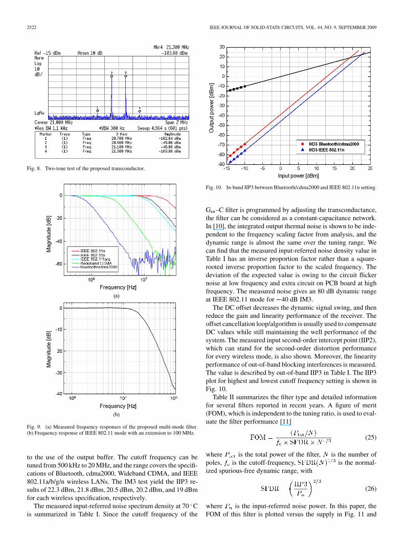
The transconductor has been examined in the frequencydomain to obtain its linearity performance. Fig. 8 shows thespectrum of the transconductor through inter-modulation char-acterization by applying two-tone signals near 20 MHz withthe amplitude of 0.6 voltage. In this measurement, thetransconductance is 100 S and the loading resistor is 50 ohm.The result shows the third-order inter-modulation distortion(IM3) is around 54 dB. The measured performance is smallerthan the expected value from simulation. This is owing tothe deviation of the feedback amplifier gain and the effect ofparasitic capacitance at high frequency.
Fig. 9 illustrates the filter frequency response at 1.2 V supplyvoltage. We should note that the magnitude is normalized owing
2522 IEEE JOURNAL OF SOLID-STATE CIRCUITS, VOL. 44, NO. 9, SEPTEMBER 2009
Fig. 8. Two-tone test of the proposed transconductor.
Fig. 9. (a) Measured frequency responses of the proposed multi-mode filter.(b) Frequency response of IEEE 802.11 mode with an extension to 100 MHz.
to the use of the output buffer. The cutoff frequency can betuned from 500 kHz to 20 MHz, and the range covers the specifi-cations of Bluetooth, cdma2000, Wideband CDMA, and IEEE802.11a/b/g/n wireless LANs. The IM3 test yield the IIP3 re-sults of 22.3 dBm, 21.8 dBm, 20.5 dBm, 20.2 dBm, and 19 dBmfor each wireless specification, respectively.
The measured input-referred noise spectrum density at 70 Cis summarized in Table I. Since the cutoff frequency of the
Fig. 10. In-band IIP3 between Bluetooth/cdma2000 and IEEE 802.11n setting.
G –C filter is programmed by adjusting the transconductance,the filter can be considered as a constant-capacitance network.In [10], the integrated output thermal noise is shown to be inde-pendent to the frequency scaling factor from analysis, and thedynamic range is almost the same over the tuning range. Wecan find that the measured input-referred noise density value inTable I has an inverse proportion factor rather than a square-rooted inverse proportion factor to the scaled frequency. Thedeviation of the expected value is owing to the circuit flickernoise at low frequency and extra circuit on PCB board at highfrequency. The measured noise gives an 80 dB dynamic rangeat IEEE 802.11 mode for 40 dB IM3.
The DC offset decreases the dynamic signal swing, and thenreduce the gain and linearity performance of the receiver. Theoffset cancellation loop/algorithm is usually used to compensateDC values while still maintaining the well performance of thesystem. The measured input second-order intercept point (IIP2),which can stand for the second-order distortion performancefor every wireless mode, is also shown. Moreover, the linearityperformance of out-of-band blocking interferences is measured.The value is described by out-of-band IIP3 in Table I. The IIP3plot for highest and lowest cutoff frequency setting is shown inFig. 10.
Table II summarizes the filter type and detailed informationfor several filters reported in recent years. A figure of merit(FOM), which is independent to the tuning ratio, is used to eval-uate the filter performance [11]
(25)
where is the total power of the filter, is the number ofpoles, is the cutoff-frequency, is the normal-ized spurious-free dynamic range, with
(26)
where is the input-referred noise power. In this paper, theFOM of this filter is plotted versus the supply in Fig. 11 and

LO et al.: A WIDE TUNING RANGE G –C FILTER FOR MULTI-MODE CMOS DIRECT-CONVERSION WIRELESS RECEIVERS 2523
TABLE IPERFORMANCE SUMMARY OF THIS WORK
TABLE IICOMPARISON WITH PREVIOUSLY REPORTED WORKS
Fig. 11. FOM versus supply comparison with previously published works.
favorably compared to other published works, where someof them are not G –C prototypes. In this figure, symbols L
and H denote the lowest and highest frequency for each filter,respectively.
V. CONCLUSION
The CMOS implementation of a third-order Butterworth low-pass G –C filter for multi-mode applications is presented. Thetransconductor is designed by the combination of a voltage-to-current circuit and a current multiplier to achieve both the highlinearity and wide tuning range simultaneously. Through theuse of the wide tuning range linear transconductor as a buildingblock, the cutoff frequency of the channel selection filter can bewidely tuned from 500 kHz to 20 MHz, which meets the speci-fications of Bluetooth, cdma2000, Wideband CDMA, and IEEE802.11a/b/g/n wireless LANs under direct-conversion architec-ture. The theoretical analysis of the operation and the measure-ment results are provided to demonstrate the validity of the filter.
ACKNOWLEDGMENT
The authors would like to thank the National Chip Implemen-tation Center of Taiwan for supporting the chip fabrication.

2524 IEEE JOURNAL OF SOLID-STATE CIRCUITS, VOL. 44, NO. 9, SEPTEMBER 2009
REFERENCES
[1] M. Ismail and T. Fiez, Analog VLSI Signal and Information Pro-cessing. New York: McGraw-Hill, 1994.
[2] S. R. Zarabadi, M. Ismail, and C.-C. Hung, “High performance analogVLSI computational circuits,” IEEE J. Solid-State Circuits, vol. 33, pp.644–649, Apr. 1998.
[3] T. Y. Lo and C. C. Hung, “A 1-V 50 MHz pseudo-differential OTA withcompensation of the mobility reduction,” IEEE Trans. Circuits Syst. II,Expr. Briefs, vol. 54, no. 12, pp. 1047–1051, Dec. 2007.
[4] T. Y. Lo and C. C. Hung, “A 40-MHz double differential-pair CMOSOTA with�60-dB IM3,” IEEE Trans. Circuits Syst. I, Reg. Papers, vol.55, no. 1, pp. 258–265, Feb. 2008.
[5] C. C. Hung, K. A. Halonen, M. Ismail, V. Porra, and A. Hyogo, “A low-voltage, low-power CMOS fifth-order elliptic G –C filter for basebandmobile, wireless communication,” IEEE Trans. Circuits Syst. VideoTechnol., vol. 7, pp. 584–593, Aug. 1997.
[6] B. Fotouhi, “All-MOS voltage-to-current convereter,” IEEE J. Solid-State Circuits, vol. 36, no. 1, pp. 147–151, Jan. 2001.
[7] Y. Tsividis, K. Suyama, and K. Vavelidis, “Simple “reconciliation”MOSFET model valid in all regions,” Electron. Lett., vol. 31, pp.506–508, Mar. 1995.
[8] The BSIM Model. BSIM Research Group, Univ. California, Berkeley[Online]. Available: http://www-device.eecs.berkeley.edu/~bsim3/bsim4.html
[9] U. Yodprasit and C. C. Enz, “A 1.5-V 75-dB dyamic range third-orderG –C filter integrated in a 0.18-�m standard digital CMOS process,”IEEE J. Solid-State Circuits, vol. 38, no. 7, pp. 1189–1197, Jul. 2003.
[10] S. Pavan and Y. Tsividis, “Time-scaled electrical networks. Propertiesand applications in the design of programmable analog filters,” IEEETrans. Circuits Syst. II, vol. 47, pp. 161–165, Feb. 2000.
[11] V. Giannini, J. Craninckx, S. D’Amico, and A. Baschirotto, “Flexiblebaseband analog circuits for software-defined radio front-ends,” IEEEJ. Solid-State Circuits, vol. 42, no. 7, pp. 1501–1512, Jul. 2007.
[12] A. Cathelin, L. Fabre, L. Baud, and D. Belot, “A multiple-shapechannel selection filter for multimode zero-IF receiver using capacitorover active device implementation,” in Proc. ESSCIRC, 2002, pp.651–654.
[13] S. Hori, T. Maeda, H. Yano, N. Matsuno, K. Numata, N. Yoshida, Y.Takahashi, T. Yamase, R. Walkington, and H. Hida, “A widely tun-able CMOS G –C filter with a negative source degeneration resistortransconductor,” in Proc. ESSCIRC, 2003, pp. 449–452.
[14] S. Hori, T. Maeda, N. Matsuno, and H. Hida, “Low-power widelytunable G –C filter with an adaptive Dc-blocking, triode-biasedMOSFET transconductor,” in Proc. ESSCIRC, 2004, pp. 99–102.
[15] D. Chamla, A. Kaiser, A. Cathelin, and D. Belot, “A G –C low-passfilter for zero-IF mobile applications with a very wide tuning range,”IEEE J. Solid-State Circuits, vol. 40, no. 7, pp. 1143–1450, Jul. 2005.
[16] S. D’Amico, V. Giannini, and A. Baschirotto, “A 4th-orderactive-Gm-RC reconfigurable (UMTS/WLAN) filter,” IEEE J.Solid-State Circuits, vol. 40, no. 7, pp. 1143–1450, Jul. 2006.
Tien-Yu Lo received the B.S., M.S., and Ph.D. de-grees in communication engineering from NationalChiao Tung University, Hsinchu, Taiwan, in 2001,2003 and 2007, respectively.
Since 2008, he has been with the Analog CircuitDesign Division, MediaTek Inc., Hsinchu, Taiwan, asan Analog IC Designer. His research interests includeanalog and mixed-signal circuit design with partic-ular focus on the topic of continuous-time filters andanalog-to-digital converters.
Chung-Chih Hung (M’98–SM’07) received theB.S. degree in electrical engineering from NationalTaiwan University, Taipei, Taiwan, in 1989, and theM.S. and Ph.D. degrees in electrical engineeringfrom The Ohio State University, Columbus, in 1993and 1997, respectively.
From 1989 to 1991, he served in the TaiwanMarine Corps as a Communication officer. From1997 to 2003, he worked for several IC designcompanies in San Jose, CA, and San Diego, CA,where he held Analog Circuit Design Manager
and Director positions. Since 2003, he has been with National Chiao TungUniversity, Hsinchu, Taiwan, where he is currently an Associate Professor inthe Department of Electrical Engineering. His research interests include thedesign of analog and mixed-signal integrated circuits for communication andhigh-speed applications.
Mohammed Ismail (F’97) received the B.S. andM.S. degrees in electronics and communicationsfrom Cairo University, Cairo, Egypt, and the Ph.D.degree in electrical engineering from the Universityof Manitoba, Canada.
He has over 25 years experience of R&D in thefields of analog, RF and mixed-signal integrated cir-cuits. He has held several positions in both industryand academia and has served as a corporate consul-tant to nearly 30 companies in the US, Europe, andthe Far East. He is Professor of electrical and com-
puter engineering and the Founding Director of the Analog VLSI Lab at TheOhio State University, Columbus, and of the RaMSiS Group at KTH–Royal In-stitute of Technology, Stockholm, Sweden. His current interest lies in researchinvolving digitally programmable/configurable integrated CMOS radios withfocus on low voltage/low power “first-pass” solutions for cognitive radios, 3 Gand 4 G wireless handhelds. He publishes intensively in this area and has beenawarded 11 patents. He has co-edited and coauthored several books, includingAnalog VLSI Signal and Information Processing (McGraw Hill). His most re-cent book is Radio Design in Nanometer Technologies, (Springer, 2007). Headvised the thesis work of 45 Ph.D. students and of over 85 M.S. students. Heco-founded ANACAD-Egypt (now part of Mentor Graphics, Inc.) and FirstpassTechnologies Inc., a developer of CMOS radio and mixed-signal IPs for hand-held wireless applications.
Dr. Ismail has been the recipient of several awards, including the US NationalScience Foundation Presidential Young Investigator Award, the US Semicon-ductor Research Corp Inventor Recognition Awards in 1992 and 1993, The Col-lege of Engineering Lumley Research Award in 1992,1997, 2002 and 2007 anda Fulbright/Nokia fellowship Award in 1995. He is the founder of the Interna-tional Journal of Analog Integrated Circuits and Signal Processing (Springer)and serves as the Journal’s Editor-In-Chief. He has served as Associate Editorfor many IEEE transactions, is on the International Advisory Boards of severaljournals, and was on the Board of Governors of the IEEE Circuits and SystemsSociety. He is the founder of ICECS, the CAS flagship Conference for Region 8.