LM34917A Ultra Small 33V, 1.25A Constant On-Time Buck ...
22
FB SW LM34917A BST VCC ISEN RON/SD VIN C1 SHUT DOWN SS RTN R ON C6 8V - 33V Input C3 C4 L1 D1 R1 R3 R2 C2 V OUT C7 C8 SGND LM34917A www.ti.com SNOSAX7D – DECEMBER 2007 – REVISED MARCH 2013 LM34917A Ultra Small 33V, 1.25A Constant On-Time Buck Switching Regulator with Intelligent Current Limit Check for Samples: LM34917A 1FEATURES PACKAGE 2• Functional Input Voltage Range: 8V to 33V • 12-Bump DSBGA Package • DSBGA package DESCRIPTION • Input Over-Voltage Shutdown at ≊35V The LM34917A Step-Down Switching Regulator • Transient Capability to 50V features all the functions needed to implement a low • Integrated N-Channel buck switch cost, efficient, buck bias regulator capable of supplying at least 1.25A to the load. To reduce • Valley current limit varies with V IN and V OUT to excessive switch current due to the possibility of a reduce excessive inductor current saturating inductor the valley current limit threshold • On-time is reduced when in current limit changes with input and output voltages, and the on- • Integrated start-up regulator time is reduced when current limit is detected. This buck regulator contains an N-Channel Buck Switch, • No loop compensation required and is available in the 12 pin DSBGA package. The • Ultra-Fast transient response constant on-time feedback regulation scheme • Maximum switching frequency: 2 MHz requires no loop compensation, results in fast load transient response, and simplifies circuit • Operating frequency remains nearly constant implementation. The operating frequency remains with load current and input voltage variations constant with line and load variations due to the • Programmable soft-start inverse relationship between the input voltage and • Precision internal reference the on-time. The valley current limit results in a smooth transition from constant voltage to constant • Adjustable output voltage current mode when current limit is detected, reducing • Thermal shutdown the frequency and output voltage, without the use of foldback. Additional features include: V CC under- TYPICAL APPLICATIONS voltage lock-out, input over-voltage shutdown, thermal shutdown, gate drive under-voltage lock-out, • High Efficiency Point-Of-Load (POL) Regulator and maximum duty cycle limit. • Non-Isolated Buck Regulator • Secondary High Voltage Post Regulator Basic Step Down Regulator 1 Please be aware that an important notice concerning availability, standard warranty, and use in critical applications of Texas Instruments semiconductor products and disclaimers thereto appears at the end of this data sheet. 2All trademarks are the property of their respective owners. PRODUCTION DATA information is current as of publication date. Copyright © 2007–2013, Texas Instruments Incorporated Products conform to specifications per the terms of the Texas Instruments standard warranty. Production processing does not necessarily include testing of all parameters.
-
Upload
khangminh22 -
Category
Documents
-
view
1 -
download
0
Transcript of LM34917A Ultra Small 33V, 1.25A Constant On-Time Buck ...

FB
SW
LM34917A
BST
VCC
ISEN
RON/SD
VIN
C1
SHUTDOWN
SS
RTN
RON
C6
8V - 33VInput
C3
C4
L1
D1R1
R3
R2
C2
VOUT
C7
C8
SGND
LM34917A
www.ti.com SNOSAX7D –DECEMBER 2007–REVISED MARCH 2013
LM34917A Ultra Small 33V, 1.25A Constant On-Time Buck Switching Regulator withIntelligent Current Limit
Check for Samples: LM34917A
1FEATURES PACKAGE2• Functional Input Voltage Range: 8V to 33V • 12-Bump DSBGA Package• DSBGA package
DESCRIPTION• Input Over-Voltage Shutdown at ≊≊35VThe LM34917A Step-Down Switching Regulator• Transient Capability to 50V features all the functions needed to implement a low
• Integrated N-Channel buck switch cost, efficient, buck bias regulator capable ofsupplying at least 1.25A to the load. To reduce• Valley current limit varies with VIN and VOUT toexcessive switch current due to the possibility of areduce excessive inductor currentsaturating inductor the valley current limit threshold
• On-time is reduced when in current limit changes with input and output voltages, and the on-• Integrated start-up regulator time is reduced when current limit is detected. This
buck regulator contains an N-Channel Buck Switch,• No loop compensation requiredand is available in the 12 pin DSBGA package. The• Ultra-Fast transient responseconstant on-time feedback regulation scheme
• Maximum switching frequency: 2 MHz requires no loop compensation, results in fast loadtransient response, and simplifies circuit• Operating frequency remains nearly constantimplementation. The operating frequency remainswith load current and input voltage variationsconstant with line and load variations due to the• Programmable soft-start inverse relationship between the input voltage and
• Precision internal reference the on-time. The valley current limit results in asmooth transition from constant voltage to constant• Adjustable output voltagecurrent mode when current limit is detected, reducing• Thermal shutdownthe frequency and output voltage, without the use offoldback. Additional features include: VCC under-TYPICAL APPLICATIONS voltage lock-out, input over-voltage shutdown,thermal shutdown, gate drive under-voltage lock-out,• High Efficiency Point-Of-Load (POL) Regulatorand maximum duty cycle limit.• Non-Isolated Buck Regulator
• Secondary High Voltage Post Regulator
Basic Step Down Regulator
1
Please be aware that an important notice concerning availability, standard warranty, and use in critical applications ofTexas Instruments semiconductor products and disclaimers thereto appears at the end of this data sheet.
2All trademarks are the property of their respective owners.
PRODUCTION DATA information is current as of publication date. Copyright © 2007–2013, Texas Instruments IncorporatedProducts conform to specifications per the terms of the TexasInstruments standard warranty. Production processing does notnecessarily include testing of all parameters.

D3D2D1
C3C2C1
B3B2B1
A3A2A1
SW
VIN
RON
RTN
BST
VCC
SS
FB
SW
VIN
ISEN
SGND
D1D2D3
C1C2C3
B1B2B3
A1A2A3
LM34917A
SNOSAX7D –DECEMBER 2007–REVISED MARCH 2013 www.ti.com
Connection Diagram
Figure 1. Bump Side Figure 2. Top ViewPackage Number YZR0012UNA Package Number YZR0012UNA
PIN DESCRIPTIONSPin Number Name Description Application Information
A1 SGND Sense Ground Re-circulating current flows into this pin to the current senseresistor.
A2 RTN Circuit Ground Ground for all internal circuitry other than the current limitdetection.
A3 FB Feedback input from the regulated Internally connected to the regulation and over-voltageoutput comparators. The regulation level is 2.5V.
B1 ISEN Current sense The re-circulating current flows out of this pin to the free-wheeling diode.
B2 RON/SD On-time control and shutdown An external resistor from VIN to this pin sets the buck switchon-time. Grounding this pin shuts down the regulator.
B3 SS Softstart An internal current source charges an external capacitor to2.5V, providing the softstart function.
C1,C2 VIN Input supply voltage Operating input range is 8.0V to 33V, with over-voltageshutdown internally set at ≊35V. Transient capability is 50V.
C3 VCC Output from the startup regulator Nominally regulated at 7.0V. Connect a 0.1 µF capacitor fromthis pin to RTN. An external voltage (8V to 14V) can beapplied to this pin to reduce internal dissipation. An internaldiode connects VCC to VIN.
D1,D2 SW Switching Node Internally connected to the buck switch source. Connect tothe inductor, diode, and bootstrap capacitor.
D3 BST Boost pin for bootstrap capacitor Connect a 0.022 µF capacitor from SW to this pin. Thecapacitor is charged each off-time via an internal diode.
These devices have limited built-in ESD protection. The leads should be shorted together or the device placed in conductive foamduring storage or handling to prevent electrostatic damage to the MOS gates.
2 Submit Documentation Feedback Copyright © 2007–2013, Texas Instruments Incorporated
Product Folder Links: LM34917A

LM34917A
www.ti.com SNOSAX7D –DECEMBER 2007–REVISED MARCH 2013
Absolute Maximum Ratings (1) (2)
VIN to RTN 50V
BST to RTN 64V
SW to RTN (Steady State) -1.5V
BST to VCC 50V
VIN to SW 50V
BST to SW 14V
VCC to RTN 14V
SGND to RTN -0.3V to +0.3V
Current out of ISEN See text
SS to RTN -0.3V to 4V
All Other Inputs to RTN -0.3 to 7V
ESD Rating (3)
Human Body Model 2kV
Storage Temperature Range -65°C to +150°C
Junction Temperature 150°C
(1) Absolute Maximum Ratings are limits beyond which damage to the device may occur. Operating Ratings are conditions under whichoperation of the device is intended to be functional. For specifications and test conditions, see the Electrical Characteristics.
(2) If Military/Aerospace specified devices are required, please contact the TI Sales Office/Distributors for availability and specifications.(3) The human body model is a 100pF capacitor discharged through a 1.5kΩ resistor into each pin.
Operating Ratings (1)
VIN Voltage 8.0V to 33V
Junction Temperature −40°C to + 125°C
(1) Absolute Maximum Ratings are limits beyond which damage to the device may occur. Operating Ratings are conditions under whichoperation of the device is intended to be functional. For specifications and test conditions, see the Electrical Characteristics.
Electrical CharacteristicsLimits in standard type are for TJ = 25°C only; limits in boldface type apply over the junction temperature (TJ) range of -40°Cto +125°C. Minimum and Maximum limits are specified through test, design, or statistical correlation. Typical values representthe most likely parametric norm at TJ = 25°C, and are provided for reference purposes only. Unless otherwise stated thefollowing conditions apply: VIN = 12V, RON = 200kΩ. See (1) and (2).
Symbol Parameter Conditions Min Typ Max Units
Start-Up Regulator, VCC
VCCReg VCC regulated output Vin > 9V 6.6 7.0 7.4 V
VIN-VCC dropout voltage ICC = 0 mA, 1.3 VVCC = UVLOVCC + 250 mV
VCC output impedance VIN = 8V 150 Ω(0 mA ≤ ICC ≤ 5 mA) VIN = 12V 0.75
VCC current limit (3) VCC = 0V 11 mA
UVLOVCC VCC under-voltage lockout VCC increasing 5.45 Vthreshold
UVLOVCC hysteresis VCC decreasing 145 mV
UVLOVCC filter delay 100 mV overdrive 3 µs
IIN operating current Non-switching, FB = 3V 0.68 0.95 mA
IIN shutdown current RON/SD = 0V 85 160 µA
Switch Characteristics
Rds(on) Buck Switch Rds(on) ITEST = 200 mA 0.33 0.7 ΩUVLOGD Gate Drive UVLO VBST - VSW Increasing 2.65 4 4.62 V
(1) For detailed information on soldering DSBGA packages, refer to Application Note AN-1112 (SNVA009).(2) Typical specifications represent the most likely parametric norm at 25°C operation.(3) VCC provides self bias for the internal gate drive and control circuits. Device thermal limitations limit external loading
Copyright © 2007–2013, Texas Instruments Incorporated Submit Documentation Feedback 3
Product Folder Links: LM34917A

LM34917A
SNOSAX7D –DECEMBER 2007–REVISED MARCH 2013 www.ti.com
Electrical Characteristics (continued)Limits in standard type are for TJ = 25°C only; limits in boldface type apply over the junction temperature (TJ) range of -40°Cto +125°C. Minimum and Maximum limits are specified through test, design, or statistical correlation. Typical values representthe most likely parametric norm at TJ = 25°C, and are provided for reference purposes only. Unless otherwise stated thefollowing conditions apply: VIN = 12V, RON = 200kΩ. See (1) and (2).
Symbol Parameter Conditions Min Typ Max Units
UVLOGD hysteresis 450 mV
Softstart Pin
VSS Pull-up voltage 2.5 V
ISS Internal current source 11.6 µA
VRES Restart threshold after OVP 0.18 Vshutdown
Current Limit
ILIM Threshold VIN = 8V, VFB = 2.4V 1.15 1.35 1.55 A
VIN = 30V, VFB = 2.4V 1.05 1.2 1.45
VIN = 30V, VFB = 1.0V 0.95 1.15 1.35
Response time 150 ns
On Timer
tON - 1 On-time (normal operation) VIN = 10V, RON = 200 kΩ 2.1 2.8 3.5 µs
tON - 2 On-time (normal operation) VIN = 32V, RON = 200 kΩ 860 ns
tON - 3 On-time (current limit) VIN = 10V, RON = 200 kΩ 1.13 µs
Shutdown threshold at RON/SD Voltage at RON/SD rising 0.3 0.65 1.0 V
Shutdown Threshold hysteresis Voltage at RON/SD falling 40 mV
Off Timer
tOFF Minimum Off-time 90 ns
Regulation and Over-Voltage Comparators (FB Pin)
VREF FB regulation threshold SS pin = steady state 2.445 2.50 2.550 V
FB over-voltage threshold 2.9 V
FB bias current FB = 3V 10 nA
Input Over-Voltage Shutdown
VIN(OV) Shutdown voltage threshold at VIN increasing 33.0 34.8 36.9 VVIN
Thermal Shutdown
TSD Thermal shutdown temperature Junction temperature rising 175 °C
Thermal shutdown hysteresis 20 °C
Thermal Resistance
θJA Junction to Ambient 58 °C/W0 LFPM Air Flow
4 Submit Documentation Feedback Copyright © 2007–2013, Texas Instruments Incorporated
Product Folder Links: LM34917A

0 0.5 1.0 1.5 2.0 2.51.0
1.1
1.2
1.3
1.4
1.5
VA
LLE
Y C
UR
RE
NT
LIM
IT T
HR
ES
HO
LD (
A)
VFB (V)
VIN = 8V
15V
24V
33V
5 10 15 20 25 30 35
VIN (V)
0
1.0
2.0
3.0
RO
N/S
D P
IN V
OLT
AG
E (
V)
100k
600k
RON = 50k
200k
6.5 7.0 7.5 8.0 8.5 9.05.0
5.5
6.0
6.5
7.0
7.5
VC
C (
V)
VIN (V)
FS = 350 kHz
FS = 94 kHz
FS = 700 kHz
100 k:
5 35
VIN (V)
10 15 20 25 30
0.1
1.0
10
ON
-TIM
E (P
s)
0.3
3.0
50 k:
400 k:
200 k:
RON = 600 k:
LM34917A
www.ti.com SNOSAX7D –DECEMBER 2007–REVISED MARCH 2013
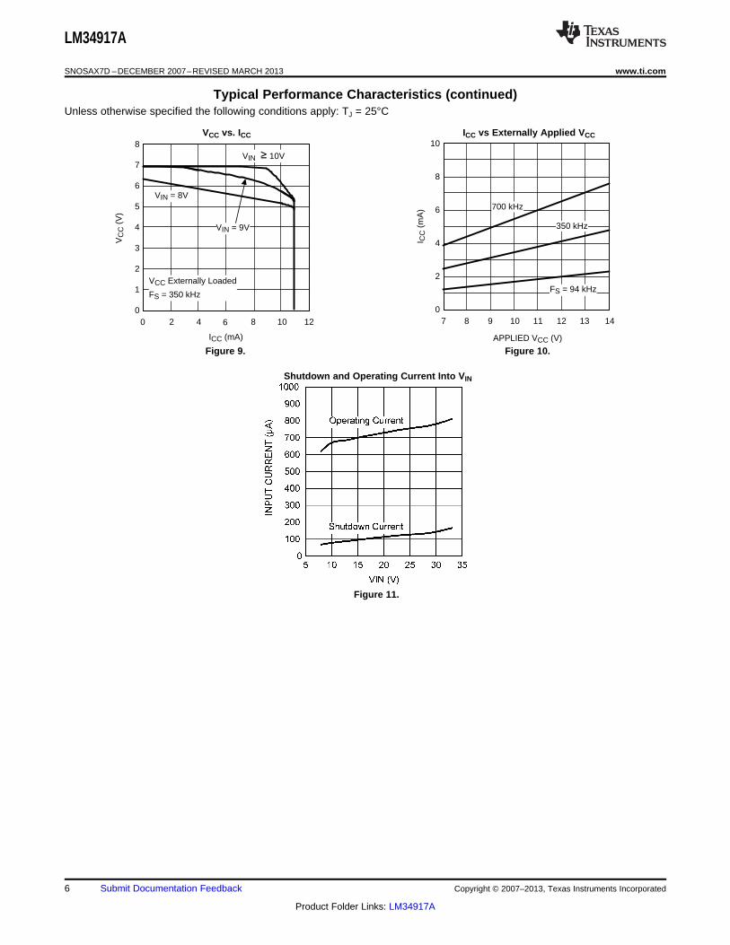
Typical Performance CharacteristicsUnless otherwise specified the following conditions apply: TJ = 25°C
Efficiency at 1.5 MHz Efficiency at 2 MHz
Figure 3. Figure 4.
VCC vs. VIN ON-Time vs. VIN and RON
Figure 5. Figure 6.
Valley Current Limit Threshold vs. VFB and VIN Voltage at the RON/SD Pin
Figure 7. Figure 8.
Copyright © 2007–2013, Texas Instruments Incorporated Submit Documentation Feedback 5
Product Folder Links: LM34917A
7 8 9 10 11 12 13 140
2
4
6
8
10
I CC
(m
A)
APPLIED VCC (V)
FS = 94 kHz
350 kHz
700 kHz
0 2 4 6 8 10 12
ICC (mA)
0
1
2
3
4
5
6
7
8
VC
C (
V)
VIN = 9V
VIN = 8V
VCC Externally Loaded
FS = 350 kHz
VIN 8 10V
LM34917A
SNOSAX7D –DECEMBER 2007–REVISED MARCH 2013 www.ti.com
Typical Performance Characteristics (continued)Unless otherwise specified the following conditions apply: TJ = 25°C
VCC vs. ICC ICC vs Externally Applied VCC
Figure 9. Figure 10.
Shutdown and Operating Current Into VIN
Figure 11.
6 Submit Documentation Feedback Copyright © 2007–2013, Texas Instruments Incorporated
Product Folder Links: LM34917A

FB SW
RTN
BST
SS
C3
LM34917A
SD
+-
SGND
ISEN
Input
GND
RON/SD
+-
ON TIMER
LOGIC
FINISHSTART
Driver
FB
8V - 33V
2.5V
2.9V
0.65V
C4
D1
R1
R2
C2
C5
C1
C6
RON
CURRENT LIMITCOMPARATOR
OVER-VOLTAGECOMPARATOR
REGULATIONCOMPARATOR
VIN VCC
VOUT
VIN
VIN
RSENSE
11.6 PA
41 m:
RON
7V START-UPREGULATOR
LEVELSHIFT
Gate DriveUVLO
VCC
UVLO
CLThreshold
Adjust
MINIMUMOFF TIMERSTART
FINISH' Ton
+
34.8V
0V SHUTDOWN
THERMALSHUTDOWN
L1
R3 C8
C7
LM34917A
www.ti.com SNOSAX7D –DECEMBER 2007–REVISED MARCH 2013
Typical Application Circuit and Block Diagram
Copyright © 2007–2013, Texas Instruments Incorporated Submit Documentation Feedback 7
Product Folder Links: LM34917A
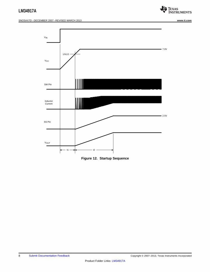
UVLO
VIN
VCC
SW Pin
InductorCurrent
SS Pin
t2
VOUT
7.0V
2.5V
t1
LM34917A
SNOSAX7D –DECEMBER 2007–REVISED MARCH 2013 www.ti.com
Figure 12. Startup Sequence
8 Submit Documentation Feedback Copyright © 2007–2013, Texas Instruments Incorporated
Product Folder Links: LM34917A

fSW =VOUT
2 x L1 x 1.48 x 1020
RL x RON2
DC =tON
tON + tOFF
VOUT
VIN = tON x fSW =
fSW =VOUT x (VIN ± 1.35V)
VIN x 1.16 x 10⁻¹⁰ x (RON + 1.4k)
LM34917A
www.ti.com SNOSAX7D –DECEMBER 2007–REVISED MARCH 2013
FUNCTIONAL DESCRIPTION
The LM34917A Step Down Switching Regulator features all the functions needed to implement a low cost,efficient buck bias power converter capable of supplying at least 1.25A to the load. This high voltage regulatorcontains an N-Channel buck switch, is easy to implement, and is available in the DSBGA package. Theregulator’s operation is based on a constant on-time control scheme where the on-time is inversely proportionalto the input voltage. This feature results in the operating frequency remaining relatively constant with load andinput voltage variations. The feedback control scheme requires no loop compensation resulting in very fast loadtransient response. The valley current limit scheme protects against excessively high currents if the output isshort circuited when VIN is high. To aid in controlling excessive switch current due to a possible saturatinginductor the valley current limit threshold changes with input and output voltages, and the on-time is reduced byapproximately 50% when current limit is detected. An over-voltage detection at VIN stops the circuit's switchingwhen the input voltage exceeds 34.8V. The LM34917A can be applied in numerous applications to efficientlyregulate down higher voltages. Additional features include: Thermal shutdown, VCC under-voltage lock-out, gatedrive under-voltage lock-out, and maximum duty cycle limit.
Control Circuit Overview
The LM34917A buck DC-DC regulator employs a control scheme based on a comparator and a one-shot on-timer, with the output voltage feedback (FB) compared to an internal reference (2.5V). If the FB voltage is belowthe reference the buck switch is switched on for a time period determined by the input voltage and aprogramming resistor (RON). Following the on-time the switch remains off until the FB voltage falls below thereference, but for a time not less than the minimum off-time forced by the LM34917A. The buck switch is thenswitched on for another on-time period.
When in regulation, the LM34917A operates in continuous conduction mode at heavy load currents anddiscontinuous conduction mode at light load currents. In continuous conduction mode the inductor’s current isalways greater than zero, and the operating frequency remains relatively constant with load and line variations.The minimum load current for continuous conduction mode is one-half the inductor’s ripple current amplitude.The approximate operating frequency is calculated as follows:
(1)
The buck switch duty cycle is equal to:
(2)
In discontinuous conduction mode, where the inductor’s current reaches zero during the off-time forcing a longer-than-normal off-time, the operating frequency is lower than in continuous conduction mode, and varies with loadcurrent. Conversion efficiency is maintained at light loads since the switching losses reduce with the reduction inload and frequency. The approximate discontinuous operating frequency can be calculated as follows:
(3)
where RL = the load resistance, and L1 is the circuit’s inductor.
The output voltage is set by the two feedback resistors (R1, R2 in the Block Diagram). The regulated outputvoltage is calculated as follows:
VOUT = 2.5 x (R1 + R2) / R2 (4)
Output voltage regulation is based on supplying ripple voltage to the feedback input (FB pin) in phase with theSW pin. The LM34917A requires a minimum of 25 mVp-p of ripple voltage at the FB pin. The ripple is generatedas a triangle wavefrom at the junction of R3 and C8 as the SW pin switches high and low, and fed to the FB pinby C7.
If the voltage at FB rises above 2.9V, due to a transient at VOUT or excessive inductor current which createshigher than normal ripple at VOUT, the internal over-voltage comparator immediately shuts off the internal buckswitch. The next on-time starts when the voltage at FB falls below 2.5V and the inductor current falls below thecurrent limits threshold.
Copyright © 2007–2013, Texas Instruments Incorporated Submit Documentation Feedback 9
Product Folder Links: LM34917A
STOP
RUN
RON/SD
InputVoltage
LM34917A
VIN
RON
RON =VOUT x (VIN - 1.35V)
VIN x 1.16 x 10⁻¹⁰ x fSW
-1.4k:
tON =VIN - 1.35V
1.16 x 10⁻¹⁰ x (RON + 1.4 k:)+ 100 ns
LM34917A
SNOSAX7D –DECEMBER 2007–REVISED MARCH 2013 www.ti.com
ON-Time Timer
The on-time for the LM34917A is determined by the RON resistor and the input voltage (VIN), calculated from:
(5)
The inverse relationship with VIN results in a nearly constant frequency as VIN is varied. To set a specificcontinuous conduction mode switching frequency (fSW), the RON resistor is determined from the following:
(6)
Equation 1, Equation 5 and Equation 6 are valid only during normal operation - i.e., the circuit is not in currentlimit. When the LM34917A operates in current limit, the on-time is reduced by approximately 50%. This featurereduces the peak inductor current which may be excessively high if the load current and the input voltage aresimultaneously high. This feature operates on a cycle-by-cycle basis until the load current is reduced and theoutput voltage resumes its normal regulated value. Equation 1, Equation 5 and Equation 6 have a ±25%tolerance.
Remote Shutdown
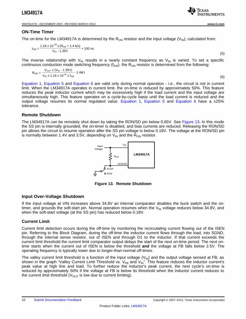
The LM34917A can be remotely shut down by taking the RON/SD pin below 0.65V. See Figure 13. In this modethe SS pin is internally grounded, the on-timer is disabled, and bias currents are reduced. Releasing the RON/SDpin allows the circuit to resume operation after the SS pin voltage is below 0.18V. The voltage at the RON/SD pinis normally between 1.4V and 3.5V, depending on VIN and the RON resistor.
Figure 13. Remote Shutdown
Input Over-Voltage Shutdown
If the input voltage at VIN increases above 34.8V an internal comparator disables the buck switch and the on-timer, and grounds the soft-start pin. Normal operation resumes when the VIN voltage reduces below 34.8V, andwhen the soft-start voltage (at the SS pin) has reduced below 0.18V.
Current Limit
Current limit detection occurs during the off-time by monitoring the recirculating current flowing out of the ISENpin. Referring to the Block Diagram, during the off-time the inductor current flows through the load, into SGND,through the internal sense resistor, out of ISEN and through D1 to the inductor. If that current exceeds thecurrent limit threshold the current limit comparator output delays the start of the next on-time period. The next on-time starts when the current out of ISEN is below the threshold and the voltage at FB falls below 2.5V. Theoperating frequency is typically lower due to longer-than-normal off-times.
The valley current limit threshold is a function of the input voltage (VIN) and the output voltage sensed at FB, asshown in the graph “Valley Current Limit Threshold vs. VFB and VIN”. This feature reduces the inductor current’speak value at high line and load. To further reduce the inductor’s peak current, the next cycle’s on-time isreduced by approximately 50% if the voltage at FB is below its threshold when the inductor current reduces tothe current limit threshold (VOUT is low due to current limiting).
10 Submit Documentation Feedback Copyright © 2007–2013, Texas Instruments Incorporated
Product Folder Links: LM34917A
'I
IOUT2
IOUT3
NormalOperation
Load CurrentDecreases
CurrentLimited
LoadCurrent
Increases
NormalOperation
Current LimitThreshold
Ind
uct
or
Cu
rren
tF
eed
bac
kV
olt
age
@ F
B P
in
IOUT1
TON
2.5V
TON
2
LM34917A
www.ti.com SNOSAX7D –DECEMBER 2007–REVISED MARCH 2013
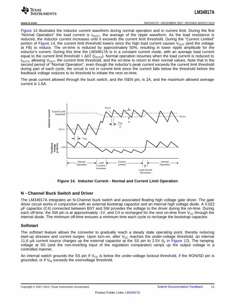
Figure 14 illustrates the inductor current waveform during normal operation and in current limit. During the first“Normal Operation” the load current is IOUT1, the average of the ripple waveform. As the load resistance isreduced, the inductor current increases until it exceeds the current limit threshold. During the “Current Limited”portion of Figure 14, the current limit threshold lowers since the high load current causes VOUT (and the voltageat FB) to reduce. The on-time is reduced by approximately 50%, resulting in lower ripple amplitude for theinductor’s current. During this time the LM34917A is in a constant current mode, with an average load currentequal to the current limit threshold + ΔI/2 (IOUT2). Normal operation resumes when the load current is reduced toIOUT3, allowing VOUT, the current limit threshold, and the on-time to return to their normal values. Note that in thesecond period of “Normal Operation”, even though the inductor’s peak current exceeds the current limit thresholdduring part of each cycle, the circuit is not in current limit since the current falls below the threshold before thefeedback voltage reduces to its threshold to initiate the next on-time.
The peak current allowed through the buck switch, and the ISEN pin, is 2A, and the maximum allowed averagecurrent is 1.5A.
Figure 14. Inductor Current - Normal and Current Limit Operation
N - Channel Buck Switch and Driver
The LM34917A integrates an N-Channel buck switch and associated floating high voltage gate driver. The gatedriver circuit works in conjunction with an external bootstrap capacitor and an internal high voltage diode. A 0.022µF capacitor (C4) connected between BST and SW provides the voltage to the driver during the on-time. Duringeach off-time, the SW pin is at approximately -1V, and C4 is recharged for the next on-time from VCC through theinternal diode. The minimum off-time ensures a minimum time each cycle to recharge the bootstrap capacitor.
Softstart
The softstart feature allows the converter to gradually reach a steady state operating point, thereby reducingstart-up stresses and current surges. Upon turn-on, after VCC reaches the under-voltage threshold, an internal11.6 µA current source charges up the external capacitor at the SS pin to 2.5V (t2 in Figure 12). The rampingvoltage at SS (and the non-inverting input of the regulation comparator) ramps up the output voltage in acontrolled manner.
An internal switch grounds the SS pin if VCC is below the under-voltage lockout threshold, if the RON/SD pin isgrounded, or if VIN exceeds the overvoltage threshold.
Copyright © 2007–2013, Texas Instruments Incorporated Submit Documentation Feedback 11
Product Folder Links: LM34917A

L1(min) =ton(min) x (VIN(max) ± VOUT)
IOR(max)= 13.2 PH
RON =VOUT x (VIN(min) - 1.35V)
VIN(min) x 1.16 x 10⁻¹⁰ x fSW
- 1.4 k:= 22.49 k:
fSW <VIN - VOUT
VIN x 105 ns= 3.57 MHz at VIN = 8V
LM34917A
SNOSAX7D –DECEMBER 2007–REVISED MARCH 2013 www.ti.com
Thermal Shutdown
The LM34917A should be operated so the junction temperature does not exceed 125°C. If the junctiontemperature increases above that, an internal Thermal Shutdown circuit activates (typically) at 175°C, taking thecontroller to a low power reset state by disabling the buck switch. This feature helps prevent catastrophic failuresfrom accidental device overheating. When the junction temperature reduces below 155°C (typical hysteresis =20°C), normal operation resumes.
Applications Information
EXTERNAL COMPONENTS
The procedure for calculating the external components is illustrated with the following design example. Referringto the Block Diagram, the circuit is to be configured for the following specifications:• VOUT = 5V• VIN = 8V to 33V• Minimum load current = 200 mA• Maximum load current = 1000 mA• Switching Frequency = 1.5 MHz• Soft-start time = 5 ms• Output voltage ripple level: Minimum
R1 and R2: These resistors set the output voltage. The ratio of the feedback resistors is calculated from:R1/R2 = (VOUT/2.5V) - 1 (7)
For this example, R1/R2 = 1. R1 and R2 should be chosen from standard value resistors in the range of 1.0 kΩ –10 kΩ which satisfy the above ratio. For this example, 2.49 kΩ is chosen for R1 and R2.
RON: This resistor sets the on-time, and (by default) the switching frequency. Since the maximum frequency islimited by the minimum off-time forced by the LM34917A, first check that the desired frequency is less than:
(8)
The RON resistor is calculated from Equation 6 using the minimum input voltage:
(9)
Equation 5 is used to verify that this value resistor does not set an on-time less than 120 ns at maximum inputvoltage. A standard value 22.1 kΩ resistor is used, resulting in a nominal frequency of 1.49 MHz. The minimumon-time is 188 ns at Vin = 33V, and the maximum on-time is 510 ns at Vin = 8V.
L1: The main parameter affected by the inductor is the inductor current ripple amplitude (IOR). The minimum loadcurrent is used to determine the maximum allowable ripple in order to maintain continuous conduction mode,where the lower peak does not reach 0 mA. This is not a requirement of the LM34917A, but serves as aguideline for selecting L1. For this example, the maximum ripple current should be less than:
IOR(MAX) = 2 x IOUT(min) = 400 mAp-p (10)
For other applications, if the minimum load current is zero, use 20% of IOUT(max) for IOUT(min) in Equation 10. Theripple amplitude calculated in Equation 10 is then used in the following equation:
(11)
A standard value 15 µH inductor is selected. The maximum ripple amplitude, which occurs at maximum VIN,calculates to 351 mA p-p, and the peak current is 1175 mA at maximum load current. Ensure the selectedinductor is rated for this peak current.
C2: C2 should typically be no smaller than 3.3 µF, although that is dependent on the frequency and the desiredoutput characteristics. C2 should be a low ESR good quality ceramic capacitor. Experimentation is usuallynecessary to determine the minimum value for C2, as the nature of the load may require a larger value. A loadwhich creates significant transients requires a larger value for C2 than a non-varying load.
12 Submit Documentation Feedback Copyright © 2007–2013, Texas Instruments Incorporated
Product Folder Links: LM34917A

R3 x C8 =(VIN (min) - VA) x tON
'V= 17.5 X 10⁻⁶
C6 =t2 x 11.6 PA
2.5V= 0.023 PF
C1 =IOUT (max) x tON
'V= 1.02 PF
LM34917A
www.ti.com SNOSAX7D –DECEMBER 2007–REVISED MARCH 2013
C1 and C5: C1’s purpose is to supply most of the switch current during the on-time, and limit the voltage rippleat VIN, since it is assumed the voltage source feeding VIN has some amount of source impedance.
At maximum load current, when the buck switch turns on, the current into VIN suddenly increases to the lowerpeak of the inductor’s ripple current, ramps up to the upper peak, then drops to zero at turn-off. The averagecurrent during the on-time is the load current. For a worst case calculation, C1 must supply this average loadcurrent during the maximum on-time, without letting the voltage at VIN drop below ≊7.5V. The minimum value forC1 is calculated from:
(12)
where tON is the maximum on-time, and ΔV is the allowable ripple voltage at VIN (0.5V at VIN = 8V). C5’s purposeis to minimize transients and ringing due to long lead inductance leading the VIN pin. A low ESR 0.1 µF ceramicchip capacitor must be located close to the VIN and RTN pins.
C3: The capacitor at the VCC pin provides noise filtering and stability for the VCC regulator. C3 should be nosmaller than 0.1 µF, and should be a good quality, low ESR ceramic capacitor. C3’s value, and the VCC currentlimit, determine a portion of the turn-on-time (t1 in Figure 12).
C4: The recommended value for C4 is 0.022 µF. A high quality ceramic capacitor with low ESR is recommendedas C4 supplies a surge current to charge the buck switch gate at each turn-on. A low ESR also helps ensure acomplete recharge during each off-time.
C6: The capacitor at the SS pin determines the soft-start time, i.e. the time for the output voltage to reach its finalvalue (t2 in Figure 12). The capacitor value is determined from:
(13)
R3, C7, C8: The ripple amplitude at VOUT is determined by C2’s characteristics and the inductor’s ripple currentamplitude, and typically ranges from 5 mV to 30 mV over the Vin range. Since the LM34917A’s regulationcomparator requires a minimum of 25 mVp-p ripple at the FB pin, these three components are added to generateand provide the necessary ripple to FB in phase with the waveform at SW. R3 and C8 are chosen to generate asawtooth waveform at their junction, and that voltage is AC coupled to the FB pin via C7. To determine thevalues for R3, C7 and C8, the following procedure is used:
Calculate VA = VOUT – (VSW x (1 – (VOUT/VIN(min))) (14)
where VSW is the absolute value of the voltage at the SW pin during the off-time (typically 1V). VA, the DCvoltage at the R3/C8 junction, calculates to 4.63V, and is used in the next equation.
(15)
where tON is the maximum on-time (at minimum input voltage), and ΔV is the desired ripple amplitude at theR3/C8 junction, typically 100 mV. R3 and C8 are chosen from standard value components to satisfy the aboveproduct. For this example, 3300 pF is chosen for C8, and 5.23 kΩ is chosen for R3. C7 is chosen largecompared to C8, typically 0.1 µF.
D1: A Schottky diode is recommended. Ultra-fast recovery diodes are not recommended as the high speedtransitions at the SW pin may inadvertently affect the IC’s operation through external or internal EMI. The diodemust be rated for the maximum input voltage, the maximum load current, and the peak current which occurswhen the current limit and maximum ripple current are reached simultaneously. The diode’s average powerdissipation is calculated from:
PD1 = VF x IOUT x (1-D) (16)
where VF is the diode’s forward voltage drop, and D is the on-time duty cycle.
FINAL CIRCUIT
The final circuit is shown in Figure 15, and its performance is shown in Figure 16 and Figure 17. Current limitmeasured approximately 1.34A at Vin = 8V, and 1.27A at Vin = 33V. The output ripple amplitude measured 4mVp-p at Vin = 8V, and 14 mVp-p at Vin = 33V.
Copyright © 2007–2013, Texas Instruments Incorporated Submit Documentation Feedback 13
Product Folder Links: LM34917A

R4 =25 mVIOR (min)
FB
SW
LM34917ABST
VCC C3
ISEN
VIN
SHUTDOWN
SS
RTN SGND
C12 PF
8V to 33VInput
RON/SD
VOUT
5V
C220 PF
3300 pF
C8R3
R1
C7
R2
15 PHL1C4
0.022 PF
D1
0.1 PF
0.1 PF
2.49 k:
2.49 k:
C50.1 PF
C60.022 PF
RON
22.1 k:
5.23 k:
LM34917A
SNOSAX7D –DECEMBER 2007–REVISED MARCH 2013 www.ti.com
Figure 15. Example Circuit
Figure 16. Efficiency vs. Load Current and VIN (Circuit of Figure 15)
Figure 17. Frequency vs. VIN (Circuit of Figure 15)
ALTERNATE OUTPUT RIPPLE CONFIGURATIONS
For applications which can accept higher levels of ripple at VOUT, the following configurations are simpler and abit more economical.
a) Alternate #1: In Figure 18, R3, C7 and C8 are removed, and Cff and R4 are installed, resulting in a higherripple level than the circuit of Figure 15. Ripple is created at VOUT by the inductor’s ripple current passing throughR4. That ripple voltage is AC coupled to the FB pin through Cff, allowing the minimum ripple at VOUT to be set at25 mVp-p. The minimum ripple current amplitude (IOR(min)) is calculated by re-arranging Equation 11 using tON(max)and VIN(min). The minimum value for R4 is calculated from:
(17)
14 Submit Documentation Feedback Copyright © 2007–2013, Texas Instruments Incorporated
Product Folder Links: LM34917A

FB
SW
L1
R1LM34917A
R2
R4
C2
VOUT
R4(min) =25 mV x (R1 + R2)
R2 x IOR (min)
FB
SW
L1
LM34917A Cff R1 R4
R2 C2
VOUT
Cff =tON (max)
(R1//R2)
LM34917A
www.ti.com SNOSAX7D –DECEMBER 2007–REVISED MARCH 2013
The next larger standard value resistor should be selected for R4 to allow for tolerances. The minimum value forCff is determined from:
(18)
The next larger standard value capacitor should be used for Cff.
Figure 18. Reduced Ripple Configuration
b) Alternate #2: In Figure 19, R3, C7 and C8 are removed, and R4 is installed, resulting in a higher ripple levelthan the circuits of Figure 15 and Figure 18. Ripple is created at VOUT by the inductor’s ripple current passingthrough R4. That ripple voltage is coupled to the FB pin through the feedback resistors (R1, R2). Since theLM34917A requires a minimum of 25 mVp-p ripple at the FB pin, the ripple required at VOUT is higher than 25mVp-p by the gain of the feedback resistors. The minimum ripple current (IOR(min)) is calculated by re-arrangingEquation 11 using tON(max) and VIN(min). The minimum value for R4 is calculated from:
(19)
The next larger standard value resistor should be used for R4.
Figure 19. Maximum Ripple Configuration
c) Alternate minimum ripple configuration: The circuit in Figure 20 is the same as that in Figure 19, exceptthe output voltage is taken from the junction of R4 and C2. The ripple at VOUT is determined by the inductor’sripple current and C2’s characteristics. However, R4 slightly degrades the load regulation. This circuit may besuitable if the load current is fairly constant. R4 is calculated as described in Alternate #2 above.
Copyright © 2007–2013, Texas Instruments Incorporated Submit Documentation Feedback 15
Product Folder Links: LM34917A

FB
SW
L1
R1LM34917A
R2
R4
C2
VOUT
LM34917A
SNOSAX7D –DECEMBER 2007–REVISED MARCH 2013 www.ti.com
Figure 20. Alternate Minimum Output Ripple Configuration
Minimum Load Current
The LM34917A requires a minimum load current of 1 mA. If the load current falls below that level, the bootstrapcapacitor (C4) may discharge during the long off-time, and the circuit will either shutdown, or cycle on and off ata low frequency. If the load current is expected to drop below 1 mA in the application, R1 and R2 should bechosen low enough in value so they provide the minimum required current at nominal VOUT.
PC BOARD LAYOUT
Refer to application note AN-1112 for PC board guidelines for the DSBGA package.
The LM34917A regulation, over-voltage, and current limit comparators are very fast, and respond to shortduration noise pulses. Layout considerations are therefore critical for optimum performance. The layout must beas neat and compact as possible, and all of the components must be as close as possible to their associatedpins. The two major current loops have currents which switch very fast, and so the loops should be as small aspossible to minimize conducted and radiated EMI. The first loop is that formed by C1, through the VIN to SWpins, L1, C2, and back to C1.The second current loop is formed by D1, L1, C2 and the SGND and ISEN pins.
The power dissipation within the LM34917A can be approximated by determining the total conversion loss (PIN -POUT), and then subtracting the power losses in the free-wheeling diode and the inductor. The power loss in thediode is approximately:
PD1 = Iout x VF x (1-D) (20)
where Iout is the load current, VF is the diode’s forward voltage drop, and D is the on-time duty cycle. The powerloss in the inductor is approximately:
PL1 = Iout2 x RL x 1.1 (21)
where RL is the inductor’s DC resistance, and the 1.1 factor is an approximation for the AC losses. If it isexpected that the internal dissipation of the LM34917A will produce excessive junction temperatures duringnormal operation, good use of the PC board’s ground plane can help to dissipate heat. Additionally the use ofwide PC board traces, where possible, can help conduct heat away from the IC. Judicious positioning of the PCboard within the end product, along with the use of any available air flow (forced or natural convection) can helpreduce the junction temperatures.
16 Submit Documentation Feedback Copyright © 2007–2013, Texas Instruments Incorporated
Product Folder Links: LM34917A

LM34917A
www.ti.com SNOSAX7D –DECEMBER 2007–REVISED MARCH 2013
REVISION HISTORY
Changes from Revision C (March 2013) to Revision D Page
• Changed layout of National Data Sheet to TI format .......................................................................................................... 16
Copyright © 2007–2013, Texas Instruments Incorporated Submit Documentation Feedback 17
Product Folder Links: LM34917A

PACKAGE OPTION ADDENDUM
www.ti.com 10-Dec-2020
Addendum-Page 1
PACKAGING INFORMATION
Orderable Device Status(1)
Package Type PackageDrawing
Pins PackageQty
Eco Plan(2)
Lead finish/Ball material
(6)
MSL Peak Temp(3)
Op Temp (°C) Device Marking(4/5)
Samples
LM34917ATL/NOPB ACTIVE DSBGA YZR 12 250 RoHS & Green SNAGCU Level-1-260C-UNLIM -40 to 125 SRHA
(1) The marketing status values are defined as follows:ACTIVE: Product device recommended for new designs.LIFEBUY: TI has announced that the device will be discontinued, and a lifetime-buy period is in effect.NRND: Not recommended for new designs. Device is in production to support existing customers, but TI does not recommend using this part in a new design.PREVIEW: Device has been announced but is not in production. Samples may or may not be available.OBSOLETE: TI has discontinued the production of the device.
(2) RoHS: TI defines "RoHS" to mean semiconductor products that are compliant with the current EU RoHS requirements for all 10 RoHS substances, including the requirement that RoHS substancedo not exceed 0.1% by weight in homogeneous materials. Where designed to be soldered at high temperatures, "RoHS" products are suitable for use in specified lead-free processes. TI mayreference these types of products as "Pb-Free".RoHS Exempt: TI defines "RoHS Exempt" to mean products that contain lead but are compliant with EU RoHS pursuant to a specific EU RoHS exemption.Green: TI defines "Green" to mean the content of Chlorine (Cl) and Bromine (Br) based flame retardants meet JS709B low halogen requirements of <=1000ppm threshold. Antimony trioxide basedflame retardants must also meet the <=1000ppm threshold requirement.
(3) MSL, Peak Temp. - The Moisture Sensitivity Level rating according to the JEDEC industry standard classifications, and peak solder temperature.
(4) There may be additional marking, which relates to the logo, the lot trace code information, or the environmental category on the device.
(5) Multiple Device Markings will be inside parentheses. Only one Device Marking contained in parentheses and separated by a "~" will appear on a device. If a line is indented then it is a continuationof the previous line and the two combined represent the entire Device Marking for that device.
(6) Lead finish/Ball material - Orderable Devices may have multiple material finish options. Finish options are separated by a vertical ruled line. Lead finish/Ball material values may wrap to twolines if the finish value exceeds the maximum column width.
Important Information and Disclaimer:The information provided on this page represents TI's knowledge and belief as of the date that it is provided. TI bases its knowledge and belief on informationprovided by third parties, and makes no representation or warranty as to the accuracy of such information. Efforts are underway to better integrate information from third parties. TI has taken andcontinues to take reasonable steps to provide representative and accurate information but may not have conducted destructive testing or chemical analysis on incoming materials and chemicals.TI and TI suppliers consider certain information to be proprietary, and thus CAS numbers and other limited information may not be available for release.
In no event shall TI's liability arising out of such information exceed the total purchase price of the TI part(s) at issue in this document sold by TI to Customer on an annual basis.
TAPE AND REEL INFORMATION
*All dimensions are nominal
Device PackageType
PackageDrawing
Pins SPQ ReelDiameter
(mm)
ReelWidth
W1 (mm)
A0(mm)
B0(mm)
K0(mm)
P1(mm)
W(mm)
Pin1Quadrant
LM34917ATL/NOPB DSBGA YZR 12 250 178.0 8.4 2.01 2.57 0.76 4.0 8.0 Q1
PACKAGE MATERIALS INFORMATION
www.ti.com 21-Oct-2021
Pack Materials-Page 1

*All dimensions are nominal
Device Package Type Package Drawing Pins SPQ Length (mm) Width (mm) Height (mm)
LM34917ATL/NOPB DSBGA YZR 12 250 208.0 191.0 35.0
PACKAGE MATERIALS INFORMATION
www.ti.com 21-Oct-2021
Pack Materials-Page 2

MECHANICAL DATA
YZR0012xxx
www.ti.com
TLA12XXX (Rev C)
0.600±0.075 D
E
A. All linear dimensions are in millimeters. Dimensioning and tolerancing per ASME Y14.5M-1994.B. This drawing is subject to change without notice.
4215049/A 12/12
NOTES:
D: Max =
E: Max =
2.33 mm, Min =
1.987 mm, Min =
2.269 mm
1.926 mm

IMPORTANT NOTICE AND DISCLAIMERTI PROVIDES TECHNICAL AND RELIABILITY DATA (INCLUDING DATA SHEETS), DESIGN RESOURCES (INCLUDING REFERENCE DESIGNS), APPLICATION OR OTHER DESIGN ADVICE, WEB TOOLS, SAFETY INFORMATION, AND OTHER RESOURCES “AS IS” AND WITH ALL FAULTS, AND DISCLAIMS ALL WARRANTIES, EXPRESS AND IMPLIED, INCLUDING WITHOUT LIMITATION ANY IMPLIED WARRANTIES OF MERCHANTABILITY, FITNESS FOR A PARTICULAR PURPOSE OR NON-INFRINGEMENT OF THIRD PARTY INTELLECTUAL PROPERTY RIGHTS.These resources are intended for skilled developers designing with TI products. You are solely responsible for (1) selecting the appropriate TI products for your application, (2) designing, validating and testing your application, and (3) ensuring your application meets applicable standards, and any other safety, security, regulatory or other requirements.These resources are subject to change without notice. TI grants you permission to use these resources only for development of an application that uses the TI products described in the resource. Other reproduction and display of these resources is prohibited. No license is granted to any other TI intellectual property right or to any third party intellectual property right. TI disclaims responsibility for, and you will fully indemnify TI and its representatives against, any claims, damages, costs, losses, and liabilities arising out of your use of these resources.TI’s products are provided subject to TI’s Terms of Sale or other applicable terms available either on ti.com or provided in conjunction with such TI products. TI’s provision of these resources does not expand or otherwise alter TI’s applicable warranties or warranty disclaimers for TI products.TI objects to and rejects any additional or different terms you may have proposed. IMPORTANT NOTICE
Mailing Address: Texas Instruments, Post Office Box 655303, Dallas, Texas 75265Copyright © 2021, Texas Instruments Incorporated