Conventional And Zvt Synchronous Buck Converter Design ...
88
University of Central Florida University of Central Florida STARS STARS Electronic Theses and Dissertations, 2004-2019 2010 Conventional And Zvt Synchronous Buck Converter Design, Conventional And Zvt Synchronous Buck Converter Design, Analysis, And Measurement Analysis, And Measurement Mark Cory University of Central Florida Part of the Electrical and Electronics Commons Find similar works at: https://stars.library.ucf.edu/etd University of Central Florida Libraries http://library.ucf.edu This Masters Thesis (Open Access) is brought to you for free and open access by STARS. It has been accepted for inclusion in Electronic Theses and Dissertations, 2004-2019 by an authorized administrator of STARS. For more information, please contact [email protected]. STARS Citation STARS Citation Cory, Mark, "Conventional And Zvt Synchronous Buck Converter Design, Analysis, And Measurement" (2010). Electronic Theses and Dissertations, 2004-2019. 4407. https://stars.library.ucf.edu/etd/4407
-
Upload
khangminh22 -
Category
Documents
-
view
0 -
download
0
Transcript of Conventional And Zvt Synchronous Buck Converter Design ...

University of Central Florida University of Central Florida
STARS STARS
Electronic Theses and Dissertations, 2004-2019
2010
Conventional And Zvt Synchronous Buck Converter Design, Conventional And Zvt Synchronous Buck Converter Design,
Analysis, And Measurement Analysis, And Measurement
Mark Cory University of Central Florida
Part of the Electrical and Electronics Commons
Find similar works at: https://stars.library.ucf.edu/etd
University of Central Florida Libraries http://library.ucf.edu
This Masters Thesis (Open Access) is brought to you for free and open access by STARS. It has been accepted for
inclusion in Electronic Theses and Dissertations, 2004-2019 by an authorized administrator of STARS. For more
information, please contact [email protected].
STARS Citation STARS Citation Cory, Mark, "Conventional And Zvt Synchronous Buck Converter Design, Analysis, And Measurement" (2010). Electronic Theses and Dissertations, 2004-2019. 4407. https://stars.library.ucf.edu/etd/4407
CONVENTIONAL AND ZVT SYNCHRONOUS BUCK CONVERTER DESIGN, ANALYSIS, AND MEASUREMENT
by
MARK CORY B.S. Electrical Engineering Purdue University, 2007
A thesis submitted in partial fulfillment of the requirements for the degree of Master of Science in Electrical Engineering
in the School of Electrical Engineering and Computer Science in the College of Engineering and Computer Science
at the University of Central Florida Orlando, Florida
Spring Term 2010

ii
ABSTRACT
The role played by power converting circuits is extremely important to almost any
electronic system built today. Circuits that use converters of any type depend on power
that is consistent in form and reliable in order to properly function. In addition, today’s
demands require more efficient use of energy, from large stationary systems such as
power plants all the way down to small mobile devices such as laptops and cell phones.
This places a need to reduce any losses to a minimum. The power conversion circuitry in
a system is a very good place to reduce a large amount of unnecessary loss. This can be
done using circuit topologies that are low loss in nature. For low loss and high
performance, soft switching topologies have offered solutions in some cases.
Also, limited study has been performed on device ageing effects on switching
mode power converting circuits. The impact of this effect on a converter’s overall
efficiency is theoretically known but with little experimental evidence in support.
In this thesis, non-isolated buck type switching converters will be the main focus.
This type of power conversion is widely used in many systems for DC to DC voltage step
down. Newer methods and topologies to raise converter power efficiency are discussed,
including a new synchronous ZVT topology [1]. Also, a study has been performed on
device ageing effects on converter efficiency. Various scenarios of voltage conversion,
switching frequency, and circuit components as well as other conditions have been
considered. Experimental testing has been performed in both cases, ZVT’s benefits and
device ageing effects, the results of which are discussed as well.

iii
Dedicated to my parents John & Gayle Cory
iv
ACKNOWLEDGMENTS
Completing this thesis and the work associated with it would not have been
possible without the help and support of others. I own much gratitude to those who
helped me do so. The foundation of my work was, without a doubt, made more solid by
the guidance, technical assistance, and emotional support of those around me. I wish to
acknowledge all those who helped me throughout this process.
Firstly, I would like to thank my advisor and mentor Dr. Jiann Shiun Yuan for all
of his help and guidance throughout my time at UCF. Dr. Yuan’s help and direction
greatly assisted me in my work. His guidance gave shape and structure to my work in this
thesis. His great interest in the advancement of knowledge has given me inspiration to
continue my educational pursuits to come. I truly appreciate all of his time and help.
I would also wish to display my gratitude to all the other professors and faculty
that assisted in my continued education during my time at UCF as well as throughout my
college carrier. I would also like to specifically thank Dr. Osama Abdel-Rahman for all of
his help and extremely useful insight in the field of Power Electronics. Dr. Abdel-
Rahman’s teaching helped greatly in the advancement of my knowledge of Power
Electronics. Thanks also to Dr. John Shen for the use of his laboratory and equipment as
well as some of his insights into power devices.
Perhaps most importantly, I must thank all my friends and family for their love
and support. I would like to thank my loving wife Allison L. Cory without whom I would
not have been able to accomplish all that I have in school and in my life thus far. Allison
I will always love you for all that you have sacrificed for me. To my parents John and
Gayle, there are no words that are sufficient for me to use in order to thank you for all

v
that you have done for me throughout my life. I can never repay you for all of your love
and support but I hope that I have made you proud up to this point and will strive always
to do so.

vi
TABLE OF CONTENTS
LIST OF FIGURES ........................................................................................................... ix
LIST OF TABLES ............................................................................................................. xi
LIST OF EQUATIONS .................................................................................................... xii
CHAPTER 1: INTRODUCTION ....................................................................................... 1
1.1 Introduction .......................................................................................................... 1
1.2 Objectives ............................................................................................................. 2
1.3 Motivation ............................................................................................................ 3
1.4 Thesis Structure .................................................................................................... 3
CHAPTER 2: BUCK CONVERTER BACKGROUND INFORMATION ....................... 4
2.1 Power Conversion ................................................................................................ 4
2.1.1 Purpose .......................................................................................................... 4
2.1.2 Switching Mode Power Supplies .................................................................. 5
2.1.3 Loss and Efficiency ....................................................................................... 5
2.2 Non-Isolated Buck Converters ............................................................................. 6
2.2.1 Description .................................................................................................... 6
2.2.2 Standard PWM Topology ............................................................................. 6
2.2.3 Synchronous PWM Switching .................................................................... 12
2.3 Converter Losses ................................................................................................ 14
2.3.1 Losses in General ........................................................................................ 14
2.3.2 Switching Element Loss ............................................................................. 15
2.3.2.1 Conduction Losses ............................................................................... 15
2.3.2.2 Switching Losses ................................................................................. 16

vii
2.3.3 Other Loss ................................................................................................... 17
CHAPTER 3: NON-ISOLATED ZVT BUCK CONVERTER STUDY ......................... 19
3.1 Introduction ........................................................................................................ 19
3.2 ZVS, ZCS, & ZVT Description ......................................................................... 20
3.2.1 ZVS/ ZCS.................................................................................................... 21
3.2.2 ZVT ............................................................................................................. 23
3.3 Synchronous ZVT Topology of Interest ............................................................ 27
3.3.1 Description and Reasoning ......................................................................... 27
3.3.2 Operational Simulation ............................................................................... 28
3.3.3 Design Considerations ................................................................................ 32
3.4 Results/ Discussion ............................................................................................ 33
3.4.1 Standard Buck Converters .......................................................................... 34
3.4.2 Synchronous ZVT Topology ...................................................................... 39
3.5 Conclusions ........................................................................................................ 50
3.6 Integrated Converter Discussion ........................................................................ 51
CHAPTER 4: NON-ISOLATED SYNCHRONOUS BUCK CONVERTER STRESS
EFFECTS .......................................................................................................................... 53
4.1 Introduction ........................................................................................................ 53
4.2 Hot Electron Device Degradation ...................................................................... 54
4.2.1 Description .................................................................................................. 54
4.2.2 Effects on Device Characteristics ............................................................... 56
4.2.3 Effects Pertaining to Power Electronic Circuits ......................................... 58
4.2.4 Power Device Structures ............................................................................. 59
viii
4.2.5 Modeling/ Simulating Effects ..................................................................... 60
4.3 Susceptibility of Converters ............................................................................... 61
4.4 Experimental Simulation of Device Ageing ...................................................... 64
4.4.1 Methods of Stressing................................................................................... 64
4.4.2 Out of Circuit Stressing .............................................................................. 64
4.4.3 In Circuit Stressing ..................................................................................... 66
4.5 Results/ Conclusions .......................................................................................... 67
CHAPTER 5: CONCLUSIONS AND FUTURE WORK ................................................ 71
5.1 Conclusions ........................................................................................................ 71
5.2 Future Work ....................................................................................................... 71
REFERENCES ................................................................................................................. 72

ix
LIST OF FIGURES
Figure 1: Simplified Power Electronic System Block Diagram ......................................... 2
Figure 2: Ideal PWM Buck Converter ................................................................................ 6
Figure 3: Standard PWM Buck Converter Modes of Operation ......................................... 7
Figure 4: CCM Operation ................................................................................................... 8
Figure 5: DCM Operation ................................................................................................... 9
Figure 6: DCM Operation Synchronous Switch with Negative Conduction .................... 10
Figure 7: Ideal Synchronous Buck Converter ................................................................... 12
Figure 8: Dead Space Example ......................................................................................... 13
Figure 9: Ideal Synchronous Buck Converter Conduction Paths ..................................... 14
Figure 10: Quasi-Resonant ZVS Buck Simulation Circuit ............................................... 22
Figure 11: ZVS Switching Conditions .............................................................................. 22
Figure 12: Conventional ZVT Buck Converter for Simulation ........................................ 24
Figure 13: ZVT Converter ZVS Turn On ......................................................................... 25
Figure 14: ZVT Converter ZVS Turn Off ........................................................................ 26
Figure 15: ZVT Synchronous Buck Converter ................................................................. 27
Figure 16: Synchronous ZVT Topology Simulation Circuit ............................................ 28
Figure 17: Synchronous ZVT Important Waveforms ....................................................... 29
Figure 18: Synchronous ZVT Converter Main Switch ZVS ............................................ 30
Figure 19: Synchronous ZVT Converter Aux Switch ZCS .............................................. 31
Figure 20: Standard Non-Synchronous Buck Converter Test Setup ................................ 35
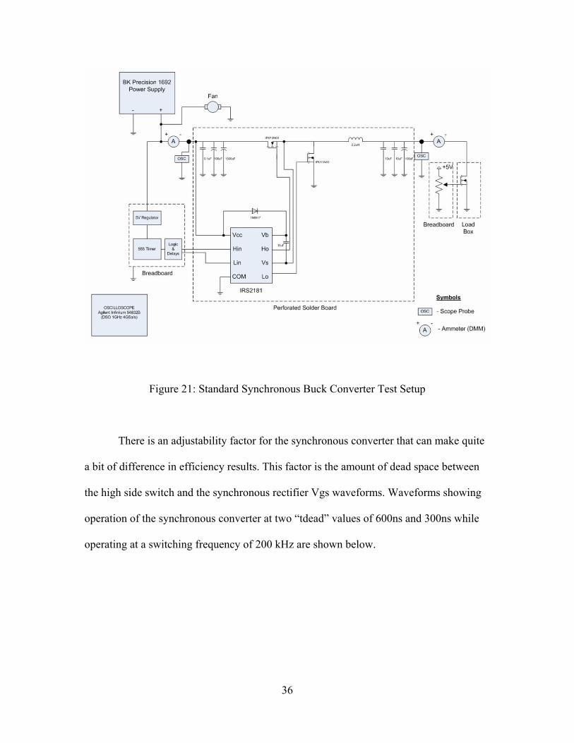
Figure 21: Standard Synchronous Buck Converter Test Setup ........................................ 36
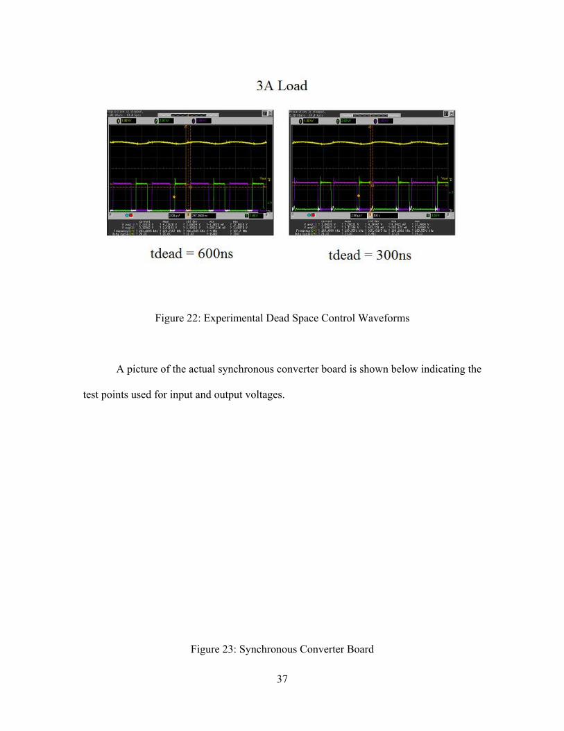
Figure 22: Experimental Dead Space Control Waveforms ............................................... 37

x
Figure 23: Synchronous Converter Board ........................................................................ 37
Figure 24: Standard Buck Converters η vs. Pout Plots ..................................................... 38
Figure 25: Standard Buck Converters Power Loss vs. Pout Plots .................................... 39
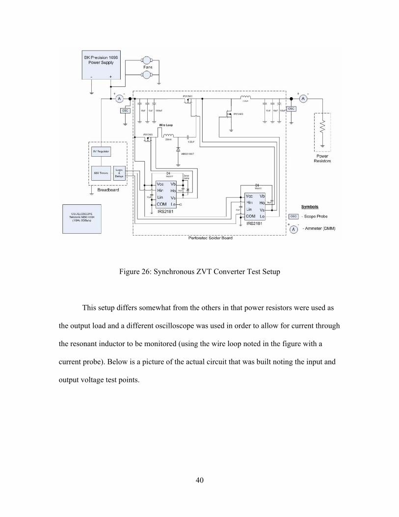
Figure 26: Synchronous ZVT Converter Test Setup ........................................................ 40
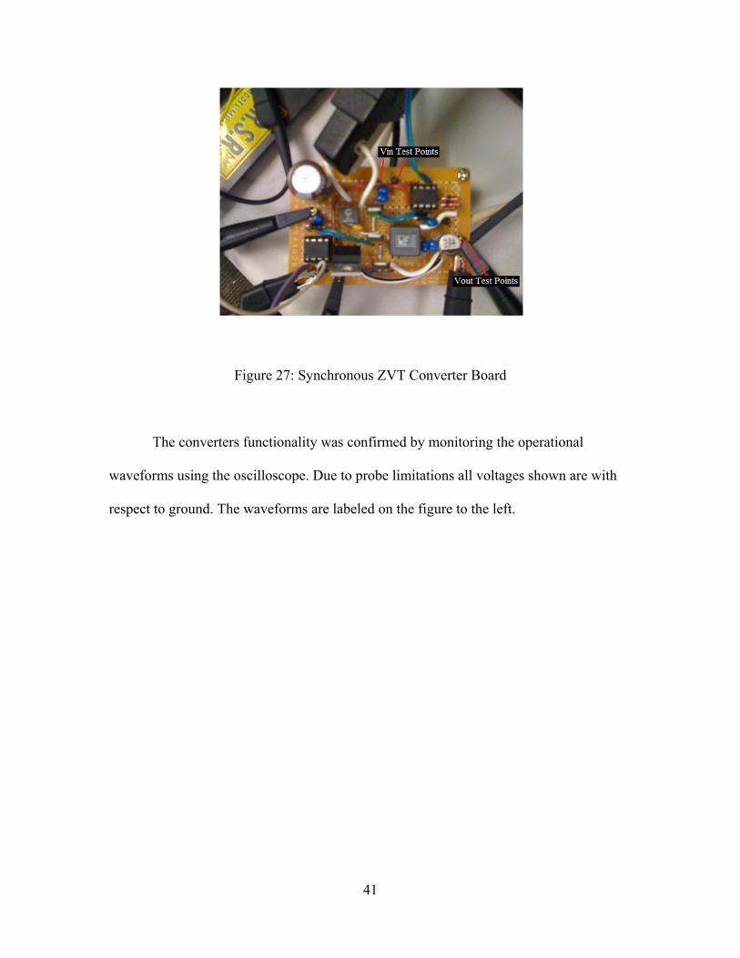
Figure 27: Synchronous ZVT Converter Board ................................................................ 41
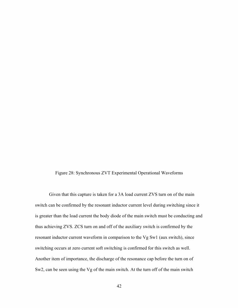
Figure 28: Synchronous ZVT Experimental Operational Waveforms ............................. 42
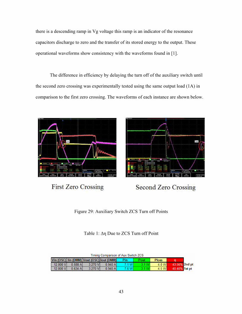
Figure 29: Auxiliary Switch ZCS Turn off Points ............................................................ 43
Figure 30: Synchronous ZVT vs. Synchronous buck Efficiency ..................................... 44
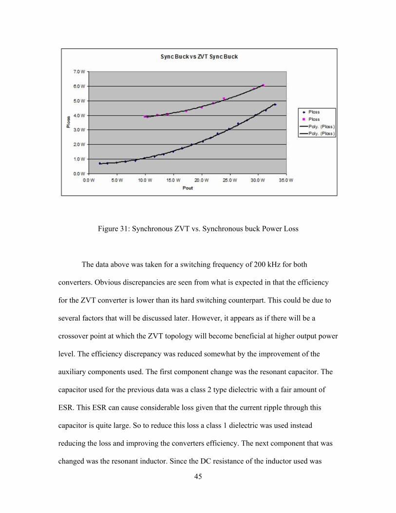
Figure 31: Synchronous ZVT vs. Synchronous buck Power Loss ................................... 45
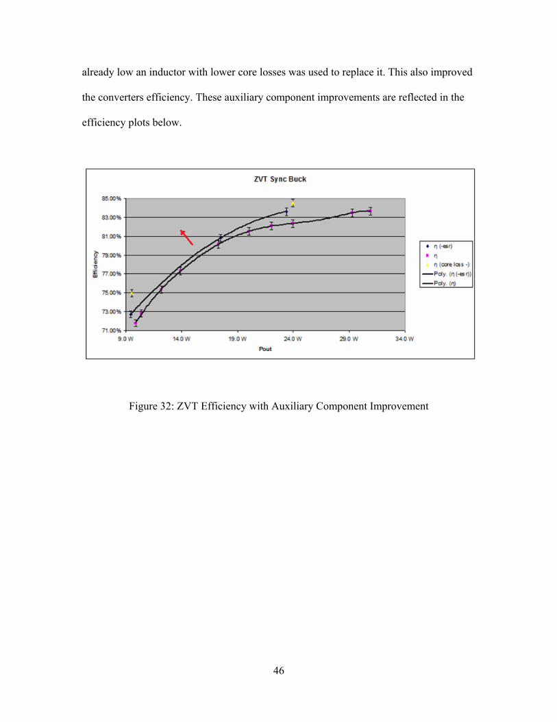
Figure 32: ZVT Efficiency with Auxiliary Component Improvement ............................. 46
Figure 33: ZVT Power Loss with Auxiliary Component Improvement ........................... 47
Figure 34: ZVT η Improvement in Reference to Synchronous Buck ............................... 47
Figure 35: ZVT Ploss Improvement in Reference to Synchronous Buck ........................ 48
Figure 36: Oxide Electron Trapping for Traditional MOSFET Structure ........................ 55
Figure 37: MOSFET Before and After Hot Carrier Ageing ............................................. 57
Figure 38: LDMOS Before and After Hot Carrier Ageing ............................................... 57
Figure 39: Example VDMOS Structure ............................................................................ 59
Figure 40: Synchronous Buck Circuit for ∆Rds(on) Simulation ...................................... 62
Figure 41: Rds(on) Measurement Simulation Circuit ....................................................... 63
Figure 42: MOSFET Out of Circuit Stressing .................................................................. 65
Figure 43: Device Rds(on) Measurement Circuit ............................................................. 66
Figure 44: In Circuit Stressing Setup ................................................................................ 67

xi
LIST OF TABLES
Table 1: ∆η Due to ZCS Turn off Point ............................................................................ 43
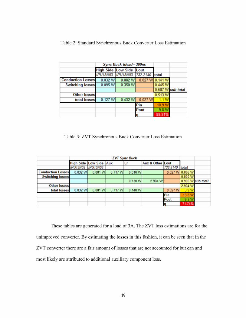
Table 2: Standard Synchronous Buck Converter Loss Estimation ................................... 49
Table 3: ZVT Synchronous Buck Converter Loss Estimation ......................................... 49
Table 4: Simulated ∆Rds(on) Impact on Efficiencies ....................................................... 63
Table 5: Theoretical ∆η due to ∆Rds(on) ......................................................................... 68
Table 6: Rds(on) Before and After Stress (STP22NF03L) ............................................... 70

xii
LIST OF EQUATIONS
Equation 1: · ......................................................................................... 7
Equation 2: .............................................................................................. 10
Equation 3: · · ........................................................................ 11
Equation 4: ∆ · · ·
.......................................................................... 11
Equation 5: ....................................................................... 15
Equation 6: · · ............................................................... 15
Equation 7: · · 1 ..................................................... 16
Equation 8: · · · .............................. 16
Equation 9: ............................................................................. 16
Equation 10: ............................................................................. 16
Equation 11: · · · . · · · ..................... 16
Equation 12: · · ................................................... 16
Equation 13: ............................................. 17
Equation 14: · · ................................................... 17
Equation 15: . ·
..................................... 17
Equation 16: · · · .................................................... 17
Equation 17: ·
............................................................................................... 32
Equation 18: ................................................................ 33

xiii
Equation 19: .................................................................................................. 33

1
CHAPTER 1: INTRODUCTION
1.1 Introduction
The field of Power Electronics is very broad and contains components from
several disciplines of electrical engineering. Being general, Power Electronics involves
converting energy from one form to another [3]. Globally we are becoming more aware
that energy is a precious commodity. Therefore the use of energy is becoming such that
we want more for less, that is, more work done using less energy than before. In essence,
in any system we want energy expended to do the desired job only with no additional
energy expenditures for unwanted or unnecessary work. This concept of high efficiency
is nothing new but the demand for it seems to be growing.
Most Power Electronic systems can be simplified into three general components
the source, converter, and load (shown in the block diagram below). The source provides
the input energy and the load uses that energy to perform the desired task. The load can
be anything from a motor to a microprocessor or a combination of items. In some cases,
only a source and a load make up the entire system. However, in most systems some form
of conversion is needed to provide the load with correct form of energy it needs.
Certainly energy savings in any system, given a source, can be made almost anywhere in
the system. The converter, being central to the energy flow, can be one of the best places
to reduce unwanted losses. The ideal converter does not have any losses and the power in

2
is equal to the power out. In any real converter this is not the case of course and there are
losses. Reducing this loss to a minimum is necessary to have a high level of efficiency.
Figure 1: Simplified Power Electronic System Block Diagram
1.2 Objectives
THESIS MAIN OBJECTIVES
• Providing expanded knowledge of ZVT soft switching buck converters through
application of theory, simulation and experimental testing.
o Using this expanded knowledge and pointing it in a useful direction.
Investigation of this topologies potential use in integrated
applications.
• Analyzing the impacts of device ageing on switching converters using theory and
experimental testing.
o Discuss the various factors that are associated with the effects or lack of
effects in converters.

3
1.3 Motivation
Continued study of power converting circuits is important for improving the
performance and reliability of tomorrow’s converters and by extension, the performance
in terms of power consumption and overall reliability of the systems that they support. It
is with this goal in mind that the research and experimental testing outlined in this paper
was performed.
1.4 Thesis Structure
This thesis is structured as follows. In chapter 2, some foundation for the work to
follow will be provided in the form of some basic knowledge and principals. Chapter 2
contains some fundamental concepts that may be useful in understanding for those not as
familiar to the field of Power Electronics. In chapter 3, the focus is on soft switching
buck converters and the first main objective of this paper will be addressed. In chapter 4,
the focus is shifted to converter ageing effects and the second main objective of this
paper will be addressed. In chapter 5, results from previous chapters will be noted and
conclusions will be made based upon these results.

4
CHAPTER 2: BUCK CONVERTER BACKGROUND INFORMATION
2.1 Power Conversion
Power conversion is in and of itself a general topic, one that is addressed within
the field of Power Electronics. There are four general forms of power converting circuits
ac-to ac, ac-to-dc, dc-to ac, and dc to dc [3] [32]. Since addressing all forms of
conversion would not be entirely useful for supporting the scope of the work done in this
thesis, only dc-to-dc will be covered. Even within topic of dc-to-dc converters there are
many circuit topologies and aspects of each circuit topology that can be addressed, the
very thought of covering them all can be overwhelming. So, to simplify this and try to
provide only what is necessary buck converters will be the main focus. This type of
conversion is very often needed and it is one of the most popularly used.
2.1.1 Purpose
Power conversion in general is used to provide the correct form of energy needed
by the load. Buck converters from a high level description provide a function that is very
basic and necessary for many power systems. They step down the input voltage to a
specified level and provide a level of regulation deemed necessary by the circuit.
5
2.1.2 Switching Mode Power Supplies
Buck type converters are switching mode power supplies, meaning that they use
switching elements within their circuitry to manipulate the voltage and current
characteristics of the output by using energy storage elements. This differs from a linear
regulator that does not use switching elements and simply drops voltage by controlling a
resistive element. The benefit of using a switch mode supply is in efficiency gain. This
gain comes from the use of energy storage elements such as inductors and capacitors
which ideally do not dissipate any energy. A buck converter can be thought of on an
abstract level as a kind of DC transformer, in that it is used to change DC voltage and
current characteristics from input to output similar to an AC transformer.
2.1.3 Loss and Efficiency
When using switching mode power electronic circuits, efficiency is always of
some importance and often is very important. There can be other reasons, but generally a
buck converter is used over a linear regulator mostly for the reason of higher efficiency.
Lower losses and thus higher efficiency save power which is important for energy
conservation. Energy conservation leads to beneficial results such as longer battery life,
and reduced size for applications such as mobile electronic systems.

6
2.2 Non-Isolated Buck Converters
2.2.1 Description
The term non-isolated refers to the presence of a common voltage reference node
between the input and output of the converter. The number of non-isolated buck
converter topologies is still very large but by describing a couple of key topologies it
becomes easier to understand some of the more complex ones.
2.2.2 Standard PWM Topology
Figure 2: Ideal PWM Buck Converter
This is the most basic buck converter and its operation is very well known and
thoroughly described in many texts [3] [32]. Since this is the case, the converter will be
described qualitatively. See references such as [3] [32] for a more in depth description.

7
Figure 3: Standard PWM Buck Converter Modes of Operation
The duty cycle for the high side switch of this converter is used to control the
output voltage with the following relation.
Equation 1: ·
This relation allows for what is known as PWM control. This method of control is
preferred since it is easy to implement and very widely used. Another important aspect of
this converter, to mention, is the inductor’s conduction modes. This converter can operate
in what is called constant conduction mode (CCM) or discontinuous conduction mode or
(DCM) [3]. In CCM the inductor current is always greater than zero as in the figure
below.

8
Figure 4: CCM Operation
9
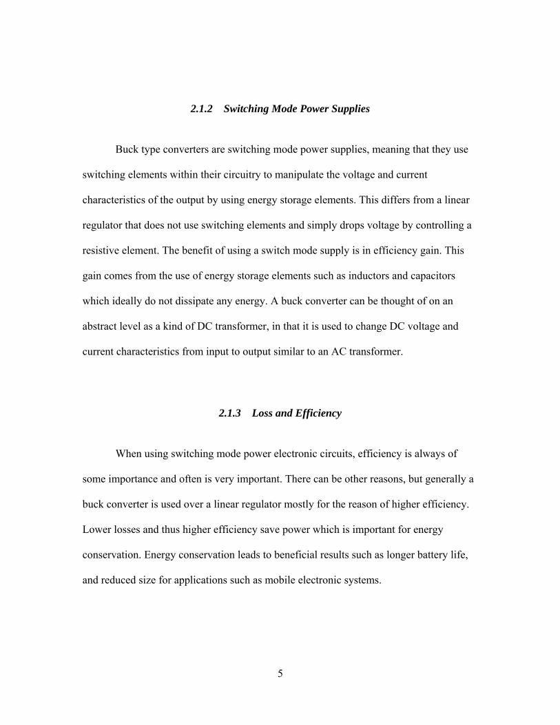
Figure 5: DCM Operation
10
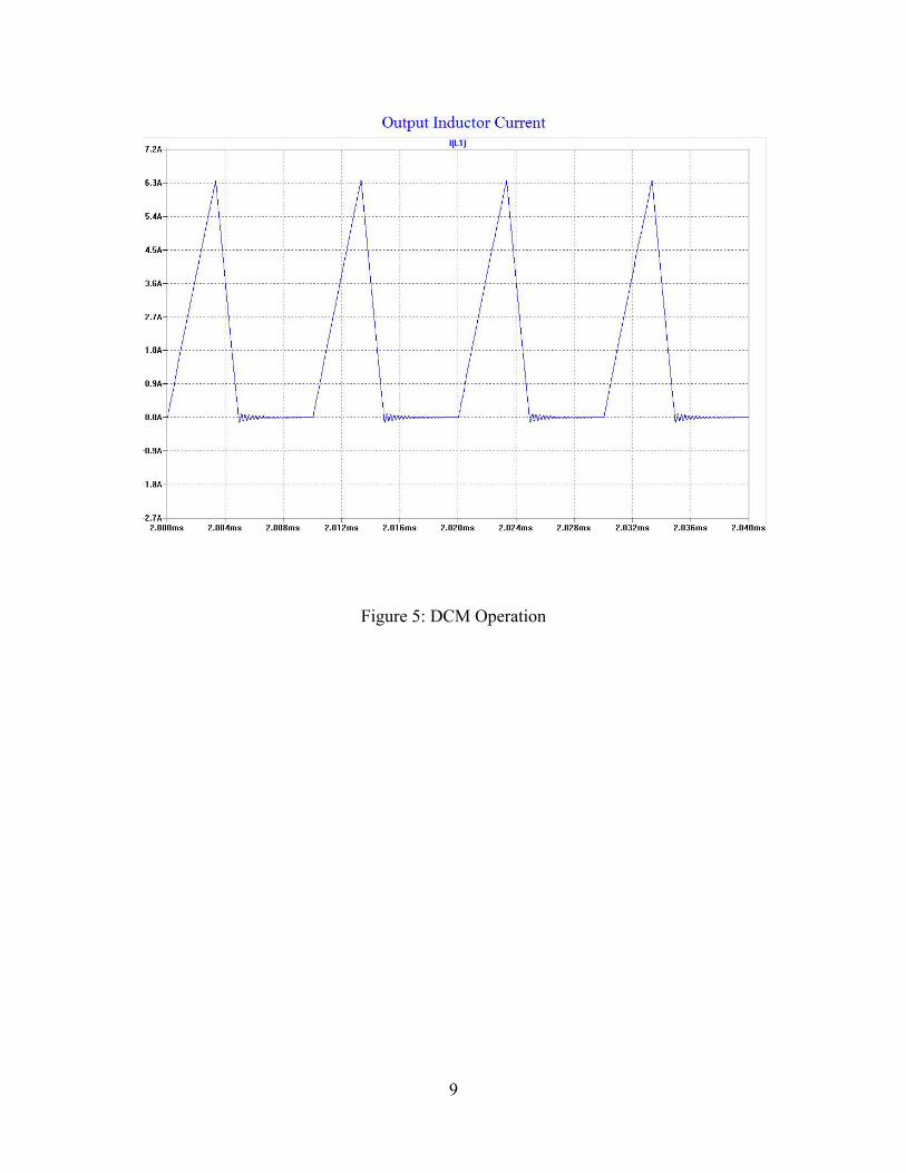
Figure 6: DCM Operation Synchronous Switch with Negative Conduction
In DCM operation the inductor current is zero for a portion of the switching period.
Negative current is also possible if a synchronous switch is used depending on its control,
as shown in the second DCM figure above. Which mode of inductor conduction the
converter is in is controlled by output load level, switching frequency, duty cycle, and
inductance (Lout). For a given switching frequency (Fsw), duty cycle (D), and load (R)
there is what is called a critical inductance value (Lcrit).
Equation 2:

11
Equation 3: · ·
The conduction mode that the inductor is in is important for converter control and
efficiency. Generally CCM is the preferred mode of converter operation since the
converter gain is the simple linear relation as in equation1. In DCM operation the gain
(Vout/ Vin) is not linear and equation 1 does not apply. For PWM controller design linear
voltage gain is best. Also of importance is the magnitude of the voltage ripple generated
at the converters output due to switching. This ripple is dependent on inductance (Lout),
capacitance (Cout), duty cycle (D), and switching frequency (Fsw).
Equation 4: ∆ · · ·
The equations above are important to consider when designing any buck
converter and although more advanced converters may not have the exact same relations
the same general dependences on Lout, and Cout will remain.

12
2.2.3 Synchronous PWM Switching
Figure 7: Ideal Synchronous Buck Converter
Synchronous switching is a method used to reduce converter losses by reducing
the conduction losses sustained in the low side switching device. This means replacing
the low side diode with a switching element such as a MOSFET. Diode losses due to the
forward voltage drop of the p-n junction are greater than the channel conduction loss of a
MOSFET. This is particularly beneficial for low duty cycles since more time is spent
with the low side conducting, with some exceptions due to frequency of operation. This
method adds some complexity to control but it is still PWM. Controlling this circuit
requires two synchronous PWM signals that are inverted in comparison to each other
with what is referred to as dead space or dead time between them.
13
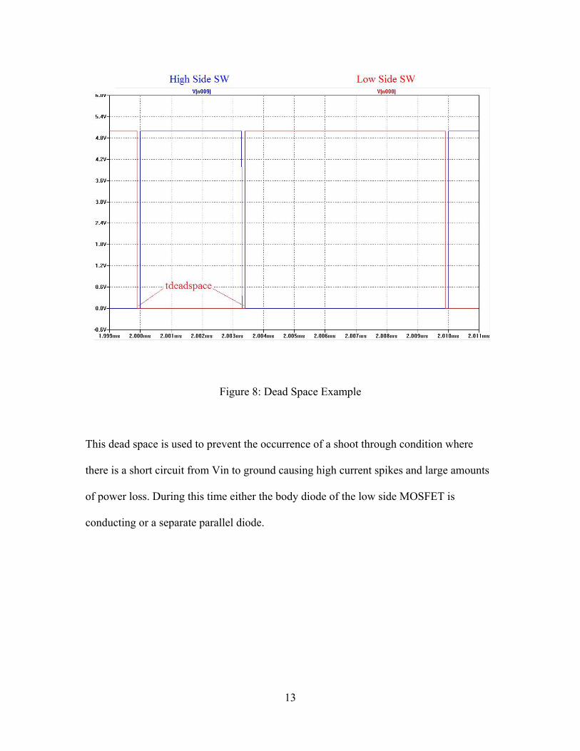
Figure 8: Dead Space Example
This dead space is used to prevent the occurrence of a shoot through condition where
there is a short circuit from Vin to ground causing high current spikes and large amounts
of power loss. During this time either the body diode of the low side MOSFET is
conducting or a separate parallel diode.

14
Figure 9: Ideal Synchronous Buck Converter Conduction Paths
2.3 Converter Losses
2.3.1 Losses in General
Losses can be found in any element of the converter. The amount of loss in each
component depends on the element characteristics and the circuit operational
characteristics. The distribution of loss can vary widely but typically switching elements
15
tend to remain of significant importance. However, the loss in other components cannot
be overlooked.
2.3.2 Switching Element Loss
MOSFETs are very popularly used in most converters so it makes the most since
to use them in the description of switching element loss. The switch losses can be divided
into to general forms of loss, conduction losses and switching losses. These losses are
described in detail below [2]. The calculations used are approximations since the internal
losses of every device cannot be measured during operation. This is a numerical method
based on certain device characteristics with the synchronous buck converter in mind.
Equation 5:
2.3.2.1 Conduction Losses
Conduction losses are defined as losses that are sustained due to the equivalent
resistance of the MOSFET channel after the channel is completely enhanced. This
resistance is the Rds(on) value for the transistor. Estimation of this loss can be made
using the following equations for the high and low side devices.
Equation 6: · ·

16
Equation 7: · · 1
2.3.2.2 Switching Losses
Switching Losses occur during switching transitions as spikes in power are
created due to rising voltage and falling current overlaps and vice versa depending on the
transition occurring. In general these losses occur due to device parasitic capacitances. A
good part of the switching losses sustained are due to the charging and discharging of
these capacitances through larger resistance then are seen during device conduction. The
equations used for estimation of these losses are below.
Equation 8: · · ·
Equation 9:
Equation 10:
Equation 11: · · · . · · ·
Equation 12: · ·

17
Equation 13:
Equation 14: · ·
Equation 15: . ·
Equation 16: · · ·
Note for the low side that equation 11 is used twice to calculate the rising and falling
edge losses. Diode losses during dead space are included as switching losses as well with
equation 16, these losses are often lumped with the low side switching losses since it
typically is the low side MOSFET’s body diode conducting. There are additional losses,
due to the gate drive that are typically insignificant unless the switching frequency
becomes extremely high, that not stated here [2].
2.3.3 Other Loss
Losses, as stated previously can be found in any element in the converter. Losses
are found in both input and output capacitances due to the ESR (equivalent series
resistance). Losses in the inductor (Lout) are in two forms those due to the DCR (direct
current resistance) and core losses associated with the inductor core material. Any of
these losses can become significant given the right conditions so they should not be

18
overlooked. Other additional losses such as control circuitry losses are typically small
enough to be neglected. For upcoming converters to be discussed additional components
are added, these components create loss that can be estimated similarly.

19
CHAPTER 3: NON-ISOLATED ZVT BUCK CONVERTER STUDY
3.1 Introduction
A large amount of work has been done on this topic since it was first introduced
[15]. New topologies within this genre continue to spring up looking to improve upon
this concept [1] [17-23] and move on to ever more efficient and power dense converters.
To understand the work that has been done, some soft switching basic concepts must be
explained. First of all, the reason soft switching is done in the first place needs to be
understood. The next important thing to understand is how soft switching is
accomplished. This leads into ZVT’s contributions to this goal and looking more into the
present, how newer ZVT topologies may help us better accomplish the goals of soft
switching by improving upon this concept even further.
The driving force behind the development of soft switching topologies is the
demand for high power density converters, which means more power handling capability
in a smaller package. Typically a large amount of area used by a converter is occupied by
the passive energy storage elements such as the output inductor and capacitor in a buck
converter. This is due to the fact that for a given switching frequency, to reduce voltage
and current ripple larger values of inductance and capacitance are used. Larger passive
component values tend to be physically larger in size, thus taking up more area. To
combat this for a given set of output voltage and load conditions the switching frequency
can be increased allowing for the use of smaller component values. As switching
frequency is increased so too are the converter’s switching losses. At high frequencies
switching losses can become the dominate loss in a converter. So the battle between
20
efficiency and area become more obvious. In order to save area high frequencies are
desired, however at higher frequencies switching loss can cause a considerable drop in
efficiency. Thus a creation of a need to reduce switching losses is present and soft
switching topologies have sought to fulfill this need the best way possible.
3.2 ZVS, ZCS, & ZVT Description
Understanding how soft switching is accomplished is important in understanding
how to use the topologies that achieve this goal. Soft switching topologies make use of
additional circuit elements passive or active in order to limit di/dt or dv/dt during
switching and minimize current and voltage overlap to reduce switching losses [30].
Essentially, in the switching device at the switching interval, either the current or the
voltage must be driven to zero to bring the product of the two as close to zero as possible.
This leads to the concepts of zero voltage switching (ZVS) and zero current switching
(ZCS). Just as in the name either the voltage or current is driven to zero during switching.
There are many topologies that use ZVS, ZCS, or both to reduce overall switching losses.
Converters such as the ones termed as quasi-resonant can be used to achieve ZVS or ZCS
[3] [16]. However, converters such as these can cause additional problems that offset soft
switching benefits, such as additional voltage or current stress on the main switch [30].
Converters that have soft switching but reduce or eliminate this stress are more highly
desirable. For this reason, what are known as zero voltage transition (ZVT) converters
have become very popular and as stated previously, the number of ZVT topologies that
have been introduced is large. ZVT converters accomplish soft switching while
21
minimizing additional stresses associated with other previous topologies. In the next two
sub sections these concepts will be explained through examples.
3.2.1 ZVS/ ZCS
ZVS and ZCS switching topologies typically use resonance to bring the voltage or
current in the switch to zero. In ZVS converters if a MOSFET is used, often this is
accomplished by flowing current in the reverse direction through the body diode just
before switching occurs, thus discharging the parallel capacitance of the switch bringing
the voltage across it near zero before turn on. At turn off this parallel capacitance limits
the dv/dt across the switch and causes a reduction current voltage overlap. In ZCS
converters typically a resonance inductor placed in series with the switch is used to
resonant the current through the switch to zero for turn off and limit di/dt for turn on [3]
[16]. As an example of this simulation of a ZVS buck converter topology will be used
below.
22
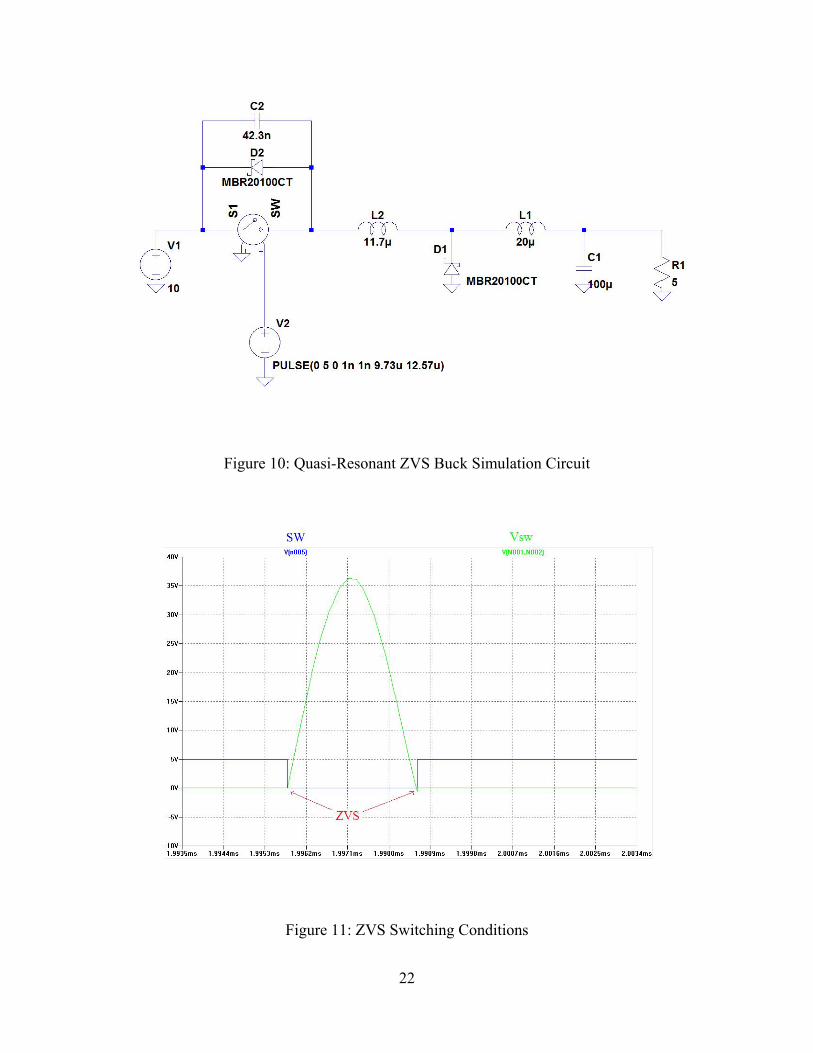
Figure 10: Quasi-Resonant ZVS Buck Simulation Circuit
Figure 11: ZVS Switching Conditions

23
The circuit used in the above LTSpice simulation is based on a quasi-resonance
type ZVS converter [3] [16]. The waveforms shown are the switch voltage in green (this
would typically be the Vds if a MOSFET were to replace the ideal switch) and the
switching turn on and of waveform in blue (replace with Vgs for MOSFET). These
waveforms demonstrate ZVS turn on and turn off for the switch. As can be seen a much
larger voltage stress (approximately 3.6 times more) is applied across the switch then is
seen for the standard PWM topology. This additional stress limits the devices that can be
used to ones that typically have a larger Rds(on), thus creating more conduction losses.
The additional conduction losses associated with this larger Rds(on) can offset any
performance gains made by soft switching. Additionally this topology is a frequency
modulated topology and not a PWM topology. This can cause some additional
complications in implementation.
3.2.2 ZVT
There are many types of ZVT converters. This class of converters has been
categorized more thoroughly into various types in [30]. However, in general there are two
types of ZVT converters, ones that use passive auxiliary circuit elements only such as in
[21] and ones that use active elements in the auxiliary circuit [1] [17-20] [23]. Active
types will be the only ones discussed to follow. Although there are many different
topologies that use ZVT the basic concept can explained by using the buck topology from
[15]. This family of topologies is typically considered to be the conventional ZVT
24
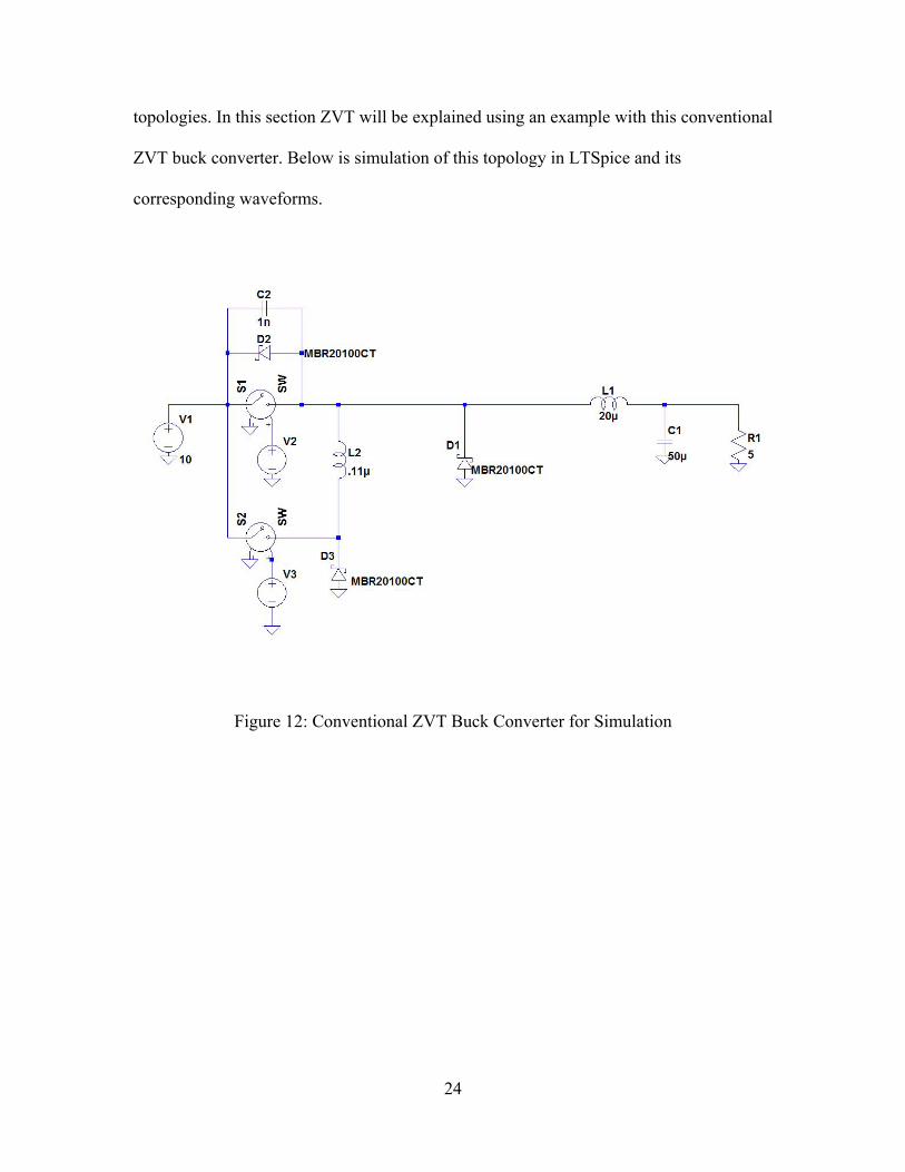
topologies. In this section ZVT will be explained using an example with this conventional
ZVT buck converter. Below is simulation of this topology in LTSpice and its
corresponding waveforms.
Figure 12: Conventional ZVT Buck Converter for Simulation
25
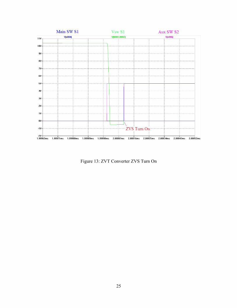
Figure 13: ZVT Converter ZVS Turn On

26
Figure 14: ZVT Converter ZVS Turn Off
The above simulation waveforms show that zero voltage turn on and off is
achieved by this topology without inducing additional voltage stress on the main switch.
This improvement allows for the use of lower rated switching elements that typically
have lower Rds(on) values. However this topology is not without its drawbacks. The
auxiliary switching elements induce some undesired losses, in particular there are still
switching losses in the auxiliary switch. Hard switching in this switch creates additional
switching losses that can lower the converters overall efficiency. Most recently ZVT
topologies have turned their focus to include the elimination of switching losses in the

27
auxiliary switch as well, some even looking to virtually eliminate all losses associated
with switching [1] [17-23].
3.3 Synchronous ZVT Topology of Interest
3.3.1 Description and Reasoning
Figure 15: ZVT Synchronous Buck Converter
This converter topology is one that has recently been introduced into the category
of ZVT switching converters [1]. This converter’s operation allows for soft switching to
occur in all switches used. This is a benefit not included in previous ZVT topologies such
as [15]. Some of those that have included auxiliary switch soft switching, have added
quite a large amount of complexity to the converter. This converters design is fairly
simplified when compared to others [17] [23]. This synchronous ZVT topology will be
used for the analysis to follow. The main interest of ZVT is increase power density so it
logically follows that this type of converter being low loss in nature and almost entirely

28
devoid of switching losses may be a candidate for use in application such as integration,
similar to converters in [14] [24-27].In order to see if this converter may be suitable for
such applications further insight is required. It is with this interest in mind that the
research done on this converter was carried out.
3.3.2 Operational Simulation
The operation of this converter is described in detail in [1]. Simulation was
performed to show its operation in LTSpice.
Figure 16: Synchronous ZVT Topology Simulation Circuit

29
Figure 17: Synchronous ZVT Important Waveforms
The above operational waveforms are consistent with the ones described in [1]
with one difference. The turn of switch one has been slightly delayed in order to improve
the efficiency of the converter. This will be explained in the description to follow. Below
are the switching waveforms confirming soft switching.

30
Figure 18: Synchronous ZVT Converter Main Switch ZVS
31
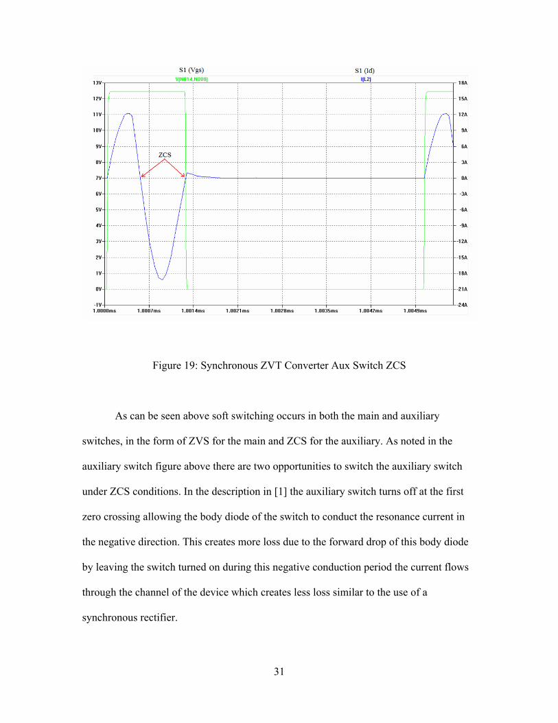
Figure 19: Synchronous ZVT Converter Aux Switch ZCS
As can be seen above soft switching occurs in both the main and auxiliary
switches, in the form of ZVS for the main and ZCS for the auxiliary. As noted in the
auxiliary switch figure above there are two opportunities to switch the auxiliary switch
under ZCS conditions. In the description in [1] the auxiliary switch turns off at the first
zero crossing allowing the body diode of the switch to conduct the resonance current in
the negative direction. This creates more loss due to the forward drop of this body diode
by leaving the switch turned on during this negative conduction period the current flows
through the channel of the device which creates less loss similar to the use of a
synchronous rectifier.

32
3.3.3 Design Considerations
ZVT Voltage and load testing conditions used for experimentation to follow were
similar to those used in [1]. However, there are some important things to consider when
using topology in general. First of all, as with other ZVT topologies the period of
resonance between auxiliary components Lr and Cr should be small in comparison to the
overall switching period. This is done in order to limit the auxiliary circuit’s effects on
gain and efficiency. PWM gain is still desired since it is linear and the smaller the
resonance period is the more linear ZVT’s gain is as well. Efficiency can also benefit
from this as the smaller the time the auxiliary components spend conducting the smaller
their conduction loss. The frequency and consequent resonance period of these auxiliary
components is designed using the following equation.
Equation 17: ·
Although this equation dictates the product of Lr and Cr the exact values of each
are not specified by it. In order to pick the specific values of Lr and Cr input voltage and
output load conditions must be considered. In order to accomplish ZVS soft switching in
the main switch the magnitude of the resonance current through Lr must exceed the load
output current. This is to induce the current flow through the device body diode necessary
to create a ZVS turn on condition. Further detail is given in the circuit mode descriptions
in [1] and can be used to better understand this concept. Below are the two equations
used to determine the designed values of Lr and Cr.

33
Equation 18:
Equation 19:
Equation 19 is the characteristic impedance. By using the equation for Lr
resonance current (equation 18) it can be seen that for a given input voltage (Vin) the
magnitude of this current can be controlled using the characteristic impedance (Z). This is
important in the converter’s design since the magnitude of resonance current essentially
dictates the maximum load at which the converter is operating with complete soft
switching conditions, keeping in mind that iLr should be greater than load current. There
are several other design considerations, with most of the basic outlined in [1], but this is
one of the most important. Proper timing of the switching waveforms is also important
and must be considered in the design.
3.4 Results/ Discussion
This section includes a summary of the experimentation that was performed using
this converter. This experimentation was carried out with the intention of being a
platform for further investigation of this topology for application such as integration.
Three converters were designed, built, and tested both standard synchronous and non-
synchronous buck converters as well as the ZVT synchronous buck converter. Efficiency
versus load data was taken for all three converters.
34
Some additional details are stated to eliminate any confusion. Parts used were
kept as consistent as possible between converters in order to make as fair a comparison as
possible. All converters were driven with an external bread boarded PWM. Gate drivers
for switches were on board. Control was open loop and waveform timing was adjusted
manually via potentiometer controls. This was done to allow for maximum adjustability
of the converters in terms of waveform control, power stage components, conversion
levels, and load conditions. Since converter characteristics were so dynamic, design of
closed loop controls would have proved restrictive and time consuming. Voltage
conversion for all converters to follow is from 12V to 3.3V unless otherwise noted. Any
differences in converter setups should be noted on the particular setup as they are
described.
3.4.1 Standard Buck Converters
To serve as a baseline for efficiency both synchronous and non-synchronous
standard (hard switching) converters were built and tested. The test setup for both
converters is shown below.

35
Figure 20: Standard Non-Synchronous Buck Converter Test Setup
36
Figure 21: Standard Synchronous Buck Converter Test Setup
There is an adjustability factor for the synchronous converter that can make quite
a bit of difference in efficiency results. This factor is the amount of dead space between
the high side switch and the synchronous rectifier Vgs waveforms. Waveforms showing
operation of the synchronous converter at two “tdead” values of 600ns and 300ns while
operating at a switching frequency of 200 kHz are shown below.
37
Figure 22: Experimental Dead Space Control Waveforms
A picture of the actual synchronous converter board is shown below indicating the
test points used for input and output voltages.
Figure 23: Synchronous Converter Board

38
Experimental results were obtained for these converters at an operating frequency
of 200 kHz. The experimental results for efficiency testing of these converters are
summarized in the efficiency and power loss plots below. The results are consistent with
what is expected.
Figure 24: Standard Buck Converters η vs. Pout Plots

39
Figure 25: Standard Buck Converters Power Loss vs. Pout Plots
3.4.2 Synchronous ZVT Topology
The synchronous ZVT converter was built using the same main switching
components as the standard buck converters (MOSFET part IPU13N03) but of course
additional components were needed to serve as the auxiliary circuit components. Its test
setup is shown below.
40
Figure 26: Synchronous ZVT Converter Test Setup
This setup differs somewhat from the others in that power resistors were used as
the output load and a different oscilloscope was used in order to allow for current through
the resonant inductor to be monitored (using the wire loop noted in the figure with a
current probe). Below is a picture of the actual circuit that was built noting the input and
output voltage test points.
41
Figure 27: Synchronous ZVT Converter Board
The converters functionality was confirmed by monitoring the operational
waveforms using the oscilloscope. Due to probe limitations all voltages shown are with
respect to ground. The waveforms are labeled on the figure to the left.
42
Figure 28: Synchronous ZVT Experimental Operational Waveforms
Given that this capture is taken for a 3A load current ZVS turn on of the main
switch can be confirmed by the resonant inductor current level during switching since it
is greater than the load current the body diode of the main switch must be conducting and
thus achieving ZVS. ZCS turn on and off of the auxiliary switch is confirmed by the
resonant inductor current waveform in comparison to the Vg Sw1 (aux switch), since
switching occurs at zero current soft switching is confirmed for this switch as well.
Another item of importance, the discharge of the resonance cap before the turn on of
Sw2, can be seen using the Vg of the main switch. At the turn off of the main switch
43
there is a descending ramp in Vg voltage this ramp is an indicator of the resonance
capacitors discharge to zero and the transfer of its stored energy to the output. These
operational waveforms show consistency with the waveforms found in [1].
The difference in efficiency by delaying the turn off of the auxiliary switch until
the second zero crossing was experimentally tested using the same output load (1A) in
comparison to the first zero crossing. The waveforms of each instance are shown below.
Figure 29: Auxiliary Switch ZCS Turn off Points
Table 1: ∆η Due to ZCS Turn off Point

44
Since the circuit is operating in DCM the efficiency above is very low, however
the clear difference in power loss of 0.5 W can be seen confirming power loss savings
made by switching on the second ZCS turn off point. This second ZCS switching point is
used in all analysis to follow.
Experimental efficiency results were obtained and the synchronous ZVT
efficiency was compared to the efficiency of the standard synchronous converter below.
Figure 30: Synchronous ZVT vs. Synchronous buck Efficiency
45
Figure 31: Synchronous ZVT vs. Synchronous buck Power Loss
The data above was taken for a switching frequency of 200 kHz for both
converters. Obvious discrepancies are seen from what is expected in that the efficiency
for the ZVT converter is lower than its hard switching counterpart. This could be due to
several factors that will be discussed later. However, it appears as if there will be a
crossover point at which the ZVT topology will become beneficial at higher output power
level. The efficiency discrepancy was reduced somewhat by the improvement of the
auxiliary components used. The first component change was the resonant capacitor. The
capacitor used for the previous data was a class 2 type dielectric with a fair amount of
ESR. This ESR can cause considerable loss given that the current ripple through this
capacitor is quite large. So to reduce this loss a class 1 dielectric was used instead
reducing the loss and improving the converters efficiency. The next component that was
changed was the resonant inductor. Since the DC resistance of the inductor used was
46
already low an inductor with lower core losses was used to replace it. This also improved
the converters efficiency. These auxiliary component improvements are reflected in the
efficiency plots below.
Figure 32: ZVT Efficiency with Auxiliary Component Improvement

47
Figure 33: ZVT Power Loss with Auxiliary Component Improvement
Figure 34: ZVT η Improvement in Reference to Synchronous Buck

48
Figure 35: ZVT Ploss Improvement in Reference to Synchronous Buck
By improving the auxiliary components (i.e. reducing their losses) an overall
power loss and efficiency improvement can be seen. It appears that the previously
projected crossover point may happen earlier. In an attempt to analyze the location of the
additional losses, power loss estimation by component can be done using the equations
from chapter 2. The tables below are used to estimate some of the losses.
49
Table 2: Standard Synchronous Buck Converter Loss Estimation
Table 3: ZVT Synchronous Buck Converter Loss Estimation
These tables are generated for a load of 3A. The ZVT loss estimations are for the
unimproved converter. By estimating the losses in this fashion, it can be seen that in the
ZVT converter there are a fair amount of losses that are not accounted for but can and
most likely are attributed to additional auxiliary component loss.

50
3.5 Conclusions
Soft switching can be used to improve converter performance. However several
factors come into play that can influence the benefits of soft switching. Examples of these
factors are power semiconductor technology, switching frequency, and power range [30].
Based on the data obtained it seems that for the given components, switching frequency,
load range, and other operating characteristics that the benefits of ZVT are outweighed by
the additional losses induced. By operating at a fairly low switching frequency and using
switching components that have inherently low switching losses, ZVT’s benefits might
be overshadowed at this load range. As stated previously, it appears that perhaps outside
of this load range there may be benefits but due to measurement limitations a higher load
range could not be tested. Another factor that could be contributing to the discrepancy in
the efficiency data could be the length of the resonance period used in this design. The
resonance period length could be reduced leading to smaller conduction losses and
perhaps higher efficiencies. Although this converter does not prove beneficial over its
standard hard switching counterpart this shows that several circuit factors, as stated in
[30], can come into play when determining if ZVT will be of benefit for use.
Increasing the switching frequency should better show the benefits of this
topology for a given set of components. In future testing, using components that allow for
high frequency operation, much more aggressive switching frequencies can be tested and
the results at these higher frequencies can be compared to give indication of this
topologies potential usefulness in applications such as integration. In the next section
there is some discussion about integrated converter applications and this topologies
potential in such applications.
51
3.6 Integrated Converter Discussion
The demand for converters to shrink further and further in size has brought on
several new converter designs that are completely on chip [14] [24-26] or vary near to
totally on chip [27]. These converters operate at extremely high frequencies when
compared to their discrete component counterparts. This high frequency is sure to cause
some fairly significant switching loss. Since frequencies are sometimes very high ZVS
transitions can sometimes come for free, so to speak, since the intrinsic parallel
capacitance of the devices can cause ZVS turn off conditions. This depends greatly on the
individual case. Turn on, on the other hand is still typically hard switching so this leaves
room for improvement. Although this room for improvement can be filled by topologies
such as the ZVT topology mentioned in [1], there are other complications that may offset
any benefits of using a topology such as this in integrated applications, namely front end
device losses [25]. Front end device loss has only been mentioned in passing up to this
point because at lower frequencies this loss is rather insignificant. Front end loss refers to
the losses incurred by driving the device gate. These losses occur in the gate driver as
well as in the MOSFET gate itself. In order to drive the gate both high and low the gate
capacitance is charged and discharged through finite resistance values. The rapid charge
and discharge of gate capacitances can cause significant energy loss even for fairly small
gate capacitances. Since the topology presented in [1] has more active devices that must
tolerate power stage level stresses, losses such as these may prove problematic depending
on how high the switching frequency is for the converter. Depending on the frequency
52
and components, operating at the typical light loads associated with integrated converters
may also prove problematic for maximizing ZVT’s benefits. The light loads due to
limitations of current are typically set by current density limitations due to conductor
thickness in integrated inductors. As such the more pressing issues for fully integrated
converters may be found in the output inductor. Topologies that use interleaving of
inductors can partially aid in this dilemma [24] [29].
The issues in the full integration of buck converters are numerous and several
solutions are being offered by newer topologies. However it seems that integrated
converters will always be fundamentally limited in their ability to deliver large amounts
of power but it is not to be said that there is no room for improvement. Topologies using
ZVT methods should not be counted out for potential use in the improvement of such
converters.

53
CHAPTER 4: NON-ISOLATED SYNCHRONOUS BUCK CONVERTER STRESS EFFECTS
4.1 Introduction
In this chapter the focus is shifted to a much different issue then the previous
chapter. The issue of device ageing effects on standard non-isolated synchronous buck
converters will be explored in detail. Device ageing and device stress are directly related.
By controlling the stress applied on a device one can control the rate at which a device
degrades. Increasing the stress in the appropriate manner can be used as a tool to
theoretically project normal degradation over long periods of time (ageing effects). The
main goal in this chapter is to illustrate how a method of this type may be used for
showing the effects that MOSFET ageing can have on power electronic circuits,
specifically synchronous buck converters.
In order to effectively accomplish this goal, first some background information
about hot carrier effects will be mentioned. Then the converters operational
characteristics effect on the converters susceptibility to ageing effects will be mentioned
as well. The methods used in an attempt to experimentally confirm the theory in this
chapter will be described in detail. Finally the results for both experimentation as well as
simulation will be shown and conclusions about this data will be made.
54
4.2 Hot Electron Device Degradation
4.2.1 Description
Hot carrier degradation at the device level has been fairly well documented and
experimental validation of this theory has been performed [5] [7-10]. The magnitude and
impacts of this degradation on circuit level applications have been studied for digital
circuits and some analog applications such as RF circuitry in the past [6]. Only recently
has consideration been turned to possible effects on power electronics applications such
as switching mode power supplies like buck converters [4]. Before moving to the higher
level effects and experimental results, some description of the theory is in order.
The following description applies to the traditional lateral MOSFET structure.
The mechanisms that cause device degradation for the traditional MOSFET structure are
fairly simple to explain and understand given a basic knowledge of semiconductor
devices. To explain these mechanisms the figure below will be used for reference. Hot
carriers actually degrade MOSFETs with the combined effects of two mechanisms,
damage to the oxide-substrate interface causing lower mobility at the surface region and
creation of trapped charge. Given the following conditions for an nmos, Vgs > Vth so
that a channel is formed beneath the oxide and Vds > 0V so that current will flow from
drain to source (Id> 0A), it is possible for hot electron degradation to occur on some
level. However, effects are greatly dependent on the magnitude and direction of the
electric field in the device. The effects are greatest when Vgs is large relative to Vth and

55
close to the value of Vds so the electric field looks somewhat like in the figure below.
The horizontal component of the electric field is the desired component, in that it causes
carriers (electrons) to flow from source to drain. The vertical component is necessary to
create the channel in the first place but has a secondary undesired effect. The vertical
component of the electric field tends to cause the carriers, electrons in this case, to stay
near the surface at the oxide interface increasing the chance of interfacial lattice damage
as well as the chances that an electron will have enough energy to exceed the energy
barrier necessary to enter the oxide [7]. When an electron enters the oxide it will either be
swept to the gate by the electric field causing gate current or become trapped at neutral
centers in the oxide causing oxide charging [6] [7]. Both interface damage and trapped
charge create changes in devices characteristics that are described in the next section.
Figure 36: Oxide Electron Trapping for Traditional MOSFET Structure

56
4.2.2 Effects on Device Characteristics
Interface damage and trapped charge create changes in device characteristics that
can be undesirable for circuit operation. As mentioned previously interface damage
lowers the carrier mobility at the surface near the interface. The surface damage tends to
increase the channels effective resistance by partially impeding the carrier’s path through
the channel along the interface. Trapped charge in the oxide will cause changes in Vth,
the direction of the change depends on the type of carriers that are injected into the oxide,
hot electrons or hot holes. In the case of nmos shown in the figure above hot electrons are
injected in the oxide, this injection effect is also referred to as oxide charging. Oxide
charging in the case of hot electron injection will cause Vth to increase. This trapped
negative charge tends increase the gate charge for a given bias condition increasing the
gate capacitance values, such as the gate to source capacitance. The figure below
illustrates the effects mentioned on a standard MOSFET cross section by showing the
device at a given biasing condition before (left) and after (right) hot carrier ageing.
57
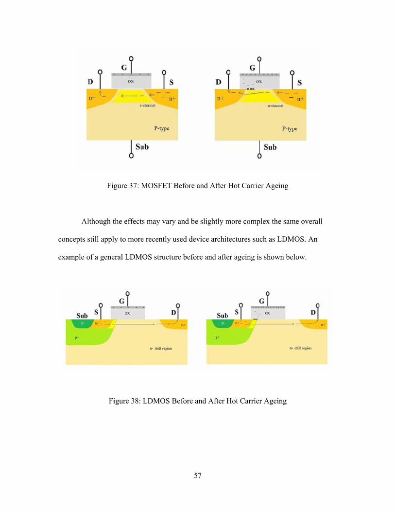
Figure 37: MOSFET Before and After Hot Carrier Ageing
Although the effects may vary and be slightly more complex the same overall
concepts still apply to more recently used device architectures such as LDMOS. An
example of a general LDMOS structure before and after ageing is shown below.
Figure 38: LDMOS Before and After Hot Carrier Ageing

58
4.2.3 Effects Pertaining to Power Electronic Circuits
With switching mode power supplies aside from reliability and proper regulation
often high efficiency is paramount. Since power efficiency is generally important it is
desirable to keep component losses to a minimum. Keeping this in mind, much of the
time a large portion of the total losses of a converter can be found in the switching
devices such as MOSFETs. This makes the switching device of key importance to
converter design. So, it logically follows that degradation in device characteristics that
cause additional losses should result in circuit efficiency degradation. If the effects are
confirmed, it then becomes a question of how much degradation occurs.
Focusing in on power losses due to MOSFET devices in power converter
applications, as stated previously one can find two main categories of losses, conduction
losses and switching losses. Since for switching converters the MOSFET is typically
trying to fill the role of an ideal switch there are two modes generally, on and off. For
MOSFETs, conduction losses occur when the switch is turned on. Conduction losses for
MOSFET devices is mainly caused by Rds(on) or effective resistance of the device
during conduction (equations 6 & 7). Switching losses are losses that occur during the
switches transition from off to on and vice versa. Switching losses can be comprised of a
combination of different effects caused by the MOSFETs characteristics and circuit
conditions but in general switching losses are highly influenced by the devices gate
charge (as in equations 8 & 11). Since hot carrier ageing can affect both Rds(on) and Qg
it is worth investigating device ageing effects for switching power supplies.
59
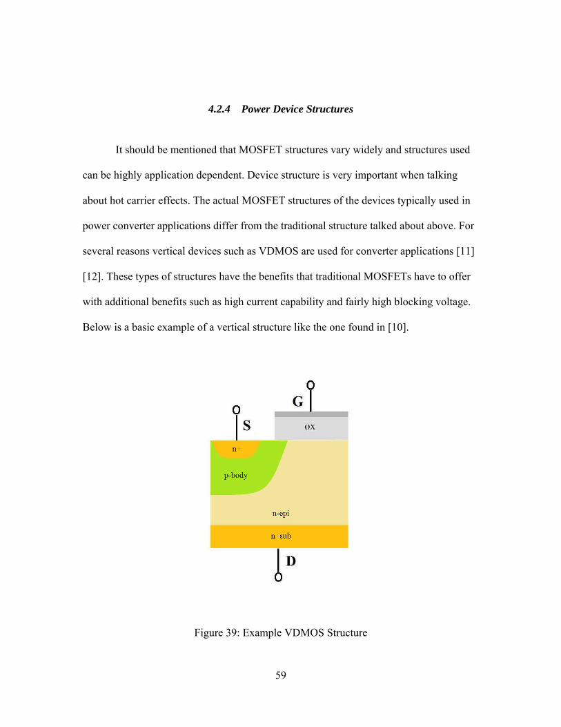
4.2.4 Power Device Structures
It should be mentioned that MOSFET structures vary widely and structures used
can be highly application dependent. Device structure is very important when talking
about hot carrier effects. The actual MOSFET structures of the devices typically used in
power converter applications differ from the traditional structure talked about above. For
several reasons vertical devices such as VDMOS are used for converter applications [11]
[12]. These types of structures have the benefits that traditional MOSFETs have to offer
with additional benefits such as high current capability and fairly high blocking voltage.
Below is a basic example of a vertical structure like the one found in [10].
Figure 39: Example VDMOS Structure

60
Vertical device structures are typically considered to be fairly immune to hot
electron ageing since the flow of carriers is in the vertical direction and mostly avoids the
oxide silicon interface. However there have been studies showing that at least some of
these structures can show degradation due to the hot electron effect [10]. This is an
important thing to consider since vertical silicon devices are prominent in applications
such as the synchronous buck converter. They are used not only for the benefits offered
but also since they are mature technology. Other newer technologies are being developed
such as GaN HEMTs [13].These and other non-silicon technologies may see more
widespread use in the future but for now, especially for integrated applications, silicon
based technology is dominate.
4.2.5 Modeling/ Simulating Effects
Although the impact of ageing may vary with device structure, modeling can be
done similarly for all structures since it is the overall device characteristic changes that
are of concern. The non-isolated synchronous buck converter is a good topology to look
at for this investigation since it is such a widely used and easy to implement topology.
The following sections will be specifically focusing on the synchronous buck converter.
As was mentioned before, this is a well known and widely used topology, which makes it
a good choice for use in this study. Nmos devices are typically the switching element of
choice for this converter topology. As went over in chapter 2, power losses can be
estimated using some key parameters from the MOSFET [2].

61
Modeling the effects of hot electron ageing can be done both at the device and
circuit level fairly easily. At the device level, the parameters that are affected can be
modified in the model. The two parameters to adjust are Vt (threshold voltage) and μ
(carrier mobility). By changing these parameters appropriately, device ageing can be
modeled. This device model can then be used in circuit to compare the losses before and
after device ageing. If access to these parameters is unavailable it is possible to at least
partially model simulate these changes using circuit conditions alone. Simulation such as
the latter will be used for obtaining results in the sections to follow.
4.3 Susceptibility of Converters
In order to determine if a converter’s efficiency is susceptible to ageing effects,
the switching device used must show hot electron ageing susceptibility and the converter
itself must operate such that the level of degradation developed in the device has a
significant effect on the level of power loss in the converter. In short both device and
circuit must be susceptible to degradation. To clarify what is meant by this some more
explanation is needed.
Device susceptibility, as mentioned previously, is structure dependent as well as
biasing dependent. Some structures are highly resistant to ageing effects while others
tend to degrade more easily. Lateral devices with the oxide silicon interface parallel to
carrier flow are typically more susceptible to degradation. Lateral structures such as these
are not typically used for converters except for some novel cases with integration in mind
[14]. Vertical structures typically used tend to be less susceptible but can degrade
62
similarly [10]. If devices are robust to ageing then it is less likely that significant changes
in efficiency will occur for a given converter. On the other hand, if the devices do show
degradation efficiency change becomes more circuit level dependent.
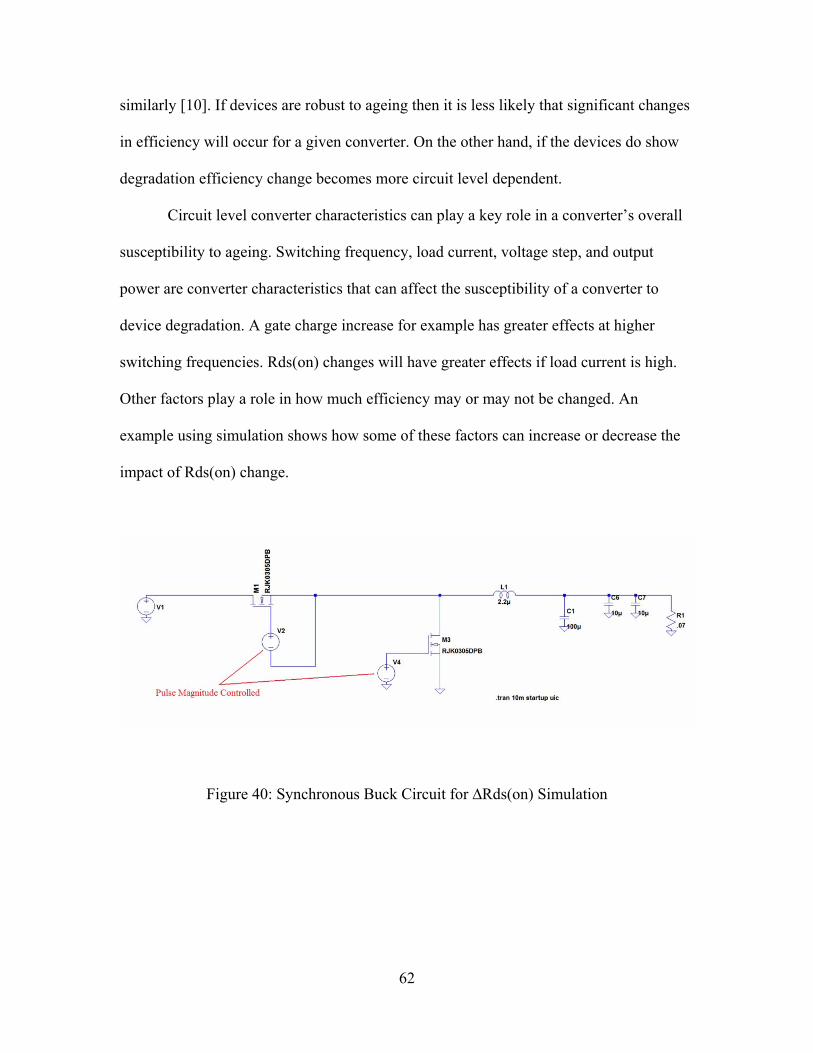
Circuit level converter characteristics can play a key role in a converter’s overall
susceptibility to ageing. Switching frequency, load current, voltage step, and output
power are converter characteristics that can affect the susceptibility of a converter to
device degradation. A gate charge increase for example has greater effects at higher
switching frequencies. Rds(on) changes will have greater effects if load current is high.
Other factors play a role in how much efficiency may or may not be changed. An
example using simulation shows how some of these factors can increase or decrease the
impact of Rds(on) change.
Figure 40: Synchronous Buck Circuit for ∆Rds(on) Simulation

63
Figure 41: Rds(on) Measurement Simulation Circuit
Simulation was done using LTSpice in order to show how converter
characteristics can effect a given change in Rds(on) effect on efficiency. Different pulse
magnitudes were used as Vgs gate drives in order to achieve different Rds(on) values.
The Rds(on) was changed by 20% for each simulation shown in the table below. Rds(on)
was measured using a sub circuit simulation. As shown in the table converters with high
current relative to Vout and larger impacts of conduction loss will have greater efficiency
changes for a given Rds(on) change.
Table 4: Simulated ∆Rds(on) Impact on Efficiencies

64
This example illustrates that although a device’s Rds(on) might degrade greatly a
measurable change in efficiency may or may not manifest itself depending on the
converters sensitivity to this change.
4.4 Experimental Simulation of Device Ageing
4.4.1 Methods of Stressing
In order to attempt to experimentally induce accelerated ageing voltage stresses
that are much higher than the typical must be applied to the MOSFET devices in an
attempt to create a high internal electric field. Methods of stressing and there actual
effects on the device become somewhat difficult to identify when using off the shelf
discrete MOSFET parts as was done to follow but with the simple goal of inducing some
measurable device Rds(on) degradation in mind stressing experimentation was carried
out. However it was unknown whether any results showing degradation would occur and
not knowing device cross sections proves problematic to this goal.
4.4.2 Out of Circuit Stressing
The most controlled method of stressing was out of circuit testing in which the
device was stressed separately from the synchronous buck converter in order to achieve a
measurable Rds(on) change and then replaced in circuit to show its effects on efficiency
(similar to stressing performed in [10]). Two devices have been stressed using this
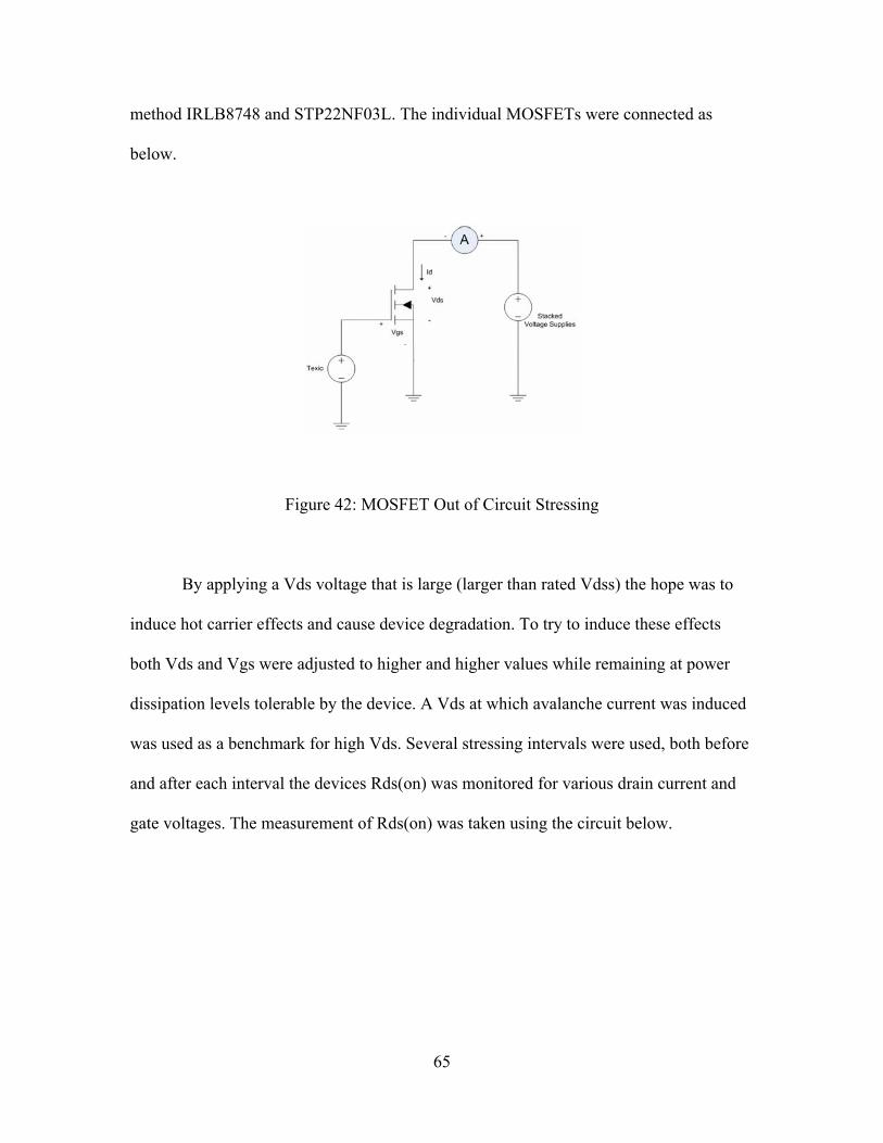
65
method IRLB8748 and STP22NF03L. The individual MOSFETs were connected as
below.
Figure 42: MOSFET Out of Circuit Stressing
By applying a Vds voltage that is large (larger than rated Vdss) the hope was to
induce hot carrier effects and cause device degradation. To try to induce these effects
both Vds and Vgs were adjusted to higher and higher values while remaining at power
dissipation levels tolerable by the device. A Vds at which avalanche current was induced
was used as a benchmark for high Vds. Several stressing intervals were used, both before
and after each interval the devices Rds(on) was monitored for various drain current and
gate voltages. The measurement of Rds(on) was taken using the circuit below.
66
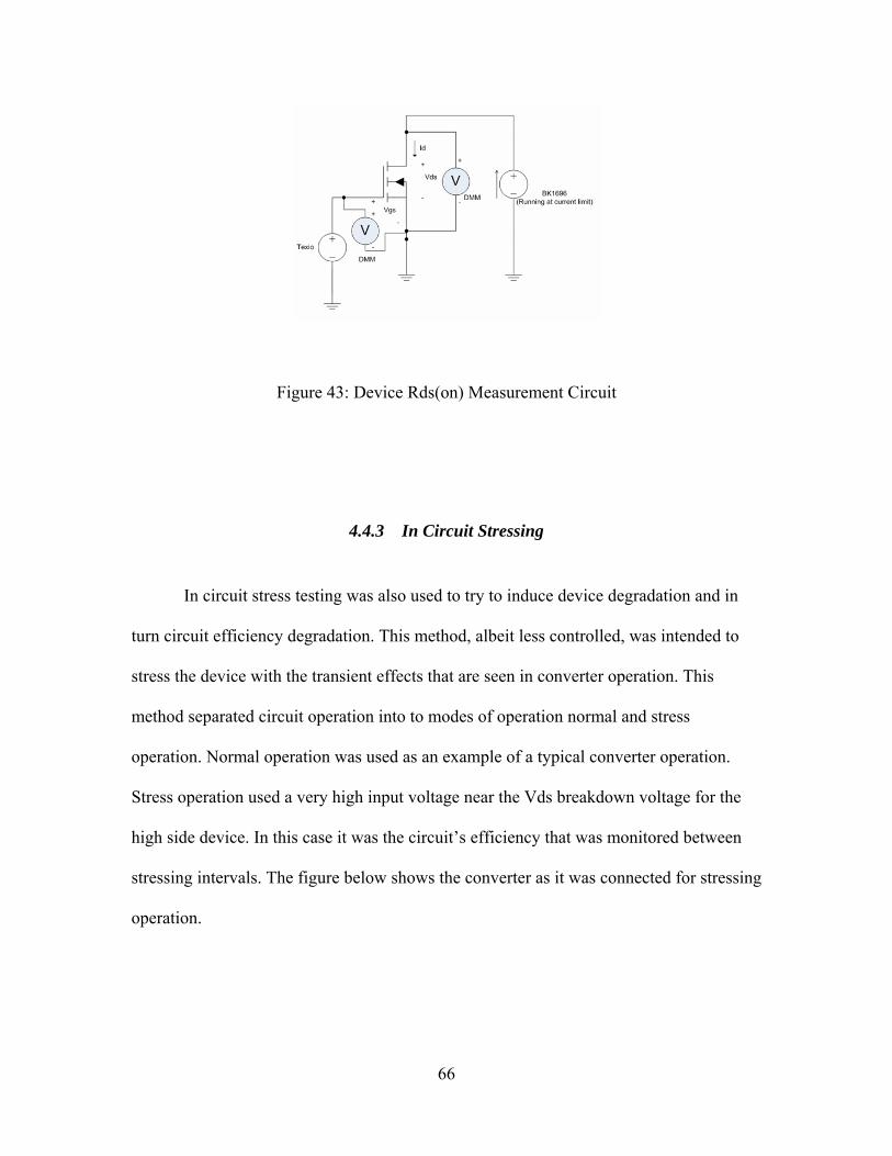
Figure 43: Device Rds(on) Measurement Circuit
4.4.3 In Circuit Stressing
In circuit stress testing was also used to try to induce device degradation and in
turn circuit efficiency degradation. This method, albeit less controlled, was intended to
stress the device with the transient effects that are seen in converter operation. This
method separated circuit operation into to modes of operation normal and stress
operation. Normal operation was used as an example of a typical converter operation.
Stress operation used a very high input voltage near the Vds breakdown voltage for the
high side device. In this case it was the circuit’s efficiency that was monitored between
stressing intervals. The figure below shows the converter as it was connected for stressing
operation.
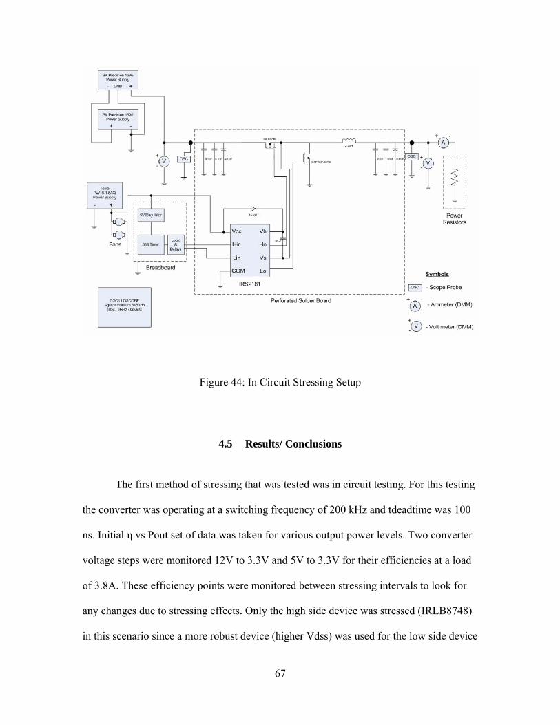
67
Figure 44: In Circuit Stressing Setup
4.5 Results/ Conclusions
The first method of stressing that was tested was in circuit testing. For this testing
the converter was operating at a switching frequency of 200 kHz and tdeadtime was 100
ns. Initial η vs Pout set of data was taken for various output power levels. Two converter
voltage steps were monitored 12V to 3.3V and 5V to 3.3V for their efficiencies at a load
of 3.8A. These efficiency points were monitored between stressing intervals to look for
any changes due to stressing effects. Only the high side device was stressed (IRLB8748)
in this scenario since a more robust device (higher Vdss) was used for the low side device

68
(IXTP100N04T2). The high side device’s breakdown voltage was measured prior to
stressing and was found to be approximately 31.2V. Many stressing intervals were used
incrementing the input voltage each time. The maximum level of stress applied was
32.5V for a time period of 60 minutes using a stressing operation duty cycle of 10% with
a load current of 0.33A. Stressing using this method was found to be ineffective, at least
for the scenarios that were tested. The efficiency of the converter never changed out of
the experimental error. This method, although trying to mimic the actual circuit operation
of the converter, is not particularly accurate to the types of stressing that may actually
occur in the devices over time. For this reason continued stress testing was done out of
circuit. For this testing there are also issues with the converters level of sensitivity to
changes in Rds(on) as shown in the table below.
Table 5: Theoretical ∆η due to ∆Rds(on)
This table uses the actual experimentally measured efficiency and power loss data
and the estimated loss due to Rds(on) and projects the effects of an increase of 20% in
Rds(on). As can be seen in the table the change in efficiency would be minimal. This
result is insensitive to ∆Rds(on) showing insignificant efficiency changes due to Rds(on).

69
However, in a more positive light this result shows that a converter of this type would be
very robust to any changes in Rds(on) if they did occur.
With circuit susceptibility being a factor the converter characteristics were
changed to a 5V to 0.7V with a load of 10A. This converter showed susceptibility to
Rds(on) changes in simulation and could prove useful in showing efficiency changes
better. In order to assure that Rds(on) was indeed changing a more direct out of circuit
approach is needed.
After in circuit stress testing proved ineffective in inducing degradation the
approach of out of circuit testing was taken. The previous device used in circuit
(IRLB8748) was stressed out of circuit as well using the method stated in the above
section. Its Rds(on) was measured for several different gate voltages and drain currents
prior to and after stressing intervals. Several stress intervals were applied to this device.
For this device and method no significant degradation was seen outside of experimental
measurement error. A second device (STP22NF03L) was also stressed similarly. This
device’s breakdown voltage was found experimentally to be approximately 35.4V. Again
several stress intervals were impressed upon this device. The maximum stress interval
applied to this device was a Vds of 36V at a Vgs of 2V with Id = 30 mA for a time
interval of 12 hrs. As can be seen in the table below no significant changes occurred in
the Rds(on) of this device either, as all changes are inside experimental error.

70
Table 6: Rds(on) Before and After Stress (STP22NF03L)
As stated previously the effectiveness of stressing methods is difficult to analyze
correctly without knowing the specific device architecture. With the given, off the self
devices, and the methods used no degradation was able to be produced. This indicates
that either the devices are robust to hot electron effects or the methods of stressing were
ineffective. For vertical devices it is typically accepted that there is immunity or at least a
very high level of resistance to hot electron effects. Vertical symmetrical structures such
as the ones found in [11] can be particularly resistant to hot electron effects due to the
reduction of localized high electric field. At least some vertical devices have displayed
some susceptibility to hot electron effects [10] and with this in mind further investigation
may prove useful. Using different devices and perhaps adjusted methodology, the hot
electron effect may still have effects on some converters.

71
CHAPTER 5: CONCLUSIONS AND FUTURE WORK
5.1 Conclusions
In this thesis current topics relevant to buck converters have been brought up and
addressed through theory, simulation, and experimentation. Two specific topics were
focused on, ZVT topology analysis and possible future uses such as integration and the
possible effects due to long term converter stressing. Thus far framework for continued
study of ZVT’s potential for integration has been laid down. Experimental testing using a
discrete approach was done for this topology leaving further study of more aggressive
switching frequencies typical for integration open to continue. Converter stress effects
have been gone over and discussed thoroughly. Although theory may suggest a window
of possibility for these effects to occur, experimentation has yet to reveal any possible
threats to converter performance. The potential for these effects has yet to be proven.
Future work in both topics is of interest.
5.2 Future Work
Future work may include continued study and testing of ZVT topologies specific
to integration (i.e. very high frequency and components smaller in size). Also, continued
study of converter stressing to either confirm or deny the presence of significant ageing
effects in buck converters.

72
REFERENCES [1] S. Pattnaik, A. K. Panda, Aroul K., K. K. Mahaptara, “Experimental Validation of A Novel Zero Voltage Transition Synchronous Buck Converter,” in Proc. TENCON 2008 IEEE Region 10 Conf. 2008, pp. 1-6. [2] Jon Klein, “Synchronous buck MOSFET loss calculations with Excel model,” Product and Technical Information/ Design Resources www.fairchildsemi.com , January 4, 2006 [3] I. Batarseh: Power Electronic Circuits, John Wiley & Sons, New York, 2004. [4] J. S. Yuan, “Evaluation of Hot-Electron Effect on LDMOS Device and Circuit Performances,” IEEE Transactions on Electron Devices, Vol. 55, No. 6, June 2008 [5] H. Wang, M. Davis, H. De, S. Bibyk, Y. Nissan-Cohen, “Transient Hot-Electron Effect on N-Channel Device Degradation,” IEEE Conf. 1989, pp. 79-82. [6] R. J. Baker: CMOS Circuit Design, Layout, and Simulation, Revised Second Edition, John Wiley & Sons, Hoboken, New Jersey, 2008. [7] R. F. Pierret: Semiconductor Device Fundamentals, Addison-Wesley, 1996. [8] S. L. Von Bruns, R. L. Anderson, “Hot Electron-Induced Interface State Generation in n-Channel MOSFET’s at 77K,” IEEE Transactions on Electron Devices, Vol. ED-34, NO. 1, January 1987. [9] R. Versari, A. Pieracci, “Experimental Study of Hot-Carrier Effects in LDMOS Transistors,” IEEE Transactions on Electron Devices, Vol. 46, NO. 6, June 1999. [10] P. Moens, G. Van den bosch, G. Groeseneken, D. Bolognesi, “A Unified Hot Carrier Degradation Model for Integrated Lateral and Vertical nDMOS Transistors,” in Proc. ISPSD ’03. 2003 IEEE 15th International Symposium on, Power Semiconductor Devices and IC’s. 2003, pp. 88-91. [11] H. P. E. Xu, O. P. Trescases, I. -S. M. Sun, D. Lee, W. T. Ng, K. Fukumoto, A. Ishikawa, Y. Furukawa, H. Imai, T. Naito, N. Sato, S. Tamura, K. Takasuka, T. Kohno, “Design of a rugged 60 V VDMOS transistor,” IET Circuits Devices Syst., 2007, 1, (5), pp. 327-331. [12] B. Jayant Baliga, “Trends in Power Semiconductor Devices,” IEEE Transactions on Electron Devices, Vol. 43, NO. 10, October 1996.

73
[13] W. Saito, T. Nitta, Y. Kakiuchi, Y. Saito, K. Tsuda, I. Omura, M. Yamaguchi, “A 120-W Boost Converter Operation Using a High- Voltage GaN-HEMT,” IEEE Electron Device Letters, Vol. 29, NO. 1, January 2008. [14] A. Emira, F. Carr, H. Elwan, R. H. Mekky, “ High Voltage Tolerant Integrated Buck Converter in 65nm 2.5V CMOS,” ISCAS 2009, IEEE International Symposium on, Circuits and Systems, 2009, pp. 2405 – 2408. [15] G. Hua, C.-S. Leu, Y. Jiang, F. C. T. Lee, “Novel Zero- Voltage- Transition PWM Converters,” IEEE Transactions on Power Electronics, Vol. 9, NO. 2, March 1994. [16] K.-H. Liu, F. C. Y. Lee, “Zero- Voltage Switching Technique in DC/DC Converters,” IEEE Transactions on Power Electronics, Vol. 5, NO. 3, July 1990. [17] W. Huang, X. Gao, S. Bassan, G. Moschopoulos, “Novel dual auxiliary circuits for ZVT-PWM converters,” Can. J. Elect. Comput. Eng., Vol. 33, NO. 3/4, Summer/Fall 2008. [18] E. Adib, H. Farzanehfard, “Family of isolated zero-voltage transistion PWM converters,” IET Power Electron., 2008, Vol. 1, NO. 1, pp. 144-153. [19] E. Adib, H. Farzanehfard, “Zero- Voltage- Transistion PWM Converters With Synchronous Rectifier,” IEEE Transactions on Power Electronics, Vol. 25, NO. 1, January 2010. [20] E. Adib, H. Farzanehfard, “New Zero Voltage Transition PWM Converters,” ICIT2006, IEEE International Conference on, Industrial Technology, 2006, pp. 801-806. [21] S. Pattnaik, A. K. Panda, K. K. Mahapatra, “Efficiency Improvement of Synchronous Buck Converter by New Passive Auxiliary Circuit,” TENCON 2008, IEEE Region 10 Conference, 2008, pp. 1-6. [22] L. Shi, L. Chen, C. Yin, “A Novel PWM Soft Switching DC-DC Converter,” INTELEC ’06, 28th Annual International, Telecommunications Energy Conf., 2006, pp. 1-6. [23] M. L. Martins, H. Pinheiro, J. R. Pinheiro, H.A. Gründling, H.L. Hey, “Family of improved ZVT PWM converters using a self-commutated auxiliary network,” IEE Proc.-Electr. Power Appl., Vol. 150, NO. 6, November 2003. [24] J. Wibben, R. Harjani, “ A High-Efficiency DC-DC Converter Using 2 nH Integrated Inductors,” IEEE Journal of Solid-State Circuits, Vol. 43, NO. 4, April 2008.

74
[25] M. Alimadadi, S. Sheikhaei, G. Lemieux, S. Mirabbasi, W. G. Dunford, P. R. Palmer, “A Fully Integrated 660 MHz Low-Swing Energy-Recycling DC-DC Converter,” IEEE Transactions on Power Electronics, Vol. 24, NO. 6, June 2009. [26] W.-R. Liou, M.-L. Yeh, Y. L. Kuo, “A High Efficiency Dual-Mode Buck Converter IC For Portable Applications,” IEEE Transactions on Power Electronics, Vol. 23, NO. 2, March 2008. [27] N. Wang, T. O’Donnell, R. Meere, F. M. F. Rhen, S. Roy, S. C. O’Mathuna, “Thin- Film-Integrated Power Inductor on Si and Its Performance in a 8-Mhz Buck Converter,” IEEE Transactions on Magnetics, Vol. 44, NO. 11, November 2008. [28] Y.-C. Chuang, Y.-L. Ke, “High-Efficiency and Low-Stress ZVT-PWM DC-to-DC Converter for Battery Charger,” IEEE Transactions on Industrial Electronics, Vol. 55, NO. 8, August 2008. [29] W. Li, X. He, “A Family of Isolated Interleaved Boost and Buck Converters With Winding-Cross-Coupled Inductors,” IEEE Transactions on Power Electronics, Vol. 23, NO. 6, November 2008. [30] M. L. Martins, J. L. Russi, H. L. Hey, “Zero-voltage transition PWM converters: a classification methodology,” IEE Proc.-Electr. Power Appl. Vol. 152, NO. 2, March 2005. [31] T. Dyer, J. McGinty, A. Strachan, C. Bulucea, “Monolithic Integration of Trench Vertical DMOS (VDMOS) Power Transistors into a BCD Process,” Proc. ISPSD ’05, The 17th International Symposium on, Power Semiconductor Devices and IC’s, 2005, pp. 47-50. [32] P. T. Krein: Elements of Power Electronics, Oxford University Press, New York, NY, 1998.