
Wireless PWM control of a parallel DC-DC buck converter
7
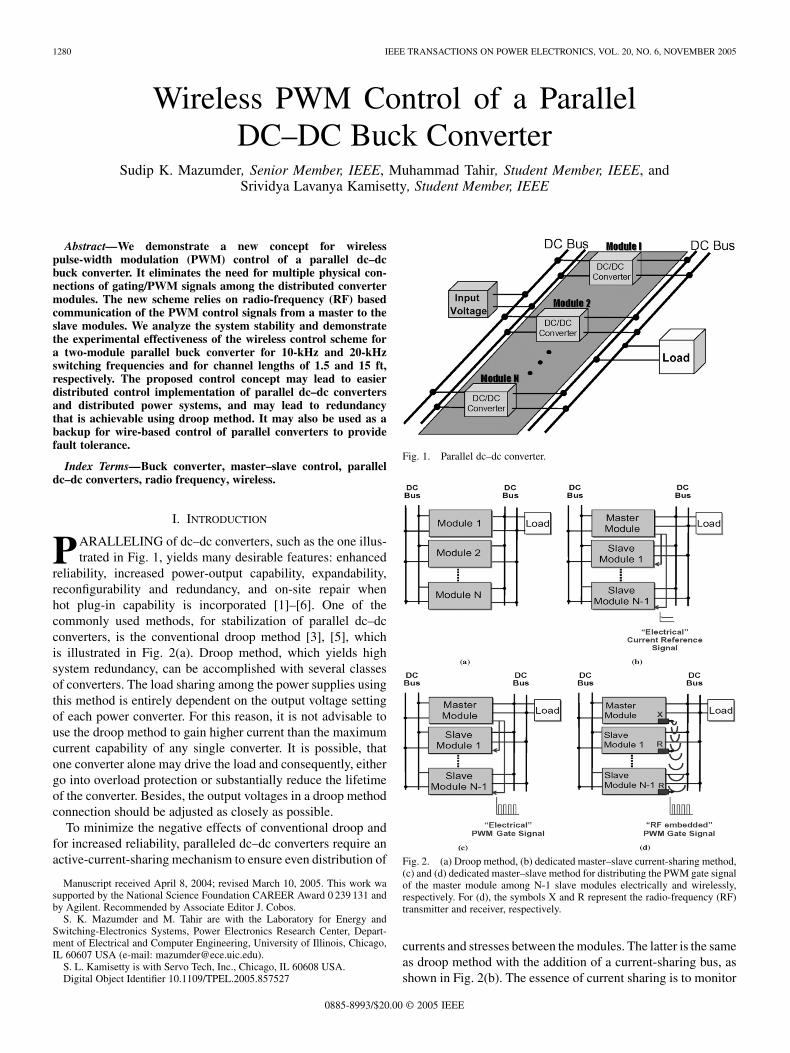
1280 IEEE TRANSACTIONS ON POWER ELECTRONICS, VOL. 20, NO. 6, NOVEMBER 2005 Wireless PWM Control of a Parallel DC–DC Buck Converter Sudip K. Mazumder, Senior Member, IEEE, Muhammad Tahir, Student Member, IEEE, and Srividya Lavanya Kamisetty, Student Member, IEEE Abstract—We demonstrate a new concept for wireless pulse-width modulation (PWM) control of a parallel dc–dc buck converter. It eliminates the need for multiple physical con- nections of gating/PWM signals among the distributed converter modules. The new scheme relies on radio-frequency (RF) based communication of the PWM control signals from a master to the slave modules. We analyze the system stability and demonstrate the experimental effectiveness of the wireless control scheme for a two-module parallel buck converter for 10-kHz and 20-kHz switching frequencies and for channel lengths of 1.5 and 15 ft, respectively. The proposed control concept may lead to easier distributed control implementation of parallel dc–dc converters and distributed power systems, and may lead to redundancy that is achievable using droop method. It may also be used as a backup for wire-based control of parallel converters to provide fault tolerance. Index Terms—Buck converter, master–slave control, parallel dc–dc converters, radio frequency, wireless. I. INTRODUCTION P ARALLELING of dc–dc converters, such as the one illus- trated in Fig. 1, yields many desirable features: enhanced reliability, increased power-output capability, expandability, reconfigurability and redundancy, and on-site repair when hot plug-in capability is incorporated [1]–[6]. One of the commonly used methods, for stabilization of parallel dc–dc converters, is the conventional droop method [3], [5], which is illustrated in Fig. 2(a). Droop method, which yields high system redundancy, can be accomplished with several classes of converters. The load sharing among the power supplies using this method is entirely dependent on the output voltage setting of each power converter. For this reason, it is not advisable to use the droop method to gain higher current than the maximum current capability of any single converter. It is possible, that one converter alone may drive the load and consequently, either go into overload protection or substantially reduce the lifetime of the converter. Besides, the output voltages in a droop method connection should be adjusted as closely as possible. To minimize the negative effects of conventional droop and for increased reliability, paralleled dc–dc converters require an active-current-sharing mechanism to ensure even distribution of Manuscript received April 8, 2004; revised March 10, 2005. This work wa supported by the National Science Foundation CAREER Award 0 239 131 and by Agilent. Recommended by Associate Editor J. Cobos. S. K. Mazumder and M. Tahir are with the Laboratory for Energy and Switching-Electronics Systems, Power Electronics Research Center, Depart- ment of Electrical and Computer Engineering, University of Illinois, Chicago, IL 60607 USA (e-mail: [email protected]). S. L. Kamisetty is with Servo Tech, Inc., Chicago, IL 60608 USA. Digital Object Identifier 10.1109/TPEL.2005.857527 Fig. 1. Parallel dc–dc converter. Fig. 2. (a) Droop method, (b) dedicated master–slave current-sharing method, (c) and (d) dedicated master–slave method for distributing the PWM gate signal of the master module among N-1 slave modules electrically and wirelessly, respectively. For (d), the symbols X and R represent the radio-frequency (RF) transmitter and receiver, respectively. currents and stresses between the modules. The latter is the same as droop method with the addition of a current-sharing bus, as shown in Fig. 2(b). The essence of current sharing is to monitor 0885-8993/$20.00 © 2005 IEEE
-
Upload
independent -
Category
Documents
-
view
0 -
download
0
Transcript of Wireless PWM control of a parallel DC-DC buck converter
1280 IEEE TRANSACTIONS ON POWER ELECTRONICS, VOL. 20, NO. 6, NOVEMBER 2005
Wireless PWM Control of a ParallelDC–DC Buck Converter
Sudip K. Mazumder, Senior Member, IEEE, Muhammad Tahir, Student Member, IEEE, andSrividya Lavanya Kamisetty, Student Member, IEEE
Abstract—We demonstrate a new concept for wirelesspulse-width modulation (PWM) control of a parallel dc–dcbuck converter. It eliminates the need for multiple physical con-nections of gating/PWM signals among the distributed convertermodules. The new scheme relies on radio-frequency (RF) basedcommunication of the PWM control signals from a master to theslave modules. We analyze the system stability and demonstratethe experimental effectiveness of the wireless control scheme fora two-module parallel buck converter for 10-kHz and 20-kHzswitching frequencies and for channel lengths of 1.5 and 15 ft,respectively. The proposed control concept may lead to easierdistributed control implementation of parallel dc–dc convertersand distributed power systems, and may lead to redundancythat is achievable using droop method. It may also be used as abackup for wire-based control of parallel converters to providefault tolerance.
Index Terms—Buck converter, master–slave control, paralleldc–dc converters, radio frequency, wireless.
I. INTRODUCTION
PARALLELING of dc–dc converters, such as the one illus-trated in Fig. 1, yields many desirable features: enhanced
reliability, increased power-output capability, expandability,reconfigurability and redundancy, and on-site repair whenhot plug-in capability is incorporated [1]–[6]. One of thecommonly used methods, for stabilization of parallel dc–dcconverters, is the conventional droop method [3], [5], whichis illustrated in Fig. 2(a). Droop method, which yields highsystem redundancy, can be accomplished with several classesof converters. The load sharing among the power supplies usingthis method is entirely dependent on the output voltage settingof each power converter. For this reason, it is not advisable touse the droop method to gain higher current than the maximumcurrent capability of any single converter. It is possible, thatone converter alone may drive the load and consequently, eithergo into overload protection or substantially reduce the lifetimeof the converter. Besides, the output voltages in a droop methodconnection should be adjusted as closely as possible.
To minimize the negative effects of conventional droop andfor increased reliability, paralleled dc–dc converters require anactive-current-sharing mechanism to ensure even distribution of
Manuscript received April 8, 2004; revised March 10, 2005. This work wasupported by the National Science Foundation CAREER Award 0 239 131 andby Agilent. Recommended by Associate Editor J. Cobos.
S. K. Mazumder and M. Tahir are with the Laboratory for Energy andSwitching-Electronics Systems, Power Electronics Research Center, Depart-ment of Electrical and Computer Engineering, University of Illinois, Chicago,IL 60607 USA (e-mail: [email protected]).
S. L. Kamisetty is with Servo Tech, Inc., Chicago, IL 60608 USA.Digital Object Identifier 10.1109/TPEL.2005.857527
Fig. 1. Parallel dc–dc converter.
Fig. 2. (a) Droop method, (b) dedicated master–slave current-sharing method,(c) and (d) dedicated master–slave method for distributing the PWM gate signalof the master module among N-1 slave modules electrically and wirelessly,respectively. For (d), the symbols X and R represent the radio-frequency (RF)transmitter and receiver, respectively.
currents and stresses between the modules. The latter is the sameas droop method with the addition of a current-sharing bus, asshown in Fig. 2(b). The essence of current sharing is to monitor
0885-8993/$20.00 © 2005 IEEE
MAZUMDER et al.: WIRELESS PWM CONTROL 1281
the difference between the reference current and the output cur-rent of each converter and incorporate this information into thecontrol loop. Many effective current-sharing control schemeshave been proposed in previous studies, including [1], [4]–[7].One common current-sharing approach is to employ an activecontrol scheme to force the currents in all but one module ofa parallel dc–dc converter to follow the reference current gen-erated by a dedicated module referred to as the master. Such ascheme, also known as dedicated master–slave control scheme[5], [8], ensures that all of the slave modules follow the refer-ence current of the master.
For very low-cost power-electronics applications, an inex-pensive version of the master–slave control technique, as shownin Fig. 2(c), is used [9]. In such a scheme, the master moduleechoes the gating pulse-width modulation (PWM) signals toall other slave modules. With such an implementation, if anyslave module were to fail, the overall power system can still beoperational. Thus, a certain degree of redundancy is obtainedby adopting this configuration. The extension of the low-costscheme shown in Fig. 2(c), which has so far been primarily lim-ited to single-board applications, to parallel dc–dc convertersthat are distributed in space has been difficult due to increasedmultiplicity of physical connections for PWM gate signals.
To avoid this problem, we propose in Fig. 2(d), a new con-cept, which eliminates the need for multiple physical connec-tions of clock/control signals among the distributed modules.The new control scheme has potential applications for spatiallydistributed higher power interactive power-electronic networks(IPNs) including naval IPN, microgrids, more electric aircrafts(MEAs), and distributed uniterruptible power supplies (UPSs)[10]–[12]. As shown in Fig. 2(d), the new scheme relies on wire-less communication of the PWM gate control signals from themaster to the slave modules. In this paper, we demonstrate thedistributed wireless PWM control scheme for a parallel dc–dcconverter system, comprising two modules. We demonstrate theeffectiveness of the wireless control scheme for two differentswitching frequencies and for module-separation distances asclose as 1.5 ft and as far as 15 ft. It is apparent from Fig. 2(a)and (d) that, the wireless master–slave method, achieves a levelof redundancy that is very close to that achievable using thedroop method. However, unlike the droop method, the proposedmethod achieves an improved regulation.
II. CONTROL SCHEME AND STABILITY ANALYSIS
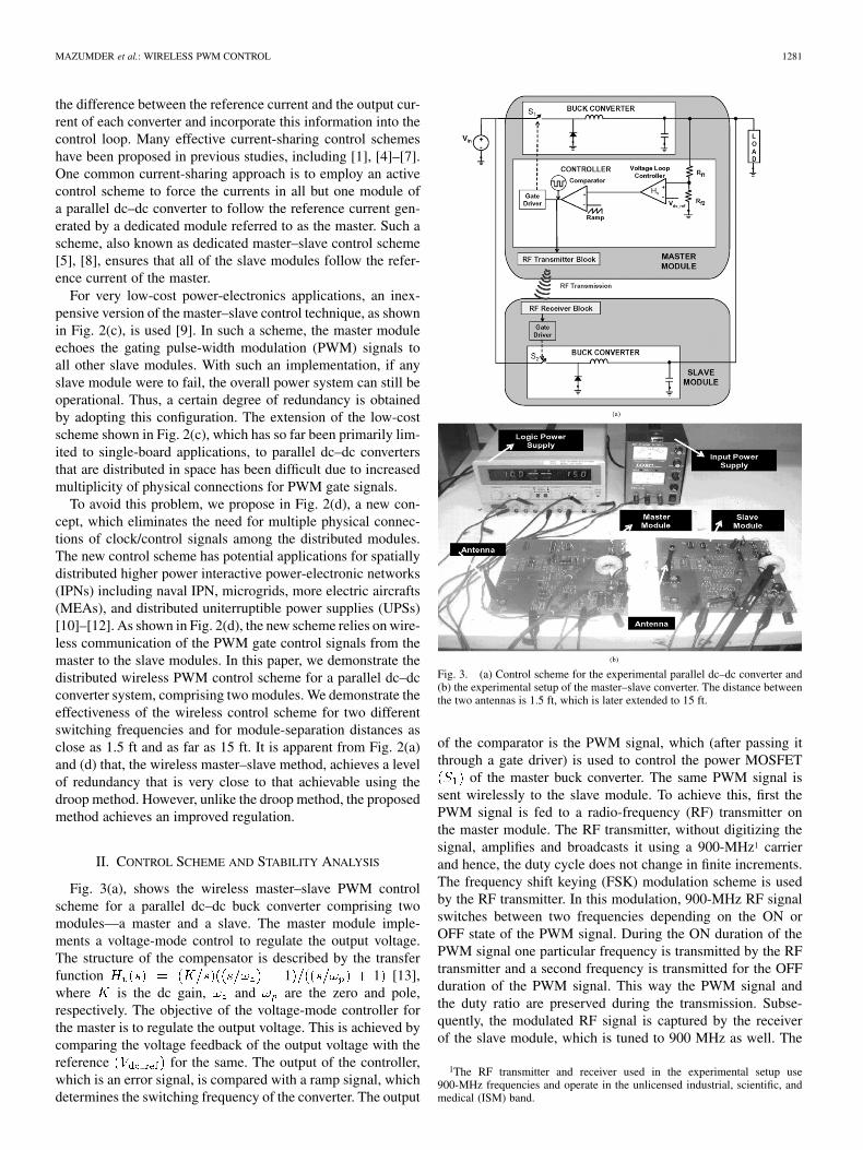
Fig. 3(a), shows the wireless master–slave PWM controlscheme for a parallel dc–dc buck converter comprising twomodules—a master and a slave. The master module imple-ments a voltage-mode control to regulate the output voltage.The structure of the compensator is described by the transferfunction 1 1 [13],where is the dc gain, and are the zero and pole,respectively. The objective of the voltage-mode controller forthe master is to regulate the output voltage. This is achieved bycomparing the voltage feedback of the output voltage with thereference for the same. The output of the controller,which is an error signal, is compared with a ramp signal, whichdetermines the switching frequency of the converter. The output
Fig. 3. (a) Control scheme for the experimental parallel dc–dc converter and(b) the experimental setup of the master–slave converter. The distance betweenthe two antennas is 1.5 ft, which is later extended to 15 ft.
of the comparator is the PWM signal, which (after passing itthrough a gate driver) is used to control the power MOSFET
of the master buck converter. The same PWM signal issent wirelessly to the slave module. To achieve this, first thePWM signal is fed to a radio-frequency (RF) transmitter onthe master module. The RF transmitter, without digitizing thesignal, amplifies and broadcasts it using a 900-MHz1 carrierand hence, the duty cycle does not change in finite increments.The frequency shift keying (FSK) modulation scheme is usedby the RF transmitter. In this modulation, 900-MHz RF signalswitches between two frequencies depending on the ON orOFF state of the PWM signal. During the ON duration of thePWM signal one particular frequency is transmitted by the RFtransmitter and a second frequency is transmitted for the OFFduration of the PWM signal. This way the PWM signal andthe duty ratio are preserved during the transmission. Subse-quently, the modulated RF signal is captured by the receiverof the slave module, which is tuned to 900 MHz as well. The
1The RF transmitter and receiver used in the experimental setup use900-MHz frequencies and operate in the unlicensed industrial, scientific, andmedical (ISM) band.
1282 IEEE TRANSACTIONS ON POWER ELECTRONICS, VOL. 20, NO. 6, NOVEMBER 2005
Fig. 4. Equivalent block diagram for the parallel converter with controller onlyon the master module.
receiver demodulates and amplifies the broadcast signal suchthat the output of the receiver matches the pattern of the originalPWM signal. This signal is then fed to the input of the slavepower-MOSFET gate driver, the output of which controls theMOSFET and thus, ensures equal power sharing betweenthe master and the slave modules. The bandwidth (BW) ofRF transmitter and receiver pair used is 200 Hz–28 kHz andany switching signal within this range can be transmittedusing this pair. The BW requirement for the RF transmissionincreases with the increase in the switching frequency. Thisrequirement can be accomplished by using modules with largertransmission BW, e.g., AR5414 from Atheros. The experi-mental master–slave modules comprising the buck converterand wireless transmitter and receiver are shown in Fig. 3(b).
The equivalent model of the parallel master–slave systemwith voltage controller on the master module while the slavemodule follows the master PWM signal is shown in Fig. 4.
The state space equation for the master–slave power stage isgiven by
(1a)
The state space equivalent of the controller transfer function is
(1b)
where . Combining (1a) with (1b) the statespace realization of the overall system is given by
(1c)
Fig. 5. PWM signal of the master module and the delayed version on theslave module. Simultaneous representation of these two signals determines theswitching pattern S S . Since the slave module follows the signal from themaster module the duty ratio (d) is same on both modules (d = d = d).
where
forforforfor
and
The state vector combines the statesof the voltage mode controller on master module and the statesof master–slave power stages. When the signal is transmittedfrom the master module wirelessly it experiences a delaybefore activating the switch on the slave module. The switchingpatterns of the two switches in one switching cycle are shownin Fig. 5. Below we obtain the steady state solution for the casewhen A similar derivation can be done for the casewhen . For the interval the switching state
is 10 and the system state equation is given by
(2a)
where is the value of at the end of the th switchingcycle. Similarly, the state equations for switching states 11, 01,00, respectively, are
(2b)
(2c)
(2d)
MAZUMDER et al.: WIRELESS PWM CONTROL 1283
Combining the state (2a)–(2d) over one switching cycle we ob-tain
(3)
and the auxiliary equation for the switching condition of theclosed loop feedback system is
(4)
We obtain the equilibrium solution forthe system as
(5)
Solving (4) for duty ratio and substituting in (5) we get equi-librium point solution for the states of the system. Now for smalldisturbances in the states, the duty ratio, the delay, and the inputvoltage we obtain
(6)
and using (6) we linearize the system about the equilibriumpoint to obtain
(7)
(8)
It follows from (8) that
(9)
Using the result from (9) and substituting it in (7) we obtain
where
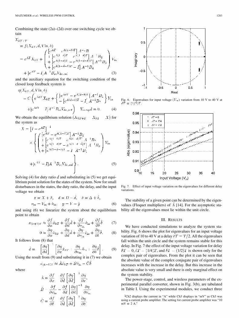
Fig. 6. Eigenvalues for input voltage (V ) variation from 10 V to 40 V atdT = (1=2)T .
Fig. 7. Effect of input voltage variation on the eigenvalues for different delayvariations.
The stability of a given point can be determined by the eigen-values (Floquet multipliers) of [14]. For the asymptotic sta-bility all the eigenvalues must lie within the unit circle.
III. RESULTS
We have conducted simulations to analyze the system sta-bility. Fig. 6 shows the plot for eigenvalues for an input voltagevariation of 10 to 40 V at a delay 2. All the eigenvaluesfall within the unit circle and the system remains stable for thisdelay. In Fig. 7 the effect of the input voltage variation for delay
0 1/4 , and 1/2 is shown only for thecomplex pair of eigenvalues. From the plot it can be seen thatthe absolute value of the complex conjugate pair of eigenvaluesincreases with the increase in the delay. But this increase in theabsolute value is very small and there is only marginal effect onthe system stability.
The power-stage, control, and wireless parameters of the ex-perimental parallel converter, shown in Fig. 3(b), are tabulatedin Table I. Using the experimental modules, we conduct three
2Ch2 displays the current in “A” while Ch3 displays in “mV” as Ch3 wasusing a current probe amplifier. The setting for current probe amplifier was “10mV = 2 A.”
1284 IEEE TRANSACTIONS ON POWER ELECTRONICS, VOL. 20, NO. 6, NOVEMBER 2005
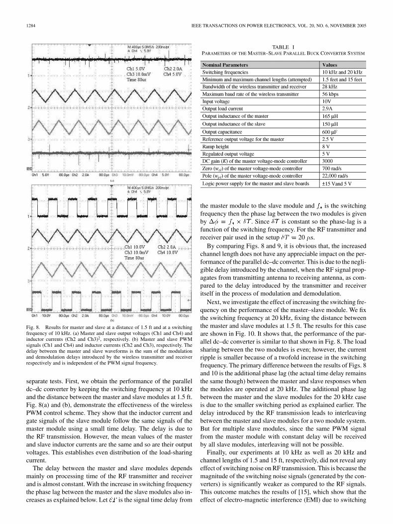
Fig. 8. Results for master and slave at a distance of 1.5 ft and at a switchingfrequency of 10 kHz. (a) Master and slave output voltages (Ch1 and Ch4) andinductor currents (Ch2 and Ch3)2, respectively. (b) Master and slave PWMsignals (Ch1 and Ch4) and inductor currents (Ch2 and Ch3), respectively. Thedelay between the master and slave waveforms is the sum of the modulationand demodulation delays introduced by the wireless transmitter and receiverrespectively and is independent of the PWM signal frequency.
separate tests. First, we obtain the performance of the paralleldc–dc converter by keeping the switching frequency at 10 kHzand the distance between the master and slave modules at 1.5 ft.Fig. 8(a) and (b), demonstrate the effectiveness of the wirelessPWM control scheme. They show that the inductor current andgate signals of the slave module follow the same signals of themaster module using a small time delay. The delay is due tothe RF transmission. However, the mean values of the masterand slave inductor currents are the same and so are their outputvoltages. This establishes even distribution of the load-sharingcurrent.
The delay between the master and slave modules dependsmainly on processing time of the RF transmitter and receiverand is almost constant. With the increase in switching frequencythe phase lag between the master and the slave modules also in-creases as explained below. Let is the signal time delay from
TABLE IPARAMETERS OF THE MASTER–SLAVE PARALLEL BUCK CONVERTER SYSTEM
the master module to the slave module and is the switchingfrequency then the phase lag between the two modules is givenby . Since is constant so the phase-lag is afunction of the switching frequency. For the RF transmitter andreceiver pair used in the setup 20 s.
By comparing Figs. 8 and 9, it is obvious that, the increasedchannel length does not have any appreciable impact on the per-formance of the parallel dc–dc converter. This is due to the negli-gible delay introduced by the channel, when the RF signal prop-agates from transmitting antenna to receiving antenna, as com-pared to the delay introduced by the transmitter and receiveritself in the process of modulation and demodulation.
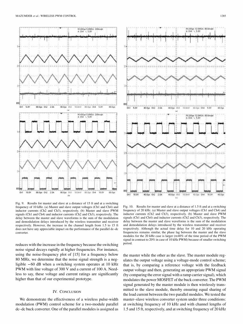
Next, we investigate the effect of increasing the switching fre-quency on the performance of the master–slave module. We fixthe switching frequency at 20 kHz, fixing the distance betweenthe master and slave modules at 1.5 ft. The results for this caseare shown in Fig. 10. It shows that, the performance of the par-allel dc–dc converter is similar to that shown in Fig. 8. The loadsharing between the two modules is even; however, the currentripple is smaller because of a twofold increase in the switchingfrequency. The primary difference between the results of Figs. 8and 10 is the additional phase lag (the actual time delay remainsthe same though) between the master and slave responses whenthe modules are operated at 20 kHz. The additional phase lagbetween the master and the slave modules for the 20 kHz caseis due to the smaller switching period as explained earlier. Thedelay introduced by the RF transmission leads to interleavingbetween the master and slave modules for a two module system.But for multiple slave modules, since the same PWM signalfrom the master module with constant delay will be receivedby all slave modules, interleaving will not be possible.
Finally, our experiments at 10 kHz as well as 20 kHz andchannel lengths of 1.5 and 15 ft, respectively, did not reveal anyeffect of switching noise on RF transmission. This is because themagnitude of the switching noise signals (generated by the con-verters) is significantly weaker as compared to the RF signals.This outcome matches the results of [15], which show that theeffect of electro-magnetic interference (EMI) due to switching
MAZUMDER et al.: WIRELESS PWM CONTROL 1285
Fig. 9. Results for master and slave at a distance of 15 ft and at a switchingfrequency of 10 kHz. (a) Master and slave output voltages (Ch1 and Ch4) andinductor currents (Ch2 and Ch3), respectively. (b) Master and slave PWMsignals (Ch1 and Ch4) and inductor currents (Ch2 and Ch3), respectively. Thedelay between the master and slave waveforms is the sum of the modulationand demodulation delays introduced by the wireless transmitter and receiverrespectively. However, the increase in the channel length from 1.5 to 15 ftdoes not have any appreciable impact on the performance of the parallel dc–dcconverter.
reduces with the increase in the frequency because the switchingnoise signal decays rapidly at higher frequencies. For instance,using the noise-frequency plot of [15] for a frequency below80 MHz, we determine that the noise signal strength is a neg-ligible 60 dB when a switching system operates at 10 kHzPWM with line voltage of 300 V and a current of 100 A. Need-less to say, these voltage and current ratings are significantlyhigher than that of our experimental prototype.
IV. CONCLUSION
We demonstrate the effectiveness of a wireless pulse-widthmodulation (PWM) control scheme for a two-module paralleldc–dc buck converter. One of the parallel modules is assigned as
Fig. 10. Results for master and slave at a distance of 1.5 ft and at a switchingfrequency of 20 kHz. (a) Master and slave output voltages (Ch1 and Ch4) andinductor currents (Ch2 and Ch3), respectively. (b) Master and slave PWMsignals (Ch1 and Ch4) and inductor currents (Ch2 and Ch3), respectively. Thedelay between the master and slave waveforms is the sum of the modulationand demodulation delays introduced by the wireless transmitter and receiverrespectively. Although the actual time delay for 10 and 20 kHz operatingfrequencies remains similar, the phase lag between the master and the slavemodules for the 20 kHz case is larger (�40% of the time period of the PWMsignal in contrast to 20% in case of 10 kHz PWM) because of smaller switchingperiod.
the master while the other as the slave. The master module reg-ulates the output voltage using a voltage-mode control scheme;that is, by comparing a reference voltage with the feedbackoutput voltage and then, generating an appropriate PWM signal(by comparing the error signal with a ramp carrier signal), whichmodulates the power MOSFET of the buck converter. The PWMsignal generated by the master module is then wirelessly trans-mitted to the slave module, thereby ensuring equal sharing ofthe load current between the two parallel modules. We tested themaster–slave wireless converter system under three conditions:at switching frequency of 10 kHz and with channel lengths of1.5 and 15 ft, respectively, and at switching frequency of 20 kHz
1286 IEEE TRANSACTIONS ON POWER ELECTRONICS, VOL. 20, NO. 6, NOVEMBER 2005
for a channel length of 1.5 ft. The averaged load current sharingfor all the three cases was even. A delay was observed betweenthe master and slave responses, which is attributed to the pro-cessing limitation of the wireless transmitter and receiver mod-ules. The effect of this delay on the stability of parallel convertersystem is studied. From the analysis it is clear that the effect ofthe delay on the system stability is marginal for delays boundedby half switching cycle.
Although this delay is fixed, it translates to a greater phaseshift between the master and slave inductor currents at 20 kHzthan that at 10 kHz because of the smaller time period of theformer. Finally, we observed that, for the wireless transmitter,which has a range of 90 feet, increase in the channel lengthfrom 1.5 ft to 15 ft has no appreciable effect at 10 kHz. Thenew concept for controlling a parallel dc–dc converter, proposedin this paper, eliminates the need for multiple wire connectionsof PWM/gate signals among the distributed modules and hasapplicability for multiple parallel converter topologies. We haveextended this concept to dc–ac converters and have applied it toa two-module parallel voltage source inverter (VSI) [12].
The choice of the RF transmitter and receiver pair is dictatedby, the switching frequency of the system, number of parallelmodules, selection between bandwidth and cost and the spa-tial distribution of the modules. Also at very high switchingfrequencies the delay introduced by the RF transmitter and re-ceiver becomes significant and this issue should be addressed indesigning the RF interface. One solution can be an ASIC inte-grating both the control and RF interface on the same chip andhence reducing the delay due to processing on the transmitterand receiver modules.
ACKNOWLEDGMENT
The authors would like to thank reviewers for their construc-tive comments.
REFERENCES
[1] M. Jordan, “UC3907 load share IC simplifies parallel power supply de-sign,” Application Note U-129, Unitrode, 1991–1996.
[2] D. Perreault, R. Selders, and J. Kassakian, “Frequency-based current-sharing techniques for paralleled converters,” in Proc. IEEE PESC’96,1996, pp. 1073–1079.
[3] C. Jamerson and C. Mullett, “Parallel supplies via various droopmethods,” in Proc. High Frequency Power Conversion Conf., 1994, pp.68–76.
[4] K. Siri and C. Q. Lee, “Current distributed control of convertersconnected in parallel,” in Proc. IEEE Industry Applications Soc. Conf.,1990, pp. 1274–1280.
[5] K. Siri, “Analysis and Design of Distributed Power Systems,” Ph.D. dis-sertation, Dept. Elect. Eng., Univ. Illinois, Chicago, IL, 1991.
[6] S. K. Mazumder, A. H. Nayfeh, and D. Boroyevich, “Robust control ofparallel dc–dc buck converters by combining integral-variable-structureand multiple-sliding-surface control schemes,” IEEE Trans. Power Elec-tron., vol. 17, no. 3, pp. 428–437, May 2002.
[7] V. J. Thottuvelil and G. C. Verghese, “Stability analysis of parallelDC/DC converters with active current sharing,” in Proc. IEEE PESC’96,1996, pp. 1080–1086.
[8] K. Xing, S. K. Mazumder, Z. Ye, F. C. Lee, and D. Boroyevich, “The cir-culating current in paralleled three-phase boost PFC rectifiers,” in Proc.IEEE PESC’98, 1998, pp. 783–789.
[9] F. Petruzziello, P. D. Ziogas, and G. Joos, “A novel approach to par-alleling of power converter units with true redundancy,” in Proc. IEEEPESC’90, 1990, pp. 808–813.
[10] G. S. Thandi, “Modeling, Control and Stability Analysis of a PEBBBased dc Distribution Power System,” Ph.D. dissertation, Dept. Elect.Eng., Virginia Polytech. Inst. State Univ., Blacksburg, VA, 1997.
[11] R. H. Lasseter, “Microgrids,” in Proc. IEEE Power Engineering Soc.Winter Meeting, 2002, pp. 305–308.
[12] S. K. Mazumder, K. Acharya, and M. Tahir, “Wireless control of spa-tially distributed power electronics,” in Proc. 20th Annu. IEEE AppliedPower Electronics Conf. Expo, vol. 1, Mar. 2005, pp. 75–81.
[13] F. C. Lee, Modeling, Analysis, and Design of PWM Con-verters. Blacksburg, VA: Virginia Power Electronic Center, 1990,vol. 2.
[14] S. K. Mazumder, A. H. Nayfeh, and D. Boroyevich, “Theoretical andexperimental investigation of the fast- and slow-scale instabilities ofa dc–dc converter,” IEEE Trans. Power Electron., vol. 16, no. 2, pp.201–216, Mar. 2001.
[15] C. Chen, “Characterization of power electronics EMI emission,” inProc. IEEE Int. Symp. Electromagnetic Compatibility, vol. 2, 2003, pp.553–557.
Sudip K. Mazumder (SM’02) is the Director of theLaboratory for Energy and Switching-ElectronicsSystems (LESES) and an Assistant Professor in theDepartment of Electrical and Computer Engineering,University of Illinois, Chicago. He has over 10 yearsof professional experience and has held R&D anddesign positions in leading industrial organizations.He has published over 50 refereed and invitedjournal and conference papers and is a reviewer for 6International Journals. His current areas of interestsare interactive power-electronics/power networks,
renewable and alternate energy systems, and new device and systems-on-chipenabled higher power density.
Dr. Mazumder received the IEEE PELS Award in 2002, the DOE SECAAward in 2002, the NSF CAREER Award in 2003, the Prize Paper Award fromthe IEEE TRANSACTIONS ON POWER ELECTRONICS, and the the ONR Young In-vestigator Award in 2005. He is an Associate Editor for the IEEE TRANSACTIONS
ON INDUSTRIAL ELECTRONICS and the IEEE POWER ELECTRONICS LETTERS.
Muhammad Tahir (S’03) received the B.Sc. degreein electrical engineering and the M.Sc. degree incomputer engineering from the University of Engi-neering and Technology Lahore, Lahore, Pakistan,in 1999 and 2003, respectively, and is currentlypursuing the Ph.D. degree at the Laboratory for En-ergy and Switching-Electronics Systems (LESES),Department of Electrical and Computer Engineering,University of Illinois, Chicago.
From 2000 to 2003, he was a Lecturer in theElectrical Engineering Department, University of
Engineering and Technology Lahore and an Embedded System Engineer withMentor Graphics Pakistan. His research interests include distributed wirelesscontrol of high frequency switching systems and analysis of time delay systems.
Srividya Lavanya Kamisetty (S’03) received theB.E. degree in electrical and computer engineeringfrom Osmania University, Hyderabad, India, in 2001and the M.S. degree in electrical engineering fromthe University of Illinois, Chicago, in 2003.
She joined Servo Tech. Inc., Chicago, in 2004. Herresearch interests include design of voltage regulatormodules, nonlinear controls, and dc/dc converter de-sign.