Stability analysis of a single inductor dual switching dc-dc converter
Upload
independentCategory
view
0download
0
HIGH FREQUENCY INVERTER
Thesis
Submitted by
Karuna Mudliyar
Reg No. 110943004
Under the guidance of
SURYANARAYANA K
&
H.V. GURURAJ RAO
In partial fulfilment of the requirements for the award of the degree of
MASTER OF TECHNOLOGY
In
POWER ELECTRONIC SYSTEMS AND CONTROL
DEPARTMENT OF ELECTRICAL AND ELECTRONICS ENGINEERING
MANIPAL INSTITUTE OF TECHNOLOGY (A Constituent College of Manipal University)
MANIPAL – 576104, KARNATAKA, INDIA

To My Parents
Gowri and GnanaPrakasam

DEPARTMENT OF ELECTRICAL AND ELECTRONICS ENGINEERING
MANIPAL INSTITUTE OF TECHNOLOGY
(A Constituent College of Manipal University)
MANIPAL – 576 104 (KARNATAKA), INDIA
Manipal
20/5/2013
CERTIFICATE
This is to certify that the project titled “HIGH FREQUENCY INVERTER” is a record
of the bona-fide work done by KARUNA MUDLIYAR (Reg No. 110943004) submitted
in partial fulfilment of the requirements for the award of the Degree of Master of
Technology (M.Tech) in POWER ELECTRONIC SYSTEMS AND CONTROL of
Manipal Institute of Technology Manipal, Karnataka, (A Constituent College of Manipal
University), during the academic year 2012-13.
H.V. Gururaj Rao Dr.B.K.Singh
Project guide HOD, E&E
Asst.Professor (Sel. Grade) MIT, MANIPAL
MIT, MANIPAL

(On Company Letterhead)
Mysore
20/2013
CERTIFICATE
This is to certify that the project entitled HIGH FREQUENCY INVERTER was
carried out by KARUNA MUDLIYAR (Reg. No. 110943004) at HEXMOTO
CONTROLS Pvt. Ltd, Mysore under my guidance during JUNE to APRIL 2013.
--------------------------------------------
SURYANARAYANA K
Manager,
Hexmoto Controls Pvt Ltd.
Mysore
--------------------------------------------
L V Prabhu
Director,
Hexmoto Controls Pvt Ltd.
Mysore

iii
ACKNOWLEDGMENTS
I would like to thank first and foremost my advisors, H.V.Gururaj Rao and Suryanarayana
K for their kind guidance and help at Manipal Institute of Technology and Hexmoto
Controls Pvt Ltd respectively, without whom my research and this thesis would not have
been possible. I still can remember how they reviewed my work, which opened my mind to
the real field of power electronics. He is always generous to give me suggestions,
encouragement and ideas to help me dig into some unknown areas. His dedication and
earnest work attitude gave me courage when I met problems. In particular, I am very
grateful to the director of MIT Dr. V.V.Thomas and HOD of Electrical and Electronics
Department Dr. B.K Singh for their support. I also wish to thank Mr. L V Prabhu and Mr.
Krishna Prasad, directors of Hexmoto Controls Pvt Ltd, for there incisive view and vast
experience on power electronics. They guided me in the right research area which saved
lots of my time. Mr Suryanarayana’s guidance on technical writing and research habits is
highly valuable to me and for my future work.
For their support and direction over years, I would like to express my heartfelt
gratitude to the entire faculty member of the Electrical and Electronics department at
Manipal Institute of Technology. Their classes and innovative work has given me
inspiration and sparked my interest in the area of power electronics. I would also thank my
fellow Hexmoto friends and colleagues, Viswash K, Chetan Midha, always helping me
whenever I am in doubt; their suggestion helped me a lot and saved much of time.
I am especially indebted to my friends Adarsh Srinivasan and Mohammed Haseeb
for their help throughout my M.Tech Course. I also would like to give a special mention
and thanks to my friends in MIT hostel Vipin, Anoop and Ankit for making my stay
enjoyable and my fellow classmates and friends in M.Tech electrical department for
barring my very casual attitude and I always cherish those memories. Finally I would like
to thank everyone in R & D and Production Department at Hexmoto for their help,
suggestions, and friendship throughout my time and for all the great memories away from
the research.
Last but not least, with deepest love, I dedicate my appreciation to my Parents, who
has always been there with love, support, understanding and encouragement for all my
endeavours. Although far away from Bombay, they always concentrate on my life here and
gave me great support and encouragement. I can feel their selfless love all the time. Your
love and encouragement has been the most valuable thing in my life!

iv
ABSTRACT
A novel approach to achieve a high static gain in non-isolated dc-dc converter is presented
in this thesis. The conventional boost converter is cascaded to step-up the voltage to higher
level and the initial few stages are multi-phased to avoid high input current stress on the
switch. The Multi-phase booster configuration can reduce significantly the resultant
inductor current ripple and the voltage ripple due to the operation of the parallel stages
with relative phases, thereby reducing the filter size. The operational principle and the
design procedure are presented for Multi-Phase, Multi-Stage and integrated Multi-Phase
Multi-Stage boost converter. The main application of Multi-Phase Multi-Stage booster is
pointed to be in battery sourced Inverter design, where it replaces the step – up
transformer.
With the growth of battery powered application, there is a huge demand of highly
efficient, small size, low cost and high step up dc-dc converter. Typical applications are
hybrid vehicle, uninterrupted power supply and renewable energy system such as solar.
The step-up stage normally is the critical point for the design of high efficiency converters
due to the operation with high input current and high output voltage, thus a detailed study
is carried out, in order to define the topology for a high step-up application.
Magnetic coupled classic converter such as flyback or push-pull converter can be
used to achieve high static gain. However, volume of power transformer will greatly
influence the size of converter. The leakage inductance can produce voltage stress; high
switching frequency will bring down the efficiency of the transformer itself and will cause
electromagnetic Interference (EMI), thereby reducing the converter’s efficiency. Non-
isolated conventional boost converter, can provide high step-up voltage gain but with the
penalty of high voltage and current stress on semiconductor switches, high duty cycle
operation.
This thesis also includes steady – state analysis, small – signal ac modeling and
closed loop control of Multi-Stage Multi-Phase boost converter with Type III compensator
employed. All the analysis, modeling and design variables are derived considering the
converter’s parasitic effects such as copper loss and semiconductor losses. The interleaved
switching sequence is discussed for three-phase boost converter. The charging operation of
High frequency Inverter in discussed where the Inverter operates as rectifier and booster in
buck mode. The designed Multi-Phase Multi-Stage booster is verified with Mat-
Lab/Simulink.
Thus, the new boost configuration paves the way, to have efficient high voltage
step – up gain, with simpler structure. Due to multi-phasing and interleaved switching
sequence the effective pulse frequency increases and the magnitude of resultant ripple
reduces thus leading to a small filter size. As a whole a compact and efficient booster
configuration is attained.

v
List of Tables
Table 1: Multi-Phase Multi-Stage Booster design specifications ............................................... 16
Table 2: Power Stage specifications for stage II and III ............................................................. 35
Table 3: Switch position for different states ................................................................................ 39

vi
List of Figures
Figure 1-1: High Frequency Link Inverter .................................................................................... 2
Figure 1-2 Boost Converter with Voltage Doubler Circuit .......................................................... 4
Figure 1-3: Multi-Stage Boost Converter with single switch........................................................ 5
Figure 1-4: Multi Stage Boost Converter ....................................................................................... 6
Figure 1-5: Multi-Phase Boost Converter ...................................................................................... 6
Figure 1-6: Multi-Phase Multi-Stage Booster ................................................................................ 7
Figure 2-1: Three Stage Boost Converter ...................................................................................... 9
Figure 2-2 Sub - Interval I: (a) reduced linear circuit, (b) pulse modulation ........................... 10
Figure 2-3: Sub-Interval 2: (a) reduced linear circuit, (b) pulse modulation ........................... 11
Figure 2-4: Three Phase Boost Converter .................................................................................... 13
Figure 2-5: Interleaved Waveform ............................................................................................... 14
Figure 2-6: Simulink Model - Three Phase Three Stage Booster .............................................. 20
Figure 2-7: Stage I Three Phase Inductor currents .................................................................... 21
Figure 2-8: Interleaved Three Phase Inductor currents ............................................................. 21
Figure 2-9: Stage II and Stage III Inductor currents .................................................................. 22
Figure 2-10: Three Stage Output Voltages .................................................................................. 22
Figure 3-1: Voltage Mode Controlled Boost Converter .............................................................. 27
Figure 3-2: Sub-Interval I.............................................................................................................. 28
Figure 3-3: Sub-Interval II ............................................................................................................ 29
Figure 3-4: TYPE III Compensator ............................................................................................. 33
Figure 3-5: Stage II control-to-output transfer function ............................................................ 35
Figure 3-6: Stage II Compensated Bode plot ............................................................................... 36
Figure 3-7: Stage II Uncompensated bode plot ........................................................................... 36
Figure 3-8: Stage III compensated system ................................................................................... 37
Figure 3-9: Three-Phase Boost Converter ................................................................................... 38
Figure 3-10: Interleaved Switching Gate Pulse ........................................................................... 39
Figure 3-11: State I II III ............................................................................................................... 40
Figure 3-12: State II ....................................................................................................................... 41
Figure 3-13: State IV ...................................................................................................................... 42
Figure 3-14: State VI ...................................................................................................................... 43
Figure 3-15: Stage I - Uncompensated bode plot......................................................................... 46
Figure 3-16: Stage I Compensated system ................................................................................... 47
Figure 4-1: Power Loss compared with synchronous switching ................................................ 49

vii
Contents
Acknowledgement………………………………………………………………………………....iii
Abstract…………………………………………………………………………….........................iv
List of Tables…………………………………………………………………………………….....v
List of Figures………………………………………………………………………………….......vi
1 INTRODUCTION ..................................................................................................................... 1
1.1 BACKGROUND THEORY – DC TO AC CONVERSION ............................................. 1
1.2 MOTIVATION .................................................................................................................. 1
1.3 HIGH FREQUENCY LINK INVERTER .......................................................................... 2
1.3.1 HF LINK INVERTER - SHORTCOMINGS ................................................................. 3
1.4 BOOSTER DESIGN .......................................................................................................... 4
1.4.1 BOOST CONVERTER WITH VOLTAGE MULTIPLIER CELL ............................... 4
1.4.2 MULTI-STAGE BOOST CONVERTER ...................................................................... 5
1.4.3 MULTI-PHASE BOOST CONVERTER ...................................................................... 6
1.5 MULTI-PHASE MULTI-STAGE BOOST CONVERTER .............................................. 7
1.6 HIGH FREQUENCY INVERTER .................................................................................... 7
1.7 OBJECTIVE OF WORK ................................................................................................... 8
1.8 OUTLINE OF THESIS ...................................................................................................... 8
2 BACKGROUND THEORY ..................................................................................................... 9
2.1 THREE-STAGE BOOST CONVERTER .......................................................................... 9
2.1.1 STEADY – STATE ANALYSIS OF THREE STAGE BOOSTER ............................ 10
2.2 THREE – PHASE BOOST CONVERTER ..................................................................... 13
2.2.1 INTERLEAVING ........................................................................................................ 14
2.2.2 STEADY STATE ANALYSIS OF THE THREE-PHASE BOOSTER ...................... 15
2.3 DESIGN – MULTI-PHASE MULTI-STAGE BOOSTER .............................................. 16
2.3.1 STATIC GAIN ............................................................................................................. 17
2.3.2 EQUIVALENT LOAD AT EACH STAGE ................................................................ 17
2.3.3 INDUCTANCE AND CAPACITANCE ..................................................................... 18
2.4 SIMULATION VERIFICATION OF MULTI-PHASE MULTI-STAGE DESIGN ....... 20
2.5 BATTERY CHARGING MODE OF HIGH FREQUENCY INVERTER ...................... 23
2.5.1 MAT-LAB SIMULATION – CHARGING MODE. ................................................... 23
2.5.2 BATTERY CHARGING VOLTAGE AND CURRENT ............................................ 24
3 METHODOLOGY ................................................................................................................. 27
3.1 INTRODUCTION – MODELING AND CONTROL ..................................................... 27

viii
3.2 SMALL SIGNAL AC MODELING OF BOOST CONVERTER ................................... 28
3.2.1 SUB-INTERVAL I ...................................................................................................... 28
3.2.2 SUB-INTERVAL II ..................................................................................................... 29
3.3 RIGHT HALF PLANE ZERO IN BOOST CONVERTER ............................................. 33
3.4 COMPENSATION FOR VOLTAGE MODE BOOST CONVERTER .......................... 33
3.4.1 TYPE III COMPENSATOR ........................................................................................ 33
3.4.2 BOOST CONVERTER VOLTAGE MODE CHARACTERISTICS .......................... 34
3.5 CLOSED LOOP CONTROL – STAGE II AND STAGE III .......................................... 34
3.6 MULTI-PHASE BOOST CONVERTER MODELING .................................................. 38
3.6.1 MODELLING OF THREE-PHASE BOOST CONVERTER ..................................... 38
3.6.2 INTERLEAVED SWITCHING SEQUENCE ............................................................. 38
3.6.3 STATE I III V .............................................................................................................. 39
3.6.4 STATE II ...................................................................................................................... 41
3.6.5 STATE IV .................................................................................................................... 42
3.6.6 STATE VI .................................................................................................................... 43
3.6.7 AVERAGING – STATE MATRIX OF THREE PHASE BOOSTER ........................ 44
3.7 CLOSED LOOP CONTROL – MULTI-PHASE BOOST CONVERTER ..................... 46
4 RESULT ANALYSIS ............................................................................................................. 48
4.1 TRANSIENT RESPONSE ............................................................................................... 48
4.2 SYNCHRONOUS SWITCHING .................................................................................... 48
4.3 FREQUENCY RESPONSE ............................................................................................. 49
4.4 HARDWARE DESIGN BASED ON SIMULATION RESULTS .................................. 50
5 CONCLUSIONS & FUTURE SCOPE OF WORK ............................................................. 51
5.1 WORK CONCLUSION ................................................................................................... 51
5.2 FUTURE SCOPE OF WORK .......................................................................................... 52
REFERENCES ............................................................................................................................... 53

Introduction
1
1 INTRODUCTION
This thesis is concerned with the steady state analysis, small signal ac modeling and
close loop control of Multi-Phase and Multi-Stage Boost converters. The objective of
the work is to integrate Multi-Phase Multi-Stage booster with SPWM Inverter in
order to build a High Frequency Inverter system which outputs a 230 VAC sourced
from a 12 VDC battery.
In this chapter, the background of the problem is discussed, the motivation for
the work is presented and the contributions of the thesis are outlined. This chapter
introduces to the area of work on DC-AC conversion and the present day scenario of
existing Inverter. It also points out the shortcoming of the previous work and
discusses the uniqueness of the methodology that will be adopted in this thesis. The
literature review and its outcome are summarized in the further sections of this
chapter. The main objective of the work is framed and target is specified.
1.1 BACKGROUND THEORY – DC TO AC CONVERSION
Switch-mode single-phase DC-AC inverters have been widely used in many
applications such as AC motor drives, uninterrupted power supply systems, induction
heating and renewable energy source systems.
The simplest form of an inverter is the bridge-type [3], where a power bridge
is controlled by sinusoidal pulse-width modulation1 (SPWM) principle and the
resulting SPWM wave is filtered to produce the alternating output voltage. This
method have disadvantage that in the case where low direct input voltage is used, the
power transformer required is of large size, heavy weight and high cost [3]. In
addition most of the Inverters are sourced by battery, so the converters should be
highly efficient to optimally use the available resource. This thesis figures out the
design technique to attain small size, highly efficient and light weight Inverters.
1.2 MOTIVATION
In recent years, many places in the world have been experiencing continued shortage
of electric power or energy crisis due to their fast increasing demand. To solve this
problem, significant efforts of research and development have been given in two
areas: Firstly, develop efficient renewable energy generation and conversion systems
to supplement conventional fossil-fuel based energy supply and eventually replace it.
Secondly, improve the efficiency of present power conversion and utilization system.
This is possible with the use of appropriate power semiconductor devices and
converters. Various high power semiconductor devices, such as Isolated Gate Bipolar
Transistors (IGBT) and power MOSFET were developed and become commercially
1 Using SPWM, desired output voltage is achieved by comparing the desired reference waveform
(modulating signal) with a high-frequency triangular wave (carrier).

Introduction
2
available. Nowadays, the increased power ratings as well as switching speed; ease of
control and reduced costs of power semiconductor devices make the new converter
topologies possible. The renewable energy generation and conversion (REGC)
system has many advantages over conventional energy supply, e.g. the ability of
regeneration, re-usability and less pollution. However, the renewable energy
generation and conversion technologies are not completely mature yet. There still
exist problems such as low efficiency and high cost. The main sources of renewable
energy currently under development include solar, wind, hydro-power and biomass,
etc. The solar power system has the potential to become one of the main renewable
energy sources due to the commercial availability of semiconductor based
photovoltaic devices, reduction in the system cost and development of power
electronic technologies and thus in recent years, the solar power generation and
conversion technology is developing rapidly [9]. This solar power is stored in a
battery banks to make available to the external load. The important tasks is to make
solar power generation and conversion system more efficient and more reliable. One
of the main objectives of this thesis is to evaluate and improve the system
configuration and circuit topologies of power conversion system.
1.3 HIGH FREQUENCY LINK INVERTER
Many present applications use the bridge inverter to convert the direct input voltage
into a High frequency square wave, which, in turn, is filtered and stepped – up with
the help of transformer to boost the voltage to higher level [3]. One such type of
application is a high frequency Link Inverter.
In many applications it is important for an inverter to be of relatively small size and
lightweight. It achieved by using a high-frequency link inverter topology also a
popular HF link inverter topology is the so-called DC/DC converter type [3], as
shown in Figure 1-1.
S12
S11 S13
S14
D1
D2 D4
D3S21
S22
S23
S24
L
O
A
DT
HIGH FREQUENCY
INVERTER
HIGH FREQUENCY
TRANSFORMER
DIODE BRIDGE
RECTIFIER
SPWM
INVERTERFILTER
L
CVin
Figure 1-1: High Frequency Link Inverter
Introduction
3
It uses a bridge inverter to convert the direct input voltage into an HF square wave,
which, in turn, is rectified and filtered. The low pass filter output is a high-level
direct voltage that is converted into a low-frequency wave by a Sine-wave Pulse
width modulation inverter. It is a three level converter. At first level the DC battery
voltage is converted to a high frequency AC voltage i.e. Inversion, then AC voltage
is boosted to higher voltage level by using a high frequency inverter i.e. Boosting.
The high level AC voltage is converted to DC by a bridge rectifier at second level
i.e. Rectification. At final level this DC voltage is converted to 50 Hz AC voltage
using Sinusoidal pulse width modulator. With use of high frequency inverter at first
stage, the transformer size will get smaller [3]. As we know, voltage across the
winding is number of coil times the change in flux linkage with respect to time.
(1.1)
1.3.1 HF LINK INVERTER - SHORTCOMINGS
Higher the frequency, less number of windings are required in transformer. Thus the
switching frequency of the inverter should be very high, so the transformer size can
be brought down considerably, and the size and weight of the inverter can be
reduced. Here, high frequency transformer is involved in the design topology, based
on the design rating the transformer need to be customized. It is known that, if the
Inverter is switched at higher frequency, the number of transformer winding required
would be very less for boosting the voltage to high level. In addition, the size of the
filter required will be very small. But, if the semiconductor devices are allowed to
switch at very high frequency, it tends lossy to the system. The modern Power
electronics semiconductor devices such as IGBT and MOSFET are capable for
switching at very high frequency. They can withstand large voltage and can allow
large current through it. Due to non-idealist of the practical Semiconductor device,
the transition of the device is not instantaneous. The turn ON and turn OFF of the
switch lasts for finite amount of time, during which the voltage across and the
current through the switch is high, thus leading to the power loss during switching
[5]. During each period of the cycle, apart from the conduction loss, there is
switching loss and switching loss increases with the increasing frequency. Every
practical switching device has a limit on the switching frequency, and this limit is
determined by the turn-on and turn-off time of the device. Another significant
drawback of the high frequency switching is the EMI produced due to the large
and . These shortcomings can be avoided if the device is subjected to change
its status form on-to-off or vice-versa when the current through it or the voltage
across it is zero [17]. Thus, the converter topologies and the switching strategies,
which results in zero-voltage and/or zero-current (Resonant Converters) switching
should be adopted for an efficient system. The resonant converter will work fine for

Introduction
4
a given load, but not for wide range of load. The load voltage can be regulated by
having a frequency modulation which is difficult to design and implement.
1.4 BOOSTER DESIGN
The step-up stage normally is the critical point for the design of high efficiency
converters due to the operation with high input current and high output voltage, thus
a careful study is required in order to define the topology for a high step-up
application [8]. From the section 1.3, with High Frequency Link Inverter, to reduce
size and weight of the transformer the switching frequency of the converter was
increased, but it ended with switching losses and the design of a customized highly
efficient transformer is too difficult [3]. To avoid switching losses, resonant
converter2 and the DC Link inverter topology were chosen, but it too ended with
inefficiency in implementation. Thus, there is need for an alternate booster, which
doesn’t incorporate transformer as boosting component. As per the thumb rule used
for the design of conventional boost converter, the voltage cannot be stepped up
more than four times the input voltage, i.e. the maximum duty ratio allowed is 0.75.
For very high static gain in conventional boost converter, the switch is stressed by
very high input current during ON period of switching cycle and very high output
during OFF condition. The booster should be of small size, highly efficient, and be
easy in control on load variations.
1.4.1 BOOST CONVERTER WITH VOLTAGE MULTIPLIER CELL
The conventional boost converter is used along with voltage multiplier circuit to
step up the voltage to a very higher level [2]. The Figure 1-2 below shows a boost
converter cascaded with the voltage multiplier cell. For very high static gain many
such voltage multipliers can be cascaded. The basic concept is to use a voltage
doubler circuit composed of diodes and capacitor, as one multiplier cell.
SCM12 CM22
L
DM11 DM12
CM11 CM21
DM22DM21
CMn1
DMn1 DMn2
CMn2
Do
Co RVin
Figure 1-2 Boost Converter with Voltage Doubler Circuit
2 Resonant converters use a resonant circuit for switching the transistors when they are at the zero current or
zero voltage point; this reduces the stress on the switching transistors and the radio interference.

Introduction
5
For a boost converter, composed of M cascaded voltage multiplier circuit, the
output voltage will be multiplied by the factor (M + 1). Thus the static gain of the
proposed converter is given by,
(1.2)
Where, M – number of voltage multiplier cells
D - Duty cycle
the nominal duty cycle is defined by,
(1.3)
Considering the project, the first stage booster has to boost the voltage from 12V
battery to around 380V to 400V. It results the static gain of 32 and the max duty
ratio allowed as per thumb rule is 0.75. Thus, the number of voltage multiplier
stages required is 8. It does not replicate a good design to have boost converter with
8 voltage multiplier stages. For the inverter used in On-line UPS, the settling time
is very critical but the inverter incorporating boost converter with voltage multiplier
cell takes more time to settle to its final voltage level.
1.4.2 MULTI-STAGE BOOST CONVERTER
It is a novel approach where a cascaded boost converter results in the output
voltage increasing in a geometric progression that to with a simple structure [10].
The Figure 1-3 shows a three stage boost converter.
L1 L2
L3
D1
D2
C1 C2
D3
D4
D5
C3
RS
Stage 1 Stage2 Stage3
Vin
Figure 1-3: Multi-Stage Boost Converter with single switch
This converter topology suits much better for boosting the voltage from 12V
battery to around 380V with the duty ratio of less than 0.7. In the case with high
step- up static gain, as the voltage level is raised to higher level correspondingly the

Introduction
6
input current too raises to a high level, power equality [11]. Thus, with the Multi-
stage Boost converter discussed, the high input current has to flow through the
switch S and it proves to be stress on it. So a slight variation in the converter can be
made by replacing the diode D2 and D4 with switch S1 and S2 and connecting to
the ground as shown in the Figure 1-4 below.
L1 D1
C1
L2 D2 Ln
C2
Dn
Cn R
Stage 1 Stage2 Stage3
S1 S2 SnVin
Figure 1-4: Multi Stage Boost Converter
This booster topology proves to best for high step up voltage, but at the same time
it also posses high input current stress on the initial stage switches and Inductors.
Thus the current at the initial stages need to be shared.
1.4.3 MULTI-PHASE BOOST CONVERTER
To avoid high current stress on the switch and inductor of the boost converter, the
conventional boost converter can be multi phased, thus higher efficiency is ensured
[1], [7]. The multi-phase booster can be achieved by adding more parallel legs to
the conventional boost converter [28], [29]. The Figure 1-5 below shows a three-
phase boost converter, where two more legs are connected in parallel with the
conventional one. A suitable algorithm is required for control switches to achieve
the interleaved switching sequence [6].
L1
L2
Ln
D1
C
R
S1 S2 SnVin
D2
Dn
Figure 1-5: Multi-Phase Boost Converter

Introduction
7
Because of the phase difference in the multi-phasing the inductor ripple currents
tend to cancel each other, resulting in a smaller ripple current with increased
frequency flowing into the output capacitor [9]. The output voltage will be same as
that of the conventional converter, but the input inductor current will be reduced by
the number of phases.
(1.4)
Where = Number of Phase,
Multi-phase converters reduce the input and output ripple currents by interleaving
the gate pulse for paralleled power stages. With a proper choice of phase number,
the output ripple voltage and the input capacitor size can be minimized without
increasing the switching frequency.
1.5 MULTI-PHASE MULTI-STAGE BOOST CONVERTER
By combining the advantages of the Multi-Stage and Multi-Phase Boost converter, a
novel topology is structured called Multi-Phase Multi-Stage Boost converter , as
shown in Figure 1-6. Thus, high current at the initial stage is shared due to multi-
phase and the high static step-up gain is achieved due to multi-stage.
L11
L1n
S11 S12 S1n
D11
D12
D1n
C1
L12
Vin
L21
L22
L2n
S21 S22 S2n
D21
D22
D2n
C2
Ln1
Ln2
Lnn
Sn1 Sn2 Snn
Dn1
Dn2
Dnn
Cn
R
Figure 1-6: Multi-Phase Multi-Stage Booster
1.6 HIGH FREQUENCY INVERTER
The Multi-Phase Multi-Stage Booster is integrated with Single Phase SPWM
Inverter to structure the High Frequency Inverter System. Unlike other Inverter
system it doesn’t include a step-up transformer to raise the inverted voltage from
battery to 230 V. By adopting the appropriate feedback control for Multi-Phase
Multi-Stage Booster and Inverter, the magnitude and shape of the output sine
waveform can be maintained for variations in load and input voltage. The high
frequency Inverter system can be used in reverse manner, which is charging the

Introduction
8
battery. With the system applied to a sinusoidal source, the inverter will act as
rectifier and the booster operates in buck mode. Thus the bidirectional operation of
the system will lead to a system operate in sourcing (sine wave) and saving (Battery
Charging) mode. Appropriate current sensors and voltage sensors are required to
control and protect the system due to transient inrush current and voltage shoot-up
due to load variations.
1.7 OBJECTIVE OF WORK
The Multi-Phase Multi-stage boost converter which is a chosen topology as boosting
circuit in Inverter design needs to be analyzed mathematically, designed, and
simulated to verify the desired result. Appropriate Feed-back control methodology
should be adopted to have a desired output in spite of variation in load, input voltage
and any other converter parasitic effect. Once the booster circuit is designed it should
be cascaded with inverter to have a DC-AC conversion. The simulation should
include loss factor such as DC resistance of Inductor, equivalent series resistance
( ) of capacitor and ON resistance of power semiconductor switches. The
small signal ac modeling of Multi-Phase and Multi-Stage booster is required in order
to predict its stability and to design a control system.
1.8 OUTLINE OF THESIS
In Chapter 2 “Background Theory” the steady state analysis of Multi-Phase Multi-
Stage Boost Converter is discussed with its mathematical derivations and the system
design procedure is evaluated and simulated. The High Frequency Inverter system as
a same is also discussed in battery charger operation.
The Chapter 3 “Methodology” includes the Modeling and Closed loop Voltage –
Mode Control of conventional boost converter and Multi-Phase boost converter. It
also discusses the complication in stabilizing a boost converter due to its inherited
Right Half Plane (RHP) zero.
In Chapter 4 “Result Analysis” the significant results of High Frequency Inverter
system is analysed for any deviation from the expected results. Based on the result
the system hardware components are procured and the protection measures are taken
into consideration.
The Chapter 5 refers to the conclusion and future scope of the work on High
Frequency Inverter. The potential limitations are discussed.

Background Theory
9
2 BACKGROUND THEORY
For the battery sourced inverter the step-up stage is normally the critical point for the
design of high efficiency converters, due to the operation with high input current and
high output voltage. Here, the voltage is boosted before inverting it, thereby avoiding
the step-up transformer. Non-isolated conventional boost converter, can provide high
step-up voltage gain but with the penalty of high voltage and current stress on the
switching component and high duty cycle operation. A new alternative for the
implementation of booster is proposed, by cascading the boost converters to get high
stepped-up voltage and multi-phasing to avoid current stress on semiconductor
switches, thus designing a highly efficient Multi-Phase Multi-Stage Boost converter
with simpler structure. The boosted DC voltage is converted into AC voltage by
Sinusoidal Pulse Width Modulated Inverter. The voltage mode type III compensated
closed loop control is adopted for each stage of booster circuit [14].
This chapter includes the steady state analysis of Multi-Phase and Multi-
Stage booster. It also evaluates the design procedure of the Multi-Phase Multi-Stage
booster. The design methodology is verified by Mat-Lab simulation results. The
battery charging mode of High Frequency Inverter system is also discussed and
simulated using a Lead-Acid Battery model in Mat-Lab [34].
2.1 THREE-STAGE BOOST CONVERTER
It is a novel approach where a cascaded boost converter causes the output voltage to
increase in a geometric progression. The Figure 2-1 shows a three stage boost
converter [10]. This converter topology suits better for boosting the voltage from 12
V batteries to around 400 V with the duty ratio of less than 0.7. The output voltage of
one stage acts as an input voltage to the next stage.
L1
C1
L2 L3
C2 C3 R
Stage 1 Stage 2 Stage 3
S1 S2 S3
S1' S3'S2'
Vin
Figure 2-1: Three Stage Boost Converter
All the diodes in the Three-Stage boost converter is replaced by semiconductor
switches, the advantage of replacing is that the voltage drops in power diodes is
avoided, thus comparatively less power loss and efficiency of the system is improved

Background Theory
10
[35],[29]. So, the system is operated in synchronous switching mode, as in the Figure
2-1, S1, S2 and S3 are operated in complementary to S1’, S2’ and S3’ [29].
2.1.1 STEADY – STATE ANALYSIS OF THREE STAGE BOOSTER
Inductor volt-second balance states that the average voltage across the inductor i.e.
the voltage over one period of the switching cycle is zero [13]. Similarly, by
Capacitor- Charge balance the average current through a capacitor is zero for one
switching cycle [13].
2.1.1.1 SUB-INTERVAL 1
The switches and are made ON while their complementary switches
and are kept open for the duration and then the reduced linear
circuit is analysed, shown in Figure 2-2 [10]. In this state of the power conversion
all the three stage inductors stores energy.
L1
C1
L2 L3
C2 C3 R
Stage 1 Stage 2 Stage 3
Vin
Ts
(a)
(b)
DTs
Figure 2-2 Sub - Interval I: (a) reduced linear circuit, (b) pulse modulation
The voltage across the inductors,

Background Theory
11
2.1.1.2 SUB-INTERVAL 2
The switch and are turned ON while the switches and are
turned OFF for the duration , as shown in Figure 2-3. In this state, the stored
energy in the inductors charges the capacitors and supplies to the load [10].
L1
C1
L2 L3
C2 C3 R
Stage 1 Stage 2 Stage 3
Vin
Ts
(a)
(b)
D’Ts
Figure 2-3: Sub-Interval 2: (a) reduced linear circuit, (b) pulse modulation
Similarly, the voltage across the respective inductors,
Thus, by inductor volt-second balance and equating the respective inductor
voltages during the ON and OFF conditions [12], [13], from and ,
Now for stage II, from and

Background Theory
12
Similarly equating for stage III, from and
Thus, from and the output voltage at stage III relating to the input
voltage of stage I is given by,
Similarly from (2.7), (2.8) and (2.9), different stage voltages can be related as,
From (2.7), (2.8) and (2.9) the current relation can be brought down,
INDUCTOR RIPPLE CURRENT In general, inductor current slope during ON state for any of the three stages can
be given as,
CAPACITOR RIPPLE VOLTAGE
Similarly, Capacitor voltage change during sub-interval for any of the three -
stage is given by,

Background Theory
13
2.2 THREE – PHASE BOOST CONVERTER
The basic structure of three-phase boost converter is constructed by adding two
parallel legs to conventional boost converter, where the input current is shared
among three different phases, shown in Figure 2-4 [28]. The gate signal for each
phase is interleaved with a relative phase shift of 120 degree, thereby increasing the
effective pulse frequency [9].
L1
L2
L3
S1 S2 S3 C1
R
S1'
S2'
S3'
Vin
Figure 2-4: Three Phase Boost Converter
Because of the interleaving of different phases, the inductor ripple currents tend to
cancel each other, resulting in a smaller ripple current with increased frequency
flowing into the output capacitor. The output voltage will be same as that of the
conventional boost converter, but the input current will be shared by the three
different phases, thereby reducing the high input current stress on the
semiconductor switches.
Background Theory
14
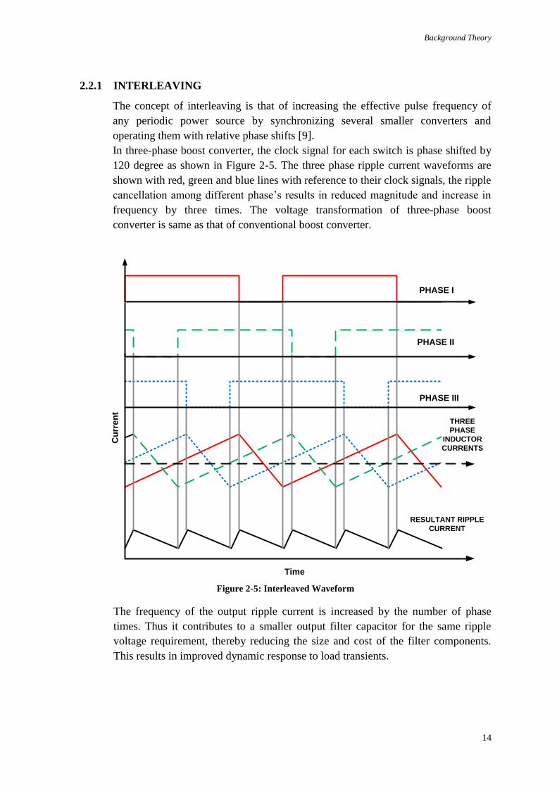
2.2.1 INTERLEAVING
The concept of interleaving is that of increasing the effective pulse frequency of
any periodic power source by synchronizing several smaller converters and
operating them with relative phase shifts [9].
In three-phase boost converter, the clock signal for each switch is phase shifted by
120 degree as shown in Figure 2-5. The three phase ripple current waveforms are
shown with red, green and blue lines with reference to their clock signals, the ripple
cancellation among different phase’s results in reduced magnitude and increase in
frequency by three times. The voltage transformation of three-phase boost
converter is same as that of conventional boost converter.
PHASE I
PHASE II
PHASE III
RESULTANT RIPPLE
CURRENT
THREE
PHASE
INDUCTOR
CURRENTS
Time
Cu
rre
nt
Figure 2-5: Interleaved Waveform
The frequency of the output ripple current is increased by the number of phase
times. Thus it contributes to a smaller output filter capacitor for the same ripple
voltage requirement, thereby reducing the size and cost of the filter components.
This results in improved dynamic response to load transients.

Background Theory
15
2.2.2 STEADY STATE ANALYSIS OF THE THREE-PHASE BOOSTER
Inductor volt-sec balance states that the average voltage across the inductor i.e. the
voltage over on period of the switching cycle is zero. Similarly, by capacitor-
charge balance the average current through a capacitor is zero [10], [27].
Considering only one phase at a time,
During ON state,
During OFF state,
As we know, from inductor volt-sec balance,
From and
Thus the output voltage for Multi – Phase Booster is given by,
INDUCTOR CURRENT IN EACH PHASE
By using the current charge balance i.e. the average capacitor current is zero over
one switching period,
During ON state,
During OFF state,
Now,

Background Theory
16
Using and , the inductor current is given by,
INDUCTOR RIPPLE CURRENT Phase Inductor current slope during ON state,
CAPACITOR RIPPLE VOLTAGE
Capacitor voltage change during sub-interval
due to multi-phasing is
given by,
Capacitor voltage change during sub-interval is given by
2.3 DESIGN – MULTI-PHASE MULTI-STAGE BOOSTER
The Multi-Phase Multi-Stage booster is designed for specifications given in Table 1,
Table 1: Multi-Phase Multi-Stage Booster design specifications
Input Voltage 12 Volts
Output Voltage 402 Volts
Rated Power 700 Watts

Background Theory
17
The converter is designed to operate in continuous conduction mode for better
operational characteristics. Three-Stage boost converter topology is chosen of which
the first stage is Multi-Phased to three phases.
2.3.1 STATIC GAIN
From the static gain of Three-Phase Three-stage booster is given as,
Where D is switch duty cycle.
Therefore, the nominal duty cycle comes out to be 0.69
Using and each stage output voltages are calculated,
First stage output voltage,
Second stage output voltage,
Third stage output voltage,
2.3.2 EQUIVALENT LOAD AT EACH STAGE
Background Theory
18
2.3.3 INDUCTANCE AND CAPACITANCE
Inductance and capacitance is calculated based on the assumed inductor ripple
current and capacitor ripple voltage respectively. The calculated inductance and
capacitance values are rounded off near to the standard available values.
2.3.3.1 STAGE I
The stage I is Multi-Phase boost Converter. The design values for Multi-Phase
boost converter are calculated and the results are verified by Matlab Simulation.
Using inductor current through each phase is given by,
– Number of phases.
Considering 70% peak to peak ripple, the single phase inductor ripple current is,
Using single phase inductance is calculated as,
For 2% ripple voltage, using the capacitance value is given by,
The resultant peak-to-peak ripple current through the capacitor, is given by
.
2.3.3.2 STAGE II
The stage II is Single-Phase boost Converter.
The stage II single phase inductor current is given by,

Background Theory
19
Considering 70% duty cycle, the inductor value is given by, using
For 2% ripple voltage, the capacitance value is given by, using (2.12)
2.3.3.3 STAGE III
The stage III is Single-Phase boost Converter. IGBT is used as a semiconductor
switching device in stage III in order to incorporate high voltage switching [17].
Unlike Mosfet, IGBT’s do not permit high switching frequencies, thus the
switching frequency is reduced to 20 kHz.
The third stage inductor current is given by,
Considering 70% duty cycle, the inductance is given by
For 2% ripple voltage, the capacitance value is given by,

Background Theory
20
2.4 SIMULATION VERIFICATION OF MULTI-PHASE MULTI-STAGE
DESIGN
The design procedure evaluated in the section 2.3 is verified by the simulating the
Multi-Phase Multi-Stage booster circuit in Mat-Lab program. The circuit was
modelled in Simulink as shown in Figure, using Sim power system blocks. The
model includes DC resistance of inductor, ESR of capacitor and semiconductor
switch ON resistance to have the parasitic effect on the system performance.
Figure 2-6: Simulink Model - Three Phase Three Stage Booster
Stage I and Stage II MOSFET’S are switched at 100 kHz frequency. The stage III
of the model uses IGBT which is switched at 20 kHz instead of MOSFET to
incorporate high voltage switching. Considering Hardware design, the availability
of high voltage rated silicon based MOSFET is rare. Nowadays, Silicon Carbide
based MOSFET are available which can switch high voltage but they are
expensive. Thus IGBT is a better solution to be used for high voltage switching, but
it is switched comparatively at lower frequency because of its characteristics tailing
phenomenon3 [17]. Due to capacitive ESR, the output voltage ripple may be higher
than the assumed one, thus it is better to chose higher capacitance than the
calculated value [12].
The simulation results for stage I – three phase inductor currents and
resultant current is shown in Figure 2-7. All the three – phase inductor currents
settles within 5 ms with initial transients.
3 The tailing phenomenon is the tailing collector current due to the stored charge in drift region. The tail
current increase the turn – off loss and requires an increase in the dead time insertion, which eventually
reduces the effective switching frequency.

Background Theory
21
Figure 2-7: Stage I Three Phase Inductor currents
The Interleaved stage – I three phase current and their resultant reduced ripple
current is given in Figure 2-8.
Figure 2-8: Interleaved Three Phase Inductor currents
From the Figure 2-8, it is evident that the magnitude of resultant ripple current
flowing into the output capacitor got much reduced than the phase ripple current
0 0.005 0.01 0.015 0.02 0.025 0.03 0.035 0.04
0
100
200(a) Inductor Current Phase I
0 0.005 0.01 0.015 0.02 0.025 0.03 0.035 0.04
0
100
200(b) Inductor Current Phase II
0 0.005 0.01 0.015 0.02 0.025 0.03 0.035 0.04
0
100
200(c) Inductor Current - Phase III
0 0.005 0.01 0.015 0.02 0.025 0.03 0.035 0.04
0
200
400
Time
(d) Resultant ripple Current
IL11
IL12
IL13
IL
0 0.005 0.01 0.015 0.02 0.025 0.03 0.035 0.04
0
100
200
Cu
rren
t (A
)
(a) Inductor Current Phase I
0 0.005 0.01 0.015 0.02 0.025 0.03 0.035 0.04
0
100
200
Cu
rren
t (A
)
(b) Inductor Current Phase II
0 0.005 0.01 0.015 0.02 0.025 0.03 0.035 0.04
0
100
200(c) Inductor Current - Phase III
Cu
rren
t (A
)
0 0.005 0.01 0.015 0.02 0.025 0.03 0.035 0.04
0
200
400
Time
Cu
rren
t (A
)
(d) Resultant ripple Current
IL1
1.46 1.465 1.47 1.475 1.48 1.485 1.49 1.495 1.5
x 10-3
10
15
20
25
30
35
40
45
50
55
Time
Cu
rre
nt
(A)
Interleaved Three-Phase Inductor Current
IL11
IL12
IL13
IL1
1.46 1.465 1.47 1.475 1.48 1.485 1.49 1.495 1.5
x 10-3
10
15
20
25
30
35
40
45
50
55
Time
Cu
rre
nt
(A)
Interleaved Three-Phase Inductor Current
Interleaved Phase Currents
Reduced resultant ripple current

Background Theory
22
due to three – phase interleaved switching and also the ripple frequency increased
by 3 times i.e. the total number of phase times.
The stage II and stage III inductor current waveform is shown in figure 2-9. The
stage II and stage III inductor settles within 8 ms with initial transients.
Figure 2-9: Stage II and Stage III Inductor currents
The three stage output voltages are shown in Figure 2-10. All the three stage
voltages get settles at around 10 ms with initial transients.
Figure 2-10: Three Stage Output Voltages
0 0.005 0.01 0.015 0.02 0.025 0.03 0.035 0.04
0
50
100
(a) Stage II Inductor Current
0 0.005 0.01 0.015 0.02 0.025 0.03 0.035 0.04
0
10
20
30
(b) Stage III Inductor current
IL2
IL3
0 0.005 0.01 0.015 0.02 0.025 0.03 0.035 0.04
0
50
100
Cu
rren
t (A
)
0 0.005 0.01 0.015 0.02 0.025 0.03 0.035 0.04
0
10
20
30
Time
Cu
rren
t (A
)
0 0.005 0.01 0.015 0.02 0.025 0.03 0.035 0.0410
20
30
40
50
a) Stage I Output Voltage
0 0.005 0.01 0.015 0.02 0.025 0.03 0.035 0.04
50
100
150
b) Stage II Output Voltage
Vo
lta
ge
0 0.005 0.01 0.015 0.02 0.025 0.03 0.035 0.04
200
400
600
Time
c) Stage III Outpt Voltage
V1
V2
V3
0 0.005 0.01 0.015 0.02 0.025 0.03 0.035 0.0410
20
30
40
50
Vo
lta
ge
0 0.005 0.01 0.015 0.02 0.025 0.03 0.035 0.04
50
100
150
0 0.005 0.01 0.015 0.02 0.025 0.03 0.035 0.04
200
400
600
Vo
lta
ge
Background Theory
23
The transient and steady state response can be improved effectively by using control
system [32], [18], [21] which will be discussed in the next section. By adopting a soft-
start mechanism to the system, the high inrush transient current can be avoided and
stresses on the semiconductor switches can be reduced [24].
As the stage III is switched at 20 kHz, that frequency component is reflected back on
stage II output. The output waveform of stage II is superimposed with 20 kHz
frequency component. If the output filter capacitance is increased, the settling time of
stage III may get increased.
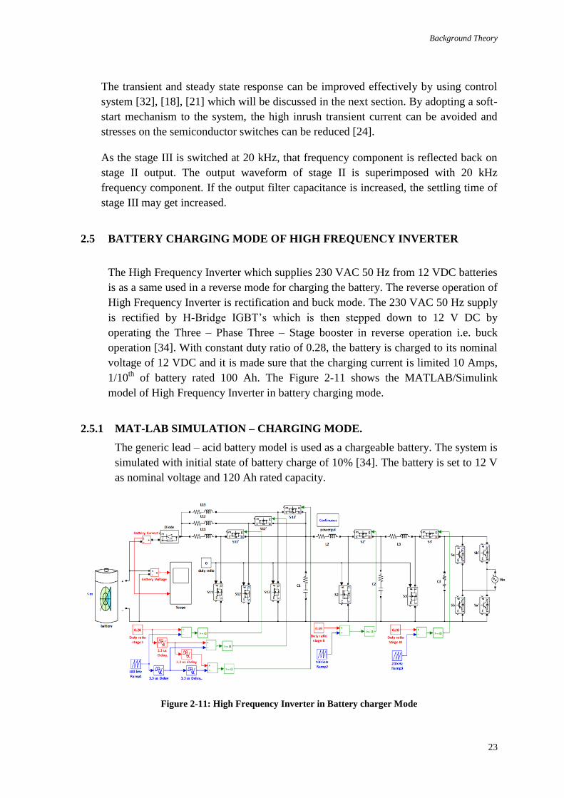
2.5 BATTERY CHARGING MODE OF HIGH FREQUENCY INVERTER
The High Frequency Inverter which supplies 230 VAC 50 Hz from 12 VDC batteries
is as a same used in a reverse mode for charging the battery. The reverse operation of
High Frequency Inverter is rectification and buck mode. The 230 VAC 50 Hz supply
is rectified by H-Bridge IGBT’s which is then stepped down to 12 V DC by
operating the Three – Phase Three – Stage booster in reverse operation i.e. buck
operation [34]. With constant duty ratio of 0.28, the battery is charged to its nominal
voltage of 12 VDC and it is made sure that the charging current is limited 10 Amps,
1/10th
of battery rated 100 Ah. The Figure 2-11 shows the MATLAB/Simulink
model of High Frequency Inverter in battery charging mode.
2.5.1 MAT-LAB SIMULATION – CHARGING MODE.
The generic lead – acid battery model is used as a chargeable battery. The system is
simulated with initial state of battery charge of 10% [34]. The battery is set to 12 V
as nominal voltage and 120 Ah rated capacity.
Figure 2-11: High Frequency Inverter in Battery charger Mode

Background Theory
24
2.5.2 BATTERY CHARGING VOLTAGE AND CURRENT
Diode is connected in series with battery in order to avoid battery discharge i.e. the
backward flow of current. The system was simulated for 160 ms and the charging
voltage waveform of battery is shown in Figure 2-12. It is evident from the
waveform that the battery is being charged, the ramp up of charging voltage as
shown in Figure 2-12.
Figure 2-12: Battery charging voltage
The battery charging current waveform is shown in Figure 2-13. It can be observed
the battery is charged with average current of 10 A, and due to multi-phasing and
interleaved switching, the resultant ripple in charging current is reduced to 20%.
Figure 2-13: Battery charging current
0 0.05 0.1 0.159.108
9.11
9.112
9.114
9.116
9.118
9.12
9.122
9.124
9.126
Time
Vo
lta
ge
Battery Charging Voltage
0 0.05 0.1 0.159.108
9.11
9.112
9.114
9.116
9.118
9.12
9.122
9.124
9.126
Time
Vo
lta
ge
Battery Charging Voltage
0 0.05 0.1 0.150
2
4
6
8
10
12
Time
Cu
rre
nt
Battery Charging Current
0 0.05 0.1 0.150
2
4
6
8
10
12
Time
Cu
rre
nt

Background Theory
25
With Multi-Phase charging mode, the charging ripple current is much reduced
compared to other converter topology charging current, thus it leads to better life –
period of battery.
In charging mode only the high side switch of Three - Phase Three – Stage booster
need to be controlled, all the low side switch will be inactive. The inherited diode
of MOSFET’s will do the free-wheeling action for buck operation.

Methodology
27
3 METHODOLOGY
The Power Converter Systems invariably require feedback. In a typical dc-dc
converter application, the output voltage must be kept constant, regardless of
changes in the input-voltage or in the effective load resistance [13], [25]. This
is accomplished by building a circuit that varies the converter control input i.e., the
duty cycle in such a way that the output voltage is regulated to be equal to
a desired reference value . So the feedback system is commonly employed. This
chapter includes the small signal ac-modeling and closed loop control of Single Phase
and Multi-Phase Boost Converter with Type III compensator employed [32], [23]. It
also discusses the effect of RHP zero in typical boost converter [19], [21].
3.1 INTRODUCTION – MODELING AND CONTROL
A typical Boost converter incorporating a Feedback loop is illustrated in Figure 3-
1. It is desired to design this feedback system in such a way that the output voltage
is accurately regulated, and is insensitive to disturbances in or the load
current. In addition the feedback system should be stable, and properties such as
transient overshoot, settling time and steady – state regulation should meet
specifications [15], [30]. Thus, it is required to build a circuit that adjust the duty
cycle as necessary to obtain the specified output voltage regardless of disturbances
and component tolerance. The negative feedback control technique is adopted to
feed the sensed output voltage to the controller which in turn adjusts the duty cycle
to have a constant output voltage [19], [23].
Vg
rl L
ron1C
Driver
ron2
rc
Load
Vref
+
_
S1
S2
Vc
d
GcPWM
Figure 3-1: Voltage Mode Controlled Boost Converter

Methodology
28
A linear control technique can be applied to a linear system, but all the switch mode
system are non-linear system4 [13], [14]. So, the system needs to be modelled as a
linear system, in order to apply a linear control technique. The objective of the small
signal ac converter modeling is to predict how low-frequency variations in duty cycle
induce low frequency variations in the converter voltages and currents. The ac
converter model can be achieved by removing switching harmonics by averaging all
waveforms over one switching period. An averaged model implies the disappearance
of any switching event to the benefit of a smoothly varying continuous signal [22].
The averaged voltages and currents are, in general, nonlinear functions of the
converter duty cycle, voltages, and currents and constitute a system of nonlinear
differential equations.
3.2 SMALL SIGNAL AC MODELING OF BOOST CONVERTER
State Space averaging method is approached to have a small signal ac-model of
Boost converter. The derivatives of state space variables are expressed as linear
combinations of the system independent inputs and state-variables themselves. The
physical state variables are the inductor currents and the capacitor voltages [13],
[26]. The boost converter is modelled including inductor copper loss i.e. DC
resistance of Inductor, Equivalent series resistance (ESR) of filter capacitor and ON
resistance of semiconductor switches.
3.2.1 SUB-INTERVAL I
During sub-Interval I, the boost converter is reduced to a linear circuit as shown in
Figure 3-2. The switch is closed, while the switch is open. During this sub-
Interval of switching period, the inductor will store the energy and the capacitor
supplies to the load. The derivatives of the state variables are expressed for the
reduced linear circuit as shown in Figure 3-2.
L
ron1
C
rc
RVg
rl
Figure 3-2: Sub-Interval I
4 The switch mode power supplies are non-linear system as the circuit during one sub-Interval I is not the
same for sub-Interval II.

Methodology
29
The voltage across the inductor is given as,
The capacitor current is given by,
The output voltage is given as,
3.2.2 SUB-INTERVAL II
During sub-Interval II, the boost converter is reduced to a linear circuit as shown in
Figure 3-3. The switch is closed, while the switch is open. The stored energy
in the inductor charges the capacitor and is supplied to the load.
L
C
Vg
rc
rl ron2
R
Figure 3-3: Sub-Interval II
The linear circuit during sub-interval II as shown in Figure 3-3 is analyzed,
The voltage across inductor is given as,
Now, for capacitor current,

Methodology
30
Output Voltage is given as,
The approximations in above equation are,
as ,
Here after, as
The equation in state-space form for Sub-Interval I is derived from and ,
From , the Output equation in state space form for Sub-Interval I,
The state matrix for sub-Interval I,
Input Vector for sub-Interval I
Output matrix for sub-Interval I
The equation in state space for Sub – Interval II, is derived from and

Methodology
31
From , the output equation in state space form for sub-Interval II
State matrix for sub-Interval II,
The input vector for sub-Interval II
The output matrix for sub-Interval II
From steady state analysis of conventional boost converter, we know,
Including the copper loss and semiconductor losses,
and the inductor current is given by,
The capacitor voltage is approximated as,
Now, the linearized state equation is obtained by dropping out the DC and second
order non-linear term, and is given by,
Methodology
32
Where,
and,
Similarly, the linearized output equation is given by,
Converting into Laplace form and simplifying,
Where, and
With the help of , (3.13) and , the transfer function for boost
converter – Control to Output is given as,
Where, the DC gain,
The resonant frequency
The Quality factor,
The Right Half plane zero frequency,
The Equivalent Series Resistance zero frequency,

Methodology
33
3.3 RIGHT HALF PLANE ZERO IN BOOST CONVERTER
From the above control to output transfer function , it is evident that the boost
converter offers a set of complications – a right half plane zero (RHP) in analysis and
characteristics. It can be a challenging converter to stabilize when operating with
voltage mode control. RHP5 zero is caused by a fact that when the boost converter
switch is turned on for a longer period of time. That means the output initially drops,
even though the control command is trying to make it increase [16], [32].
This is exactly the characteristics of a classic RHP zero. An increase in the
command signal to the control system causes an initial decrease in the output
response. After the time constant associated with the RHP zero has elapsed, the
output starts moving in the same direction as the control [14]. As a result, if you have
a system with a RHP zero in the control to output transfer function, you cannot
expect the control loop to respond immediately to changes in the output. The
bandwidth of the loop must be limited to considerably less than the frequency of the
RHP zero if the system is to be stabilized properly [14].
3.4 COMPENSATION FOR VOLTAGE MODE BOOST CONVERTER
Closing the control loop allows the regulator to adjust to load perturbations or
changes in the input voltage which may adversely affect the output. Proper
compensation of the system will allow for a predictable bandwidth with
unconditional stability [32], [19].
3.4.1 TYPE III COMPENSATOR
In most cases, a Type III compensation network will properly compensate the
system. The ideal Bode plot for the compensated system would be a gain that rolls
off at a slope of -20dB/decade, crossing 0 db at the desired bandwidth6 and a phase
margin greater than for all frequencies below the 0 dB crossing [22], [20].
R3C3
R2C2
C1
R1
_
+Vo
Vi
Figure 3-4: TYPE III Compensator
5 In Frequency response, Right Half Plane zero contributes a gain of +20dB/decade, while the phase of .
6 Wide bandwidth results in better transient response.

Methodology
34
Figure 3-4 shows a generic Type III compensator, its transfer function is given as in
equation 3.20. The Type III network shapes the profile of the gain with respect to
frequency. The Type III Compensation, however, utilizes two zeroes to give a phase
boost of . This boost is necessary to counteract the effects of an under damped
resonance of the output filter at the double pole [18].
3.4.2 BOOST CONVERTER VOLTAGE MODE CHARACTERISTICS
It can be noted that the boost converter in its voltage mode control have four
main characteristics a double pole due to the LC filter which moves with operating
conditions, an ESR zero due to equivalent series resistance of output capacitor, a
RHP zero which moves with the operating conditions and finally a variable gain
dependent upon the input voltage of the boost converter. These characteristics are
taken into considerations in the placement of poles and zeros of type III compensator
[14]. So, here the first pole of the compensator is placed at the origin to form an
integrator to have high DC gain7. Compensator zeros are placed around the power
stage resonant frequency8. The second pole of the compensator is placed coincident
with the ESR zero frequency of the power stage. The third pole of the compensator is
placed coincident with the RHP zero frequency of the power stage. If the RHP zero
or ESR zero is higher than the switching frequency, the corresponding compensation
poles are placed at half the switching frequency [14].
3.5 CLOSED LOOP CONTROL – STAGE II AND STAGE III
The stage II and stage III of the Three – Phase Three –Stage booster is a single phase
conventional boost converter. Thus the small – signal ac modelled booster in section
3.2 can be used to aid the design of an individual compensated control for each stage
II and stage III. Stage I is not applicable as it multi-phased, thus it is separately
modelled and compensator is designed in section 3.6. The compensated system
results in enough phase and gain margin with desired bandwidth. The power
specification and component values of designed Multi – Phase Multi – Stage system
in Table 2 is used for designing a controller.
7 High DC gain leads to a small steady – state error and tight voltage regulation
8 For compensating phase delay due to integrator and double pole

Methodology
35
The power stage specification for stage II and stage III as given in table 2.
Table 2: Power Stage specifications for stage II and III
Stages Inductance DC Resistance
Inductor Capacitance
ESR of
Capacitor
Switch ON
Resistance
Stage II 21.1 uH 5 mΩ 18 uF 10 mΩ 20 mΩ
20 mΩ
Stage III 1.1 mH 5 mΩ 630 uH 10 mΩ 20 mΩ
20 mΩ
Using , the bode plot for control – to – output transfer function of stage II is
generated with the help of Malt-Lab program as shown in Figure 3-5. From the
Figure 3-5, the frequency of resonant peaking, Right Half Plane zero and ESR zero
are noted in order to design compensator. The right half plane zero causes the phase
angle to dip by 90 degrees is clearly evident from the Figure 3-5.
Figure 3-5: Stage II control-to-output transfer function
The compensated system designed need to be with enough phase margin and
bandwidth for better closed loop performance. The double zero of type III
Compensator is placed at the resonant frequency. First pole is placed at origin
(Integral action) to have a high DC gain; second pole at frequency of RHP zero and
the third pole placed at half the switching frequency 50 kHz. The Figure 3.6 shows
the compensated frequency response of Multi-Phase Boost Converter.
-20
0
20
40
60
80
Ma
gn
itu
de
(d
B)
102
103
104
105
106
107
108
90
135
180
225
270
315
360
Ph
as
e (
de
g)
Stage II - Uncompensated
Gm = 14.9 dB (at Infinite Hz), Pm = -73.7 deg (at 163 kHz)
Frequency (Hz)
102
103
104
105
106
107
108
90
135
180
225
270
315
360
Ph
as
e (
de
g)
-20
0
20
40
60
80
Ma
gn
itu
de
(d
B)
Double pole, 2.53 kHz
Maximum phase lag due to RHP zero
ESR zero, 884.2 kHz
Right Half plane zero, 16.14 kHz
Methodology
36
Figure 3-6: Stage II Compensated Bode plot
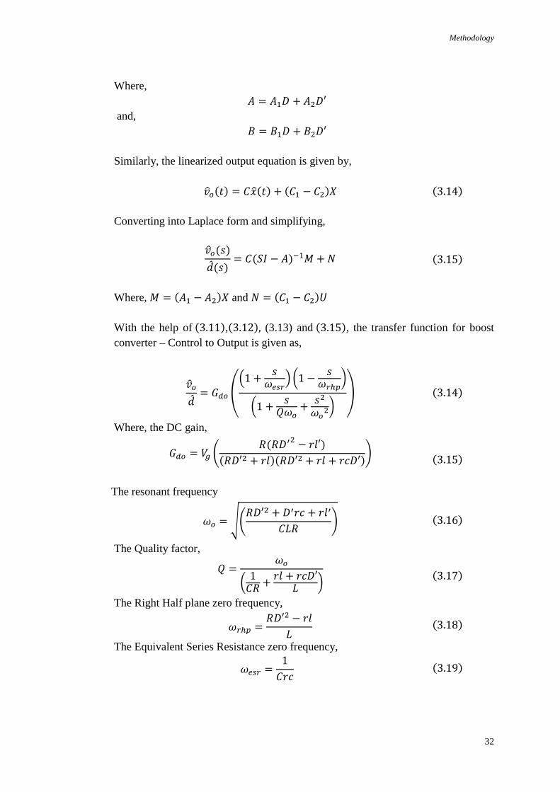
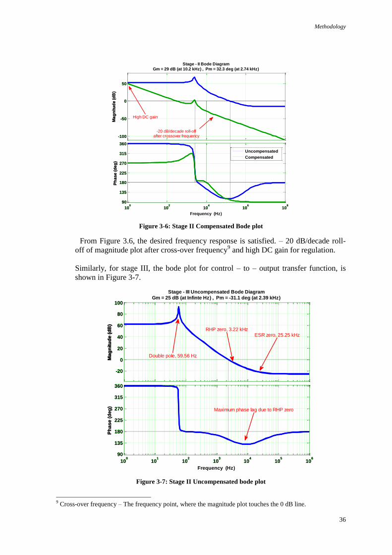
From Figure 3.6, the desired frequency response is satisfied. – 20 dB/decade roll-
off of magnitude plot after cross-over frequency9 and high DC gain for regulation.
Similarly, for stage III, the bode plot for control – to – output transfer function, is
shown in Figure 3-7.
Figure 3-7: Stage II Uncompensated bode plot
9 Cross-over frequency – The frequency point, where the magnitude plot touches the 0 dB line.
-100
-50
0
50
Ma
gn
itu
de
(d
B)
100
102
104
106
108
90
135
180
225
270
315
360
Ph
as
e (
de
g)
Stage - II Bode Diagram
Gm = 29 dB (at 10.2 kHz) , Pm = 32.3 deg (at 2.74 kHz)
Frequency (Hz)
Uncompensated
Compensated
100
102
104
106
108
90
135
180
225
270
315
360
Ph
as
e (
de
g)
-100
-50
0
50
Ma
gn
itu
de
(d
B)
High DC gain
-20 dB/decade roll-offafter crossover frequency
100
101
102
103
104
105
106
90
135
180
225
270
315
360
Ph
as
e (
de
g)
Stage - III Uncompensated Bode Diagram
Gm = 25 dB (at Infinte Hz) , Pm = -31.1 deg (at 2.39 kHz)
Frequency (Hz)
-20
0
20
40
60
80
100
Ma
gn
itu
de
(d
B)
100
101
102
103
104
105
106
90
135
180
225
270
315
360
Ph
as
e (
de
g)
-20
0
20
40
60
80
100
Ma
gn
itu
de
(d
B)
ESR zero, 25.25 kHzRHP zero, 3.22 kHz
Maximum phase lag due to RHP zero
Double pole, 59.56 Hz

Methodology
37
For compensated bode plot for stage III, is shown in figure. The bandwidth
for the stage III is not as high as compared to stage II due to high value of
Inductance and capacitance.
Figure 3-8: Stage III compensated system
-50
0
50
100
Ma
gn
itu
de
(d
B)
100
101
102
103
104
105
106
90
180
270
360
Ph
as
e (
de
g)
Stage - III Compensated Bode plot
Gm = 25.5 dB (at 3.1 kHz) , Pm = 50.2 deg (at 198 Hz)
Frequency (Hz)
Uncompnesated
Compensated
100
101
102
103
104
105
106
90
180
270
360
Ph
as
e (
de
g)
-50
0
50
100
Ma
gn
itu
de
(d
B)
High DC Gain
-20 dB/decade roll-offafter crossover frequency

Methodology
38
3.6 MULTI-PHASE BOOST CONVERTER MODELING
Multi-Phase boost converter is attained by adding parallel legs to the conventional
boost converter. Unlike conventional boost converter which has two states during
each switching period, due to interleaved switching sequence of Multi-Phase Boost
Converter, it undergoes various different states depending on the number of phase.
The duration of each state is derived with relative to its duty ratio and the switching
period.
rl1L1
S1
ron1
C
rl2L2
rl3L3
ron2 ron3
S2 S3
S1'
S2'
S3'
rcVg
ron1'
ron2'
ron3'
R
Figure 3-9: Three-Phase Boost Converter
3.6.1 MODELLING OF THREE-PHASE BOOST CONVERTER
The Three-Phase boost converter as shown in Figure:3.9 is operated in continuous
conduction mode for better operational characteristics results. In Three-Phase Boost
converter, the different phase switches are operated with relative phase shifts which
are 120 degree apart. The switch operates in complementary to switches
respectively.
3.6.2 INTERLEAVED SWITCHING SEQUENCE
The gate pulse for interleaved three-phase boost converter is shown Figure: 6. Due
to interleaved switching of the system exhibits 6 states in one switching period.
Different switching states are tabulated in Table.3. The state I, III and V lasts
for , while state II IV VI lasts for (1-D) of the switching period .

Methodology
39
PHASE I
PHASE II
PHASE III
Ts
(D-2/3)Ts(1-D)Ts
I II III IV V VI
Figure 3-10: Interleaved Switching Gate Pulse
Table 3: Switch position for different states
States S11 S12 S13 S21 S22 S23
I 1 1 1 0 0 0
II 1 0 1 0 1 0
III 1 1 1 0 0 0
IV 1 1 0 0 0 1
V 1 1 1 0 0 0
VI 0 1 1 1 0 0
1 – Switch ON
0 – Switch OFF
3.6.3 STATE I III V
It can be noted from Table no. 3 that States I, III and V are similar to each other.
These states can be described with help of Figure: 3.11. Where all the three
switches are closed and switches are open, the capacitor
supplies the stored energy to the load.

Methodology
40
rl1L1
ron1
C
rl2L2
rl3L3
ron2 ron3
Rrc
Vg
Figure 3-11: State I II III
It is approximated that,
as
Here after, ; ;
The equation in state space form for States I II III can be given as,
The output state equation,

Methodology
41
3.6.4 STATE II
In state II, the second phase switch is opened and its complementary is
closed as shown in Figure: 3.12. Thus, the stored energy in is supplied to the
load, while L1 and L2 continue to store energy.
rl1L1
ron1C
rl2L2
rl3L3
ron3R
ron2'
rc
Vg
Figure 3-12: State II
The equation in state space form for state II is given as,
....
The output matrix is given as,

Methodology
42
3.6.5 STATE IV
In state IV, the third phase switch is opened and its complementary is
closed as shown in Figure:3.13. Thus, the stored energy in is supplied to the
load.
rl1L1
ron1C
rl2L2
rl3L3
ron2R
ron3'
rc
Vg
Figure 3-13: State IV
The equation in state space form for state IV is given as,
....
The output equation is given as,

Methodology
43
3.6.6 STATE VI
In state VI, the first phase switch is opened and its complementary is
closed as shown in Figure:3.14. Thus, the stored energy in is supplied to the
load.
rl1L1
C
rl2L2
rl3L3
ron1 R
ron1'
rc
ron2Vg
Figure 3-14: State VI
The equation in state space form for state IV is given as,
......... (3.36)
The output equation is given as,

Methodology
44
3.6.7 AVERAGING – STATE MATRIX OF THREE PHASE BOOSTER
The Averaged state matrix is given by,
Equilibrium DC State Vector,
Equilibrium DC Input Vector,
Now, the perturbed and linearized small-signal state equation is given by,
Where,
Similarly, the linearized output equation is given by,
Where,
In case of Three-Phase Boost converter,
and
Similarly,
Simplifying the linearized equation and converting it into Laplace form,

Methodology
45
So, by Laplace transform,
Using to
Where,
DC gain is given by,
The resonant frequency,
The Quality factor,
The Right Half Plane zero (RHP),
The ESR zero,

Methodology
46
3.7 CLOSED LOOP CONTROL – MULTI-PHASE BOOST CONVERTER
Using the frequency response (Bode Plot) is obtained for Multi-Phase Boost
Converter as shown in Figure: 3-15. From the Figure: 3-15 the frequency at which
resonating peak, Right Half Plane zero and ESR zero are noted in order to design
compensation. The right half plane zero causes the phase angle to dip by 90 degrees
is clearly evident from the Figure: 3-15.
Figure 3-15: Stage I - Uncompensated bode plot
The Figure: 3-16 shows the compensated frequency response of Multi-Phase Boost
Converter. The double zero of type III Compensator is placed at the resonant
frequency. First pole is placed at origin (Integral action) to have a high DC gain;
second pole at frequency of RHP zero and the third pole placed at half the
switching frequency 50 kHz.
0
10
20
30
40
50
60
Ma
gn
itu
de
(d
B)
101
102
103
104
105
106
107
90
135
180
225
270
315
360
Ph
as
e (
de
g)
Stage - I Uncompensated Bode Plot
Gm = 4.68 dB (at Infinite Hz) , Pm = -49.2 deg (at 205 kHz)
Frequency (Hz)
0
10
20
30
40
50
60
Ma
gn
itu
de
(d
B)
101
102
103
104
105
106
107
90
135
180
225
270
315
360
Ph
as
e (
de
g)
RHP zero, 16.2 kHz
ESR zero, 284 kHz
Double pole, 4.63 kHz
Maximum phase delay due to RHP zero

Methodology
47
Figure 3-16: Stage I Compensated system
Three individual compensators have been used for three different stages of Multi-
Phase Multi-Stage boost converter in order to control each stage independently.
Otherwise, three-stage booster collectively exhibits 6th
order system, compensating
such higher order system is very difficult. Once all the compensated stages are
combined, there may be need to adjust the gain of the compensator for better
frequency response.
-80
-60
-40
-20
0
20
40
60
80
Ma
gn
itu
de
(d
B)
100
101
102
103
104
105
106
107
90
135
180
225
270
315
360
Ph
as
e (
de
g)
Stage - III Compensated Bode Diagram
Gm = 10.4 dB (at 6.97 kHz) , Pm = 49.8 deg (at 4.78 kHz)
Frequency (Hz)
Uncompensated
Compensated
-80
-60
-40
-20
0
20
40
60
80
Ma
gn
itu
de
(d
B)
100
101
102
103
104
105
106
107
90
135
180
225
270
315
360
Ph
as
e (
de
g)
High DC Gain
- 20 dB/decade roll-offafter crossover frequency

Result Analysis
48
4 RESULT ANALYSIS
The system is analysed, modelled and simulated in Mat-Lab/Simulink program to
analyse the various significant results of Multi-Phase Multi-Stage booster. Based on
the Mat-Lab results, hardware design will considered and the required components
should be procured. This chapter deals with the significant results in different domain
of analysis. The transient and frequency responses were analysed in detail to
understand the behaviour of the system under different operating conditions.
4.1 TRANSIENT RESPONSE
From time domain response of system in section 3.2, it was clear the settling time of
the system is better, but the transient peaks of inductor currents were too high. This
high transient peak current can be a threat to semiconductor switches, as the path for
this current is through switches to ground. These transients need to be avoided for safe
operation. Due to independent control system for each stage, the feedback error
initially jumps to its maximum. The large feedback error then drives the loop filter to
its limit, which drives the power switching transistors in the driver section of the
power supply at their maximum rating. This condition continues until the output
voltage of the power supply approaches its nominal value. Thus, using soft-start
technique, the system transient can be avoided. Soft-start circuits alleviate this
problem by ramping up the output of the power supply at a slower rate. The reduced
rate limits the initial error and the overall drive of the system is reduced.
The transient response due to load variation is kept under control by sensing the
output voltage and feeding it back to the controller which in turn derives the duty ratio.
4.2 SYNCHRONOUS SWITCHING
Many DC-DC converters use a MOSFET in place of the diode. The advantage of this
configuration is that the second MOSFET will have a much lower voltage drop across
it compared to a diode, resulting in higher circuit efficiency. This is especially
important in low-voltage, high-current applications. The Figure 4-1 shows the power
loss due diode compared with MOSFET. A Shottky diode would have a voltage of 0.3
to 0.4 V across it while conducting, whereas a MOSFET will have an extremely low
voltage drop due to an Rds-ON as low as single-digit milliohms. This circuit has a
control scheme known as synchronous switching, or synchronous rectification. The
two MOSFETs must not be on at the same time to prevent a short circuit across the
source, so a “dead time” is built into the switching control – one MOSFET is turned
off before the other is turned on. The inherent diode parallel to the MOSFET will
provide a conducting path for inductor current during the dead time when both
MOSFETs are off. This diode may be the MOSFET body diode, or it may be an extra

Result Analysis
49
diode, most likely a Shottky diode, for improved switching. The synchronous buck
converter should be operated in the continuous-current mode because the MOSFET
would allow the inductor current to go negative.
Figure 4-1: Power Loss compared with synchronous switching
The control loop designed is for system operating in continuous conduction mode
(CCM), and moreover with synchronous switching the diode is replaced with
MOSFET switch, which conduct on both direction, bidirectional device. Thus the
system should be operated in only CCM mode and DCM operation should be
avoided. As the inductor current reaches to its boundary condition, the
complementary pulse that feeds the synchronous Mosfet should be stopped, in order
to avoid current source back to battery, but still the system can function because of
the MOSFET’s inherited diode.
4.3 FREQUENCY RESPONSE
The bode plot generated for the small – signal ac model of boost converter revealed
the non-minimum phase system characteristics. The RHP zero in the non-minimum
phase system created the complication in compensating the boost converter. With
1 2 3 4 5 6 7 8 9 100
1
2
3
4
5
6
7
8
Load Current (A)
Po
we
r L
os
s
Power Loss compared with synchronous switching
1 2 3 4 5 6 7 8 9 100
1
2
3
4
5
6
7
8
Load Current (A)
Po
we
r L
os
s
Power Loss compared with synchronous switching
Power Loss due to Diode
Power Loss due to MOSFET (Synchronous Switching)

Result Analysis
50
Type III compensator employed, the effect of maximum phase lag due to RHP is
minimized. With appropriate pole and zero placement of the type III compensator,
the compensated system with enough phase margin and bandwidth were attained.
Generally phase margin is enough for a compensated system, but by adopting a
digital control system, extra phase lag is added due to sampling time, propagation
delay of the digital output and finite MIPS of control IC for execution of control
algorithm. Thus it desired to have better phase margin of above Bandwidth is
generally kept to be high around 1/10th
of the switching frequency to have a small
settling time.
4.4 HARDWARE DESIGN BASED ON SIMULATION RESULTS
The time domain results of the system are used to aid in Hardware design and
component selection. The voltage and current rating of the selected MOSFET should
be at least twice the required rating as per the thumb rule adopted in many industries.
While selecting the inductor its saturation current limit and the frequency should be
thoroughly considered. As the inductor current rises above the saturation current
limit, the inductance reduces and causes the system to operate in discontinuous mode
and controlling such system becomes too difficult. The system simulations include
the DC resistance of the inductor, ESR of capacitor, Rds ON of semiconductor
switch, to have the parasitic effect. The output capacitance of the stage III needs to
be of higher value then the calculated, as its output DC voltage will be inverted to
AC voltage by SPWM Inverter. While charging the battery, output capacitance of the
rectifier need to be large so that smooth DC can be obtained. There is no requirement
of control loop for system in battery charging mode. Predefined constant duty ratio
for the desired charging current is the only requirement for the system in charging
mode. The film capacitance is recommended to handle high capacitor current.

Conclusion & Future Scope of Work
51
5 CONCLUSIONS & FUTURE SCOPE OF WORK
5.1 WORK CONCLUSION
The work presented in this thesis explored the Multi-Phase Multi-Stage booster
topology for High Frequency Inverter application, which eventually replaced the high
frequency step-up transformer. The thesis discusses the steady state analysis, small –
signal ac modelling and closed loop control of Three-Phase Three-Stage boost
converter. Issues involving in high frequency transformer for voltage boosting were
discussed. The shortcomings of alternative voltage boosting power stage topology
such as boost converter with voltage multiplier cell options were also discussed.
The Mat-Lab model of booster part for 700 watts rated power was simulated in
Mat-Lab/Simulink program in order to verify the evaluated design procedure. The
simulation included the copper loss and semiconductor losses. The concept of
interleaved switching in Multi-Phase converter which increases the effective pulse
frequency, thereby reduces the filter size is discussed and verified with Mat-Lab
simulation. The time response simulation resulted in initial transients, which is stress
on semiconductor switches. Using soft-start technique, which ramps up the output in
steady and slow rate, the initial transients can be avoided, thereby reducing the stress
on semiconductor switches.
The small–signal ac models of the Multi – Phase and Single – Phase booster
were developed to aid in the control design and analyze the characteristics Right Half
Plane zero complication. A simple voltage mode controlled booster transfer function
was derived from the developed model and frequency response were analyzed using
bode diagram. Independent control strategies were employed for individual stages for
simpler control system design. All the analysis, modeling derivation and simulation
and closed loop control design were carried out for continuous conduction mode for
better operational characteristics.
The Type III compensator was employed in compensating the system, as
maximum phase boost of can be achieved. The compensated system has a better
phase margin and closed loop performance. With integral action of Type III
compensation high DC gain is achieved for tight output voltage regulation. The
improvement in frequency response after compensation were compared using bode
plot. With proper placement of compensating poles and zeros, the RHP zero
complication is eliminated.
The battery charging mode of High Frequency Inverter in discussed where the
Inverter works as rectifier and booster in buck operation mode. The Mat-Lab
simulation of battery charger includes actual Lead-acid battery model for charging.
Thus the Multi – Phase Multi – Stage boost converter topology was studied,
analyzed and designed. Very important application of this high static gain boost
topology is found in Inverter, sourced from battery, where bulky step – up transformer
can be eventually replaced.

Conclusion & Future Scope of Work
52
5.2 FUTURE SCOPE OF WORK
The design and control procedure is proposed and 700 watts Multi-Phase Multi-Stage
booster is simulated in Mat-Lab/Simulink program. However, the experiment is not
done to verify the method. Only the voltage mode controller is adopted for
compensating and control over variation of load, however behaviour of current mode
control with Multi – phase Multi – stage system need to verified.
The digital control system needs to be developed because of its inherent flexibility,
which allows modifying the control strategy, without the need of significant hardware
reconstruction. Thus, it is required to simulate the system with discrete control blocks,
to verify the response with digital controls. The Digital signal controller can be
employed for hardware of control because on a single chip it combines the processing
power of a Digital signal processing (DSP) and the functionality of a microcontroller
with a flexible set of peripherals.
Moreover this thesis is concerned with the booster part only; the inverter
section is not analyzed and designed. Thus analysis of SPWM Inverter is required and
with appropriate control system. Employing new SPWM switching technique such as
modified unipolar switching to attain the beneficiary such as reduced switching loss
and low harmonics distortion can be a good area for research.
Last, but not the least, the Multi – Phase Multi – stage booster can be explored
to other system such as motor control, hybrid vehicle, renewable energy system and
bidirectional DC – DC conversion.

References
53
Paper presented from this work
Karuna Mudliyar, Suryanarayana K, H.V. Gururaja Rao, “Analysis of High Frequency
Multi-Phase Multi-Stage Boost Converter” International Conference on Advances &
Development in Engineering & Technology, ISBN: 978-93-81693-88-8, 8th Feb.2013,
Indore.
REFERENCES
Journal/Conference Paper
[1] Chuanyun Wang, “Investigation on Interleaved Boost Converters and
Applications”, PhD thesis, Virginia Polytechnic Institute and State University,
2009.
[2] D. Maksimovic and S. Cuk, “Switching converters with wide dc conversion
range,” Power Electronics, IEEE Transactions on, vol. 6, pp. 151–157, 1991.
[3] E.Koutroulis, J.Chatzakis, K.Kalaitzakis and N.C.Voulgaris, “A bidirectional,
sinusoidal, high-frequency inverter design” IEE Proc.-Electr. Power Appl., Vol.
148, No. 4, July 2001.
[4] H. B. Shin, E. S. Jang, J. G. Park, H. W. Lee, and T. A. Lipo, “Small signal
Analysis of Multiphase Interleaved Boost converter with Coupled Inductors,” IEEE
Proc. Electric Power Applications, vol. 152, no. 5, pp. 1161–1170, Sep. 2005.
[5] J. Chen, D. Maksimovi´c, and R. W. Erickson, “Analysis and design of a low-stress
Buck Boost Converter in Universal-Input PFC Applications,” IEEE Trans. on
Power Electronics, vol. 21, pp. 320–329, Mar. 2006.
[6] K. Coelho and I. Barbi, “A three level double-ended forward converter,” in Power
Electronics Specialist Conference, 2003. PESC ’03 2003, IEEE 34th Annual, vol.
3, 2003.
[7] S. Luo, Z. Ye, R. L. Lin, and F. C. Lee, “A Classification and Evaluation of
Paralleling Methods for Power Supply Modules,” IEEE Power Electronic
Specialist Conference, vol. 2, pp. 901–908, Jun.-Jul. 1999.
[8] W. Li, X. Li, Y. Deng, J. Liu, and X. He “A review of non-isolated high step-up
dc/dc converters in renewable energy applications”, 24th Annual Applied Power
Electronics Conf. And Exposition (APEC) IEEE 1 , 364–369 (2009).

References
54
[9] W. Wen and Y. S. Lee, “A Two-Channel Interleaving Boost Converter with
Reduced Core Loss and Copper Loss,” IEEE Power Electronic Specialist
Conference, pp. 1003–1009,
Reference / Hand Books
[10] Fang Lin Luo, Hong Ye “Advanced Conversion Technologies”, CRC Press, First
Edition, ISBN 978-1-4200-9429-9
[11] William H. Hayt Jr. Jack E. Kemmerly, Steven M. Durbin, “Engineering Circuit
Analysis”, Eighth Edition.
[12] Daniel W. Hart “Power Electronics” McGraw-Hill, Third Edition, ISBN 978-0-07
338067-4
[13] Erickson, Robert W. “Fundamentals of Power Electronics” Second Edition.
Secaucus, NJ, USA: Kluwer Academic Publishers
[14] Dr. Raymond B. Ridley “Power Supply Design – Volume I: Control” First Edition,
ISBN 978-0-9833180-0-2.
[15] Simon Ang, Alejandro Oliva “Power Switching Converter” Second Edition, ISBN
978-0 8247-2247-6.
[16] Katsuhiko Ogata “Modern Control Engineering” Fifth Edition, ISBN 978-81-203-
4010-7
[17] Ned Mohan, “Power Electronics – Converters, Applications and Design” Third
Edition ISBN 81-265-1090-0
[18] Doug Mattingly, “Designing stable compensation networks for single phase
voltage mode Buck regulators”, 2003.
[19] Sipex Application Note 16, “Loop compensation of voltage-mode buck
converters”, 2006.
[20] Keng Wu, “Switch-mode power converters, design and analysis”, Academic
Press, 2006.
[21] Christophe Basso, “Transient response counts when choosing phase margin”
Applications Manager, ON Semiconductor, Toulouse, France.

References
55
[22] Basso, C. “Switch Mode Power Supplies: SPICE Simulations and Practical
Designs”, McGraw-Hill, 2008.
[23] Erickson, R. and Maksimovic, D. “Fundamentals of Power Electronics”, Kluwers
Academic Press, 0-7923-7270-0.
[24] John Day Keith Curtis, “Soft-Start Controller for Switching Power Supplies”
Application notes Microchip Technology Inc
[25] Rick Zaitsu, “Voltage Mode Boost Converter Small Signal Control Loop Analysis
Using the TPS61030”, Application Report SLVA274A–May 2007–Revised
January 2009
Technical Application Notes
[26] Doug Mattingly, “Designing Stable Compensation Networks for Single Phase
Voltage Mode Buck Regulators”, Technical brief, December 2003, Intersil.
[27] Brigitte Hauke, “Basic Calculation of a Boost Converter's Power Stage”,
Application Report SLVA372B–November 2009–Revised July 2010
[28] Huy Nguyen, “Design, Analysis and Implementation of Multiphase Synchronous
Buck DC DC Converter for Transportable Processor”, Master of science Thesis,
Virginia poly technique and state university
[29] Rich Nawakowski, Ning Tang, “Efficiency of synchronous versus nonsynchronous
buck converters”, 3Q 2011 Analog application journal.
[30] Dr Ali Shirsavar, “Designing Stable Digital Power Supplies”, Biricha Digital
Power Ltd.
[31] Daniel Meeks, “Loop Stability Analysis of Voltage Mode Buck Regulator With
Different Output Capacitor Types – Continuous and Discontinuous Modes”,
Application Report SLVA301–April 2008.
[32] Venable Technical Paper #3, “Optimum feedback amplifier design for control
systems”.
[33] Jeff Falin, Wang Li,“A boost-topology battery charger powered from a solar
panel”, 3Q 2011 Analog application journal.
[34] Muhammad Saad Rahman, “Buck Converter Design Issues” Master thesis in
Electronic Devices, Linköping Institute of Technology

References
56
Web
[1] www.mathworks.in
[2] www.engineering.purdue.edu
[3] www.ecee.colorado.edu
[4] www.infineon.com
[5] www.powerelectronics.com
[6] www.elektor.com
Copyright © 2022 FDOKUMEN